US8878188B2 - REO gate dielectric for III-N device on Si substrate - Google Patents
REO gate dielectric for III-N device on Si substrateDownload PDFInfo
- Publication number
- US8878188B2 US8878188B2US13/774,962US201313774962AUS8878188B2US 8878188 B2US8878188 B2US 8878188B2US 201313774962 AUS201313774962 AUS 201313774962AUS 8878188 B2US8878188 B2US 8878188B2
- Authority
- US
- United States
- Prior art keywords
- rare earth
- single crystal
- iii
- layer
- earth oxide
- Prior art date
- Legal status (The legal status is an assumption and is not a legal conclusion. Google has not performed a legal analysis and makes no representation as to the accuracy of the status listed.)
- Expired - Fee Related, expires
Links
Images


Classifications
- H01L29/517—
- H—ELECTRICITY
- H01—ELECTRIC ELEMENTS
- H01L—SEMICONDUCTOR DEVICES NOT COVERED BY CLASS H10
- H01L21/00—Processes or apparatus adapted for the manufacture or treatment of semiconductor or solid state devices or of parts thereof
- H01L21/02—Manufacture or treatment of semiconductor devices or of parts thereof
- H01L21/02104—Forming layers
- H01L21/02365—Forming inorganic semiconducting materials on a substrate
- H01L21/02367—Substrates
- H01L21/0237—Materials
- H01L21/02373—Group 14 semiconducting materials
- H01L21/02381—Silicon, silicon germanium, germanium
- H—ELECTRICITY
- H01—ELECTRIC ELEMENTS
- H01L—SEMICONDUCTOR DEVICES NOT COVERED BY CLASS H10
- H01L21/00—Processes or apparatus adapted for the manufacture or treatment of semiconductor or solid state devices or of parts thereof
- H01L21/02—Manufacture or treatment of semiconductor devices or of parts thereof
- H01L21/02104—Forming layers
- H01L21/02107—Forming insulating materials on a substrate
- H01L21/02109—Forming insulating materials on a substrate characterised by the type of layer, e.g. type of material, porous/non-porous, pre-cursors, mixtures or laminates
- H01L21/02112—Forming insulating materials on a substrate characterised by the type of layer, e.g. type of material, porous/non-porous, pre-cursors, mixtures or laminates characterised by the material of the layer
- H01L21/02172—Forming insulating materials on a substrate characterised by the type of layer, e.g. type of material, porous/non-porous, pre-cursors, mixtures or laminates characterised by the material of the layer the material containing at least one metal element, e.g. metal oxides, metal nitrides, metal oxynitrides or metal carbides
- H01L21/02175—Forming insulating materials on a substrate characterised by the type of layer, e.g. type of material, porous/non-porous, pre-cursors, mixtures or laminates characterised by the material of the layer the material containing at least one metal element, e.g. metal oxides, metal nitrides, metal oxynitrides or metal carbides characterised by the metal
- H01L21/02192—Forming insulating materials on a substrate characterised by the type of layer, e.g. type of material, porous/non-porous, pre-cursors, mixtures or laminates characterised by the material of the layer the material containing at least one metal element, e.g. metal oxides, metal nitrides, metal oxynitrides or metal carbides characterised by the metal the material containing at least one rare earth metal element, e.g. oxides of lanthanides, scandium or yttrium
- H—ELECTRICITY
- H01—ELECTRIC ELEMENTS
- H01L—SEMICONDUCTOR DEVICES NOT COVERED BY CLASS H10
- H01L21/00—Processes or apparatus adapted for the manufacture or treatment of semiconductor or solid state devices or of parts thereof
- H01L21/02—Manufacture or treatment of semiconductor devices or of parts thereof
- H01L21/02104—Forming layers
- H01L21/02365—Forming inorganic semiconducting materials on a substrate
- H01L21/02367—Substrates
- H01L21/02433—Crystal orientation
- H—ELECTRICITY
- H01—ELECTRIC ELEMENTS
- H01L—SEMICONDUCTOR DEVICES NOT COVERED BY CLASS H10
- H01L21/00—Processes or apparatus adapted for the manufacture or treatment of semiconductor or solid state devices or of parts thereof
- H01L21/02—Manufacture or treatment of semiconductor devices or of parts thereof
- H01L21/02104—Forming layers
- H01L21/02365—Forming inorganic semiconducting materials on a substrate
- H01L21/02436—Intermediate layers between substrates and deposited layers
- H01L21/02439—Materials
- H01L21/02441—Group 14 semiconducting materials
- H01L21/0245—Silicon, silicon germanium, germanium
- H—ELECTRICITY
- H01—ELECTRIC ELEMENTS
- H01L—SEMICONDUCTOR DEVICES NOT COVERED BY CLASS H10
- H01L21/00—Processes or apparatus adapted for the manufacture or treatment of semiconductor or solid state devices or of parts thereof
- H01L21/02—Manufacture or treatment of semiconductor devices or of parts thereof
- H01L21/02104—Forming layers
- H01L21/02365—Forming inorganic semiconducting materials on a substrate
- H01L21/02436—Intermediate layers between substrates and deposited layers
- H01L21/02439—Materials
- H01L21/02455—Group 13/15 materials
- H01L21/02458—Nitrides
- H—ELECTRICITY
- H01—ELECTRIC ELEMENTS
- H01L—SEMICONDUCTOR DEVICES NOT COVERED BY CLASS H10
- H01L21/00—Processes or apparatus adapted for the manufacture or treatment of semiconductor or solid state devices or of parts thereof
- H01L21/02—Manufacture or treatment of semiconductor devices or of parts thereof
- H01L21/02104—Forming layers
- H01L21/02365—Forming inorganic semiconducting materials on a substrate
- H01L21/02436—Intermediate layers between substrates and deposited layers
- H01L21/02439—Materials
- H01L21/02488—Insulating materials
- H—ELECTRICITY
- H01—ELECTRIC ELEMENTS
- H01L—SEMICONDUCTOR DEVICES NOT COVERED BY CLASS H10
- H01L21/00—Processes or apparatus adapted for the manufacture or treatment of semiconductor or solid state devices or of parts thereof
- H01L21/02—Manufacture or treatment of semiconductor devices or of parts thereof
- H01L21/02104—Forming layers
- H01L21/02365—Forming inorganic semiconducting materials on a substrate
- H01L21/02436—Intermediate layers between substrates and deposited layers
- H01L21/02494—Structure
- H01L21/02496—Layer structure
- H01L21/02502—Layer structure consisting of two layers
- H—ELECTRICITY
- H01—ELECTRIC ELEMENTS
- H01L—SEMICONDUCTOR DEVICES NOT COVERED BY CLASS H10
- H01L21/00—Processes or apparatus adapted for the manufacture or treatment of semiconductor or solid state devices or of parts thereof
- H01L21/02—Manufacture or treatment of semiconductor devices or of parts thereof
- H01L21/02104—Forming layers
- H01L21/02365—Forming inorganic semiconducting materials on a substrate
- H01L21/02436—Intermediate layers between substrates and deposited layers
- H01L21/02494—Structure
- H01L21/02496—Layer structure
- H01L21/02505—Layer structure consisting of more than two layers
- H—ELECTRICITY
- H01—ELECTRIC ELEMENTS
- H01L—SEMICONDUCTOR DEVICES NOT COVERED BY CLASS H10
- H01L21/00—Processes or apparatus adapted for the manufacture or treatment of semiconductor or solid state devices or of parts thereof
- H01L21/02—Manufacture or treatment of semiconductor devices or of parts thereof
- H01L21/02104—Forming layers
- H01L21/02365—Forming inorganic semiconducting materials on a substrate
- H01L21/02436—Intermediate layers between substrates and deposited layers
- H01L21/02516—Crystal orientation
- H—ELECTRICITY
- H01—ELECTRIC ELEMENTS
- H01L—SEMICONDUCTOR DEVICES NOT COVERED BY CLASS H10
- H01L21/00—Processes or apparatus adapted for the manufacture or treatment of semiconductor or solid state devices or of parts thereof
- H01L21/02—Manufacture or treatment of semiconductor devices or of parts thereof
- H01L21/02104—Forming layers
- H01L21/02365—Forming inorganic semiconducting materials on a substrate
- H01L21/02518—Deposited layers
- H01L21/02521—Materials
- H01L21/02538—Group 13/15 materials
- H01L21/0254—Nitrides
- H—ELECTRICITY
- H10—SEMICONDUCTOR DEVICES; ELECTRIC SOLID-STATE DEVICES NOT OTHERWISE PROVIDED FOR
- H10D—INORGANIC ELECTRIC SEMICONDUCTOR DEVICES
- H10D30/00—Field-effect transistors [FET]
- H10D30/40—FETs having zero-dimensional [0D], one-dimensional [1D] or two-dimensional [2D] charge carrier gas channels
- H10D30/47—FETs having zero-dimensional [0D], one-dimensional [1D] or two-dimensional [2D] charge carrier gas channels having 2D charge carrier gas channels, e.g. nanoribbon FETs or high electron mobility transistors [HEMT]
- H10D30/471—High electron mobility transistors [HEMT] or high hole mobility transistors [HHMT]
- H10D30/475—High electron mobility transistors [HEMT] or high hole mobility transistors [HHMT] having wider bandgap layer formed on top of lower bandgap active layer, e.g. undoped barrier HEMTs such as i-AlGaN/GaN HEMTs
- H10D30/4755—High electron mobility transistors [HEMT] or high hole mobility transistors [HHMT] having wider bandgap layer formed on top of lower bandgap active layer, e.g. undoped barrier HEMTs such as i-AlGaN/GaN HEMTs having wide bandgap charge-carrier supplying layers, e.g. modulation doped HEMTs such as n-AlGaAs/GaAs HEMTs
- H—ELECTRICITY
- H10—SEMICONDUCTOR DEVICES; ELECTRIC SOLID-STATE DEVICES NOT OTHERWISE PROVIDED FOR
- H10D—INORGANIC ELECTRIC SEMICONDUCTOR DEVICES
- H10D62/00—Semiconductor bodies, or regions thereof, of devices having potential barriers
- H10D62/80—Semiconductor bodies, or regions thereof, of devices having potential barriers characterised by the materials
- H10D62/85—Semiconductor bodies, or regions thereof, of devices having potential barriers characterised by the materials being Group III-V materials, e.g. GaAs
- H10D62/8503—Nitride Group III-V materials, e.g. AlN or GaN
Definitions
- This inventionrelates in general to the growth of a III-N device with matching gate dielectric on a silicon substrate and more specifically to the incorporation of a REO gate dielectric layer for a III-N device.
- III-N based devicessuch as GaN semiconductor devices, grown on a silicon substrate require gate dielectric material with sufficient dielectric constant and a proper band offset for good operating characteristics, e.g. low leakage currents and good gate control.
- some attempts at using high-k polycrystalline materialshave been unsuccessful.
- polycrystalline Hf 2 O 3has been proposed for a gate dielectric.
- the materialwas found to be unsuitable because of leakage current paths via nanocrystallite grain boundaries and because crystal defects induce high interface state density which deteriorate electrical properties of the material.
- the structureincludes a single crystal stress compensating template positioned on a silicon substrate.
- the stress compensating templateis substantially crystal lattice matched to the surface of the silicon substrate.
- a GaN structureis positioned on the surface of the stress compensating template and substantially crystal lattice matched thereto.
- An active layer of single crystal III-N materialis grown on the GaN structure and substantially crystal lattice matched thereto.
- a single crystal rare earth oxide dielectric layeris grown on the active layer of III-N material.
- the desired objects and aspects of the instant inventionare further achieved in accordance with a preferred method of growing rare earth oxide gate dielectric on III-N material grown on a silicon substrate.
- the methodincludes the steps of providing a single crystal silicon substrate and growing or depositing a single crystal stress compensating template on the silicon substrate.
- the stress compensating templateis substantially crystal lattice matched to the surface of the silicon substrate.
- the methodfurther includes the step of growing or depositing a single crystal GaN structure on the surface of the stress compensating template.
- the GaN structureis substantially crystal lattice matched to the single crystal stress compensating template.
- An active layer of single crystal III-N materialis grown or deposited on the GaN structure, with the single crystal III-N material substantially crystal lattice matched to the GaN structure, and a single crystal rare earth oxide dielectric layer is grown or deposited on the active layer of III-N material.
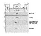
- FIG. 1is a simplified layer diagram illustrating a REO gate dielectric on a III-N device with a stress compensating REO template, in accordance with the present invention
- FIG. 2is a simplified layer diagram illustrating a specific example of a REO and Si stress compensating template
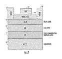
- FIG. 3is a simplified layer diagram illustrating a REO gate dielectric on a III-N device with a stress compensating AlN template, in accordance with the present invention.
- FIG. 1a simplified layer diagram is illustrated representing several steps in a process of growing a REO gate dielectric on a III-N device with a stress compensating REO template, in accordance with the present invention.
- silicon substrate 10is or may be a standard well known single crystal wafer or portion thereof generally known and used in the semiconductor industry.
- Single crystal substratesare not limited to any specific crystal orientation but could include (111) silicon, (110) silicon, (100) silicon or any other orientation or variation known and used in the art.
- the Si (100) and (111) substratescould also include various miscuts with nominal value between 0 and 10° in any direction.
- substrate 10is illustrated with a preferred (111) orientation because of the simplification of further operations.
- a stress compensating template 11 including rare earth oxide (REO)is epitaxially grown on silicon substrate 10 .
- Various rare earth oxideshave a crystal lattice spacing that can be matched to silicon with very little strain.
- Gd 2 O 3has a crystal lattice spacing (a) of 10.81 ⁇
- Er 2 O 3has a crystal lattice spacing (a) of 10.55 ⁇
- Nd 2 O 3has a crystal lattice spacing (a) of 11.08 ⁇
- siliconhas a double spacing ( 2 a ) of 10.86 ⁇ .
- the crystal lattice spacing of REO template 11can be varied by varying the composition of the constituents, which allows for strain engineering of the silicon wafers.
- REO template 11is a stress compensating template including one or more sub-layers (stepped or graded) of rare earth oxide defining, in conjunction with substrate 10 a “substrate structure”. Strain engineering mitigates the stresses formed during growth of III-N materials and devices on these substrate structures.
- REO template 11includes Gd 2 O 3 epitaxially grown on silicon substrate 10 with Er 2 O 3 epitaxially grown adjacent the opposite (upper) side.
- some REO materialshave a hexagonal crystal structure, rather than a cubic crystal structure, and REO template 11 can include some of these materials to gradually convert the template from cubic to hexagonal.
- the REO materialscan be grown in a graded fashion bridging the two compositions or split to have an abrupt change in the composition and/or constituents of template 11 .
- two constituentsare used in this example other and/or additional rare earth oxides can be included in template 11 .
- rare earth oxideis impervious to MBE process gasses, i.e. N 2 plasma, NH 3 and metallic Ga, which is the preferred growth process in this invention.
- MBE process gassesi.e. N 2 plasma, NH 3 and metallic Ga
- the rare earth oxideis also impervious to MOCVD process gasses (NH 3 , H 2 , TMGa, etc.). Reaction of silicon with process gasses usually results in etching of silicon (H 2 ), formation of nitrides (NH 3 ), or severe reaction and blistering (Ga precursor).
- REO template 11can be formed with a single continuous composition or it can be graded, in linear, stepwise or any similar schemes.
- GaN layer 12is epitaxially grown on REO template 11 preferably by an MBE process.
- GaN layer 12will be in a range of 50 nm to 100 nm thick, although thicker (as much as a micrometer) or thinner layers can be grown in some applications. Because there will still be some strain in GaN layer 12 , i.e. the crystal lattice junction with REO template 11 still produces some strain, a thinner layer 12 of GaN is preferred. Also, any of the structures outlined below for further reducing stress can be included if desired.
- AlN Inter-Layers in III-N Material Grown on REO/Silicon Substratea thin inter-layer of aluminum nitride (AlN) is epitaxially grown on the GaN layer to further reduce the strain.
- AlNaluminum nitride
- the AlN inter-layeris in a range of approximately 1 nm to approximately 10 nm thick but for certain applications thicker or thinner films can be grown.
- the AlN inter-layercan be grown using either a low or a high temperature process.
- a second layer of GaNis epitaxially grown on the AlN inter-layer.
- a second inter-layer of AlNis grown on the second GaN layer and this process is repeated n times or until the strain in the upper GaN or III-N layer has been reduced to an acceptable level.
- the strain formed during the growth of the GaNis controlled by insertion of the thin inter-layers of AlN, each of which allows the following layer of GaN to be under compressive stress due to the pseudomorphic growth at the interface. Repeating the process (i.e. the alternating growth of the GaN layers and the interlayers of AlN) n times can be used to further reduce or engineer strain in a final GaN or III-N layer.
- an AlN cap(not shown) can optionally be grown on the upper layer of the GaN/AlN interlayer structure to further reduce strain in an ultimate layer. Even with multiple Interlayers of AlN and GaN grown on REO stress compensating layer 11 there can be some strain when a III-N layer of material is grown on the upper surface.
- An AlN cap layercan provide a better match between the GaN/REO/silicon substrate structure and can substantially remove any strain that may remain between III material nitrides, especially any nitrides including aluminum.
- the AlN cap layerwill facilitate the growth of III-N materials and especially III-N materials including aluminum. Also, in some applications an AlN cap layer can reduce the number of times that the alternating growth of GaN layers and interlayers of AlN need to be repeated in order to reduce the strain in the final III-N layer.
- a single crystal layer 22 of cubic REO materialsuch as erbium oxide (or any other cubic rare earth oxides with an atomic number larger than gadolinium), is epitaxially grown on silicon substrate 21 .
- Silicon substrate 21is similar to substrate 10 described above.
- Single crystal layer 22 of cubic REO materialhas a crystal lattice spacing approximately ⁇ 3% (see explanation above) different than the double lattice spacing of silicon.
- a thin layer 24 of single crystal siliconis epitaxially grown on single crystal layer 22 and, because of the negative mismatch has a lattice spacing that is stretched to more closely match the spacing of single crystal layer 22 , i.e. layer 24 of the epitaxial silicon has a negative spacing different than the spacing of substrate 21 .
- a thin layer 26 of AlNis epitaxially grown on layer 24 of epitaxial silicon.
- AlN layer 26has a hexagonal crystal structure in which five lattice spacings are misfit from four standard silicon lattice spacings by ⁇ 1.2%. While this is sufficient to allow lattice coincident epitaxy, layer 24 of epitaxial silicon further reduces this misfit (i.e. below ⁇ 1.2%) so that better lattice matching is achieved with further reduction of dislocation density in AlN layer 26 .
- a layer 28 of GaNis epitaxially grown on AlN layer 26 which is illustrated as layer 12 in FIG. 1 .
- GaN layer 28has a hexagonal crystal structure which closely matches the hexagonal crystal structure of AlN.
- a thicker active layer of III-N material(layer 14 in FIG. 1 ) can then be epitaxially grown on layer 28 .
- any gallium containing layercannot be grown on silicon because gallium etches silicon and cannot touch silicon. Thus, the example described also protects the silicon from the gallium.
- a layer 14 of III-N semiconductor materialin this preferred example AlGaN, is epitaxially grown on layer 12 .
- Layer 14 of III-N semiconductor materialforms an active layer for semiconductor devices built on/in the surface thereof. Because III-N layer 14 is grown with very little stress due to the layers described above, it can be grown sufficiently thick to conveniently form electronic devices therein.
- a gate dielectric layer 16is epitaxially grown on the upper surface of III-N layer 14 .
- Gate dielectric layer 16is not crystal lattice matched to the III-N material of layer 14 because the lattice constant of the rare earth oxide is larger than the III-N.
- the REO materialis single crystal and is polymorphous which means the crystal structure is different than the crystal structure of bulk REO material.
- Bulk REO materialnormally has a cubic structure (the type of rare earth oxide used in the present case) while the crystal structure of the REO in gate dielectric layer 16 is monoclinic because it is grown on III-N layer 14 which has a hexagonal crystal structure.
- gate dielectric layer 16is epitaxially grown on the upper surface of III-N layer 14 , the various layers can be grown in situ, that is without removing the structure from the growth chamber, which substantially simplifies the method. Further, there is a large advantage in using the same materials for buffer layer 11 and gate dielectric layer 16 . This can be accomplished relatively easily when template 20 is used since it includes a single layer of REO material. Thus, the entire structure including template 11 and, layers 12 , 14 , and 16 can be grown on substrate 10 in one continuous operation. Layer 16 serves as a high k gate dielectric layer for a device formed thereon, such as a field effect transistor or the like. Also, because layer 16 is a single crystal material dangling bonds that could act as charge trap centers in any device are substantially avoided.
- a source and a draincan be formed in III-N active layer 14 by any well known method, such as implanting dopants.
- gate dielectric layer 16is grown and masked to define a channel in active layer 16 and the source/drain implants are automatically aligned. Source/drain contacts can then be formed in a typical metallization process and a gate stack 19 is formed on the upper surface of gate dielectric layer 16 . While this description only illustrates a single Field Effect Transistor (FET) for a complete understanding, it will be understood that anything from discrete devices to complete circuits can be formed using the same methods.
- FETField Effect Transistor
- FIG. 3an example is illustrated of a III-N device formed on another stress compensating template, in accordance with the present invention.
- components that are similar to components in FIG. 1are designated with a similar number having a prime (′) added to indicate the different example.
- the stress compensating template including cubic rare earth oxide (layer 11 )is replaced with an AlN stress compensating layer 11 ′.
- Layer 11 ′includes one or more layers including AlN and the layers can be stepped or graded in a well known process and may include other materials to reduce the misfit between AlN and Si.
- AlNis grown with a low temperature method especially prevalent when using MOCVD process, which results in the AlN lattice and the silicon lattice being misfit by approximately ⁇ 1.2% however for purposes of this disclosure the term “substantially crystal lattice matched” is defined to include a mismatch of ⁇ 1.2% or less.
- new and improved methods for the growth of III-N material and devices on a silicon substrateare disclosed.
- the new and improved methods for the III-N materialinclude the growth of a stress compensating template grown epitaxially on the silicon substrate.
- a high k rare earth gate dielectric layeris grown epitaxially on the substantially stress free III-N layer in what can be a continuous or in situ operation.
- the rare earth gate dielectric layerhas sufficient dielectric constant and a proper bandwidth offset for the formation of high performance electronic components, such as FETs and the like, in the III-N layer.
Landscapes
- Engineering & Computer Science (AREA)
- Microelectronics & Electronic Packaging (AREA)
- Computer Hardware Design (AREA)
- Physics & Mathematics (AREA)
- Condensed Matter Physics & Semiconductors (AREA)
- General Physics & Mathematics (AREA)
- Manufacturing & Machinery (AREA)
- Power Engineering (AREA)
- Chemical & Material Sciences (AREA)
- Crystallography & Structural Chemistry (AREA)
- Materials Engineering (AREA)
- Recrystallisation Techniques (AREA)
- Insulated Gate Type Field-Effect Transistor (AREA)
- Physical Deposition Of Substances That Are Components Of Semiconductor Devices (AREA)
- Thin Film Transistor (AREA)
- Crystals, And After-Treatments Of Crystals (AREA)
Abstract
Description
Claims (21)
Priority Applications (5)
| Application Number | Priority Date | Filing Date | Title |
|---|---|---|---|
| US13/774,962US8878188B2 (en) | 2013-02-22 | 2013-02-22 | REO gate dielectric for III-N device on Si substrate |
| PCT/US2014/010340WO2014130164A1 (en) | 2013-02-22 | 2014-01-06 | REO GATE DIELECTRIC FOR III-N DEVICE ON Si SUBSTRATE |
| JP2015559236AJP6304899B2 (en) | 2013-02-22 | 2014-01-06 | III-N semiconductor device grown on a silicon substrate with a rare earth oxide gate dielectric |
| EP14754064.5AEP2973658A4 (en) | 2013-02-22 | 2014-01-06 | RARE-EARTH OXIDE BASED GRID DIELECTRIC (REO) FOR A GROUP III (N-III) NITRIDE DEVICE ON A SILICON SUBSTRATE (SI) |
| US14/487,820US9431526B2 (en) | 2013-02-22 | 2014-09-16 | Heterostructure with carrier concentration enhanced by single crystal REO induced strains |
Applications Claiming Priority (1)
| Application Number | Priority Date | Filing Date | Title |
|---|---|---|---|
| US13/774,962US8878188B2 (en) | 2013-02-22 | 2013-02-22 | REO gate dielectric for III-N device on Si substrate |
Related Child Applications (1)
| Application Number | Title | Priority Date | Filing Date |
|---|---|---|---|
| US14/487,820Continuation-In-PartUS9431526B2 (en) | 2013-02-22 | 2014-09-16 | Heterostructure with carrier concentration enhanced by single crystal REO induced strains |
Publications (2)
| Publication Number | Publication Date |
|---|---|
| US20140239307A1 US20140239307A1 (en) | 2014-08-28 |
| US8878188B2true US8878188B2 (en) | 2014-11-04 |
Family
ID=51387239
Family Applications (1)
| Application Number | Title | Priority Date | Filing Date |
|---|---|---|---|
| US13/774,962Expired - Fee RelatedUS8878188B2 (en) | 2013-02-22 | 2013-02-22 | REO gate dielectric for III-N device on Si substrate |
Country Status (4)
| Country | Link |
|---|---|
| US (1) | US8878188B2 (en) |
| EP (1) | EP2973658A4 (en) |
| JP (1) | JP6304899B2 (en) |
| WO (1) | WO2014130164A1 (en) |
Cited By (5)
| Publication number | Priority date | Publication date | Assignee | Title |
|---|---|---|---|---|
| US20130248853A1 (en)* | 2012-03-20 | 2013-09-26 | Erdem Arkun | Nucleation of iii-n on reo templates |
| US20170141750A1 (en)* | 2015-11-13 | 2017-05-18 | IQE, plc | Layer structures for rf filters fabricated using rare earth oxides and epitaxial aluminum nitride |
| US10128350B2 (en) | 2016-09-22 | 2018-11-13 | Iqe Plc | Integrated epitaxial metal electrodes |
| US10418457B2 (en) | 2016-09-22 | 2019-09-17 | Iqe Plc | Metal electrode with tunable work functions |
| US11495670B2 (en) | 2016-09-22 | 2022-11-08 | Iqe Plc | Integrated epitaxial metal electrodes |
Families Citing this family (12)
| Publication number | Priority date | Publication date | Assignee | Title |
|---|---|---|---|---|
| US9159814B2 (en)* | 2013-03-26 | 2015-10-13 | Tsinghua University | Memory structure and method for forming same |
| FR3005202B1 (en)* | 2013-04-30 | 2016-10-14 | Commissariat Energie Atomique | METHOD FOR FORMING AN IMPLANTED AREA FOR A NORMALLY BLOCKED TYPE HETEROJUNCTION TRANSISTOR |
| US9130026B2 (en)* | 2013-09-03 | 2015-09-08 | Taiwan Semiconductor Manufacturing Co., Ltd. | Crystalline layer for passivation of III-N surface |
| US9425301B2 (en) | 2014-04-30 | 2016-08-23 | Taiwan Semiconductor Manufacturing Co., Ltd. | Sidewall passivation for HEMT devices |
| US9613803B2 (en) | 2015-04-30 | 2017-04-04 | International Business Machines Corporation | Low defect relaxed SiGe/strained Si structures on implant anneal buffer/strain relaxed buffer layers with epitaxial rare earth oxide interlayers and methods to fabricate same |
| US9960262B2 (en)* | 2016-02-25 | 2018-05-01 | Raytheon Company | Group III—nitride double-heterojunction field effect transistor |
| IT201700064147A1 (en)* | 2017-06-09 | 2018-12-09 | St Microelectronics Srl | HEMT TRANSISTOR NORMALLY OFF WITH SELECTIVE GENERATION OF 2DEG CHANNEL AND RELATIVE MANUFACTURING METHOD |
| WO2019159001A1 (en)* | 2018-02-15 | 2019-08-22 | Iqe Plc | Electronic device with 2-dimensional electron gas between polar-oriented rare-earth oxide layer grown over a semiconductor |
| CN111106171B (en)* | 2019-12-31 | 2024-03-19 | 晶能光电股份有限公司 | AlN barrier layer, alN/GaN HEMT epitaxial structure and growth method thereof |
| CN112993030A (en)* | 2021-02-04 | 2021-06-18 | 宁波海特创电控有限公司 | Method for improving reliability of groove grid GaN MIS FET device |
| CN118119729A (en)* | 2021-10-08 | 2024-05-31 | 东曹株式会社 | Laminated body and method for producing the same |
| GB2631915A (en)* | 2023-06-22 | 2025-01-22 | Iqe Plc | Semiconductor structures |
Citations (2)
| Publication number | Priority date | Publication date | Assignee | Title |
|---|---|---|---|---|
| US8633569B1 (en)* | 2013-01-16 | 2014-01-21 | Translucent, Inc. | AlN inter-layers in III-N material grown on REO/silicon substrate |
| US8680507B1 (en)* | 2013-01-16 | 2014-03-25 | Translucent, Inc. | A1N inter-layers in III-N material grown on DBR/silicon substrate |
Family Cites Families (13)
| Publication number | Priority date | Publication date | Assignee | Title |
|---|---|---|---|---|
| US6391748B1 (en)* | 2000-10-03 | 2002-05-21 | Texas Tech University | Method of epitaxial growth of high quality nitride layers on silicon substrates |
| US6645639B1 (en)* | 2000-10-13 | 2003-11-11 | Applied Thin Films, Inc. | Epitaxial oxide films via nitride conversion |
| US7432567B2 (en)* | 2005-12-28 | 2008-10-07 | International Business Machines Corporation | Metal gate CMOS with at least a single gate metal and dual gate dielectrics |
| JP5311765B2 (en)* | 2006-09-15 | 2013-10-09 | 住友化学株式会社 | Semiconductor epitaxial crystal substrate and manufacturing method thereof |
| US7675117B2 (en)* | 2006-11-14 | 2010-03-09 | Translucent, Inc. | Multi-gate field effect transistor |
| EP1975988B1 (en)* | 2007-03-28 | 2015-02-25 | Siltronic AG | Multilayered semiconductor wafer and process for its production |
| US8329541B2 (en)* | 2007-06-15 | 2012-12-11 | Taiwan Semiconductor Manufacturing Company, Ltd. | InP-based transistor fabrication |
| JP4784609B2 (en)* | 2008-01-21 | 2011-10-05 | Tdk株式会社 | Substrates for electronic devices |
| US8154038B2 (en)* | 2008-07-01 | 2012-04-10 | Taiwan Semiconductor Manufacturing Co., Ltd | Group-III nitride for reducing stress caused by metal nitride reflector |
| US8624260B2 (en)* | 2010-01-30 | 2014-01-07 | National Semiconductor Corporation | Enhancement-mode GaN MOSFET with low leakage current and improved reliability |
| US20120183767A1 (en)* | 2010-02-19 | 2012-07-19 | Rytis Dargis | Hexagonal reo template buffer for iii-n layers on silicon |
| JP2011198837A (en)* | 2010-03-17 | 2011-10-06 | Renesas Electronics Corp | Semiconductor device and method of manufacturing the same |
| KR101813177B1 (en)* | 2011-05-06 | 2017-12-29 | 삼성전자주식회사 | High electron mobility transistor and method of manufacturing the same |
- 2013
- 2013-02-22USUS13/774,962patent/US8878188B2/ennot_activeExpired - Fee Related
- 2014
- 2014-01-06EPEP14754064.5Apatent/EP2973658A4/ennot_activeWithdrawn
- 2014-01-06WOPCT/US2014/010340patent/WO2014130164A1/enactiveApplication Filing
- 2014-01-06JPJP2015559236Apatent/JP6304899B2/ennot_activeExpired - Fee Related
Patent Citations (2)
| Publication number | Priority date | Publication date | Assignee | Title |
|---|---|---|---|---|
| US8633569B1 (en)* | 2013-01-16 | 2014-01-21 | Translucent, Inc. | AlN inter-layers in III-N material grown on REO/silicon substrate |
| US8680507B1 (en)* | 2013-01-16 | 2014-03-25 | Translucent, Inc. | A1N inter-layers in III-N material grown on DBR/silicon substrate |
Cited By (9)
| Publication number | Priority date | Publication date | Assignee | Title |
|---|---|---|---|---|
| US20130248853A1 (en)* | 2012-03-20 | 2013-09-26 | Erdem Arkun | Nucleation of iii-n on reo templates |
| US9496132B2 (en)* | 2012-03-20 | 2016-11-15 | Translucent, Inc. | Nucleation of III-N on REO templates |
| US20170141750A1 (en)* | 2015-11-13 | 2017-05-18 | IQE, plc | Layer structures for rf filters fabricated using rare earth oxides and epitaxial aluminum nitride |
| US10075143B2 (en)* | 2015-11-13 | 2018-09-11 | IQE, plc | Layer structures for RF filters fabricated using rare earth oxides and epitaxial aluminum nitride |
| US10566944B2 (en) | 2015-11-13 | 2020-02-18 | Iqe Plc | Layer structures for RF filters fabricated using rare earth oxides and epitaxial aluminum nitride |
| US10128350B2 (en) | 2016-09-22 | 2018-11-13 | Iqe Plc | Integrated epitaxial metal electrodes |
| US10418457B2 (en) | 2016-09-22 | 2019-09-17 | Iqe Plc | Metal electrode with tunable work functions |
| US10825912B2 (en) | 2016-09-22 | 2020-11-03 | Iqe Plc | Integrated epitaxial metal electrodes |
| US11495670B2 (en) | 2016-09-22 | 2022-11-08 | Iqe Plc | Integrated epitaxial metal electrodes |
Also Published As
| Publication number | Publication date |
|---|---|
| JP2016515299A (en) | 2016-05-26 |
| US20140239307A1 (en) | 2014-08-28 |
| WO2014130164A1 (en) | 2014-08-28 |
| EP2973658A1 (en) | 2016-01-20 |
| EP2973658A4 (en) | 2016-11-30 |
| JP6304899B2 (en) | 2018-04-04 |
Similar Documents
| Publication | Publication Date | Title |
|---|---|---|
| US8878188B2 (en) | REO gate dielectric for III-N device on Si substrate | |
| JP4530171B2 (en) | Semiconductor device | |
| US9431526B2 (en) | Heterostructure with carrier concentration enhanced by single crystal REO induced strains | |
| KR101854021B1 (en) | P-doping of group-iii-nitride buffer layer structure on a heterosubstrate | |
| US7709859B2 (en) | Cap layers including aluminum nitride for nitride-based transistors | |
| US8633569B1 (en) | AlN inter-layers in III-N material grown on REO/silicon substrate | |
| EP3501033B1 (en) | Semiconductor material growth of a high resistivity nitride buffer layer using ion implantation | |
| US8823055B2 (en) | REO/ALO/A1N template for III-N material growth on silicon | |
| US20110108885A1 (en) | Semiconductor device and method of manufacturing a semiconductor device | |
| JP2003059948A (en) | Semiconductor device and production method therefor | |
| US10340345B2 (en) | Nitride semiconductor epitaxial wafer and field effect nitride transistor | |
| CN112701160A (en) | Gallium nitride-based high-electron-mobility transistor epitaxial wafer and preparation method thereof | |
| US8872308B2 (en) | AlN cap grown on GaN/REO/silicon substrate structure | |
| US8748900B1 (en) | Re-silicide gate electrode for III-N device on Si substrate | |
| CN111406306B (en) | Semiconductor device manufacturing method, semiconductor device | |
| JP7068676B2 (en) | Non-etched gas-cooled epitaxial stack for group IIIA-N devices | |
| US8994032B2 (en) | III-N material grown on ErAIN buffer on Si substrate | |
| US10629475B2 (en) | Semiconductor device with two-part insulation structure within non-active region | |
| WO2019118473A1 (en) | Methods for transistor epitaxial stack fabrication | |
| US8823025B1 (en) | III-N material grown on AIO/AIN buffer on Si substrate | |
| CN100501951C (en) | Field effect transistor, semiconductor device, method of manufacturing the same, and method of growing semiconductor crystal | |
| US11646357B2 (en) | Method for preparing a p-type semiconductor structure, enhancement mode device and method for manufacturing the same | |
| TW201909276A (en) | Semiconductor devices and methods for forming the same |
Legal Events
| Date | Code | Title | Description |
|---|---|---|---|
| AS | Assignment | Owner name:TRANSLUCENT, INC., CALIFORNIA Free format text:ASSIGNMENT OF ASSIGNORS INTEREST;ASSIGNORS:DARGIS, RYTIS;SMITH, ROBIN;CLARK, ANDREW;AND OTHERS;SIGNING DATES FROM 20140916 TO 20140919;REEL/FRAME:033789/0516 | |
| STCF | Information on status: patent grant | Free format text:PATENTED CASE | |
| MAFP | Maintenance fee payment | Free format text:PAYMENT OF MAINTENANCE FEE, 4TH YR, SMALL ENTITY (ORIGINAL EVENT CODE: M2551) Year of fee payment:4 | |
| AS | Assignment | Owner name:IQE PLC, UNITED KINGDOM Free format text:ASSIGNMENT OF ASSIGNORS INTEREST;ASSIGNOR:TRANSLUCENT INC.;REEL/FRAME:046329/0511 Effective date:20180413 | |
| FEPP | Fee payment procedure | Free format text:ENTITY STATUS SET TO UNDISCOUNTED (ORIGINAL EVENT CODE: BIG.); ENTITY STATUS OF PATENT OWNER: LARGE ENTITY Free format text:PETITION RELATED TO MAINTENANCE FEES GRANTED (ORIGINAL EVENT CODE: PTGR); ENTITY STATUS OF PATENT OWNER: LARGE ENTITY | |
| MAFP | Maintenance fee payment | Free format text:PAYMENT OF MAINTENANCE FEE UNDER 1.28(C) (ORIGINAL EVENT CODE: M1559); ENTITY STATUS OF PATENT OWNER: LARGE ENTITY | |
| FEPP | Fee payment procedure | Free format text:MAINTENANCE FEE REMINDER MAILED (ORIGINAL EVENT CODE: REM.); ENTITY STATUS OF PATENT OWNER: LARGE ENTITY | |
| LAPS | Lapse for failure to pay maintenance fees | Free format text:PATENT EXPIRED FOR FAILURE TO PAY MAINTENANCE FEES (ORIGINAL EVENT CODE: EXP.); ENTITY STATUS OF PATENT OWNER: LARGE ENTITY | |
| STCH | Information on status: patent discontinuation | Free format text:PATENT EXPIRED DUE TO NONPAYMENT OF MAINTENANCE FEES UNDER 37 CFR 1.362 | |
| FP | Lapsed due to failure to pay maintenance fee | Effective date:20221104 |