US8874814B2 - Switch-state information aggregation - Google Patents
Switch-state information aggregationDownload PDFInfo
- Publication number
- US8874814B2 US8874814B2US13/157,519US201113157519AUS8874814B2US 8874814 B2US8874814 B2US 8874814B2US 201113157519 AUS201113157519 AUS 201113157519AUS 8874814 B2US8874814 B2US 8874814B2
- Authority
- US
- United States
- Prior art keywords
- switch
- input
- switches
- state
- coupled
- Prior art date
- Legal status (The legal status is an assumption and is not a legal conclusion. Google has not performed a legal analysis and makes no representation as to the accuracy of the status listed.)
- Active, expires
Links
Images


Classifications
- H—ELECTRICITY
- H03—ELECTRONIC CIRCUITRY
- H03M—CODING; DECODING; CODE CONVERSION IN GENERAL
- H03M11/00—Coding in connection with keyboards or like devices, i.e. coding of the position of operated keys
- H03M11/22—Static coding
- H03M11/24—Static coding using analogue means, e.g. by coding the states of multiple switches into a single multi-level analogue signal or by indicating the type of a device using the voltage level at a specific tap of a resistive divider
Definitions
- I/Oinput/output
- the microprocessormonitors the state of the switches by polling each of the switches to check the state of the switches.
- an I/O expander or a programmable logic devicecan be used to share the microprocessor I/O interfaces among the monitored switches.
- the microprocessortypically must implement a protocol for interacting with the I/O expander or PLD and for addressing the individual switches.
- the amount of time required for the microprocessor to poll all of the switches through an I/O expander or PLDmay be undesirable or unacceptable for some applications.
- the I/O interface that is used to monitor the state of the switchis typically not able to be used for other purposes. For example, where one state of each switch is used to determine when to read from or write to a memory device associated with that switch, another I/O interface or line would typically be needed for the microprocessor to read from or write to the memory device.
- One exemplary embodimentis directed to a system that comprises a plurality of switches, each having a respective logical binary state.
- the systemfurther comprises a programmable processor to monitor the state of the plurality of switches.
- the systemfurther comprises a digital-to-analog converter that converts a binary code presented on inputs of the digital-to-analog converter into an analog signal proportional to the binary code.
- the systemis configured so that each of at least some of the inputs of the digital-to-analog converter is coupled to a respective one of the plurality of switches such that each such input is indicative of the state of the respective switch coupled thereto.
- the state of the plurality of switchesis communicated to the programmable processor at least in part using the analog signal output by the digital-to-analog converter.
- An analog-to-digital conversionis performed on the analog signal output by the digital-to-analog converter to produce a digital representation of the state of the plurality of switches.
- Another exemplary embodimentis directed to a system that comprises a plurality of switches, each having a respective logical binary state.
- the systemfurther comprises a programmable processor to monitor the state of the plurality of switches, the programmable processor comprising a plurality of input/output lines.
- Each of the plurality of switchesis coupled to a respective input/output line.
- the systemFor each of the plurality of switches, the system is configured to develop a first logic state on the input/output line associated with that switch when that switch is in a first switch state.
- the systemis configured to develop a second logic state on the input/output line associated with that switch when that switch is in a second switch state.
- the systemis further configured to enable data other than the first and second logic states to be communicated over the input/output lines.
- FIG. 1is a block diagram of one embodiment of a system that is configured to monitor the state of a plurality of switches.
- FIG. 2is a graph showing the corresponding output voltage for each of the 256 possible binary codes that can be presented on the inputs of the DAC shown in FIG. 1 .
- FIG. 3is a flow diagram of one embodiment of a method of monitoring the state of a plurality of switches.
- FIG. 4is a block diagram of one embodiment of a patch panel that uses the switch-state aggregation techniques described above.
- FIG. 5is a block diagram of another embodiment of a system that is configured to monitor the state of a plurality of switches.
- FIGS. 6 and 7are block diagrams of exemplary embodiments of a circuits that can be used to couple one of the switches to the processor in the system of FIG. 5 .
- FIG. 8is a flow diagram of one embodiment of a method of monitoring the state of a plurality of switches.
- FIG. 9is a block diagram of one embodiment of a patch panel that uses the switch-state aggregation techniques described above in connection with FIGS. 5-8 .
- FIG. 10is a block diagram of another embodiment of a system that is configured to monitor the state of a plurality of switches.
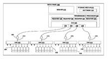
- FIG. 1is a block diagram of one embodiment of a system 100 that is configured to monitor the state of a plurality of switches 102 .
- a “switch”refers to any component or device that is actuated (or otherwise switched) between two logical states (for example, a logical “open” state and a logical “closed” state, a logical “on” state and a logical “off” state, or a logical “0” state and a logical “1” state). These states of the switch are also referred to here as “switch states”.
- each of the switches 102has a respective logical binary state that is one of the two logical states.
- switchesinclude, without limitation, electromechanical switches such as a single-pole, single-throw (SPST) switch or a shorting contact on an electronic component or sub-assembly that completes a circuit upon insertion into an assembly, and fully electronic switches such as an operational amplifier output, a metal-oxide-semiconductor field-effect transistor (MOSFET), or a logical gate.
- SPSTsingle-pole, single-throw
- MOSFETmetal-oxide-semiconductor field-effect transistor
- a programmable processor 104executes software 106 for, among other things, monitoring the state of the plurality of switches 102 .
- the software 106comprises program instructions that are stored (or otherwise embodied) on or in an appropriate non-transitory storage medium or media 108 (such as flash or other non-volatile memory, magnetic disc drives, and/or optical disc drives) from which at least a portion of the program instructions are read by the programmable processor 104 for execution thereby.
- the storage medium 108 on or in which the program instructions are embodiedis also referred to here as a “program product”. Although the storage medium 108 is shown in FIG.
- the system 100also includes memory 110 for storing the program instructions (and any related data) during execution by the programmable processor 104 .
- Memory 110comprises, in one implementation, any suitable form of random access memory (RAM) now known or later developed, such as dynamic random access memory (DRAM). In other embodiments, other types of memory are used.
- RAMrandom access memory
- DRAMdynamic random access memory
- the systemfurther comprises a digital-to-analog converter (DAC) 112 .
- the DAC 112converts a binary code presented on its inputs 114 into an analog signal that is proportional to the binary code. That is, the inputs 114 of the DAC 112 correspond to the binary digits of the binary code that is presented to the DAC 112 .
- the analog signalis output on the voltage output (VOUT) 116 of the DAC 112 .
- At least some of the inputs 114 of the digital-to-analog converter 112are coupled to a respective one of the plurality of switches 102 such that each such input 114 is indicative of the state of the respective switch 102 coupled to that input 114 . In this way, the binary code that is presented on the inputs 114 of the DAC 112 is indicative of the state of the switches 102 .
- an 8-bit, voltage-mode, parallel DACis used.
- the DAC 112has eight inputs 114 , which are referred to here individually as D 0 , D 1 , D 2 , D 3 , D 4 , D 5 , D 6 , and D 7 .
- six switches 102are shown. Inputs D 0 and D 1 are coupled to ground while inputs D 1 , D 2 , D 3 , D 4 , D 5 , D 6 , and D 7 are coupled to a respective one of the six switches 102 .
- the switches 102are configured so that, when the switch 102 is in a first state, a first digital voltage level (VREF) corresponding to a digital “1” is presented on the respective input 114 of the DAC 112 and, when the switch 102 is in a second state, a second digital voltage level corresponding to a digital “0” is presented on the respective input 114 of the switch 102 .
- VREFfirst digital voltage level
- Inputs D 0 and D 1are coupled to ground in order to improve the noise sensitivity of the system 100 because the smaller voltage weights given to inputs D 0 and D 1 are not used (and need not be detected by the ADC 124 described below). However, in other embodiments, all of the inputs of the DAC are coupled to switches.
- the DAC 112comprises a R2R resistor ladder 118 , the output 116 of which is connected to the input of a unity gain buffer amplifier 120 .
- the R2R resistor ladder 118is provided with two reference voltage supply levels (in this embodiment, VREF (which is associated with a logical “1”) and ground (which is associated with a logical “0”), which are the “rails” of the R2R resistor ladder 118 .
- the R2R resistor ladder 118comprises a respective resistor stage 122 for each of the binary inputs D 0 , D 1 , D 2 , D 3 , D 4 , D 5 , D 6 , and D 7 , which provides an appropriate weighting for each binary input's contribution to the output voltage VOUT.
- Table 1shows the corresponding voltage weight associated with each binary digit of the binary code presented on the inputs 114 of the DAC 112 , where input D 0 is the least significant bit (LSB), input D 7 is the most significant bit (MSB), VREF is equal to 5 Volts, and the resistors in the RSR resistor ladder 118 have the values shown in FIG. 1 .
- FIG. 2is a graph showing the corresponding output voltage VOUT for each of the 256 possible binary codes that can be presented on the inputs 114 of the DAC 112 .
- the switches 102 associated with inputs D 7 , D 6 and D 2are in the state that is associated with the binary value “1” (for example, if those switches 102 are closed) and the switches 102 associated with inputs D 5 , D 4 , and D 3 are in the state that is associated with the binary value “0” (for example, if those switches 102 are open), and the inputs D 1 and D 0 are connected to ground, then the binary code “11000100” is presented on the inputs 114 of the DAC 112 .
- the DAC 112In response to that binary code being presented on the inputs 114 of the DAC 112 , the DAC 112 outputs an analog signal having an output voltage of 2.555 Volts, which is 1 ⁇ 1.67 Volts+1 ⁇ 833 millivolts+0 ⁇ 416 millivolts+0 ⁇ 208 millivolts+0 ⁇ 104 millivolts+1 ⁇ 52 millivolts+0 ⁇ 26 millivolts+0 ⁇ 13 millivolts.
- the unity gain buffer amplifier 120 shown in FIG. 1can be implemented, for example, by connecting the output VOUT of the DAC 112 to the non-inverting input of an operational amplifier whose output is tied back to the inverting input of the operational amplifier.
- the analog output of the unity gain buffer amplifier 120is input to an analog-to-digital converter (ADC) 124 , which converts the analog output back to a binary code proportional to the analog signal output by the DAC 112 .
- the binary code that is output by the ADC 124is a digital representation of the state of the switches 102 .
- the programmable processor 104includes the ADC 124 (though in other embodiment an external ADC can be used).
- the programmable processor 104periodically updates the contents of a register 126 with the binary code that is output by the ADC 124 .
- Software 106 executing on the programmable processor 104monitors the state of the plurality of switches 102 by monitoring the state of the register 126 . As a result, the software 106 need not scan the individual switches 102 in order to monitor the state of the switches 102 .
- FIG. 3is a flow diagram of one embodiment of a method 300 of monitoring the state of a plurality of switches.
- the embodiment of method 300 shown in FIG. 3is described here as being implemented in the system 100 of FIG. 1 in order to aggregate state information for the plurality of switches 102 , though other embodiments can be implemented in other ways.
- Method 300comprises converting a binary code presented on the inputs 114 of the DAC 112 to an analog signal proportional to the binary code (block 302 ).
- the binary code that is presented on the inputs of the DAC 112is made up of eight binary values, where the binary values presented on the inputs D 2 , D 3 , D 4 , D 5 , D 6 , and D 7 are indicative of the state of a respective one of the plurality of switches 102 .
- the inputs D 0 and D 1are connected to ground (that is, the binary value “0”) in order to improve noise sensitivity.
- the switches 102 associated with inputs D 7 , D 6 and D 2are in the state that is associated with the binary value “1” (for example, if those switches 102 are closed)
- the switches 102 associated with inputs D 5 , D 4 , and D 3are in the state that is associated with the binary value “0” (for example, if those switches 102 are open)
- the inputs D 1 and D 0are connected to ground
- the binary code “11000100”is presented on the inputs 114 of the DAC 112 .
- the DAC 112In response to that binary code being presented on the inputs of the DAC 112 , the DAC 112 would output an analog signal having an output voltage of 2.555 Volts, which is 1 ⁇ 1.67 Volts+1 ⁇ 833 millivolts+0 ⁇ 416 millivolts+0 ⁇ 208 millivolts+0 ⁇ 104 millivolts+1 ⁇ 52 millivolts+0 ⁇ 26 millivolts+0 ⁇ 13 millivolts.
- Method 300further comprises communicating state information for the plurality of switches 102 using the analog signal (block 304 ).
- the output of the DAC 112is the buffered and amplified by the unity gain buffer amplifier 120 .
- the resulting amplified analog signal(and the aggregated state information for the plurality of switches 102 that it represents) is communicated to the ADC 124 included in the programmable processor 104 .
- Method 300further comprises converting the analog signal to a binary code proportional to the analog output using the ADC 124 (block 306 ).
- the binary code that is output by the ADC 124is a digital representation of the state of the switches 102 .
- the programmable processor 104includes the ADC 124 , though in other embodiment an external ADC can be used.
- the programmable processor 104periodically updates the contents of the register 126 with the binary code that is output by the ADC 124 .
- the ADC 124upon receiving an analog signal output from that DAC 112 having a voltage of 2.555 Volts, would reconstruct the binary code “110000100” from that analog output and place it into the register 126 .
- Method 300further comprises monitoring the output of the ADC 124 in order to monitor the state of the plurality of switches 102 (block 308 ).
- software 106 executing on the programmable processor 104monitors the state of the plurality of switches 102 by monitoring the contents of the register 126 . For example, when a bit in the register 126 changes, that indicates that the state of the corresponding switch 102 has changed.
- the analog signal output by the unity gain buffer amplifier 120need be communicated to the ADC 124 in the programmable processor 104 in order to provide it with state information for all of the switches 102 (as opposed to having to provide a separate signal for each of the plurality of switches 102 and/or using an I/O expander or PLD). Also, by monitoring the register 126 , the software 106 executing on the programmable processor 104 can monitor the state of the switches 102 without having to scan or poll the individual switches 102 .
- an 8-bit, parallel DAC having a voltage (amplitude) outputis used.
- other types of DACsare used.
- a digital-to-analog converterhaving a different resolution, a serial input interface, and/or an analog output with a different attribute that is proportional to the binary code presented on the inputs (for example, a voltage attribute other than amplitude (such as a pulse width) that is proportional to the binary code presented on the inputs or a current attribute that is proportional to the binary code presented on the inputs).
- the ADC 124is a part of the programmable processor 104 .
- the ADC 124is separate from the programmable processor, in which case the output of the ADC 124 is provided on an appropriate input or inputs to the programmable processor.
- less than all of the inputs 114 of the DAC 112are coupled to switches 102 in order to improve noise sensitivity.
- all of the inputs of the DACare coupled to switches.
- a single DAC 112 and single ADC 124are used in the embodiment described in connection with FIGS. 1-3 , in other embodiments multiple digital-to-analog converters and/or multiple analog-to-digital converters are used.
- switch state aggregation techniques described abovecan be used in a variety of applications to aggregate and monitor switch-state information.
- FIG. 4is a block diagram of one embodiment of a patch panel 400 that uses the switch-state aggregation techniques described above.
- the patch panel 400is typically mounted (along with other patch panels) in a rack located, for example, in a telecommunications closet, server room, or data center.
- the patch panel 400comprises a plurality of ports 402 .
- Each port 402is configured to attach a cable (or other segment of communication media) to the port 402 in a semi-permanent manner.
- a “semi-permanent” attachmentis one that is designed to be changed relatively infrequently, if ever. This is also referred to sometimes as a “one-time” connection.
- Such a cableis also referred to here as a “fixed” cable.
- Such connectionscan be made using punch-down blocks (in the case of copper communication media) and fiber adapters, fiber splice points, and fiber termination points (in the case of fiber communication media).
- Each port 402is also configured to attach a second cable to the port 402 using a connector.
- a cableis also referred to here as a “connectorized” cable or “patch cord”.
- the port 402includes a suitable connector, adapter, or jack that mates with the corresponding connector on the end of the patch cord.
- the connectoris used to facilitate the easy and repeated attachment and unattachment of the connectorized media segment to the port 402 .
- Examples of connectorized cablesinclude CAT-5, 6, and 7 twisted-pair cables having modular connectors or plugs attached to both ends (in which case, the patch cords 402 include compatible modular jacks) or fiber cables having SC, LC, FC, LX.5, MTP, or MPO connectors (in which case, the patch cords 402 include compatible SC, LC, FC, LX.5, MTP, or MPO connectors or adapters).
- the techniques described herecan be used with other types of connectors including, for example, BNC connectors, F connectors, DSX jacks and plugs, bantam jacks and plugs, and MPO and MTP multi-fiber connectors and adapters.
- Each port 402communicatively couples the respective fixed cable to the respective connector of any patch cord inserted into that port 402 .
- each port 402is designed for use with a fixed cable and a patch cord that comprise the same type of physical communication media, in which case each port 402 communicatively couples the fixed cable to the patch cord at the physical layer level without any media conversion.
- each port 402communicatively couples the fixed cable to the patch cord in other ways (for example, using a media converter if the fixed cable and the patch cord comprise different types of physical communication media).
- Each port 402has associated with it a respective switch 404 .
- Each switch 404is configured to be in a first state when a patch cord connector attached to a patch cord is not inserted in that port 402 and to be in a second state when a patch cord connector is inserted in that port 402 .
- an electromechanical switchis used where, when no patch cord connector is inserted into the corresponding port 402 , the switch is in a first (open) state and, when a patch cord connector is inserted into the corresponding port 402 , the switch is in a second (closed) state.
- an infrared non-contact switchin which an infrared emitting diode produces an infrared beam that is detected by a corresponding infrared detector.
- the infrared detectorwhen no patch cord connector is inserted into the corresponding port 402 , the infrared detector is able to detect the infrared beam and the switch is considered to be in a first state.
- the infrared detectorWhen a patch cord connector is inserted into the corresponding port 402 , the infrared detector is not able to detect the infrared beam because the connector blocks the infrared beam and prevents it from reaching the infrared detector, in which case the switch is considered to be in a second state.
- other types of switchesare used. Examples of suitable switches 404 are described in the '208 application and the '961 application.
- a programmable processor 406is mounted to the patch panel 400 .
- the programmable processor 406executes software 408 for, among other things, monitoring the state of the switches 404 for the patch panel 400 .
- the software 408comprises program instructions that are stored (or otherwise embodied) on or in an appropriate non-transitory storage medium or media 410 (such as flash or other non-volatile memory, magnetic disc drives, and/or optical disc drives) from which at least a portion of the program instructions are read by the programmable processor 406 for execution thereby.
- the storage medium 410 on or in which the program instructions are embodiedis also referred to here as a “program product”. Although the storage medium 410 is shown in FIG.
- the patch panel 400also includes memory 412 for storing the program instructions (and any related data) during execution by the programmable processor 406 .
- Memory 412comprises, in one implementation, any suitable form of random access memory (RAM) now known or later developed, such as dynamic random access memory (DRAM). In other embodiments, other types of memory are used.
- RAMrandom access memory
- DRAMdynamic random access memory
- the patch panel 400includes four digital-to-analog converters (DAC) 414 .
- Each DAC 414functions in the same manner as DAC 112 described above in connection FIG. 1 .
- Each DAC 414converts a binary code presented on its inputs 416 into an analog signal that is proportional to the binary code. That is, the inputs 416 of each DAC 414 correspond to the binary digits of the binary code that is presented to that DAC 414 .
- the analog signalis presented on the output 418 of that DAC 414 .
- the patch panel 400includes 24 ports 402 and a 24 switches 404 . In this embodiment, six of the inputs of each DAC 414 (the inputs corresponding the six most significant binary digits) are coupled to six of the switches 404 .
- each DAC 414is connected to the input of a separate unity gain buffer amplifier 420 .
- the programmable processor 406includes an analog-to-digital converter 422 that has a separate channel 424 for each of the eight DACs 414 .
- the ADC 422 in the programmable processor 410has at least four ADC channels 424 .
- the ADC 422for each of the four ADC channels 424 , converts the analog output received on that channel 424 back to a binary code that is proportional to the received analog output.
- the binary code that is output by the ADC 422 for each ADC channel 424is a digital representation of the state of the switches 404 that are connected to the DAC 414 that produced the analog output signal.
- the programmable processor 406includes the ADC 422 , though in other embodiments an external ADC can be used.
- the programmable processor 406includes a separate register 426 for each ADC channel 424 .
- the ADC 422periodically updates the contents of the associated register 430 with the binary code output by the ADC 422 for that ADC channel 424 .
- a patch cord being inserted into a port 402causes the corresponding switch 404 to enter a state that is associated with a logical “1” and a patch cord being removed from a port 402 causes the corresponding switch 404 to enter a state that is associated with a logical “0”.
- a binary code “11000100”would be presented on the inputs 416 of that DAC 414 .
- DAC 414would output a voltage of 2.555 Volts, which is 1 ⁇ 1.67 Volts+1 ⁇ 833 millivolts+0 ⁇ 416 millivolts+0 ⁇ 208 millivolts+0 ⁇ 104 millivolts+1 ⁇ 52 millivolts+0 ⁇ 26 millivolts+0 ⁇ 13 millivolts.
- the ADC 422upon receiving the analog signal output having that voltage from the DAC 414 would reconstruct the binary code “110000100” from the analog output and place it into the contents of the corresponding register 426 .
- the software 408 executing on the programmable processor 406monitors the state of the plurality of switches 404 by monitoring the contents of the registers 426 . As a result, the software 408 need not scan the individual switches 404 in order to monitor state of the switches 404 .
- the programmable processor 406can be implemented using an 8-bit central processing unit (CPU) having an ADC that takes about 20 microseconds to produce a digital output for a given analog channel. This is considerably faster than the time that would typically be required to scan each of the switches 404 using a conventional I/O expander/addressing scheme.
- each of the port 402has a respective media reading interface 428 via which the programmable processor 406 is able to read any identifier and attribute information stored in or on any patch cord that is inserted into that port 402 .
- the programmable processor 406is communicatively coupled to each of the media reading interfaces 428 using a suitable bus or other interconnect (not shown). Additional details regarding such an embodiment can be found in the '624 application.
- the insertioncauses the switch 404 associated with that port 402 to be actuated (or otherwise switched) and changed from the state associated with no patch cord being inserted in the port 402 (for example, a logical “0”) to the state associated with a patch cord being inserted in the port 402 (for example, a logical “1”).
- the programmable processor 406monitors the registers 426 to determine when a patch cord has been inserted into a port 402 and when it detects that the state of given switch 404 has changed from the state associated with no patch cord being inserted in the port 402 to the state associated with a patch cord being inserted in the port 402 , the programmable processor 406 reads the identifier and attribute information stored in or on the patch cord that was inserted into that port 402 using the appropriate media reading interface 428 .
- FIG. 5is a block diagram of another embodiment of a system 500 that is configured to monitor the state of a plurality of switches 502 .
- a programmable processor 504executes software 506 for, among other things, monitoring the state of the plurality of switches 502 .
- the software 506comprises program instructions that are stored (or otherwise embodied) on or in an appropriate non-transitory storage medium or media 508 (such as flash or other non-volatile memory, magnetic disc drives, and/or optical disc drives) from which at least a portion of the program instructions are read by the programmable processor 504 for execution thereby.
- the storage medium 508 on or in which the program instructions are embodiedis also referred to here as a “program product”.
- the storage medium 508is shown in FIG. 5 as being included in, and local to, the system 500 , it is to be understood that removable media and/or remote storage media (for example, storage media that is accessible over a network) can also be used.
- the system 500also includes memory 510 for storing the program instructions (and any related data) during execution by the programmable processor 504 .
- Memory 510comprises, in one implementation, any suitable form of random access memory (RAM) now known or later developed, such as dynamic random access memory (DRAM). In other embodiments, other types of memory are used.
- RAMrandom access memory
- DRAMdynamic random access memory
- the processor 504comprises a plurality of input/output (I/O) lines 524 .
- the I/O lines 524comprise a plurality of serial communication I/O lines that can be individually read by the processor 504 .
- Each of the switches 502is coupled to a respective I/O line 524 .
- the I/O lines 524are a part of a register set that can be read from or written to simultaneously.
- the system 500includes a separate circuit 528 for each switch 502 that is configured to develop a first logic state on the input/output line 524 associated with that switch 502 when that switch 502 is in a first switch state (for example, when the switch 502 is in a closed state) and to develop a second logic state on the input/output line 524 associated with that switch 502 when that switch 502 is in a second switch state (for example, when the switch 502 is in an open state).
- the software 506 executing on the processor 504monitors the state of the plurality of switches 502 by reading the I/O lines 524 as a register. In this way, the software 506 need not scan the individual switches 502 (nor the individual I/O lines 524 ) in order to monitor the state of the switches 502 .
- each switch 502is configured to enable data other than the state of the switch 502 to be communicated over the input/output lines 524 .
- the same input/output lines 524can be used both to detect the status of the switch 502 and to communicate other data, thereby reducing the number of overall input/output lines needed to carry out both functions.
- each input/output line 524is used to read from and/or write to a memory device (such as a UNI/O electrically erasable programmable read only memory (EEPROM) device).
- EEPROMelectrically erasable programmable read only memory
- FIG. 6is a block diagram of an exemplary embodiment of a circuit 600 that can be used to couple one of the switches 502 to the processor 504 in the system 500 of FIG. 5 .
- the exemplary circuit 600 shown in FIG. 6is designed for use where each switch 502 is implemented using a normally closed switch.
- a pull-up resistor 610is coupled to a supply voltage 612 and to a first terminal 614 of the normally closed switch 502 .
- a second terminal 616 of the normally closed switch 502is coupled to ground.
- the input/output line 524 for that switch 502is also coupled to the first terminal 614 of the normally closed switch 502 .
- the first terminal 614is coupled to ground, which causes an idle logic low state to be developed on the input/output line 524 .
- the first terminal 614is coupled to the supply voltage 612 via the pull-up resistor 610 , which causes an idle logic high state to be developed on the input/output line 524 .
- the circuit 600is also configured to enable data other than the state of the switch 502 to be communicated over the input/output line 524 when the switch 502 is opened.
- a memory devicesuch as a UNI/O EEPROM
- the memory device coupled to the input/output line 524can still pull the input/output line 524 to ground in order to output a logic low.
- the pull-up resistor 610is implemented using a 20 k Ohm resistor.
- FIG. 7is a block diagram of an exemplary embodiment of a circuit 700 that can be used to couple one of the switches 502 to the processor 504 in the system 500 of FIG. 5 .
- the exemplary circuit 700 shown in FIG. 7is designed for use where each switch 502 is implemented using a normally open switch.
- a pull-up resistor 710is coupled to a supply voltage 712 and to a first terminal 714 of the normally open switch 502 .
- a second terminal 716 of the normally open switch 502is coupled to ground via a weak pull-down resistor 718 .
- the input/output line 524 for that switch 502is also coupled to the second terminal 716 of the normally open switch 502 .
- the second terminal 716is coupled to ground via the weak pull-down resistor 718 , which causes an idle logic low state to be developed on the input/output line 524 .
- the first terminal 714is coupled to the supply voltage 712 via the pull-up resistor 710 , which causes an idle logic high state to be developed on the input/output line 524 .
- the circuit 700is also configured to enable data other than the state of the switch 502 to be communicated over the input/output line 524 when the switch 502 is closed.
- a memory devicesuch as a UNI/O EEPROM
- the memory device coupled to the input/output line 524can still pull the input/output line 524 to ground in order to output a logic low since the pull-down resistor 718 is implemented using a “weak” pull-down resistor.
- the pull-up resistor 710is implemented using a 10 k-20 k Ohm resistor
- the weak pull-down resistor 712is implemented using a 100 k Ohm resistor.
- FIG. 8is a flow diagram of one embodiment of a method 800 of monitoring the state of a plurality of switches.
- the embodiment of method 800 shown in FIG. 8is described here as being implemented in the system 500 of FIG. 5 in order to aggregate state information for the plurality of switches 502 , though other embodiments can be implemented in other ways.
- each input/output line 524 associated with each of the switches 502reflects the state of that switch 502 .
- Method 800comprises reading the I/O lines 524 as a register (block 802 ).
- the software 506 executing on the processor 504reads the I/O lines 524 as a register (that is, reads the I/O lines 524 simultaneously or in parallel).
- the I/O lines 524are periodically read.
- Method 800further comprises detecting any change in the state of any of the switches 502 (block 804 ). This can be done by comparing success values read from the I/O lines 524 .
- Method 800further comprises communicating data other than switch-state data on the I/O lines 524 (block 806 ).
- the software 506uses each input/output line 524 to read from and/or write to a memory device (such as a UNI/O electrically erasable programmable read only memory (EEPROM) device). Such reading can occur upon a change in the state of one of the switches 502 .
- EEPROMelectrically erasable programmable read only memory
- FIG. 9is a block diagram of one embodiment of a patch panel 900 that uses the switch-state aggregation techniques described above in connection with FIGS. 5-8 . Except as described below, the patch panel 900 is similar to the patch panel 400 described above in connection with FIG. 4 .
- the patch panel 900comprises a plurality of ports 902 .
- Each port 902is configured to attach a first cable (or other segment of communication media) to the port 902 in a semi-permanent manner.
- Each port 902is also configured to attach a “connectorized” cable or “patch cord” to the port 902 using a connector.
- the port 902includes a suitable connector, adapter, or jack that mates with the corresponding connector on the end of the patch cord.
- the connectoris used to facilitate the easy and repeated attachment and unattachment of the connectorized media segment to the port 902 .
- the patch panel 900comprises eight ports 902 .
- Each port 902communicatively couples the respective fixed cable to the respective connector of any patch cord inserted into that port 902 .
- each port 902is designed for use with a fixed cable and a patch cord that comprise the same type of physical communication media, in which case each port 902 communicatively couples the fixed cable to the patch cord at the physical layer level without any media conversion.
- each port 902communicatively couples the fixed cable to the patch cord in other ways (for example, using a media converter if the fixed cable and the patch cord comprise different types of physical communication media).
- Each port 902has associated with it a respective switch 904 .
- Each switch 904is configured to be in a first state when a patch cord connector attached to a patch cord is not inserted in that port 902 and to be in a second state when a patch cord connector is inserted in that port 902 . Examples of suitable switches 904 are described in the '208 Application and the '961 Application.
- a programmable processor 906is mounted to the patch panel 900 .
- the programmable processor 906executes software 908 for, among other things, monitoring the state of the switches 904 for the patch panel 900 .
- the software 908comprises program instructions that are stored (or otherwise embodied) on or in an appropriate non-transitory storage medium or media 910 from which at least a portion of the program instructions are read by the programmable processor 906 for execution thereby.
- the storage medium 910 on or in which the program instructions are embodiedis also referred to here as a “program product”.
- the patch panel 900also includes memory 912 for storing the program instructions (and any related data) during execution by the programmable processor 906 .
- the processor 906comprises eight input/output (I/O) lines 924 (also individually labeled I/O line 0 through I/O line 7 in FIG. 9 ). Each of the switches 904 is coupled to a respective I/O line 924 .
- the I/O lines 924are a part of a register set that can be read from or written to simultaneously.
- the system 900includes a separate circuit 928 for each switch 904 that is configured to develop a first logic state on the input/output line 924 associated with that switch 904 when that switch 904 is in a first switch state (for example, when the switch 904 is a closed state) and to develop a second logic state on the input/output line 924 associated with that switch 904 when that switch 904 is in a second switch state (for example, when the switch 904 is in an open state).
- the software 906 executing on the processor 906monitors the state of the plurality of switches 904 by reading the I/O lines 924 as a register. In this way, the software 906 need not scan the individual switches 904 (nor the individual I/O lines 924 ) in order to monitor the state of the switches 904 .
- the software 908is configured to poll the I/O lines 924 by periodically reading the I/O lines 924 as a register.
- a patch cord being inserted into a port 902causes the corresponding switch 904 to enter a state that is associated with a logical “1” and a patch cord being removed from a port 902 causes the corresponding switch 904 to enter a state that is associated with a logical “0”.
- the patch cordsinclude a storage device in which identity and attribute information for that patch cord is stored.
- the techniques described above in connection with FIGS. 5-7are used to read the contents of the storage device over the same I/O line 924 that is used to detect the presence of the patch cord.
- the storage devicecan be implemented using a UNI/O EEPROM, wherein the I/O line 924 is coupled to the UNI/O bus of the EEPROM.
- the insertioncauses the switch 904 associated with that port 902 to be actuated (or otherwise switched) and changed from the state associated with no patch cord being inserted in the port 902 (for example, a logical “0”) to the state associated with a patch cord being inserted in the port 902 (for example, a logical “1”).
- the programmable processor 906monitors the I/O lines 924 to determine when a patch cord has been inserted into a port 902 and when it detects that the state of given switch 904 has changed from the state associated with no patch cord being inserted in the port 902 to the state associated with a patch cord being inserted in the port 902 , the programmable processor 906 reads the identifier and attribute information stored in or on the patch cord that was inserted into that port 902 using the I/O line 924 associated with that port 902 .
- each of the switches and circuitsis directly coupled to a respective one of the I/O lines of the processors.
- one or more multiplexing devicesare used to indirectly couple the monitored switches to the I/O lines of the processor.
- FIG. 10One such exemplary embodiment is shown in FIG. 10 .
- FIG. 10is a block diagram of an exemplary embodiment of a system 1000 that is configured to monitor the state of a plurality of switches 1002 .
- the exemplary system 1000 shown in FIG. 10is similar to the exemplary system 500 shown in FIG. 5 .
- a programmable processor 1004executes software 1006 for, among other things, monitoring the state of each switch 1002 .
- the software 1006comprises program instructions that are stored (or otherwise embodied) on or in an appropriate non-transitory storage medium or media 1008 (such as flash or other non-volatile memory, magnetic disc drives, and/or optical disc drives) from which at least a portion of the program instructions are read by the programmable processor 1004 for execution thereby.
- the storage medium 1008 on or in which the program instructions are embodiedis also referred to here as a “program product”.
- the storage medium 1008is shown in FIG. 10 as being included in, and local to, the system 1000 , it is to be understood that removable media and/or remote storage media (for example, storage media that is accessible over a network) can also be used.
- the system 1000also includes memory 1010 for storing the program instructions (and any related data) during execution by the programmable processor 1004 .
- Memory 1010comprises, in one implementation, any suitable form of random access memory (RAM) now known or later developed, such as dynamic random access memory (DRAM). In other embodiments, other types of memory are used.
- RAMrandom access memory
- DRAMdynamic random access memory
- the system 1000includes a separate circuit 1028 for each switch 1002 .
- Each circuit 1028is configured to develop a first logic state on the input/output line 1024 associated with the corresponding switch 1002 when that switch 1002 is in a first switch state (for example, when the switch 1002 is in a closed state) and to develop a second logic state on the input/output line 1024 associated with that switch 1002 when that switch 1002 is in a second switch state (for example, when the switch 1002 is in an open state).
- the software 1006 executing on the processor 1004monitors the state of the switches 1002 by reading the I/O lines 1024 as a register.
- the software 1006need not scan the individual switches 1002 (nor the individual I/O lines 1024 ) in order to monitor the state of the switches 1002 .
- the software 1006 executing on the processor 1004is configured to read the state of a subset of the switches 1002 by reading the I/O lines 1024 of the processor 1004 as a register.
- each switch 1002is configured to enable data other than the state of the switch 1002 to be communicated over the input/output lines 1024 .
- the same input/output lines 1024can be used both to detect the status of the switch 1002 and to communicate other data, thereby reducing the number of overall input/output lines needed to carry out both functions.
- each input/output line 1024is used to read from and/or write to a memory device (such as a UNI/O electrically erasable programmable read only memory (EEPROM) device).
- EEPROMelectrically erasable programmable read only memory
- the number of switches 1002 that are monitored by the software 1006 executing on the programmable processor 1004exceeds the number of I/O lines 1024 that are available in the processor 1004 for that purpose. More specifically, in the particular example shown in FIG. 10 , the processor 1004 is configured to monitor sixteen switches 1002 but only eight I/O lines are available for that purpose.
- a multiplexer device 1030is used to couple the sixteen switches 1002 to the eight I/O lines 1024 of the processor 1004 . In one exemplary implementation of such an embodiment, the multiplexer device 1030 is implemented using a programmable device (such as an expanded programmable logic device (XPLD)).
- the particular number of switches 1002 and I/O lines 1024 used in this embodimentare merely exemplary and other numbers of switches 1002 and I/O lines 1024 can be used.
- the multiplexer device 1030has eight I/O lines 1032 , each of which is connected to a respective one of the eight I/O lines 1024 of the processor 1004 . These I/O lines 1032 are also referred to here as the “processor I/O lines” 1032. Also, the multiplexer device 1030 has sixteen I/O lines 1034 , each of which is connected to a respective one of the sixteen circuits 1028 that are used for monitoring the state of the switches 1002 . These I/O lines 1034 are also referred to here as the “switch I/O” lines 1034 .
- the sixteen switch I/O lines 1034are arranged into two logical banks 1036 of eight switch I/O lines 1034 each.
- One of the banks 1036is referred to here as “bank X”, and the other bank 1036 is referred to here as “bank Y”.
- the multiplexer device 1030also includes a select (SEL) line 1038 that is coupled to the processor 1004 .
- the multiplexer device 1030is configured so that it couples one of the logical banks 1036 of eight switch I/O lines 1034 to the eight processor I/O lines 1032 based on the state of the SEL line 1038 . For example, if the processor 1004 establishes a first logical value on the SEL line 1038 (for example, a logical “0”), the multiplexer device 1030 couples each of the eight switch I/O lines 1034 in logical bank X to a respective one of the eight processor I/O lines 1032 .
- SELselect
- the multiplexer device 1030couples each of the eight switch I/O lines 1034 in logical bank Y to a respective one of the eight processor I/O lines 1032 . In this way, the processor 1004 is able to monitor the sixteen switches 1002 and sixteen circuits 1028 using only the eight I/O lines 1024 that are available in the processor 1004 for that purpose.
- the multiplexer device 1030is further configured to latch changes in the state of the switches 1002 . This is done so that the processor 1004 need not constantly switch between bank X and bank Y in connection with detecting changes in the state of the switches 1002 . Instead, the multiplexer device 1030 is configured so that each bank 1036 has an associated latch 1040 that is set whenever a switch 1002 included in that bank 1036 has a change of state. Each latch can be implemented in the conventional manner using any suitable device (for example, a memory location or a flip-flop). The multiplexer device 1030 includes a separate line 1042 for each latch 1040 that the processor 1004 can use to read the state of that latch 1040 .
- the latch 1040 associated with bank Xis also referred to here as “latch X”, and the latch 1040 associated with bank Y is also referred to here as “latch Y”.
- the line 1042 associated with bank Xis also referred to here as the “X INT line”, and the line 1042 associated with bank Y is also referred to here as the “Y INT line”.
- latch Xis set.
- the processor 1004will then detect that the state of latch X has changed. Then, the processor 1004 sets the state of the SEL line 1038 in order to select logical bank X and reads the states of the I/O lines 1024 as a register. The processor 1004 then compares the current state of the I/O lines 1024 for bank X to the state of the I/O lines 1024 for bank X when last read. This is done in order to determine which switch 1002 has had a state change. Then, the processor 1004 is able to take an action that is appropriate for the particular state change as described above in connection with the embodiments of FIGS. 5-9 .
- the multiplexer device 1030includes appropriate additional lines to assist in carrying out such operations.
- each input/output line 1024is used to both read from and write to a memory device (such as a UNI/O EEPROM device)
- the multiplexer device 1030would implement a bi-directional multiplexer for each processor I/O line 1032 . That is, the multiplexer device 1030 , in such an implementation, implements a discrete a transmit (write) and receive (read) channel for each processor I/O line 1032 that it multiplexes between two respective switch I/O lines 1034 .
- the multiplexer device 1030implements one or more read/write (RW) lines to indicate whether a read or write operation is to be performed for the processor I/O lines 1032 .
- RWread/write
- the multiplexer device 1030is configured so that each latch 1040 is reset when the SEL line 1038 is used to select the bank 1036 that is associated with that latch 1040 . Moreover, the multiplexer device 1030 is configured to inhibit the latching of each latch 1040 while the bank 1036 that is associated with that latch 1040 is selected by the SEL line 1038 .
- the switch 1002can change back to the second state before the processor 1004 is able to read the state of the switches 1002 in that bank 1036 .
- the processor 1004may not be able to determine which switch 1002 has had a state change based on comparing the current state of the I/O lines 1024 for that bank 1036 to the state of the I/O lines 1024 for that bank 1036 when last read. In the particular embodiment shown in FIG.
- the multiplexer device 1030is configured so that each switch I/O line 1034 has a corresponding latch 1044 that is set whenever such a pair of rapid state changes occur (that is, the state of the corresponding switch 1002 changes to a first state and then changes back to a second state before the processor 1004 is able to select the corresponding bank 1036 and read the state of the switches 1002 in that bank 1036 ).
- These latches 1044are also referred to here as the “ACT latches” 1044 .
- the processor 1004detects that one of the X or Y latches 1040 has been set, the processor 1004 selects the associated bank 1036 using the SEL line 1038 , reads the states of the switches 1002 in the selected bank 1036 , and determines that there is no difference between the current state of the switches 1002 for the selected bank 1036 and the previous state for the selected bank 1036 , the processor 1004 checks the state of each ACT latch 1044 to determine which switches 1002 have had a pair of rapid state changes.
- the multiplexer device 1030implements a set of address (ADDR) lines 1046 that the processor 1004 can use to address a particular ACT latch 1044 .
- the multiplexer device 1030also implements a line 1048 (also referred to here as the “ACT line”) on which the multiplexer device 1030 outputs the state of the ACT latch 1044 that is currently addressed using the ADDR lines 1046 .
- the processor 1004can check the state of each ACT latch 1044 to determine which switches 1002 have had a pair of rapid state changes since the last time the state of the switches 1002 for that bank 1036 was read.
- the system 1000 shown in FIG. 10(including the multiplexing device 1030 ) can be used in a patch panel of the type shown in FIG. 9 .
- one or more multiplexing devicesare used to indirectly couple the monitored switches to the I/O lines of the processor, where the multiplexing devices are not configured with the latch features described above in connection with FIG. 10 (for example, where the processor is instead configured to constantly switch between the various banks of switches in order to detect when state changes occur in the switches).
- switch-state aggregation techniques described herecan be used in other embodiments.
- the switch-state aggregation techniques described herecan also be used in the managed connectivity systems described in the applications referenced in the first paragraph of this application.
Landscapes
- Engineering & Computer Science (AREA)
- Theoretical Computer Science (AREA)
- Electronic Switches (AREA)
- Analogue/Digital Conversion (AREA)
Abstract
Description
| TABLE 1 | |||
| INPUT | OUTPUT VOLTAGE CONTRIBUTION | ||
| D0 | 13 millivolts (Least Significant Bit) | ||
| 26 millivolts | |||
| D2 | 52 | ||
| D3 | |||
| 104 millivolts | |||
| D4 | 208 | ||
| D5 | |||
| 416 millivolts | |||
| D6 | 833 millivolts | ||
| D7 | 1.67 Volts (Most Significant Bit) | ||
Claims (30)
Priority Applications (1)
| Application Number | Priority Date | Filing Date | Title |
|---|---|---|---|
| US13/157,519US8874814B2 (en) | 2010-06-11 | 2011-06-10 | Switch-state information aggregation |
Applications Claiming Priority (2)
| Application Number | Priority Date | Filing Date | Title |
|---|---|---|---|
| US35390610P | 2010-06-11 | 2010-06-11 | |
| US13/157,519US8874814B2 (en) | 2010-06-11 | 2011-06-10 | Switch-state information aggregation |
Publications (2)
| Publication Number | Publication Date |
|---|---|
| US20120023276A1 US20120023276A1 (en) | 2012-01-26 |
| US8874814B2true US8874814B2 (en) | 2014-10-28 |
Family
ID=45098687
Family Applications (1)
| Application Number | Title | Priority Date | Filing Date |
|---|---|---|---|
| US13/157,519Active2032-11-13US8874814B2 (en) | 2010-06-11 | 2011-06-10 | Switch-state information aggregation |
Country Status (4)
| Country | Link |
|---|---|
| US (1) | US8874814B2 (en) |
| EP (1) | EP2580601B1 (en) |
| CN (1) | CN103038655B (en) |
| WO (1) | WO2011156675A2 (en) |
Cited By (2)
| Publication number | Priority date | Publication date | Assignee | Title |
|---|---|---|---|---|
| US20160004234A1 (en)* | 2013-03-05 | 2016-01-07 | Grg Banking Equipment Co., Ltd. | Method and system for transmitting position switch status signal |
| US10555165B2 (en) | 2017-10-27 | 2020-02-04 | Cisco Technology, Inc. | Methods and apparatus for use in reducing signal latency in a mobile network with use of localized unified data management (UDM) entities |
Families Citing this family (6)
| Publication number | Priority date | Publication date | Assignee | Title |
|---|---|---|---|---|
| TWI512350B (en)* | 2013-09-18 | 2015-12-11 | Jiang Roger | Optical transceiver device |
| US9712918B2 (en)* | 2015-05-27 | 2017-07-18 | Qsc, Llc | Audio processor with bi-directional input/output ports |
| CN106856639B (en)* | 2015-12-09 | 2018-10-19 | 惠州市物联微电子有限公司 | A kind of intelligent switch of remote detection switch motion |
| RO132882A2 (en) | 2017-04-05 | 2018-10-30 | Preh Gmbh | System and method of simultaneous reading of a plurality of buttons or sensors using a single analogue pin of a microcontroller |
| US20200021500A1 (en)* | 2018-07-11 | 2020-01-16 | Mellanox Technologies, Ltd. | Switch-port visual indications using external device |
| CN111679180A (en)* | 2020-06-11 | 2020-09-18 | 迈拓仪表股份有限公司 | Method and device for detecting on-off of magnetic control waterproof button |
Citations (93)
| Publication number | Priority date | Publication date | Assignee | Title |
|---|---|---|---|---|
| US5052940A (en) | 1990-05-11 | 1991-10-01 | Rit-Rad Interconnection Technologies Ltd. | Hermaphroditic self-shorting electrical connector |
| US5161988A (en) | 1991-02-13 | 1992-11-10 | Rit Technologies Ltd. | Patching panel |
| US5195902A (en) | 1990-05-11 | 1993-03-23 | Rit-Rad Interconnection Technologies Ltd. | Electrical connector |
| US5394503A (en) | 1993-10-08 | 1995-02-28 | Data Switch Corporation | Optical fiber connection monitoring apparatus, patch panel control system and method of using same |
| US5418334A (en) | 1993-08-04 | 1995-05-23 | Williams; Kenyon D. | Relative position tracer lamp indicator |
| US5420512A (en) | 1991-11-21 | 1995-05-30 | Paladin Corporation | Electronic cable testing system |
| US5448675A (en) | 1994-06-09 | 1995-09-05 | At&T Ipm Corp. | Telecommunications distribution frame with tracing |
| US5461693A (en) | 1994-07-14 | 1995-10-24 | At&T Ipm Corp. | Optical fiber distribution frame with fiber testing |
| US5463706A (en) | 1994-02-16 | 1995-10-31 | Thomas & Betts Corporation | Light traceable transmission conduit assembly |
| US5473715A (en) | 1994-05-03 | 1995-12-05 | Methode Electronics, Inc. | Hybrid fiber optic/electrical connector |
| US5483467A (en) | 1992-06-10 | 1996-01-09 | Rit Technologies, Ltd. | Patching panel scanner |
| US5487666A (en) | 1991-12-31 | 1996-01-30 | Digiovanni; Thomas H. | Schematic patch panel |
| US5541586A (en) | 1993-05-03 | 1996-07-30 | The Whitaker Corporation | Visual outlet identification in a cable management system |
| US5550755A (en) | 1994-07-14 | 1996-08-27 | Martin; B. Morgan | Apparatus and method for patch recording and recall |
| US5606664A (en) | 1990-05-21 | 1997-02-25 | Bay Networks, Inc. | Apparatus and method for automatically determining the topology of a local area network |
| US5764043A (en) | 1996-12-20 | 1998-06-09 | Siecor Corporation | Traceable patch cord and connector assembly and method for locating patch cord ends |
| US5832071A (en) | 1995-11-24 | 1998-11-03 | Voelker Technologies, Inc. | Electronic patching system for telecommunications devices |
| US5854824A (en) | 1994-09-04 | 1998-12-29 | Rit Technologies Ltd. | Connectivity scanner |
| US5876240A (en) | 1997-04-01 | 1999-03-02 | The Whitaker Corp | Stacked electrical connector with visual indicators |
| US6002331A (en) | 1998-07-20 | 1999-12-14 | Laor; Herzel | Method and apparatus for identifying and tracking connections of communication lines |
| US6222908B1 (en) | 1999-09-23 | 2001-04-24 | Avaya Technology Corp. | Method and device for identifying a specific patch cord connector as it is introduced into, or removed from, a telecommunications patch system |
| US6234830B1 (en) | 1999-02-10 | 2001-05-22 | Avaya Technology Corp. | Tracing interface module for patch cords in a telecommunications system |
| US6238235B1 (en) | 1999-05-10 | 2001-05-29 | Rit Technologies Ltd. | Cable organizer |
| US6285293B1 (en) | 1999-02-10 | 2001-09-04 | Avaya Technology Corp. | System and method for addressing and tracing patch cords in a dedicated telecommunications system |
| US6300877B1 (en) | 2000-03-10 | 2001-10-09 | Adc Telecommunications, Inc. | DSX baytracer illuminator |
| JP2001297044A (en) | 2000-04-13 | 2001-10-26 | Sharp Corp | Digital information equipment network device |
| US6330307B1 (en) | 1999-02-10 | 2001-12-11 | Avaya Technology Corp. | Display panel overlay structure and method for tracing interface modules in a telecommunications patch system |
| US6350148B1 (en) | 1999-02-10 | 2002-02-26 | Avaya Technology Corp. | Method and device for detecting the presence of a patch cord connector in a telecommunications patch system |
| US6359859B1 (en) | 1999-06-03 | 2002-03-19 | Fujitsu Network Communications, Inc. | Architecture for a hybrid STM/ATM add-drop multiplexer |
| US6424710B1 (en) | 1999-02-10 | 2002-07-23 | Avaya Technology Corp. | Method and device for detecting the presence of a patch cord connector in a telecommunications patch system using passive detection sensors |
| US6499861B1 (en) | 1999-09-23 | 2002-12-31 | Avaya Technology Corp. | Illuminated patch cord connector ports for use in a telecommunications patch closet having patch cord tracing capabilities |
| US6522737B1 (en) | 1999-02-10 | 2003-02-18 | Avaya Technology Corp. | System and method of operation for a telecommunications patch system |
| US6574586B1 (en) | 1999-04-06 | 2003-06-03 | Itracs Corporation | System for monitoring connection pattern of data ports |
| US6577243B1 (en) | 1999-12-14 | 2003-06-10 | Alan J. Brown | Method and apparatus for tracing remote ends of networking cables |
| US20030231130A1 (en) | 2002-06-14 | 2003-12-18 | Stmicroelectronics S.R.I. | Method of operating SAR-type ADC and an ADC using the method |
| US20040008136A1 (en) | 2002-05-15 | 2004-01-15 | Justin Reyneri | Single-chip massively parallel analog-to-digital coversion |
| US6684179B1 (en) | 1999-04-06 | 2004-01-27 | Itracs Corporation | System for monitoring connection pattern of data ports |
| US20050164548A1 (en) | 2004-01-22 | 2005-07-28 | Northstar Systems, Inc. | Computer input/output connector assembly |
| US20050169024A1 (en) | 2004-01-29 | 2005-08-04 | Enpirion, Incorporated, A Delaware Corporation | Controller for a power converter and a method of controlling a switch thereof |
| US20050186819A1 (en) | 2004-01-20 | 2005-08-25 | Frank Velleca | Patch panel system |
| EP1569494A2 (en) | 2004-02-26 | 2005-08-31 | Fujitsu Limited | Optical network with selective mode switching |
| US20050190768A1 (en) | 2003-06-16 | 2005-09-01 | Ross Cutler | System and process for discovery of network-connected devices |
| USD510068S1 (en) | 2002-03-11 | 2005-09-27 | Rit Technologies Ltd | Patch panel for communication equipment |
| US6961675B2 (en) | 2000-03-14 | 2005-11-01 | Itracs Corporation | System for monitoring connection pattern of data ports |
| US6968994B1 (en) | 2004-07-06 | 2005-11-29 | Nortel Networks Ltd | RF-ID for cable management and port identification |
| US6976867B2 (en) | 2002-11-07 | 2005-12-20 | Tyco Electronics Amp Espana, S.A. | Network connection sensing assembly |
| US20060059293A1 (en) | 2004-09-14 | 2006-03-16 | Henry Wurzburg | Universal serial bus switching hub |
| US7038135B1 (en) | 2004-06-28 | 2006-05-02 | Avaya Technology Corp. | Embedded cable connection identification circuits |
| US7042562B2 (en) | 2002-12-26 | 2006-05-09 | Amphenol Corp. | Systems and methods for inspecting an optical interface |
| US7077710B2 (en) | 2001-03-21 | 2006-07-18 | Rit Technologies Ltd. | Patch panel |
| US20060160396A1 (en) | 2004-12-21 | 2006-07-20 | Commscope Solutions Properties, Llc | Methods, systems and computer program products for notifying telecommunications system technicians of pending work orders |
| US20060160395A1 (en) | 2004-12-21 | 2006-07-20 | Commscope Solutions Properties, Llc | Methods, systems and computer program products for connecting and monitoring network equipment in a telecommunications system |
| US7081808B2 (en) | 2002-09-13 | 2006-07-25 | Fitel Usa Corp. | Self-registration systems and methods for dynamically updating information related to a network |
| US20060179144A1 (en) | 2005-01-27 | 2006-08-10 | Nec Electronics Corporation | USB hub, USB-compliant apparatus, and communication system |
| US20060203715A1 (en) | 2005-03-14 | 2006-09-14 | International Business Machines Corporation | Method for redirection of virtual LAN network traffic |
| US20060227759A1 (en) | 2004-09-14 | 2006-10-12 | Bohm Mark R | Peripheral Sharing USB Hub |
| US7123810B2 (en) | 2004-05-04 | 2006-10-17 | Bellsouth Intellectual Property Corporation | Optical fiber connectors with identification circuits and distribution terminals that communicate therewith |
| US20060268507A1 (en) | 2005-05-26 | 2006-11-30 | Corrent Corporation | Computer input/output (I/O) connector assembly having a security circuit disposed therein |
| US7153142B2 (en) | 2002-11-11 | 2006-12-26 | Rit Technologies Ltd. | Retrofit kit for interconnect cabling system |
| US20070025306A1 (en) | 2005-08-01 | 2007-02-01 | Cisco Technology, Inc. | Method and system for dynamic assignment of wireless LAN access point identity |
| US20070058338A1 (en) | 2005-08-27 | 2007-03-15 | Lee Hyun-Woo | Connector assembly and portable computer having the same |
| US20070117444A1 (en) | 2005-11-18 | 2007-05-24 | Panduit Corp. | Smart cable provisioning for a patch cord management system |
| US7226217B1 (en) | 2005-11-18 | 2007-06-05 | Stratos International, Inc. | Transceiver/fiber optic connector adaptor with patch cord ID reading capability |
| US7229020B2 (en) | 2002-09-25 | 2007-06-12 | Cormant Technologies, Inc. | Cabling system |
| US7234944B2 (en) | 2005-08-26 | 2007-06-26 | Panduit Corp. | Patch field documentation and revision systems |
| US20070162954A1 (en) | 2003-04-07 | 2007-07-12 | Pela Peter L | Network security system based on physical location |
| US20070230452A1 (en) | 2006-03-22 | 2007-10-04 | Steve Hough | Intelligent patching system and method |
| US7289334B2 (en) | 2003-08-27 | 2007-10-30 | Epicenter, Inc. | Rack architecture and management system |
| US7297018B2 (en) | 2004-11-03 | 2007-11-20 | Panduit Corp. | Method and apparatus for patch panel patch cord documentation and revision |
| US20070274234A1 (en) | 2006-05-26 | 2007-11-29 | Fujitsu Limited | Network management method |
| US7312715B2 (en) | 2003-07-31 | 2007-12-25 | Rit Technologies Ltd. | Management of large scale cabling systems |
| US7315224B2 (en) | 2001-08-23 | 2008-01-01 | Rit Technologies Ltd. | High data rate interconnecting device |
| USD559186S1 (en) | 2004-09-20 | 2008-01-08 | Rit Technologies Ltd. | High-density patch panel |
| USD564966S1 (en) | 2004-06-02 | 2008-03-25 | Rit Technologies Ltd. | Telecommunication Connector |
| US7352289B1 (en) | 2003-09-11 | 2008-04-01 | Sun Microsystems, Inc. | System and method for detecting the connection state of a network cable connector |
| US7377819B1 (en) | 2006-04-27 | 2008-05-27 | Arrowhead Center, Inc. | Method and apparatus for improving network connection security with one or more cross-wired adapters |
| US7401985B2 (en) | 2006-04-10 | 2008-07-22 | Finisar Corporation | Electrical-optical active optical cable |
| US7411405B2 (en) | 2004-11-03 | 2008-08-12 | Panduit Corp. | Method and apparatus for reliable network cable connectivity |
| USD575743S1 (en) | 2005-09-21 | 2008-08-26 | Rit Technologies Ltd. | Block wiring tracing device |
| US7445389B2 (en) | 2006-04-10 | 2008-11-04 | Finisar Corporation | Active optical cable with integrated eye safety |
| US7468669B1 (en) | 2005-06-21 | 2008-12-23 | Avaya Technology Corp. | RFID patch panels and cables |
| US7479032B2 (en) | 2006-10-10 | 2009-01-20 | Adc Gmbh | Upgradeable telecommunications patch panel and method of upgrading same |
| US20090040079A1 (en) | 2007-08-10 | 2009-02-12 | Sehat Sutardja | Calibrating replica digital-to-analog converters |
| US7499616B2 (en) | 2006-04-10 | 2009-03-03 | Finisar Corporation | Active optical cable with electrical connector |
| US20090098763A1 (en) | 2007-10-08 | 2009-04-16 | The Siemon Company | Contacts For Use In Monitoring Connection Patterns In Data Ports |
| US7540667B2 (en) | 2007-08-01 | 2009-06-02 | Ortronics, Inc. | Positional differentiating connector assembly |
| US7564795B2 (en) | 2006-10-02 | 2009-07-21 | Cisco Technology, Inc. | Obtaining per-port location information for wired LAN switches |
| US20100021164A1 (en) | 2008-07-25 | 2010-01-28 | Nortel Networks Limited | Wdm pon rf/video broadcast overlay |
| US20100184323A1 (en)* | 2008-11-12 | 2010-07-22 | Panduit Corp. | Patch Cord with Insertion Detection and Light Illumination Capabilities |
| US20100211697A1 (en) | 2009-02-13 | 2010-08-19 | Adc Telecommunications, Inc. | Managed connectivity devices, systems, and methods |
| US20110092100A1 (en) | 2009-10-16 | 2011-04-21 | Adc Telecommunications, Inc. | Managed connectivity in electrical systems and methods thereof |
| US20110115494A1 (en) | 2009-10-19 | 2011-05-19 | Adc Telecommunications | Managed electrical connectivity systems |
| US20110116748A1 (en) | 2009-10-16 | 2011-05-19 | Adc Telecommunications, Inc. | Managed connectivity in fiber optic systems and methods thereof |
Family Cites Families (3)
| Publication number | Priority date | Publication date | Assignee | Title |
|---|---|---|---|---|
| US6359547B1 (en)* | 1994-11-15 | 2002-03-19 | William D. Denison | Electronic access control device |
| US6393547B1 (en) | 1998-09-14 | 2002-05-21 | Square D Company | Circuit for time-sharing of configurable I/O pins |
| JP2001174525A (en)* | 1999-12-21 | 2001-06-29 | Advantest Corp | Diagnostic device for electronic circuit network and diagnosing method using this diagnostic device |
- 2011
- 2011-06-10EPEP11793218.6Apatent/EP2580601B1/enactiveActive
- 2011-06-10WOPCT/US2011/039915patent/WO2011156675A2/enactiveApplication Filing
- 2011-06-10CNCN201180039312.8Apatent/CN103038655B/ennot_activeExpired - Fee Related
- 2011-06-10USUS13/157,519patent/US8874814B2/enactiveActive
Patent Citations (101)
| Publication number | Priority date | Publication date | Assignee | Title |
|---|---|---|---|---|
| US5195902A (en) | 1990-05-11 | 1993-03-23 | Rit-Rad Interconnection Technologies Ltd. | Electrical connector |
| US5052940A (en) | 1990-05-11 | 1991-10-01 | Rit-Rad Interconnection Technologies Ltd. | Hermaphroditic self-shorting electrical connector |
| US5606664A (en) | 1990-05-21 | 1997-02-25 | Bay Networks, Inc. | Apparatus and method for automatically determining the topology of a local area network |
| US5161988A (en) | 1991-02-13 | 1992-11-10 | Rit Technologies Ltd. | Patching panel |
| US5420512A (en) | 1991-11-21 | 1995-05-30 | Paladin Corporation | Electronic cable testing system |
| US5487666A (en) | 1991-12-31 | 1996-01-30 | Digiovanni; Thomas H. | Schematic patch panel |
| US5483467A (en) | 1992-06-10 | 1996-01-09 | Rit Technologies, Ltd. | Patching panel scanner |
| US5541586A (en) | 1993-05-03 | 1996-07-30 | The Whitaker Corporation | Visual outlet identification in a cable management system |
| US5418334A (en) | 1993-08-04 | 1995-05-23 | Williams; Kenyon D. | Relative position tracer lamp indicator |
| US5394503A (en) | 1993-10-08 | 1995-02-28 | Data Switch Corporation | Optical fiber connection monitoring apparatus, patch panel control system and method of using same |
| US5463706A (en) | 1994-02-16 | 1995-10-31 | Thomas & Betts Corporation | Light traceable transmission conduit assembly |
| US5473715A (en) | 1994-05-03 | 1995-12-05 | Methode Electronics, Inc. | Hybrid fiber optic/electrical connector |
| US5448675A (en) | 1994-06-09 | 1995-09-05 | At&T Ipm Corp. | Telecommunications distribution frame with tracing |
| US5550755A (en) | 1994-07-14 | 1996-08-27 | Martin; B. Morgan | Apparatus and method for patch recording and recall |
| US5461693A (en) | 1994-07-14 | 1995-10-24 | At&T Ipm Corp. | Optical fiber distribution frame with fiber testing |
| US5854824A (en) | 1994-09-04 | 1998-12-29 | Rit Technologies Ltd. | Connectivity scanner |
| US5832071A (en) | 1995-11-24 | 1998-11-03 | Voelker Technologies, Inc. | Electronic patching system for telecommunications devices |
| US5764043A (en) | 1996-12-20 | 1998-06-09 | Siecor Corporation | Traceable patch cord and connector assembly and method for locating patch cord ends |
| US5876240A (en) | 1997-04-01 | 1999-03-02 | The Whitaker Corp | Stacked electrical connector with visual indicators |
| US6002331A (en) | 1998-07-20 | 1999-12-14 | Laor; Herzel | Method and apparatus for identifying and tracking connections of communication lines |
| US6285293B1 (en) | 1999-02-10 | 2001-09-04 | Avaya Technology Corp. | System and method for addressing and tracing patch cords in a dedicated telecommunications system |
| US6330307B1 (en) | 1999-02-10 | 2001-12-11 | Avaya Technology Corp. | Display panel overlay structure and method for tracing interface modules in a telecommunications patch system |
| US6522737B1 (en) | 1999-02-10 | 2003-02-18 | Avaya Technology Corp. | System and method of operation for a telecommunications patch system |
| US6424710B1 (en) | 1999-02-10 | 2002-07-23 | Avaya Technology Corp. | Method and device for detecting the presence of a patch cord connector in a telecommunications patch system using passive detection sensors |
| US6234830B1 (en) | 1999-02-10 | 2001-05-22 | Avaya Technology Corp. | Tracing interface module for patch cords in a telecommunications system |
| US6350148B1 (en) | 1999-02-10 | 2002-02-26 | Avaya Technology Corp. | Method and device for detecting the presence of a patch cord connector in a telecommunications patch system |
| US6684179B1 (en) | 1999-04-06 | 2004-01-27 | Itracs Corporation | System for monitoring connection pattern of data ports |
| US7160143B2 (en) | 1999-04-06 | 2007-01-09 | Itracs Corporation | System for monitoring connection pattern of data ports |
| US6574586B1 (en) | 1999-04-06 | 2003-06-03 | Itracs Corporation | System for monitoring connection pattern of data ports |
| US6725177B2 (en) | 1999-04-06 | 2004-04-20 | Itracs Corporation | System for monitoring connection pattern of data ports |
| US6238235B1 (en) | 1999-05-10 | 2001-05-29 | Rit Technologies Ltd. | Cable organizer |
| US6359859B1 (en) | 1999-06-03 | 2002-03-19 | Fujitsu Network Communications, Inc. | Architecture for a hybrid STM/ATM add-drop multiplexer |
| US6222908B1 (en) | 1999-09-23 | 2001-04-24 | Avaya Technology Corp. | Method and device for identifying a specific patch cord connector as it is introduced into, or removed from, a telecommunications patch system |
| US6499861B1 (en) | 1999-09-23 | 2002-12-31 | Avaya Technology Corp. | Illuminated patch cord connector ports for use in a telecommunications patch closet having patch cord tracing capabilities |
| US6577243B1 (en) | 1999-12-14 | 2003-06-10 | Alan J. Brown | Method and apparatus for tracing remote ends of networking cables |
| US6300877B1 (en) | 2000-03-10 | 2001-10-09 | Adc Telecommunications, Inc. | DSX baytracer illuminator |
| US6636152B2 (en) | 2000-03-10 | 2003-10-21 | Adc Telecommunications, Inc. | DSX illuminator |
| US6961675B2 (en) | 2000-03-14 | 2005-11-01 | Itracs Corporation | System for monitoring connection pattern of data ports |
| JP2001297044A (en) | 2000-04-13 | 2001-10-26 | Sharp Corp | Digital information equipment network device |
| US7077710B2 (en) | 2001-03-21 | 2006-07-18 | Rit Technologies Ltd. | Patch panel |
| US7315224B2 (en) | 2001-08-23 | 2008-01-01 | Rit Technologies Ltd. | High data rate interconnecting device |
| USD510068S1 (en) | 2002-03-11 | 2005-09-27 | Rit Technologies Ltd | Patch panel for communication equipment |
| US20040008136A1 (en) | 2002-05-15 | 2004-01-15 | Justin Reyneri | Single-chip massively parallel analog-to-digital coversion |
| US20030231130A1 (en) | 2002-06-14 | 2003-12-18 | Stmicroelectronics S.R.I. | Method of operating SAR-type ADC and an ADC using the method |
| US7081808B2 (en) | 2002-09-13 | 2006-07-25 | Fitel Usa Corp. | Self-registration systems and methods for dynamically updating information related to a network |
| US7229020B2 (en) | 2002-09-25 | 2007-06-12 | Cormant Technologies, Inc. | Cabling system |
| US6976867B2 (en) | 2002-11-07 | 2005-12-20 | Tyco Electronics Amp Espana, S.A. | Network connection sensing assembly |
| US7153142B2 (en) | 2002-11-11 | 2006-12-26 | Rit Technologies Ltd. | Retrofit kit for interconnect cabling system |
| US7042562B2 (en) | 2002-12-26 | 2006-05-09 | Amphenol Corp. | Systems and methods for inspecting an optical interface |
| US20070162954A1 (en) | 2003-04-07 | 2007-07-12 | Pela Peter L | Network security system based on physical location |
| US20050190768A1 (en) | 2003-06-16 | 2005-09-01 | Ross Cutler | System and process for discovery of network-connected devices |
| US7312715B2 (en) | 2003-07-31 | 2007-12-25 | Rit Technologies Ltd. | Management of large scale cabling systems |
| US7289334B2 (en) | 2003-08-27 | 2007-10-30 | Epicenter, Inc. | Rack architecture and management system |
| US7551456B2 (en) | 2003-08-27 | 2009-06-23 | Epicenter, Inc. | Rack architecture and management system |
| US7352289B1 (en) | 2003-09-11 | 2008-04-01 | Sun Microsystems, Inc. | System and method for detecting the connection state of a network cable connector |
| US20050186819A1 (en) | 2004-01-20 | 2005-08-25 | Frank Velleca | Patch panel system |
| US7193422B2 (en) | 2004-01-20 | 2007-03-20 | The Siemon Company | Patch panel system |
| US20050164548A1 (en) | 2004-01-22 | 2005-07-28 | Northstar Systems, Inc. | Computer input/output connector assembly |
| US20050169024A1 (en) | 2004-01-29 | 2005-08-04 | Enpirion, Incorporated, A Delaware Corporation | Controller for a power converter and a method of controlling a switch thereof |
| EP1569494A2 (en) | 2004-02-26 | 2005-08-31 | Fujitsu Limited | Optical network with selective mode switching |
| US7123810B2 (en) | 2004-05-04 | 2006-10-17 | Bellsouth Intellectual Property Corporation | Optical fiber connectors with identification circuits and distribution terminals that communicate therewith |
| USD564966S1 (en) | 2004-06-02 | 2008-03-25 | Rit Technologies Ltd. | Telecommunication Connector |
| US7038135B1 (en) | 2004-06-28 | 2006-05-02 | Avaya Technology Corp. | Embedded cable connection identification circuits |
| US6968994B1 (en) | 2004-07-06 | 2005-11-29 | Nortel Networks Ltd | RF-ID for cable management and port identification |
| US20060227759A1 (en) | 2004-09-14 | 2006-10-12 | Bohm Mark R | Peripheral Sharing USB Hub |
| US20060059293A1 (en) | 2004-09-14 | 2006-03-16 | Henry Wurzburg | Universal serial bus switching hub |
| USD559186S1 (en) | 2004-09-20 | 2008-01-08 | Rit Technologies Ltd. | High-density patch panel |
| US7411405B2 (en) | 2004-11-03 | 2008-08-12 | Panduit Corp. | Method and apparatus for reliable network cable connectivity |
| US7297018B2 (en) | 2004-11-03 | 2007-11-20 | Panduit Corp. | Method and apparatus for patch panel patch cord documentation and revision |
| US7517243B2 (en) | 2004-11-03 | 2009-04-14 | Panduit Corp. | Method and apparatus for patch panel patch cord documentation and revision |
| US20060160395A1 (en) | 2004-12-21 | 2006-07-20 | Commscope Solutions Properties, Llc | Methods, systems and computer program products for connecting and monitoring network equipment in a telecommunications system |
| US20060160396A1 (en) | 2004-12-21 | 2006-07-20 | Commscope Solutions Properties, Llc | Methods, systems and computer program products for notifying telecommunications system technicians of pending work orders |
| US20060179144A1 (en) | 2005-01-27 | 2006-08-10 | Nec Electronics Corporation | USB hub, USB-compliant apparatus, and communication system |
| US20060203715A1 (en) | 2005-03-14 | 2006-09-14 | International Business Machines Corporation | Method for redirection of virtual LAN network traffic |
| US20060268507A1 (en) | 2005-05-26 | 2006-11-30 | Corrent Corporation | Computer input/output (I/O) connector assembly having a security circuit disposed therein |
| US7468669B1 (en) | 2005-06-21 | 2008-12-23 | Avaya Technology Corp. | RFID patch panels and cables |
| US20070025306A1 (en) | 2005-08-01 | 2007-02-01 | Cisco Technology, Inc. | Method and system for dynamic assignment of wireless LAN access point identity |
| US7234944B2 (en) | 2005-08-26 | 2007-06-26 | Panduit Corp. | Patch field documentation and revision systems |
| US20070058338A1 (en) | 2005-08-27 | 2007-03-15 | Lee Hyun-Woo | Connector assembly and portable computer having the same |
| USD575743S1 (en) | 2005-09-21 | 2008-08-26 | Rit Technologies Ltd. | Block wiring tracing device |
| US7226217B1 (en) | 2005-11-18 | 2007-06-05 | Stratos International, Inc. | Transceiver/fiber optic connector adaptor with patch cord ID reading capability |
| US20070117444A1 (en) | 2005-11-18 | 2007-05-24 | Panduit Corp. | Smart cable provisioning for a patch cord management system |
| US20070230452A1 (en) | 2006-03-22 | 2007-10-04 | Steve Hough | Intelligent patching system and method |
| US7445389B2 (en) | 2006-04-10 | 2008-11-04 | Finisar Corporation | Active optical cable with integrated eye safety |
| US7499616B2 (en) | 2006-04-10 | 2009-03-03 | Finisar Corporation | Active optical cable with electrical connector |
| US7401985B2 (en) | 2006-04-10 | 2008-07-22 | Finisar Corporation | Electrical-optical active optical cable |
| US7377819B1 (en) | 2006-04-27 | 2008-05-27 | Arrowhead Center, Inc. | Method and apparatus for improving network connection security with one or more cross-wired adapters |
| US20070274234A1 (en) | 2006-05-26 | 2007-11-29 | Fujitsu Limited | Network management method |
| US7564795B2 (en) | 2006-10-02 | 2009-07-21 | Cisco Technology, Inc. | Obtaining per-port location information for wired LAN switches |
| US7479032B2 (en) | 2006-10-10 | 2009-01-20 | Adc Gmbh | Upgradeable telecommunications patch panel and method of upgrading same |
| US7540667B2 (en) | 2007-08-01 | 2009-06-02 | Ortronics, Inc. | Positional differentiating connector assembly |
| US20090040079A1 (en) | 2007-08-10 | 2009-02-12 | Sehat Sutardja | Calibrating replica digital-to-analog converters |
| US20090098763A1 (en) | 2007-10-08 | 2009-04-16 | The Siemon Company | Contacts For Use In Monitoring Connection Patterns In Data Ports |
| US20100021164A1 (en) | 2008-07-25 | 2010-01-28 | Nortel Networks Limited | Wdm pon rf/video broadcast overlay |
| US20100184323A1 (en)* | 2008-11-12 | 2010-07-22 | Panduit Corp. | Patch Cord with Insertion Detection and Light Illumination Capabilities |
| US20100211697A1 (en) | 2009-02-13 | 2010-08-19 | Adc Telecommunications, Inc. | Managed connectivity devices, systems, and methods |
| US20100211665A1 (en) | 2009-02-13 | 2010-08-19 | Adc Telecommunications, Inc. | Network management systems for use with physical layer information |
| US20100215049A1 (en) | 2009-02-13 | 2010-08-26 | Adc Telecommunications, Inc. | Inter-networking devices for use with physical layer information |
| US20110092100A1 (en) | 2009-10-16 | 2011-04-21 | Adc Telecommunications, Inc. | Managed connectivity in electrical systems and methods thereof |
| US20110116748A1 (en) | 2009-10-16 | 2011-05-19 | Adc Telecommunications, Inc. | Managed connectivity in fiber optic systems and methods thereof |
| US20110115494A1 (en) | 2009-10-19 | 2011-05-19 | Adc Telecommunications | Managed electrical connectivity systems |
Non-Patent Citations (34)
Cited By (4)
| Publication number | Priority date | Publication date | Assignee | Title |
|---|---|---|---|---|
| US20160004234A1 (en)* | 2013-03-05 | 2016-01-07 | Grg Banking Equipment Co., Ltd. | Method and system for transmitting position switch status signal |
| US9891606B2 (en)* | 2013-03-05 | 2018-02-13 | GRG Banking Equipment Co,. Ltd. | Method and system for transmitting position switch status signal |
| US10555165B2 (en) | 2017-10-27 | 2020-02-04 | Cisco Technology, Inc. | Methods and apparatus for use in reducing signal latency in a mobile network with use of localized unified data management (UDM) entities |
| US10638306B2 (en) | 2017-10-27 | 2020-04-28 | Cisco Technology, Inc. | Methods and apparatus for use in reducing signal latency in a mobile network with use of localized unified data management (UDM) entities |
Also Published As
| Publication number | Publication date |
|---|---|
| CN103038655B (en) | 2015-06-24 |
| EP2580601A2 (en) | 2013-04-17 |
| US20120023276A1 (en) | 2012-01-26 |
| EP2580601A4 (en) | 2015-04-29 |
| CN103038655A (en) | 2013-04-10 |
| WO2011156675A2 (en) | 2011-12-15 |
| WO2011156675A3 (en) | 2012-03-15 |
| EP2580601B1 (en) | 2019-12-11 |
Similar Documents
| Publication | Publication Date | Title |
|---|---|---|
| US8874814B2 (en) | Switch-state information aggregation | |
| JP5685551B2 (en) | Cross-connect patch guidance system | |
| CN101663630B (en) | Online Power Controller | |
| CN203277900U (en) | Accessory | |
| US20120246347A1 (en) | Systems and methods for utilizing variable length data field storage schemes on physical communication media segments | |
| EP2294830B1 (en) | System and method for monitoring physical layer connectivity | |
| US9019968B2 (en) | Method and system for managing communication ports | |
| US20090327540A1 (en) | System and Method for Determining a Bus Address for a Controller Within a Network | |
| CN101464724A (en) | Multi-channel master-salve equipment communication circuit | |
| CN111708724A (en) | Method and device for resource allocation of PCIe board | |
| CN102591836B (en) | Configuration method and configuration device for communication connector personal identification number (PIN) foot | |
| US11081847B2 (en) | High-density split cable | |
| GB2276048A (en) | Communications connector system | |
| CN201289508Y (en) | Aging test device | |
| US7660346B1 (en) | Apparatus and method for enabling a connection over a serial interface | |
| US20060286853A1 (en) | Tracer Lamp Arrangement | |
| US6396767B1 (en) | Device for accessing a ROM unit with groups of memory module information saved therein | |
| US20170141526A1 (en) | Arj45 to rj45 adapter | |
| GB2361590A (en) | Adapter for connecting multiple telephones using a single eight-wire cable | |
| CN114268516B (en) | Slave station address detection device and slave station equipment | |
| KR100413329B1 (en) | digital apparatus with common interface | |
| CN116016821B (en) | Identification circuit, method, device, system and medium | |
| CN117477949A (en) | Multi-terminal compensation automatic switching device and method | |
| US20040136506A1 (en) | Method and apparatus for mapping the terminations of large numbers of communications circuits. | |
| CN120512386A (en) | Debug port protection circuit, communication equipment and protection method |
Legal Events
| Date | Code | Title | Description |
|---|---|---|---|
| AS | Assignment | Owner name:ADC TELECOMMUNICATIONS, INC., MINNESOTA Free format text:ASSIGNMENT OF ASSIGNORS INTEREST;ASSIGNORS:COFFEY, JOSEPH C.;POOLADIAN, NASSER;SIGNING DATES FROM 20110613 TO 20110614;REEL/FRAME:027031/0148 | |
| STCF | Information on status: patent grant | Free format text:PATENTED CASE | |
| AS | Assignment | Owner name:TYCO ELECTRONICS SERVICES GMBH, SWITZERLAND Free format text:ASSIGNMENT OF ASSIGNORS INTEREST;ASSIGNOR:ADC TELECOMMUNICATIONS, INC.;REEL/FRAME:036026/0021 Effective date:20110930 | |
| AS | Assignment | Owner name:TYCO ELECTRONICS SERVICES GMBH, SWITZERLAND Free format text:ASSIGNMENT OF ASSIGNORS INTEREST;ASSIGNOR:ADC TELECOMMUNICATIONS, INC.;REEL/FRAME:036060/0174 Effective date:20110930 | |
| AS | Assignment | Owner name:COMMSCOPE EMEA LIMITED, IRELAND Free format text:ASSIGNMENT OF ASSIGNORS INTEREST;ASSIGNOR:TYCO ELECTRONICS SERVICES GMBH;REEL/FRAME:036956/0001 Effective date:20150828 | |
| AS | Assignment | Owner name:COMMSCOPE TECHNOLOGIES LLC, NORTH CAROLINA Free format text:ASSIGNMENT OF ASSIGNORS INTEREST;ASSIGNOR:COMMSCOPE EMEA LIMITED;REEL/FRAME:037012/0001 Effective date:20150828 | |
| AS | Assignment | Owner name:JPMORGAN CHASE BANK, N.A., AS COLLATERAL AGENT, ILLINOIS Free format text:PATENT SECURITY AGREEMENT (TERM);ASSIGNOR:COMMSCOPE TECHNOLOGIES LLC;REEL/FRAME:037513/0709 Effective date:20151220 Owner name:JPMORGAN CHASE BANK, N.A., AS COLLATERAL AGENT, ILLINOIS Free format text:PATENT SECURITY AGREEMENT (ABL);ASSIGNOR:COMMSCOPE TECHNOLOGIES LLC;REEL/FRAME:037514/0196 Effective date:20151220 Owner name:JPMORGAN CHASE BANK, N.A., AS COLLATERAL AGENT, IL Free format text:PATENT SECURITY AGREEMENT (TERM);ASSIGNOR:COMMSCOPE TECHNOLOGIES LLC;REEL/FRAME:037513/0709 Effective date:20151220 Owner name:JPMORGAN CHASE BANK, N.A., AS COLLATERAL AGENT, IL Free format text:PATENT SECURITY AGREEMENT (ABL);ASSIGNOR:COMMSCOPE TECHNOLOGIES LLC;REEL/FRAME:037514/0196 Effective date:20151220 | |
| MAFP | Maintenance fee payment | Free format text:PAYMENT OF MAINTENANCE FEE, 4TH YEAR, LARGE ENTITY (ORIGINAL EVENT CODE: M1551) Year of fee payment:4 | |
| AS | Assignment | Owner name:COMMSCOPE, INC. OF NORTH CAROLINA, NORTH CAROLINA Free format text:RELEASE BY SECURED PARTY;ASSIGNOR:JPMORGAN CHASE BANK, N.A.;REEL/FRAME:048840/0001 Effective date:20190404 Owner name:ANDREW LLC, NORTH CAROLINA Free format text:RELEASE BY SECURED PARTY;ASSIGNOR:JPMORGAN CHASE BANK, N.A.;REEL/FRAME:048840/0001 Effective date:20190404 Owner name:COMMSCOPE TECHNOLOGIES LLC, NORTH CAROLINA Free format text:RELEASE BY SECURED PARTY;ASSIGNOR:JPMORGAN CHASE BANK, N.A.;REEL/FRAME:048840/0001 Effective date:20190404 Owner name:ALLEN TELECOM LLC, ILLINOIS Free format text:RELEASE BY SECURED PARTY;ASSIGNOR:JPMORGAN CHASE BANK, N.A.;REEL/FRAME:048840/0001 Effective date:20190404 Owner name:REDWOOD SYSTEMS, INC., NORTH CAROLINA Free format text:RELEASE BY SECURED PARTY;ASSIGNOR:JPMORGAN CHASE BANK, N.A.;REEL/FRAME:048840/0001 Effective date:20190404 Owner name:ALLEN TELECOM LLC, ILLINOIS Free format text:RELEASE BY SECURED PARTY;ASSIGNOR:JPMORGAN CHASE BANK, N.A.;REEL/FRAME:049260/0001 Effective date:20190404 Owner name:REDWOOD SYSTEMS, INC., NORTH CAROLINA Free format text:RELEASE BY SECURED PARTY;ASSIGNOR:JPMORGAN CHASE BANK, N.A.;REEL/FRAME:049260/0001 Effective date:20190404 Owner name:ANDREW LLC, NORTH CAROLINA Free format text:RELEASE BY SECURED PARTY;ASSIGNOR:JPMORGAN CHASE BANK, N.A.;REEL/FRAME:049260/0001 Effective date:20190404 Owner name:COMMSCOPE, INC. OF NORTH CAROLINA, NORTH CAROLINA Free format text:RELEASE BY SECURED PARTY;ASSIGNOR:JPMORGAN CHASE BANK, N.A.;REEL/FRAME:049260/0001 Effective date:20190404 Owner name:COMMSCOPE TECHNOLOGIES LLC, NORTH CAROLINA Free format text:RELEASE BY SECURED PARTY;ASSIGNOR:JPMORGAN CHASE BANK, N.A.;REEL/FRAME:049260/0001 Effective date:20190404 | |
| AS | Assignment | Owner name:JPMORGAN CHASE BANK, N.A., NEW YORK Free format text:ABL SECURITY AGREEMENT;ASSIGNORS:COMMSCOPE, INC. OF NORTH CAROLINA;COMMSCOPE TECHNOLOGIES LLC;ARRIS ENTERPRISES LLC;AND OTHERS;REEL/FRAME:049892/0396 Effective date:20190404 Owner name:JPMORGAN CHASE BANK, N.A., NEW YORK Free format text:TERM LOAN SECURITY AGREEMENT;ASSIGNORS:COMMSCOPE, INC. OF NORTH CAROLINA;COMMSCOPE TECHNOLOGIES LLC;ARRIS ENTERPRISES LLC;AND OTHERS;REEL/FRAME:049905/0504 Effective date:20190404 Owner name:WILMINGTON TRUST, NATIONAL ASSOCIATION, AS COLLATE Free format text:PATENT SECURITY AGREEMENT;ASSIGNOR:COMMSCOPE TECHNOLOGIES LLC;REEL/FRAME:049892/0051 Effective date:20190404 Owner name:WILMINGTON TRUST, NATIONAL ASSOCIATION, AS COLLATERAL AGENT, CONNECTICUT Free format text:PATENT SECURITY AGREEMENT;ASSIGNOR:COMMSCOPE TECHNOLOGIES LLC;REEL/FRAME:049892/0051 Effective date:20190404 | |
| AS | Assignment | Owner name:WILMINGTON TRUST, DELAWARE Free format text:SECURITY INTEREST;ASSIGNORS:ARRIS SOLUTIONS, INC.;ARRIS ENTERPRISES LLC;COMMSCOPE TECHNOLOGIES LLC;AND OTHERS;REEL/FRAME:060752/0001 Effective date:20211115 | |
| MAFP | Maintenance fee payment | Free format text:PAYMENT OF MAINTENANCE FEE, 8TH YEAR, LARGE ENTITY (ORIGINAL EVENT CODE: M1552); ENTITY STATUS OF PATENT OWNER: LARGE ENTITY Year of fee payment:8 | |
| AS | Assignment | Owner name:APOLLO ADMINISTRATIVE AGENCY LLC, NEW YORK Free format text:SECURITY INTEREST;ASSIGNORS:ARRIS ENTERPRISES LLC;COMMSCOPE TECHNOLOGIES LLC;COMMSCOPE INC., OF NORTH CAROLINA;AND OTHERS;REEL/FRAME:069889/0114 Effective date:20241217 | |
| AS | Assignment | Owner name:RUCKUS WIRELESS, LLC (F/K/A RUCKUS WIRELESS, INC.), NORTH CAROLINA Free format text:RELEASE OF SECURITY INTEREST AT REEL/FRAME 049905/0504;ASSIGNOR:JPMORGAN CHASE BANK, N.A., AS COLLATERAL AGENT;REEL/FRAME:071477/0255 Effective date:20241217 Owner name:COMMSCOPE TECHNOLOGIES LLC, NORTH CAROLINA Free format text:RELEASE OF SECURITY INTEREST AT REEL/FRAME 049905/0504;ASSIGNOR:JPMORGAN CHASE BANK, N.A., AS COLLATERAL AGENT;REEL/FRAME:071477/0255 Effective date:20241217 Owner name:COMMSCOPE, INC. OF NORTH CAROLINA, NORTH CAROLINA Free format text:RELEASE OF SECURITY INTEREST AT REEL/FRAME 049905/0504;ASSIGNOR:JPMORGAN CHASE BANK, N.A., AS COLLATERAL AGENT;REEL/FRAME:071477/0255 Effective date:20241217 Owner name:ARRIS SOLUTIONS, INC., NORTH CAROLINA Free format text:RELEASE OF SECURITY INTEREST AT REEL/FRAME 049905/0504;ASSIGNOR:JPMORGAN CHASE BANK, N.A., AS COLLATERAL AGENT;REEL/FRAME:071477/0255 Effective date:20241217 Owner name:ARRIS TECHNOLOGY, INC., NORTH CAROLINA Free format text:RELEASE OF SECURITY INTEREST AT REEL/FRAME 049905/0504;ASSIGNOR:JPMORGAN CHASE BANK, N.A., AS COLLATERAL AGENT;REEL/FRAME:071477/0255 Effective date:20241217 Owner name:ARRIS ENTERPRISES LLC (F/K/A ARRIS ENTERPRISES, INC.), NORTH CAROLINA Free format text:RELEASE OF SECURITY INTEREST AT REEL/FRAME 049905/0504;ASSIGNOR:JPMORGAN CHASE BANK, N.A., AS COLLATERAL AGENT;REEL/FRAME:071477/0255 Effective date:20241217 |