US8873675B2 - Method and apparatus for optimizing transmitter power efficiency - Google Patents
Method and apparatus for optimizing transmitter power efficiencyDownload PDFInfo
- Publication number
- US8873675B2 US8873675B2US13/829,569US201313829569AUS8873675B2US 8873675 B2US8873675 B2US 8873675B2US 201313829569 AUS201313829569 AUS 201313829569AUS 8873675 B2US8873675 B2US 8873675B2
- Authority
- US
- United States
- Prior art keywords
- signal
- amplifier
- transmitter
- power
- mapper
- Prior art date
- Legal status (The legal status is an assumption and is not a legal conclusion. Google has not performed a legal analysis and makes no representation as to the accuracy of the status listed.)
- Expired - Lifetime
Links
Images


Classifications
- H—ELECTRICITY
- H03—ELECTRONIC CIRCUITRY
- H03G—CONTROL OF AMPLIFICATION
- H03G3/00—Gain control in amplifiers or frequency changers
- H03G3/20—Automatic control
- H—ELECTRICITY
- H03—ELECTRONIC CIRCUITRY
- H03F—AMPLIFIERS
- H03F1/00—Details of amplifiers with only discharge tubes, only semiconductor devices or only unspecified devices as amplifying elements
- H03F1/02—Modifications of amplifiers to raise the efficiency, e.g. gliding Class A stages, use of an auxiliary oscillation
- H—ELECTRICITY
- H03—ELECTRONIC CIRCUITRY
- H03F—AMPLIFIERS
- H03F3/00—Amplifiers with only discharge tubes or only semiconductor devices as amplifying elements
- H03F3/20—Power amplifiers, e.g. Class B amplifiers, Class C amplifiers
- H03F3/24—Power amplifiers, e.g. Class B amplifiers, Class C amplifiers of transmitter output stages
- H—ELECTRICITY
- H03—ELECTRONIC CIRCUITRY
- H03G—CONTROL OF AMPLIFICATION
- H03G3/00—Gain control in amplifiers or frequency changers
- H03G3/20—Automatic control
- H03G3/30—Automatic control in amplifiers having semiconductor devices
- H03G3/3036—Automatic control in amplifiers having semiconductor devices in high-frequency amplifiers or in frequency-changers
- H03G3/3042—Automatic control in amplifiers having semiconductor devices in high-frequency amplifiers or in frequency-changers in modulators, frequency-changers, transmitters or power amplifiers
- H—ELECTRICITY
- H04—ELECTRIC COMMUNICATION TECHNIQUE
- H04B—TRANSMISSION
- H04B1/00—Details of transmission systems, not covered by a single one of groups H04B3/00 - H04B13/00; Details of transmission systems not characterised by the medium used for transmission
- H04B1/02—Transmitters
- H04B1/04—Circuits
- H04B1/0475—Circuits with means for limiting noise, interference or distortion
- H—ELECTRICITY
- H04—ELECTRIC COMMUNICATION TECHNIQUE
- H04B—TRANSMISSION
- H04B1/00—Details of transmission systems, not covered by a single one of groups H04B3/00 - H04B13/00; Details of transmission systems not characterised by the medium used for transmission
- H04B1/02—Transmitters
- H04B1/04—Circuits
- H04B2001/0408—Circuits with power amplifiers
- H04B2001/045—Circuits with power amplifiers with means for improving efficiency
- H—ELECTRICITY
- H04—ELECTRIC COMMUNICATION TECHNIQUE
- H04L—TRANSMISSION OF DIGITAL INFORMATION, e.g. TELEGRAPHIC COMMUNICATION
- H04L1/00—Arrangements for detecting or preventing errors in the information received
- H04L1/12—Arrangements for detecting or preventing errors in the information received by using return channel
- H04L1/16—Arrangements for detecting or preventing errors in the information received by using return channel in which the return channel carries supervisory signals, e.g. repetition request signals
- H04L1/18—Automatic repetition systems, e.g. Van Duuren systems
- H04L1/1867—Arrangements specially adapted for the transmitter end
- H—ELECTRICITY
- H04—ELECTRIC COMMUNICATION TECHNIQUE
- H04L—TRANSMISSION OF DIGITAL INFORMATION, e.g. TELEGRAPHIC COMMUNICATION
- H04L27/00—Modulated-carrier systems
- H04L27/26—Systems using multi-frequency codes
- H04L27/2601—Multicarrier modulation systems
- H04L27/2614—Peak power aspects
Definitions
- Embodiments disclosed hereinrelate to transmitter power efficiency in communication systems and in particular to optimizing transmitter power efficiency in communication systems.
- Mobile devicessuch as radios and cellular telephones, typically rely on power from one or more internal batteries.
- a major performance criterion for such devicesis the battery life, which is typically defined as the time period for which the battery will power the device on a single charge.
- a large portion of the battery poweris consumed in a power amplifier (PA) section of the mobile electronic device's transmitter.
- the power amplifier sectionamplifies the power of a signal to be transmitted from a comparatively low internal power level to a substantially higher power level required for wireless communication with remote base stations or other devices.
- Power efficiencyis even more important with multimedia services that consume significantly more power than traditional voice communication services.
- improving the power amplifier efficiency or, more generally, transmitter efficiencyis an important factor in battery life performance.
- FIG. 1shows a simplified block diagram of one embodiment of a transmitter apparatus
- FIG. 1Ashows a simplified block diagram of an alternative embodiment of a transmitter apparatus
- FIG. 2shows a simplified block diagram of another alternative embodiment of the transmitter apparatus
- FIG. 3shows a simplified block diagram of another alternative embodiment of the transmitter apparatus
- FIG. 3Ashows a simplified block diagram of another alternative embodiment of the transmitter apparatus
- FIG. 4shows a simplified block diagram of another alternative embodiment of the transmitter apparatus
- FIG. 5shows a simplified block diagram of another alternative embodiment of the transmitter apparatus
- FIG. 6shows a flowchart for a method of optimizing power efficiency in a transmitter apparatus, in accordance with at least one embodiment
- FIG. 7shows a flowchart for a method of optimizing power efficiency in a transmitter apparatus, in accordance with at least one other embodiment.
- FIG. 8shows a flowchart for a method of optimizing power efficiency in a transmitter apparatus, in accordance with at least one other embodiment.
- CDMAcode division multiple access
- OFDMorthogonal frequency division multiplexing
- PAPRpeak-to-average power ratios
- a transmitter for a mobile devicecomprising: an encoder and modulator for generating an encoded and modulated transmit signal based on an input signal; a digital to analog converter coupled to the encoder and modulator, for generating an analog representation of the encoded and modulated transmit signal; an amplifier stage coupled to the digital to analog converter, for amplifying the analog representation of the encoded and modulated transmit signal to generate a transmission signal; and an amplifier control block configured to generate an amplifier control signal for adjusting at least one parameter of the amplifier stage, the amplifier control block comprising at least one mapper to determine the amplifier control signal based on a peak to average power ratio and an average transmit power of the transmission signal.
- the amplifier control blockcan comprise a first mapper for generating a first signal representative of the peak to average power ratio based on a type of the encoded and modulated transmit signal, a second mapper for generating a second signal representative of the average transmit power of the transmission signal, and a summer for generating the amplifier control signal based on the first and second signals.
- the amplifier control blockcan comprise a mapper configured to generate, for each of a plurality of different peak to average power ratios, a corresponding amplifier control signal based on the average transmit power of the transmission signal.
- the mappercan be configured to generate the corresponding amplifier control signal further based on one or more environmental conditions in which the transmitter is operating.
- the mappercan be configured to generate the corresponding amplifier control signal further based on one or more operating conditions of the transmitter, which can comprise transmit frequency and drive band.
- the amplifier stagecan comprise an automatic gain control amplifier coupled to an output of the digital to analog converter, and a power amplifier coupled to an output of the automatic gain control amplifier, wherein the amplifier control signal adjusts at least one parameter of the power amplifier.
- the transmittercan further comprise a gain control block configured to generate an automatic gain control signal for controlling gain in the automatic gain control amplifier based on an average transmit power indicator corresponding to the average transmit power of the transmission signal.
- the transmittercan further comprise a gain control compensation block coupled with the gain control block in a feedback loop, and the gain control compensation block can be configured to generate a gain correction factor for the gain control block based on the amplifier control signal.
- the gain correction factorcan be applied to the average transmit power indicator provided to the gain controller to adjust the automatic gain control signal.
- the gain correction factorcan be applied to the automatic gain control signal directly.
- the gain correction factorcan be an input to the gain control block, in which case the gain control block can be configured to generate the automatic gain control signal based further on the gain correction factor.
- the at least one parameter of the power amplifiercan comprise at least one of a bias, a current bias, a supply voltage, a stage switch-in, a stage switch-out, a turning on, a turning off, a gain, a gain distribution, a conducting angle, an amplifier class change, a load, or an impedance.
- the amplifier control blockcan comprise a plurality of mappers for determining a corresponding plurality of amplifier control signals based on the peak to average power ratio and the average transmit power of the transmission signal. At least one of the plurality of amplifier control signal can adjust a supply voltage or current bias of the amplifier stage.
- the amplifier control signal and the analog representation of the encoded and modulated transmit signalcan be delay aligned.
- the amplifier control signalcan be advanced in time with respect to the analog representation of the encoded and modulated transmit signal.
- analog representation of the encoded and modulated transmit signalcan be delayed in time with respect to the amplifier control signal.
- At least one of the encoder and modulator, digital to analog converter, and amplifier stagegenerates a stepped response.
- the at least one mappercan comprise a plurality of stored arrays or look up tables, and one of the plurality of stored arrays or lookup tables can be selected based on an input to the at least one of the encoder and modulator, digital to analog converter, and amplifier stage and the stepped response.
- a mobile devicecomprising a processor for controlling the operation of the mobile device, a memory coupled to the processor, and a transmitter for generating a transmission signal.
- the transmittercan comprise: an encoder and modulator for generating an encoded and modulated transmit signal based on an input signal; a digital to analog converter coupled to the encoder and modulator, for generating an analog representation of the encoded and modulated transmit signal; an amplifier stage coupled to the digital to analog converter, for amplifying the analog representation of the encoded and modulated transmit signal to generate the transmission signal; and an amplifier control block configured to generate an amplifier control signal for adjusting at least one parameter of the amplifier stage, the amplifier control block comprising at least one mapper to determine the amplifier control signal based on a peak to average power ratio and an average transmit power of the transmission signal.
- a method of optimizing power efficiency in an amplifier stagecan comprise: generating an encoded and modulated transmit signal based on an input signal; generating an analog representation of the encoded and modulated transmit signal; amplifying the analog representation of the encoded and modulated transmit signal in the amplifier stage to generate a transmission signal; generating an amplifier control signal based on a peak to average power ratio and an average transmit power of the transmission signal; and adjusting at least one parameter of the amplifier stage using the amplifier control signal.
- a computer-readable storage mediumstoring instructions executable by a processor.
- the instructionswhen executed by the processor, can cause the processor to perform acts of a method of optimizing power efficiency in an amplifier stage.
- the acts performedcan comprise: generating an encoded and modulated transmit signal based on an input signal; providing the encoded and modulated transmit signal to a digital to analog converter to generate an analog representation of the encoded and modulated transmit signal, wherein the analog representation of the encoded and modulated transmit signal is amplified in the amplifier stage to generate a transmission signal; generating an amplifier control signal based on a peak to average power ratio and an average transmit power of the transmission signal; and adjusting at least one parameter of the amplifier stage using the amplifier control signal.
- a control system for a mobile device transmittercomprising an amplifier stage for generating a transmission signal.
- the control systemcan comprise: an input terminal for receiving a signal representative of an average transmit power of the transmission signal; at least one mapper for determining an amplifier control signal based on the average transmit power and a peak to average power ratio of the transmission signal; and an output terminal for providing the amplifier control signal to the amplifier stage for adjusting at least one parameter of the amplifier stage.
- a method of operating an amplifier stage of a mobile device transmitter for generating a transmission signalcan comprise: receiving a signal representative of an average transmit power of the transmission signal; determining an amplifier control signal by mapping the average transmit power and a peak to average power ratio of the transmission signal to a control value for the amplifier stage; and providing the amplifier control signal to the amplifier stage for adjusting at least one parameter of the amplifier stage according to the control value.
- a computer-readable storage mediumstoring instructions executable by a processor.
- the instructionswhen executed by the processor, can cause the processor to perform acts of a method of operating an amplifier stage of a mobile device transmitter for generating for generating a transmission signal.
- the acts performedcan comprise: receiving a signal representative of an average transmit power of the transmission signal; determining an amplifier control signal by mapping the average transmit power and a peak to average power ratio of the transmission signal to a control value for the amplifier stage; and providing the amplifier control signal to the amplifier stage for adjusting at least one parameter of the amplifier stage according to the control value.
- At least some of the embodiments described hereinrelate to a transmitter apparatus having improved power efficiency when operated with variable transmit power and a high peak to average power ratio (PAPR).
- One or more transmitter control circuitsadjust one or more parameters of the transmitter apparatus to improve power efficiency. These parameters can include, but are not limited to, dynamic range, gain, bias, conduction angle, power supply voltage, a stage switch-in feature, a stage switch-out feature, number of amplifying stages, a turning on feature, a turning off feature, a charging duty cycle, an amplifier class change feature, a load, or an impedance.
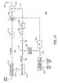
- FIG. 1illustrates a simplified block diagram of a transmitter apparatus 100 in accordance with one example embodiment.
- the transmitter 100comprises a data encoder and modulator 110 .
- the data encoder and modulator 110converts an input signal, for example a digital signal, to be transmitted to the modulation technique appropriate to the air interface standard in which the mobile device is operating.
- the data encoder and modulator 110uses CDMA modulation for use in an IS-2000 system.
- Other modulation schemesmay include, without limitation, Universal Mobile Telecommunications System (UMTS), 802.11, Global System for Mobile Communications (GSM), Enhanced Data rates for GSM Evolution (EDGE), Time division multiple access (TDMA), or others that are well known to those skilled in the art.
- UMTSUniversal Mobile Telecommunications System
- GSMGlobal System for Mobile Communications
- EDGEEnhanced Data rates for GSM Evolution
- TDMATime division multiple access
- the data encoder and modulator 110generates a Tx signal 145 and a data format/data rate indicator that uniquely indicates a supported combination of data rate, coding and modulation method of the mobile device, referred to herein as a data indicator “r” 150 .
- the Tx signal 145comprises data frames to be transmitted at variable data formats or data rates.
- the data indicator “r” 150indicates the variable data rate and format at which the signal is being transmitted.
- an explicit data rate signalsuch as the data indicator “r” 150 , need not be utilized.
- one or more components of the transmittercan be appropriately calibrated so that data rate and format information is implicitly taken into account during operation of the transmitter 100 . Different settings or calibrations can be utilized for different data rates, so that during a data rate change the settings or calibrations corresponding to the new data rate can be selected.
- the data encoder and modulator 110can be implemented using software, hardware or a combination of software and hardware.
- the Tx signal 145which can be a digital signal, is converted to an analog signal by a digital-to-analog converter 155 prior to performing analog processing.
- Analog processingcan include, for example, mixing to an intermediate frequency (IF) and filtering, as well as any other necessary analog processes. In some embodiments, zero IF is used and mixing to an intermediate frequency is not required.
- the amplitude of the analog processed signalis adjusted by an automatic gain control (AGC) amplifier 135 .
- the signalcan then be converted from an intermediate frequency signal (or zero intermediate frequency signal) to an RF frequency for transmission.
- the frequency conversion to an RF frequencyis done before the AGC amplifier 135 .
- the RF signalis input to an RF power amplifier 140 to generate a transmission signal, which is transmitted over the air interface by the antenna 160 .
- the AGC amplifier 135 and the RF power amplifier 140can be included in an amplifier stage of the transmitter.
- the data indicator “r” 150is mapped by the first mapper 115 to generate signal PAPR(r) 165 , which can be an effectively continuous signal.
- the signal PAPR(r) 165is the ratio of the peak signal power over the average signal power of Tx signal 145 that corresponds to the data indicator “r” 150 . This peak to average power ratio signal is designated as PAPR(r) 165 .
- PAPR(r) 165is in dB or proportional to dB.
- PAPR(r)can be scaled to any units that are suitable for the processor, hardware, or software as may be utilized in the particular embodiment.
- the first mapper 115can be implemented using hardware, software (for example using a look-up table, an array of values or the like), or a combination of hardware and software.
- a desired average transmit power block 125generates a desired average transmit power indicator “p” 170 .
- the desired average transmit power block 125uses one or more of an open loop power control method, a closed loop power control correction signal from the base station (e.g. transmitted every 1.25 ms), and other base station parameters for the offset of power.
- the desired average transmit power block 125can use the received total and pilot signal strengths of a base station signal received by the mobile device receiver and internal algorithms to estimate and adjust its own required transmit power. For example, if the received signal strength is high, then the desired average transmit power block 125 can determine that a lower transmit power may be sufficient. Likewise if the received signal strength is low, the desired average transmit power block 125 can determine that a larger transmit power may be required.
- a receiver(not shown) can be configured to receive base station signals and, based upon which, generate a received signal strength indicator for the desired average transmit power block 125 .
- the open loop transmit powers determined by the average transmit power block 125can further be adjusted, on a continuous basis, using closed loop power control commands transmitted by the base station to the mobile device receiver together with the received base station signals. These closed loop power control commands can instruct the desired average transmit power block 125 to make incremental adjustments to the transmit power calculated based on the received signal strength indicator. For example, the commands can be to increase, decrease or maintain transmit power.
- the desired average transmit power block 125can be configured to receive the closed loop power control commands from the mobile device receiver as well.
- the average desired transmit power block 125can be implemented using software, hardware or a combination of software and hardware.
- the desired average transmit power indicator “p” 170varies with time.
- average transmit power indicator “p” 170has units of dBm and is updated at the same rate as the closed loop power control (e.g., 1.25 ms).
- the two signals, PAPR(r) 165 and desired average transmit power indicator “p” 170are summed by a summer 175 that generates a peak power value in dBm (or proportional to it) representing the peak transmit power of the transmission signal expected at antenna 160 , which is the RF counterpart of Tx signal 145 at baseband.
- This peak transmit poweris mapped by the second mapper 120 to an effectively continuous “X” signal 180 , whose value is effectively continuous in a range that the second mapper 120 is designed for.
- the generation of signal X 180is as follows: for a given peak Tx power value, which is equal to p+PAPR(r), determine the corresponding optimal X signal 180 that gives the best transmitter power efficiency while still meeting the out of band spurious emissions and rho (waveform quality) requirements.
- An array of such values for the “X” signal 180is stored in the second mapper 120 . In one embodiment, this relationship is non-linear. Interpolation may be used in the mapping to get fine resolution and save storage memory. The array of such values for a transmitter may be determined by experimentation during calibration and testing of the transmitter.
- the second mapper 120 , the summer 175 , or both,can be implemented in hardware, software, or a combination of hardware and software.
- the first mapper 115 , second mapper 120 and summer 175may be included in an amplifier control block 111 of the transmitter (shown in FIG. 5 ), so that the amplifier control block 111 is configured to generate an amplifier control signal for adjusting at least one parameter of the amplifier stage.
- the first mapper 115 and second mapper 120can be used to determine the amplifier control signal based on peak to average power ratio and average transmit power of the RF transmission signal generated by the amplifier stage.
- one or more of the components of the transmitter 100can exhibit a stepped response during operation.
- a small change in the inputmay cause a jump in the output. This can occur as a result of, for example, but not limited to, a stage bypass, a load switch, a quiescent current step, or a quiescent current ramp that results from the small change to the input signal.
- one or more of the mappers 115 and 120may store more than one array or lookup table.
- the particular array or lookup table that is used in the mappers 115 and 120can depend on the input signal and the step response.
- the particular array or lookup table used in the mappers 115 and 120can be switched synchronously with the small change in the component input signal to anticipate the step response.
- the mappers 115 and 120can interpolate values falling between two different arrays or lookup tables. Again this can be performed synchronously with the small change in the component input signal to anticipate the step response. In this manner, one or more of mapper 115 and mapper 120 can be used to compensate for the stepped response of the respective component.
- the “X” signal 180is converted to an analog signal by a digital-to-analog (D/A) converter 185 and smoothed by a low pass filter LPF 190 .
- the output of the LPF 190is used to adjust a setting of the RF power amplifier 140 .
- the RF power amplifier 140includes or is otherwise coupled to a switched mode power supply and the setting adjusted by the “X” signal 180 is a supply voltage for the RF power amplifier 140 , which can be generated using the switched mode power supply in response to the level of the “X” signal 180 . Accordingly, the supply voltage “Y” 171 is supplied to a control input port of the RF power amplifier 140 , and is controllable in terms of its magnitude.
- the supply voltage “Y” 171is lowered or raised accordingly for optimal power efficiency in generating the power of the baseband Tx signal 145 and its radio frequency counterpart, the transmission signal radiated from antenna 160 .
- the setting adjusted by the “X” signal 180is a bias (i.e. quiescent) current for the RF power amplifier 140 , which can be generated using the switched mode power supply in a current mode.
- the desired average transmit power indicator “p” 170is also input to a gain control block 130 to generate an automatic gain control signal for controlling gain in the AGC amplifier 135 based on the average transmit power of the Tx signal 145 once amplified in the RF power amplifier 140 .
- the gain control block 130can be implemented using hardware, software (for example using a look-up table, an array of values or the like), or a combination of hardware and software.
- the delay of the Tx signal 145 to the output of antenna 160may be designed to be the same as the delay from desired average transmit power indicator “p” 170 or data indicator “r” 150 to the effects of “Y” 171 at antenna 160 .
- the signalsmay be referred as being delay aligned.
- “Y” 171can be time-advanced relative to the Tx signal 145 passing though D/A 185 and AGC amplifier 135 . In some embodiments this can be done to compensate for the finite time required for the RF power amplifier 140 to move its target outputs, for example when the supply voltage “Y” 171 is varied.
- the delay alignmentis implemented in software. In other embodiments, delay alignment can be implemented in hardware or a combination of hardware and software.
- FIG. 1Aillustrates an alternative embodiment of the transmitter apparatus 100 .
- the arrangement and configuration of the first mapper 115 , the second mapper 120 ′ and the summer 175has been modified.
- the first mapper 115remains coupled to the data encoder and modulator 110 to receive the data indicator “r” 150 and generate a signal representative of peak to average power ratio.
- the second mapper 120 ′is coupled directly to the desired average transmit power block 125 to receive the desired average transmit power indicator “p” 170 and generate a signal representative of average transmit power.
- the summer 175is coupled to the output of the first mapper 115 and the second mapper 120 ′, and generates “X” signal 180 to control a parameter of the RF power amplifier 140 .
- the first mapper 115 , the second mapper 120 ′, or both the first mapper 115 and the second mapper 120 ′can be re-written such that the influence of PAPR(r) 165 is introduced to “X” 180 at a different phase of the amplifier control block.
- the second mapper 120 ′may be configured specifically for the current operating PAPR, in which case the influence of the first mapper 115 can be correspondingly reduced.
- Second mapper 120 ′may include a plurality of different stored arrays or lookup tables corresponding to a plurality of different operating PAPR, such that a different “X” 180 signal is generated for each different operating PAPR in the plurality.
- the second mapper 120 ′may be configured as in FIG.
- first mapper 115can be modified to provide a correction factor for the DC-DC voltage, i.e. the supply voltage “Y” 171 of the RF power amplifier 140 (or corresponding amplifier control signal in either the analog or digital domain).
- multiple amplifier control signalscan be used.
- the amplifier control signalcan be or can control a bias current.
- the amplifier control signalcan be or can control a supply voltage.
- both a supply voltage and a bias currentcan be used as amplifier control signals.
- the one or more amplifier control signalscan be analog signals, digital signals or both analog and digital signals.
- one or more of the first mapper 115 , second mapper 120 ′ and summer 175can be implemented using hardware, software (for example using a look-up table, an array of values or the like), or a combination of hardware and software.
- FIG. 2illustrates an alternative embodiment of the transmitter apparatus 100 .
- the first mapper 115 and the summer 175 of the embodiment described with reference to FIG. 1are eliminated.
- the second mapper 120uses the desired average transmit power indicator “p” 170 as its input.
- the “X” signal 180is determined as follows: for a given desired average transmit power indicator “p” 170 , the corresponding optimal “X” signal 180 is generated that provides the best transmitter power efficiency while satisfying out of band spurious emissions and rho requirements.
- the second mapper 120can store a plurality of array or lookup table values that are specific to a given data rate or operating PAPR, such that a different array or lookup table is selected and implemented for a corresponding different data rate (or PAPR, which is dependent on data rate).
- the second mapper 120can generate the X signal 180 , as in the embodiments illustrated in FIGS. 1 and 1A , based on both peak to average power ratio and average transmit power, even though PAPR(r) 165 is not specifically provided to the second mapper 120 . Since PAPR can depend on data rate, by selecting a different array or lookup table to suit different PAPR, data rate is implicitly accounted for in the second mapper 120 .
- the values that are stored (e.g. in software) in the arrays and look-up tables implemented in second mapper 120may be determined experimentally as a way of calibrating the second mapper 120 for optimal power efficiency.
- the second mapper 120may also be configured to generate signal “X” 180 so as to compensate for different environmental factors or conditions (e.g. temperature) in which the transmitter 100 is operating. For example, a plurality of different array or table values can be determined experimentally corresponding to the particular environmental condition. During operation of the transmitter 100 , that environmental condition can be sensed and the appropriate array or look-up table can be loaded in the mapper 120 . Additionally, or alternatively, the second mapper 120 can be configured to compensate for prior knowledge of the transmitter operating conditions (e.g. frequency, drive band, etc), for example. In one embodiment, this is done in the digital domain. In variant embodiments, this can be done using analog methods, or a combination of digital and analog processing may be employed.
- different environmental factors or conditionse.g. temperature
- a plurality of different array or table valuescan be determined experimentally corresponding to the particular environmental condition.
- the second mapper 120can be configured to compensate for prior knowledge of the transmitter operating conditions (e.g. frequency, drive band, etc), for example. In one
- the stored array that is implemented by mapper 120may be continuously updated or substituted or interpolated at a rate appropriate to the changing environmental or operating conditions (e.g. temperature drift, cell handoff, data rate change) of the transmitter 100 . Accordingly, different suitable update rates for the second mapper 120 can be selected to fit the application or operating condition. Additional details pertaining to the embodiment described with reference to FIG. 2 are provided in the description above with respect to FIG. 1 .
- multiple control signalscan be used.
- the control signalcan be or can control a bias current.
- the control signalcan be or can control a supply voltage. In some embodiments, both a supply voltage and a bias current can be used as control signals.
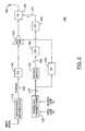
- FIG. 3illustrates another alternative embodiment of the transmitter apparatus 100 .
- This embodimentgenerates multiple “X” signals that are provided to adjust corresponding parts of the transmitter 100 or multiple parameters of the same part of the transmitter 100 , instead of just one “X” signal 180 to adjust only one parameter of the power amplifier 140 .
- the multiple “X” signalsmay be implemented by an array of second mappers 120 and 121 , D/A converters 185 and 186 , and low pass filters 190 and 191 .
- Each individual element of “X”is determined as described in the above embodiment.
- the multiple “X” signalscan be generated to provide the best transmitter power efficiency while still satisfying out of band spurious emissions and rho requirements.
- the corresponding mappermay be implemented as a threshold comparator.
- the multiple “X” signalsmay also include additional input variables such as the transmitter temperature and battery voltage.
- the second mapper 120then becomes multidimensional.
- Various simplified implementations (or approximations) of multidimensional mapping tablesmay also be used.
- FIG. 3shows only two second mappers 120 and 121 .
- the embodiments described hereinare not limited to any particular number of second mappers 120 .
- the embodiments described hereinare not to be limited to signal “X” 180 being an input to the RF power amplifier 140 , and instead signal “X” 180 can be used as a control input for other components of transmitter 100 .
- FIG. 3illustrates an embodiment similar to FIG. 1 , but multiple “X” signals are illustrated in FIG. 3 .
- the embodiments illustrated in FIGS. 1A and 2can similarly be modified to generate multiple “X” signals. Therefore, in some embodiments, the first mapper 115 shown in FIG. 3 is optional and may be omitted, in which case the second mapper 120 can be configured, as described above with reference to FIG. 2 , to be specific to a given data rate or operating PAPR. Environmental and operating conditions, for example, can also be compensated using the second mapper 120 as described above.
- FIG. 3Aillustrates an alternative embodiment of the transmitter apparatus 100 .
- the transmitter 100includes a gain control compensation block 195 for generating a gain correction factor for the gain control block 130 .
- the gain control compensation block 195is coupled to the outputs of LPF 190 and LPF 191 in a feedback loop with the gain control block 130 .
- the gain control compensation block 195compensates for gain expansion in the RF power amplifier 140 due to variation of the supply voltage “Y” 171 .
- the gain control compensation block 195can predict the gain of the RF power amplifier 140 based on the level of supply voltage “Y” 171 provided to the RF power amplifier 140 .
- the relationship between these two quantities due to the power amplifier gain expansioncan be either linear or non-linear.
- the gain control compensation block 195can then generate a gain correction factor, which is used to adjust (e.g. reduce) gain in the AGC amplifier 135 by an amount appropriate to offset the gain expansion in the RF power amplifier 140 predicted for that level of supply voltage. In this way, the output power of the transmission signal generated by the RF power amplifier 140 can be linearized with respect to the gain of the AGC amplifier 135 .
- the gain correction factorcan be fed back to the gain control block 130 in different ways.
- the gain correction factorcan be introduced as an adjustment to the desired average transmit power indicator “p” 170 , using a summer 197 located upstream of the gain control block 130 , to linearize the output of the power stage.
- the gain correction factorcan be combined with the automatic gain control signal generated by the gain control block 130 in a summer 196 located downstream of the gain control block 130 .
- the gain correction factorcan be provided as an input to the gain control block 130 , such that the gain control block 130 generates the automatic gain control signal based upon the combination of the average desired transmit power indicator “p” 170 and the gain correction factor.
- the hashed lines in FIG. 3Arepresent these different optional configurations.
- gain correction as described hereincan be performed in the analog domain, the digital domain or partially in each domain. Accordingly, one or more of the gain control compensation block 195 and summers 196 , 197 , individually or in any combination thereof, can be implemented using hardware, software (for example using a look-up table, an array of values or the like), or a combination of hardware and software.
- FIG. 4illustrates another alternative embodiment of the transmitter apparatus 100 .
- the second mapper 120is implemented by suitable analog hardware components and is included downstream of the D/A converter 185 .
- the functionality of the blocksremains otherwise as described herein, as does operation of the remainder of the transmitter.
- the implementation of the second mapper 120has been changed in this embodiment.
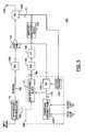
- FIG. 5illustrates another alternative embodiment of the transmitter apparatus 100 .
- the amplifier control block 111is explicitly illustrated in the transmitter 100 .
- the gain control compensation block 195is also illustrated.
- the amplifier control block 111receives the average transmit power indicator “p” 170 from the desired average transmit power block 125 and, optionally, the data indicator “r” 150 from the data encoder and modulator 110 .
- the amplifier control block 111is configured to receive both the average transmit power indicator “p” 170 and the data indicator “r” 150
- the amplifier control block 111is configured to receive the average transmit power indicator “p” 170 but not the data indicator “r” 150 .
- the amplifier control block 111generates and provides the “X” signal 180 to the D/A converter 185 .
- the amplifier control block 111can comprise at least one mapper used to generate the “X” signal 180 based on the average transmit power indicator “p” 170 . Whether or not the data indicator “r” 150 is explicitly provided, the amplifier control block 111 can further generate the “X” signal 180 based on a peak to average transmit power of the Tx signal 145 .
- the transmitter apparatus illustrated in FIGS. 1 , 1 A, 2 , 3 and 3 Adepict some of the different possible embodiments of the amplifier control block 111 .
- FIGS. 1 and 1Aillustrate embodiments in which the data indicator “r” 150 is explicitly provided
- FIG. 2illustrates embodiments where data rate information is accounted for implicitly within the configuration of the at least one mapper included in the amplifier control block 111 .
- FIGS. 3 and 3Aillustrate embodiments in which multiple second mappers 120 , 121 are incorporated to generate more than control signal for the RF power amplifier 140 .
- the amplifier control block 111can be implemented using hardware, software (for example using a look-up table, an array of values or the like), or a combination of hardware and software.
- the amplifier control block 111can be implemented on a programmable processing device, such as a microprocessor or microcontroller, Central Processing Unit (CPU), Digital Signal Processor (DSP), Field Programmable Gate Array (FPGA), general purpose processor, and the like.
- the programmable processing devicecan be coupled to program memory.
- Switched mode power supply 193is also shown explicitly in FIG. 5 .
- the switched mode power supply 193is coupled between the LPF 190 and the RF power amplifier 140 , though the switched mode power supply 193 could be included at other locations or incorporated into other components within the transmitter 100 .
- the switched mode power supply 193can be, for example, a DC-DC converter or some other voltage or current converter, which is configured to generate the supply voltage “Y” 171 in response to the “X” signal 180 .
- the “X” signal 180can be or can specify a pulse width or pulse density modulated signal, for example, to drive the switched mode power supply 193 .
- the amplifier control block 111can be included within the control system 199 , which can form an integrated controller for the transmitter 100 .
- the control system 199can generate hardware control signals for one or more of the physical components of the transmitter 100 based on one or more input signals, which can be provided by other components of the transmitter apparatus.
- At least one of the hardware control signals generated by the control system 199can be an amplifier control signal for adjusting at least one parameter of an amplifier stage included in the transmitter 100 , such as the supply voltage or bias current of the RF power amplifier 140 .
- the control system 199can generate the hardware control signals by defining a transfer function between the one or more input signals and the one or more control signals.
- the input-output transfer functioncan be defined by explicitly mapping input values to output values and storing that mapping in a lookup table or the like.
- the desired average transmit power block 125can also be included in the control system 199 , in which case one or both of the received signal strength indicator and the closed loop power control commands can be input signals to the control system 199 .
- the desired average transmit power block 125can be provided separately from the control system 199 and the average transmit power indicator “p” 170 can be provided as an input to the control system 199 .
- the one or more input signals provided to the control system 199can include at least one signal that is representative of the average transmit power of the Tx signal 145 .
- the data indicator “r” 150can also be provided as an input signal, in embodiments where the data indicator “r” 150 is explicitly available.
- data rate informationmay be embedded implicitly into the one or more mappers implemented in the amplifier control block 111 , in which case the data indicator “r” 150 may not be an input signal to the control system 199 (hence the dashed line). But in general, the control system 199 can generate the hardware control signals based on a peak to average power ratio of the Tx signal 145 , in addition to the average transmit power of the Tx signal 145 , and regardless of the availability of the data indicator “r” 150 .
- the gain control block 130can also be included in the control system 199 .
- the hardware control signals generated by the control system 199can also include the automatic gain control signal provided to the AGC amplifier 135 .
- the control system 199can further define an input-output transfer function between the one or more input signals and the automatic gain control signal.
- the gain control block 130can be omitted from the control system 199 and implemented as a separate hardware component in the transmitter 100 .
- the desired average transmit power block 125is included in the control system 199
- the average transmit power indicator “p” 170can be outputted from the control system 199 and provided to the gain control block 130 .
- the gain control compensation block 195can also be included in the control system 199 .
- the voltage supply signal “Y” 171can be one of the input signals to the control system 199 , and the input-output transfer function for the automatic gain control signal can be further defined in terms of the voltage supply signal “Y” 171 .
- some other signal generated internally within the control system 199such as the signal “X” 180 , which is representative of the power amplifier supply voltage can be used to adjust the automatic gain control signal. As described herein, the adjustment can be performed to compensate for gain expansion in the RF power amplifier 140 when the supply voltage is varied.
- the gain control compensation block 195can be omitted from the control system 199 and implemented as a separate hardware component in the transmitter 100 .
- control system 199can be implemented on one or more programmable processing devices, such as a microprocessor or microcontroller, Central Processing Unit (CPU), Digital Signal Processor (DSP), Field Programmable Gate Array (FPGA), general purpose processor, and the like.
- the programmable processing devicecan be coupled to program memory for implementing the functions of the control system 199 , and can have suitably configured input and output terminals or circuits for interfacing with the various hardware components of the transmitter 100 that are controlled using the programmable processing device.
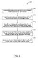
- FIG. 6illustrates acts of a method 200 for optimizing power efficiency in a transmitter apparatus in accordance with at least one embodiment. Some acts of the method 200 can be performed using hardware components, while other acts of the method 200 can be performed using software components. Some acts of the method 200 can be performed using both hardware and software components. Some acts of the method 200 can be performed alternatively using either hardware or software components, as will be described. Accordingly, the method 200 can be performed using software components only, hardware components only, or a combination of software and hardware components.
- an encoded and modulated transmit signal based on an input signalis generated.
- the input signalcan be a digital communication signal, such as a digitized voice signal or data signal, which is to be transmitted.
- the input signalcan be encoded and modulated using a communication standard employed by the transmitter.
- the modulation scheme usedcan be the CDMA modulation scheme, but could also be UMTS, GSM, EDGE, TDMA, or some other scheme.
- the encoding and modulatingcan be performed using hardware components, but could also be performed in software or some combination of the two.
- an analog representation of the encoded and transmitted signalis generated.
- a suitably configured digital to analog convertercan be used, for example.
- the analog representation of the encoded and modulated transmit signalis amplified in an amplifier stage to generate a transmission signal.
- the amplifier stagecan include an automatic gain control amplifier (e.g. 135 in FIG. 1 ) and an RF power amplifier (e.g. 140 in FIG. 1 ). This act can further comprise filtering and mixing the analog representation of the encoded and modulated signal with an intermediate frequency, prior to amplification in the amplifier stage.
- an amplifier control signalis generated based on a peak to average power ratio and an average transmit power of the transmission signal.
- Various approachescan be followed in order to generate the amplifier control signal.
- a type of the encoded and modulated transmit signalcan be mapped, using a first mapping function, to a first signal representation of the peak to average power ratio, and a second signal representative of the average transmit power of the transmission signal can be generated using a second mapper. The first and second signals can then be summed together to generate the amplifier control signal.
- mapping functioncorresponding to a different peak to average power ratio of the transmission signal, to generate the amplifier control signal. Accordingly, the desired average power of the transmission signal supplemented implicitly with peak to average power ratio information of the transmission signal (e.g. through selection of a given mapping function) can be mapped into the amplifier control signal.
- the act at 220can further comprise generating the amplifier control signal based on one or more environmental conditions in which the transmitter is operating, such as temperature, as well as one or more operating conditions of the transmitter, such as transmit frequency and drive band.
- the act at 220can be performed using one or more transistor logic circuits, one or more software components, comprising instructions executable by a processor and storable in memory for example, or some combination of hardware and software components.
- At 225at least one parameter of the amplifier stage is adjusted using the amplifier control signal.
- the amplifier control signalcan be or can control a supply voltage of the RF power amplifier, and can be generated at 220 so that the RF power amplifier operates efficiently while satisfying out of band and rho requirements.
- the method 200can further comprise generating an automatic gain control signal for controlling gain in the automatic gain control amplifier, which can be included in the amplifier stage in variant embodiments.
- the automatic gain control signalcan be generated based on the average transmit power of the transmission signal.
- the methodcan further comprise generating a gain correction factor based on the amplifier control signal, which is used to adjust the automatic gain control signal to compensate, as an example, for gain expansion in the RF power amplifier due to bias point variation.
- the method 200can comprise still further acts not explicitly shown in FIG. 6 , while in other embodiments one or more of the acts illustrated may be omitted or performed in a different order than as illustrated.
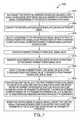
- FIG. 7illustrates acts of a method 250 for optimizing power efficiency in a transmitter apparatus in accordance with at least one embodiment.
- the acts of the method 250can be performed using hardware components, software components or a combination of hardware and software. Accordingly, the method 250 can also be performed using software components only, hardware components only, or a combination of software and hardware components.
- an encoded and modulated transmit signalis generated in a transmitter apparatus based on a digital input signal to be transmitted.
- the input signalcan be encoded and modulated using a communication standard employed by the transmitter.
- the modulation scheme usedcan be the CDMA modulation scheme, but could also be UMTS, GSM, EDGE, TDMA, or some other scheme.
- a data indicator corresponding to the encoded and modulated signalis also generated.
- the encoded and modulated signalis converted into an analog transmission signal.
- a suitably configured digital to analog convertercan be used.
- an output peak to average power ratio signal valueis selected from an array of different possible peak to average power ratio signal values.
- Each different peak to average power ratio signal valuescan correspond to a different data rate or data format, and the output peak to average power ratio signal value can be selected corresponding to the data indicator generated at 255 .
- the output peak to average power ratio signal value generated at 265can reflect the data rate or data format of the input digital signal.
- a desired transmit power level signal valuecan be generated.
- the desired average transmit power block 125(illustrated in FIG. 1 ) operating in closed or open loop mode can be used to generate the desired transmit power level signal.
- one or more of a received signal strength indicator and closed loop power control commandscan be used.
- an automatic gain control signalis generated based on the desired transmit power level signal value.
- the automatic gain control signalcan be generated, for example, so that the signal amplification provided by an automatic gain control amplifier (see e.g. 135 in FIG. 1 ) included in the transmitter apparatus causes a transmission signal to be generated at the desired average transmit power level.
- the desired transmit power level signal value and the peak to average power ratio signal valuecan be added together to generate a peak transmit power level signal value.
- the value of the peak transmit power level signal valuecan be mapped, essentially continuously, to a value for at least one control signal for at least one control device or element included in the transmitter apparatus.
- the control devicecan be a switched mode power supply (see e.g. 193 in FIG. 5 ) that controls a supply voltage for an RF power amplifier (see e.g. 140 in FIG. 1 ) included in the transmitter apparatus.
- the control values for the switched mode power supplycan be continuously mapped to achieve an optimized power efficiency in the RF power amplifier of the transmitter apparatus, while still meeting out of band spurious emissions and waveform quality requirements. This can be accomplished by ensuring that the supply voltage for the RF power amplifier is large enough to accommodate the peak transmit power level of the transmission signal with sufficient headroom.
- control value generated at 285is a digital signal
- the control signalcan be converted to an analog signal prior to being input into the control device.
- 290can be omitted from the method 250 .
- FIG. 8illustrates acts of a method 300 for optimizing power efficiency in a transmitter apparatus in accordance with at least one embodiment.
- Method 300can be performed entirely using software components. Some hardware components may be utilized as well, in variant embodiments.
- a signal representative of an average transmit power of a transmission signalis received.
- the representative signalcan be provided to an input terminal of a processor.
- an amplifier control signalis determined by mapping the average transmit power and a peak to average power ratio of the transmission signal to a control value for an amplifier stage, which can include an automatic gain control amplifier (see e.g. 135 in FIG. 5 ) and an RF power amplifier (see e.g. 140 in FIG. 5 ).
- the mappingcan be encoded in one or more lookup tables or the like, implemented in memory coupled to the processor.
- the average power ratio of the transmission signalcan be embedded within the one or more lookup tables, for example, in the case where a different lookup table is implemented for each of a number of different possible average power ratios.
- a signal representative of an average power ratiocan be received, for example, at a second input terminal of the processor, and then used to modify values stored in the one or more lookup tables according to the average power ratio of the transmission signal.
- the amplifier control signal generated at 310is provided to the amplifier stage to adjust at least one parameter of the amplifier stage according to the control value.
- an output terminal of the processorcan carry the amplifier control signal to the amplifier stage or, perhaps, some other element coupled intermediately between the processor and the amplifier stage.
- the amplifier control signalcan be provided to a switched mode power supply coupled to the RF power amplifier, and the value of the amplifier control signal can specify a supply voltage for the RF power amplifier.
- signals Xmay control various devices within the transmitter, including one or more power amplifiers, one or more stages of a power amplifier, one or more drive amplifiers, one or more AGC amplifiers, one or more power supplies for a power amplifier and/or other devices in a transmitter, one or more power supplies for other devices on components, one or more mixers, one or more matching networks, one or more filters, one or more power couplers or switches, one or more charging circuits, one or more voltage or current sources, one or more voltage or current regulators, one or more voltage or current converters, and any combination of these components.
- inputs such as the multiple X signals, to control certain transmitter circuit parametersmay include (but are not limited to): (a) bias to each or some of the amplifying devices inside a power amplifier so that only the minimum bias is provided to obtain the required out of band spurious emissions and rho for each given transmitted power and/or PAPR values in the supported range; (b) power supply voltage(s) to all or selected stages of an RF power amplifier and/or other circuits in the transmitter apparatus; such power supply voltages are supplied to the circuits so that only the minimum voltage is provided to obtain the required out of band spurious emissions and rho for each given transmitted power and/or PAPR values in the supported range; (c) to switch in or out, or turn on or off selected stages according to the transmitted power and/or PAPR values; and (d) gains of all or selected components of the amplifier stage in the transmitter; (e) conducting angle of all or selected components of the amplifier stage in the transmitter; (f) class of amplifying (e.g., Class A, AB,
- At least some of the embodiments of the transmitter apparatus and power optimization method described hereinprovide improved power efficiency of transmitters having varying transmit power and high/variable PAPR. This may, for example, provide a mobile, battery-powered device with increased battery life performance.
Landscapes
- Engineering & Computer Science (AREA)
- Power Engineering (AREA)
- Computer Networks & Wireless Communication (AREA)
- Signal Processing (AREA)
- Amplifiers (AREA)
- Transmitters (AREA)
Abstract
Description
Claims (20)
Priority Applications (1)
| Application Number | Priority Date | Filing Date | Title |
|---|---|---|---|
| US13/829,569US8873675B2 (en) | 2002-12-02 | 2013-03-14 | Method and apparatus for optimizing transmitter power efficiency |
Applications Claiming Priority (5)
| Application Number | Priority Date | Filing Date | Title |
|---|---|---|---|
| US43029302P | 2002-12-02 | 2002-12-02 | |
| US10/724,951US7471738B2 (en) | 2002-12-02 | 2003-12-01 | Method and apparatus for optimizing transmitter power efficiency |
| US12/276,650US7852968B2 (en) | 2002-12-02 | 2008-11-24 | Method and apparatus for optimizing transmitter power efficiency |
| US12/784,932US8428181B2 (en) | 2002-12-02 | 2010-05-21 | Method and apparatus for optimizing transmitter power efficiency |
| US13/829,569US8873675B2 (en) | 2002-12-02 | 2013-03-14 | Method and apparatus for optimizing transmitter power efficiency |
Related Parent Applications (1)
| Application Number | Title | Priority Date | Filing Date |
|---|---|---|---|
| US12/784,932ContinuationUS8428181B2 (en) | 2002-12-02 | 2010-05-21 | Method and apparatus for optimizing transmitter power efficiency |
Publications (2)
| Publication Number | Publication Date |
|---|---|
| US20130273863A1 US20130273863A1 (en) | 2013-10-17 |
| US8873675B2true US8873675B2 (en) | 2014-10-28 |
Family
ID=44263154
Family Applications (2)
| Application Number | Title | Priority Date | Filing Date |
|---|---|---|---|
| US12/784,932Expired - Fee RelatedUS8428181B2 (en) | 2002-12-02 | 2010-05-21 | Method and apparatus for optimizing transmitter power efficiency |
| US13/829,569Expired - LifetimeUS8873675B2 (en) | 2002-12-02 | 2013-03-14 | Method and apparatus for optimizing transmitter power efficiency |
Family Applications Before (1)
| Application Number | Title | Priority Date | Filing Date |
|---|---|---|---|
| US12/784,932Expired - Fee RelatedUS8428181B2 (en) | 2002-12-02 | 2010-05-21 | Method and apparatus for optimizing transmitter power efficiency |
Country Status (4)
| Country | Link |
|---|---|
| US (2) | US8428181B2 (en) |
| EP (1) | EP2388914B1 (en) |
| CN (1) | CN102255620B (en) |
| CA (1) | CA2740489C (en) |
Families Citing this family (20)
| Publication number | Priority date | Publication date | Assignee | Title |
|---|---|---|---|---|
| US8428181B2 (en) | 2002-12-02 | 2013-04-23 | Research In Motion Limited | Method and apparatus for optimizing transmitter power efficiency |
| US7333563B2 (en) | 2004-02-20 | 2008-02-19 | Research In Motion Limited | Method and apparatus for improving power amplifier efficiency in wireless communication systems having high peak to average power ratios |
| US8761305B2 (en) | 2006-06-14 | 2014-06-24 | Blackberry Limited | Input drive control for switcher regulated power amplifier modules |
| US7873119B2 (en)* | 2006-06-14 | 2011-01-18 | Research In Motion Limited | Input drive control for switcher regulated power amplifier modules |
| KR101010042B1 (en)* | 2006-06-14 | 2011-01-21 | 리서치 인 모션 리미티드 | Improved Control of Switcher-Adjusted Power Amplifier Modules |
| US8620238B2 (en) | 2010-07-23 | 2013-12-31 | Blackberry Limited | Method of power amplifier switching power control using post power amplifier power detection |
| US8514918B2 (en)* | 2010-09-24 | 2013-08-20 | Intel Corporation | Close-loop power transmission calibration |
| US9031601B2 (en) | 2012-06-25 | 2015-05-12 | Telefonaktiebolaget L M Ericsson (Publ) | Controlling radio transmitter power based on signal performance |
| US8787851B2 (en) | 2012-07-10 | 2014-07-22 | Huawei Device Co., Ltd. | System and method for quickly power amplifier control |
| US9497058B2 (en)* | 2012-11-26 | 2016-11-15 | Aviacomm Inc. | High efficiency adaptive RF transmitter |
| US9480017B2 (en)* | 2013-02-11 | 2016-10-25 | Qualcomm Incorporated | Dynamic power management control |
| US9059877B2 (en) | 2013-05-31 | 2015-06-16 | Qualcomm Incorporated | Dynamic gain for DAC illumination control |
| US20160149733A1 (en)* | 2014-11-26 | 2016-05-26 | Applied Materials, Inc. | Control architecture for devices in an rf environment |
| US9872341B2 (en) | 2014-11-26 | 2018-01-16 | Applied Materials, Inc. | Consolidated filter arrangement for devices in an RF environment |
| TWI631820B (en)* | 2015-02-15 | 2018-08-01 | 西凱渥資訊處理科技公司 | Unpowered switch module |
| US10142943B2 (en)* | 2016-06-14 | 2018-11-27 | Qualcomm Incorporated | Techniques and apparatuses for peak to average ratio (PAR) based power management |
| CN107872865B (en)* | 2016-09-24 | 2019-05-17 | 上海朗帛通信技术有限公司 | Method and apparatus for adjusting transmit power in UE and base station |
| US10419066B1 (en)* | 2017-10-05 | 2019-09-17 | Harmonic, Inc. | Remote radio frequency (RF) AGC loop |
| US11901921B2 (en)* | 2020-11-02 | 2024-02-13 | Nokia Solutions And Networks Oy | Radio apparatus |
| US20230319736A1 (en)* | 2022-03-11 | 2023-10-05 | Apple Inc. | Method for multiple power class support |
Citations (96)
| Publication number | Priority date | Publication date | Assignee | Title |
|---|---|---|---|---|
| US3486128A (en) | 1968-02-07 | 1969-12-23 | Us Army | Power amplifier for amplitude modulated transmitter |
| US4453264A (en) | 1982-09-23 | 1984-06-05 | Hochstein Peter A | Amplifier power supply controlled by audio signal |
| EP0171843A2 (en) | 1984-08-17 | 1986-02-19 | Philips Electronics Uk Limited | Bipolar transistor RF power amplifier |
| US4809339A (en) | 1985-09-12 | 1989-02-28 | Kelvin Shih | Audio transducer |
| US4849711A (en) | 1987-09-04 | 1989-07-18 | Digital Equipment Corporation | Automatic gain control system |
| US5192919A (en) | 1991-10-03 | 1993-03-09 | Motorola, Inc. | Transmitter having a temperature adjusted power amplifier |
| US5267262A (en) | 1989-11-07 | 1993-11-30 | Qualcomm Incorporated | Transmitter power control system |
| JPH0669002B2 (en) | 1986-05-23 | 1994-08-31 | 日本電信電話株式会社 | High frequency amplifier |
| US5452473A (en) | 1994-02-28 | 1995-09-19 | Qualcomm Incorporated | Reverse link, transmit power correction and limitation in a radiotelephone system |
| US5467058A (en) | 1993-09-01 | 1995-11-14 | Yamaha Corporation | Amplifier circuit with a stabilized bias in its output stage |
| US5485486A (en) | 1989-11-07 | 1996-01-16 | Qualcomm Incorporated | Method and apparatus for controlling transmission power in a CDMA cellular mobile telephone system |
| US5732334A (en) | 1996-07-04 | 1998-03-24 | Mitsubishi Denki Kabushiki Kaisha | Radio transmitter and method of controlling transmission by radio transmitter |
| US5852630A (en) | 1997-07-17 | 1998-12-22 | Globespan Semiconductor, Inc. | Method and apparatus for a RADSL transceiver warm start activation procedure with precoding |
| EP0977354A1 (en) | 1998-02-19 | 2000-02-02 | Ntt Mobile Communications Network Inc. | Amplifier for radio transmission |
| US6043707A (en) | 1999-01-07 | 2000-03-28 | Motorola, Inc. | Method and apparatus for operating a radio-frequency power amplifier as a variable-class linear amplifier |
| US6064269A (en) | 1998-07-31 | 2000-05-16 | Motorola, Inc. | Power amplifier with variable input voltage source |
| US6107878A (en) | 1998-08-06 | 2000-08-22 | Qualcomm Incorporated | Automatic gain control circuit for controlling multiple variable gain amplifier stages while estimating received signal power |
| US6137840A (en) | 1995-03-31 | 2000-10-24 | Qualcomm Incorporated | Method and apparatus for performing fast power control in a mobile communication system |
| US6166598A (en) | 1999-07-22 | 2000-12-26 | Motorola, Inc. | Power amplifying circuit with supply adjust to control adjacent and alternate channel power |
| US6178313B1 (en) | 1998-12-31 | 2001-01-23 | Nokia Mobile Phones Limited | Control of gain and power consumption in a power amplifier |
| US6205127B1 (en) | 1998-04-21 | 2001-03-20 | Lucent Technologies, Inc. | Wireless telecommunications system that mitigates the effect of multipath fading |
| US6208202B1 (en) | 1998-09-22 | 2001-03-27 | Qualcomm, Inc | High efficiency switched gain power amplifier |
| WO2000077950A8 (en) | 1999-06-14 | 2001-04-19 | Qualcomm Inc | Adjusting maximum transmit power to maintain constant margin for adjacent channel power rejection |
| US6252455B1 (en) | 1999-10-07 | 2001-06-26 | Motorola, Inc. | Method and apparatus for efficient signal amplification |
| DE10002523A1 (en) | 2000-01-21 | 2001-08-02 | Infineon Technologies Ag | Circuit arrangement for regulating the transmission power of a battery-operated radio |
| US20010026600A1 (en) | 2000-03-31 | 2001-10-04 | Mitsubishi Denki Kabushiki Kaisha | Radio transmitter with reduced power consumption |
| US6313698B1 (en) | 1999-09-24 | 2001-11-06 | Qualcomm Incorporated | Method and apparatus for wireless phone transmit power amplification with reduced power consumption |
| US20020013157A1 (en) | 2000-06-13 | 2002-01-31 | Matsushita Electric Industrial Co., Ltd. | Radio communications apparatus and transmission power control method thereof |
| US6349216B1 (en) | 1999-07-22 | 2002-02-19 | Motorola, Inc. | Load envelope following amplifier system |
| US6359504B1 (en) | 2000-01-28 | 2002-03-19 | Lucent Technologies Inc. | Power amplifier using upstream signal information |
| US6373823B1 (en) | 1999-01-28 | 2002-04-16 | Qualcomm Incorporated | Method and apparatus for controlling transmission power in a potentially transmission gated or capped communication system |
| US20020080887A1 (en) | 2000-10-20 | 2002-06-27 | Young-Ho Jeong | In-band adjacent-channel digital audio broadcasting system |
| US6421327B1 (en) | 1999-06-28 | 2002-07-16 | Qualcomm Incorporated | Method and apparatus for controlling transmission energy in a communication system employing orthogonal transmit diversity |
| WO2002060088A1 (en) | 2000-11-02 | 2002-08-01 | Conexant Systems, Inc. | Continuous closed-loop power control system including modulation injection in a wireless transceiver power amplifier |
| US6445247B1 (en) | 2001-06-01 | 2002-09-03 | Qualcomm Incorporated | Self-controlled high efficiency power amplifier |
| WO2002076057A1 (en) | 2001-03-16 | 2002-09-26 | Skyworks Solutions, Inc. | Dynamically varying linearity system for an rf front-end of a communication device |
| US20020183028A1 (en) | 1999-12-28 | 2002-12-05 | Hideyuki Takahashi | Receiving Apparatus And Gain Controlling Method |
| WO2002033844A3 (en) | 2000-10-18 | 2002-12-19 | Ericsson Telefon Ab L M | Communications systems |
| US20030002452A1 (en) | 2001-06-26 | 2003-01-02 | Sahota Gurkanwal Singh | System and method for power control calibration and a wireless communication device |
| US20030036361A1 (en) | 1999-12-24 | 2003-02-20 | Hiroyuki Kawai | Method and device for transmitting burst signal in mobile communication system, information distribution method, and information distribution controller |
| US6525605B2 (en) | 1998-08-19 | 2003-02-25 | Harris Corporation | Power amplifier system having frequency and amplifier failure compensation |
| US6531860B1 (en) | 2001-06-14 | 2003-03-11 | Qualcomm Inc. | Integrated power detector with temperature compensation |
| US6535066B1 (en) | 2001-06-21 | 2003-03-18 | Cisco Technology, Inc. | Dynamic RF amplifier bias control for digital wireless communications devices |
| US20030060193A1 (en) | 2000-04-25 | 2003-03-27 | Hiroyuki Kurita | Apparatus, method and program for communication test, and recorded medium on which that program has been recorded |
| US20030086398A1 (en) | 2001-11-06 | 2003-05-08 | Kimmo Hiltunen | Method and arrangement in a communication system |
| US6566944B1 (en) | 2002-02-21 | 2003-05-20 | Ericsson Inc. | Current modulator with dynamic amplifier impedance compensation |
| US6597925B1 (en) | 2000-03-16 | 2003-07-22 | Agere Systems Inc. | Transmitter circuit with frequency self-optimization |
| US20030176202A1 (en) | 2002-03-07 | 2003-09-18 | Siemens Information And Communication Mobile Llc | Combined open and closed loop power control with differential measurement |
| US20030222819A1 (en) | 1996-09-09 | 2003-12-04 | Tracbeam Llc. | Locating a mobile station using a plurality of wireless networks and applications therefor |
| JP2004048797A (en) | 2003-09-12 | 2004-02-12 | Hitachi Ltd | Transmitter and power amplifier |
| US20040100921A1 (en) | 2002-11-27 | 2004-05-27 | Farooq Ullah Khan | Time-orthogonal CDMA wireless communication system |
| WO2004051843A2 (en) | 2002-12-02 | 2004-06-17 | Research In Motion Limited | Method and apparatus for optimizing transmitter power efficiency |
| US6765440B2 (en) | 2002-12-18 | 2004-07-20 | Andrew Corporation | Model-based feed-forward linearization of amplifiers |
| EP1441472A2 (en) | 2003-01-22 | 2004-07-28 | Hong Kong Applied Science and Technology Research Institute Co. Ltd. | Wireless local area network time division duplex relay system with high speed automatic up-link and down-link detection |
| US20040180686A1 (en) | 2002-02-21 | 2004-09-16 | Takashi Nakayama | Transmission output circuit and mobile communication terminal |
| US20040213335A1 (en) | 2003-04-23 | 2004-10-28 | Francis Forest | Apparatus and method for mobile communication device transmission |
| US20040251962A1 (en) | 2003-06-10 | 2004-12-16 | Nokia Corporation | Power control for a switching mode power amplifier |
| KR20050013782A (en) | 2003-07-29 | 2005-02-05 | 매그나칩 반도체 유한회사 | Electrically erasable and programmable read only memory |
| US6862457B1 (en) | 2000-06-21 | 2005-03-01 | Qualcomm Incorporated | Method and apparatus for adaptive reverse link power control using mobility profiles |
| US6876697B2 (en) | 2000-12-12 | 2005-04-05 | Sierra Wireless, Inc. | Apparatus and method for power ramp up of wireless modem transmitter |
| US6891902B2 (en) | 2002-07-02 | 2005-05-10 | Intel Corporation | System and method for adjusting a power level of a transmission signal |
| US6898257B2 (en) | 2000-02-28 | 2005-05-24 | Lucent Technologies Inc. | Transmitter device having a modulation closed loop |
| US20050122171A1 (en) | 2003-12-08 | 2005-06-09 | Osamu Miki | Power source circuit for high frequency power amplifying circuit and semiconductor integrated circuit for power source and electronics component for power source |
| WO2005053151A1 (en) | 2003-11-20 | 2005-06-09 | Northrop Grumman Corporation | Variable supply amplifier system |
| US6914487B1 (en) | 2002-04-19 | 2005-07-05 | National Semiconductor Corporation | Method and system for providing power management in a radio frequency power amplifier using adaptive envelope tracking |
| JP2005197870A (en) | 2004-01-05 | 2005-07-21 | Fujitsu Ltd | Distortion compensation power amplifier |
| US20050186923A1 (en) | 2004-02-20 | 2005-08-25 | Research In Motion Limited | Method and apparatus for improving power amplifier efficiency in wireless communication systems having high peak to average power ratios |
| JP2005244996A (en) | 2004-02-27 | 2005-09-08 | Research In Motion Ltd | Method and apparatus for optimizing transmitter power efficiency |
| US6965676B1 (en) | 1999-10-19 | 2005-11-15 | Texas Instruments Incorporated | Volume-responsive loudness compensation circuits, systems, and methods |
| US20050285681A1 (en) | 2004-06-25 | 2005-12-29 | Mark Doherty | Power amplifier (pa) efficiency with low current dc to dc converter |
| US6985704B2 (en) | 2002-05-01 | 2006-01-10 | Dali Yang | System and method for digital memorized predistortion for wireless communication |
| US20060046658A1 (en) | 2002-09-05 | 2006-03-02 | Cruz Rene L | Scheduling methods for wireless networks |
| US20060046666A1 (en) | 2003-10-07 | 2006-03-02 | Matsushita Electric Industrial Co., Ltd. | Transmission device, transmission output control method, and radio communication device |
| US7023897B2 (en)* | 2000-12-20 | 2006-04-04 | Nec Corporation | Transmission circuit |
| EP1569330B1 (en) | 2004-02-20 | 2006-05-03 | Research In Motion Limited | Method and apparatus for improving power amplifier efficience in wireless communication systems having high peak to average power ratios |
| US20060140296A1 (en) | 2001-12-14 | 2006-06-29 | Samsung Electronics Co., Ltd. | Apparatus and method for reducing the peak-to-average power ratio of OFDM/OFDMA signals |
| US7116955B2 (en) | 2002-09-24 | 2006-10-03 | Ati Technologies, Inc. | Dual loop automatic gain control |
| US20070035285A1 (en) | 2002-01-17 | 2007-02-15 | Balu Balakrishnan | Methods and apparatus for maintaining an approximate constant current output characteristic in a switched mode power supply |
| WO2007054609A1 (en) | 2005-11-10 | 2007-05-18 | Nokia Corporation | Method and arrangement for optimizing efficiency of a power amplifier |
| US20070139014A1 (en) | 2001-10-11 | 2007-06-21 | Andrew Girson | Method and apparatus for optimizing performance and battery life of electronic devices based on system and application parameters |
| CN1329413C (en) | 2006-01-23 | 2007-08-01 | 南京医科大学 | Antibody for treating or preventing senile dementia, its expression vector and application in drug preparation |
| US20070184791A1 (en) | 2006-02-03 | 2007-08-09 | Vikas Vinayak | Power amplifier controller circuit |
| US20070258602A1 (en) | 2006-05-05 | 2007-11-08 | Nokia Corporation | Method and arrangement for optimizing efficiency of a power amplifier |
| US20070291718A1 (en) | 2006-06-14 | 2007-12-20 | Research In Motion Limited | Control of switcher regulated power amplifier modules |
| US20070291872A1 (en) | 2006-06-14 | 2007-12-20 | Research In Motion Limited | Input drive control for switcher regulated power amplifier modules |
| US7375540B2 (en) | 2002-12-02 | 2008-05-20 | Broadcom Corporation | Process monitor for monitoring and compensating circuit performance |
| US7411896B1 (en) | 2001-08-29 | 2008-08-12 | Ostendo Technologies, Inc. | Method, apparatus, and system for power amplifier efficiency improvement |
| US20090021303A1 (en) | 2007-07-17 | 2009-01-22 | Vikas Vinayak | Distortion-Driven Power Amplifier Power Supply Controller |
| US7542741B2 (en) | 2006-01-31 | 2009-06-02 | Skyworks Solutions, Inc. | System and method for power mapping to compensate for power amplifier gain control variations |
| US20100283626A1 (en) | 2002-06-11 | 2010-11-11 | Intelligent Technologies International, Inc. | Coastal Monitoring Techniques |
| US7877566B2 (en) | 2005-01-25 | 2011-01-25 | Atmel Corporation | Simultaneous pipelined read with multiple level cache for improved system performance using flash technology |
| US20110130105A1 (en) | 2002-12-02 | 2011-06-02 | Research In Motion Limited | Method and apparatus for optimizing transmitter power efficiency |
| JP2004500775A5 (en) | 2001-03-02 | 2011-09-15 | ||
| CA2745491A1 (en) | 2010-07-23 | 2012-01-23 | Research In Motion Limited | Method of power amplifier switching power control using post power amplifier power detection |
| US20120021704A1 (en) | 2010-07-23 | 2012-01-26 | Research In Motion Limited | Method of power amplifier switching power control using post power amplifier power detection |
| US20130005286A1 (en) | 2006-06-14 | 2013-01-03 | Research In Motion Limited | Input drive control for switcher regulated power amplifier modules |
Family Cites Families (6)
| Publication number | Priority date | Publication date | Assignee | Title |
|---|---|---|---|---|
| JPH01155041A (en) | 1987-12-11 | 1989-06-16 | Hitachi Ltd | Cylinder inflow gas quantity compensating method |
| JPH0669002A (en) | 1992-08-21 | 1994-03-11 | Nippondenso Co Ltd | Positive temperature coefficient characteristic thermistor |
| JP3136382B2 (en) | 1992-10-19 | 2001-02-19 | 京セラ株式会社 | Linear transmitter |
| JPH06252797A (en) | 1993-02-23 | 1994-09-09 | Sony Corp | Transmitter-receiver |
| DE69622808T2 (en) | 1995-09-29 | 2003-03-27 | Kabushiki Kaisha Toshiba, Kawasaki | Control rod drive mechanism |
| US6721368B1 (en) | 2000-03-04 | 2004-04-13 | Qualcomm Incorporated | Transmitter architectures for communications systems |
- 2010
- 2010-05-21USUS12/784,932patent/US8428181B2/ennot_activeExpired - Fee Related
- 2011
- 2011-05-17CACA2740489Apatent/CA2740489C/enactiveActive
- 2011-05-18EPEP11166623.6Apatent/EP2388914B1/enactiveActive
- 2011-05-20CNCN201110133089.5Apatent/CN102255620B/enactiveActive
- 2013
- 2013-03-14USUS13/829,569patent/US8873675B2/ennot_activeExpired - Lifetime
Patent Citations (167)
| Publication number | Priority date | Publication date | Assignee | Title |
|---|---|---|---|---|
| US3486128A (en) | 1968-02-07 | 1969-12-23 | Us Army | Power amplifier for amplitude modulated transmitter |
| US4453264A (en) | 1982-09-23 | 1984-06-05 | Hochstein Peter A | Amplifier power supply controlled by audio signal |
| EP0171843A2 (en) | 1984-08-17 | 1986-02-19 | Philips Electronics Uk Limited | Bipolar transistor RF power amplifier |
| US4809339A (en) | 1985-09-12 | 1989-02-28 | Kelvin Shih | Audio transducer |
| JPH0669002B2 (en) | 1986-05-23 | 1994-08-31 | 日本電信電話株式会社 | High frequency amplifier |
| US4849711A (en) | 1987-09-04 | 1989-07-18 | Digital Equipment Corporation | Automatic gain control system |
| US5267262A (en) | 1989-11-07 | 1993-11-30 | Qualcomm Incorporated | Transmitter power control system |
| US5485486A (en) | 1989-11-07 | 1996-01-16 | Qualcomm Incorporated | Method and apparatus for controlling transmission power in a CDMA cellular mobile telephone system |
| US5192919A (en) | 1991-10-03 | 1993-03-09 | Motorola, Inc. | Transmitter having a temperature adjusted power amplifier |
| US5467058A (en) | 1993-09-01 | 1995-11-14 | Yamaha Corporation | Amplifier circuit with a stabilized bias in its output stage |
| US5452473A (en) | 1994-02-28 | 1995-09-19 | Qualcomm Incorporated | Reverse link, transmit power correction and limitation in a radiotelephone system |
| US6137840A (en) | 1995-03-31 | 2000-10-24 | Qualcomm Incorporated | Method and apparatus for performing fast power control in a mobile communication system |
| US5732334A (en) | 1996-07-04 | 1998-03-24 | Mitsubishi Denki Kabushiki Kaisha | Radio transmitter and method of controlling transmission by radio transmitter |
| US20030222819A1 (en) | 1996-09-09 | 2003-12-04 | Tracbeam Llc. | Locating a mobile station using a plurality of wireless networks and applications therefor |
| US5852630A (en) | 1997-07-17 | 1998-12-22 | Globespan Semiconductor, Inc. | Method and apparatus for a RADSL transceiver warm start activation procedure with precoding |
| EP0977354A1 (en) | 1998-02-19 | 2000-02-02 | Ntt Mobile Communications Network Inc. | Amplifier for radio transmission |
| US6265935B1 (en) | 1998-02-19 | 2001-07-24 | Ntt Mobile Communications Network Inc. | Amplifier for radio transmission |
| US6205127B1 (en) | 1998-04-21 | 2001-03-20 | Lucent Technologies, Inc. | Wireless telecommunications system that mitigates the effect of multipath fading |
| US6064269A (en) | 1998-07-31 | 2000-05-16 | Motorola, Inc. | Power amplifier with variable input voltage source |
| US6107878A (en) | 1998-08-06 | 2000-08-22 | Qualcomm Incorporated | Automatic gain control circuit for controlling multiple variable gain amplifier stages while estimating received signal power |
| US6525605B2 (en) | 1998-08-19 | 2003-02-25 | Harris Corporation | Power amplifier system having frequency and amplifier failure compensation |
| US6208202B1 (en) | 1998-09-22 | 2001-03-27 | Qualcomm, Inc | High efficiency switched gain power amplifier |
| US6178313B1 (en) | 1998-12-31 | 2001-01-23 | Nokia Mobile Phones Limited | Control of gain and power consumption in a power amplifier |
| US6043707A (en) | 1999-01-07 | 2000-03-28 | Motorola, Inc. | Method and apparatus for operating a radio-frequency power amplifier as a variable-class linear amplifier |
| US6373823B1 (en) | 1999-01-28 | 2002-04-16 | Qualcomm Incorporated | Method and apparatus for controlling transmission power in a potentially transmission gated or capped communication system |
| CN1355967A (en) | 1999-06-14 | 2002-06-26 | 高通股份有限公司 | Adjusting maximum transmit power to maintain constant margin for adjacement channel power |
| WO2000077950A8 (en) | 1999-06-14 | 2001-04-19 | Qualcomm Inc | Adjusting maximum transmit power to maintain constant margin for adjacent channel power rejection |
| US6421327B1 (en) | 1999-06-28 | 2002-07-16 | Qualcomm Incorporated | Method and apparatus for controlling transmission energy in a communication system employing orthogonal transmit diversity |
| US6166598A (en) | 1999-07-22 | 2000-12-26 | Motorola, Inc. | Power amplifying circuit with supply adjust to control adjacent and alternate channel power |
| US6349216B1 (en) | 1999-07-22 | 2002-02-19 | Motorola, Inc. | Load envelope following amplifier system |
| US6313698B1 (en) | 1999-09-24 | 2001-11-06 | Qualcomm Incorporated | Method and apparatus for wireless phone transmit power amplification with reduced power consumption |
| US6252455B1 (en) | 1999-10-07 | 2001-06-26 | Motorola, Inc. | Method and apparatus for efficient signal amplification |
| US6965676B1 (en) | 1999-10-19 | 2005-11-15 | Texas Instruments Incorporated | Volume-responsive loudness compensation circuits, systems, and methods |
| US20030036361A1 (en) | 1999-12-24 | 2003-02-20 | Hiroyuki Kawai | Method and device for transmitting burst signal in mobile communication system, information distribution method, and information distribution controller |
| US20020183028A1 (en) | 1999-12-28 | 2002-12-05 | Hideyuki Takahashi | Receiving Apparatus And Gain Controlling Method |
| DE10002523A1 (en) | 2000-01-21 | 2001-08-02 | Infineon Technologies Ag | Circuit arrangement for regulating the transmission power of a battery-operated radio |
| US20010048292A1 (en) | 2000-01-21 | 2001-12-06 | Martin Wahl | Circuit configuration for controlling the transmitting power of a battery-operated transceiver |
| JP2001237722A (en) | 2000-01-21 | 2001-08-31 | Infineon Technologies Ag | Transmission power adjustment circuit device |
| US6871050B2 (en) | 2000-01-21 | 2005-03-22 | Infineon Technologies Ag | Circuit configuration for controlling the transmitting power of a battery-operated transceiver |
| US6359504B1 (en) | 2000-01-28 | 2002-03-19 | Lucent Technologies Inc. | Power amplifier using upstream signal information |
| US6898257B2 (en) | 2000-02-28 | 2005-05-24 | Lucent Technologies Inc. | Transmitter device having a modulation closed loop |
| US6597925B1 (en) | 2000-03-16 | 2003-07-22 | Agere Systems Inc. | Transmitter circuit with frequency self-optimization |
| CN1153388C (en) | 2000-03-31 | 2004-06-09 | 三菱电机株式会社 | Wireless Transmitter with Low Power Consumption |
| EP1146636A1 (en) | 2000-03-31 | 2001-10-17 | Mitsubishi Denki Kabushiki Kaisha | Radio transmitter with reduced power consumption |
| JP2001284998A (en) | 2000-03-31 | 2001-10-12 | Mitsubishi Electric Corp | Wireless transmission device |
| US20010026600A1 (en) | 2000-03-31 | 2001-10-04 | Mitsubishi Denki Kabushiki Kaisha | Radio transmitter with reduced power consumption |
| US20030060193A1 (en) | 2000-04-25 | 2003-03-27 | Hiroyuki Kurita | Apparatus, method and program for communication test, and recorded medium on which that program has been recorded |
| US20020013157A1 (en) | 2000-06-13 | 2002-01-31 | Matsushita Electric Industrial Co., Ltd. | Radio communications apparatus and transmission power control method thereof |
| US6862457B1 (en) | 2000-06-21 | 2005-03-01 | Qualcomm Incorporated | Method and apparatus for adaptive reverse link power control using mobility profiles |
| WO2002033844A3 (en) | 2000-10-18 | 2002-12-19 | Ericsson Telefon Ab L M | Communications systems |
| US20020080887A1 (en) | 2000-10-20 | 2002-06-27 | Young-Ho Jeong | In-band adjacent-channel digital audio broadcasting system |
| WO2002060088A1 (en) | 2000-11-02 | 2002-08-01 | Conexant Systems, Inc. | Continuous closed-loop power control system including modulation injection in a wireless transceiver power amplifier |
| US6876697B2 (en) | 2000-12-12 | 2005-04-05 | Sierra Wireless, Inc. | Apparatus and method for power ramp up of wireless modem transmitter |
| US7023897B2 (en)* | 2000-12-20 | 2006-04-04 | Nec Corporation | Transmission circuit |
| JP2004500775A5 (en) | 2001-03-02 | 2011-09-15 | ||
| US20020159503A1 (en) | 2001-03-16 | 2002-10-31 | Conexant Systems, Inc. | Dynamically varying linearity system for an RF front-end of a communicaton device |
| WO2002076057A1 (en) | 2001-03-16 | 2002-09-26 | Skyworks Solutions, Inc. | Dynamically varying linearity system for an rf front-end of a communication device |
| US6445247B1 (en) | 2001-06-01 | 2002-09-03 | Qualcomm Incorporated | Self-controlled high efficiency power amplifier |
| US6531860B1 (en) | 2001-06-14 | 2003-03-11 | Qualcomm Inc. | Integrated power detector with temperature compensation |
| US6535066B1 (en) | 2001-06-21 | 2003-03-18 | Cisco Technology, Inc. | Dynamic RF amplifier bias control for digital wireless communications devices |
| US20030002452A1 (en) | 2001-06-26 | 2003-01-02 | Sahota Gurkanwal Singh | System and method for power control calibration and a wireless communication device |
| US7411896B1 (en) | 2001-08-29 | 2008-08-12 | Ostendo Technologies, Inc. | Method, apparatus, and system for power amplifier efficiency improvement |
| US20070139014A1 (en) | 2001-10-11 | 2007-06-21 | Andrew Girson | Method and apparatus for optimizing performance and battery life of electronic devices based on system and application parameters |
| US20030086398A1 (en) | 2001-11-06 | 2003-05-08 | Kimmo Hiltunen | Method and arrangement in a communication system |
| US20060140296A1 (en) | 2001-12-14 | 2006-06-29 | Samsung Electronics Co., Ltd. | Apparatus and method for reducing the peak-to-average power ratio of OFDM/OFDMA signals |
| US20070035285A1 (en) | 2002-01-17 | 2007-02-15 | Balu Balakrishnan | Methods and apparatus for maintaining an approximate constant current output characteristic in a switched mode power supply |
| US20040180686A1 (en) | 2002-02-21 | 2004-09-16 | Takashi Nakayama | Transmission output circuit and mobile communication terminal |
| US6566944B1 (en) | 2002-02-21 | 2003-05-20 | Ericsson Inc. | Current modulator with dynamic amplifier impedance compensation |
| US20030176202A1 (en) | 2002-03-07 | 2003-09-18 | Siemens Information And Communication Mobile Llc | Combined open and closed loop power control with differential measurement |
| US6914487B1 (en) | 2002-04-19 | 2005-07-05 | National Semiconductor Corporation | Method and system for providing power management in a radio frequency power amplifier using adaptive envelope tracking |
| US6985704B2 (en) | 2002-05-01 | 2006-01-10 | Dali Yang | System and method for digital memorized predistortion for wireless communication |
| US20100283626A1 (en) | 2002-06-11 | 2010-11-11 | Intelligent Technologies International, Inc. | Coastal Monitoring Techniques |
| US6891902B2 (en) | 2002-07-02 | 2005-05-10 | Intel Corporation | System and method for adjusting a power level of a transmission signal |
| US20060046658A1 (en) | 2002-09-05 | 2006-03-02 | Cruz Rene L | Scheduling methods for wireless networks |
| US7116955B2 (en) | 2002-09-24 | 2006-10-03 | Ati Technologies, Inc. | Dual loop automatic gain control |
| US20040100921A1 (en) | 2002-11-27 | 2004-05-27 | Farooq Ullah Khan | Time-orthogonal CDMA wireless communication system |
| US20120087441A1 (en) | 2002-12-02 | 2012-04-12 | Research In Motion Limited | Method and apparatus for optimizing transmitter power efficiency |
| US20090074107A1 (en) | 2002-12-02 | 2009-03-19 | Research In Motion Limited | Method and apparatus for optimizing transmitter power efficiency |
| US8599963B2 (en) | 2002-12-02 | 2013-12-03 | Blackberry Limited | Method and apparatus for optimizing transmitter power efficiency |
| US8428181B2 (en)* | 2002-12-02 | 2013-04-23 | Research In Motion Limited | Method and apparatus for optimizing transmitter power efficiency |
| WO2004051843A2 (en) | 2002-12-02 | 2004-06-17 | Research In Motion Limited | Method and apparatus for optimizing transmitter power efficiency |
| US7375540B2 (en) | 2002-12-02 | 2008-05-20 | Broadcom Corporation | Process monitor for monitoring and compensating circuit performance |
| US7471738B2 (en)* | 2002-12-02 | 2008-12-30 | Research In Motion Limited | Method and apparatus for optimizing transmitter power efficiency |
| US20040208260A1 (en) | 2002-12-02 | 2004-10-21 | Wen-Yen Chan | Method and apparatus for optimizing transmitter power efficiency |
| CA2506512C (en) | 2002-12-02 | 2010-05-11 | Research In Motion Limited | Method and apparatus for optimizing transmitter power efficiency |
| EP1568151B1 (en) | 2002-12-02 | 2007-08-29 | Research In Motion Limited | Method and apparatus for optimizing transmitter power efficiency |
| US8098761B2 (en)* | 2002-12-02 | 2012-01-17 | Research In Motion Limited | Method and apparatus for optimizing transmitter power efficiency |
| US7852968B2 (en)* | 2002-12-02 | 2010-12-14 | Research In Motion Limited | Method and apparatus for optimizing transmitter power efficiency |
| US20110053533A1 (en) | 2002-12-02 | 2011-03-03 | Research In Motion Limited | Method and apparatus for optimizing transmitter power efficiency |
| US20110130105A1 (en) | 2002-12-02 | 2011-06-02 | Research In Motion Limited | Method and apparatus for optimizing transmitter power efficiency |
| US6765440B2 (en) | 2002-12-18 | 2004-07-20 | Andrew Corporation | Model-based feed-forward linearization of amplifiers |
| EP1441472A2 (en) | 2003-01-22 | 2004-07-28 | Hong Kong Applied Science and Technology Research Institute Co. Ltd. | Wireless local area network time division duplex relay system with high speed automatic up-link and down-link detection |
| CN1525658A (en) | 2003-01-22 | 2004-09-01 | 香港应用科技研究院有限公司 | Wireless local area network time division duplex relay system with high speed automatic uplink and downlink detection |
| US20040146013A1 (en) | 2003-01-22 | 2004-07-29 | Hong Kong Applied Science And Technology Research Institute Co., Ltd | Wireless local area network time division duplex relay system with high speed automatic up-link and down-link detection |
| US20040213335A1 (en) | 2003-04-23 | 2004-10-28 | Francis Forest | Apparatus and method for mobile communication device transmission |
| US20040251962A1 (en) | 2003-06-10 | 2004-12-16 | Nokia Corporation | Power control for a switching mode power amplifier |
| KR20050013782A (en) | 2003-07-29 | 2005-02-05 | 매그나칩 반도체 유한회사 | Electrically erasable and programmable read only memory |
| JP2004048797A (en) | 2003-09-12 | 2004-02-12 | Hitachi Ltd | Transmitter and power amplifier |
| US20060046666A1 (en) | 2003-10-07 | 2006-03-02 | Matsushita Electric Industrial Co., Ltd. | Transmission device, transmission output control method, and radio communication device |
| WO2005053151A1 (en) | 2003-11-20 | 2005-06-09 | Northrop Grumman Corporation | Variable supply amplifier system |
| US20050122171A1 (en) | 2003-12-08 | 2005-06-09 | Osamu Miki | Power source circuit for high frequency power amplifying circuit and semiconductor integrated circuit for power source and electronics component for power source |
| US7183856B2 (en) | 2003-12-08 | 2007-02-27 | Renesas Technology Corp. | Power source circuit for high frequency power amplifying circuit and semiconductor integrated circuit for power source and electronics component for power source |
| JP2005197870A (en) | 2004-01-05 | 2005-07-21 | Fujitsu Ltd | Distortion compensation power amplifier |
| US20110319124A1 (en) | 2004-02-20 | 2011-12-29 | Research In Motion Limited | Method and apparatus for improving power amplifier efficiency in wireless communication systems having high peak to average power ratios |
| US20080118001A1 (en) | 2004-02-20 | 2008-05-22 | Research In Motion Limited | Method and apparatus for improving power amplifier efficiency in wireless communication systems having high peak to average power ratios |
| US8670503B2 (en) | 2004-02-20 | 2014-03-11 | Blackberry Limited | Method and apparatus for improving power amplifier efficiency in wireless communication systems having high peak to average power ratios |
| US20050186923A1 (en) | 2004-02-20 | 2005-08-25 | Research In Motion Limited | Method and apparatus for improving power amplifier efficiency in wireless communication systems having high peak to average power ratios |
| US7333563B2 (en) | 2004-02-20 | 2008-02-19 | Research In Motion Limited | Method and apparatus for improving power amplifier efficiency in wireless communication systems having high peak to average power ratios |
| US20100291887A1 (en) | 2004-02-20 | 2010-11-18 | Research In Motion Limited | Method and apparatus for improving power amplifier efficiency in wireless communication systems having high peak to average power ratios |
| US20120329411A1 (en) | 2004-02-20 | 2012-12-27 | Research In Motion Limited | Method and Apparatus for Improving Power Amplifier Efficiency in Wireless Communication Systems Having High Peak to Average Power Ratios |
| CN1658497B (en) | 2004-02-20 | 2011-07-20 | 捷讯研究有限公司 | Method and apparatus for improving power amplifier efficiency in wireless communication systems |
| US8290085B2 (en) | 2004-02-20 | 2012-10-16 | Research In Motion Limited | Method and apparatus for improving power amplifier efficiency in wireless communication systems having high peak to average power ratios |
| US7787566B2 (en) | 2004-02-20 | 2010-08-31 | Research In Motion Limited | Method and apparatus for improving power amplifier efficiency in wireless communication systems having high peak to average power ratios |
| EP1569330B1 (en) | 2004-02-20 | 2006-05-03 | Research In Motion Limited | Method and apparatus for improving power amplifier efficience in wireless communication systems having high peak to average power ratios |
| DE602004000811T2 (en) | 2004-02-20 | 2006-10-26 | Research In Motion Ltd., Waterloo | Method and apparatus for increased efficiency of a power amplifier in radio transmission systems with high power factor factors |
| CA2497038C (en) | 2004-02-20 | 2010-06-01 | Research In Motion Limited | Method and apparatus for improving power amplifier efficiency in wireless communication systems having high peak to average power ratios |
| US8000409B2 (en) | 2004-02-20 | 2011-08-16 | Research In Motion Limited | Method and apparatus for improving power amplifier efficiency in wireless communication systems having high peak to average power ratios |
| US7551689B2 (en) | 2004-02-20 | 2009-06-23 | Research In Motion Limited | Method and apparatus for improving power amplifier efficiency in wireless communication systems having high peak to average power ratios |
| US20090245419A1 (en) | 2004-02-20 | 2009-10-01 | Research In Motion Limited | Method and apparatus for improving power amplifier efficiency in wireless communication systems having high peak to average power ratios |
| JP2005244996A (en) | 2004-02-27 | 2005-09-08 | Research In Motion Ltd | Method and apparatus for optimizing transmitter power efficiency |
| EP1569359B1 (en) | 2004-02-27 | 2007-05-09 | Research In Motion Limited | Method and apparatus for optimizing transmitter power efficiency |
| US20050285681A1 (en) | 2004-06-25 | 2005-12-29 | Mark Doherty | Power amplifier (pa) efficiency with low current dc to dc converter |
| US7877566B2 (en) | 2005-01-25 | 2011-01-25 | Atmel Corporation | Simultaneous pipelined read with multiple level cache for improved system performance using flash technology |
| WO2007054609A1 (en) | 2005-11-10 | 2007-05-18 | Nokia Corporation | Method and arrangement for optimizing efficiency of a power amplifier |
| US20070115053A1 (en) | 2005-11-10 | 2007-05-24 | Nokia Corporation | Method and arrangement for optimizing efficiency of a power amplifier |
| CN1329413C (en) | 2006-01-23 | 2007-08-01 | 南京医科大学 | Antibody for treating or preventing senile dementia, its expression vector and application in drug preparation |
| US7542741B2 (en) | 2006-01-31 | 2009-06-02 | Skyworks Solutions, Inc. | System and method for power mapping to compensate for power amplifier gain control variations |
| US20070184791A1 (en) | 2006-02-03 | 2007-08-09 | Vikas Vinayak | Power amplifier controller circuit |
| US20070258602A1 (en) | 2006-05-05 | 2007-11-08 | Nokia Corporation | Method and arrangement for optimizing efficiency of a power amplifier |
| US8295792B2 (en) | 2006-06-14 | 2012-10-23 | Research In Motion Limited | Control of switcher regulated power amplifier modules |
| US20130012147A1 (en) | 2006-06-14 | 2013-01-10 | Research In Motion Limited | Control of switcher regulated power amplifier modules |
| AU2007260548B2 (en) | 2006-06-14 | 2010-06-03 | Blackberry Limited | Improved control of switcher regulated power amplifier modules |
| US7873119B2 (en) | 2006-06-14 | 2011-01-18 | Research In Motion Limited | Input drive control for switcher regulated power amplifier modules |
| US7907920B2 (en) | 2006-06-14 | 2011-03-15 | Research In Motion Limited | Control of switcher regulated power amplifier modules |
| CA2616323A1 (en) | 2006-06-14 | 2007-12-21 | Research In Motion Limited | Input drive control for switcher regulated power amplifier modules |
| US20100227578A1 (en) | 2006-06-14 | 2010-09-09 | Research In Motion Limited | control of switcher regulated power amplifier modules |
| CN101341653B (en) | 2006-06-14 | 2010-11-10 | 捷讯研究有限公司 | Improved control of switcher regulated power amplifier modules,transmitter and mobile communication device |
| US20070291718A1 (en) | 2006-06-14 | 2007-12-20 | Research In Motion Limited | Control of switcher regulated power amplifier modules |
| JP2011229179A (en) | 2006-06-14 | 2011-11-10 | Research In Motion Ltd | Improved control of switcher regulated power amplifier modules |
| US8761305B2 (en) | 2006-06-14 | 2014-06-24 | Blackberry Limited | Input drive control for switcher regulated power amplifier modules |
| AU2007260547A1 (en) | 2006-06-14 | 2007-12-21 | Blackberry Limited | Input drive control for switcher regulated power amplifier modules |
| CN101341654B (en) | 2006-06-14 | 2011-11-23 | 捷讯研究有限公司 | Input drive control for switcher regulated power amplifier modules |
| US8606199B2 (en) | 2006-06-14 | 2013-12-10 | Blackberry Limited | Control of switcher regulated power amplifier modules |
| JP2009505459A (en) | 2006-06-14 | 2009-02-05 | リサーチ イン モーション リミテッド | Improved control of switcher-regulated power amplifier modules |
| CA2623941A1 (en) | 2006-06-14 | 2007-12-21 | Research In Motion Limited | Improved control of switcher regulated power amplifier modules |
| US20130149978A9 (en) | 2006-06-14 | 2013-06-13 | Research In Motion Limited | Input drive control for switcher regulated power amplifier modules |
| KR20080036078A (en) | 2006-06-14 | 2008-04-24 | 리서치 인 모션 리미티드 | Input Drive Control for Switcher-Adjusted Power Amplifier Modules |
| JP5185115B2 (en) | 2006-06-14 | 2013-04-17 | リサーチ イン モーション リミテッド | Improved control of switcher-regulated power amplifier modules |
| US20070291872A1 (en) | 2006-06-14 | 2007-12-20 | Research In Motion Limited | Input drive control for switcher regulated power amplifier modules |
| US8160517B2 (en) | 2006-06-14 | 2012-04-17 | Research In Motion Limited | Control of switcher regulated power amplifier modules |
| JP4922299B2 (en) | 2006-06-14 | 2012-04-25 | リサーチ イン モーション リミテッド | Input drive control for switcher-adjusted power amplifier modules |
| US20120122411A1 (en) | 2006-06-14 | 2012-05-17 | Research In Motion Limited | Improved control of switcher regulated power amplifier modules |
| WO2007143844A1 (en) | 2006-06-14 | 2007-12-21 | Research In Motion Limited | Improved control of switcher regulated power amplifier modules |
| US8295397B2 (en) | 2006-06-14 | 2012-10-23 | Research In Motion Limited | Input drive control for switcher regulated power amplifier modules |
| US20100233978A1 (en) | 2006-06-14 | 2010-09-16 | Research In Motion Limited | Input drive control for switcher regulated power amplifier modules |
| WO2007143843A1 (en) | 2006-06-14 | 2007-12-21 | Research In Motion Limited | Input drive control for switcher regulated power amplifier modules |
| US20130005286A1 (en) | 2006-06-14 | 2013-01-03 | Research In Motion Limited | Input drive control for switcher regulated power amplifier modules |
| KR101010042B1 (en) | 2006-06-14 | 2011-01-21 | 리서치 인 모션 리미티드 | Improved Control of Switcher-Adjusted Power Amplifier Modules |
| US20090021303A1 (en) | 2007-07-17 | 2009-01-22 | Vikas Vinayak | Distortion-Driven Power Amplifier Power Supply Controller |
| EP2388914A1 (en) | 2010-05-21 | 2011-11-23 | Research In Motion Limited | Method and apparatus for optimizing transmitter power efficiency |
| CN102255620A (en) | 2010-05-21 | 2011-11-23 | 捷讯研究有限公司 | Method and apparatus for optimizing transmitter power efficiency |
| CA2740489A1 (en) | 2010-05-21 | 2011-11-21 | Research In Motion Limited | Method and apparatus for optimizing transmitter power efficiency |
| US20120021704A1 (en) | 2010-07-23 | 2012-01-26 | Research In Motion Limited | Method of power amplifier switching power control using post power amplifier power detection |
| EP2410655A1 (en) | 2010-07-23 | 2012-01-25 | Research In Motion Limited | Method of power amplifier switching power control using post power amplifier power detection |
| CA2745491A1 (en) | 2010-07-23 | 2012-01-23 | Research In Motion Limited | Method of power amplifier switching power control using post power amplifier power detection |
| US8620238B2 (en) | 2010-07-23 | 2013-12-31 | Blackberry Limited | Method of power amplifier switching power control using post power amplifier power detection |
| US20140065990A1 (en) | 2010-07-23 | 2014-03-06 | Blackberry Limited | Method of power amplifier switching power control using post power amplifier power detection |
Non-Patent Citations (99)
| Title |
|---|
| Co-pending U.S. Appl. No. 12/842,126, "Method of Power Amplifier Switching Power Control Using Post Power Amplifier Power Detection", filed Jul. 23, 2010. |
| Document relating to EP Application No. 11166623.3 dated Dec. 9, 2011 (Amendment). |
| Document relating to EP Application No. 11166623.3, dated Jan. 23, 2012 (Amendment). |
| Document relating to U.S. Appl. No. 11/763,068, dated Dec. 17, 2010 (Notice of Allowance). |
| Document relating to U.S. Appl. No. 11/763,068, dated Feb. 4, 2011 (Notice of Allowance). |
| Document relating to U.S. Appl. No. 11/763,099, dated Dec. 20, 2010 (Notice of Allowance). |
| Document relating to U.S. Appl. No. 11/763,099, dated Nov. 19, 2010 (Notice of Allowance). |
| Document relating to U.S. Appl. No. 11/763,099, dated Oct. 15, 2010 (Notice of Allowance). |
| Document relating to U.S. Appl. No. 12/784,932, dated Aug. 17, 2012 (Office Action). |
| Document relating to U.S. Appl. No. 12/784,932, dated Jan. 16, 2013 (Notice of Allowance). |
| Document relating to U.S. Appl. No. 12/784,932, dated Nov. 7, 2012 (Office Action Response). |
| Document relating to U.S. Appl. No. 12/784,971, dated Dec. 19, 2011 (Request for Continued Examination). |
| Document relating to U.S. Appl. No. 12/784,971, dated Jan. 24, 2012 (Notice of Allowance). |
| Document relating to U.S. Appl. No. 12/784,971, dated Sep. 20, 2011 (Notice of Allowance). |
| Document relating to U.S. Appl. No. 12/785,009, dated Dec. 28, 2010 (Office Action). |
| Document relating to U.S. Appl. No. 12/785,009, dated Jun. 12, 2012 (Request for Continued Examination). |
| Document relating to U.S. Appl. No. 12/785,009, dated Jun. 26, 2012 (Notice of Allowance). |
| Document relating to U.S. Appl. No. 12/785,009, dated Mar. 12, 2012 (Notice of Allowance). |
| Document relating to U.S. Appl. No. 12/785,009, dated Oct. 12, 2011 (Office Action Response). |
| Document relating to U.S. Appl. No. 12/785,009, dated Sep. 19, 2012 (Notice of Allowance). |
| Document relating to U.S. Appl. No. 12/842,126, dated Feb. 25, 2013 (Office Action Response). |
| Document relating to U.S. Appl. No. 12/842,126, dated May 24, 2013 (Notice of Allowance). |
| Document relating to U.S. Appl. No. 12/842,126, dated Nov. 26, 2012 (Office Action). |
| Document relating to U.S. Appl. No. 13/193,589, dated Apr. 18, 2012 (Office Action Response). |
| Document relating to U.S. Appl. No. 13/193,589, dated Jan. 18, 2012 (Office Action). |
| Document relating to U.S. Appl. No. 13/193,589, dated Jun. 14, 2012 (Notice of Allowance). |
| Document relating to U.S. Appl. No. 13/193,589, dated May 22, 2012 (Request for Continued Examination). |
| Document relating to U.S. Appl. No. 13/193,589, dated May 7, 2012 (Notice of Allowance). |
| Document relating to U.S. Appl. No. 13/351,328, dated Aug. 14, 2012 (Office Action Response). |
| Document relating to U.S. Appl. No. 13/351,328, dated Aug. 27, 2012 (Notice of Allowance). |
| Document relating to U.S. Appl. No. 13/351,328, dated May 16, 2012 (Office Action). |
| Document relating to U.S. Appl. No. 13/604,202, dated Jul. 1, 2013 (Notice of Allowance). |
| Document relating to U.S. Appl. No. 13/604,202, dated Jun. 13, 2013 (Office Action Response). |
| Document relating to U.S. Appl. No. 13/604,202, dated Mar. 13, 2013 (Office Action). |
| Document relating to U.S. Appl. No. 13/611,094, dated Apr. 17, 2013 (Notice of Allowance). |
| Document relating to U.S. Appl. No. 13/611,094, dated Apr. 5, 2013 (Office Action Response). |
| Document relating to U.S. Appl. No. 13/611,094, dated Jan. 7, 2013 (Office Action). |
| Document relating to U.S. Appl. No. 13/611,094, dated Jul. 19, 2013 (Notice of Allowance). |
| Document relating to U.S. Appl. No. 13/611,094, dated Jun. 25, 2013 (Request for Continued Examination). |
| Document relating to U.S. Appl. No. 13/611,914 dated Aug. 20, 2013 (Amendment with Terminal Disclaimer). |
| Document relating to U.S. Appl. No. 13/611,914 dated Aug. 21, 2013 (Terminal Disclaimer review decision). |
| Document relating to U.S. Appl. No. 13/611,914 dated Dec. 3, 2013 (RCE). |
| Document relating to U.S. Appl. No. 13/611,914 dated Jan. 7, 2014(Notice of Allowance). |
| Document relating to U.S. Appl. No. 13/611,914 dated Sep. 5, 2013 (Notice of Allowance). |
| Document relating to U.S. Appl. No. 13/611,914, dated May 21, 2013 (Office Action). |
| English abstract CN102255620, published on Nov. 23, 2011 and retrieved on Aug. 21, 2013. |
| English abstract for CN101341653, published on Jan. 7, 2009 and retrieved on Aug. 21, 2013. |
| English abstract for CN101341654, published on Jan. 7, 2009 and retrieved on Aug. 21, 2013. |
| English abstract for CN1658497, published on Aug. 24, 2005 and retrieved on Aug. 21, 2013. |
| English abstract for DE10002523, published on Aug. 2, 2001 and retrieved on Aug. 21, 2013. |
| English abstract for DE602004000811, published on Oct. 26, 2006 and retrieved on Aug. 21, 2013. |
| English abstract for JP2005197870, published Jul. 21, 2005 and retrieved on Aug. 21, 2013. |
| English abstract for JP2009505459, published on Feb. 5, 2009 and retrieved on Aug. 21, 2013. |
| English abstract for JP2009505459; published on Feb. 5, 2009 and retrieved on Mar. 24, 2014. |
| English abstract for JP2011229179, published on Nov. 10, 2011 and retrieved on Aug. 21, 2013. |
| English abstract for JP4922299, published on Apr. 25, 2012 and retrieved on Aug. 22, 2013. |
| English abstract for KR101010042, published on Jan. 21, 2011 and retrieved on Aug. 21, 2013. |
| English abstract for KR10-2005-0013782, published on Feb. 5, 24, 2013 and retrieved on Aug. 22, 2013. |
| English abstract for KR10-2008-0036078, published on Apr. 24, 2008 and retrieved on Aug. 22, 2013. |
| English translation of the Notification of Grant of Rights for Invention Patent mailed Aug. 5, 2014; in corresponding Chinese patent application No. 201110133089.5. |
| Examination report mailed Jun. 16, 2014; in corresponding European patent application No. 11166623.6. |
| Extended European Search Report, European Application No. 11166623.6, dated Aug. 2, 2011. |
| Larson et al. "Device and Circuit Approaches for Improved Wireless Communications Transmitters", Oct. 1, 1999, IEEE Personal Communications, IEEE Communications Society, University of California, San Diego, pp. 18-23. |
| Maksimovic, D. et al., "60% Efficient 10-GHz Power Amplifier with Dynamic Drain Bias Control", IEEE Transactions on Microwave Theory and Techniques, IEEE Service Center, Piscataway, NJ, US, vol. 52, No. 3, Mar. 1, 2004, pp. 1077-1081. |
| Notice and Allowance and Fee(s) Due mailed May 22, 2014; in corresponding U.S. Appl. No. 13/611,914. |
| Notification of Grant of Rights for Invention Patent mailed Aug. 5, 2014; in corresponding Chinese patent application No. 201110133089.5. |
| Office Action dated Feb. 8, 2014; in corresponding Chinese patent application No. 201110133089.5. |
| Office Action mailed May 15, 2014; in corresponding Canadian patent application No. 2,740,489. |
| Office Action Response mailed Jun. 3, 2014; in corresponding Chinese patent application No. 2011101330895. |
| Prosecution Documents for U.S. Appl. No. 10/724,951 issued to U.S. Patent No. 7,471,738 on Dec. 30, 2008. |
| Prosecution Documents for U.S. Appl. No. 10/781,812 issued to U.S. Patent No. 7,333,563 on Feb. 19, 2008. |
| Prosecution Documents for U.S. Appl. No. 12/025,247 issued to U.S. Patent No. 7,551,689 on Jun. 23, 2009. |
| Prosecution Documents for U.S. Appl. No. 12/276,650 issued to U.S. Patent No. 7,852,968 on Dec. 14, 2010. |
| Prosecution Documents for U.S. Appl. No. 12/478,812 issued to U.S. Patent No. 7,787,566 on Aug. 31, 2010. |
| Prosecution Documents for U.S. Appl. No. 12/842,126, issued to U.S. Patent No. 8,620,238 on Dec. 31, 2013. |
| Prosecution Documents for U.S. Appl. No. 12/942,757 issued to U.S. Patent No. 8,098,761 on Jan. 17, 2012. |
| Prosecution Documents for U.S. Appl. No. 13/325,895, issued to U.S. Patent No. 8,599,963 on Dec. 3, 2013. |
| Prosecution Documents for U.S. Appl. No. 13/604,202, issued to U.S. Patent No. 8,670,503 on Mar. 11, 2014. |
| Prosecution Documents for U.S. Appl. No. 13/611,094 issued to U.S. Patent No. 8,606,199 on Dec. 10, 2013. |
| Telephone Notification mailed Jul. 1, 2014; in corresponding Chinese patent application No. 2011101330895. |
| U.S. Appl. No. 11/763,068, "Control of Switcher Regulated Power Amplifier Modules", filed Jun. 14, 2007. |
| U.S. Appl. No. 11/763,099, "Input Drive Control for Switcher Regulated Power Amplifier Modules", filed Jun. 14, 2007. |
| U.S. Appl. No. 12/784,971, "Control of Switcher Regulated Power Amplifier Modules", filed May 21, 2010. |
| U.S. Appl. No. 12/785,009, "Input Drive Control for Switcher Regulated Power Amplifier Modules", filed May 21, 2010. |
| U.S. Appl. No. 12/847,612, "Method and Apparatus for Improving Power Amplifier Efficiency in Wireless Communication Systems Having High Peak to Average Power Ratios", filed Jul. 30, 2010. |
| United Stated Office Action, U.S. Appl. No. 12/847,612, dated Oct. 27, 2010. |
| United States Notice of Allowance dated Oct. 1, 2010,U.S. Appl. No. 11/763,099. |
| United States Notice of Allowance, U.S. Appl. No. 11/762,068, dated Nov. 24, 2010. |
| United States Notice of Allowance, U.S. Appl. No. 12/847,612, dated Apr. 5, 2011. |
| United States Office Action dated Apr. 14, 2010, U.S. Appl. No. 11/763,099. |
| United States Office Action dated Aug. 2, 2010, U.S. Appl. No. 11/763,068. |
| United States Office Action Response dated Jul. 14, 2010, U.S. Appl. No. 11/763,099. |
| United States Office Action Response dated Sep. 27, 2010, U.S. Appl. No. 11/763,068. |
| United States Office Action Response, U.S. Appl. No. 12/784,971, dated Jul. 13, 2011. |
| United States Office Action Response, U.S. Appl. No. 12/785,009, dated May 11, 2011. |
| United States Office Action Response, U.S. Appl. No. 12/847,612, dated Jan. 26, 2011. |
| United States Office Action, U.S. Appl. No. 12/784,971, dated Apr. 13, 2011. |
| United States Office Action, U.S. Appl. No. 12/785,009, dated Jul. 14, 2011. |
| US 6560446, 10/2002, Ramachandran (withdrawn). |
Also Published As
| Publication number | Publication date |
|---|---|
| EP2388914B1 (en) | 2018-08-08 |
| CA2740489C (en) | 2017-01-03 |
| CA2740489A1 (en) | 2011-11-21 |
| US20110130105A1 (en) | 2011-06-02 |
| CN102255620B (en) | 2014-11-26 |
| CN102255620A (en) | 2011-11-23 |
| US8428181B2 (en) | 2013-04-23 |
| EP2388914A1 (en) | 2011-11-23 |
| US20130273863A1 (en) | 2013-10-17 |
Similar Documents
| Publication | Publication Date | Title |
|---|---|---|
| US8873675B2 (en) | Method and apparatus for optimizing transmitter power efficiency | |
| US7852968B2 (en) | Method and apparatus for optimizing transmitter power efficiency | |
| US7551689B2 (en) | Method and apparatus for improving power amplifier efficiency in wireless communication systems having high peak to average power ratios | |
| CA2497038C (en) | Method and apparatus for improving power amplifier efficiency in wireless communication systems having high peak to average power ratios | |
| KR101150603B1 (en) | A transmitter and a method of calibrating power in signals output from a transmitter | |
| US7363014B2 (en) | Transmitting apparatus and radio communication apparatus | |
| KR100669967B1 (en) | Method and apparatus for optimizing transmitter power efficiency | |
| HK1161444A (en) | Method and apparatus for optimizing transmitter power efficiency | |
| HK1161444B (en) | Method and apparatus for optimizing transmitter power efficiency | |
| HK1080228B (en) | Method and apparatus for optimizing transmitter power efficiency | |
| HK1080224B (en) | Method and apparatus for improving power amplifier efficiency in wireless communication systems having high peak to average power ratios |
Legal Events
| Date | Code | Title | Description |
|---|---|---|---|
| AS | Assignment | Owner name:RESEARCH IN MOTION LIMITED, CANADA Free format text:ASSIGNMENT OF ASSIGNORS INTEREST;ASSIGNORS:CHAN, WEN-YEN;KHAN, NASSERULLAH;JIN, XIN;AND OTHERS;SIGNING DATES FROM 20100923 TO 20101109;REEL/FRAME:032436/0208 | |
| AS | Assignment | Owner name:BLACKBERRY LIMITED, ONTARIO Free format text:CHANGE OF NAME;ASSIGNOR:RESEARCH IN MOTION LIMITED;REEL/FRAME:032535/0454 Effective date:20130709 | |
| STCF | Information on status: patent grant | Free format text:PATENTED CASE | |
| MAFP | Maintenance fee payment | Free format text:PAYMENT OF MAINTENANCE FEE, 4TH YEAR, LARGE ENTITY (ORIGINAL EVENT CODE: M1551) Year of fee payment:4 | |
| MAFP | Maintenance fee payment | Free format text:PAYMENT OF MAINTENANCE FEE, 8TH YEAR, LARGE ENTITY (ORIGINAL EVENT CODE: M1552); ENTITY STATUS OF PATENT OWNER: LARGE ENTITY Year of fee payment:8 | |
| AS | Assignment | Owner name:MALIKIE INNOVATIONS LIMITED, IRELAND Free format text:ASSIGNMENT OF ASSIGNORS INTEREST;ASSIGNOR:BLACKBERRY LIMITED;REEL/FRAME:064104/0103 Effective date:20230511 | |
| AS | Assignment | Owner name:MALIKIE INNOVATIONS LIMITED, IRELAND Free format text:NUNC PRO TUNC ASSIGNMENT;ASSIGNOR:BLACKBERRY LIMITED;REEL/FRAME:064066/0001 Effective date:20230511 |