US8872596B2 - Polar signal generator - Google Patents
Polar signal generatorDownload PDFInfo
- Publication number
- US8872596B2 US8872596B2US12/304,310US30431007AUS8872596B2US 8872596 B2US8872596 B2US 8872596B2US 30431007 AUS30431007 AUS 30431007AUS 8872596 B2US8872596 B2US 8872596B2
- Authority
- US
- United States
- Prior art keywords
- phase
- components
- sampled
- signal
- sampling frequency
- Prior art date
- Legal status (The legal status is an assumption and is not a legal conclusion. Google has not performed a legal analysis and makes no representation as to the accuracy of the status listed.)
- Active, expires
Links
Images


Classifications
- H—ELECTRICITY
- H03—ELECTRONIC CIRCUITRY
- H03C—MODULATION
- H03C3/00—Angle modulation
- H03C3/38—Angle modulation by converting amplitude modulation to angle modulation
- H03C3/40—Angle modulation by converting amplitude modulation to angle modulation using two signal paths the outputs of which have a predetermined phase difference and at least one output being amplitude-modulated
- H—ELECTRICITY
- H03—ELECTRONIC CIRCUITRY
- H03C—MODULATION
- H03C5/00—Amplitude modulation and angle modulation produced simultaneously or at will by the same modulating signal
Definitions
- the present inventionrelates to a method and polar signal generator for deriving phase and amplitude components from in-phase (I) and quadrature-phase (Q) components of an input signal.
- a polar modulatorcan independently process a carrier's amplitude and phase signals, typically working together with a non-linear power amplifier operating in switched mode.
- the elimination of the linear operation requirementenables power amplifier efficiency to be maximized for each modulation standard.
- multimode operationmay be achieved by digital switching.
- a baseband digital processorprovides I and Q signals that are up-converted with an IQ mixer to the RF frequency, using a phase locked loop (PLL) circuit and an IQ phase shifting circuit.
- the up-converted signalsare combined, and the combined phase modulated signal is then supplied via a bandpass filter to a phase modulation driver which applies it to an output stage.
- an envelope modulated signalis generated and supplied to the output stage.
- the envelope modulated signalis combined with the phase modulated signal to generate an amplified polar modulated signal which is supplied to a transmission antenna.
- RFRadio Frequency
- envelope and phase signalshave received little attention.
- the generation of these signalsmight be far from trivial, especially in medium to large bandwidth applications.
- the problemis that the envelope and phase signals (or any function of the two) tend to present much wider spectra than their I and Q counterparts, requiring much higher sampling rates.
- ithas been proposed to generate the envelope and phase signals in the analogue domain, eliminating the high-sampling rate problem. This might be suitable for some applications, but in order to have better accuracy control, a digital implementation might still be preferred.
- US-A-2004/0212445A1discloses polar a modulation apparatus with a digital magnitude filter in a magnitude signal path.
- the magnitude signalis provided by an I/Q-to-magnitude/phase conversion block and filtered by the digital magnitude filter to control the gain of the PA.
- an up-sample circuitis coupled to the digital magnitude filter which is designed or programmed as a function of the up-sampling rate to perform digital interpolation.
- the digital magnitude filtermay provide significant improvement in signal quality.
- envelope and phase signalsrequire to be generated at very high sampling rates, they can still be derived from lower-sampling rate I-Q components, allowing the I-Q generation and Cartesian-to-polar transformation, which may be implemented using the CORDIC algorithm or any other suitable algorithm, to run at lower frequencies.
- Thishas clear power consumption advantages.
- alias overlapping in the phase and amplitude components obtained after conversioncan be controlled by the first interpolation means.
- phase and amplitude componentscan be further up-sampled in an individual manner, optionally by different sampling frequencies, to a third and a fourth sampling frequency.
- the proposed solutionis beneficial in those implementations where the envelope and phase signals need to be sampled at the same frequency.
- the Cartesian-to-polar transformationmay provide the same sampling frequency for both phase and magnitude components.
- second interpolation meansmay be provided for up-sampling at least one of the phase and amplitude components in accordance with at least one respective predetermined second interpolation factor to obtain at least one of an up-sampled phase signal and an up-sampled amplitude signal.
- the interpolation factorcan be different for the phase and amplitude components.
- signal processing meansmay be provided for processing the at least one of the up-sampled phase signal and the up-sampled amplitude signal, to obtain control signals for a polar transmitter.
- the signal processing meansmay be provided for the phase component only, and may comprise a phase-to-frequency converter means.
- signal processing meansmay be provided for directly processing the phase signal, to obtain a processed phase signal without prior second interpolation.
- the signal processing meansmay comprises a phase-to-frequency converter means.
- a third interpolation meansmay be provided for up-sampling the above control signals in accordance with respective predetermined second interpolation factors to individually control the sampling rates of said control signals. This allows to achieve required individual sampling rates for each of the control signals.
- the first interpolation meansmay be embedded in an inverse fast fourier transformation (IFFT) block.
- the first interpolation meansmay be arranged to perform up-sampling by padding zeros and running IFFT at the second sampling frequency.
- IFFTinverse fast fourier transformation
- FIG. 1shows a schematic functional block diagram of a conventional concept of deriving polar signals
- FIG. 2shows a schematic functional block diagram of a polar baseband generator according to a first preferred embodiment
- FIG. 3shows a schematic functional block diagram of a polar transmitter architecture in which the present invention can be implemented
- FIG. 4shows a schematic functional block diagram of a polar baseband generator according to a second preferred embodiment
- FIG. 5shows a schematic functional block diagram of a polar baseband generator according to a third preferred embodiment
- FIG. 6shows a schematic functional block diagram of a polar baseband generator according to a fourth preferred embodiment.
- FIG. 7shows a schematic functional block diagram of an interpolation scheme which can be used in the preferred embodiments.
- a polar transmitter architecturewhich makes use of an IQ modulation in a wireless communication system, such as Bluetooth, UWB (Ultra-Wideband), WLAN (Wireless Local Area Network) or GSM EDGE (Global System for Mobile communication Enhanced Data rates for GSM Evolution).
- a wireless communication systemsuch as Bluetooth, UWB (Ultra-Wideband), WLAN (Wireless Local Area Network) or GSM EDGE (Global System for Mobile communication Enhanced Data rates for GSM Evolution).
- FIG. 1shows a schematic functional block diagram of conventional signal generation in a generic polar transmitter.
- An I and Q signal generation block 10generates the in-phase (I) and quadrature (Q) samples (x[k], and y[k]) according to a predetermined standard being implemented, e.g., IEEE 802.11a/b/g or EDR Bluetooth.
- the sampling frequency fs of these signalsis derived taking into account the minimum sampling frequency required for the phase and envelope signals (r[k], ⁇ [k]) rather than the bandwidth of the quadrature samples themselves.
- the phase and envelope signalsare calculated in a CORDIC (COordinate Rotation DIgital Computer) block 20 , which needs to operate at the same high sampling frequency of fs.
- CORDICCoordinat Rotation DIgital Computer
- phase and envelope signalsmight be fed to an arbitrary function generator 30 (F(r[k], ⁇ [k])) to produce the polar signals (p 1 [k], p 2 [k], . . . p n [k]), which finally control the polar transmitter.
- the CORDIC algorithm applied in the CORDIC block 10is based on a calculation method used to approximate standard transcendental functions. It does not use calculus based methods such as polynomial or rational function approximation.
- the implementation shown in FIG. 1has the drawback that all blocks are forced to operate at a sampling rate fs. However, this is actually not needed.
- the preferred embodimentsare based on the insight that, although the envelope and phase signals (or any function of the two) require to be generated at very high sampling rates, they can still be derived (with careful design) from lower-sampling rate I-Q components, allowing the I-Q generation and Cartesian-to-polar transformation (usually implemented using the CORDIC algorithm) to run at lower frequencies.
- the following exemplary implementations according to the first to fourth preferred embodimentsare suitable for the IEEE 802.11a/b/g standard.
- FIG. 2shows a schematic functional block diagram of a polar baseband generator according to a first preferred embodiment.
- a generic partaccording to the basic principle of the present invention is shown.
- the I and Q signal generation block 10now operates at sampling frequency fs/(NMK), which is NMK times smaller than the previously required sampling frequency, wherein N, M, and K are interpolation factors, as explained later.
- the Cartesian components I and Qare up-sampled in respective first interpolating units 110 , 120 by a first interpolation factor N, and then filtered using respective low pass filters 150 , 160 .
- the interpolation factorcan be different for the envelope and phase components.
- this differenceis indicated by the use of different second interpolation factors M and M′, so that the envelope and phase signals r i [m] and ⁇ [m] are obtained at respective different sampling frequencies fs/K and fsM′/(MK).
- the polar signals p 1 [k], p 2 [k′], . . . , p n [k′′] output from the arbitrary function generator block 30can be further interpolated by a number of third interpolation units 310 , 320 , 330 , using respective third interpolation factors K, K′, and K′′, followed by a corresponding number of low pass filtering stages 350 , 360 , 370 , to achieve required or desired sampling frequencies or rates fs, fs/R′ and fs/R′′ for each of final polar signals (p 1 [i], p 2 [i′], . . . , p n [i′′]), wherein R′ and R′′ can be calculated as a function of the first, second and third interpolation factors N, M, M′, K, K′, and K′′.
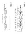
- FIG. 3shows a schematic functional block diagram of a polar transmitter architecture based on linear reconstruction of a phase and zero-order-hold envelope, in which the preferred embodiments can be implemented for generating or deriving amplitude and phase components.
- instantaneous frequency samples f i [n] obtained from a phase-to-frequency converter 60 based on input phase samples ⁇ [n]are applied in the same phase-locked loop (PLL) circuit used to synthesize a carried signal, while envelope samples r[n] are applied to an amplitude control device 70 , e.g., a power amplifier (PA), in a zero-order-hold fashion, i.e., the input is sampled and held for a specified sample period.
- PLLphase-locked loop
- envelope samples r[n]are applied to an amplitude control device 70 , e.g., a power amplifier (PA), in a zero-order-hold fashion, i.e., the input is sampled and held for a specified sample period.
- PApower amplifier
- phase samplesexperience a first-order-hold interpolation thanks to the integration in the PLL loop.
- the polar-modulated output signal of the amplitude control device 70is passed through a band pass filtering stage 80 before being transmitted.
- FIG. 4shows a schematic functional block diagram of a polar baseband generator according to a second preferred embodiment. Similar to the first and subsequent preferred embodiments, it can be used, for example, as a polar baseband generator for the polar transmitter of FIG. 3 .
- the block diagram of FIG. 4is a reduced version of the block diagram of FIG. 2 , to keep the description simple and put focus only on modified parts of the architecture. Of course, other blocks of FIG. 2 , which are not shown in FIG. 4 , may be provided as well. This also applies to the subsequent preferred embodiments.
- the arbitrary function generator block 30 of FIG. 2has been replaced by a phase-to-frequency converter block 280 which is provided only in the lower branch and which outputs a modified phase signal ( ⁇ [m+1] ⁇ [m]). Also, it has been assumed that the sampling frequency fs/M after the CORDIC block 20 is sufficiently high for the phase, so that no second interpolation stage is required in the lower branch. In case the sampling frequency at the output of the CORDIC block 20 is not high enough, the right-hand side of the signal generator in FIG. 4 can be replaced by the block diagram of FIG. 5 or FIG. 6 , to arrive at the third or fourth preferred embodiment, respectively.
- FIG. 5shows a schematic functional block diagram of a modified implementation after the CORDIC block 20 of the polar baseband generator, according to the third preferred embodiment.
- a phase-to-frequency converter block 290 of the lower branchis now provided after a preceding second interpolation stage 220 and low pass filtering stage 260 .
- a higher sampling frequency fs M′/Mcan be provided at the phase-to-frequency converter block 290 .
- FIG. 6shows a schematic functional block diagram of another modification after the CORDIC block 20 polar baseband generator, according to a fourth preferred embodiment.
- the phase-to-frequency converter block 280 of the lower branch of the third preferred embodimentwhich can be operated at the lower sampling frequency fs/M, is provided.
- the second interpolation stage 220 and the low pass filtering stage 260to thereby obtain the higher sampling frequency fs M′/M at the phase output.
- zero paddingin one domain results in an increased sampling rate in the other domain.
- a common form of zero paddingis to append a string of zero-valued samples to the end of some time-domain sequence. This approach can be used in the preferred embodiments to implement the interpolation.
- the signal interpolation which takes place before application of the CORDIC algorithmcan be embedded in an inverse fast fourier transformation (IFFT) block which block is typically present in OFDM or similar systems. Then, interpolation can be achieved by padding zeros and running the IFFT at higher frequencies. For example in the IEEE 802.11a/g, a 64-IFFT block running at 20 MHz is defined. An interpolated signal (by a factor 2) can be obtained using a 128-IFFT block and a clock frequency of 40 MHz. The 128 samples are obtained by padding 64 zeros to the original 64 samples. The extra zeros are allocated on high frequency subcarriers.
- IFFTinverse fast fourier transformation
- this zero padding approachcould be scaled to obtain any required interpolation factor, as long as the latency of the enlarged-size IFFT block does not pose a problem.
- the up-scaled IFFT blockshould process the samples as fast as the original-sized IFFT block.
- FIG. 7shows a schematic functional block diagram of an interpolation scheme which can be used in the preferred embodiments.
- the constellation symbols(plus some already padded zeros and pilot signals) arrive at a sampling frequency rate f D . Subsequently, they are converted in serial-to-parallel conversion block 410 from serial to parallel transmission state and are then zero-padded in a zero padding block 420 . After round-robin de-multiplexing in a corresponding de-multiplexer 430 , de-multiplexed groups of N*K symbols are fed in parallel to N*K-size IFFT blocks 440 , 442 , and 444 .
- the preferred embodimentcan be used in any polar transmitter architecture for many wireless standards including but not restricted to IEEE 802.11a/b/g, IEEE 802.16 and IEEE 802.15.
- a polar signal generator and method of deriving phase and amplitude components from in-phase (I) and quadrature-phase (Q) components of an input signalhave been described, wherein the I and Q components are generated at a first sampling frequency based the input signal, and are then up-sampled in accordance with a predetermined first interpolation factor, to generate up-sampled I and Q components at a second sampling frequency higher than the first sampling frequency.
- the up-sampled I and Q componentsare converted into the phase and amplitude components, wherein the converting step is operated at the second sampling frequency.
- the phase and amplitude componentscan be further up-sampled, optionally by different sampling frequencies, to a third and a fourth sampling frequency.
- the proposed solution according to the above preferred embodimentscircumvents the disadvantages encountered with I/Q generation and polar conversion at high sampling frequencies. Additionally, the amplitude and phase components can be processed at different sampling frequencies.
- the present inventionis not restricted to the above preferred embodiments, but can be applied to any polar modulation architecture which is based on a generation of separated amplitude and phase modulation signals from Cartesian I and Q components. Any other number of interpolation units or circuits can be provided, as desired or applicable in possible implementations. Hence, the preferred embodiments may vary within the scope of the attached claims.
Landscapes
- Digital Transmission Methods That Use Modulated Carrier Waves (AREA)
- Amplitude Modulation (AREA)
- Steering Control In Accordance With Driving Conditions (AREA)
- Details Of Television Scanning (AREA)
- Oscillators With Electromechanical Resonators (AREA)
- Transmitters (AREA)
Abstract
Description
Claims (14)
Applications Claiming Priority (4)
| Application Number | Priority Date | Filing Date | Title |
|---|---|---|---|
| EP06115266.6 | 2006-06-12 | ||
| EP06115266 | 2006-06-12 | ||
| EP06115266 | 2006-06-12 | ||
| PCT/IB2007/052127WO2007144806A2 (en) | 2006-06-12 | 2007-06-06 | Polar signal generator |
Publications (2)
| Publication Number | Publication Date |
|---|---|
| US20090206940A1 US20090206940A1 (en) | 2009-08-20 |
| US8872596B2true US8872596B2 (en) | 2014-10-28 |
Family
ID=38832186
Family Applications (1)
| Application Number | Title | Priority Date | Filing Date |
|---|---|---|---|
| US12/304,310Active2030-12-06US8872596B2 (en) | 2006-06-12 | 2007-06-06 | Polar signal generator |
Country Status (6)
| Country | Link |
|---|---|
| US (1) | US8872596B2 (en) |
| EP (1) | EP2038995B1 (en) |
| CN (1) | CN101467345A (en) |
| AT (1) | ATE500647T1 (en) |
| DE (1) | DE602007012880D1 (en) |
| WO (1) | WO2007144806A2 (en) |
Cited By (1)
| Publication number | Priority date | Publication date | Assignee | Title |
|---|---|---|---|---|
| US20150363362A1 (en)* | 2014-06-13 | 2015-12-17 | Intel IP Corporation | Method, apparatus and computer program for determining an interpolated complex valued sample |
Families Citing this family (5)
| Publication number | Priority date | Publication date | Assignee | Title |
|---|---|---|---|---|
| WO2008001269A2 (en)* | 2006-06-28 | 2008-01-03 | Nxp B.V. | Phase-to- frequency conversion for polar transmitters |
| US9100254B2 (en)* | 2008-03-28 | 2015-08-04 | Qualcomm Incorporated | Method and system for transmit upsampling via IFFT |
| US9157940B2 (en)* | 2011-02-09 | 2015-10-13 | Smart Energy Instruments, Inc. | Power measurement device |
| US10128795B2 (en)* | 2016-01-06 | 2018-11-13 | Apple Inc. | Polar loop modulation techniques for wireless communication |
| US10454747B1 (en)* | 2018-09-07 | 2019-10-22 | Innophase, Inc. | Systems and methods for up-sampling a polar amplitude sample stream in a polar modulator |
Citations (10)
| Publication number | Priority date | Publication date | Assignee | Title |
|---|---|---|---|---|
| WO2001024356A1 (en) | 1999-09-29 | 2001-04-05 | Tait Electronics Limited | Improvements relating to eer transmitters |
| US20020168019A1 (en)* | 2001-05-09 | 2002-11-14 | Erik Bengtsson | Apparatus and method to reduce size and complexity of reconstruction filters in a multi-protocol transmitter |
| WO2004017590A1 (en) | 2002-08-19 | 2004-02-26 | The Regents Of The University Of California | Fpga implementation of a digital qam modulator |
| US20040212445A1 (en) | 2003-04-22 | 2004-10-28 | Haglan David E. | Filter method and apparatus for polar modulation |
| US6834084B2 (en) | 2002-05-06 | 2004-12-21 | Rf Micro Devices Inc | Direct digital polar modulator |
| US20050018790A1 (en) | 2003-07-22 | 2005-01-27 | M/A-Com, Inc. | Electromagnetic wave transmitter, receiver and transceiver systems, methods and articles of manufacture |
| EP1536554A2 (en) | 2003-11-28 | 2005-06-01 | Samsung Electronics Co., Ltd. | Digital frequency converter |
| US20050271161A1 (en) | 2004-06-04 | 2005-12-08 | Texas Instruments Incorporated | Digital amplitude modulation |
| US20080101500A1 (en)* | 2006-10-27 | 2008-05-01 | Dmitry Voloshin | Multiplier-less data processing techniques and related implementations adapted for use in polar modulator |
| US20090323510A1 (en)* | 2004-01-06 | 2009-12-31 | Simeon Furrer | Modulation and demodulation of OFDM signals |
- 2007
- 2007-06-06USUS12/304,310patent/US8872596B2/enactiveActive
- 2007-06-06WOPCT/IB2007/052127patent/WO2007144806A2/enactiveApplication Filing
- 2007-06-06EPEP07766656Apatent/EP2038995B1/ennot_activeNot-in-force
- 2007-06-06DEDE602007012880Tpatent/DE602007012880D1/enactiveActive
- 2007-06-06CNCN200780021597.6Apatent/CN101467345A/enactivePending
- 2007-06-06ATAT07766656Tpatent/ATE500647T1/ennot_activeIP Right Cessation
Patent Citations (10)
| Publication number | Priority date | Publication date | Assignee | Title |
|---|---|---|---|---|
| WO2001024356A1 (en) | 1999-09-29 | 2001-04-05 | Tait Electronics Limited | Improvements relating to eer transmitters |
| US20020168019A1 (en)* | 2001-05-09 | 2002-11-14 | Erik Bengtsson | Apparatus and method to reduce size and complexity of reconstruction filters in a multi-protocol transmitter |
| US6834084B2 (en) | 2002-05-06 | 2004-12-21 | Rf Micro Devices Inc | Direct digital polar modulator |
| WO2004017590A1 (en) | 2002-08-19 | 2004-02-26 | The Regents Of The University Of California | Fpga implementation of a digital qam modulator |
| US20040212445A1 (en) | 2003-04-22 | 2004-10-28 | Haglan David E. | Filter method and apparatus for polar modulation |
| US20050018790A1 (en) | 2003-07-22 | 2005-01-27 | M/A-Com, Inc. | Electromagnetic wave transmitter, receiver and transceiver systems, methods and articles of manufacture |
| EP1536554A2 (en) | 2003-11-28 | 2005-06-01 | Samsung Electronics Co., Ltd. | Digital frequency converter |
| US20090323510A1 (en)* | 2004-01-06 | 2009-12-31 | Simeon Furrer | Modulation and demodulation of OFDM signals |
| US20050271161A1 (en) | 2004-06-04 | 2005-12-08 | Texas Instruments Incorporated | Digital amplitude modulation |
| US20080101500A1 (en)* | 2006-10-27 | 2008-05-01 | Dmitry Voloshin | Multiplier-less data processing techniques and related implementations adapted for use in polar modulator |
Cited By (2)
| Publication number | Priority date | Publication date | Assignee | Title |
|---|---|---|---|---|
| US20150363362A1 (en)* | 2014-06-13 | 2015-12-17 | Intel IP Corporation | Method, apparatus and computer program for determining an interpolated complex valued sample |
| US9871682B2 (en)* | 2014-06-13 | 2018-01-16 | Intel IP Corporation | Method, apparatus and computer program for determining an interpolated complex valued sample |
Also Published As
| Publication number | Publication date |
|---|---|
| CN101467345A (en) | 2009-06-24 |
| US20090206940A1 (en) | 2009-08-20 |
| EP2038995A2 (en) | 2009-03-25 |
| EP2038995B1 (en) | 2011-03-02 |
| WO2007144806A2 (en) | 2007-12-21 |
| WO2007144806A3 (en) | 2008-10-16 |
| ATE500647T1 (en) | 2011-03-15 |
| DE602007012880D1 (en) | 2011-04-14 |
Similar Documents
| Publication | Publication Date | Title |
|---|---|---|
| US8086189B2 (en) | Phase-to-frequency conversion for polar transmitters | |
| US7526261B2 (en) | RF power transmission, modulation, and amplification, including cartesian 4-branch embodiments | |
| JP5006403B2 (en) | Switch modulation of radio frequency amplifiers | |
| US8872596B2 (en) | Polar signal generator | |
| JP6983331B2 (en) | Radio frequency (RF) transmitter and RF transmission method | |
| CN102752246B (en) | Radiofrequency launcher, integrated device electronics, wireless communication unit and method | |
| US20100124290A1 (en) | Digital Signal Transmission for Wireless Communication | |
| CN105577199B (en) | Transmitter circuit, communication unit and method for amplifying composite orthogonal signal | |
| US7095277B2 (en) | Method and arrangement for a power amplifier | |
| EP1992135A2 (en) | Rf transmitter with interleaved iq modulation | |
| WO2003047101A1 (en) | Modulated radio frequency signal generation method and modulated signal source | |
| CN1310880A (en) | Method and apparatus for modulating digital data | |
| CN108702351A (en) | Signal Processing Architecture for Transmitter | |
| US20050185723A1 (en) | Peak suppression of multi-carrier signal with different modulation | |
| EP2186284B1 (en) | Signal modulation for switched mode power amplifiers technical field of the invention | |
| US20050111576A1 (en) | Peak-to-average reduction technique for multi-carrier power amplifiers | |
| AU2020274536B2 (en) | Programmable polar and cartesian radio frequency digital to analog converter | |
| JP2007507151A (en) | Apparatus and method for digitally realizing broadband multi-carrier | |
| US20050163038A1 (en) | Multi-carrier peak reduction using amplitude clipping and phase rotation | |
| JP2011527172A (en) | Digital modulator | |
| CN114499556B (en) | Multi-mode all-digital transmitter with continuous frequency conversion | |
| JP6177057B2 (en) | IC for wireless communication | |
| EP3499728A1 (en) | Digital power amplification circuit | |
| EP2043258A1 (en) | A method for signal amplification, a switched mode amplifier system, a base station and a communication network therefor | |
| WO2019103747A1 (en) | Apparatus and method for driving a digital-to-analog converter, and apparatuses and methods for generating a radio frequency signal |
Legal Events
| Date | Code | Title | Description |
|---|---|---|---|
| AS | Assignment | Owner name:NXP, B.V., NETHERLANDS Free format text:ASSIGNMENT OF ASSIGNORS INTEREST;ASSIGNORS:COLLADOS ASENSIO, MANEL;PAVLOVIC, NENAD;VIDOJKOVIC, VOJKAN;AND OTHERS;REEL/FRAME:021961/0807 Effective date:20081211 | |
| STCF | Information on status: patent grant | Free format text:PATENTED CASE | |
| AS | Assignment | Owner name:MORGAN STANLEY SENIOR FUNDING, INC., MARYLAND Free format text:SECURITY AGREEMENT SUPPLEMENT;ASSIGNOR:NXP B.V.;REEL/FRAME:038017/0058 Effective date:20160218 | |
| AS | Assignment | Owner name:MORGAN STANLEY SENIOR FUNDING, INC., MARYLAND Free format text:CORRECTIVE ASSIGNMENT TO CORRECT THE REMOVE APPLICATION 12092129 PREVIOUSLY RECORDED ON REEL 038017 FRAME 0058. ASSIGNOR(S) HEREBY CONFIRMS THE SECURITY AGREEMENT SUPPLEMENT;ASSIGNOR:NXP B.V.;REEL/FRAME:039361/0212 Effective date:20160218 | |
| AS | Assignment | Owner name:MORGAN STANLEY SENIOR FUNDING, INC., MARYLAND Free format text:CORRECTIVE ASSIGNMENT TO CORRECT THE REMOVE APPLICATION 12681366 PREVIOUSLY RECORDED ON REEL 039361 FRAME 0212. ASSIGNOR(S) HEREBY CONFIRMS THE SECURITY AGREEMENT SUPPLEMENT;ASSIGNOR:NXP B.V.;REEL/FRAME:042762/0145 Effective date:20160218 Owner name:MORGAN STANLEY SENIOR FUNDING, INC., MARYLAND Free format text:CORRECTIVE ASSIGNMENT TO CORRECT THE REMOVE APPLICATION 12681366 PREVIOUSLY RECORDED ON REEL 038017 FRAME 0058. ASSIGNOR(S) HEREBY CONFIRMS THE SECURITY AGREEMENT SUPPLEMENT;ASSIGNOR:NXP B.V.;REEL/FRAME:042985/0001 Effective date:20160218 | |
| MAFP | Maintenance fee payment | Free format text:PAYMENT OF MAINTENANCE FEE, 4TH YEAR, LARGE ENTITY (ORIGINAL EVENT CODE: M1551) Year of fee payment:4 | |
| AS | Assignment | Owner name:NXP B.V., NETHERLANDS Free format text:RELEASE BY SECURED PARTY;ASSIGNOR:MORGAN STANLEY SENIOR FUNDING, INC.;REEL/FRAME:050745/0001 Effective date:20190903 | |
| AS | Assignment | Owner name:MORGAN STANLEY SENIOR FUNDING, INC., MARYLAND Free format text:CORRECTIVE ASSIGNMENT TO CORRECT THE REMOVE APPLICATION 12298143 PREVIOUSLY RECORDED ON REEL 042762 FRAME 0145. ASSIGNOR(S) HEREBY CONFIRMS THE SECURITY AGREEMENT SUPPLEMENT;ASSIGNOR:NXP B.V.;REEL/FRAME:051145/0184 Effective date:20160218 Owner name:MORGAN STANLEY SENIOR FUNDING, INC., MARYLAND Free format text:CORRECTIVE ASSIGNMENT TO CORRECT THE REMOVE APPLICATION 12298143 PREVIOUSLY RECORDED ON REEL 039361 FRAME 0212. ASSIGNOR(S) HEREBY CONFIRMS THE SECURITY AGREEMENT SUPPLEMENT;ASSIGNOR:NXP B.V.;REEL/FRAME:051029/0387 Effective date:20160218 Owner name:MORGAN STANLEY SENIOR FUNDING, INC., MARYLAND Free format text:CORRECTIVE ASSIGNMENT TO CORRECT THE REMOVE APPLICATION 12298143 PREVIOUSLY RECORDED ON REEL 042985 FRAME 0001. ASSIGNOR(S) HEREBY CONFIRMS THE SECURITY AGREEMENT SUPPLEMENT;ASSIGNOR:NXP B.V.;REEL/FRAME:051029/0001 Effective date:20160218 Owner name:MORGAN STANLEY SENIOR FUNDING, INC., MARYLAND Free format text:CORRECTIVE ASSIGNMENT TO CORRECT THE REMOVE APPLICATION12298143 PREVIOUSLY RECORDED ON REEL 042985 FRAME 0001. ASSIGNOR(S) HEREBY CONFIRMS THE SECURITY AGREEMENT SUPPLEMENT;ASSIGNOR:NXP B.V.;REEL/FRAME:051029/0001 Effective date:20160218 Owner name:MORGAN STANLEY SENIOR FUNDING, INC., MARYLAND Free format text:CORRECTIVE ASSIGNMENT TO CORRECT THE REMOVE APPLICATION12298143 PREVIOUSLY RECORDED ON REEL 039361 FRAME 0212. ASSIGNOR(S) HEREBY CONFIRMS THE SECURITY AGREEMENT SUPPLEMENT;ASSIGNOR:NXP B.V.;REEL/FRAME:051029/0387 Effective date:20160218 Owner name:MORGAN STANLEY SENIOR FUNDING, INC., MARYLAND Free format text:CORRECTIVE ASSIGNMENT TO CORRECT THE REMOVE APPLICATION 12298143 PREVIOUSLY RECORDED ON REEL 038017 FRAME 0058. ASSIGNOR(S) HEREBY CONFIRMS THE SECURITY AGREEMENT SUPPLEMENT;ASSIGNOR:NXP B.V.;REEL/FRAME:051030/0001 Effective date:20160218 Owner name:MORGAN STANLEY SENIOR FUNDING, INC., MARYLAND Free format text:CORRECTIVE ASSIGNMENT TO CORRECT THE REMOVE APPLICATION12298143 PREVIOUSLY RECORDED ON REEL 042762 FRAME 0145. ASSIGNOR(S) HEREBY CONFIRMS THE SECURITY AGREEMENT SUPPLEMENT;ASSIGNOR:NXP B.V.;REEL/FRAME:051145/0184 Effective date:20160218 | |
| MAFP | Maintenance fee payment | Free format text:PAYMENT OF MAINTENANCE FEE, 8TH YEAR, LARGE ENTITY (ORIGINAL EVENT CODE: M1552); ENTITY STATUS OF PATENT OWNER: LARGE ENTITY Year of fee payment:8 |