US8872318B2 - Through interposer wire bond using low CTE interposer with coarse slot apertures - Google Patents
Through interposer wire bond using low CTE interposer with coarse slot aperturesDownload PDFInfo
- Publication number
- US8872318B2 US8872318B2US13/216,465US201113216465AUS8872318B2US 8872318 B2US8872318 B2US 8872318B2US 201113216465 AUS201113216465 AUS 201113216465AUS 8872318 B2US8872318 B2US 8872318B2
- Authority
- US
- United States
- Prior art keywords
- microelectronic
- substrate
- contacts
- microelectronic element
- package
- Prior art date
- Legal status (The legal status is an assumption and is not a legal conclusion. Google has not performed a legal analysis and makes no representation as to the accuracy of the status listed.)
- Active, expires
Links
Images


Classifications
- H—ELECTRICITY
- H01—ELECTRIC ELEMENTS
- H01L—SEMICONDUCTOR DEVICES NOT COVERED BY CLASS H10
- H01L24/00—Arrangements for connecting or disconnecting semiconductor or solid-state bodies; Methods or apparatus related thereto
- H01L24/73—Means for bonding being of different types provided for in two or more of groups H01L24/10, H01L24/18, H01L24/26, H01L24/34, H01L24/42, H01L24/50, H01L24/63, H01L24/71
- H—ELECTRICITY
- H01—ELECTRIC ELEMENTS
- H01L—SEMICONDUCTOR DEVICES NOT COVERED BY CLASS H10
- H01L21/00—Processes or apparatus adapted for the manufacture or treatment of semiconductor or solid state devices or of parts thereof
- H01L21/02—Manufacture or treatment of semiconductor devices or of parts thereof
- H01L21/04—Manufacture or treatment of semiconductor devices or of parts thereof the devices having potential barriers, e.g. a PN junction, depletion layer or carrier concentration layer
- H01L21/48—Manufacture or treatment of parts, e.g. containers, prior to assembly of the devices, using processes not provided for in a single one of the groups H01L21/18 - H01L21/326 or H10D48/04 - H10D48/07
- H01L21/4814—Conductive parts
- H01L21/4846—Leads on or in insulating or insulated substrates, e.g. metallisation
- H01L21/486—Via connections through the substrate with or without pins
- H—ELECTRICITY
- H01—ELECTRIC ELEMENTS
- H01L—SEMICONDUCTOR DEVICES NOT COVERED BY CLASS H10
- H01L23/00—Details of semiconductor or other solid state devices
- H01L23/12—Mountings, e.g. non-detachable insulating substrates
- H01L23/13—Mountings, e.g. non-detachable insulating substrates characterised by the shape
- H—ELECTRICITY
- H01—ELECTRIC ELEMENTS
- H01L—SEMICONDUCTOR DEVICES NOT COVERED BY CLASS H10
- H01L23/00—Details of semiconductor or other solid state devices
- H01L23/48—Arrangements for conducting electric current to or from the solid state body in operation, e.g. leads, terminal arrangements ; Selection of materials therefor
- H01L23/488—Arrangements for conducting electric current to or from the solid state body in operation, e.g. leads, terminal arrangements ; Selection of materials therefor consisting of soldered or bonded constructions
- H01L23/498—Leads, i.e. metallisations or lead-frames on insulating substrates, e.g. chip carriers
- H01L23/49811—Additional leads joined to the metallisation on the insulating substrate, e.g. pins, bumps, wires, flat leads
- H—ELECTRICITY
- H01—ELECTRIC ELEMENTS
- H01L—SEMICONDUCTOR DEVICES NOT COVERED BY CLASS H10
- H01L23/00—Details of semiconductor or other solid state devices
- H01L23/48—Arrangements for conducting electric current to or from the solid state body in operation, e.g. leads, terminal arrangements ; Selection of materials therefor
- H01L23/488—Arrangements for conducting electric current to or from the solid state body in operation, e.g. leads, terminal arrangements ; Selection of materials therefor consisting of soldered or bonded constructions
- H01L23/498—Leads, i.e. metallisations or lead-frames on insulating substrates, e.g. chip carriers
- H01L23/49827—Via connections through the substrates, e.g. pins going through the substrate, coaxial cables
- H—ELECTRICITY
- H01—ELECTRIC ELEMENTS
- H01L—SEMICONDUCTOR DEVICES NOT COVERED BY CLASS H10
- H01L24/00—Arrangements for connecting or disconnecting semiconductor or solid-state bodies; Methods or apparatus related thereto
- H01L24/93—Batch processes
- H01L24/95—Batch processes at chip-level, i.e. with connecting carried out on a plurality of singulated devices, i.e. on diced chips
- H01L24/97—Batch processes at chip-level, i.e. with connecting carried out on a plurality of singulated devices, i.e. on diced chips the devices being connected to a common substrate, e.g. interposer, said common substrate being separable into individual assemblies after connecting
- H—ELECTRICITY
- H01—ELECTRIC ELEMENTS
- H01L—SEMICONDUCTOR DEVICES NOT COVERED BY CLASS H10
- H01L25/00—Assemblies consisting of a plurality of semiconductor or other solid state devices
- H01L25/03—Assemblies consisting of a plurality of semiconductor or other solid state devices all the devices being of a type provided for in a single subclass of subclasses H10B, H10D, H10F, H10H, H10K or H10N, e.g. assemblies of rectifier diodes
- H01L25/04—Assemblies consisting of a plurality of semiconductor or other solid state devices all the devices being of a type provided for in a single subclass of subclasses H10B, H10D, H10F, H10H, H10K or H10N, e.g. assemblies of rectifier diodes the devices not having separate containers
- H01L25/065—Assemblies consisting of a plurality of semiconductor or other solid state devices all the devices being of a type provided for in a single subclass of subclasses H10B, H10D, H10F, H10H, H10K or H10N, e.g. assemblies of rectifier diodes the devices not having separate containers the devices being of a type provided for in group H10D89/00
- H01L25/0657—Stacked arrangements of devices
- H—ELECTRICITY
- H01—ELECTRIC ELEMENTS
- H01L—SEMICONDUCTOR DEVICES NOT COVERED BY CLASS H10
- H01L2224/00—Indexing scheme for arrangements for connecting or disconnecting semiconductor or solid-state bodies and methods related thereto as covered by H01L24/00
- H01L2224/01—Means for bonding being attached to, or being formed on, the surface to be connected, e.g. chip-to-package, die-attach, "first-level" interconnects; Manufacturing methods related thereto
- H01L2224/10—Bump connectors; Manufacturing methods related thereto
- H01L2224/12—Structure, shape, material or disposition of the bump connectors prior to the connecting process
- H01L2224/13—Structure, shape, material or disposition of the bump connectors prior to the connecting process of an individual bump connector
- H01L2224/13001—Core members of the bump connector
- H01L2224/13099—Material
- H01L2224/131—Material with a principal constituent of the material being a metal or a metalloid, e.g. boron [B], silicon [Si], germanium [Ge], arsenic [As], antimony [Sb], tellurium [Te] and polonium [Po], and alloys thereof
- H01L2224/13101—Material with a principal constituent of the material being a metal or a metalloid, e.g. boron [B], silicon [Si], germanium [Ge], arsenic [As], antimony [Sb], tellurium [Te] and polonium [Po], and alloys thereof the principal constituent melting at a temperature of less than 400°C
- H01L2224/13109—Indium [In] as principal constituent
- H—ELECTRICITY
- H01—ELECTRIC ELEMENTS
- H01L—SEMICONDUCTOR DEVICES NOT COVERED BY CLASS H10
- H01L2224/00—Indexing scheme for arrangements for connecting or disconnecting semiconductor or solid-state bodies and methods related thereto as covered by H01L24/00
- H01L2224/01—Means for bonding being attached to, or being formed on, the surface to be connected, e.g. chip-to-package, die-attach, "first-level" interconnects; Manufacturing methods related thereto
- H01L2224/10—Bump connectors; Manufacturing methods related thereto
- H01L2224/12—Structure, shape, material or disposition of the bump connectors prior to the connecting process
- H01L2224/13—Structure, shape, material or disposition of the bump connectors prior to the connecting process of an individual bump connector
- H01L2224/13001—Core members of the bump connector
- H01L2224/13099—Material
- H01L2224/131—Material with a principal constituent of the material being a metal or a metalloid, e.g. boron [B], silicon [Si], germanium [Ge], arsenic [As], antimony [Sb], tellurium [Te] and polonium [Po], and alloys thereof
- H01L2224/13101—Material with a principal constituent of the material being a metal or a metalloid, e.g. boron [B], silicon [Si], germanium [Ge], arsenic [As], antimony [Sb], tellurium [Te] and polonium [Po], and alloys thereof the principal constituent melting at a temperature of less than 400°C
- H01L2224/13111—Tin [Sn] as principal constituent
- H—ELECTRICITY
- H01—ELECTRIC ELEMENTS
- H01L—SEMICONDUCTOR DEVICES NOT COVERED BY CLASS H10
- H01L2224/00—Indexing scheme for arrangements for connecting or disconnecting semiconductor or solid-state bodies and methods related thereto as covered by H01L24/00
- H01L2224/01—Means for bonding being attached to, or being formed on, the surface to be connected, e.g. chip-to-package, die-attach, "first-level" interconnects; Manufacturing methods related thereto
- H01L2224/10—Bump connectors; Manufacturing methods related thereto
- H01L2224/12—Structure, shape, material or disposition of the bump connectors prior to the connecting process
- H01L2224/13—Structure, shape, material or disposition of the bump connectors prior to the connecting process of an individual bump connector
- H01L2224/13001—Core members of the bump connector
- H01L2224/13099—Material
- H01L2224/131—Material with a principal constituent of the material being a metal or a metalloid, e.g. boron [B], silicon [Si], germanium [Ge], arsenic [As], antimony [Sb], tellurium [Te] and polonium [Po], and alloys thereof
- H01L2224/13138—Material with a principal constituent of the material being a metal or a metalloid, e.g. boron [B], silicon [Si], germanium [Ge], arsenic [As], antimony [Sb], tellurium [Te] and polonium [Po], and alloys thereof the principal constituent melting at a temperature of greater than or equal to 950°C and less than 1550°C
- H01L2224/13144—Gold [Au] as principal constituent
- H—ELECTRICITY
- H01—ELECTRIC ELEMENTS
- H01L—SEMICONDUCTOR DEVICES NOT COVERED BY CLASS H10
- H01L2224/00—Indexing scheme for arrangements for connecting or disconnecting semiconductor or solid-state bodies and methods related thereto as covered by H01L24/00
- H01L2224/01—Means for bonding being attached to, or being formed on, the surface to be connected, e.g. chip-to-package, die-attach, "first-level" interconnects; Manufacturing methods related thereto
- H01L2224/10—Bump connectors; Manufacturing methods related thereto
- H01L2224/12—Structure, shape, material or disposition of the bump connectors prior to the connecting process
- H01L2224/13—Structure, shape, material or disposition of the bump connectors prior to the connecting process of an individual bump connector
- H01L2224/13001—Core members of the bump connector
- H01L2224/13099—Material
- H01L2224/131—Material with a principal constituent of the material being a metal or a metalloid, e.g. boron [B], silicon [Si], germanium [Ge], arsenic [As], antimony [Sb], tellurium [Te] and polonium [Po], and alloys thereof
- H01L2224/13138—Material with a principal constituent of the material being a metal or a metalloid, e.g. boron [B], silicon [Si], germanium [Ge], arsenic [As], antimony [Sb], tellurium [Te] and polonium [Po], and alloys thereof the principal constituent melting at a temperature of greater than or equal to 950°C and less than 1550°C
- H01L2224/13147—Copper [Cu] as principal constituent
- H—ELECTRICITY
- H01—ELECTRIC ELEMENTS
- H01L—SEMICONDUCTOR DEVICES NOT COVERED BY CLASS H10
- H01L2224/00—Indexing scheme for arrangements for connecting or disconnecting semiconductor or solid-state bodies and methods related thereto as covered by H01L24/00
- H01L2224/01—Means for bonding being attached to, or being formed on, the surface to be connected, e.g. chip-to-package, die-attach, "first-level" interconnects; Manufacturing methods related thereto
- H01L2224/10—Bump connectors; Manufacturing methods related thereto
- H01L2224/15—Structure, shape, material or disposition of the bump connectors after the connecting process
- H01L2224/16—Structure, shape, material or disposition of the bump connectors after the connecting process of an individual bump connector
- H01L2224/161—Disposition
- H01L2224/16135—Disposition the bump connector connecting between different semiconductor or solid-state bodies, i.e. chip-to-chip
- H01L2224/16145—Disposition the bump connector connecting between different semiconductor or solid-state bodies, i.e. chip-to-chip the bodies being stacked
- H—ELECTRICITY
- H01—ELECTRIC ELEMENTS
- H01L—SEMICONDUCTOR DEVICES NOT COVERED BY CLASS H10
- H01L2224/00—Indexing scheme for arrangements for connecting or disconnecting semiconductor or solid-state bodies and methods related thereto as covered by H01L24/00
- H01L2224/01—Means for bonding being attached to, or being formed on, the surface to be connected, e.g. chip-to-package, die-attach, "first-level" interconnects; Manufacturing methods related thereto
- H01L2224/10—Bump connectors; Manufacturing methods related thereto
- H01L2224/15—Structure, shape, material or disposition of the bump connectors after the connecting process
- H01L2224/16—Structure, shape, material or disposition of the bump connectors after the connecting process of an individual bump connector
- H01L2224/161—Disposition
- H01L2224/16151—Disposition the bump connector connecting between a semiconductor or solid-state body and an item not being a semiconductor or solid-state body, e.g. chip-to-substrate, chip-to-passive
- H01L2224/16221—Disposition the bump connector connecting between a semiconductor or solid-state body and an item not being a semiconductor or solid-state body, e.g. chip-to-substrate, chip-to-passive the body and the item being stacked
- H01L2224/16225—Disposition the bump connector connecting between a semiconductor or solid-state body and an item not being a semiconductor or solid-state body, e.g. chip-to-substrate, chip-to-passive the body and the item being stacked the item being non-metallic, e.g. insulating substrate with or without metallisation
- H01L2224/16227—Disposition the bump connector connecting between a semiconductor or solid-state body and an item not being a semiconductor or solid-state body, e.g. chip-to-substrate, chip-to-passive the body and the item being stacked the item being non-metallic, e.g. insulating substrate with or without metallisation the bump connector connecting to a bond pad of the item
- H—ELECTRICITY
- H01—ELECTRIC ELEMENTS
- H01L—SEMICONDUCTOR DEVICES NOT COVERED BY CLASS H10
- H01L2224/00—Indexing scheme for arrangements for connecting or disconnecting semiconductor or solid-state bodies and methods related thereto as covered by H01L24/00
- H01L2224/01—Means for bonding being attached to, or being formed on, the surface to be connected, e.g. chip-to-package, die-attach, "first-level" interconnects; Manufacturing methods related thereto
- H01L2224/26—Layer connectors, e.g. plate connectors, solder or adhesive layers; Manufacturing methods related thereto
- H01L2224/31—Structure, shape, material or disposition of the layer connectors after the connecting process
- H01L2224/32—Structure, shape, material or disposition of the layer connectors after the connecting process of an individual layer connector
- H01L2224/321—Disposition
- H01L2224/32135—Disposition the layer connector connecting between different semiconductor or solid-state bodies, i.e. chip-to-chip
- H01L2224/32145—Disposition the layer connector connecting between different semiconductor or solid-state bodies, i.e. chip-to-chip the bodies being stacked
- H—ELECTRICITY
- H01—ELECTRIC ELEMENTS
- H01L—SEMICONDUCTOR DEVICES NOT COVERED BY CLASS H10
- H01L2224/00—Indexing scheme for arrangements for connecting or disconnecting semiconductor or solid-state bodies and methods related thereto as covered by H01L24/00
- H01L2224/01—Means for bonding being attached to, or being formed on, the surface to be connected, e.g. chip-to-package, die-attach, "first-level" interconnects; Manufacturing methods related thereto
- H01L2224/26—Layer connectors, e.g. plate connectors, solder or adhesive layers; Manufacturing methods related thereto
- H01L2224/31—Structure, shape, material or disposition of the layer connectors after the connecting process
- H01L2224/32—Structure, shape, material or disposition of the layer connectors after the connecting process of an individual layer connector
- H01L2224/321—Disposition
- H01L2224/32151—Disposition the layer connector connecting between a semiconductor or solid-state body and an item not being a semiconductor or solid-state body, e.g. chip-to-substrate, chip-to-passive
- H01L2224/32221—Disposition the layer connector connecting between a semiconductor or solid-state body and an item not being a semiconductor or solid-state body, e.g. chip-to-substrate, chip-to-passive the body and the item being stacked
- H01L2224/32225—Disposition the layer connector connecting between a semiconductor or solid-state body and an item not being a semiconductor or solid-state body, e.g. chip-to-substrate, chip-to-passive the body and the item being stacked the item being non-metallic, e.g. insulating substrate with or without metallisation
- H—ELECTRICITY
- H01—ELECTRIC ELEMENTS
- H01L—SEMICONDUCTOR DEVICES NOT COVERED BY CLASS H10
- H01L2224/00—Indexing scheme for arrangements for connecting or disconnecting semiconductor or solid-state bodies and methods related thereto as covered by H01L24/00
- H01L2224/01—Means for bonding being attached to, or being formed on, the surface to be connected, e.g. chip-to-package, die-attach, "first-level" interconnects; Manufacturing methods related thereto
- H01L2224/42—Wire connectors; Manufacturing methods related thereto
- H01L2224/47—Structure, shape, material or disposition of the wire connectors after the connecting process
- H01L2224/48—Structure, shape, material or disposition of the wire connectors after the connecting process of an individual wire connector
- H01L2224/481—Disposition
- H01L2224/48151—Connecting between a semiconductor or solid-state body and an item not being a semiconductor or solid-state body, e.g. chip-to-substrate, chip-to-passive
- H01L2224/48221—Connecting between a semiconductor or solid-state body and an item not being a semiconductor or solid-state body, e.g. chip-to-substrate, chip-to-passive the body and the item being stacked
- H01L2224/48225—Connecting between a semiconductor or solid-state body and an item not being a semiconductor or solid-state body, e.g. chip-to-substrate, chip-to-passive the body and the item being stacked the item being non-metallic, e.g. insulating substrate with or without metallisation
- H01L2224/48227—Connecting between a semiconductor or solid-state body and an item not being a semiconductor or solid-state body, e.g. chip-to-substrate, chip-to-passive the body and the item being stacked the item being non-metallic, e.g. insulating substrate with or without metallisation connecting the wire to a bond pad of the item
- H—ELECTRICITY
- H01—ELECTRIC ELEMENTS
- H01L—SEMICONDUCTOR DEVICES NOT COVERED BY CLASS H10
- H01L2224/00—Indexing scheme for arrangements for connecting or disconnecting semiconductor or solid-state bodies and methods related thereto as covered by H01L24/00
- H01L2224/01—Means for bonding being attached to, or being formed on, the surface to be connected, e.g. chip-to-package, die-attach, "first-level" interconnects; Manufacturing methods related thereto
- H01L2224/42—Wire connectors; Manufacturing methods related thereto
- H01L2224/47—Structure, shape, material or disposition of the wire connectors after the connecting process
- H01L2224/48—Structure, shape, material or disposition of the wire connectors after the connecting process of an individual wire connector
- H01L2224/481—Disposition
- H01L2224/48151—Connecting between a semiconductor or solid-state body and an item not being a semiconductor or solid-state body, e.g. chip-to-substrate, chip-to-passive
- H01L2224/48221—Connecting between a semiconductor or solid-state body and an item not being a semiconductor or solid-state body, e.g. chip-to-substrate, chip-to-passive the body and the item being stacked
- H01L2224/48225—Connecting between a semiconductor or solid-state body and an item not being a semiconductor or solid-state body, e.g. chip-to-substrate, chip-to-passive the body and the item being stacked the item being non-metallic, e.g. insulating substrate with or without metallisation
- H01L2224/4824—Connecting between the body and an opposite side of the item with respect to the body
- H—ELECTRICITY
- H01—ELECTRIC ELEMENTS
- H01L—SEMICONDUCTOR DEVICES NOT COVERED BY CLASS H10
- H01L2224/00—Indexing scheme for arrangements for connecting or disconnecting semiconductor or solid-state bodies and methods related thereto as covered by H01L24/00
- H01L2224/73—Means for bonding being of different types provided for in two or more of groups H01L2224/10, H01L2224/18, H01L2224/26, H01L2224/34, H01L2224/42, H01L2224/50, H01L2224/63, H01L2224/71
- H01L2224/732—Location after the connecting process
- H01L2224/73201—Location after the connecting process on the same surface
- H01L2224/73203—Bump and layer connectors
- H01L2224/73204—Bump and layer connectors the bump connector being embedded into the layer connector
- H—ELECTRICITY
- H01—ELECTRIC ELEMENTS
- H01L—SEMICONDUCTOR DEVICES NOT COVERED BY CLASS H10
- H01L2224/00—Indexing scheme for arrangements for connecting or disconnecting semiconductor or solid-state bodies and methods related thereto as covered by H01L24/00
- H01L2224/73—Means for bonding being of different types provided for in two or more of groups H01L2224/10, H01L2224/18, H01L2224/26, H01L2224/34, H01L2224/42, H01L2224/50, H01L2224/63, H01L2224/71
- H01L2224/732—Location after the connecting process
- H01L2224/73201—Location after the connecting process on the same surface
- H01L2224/73215—Layer and wire connectors
- H—ELECTRICITY
- H01—ELECTRIC ELEMENTS
- H01L—SEMICONDUCTOR DEVICES NOT COVERED BY CLASS H10
- H01L2224/00—Indexing scheme for arrangements for connecting or disconnecting semiconductor or solid-state bodies and methods related thereto as covered by H01L24/00
- H01L2224/73—Means for bonding being of different types provided for in two or more of groups H01L2224/10, H01L2224/18, H01L2224/26, H01L2224/34, H01L2224/42, H01L2224/50, H01L2224/63, H01L2224/71
- H01L2224/732—Location after the connecting process
- H01L2224/73251—Location after the connecting process on different surfaces
- H01L2224/73253—Bump and layer connectors
- H—ELECTRICITY
- H01—ELECTRIC ELEMENTS
- H01L—SEMICONDUCTOR DEVICES NOT COVERED BY CLASS H10
- H01L2224/00—Indexing scheme for arrangements for connecting or disconnecting semiconductor or solid-state bodies and methods related thereto as covered by H01L24/00
- H01L2224/73—Means for bonding being of different types provided for in two or more of groups H01L2224/10, H01L2224/18, H01L2224/26, H01L2224/34, H01L2224/42, H01L2224/50, H01L2224/63, H01L2224/71
- H01L2224/732—Location after the connecting process
- H01L2224/73251—Location after the connecting process on different surfaces
- H01L2224/73265—Layer and wire connectors
- H—ELECTRICITY
- H01—ELECTRIC ELEMENTS
- H01L—SEMICONDUCTOR DEVICES NOT COVERED BY CLASS H10
- H01L2224/00—Indexing scheme for arrangements for connecting or disconnecting semiconductor or solid-state bodies and methods related thereto as covered by H01L24/00
- H01L2224/80—Methods for connecting semiconductor or other solid state bodies using means for bonding being attached to, or being formed on, the surface to be connected
- H01L2224/81—Methods for connecting semiconductor or other solid state bodies using means for bonding being attached to, or being formed on, the surface to be connected using a bump connector
- H—ELECTRICITY
- H01—ELECTRIC ELEMENTS
- H01L—SEMICONDUCTOR DEVICES NOT COVERED BY CLASS H10
- H01L2224/00—Indexing scheme for arrangements for connecting or disconnecting semiconductor or solid-state bodies and methods related thereto as covered by H01L24/00
- H01L2224/80—Methods for connecting semiconductor or other solid state bodies using means for bonding being attached to, or being formed on, the surface to be connected
- H01L2224/83—Methods for connecting semiconductor or other solid state bodies using means for bonding being attached to, or being formed on, the surface to be connected using a layer connector
- H—ELECTRICITY
- H01—ELECTRIC ELEMENTS
- H01L—SEMICONDUCTOR DEVICES NOT COVERED BY CLASS H10
- H01L2224/00—Indexing scheme for arrangements for connecting or disconnecting semiconductor or solid-state bodies and methods related thereto as covered by H01L24/00
- H01L2224/80—Methods for connecting semiconductor or other solid state bodies using means for bonding being attached to, or being formed on, the surface to be connected
- H01L2224/85—Methods for connecting semiconductor or other solid state bodies using means for bonding being attached to, or being formed on, the surface to be connected using a wire connector
- H—ELECTRICITY
- H01—ELECTRIC ELEMENTS
- H01L—SEMICONDUCTOR DEVICES NOT COVERED BY CLASS H10
- H01L2224/00—Indexing scheme for arrangements for connecting or disconnecting semiconductor or solid-state bodies and methods related thereto as covered by H01L24/00
- H01L2224/93—Batch processes
- H01L2224/95—Batch processes at chip-level, i.e. with connecting carried out on a plurality of singulated devices, i.e. on diced chips
- H01L2224/97—Batch processes at chip-level, i.e. with connecting carried out on a plurality of singulated devices, i.e. on diced chips the devices being connected to a common substrate, e.g. interposer, said common substrate being separable into individual assemblies after connecting
- H—ELECTRICITY
- H01—ELECTRIC ELEMENTS
- H01L—SEMICONDUCTOR DEVICES NOT COVERED BY CLASS H10
- H01L2225/00—Details relating to assemblies covered by the group H01L25/00 but not provided for in its subgroups
- H01L2225/03—All the devices being of a type provided for in the same main group of the same subclass of class H10, e.g. assemblies of rectifier diodes
- H01L2225/04—All the devices being of a type provided for in the same main group of the same subclass of class H10, e.g. assemblies of rectifier diodes the devices not having separate containers
- H01L2225/065—All the devices being of a type provided for in the same main group of the same subclass of class H10
- H01L2225/06503—Stacked arrangements of devices
- H01L2225/0651—Wire or wire-like electrical connections from device to substrate
- H—ELECTRICITY
- H01—ELECTRIC ELEMENTS
- H01L—SEMICONDUCTOR DEVICES NOT COVERED BY CLASS H10
- H01L2225/00—Details relating to assemblies covered by the group H01L25/00 but not provided for in its subgroups
- H01L2225/03—All the devices being of a type provided for in the same main group of the same subclass of class H10, e.g. assemblies of rectifier diodes
- H01L2225/04—All the devices being of a type provided for in the same main group of the same subclass of class H10, e.g. assemblies of rectifier diodes the devices not having separate containers
- H01L2225/065—All the devices being of a type provided for in the same main group of the same subclass of class H10
- H01L2225/06503—Stacked arrangements of devices
- H01L2225/06513—Bump or bump-like direct electrical connections between devices, e.g. flip-chip connection, solder bumps
- H—ELECTRICITY
- H01—ELECTRIC ELEMENTS
- H01L—SEMICONDUCTOR DEVICES NOT COVERED BY CLASS H10
- H01L2225/00—Details relating to assemblies covered by the group H01L25/00 but not provided for in its subgroups
- H01L2225/03—All the devices being of a type provided for in the same main group of the same subclass of class H10, e.g. assemblies of rectifier diodes
- H01L2225/04—All the devices being of a type provided for in the same main group of the same subclass of class H10, e.g. assemblies of rectifier diodes the devices not having separate containers
- H01L2225/065—All the devices being of a type provided for in the same main group of the same subclass of class H10
- H01L2225/06503—Stacked arrangements of devices
- H01L2225/06517—Bump or bump-like direct electrical connections from device to substrate
- H—ELECTRICITY
- H01—ELECTRIC ELEMENTS
- H01L—SEMICONDUCTOR DEVICES NOT COVERED BY CLASS H10
- H01L2225/00—Details relating to assemblies covered by the group H01L25/00 but not provided for in its subgroups
- H01L2225/03—All the devices being of a type provided for in the same main group of the same subclass of class H10, e.g. assemblies of rectifier diodes
- H01L2225/04—All the devices being of a type provided for in the same main group of the same subclass of class H10, e.g. assemblies of rectifier diodes the devices not having separate containers
- H01L2225/065—All the devices being of a type provided for in the same main group of the same subclass of class H10
- H01L2225/06503—Stacked arrangements of devices
- H01L2225/06541—Conductive via connections through the device, e.g. vertical interconnects, through silicon via [TSV]
- H—ELECTRICITY
- H01—ELECTRIC ELEMENTS
- H01L—SEMICONDUCTOR DEVICES NOT COVERED BY CLASS H10
- H01L2225/00—Details relating to assemblies covered by the group H01L25/00 but not provided for in its subgroups
- H01L2225/03—All the devices being of a type provided for in the same main group of the same subclass of class H10, e.g. assemblies of rectifier diodes
- H01L2225/04—All the devices being of a type provided for in the same main group of the same subclass of class H10, e.g. assemblies of rectifier diodes the devices not having separate containers
- H01L2225/065—All the devices being of a type provided for in the same main group of the same subclass of class H10
- H01L2225/06503—Stacked arrangements of devices
- H01L2225/06555—Geometry of the stack, e.g. form of the devices, geometry to facilitate stacking
- H01L2225/06558—Geometry of the stack, e.g. form of the devices, geometry to facilitate stacking the devices having passive surfaces facing each other, i.e. in a back-to-back arrangement
- H—ELECTRICITY
- H01—ELECTRIC ELEMENTS
- H01L—SEMICONDUCTOR DEVICES NOT COVERED BY CLASS H10
- H01L2225/00—Details relating to assemblies covered by the group H01L25/00 but not provided for in its subgroups
- H01L2225/03—All the devices being of a type provided for in the same main group of the same subclass of class H10, e.g. assemblies of rectifier diodes
- H01L2225/04—All the devices being of a type provided for in the same main group of the same subclass of class H10, e.g. assemblies of rectifier diodes the devices not having separate containers
- H01L2225/065—All the devices being of a type provided for in the same main group of the same subclass of class H10
- H01L2225/06503—Stacked arrangements of devices
- H01L2225/06555—Geometry of the stack, e.g. form of the devices, geometry to facilitate stacking
- H01L2225/06562—Geometry of the stack, e.g. form of the devices, geometry to facilitate stacking at least one device in the stack being rotated or offset
- H—ELECTRICITY
- H01—ELECTRIC ELEMENTS
- H01L—SEMICONDUCTOR DEVICES NOT COVERED BY CLASS H10
- H01L2225/00—Details relating to assemblies covered by the group H01L25/00 but not provided for in its subgroups
- H01L2225/03—All the devices being of a type provided for in the same main group of the same subclass of class H10, e.g. assemblies of rectifier diodes
- H01L2225/04—All the devices being of a type provided for in the same main group of the same subclass of class H10, e.g. assemblies of rectifier diodes the devices not having separate containers
- H01L2225/065—All the devices being of a type provided for in the same main group of the same subclass of class H10
- H01L2225/06503—Stacked arrangements of devices
- H01L2225/06555—Geometry of the stack, e.g. form of the devices, geometry to facilitate stacking
- H01L2225/06565—Geometry of the stack, e.g. form of the devices, geometry to facilitate stacking the devices having the same size and there being no auxiliary carrier between the devices
- H—ELECTRICITY
- H01—ELECTRIC ELEMENTS
- H01L—SEMICONDUCTOR DEVICES NOT COVERED BY CLASS H10
- H01L24/00—Arrangements for connecting or disconnecting semiconductor or solid-state bodies; Methods or apparatus related thereto
- H01L24/01—Means for bonding being attached to, or being formed on, the surface to be connected, e.g. chip-to-package, die-attach, "first-level" interconnects; Manufacturing methods related thereto
- H01L24/10—Bump connectors ; Manufacturing methods related thereto
- H01L24/15—Structure, shape, material or disposition of the bump connectors after the connecting process
- H01L24/16—Structure, shape, material or disposition of the bump connectors after the connecting process of an individual bump connector
- H—ELECTRICITY
- H01—ELECTRIC ELEMENTS
- H01L—SEMICONDUCTOR DEVICES NOT COVERED BY CLASS H10
- H01L24/00—Arrangements for connecting or disconnecting semiconductor or solid-state bodies; Methods or apparatus related thereto
- H01L24/01—Means for bonding being attached to, or being formed on, the surface to be connected, e.g. chip-to-package, die-attach, "first-level" interconnects; Manufacturing methods related thereto
- H01L24/26—Layer connectors, e.g. plate connectors, solder or adhesive layers; Manufacturing methods related thereto
- H01L24/31—Structure, shape, material or disposition of the layer connectors after the connecting process
- H01L24/32—Structure, shape, material or disposition of the layer connectors after the connecting process of an individual layer connector
- H—ELECTRICITY
- H01—ELECTRIC ELEMENTS
- H01L—SEMICONDUCTOR DEVICES NOT COVERED BY CLASS H10
- H01L24/00—Arrangements for connecting or disconnecting semiconductor or solid-state bodies; Methods or apparatus related thereto
- H01L24/01—Means for bonding being attached to, or being formed on, the surface to be connected, e.g. chip-to-package, die-attach, "first-level" interconnects; Manufacturing methods related thereto
- H01L24/42—Wire connectors; Manufacturing methods related thereto
- H01L24/47—Structure, shape, material or disposition of the wire connectors after the connecting process
- H01L24/48—Structure, shape, material or disposition of the wire connectors after the connecting process of an individual wire connector
- H—ELECTRICITY
- H01—ELECTRIC ELEMENTS
- H01L—SEMICONDUCTOR DEVICES NOT COVERED BY CLASS H10
- H01L2924/00—Indexing scheme for arrangements or methods for connecting or disconnecting semiconductor or solid-state bodies as covered by H01L24/00
- H—ELECTRICITY
- H01—ELECTRIC ELEMENTS
- H01L—SEMICONDUCTOR DEVICES NOT COVERED BY CLASS H10
- H01L2924/00—Indexing scheme for arrangements or methods for connecting or disconnecting semiconductor or solid-state bodies as covered by H01L24/00
- H01L2924/0001—Technical content checked by a classifier
- H01L2924/00012—Relevant to the scope of the group, the symbol of which is combined with the symbol of this group
- H—ELECTRICITY
- H01—ELECTRIC ELEMENTS
- H01L—SEMICONDUCTOR DEVICES NOT COVERED BY CLASS H10
- H01L2924/00—Indexing scheme for arrangements or methods for connecting or disconnecting semiconductor or solid-state bodies as covered by H01L24/00
- H01L2924/0001—Technical content checked by a classifier
- H01L2924/00014—Technical content checked by a classifier the subject-matter covered by the group, the symbol of which is combined with the symbol of this group, being disclosed without further technical details
- H—ELECTRICITY
- H01—ELECTRIC ELEMENTS
- H01L—SEMICONDUCTOR DEVICES NOT COVERED BY CLASS H10
- H01L2924/00—Indexing scheme for arrangements or methods for connecting or disconnecting semiconductor or solid-state bodies as covered by H01L24/00
- H01L2924/013—Alloys
- H01L2924/014—Solder alloys
- H—ELECTRICITY
- H01—ELECTRIC ELEMENTS
- H01L—SEMICONDUCTOR DEVICES NOT COVERED BY CLASS H10
- H01L2924/00—Indexing scheme for arrangements or methods for connecting or disconnecting semiconductor or solid-state bodies as covered by H01L24/00
- H01L2924/15—Details of package parts other than the semiconductor or other solid state devices to be connected
- H01L2924/151—Die mounting substrate
- H01L2924/153—Connection portion
- H01L2924/1531—Connection portion the connection portion being formed only on the surface of the substrate opposite to the die mounting surface
- H01L2924/15311—Connection portion the connection portion being formed only on the surface of the substrate opposite to the die mounting surface being a ball array, e.g. BGA
- H—ELECTRICITY
- H01—ELECTRIC ELEMENTS
- H01L—SEMICONDUCTOR DEVICES NOT COVERED BY CLASS H10
- H01L2924/00—Indexing scheme for arrangements or methods for connecting or disconnecting semiconductor or solid-state bodies as covered by H01L24/00
- H01L2924/15—Details of package parts other than the semiconductor or other solid state devices to be connected
- H01L2924/181—Encapsulation
- H—ELECTRICITY
- H01—ELECTRIC ELEMENTS
- H01L—SEMICONDUCTOR DEVICES NOT COVERED BY CLASS H10
- H01L2924/00—Indexing scheme for arrangements or methods for connecting or disconnecting semiconductor or solid-state bodies as covered by H01L24/00
- H01L2924/19—Details of hybrid assemblies other than the semiconductor or other solid state devices to be connected
- H01L2924/191—Disposition
- H01L2924/19101—Disposition of discrete passive components
- H01L2924/19105—Disposition of discrete passive components in a side-by-side arrangement on a common die mounting substrate
- H—ELECTRICITY
- H01—ELECTRIC ELEMENTS
- H01L—SEMICONDUCTOR DEVICES NOT COVERED BY CLASS H10
- H01L2924/00—Indexing scheme for arrangements or methods for connecting or disconnecting semiconductor or solid-state bodies as covered by H01L24/00
- H01L2924/19—Details of hybrid assemblies other than the semiconductor or other solid state devices to be connected
- H01L2924/191—Disposition
- H01L2924/19101—Disposition of discrete passive components
- H01L2924/19107—Disposition of discrete passive components off-chip wires
Definitions
- the present inventionrelates to improved microelectronic packages and to methods of making such packages.
- Microelectronic devicesgenerally comprise a thin slab of a semiconductor material, such as silicon or gallium arsenide, commonly called a die or a semiconductor chip.
- a semiconductor materialsuch as silicon or gallium arsenide
- Semiconductor chipsare commonly provided as individual, prepackaged units. In some unit designs, the semiconductor chip is mounted to a substrate or chip carrier.
- a microelectronic packagein one aspect of an embodiment of the present invention, includes a subassembly, a second substrate, and a monolithic encapsulant.
- the subassemblyincludes a first substrate, and first and second microelectronic elements.
- the first substratemay have a coefficient of thermal expansion (“CTE”) of eight parts per million per degree Celsius or less.
- the substratehas a first surface, a second surface opposite the first surface, and at least one aperture extending between the first and second surfaces.
- the first surface of the substratehas first contacts and second contacts thereon. The contacts are arranged so as to have a pitch of 200 microns or less.
- the first microelectronic elementis arranged so that the front surface faces the first surface of the first substrate and first element contacts at the front surface are joined to the first contacts.
- a second microelectronic elementhas a front surface facing the second surface of the substrate.
- the second microelectronic elementhas second element contacts at the front surface thereof aligned with the at least one aperture.
- Wire bondsmay connect the second element contacts with the second contacts, and at least portions of the wire bonds are aligned with the at least one aperture.
- the second substrateunderlies either the first or the second microelectronic element and is electrically interconnected with the first substrate.
- the second substratemay have terminals configured for electrical connection to a component external to the microelectronic package.
- a monolithic encapsulantcontacts the first and second microelectronic elements and the first and second substrates.
- the encapsulantfully encapsulates the first and second microelectronic elements.
- a rear surface of at least one of the first or second microelectronic elementsis exposed at a surface of the encapsulant, and at least one of the edge surfaces of the at least one microelectronic element is covered by the encapsulant.
- the packagefurther comprises second wire bonds that electrically interconnect the first and second substrates.
- electrically conductive spacer elementscan be used to interconnect the first and second substrates.
- the electrically conductive spacer elementscan include solder balls joined to electrically conductive elements on surfaces of the first and second substrate facing one another.
- the electrically conductive spacer elementsmay alternatively include electrically conductive posts consisting essentially of copper or copper alloy projecting from a surface of at least one of the first or second substrates towards a surface of at least one of the other first or second substrates.
- a microelectronic packagein another aspect of the present invention, includes a subassembly that has first and second substrates, first and second microelectronic elements, and a monolithic encapsulant that contacts the first and second microelectronic elements and the first and second substrates.
- the first substratehas a CTE of eight parts per million per degree Celsius or less.
- the substratehas a first surface, a second surface opposite the first surface, and first and second contacts thereon.
- the first contactsmay have a pitch of 200 microns or less.
- the first microelectronic elementhas a front surface that faces the first surface. First element contacts at the front surface may be joined to the first contacts.
- the second substrateunderlies either the first or the second surfaces of the first substrate and is electrically interconnected with the first substrate.
- the second substratehas terminals configured for electrical connection to a component external to the microelectronic package.
- the second microelectronic elementis electrically interconnected with the second substrate.
- the first substratehas an aperture extending between the first and second surfaces thereof.
- the first and second substratesare electrically interconnected by wire bonds extending through the aperture.
- the second microelectronic elementhas a front surface facing the first microelectronic element and wire bonds electrically connecting the second microelectronic element with the first substrate.
- the second microelectronic elementhas a front surface facing the first microelectronic element and wire bonds electrically connecting the second microelectronic element with the second substrate.
- a third microelectronic elementthat has a front surface and a rear surface.
- the front surface of the third microelectronic elementfaces the first substrate and is electrically connected to the first substrate.
- a wire bondelectrically connects the third microelectronic element with the first substrate.
- a third microelectronic elementthat has a front surface and a rear surface.
- the second microelectronic elementmay have conductive vias extending between its front and rear surfaces.
- the third microelectronic elementmay be electrically connected to the second substrate through the conductive vias.
- a systemmay include the microelectronic packages of the previously discussed aspects of the invention, and one or more other electronic components electrically connected with the assembly.
- the systemfurther includes a housing and the package and the other electronic components may be mounted to the housing.
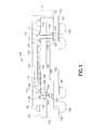
- FIG. 1is a cross-sectional view of a microelectronic package in accordance with one embodiment.
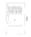
- FIG. 1Ais a top plan view of FIG. 2 .
- FIG. 2is a cross-sectional view of a microelectronic package in accordance with one embodiment.
- FIG. 2Ais a top plan view of FIG. 1 .
- FIG. 3is a cross-sectional view of an alternative embodiment of FIG. 1 .
- FIG. 4is a cross-sectional view of an alternative embodiment of FIG. 3 .
- FIG. 5is a cross-sectional view of an alternative embodiment of FIG. 4 .
- FIGS. 6 , 6 A, 6 B, 6 C, 6 D, and 6 Eillustrate cross-sectional views of a method of forming a microelectronic package of FIG. 1 , in accordance with one embodiment.
- FIGS. 7 , 7 A, 7 B, and 7 Cillustrate cross-sectional views of a method of forming a microelectronic package of FIG. 2 in accordance with one embodiment.
- FIG. 8is an alternative embodiment of a subassembly shown in FIG. 1 .
- FIG. 9is a cross-sectional view of a system incorporating an interconnection element.
- Microelectronic package 100includes a subassembly 101 attached to a substrate 192 , a monolithic encapsulant encapsulating the microelectric package 100 .
- the subassemblyincludes at least an element 102 , a first microelectronic element 130 , and a second microelectronic element 144 .
- Element 102has a coefficient of thermal expansion of less than 8 parts per million per degree Celsius (hereinafter, “ppm/° C.”) and can be used as an interconnection substrate to which other elements, e.g., microelectronic elements such as semiconductor chips, passive devices, e.g., capacitors, resistors or inductors, can be mounted and electrically connected therewith.
- element 102can include a bulk layer of semiconductor, glass, or ceramic material on which one or more metal or dielectric layers can be formed. Element 102 of this description can also be referred to as a “low CTE substrate.”
- Conductive elementsare provided in one or more metal layers of the low CTE substrate.
- Conductive elementsinclude a plurality of first contacts 108 and second contacts 110 exposed at the first surface 104 of element 102 and traces (not shown) which may extend along the first surface 104 , and which may or may not be exposed at the first surface.
- the plurality of contacts 108will have a fine pitch of 200 microns or less. Additional electrical features may include vias which electrically connect metal layers of the substrate to one another, when more than one metal layer is present.
- the conductive elementscan be formed from various electrically conductive materials, but most typically are formed from copper, copper alloys, nickel, aluminum, gold, titanium, titanium-tungsten-w, or other alloys of titanium, or combinations of these materials and/or other materials.
- an electrically conductive featurecan be considered “exposed at” a surface, such as at a surface of a dielectric layer that forms a top surface of a semiconductor chip, if the metallic feature is accessible to a contact or bonding material applied to such surface.
- a metallic feature which projects from the surface of the dielectric or which is flush with the surface of the dielectricis exposed at such surface; whereas a recessed conductive feature disposed in or aligned with a hole in the dielectric extending to the surface of the dielectric is also exposed at such surface.
- One or more aperturesmay extend between the first surface 104 and second surface 106 of the element 102 . As shown, there may be a first aperture 114 and second aperture 119 , but the number of apertures may be fewer or greater depending upon specific design considerations.
- the aperturesmay vary in size, but should be at least sufficiently large enough to enable conductive connections, including leads or wire bonds to extend therethrough.
- the aperturesmay be fabricated using low cost techniques such as by machining, ultrasonic drilling, particle blasting, wet etch, or any known techniques.
- Microelectronic elementseach of which may be base semiconductor chips, packaged semiconductor chips, or one or more semiconductor chips having an electrically conductive redistribution layer thereon, are attached to both the first and second surfaces 104 , 106 of the element 102 .
- a first microelectronic element 130mounted overlying the first surface 104 of the element 102 , has a front surface 132 facing the first surface 104 of the element 102 and an opposed rear surface 134 .
- Element contacts 131 exposed at the front surface 132face first contacts 108 on the first surface 104 and are joined to the first contacts 108 in a flip-chip orientation.
- electrically conductive bumps 136made of solder, tin, indium, gold, copper, conductive paste or a conductive matrix material, or other bond metal can join the element contacts of first microelectronic element 130 with the first contacts 108 .
- One or more second microelectronic elementsmay overlie the second surface 106 of element 102 and have contacts at the front surface of such second microelectronic element, which are aligned with one or more of the apertures 114 , 119 .
- wire bonds 174 Bcan extend through aperture 114 to electrically interconnect element contacts 148 of second microelectronic element 144 with second contacts 110 exposed at the first surface 104 of element 102 and adjacent aperture 114 .
- Any number of additional second microelectronic elementsmay be provided, such as the one additional second microelectronic element 150 shown in FIG. 1 , for example.
- Wire bonds 174 Belectrically connect element contacts 154 on the second microelectronic element 150 with second contacts 110 exposed at the first surface 104 of element 102 .
- the second microelectronic elements 144 , 150can be attached to the element 102 or to one another using a bonding material such as an adhesive.
- the respective edges of the second microelectronic elements 144 , 150may be staggered or offset, so that at least one edge of each of the second microelectronic elements 144 , 150 extends beyond the edge of a directly adjacent microelectronic element. Additionally, at least one edge of each of the microelectronic elements 144 , 150 is aligned with one of the first or second apertures 114 , 119 . In this embodiment, both the first edge 147 of the second microelectronic element 144 and the first edge 153 of the additional second microelectronic element 150 are aligned with the first aperture 114 . Wire bonds extending from respective element contacts 147 , 154 electrically connect with second contacts 110 on the element 102 . In alternative embodiments, the second microelectronic elements 144 , 150 may be arranged so that the element contacts are aligned with the second aperture 119 .
- the subassembly 101may be attached to substrate 192 using bonding material, such as an adhesive or the like deposited between the second microelectronic element 150 and the first surface 193 of the substrate 192 .
- Contacts 197 exposed at first surface 193 of the substrate 192may be electrically connected to third contacts 212 exposed at the first surface 104 of the element 102 using wire bonds 174 , 149 .
- wire bonds 174 , 149extend through aperture 119 and connect to third contacts 112 positioned adjacent aperture 119 .
- Terminals 195 exposed at the opposed second surface 194 of substrate 192may be provided to allow for interconnection to an external device such as a printed circuit board, another microelectronic package, or the like.
- FIG. 1Ais a top plan view of the microelectronic package 100 prior to encapsulation.
- the wafer subassembly 101 shown in FIG. 1Amay be fully encapsulated.
- an encapsulant 190such as an overmold ( FIG. 1 ) is deposited over the exposed first and second surfaces of the element 102 , first microelectronic elements 130 , second microelectronic elements 144 , 150 , each of the wire bonds 174 A-D, and through apertures 114 , 119 .
- microelectronic package 200includes a subassembly 201 , a substrate 292 with attached elements, and a monolithic encapsulant 290 that contacts exposed portions of subassembly 201 and substrate 292 .
- subassembly 201includes at least element 202 with a first microelectronic element 230 , attached thereto.
- Element 202has only one aperture 214 extending between first and second surfaces 204 , 206 .
- First contacts 208 and second contacts 210are exposed at a first surface 204 of element 202 , and second contacts 210 are positioned adjacent aperture 214 .
- First microelectronic element 230overlies element 202 so that front surface 232 of first microelectronic element 230 faces the first surface 204 of element 202 .
- Element contacts 231 exposed at front surface 232 of first microelectronic element 230are bonded to first contacts 208 using a bonding material, such as solder or the like.
- Passive components, such as capacitors 205may also be bonded to the first surface 204 of the element 202 .
- subassembly 201does not include second microelectronic elements stacked on the second surface 206 of element 202 .
- Second microelectronic element 244as well as another second microelectronic element 250 comprised of two chips 250 A, 250 B, are stacked to overlie the first surface 293 of substrate 292 .
- the stacked second microelectronic elements 244 , 250 A, 250 Bare attached to each other and the substrate 292 .
- each of the front surfaces 245 , 251 , 257 of the second microelectronic elementsface the element 202 but, as will be discussed, are wire bonded to substrate 292 .
- a spacer 291is provided between the element 202 and front surface 245 of second microelectronic element.
- second microelectronic elements 244 , 250 A, 250 Bare indirectly electrically connected to element 202 , as opposed to being directly wire-bonded to element 202 , as disclosed in the previous embodiment. As shown, each of second microelectronic elements 244 , 250 A, 250 B are directly connected to substrate 292 . In this embodiment, wire bonds extend from respective element contacts 248 , 254 , 260 on the respective microelectronic elements 244 , 250 A, 250 B to corresponding contacts exposed at the first surface 293 of substrate 292 .
- Wire bonds 274 Aextend between element contacts 248 exposed at the front surface of the second microelectronic element 244 and contacts 298 A exposed at substrate 292 ; wire bonds 274 B extend between element contacts 254 exposed at the front surface 251 of additional second microelectronic element 250 A and contacts 298 B exposed at substrate 292 ; and wire bonds 274 C extend between element contacts 260 exposed at front surface 257 of the additional second microelectronic element 250 B and contacts 298 C exposed at substrate 292 . There are also wire bonds 274 D, 274 E that electrically connect second contacts 210 on element 202 with contacts 297 exposed at the first surface 293 of substrate 292 .
- FIG. 2Aa schematic top plan view of the microelectronic package 200 prior to encapsulation, exposed rear surface 234 of first microelectronic element 230 is seen, as well as wire bonds 274 D-E extending through aperture 214 .
- An encapsulant 290( FIG. 2 ), such as an overmold, may be provided over each of the exposed surfaces of the components in the package. Encapsulant 290 covers the subassembly 201 , including at least first microelectronic element 230 , element 202 , and wire bonds 274 . Additionally, the encapsulant will cover the exposed components between the first surface 293 of the substrate 292 and the second surface 206 of the substrate 292 .
- the encapsulant 290covers or contacts exposed surfaces of the second microelectronic elements 244 , 250 A, 250 B, and corresponding wire bonds 274 A-C.
- the encapsulant 290is monolithic and contacts exposed surfaces of the components within the microelectronic package 200 .
- FIGS. 3-5illustrate a few examples of alternative embodiments, although it is to be appreciated that other arrangements that are not expressly illustrated herein are still contemplated within the scope of the presently disclosed invention.
- Subassembly 301includes first microelectronic element 330 overlying element 302 .
- the subassembly 301may be attached and electrically connected to stacked second microelectronic elements 344 , 350 , and substrate 392 through the use of wire bonds.
- Exposed surfaces of the microelectronic package 300can be encapsulated with a monolithic overmold 390 to provide a completed microelectronic packages 300 in accordance with this embodiment.
- the front surface 345 of second microelectronic element 344has element contacts exposed thereat and faces the second surface 306 of element 302 .
- Rear surface 346 of the second microelectronic element 344faces the rear surface 352 of the additional second microelectronic element 350 .
- the front surface of the additional second microelectronic element 350faces first surface 393 of substrate 392 .
- the additional second microelectronic element 350may be a DRAM chip or the like having element contacts 354 extending along a central portion of the microelectronic element 350 .
- This microelectronic package 300only differs from previous embodiments due to the stacked arrangement of second microelectronic elements 344 , 350 that overlie the second surface 306 of element 302 . As shown, the outer edges of the second microelectronic elements 344 , 350 are not staggered. Outer edges 147 A, 147 B of second microelectronic element 344 are instead aligned with edges 153 A, 153 B of the additional second microelectronic element 350 . Both second microelectronic elements 344 , 350 may be electrically connected to substrate 392 using wire bonds.
- the second microelectronic element 344may be electrically connected to the first surface 393 of the substrate 392 using wire bonds 374 A, 374 B extending from element contacts 348 on second microelectronic element 344 to contacts 398 A, 398 B exposed at the first surface 393 of substrate 392 .
- the additional second microelectronic element 350can be electrically connected to the second surface 394 of substrate 392 .
- wire bonds 374 C, 374 Dextend from contacts 354 exposed at the front surface 351 of the additional second microelectronic element 350 to contacts 398 C, 398 D exposed at the second surface 394 of substrate 392 .
- This particular stacked arrangementallows for the incorporation of a center-bonded microelectronic element 350 into the microelectronic package 300 .
- FIG. 4an alternative embodiment of FIG. 3 , a microelectronic package 400 is shown.
- the front surface 445 of the second microelectronic element 444faces element 402
- the front surface 451 of the additional second microelectronic element 450faces the first surface 493 of substrate 492 .
- the rear surface 452 of the additional second microelectronic element 450may be attached to the rear surface 446 of the second microelectronic element 444 .
- Element contacts 448 exposed at the front surface 445 of the second microelectronic element 444may be electrically connected to the substrate 492 via wire bonds 474 A, 474 B extending therebetween.
- This embodimentdiffers from the previous embodiments due to the stacked arrangement of the second microelectronic elements 444 , 450 that overlies substrate 492 .
- the additional second microelectronic 450is a D-RAM or center-bonded chip
- the additional second microelectronic element 450has element contacts 454 extending along its front surface 451 . This allows additional second microelectronic element 450 to be bonded in a flip-chip orientation to contacts 497 on the first surface 493 of substrate 492 .
- a monolithic encapsulant 490may be provided between the first surface 493 of the substrate 492 and the element 402 , as well as over the first surfaces of the element 402 and the surfaces of the devices thereon.
- microelectronic package 500in accordance with an alternative embodiment of FIG. 4 is shown.
- both second microelectronic element 544 , 550are mounted and electrically connected to the substrate 592 in a flip-chip orientation.
- the front surface 545 of the second microelectronic element 544may face the rear surface 552 of the additional second microelectronic element 550 .
- Conductive vias 542 extending between the front and rear surfaces 551 , 552 of the additional second microelectronic element 550allow for the second microelectronic element 544 to be electrically connected to the substrate 592 .
- Element contacts 548 exposed at the front surface 545 of the second microelectronic element 544may be electrically connected to conductive vias 542 . This can allow for electrical interconnection between the element contacts 548 and substrate 592 .
- a monolithic encapsulant 590such as overmold, may be provided over exposed surfaces.
- an element 102is provided with a plurality of contacts, such as first contacts 108 , second contacts 110 , and third contacts 112 exposed at a first surface 104 . Openings 114 , 119 , 114 ′, 119 ′ are created between the first surface and second surface, as shown in FIG. 6A .
- element 102may be inverted and a series of one or more second microelectronic elements may be attached thereto. Second microelectronic element 144 may be arranged to overlie the second surface 106 of the element 102 .
- second microelectronic element 144is attached to the second surface 106 of element 102 using a die attach, such as an adhesive (not shown).
- Another second microelectronic element 150may be attached to the rear surface of second microelectronic element 144 .
- second microelectronic elements 144 ′, 150 ′may also be attached to element 102 in the same manner. In this embodiment, if desired, once the second microelectronic elements 144 , 144 ′, 150 , 150 ′ are attached to element 102 , the integrity of second microelectronic elements 144 , 144 ′, 150 , 150 ′ can be tested.
- substrate 192is prepared with terminals on a second surface 194 and contacts 197 on the opposed first surface 193 .
- the substrate 192 and element 102 with attached second microelectronic elements 144 , 150are both inverted.
- Substrate 192is then attached to the rear surfaces of the additional second microelectronic elements 150 , 150 ′.
- first microelectronic element 130may then be provided on the first surface 102 of element 102 .
- first microelectronic element 130may be comprised of two chips 130 A′, 130 B′ that are arranged to overlie the first surface 104 of the element 104 in a flip-chip orientation.
- first microelectronic element 130is comprised of two semiconductor chips 130 A, 130 B, although one or more than two semiconductor chips may be utilized. Additionally, the one or more first microelectronic elements 130 may be arranged in any configuration over the element 102 , including, without limitation, a stacked configuration.
- first microelectronic element 130is tested prior to its assembly onto element 102 to avoid the cost of discovering a damaged or defective microelectronic element after the final assembly of the microelectronic package 100 ( FIG. 1 ). Testing of any of the microelectronic elements in the package can, of course, be conducted at any desired time.
- Wire bondsmay be incorporated into the package to provide an electrical interconnection between and among the first microelectronic elements 130 , 130 ′, second microelectronic elements 144 , 150 , 144 ′, 150 ′, substrate 192 , and element 102 .
- each of wire bonds 174 A, 174 A′extend through respective apertures 114 , 114 ′.
- wire bonds 174 B, 174 B′also extend through respective apertures 114 , 114 ′ These wire bonds connect second microelectronic elements 144 , 150 and 144 ′, 150 ′ with the first surface 104 of the element 102 .
- wire bonds 174 C, 174 D and 174 C′, 174 D′extend through respective apertures 119 , 119 ′ to directly connect substrate 192 with element 102 .
- an encapsulant 190may be provided over the exposed surfaces of components that are provided between the second surface 106 of the element 102 and first surface 193 of substrate 192 . Additionally, encapsulant 190 may cover exposed surfaces of the element 102 , components overlying the first surface 104 , wire bonds, and apertures 114 , 114 ′, 119 , 119 ′. Once the encapsulant 190 is cured, the wafer package may be cut along dicing line D-D, to provide the individual microelectronic package 100 shown in FIG. 1 .
- FIGS. 7-7Ca method of making the microelectronic package shown in FIG. 2 , in accordance with one embodiment is shown.
- Subassembly 201is shown in FIG. 7 , which is comprised of element 202 with apertures 214 , 214 ′ extending therethrough and first microelectronic elements 230 , 230 ′ electrically connected to contacts 208 exposed at the first surface 204 of element 202 .
- Passive elements, such as capacitors 205may also be provided on first surface 204 of element 202 .
- a substrate 292is provided with one aperture 214 extending therethrough, contacts 297 exposed at a first surface of substrate 292 , and terminals 295 exposed at a second surface of substrate 292 .
- Stacked second microelectronic elements 244 , 250 A, 250 Bmay be provided on the first surface 293 of substrate 292 .
- Rear surface 258 of additional second microelectronic element 250 Bmay be attached to first surface 293 of substrate 292 using a form of die attach, such as an adhesive (not shown).
- second microelectronic elements 244 , 250 A, 250 Bare arranged so that the edges 247 , 253 , 259 of each of the respective second microelectronic elements 244 , 250 A, 250 B are staggered to allow for element contacts 248 , 254 , and 260 to be exposed.
- Wire bonds 274 A, 274 B, 274 Cextend from respective element contacts 248 , 254 , and 260 to contacts exposed at the first surface 293 of substrate 292 .
- An encapsulant 290may be provided over each of the wire bonds 274 A, 274 B, 274 C. This identical arrangement can be utilized for the arrangement of second microelectronic elements 244 ′, 250 A′, 250 B′.
- substrate 292 with attached second microelectronic elements 244 , 250 A, 250 B, and 244 ′, 250 A′, 250 B′may be inverted and attached to second surface 206 of element 202 .
- spacers 291 , 291 ′may be provided between second surface 206 and front surfaces 245 , 245 ′ of second microelectronic elements 244 , 244 ′.
- Spacers 291 , 291 ′can provide space for the height of wire bond 274 A.
- Encapsulant 290 , 290 ′can also be attached to second surface 206 of element 202 .
- Apertures 214 , 214 ′should be aligned with contacts 297 exposed at the first surface 293 of substrate 292 .
- element 202may be electrically connected to contacts 297 through wire bonds 274 D, 274 D′, 274 E, 274 E′ that extend through apertures 214 , 214 ′.
- the assemblymay then be cut through line D-D to provide the individual microelectronic package 200 shown in FIG. 2 .
- the subassembly 601is similar to the subassembly 101 , shown in FIG. 1 , to the extent that it includes an element 602 with a first microelectronic element 630 electrically connected to contacts 108 exposed at the first surface 604 of element 602 , and second microelectronic elements 644 , 650 wire bonded through aperture 614 to contacts 610 exposed at the first surface of element 602 .
- element 602 of the subassembly 601further includes a second aperture 615 and third aperture 624 .
- second microelectronic elements 650 A, 650 Battached in a face-up orientation to the rear surface 652 of second microelectronic element 650 .
- the additional second microelectronic elements 650 A, 650 Bare staggered so that element contacts 660 , 666 of second microelectronic elements 650 A, 650 B can be aligned with aperture 615 in element 602 .
- Wire bonds 674 C, 674 Dextend through aperture 615 to electrically connect respective element contacts 660 , 666 with contacts 611 exposed at the first surface of element 602 .
- Another set of contacts 612 exposed at the first surface of element 602can be used to electrically connect element 602 with a substrate (not shown) when it is desired to incorporate subassembly 601 into a microelectronic package.
- a system 1000 in accordance with a further embodiment of the inventionincludes a structure 706 as described in the prior embodiments of microelectronic packages above in conjunction with other electronic components 708 and 710 .
- component 708is a semiconductor chip
- component 710is a display screen, but any other components can be used.
- the systemmay include any number of such components.
- the structure 706 as described abovemay be, for example, a composite chip or a structure incorporating plural chips. In a further variant, both may be provided, and any number of such structures may be used.
- Structure 706 and components 708 and 710are mounted in a common housing 701 , schematically depicted in broken lines, and are electrically interconnected with one another as necessary to form the desired circuit.
- the systemincludes a circuit panel 702 such as a flexible printed circuit board, and the circuit panel includes numerous conductors 704 , of which only one is depicted in FIG. 5 , interconnecting the components with one another.
- the housing 701is depicted as a portable housing of the type usable, for example, in a cellular telephone or personal digital assistant, and screen 710 is exposed at the surface of the housing.
- structure 706includes a light-sensitive element such as an imaging chip
- a lens 711 or other optical devicealso may be provided for routing light to the structure.
- FIG. 9the simplified system shown in FIG. 9 is merely exemplary; other systems, including systems commonly regarded as fixed structures, such as desktop computers, routers and the like can be made using the structures discussed above.
Landscapes
- Engineering & Computer Science (AREA)
- Microelectronics & Electronic Packaging (AREA)
- Power Engineering (AREA)
- Computer Hardware Design (AREA)
- Physics & Mathematics (AREA)
- Condensed Matter Physics & Semiconductors (AREA)
- General Physics & Mathematics (AREA)
- Ceramic Engineering (AREA)
- Manufacturing & Machinery (AREA)
- Wire Bonding (AREA)
- Structures For Mounting Electric Components On Printed Circuit Boards (AREA)
Abstract
Description
Claims (13)
Priority Applications (1)
| Application Number | Priority Date | Filing Date | Title |
|---|---|---|---|
| US13/216,465US8872318B2 (en) | 2011-08-24 | 2011-08-24 | Through interposer wire bond using low CTE interposer with coarse slot apertures |
Applications Claiming Priority (1)
| Application Number | Priority Date | Filing Date | Title |
|---|---|---|---|
| US13/216,465US8872318B2 (en) | 2011-08-24 | 2011-08-24 | Through interposer wire bond using low CTE interposer with coarse slot apertures |
Publications (2)
| Publication Number | Publication Date |
|---|---|
| US20130049196A1 US20130049196A1 (en) | 2013-02-28 |
| US8872318B2true US8872318B2 (en) | 2014-10-28 |
Family
ID=47742471
Family Applications (1)
| Application Number | Title | Priority Date | Filing Date |
|---|---|---|---|
| US13/216,465Active2032-11-02US8872318B2 (en) | 2011-08-24 | 2011-08-24 | Through interposer wire bond using low CTE interposer with coarse slot apertures |
Country Status (1)
| Country | Link |
|---|---|
| US (1) | US8872318B2 (en) |
Cited By (3)
| Publication number | Priority date | Publication date | Assignee | Title |
|---|---|---|---|---|
| US20190088565A1 (en)* | 2017-06-13 | 2019-03-21 | Micron Technology, Inc. | Face Down Dual Sided Chip Scale Memory Package |
| US20210159090A1 (en)* | 2018-04-11 | 2021-05-27 | Advanced Semiconductor Engineering, Inc. | Semiconductor device package and method of manufacturing the same |
| US20220223504A1 (en)* | 2021-01-08 | 2022-07-14 | Jmj Korea Co., Ltd. | Semiconductor package |
Families Citing this family (1)
| Publication number | Priority date | Publication date | Assignee | Title |
|---|---|---|---|---|
| US11270963B2 (en) | 2020-01-14 | 2022-03-08 | Sandisk Technologies Llc | Bonding pads including interfacial electromigration barrier layers and methods of making the same |
Citations (142)
| Publication number | Priority date | Publication date | Assignee | Title |
|---|---|---|---|---|
| US3900153A (en) | 1972-06-13 | 1975-08-19 | Licentia Gmbh | Formation of solder layers |
| US4695870A (en) | 1986-03-27 | 1987-09-22 | Hughes Aircraft Company | Inverted chip carrier |
| US4716049A (en) | 1985-12-20 | 1987-12-29 | Hughes Aircraft Company | Compressive pedestal for microminiature connections |
| US4804132A (en) | 1987-08-28 | 1989-02-14 | Difrancesco Louis | Method for cold bonding |
| US4878611A (en) | 1986-05-30 | 1989-11-07 | American Telephone And Telegraph Company, At&T Bell Laboratories | Process for controlling solder joint geometry when surface mounting a leadless integrated circuit package on a substrate |
| US4902600A (en) | 1986-10-14 | 1990-02-20 | Fuji Photo Film Co., Ltd. | Light-sensitive material comprising light-sensitive layer provided on support wherein the light-sensitive layer and support have specified pH values |
| US4924353A (en) | 1985-12-20 | 1990-05-08 | Hughes Aircraft Company | Connector system for coupling to an integrated circuit chip |
| US4975079A (en) | 1990-02-23 | 1990-12-04 | International Business Machines Corp. | Connector assembly for chip testing |
| US4982265A (en) | 1987-06-24 | 1991-01-01 | Hitachi, Ltd. | Semiconductor integrated circuit device and method of manufacturing the same |
| US5083697A (en) | 1990-02-14 | 1992-01-28 | Difrancesco Louis | Particle-enhanced joining of metal surfaces |
| US5138438A (en) | 1987-06-24 | 1992-08-11 | Akita Electronics Co. Ltd. | Lead connections means for stacked tab packaged IC chips |
| US5148266A (en) | 1990-09-24 | 1992-09-15 | Ist Associates, Inc. | Semiconductor chip assemblies having interposer and flexible lead |
| US5148265A (en) | 1990-09-24 | 1992-09-15 | Ist Associates, Inc. | Semiconductor chip assemblies with fan-in leads |
| US5186381A (en) | 1991-04-16 | 1993-02-16 | Samsung Electronics, Co., Ltd. | Semiconductor chip bonding process |
| US5189505A (en) | 1989-11-08 | 1993-02-23 | Hewlett-Packard Company | Flexible attachment flip-chip assembly |
| US5196726A (en) | 1990-01-23 | 1993-03-23 | Sumitomo Electric Industries, Ltd. | Substrate for packaging a semiconductor device having particular terminal and bump structure |
| US5214308A (en) | 1990-01-23 | 1993-05-25 | Sumitomo Electric Industries, Ltd. | Substrate for packaging a semiconductor device |
| US5222014A (en) | 1992-03-02 | 1993-06-22 | Motorola, Inc. | Three-dimensional multi-chip pad array carrier |
| US5247423A (en) | 1992-05-26 | 1993-09-21 | Motorola, Inc. | Stacking three dimensional leadless multi-chip module and method for making the same |
| US5340771A (en) | 1993-03-18 | 1994-08-23 | Lsi Logic Corporation | Techniques for providing high I/O count connections to semiconductor dies |
| US5397997A (en) | 1991-08-23 | 1995-03-14 | Nchip, Inc. | Burn-in technologies for unpackaged integrated circuits |
| US5422435A (en) | 1992-05-22 | 1995-06-06 | National Semiconductor Corporation | Stacked multi-chip modules and method of manufacturing |
| US5455390A (en) | 1994-02-01 | 1995-10-03 | Tessera, Inc. | Microelectronics unit mounting with multiple lead bonding |
| US5518964A (en) | 1994-07-07 | 1996-05-21 | Tessera, Inc. | Microelectronic mounting with multiple lead deformation and bonding |
| US5615824A (en) | 1994-06-07 | 1997-04-01 | Tessera, Inc. | Soldering with resilient contacts |
| US5656550A (en) | 1994-08-24 | 1997-08-12 | Fujitsu Limited | Method of producing a semicondutor device having a lead portion with outer connecting terminal |
| US5659952A (en) | 1994-09-20 | 1997-08-26 | Tessera, Inc. | Method of fabricating compliant interface for semiconductor chip |
| US5679977A (en) | 1990-09-24 | 1997-10-21 | Tessera, Inc. | Semiconductor chip assemblies, methods of making same and components for same |
| US5731709A (en) | 1996-01-26 | 1998-03-24 | Motorola, Inc. | Method for testing a ball grid array semiconductor device and a device for such testing |
| US5736780A (en) | 1995-11-07 | 1998-04-07 | Shinko Electric Industries Co., Ltd. | Semiconductor device having circuit pattern along outer periphery of sealing resin and related processes |
| US5802699A (en) | 1994-06-07 | 1998-09-08 | Tessera, Inc. | Methods of assembling microelectronic assembly with socket for engaging bump leads |
| US5811982A (en) | 1995-11-27 | 1998-09-22 | International Business Machines Corporation | High density cantilevered probe for electronic devices |
| US5854507A (en) | 1998-07-21 | 1998-12-29 | Hewlett-Packard Company | Multiple chip assembly |
| US5912505A (en) | 1995-11-07 | 1999-06-15 | Sumitomo Metal (Smi) Electronics Devices, Inc. | Semiconductor package and semiconductor device |
| US5973391A (en) | 1997-12-11 | 1999-10-26 | Read-Rite Corporation | Interposer with embedded circuitry and method for using the same to package microelectronic units |
| US5971253A (en) | 1995-07-31 | 1999-10-26 | Tessera, Inc. | Microelectronic component mounting with deformable shell terminals |
| US5998864A (en) | 1995-05-26 | 1999-12-07 | Formfactor, Inc. | Stacking semiconductor devices, particularly memory chips |
| US6032359A (en) | 1997-08-21 | 2000-03-07 | Carroll; Keith C. | Method of manufacturing a female electrical connector in a single layer flexible polymeric dielectric film substrate |
| US6038136A (en) | 1997-10-29 | 2000-03-14 | Hestia Technologies, Inc. | Chip package with molded underfill |
| US6052287A (en) | 1997-12-09 | 2000-04-18 | Sandia Corporation | Silicon ball grid array chip carrier |
| US6054756A (en) | 1992-07-24 | 2000-04-25 | Tessera, Inc. | Connection components with frangible leads and bus |
| US6077380A (en) | 1995-06-30 | 2000-06-20 | Microfab Technologies, Inc. | Method of forming an adhesive connection |
| US6124546A (en) | 1997-12-03 | 2000-09-26 | Advanced Micro Devices, Inc. | Integrated circuit chip package and method of making the same |
| US6177636B1 (en) | 1994-12-29 | 2001-01-23 | Tessera, Inc. | Connection components with posts |
| US6194250B1 (en) | 1998-09-14 | 2001-02-27 | Motorola, Inc. | Low-profile microelectronic package |
| US6202297B1 (en) | 1995-08-28 | 2001-03-20 | Tessera, Inc. | Socket for engaging bump leads on a microelectronic device and methods therefor |
| US6258625B1 (en) | 1999-05-18 | 2001-07-10 | International Business Machines Corporation | Method of interconnecting electronic components using a plurality of conductive studs |
| US6300163B1 (en)* | 1996-06-26 | 2001-10-09 | Micron Technology, Inc. | Stacked leads-over-chip multi-chip module |
| DE10023823A1 (en) | 2000-05-15 | 2001-12-06 | Infineon Technologies Ag | Multi-chip housing device has carrier supporting stacked chip components with lowermost chip component having contact coupled to terminal surface of carrier |
| US6332270B2 (en) | 1998-11-23 | 2001-12-25 | International Business Machines Corporation | Method of making high density integral test probe |
| US6358627B2 (en) | 1999-04-03 | 2002-03-19 | International Business Machines Corporation | Rolling ball connector |
| US6362525B1 (en) | 1999-11-09 | 2002-03-26 | Cypress Semiconductor Corp. | Circuit structure including a passive element formed within a grid array substrate and method for making the same |
| US20020043709A1 (en) | 2000-10-13 | 2002-04-18 | Yeh Nai Hua | Stackable integrated circuit |
| US20020053727A1 (en) | 2000-08-31 | 2002-05-09 | Naoto Kimura | Semiconductor device |
| US20020074630A1 (en) | 1999-11-30 | 2002-06-20 | Fujitsu Limited | Semiconductor device having protruding electrodes higher than a sealed portion |
| US6445594B1 (en) | 2000-02-10 | 2002-09-03 | Mitsubishi Denki Kabushiki Kaisha | Semiconductor device having stacked semiconductor elements |
| US20020121687A1 (en) | 2001-03-02 | 2002-09-05 | Johann Winderl | Electronic component with stacked semiconductor chips |
| US20020125571A1 (en) | 1998-06-30 | 2002-09-12 | Corisis David J. | Module assembly for stacked BGA packages |
| US6458411B1 (en) | 2001-01-17 | 2002-10-01 | Aralight, Inc. | Method of making a mechanically compliant bump |
| US20020153602A1 (en) | 2000-05-16 | 2002-10-24 | Tay Wuu Yean | Ball grid array chip packages having improved testing and stacking characteristics |
| US6495914B1 (en) | 1997-08-19 | 2002-12-17 | Hitachi, Ltd. | Multi-chip module structure having conductive blocks to provide electrical connection between conductors on first and second sides of a conductive base substrate |
| US20020190396A1 (en) | 2000-08-16 | 2002-12-19 | Brand Joseph M. | Method and apparatus for removing encapsulating material from a packaged microelectronic device |
| US6507098B1 (en)* | 1999-08-05 | 2003-01-14 | Siliconware Precision Industries Co., Ltd. | Multi-chip packaging structure |
| US6507104B2 (en) | 2000-09-07 | 2003-01-14 | Siliconware Precision Industries Co., Ltd. | Semiconductor package with embedded heat-dissipating device |
| US6515355B1 (en) | 1998-09-02 | 2003-02-04 | Micron Technology, Inc. | Passivation layer for packaged integrated circuits |
| US6514847B1 (en) | 1997-11-28 | 2003-02-04 | Sony Corporation | Method for making a semiconductor device |
| US20030057544A1 (en) | 2001-09-13 | 2003-03-27 | Nathan Richard J. | Integrated assembly protocol |
| US6545228B2 (en) | 2000-09-05 | 2003-04-08 | Seiko Epson Corporation | Semiconductor device with a plurality of stacked boards and method of making |
| US6550666B2 (en) | 2001-08-21 | 2003-04-22 | Advanpack Solutions Pte Ltd | Method for forming a flip chip on leadframe semiconductor package |
| US6555918B2 (en) | 1997-09-29 | 2003-04-29 | Hitachi, Ltd. | Stacked semiconductor device including improved lead frame arrangement |
| US6560117B2 (en) | 2000-06-28 | 2003-05-06 | Micron Technology, Inc. | Packaged microelectronic die assemblies and methods of manufacture |
| US6573458B1 (en) | 1998-09-07 | 2003-06-03 | Ngk Spark Plug Co., Ltd. | Printed circuit board |
| US20030102546A1 (en) | 2001-04-17 | 2003-06-05 | Lee Teck Kheng | Method and apparatus for package reduction in stacked chip and board assemblies |
| US6578754B1 (en) | 2000-04-27 | 2003-06-17 | Advanpack Solutions Pte. Ltd. | Pillar connections for semiconductor chips and method of manufacture |
| US20030124767A1 (en) | 2001-12-31 | 2003-07-03 | Jin-Yuan Lee | Integrated chip package structure using ceramic substrate and method of manufacturing the same |
| US20030164540A1 (en) | 2002-03-04 | 2003-09-04 | Lee Teck Kheng | Semiconductor die packages with recessed interconnecting structures and methods for assembling the same |
| US6624653B1 (en) | 2000-08-28 | 2003-09-23 | Micron Technology, Inc. | Method and system for wafer level testing and burning-in semiconductor components |
| US20030183930A1 (en) | 2001-07-04 | 2003-10-02 | Hiroyuki Fukasawa | Semiconductor device and semiconductor module |
| US6647310B1 (en) | 2000-05-30 | 2003-11-11 | Advanced Micro Devices, Inc. | Temperature control of an integrated circuit |
| US20040026773A1 (en) | 2002-08-08 | 2004-02-12 | Koon Eng Meow | Packaged microelectronic components |
| US20040038447A1 (en) | 2002-08-21 | 2004-02-26 | Corisis David J | Packaged microelectronic devices and methods for assembling microelectronic devices |
| US20040036164A1 (en) | 2001-07-31 | 2004-02-26 | Toshihiko Koike | Semiconductor device and its manufacturing method |
| US20040061211A1 (en)* | 2002-10-01 | 2004-04-01 | Mitsubishi Denki Kabushiki Kaisha | Semiconductor package |
| US20040075164A1 (en) | 2002-10-18 | 2004-04-22 | Siliconware Precision Industries, Ltd. | Module device of stacked semiconductor packages and method for fabricating the same |
| US20040090756A1 (en) | 2002-11-07 | 2004-05-13 | Kwun-Yo Ho | Chip packaging structure and manufacturing process thereof |
| US20040090759A1 (en) | 2002-10-24 | 2004-05-13 | Jin-Ho Kim | Multi-package stack module |
| US20040110319A1 (en) | 1994-03-18 | 2004-06-10 | Hitachi Chemical Company, Ltd. | Fabrication process of semiconductor package and semiconductor package |
| US6762488B2 (en)* | 2002-03-19 | 2004-07-13 | Nec Electronics Corporation | Light thin stacked package semiconductor device and process for fabrication thereof |
| US6765287B1 (en) | 2001-07-27 | 2004-07-20 | Charles W. C. Lin | Three-dimensional stacked semiconductor package |
| US20040160751A1 (en) | 1999-09-02 | 2004-08-19 | Ibiden Co., Ltd. | Printed circuit board and method of manufacturing printed circuit board |
| US20040262734A1 (en) | 2003-06-30 | 2004-12-30 | Cheol-Joon Yoo | Stack type ball grid array package and method for manufacturing the same |
| US20050035440A1 (en) | 2001-08-22 | 2005-02-17 | Tessera, Inc. | Stacked chip assembly with stiffening layer |
| US6861288B2 (en)* | 2003-01-23 | 2005-03-01 | St Assembly Test Services, Ltd. | Stacked semiconductor packages and method for the fabrication thereof |
| US20050082664A1 (en) | 2003-10-16 | 2005-04-21 | Elpida Memory, Inc. | Stacked semiconductor device and semiconductor chip control method |
| US20050104196A1 (en) | 2003-11-18 | 2005-05-19 | Denso Corporation | Semiconductor package |
| US20050116326A1 (en) | 2003-10-06 | 2005-06-02 | Tessera, Inc. | Formation of circuitry with modification of feature height |
| US6902869B2 (en) | 1997-11-12 | 2005-06-07 | International Business Machines Corporation | Manufacturing methods for printed circuit boards |
| US20050173805A1 (en) | 2003-12-30 | 2005-08-11 | Tessera, Inc. | Micro pin grid array with pin motion isolation |
| US6930256B1 (en) | 2002-05-01 | 2005-08-16 | Amkor Technology, Inc. | Integrated circuit substrate having laser-embedded conductive patterns and method therefor |
| US20050181655A1 (en) | 2003-12-30 | 2005-08-18 | Tessera, Inc. | Micro pin grid array with wiping action |
| US20050181544A1 (en) | 2003-12-30 | 2005-08-18 | Tessera, Inc. | Microelectronic packages and methods therefor |
| US20050285246A1 (en) | 2004-06-25 | 2005-12-29 | Tessera, Inc. | Microelectronic packages and methods therefor |
| US20050284658A1 (en) | 2003-10-06 | 2005-12-29 | Tessera, Inc. | Components with posts and pads |
| US6987032B1 (en) | 2002-07-19 | 2006-01-17 | Asat Ltd. | Ball grid array package and process for manufacturing same |
| US7045884B2 (en) | 2002-10-04 | 2006-05-16 | International Rectifier Corporation | Semiconductor device package |
| US7067911B1 (en) | 2000-10-13 | 2006-06-27 | Bridge Semiconductor Corporation | Three-dimensional stacked semiconductor package with metal pillar in encapsulant aperture |
| US20060172457A1 (en)* | 2005-02-02 | 2006-08-03 | Siliconware Precision Industries Co., Ltd. | Chip-stacked semiconductor package and method for fabricating the same |
| US20060202317A1 (en) | 2005-03-14 | 2006-09-14 | Farid Barakat | Method for MCP packaging for balanced performance |
| US20060290005A1 (en) | 2005-06-28 | 2006-12-28 | Jochen Thomas | Multi-chip device and method for producing a multi-chip device |
| US7176559B2 (en) | 2002-08-16 | 2007-02-13 | Via Technologies, Inc. | Integrated circuit package with a balanced-part structure |
| US7205656B2 (en)* | 2005-02-22 | 2007-04-17 | Micron Technology, Inc. | Stacked device package for peripheral and center device pad layout device |
| US7215033B2 (en) | 2003-11-19 | 2007-05-08 | Samsung Electronics Co., Ltd. | Wafer level stack structure for system-in-package and method thereof |
| US7233057B2 (en) | 2004-05-28 | 2007-06-19 | Nokia Corporation | Integrated circuit package with optimized mold shape |
| US20070148822A1 (en) | 2005-12-23 | 2007-06-28 | Tessera, Inc. | Microelectronic packages and methods therefor |
| US20070222054A1 (en)* | 2005-04-08 | 2007-09-27 | Hembree David R | Semiconductor components with through wire interconnects |
| US20070252260A1 (en)* | 2006-04-28 | 2007-11-01 | Micron Technology, Inc. | Stacked die packages |
| US7323767B2 (en) | 2002-04-25 | 2008-01-29 | Micron Technology, Inc. | Standoffs for centralizing internals in packaging process |
| US20080042249A1 (en)* | 2006-08-16 | 2008-02-21 | Tessera, Inc. | Microelectronic package |
| US20080105984A1 (en)* | 2006-11-03 | 2008-05-08 | Samsung Electronics Co., Ltd. | Semiconductor chip stack package with reinforcing member for preventing package warpage connected to substrate |
| US7372151B1 (en) | 2003-09-12 | 2008-05-13 | Asat Ltd. | Ball grid array package and process for manufacturing same |
| US20080136005A1 (en) | 2006-12-09 | 2008-06-12 | Stats Chippac Ltd. | Stackable integrated circuit package system |
| US7408245B2 (en)* | 2006-12-22 | 2008-08-05 | Powertech Technology Inc. | IC package encapsulating a chip under asymmetric single-side leads |
| US20080284045A1 (en) | 2007-05-18 | 2008-11-20 | Texas Instruments Incorporated | Method for Fabricating Array-Molded Package-On-Package |
| US20080315385A1 (en) | 2007-06-22 | 2008-12-25 | Texas Instruments Incorporated | Array molded package-on-package having redistribution lines |
| US7485562B2 (en) | 2002-08-27 | 2009-02-03 | Micron Technology, Inc. | Method of making multichip wafer level packages and computing systems incorporating same |
| US20090045524A1 (en)* | 2007-08-16 | 2009-02-19 | Tessera, Inc. | Microelectronic package |
| US7514776B2 (en)* | 2001-03-15 | 2009-04-07 | Micron Technology, Inc. | Semiconductor/printed circuit board assembly, and computer system |
| US20090104736A1 (en) | 2004-11-03 | 2009-04-23 | Tessera, Inc. | Stacked Packaging Improvements |
| US20090115043A1 (en)* | 2007-11-01 | 2009-05-07 | Seng Guan Chow | Mountable integrated circuit package system with mounting interconnects |
| US20090189293A1 (en)* | 2008-01-09 | 2009-07-30 | Elpida Memory, Inc. | Semiconductor device |
| US20090256267A1 (en)* | 2008-04-11 | 2009-10-15 | Yang Deokkyung | Integrated circuit package-on-package system with central bond wires |
| US7633765B1 (en) | 2004-03-23 | 2009-12-15 | Amkor Technology, Inc. | Semiconductor package including a top-surface metal layer for implementing circuit features |
| US7638880B2 (en)* | 2006-03-17 | 2009-12-29 | Chipmos Technologies Inc. | Chip package |
| US7671459B2 (en) | 2006-02-08 | 2010-03-02 | Micron Technologies, Inc. | Microelectronic devices, stacked microelectronic devices, and methods for manufacturing such devices |
| US7675152B2 (en) | 2005-09-01 | 2010-03-09 | Texas Instruments Incorporated | Package-on-package semiconductor assembly |
| US20100084754A1 (en)* | 2007-06-12 | 2010-04-08 | Samsung Electro-Mechanics Co., Ltd | Semiconductor package |
| US7763961B2 (en)* | 2006-04-01 | 2010-07-27 | Stats Chippac Ltd. | Hybrid stacking package system |
| US20100264521A1 (en)* | 2005-12-07 | 2010-10-21 | Wood Alan G | Semiconductor Component Having Through Wire Interconnect (TWI) With Compressed Wire |
| US7911046B2 (en)* | 2007-02-06 | 2011-03-22 | Stats Chippac Ltd. | Integrated circuit packaging system with interposer |
| US20110169154A1 (en)* | 2006-05-12 | 2011-07-14 | Micron Technology, Inc. | Microelectronic devices and methods for manufacturing microelectronic devices |
| US20110266652A1 (en)* | 2008-03-13 | 2011-11-03 | Stats Chippac, Ltd. | Semiconductor Package with Penetrable Encapsulant Joining Semiconductor Die and Method Thereof |
| US8111523B2 (en)* | 2008-01-31 | 2012-02-07 | Shinko Electric Industries Co., Ltd. | Wiring board with switching function and method of manufacturing the same |
- 2011
- 2011-08-24USUS13/216,465patent/US8872318B2/enactiveActive
Patent Citations (149)
| Publication number | Priority date | Publication date | Assignee | Title |
|---|---|---|---|---|
| US3900153A (en) | 1972-06-13 | 1975-08-19 | Licentia Gmbh | Formation of solder layers |
| US4716049A (en) | 1985-12-20 | 1987-12-29 | Hughes Aircraft Company | Compressive pedestal for microminiature connections |
| US4924353A (en) | 1985-12-20 | 1990-05-08 | Hughes Aircraft Company | Connector system for coupling to an integrated circuit chip |
| US4695870A (en) | 1986-03-27 | 1987-09-22 | Hughes Aircraft Company | Inverted chip carrier |
| US4878611A (en) | 1986-05-30 | 1989-11-07 | American Telephone And Telegraph Company, At&T Bell Laboratories | Process for controlling solder joint geometry when surface mounting a leadless integrated circuit package on a substrate |
| US4902600A (en) | 1986-10-14 | 1990-02-20 | Fuji Photo Film Co., Ltd. | Light-sensitive material comprising light-sensitive layer provided on support wherein the light-sensitive layer and support have specified pH values |
| US5138438A (en) | 1987-06-24 | 1992-08-11 | Akita Electronics Co. Ltd. | Lead connections means for stacked tab packaged IC chips |
| US4982265A (en) | 1987-06-24 | 1991-01-01 | Hitachi, Ltd. | Semiconductor integrated circuit device and method of manufacturing the same |
| US4804132A (en) | 1987-08-28 | 1989-02-14 | Difrancesco Louis | Method for cold bonding |
| US5189505A (en) | 1989-11-08 | 1993-02-23 | Hewlett-Packard Company | Flexible attachment flip-chip assembly |
| US5214308A (en) | 1990-01-23 | 1993-05-25 | Sumitomo Electric Industries, Ltd. | Substrate for packaging a semiconductor device |
| US5196726A (en) | 1990-01-23 | 1993-03-23 | Sumitomo Electric Industries, Ltd. | Substrate for packaging a semiconductor device having particular terminal and bump structure |
| US5083697A (en) | 1990-02-14 | 1992-01-28 | Difrancesco Louis | Particle-enhanced joining of metal surfaces |
| US4975079A (en) | 1990-02-23 | 1990-12-04 | International Business Machines Corp. | Connector assembly for chip testing |
| US5148265A (en) | 1990-09-24 | 1992-09-15 | Ist Associates, Inc. | Semiconductor chip assemblies with fan-in leads |
| US5148266A (en) | 1990-09-24 | 1992-09-15 | Ist Associates, Inc. | Semiconductor chip assemblies having interposer and flexible lead |
| US5679977A (en) | 1990-09-24 | 1997-10-21 | Tessera, Inc. | Semiconductor chip assemblies, methods of making same and components for same |
| US5186381A (en) | 1991-04-16 | 1993-02-16 | Samsung Electronics, Co., Ltd. | Semiconductor chip bonding process |
| US5397997A (en) | 1991-08-23 | 1995-03-14 | Nchip, Inc. | Burn-in technologies for unpackaged integrated circuits |
| US5222014A (en) | 1992-03-02 | 1993-06-22 | Motorola, Inc. | Three-dimensional multi-chip pad array carrier |
| US5495398A (en) | 1992-05-22 | 1996-02-27 | National Semiconductor Corporation | Stacked multi-chip modules and method of manufacturing |
| US5422435A (en) | 1992-05-22 | 1995-06-06 | National Semiconductor Corporation | Stacked multi-chip modules and method of manufacturing |
| US5502289A (en) | 1992-05-22 | 1996-03-26 | National Semiconductor Corporation | Stacked multi-chip modules and method of manufacturing |
| US5247423A (en) | 1992-05-26 | 1993-09-21 | Motorola, Inc. | Stacking three dimensional leadless multi-chip module and method for making the same |
| US6054756A (en) | 1992-07-24 | 2000-04-25 | Tessera, Inc. | Connection components with frangible leads and bus |
| US5340771A (en) | 1993-03-18 | 1994-08-23 | Lsi Logic Corporation | Techniques for providing high I/O count connections to semiconductor dies |
| US5455390A (en) | 1994-02-01 | 1995-10-03 | Tessera, Inc. | Microelectronics unit mounting with multiple lead bonding |
| US20040110319A1 (en) | 1994-03-18 | 2004-06-10 | Hitachi Chemical Company, Ltd. | Fabrication process of semiconductor package and semiconductor package |
| US5802699A (en) | 1994-06-07 | 1998-09-08 | Tessera, Inc. | Methods of assembling microelectronic assembly with socket for engaging bump leads |
| US5615824A (en) | 1994-06-07 | 1997-04-01 | Tessera, Inc. | Soldering with resilient contacts |
| US5980270A (en) | 1994-06-07 | 1999-11-09 | Tessera, Inc. | Soldering with resilient contacts |
| US5518964A (en) | 1994-07-07 | 1996-05-21 | Tessera, Inc. | Microelectronic mounting with multiple lead deformation and bonding |
| US5656550A (en) | 1994-08-24 | 1997-08-12 | Fujitsu Limited | Method of producing a semicondutor device having a lead portion with outer connecting terminal |
| US5659952A (en) | 1994-09-20 | 1997-08-26 | Tessera, Inc. | Method of fabricating compliant interface for semiconductor chip |
| US6177636B1 (en) | 1994-12-29 | 2001-01-23 | Tessera, Inc. | Connection components with posts |
| US5998864A (en) | 1995-05-26 | 1999-12-07 | Formfactor, Inc. | Stacking semiconductor devices, particularly memory chips |
| US6077380A (en) | 1995-06-30 | 2000-06-20 | Microfab Technologies, Inc. | Method of forming an adhesive connection |
| US5971253A (en) | 1995-07-31 | 1999-10-26 | Tessera, Inc. | Microelectronic component mounting with deformable shell terminals |
| US6202297B1 (en) | 1995-08-28 | 2001-03-20 | Tessera, Inc. | Socket for engaging bump leads on a microelectronic device and methods therefor |
| US5736780A (en) | 1995-11-07 | 1998-04-07 | Shinko Electric Industries Co., Ltd. | Semiconductor device having circuit pattern along outer periphery of sealing resin and related processes |
| US5912505A (en) | 1995-11-07 | 1999-06-15 | Sumitomo Metal (Smi) Electronics Devices, Inc. | Semiconductor package and semiconductor device |
| US5811982A (en) | 1995-11-27 | 1998-09-22 | International Business Machines Corporation | High density cantilevered probe for electronic devices |
| US5731709A (en) | 1996-01-26 | 1998-03-24 | Motorola, Inc. | Method for testing a ball grid array semiconductor device and a device for such testing |
| US6300163B1 (en)* | 1996-06-26 | 2001-10-09 | Micron Technology, Inc. | Stacked leads-over-chip multi-chip module |
| US6495914B1 (en) | 1997-08-19 | 2002-12-17 | Hitachi, Ltd. | Multi-chip module structure having conductive blocks to provide electrical connection between conductors on first and second sides of a conductive base substrate |
| US6032359A (en) | 1997-08-21 | 2000-03-07 | Carroll; Keith C. | Method of manufacturing a female electrical connector in a single layer flexible polymeric dielectric film substrate |
| US6555918B2 (en) | 1997-09-29 | 2003-04-29 | Hitachi, Ltd. | Stacked semiconductor device including improved lead frame arrangement |
| US6038136A (en) | 1997-10-29 | 2000-03-14 | Hestia Technologies, Inc. | Chip package with molded underfill |
| US6902869B2 (en) | 1997-11-12 | 2005-06-07 | International Business Machines Corporation | Manufacturing methods for printed circuit boards |
| US6514847B1 (en) | 1997-11-28 | 2003-02-04 | Sony Corporation | Method for making a semiconductor device |
| US6124546A (en) | 1997-12-03 | 2000-09-26 | Advanced Micro Devices, Inc. | Integrated circuit chip package and method of making the same |
| US6052287A (en) | 1997-12-09 | 2000-04-18 | Sandia Corporation | Silicon ball grid array chip carrier |
| US5973391A (en) | 1997-12-11 | 1999-10-26 | Read-Rite Corporation | Interposer with embedded circuitry and method for using the same to package microelectronic units |
| US20020125571A1 (en) | 1998-06-30 | 2002-09-12 | Corisis David J. | Module assembly for stacked BGA packages |
| US5854507A (en) | 1998-07-21 | 1998-12-29 | Hewlett-Packard Company | Multiple chip assembly |
| US6515355B1 (en) | 1998-09-02 | 2003-02-04 | Micron Technology, Inc. | Passivation layer for packaged integrated circuits |
| US6573458B1 (en) | 1998-09-07 | 2003-06-03 | Ngk Spark Plug Co., Ltd. | Printed circuit board |
| US6194250B1 (en) | 1998-09-14 | 2001-02-27 | Motorola, Inc. | Low-profile microelectronic package |
| US6332270B2 (en) | 1998-11-23 | 2001-12-25 | International Business Machines Corporation | Method of making high density integral test probe |
| US6358627B2 (en) | 1999-04-03 | 2002-03-19 | International Business Machines Corporation | Rolling ball connector |
| US6258625B1 (en) | 1999-05-18 | 2001-07-10 | International Business Machines Corporation | Method of interconnecting electronic components using a plurality of conductive studs |
| US6507098B1 (en)* | 1999-08-05 | 2003-01-14 | Siliconware Precision Industries Co., Ltd. | Multi-chip packaging structure |
| US20040160751A1 (en) | 1999-09-02 | 2004-08-19 | Ibiden Co., Ltd. | Printed circuit board and method of manufacturing printed circuit board |
| US6362525B1 (en) | 1999-11-09 | 2002-03-26 | Cypress Semiconductor Corp. | Circuit structure including a passive element formed within a grid array substrate and method for making the same |
| US20020074630A1 (en) | 1999-11-30 | 2002-06-20 | Fujitsu Limited | Semiconductor device having protruding electrodes higher than a sealed portion |
| US6445594B1 (en) | 2000-02-10 | 2002-09-03 | Mitsubishi Denki Kabushiki Kaisha | Semiconductor device having stacked semiconductor elements |
| US6578754B1 (en) | 2000-04-27 | 2003-06-17 | Advanpack Solutions Pte. Ltd. | Pillar connections for semiconductor chips and method of manufacture |
| DE10023823A1 (en) | 2000-05-15 | 2001-12-06 | Infineon Technologies Ag | Multi-chip housing device has carrier supporting stacked chip components with lowermost chip component having contact coupled to terminal surface of carrier |
| US6522018B1 (en) | 2000-05-16 | 2003-02-18 | Micron Technology, Inc. | Ball grid array chip packages having improved testing and stacking characteristics |
| US20020153602A1 (en) | 2000-05-16 | 2002-10-24 | Tay Wuu Yean | Ball grid array chip packages having improved testing and stacking characteristics |
| US6647310B1 (en) | 2000-05-30 | 2003-11-11 | Advanced Micro Devices, Inc. | Temperature control of an integrated circuit |
| US6560117B2 (en) | 2000-06-28 | 2003-05-06 | Micron Technology, Inc. | Packaged microelectronic die assemblies and methods of manufacture |
| US20020190396A1 (en) | 2000-08-16 | 2002-12-19 | Brand Joseph M. | Method and apparatus for removing encapsulating material from a packaged microelectronic device |
| US6624653B1 (en) | 2000-08-28 | 2003-09-23 | Micron Technology, Inc. | Method and system for wafer level testing and burning-in semiconductor components |
| US20020053727A1 (en) | 2000-08-31 | 2002-05-09 | Naoto Kimura | Semiconductor device |
| US6545228B2 (en) | 2000-09-05 | 2003-04-08 | Seiko Epson Corporation | Semiconductor device with a plurality of stacked boards and method of making |
| US6507104B2 (en) | 2000-09-07 | 2003-01-14 | Siliconware Precision Industries Co., Ltd. | Semiconductor package with embedded heat-dissipating device |
| US20020043709A1 (en) | 2000-10-13 | 2002-04-18 | Yeh Nai Hua | Stackable integrated circuit |
| US7067911B1 (en) | 2000-10-13 | 2006-06-27 | Bridge Semiconductor Corporation | Three-dimensional stacked semiconductor package with metal pillar in encapsulant aperture |
| US6458411B1 (en) | 2001-01-17 | 2002-10-01 | Aralight, Inc. | Method of making a mechanically compliant bump |
| US20020121687A1 (en) | 2001-03-02 | 2002-09-05 | Johann Winderl | Electronic component with stacked semiconductor chips |
| US7514776B2 (en)* | 2001-03-15 | 2009-04-07 | Micron Technology, Inc. | Semiconductor/printed circuit board assembly, and computer system |
| US20030102546A1 (en) | 2001-04-17 | 2003-06-05 | Lee Teck Kheng | Method and apparatus for package reduction in stacked chip and board assemblies |
| US20030183930A1 (en) | 2001-07-04 | 2003-10-02 | Hiroyuki Fukasawa | Semiconductor device and semiconductor module |
| US6765287B1 (en) | 2001-07-27 | 2004-07-20 | Charles W. C. Lin | Three-dimensional stacked semiconductor package |
| US20040036164A1 (en) | 2001-07-31 | 2004-02-26 | Toshihiko Koike | Semiconductor device and its manufacturing method |
| US6550666B2 (en) | 2001-08-21 | 2003-04-22 | Advanpack Solutions Pte Ltd | Method for forming a flip chip on leadframe semiconductor package |
| US20050035440A1 (en) | 2001-08-22 | 2005-02-17 | Tessera, Inc. | Stacked chip assembly with stiffening layer |
| US20030057544A1 (en) | 2001-09-13 | 2003-03-27 | Nathan Richard J. | Integrated assembly protocol |
| US20030124767A1 (en) | 2001-12-31 | 2003-07-03 | Jin-Yuan Lee | Integrated chip package structure using ceramic substrate and method of manufacturing the same |
| US20030164540A1 (en) | 2002-03-04 | 2003-09-04 | Lee Teck Kheng | Semiconductor die packages with recessed interconnecting structures and methods for assembling the same |
| US6762488B2 (en)* | 2002-03-19 | 2004-07-13 | Nec Electronics Corporation | Light thin stacked package semiconductor device and process for fabrication thereof |
| US7323767B2 (en) | 2002-04-25 | 2008-01-29 | Micron Technology, Inc. | Standoffs for centralizing internals in packaging process |
| US7185426B1 (en) | 2002-05-01 | 2007-03-06 | Amkor Technology, Inc. | Method of manufacturing a semiconductor package |
| US6930256B1 (en) | 2002-05-01 | 2005-08-16 | Amkor Technology, Inc. | Integrated circuit substrate having laser-embedded conductive patterns and method therefor |
| US7671457B1 (en) | 2002-05-01 | 2010-03-02 | Amkor Technology, Inc. | Semiconductor package including top-surface terminals for mounting another semiconductor package |
| US6987032B1 (en) | 2002-07-19 | 2006-01-17 | Asat Ltd. | Ball grid array package and process for manufacturing same |
| US20040026773A1 (en) | 2002-08-08 | 2004-02-12 | Koon Eng Meow | Packaged microelectronic components |
| US7176559B2 (en) | 2002-08-16 | 2007-02-13 | Via Technologies, Inc. | Integrated circuit package with a balanced-part structure |
| US20040038447A1 (en) | 2002-08-21 | 2004-02-26 | Corisis David J | Packaged microelectronic devices and methods for assembling microelectronic devices |
| US7485562B2 (en) | 2002-08-27 | 2009-02-03 | Micron Technology, Inc. | Method of making multichip wafer level packages and computing systems incorporating same |
| US20040061211A1 (en)* | 2002-10-01 | 2004-04-01 | Mitsubishi Denki Kabushiki Kaisha | Semiconductor package |
| US7045884B2 (en) | 2002-10-04 | 2006-05-16 | International Rectifier Corporation | Semiconductor device package |
| US20040075164A1 (en) | 2002-10-18 | 2004-04-22 | Siliconware Precision Industries, Ltd. | Module device of stacked semiconductor packages and method for fabricating the same |
| US20040090759A1 (en) | 2002-10-24 | 2004-05-13 | Jin-Ho Kim | Multi-package stack module |
| US20040090756A1 (en) | 2002-11-07 | 2004-05-13 | Kwun-Yo Ho | Chip packaging structure and manufacturing process thereof |
| US6861288B2 (en)* | 2003-01-23 | 2005-03-01 | St Assembly Test Services, Ltd. | Stacked semiconductor packages and method for the fabrication thereof |
| US20040262734A1 (en) | 2003-06-30 | 2004-12-30 | Cheol-Joon Yoo | Stack type ball grid array package and method for manufacturing the same |
| US7372151B1 (en) | 2003-09-12 | 2008-05-13 | Asat Ltd. | Ball grid array package and process for manufacturing same |
| US20050284658A1 (en) | 2003-10-06 | 2005-12-29 | Tessera, Inc. | Components with posts and pads |
| US20050116326A1 (en) | 2003-10-06 | 2005-06-02 | Tessera, Inc. | Formation of circuitry with modification of feature height |
| US20050082664A1 (en) | 2003-10-16 | 2005-04-21 | Elpida Memory, Inc. | Stacked semiconductor device and semiconductor chip control method |
| US20050104196A1 (en) | 2003-11-18 | 2005-05-19 | Denso Corporation | Semiconductor package |
| US7215033B2 (en) | 2003-11-19 | 2007-05-08 | Samsung Electronics Co., Ltd. | Wafer level stack structure for system-in-package and method thereof |
| US20050181655A1 (en) | 2003-12-30 | 2005-08-18 | Tessera, Inc. | Micro pin grid array with wiping action |
| US20050173805A1 (en) | 2003-12-30 | 2005-08-11 | Tessera, Inc. | Micro pin grid array with pin motion isolation |
| US20050181544A1 (en) | 2003-12-30 | 2005-08-18 | Tessera, Inc. | Microelectronic packages and methods therefor |
| US7633765B1 (en) | 2004-03-23 | 2009-12-15 | Amkor Technology, Inc. | Semiconductor package including a top-surface metal layer for implementing circuit features |
| US7233057B2 (en) | 2004-05-28 | 2007-06-19 | Nokia Corporation | Integrated circuit package with optimized mold shape |
| US20050285246A1 (en) | 2004-06-25 | 2005-12-29 | Tessera, Inc. | Microelectronic packages and methods therefor |
| US20090104736A1 (en) | 2004-11-03 | 2009-04-23 | Tessera, Inc. | Stacked Packaging Improvements |
| US20060172457A1 (en)* | 2005-02-02 | 2006-08-03 | Siliconware Precision Industries Co., Ltd. | Chip-stacked semiconductor package and method for fabricating the same |
| US7205656B2 (en)* | 2005-02-22 | 2007-04-17 | Micron Technology, Inc. | Stacked device package for peripheral and center device pad layout device |
| US20060202317A1 (en) | 2005-03-14 | 2006-09-14 | Farid Barakat | Method for MCP packaging for balanced performance |
| US20070222054A1 (en)* | 2005-04-08 | 2007-09-27 | Hembree David R | Semiconductor components with through wire interconnects |
| US20060290005A1 (en) | 2005-06-28 | 2006-12-28 | Jochen Thomas | Multi-chip device and method for producing a multi-chip device |
| US7675152B2 (en) | 2005-09-01 | 2010-03-09 | Texas Instruments Incorporated | Package-on-package semiconductor assembly |
| US20100264521A1 (en)* | 2005-12-07 | 2010-10-21 | Wood Alan G | Semiconductor Component Having Through Wire Interconnect (TWI) With Compressed Wire |
| US20100232129A1 (en) | 2005-12-23 | 2010-09-16 | Tessera, Inc. | Microelectronic packages and methods therefor |
| US20070148822A1 (en) | 2005-12-23 | 2007-06-28 | Tessera, Inc. | Microelectronic packages and methods therefor |
| US7671459B2 (en) | 2006-02-08 | 2010-03-02 | Micron Technologies, Inc. | Microelectronic devices, stacked microelectronic devices, and methods for manufacturing such devices |
| US7638880B2 (en)* | 2006-03-17 | 2009-12-29 | Chipmos Technologies Inc. | Chip package |
| US7763961B2 (en)* | 2006-04-01 | 2010-07-27 | Stats Chippac Ltd. | Hybrid stacking package system |
| US20070252260A1 (en)* | 2006-04-28 | 2007-11-01 | Micron Technology, Inc. | Stacked die packages |
| US20110169154A1 (en)* | 2006-05-12 | 2011-07-14 | Micron Technology, Inc. | Microelectronic devices and methods for manufacturing microelectronic devices |
| US20080042249A1 (en)* | 2006-08-16 | 2008-02-21 | Tessera, Inc. | Microelectronic package |
| US20080105984A1 (en)* | 2006-11-03 | 2008-05-08 | Samsung Electronics Co., Ltd. | Semiconductor chip stack package with reinforcing member for preventing package warpage connected to substrate |
| US20080136005A1 (en) | 2006-12-09 | 2008-06-12 | Stats Chippac Ltd. | Stackable integrated circuit package system |
| US7408245B2 (en)* | 2006-12-22 | 2008-08-05 | Powertech Technology Inc. | IC package encapsulating a chip under asymmetric single-side leads |
| US7911046B2 (en)* | 2007-02-06 | 2011-03-22 | Stats Chippac Ltd. | Integrated circuit packaging system with interposer |
| US20080284045A1 (en) | 2007-05-18 | 2008-11-20 | Texas Instruments Incorporated | Method for Fabricating Array-Molded Package-On-Package |
| US20100084754A1 (en)* | 2007-06-12 | 2010-04-08 | Samsung Electro-Mechanics Co., Ltd | Semiconductor package |
| US20080315385A1 (en) | 2007-06-22 | 2008-12-25 | Texas Instruments Incorporated | Array molded package-on-package having redistribution lines |
| US20090045524A1 (en)* | 2007-08-16 | 2009-02-19 | Tessera, Inc. | Microelectronic package |
| US20090115043A1 (en)* | 2007-11-01 | 2009-05-07 | Seng Guan Chow | Mountable integrated circuit package system with mounting interconnects |
| US20090189293A1 (en)* | 2008-01-09 | 2009-07-30 | Elpida Memory, Inc. | Semiconductor device |
| US8111523B2 (en)* | 2008-01-31 | 2012-02-07 | Shinko Electric Industries Co., Ltd. | Wiring board with switching function and method of manufacturing the same |
| US20110266652A1 (en)* | 2008-03-13 | 2011-11-03 | Stats Chippac, Ltd. | Semiconductor Package with Penetrable Encapsulant Joining Semiconductor Die and Method Thereof |
| US20090256267A1 (en)* | 2008-04-11 | 2009-10-15 | Yang Deokkyung | Integrated circuit package-on-package system with central bond wires |
Non-Patent Citations (1)
| Title |
|---|
| U.S. Appl. No. 12/839,038. |
Cited By (6)
| Publication number | Priority date | Publication date | Assignee | Title |
|---|---|---|---|---|
| US20190088565A1 (en)* | 2017-06-13 | 2019-03-21 | Micron Technology, Inc. | Face Down Dual Sided Chip Scale Memory Package |
| US10366934B2 (en)* | 2017-06-13 | 2019-07-30 | Micron Technology, Inc. | Face down dual sided chip scale memory package |
| US20210159090A1 (en)* | 2018-04-11 | 2021-05-27 | Advanced Semiconductor Engineering, Inc. | Semiconductor device package and method of manufacturing the same |
| US12205829B2 (en)* | 2018-04-11 | 2025-01-21 | Advanced Semiconductor Engineering, Inc. | Semiconductor device package and method of manufacturing the same |
| US20220223504A1 (en)* | 2021-01-08 | 2022-07-14 | Jmj Korea Co., Ltd. | Semiconductor package |
| US11521920B2 (en)* | 2021-01-08 | 2022-12-06 | Jmj Korea Co., Ltd. | Plurality of power semiconductor chips between a substrate and leadframe |
Also Published As
| Publication number | Publication date |
|---|---|
| US20130049196A1 (en) | 2013-02-28 |
Similar Documents
| Publication | Publication Date | Title |
|---|---|---|
| US9806017B2 (en) | Flip-chip, face-up and face-down centerbond memory wirebond assemblies | |
| US10319673B2 (en) | Low CTE interposer | |
| US8487421B2 (en) | Microelectronic package with stacked microelectronic elements and method for manufacture thereof | |
| US9875955B2 (en) | Low cost hybrid high density package | |
| US9281295B2 (en) | Embedded heat spreader for package with multiple microelectronic elements and face-down connection | |
| US8841765B2 (en) | Multi-chip module with stacked face-down connected dies | |
| US7242081B1 (en) | Stacked package structure | |
| EP2769412B1 (en) | Microelectronic package with stacked microelectronic units and method for manufacture thereof | |
| US20120268899A1 (en) | Reinforced fan-out wafer-level package | |
| US9034696B2 (en) | Microelectronic assemblies having reinforcing collars on connectors extending through encapsulation | |
| US20130015570A1 (en) | Stacked semiconductor package and manufacturing method thereof | |
| US7462925B2 (en) | Method and apparatus for stacking electrical components using via to provide interconnection | |
| US8872318B2 (en) | Through interposer wire bond using low CTE interposer with coarse slot apertures | |
| US20130070437A1 (en) | Hybrid interposer | |
| KR102723551B1 (en) | Semiconductor package | |
| US9543277B1 (en) | Wafer level packages with mechanically decoupled fan-in and fan-out areas | |
| US20080224295A1 (en) | Package structure and stacked package module using the same | |
| KR20110001182A (en) | Manufacturing method of semiconductor package | |
| JP2005167159A (en) | Multilayer semiconductor device | |
| KR20100030499A (en) | Flip chip package and method of fabricating the same | |
| CN120497231A (en) | Semiconductor package including multiple chip structures | |
| KR20100078958A (en) | Flip chip package and method of fabricating the same | |
| KR20060039272A (en) | Semiconductor device and manufacturing method thereof |
Legal Events
| Date | Code | Title | Description |
|---|---|---|---|
| AS | Assignment | Owner name:TESSERA, INC., CALIFORNIA Free format text:ASSIGNMENT OF ASSIGNORS INTEREST;ASSIGNORS:MCELREA, SIMON;ZOHNI, WAEL;HABA, BELGACEM;SIGNING DATES FROM 20111010 TO 20111110;REEL/FRAME:028746/0409 | |
| STCF | Information on status: patent grant | Free format text:PATENTED CASE | |
| AS | Assignment | Owner name:ROYAL BANK OF CANADA, AS COLLATERAL AGENT, CANADA Free format text:SECURITY INTEREST;ASSIGNORS:INVENSAS CORPORATION;TESSERA, INC.;TESSERA ADVANCED TECHNOLOGIES, INC.;AND OTHERS;REEL/FRAME:040797/0001 Effective date:20161201 | |
| MAFP | Maintenance fee payment | Free format text:PAYMENT OF MAINTENANCE FEE, 4TH YEAR, LARGE ENTITY (ORIGINAL EVENT CODE: M1551) Year of fee payment:4 | |
| AS | Assignment | Owner name:BANK OF AMERICA, N.A., NORTH CAROLINA Free format text:SECURITY INTEREST;ASSIGNORS:ROVI SOLUTIONS CORPORATION;ROVI TECHNOLOGIES CORPORATION;ROVI GUIDES, INC.;AND OTHERS;REEL/FRAME:053468/0001 Effective date:20200601 | |
| AS | Assignment | Owner name:FOTONATION CORPORATION (F/K/A DIGITALOPTICS CORPORATION AND F/K/A DIGITALOPTICS CORPORATION MEMS), CALIFORNIA Free format text:RELEASE BY SECURED PARTY;ASSIGNOR:ROYAL BANK OF CANADA;REEL/FRAME:052920/0001 Effective date:20200601 Owner name:PHORUS, INC., CALIFORNIA Free format text:RELEASE BY SECURED PARTY;ASSIGNOR:ROYAL BANK OF CANADA;REEL/FRAME:052920/0001 Effective date:20200601 Owner name:TESSERA, INC., CALIFORNIA Free format text:RELEASE BY SECURED PARTY;ASSIGNOR:ROYAL BANK OF CANADA;REEL/FRAME:052920/0001 Effective date:20200601 Owner name:TESSERA ADVANCED TECHNOLOGIES, INC, CALIFORNIA Free format text:RELEASE BY SECURED PARTY;ASSIGNOR:ROYAL BANK OF CANADA;REEL/FRAME:052920/0001 Effective date:20200601 Owner name:IBIQUITY DIGITAL CORPORATION, MARYLAND Free format text:RELEASE BY SECURED PARTY;ASSIGNOR:ROYAL BANK OF CANADA;REEL/FRAME:052920/0001 Effective date:20200601 Owner name:DTS LLC, CALIFORNIA Free format text:RELEASE BY SECURED PARTY;ASSIGNOR:ROYAL BANK OF CANADA;REEL/FRAME:052920/0001 Effective date:20200601 Owner name:DTS, INC., CALIFORNIA Free format text:RELEASE BY SECURED PARTY;ASSIGNOR:ROYAL BANK OF CANADA;REEL/FRAME:052920/0001 Effective date:20200601 Owner name:INVENSAS BONDING TECHNOLOGIES, INC. (F/K/A ZIPTRONIX, INC.), CALIFORNIA Free format text:RELEASE BY SECURED PARTY;ASSIGNOR:ROYAL BANK OF CANADA;REEL/FRAME:052920/0001 Effective date:20200601 Owner name:INVENSAS CORPORATION, CALIFORNIA Free format text:RELEASE BY SECURED PARTY;ASSIGNOR:ROYAL BANK OF CANADA;REEL/FRAME:052920/0001 Effective date:20200601 | |
| MAFP | Maintenance fee payment | Free format text:PAYMENT OF MAINTENANCE FEE, 8TH YEAR, LARGE ENTITY (ORIGINAL EVENT CODE: M1552); ENTITY STATUS OF PATENT OWNER: LARGE ENTITY Year of fee payment:8 |