US8871022B2 - Systems and methods for preparation of epitaxially textured thick films - Google Patents
Systems and methods for preparation of epitaxially textured thick filmsDownload PDFInfo
- Publication number
- US8871022B2 US8871022B2US14/053,349US201314053349AUS8871022B2US 8871022 B2US8871022 B2US 8871022B2US 201314053349 AUS201314053349 AUS 201314053349AUS 8871022 B2US8871022 B2US 8871022B2
- Authority
- US
- United States
- Prior art keywords
- layer
- film
- seed layer
- top layer
- substrate
- Prior art date
- Legal status (The legal status is an assumption and is not a legal conclusion. Google has not performed a legal analysis and makes no representation as to the accuracy of the status listed.)
- Expired - Fee Related
Links
Images


Classifications
- H—ELECTRICITY
- H01—ELECTRIC ELEMENTS
- H01L—SEMICONDUCTOR DEVICES NOT COVERED BY CLASS H10
- H01L21/00—Processes or apparatus adapted for the manufacture or treatment of semiconductor or solid state devices or of parts thereof
- H01L21/02—Manufacture or treatment of semiconductor devices or of parts thereof
- H01L21/04—Manufacture or treatment of semiconductor devices or of parts thereof the devices having potential barriers, e.g. a PN junction, depletion layer or carrier concentration layer
- H01L21/18—Manufacture or treatment of semiconductor devices or of parts thereof the devices having potential barriers, e.g. a PN junction, depletion layer or carrier concentration layer the devices having semiconductor bodies comprising elements of Group IV of the Periodic Table or AIIIBV compounds with or without impurities, e.g. doping materials
- H01L21/30—Treatment of semiconductor bodies using processes or apparatus not provided for in groups H01L21/20 - H01L21/26
- H01L21/322—Treatment of semiconductor bodies using processes or apparatus not provided for in groups H01L21/20 - H01L21/26 to modify their internal properties, e.g. to produce internal imperfections
- H01L21/3221—Treatment of semiconductor bodies using processes or apparatus not provided for in groups H01L21/20 - H01L21/26 to modify their internal properties, e.g. to produce internal imperfections of silicon bodies, e.g. for gettering
- C—CHEMISTRY; METALLURGY
- C30—CRYSTAL GROWTH
- C30B—SINGLE-CRYSTAL GROWTH; UNIDIRECTIONAL SOLIDIFICATION OF EUTECTIC MATERIAL OR UNIDIRECTIONAL DEMIXING OF EUTECTOID MATERIAL; REFINING BY ZONE-MELTING OF MATERIAL; PRODUCTION OF A HOMOGENEOUS POLYCRYSTALLINE MATERIAL WITH DEFINED STRUCTURE; SINGLE CRYSTALS OR HOMOGENEOUS POLYCRYSTALLINE MATERIAL WITH DEFINED STRUCTURE; AFTER-TREATMENT OF SINGLE CRYSTALS OR A HOMOGENEOUS POLYCRYSTALLINE MATERIAL WITH DEFINED STRUCTURE; APPARATUS THEREFOR
- C30B13/00—Single-crystal growth by zone-melting; Refining by zone-melting
- C30B13/16—Heating of the molten zone
- C30B13/22—Heating of the molten zone by irradiation or electric discharge
- C30B13/24—Heating of the molten zone by irradiation or electric discharge using electromagnetic waves
- C—CHEMISTRY; METALLURGY
- C30—CRYSTAL GROWTH
- C30B—SINGLE-CRYSTAL GROWTH; UNIDIRECTIONAL SOLIDIFICATION OF EUTECTIC MATERIAL OR UNIDIRECTIONAL DEMIXING OF EUTECTOID MATERIAL; REFINING BY ZONE-MELTING OF MATERIAL; PRODUCTION OF A HOMOGENEOUS POLYCRYSTALLINE MATERIAL WITH DEFINED STRUCTURE; SINGLE CRYSTALS OR HOMOGENEOUS POLYCRYSTALLINE MATERIAL WITH DEFINED STRUCTURE; AFTER-TREATMENT OF SINGLE CRYSTALS OR A HOMOGENEOUS POLYCRYSTALLINE MATERIAL WITH DEFINED STRUCTURE; APPARATUS THEREFOR
- C30B29/00—Single crystals or homogeneous polycrystalline material with defined structure characterised by the material or by their shape
- C30B29/02—Elements
- C30B29/06—Silicon
- H—ELECTRICITY
- H01—ELECTRIC ELEMENTS
- H01L—SEMICONDUCTOR DEVICES NOT COVERED BY CLASS H10
- H01L21/00—Processes or apparatus adapted for the manufacture or treatment of semiconductor or solid state devices or of parts thereof
- H01L21/02—Manufacture or treatment of semiconductor devices or of parts thereof
- H01L21/02104—Forming layers
- H01L21/02365—Forming inorganic semiconducting materials on a substrate
- H01L21/02518—Deposited layers
- H01L21/02521—Materials
- H01L21/02524—Group 14 semiconducting materials
- H01L21/02532—Silicon, silicon germanium, germanium
- H—ELECTRICITY
- H01—ELECTRIC ELEMENTS
- H01L—SEMICONDUCTOR DEVICES NOT COVERED BY CLASS H10
- H01L21/00—Processes or apparatus adapted for the manufacture or treatment of semiconductor or solid state devices or of parts thereof
- H01L21/02—Manufacture or treatment of semiconductor devices or of parts thereof
- H01L21/02104—Forming layers
- H01L21/02365—Forming inorganic semiconducting materials on a substrate
- H01L21/02518—Deposited layers
- H01L21/02609—Crystal orientation
- H—ELECTRICITY
- H01—ELECTRIC ELEMENTS
- H01L—SEMICONDUCTOR DEVICES NOT COVERED BY CLASS H10
- H01L21/00—Processes or apparatus adapted for the manufacture or treatment of semiconductor or solid state devices or of parts thereof
- H01L21/02—Manufacture or treatment of semiconductor devices or of parts thereof
- H01L21/02104—Forming layers
- H01L21/02365—Forming inorganic semiconducting materials on a substrate
- H01L21/02656—Special treatments
- H01L21/02664—Aftertreatments
- H01L21/02667—Crystallisation or recrystallisation of non-monocrystalline semiconductor materials, e.g. regrowth
- H01L21/02675—Crystallisation or recrystallisation of non-monocrystalline semiconductor materials, e.g. regrowth using laser beams
- H01L21/02686—Pulsed laser beam
- H01L31/1804—
- H01L31/1872—
- H—ELECTRICITY
- H10—SEMICONDUCTOR DEVICES; ELECTRIC SOLID-STATE DEVICES NOT OTHERWISE PROVIDED FOR
- H10F—INORGANIC SEMICONDUCTOR DEVICES SENSITIVE TO INFRARED RADIATION, LIGHT, ELECTROMAGNETIC RADIATION OF SHORTER WAVELENGTH OR CORPUSCULAR RADIATION
- H10F71/00—Manufacture or treatment of devices covered by this subclass
- H10F71/121—The active layers comprising only Group IV materials
- H—ELECTRICITY
- H10—SEMICONDUCTOR DEVICES; ELECTRIC SOLID-STATE DEVICES NOT OTHERWISE PROVIDED FOR
- H10F—INORGANIC SEMICONDUCTOR DEVICES SENSITIVE TO INFRARED RADIATION, LIGHT, ELECTROMAGNETIC RADIATION OF SHORTER WAVELENGTH OR CORPUSCULAR RADIATION
- H10F71/00—Manufacture or treatment of devices covered by this subclass
- H10F71/131—Recrystallisation; Crystallization of amorphous or microcrystalline semiconductors
- H01L31/0236—
- H—ELECTRICITY
- H10—SEMICONDUCTOR DEVICES; ELECTRIC SOLID-STATE DEVICES NOT OTHERWISE PROVIDED FOR
- H10F—INORGANIC SEMICONDUCTOR DEVICES SENSITIVE TO INFRARED RADIATION, LIGHT, ELECTROMAGNETIC RADIATION OF SHORTER WAVELENGTH OR CORPUSCULAR RADIATION
- H10F77/00—Constructional details of devices covered by this subclass
- H10F77/70—Surface textures, e.g. pyramid structures
- Y—GENERAL TAGGING OF NEW TECHNOLOGICAL DEVELOPMENTS; GENERAL TAGGING OF CROSS-SECTIONAL TECHNOLOGIES SPANNING OVER SEVERAL SECTIONS OF THE IPC; TECHNICAL SUBJECTS COVERED BY FORMER USPC CROSS-REFERENCE ART COLLECTIONS [XRACs] AND DIGESTS
- Y02—TECHNOLOGIES OR APPLICATIONS FOR MITIGATION OR ADAPTATION AGAINST CLIMATE CHANGE
- Y02E—REDUCTION OF GREENHOUSE GAS [GHG] EMISSIONS, RELATED TO ENERGY GENERATION, TRANSMISSION OR DISTRIBUTION
- Y02E10/00—Energy generation through renewable energy sources
- Y02E10/50—Photovoltaic [PV] energy
- Y02E10/547—Monocrystalline silicon PV cells
- Y—GENERAL TAGGING OF NEW TECHNOLOGICAL DEVELOPMENTS; GENERAL TAGGING OF CROSS-SECTIONAL TECHNOLOGIES SPANNING OVER SEVERAL SECTIONS OF THE IPC; TECHNICAL SUBJECTS COVERED BY FORMER USPC CROSS-REFERENCE ART COLLECTIONS [XRACs] AND DIGESTS
- Y02—TECHNOLOGIES OR APPLICATIONS FOR MITIGATION OR ADAPTATION AGAINST CLIMATE CHANGE
- Y02P—CLIMATE CHANGE MITIGATION TECHNOLOGIES IN THE PRODUCTION OR PROCESSING OF GOODS
- Y02P70/00—Climate change mitigation technologies in the production process for final industrial or consumer products
- Y02P70/50—Manufacturing or production processes characterised by the final manufactured product
Definitions
- the subject matter described hereinrelates to systems and methods for preparation of epitaxially grown textured thick films.
- a thick filmis particularly useful in solar cell applications because a thicker film can absorb more photons and thereby produce more electricity.
- a solar cell or photovoltaic cellis a device that converts light energy into electrical energy.
- a solar or photovoltaic cellgenerates electricity in a light absorbing material upon exposure of the material to light. When light energy strikes the solar cell, the photovoltaic effect produces electricity.
- the light absorbing materialis typically a semiconductor material.
- siliconthere are currently several different semiconducting materials used in solar cells and a common material is silicon.
- the most efficient form of silicon(e.g., to capture the greatest amount of energy from the incident light) is as a single crystal silicon.
- single-crystal silicon wafersare costly.
- the silicon usedis a relatively thick polycrystalline or amorphous silicon film. For example, a film having a thickness of about 1 ⁇ m to up to 20 ⁇ m can be used.
- Polycrystalline silicon or amorphous siliconcan be used in an attempt to reduce manufacturing costs.
- the resulting cellsare not as efficient as cells using single crystal silicon.
- Silicon thin-filmscan be made through chemical vapor deposition (CVD) (for example plasma-enhanced (PE-CVD)) from, for example, silane gas and hydrogen gas. Depending on the deposition's parameters, this can yield amorphous silicon (a-Si) or polycrystalline silicon (poly-Si).
- CVDchemical vapor deposition
- PE-CVDplasma-enhanced
- a-Siamorphous silicon
- poly-Sipolycrystalline silicon
- the solar cells made from these materialstend to have lower energy conversion efficiency than bulk silicon, but are also less expensive to produce and they can be produced on large surfaces.
- the disclosed subject matterrelates to the use of laser crystallization of thin films to create epitaxially textured crystalline thick films.
- a method for preparing a thick crystalline filmincludes providing a film for crystallization on a substrate, wherein at least a portion of the substrate is substantially transparent to laser irradiation, said film including a seed layer having a predominant surface crystallographic orientation; and a top layer disposed above the seed layer; irradiating the film from the back side of the substrate using a pulsed laser to melt a first portion of the top layer at an interface with the seed layer while a second portion of the top layer remains solid; and re-solidifying the first portion of the top layer to form a crystalline laser epitaxial with the seed layer thereby releasing heat to melt an adjacent portion of the top layer.
- the seed layerincludes a polycrystalline silicon.
- the top layerincludes amorphous silicon.
- the top layerhas a predominant surface crystallographic orientation of ⁇ 111 ⁇ orientation.
- the top layerhas a predominant surface crystallographic orientation of ⁇ 100 ⁇ orientation.
- the top layerhas a thickness that is greater than the seed layer.
- the seed layeris deposited using a technique selected from the group consisting of zone melt recrystallization (ZMR), solid phase recrystallization, chemical vapor deposition (CVD), sputtering, evaporation, surface-energy-driven secondary grain growth (SEDSGG), mixed-phase solidification and pulsed laser crystallization methods.
- ZMRzone melt recrystallization
- CVDchemical vapor deposition
- SEDSGGsurface-energy-driven secondary grain growth
- mixed-phase solidification and pulsed laser crystallization methodsa technique selected from the group consisting of zone melt recrystallization (ZMR), solid phase recrystallization, chemical vapor deposition (CVD), sputtering, evaporation, surface-energy-driven secondary grain growth (SEDSGG), mixed-phase solidification and pulsed laser crystallization methods.
- SEDSGGsurface-energy-driven secondary grain growth
- the methodincludes backside irradiating the seed layer using pulsed irradiation to increase the texture of the seed layer through the thickness of the seed layer.
- the top layeris deposited using a method selected from the group consisting of low pressure chemical vapor deposition (CVD), plasma enhanced CVD, physical deposition techniques and sputter deposition.
- CVDlow pressure chemical vapor deposition
- plasma enhanced CVDplasma enhanced CVD
- physical deposition techniquesphysical deposition techniques and sputter deposition.
- the filmincludes a material selected from the group consisting of metal and semiconductor materials.
- the top layerhas a thickness in the range of 1 ⁇ m to about 20 ⁇ m.
- the seed layerhas a thickness in the range of 50 nm to about 1 ⁇ m.
- the step of irradiating the filmincludes irradiating with a continuous wave or excimer laser.
- the methodincludes heating the film from the top surface of the film.
- heatingincludes co-irradiation from front side of film.
- heatingincludes contact with heated surface.
- the irradiationmelts the entire top layer.
- a method for preparing a thick crystalline filmincludes providing a film for crystallization on a substrate, wherein at least a portion of the substrate is transparent to laser irradiation, said film including a seed layer having predominant surface crystallographic orientation; a top layer disposed above the seed layer; and a metal layer disposed below the seed layer; irradiating the film using a pulsed laser at a wavelength absorbable by the metal to heat the metal layer, said heat being transferred to the top layer to melt a first portion of the top layer at an interface with the seed layer while a second portion of the top layer remains solid; re-solidifying the first portion of the top layer to form a crystalline layer epitaxial with the seed layer thereby releasing heat to melt an adjacent portion of the top layer.
- the step of irradiatingis directed through the front side of the film.
- a portion of the lightis absorbed by the film.
- the step of irradiatingis directed through the back side of the film.
- the methodincludes providing a buffer layer between the seed layer and the metal film.
- a method of making a solar cellincluding preparing a crystalline silicon layer by providing a film for crystallization on a substrate, wherein at least a portion of the substrate is transparent to laser irradiation, said film including a seed layer including crystal grains having a surface texture; and a top layer disposed above the low defect density seed layer, said top layer having a thickness that is greater than the seed layer; irradiating the film from the back side of the substrate using a pulsed laser to melt a portion of the low quality layer at an interface with the seed layer, wherein crystals grow epitaxially from the seed layer; and disposing the polycrystalline silicon layer between two electrodes.
- the top layerhas a thickness that is greater than the seed layer.
- a system for preparing a thick crystalline filmincludes a substrate, wherein at least a portion of the substrate is transparent to laser irradiation, said film including a film for crystallization disposed upon the substrate, the film including a seed layer including crystal grains having a surface texture; and a top layer disposed above the seed layer; means for irradiating the film from the back side of the substrate using a pulsed laser to melt a first portion of the top layer at an interface with the seed layer while a second portion of the top layer remains solid; and means for growing the first portion of a crystalline material to form an epitaxial layer on the seed layer, thereby releasing heat sufficient to melt an adjacent portion of the top layer.
- the top layerhas a thickness that is greater than the seed layer.
- FIG. 1schematically illustrates a laser irradiation method in accordance with one or more embodiments described herein.
- FIG. 2is a schematic illustration of a back side irradiation process according to one or more embodiments described herein.
- FIG. 3is a cross section of a thick film with a metal film placed between the substrate and the seed layer according to one or more embodiments described herein.
- FIGS. 4 a - 4 care schematic illustrations of a front side irradiation process of a thick film where a metal film is located between the substrate and the seed layer according to one or more embodiments described herein.
- the epitaxial growth of thin filmsis conducted using a chemical vapor deposition (CVD) process performed at high temperatures to ensure high quality reproduction of the seed layer's lattice orientation.
- CVDchemical vapor deposition
- substratesthat can withstand high temperatures. If transparency of the substrate is also required or desired, as may be the case for solar cells, the substrate needs to be made of quartz or specialized high-temperature glasses. These substrates can be costly and may not be available in large dimensions.
- epitaxy via CVDtypically may have very low deposition rates.
- epitaxial filmshave been prepared by depositing a thick defective layer, also referred to herein as a “top layer” (e.g., an amorphous silicon (a-Si) layer or polycrystalline silicon films (p-Si)) on a thin crystalline seed layer (c-Si) and melting the a-Si layer to provide an epitaxially grown layer from the crystalline seed layer using melt-mediated epitaxy.
- a-Siamorphous silicon
- p-Sipolycrystalline silicon films
- c-Sithin crystalline seed layer
- the filmis irradiated from the front side, i.e., the non-substrate side of the film, to melt completely the a-Si layer without substantially melting the underlying c-Si layer.
- the crystalline layergrows from the interface of the liquid-solid interface between the seed layer and the melt.
- this processcan be difficult to control.
- the desired thickness of the a-Si layeris typically greater than that of the seed layer, it is difficult to melt only the deposited a-Si layer. This difficulty can arise from non-uniformities in the irradiation process including pulse-to-pulse energy variation. Significant care is required to avoid undesired melting of the seed layer along with the a-Si layer.
- the melt and grow processmay need to be carried out multiple times.
- the thickness of the a-Si layercan range from 20 nm to 80 nm or more, e.g. 500 nm.
- the filmsare deposited on crystalline Si seed layers that are conductive to heat, higher energy density radiation may be needed to fully melt the film than if it were deposited on less conductive substrates, such as silicon dioxide.
- the high energy density that is required to deposit sufficient heat to completely melt the defective filmcan lead to damaging of the surface, for example through evaporation or through agglomeration. This limits the maximum thickness of the defective layer that can be fully molten without inducing damage. This is yet another reason why multiple depositions and radiations may be needed to reach satisfactory thickness of the photon absorption layer.
- Thin film solar cellstypically have silicon layers on the order of about 1 ⁇ m to about 20 ⁇ m or more. Thus, many iterations of a-Si deposition and liquid phase epitaxial growth are required to obtain the desired thickness. This process can be time-consuming, costly, and inefficient.
- the laser-irradiation epitaxial processprovides good quality epitaxy and is compatible with low temperature substrates such as low temperature glass.
- the methodincludes inducing a limited degree of melting in the film and triggering a self-sustained process known as explosive crystallization. Explosive crystallization can take place as a result of the difference in melting temperatures of amorphous and crystalline materials.
- Amorphous siliconhas a lower melting temperature than crystalline silicon (T a-Si ⁇ T c-Si ), which helps to inhibit the melting of the seed crystalline layer and to promote the preferential melting of the amorphous silicon layer. Further, amorphous silicon is in a meta-stable state and has a higher free energy.
- the methodis described with reference to silicon films.
- the filmcan be a metal alloy or semiconductor film.
- Metal alloyscan include nickel titanium.
- Semiconductor filmscan include conventional semiconductor materials, such as silicon, germanium, and silicon-germanium.
- the defective materialis a-Si.
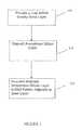
- the first stepincludes providing a seed layer on a substrate ( 105 in FIG. 1 ).
- 105refers to the label of the block in the flowchart of FIG. 1 .
- the seed layerhas the desired crystallographic orientation.
- Low defect density seed layersprovide good substrates from which to epitaxially grow a low defect density (epitaxial) thick film.
- large grained, crystallographically oriented Si filmscan be produced having a low defect density.
- Low defect density filmsare characterized by a low number of grain boundaries and few intergrain defects, e.g., significantly less than 10 9 defect/ ⁇ m 2 .
- the seed layercan be relatively thin, e.g., between about 50 and 1,000 nm or between about 100 and 200 nm.
- Zone melt irradiation using a radiative source of heatingcan produce silicon films having ⁇ 100 ⁇ surface orientation as described by M. W. Geis et. al., “Zone-Melting recrystallization of Si films with a moveable-strip-heater oven,” J. Electro-Chem. Soc. 129, 2812 (1982).
- textured films having a low number of grain boundariese.g., large crystalline grains, and a low defect density for use as a seed layer
- James ImU.S. Ser. No. 10/994,205, filed Nov. 18, 2004, and entitled “System and Methods for Creating Crystallographic Controlled Orientation Controlled PolySilicon Films,” the contents of which are incorporated herein in their entirety by reference.
- a filmwas pretreated to introduce a desired texture into the film and then crystallized using sequential lateral solidification (SLS) laser irradiation to form the enhanced grain growth that is typical of SLS.
- SLSsequential lateral solidification
- the process of pre-treating the filmis a mixed-phase solidification (MPS) process. This is a process that results in very low intragrain defect density in the crystalline structure.
- MPSmixed-phase solidification
- an amorphous or other low quality crystalline filmis deposited on the seed layer ( 110 in FIG. 1 ).
- 110refers to the label of the block in the flowchart of FIG. 1 .
- the filmis deposited using conventional methods, such as low pressure CVD, plasma enhanced CVD, physical deposition techniques such as sputter deposition, and the like.
- the amorphous layercan be many times thicker than the seed layer and can be, for example, about 1 ⁇ m to about 20 ⁇ m thick or about 2-6 ⁇ m thick or as high as 10-20 ⁇ m thick.
- the amorphous layercan be as thick as desired in the final product, for example, a solar panel.
- the high defect or top layerwill typically be thicker than the seed layer, it doesn't need to be thicker, e.g., the seed layer can be very thick ( ⁇ 1 ⁇ m) and it can be processed in multiple steps to provide a low defect density film.
- the seed layercan be very thick ( ⁇ 1 ⁇ m) and it can be processed in multiple steps to provide a low defect density film.
- 1 ⁇ m of the defective silicon layer, i.e., top layercan be deposited onto a seed layer followed by back side irradiation to induce epitaxy in the film.
- the seed layer and top layerare supported on a substrate that is transparent to laser energy over at least a portion of its area.
- transparent to laser energyit is meant that laser energy used in the treatment of the films described herein is not substantially absorbed by the substrate.
- laser energyis selectively absorbed by the film, with the concomitant heating and melting of at least a portion of the film. Irradiation from the back side of the substrate provides control over the extent of melting of the amorphous layer. Because the crystalline material of the seed layer melts at a higher temperature, it is possible to deposit enough energy to pass heat through the seed layer to induce melting of the defective layer without fully melting the seed layer.
- an initial region of the amorphous layer deposited above a crystalline seed layeris heated via radiation.
- the melting of the top layeris induced from the side of the a-Si that is in contact with the c-Si while the rest of the a-Si remains solid.
- the irradiationtypically occurs from the substrate side or back side of the film, as is shown in FIG. 2 .
- irradiationoccurs from the back side of the substrate so that only the region closest to the irradiation source and adjacent to the seed layer is melted.
- the lower melting point for the defective layercauses it to melt first, or at least to start melting, before too much of the crystalline seed layer is molten (i.e., the seed layer is nearly completely molten so that it becomes discontinuous), or even before it is fully molten.
- the radiationmay be absorbed by both layers, predominantly by the defective layer, or predominantly by the seed layer.
- the radiationmay be absorbed (predominantly) in the c-Si film, so that the a-Si layer is heated to melting (predominantly) through conduction.
- the first section of the amorphous layermelts and reforms as crystalline silicon
- an exothermis created by the energy being dissipated as heat from the silicon, as the silicon forms a more thermodynamically stable crystalline form.
- the amorphous materialmelts in the presence of the crystalline material, but the temperature of the liquid is still below the melting point of the crystalline material, the crystallizing materials will grow epitaxially from the seed layer. That exotherm is sufficient to melt adjacent amorphous silicon which itself then re-crystallizes as crystalline silicon and releases an additional amount of energy.
- An exothermtherefore, propagates as a wave through the material from the region closest to the substrate towards the upper surface.
- the explosive crystallization processwill continue until quenched or until all the amorphous material is transformed into crystalline material. Quenching is known to result in lowering of the temperature at the growth front and formation of defects and ultimately of halting of the process. Quenching is often the result of nearby conductive materials and/or nearby substrates. In the current configuration, however, significant quenching of the film is not to be expected because the fraction of the heat that is released at the growth front and that diffuses ‘upwards’ toward and into the remaining defective silicon is trapped therein. Also, the defective silicon typically has low thermal conductivity so that the heat does not quickly spread out over the film, but rather stays within the vicinity of the melting interface.
- the explosive crystallization processis expected to result in gradually smoothening of the melting and solidification interfaces.
- the explosive crystallization fronti.e., the closely spaced melting and solidification fronts
- the frontwill initially protrude into the defective layer as well and will therefore cool down more rapidly than elsewhere where the front may be planar or even curved negatively.
- the frontis expected to slow down with respect to other regions and the overall front is expected to flatten/smoothen.
- the laser source used to trigger the melting processcan be any pulsed or chopped laser source that emits light to which the substrate is substantially transparent but absorbable by the film stack.
- the lasermay be a CW laser or an excimer laser.
- light having a wavelength with an absorption depth on the order of or larger than the thickness of the precursor filmmay be used to promote heat absorption in the amorphous layer and reduce the heat absorbed in the seed layer. This can increase the process window in which a substantially continuous liquid film is created in the amorphous layer while a substantially continuous solid film remains in the crystalline precursor.
- Such wavelengthscan be, for example, around 500 nm or longer as emitted by, for example, a frequency-doubled Nd:YVO 4 or Nd:YAG laser (532 nm), or even longer wavelengths.
- the laser energy and pulse durationare sufficient to melt a portion of the amorphous layer adjacent to the seed layer, in some embodiments, in a single laser pulse.
- the laser pulsemelts a portion of the amorphous layer and induces explosive crystallization to transform a thick Si layer into a layer having crystalline properties in only a single laser pulse.
- the embodiments disclosed hereinpreferably use flood irradiation. Because of the beam used for flood irradiation, the edge region of the film can have a poorer quality as there will be lateral explosive crystallization there as well. The lateral part of the explosive front will quench more rapidly because of the two dimensional nature of the temperature profile. As such, there will be defect formation and defective growth. Upon overlapping with a second radiation pulse, this defective region, being already crystalline (albeit defectively), will not remelt. As such, a defective crystalline region with a short minority carrier lifetime will remain.
- a flood irradiation beam with sharp edges and a substantially uniform energy densityis used.
- Such a beamcan be obtained using SLS equipment or line-beam ELA equipment.
- the defective regionscan be positioned in areas where the film is later removed to create vias between the front contact of one cell and the back contact of the neighboring cell.
- the viascan be used to create cells in series.
- Some embodimentsuse flood irradiation with radiation areas as large as the panel (or a significant part thereof), for example, arrays of flash lamps or diode lasers.
- the long wavelengthis not sufficiently absorbed by the Si film, one can use metal layers under the seed layer and above the substrate, as discussed in more detail below. Further, these metal layers can be used to perform long wavelength flood irradiation from the top of the film.
- the filmcan melt completely upon backside radiation.
- Experimental workshows that for thin a-Si films (i.e., 200 nm on a 100 nm seed layer obtained via MPS), upon backside radiation, the a-Si was molten completely, while the seed layer remained at least partially intact. The texture reproduction was good with very little defect formation observed.
- a complete melting of the a-Sican be induced for a-Si films that are sufficiently thick for making a solar cell. This could be the case when longer wavelength radiation is used so that the absorption length exceeds the seed layer thickness.
- pre-heatingcan cause complete melting.
- top side radiation of moderately absorbed lightthat is mostly absorbed by a metal layer located between the seed layer and the substrate (and discussed in more detail below) can cause complete melting.
- the amount of energy used to irradiate the filmis less than that used in conventional melt-mediated epitaxy processes because only a thin region, and not the entire thick film, is melted. Therefore, a wider range of substrates can be used, including low temperature glasses and the like.
- the methods disclosed hereincan be used with, for example, glass substrates, but also with non-transparent substrates such as metal foils, such as stainless steel, or ceramic substrates.
- Heatingcan be accomplished by substrate pre-heating or co-irradiation from the front side. Heat can be introduced to the top layer, for example, by irradiation, furnace pre-heating, a hot plate, or any other conventional source. Heating can reduce the amount of energy needed for irradiation and reduce the exposure of the substrate to damaging levels of heat. It can also be used to modify or control the rate of liquid from propagation through the amorphous top layer. For example, heating the film can reduce crystallization velocity.
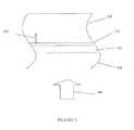
- FIG. 2is a schematic illustration of the back side irradiation and crystallization according to one or more embodiments of the disclosed subject matter.
- the film(only a portion of which is shown in the figure) includes a substrate 230 , on which is deposited a thin crystalline seed layer 220 and a thick amorphous silicon layer 200 .
- back side irradiationis described with respect to thin films in a co-pending application, filed on even date herewith, entitled “Systems and Methods for Preparing Epitaxially Textured Polycrystalline Films,” the entire disclosure of which is incorporated by reference.
- the method of back side irradiation of a thin filmincludes generating a textured precursor film and irradiating the film through the back side of the film, i.e., through the substrate to the film, to improve the texture throughout the film thickness.
- the back side irradiationcan be SLS irradiation, which can simultaneously create uniform texture and microstructure.
- the back side irradiationcan be flood irradiation. If a non-SLS back side irradiation method is implemented, the required microstructure can be created by front side, i.e., through the top surface of the crystalline film, SLS irradiation after the back side irradiation has been performed.
- the principals of back side irradiation of thin filmscan be applied to the thin films disclosed herein.
- the a-Si layer 200can be made by low pressure CVD.
- the filmthen is irradiated from the back side, as indicated by arrow 240 , resulting in the formation of a small amount of liquid silicon 210 at the interface between seed layer 220 and amorphous silicon 200 .
- the liquid phase 210crystallizes and propagates in an explosive process in a direction through the amorphous silicon layer 200 along arrow 250 .
- This irradiation methodologyhas the additional benefit of trapping the heat in the film.
- the heat that is released upwards of the filmgets trapped in a shrinking volume and thus temperature will rise.
- This temperature risewill result in a more gentle explosive crystallization taking place (e.g., crystallization velocity is decreased) and this will suppress the formation of defects.
- the crystallization velocitymay be further reduced by introducing additional heat, e.g., from the top surface of the film, as noted previously.
- a thin metal filmcan be deposited under the silicon seed layer.
- FIG. 3is a cross-sectional view of a thick film 300 including a substrate 302 , a metal film 304 , an optional buffer layer 306 , the seed layer 308 and the thick top layer 310 .
- the thin metal filmcan be composed of, for example, molybdenum.
- the buffer layercan be composed, for example, of silicon dioxide.
- the metallic absorptionoccurs in a metal substrate, such as a metal foil.
- no buffer layeris used and a metal layer is in direct contact with the a-Si film and can act as a backside contact in the solar cell stack.
- the silicon filmcan be irradiated from the top portion of the film, as shown in FIGS. 4 a - c .
- radiation 400irradiates the top portion of the top layer 310 and penetrates through the thickness of the film to the metal layer.
- the radiationis of a type such that the silicon in the top layer 310 and the seed layer 308 absorbs only a portion of the incoming light, while the majority of the light is absorbed by the thin metal film, shown at 405 .
- this absorptionheats the metal thin film 304 , thus providing heat to the silicon film from the bottom of the top layer adjacent to the seed layer and melting this portion of the top layer 410 .
- the light sourcecan be a laser, for example, a diode laser.
- the diode lasercan be an 808 nm laser.
Landscapes
- Engineering & Computer Science (AREA)
- Physics & Mathematics (AREA)
- Chemical & Material Sciences (AREA)
- Crystallography & Structural Chemistry (AREA)
- Condensed Matter Physics & Semiconductors (AREA)
- General Physics & Mathematics (AREA)
- Manufacturing & Machinery (AREA)
- Computer Hardware Design (AREA)
- Microelectronics & Electronic Packaging (AREA)
- Power Engineering (AREA)
- Materials Engineering (AREA)
- Metallurgy (AREA)
- Organic Chemistry (AREA)
- Optics & Photonics (AREA)
- Electromagnetism (AREA)
- Recrystallisation Techniques (AREA)
- Photovoltaic Devices (AREA)
Abstract
Description
This application is a continuation of and claims the benefit under 35 U.S.C. §120 of U.S. application Ser. No. 12/275,727, filed on Nov. 21, 2008, entitled “Systems and Methods for Preparation of Epitaxially Textured Thick Films,” now U.S. Pat. No. 8,557,040, the contents of which are incorporated herein by reference, which claims the benefit under 35 U.S.C. §119(e) of the following applications, the entire contents of which are incorporated herein by reference:
U.S. Provisional Application No. 60/989,729, filed on Nov. 21, 2007, entitled “Methods and Systems for Backside Laser Induced Epitaxial Growth of Thick Film”; and
U.S. Provisional Application No. 61/012,229, filed on Dec. 7, 2007, entitled “Methods and Systems for Backside Laser Induced Epitaxial Growth of Thick Film;” and
All patents, patent applications and patent publications cited herein are hereby incorporated by reference in their entirety.
This application is related to the commonly owned and co-pending application filed on even date herewith and entitled “Systems and Methods for Preparing Epitaxially Textured Polycrystalline Films,” the contents of which are incorporated by reference in their entirety.
The subject matter described herein relates to systems and methods for preparation of epitaxially grown textured thick films.
A thick film is particularly useful in solar cell applications because a thicker film can absorb more photons and thereby produce more electricity. A solar cell or photovoltaic cell is a device that converts light energy into electrical energy. A solar or photovoltaic cell generates electricity in a light absorbing material upon exposure of the material to light. When light energy strikes the solar cell, the photovoltaic effect produces electricity.
The light absorbing material is typically a semiconductor material. There are currently several different semiconducting materials used in solar cells and a common material is silicon. The most efficient form of silicon (e.g., to capture the greatest amount of energy from the incident light) is as a single crystal silicon. However, single-crystal silicon wafers are costly. In many photovoltaic applications, the silicon used is a relatively thick polycrystalline or amorphous silicon film. For example, a film having a thickness of about 1 μm to up to 20 μm can be used. Polycrystalline silicon or amorphous silicon can be used in an attempt to reduce manufacturing costs. However, the resulting cells are not as efficient as cells using single crystal silicon.
Silicon thin-films can be made through chemical vapor deposition (CVD) (for example plasma-enhanced (PE-CVD)) from, for example, silane gas and hydrogen gas. Depending on the deposition's parameters, this can yield amorphous silicon (a-Si) or polycrystalline silicon (poly-Si). The solar cells made from these materials tend to have lower energy conversion efficiency than bulk silicon, but are also less expensive to produce and they can be produced on large surfaces.
The disclosed subject matter relates to the use of laser crystallization of thin films to create epitaxially textured crystalline thick films.
In one or more embodiments, a method for preparing a thick crystalline film includes providing a film for crystallization on a substrate, wherein at least a portion of the substrate is substantially transparent to laser irradiation, said film including a seed layer having a predominant surface crystallographic orientation; and a top layer disposed above the seed layer; irradiating the film from the back side of the substrate using a pulsed laser to melt a first portion of the top layer at an interface with the seed layer while a second portion of the top layer remains solid; and re-solidifying the first portion of the top layer to form a crystalline laser epitaxial with the seed layer thereby releasing heat to melt an adjacent portion of the top layer.
In one or more embodiments, the seed layer includes a polycrystalline silicon.
In one or more embodiments, the top layer includes amorphous silicon.
In one or more embodiments, the top layer has a predominant surface crystallographic orientation of {111} orientation.
In one or more embodiments, the top layer has a predominant surface crystallographic orientation of {100} orientation.
In one or more embodiments, the top layer has a thickness that is greater than the seed layer.
In one or more embodiments, the seed layer is deposited using a technique selected from the group consisting of zone melt recrystallization (ZMR), solid phase recrystallization, chemical vapor deposition (CVD), sputtering, evaporation, surface-energy-driven secondary grain growth (SEDSGG), mixed-phase solidification and pulsed laser crystallization methods.
In one or more embodiments, the method includes backside irradiating the seed layer using pulsed irradiation to increase the texture of the seed layer through the thickness of the seed layer.
In one or more embodiments, the top layer is deposited using a method selected from the group consisting of low pressure chemical vapor deposition (CVD), plasma enhanced CVD, physical deposition techniques and sputter deposition.
In one or more embodiments, the film includes a material selected from the group consisting of metal and semiconductor materials.
In one or more embodiments, the top layer has a thickness in the range of 1 μm to about 20 μm.
In one or more embodiments, the seed layer has a thickness in the range of 50 nm to about 1 μm.
In one or more embodiments, the step of irradiating the film includes irradiating with a continuous wave or excimer laser.
In one or more embodiments, the method includes heating the film from the top surface of the film.
In one or more embodiments, heating includes co-irradiation from front side of film.
In one or more embodiments, heating includes contact with heated surface.
In one or more embodiments, the irradiation melts the entire top layer.
In one or more embodiments, a method for preparing a thick crystalline film includes providing a film for crystallization on a substrate, wherein at least a portion of the substrate is transparent to laser irradiation, said film including a seed layer having predominant surface crystallographic orientation; a top layer disposed above the seed layer; and a metal layer disposed below the seed layer; irradiating the film using a pulsed laser at a wavelength absorbable by the metal to heat the metal layer, said heat being transferred to the top layer to melt a first portion of the top layer at an interface with the seed layer while a second portion of the top layer remains solid; re-solidifying the first portion of the top layer to form a crystalline layer epitaxial with the seed layer thereby releasing heat to melt an adjacent portion of the top layer.
In one or more embodiments, the step of irradiating is directed through the front side of the film.
In one or more embodiments, a portion of the light is absorbed by the film.
In one or more embodiments, the step of irradiating is directed through the back side of the film.
In one or more embodiments, the method includes providing a buffer layer between the seed layer and the metal film.
In one or more embodiments, a method of making a solar cell including preparing a crystalline silicon layer by providing a film for crystallization on a substrate, wherein at least a portion of the substrate is transparent to laser irradiation, said film including a seed layer including crystal grains having a surface texture; and a top layer disposed above the low defect density seed layer, said top layer having a thickness that is greater than the seed layer; irradiating the film from the back side of the substrate using a pulsed laser to melt a portion of the low quality layer at an interface with the seed layer, wherein crystals grow epitaxially from the seed layer; and disposing the polycrystalline silicon layer between two electrodes.
In one or more embodiments, the top layer has a thickness that is greater than the seed layer.
In one or more embodiments, a system for preparing a thick crystalline film includes a substrate, wherein at least a portion of the substrate is transparent to laser irradiation, said film including a film for crystallization disposed upon the substrate, the film including a seed layer including crystal grains having a surface texture; and a top layer disposed above the seed layer; means for irradiating the film from the back side of the substrate using a pulsed laser to melt a first portion of the top layer at an interface with the seed layer while a second portion of the top layer remains solid; and means for growing the first portion of a crystalline material to form an epitaxial layer on the seed layer, thereby releasing heat sufficient to melt an adjacent portion of the top layer.
In one or more embodiments, the top layer has a thickness that is greater than the seed layer.
The foregoing and other features of the embodiments described herein will be apparent from the following more particular description, as illustrated in the accompanying drawings.
Conventionally, the epitaxial growth of thin films is conducted using a chemical vapor deposition (CVD) process performed at high temperatures to ensure high quality reproduction of the seed layer's lattice orientation. However, such processes require the use of substrates that can withstand high temperatures. If transparency of the substrate is also required or desired, as may be the case for solar cells, the substrate needs to be made of quartz or specialized high-temperature glasses. These substrates can be costly and may not be available in large dimensions. In addition, epitaxy via CVD typically may have very low deposition rates.
Previously, epitaxial films have been prepared by depositing a thick defective layer, also referred to herein as a “top layer” (e.g., an amorphous silicon (a-Si) layer or polycrystalline silicon films (p-Si)) on a thin crystalline seed layer (c-Si) and melting the a-Si layer to provide an epitaxially grown layer from the crystalline seed layer using melt-mediated epitaxy. To epitaxially grow the silicon layer, the film is irradiated from the front side, i.e., the non-substrate side of the film, to melt completely the a-Si layer without substantially melting the underlying c-Si layer. Thus, the crystalline layer grows from the interface of the liquid-solid interface between the seed layer and the melt. However, this process can be difficult to control. Because the desired thickness of the a-Si layer is typically greater than that of the seed layer, it is difficult to melt only the deposited a-Si layer. This difficulty can arise from non-uniformities in the irradiation process including pulse-to-pulse energy variation. Significant care is required to avoid undesired melting of the seed layer along with the a-Si layer. Furthermore, the melt and grow process may need to be carried out multiple times. Typically, the thickness of the a-Si layer can range from 20 nm to 80 nm or more, e.g. 500 nm. Since the films are deposited on crystalline Si seed layers that are conductive to heat, higher energy density radiation may be needed to fully melt the film than if it were deposited on less conductive substrates, such as silicon dioxide. The high energy density that is required to deposit sufficient heat to completely melt the defective film can lead to damaging of the surface, for example through evaporation or through agglomeration. This limits the maximum thickness of the defective layer that can be fully molten without inducing damage. This is yet another reason why multiple depositions and radiations may be needed to reach satisfactory thickness of the photon absorption layer. Thin film solar cells typically have silicon layers on the order of about 1 μm to about 20 μm or more. Thus, many iterations of a-Si deposition and liquid phase epitaxial growth are required to obtain the desired thickness. This process can be time-consuming, costly, and inefficient.
The laser-irradiation epitaxial process, as described herein, provides good quality epitaxy and is compatible with low temperature substrates such as low temperature glass. The method includes inducing a limited degree of melting in the film and triggering a self-sustained process known as explosive crystallization. Explosive crystallization can take place as a result of the difference in melting temperatures of amorphous and crystalline materials. Amorphous silicon has a lower melting temperature than crystalline silicon (Ta-Si<Tc-Si), which helps to inhibit the melting of the seed crystalline layer and to promote the preferential melting of the amorphous silicon layer. Further, amorphous silicon is in a meta-stable state and has a higher free energy. Conversion of a meta-stable material such as amorphous silicon into a more stable material such as crystalline silicon (as a result of melt irradiation, followed by crystallization) results in a net reduction of energy, and therefore releases latent energy upon crystallization. In a crystallization process, this can translate into heat. Since crystallization of the amorphous materials results in the release of energy, it is possible to use the released energy to melt adjacent amorphous regions and to cause further crystallization. In many instances, the crystallization process can be self-sustaining and only need be initiated for crystallization to propagate through the amorphous body.
Aspects of the method are described with reference toFIG. 1 . For clarity of explanation, the method is described with reference to silicon films. However, it is apparent that the method can be applied to other materials. For example, the film can be a metal alloy or semiconductor film. Metal alloys can include nickel titanium. Semiconductor films can include conventional semiconductor materials, such as silicon, germanium, and silicon-germanium. In some embodiments, the defective material is a-Si.
The first step includes providing a seed layer on a substrate (105 inFIG. 1 ). In this example,105 refers to the label of the block in the flowchart ofFIG. 1 . The seed layer has the desired crystallographic orientation.
Low defect density seed layers provide good substrates from which to epitaxially grow a low defect density (epitaxial) thick film. Thus, large grained, crystallographically oriented Si films can be produced having a low defect density. Low defect density films are characterized by a low number of grain boundaries and few intergrain defects, e.g., significantly less than 109defect/μm2. The seed layer can be relatively thin, e.g., between about 50 and 1,000 nm or between about 100 and 200 nm.
Conventional methods of obtaining a precursor textured film (which can be subsequently treated to form a large crystalline grain film) include zone melt recrystallization (ZMR), solid phase crystallization, direct deposition techniques (CVD, sputtering, evaporation), surface-energy-driven secondary grain growth (SEDSGG) and pulsed laser crystallization (multiple-pulse ELA) methods. Zone melt irradiation using a radiative source of heating can produce silicon films having {100} surface orientation as described by M. W. Geis et. al., “Zone-Melting recrystallization of Si films with a moveable-strip-heater oven,” J. Electro-Chem. Soc. 129, 2812 (1982). Other methods for producing (100) textured films include CVD and low-pressure CVD. See, e.g.,J. Electrochem. Soc. Vol. 134, NO. 134, pp. 2541-2545 (October, 1987);J. Appl. Phys., Vol. 73, No. 12, pp. 8402-8411 (June, 1993); andJ. Matl. Sci. Lett., Vol. 7, pp. 247-250 (1988), or by aluminum induced crystallization; see e.g., O. Nast, Appl. Phys. Lett. 73, No 22, pp. 3214-6 (November 1998). It is envisioned that other texture-inducing methods can also be used in a similar way to generate the textured precursors.
The formation of textured films having a low number of grain boundaries, e.g., large crystalline grains, and a low defect density for use as a seed layer, has been previously described in an application by James Im, U.S. Ser. No. 10/994,205, filed Nov. 18, 2004, and entitled “System and Methods for Creating Crystallographic Controlled Orientation Controlled PolySilicon Films,” the contents of which are incorporated herein in their entirety by reference. In that process, a film was pretreated to introduce a desired texture into the film and then crystallized using sequential lateral solidification (SLS) laser irradiation to form the enhanced grain growth that is typical of SLS. U.S. Pat. No. 6,322,625, entitled “Method and Tool for Generating Countersunk Holes in Composite Materials,” as filed Nov. 18, 1981; U.S. Pat. No. 6,368,945, entitled “Method and System for Providing a Continuous Motion Sequential Lateral Solidification,” as filed Mar. 16, 2000; U.S. Pat. No. 6,555,449, entitled “Methods for Producing Uniform Large-Grained and Grain Boundary Location Manipulated Polycrystalline Thin Film Semiconductors Using Sequential Lateral Solidification,” as filed Sep. 3, 1999; U.S. Pat. No. 6,573,531, entitled “Systems and Methods Using Sequential Lateral Solidification for Producing Single or Polycrystalline Silicon Thin Films at Low Temperatures,” as filed Sep. 3, 1999; and U.S. Provisional Patent Application No. 61/111,518, entitled “Flash Light Annealing for Thin Films,” as filed on Nov. 5, 2008, issued to Dr. James Im, the entire disclosures of which are incorporated herein by reference, and which are assigned to the common assignee of the present application, describe such SLS systems and processes. In one or more embodiments, the process of pre-treating the film is a mixed-phase solidification (MPS) process. This is a process that results in very low intragrain defect density in the crystalline structure.
Once the seed layer having the desired intragrain defect density and density of grain boundaries is provided, an amorphous or other low quality crystalline film is deposited on the seed layer (110 inFIG. 1 ). In this example,110 refers to the label of the block in the flowchart ofFIG. 1 . The film is deposited using conventional methods, such as low pressure CVD, plasma enhanced CVD, physical deposition techniques such as sputter deposition, and the like.
The amorphous layer can be many times thicker than the seed layer and can be, for example, about 1 μm to about 20 μm thick or about 2-6 μm thick or as high as 10-20 μm thick. The amorphous layer can be as thick as desired in the final product, for example, a solar panel.
Although the high defect or top layer will typically be thicker than the seed layer, it doesn't need to be thicker, e.g., the seed layer can be very thick (˜1 μm) and it can be processed in multiple steps to provide a low defect density film. For example, 1 μm of the defective silicon layer, i.e., top layer, can be deposited onto a seed layer followed by back side irradiation to induce epitaxy in the film.
The seed layer and top layer are supported on a substrate that is transparent to laser energy over at least a portion of its area. By “transparent to laser energy,” it is meant that laser energy used in the treatment of the films described herein is not substantially absorbed by the substrate. Thus, laser energy is selectively absorbed by the film, with the concomitant heating and melting of at least a portion of the film. Irradiation from the back side of the substrate provides control over the extent of melting of the amorphous layer. Because the crystalline material of the seed layer melts at a higher temperature, it is possible to deposit enough energy to pass heat through the seed layer to induce melting of the defective layer without fully melting the seed layer.
According to the embodiments disclosed herein, an initial region of the amorphous layer deposited above a crystalline seed layer is heated via radiation. The melting of the top layer is induced from the side of the a-Si that is in contact with the c-Si while the rest of the a-Si remains solid. As the seed layer is typically deposited or grown directly on the substrate, the irradiation typically occurs from the substrate side or back side of the film, as is shown inFIG. 2 . Thus, as shown at110 inFIG. 1 , irradiation occurs from the back side of the substrate so that only the region closest to the irradiation source and adjacent to the seed layer is melted. While both the seed layer and the defective thick film are irradiated, the lower melting point for the defective layer causes it to melt first, or at least to start melting, before too much of the crystalline seed layer is molten (i.e., the seed layer is nearly completely molten so that it becomes discontinuous), or even before it is fully molten. The radiation may be absorbed by both layers, predominantly by the defective layer, or predominantly by the seed layer. The radiation may be absorbed (predominantly) in the c-Si film, so that the a-Si layer is heated to melting (predominantly) through conduction. As the first section of the amorphous layer melts and reforms as crystalline silicon, an exotherm is created by the energy being dissipated as heat from the silicon, as the silicon forms a more thermodynamically stable crystalline form. As the amorphous material melts in the presence of the crystalline material, but the temperature of the liquid is still below the melting point of the crystalline material, the crystallizing materials will grow epitaxially from the seed layer. That exotherm is sufficient to melt adjacent amorphous silicon which itself then re-crystallizes as crystalline silicon and releases an additional amount of energy. An exotherm, therefore, propagates as a wave through the material from the region closest to the substrate towards the upper surface.
Generally, the explosive crystallization process will continue until quenched or until all the amorphous material is transformed into crystalline material. Quenching is known to result in lowering of the temperature at the growth front and formation of defects and ultimately of halting of the process. Quenching is often the result of nearby conductive materials and/or nearby substrates. In the current configuration, however, significant quenching of the film is not to be expected because the fraction of the heat that is released at the growth front and that diffuses ‘upwards’ toward and into the remaining defective silicon is trapped therein. Also, the defective silicon typically has low thermal conductivity so that the heat does not quickly spread out over the film, but rather stays within the vicinity of the melting interface.
While the initial interface between the seed layer and the defective top layer may be rough, as, for example, with films obtained via MPS, the explosive crystallization process is expected to result in gradually smoothening of the melting and solidification interfaces. For those regions where the seed layer is protruding into the defective layer, the explosive crystallization front (i.e., the closely spaced melting and solidification fronts) will initially protrude into the defective layer as well and will therefore cool down more rapidly than elsewhere where the front may be planar or even curved negatively. As a result, the front is expected to slow down with respect to other regions and the overall front is expected to flatten/smoothen.
The laser source used to trigger the melting process can be any pulsed or chopped laser source that emits light to which the substrate is substantially transparent but absorbable by the film stack. For example, the laser may be a CW laser or an excimer laser. Additionally, light having a wavelength with an absorption depth on the order of or larger than the thickness of the precursor film may be used to promote heat absorption in the amorphous layer and reduce the heat absorbed in the seed layer. This can increase the process window in which a substantially continuous liquid film is created in the amorphous layer while a substantially continuous solid film remains in the crystalline precursor. Such wavelengths can be, for example, around 500 nm or longer as emitted by, for example, a frequency-doubled Nd:YVO4or Nd:YAG laser (532 nm), or even longer wavelengths. The laser energy and pulse duration are sufficient to melt a portion of the amorphous layer adjacent to the seed layer, in some embodiments, in a single laser pulse.
In one or more embodiments, the laser pulse melts a portion of the amorphous layer and induces explosive crystallization to transform a thick Si layer into a layer having crystalline properties in only a single laser pulse. The embodiments disclosed herein preferably use flood irradiation. Because of the beam used for flood irradiation, the edge region of the film can have a poorer quality as there will be lateral explosive crystallization there as well. The lateral part of the explosive front will quench more rapidly because of the two dimensional nature of the temperature profile. As such, there will be defect formation and defective growth. Upon overlapping with a second radiation pulse, this defective region, being already crystalline (albeit defectively), will not remelt. As such, a defective crystalline region with a short minority carrier lifetime will remain.
To alleviate some of these concerns, a flood irradiation beam with sharp edges and a substantially uniform energy density is used. Such a beam can be obtained using SLS equipment or line-beam ELA equipment. For those embodiments where the pulse is smaller than the area of the film, the defective regions can be positioned in areas where the film is later removed to create vias between the front contact of one cell and the back contact of the neighboring cell. The vias can be used to create cells in series. Some embodiments use flood irradiation with radiation areas as large as the panel (or a significant part thereof), for example, arrays of flash lamps or diode lasers. When the long wavelength is not sufficiently absorbed by the Si film, one can use metal layers under the seed layer and above the substrate, as discussed in more detail below. Further, these metal layers can be used to perform long wavelength flood irradiation from the top of the film.
In some embodiments, the film can melt completely upon backside radiation. Experimental work shows that for thin a-Si films (i.e., 200 nm on a 100 nm seed layer obtained via MPS), upon backside radiation, the a-Si was molten completely, while the seed layer remained at least partially intact. The texture reproduction was good with very little defect formation observed. A complete melting of the a-Si can be induced for a-Si films that are sufficiently thick for making a solar cell. This could be the case when longer wavelength radiation is used so that the absorption length exceeds the seed layer thickness. Also, pre-heating can cause complete melting. Furthermore, top side radiation of moderately absorbed light that is mostly absorbed by a metal layer located between the seed layer and the substrate (and discussed in more detail below) can cause complete melting.
As is discussed above, the amount of energy used to irradiate the film is less than that used in conventional melt-mediated epitaxy processes because only a thin region, and not the entire thick film, is melted. Therefore, a wider range of substrates can be used, including low temperature glasses and the like. For example, the methods disclosed herein can be used with, for example, glass substrates, but also with non-transparent substrates such as metal foils, such as stainless steel, or ceramic substrates.
In other embodiments, additional heat is added to sustain the process. Heating can be accomplished by substrate pre-heating or co-irradiation from the front side. Heat can be introduced to the top layer, for example, by irradiation, furnace pre-heating, a hot plate, or any other conventional source. Heating can reduce the amount of energy needed for irradiation and reduce the exposure of the substrate to damaging levels of heat. It can also be used to modify or control the rate of liquid from propagation through the amorphous top layer. For example, heating the film can reduce crystallization velocity.
This irradiation methodology has the additional benefit of trapping the heat in the film. As crystallization proceeds upwards in the film, the heat that is released upwards of the film gets trapped in a shrinking volume and thus temperature will rise. This temperature rise will result in a more gentle explosive crystallization taking place (e.g., crystallization velocity is decreased) and this will suppress the formation of defects. The crystallization velocity may be further reduced by introducing additional heat, e.g., from the top surface of the film, as noted previously.
In some embodiments, a thin metal film can be deposited under the silicon seed layer.FIG. 3 is a cross-sectional view of athick film 300 including asubstrate 302, ametal film 304, anoptional buffer layer 306, theseed layer 308 and the thicktop layer 310. The thin metal film can be composed of, for example, molybdenum. The buffer layer can be composed, for example, of silicon dioxide. In some embodiments, the metallic absorption occurs in a metal substrate, such as a metal foil. In some embodiments, no buffer layer is used and a metal layer is in direct contact with the a-Si film and can act as a backside contact in the solar cell stack.
In embodiments having the thin metal film layer, the silicon film can be irradiated from the top portion of the film, as shown inFIGS. 4 a-c. InFIG. 4 a,radiation 400 irradiates the top portion of thetop layer 310 and penetrates through the thickness of the film to the metal layer. The radiation is of a type such that the silicon in thetop layer 310 and theseed layer 308 absorbs only a portion of the incoming light, while the majority of the light is absorbed by the thin metal film, shown at405. As shown inFIG. 4 b, this absorption heats the metalthin film 304, thus providing heat to the silicon film from the bottom of the top layer adjacent to the seed layer and melting this portion of thetop layer 410. As discussed earlier, the steps of heating and melting propagate throughout the top layer through explosive crystallization, as shown in FIG.4c, where the previously meltedlayer 420 is crystallizing and heating a next portion of thetop layer 420. Thus, this method provides similar heating to the silicon film as the back side radiation embodiment. The light source can be a laser, for example, a diode laser. For example, the diode laser can be an 808 nm laser.
While there have been shown and described examples of the disclosed subject matter, it will be readily apparent to those skilled in the art that various changes and modifications may be readily apparent to those skilled in the art that various changes and modifications may be made therein without departing from the scope of the disclosed subject matter as defined by the appended claims. Accordingly, the disclosed subject matter is limited only by the following claims and equivalents thereto.
Claims (21)
1. A system for preparing a thick crystalline film comprising:
a substrate, wherein at least a portion of the substrate is transparent to laser irradiation;
a film for crystallization disposed upon the substrate, the film comprising:
(a) a seed layer having a predominant surface crystallographic orientation; and
(b) a top layer disposed above the seed layer;
a heat source to heat the film from the top surface of the film; and
a pulsed laser for irradiating the film from the back side of the substrate to melt a first portion of the top layer at an interface with the seed layer while a second portion of the top layer remains solid,
wherein upon irradiation and cooling, the first portion of the top layer material forms a crystalline layer epitaxial with the seed layer, thereby releasing heat sufficient to melt an adjacent portion of the top layer.
2. The system ofclaim 1 , wherein the heat source co-irradiates from the front side of the film.
3. The system ofclaim 1 , wherein the film comprises a metal layer disposed below the seed layer.
4. The system ofclaim 1 , wherein the seed layer comprises polycrystalline silicon.
5. The system ofclaim 1 , wherein the seed layer comprises amorphous silicon.
6. The system ofclaim 1 , wherein the heat source comprises a heated surface.
7. The system ofclaim 1 , wherein the top layer has a thickness that is greater than the seed layer.
8. The system ofclaim 1 , wherein the pulsed laser comprises a continuous wave or excimer laser.
9. The system ofclaim 1 , wherein the top layer has a thickness in the range of about 1 micron to about 20 microns.
10. The system ofclaim 1 , wherein the seed layer has a thickness in the range of about 50 nm to about 1 microns.
11. A system for preparing a thick crystalline film comprising:
a substrate, wherein at least a portion of the substrate is transparent to laser irradiation;
a film for crystallization disposed upon the substrate, the film comprising:
(a) a seed layer having a predominant surface crystallographic orientation;
(b) a top layer disposed above the seed layer; and
(c) a metal layer disposed below the seed layer; and
a pulsed laser having a wavelength absorbable by the metal to irradiate and heat the metal layer, said heat being transferred to the top layer to melt a first portion of the top layer at an interface with the seed layer while a second portion of the top layer remains solid,
wherein upon irradiation and cooling, the first portion of the top layer material forms a crystalline layer epitaxial layer with the seed layer, thereby releasing heat sufficient to melt an adjacent portion of the top layer.
12. The system ofclaim 11 , wherein the laser irradiation is directed through the front side of the film.
13. The system ofclaim 11 , where a portion of the laser irradiation is absorbed by the film.
14. The system ofclaim 11 , wherein the laser irradiation is directed through the back side of the substrate.
15. The system ofclaim 11 , further comprising a buffer layer between the seed layer and the metal film.
16. The system ofclaim 11 , wherein the top layer has a thickness in the range of about 1 micron to about 20 microns.
17. The system ofclaim 11 , wherein the seed layer has a thickness in the range of about 50 nm to about 1 microns.
18. The system ofclaim 11 , wherein the top layer has a thickness that is greater than the seed layer.
19. The system ofclaim 11 , wherein the pulsed laser comprises a continuous wave or excimer laser.
20. The system ofclaim 11 , wherein the seed layer comprises polycrystalline silicon.
21. The system ofclaim 11 , wherein the seed layer comprises amorphous silicon.
Priority Applications (1)
| Application Number | Priority Date | Filing Date | Title |
|---|---|---|---|
| US14/053,349US8871022B2 (en) | 2007-11-21 | 2013-10-14 | Systems and methods for preparation of epitaxially textured thick films |
Applications Claiming Priority (4)
| Application Number | Priority Date | Filing Date | Title |
|---|---|---|---|
| US98972907P | 2007-11-21 | 2007-11-21 | |
| US1222907P | 2007-12-07 | 2007-12-07 | |
| US12/275,727US8557040B2 (en) | 2007-11-21 | 2008-11-21 | Systems and methods for preparation of epitaxially textured thick films |
| US14/053,349US8871022B2 (en) | 2007-11-21 | 2013-10-14 | Systems and methods for preparation of epitaxially textured thick films |
Related Parent Applications (1)
| Application Number | Title | Priority Date | Filing Date |
|---|---|---|---|
| US12/275,727ContinuationUS8557040B2 (en) | 2007-11-21 | 2008-11-21 | Systems and methods for preparation of epitaxially textured thick films |
Publications (2)
| Publication Number | Publication Date |
|---|---|
| US20140045346A1 US20140045346A1 (en) | 2014-02-13 |
| US8871022B2true US8871022B2 (en) | 2014-10-28 |
Family
ID=40642397
Family Applications (2)
| Application Number | Title | Priority Date | Filing Date |
|---|---|---|---|
| US12/275,727Expired - Fee RelatedUS8557040B2 (en) | 2007-11-21 | 2008-11-21 | Systems and methods for preparation of epitaxially textured thick films |
| US14/053,349Expired - Fee RelatedUS8871022B2 (en) | 2007-11-21 | 2013-10-14 | Systems and methods for preparation of epitaxially textured thick films |
Family Applications Before (1)
| Application Number | Title | Priority Date | Filing Date |
|---|---|---|---|
| US12/275,727Expired - Fee RelatedUS8557040B2 (en) | 2007-11-21 | 2008-11-21 | Systems and methods for preparation of epitaxially textured thick films |
Country Status (6)
| Country | Link |
|---|---|
| US (2) | US8557040B2 (en) |
| EP (1) | EP2212913A4 (en) |
| JP (1) | JP5443377B2 (en) |
| KR (1) | KR20100105606A (en) |
| CN (2) | CN103354204A (en) |
| WO (1) | WO2009067687A1 (en) |
Families Citing this family (16)
| Publication number | Priority date | Publication date | Assignee | Title |
|---|---|---|---|---|
| WO2009067687A1 (en)* | 2007-11-21 | 2009-05-28 | The Trustees Of Columbia University In The City Of New York | Systems and methods for preparation of epitaxially textured thick films |
| WO2011017179A2 (en)* | 2009-07-28 | 2011-02-10 | Gigasi Solar, Inc. | Systems, methods and materials including crystallization of substrates via sub-melt laser anneal, as well as products produced by such processes |
| US8440581B2 (en) | 2009-11-24 | 2013-05-14 | The Trustees Of Columbia University In The City Of New York | Systems and methods for non-periodic pulse sequential lateral solidification |
| US9087696B2 (en) | 2009-11-03 | 2015-07-21 | The Trustees Of Columbia University In The City Of New York | Systems and methods for non-periodic pulse partial melt film processing |
| US9646831B2 (en) | 2009-11-03 | 2017-05-09 | The Trustees Of Columbia University In The City Of New York | Advanced excimer laser annealing for thin films |
| WO2011056787A1 (en)* | 2009-11-03 | 2011-05-12 | The Trustees Of Columbia University In The City Of New York | Systems and methods for non-periodic pulse partial melt film processing |
| KR101117265B1 (en)* | 2010-01-13 | 2012-03-20 | 삼성코닝정밀소재 주식회사 | Substrate of photovoltaic cell and method for manufacturing the same |
| WO2012012806A2 (en)* | 2010-07-23 | 2012-01-26 | Gigasi Solar, Inc. | Thin film solar cells and other devices, systems and methods of fabricating same, and products produced by processes thereof |
| CN102386072B (en)* | 2010-08-25 | 2016-05-04 | 株式会社半导体能源研究所 | The manufacture method of microcrystalline semiconductor film and the manufacture method of semiconductor device |
| DE102010044480A1 (en)* | 2010-09-03 | 2012-03-08 | Institut Für Photonische Technologien E.V. | Method and device for producing a thin-film solar cell |
| DE102012004314A1 (en)* | 2012-02-29 | 2013-08-29 | Helmholtz-Zentrum Berlin Für Materialien Und Energie Gmbh | Method for producing a thin Si absorber layer, thin-film silicon absorber and its use |
| US9543457B2 (en)* | 2012-09-28 | 2017-01-10 | First Solar, Inc. | Method and system for manufacturing back contacts of photovoltaic devices |
| GB2566477A (en)* | 2017-09-14 | 2019-03-20 | Nat Univ Ireland Galway | Method of processing a target material |
| JP7317482B2 (en)* | 2018-10-16 | 2023-07-31 | 株式会社ディスコ | Wafer processing method |
| KR102604059B1 (en)* | 2020-12-18 | 2023-11-17 | 삼성전자주식회사 | Manufacturing method of semiconductor device |
| CN114784148B (en) | 2022-06-15 | 2022-09-23 | 浙江晶科能源有限公司 | Preparation method of solar cell, solar cell and photovoltaic module |
Citations (281)
| Publication number | Priority date | Publication date | Assignee | Title |
|---|---|---|---|---|
| US3632205A (en) | 1969-01-29 | 1972-01-04 | Thomson Csf | Electro-optical image-tracing systems, particularly for use with laser beams |
| US4234358A (en) | 1979-04-05 | 1980-11-18 | Western Electric Company, Inc. | Patterned epitaxial regrowth using overlapping pulsed irradiation |
| US4309225A (en) | 1979-09-13 | 1982-01-05 | Massachusetts Institute Of Technology | Method of crystallizing amorphous material with a moving energy beam |
| JPS5727035Y1 (en) | 1972-09-08 | 1982-06-11 | ||
| US4382658A (en) | 1980-11-24 | 1983-05-10 | Hughes Aircraft Company | Use of polysilicon for smoothing of liquid crystal MOS displays |
| US4456371A (en) | 1982-06-30 | 1984-06-26 | International Business Machines Corporation | Optical projection printing threshold leveling arrangement |
| US4639277A (en) | 1984-07-02 | 1987-01-27 | Eastman Kodak Company | Semiconductor material on a substrate, said substrate comprising, in order, a layer of organic polymer, a layer of metal or metal alloy and a layer of dielectric material |
| US4653903A (en) | 1984-01-24 | 1987-03-31 | Canon Kabushiki Kaisha | Exposure apparatus |
| JPS62181419A (en) | 1986-02-05 | 1987-08-08 | Nec Corp | Recrystallization method of polycrystalline silicon |
| US4691983A (en) | 1983-10-14 | 1987-09-08 | Hitachi, Ltd. | Optical waveguide and method for making the same |
| JPS62216320A (en) | 1986-03-18 | 1987-09-22 | Fujitsu Ltd | Laser annealing equipment |
| JPS62160781U (en) | 1986-04-01 | 1987-10-13 | ||
| US4727047A (en) | 1980-04-10 | 1988-02-23 | Massachusetts Institute Of Technology | Method of producing sheets of crystalline material |
| US4758533A (en) | 1987-09-22 | 1988-07-19 | Xmr Inc. | Laser planarization of nonrefractory metal during integrated circuit fabrication |
| US4793694A (en) | 1986-04-23 | 1988-12-27 | Quantronix Corporation | Method and apparatus for laser beam homogenization |
| US4800179A (en) | 1986-06-13 | 1989-01-24 | Fujitsu Limited | Method for fabricating semiconductor device |
| US4855014A (en) | 1986-01-24 | 1989-08-08 | Sharp Kabushiki Kaisha | Method for manufacturing semiconductor devices |
| US4870031A (en) | 1985-10-07 | 1989-09-26 | Kozo Iizuka, Director General, Agency Of Industrial Science And Technology | Method of manufacturing a semiconductor device |
| JPH01256114A (en) | 1988-04-06 | 1989-10-12 | Hitachi Ltd | Laser annealing method |
| US4940505A (en) | 1988-12-02 | 1990-07-10 | Eaton Corporation | Method for growing single crystalline silicon with intermediate bonding agent and combined thermal and photolytic activation |
| US4970546A (en) | 1988-04-07 | 1990-11-13 | Nikon Corporation | Exposure control device |
| US4977104A (en) | 1988-06-01 | 1990-12-11 | Matsushita Electric Industrial Co., Ltd. | Method for producing a semiconductor device by filling hollows with thermally decomposed doped and undoped polysilicon |
| US5032233A (en) | 1990-09-05 | 1991-07-16 | Micron Technology, Inc. | Method for improving step coverage of a metallization layer on an integrated circuit by use of a high melting point metal as an anti-reflective coating during laser planarization |
| US5061655A (en) | 1990-02-16 | 1991-10-29 | Mitsubishi Denki Kabushiki Kaisha | Method of producing SOI structures |
| US5076667A (en) | 1990-01-29 | 1991-12-31 | David Sarnoff Research Center, Inc. | High speed signal and power supply bussing for liquid crystal displays |
| JPH0433327A (en) | 1990-05-30 | 1992-02-04 | Kyocera Corp | Method for forming semiconductor crystallized film |
| USRE33836E (en) | 1987-10-22 | 1992-03-03 | Mrs Technology, Inc. | Apparatus and method for making large area electronic devices, such as flat panel displays and the like, using correlated, aligned dual optical systems |
| US5145808A (en) | 1990-08-22 | 1992-09-08 | Sony Corporation | Method of crystallizing a semiconductor thin film |
| JPH04279064A (en) | 1991-03-07 | 1992-10-05 | Sharp Corp | Display device |
| US5173441A (en) | 1991-02-08 | 1992-12-22 | Micron Technology, Inc. | Laser ablation deposition process for semiconductor manufacture |
| US5204659A (en) | 1987-11-13 | 1993-04-20 | Honeywell Inc. | Apparatus and method for providing a gray scale in liquid crystal flat panel displays |
| US5233207A (en) | 1990-06-25 | 1993-08-03 | Nippon Steel Corporation | MOS semiconductor device formed on insulator |
| US5247375A (en) | 1990-03-09 | 1993-09-21 | Hitachi, Ltd. | Display device, manufacturing method thereof and display panel |
| US5281840A (en) | 1991-03-28 | 1994-01-25 | Honeywell Inc. | High mobility integrated drivers for active matrix displays |
| US5285236A (en) | 1992-09-30 | 1994-02-08 | Kanti Jain | Large-area, high-throughput, high-resolution projection imaging system |
| US5291240A (en) | 1992-10-27 | 1994-03-01 | Anvik Corporation | Nonlinearity-compensated large-area patterning system |
| US5294811A (en) | 1990-11-30 | 1994-03-15 | Hitachi, Ltd. | Thin film semiconductor device having inverted stagger structure, and device having such semiconductor device |
| JPH0611729Y2 (en) | 1986-03-28 | 1994-03-30 | 大和工業株式会社 | Movable location pin device |
| US5304357A (en) | 1991-05-15 | 1994-04-19 | Ricoh Co. Ltd. | Apparatus for zone melting recrystallization of thin semiconductor film |
| US5338959A (en) | 1992-03-30 | 1994-08-16 | Samsung Electronics Co., Ltd. | Thin film transistor with three dimensional multichannel structure |
| JPH06260502A (en) | 1993-03-04 | 1994-09-16 | Seiko Epson Corp | Manufacture of active matrix substrate |
| US5373803A (en) | 1991-10-04 | 1994-12-20 | Sony Corporation | Method of epitaxial growth of semiconductor |
| US5395481A (en) | 1993-10-18 | 1995-03-07 | Regents Of The University Of California | Method for forming silicon on a glass substrate |
| US5409867A (en) | 1993-06-16 | 1995-04-25 | Fuji Electric Co., Ltd. | Method of producing polycrystalline semiconductor thin film |
| EP0655774A2 (en) | 1993-11-02 | 1995-05-31 | Sony Corporation | Method of forming polycrystalline silicon layer and surface treatment apparatus therefor |
| US5453594A (en) | 1993-10-06 | 1995-09-26 | Electro Scientific Industries, Inc. | Radiation beam position and emission coordination system |
| US5456763A (en) | 1994-03-29 | 1995-10-10 | The Regents Of The University Of California | Solar cells utilizing pulsed-energy crystallized microcrystalline/polycrystalline silicon |
| EP0681316A2 (en) | 1994-05-02 | 1995-11-08 | Sony Corporation | Method of processing a thin film on a substrate for display |
| US5496768A (en) | 1993-12-03 | 1996-03-05 | Casio Computer Co., Ltd. | Method of manufacturing polycrystalline silicon thin film |
| JPH0878330A (en) | 1994-06-27 | 1996-03-22 | Casio Comput Co Ltd | Method for manufacturing polycrystalline silicon thin film |
| US5512494A (en) | 1993-11-29 | 1996-04-30 | Nec Corporation | Method for manufacturing a thin film transistor having a forward staggered structure |
| US5523193A (en) | 1988-05-31 | 1996-06-04 | Texas Instruments Incorporated | Method and apparatus for patterning and imaging member |
| US5571430A (en) | 1993-12-28 | 1996-11-05 | Toyota Jidosha Kabushiki Kaisha | Method and system for processing workpiece with laser seam, with oscillation of beam spot on the workpeiece and beam oscillating apparatus |
| US5591668A (en) | 1994-03-14 | 1997-01-07 | Matsushita Electric Industrial Co., Ltd. | Laser annealing method for a semiconductor thin film |
| JPH097968A (en) | 1995-06-23 | 1997-01-10 | Mitsubishi Electric Corp | Laser light irradiation method and laser light irradiation device |
| US5663579A (en) | 1992-12-03 | 1997-09-02 | Sony Corporation | Method of growing single semiconductor crystal and semiconductor device with single semiconductor crystal |
| JPH09270393A (en) | 1996-03-29 | 1997-10-14 | Sanyo Electric Co Ltd | Laser light irradiation device |
| US5683935A (en) | 1995-02-28 | 1997-11-04 | Fuji Xerox Co., Ltd. | Method of growing semiconductor crystal |
| WO1997045827A1 (en) | 1996-05-28 | 1997-12-04 | The Trustees Of Columbia University In The City Of New York | Crystallization processing of semiconductor film regions on a substrate, and devices made therewith |
| US5710050A (en) | 1994-08-25 | 1998-01-20 | Sharp Kabushiki Kaisha | Method for fabricating a semiconductor device |
| US5721606A (en) | 1995-09-07 | 1998-02-24 | Jain; Kanti | Large-area, high-throughput, high-resolution, scan-and-repeat, projection patterning system employing sub-full mask |
| US5742426A (en) | 1995-05-25 | 1998-04-21 | York; Kenneth K. | Laser beam treatment pattern smoothing device and laser beam treatment pattern modulator |
| US5756364A (en) | 1994-11-29 | 1998-05-26 | Semiconductor Energy Laboratory Co., Ltd. | Laser processing method of semiconductor device using a catalyst |
| WO1998024118A1 (en) | 1996-11-28 | 1998-06-04 | Philips Electronics N.V. | Electronic device manufacture by energy beam crystallisation |
| US5767003A (en) | 1995-09-19 | 1998-06-16 | Sony Corporation | Thin film semiconductor device manufacturing method |
| US5766989A (en) | 1994-12-27 | 1998-06-16 | Matsushita Electric Industrial Co., Ltd. | Method for forming polycrystalline thin film and method for fabricating thin-film transistor |
| JPH10189998A (en) | 1996-12-20 | 1998-07-21 | Sony Corp | Display thin film semiconductor device and method of manufacturing the same |
| JPH10244390A (en) | 1997-03-04 | 1998-09-14 | Toshiba Corp | Laser processing method and apparatus |
| US5817548A (en) | 1995-11-10 | 1998-10-06 | Sony Corporation | Method for fabricating thin film transistor device |
| US5844588A (en) | 1995-01-11 | 1998-12-01 | Texas Instruments Incorporated | DMD modulated continuous wave light source for xerographic printer |
| US5858807A (en) | 1996-01-17 | 1999-01-12 | Kabushiki Kaisha Toshiba | Method of manufacturing liquid crystal display device |
| US5861991A (en) | 1996-12-19 | 1999-01-19 | Xerox Corporation | Laser beam conditioner using partially reflective mirrors |
| JPH1125064A (en) | 1997-06-27 | 1999-01-29 | Sony Corp | Method for deriving evaluation of environmental influence |
| JPH1164883A (en) | 1997-08-12 | 1999-03-05 | Toshiba Corp | Method and apparatus for manufacturing polycrystalline semiconductor thin film |
| US5893990A (en) | 1995-05-31 | 1999-04-13 | Semiconductor Energy Laboratory Co. Ltd. | Laser processing method |
| WO1999031719A1 (en) | 1997-12-17 | 1999-06-24 | Matsushita Electric Industrial Co., Ltd. | Semiconductor thin film, method of producing the same, apparatus for producing the same, semiconductor device and method of producing the same |
| US5948291A (en) | 1997-04-29 | 1999-09-07 | General Scanning, Inc. | Laser beam distributor and computer program for controlling the same |
| US5948172A (en) | 1996-08-12 | 1999-09-07 | Neiheisel; Gary L. | Descaling metal with a laser having a very short pulse width and high average power |
| US5960323A (en) | 1996-06-20 | 1999-09-28 | Sanyo Electric Co., Ltd. | Laser anneal method for a semiconductor device |
| JPH11281997A (en) | 1998-03-26 | 1999-10-15 | Toshiba Corp | Circuit board, manufacturing method thereof and liquid crystal display device |
| JPH11297852A (en) | 1998-04-14 | 1999-10-29 | Sony Corp | Semiconductor device and manufacturing method thereof |
| US5986807A (en) | 1997-01-13 | 1999-11-16 | Xerox Corporation | Single binary optical element beam homogenizer |
| JPH11330000A (en) | 1998-05-13 | 1999-11-30 | Matsushita Electric Ind Co Ltd | Laser annealing method for non-single crystal thin film |
| US6002523A (en) | 1997-09-30 | 1999-12-14 | Semiconductor Energy Laboratory Co., Ltd. | Laser illumination method |
| GB2338342A (en) | 1998-06-09 | 1999-12-15 | Lg Lcd Inc | Method for crystallizing amorphous silicon layer and method for fabricating tft |
| GB2338343A (en) | 1998-06-09 | 1999-12-15 | Lg Lcd Inc | Method for fabricating thin film transistor |
| GB2338597A (en) | 1998-06-09 | 1999-12-22 | Lg Lcd Inc | Method of forming a thin film transistor by laser induced crystallisation in a predetermined direction |
| US6014944A (en) | 1997-09-19 | 2000-01-18 | The United States Of America As Represented By The Secretary Of The Navy | Apparatus for improving crystalline thin films with a contoured beam pulsed laser |
| US6020244A (en) | 1996-12-30 | 2000-02-01 | Intel Corporation | Channel dopant implantation with automatic compensation for variations in critical dimension |
| US6020224A (en) | 1997-06-19 | 2000-02-01 | Sony Corporation | Method for making thin film transistor |
| DE19839718A1 (en) | 1998-09-01 | 2000-03-02 | Strunk Horst P | Laser crystallization or crystal structure alteration of amorphous or polycrystalline semiconductor layers comprises paired laser pulse irradiation for extended melt time while maintaining a low substrate temperature |
| WO2000014784A1 (en) | 1998-09-04 | 2000-03-16 | Koninklijke Philips Electronics N.V. | Double-pulse laser crystallisation of thin semiconductor films |
| US6045980A (en) | 1995-09-29 | 2000-04-04 | Leybold Systems Gmbh | Optical digital media recording and reproduction system |
| US6072631A (en) | 1998-07-09 | 2000-06-06 | 3M Innovative Properties Company | Diffractive homogenizer with compensation for spatial coherence |
| US6081381A (en) | 1998-10-26 | 2000-06-27 | Polametrics, Inc. | Apparatus and method for reducing spatial coherence and for improving uniformity of a light beam emitted from a coherent light source |
| JP2000223425A (en) | 1999-02-02 | 2000-08-11 | Nec Corp | Substrate-processing device, gas-feeding method, and laser beam feeding method |
| US6120976A (en) | 1998-11-20 | 2000-09-19 | 3M Innovative Properties Company | Laser ablated feature formation method |
| US6130009A (en) | 1994-01-03 | 2000-10-10 | Litel Instruments | Apparatus and process for nozzle production utilizing computer generated holograms |
| US6130455A (en) | 1996-03-21 | 2000-10-10 | Sharp Kabushiki Kaisha | Semiconductor device, thin film transistor having an active crystal layer formed by a line containing a catalyst element |
| US6136632A (en) | 1995-12-26 | 2000-10-24 | Seiko Epson Corporation | Active matrix substrate, method of producing an active matrix substrate, liquid crystal display device, and electronic equipment |
| US6135632A (en) | 1999-06-16 | 2000-10-24 | Flint; Theodore R. | Disposable static mixing device having check valve flaps |
| JP2000315652A (en) | 1999-04-30 | 2000-11-14 | Sony Corp | Method for crystalizing semiconductor thin film and laser irradiation device |
| JP2000346618A (en) | 1999-06-08 | 2000-12-15 | Sumitomo Heavy Ind Ltd | Method and apparatus for precise alignment for rectangular beam |
| US6162711A (en) | 1999-01-15 | 2000-12-19 | Lucent Technologies, Inc. | In-situ boron doped polysilicon with dual layer and dual grain structure for use in integrated circuits manufacturing |
| US6172820B1 (en) | 1998-06-08 | 2001-01-09 | Sanyo Electric Co., Ltd. | Laser irradiation device |
| EP1067593A2 (en) | 1999-07-08 | 2001-01-10 | Nec Corporation | Semiconductor thin film forming system |
| JP2001023920A (en) | 1999-07-08 | 2001-01-26 | Sumitomo Heavy Ind Ltd | Laser processor |
| US6184490B1 (en) | 1996-04-09 | 2001-02-06 | Carl-Zeiss-Stiftung | Material irradiation apparatus with a beam source that produces a processing beam for a workpiece, and a process for operation thereof |
| US6187088B1 (en) | 1998-08-03 | 2001-02-13 | Nec Corporation | Laser irradiation process |
| US6190985B1 (en) | 1999-08-17 | 2001-02-20 | Advanced Micro Devices, Inc. | Practical way to remove heat from SOI devices |
| US6193796B1 (en) | 1998-01-24 | 2001-02-27 | Lg. Philips Lcd Co, Ltd. | Method of crystallizing silicon layer |
| WO2001018854A1 (en) | 1999-09-03 | 2001-03-15 | The Trustees Of Columbia University In The City Of New York | Methods for producing uniform large-grained and grain boundary location manipulated polycrystalline thin film semiconductors using sequential lateral solidification |
| US6203952B1 (en) | 1999-01-14 | 2001-03-20 | 3M Innovative Properties Company | Imaged article on polymeric substrate |
| WO2001018855A8 (en) | 1999-09-03 | 2001-04-19 | Univ Columbia | Systems and methods using sequential lateral solidification for producing single or polycrystalline silicon thin films at low temperatures |
| US6235614B1 (en) | 1998-06-09 | 2001-05-22 | Lg. Philips Lcd Co., Ltd. | Methods of crystallizing amorphous silicon layer and fabricating thin film transistor using the same |
| US6242291B1 (en) | 1996-12-12 | 2001-06-05 | Semiconductor Energy Laboratory Co., Ltd. | Laser annealing method and laser annealing device |
| US6274488B1 (en) | 2000-04-12 | 2001-08-14 | Ultratech Stepper, Inc. | Method of forming a silicide region in a Si substrate and a device having same |
| US6285001B1 (en) | 1995-04-26 | 2001-09-04 | 3M Innovative Properties Company | Method and apparatus for step and repeat exposures |
| WO2001071791A1 (en) | 2000-03-21 | 2001-09-27 | The Trustees Of Columbia University In The City Of New York | Surface planarization of thin silicon films during and after processing by the sequential lateral solidification method |
| WO2001071786A1 (en) | 2000-03-16 | 2001-09-27 | The Trustees Of Columbia University In The City Of New York | Method and system for providing a continuous motion sequential lateral solidification |
| TW457553B (en) | 1999-01-08 | 2001-10-01 | Sony Corp | Process for producing thin film semiconductor device and laser irradiation apparatus |
| WO2001073769A1 (en) | 2000-03-27 | 2001-10-04 | Ultratech Stepper, Inc. | Apparatus having line source of radiant energy for exposing a substrate |
| US20010029089A1 (en) | 1998-07-13 | 2001-10-11 | Koichiro Tanaka | Beam homogenizer, laser irradiation apparatus, laser irradiation method, and method of manufacturing semiconductor device |
| US20010030292A1 (en) | 2000-04-15 | 2001-10-18 | U.S. Philips Corporation | Method of crystallising a semiconductor film |
| US6313435B1 (en) | 1998-11-20 | 2001-11-06 | 3M Innovative Properties Company | Mask orbiting for laser ablated feature formation |
| US6316338B1 (en) | 1999-06-28 | 2001-11-13 | Lg. Philips Lcd Co., Ltd. | Laser annealing method |
| US6320227B1 (en) | 1998-12-26 | 2001-11-20 | Hyundai Electronics Industries Co., Ltd. | Semiconductor memory device and method for fabricating the same |
| US6326186B1 (en) | 1998-10-15 | 2001-12-04 | Novozymes A/S | Method for reducing amino acid biosynthesis inhibiting effects of a sulfonyl-urea based compound |
| US6326215B1 (en) | 1997-05-14 | 2001-12-04 | Keensense, Inc. | Molecular wire injection sensors |
| US6333232B1 (en) | 1999-11-11 | 2001-12-25 | Mitsubishi Denki Kabushiki Kaisha | Semiconductor device and method of manufacturing the same |
| US6341042B1 (en) | 1999-01-29 | 2002-01-22 | Kabushiki Kaisha Toshiba | Laser radiating apparatus and methods for manufacturing a polycrystalline semiconductor film and a liquid crystal display device |
| US6348990B1 (en) | 1998-06-18 | 2002-02-19 | Hamamatsu Photonics K.K. | Spatial light modulator and spatial light modulating method |
| US6353218B1 (en) | 1997-12-17 | 2002-03-05 | Semiconductor Energy Laboratory Co., Ltd. | Laser illumination apparatus with beam dividing and combining performances |
| US6358784B1 (en) | 1992-03-26 | 2002-03-19 | Semiconductor Energy Laboratory Co., Ltd. | Process for laser processing and apparatus for use in the same |
| US6388386B1 (en) | 1999-04-19 | 2002-05-14 | Sony Corporation | Process of crystallizing semiconductor thin film and laser irradiation |
| US6387178B1 (en) | 1999-11-19 | 2002-05-14 | Murata Manufacturing Co., Ltd. | Single crystal producing method and apparatus |
| US6388146B1 (en) | 1998-01-28 | 2002-05-14 | Sharp Kabushiki Kaisha | Polymerizable compound, polymerizable resin composition, cured polymer and liquid crystal display device |
| US6392810B1 (en) | 1998-10-05 | 2002-05-21 | Semiconductor Energy Laboratory Co., Ltd. | Laser irradiation apparatus, laser irradiation method, beam homogenizer, semiconductor device, and method of manufacturing the semiconductor device |
| US6393042B1 (en) | 1999-03-08 | 2002-05-21 | Semiconductor Energy Laboratory Co., Ltd. | Beam homogenizer and laser irradiation apparatus |
| WO2002042847A1 (en) | 2000-11-27 | 2002-05-30 | The Trustees Of Columbia University In The City Of New York | Process and mask projection system for laser crystallization processing of semiconductor film regions on a substrate |
| US6407012B1 (en) | 1997-12-26 | 2002-06-18 | Seiko Epson Corporation | Method of producing silicon oxide film, method of manufacturing semiconductor device, semiconductor device, display and infrared irradiating device |
| US6410373B1 (en) | 2001-04-24 | 2002-06-25 | United Microelectronics Corp. | Method of forming polysilicon thin film transistor structure |
| US20020083557A1 (en) | 2000-12-28 | 2002-07-04 | Yun-Ho Jung | Apparatus and method of crystallizing amorphous silicon |
| JP2002203809A (en) | 2001-10-25 | 2002-07-19 | Hitachi Ltd | Semiconductor device and manufacturing method thereof |
| DE10103670A1 (en) | 2001-01-27 | 2002-08-01 | Christiansen Jens I | Generation of crystalline Si layers with (100) texture by laser bombardment of amorphous Si layers on a substrate |
| US6429100B2 (en) | 1996-05-31 | 2002-08-06 | Sanyo Electric Co., Ltd. | Method of manufacturing a semiconductor device |
| US20020104750A1 (en) | 2001-02-08 | 2002-08-08 | Hiroshi Ito | Laser processing method and apparatus |
| US6432758B1 (en) | 2000-08-09 | 2002-08-13 | Huang-Chung Cheng | Recrystallization method of polysilicon film in thin film transistor |
| US6437284B1 (en) | 1999-06-25 | 2002-08-20 | Mitsubishi Denki Kabushiki Kaisha | Optical system and apparatus for laser heat treatment and method for producing semiconductor devices by using the same |
| US20020119609A1 (en) | 2001-01-29 | 2002-08-29 | Mutsuko Hatano | Thin film semiconductor device, polycrystalline semiconductor thin film production process and production apparatus |
| US6444506B1 (en) | 1995-10-25 | 2002-09-03 | Semiconductor Energy Laboratory Co., Ltd. | Method of manufacturing silicon thin film devices using laser annealing in a hydrogen mixture gas followed by nitride formation |
| US6445359B1 (en) | 2000-09-29 | 2002-09-03 | Hughes Electronics Corporation | Low noise block down converter adapter with built-in multi-switch for a satellite dish antenna |
| US6448612B1 (en) | 1992-12-09 | 2002-09-10 | Semiconductor Energy Laboratory Co., Ltd. | Pixel thin film transistor and a driver circuit for driving the pixel thin film transistor |
| US6451631B1 (en) | 2000-08-10 | 2002-09-17 | Hitachi America, Ltd. | Thin film crystal growth by laser annealing |
| US6455359B1 (en) | 1997-02-13 | 2002-09-24 | Semiconductor Energy Laboratory Co., Ltd. | Laser-irradiation method and laser-irradiation device |
| US20020151115A1 (en) | 2000-09-05 | 2002-10-17 | Sony Corporation | Process for production of thin film, semiconductor thin film, semiconductor device, process for production of semiconductor thin film, and apparatus for production of semiconductor thin film |
| US6468845B1 (en) | 1992-12-25 | 2002-10-22 | Hitachi, Ltd. | Semiconductor apparatus having conductive thin films and manufacturing apparatus therefor |
| US6472684B1 (en) | 1997-09-20 | 2002-10-29 | Semiconductor Energy Laboratories Co., Ltd. | Nonvolatile memory and manufacturing method thereof |
| US6471772B1 (en) | 1997-04-17 | 2002-10-29 | Semiconductor Energy Laboratory Co., Ltd. | Laser processing apparatus and laser processing method |
| WO2002086955A1 (en) | 2001-04-23 | 2002-10-31 | Koninklijke Philips Electronics N.V. | Semiconductor device and method of manufacturing same |
| WO2002086954A1 (en) | 2001-04-19 | 2002-10-31 | The Trustee Of Columbia University In The City Of New York | Method and system for providing a single-scan, continuous motion sequential lateral solidification |
| US6476447B1 (en) | 1992-02-05 | 2002-11-05 | Semiconductor Energy Laboratory Co., Ltd. | Active matrix display device including a transistor |
| US6479837B1 (en) | 1998-07-06 | 2002-11-12 | Matsushita Electric Industrial Co., Ltd. | Thin film transistor and liquid crystal display unit |
| US20020179004A1 (en) | 2001-06-01 | 2002-12-05 | Yun-Ho Jung | Silicon crystallization method |
| JP2002353142A (en) | 2001-03-21 | 2002-12-06 | Sharp Corp | Semiconductor device and manufacturing method thereof |
| JP2002353159A (en) | 2001-03-23 | 2002-12-06 | Sumitomo Heavy Ind Ltd | Processing apparatus and method |
| US6493042B1 (en) | 1999-03-18 | 2002-12-10 | Xerox Corporation | Feature based hierarchical video segmentation |
| US6495067B1 (en) | 1999-03-01 | 2002-12-17 | Fuji Photo Film Co., Ltd. | Liquid crystal compound, liquid crystal mixture or composition, electrolyte comprising the same, electrochemical cell and photo-electrochemical cell containing the electrolyte |
| US6495405B2 (en) | 2001-01-29 | 2002-12-17 | Sharp Laboratories Of America, Inc. | Method of optimizing channel characteristics using laterally-crystallized ELA poly-Si films |
| US20020197778A1 (en) | 2001-05-10 | 2002-12-26 | Semiconductor Energy Laboratory Co., Ltd. | Semiconductor device and method of manufacturing the same |
| US6501095B2 (en) | 2001-01-26 | 2002-12-31 | Hitachi, Ltd. | Thin film transistor |
| US6504175B1 (en) | 1998-04-28 | 2003-01-07 | Xerox Corporation | Hybrid polycrystalline and amorphous silicon structures on a shared substrate |
| US20030006221A1 (en) | 2001-07-06 | 2003-01-09 | Minghui Hong | Method and apparatus for cutting a multi-layer substrate by dual laser irradiation |
| US6506636B2 (en) | 2000-05-12 | 2003-01-14 | Semiconductor Energy Laboratory Co., Ltd. | Method of manufacturing a semiconductor device having a crystallized amorphous silicon film |
| US20030013280A1 (en)* | 2000-12-08 | 2003-01-16 | Hideo Yamanaka | Semiconductor thin film forming method, production methods for semiconductor device and electrooptical device, devices used for these methods, and semiconductor device and electrooptical device |
| US20030013278A1 (en) | 2001-07-10 | 2003-01-16 | Jin Jang | Method for crystallizing amorphous film and method for fabricating LCD by using the same |
| US6511718B1 (en) | 1997-07-14 | 2003-01-28 | Symetrix Corporation | Method and apparatus for fabrication of thin films by chemical vapor deposition |
| JP2003031496A (en) | 2001-07-17 | 2003-01-31 | Sharp Corp | Semiconductor substrate manufacturing method and semiconductor device |
| US6516009B1 (en) | 1997-02-28 | 2003-02-04 | Semiconductor Energy Laboratory Co., Ltd. | Laser irradiating device and laser irradiating method |
| US20030029212A1 (en) | 2000-10-10 | 2003-02-13 | Im James S. | Method and apparatus for processing thin metal layers |
| US6521492B2 (en) | 2000-06-12 | 2003-02-18 | Seiko Epson Corporation | Thin-film semiconductor device fabrication method |
| US6526585B1 (en) | 2001-12-21 | 2003-03-04 | Elton E. Hill | Wet smoke mask |
| WO2003018882A1 (en) | 2001-08-27 | 2003-03-06 | The Trustees Of Columbia University In The City Of New York | Improved polycrystalline tft uniformity through microstructure mis-alignment |
| US6535535B1 (en) | 1999-02-12 | 2003-03-18 | Semiconductor Energy Laboratory Co., Ltd. | Laser irradiation method, laser irradiation apparatus, and semiconductor device |
| US20030057418A1 (en) | 2001-09-14 | 2003-03-27 | Akihiko Asano | Laser irradiation apparatus and method of treating semiconductor thin film |
| US20030060026A1 (en) | 1995-07-25 | 2003-03-27 | Semiconductor Energy Laboratory Co. Ltd., A Japanese Corporation | Laser annealing method and apparatus |
| US20030068836A1 (en) | 2001-10-10 | 2003-04-10 | Mikio Hongo | Laser annealing apparatus, TFT device and annealing method of the same |
| US6555422B1 (en) | 1998-07-07 | 2003-04-29 | Semiconductor Energy Laboratory Co., Ltd. | Thin film transistor and method of manufacturing the same |
| US20030088848A1 (en) | 2001-11-08 | 2003-05-08 | Crowder Mark Albert | 2N mask design and method of sequential lateral solidification |
| US6573163B2 (en) | 2001-01-29 | 2003-06-03 | Sharp Laboratories Of America, Inc. | Method of optimizing channel characteristics using multiple masks to form laterally crystallized ELA poly-Si films |
| WO2003046965A1 (en) | 2001-11-28 | 2003-06-05 | The Trustees Of Columbia University In The City Of New York | Specialized substrates for use in sequential lateral solidification processing |
| US20030104682A1 (en) | 2000-08-25 | 2003-06-05 | Fujitsu Limited | Semiconductor device, manufacturing method therefor, and semiconductor manufacturing apparatus |
| US6577380B1 (en) | 2000-07-21 | 2003-06-10 | Anvik Corporation | High-throughput materials processing system |
| US6582827B1 (en) | 2000-11-27 | 2003-06-24 | The Trustees Of Columbia University In The City Of New York | Specialized substrates for use in sequential lateral solidification processing |
| US20030139069A1 (en) | 2001-12-06 | 2003-07-24 | Block Kelly H. | Planarization of silicon carbide hardmask material |
| US20030148594A1 (en) | 2001-11-09 | 2003-08-07 | Semiconductor Energy Laboratory Co., Ltd. | Laser apparatus, laser irradiating method, manufacturing method of semiconductor device, semiconductor device, manufacturing system of semiconductor device using the laser apparatus, and electronic device |
| US20030148565A1 (en) | 2001-02-01 | 2003-08-07 | Hideo Yamanaka | Method for forming thin semiconductor film, method for fabricating semiconductor device, system for executing these methods and electrooptic device |
| US6608326B1 (en) | 1999-07-13 | 2003-08-19 | Hitachi, Ltd. | Semiconductor film, liquid-crystal display using semiconductor film, and method of manufacture thereof |
| US6621044B2 (en) | 2001-01-18 | 2003-09-16 | Anvik Corporation | Dual-beam materials-processing system |
| US20030183270A1 (en)* | 2000-08-31 | 2003-10-02 | Fritz Falk | Multicrystalline laser-crystallized silicon thin layer solar cell deposited on a glass substrate |
| US20030194613A1 (en) | 2002-03-27 | 2003-10-16 | Voutsas Apostolos T. | Method of suppressing energy spikes of a partially-coherent beam |
| US20030196589A1 (en) | 2002-04-17 | 2003-10-23 | Yasuhiro Mitani | Laser annealing mask and method for smoothing an annealed surface |
| US20030218171A1 (en) | 2002-01-28 | 2003-11-27 | Atsuo Isobe | Semiconductor device and method of manufacturing the same |
| US6667198B2 (en) | 2001-07-27 | 2003-12-23 | Kabushiki Kaisha Toshiba | Method and photo mask for manufacturing an array substrate |
| TW569350B (en) | 2002-10-31 | 2004-01-01 | Au Optronics Corp | Method for fabricating a polysilicon layer |
| JP2004031809A (en) | 2002-06-27 | 2004-01-29 | Toshiba Corp | Photomask and semiconductor thin film crystallization method |
| WO2004017380A2 (en) | 2002-08-19 | 2004-02-26 | The Trustees Of Columbia University In The City Of New York | A single-shot semiconductor processing system and method having various irradiation patterns |
| US20040041158A1 (en) | 2002-09-02 | 2004-03-04 | Mikio Hongo | Display device, process of fabricating same, and apparatus for fabricating same |
| WO2004017382A3 (en) | 2002-08-19 | 2004-04-29 | Univ Columbia | Process and system for laser crystallization processing of film regions on a substrate to provide substantial uniformity within areas in such regions and edge areas thereof, and a structure of such film regions |
| CN1495848A (en) | 2002-08-22 | 2004-05-12 | ���ṫ˾ | Method for producing crystalline semiconductor material and method for producing semiconductor device |
| WO2004017381A3 (en) | 2002-08-19 | 2004-05-13 | Univ Columbia | Process and system for laser crystallization processing of film regions on a substrate to minimize edge areas, and structure of such film regions |
| US6755909B2 (en) | 2001-05-30 | 2004-06-29 | Lg.Philips Lcd Co., Ltd. | Method of crystallizing amorphous silicon using a mask |
| US20040127066A1 (en) | 2002-12-31 | 2004-07-01 | Yun-Ho Jung | Mask for sequential lateral solidification and crystallization method using thereof |
| WO2003084688A3 (en) | 2002-04-01 | 2004-07-15 | Univ Columbia | Method and system for providing a thin film |
| US20040140470A1 (en) | 1999-08-18 | 2004-07-22 | Semiconductor Energy Laboratory Co., Ltd. | Semiconductor device and method of fabricating the same |
| US6784455B2 (en) | 1998-07-16 | 2004-08-31 | Sharp Laboratories Of America, Inc. | Single crystal TFT from continuous transition metal delivery method |
| US20040169176A1 (en) | 2003-02-28 | 2004-09-02 | Peterson Paul E. | Methods of forming thin film transistors and related systems |
| US20040182838A1 (en) | 2001-04-18 | 2004-09-23 | Das Palash P. | Very high energy, high stability gas discharge laser surface treatment system |
| JP2004311935A (en) | 2003-03-31 | 2004-11-04 | Boe Hydis Technology Co Ltd | Method for manufacturing single crystal silicon film |
| US20040222187A1 (en) | 2003-05-02 | 2004-11-11 | Kun-Chih Lin | Method of fabricating polysilicon film by excimer laser crystallization process |
| US20040224487A1 (en) | 2001-06-07 | 2004-11-11 | Myoung-Su Yang | Amorphous silicon crystallization method |
| US6830993B1 (en) | 2000-03-21 | 2004-12-14 | The Trustees Of Columbia University In The City Of New York | Surface planarization of thin silicon films during and after processing by the sequential lateral solidification method |
| US20050003591A1 (en) | 2003-05-30 | 2005-01-06 | Nec Corporation | Method of and apparatus for manufacturing semiconductor thin film, and method of manufacturing thin film transistor |
| WO2004075263A3 (en) | 2003-02-19 | 2005-01-20 | Univ Columbia | System and process for processing a plurality of semiconductor thin films which are crystallized using sequential lateral solidification techniques |
| US6858477B2 (en) | 2000-12-21 | 2005-02-22 | Koninklijke Philips Electronics N.V. | Thin film transistors |
| US6860939B2 (en) | 2002-04-23 | 2005-03-01 | Sharp Laboratories Of America, Inc. | Semiconductor crystal-structure-processed mechanical devices, and methods and systems for making |
| US20050059222A1 (en) | 2003-09-17 | 2005-03-17 | Lg.Philips Lcd Co., Ltd. | Method of forming polycrystalline semiconductor layer and thin film transistor using the same |
| US20050059223A1 (en) | 2003-09-16 | 2005-03-17 | The Trustees Of Columbia University | Laser-irradiated thin films having variable thickness |
| US20050059224A1 (en) | 2003-09-16 | 2005-03-17 | The Trustees Of Columbia University In The City Of New York | Systems and methods for inducing crystallization of thin films using multiple optical paths |
| US20050059265A1 (en) | 2003-09-16 | 2005-03-17 | The Trustees Of Columbia University In The City Of New York | Systems and methods for processing thin films |
| US20050112906A1 (en) | 2003-10-28 | 2005-05-26 | Semiconductor Energy Laboratory Co., Ltd. | Methods for forming wiring and manufacturing thin film transistor and droplet discharging method |
| WO2005054949A2 (en) | 2003-11-26 | 2005-06-16 | Tcz Gmbh | Laser thin film poly-silicon annealing system |
| US20050139830A1 (en) | 2003-10-24 | 2005-06-30 | Kazuo Takeda | Semiconductor thin film decomposing method, decomposed semiconductor thin film, decomposed semiconductor thin film evaluation method, thin film transistor made of decomposed semiconductor thin film, and image display device having circuit constituted of thin film transistors |
| US20050142450A1 (en) | 2003-12-26 | 2005-06-30 | Lg.Philips Lcd Co., Ltd. | Laser beam pattern mask and crystallization method using the same |
| US20050142451A1 (en) | 2003-12-26 | 2005-06-30 | Lg Philips Lcd Co., Ltd. | Mask for laser crystallization and crystallization method using the same |
| US6916690B2 (en) | 2003-07-24 | 2005-07-12 | Au Optronics Corporation | Method of fabricating polysilicon film |
| WO2005029550A3 (en) | 2003-09-16 | 2005-09-09 | Univ Columbia | Method and system for producing crystalline thin films with a uniform crystalline orientation |
| US20050202654A1 (en) | 2002-08-19 | 2005-09-15 | Im James S. | Process and system for laser crystallization processing of film regions on a substrate to provide substantial uniformity, and a structure of such film regions |
| US20050235903A1 (en) | 2003-09-19 | 2005-10-27 | The Trustees Of Columbia University In The City Of New York | Single scan irradiation for crystallization of thin films |
| US20050236908A1 (en) | 2002-03-08 | 2005-10-27 | Rivin Eugeny I | Stage positioning unit for photo lithography tool and for the like |
| US20050282319A1 (en) | 2004-06-18 | 2005-12-22 | Bruland Kelly J | Semiconductor structure processing using multiple laser beam spots overlapping lengthwise on a structure |
| WO2005029551A3 (en) | 2003-09-16 | 2005-12-22 | Univ Columbia | Processes and systems for laser crystallization processing of film regions on a substrate utilizing a line-type beam, and structures of such film regions |
| US6984573B2 (en) | 2002-06-14 | 2006-01-10 | Semiconductor Energy Laboratory Co., Ltd. | Laser irradiation method and apparatus |
| US20060035478A1 (en) | 2004-08-10 | 2006-02-16 | Lg Philips Lcd Co., Ltd. | Variable mask device for crystallizing silicon layer and method for crystallizing using the same |
| US20060102901A1 (en)* | 2004-11-18 | 2006-05-18 | The Trustees Of Columbia University In The City Of New York | Systems and methods for creating crystallographic-orientation controlled poly-Silicon films |
| WO2006055003A1 (en) | 2004-11-18 | 2006-05-26 | The Trustees Of Columbia University In The City Ofnew York | Systems and methods for creating crystallographic-orientation controlled poly-silicon films |
| US20060125741A1 (en) | 2004-12-08 | 2006-06-15 | Masahiro Tanaka | Display device and driving method thereof |
| US7078281B2 (en) | 2001-08-31 | 2006-07-18 | Semiconductor Energy Laboratory Co., Ltd. | Method of manufacturing a semiconductor device by providing a mirror in the attenuation region |
| US7078793B2 (en) | 2003-08-29 | 2006-07-18 | Infineon Technologies Ag | Semiconductor memory module |
| US20060211183A1 (en) | 2002-09-30 | 2006-09-21 | Nanosys, Inc. | Large-area nanoenabled macroelectronic substrates and uses therefor |
| US7119365B2 (en) | 2002-03-26 | 2006-10-10 | Sharp Kabushiki Kaisha | Semiconductor device and manufacturing method thereof, SOI substrate and display device using the same, and manufacturing method of the SOI substrate |
| US20060254500A1 (en) | 2005-04-06 | 2006-11-16 | The Trustees Of Columbia University In The City Of New York | Line scan sequential lateral solidification of thin films |
| US20070010074A1 (en) | 2003-09-16 | 2007-01-11 | Im James S | Method and system for facilitating bi-directional growth |
| US20070012664A1 (en) | 2003-09-16 | 2007-01-18 | Im James S | Enhancing the width of polycrystalline grains with mask |
| US20070020942A1 (en) | 2003-09-16 | 2007-01-25 | Im James S | Method and system for providing a continuous motion sequential lateral solidification for reducing or eliminating artifacts, and a mask for facilitating such artifact reduction/elimination |
| US7172952B2 (en) | 2001-07-11 | 2007-02-06 | Lg.Philips Lcd Co., Ltd. | Polysilicon crystallizing method, method of fabricating thin film transistor using the same, and method of fabricating liquid crystal display thereof |
| US20070032096A1 (en) | 2003-09-16 | 2007-02-08 | Im James S | System and process for providing multiple beam sequential lateral solidification |
| US7187016B2 (en) | 2001-01-26 | 2007-03-06 | Exploitation Of Next Generation Co., Ltd | Semiconductor device |
| US20070054477A1 (en) | 2005-08-19 | 2007-03-08 | Dong-Byum Kim | Method of forming polycrystalline silicon thin film and method of manufacturing thin film transistor using the method |
| US7189624B2 (en) | 2003-06-17 | 2007-03-13 | Kabushiki Kaisha Toshiba | Fabrication method for a semiconductor device including a semiconductor substrate formed with a shallow impurity region |
| US7192818B1 (en) | 2005-09-22 | 2007-03-20 | National Taiwan University | Polysilicon thin film fabrication method |
| US7199397B2 (en) | 2004-05-05 | 2007-04-03 | Au Optronics Corporation | AMOLED circuit layout |
| US7217605B2 (en) | 2000-11-29 | 2007-05-15 | Semiconductor Energy Laboratory Co., Ltd. | Laser irradiation method and method of manufacturing a semiconductor device |
| US20070108472A1 (en) | 2005-11-16 | 2007-05-17 | Jeong Jae K | Thin film transistor and method of manufacturing the same |
| US20070184638A1 (en) | 2006-01-12 | 2007-08-09 | Kang Myung K | Mask for silicon crystallization, method for crystallizing silicon using the same and display device |
| US20070215942A1 (en) | 2006-03-17 | 2007-09-20 | Industrial Technology Research Institute | Thin film transistor device with high symmetry |
| US20070215877A1 (en) | 2006-03-17 | 2007-09-20 | Tomoya Kato | Crystallization method, thin film transistor manufacturing method, thin film transistor, display, and semiconductor device |
| US7297982B2 (en) | 1999-01-11 | 2007-11-20 | Hitachi, Ltd. | Semiconductor device including a TFT having large-grain polycrystalline active layer, LCD employing the same and method of fabricating them |
| CN101111925A (en) | 2004-11-18 | 2008-01-23 | 纽约市哥伦比亚大学理事会 | Systems and methods for producing polysilicon films with controlled crystallographic orientation |
| US7326876B2 (en) | 2003-06-30 | 2008-02-05 | Lg.Philips Lcd Co., Ltd. | Sequential lateral solidification device |
| US20090001523A1 (en) | 2005-12-05 | 2009-01-01 | Im James S | Systems and Methods for Processing a Film, and Thin Films |
| US20090137105A1 (en) | 2007-11-21 | 2009-05-28 | Trustees Of Columbia University | Systems and methods for preparing epitaxially textured polycrystalline films |
| US20090218577A1 (en) | 2005-08-16 | 2009-09-03 | Im James S | High throughput crystallization of thin films |
| US20090242805A1 (en) | 2005-08-16 | 2009-10-01 | Im James S | Systems and methods for uniform sequential lateral solidification of thin films using high frequency lasers |
| US7629234B2 (en) | 2004-06-18 | 2009-12-08 | Electro Scientific Industries, Inc. | Semiconductor structure processing using multiple laterally spaced laser beam spots with joint velocity profiling |
| US20100024865A1 (en) | 2007-02-27 | 2010-02-04 | Carl Zeiss Laser Optics Gmbh | Continuous coating installation, methods for producing crystalline solar cells, and solar cell |
| US7700462B2 (en) | 2003-02-28 | 2010-04-20 | Semiconductor Energy Laboratory Co., Ltd | Laser irradiation method, laser irradiation apparatus, and method for manufacturing semiconductor device |
| US20110309370A1 (en) | 2008-11-14 | 2011-12-22 | The Trustees Of Columbia University In The City Of New York | Systems and methods for the crystallization of thin films |
| JP5041519B2 (en) | 2007-05-01 | 2012-10-03 | ヤンマー株式会社 | Lawn mower |
| JP5048190B2 (en) | 1999-08-27 | 2012-10-17 | フィリップス ルミレッズ ライティング カンパニー(ホールディング)ビー ヴィ | Illumination apparatus, optical element, and object illumination method |
| US8557040B2 (en)* | 2007-11-21 | 2013-10-15 | The Trustees Of Columbia University In The City Of New York | Systems and methods for preparation of epitaxially textured thick films |
Family Cites Families (7)
| Publication number | Priority date | Publication date | Assignee | Title |
|---|---|---|---|---|
| JP3359670B2 (en)* | 1992-11-19 | 2002-12-24 | 株式会社半導体エネルギー研究所 | Method for manufacturing semiconductor device |
| FR2737806B1 (en)* | 1995-08-11 | 1997-09-12 | Soc D Production Et De Rech Ap | LASER SURFACE TREATMENT DEVICE AND METHOD |
| JPH1065205A (en)* | 1996-08-21 | 1998-03-06 | Fuji Xerox Co Ltd | Fabrication of semiconductor light-receiving element |
| US6598041B1 (en)* | 2000-09-07 | 2003-07-22 | International Business Machines Corporation | Method, system, and program for processing modifications to data in tables in a database system |
| JP2002261013A (en)* | 2000-11-29 | 2002-09-13 | Semiconductor Energy Lab Co Ltd | Method of irradiating laser beam and method of manufacturing semiconductor device |
| US7156916B2 (en)* | 2002-04-23 | 2007-01-02 | Sharp Laboratories Of America, Inc. | Monolithic integrated crystal-structure-processed mechanical, and combined mechanical and electrical devices, and methods and systems for making |
| JP2006093212A (en)* | 2004-09-21 | 2006-04-06 | Sumitomo Heavy Ind Ltd | Method of forming polycrystal layer, semiconductor device, and its manufacturing method |
- 2008
- 2008-11-21WOPCT/US2008/084387patent/WO2009067687A1/enactiveApplication Filing
- 2008-11-21KRKR1020107013381Apatent/KR20100105606A/ennot_activeCeased
- 2008-11-21USUS12/275,727patent/US8557040B2/ennot_activeExpired - Fee Related
- 2008-11-21CNCN2013102602877Apatent/CN103354204A/enactivePending
- 2008-11-21JPJP2010535101Apatent/JP5443377B2/ennot_activeExpired - Fee Related
- 2008-11-21CNCN200880117243.6Apatent/CN101919058B/ennot_activeExpired - Fee Related
- 2008-11-21EPEP08852907.8Apatent/EP2212913A4/ennot_activeWithdrawn
- 2013
- 2013-10-14USUS14/053,349patent/US8871022B2/ennot_activeExpired - Fee Related
Patent Citations (361)
| Publication number | Priority date | Publication date | Assignee | Title |
|---|---|---|---|---|
| US3632205A (en) | 1969-01-29 | 1972-01-04 | Thomson Csf | Electro-optical image-tracing systems, particularly for use with laser beams |
| JPS5727035Y1 (en) | 1972-09-08 | 1982-06-11 | ||
| US4234358A (en) | 1979-04-05 | 1980-11-18 | Western Electric Company, Inc. | Patterned epitaxial regrowth using overlapping pulsed irradiation |
| US4309225A (en) | 1979-09-13 | 1982-01-05 | Massachusetts Institute Of Technology | Method of crystallizing amorphous material with a moving energy beam |
| US4727047A (en) | 1980-04-10 | 1988-02-23 | Massachusetts Institute Of Technology | Method of producing sheets of crystalline material |
| US4382658A (en) | 1980-11-24 | 1983-05-10 | Hughes Aircraft Company | Use of polysilicon for smoothing of liquid crystal MOS displays |
| US4456371A (en) | 1982-06-30 | 1984-06-26 | International Business Machines Corporation | Optical projection printing threshold leveling arrangement |
| US4691983A (en) | 1983-10-14 | 1987-09-08 | Hitachi, Ltd. | Optical waveguide and method for making the same |
| US4653903A (en) | 1984-01-24 | 1987-03-31 | Canon Kabushiki Kaisha | Exposure apparatus |
| US4639277A (en) | 1984-07-02 | 1987-01-27 | Eastman Kodak Company | Semiconductor material on a substrate, said substrate comprising, in order, a layer of organic polymer, a layer of metal or metal alloy and a layer of dielectric material |
| US4870031A (en) | 1985-10-07 | 1989-09-26 | Kozo Iizuka, Director General, Agency Of Industrial Science And Technology | Method of manufacturing a semiconductor device |
| US4855014A (en) | 1986-01-24 | 1989-08-08 | Sharp Kabushiki Kaisha | Method for manufacturing semiconductor devices |
| JPS62181419A (en) | 1986-02-05 | 1987-08-08 | Nec Corp | Recrystallization method of polycrystalline silicon |
| JPS62216320A (en) | 1986-03-18 | 1987-09-22 | Fujitsu Ltd | Laser annealing equipment |
| JPH0611729Y2 (en) | 1986-03-28 | 1994-03-30 | 大和工業株式会社 | Movable location pin device |
| JPS62160781U (en) | 1986-04-01 | 1987-10-13 | ||
| US4793694A (en) | 1986-04-23 | 1988-12-27 | Quantronix Corporation | Method and apparatus for laser beam homogenization |
| US4800179A (en) | 1986-06-13 | 1989-01-24 | Fujitsu Limited | Method for fabricating semiconductor device |
| US4758533A (en) | 1987-09-22 | 1988-07-19 | Xmr Inc. | Laser planarization of nonrefractory metal during integrated circuit fabrication |
| USRE33836E (en) | 1987-10-22 | 1992-03-03 | Mrs Technology, Inc. | Apparatus and method for making large area electronic devices, such as flat panel displays and the like, using correlated, aligned dual optical systems |
| US5204659A (en) | 1987-11-13 | 1993-04-20 | Honeywell Inc. | Apparatus and method for providing a gray scale in liquid crystal flat panel displays |
| JPH01256114A (en) | 1988-04-06 | 1989-10-12 | Hitachi Ltd | Laser annealing method |
| US4970546A (en) | 1988-04-07 | 1990-11-13 | Nikon Corporation | Exposure control device |
| US5523193A (en) | 1988-05-31 | 1996-06-04 | Texas Instruments Incorporated | Method and apparatus for patterning and imaging member |
| US4977104A (en) | 1988-06-01 | 1990-12-11 | Matsushita Electric Industrial Co., Ltd. | Method for producing a semiconductor device by filling hollows with thermally decomposed doped and undoped polysilicon |
| US4940505A (en) | 1988-12-02 | 1990-07-10 | Eaton Corporation | Method for growing single crystalline silicon with intermediate bonding agent and combined thermal and photolytic activation |
| US5076667A (en) | 1990-01-29 | 1991-12-31 | David Sarnoff Research Center, Inc. | High speed signal and power supply bussing for liquid crystal displays |
| US5061655A (en) | 1990-02-16 | 1991-10-29 | Mitsubishi Denki Kabushiki Kaisha | Method of producing SOI structures |
| US5247375A (en) | 1990-03-09 | 1993-09-21 | Hitachi, Ltd. | Display device, manufacturing method thereof and display panel |
| JPH0433327A (en) | 1990-05-30 | 1992-02-04 | Kyocera Corp | Method for forming semiconductor crystallized film |
| US5233207A (en) | 1990-06-25 | 1993-08-03 | Nippon Steel Corporation | MOS semiconductor device formed on insulator |
| US5145808A (en) | 1990-08-22 | 1992-09-08 | Sony Corporation | Method of crystallizing a semiconductor thin film |
| US5032233A (en) | 1990-09-05 | 1991-07-16 | Micron Technology, Inc. | Method for improving step coverage of a metallization layer on an integrated circuit by use of a high melting point metal as an anti-reflective coating during laser planarization |
| US5294811A (en) | 1990-11-30 | 1994-03-15 | Hitachi, Ltd. | Thin film semiconductor device having inverted stagger structure, and device having such semiconductor device |
| US5173441A (en) | 1991-02-08 | 1992-12-22 | Micron Technology, Inc. | Laser ablation deposition process for semiconductor manufacture |
| JPH04279064A (en) | 1991-03-07 | 1992-10-05 | Sharp Corp | Display device |
| US5281840A (en) | 1991-03-28 | 1994-01-25 | Honeywell Inc. | High mobility integrated drivers for active matrix displays |
| US5304357A (en) | 1991-05-15 | 1994-04-19 | Ricoh Co. Ltd. | Apparatus for zone melting recrystallization of thin semiconductor film |
| US5373803A (en) | 1991-10-04 | 1994-12-20 | Sony Corporation | Method of epitaxial growth of semiconductor |
| US6476447B1 (en) | 1992-02-05 | 2002-11-05 | Semiconductor Energy Laboratory Co., Ltd. | Active matrix display device including a transistor |
| US6358784B1 (en) | 1992-03-26 | 2002-03-19 | Semiconductor Energy Laboratory Co., Ltd. | Process for laser processing and apparatus for use in the same |
| US5338959A (en) | 1992-03-30 | 1994-08-16 | Samsung Electronics Co., Ltd. | Thin film transistor with three dimensional multichannel structure |
| US5285236A (en) | 1992-09-30 | 1994-02-08 | Kanti Jain | Large-area, high-throughput, high-resolution projection imaging system |
| US5291240A (en) | 1992-10-27 | 1994-03-01 | Anvik Corporation | Nonlinearity-compensated large-area patterning system |
| US5663579A (en) | 1992-12-03 | 1997-09-02 | Sony Corporation | Method of growing single semiconductor crystal and semiconductor device with single semiconductor crystal |
| US6448612B1 (en) | 1992-12-09 | 2002-09-10 | Semiconductor Energy Laboratory Co., Ltd. | Pixel thin film transistor and a driver circuit for driving the pixel thin film transistor |
| US6468845B1 (en) | 1992-12-25 | 2002-10-22 | Hitachi, Ltd. | Semiconductor apparatus having conductive thin films and manufacturing apparatus therefor |
| JPH06260502A (en) | 1993-03-04 | 1994-09-16 | Seiko Epson Corp | Manufacture of active matrix substrate |
| US5409867A (en) | 1993-06-16 | 1995-04-25 | Fuji Electric Co., Ltd. | Method of producing polycrystalline semiconductor thin film |
| US5453594A (en) | 1993-10-06 | 1995-09-26 | Electro Scientific Industries, Inc. | Radiation beam position and emission coordination system |
| US5395481A (en) | 1993-10-18 | 1995-03-07 | Regents Of The University Of California | Method for forming silicon on a glass substrate |
| US5529951A (en) | 1993-11-02 | 1996-06-25 | Sony Corporation | Method of forming polycrystalline silicon layer on substrate by large area excimer laser irradiation |
| EP0655774A2 (en) | 1993-11-02 | 1995-05-31 | Sony Corporation | Method of forming polycrystalline silicon layer and surface treatment apparatus therefor |
| US5512494A (en) | 1993-11-29 | 1996-04-30 | Nec Corporation | Method for manufacturing a thin film transistor having a forward staggered structure |
| US5496768A (en) | 1993-12-03 | 1996-03-05 | Casio Computer Co., Ltd. | Method of manufacturing polycrystalline silicon thin film |
| US5571430A (en) | 1993-12-28 | 1996-11-05 | Toyota Jidosha Kabushiki Kaisha | Method and system for processing workpiece with laser seam, with oscillation of beam spot on the workpeiece and beam oscillating apparatus |
| US6130009A (en) | 1994-01-03 | 2000-10-10 | Litel Instruments | Apparatus and process for nozzle production utilizing computer generated holograms |
| US5591668A (en) | 1994-03-14 | 1997-01-07 | Matsushita Electric Industrial Co., Ltd. | Laser annealing method for a semiconductor thin film |
| US5456763A (en) | 1994-03-29 | 1995-10-10 | The Regents Of The University Of California | Solar cells utilizing pulsed-energy crystallized microcrystalline/polycrystalline silicon |
| EP0681316A2 (en) | 1994-05-02 | 1995-11-08 | Sony Corporation | Method of processing a thin film on a substrate for display |
| JPH0878330A (en) | 1994-06-27 | 1996-03-22 | Casio Comput Co Ltd | Method for manufacturing polycrystalline silicon thin film |
| US5710050A (en) | 1994-08-25 | 1998-01-20 | Sharp Kabushiki Kaisha | Method for fabricating a semiconductor device |
| US5756364A (en) | 1994-11-29 | 1998-05-26 | Semiconductor Energy Laboratory Co., Ltd. | Laser processing method of semiconductor device using a catalyst |
| US5766989A (en) | 1994-12-27 | 1998-06-16 | Matsushita Electric Industrial Co., Ltd. | Method for forming polycrystalline thin film and method for fabricating thin-film transistor |
| US5844588A (en) | 1995-01-11 | 1998-12-01 | Texas Instruments Incorporated | DMD modulated continuous wave light source for xerographic printer |
| US5683935A (en) | 1995-02-28 | 1997-11-04 | Fuji Xerox Co., Ltd. | Method of growing semiconductor crystal |
| US6285001B1 (en) | 1995-04-26 | 2001-09-04 | 3M Innovative Properties Company | Method and apparatus for step and repeat exposures |
| US5742426A (en) | 1995-05-25 | 1998-04-21 | York; Kenneth K. | Laser beam treatment pattern smoothing device and laser beam treatment pattern modulator |
| US6156997A (en) | 1995-05-31 | 2000-12-05 | Semiconductor Energy Laboratory Co., Ltd. | Laser processing method and laser processing apparatus |
| US5893990A (en) | 1995-05-31 | 1999-04-13 | Semiconductor Energy Laboratory Co. Ltd. | Laser processing method |
| JPH097968A (en) | 1995-06-23 | 1997-01-10 | Mitsubishi Electric Corp | Laser light irradiation method and laser light irradiation device |
| US20030060026A1 (en) | 1995-07-25 | 2003-03-27 | Semiconductor Energy Laboratory Co. Ltd., A Japanese Corporation | Laser annealing method and apparatus |
| US5721606A (en) | 1995-09-07 | 1998-02-24 | Jain; Kanti | Large-area, high-throughput, high-resolution, scan-and-repeat, projection patterning system employing sub-full mask |
| US5767003A (en) | 1995-09-19 | 1998-06-16 | Sony Corporation | Thin film semiconductor device manufacturing method |
| US6045980A (en) | 1995-09-29 | 2000-04-04 | Leybold Systems Gmbh | Optical digital media recording and reproduction system |
| US6444506B1 (en) | 1995-10-25 | 2002-09-03 | Semiconductor Energy Laboratory Co., Ltd. | Method of manufacturing silicon thin film devices using laser annealing in a hydrogen mixture gas followed by nitride formation |
| US5817548A (en) | 1995-11-10 | 1998-10-06 | Sony Corporation | Method for fabricating thin film transistor device |
| US6136632A (en) | 1995-12-26 | 2000-10-24 | Seiko Epson Corporation | Active matrix substrate, method of producing an active matrix substrate, liquid crystal display device, and electronic equipment |
| US5858807A (en) | 1996-01-17 | 1999-01-12 | Kabushiki Kaisha Toshiba | Method of manufacturing liquid crystal display device |
| US6130455A (en) | 1996-03-21 | 2000-10-10 | Sharp Kabushiki Kaisha | Semiconductor device, thin film transistor having an active crystal layer formed by a line containing a catalyst element |
| JPH09270393A (en) | 1996-03-29 | 1997-10-14 | Sanyo Electric Co Ltd | Laser light irradiation device |
| US6184490B1 (en) | 1996-04-09 | 2001-02-06 | Carl-Zeiss-Stiftung | Material irradiation apparatus with a beam source that produces a processing beam for a workpiece, and a process for operation thereof |
| US20010001745A1 (en) | 1996-05-28 | 2001-05-24 | James S. Im | Crystallization processing of semiconductor film regions on a substrate, and devices made therewith |
| US20030119286A1 (en) | 1996-05-28 | 2003-06-26 | Im James S. | Method for producing uniform large-grained and grain boundary location manipulated polycrystalline thin film semiconductors using sequential lateral solidification |
| WO1997045827A1 (en) | 1996-05-28 | 1997-12-04 | The Trustees Of Columbia University In The City Of New York | Crystallization processing of semiconductor film regions on a substrate, and devices made therewith |
| US6555449B1 (en) | 1996-05-28 | 2003-04-29 | Trustees Of Columbia University In The City Of New York | Methods for producing uniform large-grained and grain boundary location manipulated polycrystalline thin film semiconductors using sequential lateral solidfication |
| JP2000505241A (en) | 1996-05-28 | 2000-04-25 | ザ トラスティース オブ コロンビア ユニヴァーシティ イン ザ シティ オブ ニューヨーク | Crystallization of semiconductor film region on substrate and device manufactured by this method |
| US20050255640A1 (en) | 1996-05-28 | 2005-11-17 | Im James S | Methods for producing uniform large-grained and grain boundary location manipulated polycrystalline thin film semiconductors using sequential lateral solidification |
| US6322625B2 (en) | 1996-05-28 | 2001-11-27 | The Trustees Of Columbia University In The City Of New York | Crystallization processing of semiconductor film regions on a substrate, and devices made therewith |
| US6429100B2 (en) | 1996-05-31 | 2002-08-06 | Sanyo Electric Co., Ltd. | Method of manufacturing a semiconductor device |
| US5960323A (en) | 1996-06-20 | 1999-09-28 | Sanyo Electric Co., Ltd. | Laser anneal method for a semiconductor device |
| US5948172A (en) | 1996-08-12 | 1999-09-07 | Neiheisel; Gary L. | Descaling metal with a laser having a very short pulse width and high average power |
| WO1998024118A1 (en) | 1996-11-28 | 1998-06-04 | Philips Electronics N.V. | Electronic device manufacture by energy beam crystallisation |
| US6242291B1 (en) | 1996-12-12 | 2001-06-05 | Semiconductor Energy Laboratory Co., Ltd. | Laser annealing method and laser annealing device |
| US6528359B2 (en) | 1996-12-12 | 2003-03-04 | Semiconductor Energy Laboratory Co., Ltd. | Laser annealing method and laser annealing device |
| US5861991A (en) | 1996-12-19 | 1999-01-19 | Xerox Corporation | Laser beam conditioner using partially reflective mirrors |
| JPH10189998A (en) | 1996-12-20 | 1998-07-21 | Sony Corp | Display thin film semiconductor device and method of manufacturing the same |
| US6020244A (en) | 1996-12-30 | 2000-02-01 | Intel Corporation | Channel dopant implantation with automatic compensation for variations in critical dimension |
| US5986807A (en) | 1997-01-13 | 1999-11-16 | Xerox Corporation | Single binary optical element beam homogenizer |
| US6455359B1 (en) | 1997-02-13 | 2002-09-24 | Semiconductor Energy Laboratory Co., Ltd. | Laser-irradiation method and laser-irradiation device |
| US6516009B1 (en) | 1997-02-28 | 2003-02-04 | Semiconductor Energy Laboratory Co., Ltd. | Laser irradiating device and laser irradiating method |
| JPH10244390A (en) | 1997-03-04 | 1998-09-14 | Toshiba Corp | Laser processing method and apparatus |
| US6471772B1 (en) | 1997-04-17 | 2002-10-29 | Semiconductor Energy Laboratory Co., Ltd. | Laser processing apparatus and laser processing method |
| US5948291A (en) | 1997-04-29 | 1999-09-07 | General Scanning, Inc. | Laser beam distributor and computer program for controlling the same |
| US6326215B1 (en) | 1997-05-14 | 2001-12-04 | Keensense, Inc. | Molecular wire injection sensors |
| US6020224A (en) | 1997-06-19 | 2000-02-01 | Sony Corporation | Method for making thin film transistor |
| JPH1125064A (en) | 1997-06-27 | 1999-01-29 | Sony Corp | Method for deriving evaluation of environmental influence |
| US6511718B1 (en) | 1997-07-14 | 2003-01-28 | Symetrix Corporation | Method and apparatus for fabrication of thin films by chemical vapor deposition |
| JPH1164883A (en) | 1997-08-12 | 1999-03-05 | Toshiba Corp | Method and apparatus for manufacturing polycrystalline semiconductor thin film |
| US6117752A (en) | 1997-08-12 | 2000-09-12 | Kabushiki Kaisha Toshiba | Method of manufacturing polycrystalline semiconductor thin film |
| US6014944A (en) | 1997-09-19 | 2000-01-18 | The United States Of America As Represented By The Secretary Of The Navy | Apparatus for improving crystalline thin films with a contoured beam pulsed laser |
| US6176922B1 (en) | 1997-09-19 | 2001-01-23 | The United States Of America As Represented By The Secretary Of The Navy | Method for improving crystalline thin films with a contoured beam pulsed laser |
| US6472684B1 (en) | 1997-09-20 | 2002-10-29 | Semiconductor Energy Laboratories Co., Ltd. | Nonvolatile memory and manufacturing method thereof |
| US6002523A (en) | 1997-09-30 | 1999-12-14 | Semiconductor Energy Laboratory Co., Ltd. | Laser illumination method |
| US6512634B2 (en) | 1997-09-30 | 2003-01-28 | Semiconductor Energy Laboratory Co., Ltd. | Beam homogenizer, laser illumination apparatus and method, and semiconductor device |
| US6353218B1 (en) | 1997-12-17 | 2002-03-05 | Semiconductor Energy Laboratory Co., Ltd. | Laser illumination apparatus with beam dividing and combining performances |
| US20030022471A1 (en) | 1997-12-17 | 2003-01-30 | Matsushita Electric Industrial Co., Ltd. | Semiconductor thin film, method and apparatus for producing the same, and semiconductor device and method of producing the same |
| WO1999031719A1 (en) | 1997-12-17 | 1999-06-24 | Matsushita Electric Industrial Co., Ltd. | Semiconductor thin film, method of producing the same, apparatus for producing the same, semiconductor device and method of producing the same |
| US6407012B1 (en) | 1997-12-26 | 2002-06-18 | Seiko Epson Corporation | Method of producing silicon oxide film, method of manufacturing semiconductor device, semiconductor device, display and infrared irradiating device |
| US6193796B1 (en) | 1998-01-24 | 2001-02-27 | Lg. Philips Lcd Co, Ltd. | Method of crystallizing silicon layer |
| US6388146B1 (en) | 1998-01-28 | 2002-05-14 | Sharp Kabushiki Kaisha | Polymerizable compound, polymerizable resin composition, cured polymer and liquid crystal display device |
| JPH11281997A (en) | 1998-03-26 | 1999-10-15 | Toshiba Corp | Circuit board, manufacturing method thereof and liquid crystal display device |
| JPH11297852A (en) | 1998-04-14 | 1999-10-29 | Sony Corp | Semiconductor device and manufacturing method thereof |
| US6504175B1 (en) | 1998-04-28 | 2003-01-07 | Xerox Corporation | Hybrid polycrystalline and amorphous silicon structures on a shared substrate |
| JPH11330000A (en) | 1998-05-13 | 1999-11-30 | Matsushita Electric Ind Co Ltd | Laser annealing method for non-single crystal thin film |
| US6172820B1 (en) | 1998-06-08 | 2001-01-09 | Sanyo Electric Co., Ltd. | Laser irradiation device |
| GB2338342A (en) | 1998-06-09 | 1999-12-15 | Lg Lcd Inc | Method for crystallizing amorphous silicon layer and method for fabricating tft |
| GB2338343A (en) | 1998-06-09 | 1999-12-15 | Lg Lcd Inc | Method for fabricating thin film transistor |
| GB2338597A (en) | 1998-06-09 | 1999-12-22 | Lg Lcd Inc | Method of forming a thin film transistor by laser induced crystallisation in a predetermined direction |
| US6177301B1 (en) | 1998-06-09 | 2001-01-23 | Lg.Philips Lcd Co., Ltd. | Method of fabricating thin film transistors for a liquid crystal display |
| US6300175B1 (en) | 1998-06-09 | 2001-10-09 | Lg. Philips Lcd., Co., Ltd. | Method for fabricating thin film transistor |
| US6235614B1 (en) | 1998-06-09 | 2001-05-22 | Lg. Philips Lcd Co., Ltd. | Methods of crystallizing amorphous silicon layer and fabricating thin film transistor using the same |
| US6326286B1 (en) | 1998-06-09 | 2001-12-04 | Lg. Philips Lcd Co., Ltd. | Method for crystallizing amorphous silicon layer |
| US6348990B1 (en) | 1998-06-18 | 2002-02-19 | Hamamatsu Photonics K.K. | Spatial light modulator and spatial light modulating method |
| US6479837B1 (en) | 1998-07-06 | 2002-11-12 | Matsushita Electric Industrial Co., Ltd. | Thin film transistor and liquid crystal display unit |
| US6555422B1 (en) | 1998-07-07 | 2003-04-29 | Semiconductor Energy Laboratory Co., Ltd. | Thin film transistor and method of manufacturing the same |
| US6072631A (en) | 1998-07-09 | 2000-06-06 | 3M Innovative Properties Company | Diffractive homogenizer with compensation for spatial coherence |
| US20010029089A1 (en) | 1998-07-13 | 2001-10-11 | Koichiro Tanaka | Beam homogenizer, laser irradiation apparatus, laser irradiation method, and method of manufacturing semiconductor device |
| US6750424B2 (en) | 1998-07-13 | 2004-06-15 | Semiconductor Energy Laboratory Co., Ltd. | Beam homogenizer, laser irradiation apparatus, laser irradiation method, and method of manufacturing semiconductor device |
| US6784455B2 (en) | 1998-07-16 | 2004-08-31 | Sharp Laboratories Of America, Inc. | Single crystal TFT from continuous transition metal delivery method |
| US6187088B1 (en) | 1998-08-03 | 2001-02-13 | Nec Corporation | Laser irradiation process |
| DE19839718A1 (en) | 1998-09-01 | 2000-03-02 | Strunk Horst P | Laser crystallization or crystal structure alteration of amorphous or polycrystalline semiconductor layers comprises paired laser pulse irradiation for extended melt time while maintaining a low substrate temperature |
| US6169014B1 (en) | 1998-09-04 | 2001-01-02 | U.S. Philips Corporation | Laser crystallization of thin films |
| WO2000014784A1 (en) | 1998-09-04 | 2000-03-16 | Koninklijke Philips Electronics N.V. | Double-pulse laser crystallisation of thin semiconductor films |
| US6392810B1 (en) | 1998-10-05 | 2002-05-21 | Semiconductor Energy Laboratory Co., Ltd. | Laser irradiation apparatus, laser irradiation method, beam homogenizer, semiconductor device, and method of manufacturing the semiconductor device |
| US6326186B1 (en) | 1998-10-15 | 2001-12-04 | Novozymes A/S | Method for reducing amino acid biosynthesis inhibiting effects of a sulfonyl-urea based compound |
| US6081381A (en) | 1998-10-26 | 2000-06-27 | Polametrics, Inc. | Apparatus and method for reducing spatial coherence and for improving uniformity of a light beam emitted from a coherent light source |
| US6120976A (en) | 1998-11-20 | 2000-09-19 | 3M Innovative Properties Company | Laser ablated feature formation method |
| US6313435B1 (en) | 1998-11-20 | 2001-11-06 | 3M Innovative Properties Company | Mask orbiting for laser ablated feature formation |
| US6320227B1 (en) | 1998-12-26 | 2001-11-20 | Hyundai Electronics Industries Co., Ltd. | Semiconductor memory device and method for fabricating the same |
| TW457553B (en) | 1999-01-08 | 2001-10-01 | Sony Corp | Process for producing thin film semiconductor device and laser irradiation apparatus |
| US6693258B2 (en) | 1999-01-08 | 2004-02-17 | Sony Corporation | Process for producing thin film semiconductor device and laser irradiation apparatus |
| US7297982B2 (en) | 1999-01-11 | 2007-11-20 | Hitachi, Ltd. | Semiconductor device including a TFT having large-grain polycrystalline active layer, LCD employing the same and method of fabricating them |
| US6203952B1 (en) | 1999-01-14 | 2001-03-20 | 3M Innovative Properties Company | Imaged article on polymeric substrate |
| US6162711A (en) | 1999-01-15 | 2000-12-19 | Lucent Technologies, Inc. | In-situ boron doped polysilicon with dual layer and dual grain structure for use in integrated circuits manufacturing |
| US6341042B1 (en) | 1999-01-29 | 2002-01-22 | Kabushiki Kaisha Toshiba | Laser radiating apparatus and methods for manufacturing a polycrystalline semiconductor film and a liquid crystal display device |
| JP2000223425A (en) | 1999-02-02 | 2000-08-11 | Nec Corp | Substrate-processing device, gas-feeding method, and laser beam feeding method |
| US6535535B1 (en) | 1999-02-12 | 2003-03-18 | Semiconductor Energy Laboratory Co., Ltd. | Laser irradiation method, laser irradiation apparatus, and semiconductor device |
| US6495067B1 (en) | 1999-03-01 | 2002-12-17 | Fuji Photo Film Co., Ltd. | Liquid crystal compound, liquid crystal mixture or composition, electrolyte comprising the same, electrochemical cell and photo-electrochemical cell containing the electrolyte |
| US6393042B1 (en) | 1999-03-08 | 2002-05-21 | Semiconductor Energy Laboratory Co., Ltd. | Beam homogenizer and laser irradiation apparatus |
| US6493042B1 (en) | 1999-03-18 | 2002-12-10 | Xerox Corporation | Feature based hierarchical video segmentation |
| US6388386B1 (en) | 1999-04-19 | 2002-05-14 | Sony Corporation | Process of crystallizing semiconductor thin film and laser irradiation |
| US6482722B2 (en) | 1999-04-19 | 2002-11-19 | Sony Corporation | Process of crystallizing semiconductor thin film and laser irradiation system |
| US6734635B2 (en) | 1999-04-19 | 2004-05-11 | Sony Corporation | Process of crystallizing semiconductor thin film and laser irradiation system |
| JP2000315652A (en) | 1999-04-30 | 2000-11-14 | Sony Corp | Method for crystalizing semiconductor thin film and laser irradiation device |
| JP2000346618A (en) | 1999-06-08 | 2000-12-15 | Sumitomo Heavy Ind Ltd | Method and apparatus for precise alignment for rectangular beam |
| US6135632A (en) | 1999-06-16 | 2000-10-24 | Flint; Theodore R. | Disposable static mixing device having check valve flaps |
| US6437284B1 (en) | 1999-06-25 | 2002-08-20 | Mitsubishi Denki Kabushiki Kaisha | Optical system and apparatus for laser heat treatment and method for producing semiconductor devices by using the same |
| US6316338B1 (en) | 1999-06-28 | 2001-11-13 | Lg. Philips Lcd Co., Ltd. | Laser annealing method |
| JP2001023920A (en) | 1999-07-08 | 2001-01-26 | Sumitomo Heavy Ind Ltd | Laser processor |
| EP1067593A2 (en) | 1999-07-08 | 2001-01-10 | Nec Corporation | Semiconductor thin film forming system |
| US6608326B1 (en) | 1999-07-13 | 2003-08-19 | Hitachi, Ltd. | Semiconductor film, liquid-crystal display using semiconductor film, and method of manufacture thereof |
| US6190985B1 (en) | 1999-08-17 | 2001-02-20 | Advanced Micro Devices, Inc. | Practical way to remove heat from SOI devices |
| US20040140470A1 (en) | 1999-08-18 | 2004-07-22 | Semiconductor Energy Laboratory Co., Ltd. | Semiconductor device and method of fabricating the same |
| JP5048190B2 (en) | 1999-08-27 | 2012-10-17 | フィリップス ルミレッズ ライティング カンパニー(ホールディング)ビー ヴィ | Illumination apparatus, optical element, and object illumination method |
| WO2001018854A1 (en) | 1999-09-03 | 2001-03-15 | The Trustees Of Columbia University In The City Of New York | Methods for producing uniform large-grained and grain boundary location manipulated polycrystalline thin film semiconductors using sequential lateral solidification |
| US20030096489A1 (en) | 1999-09-03 | 2003-05-22 | Im James S. | Methods for producing uniform large-grained and grain boundary location manipulated polycrystalline thin film semiconductors using sequential lateral solidification |
| WO2001018855A8 (en) | 1999-09-03 | 2001-04-19 | Univ Columbia | Systems and methods using sequential lateral solidification for producing single or polycrystalline silicon thin films at low temperatures |
| US6635554B1 (en) | 1999-09-03 | 2003-10-21 | The Trustees Of Columbia University In The City Of New York | Systems and methods using sequential lateral solidification for producing single or polycrystalline silicon thin films at low temperatures |
| US6573531B1 (en) | 1999-09-03 | 2003-06-03 | The Trustees Of Columbia University In The City Of New York | Systems and methods using sequential lateral solidification for producing single or polycrystalline silicon thin films at low temperatures |
| US7029996B2 (en) | 1999-09-03 | 2006-04-18 | The Trustees Of Columbia University In The City Of New York | Methods for producing uniform large-grained and grain boundary location manipulated polycrystalline thin film semiconductors using sequential lateral solidification |
| US6333232B1 (en) | 1999-11-11 | 2001-12-25 | Mitsubishi Denki Kabushiki Kaisha | Semiconductor device and method of manufacturing the same |
| US6387178B1 (en) | 1999-11-19 | 2002-05-14 | Murata Manufacturing Co., Ltd. | Single crystal producing method and apparatus |
| US20010041426A1 (en) | 2000-03-16 | 2001-11-15 | The Trustees Of Columbia University | System for providing a continuous motion sequential lateral solidification |
| WO2001071786A1 (en) | 2000-03-16 | 2001-09-27 | The Trustees Of Columbia University In The City Of New York | Method and system for providing a continuous motion sequential lateral solidification |
| US6563077B2 (en) | 2000-03-16 | 2003-05-13 | The Trustees Of Columbia University | System for providing a continuous motion sequential lateral solidification |
| US6368945B1 (en) | 2000-03-16 | 2002-04-09 | The Trustees Of Columbia University In The City Of New York | Method and system for providing a continuous motion sequential lateral solidification |
| WO2001071791A1 (en) | 2000-03-21 | 2001-09-27 | The Trustees Of Columbia University In The City Of New York | Surface planarization of thin silicon films during and after processing by the sequential lateral solidification method |
| US6830993B1 (en) | 2000-03-21 | 2004-12-14 | The Trustees Of Columbia University In The City Of New York | Surface planarization of thin silicon films during and after processing by the sequential lateral solidification method |
| US7220660B2 (en) | 2000-03-21 | 2007-05-22 | The Trustees Of Columbia University In The City Of New York | Surface planarization of thin silicon films during and after processing by the sequential lateral solidification method |
| US20070145017A1 (en) | 2000-03-21 | 2007-06-28 | The Trustees Of Columbia University | Surface planarization of thin silicon films during and after processing by the sequential lateral solidification method |
| US20050032249A1 (en) | 2000-03-21 | 2005-02-10 | Im James S. | Surface planarization of thin silicon films during and after processing by the sequential lateral solidification method |
| US6531681B1 (en) | 2000-03-27 | 2003-03-11 | Ultratech Stepper, Inc. | Apparatus having line source of radiant energy for exposing a substrate |
| WO2001073769A1 (en) | 2000-03-27 | 2001-10-04 | Ultratech Stepper, Inc. | Apparatus having line source of radiant energy for exposing a substrate |
| US6274488B1 (en) | 2000-04-12 | 2001-08-14 | Ultratech Stepper, Inc. | Method of forming a silicide region in a Si substrate and a device having same |
| US20010030292A1 (en) | 2000-04-15 | 2001-10-18 | U.S. Philips Corporation | Method of crystallising a semiconductor film |
| US6506636B2 (en) | 2000-05-12 | 2003-01-14 | Semiconductor Energy Laboratory Co., Ltd. | Method of manufacturing a semiconductor device having a crystallized amorphous silicon film |
| US6521492B2 (en) | 2000-06-12 | 2003-02-18 | Seiko Epson Corporation | Thin-film semiconductor device fabrication method |
| US6577380B1 (en) | 2000-07-21 | 2003-06-10 | Anvik Corporation | High-throughput materials processing system |
| US6432758B1 (en) | 2000-08-09 | 2002-08-13 | Huang-Chung Cheng | Recrystallization method of polysilicon film in thin film transistor |
| US6451631B1 (en) | 2000-08-10 | 2002-09-17 | Hitachi America, Ltd. | Thin film crystal growth by laser annealing |
| US6635932B2 (en) | 2000-08-10 | 2003-10-21 | The Regents Of The University Of California | Thin film crystal growth by laser annealing |
| US20030104682A1 (en) | 2000-08-25 | 2003-06-05 | Fujitsu Limited | Semiconductor device, manufacturing method therefor, and semiconductor manufacturing apparatus |
| US20030183270A1 (en)* | 2000-08-31 | 2003-10-02 | Fritz Falk | Multicrystalline laser-crystallized silicon thin layer solar cell deposited on a glass substrate |
| US7091411B2 (en)* | 2000-08-31 | 2006-08-15 | Institut Fur Physikalische Hochtechnologie E.V. | Multicrystalline laser-crystallized silicon thin layer solar cell deposited on a glass substrate and method of producing |
| US20020151115A1 (en) | 2000-09-05 | 2002-10-17 | Sony Corporation | Process for production of thin film, semiconductor thin film, semiconductor device, process for production of semiconductor thin film, and apparatus for production of semiconductor thin film |
| US6445359B1 (en) | 2000-09-29 | 2002-09-03 | Hughes Electronics Corporation | Low noise block down converter adapter with built-in multi-switch for a satellite dish antenna |
| US20090140173A1 (en) | 2000-10-10 | 2009-06-04 | Im James S | Method and apparatus for processing thin metal layers |
| US7709378B2 (en) | 2000-10-10 | 2010-05-04 | The Trustees Of Columbia University In The City Of New York | Method and apparatus for processing thin metal layers |
| WO2002031869A9 (en) | 2000-10-10 | 2004-04-22 | Univ Columbia | Method and apparatus for processing thin metal layers |
| US7115503B2 (en) | 2000-10-10 | 2006-10-03 | The Trustees Of Columbia University In The City Of New York | Method and apparatus for processing thin metal layers |
| US20030029212A1 (en) | 2000-10-10 | 2003-02-13 | Im James S. | Method and apparatus for processing thin metal layers |
| US20040061843A1 (en) | 2000-11-27 | 2004-04-01 | Im James S. | Process and mask projection system for laser crystallization processing of semiconductor film regions on a substrate |
| US6961117B2 (en) | 2000-11-27 | 2005-11-01 | The Trustees Of Columbia University In The City Of New York | Process and mask projection system for laser crystallization processing of semiconductor film regions on a substrate |
| US6582827B1 (en) | 2000-11-27 | 2003-06-24 | The Trustees Of Columbia University In The City Of New York | Specialized substrates for use in sequential lateral solidification processing |
| WO2002042847A1 (en) | 2000-11-27 | 2002-05-30 | The Trustees Of Columbia University In The City Of New York | Process and mask projection system for laser crystallization processing of semiconductor film regions on a substrate |
| US7217605B2 (en) | 2000-11-29 | 2007-05-15 | Semiconductor Energy Laboratory Co., Ltd. | Laser irradiation method and method of manufacturing a semiconductor device |
| US20030013280A1 (en)* | 2000-12-08 | 2003-01-16 | Hideo Yamanaka | Semiconductor thin film forming method, production methods for semiconductor device and electrooptical device, devices used for these methods, and semiconductor device and electrooptical device |
| US7183229B2 (en) | 2000-12-08 | 2007-02-27 | Sony Corporation | Semiconductor thin film forming method, production methods for semiconductor device and electrooptical device, devices used for these methods, and semiconductor device and electrooptical device |
| US6858477B2 (en) | 2000-12-21 | 2005-02-22 | Koninklijke Philips Electronics N.V. | Thin film transistors |
| US20020083557A1 (en) | 2000-12-28 | 2002-07-04 | Yun-Ho Jung | Apparatus and method of crystallizing amorphous silicon |
| US6621044B2 (en) | 2001-01-18 | 2003-09-16 | Anvik Corporation | Dual-beam materials-processing system |
| US6501095B2 (en) | 2001-01-26 | 2002-12-31 | Hitachi, Ltd. | Thin film transistor |
| US7187016B2 (en) | 2001-01-26 | 2007-03-06 | Exploitation Of Next Generation Co., Ltd | Semiconductor device |
| DE10103670A1 (en) | 2001-01-27 | 2002-08-01 | Christiansen Jens I | Generation of crystalline Si layers with (100) texture by laser bombardment of amorphous Si layers on a substrate |
| US20020119609A1 (en) | 2001-01-29 | 2002-08-29 | Mutsuko Hatano | Thin film semiconductor device, polycrystalline semiconductor thin film production process and production apparatus |
| US6573163B2 (en) | 2001-01-29 | 2003-06-03 | Sharp Laboratories Of America, Inc. | Method of optimizing channel characteristics using multiple masks to form laterally crystallized ELA poly-Si films |
| US6590228B2 (en) | 2001-01-29 | 2003-07-08 | Sharp Laboratories Of America, Inc. | LCD device with optimized channel characteristics |
| US6495405B2 (en) | 2001-01-29 | 2002-12-17 | Sharp Laboratories Of America, Inc. | Method of optimizing channel characteristics using laterally-crystallized ELA poly-Si films |
| US20030148565A1 (en) | 2001-02-01 | 2003-08-07 | Hideo Yamanaka | Method for forming thin semiconductor film, method for fabricating semiconductor device, system for executing these methods and electrooptic device |
| US20020104750A1 (en) | 2001-02-08 | 2002-08-08 | Hiroshi Ito | Laser processing method and apparatus |
| JP2002353142A (en) | 2001-03-21 | 2002-12-06 | Sharp Corp | Semiconductor device and manufacturing method thereof |
| JP2002353159A (en) | 2001-03-23 | 2002-12-06 | Sumitomo Heavy Ind Ltd | Processing apparatus and method |
| US20050141580A1 (en) | 2001-04-18 | 2005-06-30 | Partlo William N. | Laser thin film poly-silicon annealing system |
| US20040182838A1 (en) | 2001-04-18 | 2004-09-23 | Das Palash P. | Very high energy, high stability gas discharge laser surface treatment system |
| WO2002086954A1 (en) | 2001-04-19 | 2002-10-31 | The Trustee Of Columbia University In The City Of New York | Method and system for providing a single-scan, continuous motion sequential lateral solidification |
| US20040053450A1 (en) | 2001-04-19 | 2004-03-18 | Sposili Robert S. | Method and system for providing a single-scan, continous motion sequential lateral solidification |
| US6908835B2 (en) | 2001-04-19 | 2005-06-21 | The Trustees Of Columbia University In The City Of New York | Method and system for providing a single-scan, continuous motion sequential lateral solidification |
| WO2002086955A1 (en) | 2001-04-23 | 2002-10-31 | Koninklijke Philips Electronics N.V. | Semiconductor device and method of manufacturing same |
| US6410373B1 (en) | 2001-04-24 | 2002-06-25 | United Microelectronics Corp. | Method of forming polysilicon thin film transistor structure |
| US20020197778A1 (en) | 2001-05-10 | 2002-12-26 | Semiconductor Energy Laboratory Co., Ltd. | Semiconductor device and method of manufacturing the same |
| US6755909B2 (en) | 2001-05-30 | 2004-06-29 | Lg.Philips Lcd Co., Ltd. | Method of crystallizing amorphous silicon using a mask |
| US20020179004A1 (en) | 2001-06-01 | 2002-12-05 | Yun-Ho Jung | Silicon crystallization method |
| US20040224487A1 (en) | 2001-06-07 | 2004-11-11 | Myoung-Su Yang | Amorphous silicon crystallization method |
| US20030006221A1 (en) | 2001-07-06 | 2003-01-09 | Minghui Hong | Method and apparatus for cutting a multi-layer substrate by dual laser irradiation |
| US20030013278A1 (en) | 2001-07-10 | 2003-01-16 | Jin Jang | Method for crystallizing amorphous film and method for fabricating LCD by using the same |
| US7172952B2 (en) | 2001-07-11 | 2007-02-06 | Lg.Philips Lcd Co., Ltd. | Polysilicon crystallizing method, method of fabricating thin film transistor using the same, and method of fabricating liquid crystal display thereof |
| JP2003031496A (en) | 2001-07-17 | 2003-01-31 | Sharp Corp | Semiconductor substrate manufacturing method and semiconductor device |
| US6667198B2 (en) | 2001-07-27 | 2003-12-23 | Kabushiki Kaisha Toshiba | Method and photo mask for manufacturing an array substrate |
| US7160763B2 (en) | 2001-08-27 | 2007-01-09 | The Trustees Of Columbia University In The City Of New York | Polycrystalline TFT uniformity through microstructure mis-alignment |
| WO2003018882A1 (en) | 2001-08-27 | 2003-03-06 | The Trustees Of Columbia University In The City Of New York | Improved polycrystalline tft uniformity through microstructure mis-alignment |
| US20050034653A1 (en) | 2001-08-27 | 2005-02-17 | James Im | Polycrystalline tft uniformity through microstructure mis-alignment |
| US7078281B2 (en) | 2001-08-31 | 2006-07-18 | Semiconductor Energy Laboratory Co., Ltd. | Method of manufacturing a semiconductor device by providing a mirror in the attenuation region |
| US6741621B2 (en) | 2001-09-14 | 2004-05-25 | Sony Corporation | Laser irradiation apparatus and method of treating semiconductor thin film |
| US20030057418A1 (en) | 2001-09-14 | 2003-03-27 | Akihiko Asano | Laser irradiation apparatus and method of treating semiconductor thin film |
| US20030068836A1 (en) | 2001-10-10 | 2003-04-10 | Mikio Hongo | Laser annealing apparatus, TFT device and annealing method of the same |
| JP2002203809A (en) | 2001-10-25 | 2002-07-19 | Hitachi Ltd | Semiconductor device and manufacturing method thereof |
| US20030088848A1 (en) | 2001-11-08 | 2003-05-08 | Crowder Mark Albert | 2N mask design and method of sequential lateral solidification |
| US20030148594A1 (en) | 2001-11-09 | 2003-08-07 | Semiconductor Energy Laboratory Co., Ltd. | Laser apparatus, laser irradiating method, manufacturing method of semiconductor device, semiconductor device, manufacturing system of semiconductor device using the laser apparatus, and electronic device |
| US6962860B2 (en) | 2001-11-09 | 2005-11-08 | Semiconductor Energy Laboratory Co., Ltd. | Method of manufacturing a semiconductor device |
| WO2003046965A1 (en) | 2001-11-28 | 2003-06-05 | The Trustees Of Columbia University In The City Of New York | Specialized substrates for use in sequential lateral solidification processing |
| US20030139069A1 (en) | 2001-12-06 | 2003-07-24 | Block Kelly H. | Planarization of silicon carbide hardmask material |
| US6526585B1 (en) | 2001-12-21 | 2003-03-04 | Elton E. Hill | Wet smoke mask |
| US20030218171A1 (en) | 2002-01-28 | 2003-11-27 | Atsuo Isobe | Semiconductor device and method of manufacturing the same |
| US20050236908A1 (en) | 2002-03-08 | 2005-10-27 | Rivin Eugeny I | Stage positioning unit for photo lithography tool and for the like |
| US7119365B2 (en) | 2002-03-26 | 2006-10-10 | Sharp Kabushiki Kaisha | Semiconductor device and manufacturing method thereof, SOI substrate and display device using the same, and manufacturing method of the SOI substrate |
| US20030194613A1 (en) | 2002-03-27 | 2003-10-16 | Voutsas Apostolos T. | Method of suppressing energy spikes of a partially-coherent beam |
| US7399359B2 (en) | 2002-04-01 | 2008-07-15 | The Trustees of Columbia University in theCity of New York | Method and system for providing a thin film with a controlled crystal orientation using pulsed laser induced melting and nucleation-initiated crystallization |
| WO2003084688A3 (en) | 2002-04-01 | 2004-07-15 | Univ Columbia | Method and system for providing a thin film |
| US7192479B2 (en) | 2002-04-17 | 2007-03-20 | Sharp Laboratories Of America, Inc. | Laser annealing mask and method for smoothing an annealed surface |
| US20030196589A1 (en) | 2002-04-17 | 2003-10-23 | Yasuhiro Mitani | Laser annealing mask and method for smoothing an annealed surface |
| US7804647B2 (en) | 2002-04-17 | 2010-09-28 | Sharp Laboratories Of America, Inc. | Sub-resolutional laser annealing mask |
| US6860939B2 (en) | 2002-04-23 | 2005-03-01 | Sharp Laboratories Of America, Inc. | Semiconductor crystal-structure-processed mechanical devices, and methods and systems for making |
| US6984573B2 (en) | 2002-06-14 | 2006-01-10 | Semiconductor Energy Laboratory Co., Ltd. | Laser irradiation method and apparatus |
| JP2004031809A (en) | 2002-06-27 | 2004-01-29 | Toshiba Corp | Photomask and semiconductor thin film crystallization method |
| US20050202654A1 (en) | 2002-08-19 | 2005-09-15 | Im James S. | Process and system for laser crystallization processing of film regions on a substrate to provide substantial uniformity, and a structure of such film regions |
| WO2004017379A3 (en) | 2002-08-19 | 2005-12-22 | Univ Columbia | Process and system for processing a thin film sample and thin film structure |
| US20060060130A1 (en) | 2002-08-19 | 2006-03-23 | Im James S | Process and system for laser crystallization processing of film regions on a substrate to provide substantial uniformity within arears in such regions and edge areas thereof, and a structure of film regions |
| US20060040512A1 (en) | 2002-08-19 | 2006-02-23 | Im James S | Single-shot semiconductor processing system and method having various irradiation patterns |
| WO2004017380A2 (en) | 2002-08-19 | 2004-02-26 | The Trustees Of Columbia University In The City Of New York | A single-shot semiconductor processing system and method having various irradiation patterns |
| WO2004017381A3 (en) | 2002-08-19 | 2004-05-13 | Univ Columbia | Process and system for laser crystallization processing of film regions on a substrate to minimize edge areas, and structure of such film regions |
| US20060030164A1 (en) | 2002-08-19 | 2006-02-09 | Im James S | Process and system for laser crystallization processing of film regions on a substrate to minimize edge areas, and a structure of such film regions |
| US7622370B2 (en) | 2002-08-19 | 2009-11-24 | The Trustees Of Columbia University In The City Of New York | Process and system for laser crystallization processing of film regions on a substrate to minimize edge areas, and a structure of such film regions |
| WO2004017382A3 (en) | 2002-08-19 | 2004-04-29 | Univ Columbia | Process and system for laser crystallization processing of film regions on a substrate to provide substantial uniformity within areas in such regions and edge areas thereof, and a structure of such film regions |
| US7144793B2 (en) | 2002-08-22 | 2006-12-05 | Sony Corporation | Method of producing crystalline semiconductor material and method of fabricating semiconductor device |
| US20040209447A1 (en) | 2002-08-22 | 2004-10-21 | Gosain Dharam Pal | Method of producing crystalline semiconductor material and method of fabricating semiconductor device |
| CN1495848A (en) | 2002-08-22 | 2004-05-12 | ���ṫ˾ | Method for producing crystalline semiconductor material and method for producing semiconductor device |
| US20070051302A1 (en) | 2002-08-22 | 2007-03-08 | Gosain Dharam P | Method of producing crystalline semiconductor material and method of fabricating semiconductor device |
| US20040041158A1 (en) | 2002-09-02 | 2004-03-04 | Mikio Hongo | Display device, process of fabricating same, and apparatus for fabricating same |
| US20060211183A1 (en) | 2002-09-30 | 2006-09-21 | Nanosys, Inc. | Large-area nanoenabled macroelectronic substrates and uses therefor |
| TW569350B (en) | 2002-10-31 | 2004-01-01 | Au Optronics Corp | Method for fabricating a polysilicon layer |
| US20040127066A1 (en) | 2002-12-31 | 2004-07-01 | Yun-Ho Jung | Mask for sequential lateral solidification and crystallization method using thereof |
| US20080124526A1 (en) | 2003-02-19 | 2008-05-29 | Im James S | System and process for processing a plurality of semiconductor thin films which are crystallized using sequential lateral solidification techniques |
| US20060134890A1 (en) | 2003-02-19 | 2006-06-22 | Im James S | System and process for processing a plurality of semiconductor thin films which are crystallized using sequential lateral solidification techniques |
| WO2004075263A3 (en) | 2003-02-19 | 2005-01-20 | Univ Columbia | System and process for processing a plurality of semiconductor thin films which are crystallized using sequential lateral solidification techniques |
| US7700462B2 (en) | 2003-02-28 | 2010-04-20 | Semiconductor Energy Laboratory Co., Ltd | Laser irradiation method, laser irradiation apparatus, and method for manufacturing semiconductor device |
| US20040169176A1 (en) | 2003-02-28 | 2004-09-02 | Peterson Paul E. | Methods of forming thin film transistors and related systems |
| JP2004311935A (en) | 2003-03-31 | 2004-11-04 | Boe Hydis Technology Co Ltd | Method for manufacturing single crystal silicon film |
| US20040222187A1 (en) | 2003-05-02 | 2004-11-11 | Kun-Chih Lin | Method of fabricating polysilicon film by excimer laser crystallization process |
| US20050003591A1 (en) | 2003-05-30 | 2005-01-06 | Nec Corporation | Method of and apparatus for manufacturing semiconductor thin film, and method of manufacturing thin film transistor |
| US7189624B2 (en) | 2003-06-17 | 2007-03-13 | Kabushiki Kaisha Toshiba | Fabrication method for a semiconductor device including a semiconductor substrate formed with a shallow impurity region |
| US7326876B2 (en) | 2003-06-30 | 2008-02-05 | Lg.Philips Lcd Co., Ltd. | Sequential lateral solidification device |
| US6916690B2 (en) | 2003-07-24 | 2005-07-12 | Au Optronics Corporation | Method of fabricating polysilicon film |
| US7078793B2 (en) | 2003-08-29 | 2006-07-18 | Infineon Technologies Ag | Semiconductor memory module |
| WO2005029550A3 (en) | 2003-09-16 | 2005-09-09 | Univ Columbia | Method and system for producing crystalline thin films with a uniform crystalline orientation |
| WO2005029546A3 (en) | 2003-09-16 | 2009-06-18 | Univ Columbia | Method and system for providing a continuous motion sequential lateral solidification for reducing or eliminating artifacts, and a mask for facilitating such artifact reduction/elimination |
| US20070007242A1 (en) | 2003-09-16 | 2007-01-11 | The Trustees Of Columbia University In The City Of New York | Method and system for producing crystalline thin films with a uniform crystalline orientation |
| US7164152B2 (en) | 2003-09-16 | 2007-01-16 | The Trustees Of Columbia University In The City Of New York | Laser-irradiated thin films having variable thickness |
| US20070012664A1 (en) | 2003-09-16 | 2007-01-18 | Im James S | Enhancing the width of polycrystalline grains with mask |
| US20070020942A1 (en) | 2003-09-16 | 2007-01-25 | Im James S | Method and system for providing a continuous motion sequential lateral solidification for reducing or eliminating artifacts, and a mask for facilitating such artifact reduction/elimination |
| US20070010104A1 (en) | 2003-09-16 | 2007-01-11 | Im James S | Processes and systems for laser crystallization processing of film regions on a substrate utilizing a line-type beam, and structures of such film regions |
| US20070032096A1 (en) | 2003-09-16 | 2007-02-08 | Im James S | System and process for providing multiple beam sequential lateral solidification |
| WO2005029548A3 (en) | 2003-09-16 | 2009-04-02 | Univ Columbia | System and process for providing multiple beam sequential lateral solidification |
| US20080176414A1 (en) | 2003-09-16 | 2008-07-24 | Columbia University | Systems and methods for inducing crystallization of thin films using multiple optical paths |
| US7364952B2 (en) | 2003-09-16 | 2008-04-29 | The Trustees Of Columbia University In The City Of New York | Systems and methods for processing thin films |
| US7691687B2 (en) | 2003-09-16 | 2010-04-06 | The Trustees Of Columbia University In The City Of New York | Method for processing laser-irradiated thin films having variable thickness |
| US20050059223A1 (en) | 2003-09-16 | 2005-03-17 | The Trustees Of Columbia University | Laser-irradiated thin films having variable thickness |
| US20100187529A1 (en) | 2003-09-16 | 2010-07-29 | Columbia University | Laser-irradiated thin films having variable thickness |
| US20050059224A1 (en) | 2003-09-16 | 2005-03-17 | The Trustees Of Columbia University In The City Of New York | Systems and methods for inducing crystallization of thin films using multiple optical paths |
| US7318866B2 (en) | 2003-09-16 | 2008-01-15 | The Trustees Of Columbia University In The City Of New York | Systems and methods for inducing crystallization of thin films using multiple optical paths |
| US20070010074A1 (en) | 2003-09-16 | 2007-01-11 | Im James S | Method and system for facilitating bi-directional growth |
| US20070111349A1 (en) | 2003-09-16 | 2007-05-17 | James Im | Laser-irradiated thin films having variable thickness |
| US20050059265A1 (en) | 2003-09-16 | 2005-03-17 | The Trustees Of Columbia University In The City Of New York | Systems and methods for processing thin films |
| WO2005029551A3 (en) | 2003-09-16 | 2005-12-22 | Univ Columbia | Processes and systems for laser crystallization processing of film regions on a substrate utilizing a line-type beam, and structures of such film regions |
| US20050059222A1 (en) | 2003-09-17 | 2005-03-17 | Lg.Philips Lcd Co., Ltd. | Method of forming polycrystalline semiconductor layer and thin film transistor using the same |
| US7311778B2 (en) | 2003-09-19 | 2007-12-25 | The Trustees Of Columbia University In The City Of New York | Single scan irradiation for crystallization of thin films |
| US20080035863A1 (en) | 2003-09-19 | 2008-02-14 | Columbia University | Single scan irradiation for crystallization of thin films |
| US20050235903A1 (en) | 2003-09-19 | 2005-10-27 | The Trustees Of Columbia University In The City Of New York | Single scan irradiation for crystallization of thin films |
| US7964480B2 (en) | 2003-09-19 | 2011-06-21 | Trustees Of Columbia University In The City Of New York | Single scan irradiation for crystallization of thin films |
| US20110248278A1 (en) | 2003-09-19 | 2011-10-13 | Im James S | Single scan irradiation for crystallization of thin films |
| US20050139830A1 (en) | 2003-10-24 | 2005-06-30 | Kazuo Takeda | Semiconductor thin film decomposing method, decomposed semiconductor thin film, decomposed semiconductor thin film evaluation method, thin film transistor made of decomposed semiconductor thin film, and image display device having circuit constituted of thin film transistors |
| US20050112906A1 (en) | 2003-10-28 | 2005-05-26 | Semiconductor Energy Laboratory Co., Ltd. | Methods for forming wiring and manufacturing thin film transistor and droplet discharging method |
| WO2005054949A2 (en) | 2003-11-26 | 2005-06-16 | Tcz Gmbh | Laser thin film poly-silicon annealing system |
| US20050142450A1 (en) | 2003-12-26 | 2005-06-30 | Lg.Philips Lcd Co., Ltd. | Laser beam pattern mask and crystallization method using the same |
| US20050142451A1 (en) | 2003-12-26 | 2005-06-30 | Lg Philips Lcd Co., Ltd. | Mask for laser crystallization and crystallization method using the same |
| US7132204B2 (en) | 2003-12-26 | 2006-11-07 | Lg.Philips Lcd Co., Ltd. | Laser beam pattern mask and crystallization method using the same |
| US7199397B2 (en) | 2004-05-05 | 2007-04-03 | Au Optronics Corporation | AMOLED circuit layout |
| US7629234B2 (en) | 2004-06-18 | 2009-12-08 | Electro Scientific Industries, Inc. | Semiconductor structure processing using multiple laterally spaced laser beam spots with joint velocity profiling |
| US20050282319A1 (en) | 2004-06-18 | 2005-12-22 | Bruland Kelly J | Semiconductor structure processing using multiple laser beam spots overlapping lengthwise on a structure |
| US20060035478A1 (en) | 2004-08-10 | 2006-02-16 | Lg Philips Lcd Co., Ltd. | Variable mask device for crystallizing silicon layer and method for crystallizing using the same |
| US20090309104A1 (en) | 2004-11-18 | 2009-12-17 | Columbia University | SYSTEMS AND METHODS FOR CREATING CRYSTALLOGRAPHIC-ORIENTATION CONTROLLED poly-SILICON FILMS |
| WO2006055003A1 (en) | 2004-11-18 | 2006-05-26 | The Trustees Of Columbia University In The City Ofnew York | Systems and methods for creating crystallographic-orientation controlled poly-silicon films |
| CN101111925A (en) | 2004-11-18 | 2008-01-23 | 纽约市哥伦比亚大学理事会 | Systems and methods for producing polysilicon films with controlled crystallographic orientation |
| US20060102901A1 (en)* | 2004-11-18 | 2006-05-18 | The Trustees Of Columbia University In The City Of New York | Systems and methods for creating crystallographic-orientation controlled poly-Silicon films |
| US7645337B2 (en) | 2004-11-18 | 2010-01-12 | The Trustees Of Columbia University In The City Of New York | Systems and methods for creating crystallographic-orientation controlled poly-silicon films |
| US20060125741A1 (en) | 2004-12-08 | 2006-06-15 | Masahiro Tanaka | Display device and driving method thereof |
| US20060254500A1 (en) | 2005-04-06 | 2006-11-16 | The Trustees Of Columbia University In The City Of New York | Line scan sequential lateral solidification of thin films |
| US20090218577A1 (en) | 2005-08-16 | 2009-09-03 | Im James S | High throughput crystallization of thin films |
| US20090242805A1 (en) | 2005-08-16 | 2009-10-01 | Im James S | Systems and methods for uniform sequential lateral solidification of thin films using high frequency lasers |
| US20070054477A1 (en) | 2005-08-19 | 2007-03-08 | Dong-Byum Kim | Method of forming polycrystalline silicon thin film and method of manufacturing thin film transistor using the method |
| US7192818B1 (en) | 2005-09-22 | 2007-03-20 | National Taiwan University | Polysilicon thin film fabrication method |
| US20070108472A1 (en) | 2005-11-16 | 2007-05-17 | Jeong Jae K | Thin film transistor and method of manufacturing the same |
| US20090001523A1 (en) | 2005-12-05 | 2009-01-01 | Im James S | Systems and Methods for Processing a Film, and Thin Films |
| US20070184638A1 (en) | 2006-01-12 | 2007-08-09 | Kang Myung K | Mask for silicon crystallization, method for crystallizing silicon using the same and display device |
| US20070215942A1 (en) | 2006-03-17 | 2007-09-20 | Industrial Technology Research Institute | Thin film transistor device with high symmetry |
| US20070215877A1 (en) | 2006-03-17 | 2007-09-20 | Tomoya Kato | Crystallization method, thin film transistor manufacturing method, thin film transistor, display, and semiconductor device |
| US20100024865A1 (en) | 2007-02-27 | 2010-02-04 | Carl Zeiss Laser Optics Gmbh | Continuous coating installation, methods for producing crystalline solar cells, and solar cell |
| JP5041519B2 (en) | 2007-05-01 | 2012-10-03 | ヤンマー株式会社 | Lawn mower |
| US20090137105A1 (en) | 2007-11-21 | 2009-05-28 | Trustees Of Columbia University | Systems and methods for preparing epitaxially textured polycrystalline films |
| US8557040B2 (en)* | 2007-11-21 | 2013-10-15 | The Trustees Of Columbia University In The City Of New York | Systems and methods for preparation of epitaxially textured thick films |
| US20110309370A1 (en) | 2008-11-14 | 2011-12-22 | The Trustees Of Columbia University In The City Of New York | Systems and methods for the crystallization of thin films |
Non-Patent Citations (89)
| Title |
|---|
| Andrä et al., "A new technology for crystalline silicon thin film solar cells on glass based on the laser crystallization," IEEE, pp. 217-220 (2000). |
| Andräet al., "Multicrystalline LLC-SI thin film solar cells on low temperature glass," Poster, 3rd world Conference on Photovoltaic Energy Conversion, Osaka, Japan, pp. 1174-1177, May 11-18, 2003. |
| Bergmann, R. et al., Nucleation and Growth of Crystalline Silicon Films on Glass for Solar Cells, Phys. Stat. Sol., 1998, pp. 587-602, vol. 166, Germany. |
| Biegelsen, D.K., L.E. Fennell and J.C. Zesch, Origin of oriented crystal growth of radiantly melted silicon on SiO/sub 2, Appl. Phys. Lett. 45, 546-548 (1984). |
| Boyd, I. W., "Laser Processing of Thin Films and Microstructures, Oxidation, Deposition and Etching of Insulators," (Springer-Verlag Berlin Heidelber, 1987. |
| Brendel, K. et al., "Excimer laser crystallization of amorphous silicon on metal coated glass substrates." Thin Solid Films 427 (2003) 86-90. |
| Broadbent et al., "Excimer Laser Processing of Al-1%Cu/TiW Interconnect Layers," Proceedings, Sixth International IEEE VLSI Multilevel Interconnection Conference, Santa Clara, CA, Jun. 12-13, pp. 336-345 (1989). |
| Brotherton et al., "Influence of Melt Depth in Laser Crystallized Poly-Si Thin Film Transistors," Journal of Appl. Phys., 82:4086-4094 (1997). |
| Brotherton, "Polycrystalline Silicon Thin Film Transistors," Semicond. Sci. Tech., 10:721-738 (1995). |
| Burtsev, A. et al., "Energy density window for location controlled Si grains by dual-beam excimer laser." Thin Solid Films 419 (2002) 199-206. |
| Crowder et al., "Low-Temperature Single-Crystal Si TFTs Fabricated on Si Films Processed via Sequential Lateral Solidification," IEEE Electron Device Letter, 19 (8): 306-308 (1998). |
| Crowder et al., "Parametric Investigation of SLS-processed Poly-silicon Thin Films for TFT Applications," Preparations and Characterization, Elsevier, Sequoia, Nl, vol. 427, No. 1-2, 3 Mar. 2003, pp. 101-107, XP004417451. |
| Crowder et al., "Sequential Lateral Solidification of PECVD and Sputter Deposited a-Si Films", Mat. Res. Soc. Symp. Proc. 621:Q.9.7.1-9.7.6, 2000. |
| Dassow, R. et al. Laser-Crystallized Polycrystalline Silicon on Glass for Photovoltaic Applications, Solid State Phenomena, pp. 193-198, vols. 67-68, Scitec Publications, Switzerland. (1999). |
| Dassow, R. et al. Nd:YVO4 Laser Crystallization for Thin Film Transistors with a High Mobility, Mat. Res. Soc. Symp. Proc., 2000, Q9.3.1-Q9.3.6, vol. 621, Materials Research Society. |
| Dassow, R. et al., Laser crystallization of silicon for high-performance thin-film transistors, Semicond. Sci. Technol., 2000, pp. L31-L34, vol. 15, UK. |
| Dimitriadis, C.A., J. Stoemenos, P.A. Coxon, S. Friligkos, J. Antonopoulos and N A. Economou, Effect of pressure on the growth of crystallites of low-pressure chemical-vapor-deposited polycrystalline silicon films and the effective electron mobility under high normal field in thin-film transistors, J. Appl. Phys. 73, 8402 (1993). |
| Endert et al., "Excimer Laser: A New Tool for Precision Micromachining," Optical and Quantum Electronics, 27:1319-1335 (1995). |
| Extended European Search Report mailed on Oct. 2, 2013 for co-pending EP Application No. 08852907.8; 11 pages. |
| Fogarassy et al., "Pulsed Laser Crystallization of Hydrogen-Free a-Si Thin Films for High-Mobility Poly-Si TFT Fabrication," Applied Physics A-Solids and Surfaces, 56:365-373 (1993). |
| Geis et al., "Crystallographic orientation of silicon on an amorphous substrate using an artificial surface-relief grating and laser crystallization," Appl. Phys. Lett. 35(1) Jul. 1, 1979, 71-74. |
| Geis et al., "Silicon graphoepitaxy using a strip-heater oven," Appl. Phys. Lett. 37(5), Sep. 1, 1980, 454-456. |
| Geis et al., "Zone-Melting recrystallization of SI Films with a moveable-strip heater oven," J. Electro-Chem. Soc., 129: 2812-2818 (1982). |
| Gosain et al., "Formation of (100)-Textured Si Film Using an Excimer Laser on a Glass Substrate," Jpn. J. Appl. Phys., vol. 42 (2003) pp. L135-L137. |
| Gupta et al., "Numerical Analysis of Excimer-laser induced melting and solidification of Si Thin Films", Applied Phys. Lett., 71:99-101, 1997. |
| Hau-Riege et al., "The Effects Microstructural Transitions at Width Transitions on interconnect reliability," Journal of Applied Physics, 87(12): 8467-8472 (Jun. 15, 2000). |
| Hawkins, W.G. et al., "Origin of lamellae in radiatively melted silicon flims," Appl. Phys. Lett. 42(4), pp. 358-360, Feb. 15, 1983. |
| Hayzelden, C. and J.L. Batstone, Silicide formation and silicide-mediated crystallization of nickel-implanted amorphous silicon thin films, J. Appl. Phys. 73, 8279-8289 (1993). |
| Im et al., "Controlled Super-Lateral Growth of Si Films for Microstructural Manipulation and Optimization," Phys. Stat. Sol. (a), 166:603-617 (1998). |
| Im et al., "Crystalline Si Films for Integrated Active-Matrix Liquid-Crystals Displays," MRS Bulletin, 21:39-48 (1996). |
| Im et al., "On the Super Lateral Growth Phenomenon Observed in Excimer Laser-Induced Crystallization of Thin Si Films," Appl. Phys. Lett., 64 (17): 2303-2305 (1994). |
| Im et al., "Phase Transformation Mechanisms Involved in Excimer Laser Crystallization of Amorphous Silicon Films," Appl. Phys. Lett., 63 (14): 1969-1971 (1993). |
| Im et al., "Single-Crystal Si Films for Thin-Film Transistor Devices," Appl. Phys. Lett., 70(25): 3434-3436 (1997). |
| Ishida et al., "Ultra-shallow boxlike profiles fabricated by pulsed ultraviolet-laser doping process," J. Vac. Sci. Technol. B 12(1): 399-403, (1994). |
| Ishihara et al., "A Novel Double-Pulse Excimer-Laser Crystallization Method of Silicon Thin-Films," Publication Office, Japanese Journal of Applied Physics, Tokyo, Japan, 34(8A): 39763981 (1995). |
| Jeon et al., "New Excimer Laser Recrystallization of Poly-Si for Effective Grain Growth and Grain Boundary Arrangement," Jpn. J. Appl. Phys. vol. 39 (2000) pp. 2012-2014, Part 1, No. 4B, Apr. 2000. |
| Jeon et al., "Two-step laser recrystallization of poly-Si for effective control of grain boundaries," Journal of Non Crystalline Solids, 266-269: 645-649 (2000). |
| Jung, Y.H., et al., Low Temperature Polycrystalline Si TFTs Fabricated with Directionally Crystallized Si Film, Mat. Res. Soc. Symp. Proc. vol. 621, Z8.3.1-6, 2000. |
| Jung, Y.H., et al., The Dependence of Poly-Si TFT Characteristics on the Relative Misorientation Between Grain Boundaries and the Active Channel, Mat. Res. Soc. Symp. Proc. vol. 621, Q9.14.1-6, 2000. |
| Kahlert, H., "Creating Crystals," OE Magazine, Nov. 2001, 33-35. |
| Kim et al., "Grain Boundary Location-Controlled Poly-Si Films for TFT Devices Obtained Via Novel Excimer Laser Process," Mat. Res. Soc. Symp. Proc., vol. 358,pp. 903-908 (1995). |
| Kim et al., "Multiple Pulse Irradiation Effects in Excimer Laser-Induced Crystallization of Amorphous Si Films," Mat. Res. Soc. Sym. Proc., 321:665-670 (1994). |
| Kim, "Excimer-Laser-Induced Crystallization of Amorphous Silicon Thin Films," Ph. D. Dissertation Abstract, Columbia University, 1996. |
| Kim, H. J. et al., "Excimer Laser Induced Crystallization of Thin Amorphous Si Films on SiO2: Implications of Crystallized Microstructures for Phase Transformation Mechanisms," Mat. Res. Soc. Symp. Proc., vol. 283, pp. 703-708 (1993). |
| Kim, H.-J., et al., "The effects of dopants on surface-energy-driven secondary grain growth in silicon films," J. Appl. Phys. 67 (2), pp. 757-767 (Jan. 15, 1990). |
| Kimura, M. and K. Egami, Influence of as-deposited film structure on (100) texture in laser-recrystallized silicon on fused quartz, Appl. Phys. Lett. 44, 420-422 (1984). |
| Kohler, J.R. et al., Large-grained polycrystalline silicon on glass by copper vapor laser annealing. Thin Solid Films, 1999, pp. 129-132, vol. 337, Elsevier. |
| Kung, K.T.Y. and R. Reif, Implant-dose dependence of grain size and (110) texture enhancements in polycrystalline Si films by seed selection through ion channeling, J. Appl. Phys. 59, 2422-2428 (1986). |
| Kung, K.T.Y., R.B. Iverson and R. Reif, Seed selection through ion channeling to modify crystallographic orientations of polycrystalline Si films on SiO/sub 2/:Implant angle dependence, Appl. Phys. Lett. 46, 683-685 (1985). |
| Kuo, C.C. et al., "The Mechanism of Amorphous Silicon Thin Films Using XeF Excimer Laser Crystallization." Proceedings of the 35th International Matador Conference: Formerly the International Machine Tool Design and Research Conference; Held at the National University of Taiwan in Taipei, Taiwan in Jul. 2007, Jan. 1, 2007, pp. 25-28. |
| Kuriyama, H., T. Nohda, S. Ishida, T. Kuwahara, S. Noguchi, S. Kiyama, S. Tsuda and S. Nakano, Lateral grain growth of poly-Si films with a specific orientation by an excimer laser annealing method, Jpn. J. Appl. Phys. 32, 6190-6195 (1993). |
| Kuriyama, H., T. Nohda, Y. Aya, T. Kuwahara, K. Wakisaka, S. Kiyama and S. Tsuda, Comprehensive study of lateral grain growth in poly-Si films by excimer laser annealing and its application to thin film transistors, Jpn. J. Appl. Phys. 33, 5657-5662 (1994). |
| Lee, S.-W. And S.-K. Joo, Low temperature poly-Si thin-film transistor fabrication by metal-induced lateral crystallization, IEEE Electron Device Letters 17, 160-162 (1996). |
| Lee, S.-W., Y.-C. Jeon and S.-K. Joo, Pd induced lateral crystallization of amorphous Si thin films, Appl. Phys. Lett. 66, 1671-1673 (1995). |
| Leonard, J.P. et al, "Stochastic modeling of solid nucleation in supercooled liquids", Appl. Phys. Lett. 78:22, May 28, 2001, 3454-3456. |
| Limanov, A. et al., Single-Axis Projection Scheme for Conducting Sequential Lateral Solidification of Si Films for Large-Area Electronics, Mat. Res. Soc. Symp. Proc., 2001, D10.1.1-D10.1.7, vol. 685E, Materials Research Society. |
| Limanov, A. et al., The Study of Silicon Films Obtained by Sequential Lateral Solidification by Means of a 3-k-Hz Excimer Laser with a Sheetlike Beam, Russian Microelectronics, 1999, pp. 30-39, vol. 28, No. 1, Russia. |
| Limanov, A.B., et al., Development of Linear Sequential Lateral Solidification Technique to Fabricate Quasi-Single-Cyrstal Super-thin Si Films for High-Performance Thin Film Transistor Devices, Perspectives, Science, and Technologies for Novel Silicon on Insulator Devices, Eds. P.L.F. Hemment, Kluwer Academic Publishers 2000, pp. 55-61. |
| Mariucci et al., "Grain boundary location control by patterned metal film in excimer laser crystallized polysilicon," Proceedings of the Fifth International Conference on Polycrystalline Semiconductors, Schwabisch Gmund, Germany, 67-68: 175-180 (1998). |
| McWilliams et al., "Wafer-Scale Laser Pantography: Fabrication of N-Metal-OxideSemiconductor Transistors and Small-Scale Integrated Circuits by Direct-Write Laser-Induced Pyrolytic Reactions," Applied Physics Letters, American Institute of Physics, New York, US, 43(10): 946-948 (1983). |
| Micro/LAS Lasersystem GMBH, "Overview of Beam Delivery Systems for Excimer Lasers," (1999). 20 pages. |
| Micro/LAS Lasersystem GMBH, "UV Optics Systems for Excimer Laser Based Micromachining and Marking," (1999). 11 pages. |
| Miyasaka, M., K. Makihira, T. Asano, E. Polychroniadis and J. Stoemenos, In situ observation of nickel metal-induced lateral crystallization of amorphous silicon thin films, Appl. Phys. Lett. 80, 944-946 (2002). |
| Miyata et al, "Low-Temperature Polycrystalline Silicon Thin-Film Transistors for Large-Area Liquid Crystal Display," Japanese J. Of Applied Physics, Part 1-Regular Papers Short Notes & Review Papers, 31:4559-62 (1992). |
| Nebel, "Laser Interference Structuring of A-SI:h" Amorphous Silicon Technology-1996, San Francisco, CA Apr. 8-12, Materials Research Society Symposium Proceedings, vol. 420, Pittsburgh, PA, pp. 117-128 (1996). |
| Nerding, M., S. Christiansen, R. Dassow, K. Taretto, J.R. Kohler and H.P. Strunk, Tailoring texture in laser crystallization of silicon thin-films on glass, Solid State Phenom. 93, 173 (2003). |
| Noguchi, "Appearance of Single-Crystalline Properties in Fine-Patterned Si Thin Film Transistors (TFTs) by Solid Phase Crystallization (SPC)," Jpn. J. Appl. Phys., 32:L1584-L1587 (1993). |
| Ozawa et al., "Two-Dimensionally Position-Controlled Excimer-Laser-Crystallization of Silicon Thin Films on Glassy Substrate," Jpn. J. Appl. Phys. 38(10):5700-5705 (1999). |
| Sato et al., "Mobility anisotropy of electrons in inversion layers on oxidized silicon surfaces," Physical Review B (State) 4, 1950 (1971). |
| Sinke et al., "Explosive crystallization of amorphous silicon: Triggering and propagation," Applied Surface Science, vol. 43, pp. 128-135 (1989). |
| Smith, H.I. et al, "The Mechanism of Orientation in Si Graphoepitaxy by Laser Strip Heater Recrystallization," J. Electrochem. Soc.: Solid-State Science and Technology, vol. 130, No. 10, Oct. 1983, pp. 2050-2053. |
| Song et al., "Single Crystal Si Islands on SiO2 Obtained Via Excimer Laser Irradiation of a Patterned Si Film", Applied Phys. Lett., 68:3165, 1996. |
| Sposili et al., "Line-scan sequential lateral solidification of Si thin films", Appl. Phys. A67, 273-6, 1998. |
| Sposili et al., "Sequential Lateral Solidification of Thin Silicon Films on SiO2," Appl. Phys. Lett., 69(19): 2864 (1996). |
| Sposili et al., "Single-Crystal Si Films via a Low-Substrate-Temperature Excimer-Laser Crystallization Method," Mat. Res. Soc. Symp. Proc., 452: 953-958 (1997). |
| Thompson, C.V. and H.I. Smith, Surface-energy-driven secondary grain growth in ultrathin (<100 nm) films of silicon, Appl. Phys. Lett. 44, 603 (1984). |
| van der Wilt, P.C. et al., "State-of-the-Art Laser Crystallization of Si for Flat Panel Displays," PhAST, May 18, 2004, pp. 1-34. |
| van der Wilt, P.C. et al., "The Commercialization of the SLS Technology," Taiwan FFP, Jun. 11, 2004, pp. 1-12. |
| van der Wilt, P.C., "Textured poly-Si films for hybrid SLS," Jul. 2004, pp. 1-5. |
| Voutsas, A. T., "Assessment of the Performance of Laser-Based Lateral-Crystallization Technology via Analysis and Modeling of Polysilicon Thin-Film-Transistor Mobility," IEEE Transactions on Electronic Devices, vol. 50, No. 6, Jun. 2003. |
| Voutsas, A.T. et al.: "Effect of process parameters on the structural characteristics of laterallyy grown, laser-annealed polycrystalline silicon films," Journal of applicaed Physics, vol. 94, No. 12, Dec. 15, 2003. |
| Voutsas, A.T., A new era of crystallization: advances in polysilicon crystallization and crystal engineering, Applied Surface Science 250-262, 2003. |
| Watanabe et al., "Crystallization Process of Polycrystalline Silicon by KrF Excimer Laser Annealing," Japanese J. of Applied Physics, Part 1--Regular Papers Short Notes & Review Papers, 33:4491-98 (1994). |
| Weiner, K. H. et al. "Laser-assisted, Self-aligned Silicide Formation," A Verdant Technologies technical brief, Aug. 7, 1997, 1-9. |
| Weiner, K. H. et al., "Ultrashallow Junction Formation Using Projection Gas Immersion Laser Doping (PGILD)," A Verdant Technologies Technical Brief, Aug. 20, 1997. |
| Werner, J.H., et al. From polycrystalline to single crystalline silicon on glass, Thin Solid Films 383, 95-100, 2001. |
| White et al., "Characterization of thin-oxide MNOS memory transistors," IEEE Trans. Electron Devices ED-19, 1280 (1972). |
| Yamamuchi et al., "Polycrystalline silicon thin films processed with silicon ion implantation and subsequent solid-phase crystallization: Theory, experiments, and thin-film transistor applications," Journal of Applied Physics, 75(7):3235-3257 (1994). |
| Yoshimoto et al., "Excimer-Laser-Produced and Two-Dimensionally Position-Controlled Giant Si Grains on Organic SOG Underlayer," p. 285-286, AM-LCD (2000). |
Also Published As
| Publication number | Publication date |
|---|---|
| JP2011504661A (en) | 2011-02-10 |
| CN101919058A (en) | 2010-12-15 |
| KR20100105606A (en) | 2010-09-29 |
| US20090130795A1 (en) | 2009-05-21 |
| CN103354204A (en) | 2013-10-16 |
| JP5443377B2 (en) | 2014-03-19 |
| WO2009067687A1 (en) | 2009-05-28 |
| US20140045346A1 (en) | 2014-02-13 |
| CN101919058B (en) | 2014-01-01 |
| US8557040B2 (en) | 2013-10-15 |
| EP2212913A4 (en) | 2013-10-30 |
| EP2212913A1 (en) | 2010-08-04 |
Similar Documents
| Publication | Publication Date | Title |
|---|---|---|
| US8871022B2 (en) | Systems and methods for preparation of epitaxially textured thick films | |
| KR101413370B1 (en) | Flash light annealing for thin films | |
| JP6847179B2 (en) | Crystallization for semiconductor applications | |
| CN101325156B (en) | A method and device for preparing polycrystalline silicon thin film solar cells | |
| US11107679B2 (en) | Method of processing a target material | |
| CN101866838A (en) | A method for controllable homoepitaxial growth of amorphous silicon thin film | |
| Slaoui et al. | Laser processing for thin film crystalline silicon solar cells |
Legal Events
| Date | Code | Title | Description |
|---|---|---|---|
| FEPP | Fee payment procedure | Free format text:MAINTENANCE FEE REMINDER MAILED (ORIGINAL EVENT CODE: REM.) | |
| LAPS | Lapse for failure to pay maintenance fees | Free format text:PATENT EXPIRED FOR FAILURE TO PAY MAINTENANCE FEES (ORIGINAL EVENT CODE: EXP.); ENTITY STATUS OF PATENT OWNER: SMALL ENTITY | |
| STCH | Information on status: patent discontinuation | Free format text:PATENT EXPIRED DUE TO NONPAYMENT OF MAINTENANCE FEES UNDER 37 CFR 1.362 | |
| FP | Lapsed due to failure to pay maintenance fee | Effective date:20181028 |