US8866160B2 - Light-emitting element, device, and manufacturing method including a charge injection layer having a recess for suppressing uneven luminance - Google Patents
Light-emitting element, device, and manufacturing method including a charge injection layer having a recess for suppressing uneven luminanceDownload PDFInfo
- Publication number
- US8866160B2 US8866160B2US13/205,773US201113205773AUS8866160B2US 8866160 B2US8866160 B2US 8866160B2US 201113205773 AUS201113205773 AUS 201113205773AUS 8866160 B2US8866160 B2US 8866160B2
- Authority
- US
- United States
- Prior art keywords
- light
- recess
- charge injection
- transport layer
- emitter
- Prior art date
- Legal status (The legal status is an assumption and is not a legal conclusion. Google has not performed a legal analysis and makes no representation as to the accuracy of the status listed.)
- Active
Links
Images


Classifications
- H01L51/5088—
- H—ELECTRICITY
- H10—SEMICONDUCTOR DEVICES; ELECTRIC SOLID-STATE DEVICES NOT OTHERWISE PROVIDED FOR
- H10K—ORGANIC ELECTRIC SOLID-STATE DEVICES
- H10K59/00—Integrated devices, or assemblies of multiple devices, comprising at least one organic light-emitting element covered by group H10K50/00
- H10K59/10—OLED displays
- H10K59/12—Active-matrix OLED [AMOLED] displays
- H10K59/122—Pixel-defining structures or layers, e.g. banks
- H01L27/3246—
- H01L51/56—
- H—ELECTRICITY
- H10—SEMICONDUCTOR DEVICES; ELECTRIC SOLID-STATE DEVICES NOT OTHERWISE PROVIDED FOR
- H10K—ORGANIC ELECTRIC SOLID-STATE DEVICES
- H10K50/00—Organic light-emitting devices
- H10K50/10—OLEDs or polymer light-emitting diodes [PLED]
- H10K50/17—Carrier injection layers
- H—ELECTRICITY
- H10—SEMICONDUCTOR DEVICES; ELECTRIC SOLID-STATE DEVICES NOT OTHERWISE PROVIDED FOR
- H10K—ORGANIC ELECTRIC SOLID-STATE DEVICES
- H10K50/00—Organic light-emitting devices
- H10K50/30—Organic light-emitting transistors
- H—ELECTRICITY
- H10—SEMICONDUCTOR DEVICES; ELECTRIC SOLID-STATE DEVICES NOT OTHERWISE PROVIDED FOR
- H10K—ORGANIC ELECTRIC SOLID-STATE DEVICES
- H10K71/00—Manufacture or treatment specially adapted for the organic devices covered by this subclass
Definitions
- the present inventionrelates to a light-emitter, a light-emitting device having the same, and a method of manufacturing the light-emitter.
- the organic EL elementis a light-emitter that uses the phenomenon of electroluminescence occurring in organic material.
- the organic EL elementhas a structure in which a light-emitting layer is interposed between a first electrode (anode) and a second electrode (cathode).
- a bank made from an insulating materialis formed laterally along the light-emitting layer, and defines a shape of the light-emitting layer.
- a hole injection layer, a hole transport layer, or a hole injection transport layerfor example, is interposed, as necessary.
- an electron injection layeris interposed, as necessary.
- the hole injection layer, the hole transport layer, the hole injection transport layer, the electron injection layer, the electron transport layer, and the electron injection transport layerare collectively referred to as a “charge injection transport layer”.
- the charge injection transport layer of a conventional organic EL elementis formed using a conductive polymer material such as PEDOT (a mixture of polythiophene and polystyrene sulfonate), use of the charge injection transport layer formed using a metal compound such as a transition metal oxide has been proposed (see Patent Literature 1, for example).
- the metal compoundhas a better voltage-current density property than the PEDOT, and is considered to be less likely to deteriorate when high current is applied to increase luminescence intensity. Therefore, the metal compound is expected to be used for the charge injection transport layer.
- the present inventiontherefore aims to provide a light-emitter having a favorable luminescence property, a light-emitting device having the light-emitter, and a method of manufacturing the light-emitter.
- One aspect of the present inventionis a light-emitter comprising: a first electrode; a laminate that is disposed on the first electrode and includes a charge injection transport layer and a light-emitting layer; a second electrode that is disposed on the laminate; and a bank that defines an area in which the light-emitting layer is to be formed, wherein in the area defined by the bank, the charge injection transport layer has a recess in an upper surface thereof, and an upper peripheral edge of the recess is covered with a part of the bank.
- the electrical field concentration in the vicinity of the upper peripheral edge of the recessis suppressed when the light-emitter emits light.
- localized flow of currentis suppressed in the light-emitting layer. Therefore, uneven luminance in a light-emitting surface is prevented from occurring, and the luminescence property is further improved.
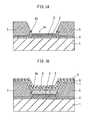
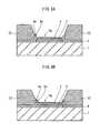
- FIGS. 1A and 1Beach show an end elevation to illustrate a technical problem of the conventional art
- FIG. 2is a plan view showing a part of an organic EL display in embodiment of the present invention.
- FIG. 3is an end elevation schematically showing a cross section of the part of the organic EL display in embodiment of the present invention.
- FIG. 4is an enlarged end elevation of a portion B enclosed by an alternate long and short dash line of FIG. 3 .
- FIGS. 5A , 5 B, and 5 Care each a process chart showing a method of manufacturing the organic EL display in embodiment of the present invention.
- FIGS. 6A , 6 B, and 6 Care each a process chart showing the method of manufacturing the organic EL display in embodiment of the present invention.
- FIGS. 7A , 7 B, and 7 Care each a process chart showing the method of manufacturing the organic EL display in embodiment of the present invention.
- FIG. 8is an end elevation schematically showing a cross section of a part of an organic EL display in modification of the present invention.
- FIGS. 9A and 9Bare each a process chart showing a method of manufacturing the organic EL display in modification of the present invention.
- FIG. 10is an end elevation schematically showing a cross section of a part of an organic EL display in modification of the present invention.
- FIG. 11is a plan view showing a part of an organic EL display in modification of the present invention.
- the inventorfound, through an intense study, that the uneven luminance can occur in the light-emitting surface and a life of the organic EL element can be reduced due to localized deterioration of the light-emitting layer.
- FIGS. 1A and 1Bare each an end elevation showing a manufacturing process of an organic EL display.
- FIG. 1Ashows a status in which a first electrode 2 , an ITO layer 3 , a hole injection layer 4 , and a bank 5 are formed on a TFT substrate 1 .
- FIG. 1Bshows a status in which a light-emitting layer 6 , an electron injection layer 7 , a second electrode 8 , and a passivation layer 9 are formed in addition to the components shown in FIG. 1A .
- a recess 4 ais formed in an upper surface of the hole injection layer 4 (see FIG. 1A ) in a process of forming the bank 5 .
- the light-emitting layer 6is formed with the recess 4 a formed in the upper surface of the hole injection layer 4 (see FIG. 1B )
- an electric fieldconcentrates in the vicinity of an upper peripheral edge 4 c of the recess 4 a when the organic EL display emits light.
- localized flow of currentcan occur in the light-emitting layer 6 . This might lead to the occurrence of uneven luminance in a light-emitting surface and reduce a life of the organic EL element due to localized deterioration of the light-emitting layer.
- the inventorarrived at the following technical features through a series of research and studies. That is, by covering the upper peripheral edge of the recess formed in the upper surface of the charge injection transport layer with a part of the bank, concentration of charges in the vicinity of the upper peripheral edge of the recess is suppressed when an organic EL element emits light. As a result, localized flow of current is suppressed.
- One aspect of the present inventionis a light-emitter comprising: a first electrode; a laminate that is disposed on the first electrode and includes a charge injection transport layer and a light-emitting layer; a second electrode that is disposed on the laminate; and a bank that defines an area in which the light-emitting layer is to be formed, wherein in the area defined by the bank, the charge injection transport layer has a recess in an upper surface thereof, and an upper peripheral edge of the recess is covered with a part of the bank.
- the electrical field concentration in the vicinity of the upper peripheral edge of the recessis suppressed when the light-emitter emits light.
- localized flow of currentis suppressed in the light-emitting layer. Therefore, an occurrence of uneven luminance in a light-emitting surface is suppressed, and the luminescence property is further improved.
- the charge injection transport layermay be made from a material that is eroded when exposed to a liquid used for forming the bank. With this structure, the recess is formed in a process of forming a bank without adding extra steps.
- the charge injection transport layermay be made from one of a metal oxide, a metal nitride, and a metal oxynitride. In general, these are hydrophilic materials. Therefore, the recess is formed in a washing process with pure water in the process of forming the bank.
- the part of the bankmay reach a bottom of the recess, and a side surface of the bank may slope upward from the bottom of the recess to a top of the bank.
- the part of the bankmay be out of contact with a bottom of the recess.
- a methodfor example, of heat-treating a bank material to make it fluid so that the upper peripheral edge of the recess is covered with a part of the bank material.
- the bankmay include an insulating material. With this structure, adjacent light-emitting layers are insulated from each other.
- the light-emitting layermay be an organic EL layer.
- the charge injection transport layermay extend laterally along a bottom surface of the bank.
- the upper peripheral edge of the recessmay be a convex portion composed of (i) a part of the upper surface of the charge injection transport layer in which the recess is not formed and (ii) an inner side surface of the recess.
- Another aspect of the present inventionis a light-emitting device comprising a plurality of light-emitters described above.
- Yet another aspect of the present inventionis a method of manufacturing a light-emitter including a first electrode, a laminate that is disposed on the first electrode and includes a charge injection transport layer and a light-emitting layer, a second electrode that is disposed on the laminate, and a bank that defines an area in which the light-emitting layer is to be formed, the method comprising the steps of: forming the charge injection transport layer; forming a bank material layer for forming the bank on the charge injection transport layer; removing a portion of the bank material layer to partially expose the charge injection transport layer; heat-treating a remaining portion of the bank material layer; and forming the light-emitting layer on an exposed surface of the charge injection transport layer after the heat treatment, wherein the charge injection transport layer is made from a material that is eroded when exposed to a liquid used while the charge injection transport layer is partially exposed, the charge injection transport layer has a recess in the exposed surface thereof so that a bottom of the recess is lower than a bottom surface of the remaining portion
- an organic EL element using an organic EL material as a light-emitting layeris taken as an example of the light-emitter
- an organic EL displayis taken as an example of the light-emitting device having a plurality of light-emitters. Note that the drawings are not to scale, so that proportions of members in the drawings are different from actual proportions.
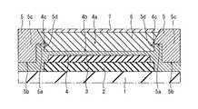
- FIG. 2is a plan view showing a part of an organic EL display in embodiment of the present invention.
- a organic EL display 100is a top-emission type organic EL display composed of organic EL elements 10 a , 10 b , and 10 c arranged in a matrix and each provided with a light emitting layer having a color of either red (R), green (G), or blue (B).
- Each organic EL elementfunctions as a sub-pixel, and three consecutive organic EL elements of colors of RGB function as a pixel as a whole.
- a pixel bank 55 having a lattice shapeis adopted.
- Each bank element 55 a extending along a Y axisdelimits consecutive light-emitting layers 56 a 1 , 56 b 1 , and 56 c 1 arranged along an X axis as well as consecutive light-emitting layers 56 a 2 , 56 b 2 , and 56 c 2 arranged along the X axis.
- a bank element 55 b extending along the X axisdelimits adjacent light-emitting layers 56 a 1 and 56 a 2 arranged along the Y axis, adjacent light-emitting layers 56 b 1 and 56 b 2 arranged along the Y axis, and adjacent light-emitting layers 56 c 1 and 56 c 2 arranged along the Y axis.
- FIG. 3is an end elevation schematically showing a cross section of a part of the organic EL display in embodiment of the present invention taken along the line A-A of FIG. 2 .
- FIG. 4is an enlarged end elevation of a portion B enclosed by an alternate long and short dash line of FIG. 3 .
- the first electrodes (anodes) 2are formed in a matrix.
- the ITO (indium tin oxide) layer 3 and the hole injection layer 4are laminated in the stated order. Note that, while the ITO layer 3 is laminated only on the first electrode 2 , the hole injection layer 4 is formed not only on the first electrode 2 but also over the substrate 1 .
- the bank 5is formed above a periphery of the first electrode 2 via the hole injection layer 4 .
- the light-emitting layer 6is laminated in an area defined by the bank 5 .
- the electron injection layer 7 , the second electrode (cathode) 8 , and the passivation layer 9are formed continuously across the consecutive organic EL elements 10 a , 10 b and 10 c , passing over the bank 5 .
- the substrate 1is made from an insulating material such as alkali-free glass, soda glass, nonluminescent glass, phosphate glass, boric-acid glass, quartz, acrylic resin, styrene resin, polycarbonate resin, epoxy resin, polyethylene, polyester, silicon resin, and alumina.
- an insulating materialsuch as alkali-free glass, soda glass, nonluminescent glass, phosphate glass, boric-acid glass, quartz, acrylic resin, styrene resin, polycarbonate resin, epoxy resin, polyethylene, polyester, silicon resin, and alumina.
- the first electrode 2is made of Ag (silver).
- the first electrode 2may be made of APC (alloy of silver, palladium and copper), ARA (alloy of silver, rubidium and gold), MoCr (alloy of molybdenum and chrome) or NiCr (alloy of nickel and chrome), for example.
- APCalloy of silver, palladium and copper
- ARAalloy of silver, rubidium and gold
- MoCralloy of molybdenum and chrome
- NiCralloy of nickel and chrome
- the ITO layer 3is interposed between the first electrode 2 and the hole injection layer 4 , and has a function of improving the bond between these layers.
- the hole injection layer 4is made from WOx (tungsten oxide) or MoxWyOz (molybdenum-tungsten oxide). Note that the hole injection layer 4 only has to be made from a metal compound performing a function of injecting holes. Examples of such a metal compound are a metal oxide, a metal nitride, and a metal oxynitride.
- the hole injection layer 4is made from a specific metal compound, it is easy to inject holes, and electrons contribute to light emission effectively in the light-emitting layer 6 . Therefore, favorable luminescence property is obtained.
- the specific metal compoundbe a transition metal.
- the oxidization number of a transition metalis plural, and therefore the transition metal can have a plurality of levels. As a result, it becomes easy to inject holes, and thus drive voltage is reduced.
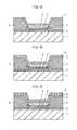
- the hole injection layer 4extends laterally along bottom surfaces 5 a and 5 b of the bank 5 , and has a recess 4 a in an upper surface thereof.
- a bottom 4 b of the recess 4 ais lower than a level 5 c of the bottom surface 5 a of the bank 5 .
- the recess 4 ais made up of the bottom 4 b and an inner side surface 4 d continuing the bottom 4 b .
- the depth of the recess 4 ais approximately 5 nm to 30 nm.
- An upper peripheral edge 4 c of the recessis a convex portion composed of (i) a part of the upper surface of the hole injection layer 4 in which the recess is not formed 4 e and (ii) the inner side surface 4 d of the recess.
- the upper peripheral edge 4 cis covered with a covering part 5 d , which is a part of the bank 5 .
- the upper peripheral edge 4 c of the recessprotrudes from the bottom 4 b of the recess. Therefore, if the upper peripheral edge 4 c is not covered with the covering part 5 d made from an insulating material, electric field concentrates in the vicinity of the upper peripheral edge 4 c of the recess, and localized flow of current occurs in the light-emitting layer 6 . As a result, the uneven luminance occurs in a light-emitting surface and a life of the organic EL element is reduced due to localized deterioration of the light-emitting layer 6 .
- the above-mentioned problemsare prevented, because the upper peripheral edge 4 c of the recess is covered with the covering part 5 d made from an insulating material.
- the thickness of the covering part 5 d(a shortest distance between the upper peripheral edge 4 c of the recess and the light-emitting layer 6 ) be 2 nm to 5 nm to effectively suppress the electric field concentration.
- the upper peripheral edge 4 c of the recesshas a right angle.
- the upper peripheral edge 4 c of the recessmay have a plurality of angles, or may be curved. In such a case, the electrical field concentration is further suppressed.
- the covering part 5 dreaches the bottom 4 b of the recess 4 a , and a side surface of the bank 5 slopes upward from the bottom 4 b of the recess to a top of the bank 5 .
- the bank 5partitions the light-emitting layer 6 into sub-pixels.
- the bank 5is made from an organic material, such as a resin, and has an insulating property. Examples of the organic material are an acrylic resin, a polyimide resin and a novolac-type phenolic resin. It is preferable that the bank 5 be resistant to organic solvent. Furthermore, the bank 5 can be subjected to an etching process, a baking process or the like. Therefore, it is preferable that the bank 5 be made from a highly resistant material so as not to be excessively deformed or degenerated by such processes.
- the light-emitting layer 6be made from a fluorescent material such as an oxinoid compound, perylene compound, coumarin compound, azacoumarin compound, oxazole compound, oxadiazole compound, perinone compound, pyrrolo-pyrrole compound, naphthalene compound, anthracene compound, fluorene compound, fluoranthene compound, tetracene compound, pyrene compound, coronene compound, quinolone compound and azaquinolone compound, pyrazoline derivative and pyrazolone derivative, rhodamine compound, chrysene compound, phenanthrene compound, cyclopentadiene compound, stilbene compound, diphenylquinone compound, styryl compound, butadiene compound, dicyanomethylene pyran compound, dicyanomethylene thiopyran compound, fluorescein compound, pyrylium compound, thiapyrylium compound, sel
- the electron injection layer 7has a function of transporting, to the light-emitting layer 6 , an electron injected from the second electrode 8 . It is preferable that the electron injection layer 7 be made from barium, phthalocyanine, fluorine lithium, or a combination of these materials.
- the second electrode 8is made of ITO, or IZO (indium zinc oxide), for example. In a case of a top-emission type light-emitter, it is preferable that the second electrode 8 be made of a light-transmissive material.
- the passivation layer 9has a function of preventing the light-emitting layer 6 and so on from being exposed to moisture and air.
- the passivation layer 9is made from a material such as SiN (silicon nitride) and SiON (silicon oxynitride).
- a top-emission type light-emitterpreferably includes the passivation layer 9 made of a light-transmissive material.
- FIGS. 5A , 5 B, 5 C, 6 A, 6 B, 6 C, 7 A, 7 B, and 7 Care each a process chart showing a method of manufacturing the organic EL display in embodiment of the present invention.
- a thin Ag filmis formed on the substrate 1 using a sputtering method.
- the formed thin Ag filmis then patterned using photolithography or the like to form the first electrodes 2 in a matrix.
- the thin Ag filmmay be formed using a vacuum evaporation method or the like.
- a thin ITO filmis formed using the sputtering method or the like.
- the formed thin ITO filmis then patterned using the photolithography or the like to form the ITO layer 3 .
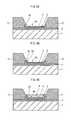
- a thin WOx film 11 or a thin MoxWyOz film 11is formed from a composition containing WOx or MoxWyOz using technology such as vacuum evaporation and sputtering.
- a bank material layer 12is formed on the thin film 11 .
- a portion of the bank material layer 12is removed so that the thin film 11 is partially exposed.
- the bank material layer 12is formed by application or the like.
- the portion of the bank material layer 12is removed by forming a resist pattern on the bank material layer 12 , and then performing etching.
- the resist patternis removed by an aqueous or non-aqueous release agent after the etching.
- the remaining portion of the bank material layer 12is made fluid to some extent by heat treatment so that a bank material extends to cover the upper peripheral edge 4 c of the recess.
- the upper peripheral edge 4 c of the recessis covered with the covering part 5 d in the above-mentioned manner.
- a heat curecan be adopted as the heat treatment, for example.
- the temperature and time for the heat curemay be appropriately determined in consideration of a type of the bank material and a required thickness of the covering part 5 d and so on.
- a surface of the remaining portion of the bank material layer 12is, for example, subjected to treatment using fluorine plasma and the like to provide liquid repellency as necessary, and, as a result, the bank 5 is formed.
- an ink composition including an organic EL material(hereinafter, simply referred to as “ink”) is dropped in the area defined by the bank 5 by the inkjet method or the like.
- the inkmay be dropped by a dispenser method, a nozzle-coat method, a spin coat method, an intaglio printing, a letter press printing, or the like.
- a thin barium film as the electron injection layer 7is formed using a vacuum evaporation method or the like.
- a thin ITO film as the second electrode 8is formed using a sputtering method.
- the passivation layer 9is further formed.
- the electrical field concentration in the vicinity of the upper peripheral edge 4 c of the recessis suppressed because the upper peripheral edge 4 c of the recess is covered with the covering part 5 d and the light-emitting layer 6 is formed on the covering part 5 d.
- WOx or MoxWyOzis used as a material for the hole injection layer 4 .
- a metal oxide, a metal nitride, and a metal oxynitrideare likely to be eroded by pure water. Therefore, even when a metal other than Mo (molybdenum) and W (tungsten) is used as a material for the hole injection layer 4 , a similar effect is obtained by applying the present embodiment.
- the recessis formed by the hole injection layer being eroded by pure water during washing.
- the recessmay be formed by the hole injection layer being eroded by etching solution during etching, or by the hole injection layer being eroded by a release agent during removal of the resist pattern.
- the present inventionis effective in a case where the hole injection layer is made from a material that is eroded when exposed to a liquid used for forming the bank, in particular, the hole injection layer is made from a material that is eroded when exposed to a liquid used while the hole injection layer is partially exposed.
- the covering part extending from the bankreaches the bottom 4 b of the recess beyond the upper peripheral edge 4 c of the recess.
- the present inventionis not limited to the above as long as at least the upper peripheral edge 4 c of the recess is covered.
- the covering part 5 dmay be out of contact with the bottom 4 b of the recess.
- the recess 4 ais formed in the hole injection layer 4 by washing after etching in the process of forming the bank.
- mask pattering or the likemay be used as a method of foaming the recess.
- FIG. 6Aalthough a lower end of the slope of the bank material 12 coincides with the upper peripheral edge 4 c of the recess, the structure of the bank material 12 is not limited to this.
- the part of the upper surface of the hole injection layer 4 in which the recess is not formed 4 emay be partially exposed by the slope of the bank material 12 being set back, as shown in FIG. 9A .
- the upper peripheral edge 4 c of the recessis covered with a part of the bank material (see FIG. 9B ).
- the present inventionis not limited to the above.
- a hole transport layer 13may be formed on the hole injection layer 4 , and these layers may be interposed as the charge injection transport layer.
- the recessis formed in an upper surface of the hole transport layer 13 , and an upper peripheral edge of the recess formed in the hole transport layer 13 is covered with the covering part.
- the ITO layer 3is formed on the first electrode 2 .
- the first electrode 2is formed from an Al-based material, it is possible to adopt a single layer structure of the anode without forming the ITO layer 3 .
- the organic EL displayis taken as an example of the light-emitting device having a plurality of light-emitters, the present invention is not limited to this.
- the present inventionmay be applied to a luminaire and the like.
- the present inventionis not limited to this.
- a line bank(banks arranged in lines) may be adopted.
- the line bank 65is adopted.
- the line bank 65delimits consecutive light-emitting layers 66 a , 66 b , and 66 c arranged along the X axis. Note that when the line bank 65 is adopted as shown in FIG. 11 , adjacent light-emitting layers arranged along the Y axis are not defined by the bank element. However, by appropriately determining a driving method, a size of the anode, an interval between the anodes and so on, the adjacent light-emitting layers emit light without influencing each other.
- the light-emitter of the present inventionis not limited to the top-emission type light-emitter.
- a bottom-emission type light-emittermay be adopted.
- the electron transport layermay be interposed in addition to the electron injection layer.
- the present inventionis applicable to an organic EL display and the like.
Landscapes
- Engineering & Computer Science (AREA)
- Physics & Mathematics (AREA)
- Optics & Photonics (AREA)
- Microelectronics & Electronic Packaging (AREA)
- Manufacturing & Machinery (AREA)
- Electroluminescent Light Sources (AREA)
Abstract
Description
- Japanese Patent Application Publication No. 2005-203339
Claims (20)
Applications Claiming Priority (3)
| Application Number | Priority Date | Filing Date | Title |
|---|---|---|---|
| JP2009028970 | 2009-02-10 | ||
| JP2009-028970 | 2009-02-10 | ||
| PCT/JP2010/000782WO2010092796A1 (en) | 2009-02-10 | 2010-02-09 | Light-emitting element, light-emitting device comprising light-emitting element, and method for manufacturing light-emitting element |
Related Parent Applications (1)
| Application Number | Title | Priority Date | Filing Date |
|---|---|---|---|
| PCT/JP2010/000782ContinuationWO2010092796A1 (en) | 2009-02-10 | 2010-02-09 | Light-emitting element, light-emitting device comprising light-emitting element, and method for manufacturing light-emitting element |
Publications (2)
| Publication Number | Publication Date |
|---|---|
| US20110291086A1 US20110291086A1 (en) | 2011-12-01 |
| US8866160B2true US8866160B2 (en) | 2014-10-21 |
Family
ID=42561646
Family Applications (1)
| Application Number | Title | Priority Date | Filing Date |
|---|---|---|---|
| US13/205,773ActiveUS8866160B2 (en) | 2009-02-10 | 2011-08-09 | Light-emitting element, device, and manufacturing method including a charge injection layer having a recess for suppressing uneven luminance |
Country Status (6)
| Country | Link |
|---|---|
| US (1) | US8866160B2 (en) |
| EP (1) | EP2398084B1 (en) |
| JP (1) | JP5357194B2 (en) |
| KR (1) | KR20110126594A (en) |
| CN (1) | CN102272970B (en) |
| WO (1) | WO2010092796A1 (en) |
Cited By (3)
| Publication number | Priority date | Publication date | Assignee | Title |
|---|---|---|---|---|
| US20140175411A1 (en)* | 2012-04-18 | 2014-06-26 | Panasonic Corporation | Organic el device |
| US9312519B2 (en) | 2012-06-01 | 2016-04-12 | Joled Inc. | Organic light emitting element, organic el display panel, organic el display device, coated device, and method for manufacturing these |
| US11917846B2 (en) | 2019-09-23 | 2024-02-27 | Lg Display Co., Ltd. | Display device having an oxide insulating film between subpixels and method for manufacturing the same |
Families Citing this family (32)
| Publication number | Priority date | Publication date | Assignee | Title |
|---|---|---|---|---|
| WO2010092796A1 (en) | 2009-02-10 | 2010-08-19 | パナソニック株式会社 | Light-emitting element, light-emitting device comprising light-emitting element, and method for manufacturing light-emitting element |
| CN102308671B (en) | 2009-02-10 | 2015-01-21 | 松下电器产业株式会社 | Manufacturing method of light-emitting element, light-emitting element, and manufacturing method of light-emitting device, and light-emitting device |
| WO2010092797A1 (en)* | 2009-02-10 | 2010-08-19 | パナソニック株式会社 | Light-emitting element, display device, and method for manufacturing light-emitting element |
| JP5437736B2 (en) | 2009-08-19 | 2014-03-12 | パナソニック株式会社 | Organic EL device |
| WO2011161727A1 (en) | 2010-06-24 | 2011-12-29 | パナソニック株式会社 | Method for producing organic el element, display device, light-emitting device, and ultraviolet irradiation device |
| CN102473847B (en) | 2010-06-24 | 2015-01-14 | 松下电器产业株式会社 | Organic el element, display apparatus, and light-emitting apparatus |
| JP5624141B2 (en) | 2010-07-30 | 2014-11-12 | パナソニック株式会社 | Organic EL device |
| WO2012017496A1 (en) | 2010-08-06 | 2012-02-09 | パナソニック株式会社 | Light emitting device, light emitting apparatus provided with a light emitting device, and method of manufacturing a light emitting device |
| JP5677437B2 (en) | 2010-08-06 | 2015-02-25 | パナソニック株式会社 | Organic EL device |
| WO2012017489A1 (en) | 2010-08-06 | 2012-02-09 | パナソニック株式会社 | Organic el element, display device, and light-emitting device |
| JP5677436B2 (en) | 2010-08-06 | 2015-02-25 | パナソニック株式会社 | Organic EL device |
| JP5677433B2 (en) | 2010-08-06 | 2015-02-25 | パナソニック株式会社 | ORGANIC EL ELEMENT, DISPLAY DEVICE AND LIGHT EMITTING DEVICE |
| WO2012017485A1 (en) | 2010-08-06 | 2012-02-09 | パナソニック株式会社 | Organic el element, display device, and light-emitting device |
| CN103038908B (en) | 2010-08-06 | 2016-01-06 | 株式会社日本有机雷特显示器 | Light-emitting component, possess the light-emitting device of light-emitting component and the manufacture method of light-emitting component |
| WO2012017497A1 (en) | 2010-08-06 | 2012-02-09 | パナソニック株式会社 | Organic el element |
| JP5612691B2 (en) | 2010-08-06 | 2014-10-22 | パナソニック株式会社 | Organic EL device and method for manufacturing the same |
| JP5543599B2 (en) | 2010-08-06 | 2014-07-09 | パナソニック株式会社 | Method for manufacturing light emitting device |
| WO2012017501A1 (en) | 2010-08-06 | 2012-02-09 | パナソニック株式会社 | Organic electroluminescence element and method of manufacturing thereof |
| JP5612693B2 (en) | 2010-08-06 | 2014-10-22 | パナソニック株式会社 | Organic EL device and method for manufacturing the same |
| WO2012017492A1 (en) | 2010-08-06 | 2012-02-09 | パナソニック株式会社 | Light emitting element, method for manufacturing same, and light emitting device |
| JP5574456B2 (en)* | 2010-08-06 | 2014-08-20 | パナソニック株式会社 | LIGHT EMITTING ELEMENT, MANUFACTURING METHOD THEREOF, AND LIGHT EMITTING DEVICE |
| JP5620494B2 (en) | 2010-08-06 | 2014-11-05 | パナソニック株式会社 | LIGHT EMITTING ELEMENT, DISPLAY DEVICE, AND METHOD FOR MANUFACTURING LIGHT EMITTING ELEMENT |
| CN103283054B (en) | 2011-01-21 | 2015-12-16 | 株式会社日本有机雷特显示器 | Organic el element |
| WO2012114648A1 (en) | 2011-02-23 | 2012-08-30 | パナソニック株式会社 | Organic electroluminescence display panel and organic electroluminescence display device |
| JP5809234B2 (en) | 2011-02-25 | 2015-11-10 | 株式会社Joled | Organic EL display panel and organic EL display device |
| WO2012153445A1 (en) | 2011-05-11 | 2012-11-15 | パナソニック株式会社 | Organic el display panel and organic el display device |
| JP5520418B2 (en)* | 2011-05-20 | 2014-06-11 | パナソニック株式会社 | Organic electroluminescence device |
| CN107393939B (en)* | 2017-08-30 | 2020-04-17 | 京东方科技集团股份有限公司 | Pixel defining layer and manufacturing method thereof, display panel and manufacturing method thereof, and display device |
| CN114616923B (en)* | 2019-11-07 | 2025-04-01 | 夏普株式会社 | Light emitting element, display device, and method for manufacturing light emitting element |
| CN112133734B (en)* | 2020-09-29 | 2022-08-30 | 湖北长江新型显示产业创新中心有限公司 | Display panel and display device |
| CN118488741A (en)* | 2021-11-29 | 2024-08-13 | 京东方科技集团股份有限公司 | Display substrate |
| KR20230102192A (en)* | 2021-12-30 | 2023-07-07 | 엘지디스플레이 주식회사 | Display device |
Citations (111)
| Publication number | Priority date | Publication date | Assignee | Title |
|---|---|---|---|---|
| JPH05163488A (en) | 1991-12-17 | 1993-06-29 | Konica Corp | Electroluminescent element of organic thin film |
| US5294869A (en) | 1991-12-30 | 1994-03-15 | Eastman Kodak Company | Organic electroluminescent multicolor image display device |
| US5443922A (en) | 1991-11-07 | 1995-08-22 | Konica Corporation | Organic thin film electroluminescence element |
| US5688551A (en) | 1995-11-13 | 1997-11-18 | Eastman Kodak Company | Method of forming an organic electroluminescent display panel |
| JPH10162959A (en) | 1996-11-29 | 1998-06-19 | Idemitsu Kosan Co Ltd | Organic electroluminescence device |
| JP2000133446A (en) | 1998-10-28 | 2000-05-12 | Tdk Corp | Manufacturing apparatus and manufacturing method of organic EL display device |
| JP2000223276A (en) | 1999-02-02 | 2000-08-11 | Idemitsu Kosan Co Ltd | Organic electroluminescence device and method of manufacturing the same |
| US6284393B1 (en) | 1996-11-29 | 2001-09-04 | Idemitsu Kosan Co., Ltd. | Organic electroluminescent device |
| US6309801B1 (en) | 1998-11-18 | 2001-10-30 | U.S. Philips Corporation | Method of manufacturing an electronic device comprising two layers of organic-containing material |
| JP2002075661A (en) | 2000-08-31 | 2002-03-15 | Fujitsu Ltd | Organic EL element and organic EL display device |
| US20020051894A1 (en) | 2000-08-31 | 2002-05-02 | Fujitsu Limited | Organic EL element and method of manufacturing the same, organic EL display device using the element, organic EL material, and surface emission device and liquid crystal display device using the material |
| JP2002318556A (en) | 2001-04-20 | 2002-10-31 | Toshiba Corp | Active matrix type flat display device and manufacturing method thereof |
| US20020158835A1 (en) | 2001-04-20 | 2002-10-31 | Michiya Kobayashi | Display device and method of manufacturing the same |
| JP2003007460A (en) | 2001-06-22 | 2003-01-10 | Sony Corp | Method for manufacturing display equipment, and display equipment |
| US20030137242A1 (en) | 2001-12-18 | 2003-07-24 | Seiko Epson Corporation | Display apparatus, electric device, and manufacturing method of display apparatus |
| JP2003264083A (en) | 2002-03-08 | 2003-09-19 | Sharp Corp | Organic LED element and manufacturing method thereof |
| US20040075385A1 (en) | 2002-08-12 | 2004-04-22 | Ye Tao | Photoresist mask/smoothing layer ensuring the field homogeneity and better step-coverage in OLED displays |
| JP2004139746A (en) | 2002-10-15 | 2004-05-13 | Denso Corp | Method for manufacturing organic el element |
| JP2004228355A (en) | 2003-01-23 | 2004-08-12 | Seiko Epson Corp | Insulating film substrate manufacturing method, insulating film substrate manufacturing apparatus, insulating film substrate, electro-optical device manufacturing method, and electro-optical device |
| JP2004234901A (en) | 2003-01-28 | 2004-08-19 | Seiko Epson Corp | Display substrate, organic EL display device, display substrate manufacturing method and electronic device |
| JP2004527093A (en) | 2001-05-18 | 2004-09-02 | ケンブリッジ・ユニバーシティ・テクニカル・サービシズ・リミテッド | Electroluminescence device |
| JP2004363170A (en) | 2003-06-02 | 2004-12-24 | Seiko Epson Corp | Method of forming conductive pattern, electro-optical device, method of manufacturing electro-optical device, and electronic apparatus |
| JP2005012173A (en) | 2003-05-28 | 2005-01-13 | Seiko Epson Corp | Film pattern forming method, device and device manufacturing method, electro-optical device, and electronic apparatus |
| US20050093432A1 (en)* | 2003-09-19 | 2005-05-05 | Shunpei Yamazaki | Display device and method for manufacturing the same |
| US20050093434A1 (en) | 2003-09-22 | 2005-05-05 | Suh Min-Chul | Full color organic light-emtting device having color modulation layer |
| JP2005197189A (en) | 2004-01-09 | 2005-07-21 | Seiko Epson Corp | Electro-optical device manufacturing method and electronic apparatus |
| JP2005203339A (en) | 2003-12-16 | 2005-07-28 | Matsushita Electric Ind Co Ltd | Organic electroluminescent device and manufacturing method thereof |
| JP2005203340A (en) | 2003-12-16 | 2005-07-28 | Matsushita Electric Ind Co Ltd | Organic electroluminescent device |
| US20050170208A1 (en) | 2003-12-16 | 2005-08-04 | Matsushita Electric Industrial Co., Ltd. | Organic electroluminescent device and method for manufacturing the same |
| JP2005268099A (en) | 2004-03-19 | 2005-09-29 | Mitsubishi Electric Corp | Organic EL display panel, organic EL display device, and method of manufacturing organic EL display panel |
| JP2005267926A (en) | 2004-03-17 | 2005-09-29 | Japan Science & Technology Agency | Double-sided organic EL panel |
| US20050266763A1 (en) | 2004-05-27 | 2005-12-01 | Seiko Epson Corporation | Method of manufacturing color filter substrate, method of manufacturing electro-optical device, electro-optical device, and electronic apparatus |
| JP2005331665A (en) | 2004-05-19 | 2005-12-02 | Seiko Epson Corp | ELECTRO-OPTICAL DEVICE, MANUFACTURING METHOD THEREOF, AND ELECTRONIC DEVICE |
| US20060008931A1 (en) | 2004-07-09 | 2006-01-12 | Au Optronics Corporation | Method for electro-luminescent display fabrication |
| JP2006114928A (en) | 2005-12-09 | 2006-04-27 | Idemitsu Kosan Co Ltd | N-type inorganic semiconductor, n-type inorganic semiconductor thin film, and manufacturing method thereof |
| US20060139342A1 (en)* | 2004-12-29 | 2006-06-29 | Gang Yu | Electronic devices and processes for forming electronic devices |
| JP2006185869A (en) | 2004-12-28 | 2006-07-13 | Asahi Glass Co Ltd | Organic electroluminescent device and manufacturing method thereof |
| DE102005007540A1 (en)* | 2005-02-18 | 2006-08-31 | Robert Bosch Gmbh | Micromechanical membrane sensor with double membrane |
| JP2006253443A (en) | 2005-03-11 | 2006-09-21 | Seiko Epson Corp | ORGANIC EL DEVICE, ITS MANUFACTURING METHOD, AND ELECTRONIC DEVICE |
| JP2006294261A (en) | 2005-04-05 | 2006-10-26 | Fuji Electric Holdings Co Ltd | ORGANIC EL LIGHT EMITTING ELEMENT AND MANUFACTURING METHOD THEREOF |
| US20060243377A1 (en) | 2005-04-27 | 2006-11-02 | Keisuke Matsuo | Transfer method and transfer apparatus |
| JP2006344459A (en) | 2005-06-08 | 2006-12-21 | Sony Corp | Transfer method and transfer device |
| US20060284166A1 (en) | 2003-05-12 | 2006-12-21 | Cambridge University Technical Services Limited | Polymer transistor |
| US20070029929A1 (en) | 2005-08-08 | 2007-02-08 | Semiconductor Energy Laboratory Co., Ltd. | Light emitting device and manufacturing method thereof |
| JP2007073499A (en) | 2005-08-08 | 2007-03-22 | Semiconductor Energy Lab Co Ltd | Light-emitting device and its manufacturing method |
| WO2007037358A1 (en)* | 2005-09-29 | 2007-04-05 | Matsushita Electric Industrial Co., Ltd. | Organic el display and method for manufacturing same |
| JP2007095606A (en) | 2005-09-30 | 2007-04-12 | Seiko Epson Corp | ORGANIC EL DEVICE, ITS MANUFACTURING METHOD, AND ELECTRONIC DEVICE |
| US20070099396A1 (en)* | 2005-10-27 | 2007-05-03 | Seiko Epson Corporation | Method of forming pattern, film structure, electrooptical device and electronic equipment |
| US20070172978A1 (en) | 2003-05-12 | 2007-07-26 | Cambridge University Technical Service Limited | Manufacture of a polymer device |
| JP2007214066A (en) | 2006-02-13 | 2007-08-23 | Seiko Epson Corp | Method for manufacturing organic electroluminescent device |
| JP2007220656A (en) | 2006-01-18 | 2007-08-30 | Toppan Printing Co Ltd | Organic electroluminescence device and method for manufacturing the same |
| US20070241665A1 (en) | 2006-04-12 | 2007-10-18 | Matsushita Electric Industrial Co., Ltd. | Organic electroluminescent element, and manufacturing method thereof, as well as display device and exposure apparatus using the same |
| JP2007288071A (en) | 2006-04-19 | 2007-11-01 | Matsushita Electric Ind Co Ltd | ORGANIC ELECTROLUMINESCENT ELEMENT AND ITS MANUFACTURING METHOD, DISPLAY DEVICE USING THE SAME, AND EXPOSURE DEVICE |
| JP2007288074A (en) | 2006-04-19 | 2007-11-01 | Matsushita Electric Ind Co Ltd | Organic electroluminescent device and manufacturing method thereof |
| JP2007287353A (en) | 2006-04-12 | 2007-11-01 | Matsushita Electric Ind Co Ltd | Method for manufacturing organic electroluminescent element and organic electroluminescent element produced using the same |
| US20070290604A1 (en) | 2006-06-16 | 2007-12-20 | Matsushita Electric Industrial Co., Ltd. | Organic electroluminescent device and method of producing the same |
| JP2008041747A (en) | 2006-08-02 | 2008-02-21 | Matsushita Electric Ind Co Ltd | Organic electroluminescent light emitting device and manufacturing method thereof |
| JP2008053556A (en) | 2006-08-25 | 2008-03-06 | Matsushita Electric Works Ltd | Organic electroluminescence device |
| JP2008091072A (en) | 2006-09-29 | 2008-04-17 | Seiko Epson Corp | Electro-optical device and manufacturing method thereof |
| JP2008124268A (en) | 2006-11-13 | 2008-05-29 | Matsushita Electric Works Ltd | Organic electroluminescence device |
| JP2008140724A (en) | 2006-12-05 | 2008-06-19 | Toppan Printing Co Ltd | Method for manufacturing organic EL element and organic EL element |
| US20080150422A1 (en) | 2006-12-21 | 2008-06-26 | Semiconductor Energy Laboratory Co., Ltd. | Light-emitting element and light-emitting device |
| JP2008218250A (en)* | 2007-03-06 | 2008-09-18 | Casio Comput Co Ltd | Display device and manufacturing method thereof |
| US20080231179A1 (en) | 2007-03-23 | 2008-09-25 | Toppan Printing Co., Ltd. | Organic Electroluminescence Element and Display Using the Same |
| JP2008241238A (en) | 2008-05-28 | 2008-10-09 | Mitsubishi Electric Corp | Refrigeration air conditioner and control method of refrigeration air conditioner |
| WO2008120714A1 (en) | 2007-03-29 | 2008-10-09 | Dai Nippon Printing Co., Ltd. | Organic electroluminescent element and process for producing the same |
| WO2008149498A1 (en)* | 2007-05-31 | 2008-12-11 | Panasonic Corporation | Organic el device and method for manufacturing the same |
| WO2008149499A1 (en) | 2007-05-30 | 2008-12-11 | Panasonic Corporation | Organic el display panel and method for manufacturing the same |
| JP2009004347A (en) | 2007-05-18 | 2009-01-08 | Toppan Printing Co Ltd | Manufacturing method of organic EL display element and organic EL display element |
| JP2009044103A (en) | 2007-08-10 | 2009-02-26 | Sumitomo Chemical Co Ltd | Organic electroluminescence device and manufacturing method |
| JP2009048960A (en) | 2007-08-23 | 2009-03-05 | Canon Inc | Electrode cleaning method |
| JP2009054582A (en) | 2007-07-31 | 2009-03-12 | Sumitomo Chemical Co Ltd | Organic electroluminescence device and method for producing the same |
| JP2009058897A (en) | 2007-09-03 | 2009-03-19 | Hitachi Displays Ltd | Display device |
| US20090096364A1 (en)* | 2007-10-11 | 2009-04-16 | Gen Fujii | Display Device and Method for Manufacturing Display Device |
| US20090115318A1 (en) | 2005-08-23 | 2009-05-07 | Cambridge Display Technology Limited | Organic electronic device structures and fabrication methods |
| US20090160325A1 (en) | 2003-12-16 | 2009-06-25 | Panasonic Corporation | Organic electroluminescent device and method for manufacturing the same |
| WO2009107323A1 (en)* | 2008-02-28 | 2009-09-03 | パナソニック株式会社 | Organic el display panel |
| JP2009218156A (en)* | 2008-03-12 | 2009-09-24 | Casio Comput Co Ltd | El panel and method of manufacturing el panel |
| US20090243478A1 (en) | 2008-03-26 | 2009-10-01 | Toppan Printing Co., Ltd. | Organic Electroluminescence Element, Method for Manufacturing the Same and Organic Electroluminescence Display Device |
| JP2009239180A (en) | 2008-03-28 | 2009-10-15 | Sumitomo Chemical Co Ltd | Organic electroluminescent device |
| US20090284144A1 (en) | 2008-05-16 | 2009-11-19 | Sony Corporation | Display unit |
| US20090284141A1 (en) | 2008-05-13 | 2009-11-19 | Panasonic Corporation | Organic electroluminescence element and manufacturing method thereof |
| US20090315027A1 (en) | 2008-06-24 | 2009-12-24 | Casio Computer Co., Ltd. | Light emitting device and manufacturing method of light emitting device |
| JP2010009746A (en)* | 2008-06-24 | 2010-01-14 | Casio Comput Co Ltd | Light emitting device and method for manufacturing of light emitting device |
| JP2010010670A (en) | 2008-05-28 | 2010-01-14 | Panasonic Corp | Light emitting device and method of manufacturing the same |
| JP2010021138A (en) | 2008-06-09 | 2010-01-28 | Panasonic Corp | Organic electroluminescent device and its manufacturing method |
| JP2010021162A (en) | 2007-12-10 | 2010-01-28 | Panasonic Corp | Organic el device, el display panel and methods of manufacturing organic el device and el display panel |
| JP2010033972A (en) | 2008-07-30 | 2010-02-12 | Sumitomo Chemical Co Ltd | Organic electroluminescent element and its manufacturing method |
| WO2010032444A1 (en) | 2008-09-19 | 2010-03-25 | パナソニック株式会社 | Organic electroluminescence element and method for manufacturing same |
| JP2010073700A (en) | 2007-12-28 | 2010-04-02 | Panasonic Corp | Organic el device and organic el display panel |
| US20100102310A1 (en) | 2008-10-24 | 2010-04-29 | Panasonic Corporation | Organic electroluminescence device and manufacturing method thereof |
| WO2010058716A1 (en) | 2008-11-19 | 2010-05-27 | 富士フイルム株式会社 | Organic electroluminescent element |
| WO2010070798A1 (en) | 2008-12-18 | 2010-06-24 | パナソニック株式会社 | Organic electroluminescent display device and method for manufacturing same |
| JP2010161185A (en) | 2009-01-08 | 2010-07-22 | Ulvac Japan Ltd | Organic el display device and method of manufacturing the same |
| JP2010161070A (en) | 2008-12-10 | 2010-07-22 | Panasonic Corp | Methods of manufacturing optical element and display device including the optical element |
| US20100188376A1 (en)* | 2008-12-24 | 2010-07-29 | Sony Corporation | Display device |
| WO2010092797A1 (en) | 2009-02-10 | 2010-08-19 | パナソニック株式会社 | Light-emitting element, display device, and method for manufacturing light-emitting element |
| WO2010092796A1 (en) | 2009-02-10 | 2010-08-19 | パナソニック株式会社 | Light-emitting element, light-emitting device comprising light-emitting element, and method for manufacturing light-emitting element |
| US20110018007A1 (en)* | 2007-11-30 | 2011-01-27 | Sumitomo Chemical Company, Limited | Electronic device, display apparatus, and electronic device manufacturing method |
| US20110037068A1 (en) | 2009-07-31 | 2011-02-17 | Semiconductor Energy Laboratory Co., Ltd. | Semiconductor device and method for manufacturing the same |
| US20110037065A1 (en) | 2008-04-28 | 2011-02-17 | Dai Nippon Printing Co., Ltd. | Device comprising positive hole injection transport layer, method for producing the same and ink for forming positive hole injection transport layer |
| WO2011021343A1 (en) | 2009-08-19 | 2011-02-24 | パナソニック株式会社 | Organic el element |
| JP2011040167A (en) | 2008-11-12 | 2011-02-24 | Panasonic Corp | Display and its manufacturing method |
| US20110180821A1 (en) | 2009-12-22 | 2011-07-28 | Panasonic Corporation | Display device and manufacturing method thereof |
| US20110193107A1 (en) | 2009-08-31 | 2011-08-11 | Panasonic Corporation | Light-emitter, method of manufacturing the same and light emitting device |
| US20110198623A1 (en) | 2009-12-22 | 2011-08-18 | Panasonic Corporation | Display device and manufacturing method thereof |
| US20110198624A1 (en) | 2009-12-22 | 2011-08-18 | Panasonic Corporation | Display device and manufacturing method thereof |
| US20110204410A1 (en) | 2010-02-22 | 2011-08-25 | Panasonic Corporation | Light-emitting device and manufacturing method thereof |
| WO2012017502A1 (en) | 2010-08-06 | 2012-02-09 | パナソニック株式会社 | Organic electroluminescence element and method of manufacturing thereof |
| WO2012017495A1 (en) | 2010-08-06 | 2012-02-09 | パナソニック株式会社 | Organic el element and production method for same |
| WO2012017503A1 (en) | 2010-08-06 | 2012-02-09 | パナソニック株式会社 | Organic electroluminescence element |
- 2010
- 2010-02-09WOPCT/JP2010/000782patent/WO2010092796A1/enactiveApplication Filing
- 2010-02-09KRKR1020117016574Apatent/KR20110126594A/ennot_activeCeased
- 2010-02-09JPJP2010550454Apatent/JP5357194B2/enactiveActive
- 2010-02-09CNCN201080004030.XApatent/CN102272970B/enactiveActive
- 2010-02-09EPEP10741076.3Apatent/EP2398084B1/enactiveActive
- 2011
- 2011-08-09USUS13/205,773patent/US8866160B2/enactiveActive
Patent Citations (149)
| Publication number | Priority date | Publication date | Assignee | Title |
|---|---|---|---|---|
| US5443922A (en) | 1991-11-07 | 1995-08-22 | Konica Corporation | Organic thin film electroluminescence element |
| JPH05163488A (en) | 1991-12-17 | 1993-06-29 | Konica Corp | Electroluminescent element of organic thin film |
| US5294869A (en) | 1991-12-30 | 1994-03-15 | Eastman Kodak Company | Organic electroluminescent multicolor image display device |
| JP3369615B2 (en) | 1991-12-30 | 2003-01-20 | イーストマン コダック カンパニー | Light emitting device |
| US5688551A (en) | 1995-11-13 | 1997-11-18 | Eastman Kodak Company | Method of forming an organic electroluminescent display panel |
| JP3789991B2 (en) | 1995-11-13 | 2006-06-28 | イーストマン コダック カンパニー | Donor sheet for thermal transfer of organic electroluminescent medium and method for producing full-color organic electroluminescent display device |
| JPH10162959A (en) | 1996-11-29 | 1998-06-19 | Idemitsu Kosan Co Ltd | Organic electroluminescence device |
| US6284393B1 (en) | 1996-11-29 | 2001-09-04 | Idemitsu Kosan Co., Ltd. | Organic electroluminescent device |
| JP2000133446A (en) | 1998-10-28 | 2000-05-12 | Tdk Corp | Manufacturing apparatus and manufacturing method of organic EL display device |
| US6132280A (en) | 1998-10-28 | 2000-10-17 | Tdk Corporation | System and process for fabricating an organic electroluminescent display device |
| JP2002530881A (en) | 1998-11-18 | 2002-09-17 | コーニンクレッカ フィリップス エレクトロニクス エヌ ヴィ | Method of manufacturing an electronic device having two layers of organic-containing material |
| US6309801B1 (en) | 1998-11-18 | 2001-10-30 | U.S. Philips Corporation | Method of manufacturing an electronic device comprising two layers of organic-containing material |
| JP2000223276A (en) | 1999-02-02 | 2000-08-11 | Idemitsu Kosan Co Ltd | Organic electroluminescence device and method of manufacturing the same |
| US20060204788A1 (en) | 2000-08-31 | 2006-09-14 | Fujitsu Limited | Organic EL element and method of manufacturing the same, organic EL display device using the element, organic EL material, and surface emission device and liquid crystal display device using the material |
| US20050208206A1 (en) | 2000-08-31 | 2005-09-22 | Fujitsu Limited | Organic EL element and method of manufacturing the same, organic EL display device using the element, organic EL material, and surface emission device and liquid crystal display device using the material |
| US20020051894A1 (en) | 2000-08-31 | 2002-05-02 | Fujitsu Limited | Organic EL element and method of manufacturing the same, organic EL display device using the element, organic EL material, and surface emission device and liquid crystal display device using the material |
| JP2002075661A (en) | 2000-08-31 | 2002-03-15 | Fujitsu Ltd | Organic EL element and organic EL display device |
| US20020158835A1 (en) | 2001-04-20 | 2002-10-31 | Michiya Kobayashi | Display device and method of manufacturing the same |
| JP2002318556A (en) | 2001-04-20 | 2002-10-31 | Toshiba Corp | Active matrix type flat display device and manufacturing method thereof |
| US20040178414A1 (en) | 2001-05-18 | 2004-09-16 | Gitti Frey | Electroluminescent device |
| JP2004527093A (en) | 2001-05-18 | 2004-09-02 | ケンブリッジ・ユニバーシティ・テクニカル・サービシズ・リミテッド | Electroluminescence device |
| JP2003007460A (en) | 2001-06-22 | 2003-01-10 | Sony Corp | Method for manufacturing display equipment, and display equipment |
| JP2003249375A (en) | 2001-12-18 | 2003-09-05 | Seiko Epson Corp | Display device, electronic device, and method of manufacturing display device |
| US20030137242A1 (en) | 2001-12-18 | 2003-07-24 | Seiko Epson Corporation | Display apparatus, electric device, and manufacturing method of display apparatus |
| JP2003264083A (en) | 2002-03-08 | 2003-09-19 | Sharp Corp | Organic LED element and manufacturing method thereof |
| US20040075385A1 (en) | 2002-08-12 | 2004-04-22 | Ye Tao | Photoresist mask/smoothing layer ensuring the field homogeneity and better step-coverage in OLED displays |
| JP2004139746A (en) | 2002-10-15 | 2004-05-13 | Denso Corp | Method for manufacturing organic el element |
| JP2004228355A (en) | 2003-01-23 | 2004-08-12 | Seiko Epson Corp | Insulating film substrate manufacturing method, insulating film substrate manufacturing apparatus, insulating film substrate, electro-optical device manufacturing method, and electro-optical device |
| JP2004234901A (en) | 2003-01-28 | 2004-08-19 | Seiko Epson Corp | Display substrate, organic EL display device, display substrate manufacturing method and electronic device |
| US20060284166A1 (en) | 2003-05-12 | 2006-12-21 | Cambridge University Technical Services Limited | Polymer transistor |
| US20070172978A1 (en) | 2003-05-12 | 2007-07-26 | Cambridge University Technical Service Limited | Manufacture of a polymer device |
| JP2007527542A (en) | 2003-05-12 | 2007-09-27 | ケンブリッジ エンタープライズ リミティド | Manufacture of polymer devices |
| US20050064633A1 (en) | 2003-05-28 | 2005-03-24 | Seiko Epson Corporation | Film pattern formation method, device and method for manufacturing the same, electro-optical device, electronic device, and method for manufacturing active matrix substrate |
| JP2005012173A (en) | 2003-05-28 | 2005-01-13 | Seiko Epson Corp | Film pattern forming method, device and device manufacturing method, electro-optical device, and electronic apparatus |
| JP2004363170A (en) | 2003-06-02 | 2004-12-24 | Seiko Epson Corp | Method of forming conductive pattern, electro-optical device, method of manufacturing electro-optical device, and electronic apparatus |
| US20050093432A1 (en)* | 2003-09-19 | 2005-05-05 | Shunpei Yamazaki | Display device and method for manufacturing the same |
| US20050093434A1 (en) | 2003-09-22 | 2005-05-05 | Suh Min-Chul | Full color organic light-emtting device having color modulation layer |
| JP2005203339A (en) | 2003-12-16 | 2005-07-28 | Matsushita Electric Ind Co Ltd | Organic electroluminescent device and manufacturing method thereof |
| US20090160325A1 (en) | 2003-12-16 | 2009-06-25 | Panasonic Corporation | Organic electroluminescent device and method for manufacturing the same |
| US20050170208A1 (en) | 2003-12-16 | 2005-08-04 | Matsushita Electric Industrial Co., Ltd. | Organic electroluminescent device and method for manufacturing the same |
| JP2005203340A (en) | 2003-12-16 | 2005-07-28 | Matsushita Electric Ind Co Ltd | Organic electroluminescent device |
| JP2005197189A (en) | 2004-01-09 | 2005-07-21 | Seiko Epson Corp | Electro-optical device manufacturing method and electronic apparatus |
| JP2005267926A (en) | 2004-03-17 | 2005-09-29 | Japan Science & Technology Agency | Double-sided organic EL panel |
| JP2005268099A (en) | 2004-03-19 | 2005-09-29 | Mitsubishi Electric Corp | Organic EL display panel, organic EL display device, and method of manufacturing organic EL display panel |
| JP2005331665A (en) | 2004-05-19 | 2005-12-02 | Seiko Epson Corp | ELECTRO-OPTICAL DEVICE, MANUFACTURING METHOD THEREOF, AND ELECTRONIC DEVICE |
| US20050266763A1 (en) | 2004-05-27 | 2005-12-01 | Seiko Epson Corporation | Method of manufacturing color filter substrate, method of manufacturing electro-optical device, electro-optical device, and electronic apparatus |
| JP2006024573A (en) | 2004-07-09 | 2006-01-26 | Au Optronics Corp | Electroluminescence display |
| US20060008931A1 (en) | 2004-07-09 | 2006-01-12 | Au Optronics Corporation | Method for electro-luminescent display fabrication |
| JP2006185869A (en) | 2004-12-28 | 2006-07-13 | Asahi Glass Co Ltd | Organic electroluminescent device and manufacturing method thereof |
| US20060139342A1 (en)* | 2004-12-29 | 2006-06-29 | Gang Yu | Electronic devices and processes for forming electronic devices |
| DE102005007540A1 (en)* | 2005-02-18 | 2006-08-31 | Robert Bosch Gmbh | Micromechanical membrane sensor with double membrane |
| US20090206422A1 (en)* | 2005-02-18 | 2009-08-20 | Matthias Illing | Micromechanical diaphragm sensor having a double diaphragm |
| JP2006253443A (en) | 2005-03-11 | 2006-09-21 | Seiko Epson Corp | ORGANIC EL DEVICE, ITS MANUFACTURING METHOD, AND ELECTRONIC DEVICE |
| JP2006294261A (en) | 2005-04-05 | 2006-10-26 | Fuji Electric Holdings Co Ltd | ORGANIC EL LIGHT EMITTING ELEMENT AND MANUFACTURING METHOD THEREOF |
| US20060243377A1 (en) | 2005-04-27 | 2006-11-02 | Keisuke Matsuo | Transfer method and transfer apparatus |
| JP2006344459A (en) | 2005-06-08 | 2006-12-21 | Sony Corp | Transfer method and transfer device |
| US20070029929A1 (en) | 2005-08-08 | 2007-02-08 | Semiconductor Energy Laboratory Co., Ltd. | Light emitting device and manufacturing method thereof |
| JP2007073499A (en) | 2005-08-08 | 2007-03-22 | Semiconductor Energy Lab Co Ltd | Light-emitting device and its manufacturing method |
| US20090115318A1 (en) | 2005-08-23 | 2009-05-07 | Cambridge Display Technology Limited | Organic electronic device structures and fabrication methods |
| WO2007037358A1 (en)* | 2005-09-29 | 2007-04-05 | Matsushita Electric Industrial Co., Ltd. | Organic el display and method for manufacturing same |
| US20090058268A1 (en)* | 2005-09-29 | 2009-03-05 | Matsushita Electric Industrial Co., Ltd. | Organic el display and method for manufacturing same |
| JP2007095606A (en) | 2005-09-30 | 2007-04-12 | Seiko Epson Corp | ORGANIC EL DEVICE, ITS MANUFACTURING METHOD, AND ELECTRONIC DEVICE |
| US20070099396A1 (en)* | 2005-10-27 | 2007-05-03 | Seiko Epson Corporation | Method of forming pattern, film structure, electrooptical device and electronic equipment |
| JP2006114928A (en) | 2005-12-09 | 2006-04-27 | Idemitsu Kosan Co Ltd | N-type inorganic semiconductor, n-type inorganic semiconductor thin film, and manufacturing method thereof |
| JP2007220656A (en) | 2006-01-18 | 2007-08-30 | Toppan Printing Co Ltd | Organic electroluminescence device and method for manufacturing the same |
| JP2007214066A (en) | 2006-02-13 | 2007-08-23 | Seiko Epson Corp | Method for manufacturing organic electroluminescent device |
| US20070241665A1 (en) | 2006-04-12 | 2007-10-18 | Matsushita Electric Industrial Co., Ltd. | Organic electroluminescent element, and manufacturing method thereof, as well as display device and exposure apparatus using the same |
| JP2007287353A (en) | 2006-04-12 | 2007-11-01 | Matsushita Electric Ind Co Ltd | Method for manufacturing organic electroluminescent element and organic electroluminescent element produced using the same |
| JP2007288071A (en) | 2006-04-19 | 2007-11-01 | Matsushita Electric Ind Co Ltd | ORGANIC ELECTROLUMINESCENT ELEMENT AND ITS MANUFACTURING METHOD, DISPLAY DEVICE USING THE SAME, AND EXPOSURE DEVICE |
| JP2007288074A (en) | 2006-04-19 | 2007-11-01 | Matsushita Electric Ind Co Ltd | Organic electroluminescent device and manufacturing method thereof |
| US20070290604A1 (en) | 2006-06-16 | 2007-12-20 | Matsushita Electric Industrial Co., Ltd. | Organic electroluminescent device and method of producing the same |
| JP2008041747A (en) | 2006-08-02 | 2008-02-21 | Matsushita Electric Ind Co Ltd | Organic electroluminescent light emitting device and manufacturing method thereof |
| JP2008053556A (en) | 2006-08-25 | 2008-03-06 | Matsushita Electric Works Ltd | Organic electroluminescence device |
| JP2008091072A (en) | 2006-09-29 | 2008-04-17 | Seiko Epson Corp | Electro-optical device and manufacturing method thereof |
| JP2008124268A (en) | 2006-11-13 | 2008-05-29 | Matsushita Electric Works Ltd | Organic electroluminescence device |
| JP2008140724A (en) | 2006-12-05 | 2008-06-19 | Toppan Printing Co Ltd | Method for manufacturing organic EL element and organic EL element |
| US20080150422A1 (en) | 2006-12-21 | 2008-06-26 | Semiconductor Energy Laboratory Co., Ltd. | Light-emitting element and light-emitting device |
| JP2008177557A (en) | 2006-12-21 | 2008-07-31 | Semiconductor Energy Lab Co Ltd | Light-emitting element and light-emitting device |
| JP2008218250A (en)* | 2007-03-06 | 2008-09-18 | Casio Comput Co Ltd | Display device and manufacturing method thereof |
| JP2008270731A (en) | 2007-03-23 | 2008-11-06 | Toppan Printing Co Ltd | ORGANIC EL ELEMENT AND DISPLAY DEVICE INCLUDING THE SAME |
| US20080231179A1 (en) | 2007-03-23 | 2008-09-25 | Toppan Printing Co., Ltd. | Organic Electroluminescence Element and Display Using the Same |
| US20100084672A1 (en) | 2007-03-29 | 2010-04-08 | Shigehiro Ueno | Organic electroluminescent element and method for producing the same |
| WO2008120714A1 (en) | 2007-03-29 | 2008-10-09 | Dai Nippon Printing Co., Ltd. | Organic electroluminescent element and process for producing the same |
| JP2009004347A (en) | 2007-05-18 | 2009-01-08 | Toppan Printing Co Ltd | Manufacturing method of organic EL display element and organic EL display element |
| WO2008149499A1 (en) | 2007-05-30 | 2008-12-11 | Panasonic Corporation | Organic el display panel and method for manufacturing the same |
| US20090284135A1 (en) | 2007-05-30 | 2009-11-19 | Panasonic Corporation | Organic el display panel and manufacturing method thereof |
| US20090284146A1 (en) | 2007-05-31 | 2009-11-19 | Panasonic Corporation | Organic el element and manufacturing method thereof |
| US20090272999A1 (en)* | 2007-05-31 | 2009-11-05 | Panasonic Corporation | Organic element and manufacturing method thereof |
| US20090224664A1 (en) | 2007-05-31 | 2009-09-10 | Panasonic Corporation | Organic el element and manufacturing method thereof |
| WO2008149498A1 (en)* | 2007-05-31 | 2008-12-11 | Panasonic Corporation | Organic el device and method for manufacturing the same |
| US20110140596A1 (en) | 2007-05-31 | 2011-06-16 | Panasonic Corporation | Organic el element and manufacturing method thereof |
| EP2175504A1 (en) | 2007-07-31 | 2010-04-14 | Sumitomo Chemical Company, Limited | Organic electroluminescence element and method for manufacturing the same |
| JP2009054582A (en) | 2007-07-31 | 2009-03-12 | Sumitomo Chemical Co Ltd | Organic electroluminescence device and method for producing the same |
| JP2009044103A (en) | 2007-08-10 | 2009-02-26 | Sumitomo Chemical Co Ltd | Organic electroluminescence device and manufacturing method |
| JP2009048960A (en) | 2007-08-23 | 2009-03-05 | Canon Inc | Electrode cleaning method |
| JP2009058897A (en) | 2007-09-03 | 2009-03-19 | Hitachi Displays Ltd | Display device |
| US20090096364A1 (en)* | 2007-10-11 | 2009-04-16 | Gen Fujii | Display Device and Method for Manufacturing Display Device |
| US20110018007A1 (en)* | 2007-11-30 | 2011-01-27 | Sumitomo Chemical Company, Limited | Electronic device, display apparatus, and electronic device manufacturing method |
| US20100252857A1 (en)* | 2007-12-10 | 2010-10-07 | Panasonic Corporation | Organic el device, el display panel, method for manufacturing the organic el device and method for manufacturing the el display panel |
| JP2010021162A (en) | 2007-12-10 | 2010-01-28 | Panasonic Corp | Organic el device, el display panel and methods of manufacturing organic el device and el display panel |
| US20100213827A1 (en)* | 2007-12-28 | 2010-08-26 | Panasonic Corporation | Organic el device, organic el display panel, and method for manufacturing the organic el device |
| JP2010073700A (en) | 2007-12-28 | 2010-04-02 | Panasonic Corp | Organic el device and organic el display panel |
| EP2270896A1 (en) | 2008-02-28 | 2011-01-05 | Panasonic Corporation | Organic el display panel |
| WO2009107323A1 (en)* | 2008-02-28 | 2009-09-03 | パナソニック株式会社 | Organic el display panel |
| US20100181554A1 (en)* | 2008-02-28 | 2010-07-22 | Panasonic Corporation | Organic el display panel |
| JP2010050107A (en) | 2008-02-28 | 2010-03-04 | Panasonic Corp | Organic el display panel |
| JP2009218156A (en)* | 2008-03-12 | 2009-09-24 | Casio Comput Co Ltd | El panel and method of manufacturing el panel |
| JP2009260306A (en) | 2008-03-26 | 2009-11-05 | Toppan Printing Co Ltd | Organic electroluminescence element and its manufacturing method, and organic electroluminescence display |
| US20090243478A1 (en) | 2008-03-26 | 2009-10-01 | Toppan Printing Co., Ltd. | Organic Electroluminescence Element, Method for Manufacturing the Same and Organic Electroluminescence Display Device |
| JP2009239180A (en) | 2008-03-28 | 2009-10-15 | Sumitomo Chemical Co Ltd | Organic electroluminescent device |
| US20110037065A1 (en) | 2008-04-28 | 2011-02-17 | Dai Nippon Printing Co., Ltd. | Device comprising positive hole injection transport layer, method for producing the same and ink for forming positive hole injection transport layer |
| JP2009277788A (en) | 2008-05-13 | 2009-11-26 | Panasonic Corp | Organic electroluminescent element and method of manufacturing the same |
| US20120178191A1 (en) | 2008-05-13 | 2012-07-12 | Panasonic Corporation | Organic electroluminescence element and manufacturing method thereof |
| US20090284141A1 (en) | 2008-05-13 | 2009-11-19 | Panasonic Corporation | Organic electroluminescence element and manufacturing method thereof |
| US20090284144A1 (en) | 2008-05-16 | 2009-11-19 | Sony Corporation | Display unit |
| JP2009277590A (en) | 2008-05-16 | 2009-11-26 | Sony Corp | Display device |
| JP2008241238A (en) | 2008-05-28 | 2008-10-09 | Mitsubishi Electric Corp | Refrigeration air conditioner and control method of refrigeration air conditioner |
| JP2010010670A (en) | 2008-05-28 | 2010-01-14 | Panasonic Corp | Light emitting device and method of manufacturing the same |
| JP2010021138A (en) | 2008-06-09 | 2010-01-28 | Panasonic Corp | Organic electroluminescent device and its manufacturing method |
| US20090315027A1 (en) | 2008-06-24 | 2009-12-24 | Casio Computer Co., Ltd. | Light emitting device and manufacturing method of light emitting device |
| JP2010009746A (en)* | 2008-06-24 | 2010-01-14 | Casio Comput Co Ltd | Light emitting device and method for manufacturing of light emitting device |
| JP2010033972A (en) | 2008-07-30 | 2010-02-12 | Sumitomo Chemical Co Ltd | Organic electroluminescent element and its manufacturing method |
| WO2010032444A1 (en) | 2008-09-19 | 2010-03-25 | パナソニック株式会社 | Organic electroluminescence element and method for manufacturing same |
| US20110042703A1 (en) | 2008-09-19 | 2011-02-24 | Panasonic Corporation | Organic electroluminescence element and manufacturing method thereof |
| US20100258833A1 (en) | 2008-09-19 | 2010-10-14 | Panasonic Corporation | Organic electroluminescence element and manufacturing method thereof |
| WO2010032443A1 (en) | 2008-09-19 | 2010-03-25 | パナソニック株式会社 | Organic electroluminescence element and method for manufacturing same |
| US20100102310A1 (en) | 2008-10-24 | 2010-04-29 | Panasonic Corporation | Organic electroluminescence device and manufacturing method thereof |
| JP2010103374A (en) | 2008-10-24 | 2010-05-06 | Panasonic Corp | Organic electroluminescence element and method of manufacturing the same |
| JP2011040167A (en) | 2008-11-12 | 2011-02-24 | Panasonic Corp | Display and its manufacturing method |
| WO2010058716A1 (en) | 2008-11-19 | 2010-05-27 | 富士フイルム株式会社 | Organic electroluminescent element |
| JP2010161070A (en) | 2008-12-10 | 2010-07-22 | Panasonic Corp | Methods of manufacturing optical element and display device including the optical element |
| WO2010070798A1 (en) | 2008-12-18 | 2010-06-24 | パナソニック株式会社 | Organic electroluminescent display device and method for manufacturing same |
| US20100302221A1 (en) | 2008-12-18 | 2010-12-02 | Panasonic Corporation | Organic electroluminescence display device and manufacturing method thereof |
| US20100188376A1 (en)* | 2008-12-24 | 2010-07-29 | Sony Corporation | Display device |
| JP2010161185A (en) | 2009-01-08 | 2010-07-22 | Ulvac Japan Ltd | Organic el display device and method of manufacturing the same |
| WO2010092796A1 (en) | 2009-02-10 | 2010-08-19 | パナソニック株式会社 | Light-emitting element, light-emitting device comprising light-emitting element, and method for manufacturing light-emitting element |
| WO2010092795A1 (en) | 2009-02-10 | 2010-08-19 | パナソニック株式会社 | Light-emitting element, display device, and method for manufacturing light-emitting element |
| WO2010092797A1 (en) | 2009-02-10 | 2010-08-19 | パナソニック株式会社 | Light-emitting element, display device, and method for manufacturing light-emitting element |
| US20110037068A1 (en) | 2009-07-31 | 2011-02-17 | Semiconductor Energy Laboratory Co., Ltd. | Semiconductor device and method for manufacturing the same |
| US20120061656A1 (en) | 2009-08-19 | 2012-03-15 | Panasonic Corporation | Organic el element |
| WO2011021343A1 (en) | 2009-08-19 | 2011-02-24 | パナソニック株式会社 | Organic el element |
| US20110193107A1 (en) | 2009-08-31 | 2011-08-11 | Panasonic Corporation | Light-emitter, method of manufacturing the same and light emitting device |
| US20110180821A1 (en) | 2009-12-22 | 2011-07-28 | Panasonic Corporation | Display device and manufacturing method thereof |
| US20110198623A1 (en) | 2009-12-22 | 2011-08-18 | Panasonic Corporation | Display device and manufacturing method thereof |
| US20110198624A1 (en) | 2009-12-22 | 2011-08-18 | Panasonic Corporation | Display device and manufacturing method thereof |
| US20110204410A1 (en) | 2010-02-22 | 2011-08-25 | Panasonic Corporation | Light-emitting device and manufacturing method thereof |
| WO2012017502A1 (en) | 2010-08-06 | 2012-02-09 | パナソニック株式会社 | Organic electroluminescence element and method of manufacturing thereof |
| WO2012017495A1 (en) | 2010-08-06 | 2012-02-09 | パナソニック株式会社 | Organic el element and production method for same |
| WO2012017503A1 (en) | 2010-08-06 | 2012-02-09 | パナソニック株式会社 | Organic electroluminescence element |
Non-Patent Citations (38)
| Title |
|---|
| Extended European Search Report (EESR) in European Patent Application No. 10741076.3, dated Feb. 25, 2013. |
| F. Bussolotti et al, "Surface electronic properties of polycrystalline WO3 thin films: a study by core level and valence band photoemission", Surface Science 538, pp. 113-123 (2003). |
| Hiromi Watanabe et al., "Structure and Physical Property Evaluation of MoOX Thin-Film in Reactive Sputtering Method, and MoOX/alpha-NPD Boundary Analysis", (Nov. 20, 2008). Along with a verified English language partial translation. |
| Hiromi Watanabe et al., "Structure and Physical Property Evaluation of MoOX Thin-Film in Reactive Sputtering Method, and MoOX/α-NPD Boundary Analysis", (Nov. 20, 2008). Along with a verified English language partial translation. |
| Horsley et al., "Structure of Surface Tungsten Oxide Species in the WO3/AL2O3 Supported Oxide System from X-Ray Absorption Near-edge Spectroscopy and Raman Spectroscopy", Journal of Physical Chemistry, 91, pp. 4014-4020 (1987). |
| Hyunbok Lee et al., "The origin of the hole injection improvements at indium tin oxide/molybdenum trioxide/N,N′-bis (1-naphthyl)-N,N′-diphenyl-1,1′-biphenyl-4,4′-diamine interface", Applied Physics Letters 93, 043308 (2008). |
| Hyunbok Lee et al., "The origin of the hole injection improvements at indium tin oxide/molybdenum trioxide/N,N'-bis (1-naphthyl)-N,N'-diphenyl-1,1'-biphenyl-4,4'-diamine interface", Applied Physics Letters 93, 043308 (2008). |
| I. N. Yakovkin et al., "Driving force for the WO3(001) surface relaxation", Surface Science 601, pp. 1481-1488 (2007). |
| International Search Report in PCT/JP2010/000782, dated Apr. 6, 2010. |
| International Search Report in PCT/JP2010/004955, dated Sep. 7, 2010. |
| International Search Report in PCT/JP2010/004959, dated Nov. 9, 2010. |
| International Search Report in PCT/JP2010/004962, dated Sep. 7, 2010. |
| International Search Report in PCT/JP2010/004985, dated Nov. 16, 2010. |
| International Search Report in PCT/JP2010/004986, dated Aug. 31, 2010. |
| International Search Report in PCT/JP2010/004987, dated Sep. 7, 2010. |
| J. B. Pedley et al., "Thermochemical Data for Gaseous Monoxides", Journal of Physical and Chemical Reference Data. vol. 12, No. 4, pp. 967-1032 (1983). |
| Jingze Li et al., "Enhanced performance of organic light emitting device by insertion of conducting/insulating WO3 anodic buffer layer", Syntetic Metals 151, pp. 141-146 (2005). |
| Kaname Kanai et al., "Electronic structure of anode interface with molybdenum oxide buffer layer", Organic Electronics 11, pp. 188-194 (2010). |
| Kenji Koizumi et al., The electronic structure of alpha-NOD/MoO3 interface, Dai 56 kai Ouyou Butsurigaku Kankei Rengou Kouenaki Yokoushuu (Extended Abstracts for the 56th Spring Meeting of the Japan Society of Applied Physics and Related Societies), No. 3, 30p-ZA-11, The Japan Society of Applied Physics, p. 1279 (Apr. 2, 2009). Along with a verified English language translation. |
| M. Stolze et al., "Nature of substoichiometry in reactively DC-sputtered tungsten oxide thin films and its effect on the maximum obtainable colouration by gases", Thin Solid Films 409, pp. 254-264 (2002). |
| Meyer et al., "Charge generation layers comprising transition metal-oxide/organic interfaces: Electronic structure and charge generation mechanism", Applied Physics Letters, 96, 193302, pp. 1-3 (May 2010). |
| Min Jung Son et al., "Interface electronic structures of organic light-emitting diodes with WO3 interlayer: A study by photoelectron spectroscopy", Organic Electronics 10, pp. 637-642 (2009). |
| Qin-Ye Bao et al., "Interfacial electronic structures of WO3-based intermediate connectors in tandem organic light-emitting diodes", Organic Electronics 11, pp. 1578-1583 (2010). |
| Ramana et al., "Electron microscopy investigation of structural transformation in tungsten oxide (WO3) thin films", Physica Status Solidi (a) 202, No. 10, pp. R108-R110 (Jul. 6, 2005). |
| Th. Kugler et al., "Polymer band alignment at the interface with indium tin oxide: consequences for light emitting devices", Chemical Physics Letters 310, pp. 391-396 (1999). |
| U.S. Appl. No. 13/205,748 to Kenji Harada et al., filed Aug. 9, 2011. |
| U.S. Appl. No. 13/205,765 to Tetsuro Kondoh et al., filed Aug. 9, 2011. |
| U.S. Appl. No. 13/205,778 to Kenji Harada et al., filed Aug. 9, 2011. |
| U.S. Appl. No. 13/736,285 to Seiji Nishiyama et al., filed Jan. 8, 2013. |
| U.S. Appl. No. 13/739,290 to Seiji Nishiyama, filed Jan. 11, 2013. |
| U.S. Appl. No. 13/739,363 to Seiji Nishiyama et al., filed Jan. 11, 2013. |
| U.S. Appl. No. 13/740,348 to Seiji Nishiyama et al., filed Jan. 14, 2013. |
| U.S. Appl. No. 13/740,353 to Seiji Nishiyama, filed Jan. 14, 2013. |
| U.S. Appl. No. 13/746,481 to Seiji Nishiyama, filed Jan. 22, 2013. |
| United States Office Action in U.S. Appl. No. 13/740,348, dated Apr. 29, 2014. |
| United States Office Action in U.S. Appl. No. 13/746,481, dated Apr. 29, 2014. |
| V. Bulovic et al., "Transparent light-emitting devices", Nature, vol. 380, p. 29 (1996). |
| Yasuo Nakayama et al., "MoO3 on F8BT Boundary Electron Structure: Research through Photoemission Spectrography and Meta-Stable Excited Atom Spectrometry", (Nov. 20, 2008). Along with a verified English language partial translation. |
Cited By (5)
| Publication number | Priority date | Publication date | Assignee | Title |
|---|---|---|---|---|
| US20140175411A1 (en)* | 2012-04-18 | 2014-06-26 | Panasonic Corporation | Organic el device |
| US9035293B2 (en)* | 2012-04-18 | 2015-05-19 | Joled Inc. | Organic el device including a mixed hole injection layer |
| US9312519B2 (en) | 2012-06-01 | 2016-04-12 | Joled Inc. | Organic light emitting element, organic el display panel, organic el display device, coated device, and method for manufacturing these |
| US11917846B2 (en) | 2019-09-23 | 2024-02-27 | Lg Display Co., Ltd. | Display device having an oxide insulating film between subpixels and method for manufacturing the same |
| US12207487B2 (en) | 2019-09-23 | 2025-01-21 | Lg Display Co., Ltd. | Display device comprising a substrate having a first subpixel and a second subpixel and method for manufacturing the same |
Also Published As
| Publication number | Publication date |
|---|---|
| EP2398084B1 (en) | 2018-06-06 |
| EP2398084A1 (en) | 2011-12-21 |
| CN102272970B (en) | 2014-12-10 |
| WO2010092796A1 (en) | 2010-08-19 |
| US20110291086A1 (en) | 2011-12-01 |
| KR20110126594A (en) | 2011-11-23 |
| JPWO2010092796A1 (en) | 2012-08-16 |
| EP2398084A4 (en) | 2013-03-27 |
| JP5357194B2 (en) | 2013-12-04 |
| CN102272970A (en) | 2011-12-07 |
Similar Documents
| Publication | Publication Date | Title |
|---|---|---|
| US8866160B2 (en) | Light-emitting element, device, and manufacturing method including a charge injection layer having a recess for suppressing uneven luminance | |
| US9843010B2 (en) | Light-emitting element, light-emitting device provided with light-emitting element, and light-emitting element production method | |
| US8378361B2 (en) | Light-emitter, and light emitting device including a metal-oxide charge injection layer | |
| US8921838B2 (en) | Light emitting element, method for manufacturing same, and light emitting device | |
| US8889474B2 (en) | Organic light-emitting element and process for production thereof, and organic display panel and organic display device | |
| JP6019376B2 (en) | Organic EL display panel | |
| US20100171415A1 (en) | Light-emitting device and display apparatus | |
| US9401477B2 (en) | Organic EL panel and method for manufacturing same | |
| US8729535B2 (en) | Organic EL display panel and method for producing same | |
| JP2019192594A (en) | Display panel, display device and method of manufacturing display panel | |
| US8890129B2 (en) | Light emitting device, light emitting apparatus provided with a light emitting device, and method of manufacturing a light emitting device | |
| JP2018060677A (en) | Organic EL device and manufacturing method thereof | |
| JP2018060677A6 (en) | Organic EL device and manufacturing method thereof | |
| US8852977B2 (en) | Method for producing light-emitting elements | |
| US20180090716A1 (en) | Organic el element and method of manufacturing organic el element |
Legal Events
| Date | Code | Title | Description |
|---|---|---|---|
| AS | Assignment | Owner name:PANASONIC CORPORATION, JAPAN Free format text:ASSIGNMENT OF ASSIGNORS INTEREST;ASSIGNOR:NISHIYAMA, SEIJI;REEL/FRAME:026977/0826 Effective date:20110805 | |
| STCF | Information on status: patent grant | Free format text:PATENTED CASE | |
| FEPP | Fee payment procedure | Free format text:PAYOR NUMBER ASSIGNED (ORIGINAL EVENT CODE: ASPN); ENTITY STATUS OF PATENT OWNER: LARGE ENTITY | |
| AS | Assignment | Owner name:JOLED INC, JAPAN Free format text:ASSIGNMENT OF ASSIGNORS INTEREST;ASSIGNOR:PANASONIC CORPORATION;REEL/FRAME:035187/0483 Effective date:20150105 | |
| MAFP | Maintenance fee payment | Free format text:PAYMENT OF MAINTENANCE FEE, 4TH YEAR, LARGE ENTITY (ORIGINAL EVENT CODE: M1551) Year of fee payment:4 | |
| MAFP | Maintenance fee payment | Free format text:PAYMENT OF MAINTENANCE FEE, 8TH YEAR, LARGE ENTITY (ORIGINAL EVENT CODE: M1552); ENTITY STATUS OF PATENT OWNER: LARGE ENTITY Year of fee payment:8 | |
| AS | Assignment | Owner name:INCJ, LTD., JAPAN Free format text:SECURITY INTEREST;ASSIGNOR:JOLED, INC.;REEL/FRAME:063396/0671 Effective date:20230112 | |
| AS | Assignment | Owner name:JOLED, INC., JAPAN Free format text:CORRECTION BY AFFIDAVIT FILED AGAINST REEL/FRAME 063396/0671;ASSIGNOR:JOLED, INC.;REEL/FRAME:064067/0723 Effective date:20230425 | |
| AS | Assignment | Owner name:JDI DESIGN AND DEVELOPMENT G.K., JAPAN Free format text:ASSIGNMENT OF ASSIGNORS INTEREST;ASSIGNOR:JOLED, INC.;REEL/FRAME:066382/0619 Effective date:20230714 | |
| AS | Assignment | Owner name:MAGNOLIA BLUE CORPORATION, JAPAN Free format text:ASSIGNMENT OF ASSIGNORS INTEREST;ASSIGNOR:JDI DESIGN AND DEVELOPMENT G.K.;REEL/FRAME:072039/0656 Effective date:20250625 |