US8865288B2 - Micro-needle arrays having non-planar tips and methods of manufacture thereof - Google Patents
Micro-needle arrays having non-planar tips and methods of manufacture thereofDownload PDFInfo
- Publication number
- US8865288B2 US8865288B2US11/807,766US80776607AUS8865288B2US 8865288 B2US8865288 B2US 8865288B2US 80776607 AUS80776607 AUS 80776607AUS 8865288 B2US8865288 B2US 8865288B2
- Authority
- US
- United States
- Prior art keywords
- micro
- trenches
- needles
- planar
- planar surface
- Prior art date
- Legal status (The legal status is an assumption and is not a legal conclusion. Google has not performed a legal analysis and makes no representation as to the accuracy of the status listed.)
- Active, expires
Links
- 238000000034methodMethods0.000titleclaimsdescription29
- 238000004519manufacturing processMethods0.000titleclaimsdescription12
- 238000003491arrayMethods0.000titledescription9
- 238000005530etchingMethods0.000claimsabstractdescription37
- 238000007493shaping processMethods0.000claimsabstractdescription5
- 239000000758substrateSubstances0.000claimsdescription19
- 239000000463materialSubstances0.000claimsdescription16
- 239000011810insulating materialSubstances0.000claimsdescription10
- 229910052710siliconInorganic materials0.000claimsdescription9
- 239000010703siliconSubstances0.000claimsdescription9
- 238000000576coating methodMethods0.000claimsdescription8
- 239000011521glassSubstances0.000claimsdescription6
- 239000011248coating agentSubstances0.000claimsdescription5
- 229920000704biodegradable plasticPolymers0.000claimsdescription3
- 238000011049fillingMethods0.000claimsdescription3
- 239000007787solidSubstances0.000claims2
- 235000012431wafersNutrition0.000description42
- 210000001519tissueAnatomy0.000description9
- XUIMIQQOPSSXEZ-UHFFFAOYSA-NSiliconChemical compound[Si]XUIMIQQOPSSXEZ-UHFFFAOYSA-N0.000description8
- KRHYYFGTRYWZRS-UHFFFAOYSA-NFluoraneChemical compoundFKRHYYFGTRYWZRS-UHFFFAOYSA-N0.000description6
- 230000001537neural effectEffects0.000description6
- 229920000642polymerPolymers0.000description5
- 230000003068static effectEffects0.000description5
- 238000003756stirringMethods0.000description5
- 230000000873masking effectEffects0.000description4
- 229910052751metalInorganic materials0.000description4
- 239000002184metalSubstances0.000description4
- 210000005036nerveAnatomy0.000description4
- BASFCYQUMIYNBI-UHFFFAOYSA-NplatinumChemical compound[Pt]BASFCYQUMIYNBI-UHFFFAOYSA-N0.000description4
- VRBFTYUMFJWSJY-UHFFFAOYSA-N28804-46-8Chemical compoundClC1CC(C=C2)=CC=C2C(Cl)CC2=CC=C1C=C2VRBFTYUMFJWSJY-UHFFFAOYSA-N0.000description3
- QTBSBXVTEAMEQO-UHFFFAOYSA-NAcetic acidChemical compoundCC(O)=OQTBSBXVTEAMEQO-UHFFFAOYSA-N0.000description3
- UMIVXZPTRXBADB-UHFFFAOYSA-NbenzocyclobuteneChemical compoundC1=CC=C2CCC2=C1UMIVXZPTRXBADB-UHFFFAOYSA-N0.000description3
- 238000002513implantationMethods0.000description3
- 238000001727in vivoMethods0.000description3
- 229910021421monocrystalline siliconInorganic materials0.000description3
- 238000000465mouldingMethods0.000description3
- 210000002569neuronAnatomy0.000description3
- 239000002861polymer materialSubstances0.000description3
- 239000004810polytetrafluoroethyleneSubstances0.000description3
- 229940058401polytetrafluoroethyleneDrugs0.000description3
- GRYLNZFGIOXLOG-UHFFFAOYSA-NNitric acidChemical compoundO[N+]([O-])=OGRYLNZFGIOXLOG-UHFFFAOYSA-N0.000description2
- RTAQQCXQSZGOHL-UHFFFAOYSA-NTitaniumChemical compound[Ti]RTAQQCXQSZGOHL-UHFFFAOYSA-N0.000description2
- 230000008901benefitEffects0.000description2
- 230000006378damageEffects0.000description2
- 238000006073displacement reactionMethods0.000description2
- 238000005538encapsulationMethods0.000description2
- 229910052741iridiumInorganic materials0.000description2
- GKOZUEZYRPOHIO-UHFFFAOYSA-Niridium atomChemical compound[Ir]GKOZUEZYRPOHIO-UHFFFAOYSA-N0.000description2
- 239000000203mixtureSubstances0.000description2
- 229910017604nitric acidInorganic materials0.000description2
- 210000000578peripheral nerveAnatomy0.000description2
- 229910052697platinumInorganic materials0.000description2
- 229920001610polycaprolactonePolymers0.000description2
- 239000004632polycaprolactoneSubstances0.000description2
- 238000012545processingMethods0.000description2
- HBMJWWWQQXIZIP-UHFFFAOYSA-Nsilicon carbideChemical compound[Si+]#[C-]HBMJWWWQQXIZIP-UHFFFAOYSA-N0.000description2
- 229910010271silicon carbideInorganic materials0.000description2
- 230000000638stimulationEffects0.000description2
- 230000000451tissue damageEffects0.000description2
- 231100000827tissue damageToxicity0.000description2
- 239000010936titaniumSubstances0.000description2
- 229910052719titaniumInorganic materials0.000description2
- AEMRFAOFKBGASW-UHFFFAOYSA-NGlycolic acidPolymersOCC(O)=OAEMRFAOFKBGASW-UHFFFAOYSA-N0.000description1
- 206010033892ParaplegiaDiseases0.000description1
- 229920000954PolyglycolidePolymers0.000description1
- 229920001486SU-8 photoresistPolymers0.000description1
- 229920006362Teflon®Polymers0.000description1
- 230000003213activating effectEffects0.000description1
- 230000004888barrier functionEffects0.000description1
- 238000005452bendingMethods0.000description1
- 229920000249biocompatible polymerPolymers0.000description1
- 210000004556brainAnatomy0.000description1
- 210000005013brain tissueAnatomy0.000description1
- 229910010293ceramic materialInorganic materials0.000description1
- 238000006243chemical reactionMethods0.000description1
- 239000003795chemical substances by applicationSubstances0.000description1
- 230000001684chronic effectEffects0.000description1
- 210000000860cochlear nerveAnatomy0.000description1
- 210000002808connective tissueAnatomy0.000description1
- 230000001054cortical effectEffects0.000description1
- 230000008878couplingEffects0.000description1
- 238000010168coupling processMethods0.000description1
- 238000005859coupling reactionMethods0.000description1
- 239000013078crystalSubstances0.000description1
- 238000000708deep reactive-ion etchingMethods0.000description1
- 230000007547defectEffects0.000description1
- 230000007123defenseEffects0.000description1
- 230000000994depressogenic effectEffects0.000description1
- 238000011161developmentMethods0.000description1
- 238000009792diffusion processMethods0.000description1
- 230000005684electric fieldEffects0.000description1
- 239000012777electrically insulating materialSubstances0.000description1
- 238000009713electroplatingMethods0.000description1
- 238000002474experimental methodMethods0.000description1
- 239000012530fluidSubstances0.000description1
- 238000009472formulationMethods0.000description1
- 230000036541healthEffects0.000description1
- 238000010438heat treatmentMethods0.000description1
- 239000007943implantSubstances0.000description1
- 238000003780insertionMethods0.000description1
- 230000037431insertionEffects0.000description1
- 238000000608laser ablationMethods0.000description1
- 238000001459lithographyMethods0.000description1
- 230000007774longtermEffects0.000description1
- 238000005259measurementMethods0.000description1
- 150000002739metalsChemical class0.000description1
- 238000001000micrographMethods0.000description1
- 238000012986modificationMethods0.000description1
- 230000004048modificationEffects0.000description1
- 229920002120photoresistant polymerPolymers0.000description1
- 238000001020plasma etchingMethods0.000description1
- 239000004033plasticSubstances0.000description1
- 229920003023plasticPolymers0.000description1
- 229920000728polyesterPolymers0.000description1
- 229920001296polysiloxanePolymers0.000description1
- -1polytetrafluoroethylenePolymers0.000description1
- 229920001343polytetrafluoroethylenePolymers0.000description1
- 230000008569processEffects0.000description1
- 238000011160researchMethods0.000description1
- 210000001525retinaAnatomy0.000description1
- 230000002207retinal effectEffects0.000description1
- 239000004065semiconductorSubstances0.000description1
- 238000000926separation methodMethods0.000description1
- 238000004528spin coatingMethods0.000description1
- 230000009772tissue formationEffects0.000description1
- 210000001260vocal cordAnatomy0.000description1
- XLYOFNOQVPJJNP-UHFFFAOYSA-NwaterSubstancesOXLYOFNOQVPJJNP-UHFFFAOYSA-N0.000description1
Images


Classifications
- A—HUMAN NECESSITIES
- A61—MEDICAL OR VETERINARY SCIENCE; HYGIENE
- A61M—DEVICES FOR INTRODUCING MEDIA INTO, OR ONTO, THE BODY; DEVICES FOR TRANSDUCING BODY MEDIA OR FOR TAKING MEDIA FROM THE BODY; DEVICES FOR PRODUCING OR ENDING SLEEP OR STUPOR
- A61M37/00—Other apparatus for introducing media into the body; Percutany, i.e. introducing medicines into the body by diffusion through the skin
- A61M37/0015—Other apparatus for introducing media into the body; Percutany, i.e. introducing medicines into the body by diffusion through the skin by using microneedles
- A61M2037/0046—Solid microneedles
- A—HUMAN NECESSITIES
- A61—MEDICAL OR VETERINARY SCIENCE; HYGIENE
- A61M—DEVICES FOR INTRODUCING MEDIA INTO, OR ONTO, THE BODY; DEVICES FOR TRANSDUCING BODY MEDIA OR FOR TAKING MEDIA FROM THE BODY; DEVICES FOR PRODUCING OR ENDING SLEEP OR STUPOR
- A61M37/00—Other apparatus for introducing media into the body; Percutany, i.e. introducing medicines into the body by diffusion through the skin
- A61M37/0015—Other apparatus for introducing media into the body; Percutany, i.e. introducing medicines into the body by diffusion through the skin by using microneedles
- A61M2037/0053—Methods for producing microneedles
- Y—GENERAL TAGGING OF NEW TECHNOLOGICAL DEVELOPMENTS; GENERAL TAGGING OF CROSS-SECTIONAL TECHNOLOGIES SPANNING OVER SEVERAL SECTIONS OF THE IPC; TECHNICAL SUBJECTS COVERED BY FORMER USPC CROSS-REFERENCE ART COLLECTIONS [XRACs] AND DIGESTS
- Y10—TECHNICAL SUBJECTS COVERED BY FORMER USPC
- Y10T—TECHNICAL SUBJECTS COVERED BY FORMER US CLASSIFICATION
- Y10T428/00—Stock material or miscellaneous articles
- Y10T428/24—Structurally defined web or sheet [e.g., overall dimension, etc.]
- Y10T428/24174—Structurally defined web or sheet [e.g., overall dimension, etc.] including sheet or component perpendicular to plane of web or sheet
- Y10T428/24182—Inward from edge of web or sheet
- Y—GENERAL TAGGING OF NEW TECHNOLOGICAL DEVELOPMENTS; GENERAL TAGGING OF CROSS-SECTIONAL TECHNOLOGIES SPANNING OVER SEVERAL SECTIONS OF THE IPC; TECHNICAL SUBJECTS COVERED BY FORMER USPC CROSS-REFERENCE ART COLLECTIONS [XRACs] AND DIGESTS
- Y10—TECHNICAL SUBJECTS COVERED BY FORMER USPC
- Y10T—TECHNICAL SUBJECTS COVERED BY FORMER US CLASSIFICATION
- Y10T428/00—Stock material or miscellaneous articles
- Y10T428/24—Structurally defined web or sheet [e.g., overall dimension, etc.]
- Y10T428/24479—Structurally defined web or sheet [e.g., overall dimension, etc.] including variation in thickness
- Y10T428/24612—Composite web or sheet
Definitions
- the present inventionrelates generally to needle array devices and methods of fabrication.
- a key component of some implantable systemsis a needle array to enable interfacing of the electronics with a neuron or directly into brain tissue.
- U.S. Pat. No. 5,215,088 to Normann et al.discloses a three-dimensional electrode device which can be used as a neural or cortical implant.
- the device of Normanalso known as the “Utah Electrode Array” (UEA)
- UAAUser Electrode Array
- the UEA needle tipsare disposed in a flat planar arrangement.
- Some potential applications of the UEAinclude interfacing to peripheral nerves and the retina, which are curved surfaces, and attempting to interface with the complex three-dimensional network of neurons within the brain. In such applications, a gap may be present between the array and the targeted neurons and/or tissue. This gap can result in connective tissue formation between the array and nerve that may reduce the quality of electrical connection and cause other potential problems.
- the inventionis directed to needle arrays having the tips disposed in a non-planar arrangement and methods of manufacture of such arrays.
- the inventionincludes a plurality of micro-needles disposed on a substrate, the tips of the micro-needles defining a non-planar tip surface.
- the tip surfacemay, for example, be concave, convex, or other non-planar surfaces.
- a method of manufacturing needle arrays, including wafer-scale fabricationis also disclosed.
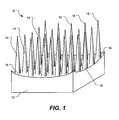
- FIG. 1is a perspective illustration of a micro-needle array having tips disposed along a non-planar surface in accordance with an embodiment of the present invention
- FIG. 2( a )- 2 ( f )is a series of illustrations of steps in fabricating a micro-needle array in accordance with an embodiment of the present invention, wherein FIG. 2( a ) is a side view illustration of a wafer, FIG. 2( b ) is a side view of the wafer after having a non-planar surface formed, FIG. 2( c ) is a side view of the wafer after having a plurality of trenches cut, FIG. 2( d ) is a top view of the wafer showing the tops of the plurality of columns, FIG. 2( e ) is a top view of the wafer after dynamic etching showing the columns have been rounded, and FIG. 2( f ) is a side view of the wafer showing the columns have been sharpened into micro-needles;
- FIG. 3is a side view illustration of a micro-needle array in accordance with another embodiment of the present invention.
- FIG. 4( a )- 4 ( d )is a series of illustrations of steps in fabricating a micro-needle array with insulating material between the micro-needles in accordance with an embodiment of the present invention, wherein FIG. 4( a ) is a side view of a wafer that has been sawed on the backside to form trenches, FIG. 4( b ) shows the wafer with the trenches filled with insulating material, FIG. 4( c ) shows the wafer after forming a non-planar surface on the front side and sawing a plurality of trenches into the front side; and FIG. 4( d ) shows the wafer after etching has formed the micro-needle array; and
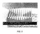
- FIG. 5is a scanning electron microscope picture of a micro-needle array having tips disposed in a convex non-planar surface in accordance with an embodiment of the present invention.
- a numerical range of “50-250 micrometersshould be interpreted to include not only the explicitly recited values of about 50 micrometers and 250 micrometers, but also include individual values and sub-ranges within the indicated range. Thus, included in this numerical range are individual values such as 60, 70, and 80 micrometers, and sub-ranges such as from 50-100 micrometers, from 100-200, and from 100-250 micrometers, etc. This same principle applies to ranges reciting only one numerical value and should apply regardless of the breadth of the range or the characteristics being described.
- the term “about”means that dimensions, sizes, formulations, parameters, shapes and other quantities and characteristics are not and need not be exact, but may be approximated and/or larger or smaller, as desired, reflecting tolerances, conversion factors, rounding off, measurement error and the like and other factors known to those of skill in the art. Further, unless otherwise stated, the term “about” shall expressly include “exactly,” consistent with the discussion above regarding ranges and numerical data.
- FIG. 1illustrates a perspective view of a micro-needle array in accordance with an embodiment of the present invention.
- the micro-needle array 10includes a substrate 12 and a plurality of spaced apart and substantially parallel micro-needles 14 .
- the micro-needleseach have a base 16 and a tip 18 , the bases of the micro-needles being supported by the substrate.
- the tips of the micro-needlesdefine a non-planar tip surface.
- the tips of the micro-needlesvary across and form a non-planar surface.
- This non-planar surfacecan be formed by micro-needles having varying heights or uniform height micro-needles distributed on a non-planar substrate surface.
- the tipsare arranged in a concave shaped surface, although other surface shapes can be provided as explained further below.
- the micro-needlesmay also include a conductive coating disposed on the tips of the micro-needles to help provide a low impedance electrical connection from the tissue in which the needle array is inserted to the needle body.
- the coatingmay be, for example, one or more metals, designed to adhere to and provide an Ohmic contact to the material used for the needle body and designed to provide a stable interface when inserted in vivo.
- silicon micro-needlesa metal stack of titanium over platinum over iridium has been found to provide good performance. The titanium adheres well to silicon, the platinum provides a diffusion barrier, and the iridium provides a stable electric interface when inserted in vivo.
- the micro-needle arraymay be encapsulated in a non-conductive, non-reactive material to help improve compatibility in vivo.
- a non-conductive, non-reactive materialcan include parylene-C, silicon carbide and/or silicone. It will be appreciated that the tips can be left unencapsulated to allow electric contact between the micro-needles and the tissue into which the array is inserted.
- the micro-needle arraycan be formed using various materials as will become more apparent from a discussion of fabrication techniques below.
- the micro-needles and the substratecan be formed from silicon.
- the micro-needlescan be formed of silicon or doped silicon and the substrate may be formed of glass.
- the substratemay be a plastic material. More particularly, the substrate may be a biodegradable plastic, such as polycaprolactone (PCL), poly (DL-lactide-co-glycolide) or polyglycolide.
- PCLpolycaprolactone
- the substratehelps to support the micro-needles during implantation. After implantation, the biodegradable plastic will dissolve, allowing the micro-needles to float in the tissue. This reduces mechanical coupling between the array and the tissue, helping to reduce neural damage.
- the tips 18can follow a concave surface, wherein tips near the center of the array are below tips near the edges of the array.
- the bases 16may define a similarly concave surface depressed into the substrate 12 , in which case the micro-needles 14 have similar lengths.
- the basesmay define a planar surface, in which case the micro-needles near the center of the array are shorter than micro-needles near the edges of the array.
- the tips 18can define a convex surface, where tips near the center of the array extend upward relative to tips near the edges of the array.
- the tips 18can be disposed in more complex surface shapes, having curvature in one dimension or two dimensions, depending on the number of sets of trenches that are cut.
- one set of saw cutscan define curvature in one dimension (direction).
- a second saw set of saw cutscan define curvature in a second dimension, producing a three-dimensional surface shape.
- the height (or depth) of the curved surface z relative to a horizontal referencee.g. the top surface of the wafer
- a function zf(x, y) of the horizontal position x, y.
- Achievable surface shapeswill be a function of the saw width, depth control (e.g., depth resolution), cutting angle control (e.g. vertical miter angle), rotational control of substrate (e.g. horizontal miter angle), etc.
- the micro-needles 14can be substantially parallel to each other. This can help to avoid tissue damage when the array is inserted into tissue, since lateral displacement of tissue by the micro-needles can be minimized by inserting the array into tissue in a direction aligned with the main axis of the micro-needles.
- a micro-needle array formed by bending a flexible substratemay result in needles which are not parallel to each other. Such an array is more likely to cause tissue damage upon insertion in some applications.
- micro-needles 14can be formed which are not parallel to each other as will become clear from the fabrication discussion below.
- the methodincludes providing a wafer 22 as shown in side view in FIG. 2( a ) from which the needle array is to be constructed.
- the wafercan be, for example, a mono-crystalline silicon wafer.
- Mono-crystalline silicon wafersare typically cut from a single crystal silicon ingot, for example as for integrated circuit manufacturing. It will be appreciated that the silicon wafer need not be perfectly single crystal, as most semiconductor grade silicon wafers contain a small number of defects of various types.
- Other wafer materials that can be usedinclude ceramic material and polymers.
- the methodfurther includes shaping a top surface of the wafer 22 into a non-planar surface 24 as shown FIG. 2( b ).
- the top surfacemay be shaped by gray scale lithography.
- a gray scale maskcreates three-dimensional structures within a photoresist layer than can be wet or dry etched to produce a curved surface.
- the non-planar surfacemay be formed by cutting a plurality of trenches of varying depth into the top surface, wherein the depth of the trenches corresponds to a non-planar surface and etching the top surface to remove material left between the trenches to form the non-planar surface as described in further detail below.
- the non-planar surfacemay be, for example, convex, concave, or other shapes.
- the non-planar surface 24is cut into to form a plurality of trenches 26 as shown in top view in FIG. 2( c ).
- Two sets of intersecting trenchesare cut to form a plurality of columns 27 having tops 28 defined by the non-planar surface.
- forming evenly spaced parallel saw cuts in one direction, turning the wafer 90 degrees, and forming a second set of evenly spaced parallel saw cutscan produce a plurality of square columns as shown in FIG. 2( d ).
- spacing between the saw cutscan be varied to produce rectangular columns and different size square columns.
- More than one set of saw cutscan be used, for example, using three sets of saw cuts at 60 degrees relative to each other to form triangular or hexagonal shaped columns.
- the cuttingcan be performed, for example, using a saw (e.g. a programmable dicing saw). Other techniques for cutting the trenches may also be used, including for example deep reactive ion etching.
- the methodalso includes etching the wafer to reshape the plurality of columns to round the columns and sharpen the tops into needle tips.
- etchingcan be performed using a dynamic etch to round the columns and a static etch to form points at the tips of the columns.
- Dynamic etchingcan be performed by placing the wafer into a holder and immersing the wafer in an etching solution.
- the holdercan be constructed of a material which is resistant to the etching solution, such as polytetrafluoroethylene (e.g. Teflon®) or other polymers.
- the holdercan include a gasket to help prevent contact between the back side of the wafer and the etching solution.
- the immersed waferis rotated in one direction, while a stirrer stirs the etching solution in an opposite direction to provide aggressive and continuous flow of fresh etching solution into the dicing kerfs.
- the size of the etching bathsize of the wafer
- concentration of the etching solutionconcentration of the etching solution
- total volume of the etching solutionsize of the stirring bar
- rotation rates of the wafer and stirrerand time of etching
- etching containerof 7.5 inch diameter, a stirring bar of 3 inches length, and 2 inches of separation between the stirrer bar and wafer
- rotating the wafer holder at about 22 rpm while counter rotating the stirrer bar at about 500 rpmprovided good uniformity of the etching of the columns.
- etching timeof about 4 minutes reduces 250 micrometer square columns to round column of about 150 micrometers in diameter.
- FIG. 2( e )after the dynamic etching, the columns have been reshaped to a plurality of rounded columns 27 ′ having substantially uniform cross section from base to tip, although there may be some narrowing of the columns toward the tip.
- Static etching to sharpen the tipscan be performed by inverting the holder to position the wafer columns in an upward direction and placing the wafer into etchant solution which is not stirred.
- the etching at the tips of the columnsis faster than near the bases, because little fluid motion is present to replenish etching solution near to bottoms of the kerfs.
- static etchingcan be performed for about 8 minutes. Longer etching tends to form more sharply pointed micro-needles, while shorter etching time tends to form more rounded, missile-shaped micro-needles.
- Etching timemay be in the range of about 2 to about 20 minutes, although in general longer etching times tend to decrease uniformity.
- the depth of the sawingcan be constant so that the bottom of the trenches 26 define a plane 36 .
- the bases 34 of the micro-needles 30are thus disposed within a plane 36 , and the micro-needles have varying length (height).
- the depth of the cuttingcan be varied so that the bases 34 of the columns 27 define a second non-planar surface 38 as shown in FIG. 3 .
- the depth of the cuttingcan be varied during forming of one set of parallel trenches to define a one-dimensional curve, or the depth can be varied during both sets of parallel trenches to define a two-dimensional curve. If the depth of the cutting follows the same profile as the (upper) non-planar surface 24 , the needles will have substantially the same height.
- the insulating materialcan be, for example, glass.
- a glass fritcan be disposed into the third set of trenches and then heating to melt and anneal the glass.
- a polymercan be reflowed into the trenches.
- biocompatible polymersuch as but not limited to benzo-cyclobutane (BCB)
- BCBcan be also be used as an insulating material between the electrodes.
- BCBcan be selectively patterned on the trenches using standard lithographic techniques (e.g. spin coating and curing).
- FIG. 4( a )- FIG. 4( d )illustrate a sequence of steps to provide the insulating material between the needles.
- the wafer 22is initially sawed on the backside 40 to form a third plurality of trenches 42 corresponding to the desired base surface 38 profile of the micro-needles.
- the sawingcan be fixed depth or variable depth, as for the front side.
- the trencheshave been filled with insulating material 44 .
- FIG. 4( c )the front surface has been formed into a non-planar shape and the first and second plurality of trenches 26 cut from the front side to intersect the insulating material.
- FIG. 5provides a scanning electron microscope image of an electrode array having a concave non-planar tip surface.
- non-planar surfacescan be formed by cutting trenches of varying depth into the surface of the wafer.
- the trenchesdefine a non-planar or curved profile.
- the cuttingcan be performed mechanically, for example, using a dicing saw, leaving residual material between the trenches.
- the residual materialcan be removed using an isotropic etching to form the desired non-planar smooth surface.
- siliconcan be etched using a solution of hydrofluoric acid, as well as other known etchants.
- a mixture of hydrofluoric acid, nitric acid, acetic acid (HNA), and wateris a useful etchant.
- the curved surfacecorresponds to the a desired surface profile, but may be displaced somewhat deeper into the wafer, since etching also removes some material from the substrate at the bottom of the trenches.
- More than one plurality of trenchesmay be cut into the substrate to define a more complex profile. Just as one, two, three, or even more sets of trenches may be cut into the top-side to define complex non-planar surface profiles for the bases of the micro-needles, the same operations can be performed to define a non-planar surface profile for the tips of the micro-needles. Note that the profiles for the tips and bases need not be the same, although some variation in etching rate of the micro-needles may result under such conditions.
- trenchesare cut perpendicularly to the surface of the wafer being cut, this is not essential. If desired, trenches may be cut at an angle relative to vertical. Some non-planar surface profiles may be more efficiently fabricating by using a combination of angled cuts. It will also be appreciated that by using angled cuts, the columns formed need not be parallel, and accordingly can result in an array of needles that are not parallel to each other.
- U.S. Provisional Patent Application Ser. No. 60/932,232entitled “MICRO-LENS ARRAYS AND CURVED SURFACE FABRICATION TECHNIQUES”, provides additional detail on a method for forming curved surfaces.
- Various coatingsmay be applied to the micro-needles arrays.
- metal coatingscan be applied to the tips of the micro-needles to reduce the interconnect impedance between the micro-needle and tissue into which the micro-needle array is inserted.
- Biocompatible coatingssuch as parylene-C and/or silicon carbide can be coated over the array.
- tipsmay be metallized, the array encapsulated in parylene-C, and then the tips of the array de-encapsulation to expose the tips.
- De-encapsulationmay be performed using various techniques, including for example, shadow masking and laser ablation, plasma etching using masking techniques as disclosed in U.S. patent application Ser. No. 11/807,763, entitled “MASKING HIGH ASPECT-RATIO STRUCTURES”, and other techniques as known in the art.
- a non-planar micro-electrode arraycan also be fabricated using a molding process using a micro-electrode array as fabricated above as a master.
- a polymer moldcan be created from the non-planar micro-needle array by pouring polymer material on the micro-electrode array and curing the polymer material which takes on the inverted shape of the micro-needle array.
- the moldcan be used to produce additional arrays, for example, by filling the mold with polymer material and curing, or electroplating metal onto the mold.
- Various polymersmay be suitable for use in such an application, including for example poly-dimethy-siloxane (PDMS), polyesters, poly-tetra-fluoroethylene (PTFE), the SU-8 photo resist, and similar materials.
- An optional release agentcan be used on the mold to facilitate release of molded arrays from the mold after forming is complete.
- a pre-arraycan be formed which is approximately the shape of a desired non-planar micro-electrode array, but which requires further processing subsequent to molding. For example, at least a portion of dynamic and/or static etching steps can be performed subsequent to molding such that the pre-array may appear less rounded than typical final micro-needles. In this manner, more robust features can be molded with reduced likelihood of fracture during removal from the molds. The robust features can then be etched to from the desired micro-needle array.
- micro-needle arrays having tips disposed in a non-planar surfacehave been described.
- the non-planar surfacecan be form specifically fitted for peripheral nerves, auditory nerves, retinal surfaces, etc. This enables the implanted micro-needle array to be secured around the nerve or surface and thus physically stabilized against displacement. This can help to avoid needing to seal the array to a nerve trunk (e.g. with sutures) helping to reduce neural damage.
- electrode heightscan be optimized to create localized electrical fields, making possible better selectivity in activating specific nerve regions.
Landscapes
- Health & Medical Sciences (AREA)
- Engineering & Computer Science (AREA)
- Dermatology (AREA)
- Medical Informatics (AREA)
- Anesthesiology (AREA)
- Biomedical Technology (AREA)
- Heart & Thoracic Surgery (AREA)
- Hematology (AREA)
- Life Sciences & Earth Sciences (AREA)
- Animal Behavior & Ethology (AREA)
- General Health & Medical Sciences (AREA)
- Public Health (AREA)
- Veterinary Medicine (AREA)
- Micromachines (AREA)
- Infusion, Injection, And Reservoir Apparatuses (AREA)
Abstract
Description
Claims (23)
Priority Applications (2)
| Application Number | Priority Date | Filing Date | Title |
|---|---|---|---|
| US11/807,766US8865288B2 (en) | 2006-07-17 | 2007-05-29 | Micro-needle arrays having non-planar tips and methods of manufacture thereof |
| PCT/US2008/065169WO2009014805A2 (en) | 2007-05-29 | 2008-05-29 | Micro-needle arrays having non-planar tips and methods of manufacture thereof |
Applications Claiming Priority (2)
| Application Number | Priority Date | Filing Date | Title |
|---|---|---|---|
| US83155706P | 2006-07-17 | 2006-07-17 | |
| US11/807,766US8865288B2 (en) | 2006-07-17 | 2007-05-29 | Micro-needle arrays having non-planar tips and methods of manufacture thereof |
Publications (2)
| Publication Number | Publication Date |
|---|---|
| US20080138583A1 US20080138583A1 (en) | 2008-06-12 |
| US8865288B2true US8865288B2 (en) | 2014-10-21 |
Family
ID=40282060
Family Applications (1)
| Application Number | Title | Priority Date | Filing Date |
|---|---|---|---|
| US11/807,766Active2027-10-23US8865288B2 (en) | 2006-07-17 | 2007-05-29 | Micro-needle arrays having non-planar tips and methods of manufacture thereof |
Country Status (2)
| Country | Link |
|---|---|
| US (1) | US8865288B2 (en) |
| WO (1) | WO2009014805A2 (en) |
Cited By (16)
| Publication number | Priority date | Publication date | Assignee | Title |
|---|---|---|---|---|
| US20140323811A1 (en)* | 2013-04-30 | 2014-10-30 | Invuity, Inc. | Methods and apparatus for retracting tissue |
| US9923008B2 (en)* | 2013-04-12 | 2018-03-20 | Omnivision Technologies, Inc. | Wafer-level array cameras and methods for fabricating the same |
| US20180113242A1 (en)* | 2016-10-24 | 2018-04-26 | Samsung Electronics Co., Ltd. | Pattern structure and method of manufacturing the pattern structure |
| US9986988B2 (en) | 2014-11-27 | 2018-06-05 | AOD Holdings, LLC | Surgical retractor |
| US10376168B1 (en)* | 2013-03-14 | 2019-08-13 | Orbital Research Inc. | Dry physiological recording device and method of manufacturing |
| US10549099B2 (en) | 2016-04-29 | 2020-02-04 | University Of Utah Research Foundation | Electronic peripheral nerve stimulation |
| US10980448B2 (en) | 2018-05-16 | 2021-04-20 | International Business Machines Corporation | Electrically functional polymer microneedle array |
| US11123532B2 (en) | 2013-03-14 | 2021-09-21 | One Drop Biosensor Technologies, Llc | On-body microsensor for biomonitoring |
| US11172851B2 (en) | 2014-03-13 | 2021-11-16 | One Drop Biosensor Technologies, Llc | System for monitoring body chemistry |
| US11272866B2 (en) | 2014-03-13 | 2022-03-15 | One Drop Biosensor Technologies, Llc | Wearable microneedle patch |
| US11272885B2 (en) | 2013-03-14 | 2022-03-15 | One Drop Biosensor Technologies, Llc | Wearable multi-analyte microsensor |
| US11547849B2 (en) | 2017-06-07 | 2023-01-10 | Neuronexus Technologies, Inc. | Systems and methods for ruggedized penetrating medical electrode arrays |
| USD988882S1 (en) | 2021-04-21 | 2023-06-13 | Informed Data Systems Inc. | Sensor assembly |
| US11846882B2 (en) | 2020-01-31 | 2023-12-19 | Korea Institute Of Science And Technology | Methods for manufacturing high-density neural probes having various forms |
| USD1076079S1 (en) | 2021-04-21 | 2025-05-20 | One Health Biosensing Inc. | Applicator assembly |
| USD1086030S1 (en) | 2021-04-21 | 2025-07-29 | One Health Biosensing Inc. | Charging station |
Families Citing this family (36)
| Publication number | Priority date | Publication date | Assignee | Title |
|---|---|---|---|---|
| US7591618B2 (en)* | 2004-02-25 | 2009-09-22 | Agency For Science, Technology And Research | Machining method for micro abraders and micro abraders produced thereby |
| US7942827B2 (en)* | 2005-07-11 | 2011-05-17 | Infotonics Technology Center, Inc. | Minimally invasive allergy testing system |
| US20080138581A1 (en)* | 2006-07-17 | 2008-06-12 | Rajmohan Bhandari | Masking high-aspect aspect ratio structures |
| US7777956B2 (en)* | 2007-05-29 | 2010-08-17 | University Of Utah Research Foundation | Micro-lens arrays and curved surface fabrication techniques |
| US20100010601A1 (en)* | 2008-01-07 | 2010-01-14 | Sandeep Negi | Self-Aligning Latch-up Mechanism in Out of Plane Silicon Microelectrode Arrays |
| US8359083B2 (en)* | 2008-04-02 | 2013-01-22 | University Of Utah Research Foundation | Microelectrode array system with integrated reference microelectrodes to reduce detected electrical noise and improve selectivity of activation |
| US20090301994A1 (en)* | 2008-05-12 | 2009-12-10 | Rajmohan Bhandari | Methods for Wafer Scale Processing of Needle Array Devices |
| ES2687258T3 (en)* | 2008-05-21 | 2018-10-24 | Theraject, Inc. | Manufacturing procedure of microneedle assemblies |
| US8886279B2 (en) | 2008-06-03 | 2014-11-11 | University Of Utah Research Foundation | High aspect ratio microelectrode arrays enabled to have customizable lengths and methods of making the same |
| JP5284014B2 (en)* | 2008-09-02 | 2013-09-11 | 株式会社ニデック | Visual reproduction assist device |
| JP5284027B2 (en)* | 2008-09-30 | 2013-09-11 | 株式会社ニデック | Visual reproduction assist device |
| US8639312B2 (en)* | 2008-12-10 | 2014-01-28 | University Of Utah Research Foundation | System and method for electrically shielding a microelectrode array in a physiological pathway from electrical noise |
| CN101829396B (en)* | 2009-03-27 | 2013-01-30 | 清华大学 | Microneedle array chip, transdermal drug delivery patch using same and preparation method thereof |
| CN101829395B (en)* | 2010-05-20 | 2012-08-22 | 上海交通大学 | Method for preparing solid micro-needle array in cutting way |
| US20130158482A1 (en)* | 2010-07-26 | 2013-06-20 | Seventh Sense Biosystems, Inc. | Rapid delivery and/or receiving of fluids |
| WO2012064802A1 (en) | 2010-11-09 | 2012-05-18 | Seventh Sense Biosystems, Inc. | Systems and interfaces for blood sampling |
| KR101241336B1 (en)* | 2010-12-30 | 2013-03-11 | 광주과학기술원 | Microelectrode Array and Fabrication Method thereof |
| JP2014097163A (en)* | 2012-11-14 | 2014-05-29 | Ikeda Kikai Sangyo Kk | Method of manufacturing microneedle array |
| US9700221B2 (en) | 2013-03-06 | 2017-07-11 | Axion Biosystems, Inc. | Non-invasive segmentable three-dimensional microelectrode array patch for neurophysiological diagnostics and therapeutic stimulation |
| GB2536163B (en)* | 2013-10-17 | 2017-11-15 | Monica Healthcare Ltd | Apparatus and method for detecting an abdominal electrophysiological signal |
| US10959631B2 (en) | 2014-02-01 | 2021-03-30 | Biocircuit Technologies, Inc. | Neural interfacing device |
| US9138191B1 (en) | 2014-07-09 | 2015-09-22 | Qualcomm Incorporated | Integrated circuit module with lead frame micro-needles |
| JP5967595B2 (en)* | 2014-09-08 | 2016-08-10 | 株式会社かいわ | Puncture device |
| WO2016039333A1 (en)* | 2014-09-08 | 2016-03-17 | 株式会社かいわ | Puncture device |
| CN104398258B (en)* | 2014-11-03 | 2016-05-25 | 中国科学院深圳先进技术研究院 | 3D fibril electrode array fixture and 3D fibril electrode array method of cutting out |
| JP6317690B2 (en) | 2015-03-03 | 2018-04-25 | 富士フイルム株式会社 | Transdermal absorption sheet and method for producing the same |
| JP6482323B2 (en) | 2015-03-03 | 2019-03-13 | 富士フイルム株式会社 | Transdermal absorption sheet |
| US11298039B2 (en)* | 2015-04-17 | 2022-04-12 | Samsung Electronics Co., Ltd | Biometric information measuring sensor, biometric information measuring system, and method of measuring biometric information using the sensor |
| CN105615874A (en)* | 2016-03-01 | 2016-06-01 | 中国科学院半导体研究所 | Flexible electrocardio-electrode for dynamic electrocardiograph measurement and manufacturing method of flexible electrocardio-electrode for dynamic electrocardiograph measurement |
| ES3037878T3 (en) | 2016-09-06 | 2025-10-07 | Biocircuit Tech Inc | Devices for repairing damage to a nerve |
| CN106835011B (en)* | 2016-12-20 | 2019-06-25 | 深圳先进技术研究院 | A kind of structural member and preparation method thereof with diamond-like array |
| CA3058920A1 (en)* | 2017-04-04 | 2018-10-11 | Neuraura Biotech Inc. | Apparatus and method for capturing neural recordings |
| CN108975266B (en)* | 2018-07-17 | 2020-11-10 | 中北大学 | Graphene-PDMS flexible substrate ECG dry electrode based on needle-tip array structure and preparation method thereof |
| US11744501B2 (en) | 2020-05-07 | 2023-09-05 | GE Precision Healthcare LLC | Multi-sensor patch |
| TWI741732B (en)* | 2020-08-12 | 2021-10-01 | 淡江大學學校財團法人淡江大學 | Method for manufacturing micro-needle device |
| TWI851159B (en)* | 2023-04-20 | 2024-08-01 | 達運精密工業股份有限公司 | Microneedle patch and manufacturing method thereof |
Citations (58)
| Publication number | Priority date | Publication date | Assignee | Title |
|---|---|---|---|---|
| US4685466A (en) | 1985-01-29 | 1987-08-11 | Rau Guenter | Measuring sensor for the non-invasive detection of electro-physiological quantities |
| US4837049A (en) | 1986-06-17 | 1989-06-06 | Alfred E. Mann Foundation For Scientific Research | Method of making an electrode array |
| US4969468A (en) | 1986-06-17 | 1990-11-13 | Alfred E. Mann Foundation For Scientific Research | Electrode array for use in connection with a living body and method of manufacture |
| US5215088A (en) | 1989-11-07 | 1993-06-01 | The University Of Utah | Three-dimensional electrode device |
| US5286944A (en) | 1992-03-25 | 1994-02-15 | Panasonic Technologies, Inc. | Method of manufacturing a multiple microelectrode assembly |
| US5388577A (en) | 1990-06-08 | 1995-02-14 | Boston University | Electrode array microchip |
| US5457041A (en) | 1994-03-25 | 1995-10-10 | Science Applications International Corporation | Needle array and method of introducing biological substances into living cells using the needle array |
| US5472592A (en) | 1994-07-19 | 1995-12-05 | American Plating Systems | Electrolytic plating apparatus and method |
| US5656414A (en) | 1993-04-23 | 1997-08-12 | Fujitsu Limited | Methods of forming tall, high-aspect ratio vias and trenches in photo-imageable materials, photoresist materials, and the like |
| US5689603A (en) | 1993-07-07 | 1997-11-18 | Huth; Gerald C. | Optically interactive nanostructure |
| US5838715A (en) | 1996-06-20 | 1998-11-17 | Hewlett-Packard Company | High intensity single-mode VCSELs |
| US5895562A (en) | 1997-06-19 | 1999-04-20 | Advanced Micro Devices, Inc. | Gas shielding during plating |
| US6091975A (en) | 1998-04-01 | 2000-07-18 | Alza Corporation | Minimally invasive detecting device |
| US6285446B1 (en) | 1997-05-19 | 2001-09-04 | Sensornet Limited | Distributed sensing system |
| US6334856B1 (en) | 1998-06-10 | 2002-01-01 | Georgia Tech Research Corporation | Microneedle devices and methods of manufacture and use thereof |
| US6406638B1 (en) | 2000-01-06 | 2002-06-18 | The Regents Of The University Of California | Method of forming vertical, hollow needles within a semiconductor substrate, and needles formed thereby |
| US20020082543A1 (en) | 2000-12-14 | 2002-06-27 | Jung-Hwan Park | Microneedle devices and production thereof |
| US6511463B1 (en) | 1999-11-18 | 2003-01-28 | Jds Uniphase Corporation | Methods of fabricating microneedle arrays using sacrificial molds |
| US6551849B1 (en)* | 1999-11-02 | 2003-04-22 | Christopher J. Kenney | Method for fabricating arrays of micro-needles |
| US6622035B1 (en) | 2000-01-21 | 2003-09-16 | Instrumentarium Corp. | Electrode for measurement of weak bioelectrical signals |
| US20030208138A1 (en) | 2001-07-09 | 2003-11-06 | Lorin Olson | Micro-needles and methods of manufacture and use thereof |
| US6702950B2 (en) | 1999-06-16 | 2004-03-09 | James E. Moon | Method for fabricating LC device using latent masking and delayed LOCOS techniques |
| US20040048419A1 (en) | 2001-11-30 | 2004-03-11 | Masahiko Kitamura | Production method for semiconductor chip |
| US20040082875A1 (en) | 2002-10-24 | 2004-04-29 | Brown University Research Foundation | Microstructured arrays for cortex interaction and related methods of manufacture and use |
| US6730444B2 (en) | 2001-06-05 | 2004-05-04 | Micron Technology, Inc. | Needle comb reticle pattern for critical dimension and registration measurements using a registration tool and methods for using same |
| US6743211B1 (en)* | 1999-11-23 | 2004-06-01 | Georgia Tech Research Corporation | Devices and methods for enhanced microneedle penetration of biological barriers |
| US6782283B2 (en) | 2001-09-07 | 2004-08-24 | Robert N. Schmidt | Dry penetrating recording device |
| US6815360B1 (en) | 1998-07-22 | 2004-11-09 | Qinetiq Limited | Silicon micro-machined projection with duct |
| US20040267205A1 (en) | 2001-08-14 | 2004-12-30 | Goran Stemme | Micro needles and method of manufacture thereof |
| US20050011858A1 (en) | 2003-07-16 | 2005-01-20 | Industrial Technology Research Institute | Method for fabricating a hollow micro-needle array |
| US6896850B2 (en) | 2001-03-26 | 2005-05-24 | Kumetrix, Inc. | Silicon nitride window for microsampling device and method of construction |
| US20050171480A1 (en) | 2003-11-21 | 2005-08-04 | The Regents Of The University Of California | Method and/or apparatus for puncturing a surface for extraction, in situ analysis, and/or substance delivery using microneedles |
| WO2005072630A1 (en) | 2004-01-30 | 2005-08-11 | Isis Innovation Limited | Device for delivery of bioactive materials and other stimuli |
| US20050258514A1 (en)* | 2004-05-07 | 2005-11-24 | Stillwater Scientific | Microfabricated miniature grids |
| US6980282B2 (en) | 2002-12-11 | 2005-12-27 | Molecular Imprints, Inc. | Method for modulating shapes of substrates |
| US20060055090A1 (en) | 2003-01-16 | 2006-03-16 | Lee Seung-Seob | Method for manufacturing of polymer micro needle array with liga process |
| US7027874B1 (en) | 2000-11-16 | 2006-04-11 | Polyvalor S.E.C. | Body electronic implant and artificial vision system thereof |
| US20060110100A1 (en) | 2003-01-24 | 2006-05-25 | Blauvelt Henry A | Etched-facet semiconductor optical component with integrated end-coupled waveguide and methods of fabrication and use thereof |
| WO2006055799A1 (en) | 2004-11-18 | 2006-05-26 | 3M Innovative Properties Company | Masking method for coating a microneedle array |
| US20060127307A1 (en) | 2003-01-31 | 2006-06-15 | Canham Leight T | Devices and compositions containing boron and silicon for use in neutron capture therapy |
| US20060135862A1 (en) | 2003-06-12 | 2006-06-22 | Tootle John S | Multielectrode array and system for recording and analyzing data or for stimulating tissue |
| US20060173259A1 (en) | 2004-10-04 | 2006-08-03 | Flaherty J C | Biological interface system |
| US7118942B1 (en) | 2000-09-27 | 2006-10-10 | Li Chou H | Method of making atomic integrated circuit device |
| US20070067007A1 (en) | 2005-05-25 | 2007-03-22 | Alfred E. Mann Foundation For Scientific Research | Hermetically sealed three-dimensional electrode array |
| US7240416B2 (en) | 2001-05-07 | 2007-07-10 | Cochlear Limited | Process for manufacturing electrically conductive components |
| US20070161964A1 (en) | 2006-01-10 | 2007-07-12 | Yuzhakov Vadim V | Microneedle array, patch, and applicator for transdermal drug delivery |
| US20080125743A1 (en) | 2006-11-28 | 2008-05-29 | Yuzhakov Vadim V | Tissue Conforming Microneedle Array and Patch For Transdermal Drug Delivery or Biological Fluid Collection |
| US20080138581A1 (en) | 2006-07-17 | 2008-06-12 | Rajmohan Bhandari | Masking high-aspect aspect ratio structures |
| US20080138582A1 (en) | 2006-07-17 | 2008-06-12 | Rajmohan Bhandari | Water-scale needle array |
| US20080262416A1 (en) | 2005-11-18 | 2008-10-23 | Duan Daniel C | Microneedle Arrays and Methods of Preparing Same |
| US20080275400A1 (en) | 2005-12-23 | 2008-11-06 | Ferguson Dennis E | Manufacturing Microneedle Arrays |
| US20090011158A1 (en) | 2007-03-18 | 2009-01-08 | Nanopass Technologies Ltd. | Microneedle structures and corresponding production methods employing a backside wet etch |
| US20090099534A1 (en) | 2006-07-12 | 2009-04-16 | University Of Utah Research Foundation | 3D fabrication of needle tip geometry and knife blade |
| US20090283425A1 (en) | 2008-04-02 | 2009-11-19 | University Of Utah Research Foundation | Microelectrode Array System With Integrated Reference Microelectrodes To Reduce Detected Electrical Noise And Improve Selectivity Of Activation |
| US20090301994A1 (en) | 2008-05-12 | 2009-12-10 | Rajmohan Bhandari | Methods for Wafer Scale Processing of Needle Array Devices |
| US20100041972A1 (en) | 2006-07-07 | 2010-02-18 | Lectus Therapeutics Limited | Apparatus and methods |
| US7712198B2 (en) | 2004-07-16 | 2010-05-11 | Industrial Technology Research Institute | Microneedle array device and its fabrication method |
| US7991475B1 (en) | 2005-06-08 | 2011-08-02 | The Regents Of The University Of California | High density micromachined electrode arrays useable for auditory nerve implants and related methods |
- 2007
- 2007-05-29USUS11/807,766patent/US8865288B2/enactiveActive
- 2008
- 2008-05-29WOPCT/US2008/065169patent/WO2009014805A2/enactiveApplication Filing
Patent Citations (63)
| Publication number | Priority date | Publication date | Assignee | Title |
|---|---|---|---|---|
| US4685466A (en) | 1985-01-29 | 1987-08-11 | Rau Guenter | Measuring sensor for the non-invasive detection of electro-physiological quantities |
| US4837049A (en) | 1986-06-17 | 1989-06-06 | Alfred E. Mann Foundation For Scientific Research | Method of making an electrode array |
| US4969468A (en) | 1986-06-17 | 1990-11-13 | Alfred E. Mann Foundation For Scientific Research | Electrode array for use in connection with a living body and method of manufacture |
| US5215088A (en) | 1989-11-07 | 1993-06-01 | The University Of Utah | Three-dimensional electrode device |
| US5388577A (en) | 1990-06-08 | 1995-02-14 | Boston University | Electrode array microchip |
| US5286944A (en) | 1992-03-25 | 1994-02-15 | Panasonic Technologies, Inc. | Method of manufacturing a multiple microelectrode assembly |
| US5656414A (en) | 1993-04-23 | 1997-08-12 | Fujitsu Limited | Methods of forming tall, high-aspect ratio vias and trenches in photo-imageable materials, photoresist materials, and the like |
| US5689603A (en) | 1993-07-07 | 1997-11-18 | Huth; Gerald C. | Optically interactive nanostructure |
| US5457041A (en) | 1994-03-25 | 1995-10-10 | Science Applications International Corporation | Needle array and method of introducing biological substances into living cells using the needle array |
| US5472592A (en) | 1994-07-19 | 1995-12-05 | American Plating Systems | Electrolytic plating apparatus and method |
| US5838715A (en) | 1996-06-20 | 1998-11-17 | Hewlett-Packard Company | High intensity single-mode VCSELs |
| US6285446B1 (en) | 1997-05-19 | 2001-09-04 | Sensornet Limited | Distributed sensing system |
| US5895562A (en) | 1997-06-19 | 1999-04-20 | Advanced Micro Devices, Inc. | Gas shielding during plating |
| US6091975A (en) | 1998-04-01 | 2000-07-18 | Alza Corporation | Minimally invasive detecting device |
| US6334856B1 (en) | 1998-06-10 | 2002-01-01 | Georgia Tech Research Corporation | Microneedle devices and methods of manufacture and use thereof |
| US6815360B1 (en) | 1998-07-22 | 2004-11-09 | Qinetiq Limited | Silicon micro-machined projection with duct |
| US6702950B2 (en) | 1999-06-16 | 2004-03-09 | James E. Moon | Method for fabricating LC device using latent masking and delayed LOCOS techniques |
| US6551849B1 (en)* | 1999-11-02 | 2003-04-22 | Christopher J. Kenney | Method for fabricating arrays of micro-needles |
| US7332197B2 (en) | 1999-11-18 | 2008-02-19 | Memscap S.A. | Methods of fabricating microneedle arrays using sacrificial molds, and microneedle arrays fabricated thereby |
| US6511463B1 (en) | 1999-11-18 | 2003-01-28 | Jds Uniphase Corporation | Methods of fabricating microneedle arrays using sacrificial molds |
| US20050137531A1 (en) | 1999-11-23 | 2005-06-23 | Prausnitz Mark R. | Devices and methods for enhanced microneedle penetration of biological barriers |
| US6743211B1 (en)* | 1999-11-23 | 2004-06-01 | Georgia Tech Research Corporation | Devices and methods for enhanced microneedle penetration of biological barriers |
| US6406638B1 (en) | 2000-01-06 | 2002-06-18 | The Regents Of The University Of California | Method of forming vertical, hollow needles within a semiconductor substrate, and needles formed thereby |
| US6622035B1 (en) | 2000-01-21 | 2003-09-16 | Instrumentarium Corp. | Electrode for measurement of weak bioelectrical signals |
| US7118942B1 (en) | 2000-09-27 | 2006-10-10 | Li Chou H | Method of making atomic integrated circuit device |
| US7027874B1 (en) | 2000-11-16 | 2006-04-11 | Polyvalor S.E.C. | Body electronic implant and artificial vision system thereof |
| US20020082543A1 (en) | 2000-12-14 | 2002-06-27 | Jung-Hwan Park | Microneedle devices and production thereof |
| US6896850B2 (en) | 2001-03-26 | 2005-05-24 | Kumetrix, Inc. | Silicon nitride window for microsampling device and method of construction |
| US7240416B2 (en) | 2001-05-07 | 2007-07-10 | Cochlear Limited | Process for manufacturing electrically conductive components |
| US6730444B2 (en) | 2001-06-05 | 2004-05-04 | Micron Technology, Inc. | Needle comb reticle pattern for critical dimension and registration measurements using a registration tool and methods for using same |
| US20030208138A1 (en) | 2001-07-09 | 2003-11-06 | Lorin Olson | Micro-needles and methods of manufacture and use thereof |
| US20040267205A1 (en) | 2001-08-14 | 2004-12-30 | Goran Stemme | Micro needles and method of manufacture thereof |
| US6782283B2 (en) | 2001-09-07 | 2004-08-24 | Robert N. Schmidt | Dry penetrating recording device |
| US20040048419A1 (en) | 2001-11-30 | 2004-03-11 | Masahiko Kitamura | Production method for semiconductor chip |
| US7212851B2 (en) | 2002-10-24 | 2007-05-01 | Brown University Research Foundation | Microstructured arrays for cortex interaction and related methods of manufacture and use |
| US20040082875A1 (en) | 2002-10-24 | 2004-04-29 | Brown University Research Foundation | Microstructured arrays for cortex interaction and related methods of manufacture and use |
| US6980282B2 (en) | 2002-12-11 | 2005-12-27 | Molecular Imprints, Inc. | Method for modulating shapes of substrates |
| US20060055090A1 (en) | 2003-01-16 | 2006-03-16 | Lee Seung-Seob | Method for manufacturing of polymer micro needle array with liga process |
| US20060110100A1 (en) | 2003-01-24 | 2006-05-25 | Blauvelt Henry A | Etched-facet semiconductor optical component with integrated end-coupled waveguide and methods of fabrication and use thereof |
| US20060127307A1 (en) | 2003-01-31 | 2006-06-15 | Canham Leight T | Devices and compositions containing boron and silicon for use in neutron capture therapy |
| US20060135862A1 (en) | 2003-06-12 | 2006-06-22 | Tootle John S | Multielectrode array and system for recording and analyzing data or for stimulating tissue |
| US20050011858A1 (en) | 2003-07-16 | 2005-01-20 | Industrial Technology Research Institute | Method for fabricating a hollow micro-needle array |
| US20050171480A1 (en) | 2003-11-21 | 2005-08-04 | The Regents Of The University Of California | Method and/or apparatus for puncturing a surface for extraction, in situ analysis, and/or substance delivery using microneedles |
| WO2005072630A1 (en) | 2004-01-30 | 2005-08-11 | Isis Innovation Limited | Device for delivery of bioactive materials and other stimuli |
| US20050258514A1 (en)* | 2004-05-07 | 2005-11-24 | Stillwater Scientific | Microfabricated miniature grids |
| US7712198B2 (en) | 2004-07-16 | 2010-05-11 | Industrial Technology Research Institute | Microneedle array device and its fabrication method |
| US20060173259A1 (en) | 2004-10-04 | 2006-08-03 | Flaherty J C | Biological interface system |
| WO2006055799A1 (en) | 2004-11-18 | 2006-05-26 | 3M Innovative Properties Company | Masking method for coating a microneedle array |
| US20080102192A1 (en) | 2004-11-18 | 2008-05-01 | Johnson Peter R | Masking Method for Coating a Microneedle Array |
| US20070067007A1 (en) | 2005-05-25 | 2007-03-22 | Alfred E. Mann Foundation For Scientific Research | Hermetically sealed three-dimensional electrode array |
| US7991475B1 (en) | 2005-06-08 | 2011-08-02 | The Regents Of The University Of California | High density micromachined electrode arrays useable for auditory nerve implants and related methods |
| US20080262416A1 (en) | 2005-11-18 | 2008-10-23 | Duan Daniel C | Microneedle Arrays and Methods of Preparing Same |
| US20080275400A1 (en) | 2005-12-23 | 2008-11-06 | Ferguson Dennis E | Manufacturing Microneedle Arrays |
| US20070161964A1 (en) | 2006-01-10 | 2007-07-12 | Yuzhakov Vadim V | Microneedle array, patch, and applicator for transdermal drug delivery |
| US20100041972A1 (en) | 2006-07-07 | 2010-02-18 | Lectus Therapeutics Limited | Apparatus and methods |
| US20090099534A1 (en) | 2006-07-12 | 2009-04-16 | University Of Utah Research Foundation | 3D fabrication of needle tip geometry and knife blade |
| US20080138582A1 (en) | 2006-07-17 | 2008-06-12 | Rajmohan Bhandari | Water-scale needle array |
| US7951300B2 (en) | 2006-07-17 | 2011-05-31 | University Of Utah Research Foundation | Water-scale needle array |
| US20080138581A1 (en) | 2006-07-17 | 2008-06-12 | Rajmohan Bhandari | Masking high-aspect aspect ratio structures |
| US20080125743A1 (en) | 2006-11-28 | 2008-05-29 | Yuzhakov Vadim V | Tissue Conforming Microneedle Array and Patch For Transdermal Drug Delivery or Biological Fluid Collection |
| US20090011158A1 (en) | 2007-03-18 | 2009-01-08 | Nanopass Technologies Ltd. | Microneedle structures and corresponding production methods employing a backside wet etch |
| US20090283425A1 (en) | 2008-04-02 | 2009-11-19 | University Of Utah Research Foundation | Microelectrode Array System With Integrated Reference Microelectrodes To Reduce Detected Electrical Noise And Improve Selectivity Of Activation |
| US20090301994A1 (en) | 2008-05-12 | 2009-12-10 | Rajmohan Bhandari | Methods for Wafer Scale Processing of Needle Array Devices |
Non-Patent Citations (18)
| Title |
|---|
| Bhandari et al; A Novel Method of Fabrication Covoluted Shaped Electrode Arrays for Neural and Retinal Prostheses; Sensors and Actuators A; Nov. 4, 2007; pp. 123-130; vol. 145-146. |
| Branner et al; Long Term Stimulation and Recording with a Penetration Microelectrode Array in Cat Sciatic Nerve; IEEE Transactions on Biomedical Engineering; vol. 51, No. 1; Jan. 2004. |
| Campbell et al.; A Silicon-Based, Three Dimensional Neural Interface: Manufacturing Process for an Intracortical Electrode Array; IEEE; Aug. 1991; pp. 758-768; vol. 38, No. 8. |
| Clark et al.; DARPA Revolutionizing Prosthetics 2009; Making It Work: Animal Physiology & Device Testing; Dept. of Bioengineering University of Utah Jun. 28, 2007; 5 pgs. |
| Dhillon et al.; Residual Function in Peripheral Nerve Stumps of Amputees: Implications for Neural Control of Artificial Limbs; The Journal of Hand Surgery; 2004; pp. 605-615. |
| Fofonoff, T. et al. A highly flexible manufacturing technique for microelectrode array fabrication In: [Engineering in Medicine and Biology, 2002. 24th Annual Conference and the Annual Fall Meeting of the Biomedical Engineering Society] EMBS/BMES Conference, 2002, pp. 2107-2108. |
| Fofonoff, T. et al. Assembly-ready brain microelectrode array's In: Engineering in Medicine and Biology Society, Proceedings of the 25th Annual International Conference of the IEEE, 2003, pp. 1937-1940. |
| Jones, Kelly et al. "A glass/silicon composite intracortical electrode array", Annals of Biomedical Engineering, 1992, pp. 423-437, vol. 20.* |
| Rakwal et al; Fabrication of Compliant High Aspect Ratio Silicon Microelectrode Arrays Using Micro-Wire Electrical Discharge Machining; Microsyst Technol; 2009; pp. 789-797; vol. 15. |
| Tajadod et al.; Electophoretic Photoresist Application for High Topography Wafer Surfaces; International Conference on Compound Semiconductor Mfg; 2003; 4 pgs. |
| Tathireddy et al; Fabrication of 3-Dimensional Silicon Microelectrode Arrays Using Micro Electro Discharge Machining for Neural Applications; Proc. Transducer'09, 15th Int. Conf. on Solid-State Sensors, Actuators and Microsystems, Denver, CO, Jun. 21-25, 2009, pp. 1206-1209. |
| Tathireddy et al; Towards High Aspect Ratio Tungsten Micro Electrode Array for Neural Recording and Stimulation Applications; 13th Annual International Function Electrical Stimulation (FES) Society Conference, Freiburg, Germany, Sep. 21-25, 2008. |
| Tsung-Kuan et al. "Fabrication of Out-of-Plane Curved surfaces in Si by Utilizing Rie Lag," IEEE, 2002, pp. 145-148. |
| U.S. Appl. No. 11/807,766, filed May 29, 2007; Rajmohan Bhandari; office action dated Feb. 19, 2013. |
| U.S. Appl. No. 12/464,691, filed May 12, 2009; Rajmohan Bhandari; office action dated Feb. 7, 2013. |
| U.S. Appl. No. 12/464,691, filed May 12, 2009; Rajmohan Bhandari; office action issued Feb. 2, 2012. |
| U.S. Appl. No. 12/996,356, filed Dec. 3, 2010; Prashant Tathireddy. |
| U.S. Appl. No. 13/118,171, filed May 27, 2011; Rajmohan Bhandari. |
Cited By (35)
| Publication number | Priority date | Publication date | Assignee | Title |
|---|---|---|---|---|
| US11865289B2 (en) | 2013-03-14 | 2024-01-09 | One Drop Biosensor Technologies, Llc | On-body microsensor for biomonitoring |
| US11123532B2 (en) | 2013-03-14 | 2021-09-21 | One Drop Biosensor Technologies, Llc | On-body microsensor for biomonitoring |
| US11903738B2 (en) | 2013-03-14 | 2024-02-20 | One Drop Biosensor Technologies, Llc | On-body microsensor for biomonitoring |
| US11896793B2 (en) | 2013-03-14 | 2024-02-13 | One Drop Biosensor Technologies, Llc | On-body microsensor for biomonitoring |
| US10376168B1 (en)* | 2013-03-14 | 2019-08-13 | Orbital Research Inc. | Dry physiological recording device and method of manufacturing |
| US11896792B2 (en) | 2013-03-14 | 2024-02-13 | One Drop Biosensor Technologies, Llc | On-body microsensor for biomonitoring |
| US11819650B2 (en) | 2013-03-14 | 2023-11-21 | One Drop Biosensor Technologies, Llc | Method of manufacturing multi-analyte microsensor with microneedles |
| US11272885B2 (en) | 2013-03-14 | 2022-03-15 | One Drop Biosensor Technologies, Llc | Wearable multi-analyte microsensor |
| US10898094B1 (en)* | 2013-03-14 | 2021-01-26 | Orbital Research Inc. | Dry physiological recording device and method of manufacturing |
| US11197985B2 (en) | 2013-03-14 | 2021-12-14 | One Drop Biosensor Technologies, Llc | Method of manufacturing multi-analyte microsensor with microneedles |
| US9923008B2 (en)* | 2013-04-12 | 2018-03-20 | Omnivision Technologies, Inc. | Wafer-level array cameras and methods for fabricating the same |
| US20140323811A1 (en)* | 2013-04-30 | 2014-10-30 | Invuity, Inc. | Methods and apparatus for retracting tissue |
| US11291390B2 (en) | 2014-03-13 | 2022-04-05 | One Drop Biosensor Technologies, Llc | Wearable microneedle patch |
| US12303260B2 (en) | 2014-03-13 | 2025-05-20 | One Health Biosensing Inc. | System for monitoring body chemistry |
| US11272866B2 (en) | 2014-03-13 | 2022-03-15 | One Drop Biosensor Technologies, Llc | Wearable microneedle patch |
| US11172851B2 (en) | 2014-03-13 | 2021-11-16 | One Drop Biosensor Technologies, Llc | System for monitoring body chemistry |
| US11357430B2 (en) | 2014-03-13 | 2022-06-14 | One Drop Biosensor Technologies, Llc | Biomonitoring systems and methods of loading and releasing the same |
| US11517222B2 (en) | 2014-03-13 | 2022-12-06 | One Drop Biosensor Technologies, Llc | Biomonitoring systems and methods of loading and releasing the same |
| US11896208B2 (en) | 2014-11-27 | 2024-02-13 | AOD Holdings, LLC | Surgical retractor |
| US10751037B2 (en) | 2014-11-27 | 2020-08-25 | AOD Holdings, LLC | Surgical retractor |
| US9986988B2 (en) | 2014-11-27 | 2018-06-05 | AOD Holdings, LLC | Surgical retractor |
| US10549099B2 (en) | 2016-04-29 | 2020-02-04 | University Of Utah Research Foundation | Electronic peripheral nerve stimulation |
| US20180113242A1 (en)* | 2016-10-24 | 2018-04-26 | Samsung Electronics Co., Ltd. | Pattern structure and method of manufacturing the pattern structure |
| US10677974B2 (en)* | 2016-10-24 | 2020-06-09 | Samsung Electronics Co., Ltd. | Pattern structure and method of manufacturing the pattern structure |
| US20200249384A1 (en)* | 2016-10-24 | 2020-08-06 | Samsung Electronics Co., Ltd. | Pattern structure and method of manufacturing the pattern structure |
| US10928573B2 (en)* | 2016-10-24 | 2021-02-23 | Samsung Electronics Co., Ltd. | Pattern structure and method of manufacturing the pattern structure |
| US11547849B2 (en) | 2017-06-07 | 2023-01-10 | Neuronexus Technologies, Inc. | Systems and methods for ruggedized penetrating medical electrode arrays |
| DE112019002492B4 (en)* | 2018-05-16 | 2024-02-22 | International Business Machines Corporation | ELECTRICALLY FUNCTIONAL POLYMER MICRONEEDLE ARRANGEMENT |
| US12070307B2 (en) | 2018-05-16 | 2024-08-27 | International Business Machines Corporation | Electrically functional polymer microneedle array |
| US10980448B2 (en) | 2018-05-16 | 2021-04-20 | International Business Machines Corporation | Electrically functional polymer microneedle array |
| US11846882B2 (en) | 2020-01-31 | 2023-12-19 | Korea Institute Of Science And Technology | Methods for manufacturing high-density neural probes having various forms |
| USD988882S1 (en) | 2021-04-21 | 2023-06-13 | Informed Data Systems Inc. | Sensor assembly |
| USD1038788S1 (en) | 2021-04-21 | 2024-08-13 | One Health Biosensing Inc. | Sensor assembly |
| USD1076079S1 (en) | 2021-04-21 | 2025-05-20 | One Health Biosensing Inc. | Applicator assembly |
| USD1086030S1 (en) | 2021-04-21 | 2025-07-29 | One Health Biosensing Inc. | Charging station |
Also Published As
| Publication number | Publication date |
|---|---|
| WO2009014805A2 (en) | 2009-01-29 |
| WO2009014805A3 (en) | 2009-07-09 |
| US20080138583A1 (en) | 2008-06-12 |
Similar Documents
| Publication | Publication Date | Title |
|---|---|---|
| US8865288B2 (en) | Micro-needle arrays having non-planar tips and methods of manufacture thereof | |
| US7951300B2 (en) | Water-scale needle array | |
| US20090301994A1 (en) | Methods for Wafer Scale Processing of Needle Array Devices | |
| CA2749347C (en) | Patch production | |
| US11096614B2 (en) | Methods for forming an electrode device with reduced impedance | |
| US20100010601A1 (en) | Self-Aligning Latch-up Mechanism in Out of Plane Silicon Microelectrode Arrays | |
| AU744470B2 (en) | Transdermal probe with an isotropically etched tip, and method of fabricating such a device | |
| US10292656B2 (en) | Fabrication for ultra-compliant probes for neural and other tissues | |
| TWI643966B (en) | Metallic microneedles | |
| US20080138581A1 (en) | Masking high-aspect aspect ratio structures | |
| CN103691054A (en) | Microneedle array and a method for manufacturing microneedles | |
| US6358861B1 (en) | Manufacturing method of silicon device | |
| US11846882B2 (en) | Methods for manufacturing high-density neural probes having various forms | |
| Bhandari et al. | Wafer-scale processed, low impedance, neural arrays with varying length microelectrodes | |
| US12109409B2 (en) | Micro probe array device and manufacturing method of the device | |
| Motlagh et al. | High-density 3D pyramid-shaped microelectrode arrays for brain-machine interface applications | |
| Paik et al. | A highly dense nanoneedle array for intracellular gene delivery | |
| WO2024243575A1 (en) | Stretchable microneedle electrode arrays and gel-assisted patterning of three-dimensional structures | |
| Zhu | Dry-etch benzocyclobutene (BCB) based neural-electronic interface |
Legal Events
| Date | Code | Title | Description |
|---|---|---|---|
| AS | Assignment | Owner name:UNIVERSITY OF UTAH RESEARCH FOUNDATION, UTAH Free format text:ASSIGNMENT OF ASSIGNORS INTEREST;ASSIGNOR:UNIVERSITY OF UTAH;REEL/FRAME:019776/0964 Effective date:20070719 Owner name:UNIVERSITY OF UTAH, UTAH Free format text:ASSIGNMENT OF ASSIGNORS INTEREST;ASSIGNORS:BHANDARI, RAJMOHAN;NEGI, SANDEEP;SOLZBACHER, FLORIAN;AND OTHERS;REEL/FRAME:019776/0940;SIGNING DATES FROM 20070619 TO 20070713 Owner name:UNIVERSITY OF UTAH, UTAH Free format text:ASSIGNMENT OF ASSIGNORS INTEREST;ASSIGNORS:BHANDARI, RAJMOHAN;NEGI, SANDEEP;SOLZBACHER, FLORIAN;AND OTHERS;SIGNING DATES FROM 20070619 TO 20070713;REEL/FRAME:019776/0940 | |
| AS | Assignment | Owner name:NATIONAL INSTITUTES OF HEALTH (NIH), U.S. DEPT. OF Free format text:EXECUTIVE ORDER 9424, CONFIRMATORY LICENSE;ASSIGNOR:UNIVERSITY OF UTAH;REEL/FRAME:021288/0524 Effective date:20070719 | |
| AS | Assignment | Owner name:NATIONAL INSTITUTES OF HEALTH (NIH), U.S. DEPT. OF Free format text:CONFIRMATORY LICENSE;ASSIGNOR:UNIVERSITY OF UTAH;REEL/FRAME:024821/0130 Effective date:20070719 | |
| STCF | Information on status: patent grant | Free format text:PATENTED CASE | |
| FEPP | Fee payment procedure | Free format text:MAINTENANCE FEE REMINDER MAILED (ORIGINAL EVENT CODE: REM.) | |
| FEPP | Fee payment procedure | Free format text:SURCHARGE FOR LATE PAYMENT, SMALL ENTITY (ORIGINAL EVENT CODE: M2554) | |
| MAFP | Maintenance fee payment | Free format text:PAYMENT OF MAINTENANCE FEE, 4TH YR, SMALL ENTITY (ORIGINAL EVENT CODE: M2551) Year of fee payment:4 | |
| MAFP | Maintenance fee payment | Free format text:PAYMENT OF MAINTENANCE FEE, 8TH YR, SMALL ENTITY (ORIGINAL EVENT CODE: M2552); ENTITY STATUS OF PATENT OWNER: SMALL ENTITY Year of fee payment:8 |