US8859367B2 - Gate constructions of recessed access devices and methods of forming gate constructions of recessed access devices - Google Patents
Gate constructions of recessed access devices and methods of forming gate constructions of recessed access devicesDownload PDFInfo
- Publication number
- US8859367B2 US8859367B2US12/833,071US83307110AUS8859367B2US 8859367 B2US8859367 B2US 8859367B2US 83307110 AUS83307110 AUS 83307110AUS 8859367 B2US8859367 B2US 8859367B2
- Authority
- US
- United States
- Prior art keywords
- trench
- gate
- conductive gate
- conductive
- over
- Prior art date
- Legal status (The legal status is an assumption and is not a legal conclusion. Google has not performed a legal analysis and makes no representation as to the accuracy of the status listed.)
- Active, expires
Links
- 238000010276constructionMethods0.000titleclaimsabstractdescription54
- 238000000034methodMethods0.000titleclaimsabstractdescription37
- 239000000463materialSubstances0.000claimsabstractdescription229
- 125000006850spacer groupChemical group0.000claimsabstractdescription64
- 230000002093peripheral effectEffects0.000claimsdescription47
- 239000000758substrateSubstances0.000claimsdescription34
- 238000000151depositionMethods0.000claimsdescription15
- 238000005530etchingMethods0.000claimsdescription12
- 239000004065semiconductorSubstances0.000claimsdescription9
- 230000004888barrier functionEffects0.000claimsdescription8
- 238000000059patterningMethods0.000claimsdescription8
- 230000000873masking effectEffects0.000claimsdescription6
- 239000000203mixtureSubstances0.000claimsdescription5
- 239000004020conductorSubstances0.000claimsdescription3
- 238000004519manufacturing processMethods0.000abstractdescription6
- 229910052581Si3N4Inorganic materials0.000description4
- VYPSYNLAJGMNEJ-UHFFFAOYSA-NSilicium dioxideChemical compoundO=[Si]=OVYPSYNLAJGMNEJ-UHFFFAOYSA-N0.000description4
- 230000005669field effectEffects0.000description4
- 238000002955isolationMethods0.000description4
- HQVNEWCFYHHQES-UHFFFAOYSA-Nsilicon nitrideChemical compoundN12[Si]34N5[Si]62N3[Si]51N64HQVNEWCFYHHQES-UHFFFAOYSA-N0.000description4
- 230000008021depositionEffects0.000description3
- 239000003989dielectric materialSubstances0.000description3
- 230000003647oxidationEffects0.000description3
- 238000007254oxidation reactionMethods0.000description3
- 238000000429assemblyMethods0.000description2
- 230000000712assemblyEffects0.000description2
- 239000012634fragmentSubstances0.000description2
- 229910052751metalInorganic materials0.000description2
- 239000002184metalSubstances0.000description2
- 150000002739metalsChemical class0.000description2
- 235000012239silicon dioxideNutrition0.000description2
- 239000000377silicon dioxideSubstances0.000description2
- 229910045601alloyInorganic materials0.000description1
- 239000000956alloySubstances0.000description1
- 239000003990capacitorSubstances0.000description1
- 239000002131composite materialSubstances0.000description1
- 229910000078germaneInorganic materials0.000description1
- 239000012212insulatorSubstances0.000description1
- 150000002736metal compoundsChemical class0.000description1
- 229910021421monocrystalline siliconInorganic materials0.000description1
- 238000000206photolithographyMethods0.000description1
- 229920002120photoresistant polymerPolymers0.000description1
- 229910021420polycrystalline siliconInorganic materials0.000description1
- 229920005591polysiliconPolymers0.000description1
Images


Classifications
- H—ELECTRICITY
- H10—SEMICONDUCTOR DEVICES; ELECTRIC SOLID-STATE DEVICES NOT OTHERWISE PROVIDED FOR
- H10D—INORGANIC ELECTRIC SEMICONDUCTOR DEVICES
- H10D64/00—Electrodes of devices having potential barriers
- H10D64/20—Electrodes characterised by their shapes, relative sizes or dispositions
- H10D64/27—Electrodes not carrying the current to be rectified, amplified, oscillated or switched, e.g. gates
- H10D64/311—Gate electrodes for field-effect devices
- H10D64/411—Gate electrodes for field-effect devices for FETs
- H10D64/511—Gate electrodes for field-effect devices for FETs for IGFETs
- H10D64/512—Disposition of the gate electrodes, e.g. buried gates
- H10D64/513—Disposition of the gate electrodes, e.g. buried gates within recesses in the substrate, e.g. trench gates, groove gates or buried gates
- H01L29/66553—
- H—ELECTRICITY
- H01—ELECTRIC ELEMENTS
- H01L—SEMICONDUCTOR DEVICES NOT COVERED BY CLASS H10
- H01L21/00—Processes or apparatus adapted for the manufacture or treatment of semiconductor or solid state devices or of parts thereof
- H01L21/02—Manufacture or treatment of semiconductor devices or of parts thereof
- H01L21/04—Manufacture or treatment of semiconductor devices or of parts thereof the devices having potential barriers, e.g. a PN junction, depletion layer or carrier concentration layer
- H01L21/18—Manufacture or treatment of semiconductor devices or of parts thereof the devices having potential barriers, e.g. a PN junction, depletion layer or carrier concentration layer the devices having semiconductor bodies comprising elements of Group IV of the Periodic Table or AIIIBV compounds with or without impurities, e.g. doping materials
- H01L21/28—Manufacture of electrodes on semiconductor bodies using processes or apparatus not provided for in groups H01L21/20 - H01L21/268
- H01L21/28008—Making conductor-insulator-semiconductor electrodes
- H01L21/28017—Making conductor-insulator-semiconductor electrodes the insulator being formed after the semiconductor body, the semiconductor being silicon
- H01L21/28026—Making conductor-insulator-semiconductor electrodes the insulator being formed after the semiconductor body, the semiconductor being silicon characterised by the conductor
- H01L21/28114—Making conductor-insulator-semiconductor electrodes the insulator being formed after the semiconductor body, the semiconductor being silicon characterised by the conductor characterised by the sectional shape, e.g. T, inverted-T
- H01L27/10876—
- H01L27/10894—
- H01L29/4236—
- H01L29/42376—
- H01L29/66621—
- H01L29/78—
- H—ELECTRICITY
- H10—SEMICONDUCTOR DEVICES; ELECTRIC SOLID-STATE DEVICES NOT OTHERWISE PROVIDED FOR
- H10B—ELECTRONIC MEMORY DEVICES
- H10B12/00—Dynamic random access memory [DRAM] devices
- H10B12/01—Manufacture or treatment
- H10B12/02—Manufacture or treatment for one transistor one-capacitor [1T-1C] memory cells
- H10B12/05—Making the transistor
- H10B12/053—Making the transistor the transistor being at least partially in a trench in the substrate
- H—ELECTRICITY
- H10—SEMICONDUCTOR DEVICES; ELECTRIC SOLID-STATE DEVICES NOT OTHERWISE PROVIDED FOR
- H10B—ELECTRONIC MEMORY DEVICES
- H10B12/00—Dynamic random access memory [DRAM] devices
- H10B12/01—Manufacture or treatment
- H10B12/09—Manufacture or treatment with simultaneous manufacture of the peripheral circuit region and memory cells
- H—ELECTRICITY
- H10—SEMICONDUCTOR DEVICES; ELECTRIC SOLID-STATE DEVICES NOT OTHERWISE PROVIDED FOR
- H10D—INORGANIC ELECTRIC SEMICONDUCTOR DEVICES
- H10D30/00—Field-effect transistors [FET]
- H10D30/60—Insulated-gate field-effect transistors [IGFET]
- H—ELECTRICITY
- H10—SEMICONDUCTOR DEVICES; ELECTRIC SOLID-STATE DEVICES NOT OTHERWISE PROVIDED FOR
- H10D—INORGANIC ELECTRIC SEMICONDUCTOR DEVICES
- H10D64/00—Electrodes of devices having potential barriers
- H10D64/01—Manufacture or treatment
- H10D64/018—Spacers formed inside holes at the prospective gate locations, e.g. holes left by removing dummy gates
- H—ELECTRICITY
- H10—SEMICONDUCTOR DEVICES; ELECTRIC SOLID-STATE DEVICES NOT OTHERWISE PROVIDED FOR
- H10D—INORGANIC ELECTRIC SEMICONDUCTOR DEVICES
- H10D64/00—Electrodes of devices having potential barriers
- H10D64/01—Manufacture or treatment
- H10D64/025—Manufacture or treatment forming recessed gates, e.g. by using local oxidation
- H10D64/027—Manufacture or treatment forming recessed gates, e.g. by using local oxidation by etching at gate locations
- H—ELECTRICITY
- H10—SEMICONDUCTOR DEVICES; ELECTRIC SOLID-STATE DEVICES NOT OTHERWISE PROVIDED FOR
- H10D—INORGANIC ELECTRIC SEMICONDUCTOR DEVICES
- H10D64/00—Electrodes of devices having potential barriers
- H10D64/20—Electrodes characterised by their shapes, relative sizes or dispositions
- H10D64/27—Electrodes not carrying the current to be rectified, amplified, oscillated or switched, e.g. gates
- H10D64/311—Gate electrodes for field-effect devices
- H10D64/411—Gate electrodes for field-effect devices for FETs
- H10D64/511—Gate electrodes for field-effect devices for FETs for IGFETs
- H10D64/514—Gate electrodes for field-effect devices for FETs for IGFETs characterised by the insulating layers
- H—ELECTRICITY
- H10—SEMICONDUCTOR DEVICES; ELECTRIC SOLID-STATE DEVICES NOT OTHERWISE PROVIDED FOR
- H10D—INORGANIC ELECTRIC SEMICONDUCTOR DEVICES
- H10D64/00—Electrodes of devices having potential barriers
- H10D64/20—Electrodes characterised by their shapes, relative sizes or dispositions
- H10D64/27—Electrodes not carrying the current to be rectified, amplified, oscillated or switched, e.g. gates
- H10D64/311—Gate electrodes for field-effect devices
- H10D64/411—Gate electrodes for field-effect devices for FETs
- H10D64/511—Gate electrodes for field-effect devices for FETs for IGFETs
- H10D64/517—Gate electrodes for field-effect devices for FETs for IGFETs characterised by the conducting layers
- H10D64/518—Gate electrodes for field-effect devices for FETs for IGFETs characterised by the conducting layers characterised by their lengths or sectional shapes
Definitions
- Embodiments disclosed hereinpertain to gate constructions of recessed access devices and to methods of forming gate constructions of recessed access devices.
- a recessed access deviceis a field effect transistor having its gate construction received within a trench formed in semiconductive material.
- the gate constructionincludes a gate dielectric which lines the trench and conductive gate material received within the trench laterally inward of the gate dielectric.
- Source/drain regionsare formed within the semiconductive material on opposing sides of the trench in outermost regions of the semiconductive material.
- Application of suitable voltage to the conductive gate material within the trenchenables current to flow through the semiconductive material between the source/drains along the trench sidewalls and around the base of the trench.
- Gate induced drain leakageis a negative attribute associated with field effect transistors, and can be problematic with recessed access devices, particularly at the elevationally outermost regions of the source/drains adjacent the uppermost portions of the trench.
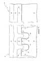
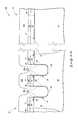
- FIG. 1is a diagrammatic sectional view of a substrate fragment in process in accordance with an embodiment of the invention.
- FIG. 2is a view of the FIG. 1 substrate at a processing step subsequent to that shown by FIG. 1 .
- FIG. 3is a view of the FIG. 2 substrate at a processing step subsequent to that shown by FIG. 2 .
- FIG. 4is a view of the FIG. 3 substrate at a processing step subsequent to that shown by FIG. 3 .
- FIG. 5is a view of the FIG. 4 substrate at a processing step subsequent to that shown by FIG. 4 .
- FIG. 6is a view of the FIG. 5 substrate at a processing step subsequent to that shown by FIG. 5 .
- FIG. 7is a view of the FIG. 6 substrate at a processing step subsequent to that shown by FIG. 6 .
- FIG. 8is a view of the FIG. 7 substrate at a processing step subsequent to that shown by FIG. 7 .
- FIG. 9is a view of the FIG. 8 substrate at a processing step subsequent to that shown by FIG. 8 .
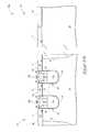
- FIG. 10is a diagrammatic sectional view of a substrate fragment in process in accordance with an embodiment of the invention.
- FIG. 11is a view of the FIG. 10 substrate at a processing step subsequent to that shown by FIG. 10 .
- FIG. 12is a view of the FIG. 11 substrate at a processing step subsequent to that shown by FIG. 11 .
- FIG. 13is a view of the FIG. 12 substrate at a processing step subsequent to that shown by FIG. 12 .
- FIG. 14is a view of the FIG. 13 substrate at a processing step subsequent to that shown by FIG. 13 .
- FIG. 15is a view of the FIG. 14 substrate at a processing step subsequent to that shown by FIG. 14 .
- FIG. 16is a view of the FIG. 15 substrate at a processing step subsequent to that shown by FIG. 15 .
- FIG. 17is a view of the FIG. 16 substrate at a processing step subsequent to that shown by FIG. 16 .
- Embodiments of the inventionencompass methods of forming a gate construction of a recessed access device.
- the discussion initiallyproceeds with reference to FIGS. 1-9 of an example method of forming recessed access device gate constructions within a memory array area and forming peripheral circuitry gate constructions in a peripheral circuitry area.
- a semiconductor substrate 10includes a memory array area 12 and a peripheral circuitry area 14 .
- semiconductor substrateor “semiconductive substrate” is defined to mean any construction comprising semiconductive material, including, but not limited to, bulk semiconductive materials such as a semiconductive wafer (either alone or in assemblies comprising other materials thereon), and semiconductive material layers (either alone or in assemblies comprising other materials).
- substraterefers to any supporting structure, including, but not limited to, the semiconductive substrates described above.
- Substrate 10may comprise semiconductive material 16 , for example monocrystalline silicon having trench isolation regions 18 formed therein.
- Active area of material 16 for device fabricationis received between or surrounded by trench isolation regions 18 .
- Example trench isolation materialis silicon dioxide which may be lined with silicon nitride.
- a sacrificial oxide 20has been formed over substrate material 16 / 18 , and photoresist-comprising material 22 has been formed thereover.
- photoresist-comprising material 22has been patterned to form elongated trench openings therein.
- Material 22has then been used as an etch mask in etching into material 20 / 16 in forming recessed access device trenches 24 within semiconductive material 16 within memory array area 12 .
- Such trenchesmay also be formed in peripheral circuitry area 14 which, however, is not germane to embodiments of the invention.
- Trench openings(not shown) may also be formed through materials 22 and 20 into trench isolation 18 . Trenches 24 would likely be elongated in a longitudinal direction into and out of the plane of the page upon which FIG. 2 lies.
- the respective recessed access device trenchesmay be considered as having opposing semiconductive material sidewalls 28 and a semiconductive material base 30 extending there-between.
- DRAMdynamic random access memory
- oxide 20(not shown) and photoresist-comprising material 22 (not shown) have been removed from the substrate.
- gate dielectric 26has been formed over semiconductive material sidewalls 28 within trenches 24 in memory array area 12 and over semiconductive material 16 within peripheral circuitry area 14 .
- Suchmay be homogenous or non-homogenous and comprise any suitable dielectric material, with thermally grown silicon dioxide being an example. Further, such may be subjected to plasma nitridation processing, or other processing, during or after its deposition. Any suitable thickness may be used, with from about 80 Angstroms to about 100 Angstroms being an example.
- First conductive gate material 32has been deposited over gate dielectric 26 within semiconductive material trenches 24 in memory array area 12 and over gate dielectric 26 in peripheral circuitry area 14 .
- Material 32may be deposited to physically contact gate dielectric 26 .
- Material 32may be homogenous or non-homogenous, and may comprise any one or combination of elemental metals, alloys of elemental metals, conductive metal compounds, and/or conductively doped semiconductive material. Conductively doped polysilicon is one example.
- An example thickness for first conductive gate material 32is about half of an ultimate desired thickness of the conductive portions of gate constructions in the peripheral circuitry area where gate constructions are to be there-fabricated.
- an example thickness rangeis from about 250 Angstroms to about 450 Angstroms, with about 350 Angstroms being a specific example.
- an etch barrier 34may be deposited over first conductive gate material 32 in memory array area 12 and in peripheral circuitry area 14 .
- An example materialis silicon nitride deposited to an example thickness of about 300 Angstroms. Such may be used to protect the outermost surface of first conductive gate material 32 within peripheral circuitry area 14 during processing specific to memory array area 12 .
- a photoresist-comprising material 36may be formed over etch barrier 34 . Such may be homogenous or non-homogenous comprising multiple different composition materials and/or layers.
- photoresist-comprising material 36has been patterned to form a mask having openings there-through, with such mask being used to etch trench openings 38 through first conductive gate material 32 over recessed access device trenches 24 within memory array area 12 .
- Trench openings 38may be of the same size and configuration of trench openings 24 which were formed within material 16 .
- Trench openings 38may be considered as having opposing sidewalls 35 of first conductive gate material 32 .
- first conductive gate material 32has been recessed within trenches 24 , for example by etching, to expose sidewalls of elevationally outermost portions of gate dielectric 26 within semiconductive material trenches 24 in memory array area 12 .
- first conductive gate material 32 within respective recessed access device trenches 24has a planar elevationally outermost (upper) surface 37 that spans completely across the respective trench 24 between gate dielectric 26 elevationally inward of an outermost surface 17 of semiconductive material 16 immediately adjacent the respective trenches 24 .
- surface 37 of the first conductive gate material within the respective trenches 24is recessed from about 200 Angstroms to about 500 Angstroms from surface 17 .
- surface 37 within the respective trenches 24is recessed from about 200 Angstroms to about one-third of the depths of trenches 24 within material 16 from surface 17 .
- photoresist-comprising material 36(not shown) has been removed. Further in one example embodiment where an etch barrier 34 (not shown) has been used, such has also been removed from the substrate after trench openings 38 have been etched. Subsequently, spacer material 40 has been deposited over first conductive gate material 32 , including within trench openings 38 over material 32 within recessed access device trenches 24 . In one embodiment, material 40 is dielectric. Material 40 may be homogenous or non-homogenous, and regardless may be of the same composition or different composition from that of gate dielectric 26 .
- anisotropically etched sidewall spacers 42have been formed from material 40 . Such may be received laterally over the opposing sidewalls of the exposed portions of gate dielectric 26 that are within semiconductive material trenches 24 . Such may also be received laterally over opposing sidewalls 35 of first conductive gate material 32 of trench openings 38 . Spacers 42 may be formed to be wider at their bottoms/bases than at their tops, for example as shown. Such describes and depicts but one method of forming a pair of sidewall spacers laterally over opposing sidewalls of a gate dielectric and elevationally over first conductive gate material. Alternate etching or growth techniques may be used.
- a pair of spacersmay be interconnected within one or both opposing ends of a trench, but regardless may be considered as a pair of spacers in at least one straight line cross section, for example as shown. Further, the spacers may or may not be dielectric. Spacers 42 may be considered as having laterally outermost sidewall surfaces 48 and laterally innermost sidewall surfaces 49 .
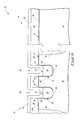
- second conductive gate material 46has been deposited within semiconductive material trenches 24 between the respective pairs of sidewall spacers 42 and may physically contact and be in electrical connection with first conductive gate material 32 in memory array area 12 .
- Second conductive gate material 46has also been formed over and may physically contact and be in electrical connection with first conductive gate material 32 in peripheral circuitry area 14 .
- Second conductive gate material 46may be homogenous or non-homogenous, may or may not be of the same composition as first gate material 32 , and may be deposited to any suitable thickness. In some embodiments, second conductive gate material 46 may not be deposited into physical contact with first conductive gate material 32 . In one embodiment, second conductive gate material 46 may be deposited above spacers 42 .
- embodiments of the inventioncontemplate second conductive material 46 not being deposited or remaining in a finished circuitry construction with spacers 42 .
- other materialmay be deposited over second conductive gate material 46 .
- an insulatorsuch as silicon nitride may be deposited over gate material 46 to be used in the fabrication of insulative gate caps.
- second conductive gate material 46 within memory array area 12has been etched or otherwise removed to form recessed access device gate constructions 50 within memory array area 12 .
- first and second conductive gate materials 32 , 46have been etched or otherwise removed within peripheral circuitry area 14 to form peripheral circuitry gate constructions 52 .
- Such masking stepmay comprise, by way of example, deposition and patterning of a photosensitive material (not shown) to comprise masking blocks (not shown) of the same lateral and longitudinal configuration of the elevationally outermost portions of gate constructions 50 and 52 .
- Some or all of gate dielectric 26may or may not (as shown) be removed laterally outward of gate constructions 50 and/or gate constructions 52 .
- the patterning of second conductive gate material 46forms the respective conductive portions of gate constructions 50 to be wider in cross section above and below dielectric spacers 42 than there-between.
- the conductive portion of a gate construction 50 in the depicted exampleis encompassed by the combination of first conductive gate material 32 and second conductive gate material 46 .
- Such conductive portionhas a greater or wider upper lateral expanse A above dielectric spacers 42 and a greater or wider lateral expanse B below dielectric spacers 42 than every portion of lateral expanse C between dielectric spacers 42 .
- the patterningmay form second conductive gate material 46 to have laterally outermost sidewall surfaces 54 that are laterally coincident with those surfaces 48 of dielectric spacers 42 . Provision of dielectric spacers 42 results in an effective widening of the gate dielectric region for the transistor at the locations where the outermost surfaces of material 16 join or define trenches 24 . Such may reduce GIDL in circuit operation.
- Processingmay proceed subsequently in fabrication of completed field effect transistor devices using recessed access gate constructions 50 within memory array area 12 and gate constructions 52 within peripheral circuitry area 14 .
- suitable source/drain regions 54have been fabricated in memory array area 12 and peripheral circuitry area 14 .
- two recessed access device transistors in memory array area 12are shown as comprising part of DRAM circuitry.
- a center and shared source/drain region 54 of the two transistorsis shown connected schematically with a data/sense line 58 (for example a bit line), while the laterally outer source/drain regions 54 are shown connected schematically with a respective capacitor 56 , thus forming two memory cells of DRAM circuitry.
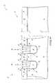
- Example alternate embodiments of a method of forming recessed access device gate constructions within a memory array area and peripheral circuitry gate constructions in a peripheral circuitry areaare next described with reference to FIGS. 10-17 .
- Like numerals from the above-described embodimentshave been used where appropriate, with some construction differences being indicated with the suffix “a” or with different numerals.
- peripheral circuitry gate dielectric 60 and conductive peripheral circuitry gate material 62have been formed over peripheral circuitry area 14 and over memory array area 12 of semiconductor substrate 10 a . Attributes of dielectric material 60 may be as described above with respect to gate dielectric 26 .
- Example conductive peripheral circuitry gate material 62may be as described above with respect to first and second conductive gate materials 32 , 46 .
- an oxidation barrier 64may be formed over conductive peripheral gate material 62 in memory array area 12 and in peripheral circuitry area 14 .
- An example materialis silicon nitride deposited to an example thickness of about 300 Angstroms.
- recessed access device trenches 24have been etched to within semiconductive material 16 by etching through material 64 , 62 and 60 . Such may be formed using photolithographic or other method.
- memory array gate dielectric 26 ahas been formed over sidewalls 28 of semiconductive material 16 within trenches 24 in memory array area 12 .
- Suchmay be formed by any suitable method and have any of the attributes of dielectric 26 described above. If formed by oxidation and where conductive peripheral circuitry gate material 62 comprises an oxidizable material, such may also form laterally over sidewalls of such material above semiconductive material trenches 24 , as shown.
- first conductive gate material 32 ahas been deposited over a memory array gate dielectric 26 a within semiconductive material trenches 24 in memory array area 12 and over peripheral circuitry area 14 . Such may have any one or more of the attributes described above with respect to first conductive gate material 32 .
- first conductive gate material 32 ahas been etched to recess it within trenches 24 to below surfaces 17 of semiconductive material 16 adjacent trenches 24 within memory array area 12 . Further, opposing sidewalls of a portion of memory array gate dielectric 26 a within trenches 24 have been exposed. Any one or more attributes as described above with respect to the processing of FIG. 4 may be used in the processing of FIG. 14 .
- spacers 42 aare also received laterally over opposing sidewalls of conductive peripheral circuitry gate material 62 above surfaces 17 of semiconductive material 16 adjacent trenches 24 .
- material 26 ais received between spacers 42 a and material 62 .
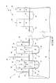
- second conductive gate material 46has been deposited within trenches 24 between the respective pairs of spacers 42 a in electrical connection with first conductive gate material 32 a within memory array area 12 . Such has also been deposited over and in electrical connection with conductive peripheral circuitry gate material 62 in peripheral circuitry area 14 . Any one or more of the attributes described above may be used or result.
- second conductive gate material 46 within memory array area 12has been etched or otherwise removed to form recessed access device gate constructions 50 a within memory array area 12 .
- second conductive gate material 46 and conductive peripheral circuitry gate material 62have been etched or otherwise removed within peripheral circuitry area 14 to form peripheral circuitry gate constructions 52 a .
- peripheral circuitry gate dielectric 60may (as shown) or may not be removed laterally outward of gate constructions 50 a and/or gate constructions 52 a . Any attribute and/or subsequent processing may occur or result as described above, or otherwise.
- a method of forming a gate construction of a recessed access deviceincludes forming a pair of sidewall spacers laterally over opposing sidewalls of a gate dielectric and above first conductive gate material.
- the gate dielectric, the first conductive gate material, and the spacers over which such are formedare collectively received within a trench formed in semiconductive material.
- Such spacersmay or may not project outwardly of the semiconductive material in which the trench is formed. Further, other material may or may not be received over the semiconductive material in which the trench is formed.
- the above-described embodimentsshow spacers 42 and 42 a as projecting elevationally outward of a trench 24 in semiconductive material 16 .
- such spacersmight have uppermost surfaces which are elevationally coincident with uppermost surfaces 17 of material 16 immediately adjacent a trench 24 , or which are recessed within a trench 24 below such surfaces 17 .
- greater reduction in GIDLmay occur by having dielectric spacers 42 / 42 a project elevationally outward of material 16 as shown.
- second conductive gate materialis deposited within the semiconductive material trench between the pair of sidewall spacers to be in electrical connection with the first conductive gate material.
- One or more attributesmay be as described above with respect to composition, deposition, and any subsequent patterning with respect to the first and second conductive gate materials.
- a method of forming a gate construction of a recessed access devicecomprises forming gate dielectric and first conductive gate material within a trench in semiconductive material.
- the first conductive gate materialis recessed, for example by etching, within the trench to have an elevationally outermost (upper) surface that spans completely across the trench between the gate dielectric.
- a pair of etched sidewall spacersis formed within the trench laterally over opposing sidewalls of the gate dielectric and over the first conductive gate material.
- Second conductive gate materialis deposited within the trench between the pair of etched sidewall spacers in electrical connection with the first conductive gate material.
- Embodiments of the inventionalso encompass recessed access device gate constructions independent of method of fabrication.
- a gate constructioncomprises a trench within semiconductive material, with the trench comprising semiconductive material sidewalls and a semiconductive material base extending between the semiconductive material sidewalls.
- a gate dielectric liningis received over the semiconductive material trench sidewalls and the semiconductive material trench base.
- a pair of laterally spaced and laterally opposed blocksis received within an upper portion of the trench, and which project laterally into the trench.
- the above-described sidewall spacersare example such blocks. Regardless, the blocks are laterally thicker than thickness of the gate dielectric lining that is received over the trench sidewalls and the trench base.
- Conductive gate materialis received within the trench between and below the blocks, and extends elevationally outward of the semiconductive material trench to elevationally over the dielectric blocks.
- the conductive portion of the gate constructionis wider in cross section above and below the blocks than there-between. Any one or other attributes of the constructions as described above and/or shown in the drawings may constitute an attribute of such a recessed access device gate construction.
Landscapes
- Engineering & Computer Science (AREA)
- Manufacturing & Machinery (AREA)
- Physics & Mathematics (AREA)
- Condensed Matter Physics & Semiconductors (AREA)
- General Physics & Mathematics (AREA)
- Computer Hardware Design (AREA)
- Microelectronics & Electronic Packaging (AREA)
- Power Engineering (AREA)
- Semiconductor Memories (AREA)
- Insulated Gate Type Field-Effect Transistor (AREA)
Abstract
Description
Claims (21)
Priority Applications (2)
| Application Number | Priority Date | Filing Date | Title |
|---|---|---|---|
| US12/833,071US8859367B2 (en) | 2010-07-09 | 2010-07-09 | Gate constructions of recessed access devices and methods of forming gate constructions of recessed access devices |
| US14/487,201US20150001605A1 (en) | 2010-07-09 | 2014-09-16 | Gate Constructions Of Recessed Access Devices And Methods Of Forming Gate Constructions Of Recessed Access Devices |
Applications Claiming Priority (1)
| Application Number | Priority Date | Filing Date | Title |
|---|---|---|---|
| US12/833,071US8859367B2 (en) | 2010-07-09 | 2010-07-09 | Gate constructions of recessed access devices and methods of forming gate constructions of recessed access devices |
Related Child Applications (1)
| Application Number | Title | Priority Date | Filing Date |
|---|---|---|---|
| US14/487,201DivisionUS20150001605A1 (en) | 2010-07-09 | 2014-09-16 | Gate Constructions Of Recessed Access Devices And Methods Of Forming Gate Constructions Of Recessed Access Devices |
Publications (2)
| Publication Number | Publication Date |
|---|---|
| US20120009772A1 US20120009772A1 (en) | 2012-01-12 |
| US8859367B2true US8859367B2 (en) | 2014-10-14 |
Family
ID=45438906
Family Applications (2)
| Application Number | Title | Priority Date | Filing Date |
|---|---|---|---|
| US12/833,071Active2032-02-10US8859367B2 (en) | 2010-07-09 | 2010-07-09 | Gate constructions of recessed access devices and methods of forming gate constructions of recessed access devices |
| US14/487,201AbandonedUS20150001605A1 (en) | 2010-07-09 | 2014-09-16 | Gate Constructions Of Recessed Access Devices And Methods Of Forming Gate Constructions Of Recessed Access Devices |
Family Applications After (1)
| Application Number | Title | Priority Date | Filing Date |
|---|---|---|---|
| US14/487,201AbandonedUS20150001605A1 (en) | 2010-07-09 | 2014-09-16 | Gate Constructions Of Recessed Access Devices And Methods Of Forming Gate Constructions Of Recessed Access Devices |
Country Status (1)
| Country | Link |
|---|---|
| US (2) | US8859367B2 (en) |
Cited By (6)
| Publication number | Priority date | Publication date | Assignee | Title |
|---|---|---|---|---|
| US20150243782A1 (en)* | 2014-02-25 | 2015-08-27 | Micron Technology, Inc. | Transistor-Containing Constructions and Memory Arrays |
| US20160141380A1 (en)* | 2014-11-14 | 2016-05-19 | Infineon Technologies Austria Ag | Method for Manufacturing a Semiconductor Device, and Semiconductor Device |
| US20220246757A1 (en)* | 2021-02-04 | 2022-08-04 | Nanya Technology Corporation | Semiconductor device and method for manufacturing the same |
| US20230083560A1 (en)* | 2021-09-14 | 2023-03-16 | Sandisk Technologies Llc | Field effect transistors with gate fins and method of making the same |
| US11967626B2 (en) | 2021-09-14 | 2024-04-23 | Sandisk Technologies Llc | Field effect transistors with gate fins and method of making the same |
| US12279445B2 (en) | 2021-09-14 | 2025-04-15 | SanDisk Technologies, Inc. | Field effect transistors with gate fins and method of making the same |
Families Citing this family (13)
| Publication number | Priority date | Publication date | Assignee | Title |
|---|---|---|---|---|
| US7282401B2 (en) | 2005-07-08 | 2007-10-16 | Micron Technology, Inc. | Method and apparatus for a self-aligned recessed access device (RAD) transistor gate |
| US7867851B2 (en) | 2005-08-30 | 2011-01-11 | Micron Technology, Inc. | Methods of forming field effect transistors on substrates |
| US7700441B2 (en)* | 2006-02-02 | 2010-04-20 | Micron Technology, Inc. | Methods of forming field effect transistors, methods of forming field effect transistor gates, methods of forming integrated circuitry comprising a transistor gate array and circuitry peripheral to the gate array, and methods of forming integrated circuitry comprising a transistor gate array including first gates and second grounded isolation gates |
| US7602001B2 (en)* | 2006-07-17 | 2009-10-13 | Micron Technology, Inc. | Capacitorless one transistor DRAM cell, integrated circuitry comprising an array of capacitorless one transistor DRAM cells, and method of forming lines of capacitorless one transistor DRAM cells |
| US7772632B2 (en)* | 2006-08-21 | 2010-08-10 | Micron Technology, Inc. | Memory arrays and methods of fabricating memory arrays |
| US7589995B2 (en)* | 2006-09-07 | 2009-09-15 | Micron Technology, Inc. | One-transistor memory cell with bias gate |
| US7923373B2 (en) | 2007-06-04 | 2011-04-12 | Micron Technology, Inc. | Pitch multiplication using self-assembling materials |
| US8530306B2 (en)* | 2011-05-27 | 2013-09-10 | Nanya Technology Corp. | Method of forming a slit recess channel gate |
| US9136177B2 (en) | 2012-07-30 | 2015-09-15 | Globalfoundries Inc. | Methods of forming transistor devices with high-k insulation layers and the resulting devices |
| US9123784B2 (en)* | 2012-08-21 | 2015-09-01 | Nanya Technology Corporation | Memory process and memory structure made thereby |
| TWI497609B (en)* | 2013-04-10 | 2015-08-21 | Inotera Memories Inc | Semiconductor memory system |
| US11189623B2 (en) | 2018-12-18 | 2021-11-30 | Micron Technology, Inc. | Apparatuses, memory devices, and electronic systems |
| US11515313B2 (en)* | 2020-06-22 | 2022-11-29 | Taiwan Semiconductor Manufacturing Company Limited | Gated ferroelectric memory cells for memory cell array and methods of forming the same |
Citations (20)
| Publication number | Priority date | Publication date | Assignee | Title |
|---|---|---|---|---|
| US6063669A (en) | 1996-02-26 | 2000-05-16 | Nec Corporation | Manufacturing method of semiconductor memory device having a trench gate electrode |
| US6168996B1 (en) | 1997-08-28 | 2001-01-02 | Hitachi, Ltd. | Method of fabricating semiconductor device |
| US6214670B1 (en) | 1999-07-22 | 2001-04-10 | Taiwan Semiconductor Manufacturing Company | Method for manufacturing short-channel, metal-gate CMOS devices with superior hot carrier performance |
| US6235639B1 (en) | 1998-11-25 | 2001-05-22 | Micron Technology, Inc. | Method of making straight wall containers and the resultant containers |
| US20040092115A1 (en) | 2002-11-07 | 2004-05-13 | Winbond Electronics Corp. | Memory device having isolation trenches with different depths and the method for making the same |
| US6744097B2 (en) | 2001-08-02 | 2004-06-01 | Samsung Electronics Co., Ltd. | EEPROM memory cell and method of forming the same |
| US20040224476A1 (en) | 2000-01-25 | 2004-11-11 | Satoru Yamada | Semiconductor integrated circuit device |
| US6825093B2 (en)* | 2001-09-28 | 2004-11-30 | Infineon Technologies Ag | Process window enhancement for deep trench spacer conservation |
| US6884679B2 (en)* | 2002-07-18 | 2005-04-26 | Hynix Semiconductor Inc. | Flash memory cell and method of manufacturing the same and programming/erasing/reading method of flash memory cell |
| US7022573B2 (en)* | 2003-01-17 | 2006-04-04 | Nanya Technology Corporation | Stack gate with tip vertical memory and method for fabricating the same |
| US20060113588A1 (en)* | 2004-11-29 | 2006-06-01 | Sillicon-Based Technology Corp. | Self-aligned trench-type DMOS transistor structure and its manufacturing methods |
| US7122429B2 (en) | 2002-10-18 | 2006-10-17 | Kabushiki Kaisha Toshiba | Semiconductor memory and method of manufacturing the same |
| US20070264771A1 (en) | 2006-05-11 | 2007-11-15 | Venkatesan Ananthan | Dual work function recessed access device and methods of forming |
| US20080128800A1 (en) | 2006-12-04 | 2008-06-05 | Samsung Electronics Co., Ltd. | Field effect transistors including recessed forked gate structures and methods of fabricating the same |
| US20080242024A1 (en) | 2007-03-27 | 2008-10-02 | Elpida Memory, Inc. | Method of manufacturing semiconductor device |
| US20090026522A1 (en) | 2007-07-09 | 2009-01-29 | Venkatesan Ananthan | Semiconductor device comprising transistor structures and methods for forming same |
| US20090173994A1 (en)* | 2008-01-07 | 2009-07-09 | Samsung Electronics Co., Ltd. | Recess gate transistor |
| US7576389B2 (en)* | 2006-06-22 | 2009-08-18 | Elpida Memory, Inc. | Semiconductor device and manufacture method thereof |
| US7589995B2 (en) | 2006-09-07 | 2009-09-15 | Micron Technology, Inc. | One-transistor memory cell with bias gate |
| US7700441B2 (en) | 2006-02-02 | 2010-04-20 | Micron Technology, Inc. | Methods of forming field effect transistors, methods of forming field effect transistor gates, methods of forming integrated circuitry comprising a transistor gate array and circuitry peripheral to the gate array, and methods of forming integrated circuitry comprising a transistor gate array including first gates and second grounded isolation gates |
Family Cites Families (1)
| Publication number | Priority date | Publication date | Assignee | Title |
|---|---|---|---|---|
| KR100714900B1 (en)* | 2006-06-09 | 2007-05-04 | 삼성전자주식회사 | Semiconductor device having a buried gate electrode and a manufacturing method thereof |
- 2010
- 2010-07-09USUS12/833,071patent/US8859367B2/enactiveActive
- 2014
- 2014-09-16USUS14/487,201patent/US20150001605A1/ennot_activeAbandoned
Patent Citations (21)
| Publication number | Priority date | Publication date | Assignee | Title |
|---|---|---|---|---|
| US6063669A (en) | 1996-02-26 | 2000-05-16 | Nec Corporation | Manufacturing method of semiconductor memory device having a trench gate electrode |
| US6168996B1 (en) | 1997-08-28 | 2001-01-02 | Hitachi, Ltd. | Method of fabricating semiconductor device |
| US6235639B1 (en) | 1998-11-25 | 2001-05-22 | Micron Technology, Inc. | Method of making straight wall containers and the resultant containers |
| US6214670B1 (en) | 1999-07-22 | 2001-04-10 | Taiwan Semiconductor Manufacturing Company | Method for manufacturing short-channel, metal-gate CMOS devices with superior hot carrier performance |
| US20040224476A1 (en) | 2000-01-25 | 2004-11-11 | Satoru Yamada | Semiconductor integrated circuit device |
| US6744097B2 (en) | 2001-08-02 | 2004-06-01 | Samsung Electronics Co., Ltd. | EEPROM memory cell and method of forming the same |
| US6825093B2 (en)* | 2001-09-28 | 2004-11-30 | Infineon Technologies Ag | Process window enhancement for deep trench spacer conservation |
| US6884679B2 (en)* | 2002-07-18 | 2005-04-26 | Hynix Semiconductor Inc. | Flash memory cell and method of manufacturing the same and programming/erasing/reading method of flash memory cell |
| US7122429B2 (en) | 2002-10-18 | 2006-10-17 | Kabushiki Kaisha Toshiba | Semiconductor memory and method of manufacturing the same |
| US20040092115A1 (en) | 2002-11-07 | 2004-05-13 | Winbond Electronics Corp. | Memory device having isolation trenches with different depths and the method for making the same |
| US7022573B2 (en)* | 2003-01-17 | 2006-04-04 | Nanya Technology Corporation | Stack gate with tip vertical memory and method for fabricating the same |
| US20060113588A1 (en)* | 2004-11-29 | 2006-06-01 | Sillicon-Based Technology Corp. | Self-aligned trench-type DMOS transistor structure and its manufacturing methods |
| US7700441B2 (en) | 2006-02-02 | 2010-04-20 | Micron Technology, Inc. | Methods of forming field effect transistors, methods of forming field effect transistor gates, methods of forming integrated circuitry comprising a transistor gate array and circuitry peripheral to the gate array, and methods of forming integrated circuitry comprising a transistor gate array including first gates and second grounded isolation gates |
| US7902028B2 (en) | 2006-02-02 | 2011-03-08 | Micron Technology, Inc. | Methods of forming field effect transistors, methods of forming field effect transistor gates, methods of forming integrated circuitry comprising a transistor gate array and circuitry peripheral to the gate array, and methods of forming integrated circuitry comprising a transistor gate array including first gates and second grounded isolation gates |
| US20070264771A1 (en) | 2006-05-11 | 2007-11-15 | Venkatesan Ananthan | Dual work function recessed access device and methods of forming |
| US7576389B2 (en)* | 2006-06-22 | 2009-08-18 | Elpida Memory, Inc. | Semiconductor device and manufacture method thereof |
| US7589995B2 (en) | 2006-09-07 | 2009-09-15 | Micron Technology, Inc. | One-transistor memory cell with bias gate |
| US20080128800A1 (en) | 2006-12-04 | 2008-06-05 | Samsung Electronics Co., Ltd. | Field effect transistors including recessed forked gate structures and methods of fabricating the same |
| US20080242024A1 (en) | 2007-03-27 | 2008-10-02 | Elpida Memory, Inc. | Method of manufacturing semiconductor device |
| US20090026522A1 (en) | 2007-07-09 | 2009-01-29 | Venkatesan Ananthan | Semiconductor device comprising transistor structures and methods for forming same |
| US20090173994A1 (en)* | 2008-01-07 | 2009-07-09 | Samsung Electronics Co., Ltd. | Recess gate transistor |
Non-Patent Citations (1)
| Title |
|---|
| Tran et al., "A 58nm Trench DRAM Technology", IEEE Xplore, Apr. 19, 2010, 4 pgs. |
Cited By (12)
| Publication number | Priority date | Publication date | Assignee | Title |
|---|---|---|---|---|
| US20150243782A1 (en)* | 2014-02-25 | 2015-08-27 | Micron Technology, Inc. | Transistor-Containing Constructions and Memory Arrays |
| US9240477B2 (en)* | 2014-02-25 | 2016-01-19 | Micron Technology, Inc. | Transistor-containing constructions and memory arrays |
| US20160141380A1 (en)* | 2014-11-14 | 2016-05-19 | Infineon Technologies Austria Ag | Method for Manufacturing a Semiconductor Device, and Semiconductor Device |
| US9728617B2 (en)* | 2014-11-14 | 2017-08-08 | Infineon Technologies Austria Ag | Method for manufacturing a semiconductor device |
| US10304935B2 (en) | 2014-11-14 | 2019-05-28 | Infineon Technologies Austria Ag | Semiconductor device having a trench gate electrode |
| US20220246757A1 (en)* | 2021-02-04 | 2022-08-04 | Nanya Technology Corporation | Semiconductor device and method for manufacturing the same |
| US11424360B1 (en)* | 2021-02-04 | 2022-08-23 | Nanya Technology Corporation | Semiconductor device and method for manufacturing the same |
| US11721759B2 (en) | 2021-02-04 | 2023-08-08 | Nanya Technology Corporation | Method for forming gate metal structure having portions with different heights |
| US20230083560A1 (en)* | 2021-09-14 | 2023-03-16 | Sandisk Technologies Llc | Field effect transistors with gate fins and method of making the same |
| US11967626B2 (en) | 2021-09-14 | 2024-04-23 | Sandisk Technologies Llc | Field effect transistors with gate fins and method of making the same |
| US12015084B2 (en)* | 2021-09-14 | 2024-06-18 | Sandisk Technologies Llc | Field effect transistors with gate fins and method of making the same |
| US12279445B2 (en) | 2021-09-14 | 2025-04-15 | SanDisk Technologies, Inc. | Field effect transistors with gate fins and method of making the same |
Also Published As
| Publication number | Publication date |
|---|---|
| US20150001605A1 (en) | 2015-01-01 |
| US20120009772A1 (en) | 2012-01-12 |
Similar Documents
| Publication | Publication Date | Title |
|---|---|---|
| US8859367B2 (en) | Gate constructions of recessed access devices and methods of forming gate constructions of recessed access devices | |
| TWI385734B (en) | A method of forming a field effect transistor, forming a field effect transistor gate, forming a method having an integrated circuit of a transistor gate array and a circuit around the gate array, and forming a first gate Method for integrating circuit of transistor gate array of second grounded insulated gate | |
| US9613967B1 (en) | Memory device and method of fabricating the same | |
| US8518788B2 (en) | Methods of forming a plurality of capacitors | |
| US20120292716A1 (en) | Dram structure with buried word lines and fabrication thereof, and ic structure and fabrication thereof | |
| US10163908B2 (en) | Array of conductive lines individually extending transversally across and elevationally over a mid-portion of individual active area regions | |
| US20130049072A1 (en) | Arrays Of Recessed Access Devices, Methods Of Forming Recessed Access Gate Constructions, And Methods Of Forming Isolation Gate Constructions In The Fabrication Of Recessed Access Devices | |
| JP2006279009A (en) | Method of manufacturing semiconductor element | |
| TWI701763B (en) | Transistor structure and semiconductor layout structure | |
| US8039327B2 (en) | Transistor forming methods | |
| US20110263089A1 (en) | Method for fabricating semiconductor device | |
| US8748978B2 (en) | Sense-amp transistor of semiconductor device and method for manufacturing the same | |
| US7816208B2 (en) | Method of manufacturing semiconductor device having trench-gate transistor | |
| KR100876883B1 (en) | Semiconductor device, manufacturing method thereof and gate forming method of semiconductor device | |
| US7692251B2 (en) | Transistor for semiconductor device and method of forming the same | |
| US20130146966A1 (en) | Semiconductor structure with enhanced cap and fabrication method thereof | |
| CN102142394A (en) | Semiconductor device and method for manufacturing the same | |
| JP2016046414A (en) | Method of manufacturing semiconductor device | |
| US20140110773A1 (en) | Semiconductor device including line-type active region and method for manufacturing the same | |
| US7700435B2 (en) | Method for fabricating deep trench DRAM array | |
| JP3685997B2 (en) | Substrate having recess suitable for integrated circuit device and method for manufacturing the same | |
| US20090061592A1 (en) | Semiconductor device and manufacturing method thereof | |
| KR101052871B1 (en) | Semiconductor device and manufacturing method thereof | |
| KR100688543B1 (en) | Recess gate type semiconductor device and manufacturing method thereof | |
| KR100636669B1 (en) | Manufacturing Method of DRAM Memory Cell |
Legal Events
| Date | Code | Title | Description |
|---|---|---|---|
| AS | Assignment | Owner name:MICRON TECHNOLOGY, INC., IDAHO Free format text:ASSIGNMENT OF ASSIGNORS INTEREST;ASSIGNORS:MATHEW, SURAJ;GUHA, JAYDIP;REEL/FRAME:024657/0341 Effective date:20100706 | |
| FEPP | Fee payment procedure | Free format text:PAYOR NUMBER ASSIGNED (ORIGINAL EVENT CODE: ASPN); ENTITY STATUS OF PATENT OWNER: LARGE ENTITY | |
| STCF | Information on status: patent grant | Free format text:PATENTED CASE | |
| AS | Assignment | Owner name:U.S. BANK NATIONAL ASSOCIATION, AS COLLATERAL AGENT, CALIFORNIA Free format text:SECURITY INTEREST;ASSIGNOR:MICRON TECHNOLOGY, INC.;REEL/FRAME:038669/0001 Effective date:20160426 Owner name:U.S. BANK NATIONAL ASSOCIATION, AS COLLATERAL AGEN Free format text:SECURITY INTEREST;ASSIGNOR:MICRON TECHNOLOGY, INC.;REEL/FRAME:038669/0001 Effective date:20160426 | |
| AS | Assignment | Owner name:MORGAN STANLEY SENIOR FUNDING, INC., AS COLLATERAL AGENT, MARYLAND Free format text:PATENT SECURITY AGREEMENT;ASSIGNOR:MICRON TECHNOLOGY, INC.;REEL/FRAME:038954/0001 Effective date:20160426 Owner name:MORGAN STANLEY SENIOR FUNDING, INC., AS COLLATERAL Free format text:PATENT SECURITY AGREEMENT;ASSIGNOR:MICRON TECHNOLOGY, INC.;REEL/FRAME:038954/0001 Effective date:20160426 | |
| AS | Assignment | Owner name:U.S. BANK NATIONAL ASSOCIATION, AS COLLATERAL AGENT, CALIFORNIA Free format text:CORRECTIVE ASSIGNMENT TO CORRECT THE REPLACE ERRONEOUSLY FILED PATENT #7358718 WITH THE CORRECT PATENT #7358178 PREVIOUSLY RECORDED ON REEL 038669 FRAME 0001. ASSIGNOR(S) HEREBY CONFIRMS THE SECURITY INTEREST;ASSIGNOR:MICRON TECHNOLOGY, INC.;REEL/FRAME:043079/0001 Effective date:20160426 Owner name:U.S. BANK NATIONAL ASSOCIATION, AS COLLATERAL AGEN Free format text:CORRECTIVE ASSIGNMENT TO CORRECT THE REPLACE ERRONEOUSLY FILED PATENT #7358718 WITH THE CORRECT PATENT #7358178 PREVIOUSLY RECORDED ON REEL 038669 FRAME 0001. ASSIGNOR(S) HEREBY CONFIRMS THE SECURITY INTEREST;ASSIGNOR:MICRON TECHNOLOGY, INC.;REEL/FRAME:043079/0001 Effective date:20160426 | |
| MAFP | Maintenance fee payment | Free format text:PAYMENT OF MAINTENANCE FEE, 4TH YEAR, LARGE ENTITY (ORIGINAL EVENT CODE: M1551) Year of fee payment:4 | |
| AS | Assignment | Owner name:JPMORGAN CHASE BANK, N.A., AS COLLATERAL AGENT, ILLINOIS Free format text:SECURITY INTEREST;ASSIGNORS:MICRON TECHNOLOGY, INC.;MICRON SEMICONDUCTOR PRODUCTS, INC.;REEL/FRAME:047540/0001 Effective date:20180703 Owner name:JPMORGAN CHASE BANK, N.A., AS COLLATERAL AGENT, IL Free format text:SECURITY INTEREST;ASSIGNORS:MICRON TECHNOLOGY, INC.;MICRON SEMICONDUCTOR PRODUCTS, INC.;REEL/FRAME:047540/0001 Effective date:20180703 | |
| AS | Assignment | Owner name:MICRON TECHNOLOGY, INC., IDAHO Free format text:RELEASE BY SECURED PARTY;ASSIGNOR:U.S. BANK NATIONAL ASSOCIATION, AS COLLATERAL AGENT;REEL/FRAME:047243/0001 Effective date:20180629 | |
| AS | Assignment | Owner name:MICRON TECHNOLOGY, INC., IDAHO Free format text:RELEASE BY SECURED PARTY;ASSIGNOR:MORGAN STANLEY SENIOR FUNDING, INC., AS COLLATERAL AGENT;REEL/FRAME:050937/0001 Effective date:20190731 | |
| AS | Assignment | Owner name:MICRON TECHNOLOGY, INC., IDAHO Free format text:RELEASE BY SECURED PARTY;ASSIGNOR:JPMORGAN CHASE BANK, N.A., AS COLLATERAL AGENT;REEL/FRAME:051028/0001 Effective date:20190731 Owner name:MICRON SEMICONDUCTOR PRODUCTS, INC., IDAHO Free format text:RELEASE BY SECURED PARTY;ASSIGNOR:JPMORGAN CHASE BANK, N.A., AS COLLATERAL AGENT;REEL/FRAME:051028/0001 Effective date:20190731 | |
| MAFP | Maintenance fee payment | Free format text:PAYMENT OF MAINTENANCE FEE, 8TH YEAR, LARGE ENTITY (ORIGINAL EVENT CODE: M1552); ENTITY STATUS OF PATENT OWNER: LARGE ENTITY Year of fee payment:8 |