US8854863B2 - Arrays of nonvolatile memory cells and methods of forming arrays of nonvolatile memory cells - Google Patents
Arrays of nonvolatile memory cells and methods of forming arrays of nonvolatile memory cellsDownload PDFInfo
- Publication number
- US8854863B2 US8854863B2US13/970,369US201313970369AUS8854863B2US 8854863 B2US8854863 B2US 8854863B2US 201313970369 AUS201313970369 AUS 201313970369AUS 8854863 B2US8854863 B2US 8854863B2
- Authority
- US
- United States
- Prior art keywords
- tiers
- electrode lines
- lines
- memory cells
- array
- Prior art date
- Legal status (The legal status is an assumption and is not a legal conclusion. Google has not performed a legal analysis and makes no representation as to the accuracy of the status listed.)
- Active
Links
- 238000000034methodMethods0.000titleclaimsabstractdescription25
- 238000003491arrayMethods0.000titledescription10
- 239000000463materialSubstances0.000claimsabstractdescription183
- 239000004020conductorSubstances0.000claimsabstractdescription44
- 239000000203mixtureSubstances0.000claimsdescription13
- 238000005530etchingMethods0.000claimsdescription6
- 210000004027cellAnatomy0.000description58
- 239000003989dielectric materialSubstances0.000description26
- 239000000758substrateSubstances0.000description22
- 239000002019doping agentSubstances0.000description14
- VYPSYNLAJGMNEJ-UHFFFAOYSA-NSilicium dioxideChemical compoundO=[Si]=OVYPSYNLAJGMNEJ-UHFFFAOYSA-N0.000description13
- 230000000873masking effectEffects0.000description13
- 238000010276constructionMethods0.000description12
- 229910052751metalInorganic materials0.000description11
- 239000002184metalSubstances0.000description11
- 150000002500ionsChemical class0.000description10
- GWEVSGVZZGPLCZ-UHFFFAOYSA-NTitan oxideChemical compoundO=[Ti]=OGWEVSGVZZGPLCZ-UHFFFAOYSA-N0.000description8
- IJGRMHOSHXDMSA-UHFFFAOYSA-NAtomic nitrogenChemical compoundN#NIJGRMHOSHXDMSA-UHFFFAOYSA-N0.000description6
- 239000000377silicon dioxideSubstances0.000description6
- 235000012239silicon dioxideNutrition0.000description6
- XUIMIQQOPSSXEZ-UHFFFAOYSA-NSiliconChemical compound[Si]XUIMIQQOPSSXEZ-UHFFFAOYSA-N0.000description5
- QVGXLLKOCUKJST-UHFFFAOYSA-Natomic oxygenChemical compound[O]QVGXLLKOCUKJST-UHFFFAOYSA-N0.000description5
- 229910052731fluorineInorganic materials0.000description5
- 229910044991metal oxideInorganic materials0.000description5
- 150000004706metal oxidesChemical class0.000description5
- 229910052760oxygenInorganic materials0.000description5
- 239000001301oxygenSubstances0.000description5
- 229910052710siliconInorganic materials0.000description5
- 239000010703siliconSubstances0.000description5
- YCKRFDGAMUMZLT-UHFFFAOYSA-NFluorine atomChemical compound[F]YCKRFDGAMUMZLT-UHFFFAOYSA-N0.000description4
- KDLHZDBZIXYQEI-UHFFFAOYSA-NPalladiumChemical compound[Pd]KDLHZDBZIXYQEI-UHFFFAOYSA-N0.000description4
- 229910052581Si3N4Inorganic materials0.000description4
- NINIDFKCEFEMDL-UHFFFAOYSA-NSulfurChemical compound[S]NINIDFKCEFEMDL-UHFFFAOYSA-N0.000description4
- 239000002800charge carrierSubstances0.000description4
- 229910052802copperInorganic materials0.000description4
- 239000010949copperSubstances0.000description4
- 238000000151depositionMethods0.000description4
- 239000011737fluorineSubstances0.000description4
- 239000012634fragmentSubstances0.000description4
- 229910052757nitrogenInorganic materials0.000description4
- 238000000059patterningMethods0.000description4
- BASFCYQUMIYNBI-UHFFFAOYSA-NplatinumChemical compound[Pt]BASFCYQUMIYNBI-UHFFFAOYSA-N0.000description4
- 239000004065semiconductorSubstances0.000description4
- HQVNEWCFYHHQES-UHFFFAOYSA-Nsilicon nitrideChemical compoundN12[Si]34N5[Si]62N3[Si]51N64HQVNEWCFYHHQES-UHFFFAOYSA-N0.000description4
- 229910002704AlGaNInorganic materials0.000description3
- 229910052787antimonyInorganic materials0.000description3
- WATWJIUSRGPENY-UHFFFAOYSA-Nantimony atomChemical compound[Sb]WATWJIUSRGPENY-UHFFFAOYSA-N0.000description3
- 125000004429atomChemical group0.000description3
- 229910017052cobaltInorganic materials0.000description3
- 239000010941cobaltSubstances0.000description3
- GUTLYIVDDKVIGB-UHFFFAOYSA-Ncobalt atomChemical compound[Co]GUTLYIVDDKVIGB-UHFFFAOYSA-N0.000description3
- 230000008021depositionEffects0.000description3
- 238000004519manufacturing processMethods0.000description3
- 239000002243precursorSubstances0.000description3
- 229910052709silverInorganic materials0.000description3
- 239000004215Carbon black (E152)Substances0.000description2
- RYGMFSIKBFXOCR-UHFFFAOYSA-NCopperChemical compound[Cu]RYGMFSIKBFXOCR-UHFFFAOYSA-N0.000description2
- UQSXHKLRYXJYBZ-UHFFFAOYSA-NIron oxideChemical compound[Fe]=OUQSXHKLRYXJYBZ-UHFFFAOYSA-N0.000description2
- ATUOYWHBWRKTHZ-UHFFFAOYSA-NPropaneChemical compoundCCCATUOYWHBWRKTHZ-UHFFFAOYSA-N0.000description2
- -1WOxInorganic materials0.000description2
- 238000000429assemblyMethods0.000description2
- 230000000712assemblyEffects0.000description2
- 230000015572biosynthetic processEffects0.000description2
- 239000002131composite materialSubstances0.000description2
- 239000007772electrode materialSubstances0.000description2
- 238000004070electrodepositionMethods0.000description2
- 150000002222fluorine compoundsChemical class0.000description2
- 239000007789gasSubstances0.000description2
- 229910052732germaniumInorganic materials0.000description2
- GNPVGFCGXDBREM-UHFFFAOYSA-Ngermanium atomChemical compound[Ge]GNPVGFCGXDBREM-UHFFFAOYSA-N0.000description2
- 229930195733hydrocarbonNatural products0.000description2
- 150000002430hydrocarbonsChemical class0.000description2
- 229910001635magnesium fluorideInorganic materials0.000description2
- 238000001465metallisationMethods0.000description2
- 150000002739metalsChemical class0.000description2
- 150000004767nitridesChemical class0.000description2
- QJGQUHMNIGDVPM-UHFFFAOYSA-Nnitrogen groupChemical group[N]QJGQUHMNIGDVPM-UHFFFAOYSA-N0.000description2
- 229910052763palladiumInorganic materials0.000description2
- 229910052697platinumInorganic materials0.000description2
- 238000001289rapid thermal chemical vapour depositionMethods0.000description2
- 229910052714telluriumInorganic materials0.000description2
- PORWMNRCUJJQNO-UHFFFAOYSA-Ntellurium atomChemical compound[Te]PORWMNRCUJJQNO-UHFFFAOYSA-N0.000description2
- 239000011800void materialSubstances0.000description2
- HZNVUJQVZSTENZ-UHFFFAOYSA-N2,3-dichloro-5,6-dicyano-1,4-benzoquinoneChemical compoundClC1=C(Cl)C(=O)C(C#N)=C(C#N)C1=OHZNVUJQVZSTENZ-UHFFFAOYSA-N0.000description1
- OBXNVGDOZGTMKV-UHFFFAOYSA-N2-tert-butyltellanyl-2-methylpropaneChemical compoundCC(C)(C)[Te]C(C)(C)COBXNVGDOZGTMKV-UHFFFAOYSA-N0.000description1
- SNLFYGIUTYKKOE-UHFFFAOYSA-N4-n,4-n-bis(4-aminophenyl)benzene-1,4-diamineChemical compoundC1=CC(N)=CC=C1N(C=1C=CC(N)=CC=1)C1=CC=C(N)C=C1SNLFYGIUTYKKOE-UHFFFAOYSA-N0.000description1
- 229910002969CaMnO3Inorganic materials0.000description1
- 229910018999CoSi2Inorganic materials0.000description1
- QPLDLSVMHZLSFG-UHFFFAOYSA-NCopper oxideChemical compound[Cu]=OQPLDLSVMHZLSFG-UHFFFAOYSA-N0.000description1
- 239000005751Copper oxideSubstances0.000description1
- 229910016553CuOxInorganic materials0.000description1
- 229910002531CuTeInorganic materials0.000description1
- 229910005842GeS2Inorganic materials0.000description1
- 229910000618GeSbTeInorganic materials0.000description1
- 229910005867GeSe2Inorganic materials0.000description1
- 229910000673Indium arsenideInorganic materials0.000description1
- VEQPNABPJHWNSG-UHFFFAOYSA-NNickel(2+)Chemical compound[Ni+2]VEQPNABPJHWNSG-UHFFFAOYSA-N0.000description1
- BUGBHKTXTAQXES-UHFFFAOYSA-NSeleniumChemical compound[Se]BUGBHKTXTAQXES-UHFFFAOYSA-N0.000description1
- BQCADISMDOOEFD-UHFFFAOYSA-NSilverChemical compound[Ag]BQCADISMDOOEFD-UHFFFAOYSA-N0.000description1
- 229910002370SrTiO3Inorganic materials0.000description1
- 229910004166TaNInorganic materials0.000description1
- 229910003071TaONInorganic materials0.000description1
- 229910003081TiO2−xInorganic materials0.000description1
- 229910010252TiO3Inorganic materials0.000description1
- 229910010282TiONInorganic materials0.000description1
- ATJFFYVFTNAWJD-UHFFFAOYSA-NTinChemical compound[Sn]ATJFFYVFTNAWJD-UHFFFAOYSA-N0.000description1
- 239000007983Tris bufferSubstances0.000description1
- 229910003134ZrOxInorganic materials0.000description1
- 239000011149active materialSubstances0.000description1
- 239000000654additiveSubstances0.000description1
- 230000000996additive effectEffects0.000description1
- 229910045601alloyInorganic materials0.000description1
- 239000000956alloySubstances0.000description1
- XAGFODPZIPBFFR-UHFFFAOYSA-NaluminiumChemical group[Al]XAGFODPZIPBFFR-UHFFFAOYSA-N0.000description1
- PNEYBMLMFCGWSK-UHFFFAOYSA-Naluminium oxideInorganic materials[O-2].[O-2].[O-2].[Al+3].[Al+3]PNEYBMLMFCGWSK-UHFFFAOYSA-N0.000description1
- 229910021417amorphous siliconInorganic materials0.000description1
- 229910002113barium titanateInorganic materials0.000description1
- 230000006399behaviorEffects0.000description1
- 229910002056binary alloyInorganic materials0.000description1
- 210000003850cellular structureAnatomy0.000description1
- 150000004770chalcogenidesChemical class0.000description1
- 238000012512characterization methodMethods0.000description1
- 238000006243chemical reactionMethods0.000description1
- 238000005229chemical vapour depositionMethods0.000description1
- 229910000431copper oxideInorganic materials0.000description1
- 229910052593corundumInorganic materials0.000description1
- 238000009826distributionMethods0.000description1
- 238000001312dry etchingMethods0.000description1
- 239000003792electrolyteSubstances0.000description1
- GNBHRKFJIUUOQI-UHFFFAOYSA-NfluoresceinChemical compoundO1C(=O)C2=CC=CC=C2C21C1=CC=C(O)C=C1OC1=CC(O)=CC=C21GNBHRKFJIUUOQI-UHFFFAOYSA-N0.000description1
- 125000001153fluoro groupChemical groupF*0.000description1
- 239000003574free electronSubstances0.000description1
- 229910001938gadolinium oxideInorganic materials0.000description1
- 229940075613gadolinium oxideDrugs0.000description1
- CMIHHWBVHJVIGI-UHFFFAOYSA-Ngadolinium(iii) oxideChemical compound[O-2].[O-2].[O-2].[Gd+3].[Gd+3]CMIHHWBVHJVIGI-UHFFFAOYSA-N0.000description1
- 229910000449hafnium oxideInorganic materials0.000description1
- WIHZLLGSGQNAGK-UHFFFAOYSA-Nhafnium(4+);oxygen(2-)Chemical compound[O-2].[O-2].[Hf+4]WIHZLLGSGQNAGK-UHFFFAOYSA-N0.000description1
- CJNBYAVZURUTKZ-UHFFFAOYSA-Nhafnium(IV) oxideInorganic materialsO=[Hf]=OCJNBYAVZURUTKZ-UHFFFAOYSA-N0.000description1
- RPQDHPTXJYYUPQ-UHFFFAOYSA-Nindium arsenideChemical compound[In]#[As]RPQDHPTXJYYUPQ-UHFFFAOYSA-N0.000description1
- 239000012212insulatorSubstances0.000description1
- 230000037427ion transportEffects0.000description1
- 230000004807localizationEffects0.000description1
- CPLXHLVBOLITMK-UHFFFAOYSA-Nmagnesium oxideInorganic materials[Mg]=OCPLXHLVBOLITMK-UHFFFAOYSA-N0.000description1
- 150000002736metal compoundsChemical class0.000description1
- 229910021421monocrystalline siliconInorganic materials0.000description1
- JKUUTODNPMRHHZ-UHFFFAOYSA-Nn-methyl-n-[tris(dimethylamino)germyl]methanamineChemical compoundCN(C)[Ge](N(C)C)(N(C)C)N(C)CJKUUTODNPMRHHZ-UHFFFAOYSA-N0.000description1
- 229910001453nickel ionInorganic materials0.000description1
- 229910000484niobium oxideInorganic materials0.000description1
- URLJKFSTXLNXLG-UHFFFAOYSA-Nniobium(5+);oxygen(2-)Chemical compound[O-2].[O-2].[O-2].[O-2].[O-2].[Nb+5].[Nb+5]URLJKFSTXLNXLG-UHFFFAOYSA-N0.000description1
- 125000004433nitrogen atomChemical groupN*0.000description1
- QGLKJKCYBOYXKC-UHFFFAOYSA-NnonaoxidotritungstenChemical compoundO=[W]1(=O)O[W](=O)(=O)O[W](=O)(=O)O1QGLKJKCYBOYXKC-UHFFFAOYSA-N0.000description1
- 125000004430oxygen atomChemical groupO*0.000description1
- RVTZCBVAJQQJTK-UHFFFAOYSA-Noxygen(2-);zirconium(4+)Chemical compound[O-2].[O-2].[Zr+4]RVTZCBVAJQQJTK-UHFFFAOYSA-N0.000description1
- 230000002093peripheral effectEffects0.000description1
- 229920000642polymerPolymers0.000description1
- 239000002861polymer materialSubstances0.000description1
- 239000001294propaneSubstances0.000description1
- 238000000197pyrolysisMethods0.000description1
- 229910052711seleniumInorganic materials0.000description1
- 239000011669seleniumSubstances0.000description1
- 229910021332silicideInorganic materials0.000description1
- 229910052814silicon oxideInorganic materials0.000description1
- 239000002210silicon-based materialSubstances0.000description1
- 239000004332silverSubstances0.000description1
- 239000007787solidSubstances0.000description1
- 230000003068static effectEffects0.000description1
- 229910052712strontiumInorganic materials0.000description1
- 229910014031strontium zirconium oxideInorganic materials0.000description1
- 229910052717sulfurInorganic materials0.000description1
- 239000011593sulfurSubstances0.000description1
- 239000003115supporting electrolyteSubstances0.000description1
- PBCFLUZVCVVTBY-UHFFFAOYSA-Ntantalum pentoxideInorganic materialsO=[Ta](=O)O[Ta](=O)=OPBCFLUZVCVVTBY-UHFFFAOYSA-N0.000description1
- 229910052718tinInorganic materials0.000description1
- 229910052721tungstenInorganic materials0.000description1
- 229910001930tungsten oxideInorganic materials0.000description1
- 229910001845yogo sapphireInorganic materials0.000description1
- 229910001928zirconium oxideInorganic materials0.000description1
Images


Classifications
- H—ELECTRICITY
- H10—SEMICONDUCTOR DEVICES; ELECTRIC SOLID-STATE DEVICES NOT OTHERWISE PROVIDED FOR
- H10B—ELECTRONIC MEMORY DEVICES
- H10B63/00—Resistance change memory devices, e.g. resistive RAM [ReRAM] devices
- H10B63/20—Resistance change memory devices, e.g. resistive RAM [ReRAM] devices comprising selection components having two electrodes, e.g. diodes
- H—ELECTRICITY
- H10—SEMICONDUCTOR DEVICES; ELECTRIC SOLID-STATE DEVICES NOT OTHERWISE PROVIDED FOR
- H10N—ELECTRIC SOLID-STATE DEVICES NOT OTHERWISE PROVIDED FOR
- H10N70/00—Solid-state devices having no potential barriers, and specially adapted for rectifying, amplifying, oscillating or switching
- H10N70/011—Manufacture or treatment of multistable switching devices
- H10N70/021—Formation of switching materials, e.g. deposition of layers
- G—PHYSICS
- G11—INFORMATION STORAGE
- G11C—STATIC STORES
- G11C5/00—Details of stores covered by group G11C11/00
- G11C5/02—Disposition of storage elements, e.g. in the form of a matrix array
- G—PHYSICS
- G11—INFORMATION STORAGE
- G11C—STATIC STORES
- G11C5/00—Details of stores covered by group G11C11/00
- G11C5/06—Arrangements for interconnecting storage elements electrically, e.g. by wiring
- H—ELECTRICITY
- H01—ELECTRIC ELEMENTS
- H01L—SEMICONDUCTOR DEVICES NOT COVERED BY CLASS H10
- H01L21/00—Processes or apparatus adapted for the manufacture or treatment of semiconductor or solid state devices or of parts thereof
- H01L21/02—Manufacture or treatment of semiconductor devices or of parts thereof
- H01L21/04—Manufacture or treatment of semiconductor devices or of parts thereof the devices having potential barriers, e.g. a PN junction, depletion layer or carrier concentration layer
- H01L21/18—Manufacture or treatment of semiconductor devices or of parts thereof the devices having potential barriers, e.g. a PN junction, depletion layer or carrier concentration layer the devices having semiconductor bodies comprising elements of Group IV of the Periodic Table or AIIIBV compounds with or without impurities, e.g. doping materials
- H01L21/30—Treatment of semiconductor bodies using processes or apparatus not provided for in groups H01L21/20 - H01L21/26
- H01L21/302—Treatment of semiconductor bodies using processes or apparatus not provided for in groups H01L21/20 - H01L21/26 to change their surface-physical characteristics or shape, e.g. etching, polishing, cutting
- H01L27/1021—
- H01L27/2409—
- H01L27/2463—
- H01L27/2472—
- H01L27/2481—
- H01L45/04—
- H01L45/08—
- H01L45/085—
- H01L45/1233—
- H01L45/14—
- H01L45/142—
- H01L45/143—
- H01L45/144—
- H01L45/145—
- H01L45/146—
- H01L45/147—
- H01L45/16—
- H01L45/1616—
- H01L45/165—
- H—ELECTRICITY
- H10—SEMICONDUCTOR DEVICES; ELECTRIC SOLID-STATE DEVICES NOT OTHERWISE PROVIDED FOR
- H10B—ELECTRONIC MEMORY DEVICES
- H10B63/00—Resistance change memory devices, e.g. resistive RAM [ReRAM] devices
- H10B63/80—Arrangements comprising multiple bistable or multi-stable switching components of the same type on a plane parallel to the substrate, e.g. cross-point arrays
- H10B63/82—Arrangements comprising multiple bistable or multi-stable switching components of the same type on a plane parallel to the substrate, e.g. cross-point arrays the switching components having a common active material layer
- H—ELECTRICITY
- H10—SEMICONDUCTOR DEVICES; ELECTRIC SOLID-STATE DEVICES NOT OTHERWISE PROVIDED FOR
- H10B—ELECTRONIC MEMORY DEVICES
- H10B63/00—Resistance change memory devices, e.g. resistive RAM [ReRAM] devices
- H10B63/80—Arrangements comprising multiple bistable or multi-stable switching components of the same type on a plane parallel to the substrate, e.g. cross-point arrays
- H10B63/84—Arrangements comprising multiple bistable or multi-stable switching components of the same type on a plane parallel to the substrate, e.g. cross-point arrays arranged in a direction perpendicular to the substrate, e.g. 3D cell arrays
- H—ELECTRICITY
- H10—SEMICONDUCTOR DEVICES; ELECTRIC SOLID-STATE DEVICES NOT OTHERWISE PROVIDED FOR
- H10N—ELECTRIC SOLID-STATE DEVICES NOT OTHERWISE PROVIDED FOR
- H10N70/00—Solid-state devices having no potential barriers, and specially adapted for rectifying, amplifying, oscillating or switching
- H10N70/011—Manufacture or treatment of multistable switching devices
- H10N70/021—Formation of switching materials, e.g. deposition of layers
- H10N70/023—Formation of switching materials, e.g. deposition of layers by chemical vapor deposition, e.g. MOCVD, ALD
- H—ELECTRICITY
- H10—SEMICONDUCTOR DEVICES; ELECTRIC SOLID-STATE DEVICES NOT OTHERWISE PROVIDED FOR
- H10N—ELECTRIC SOLID-STATE DEVICES NOT OTHERWISE PROVIDED FOR
- H10N70/00—Solid-state devices having no potential barriers, and specially adapted for rectifying, amplifying, oscillating or switching
- H10N70/011—Manufacture or treatment of multistable switching devices
- H10N70/041—Modification of switching materials after formation, e.g. doping
- H10N70/043—Modification of switching materials after formation, e.g. doping by implantation
- H—ELECTRICITY
- H10—SEMICONDUCTOR DEVICES; ELECTRIC SOLID-STATE DEVICES NOT OTHERWISE PROVIDED FOR
- H10N—ELECTRIC SOLID-STATE DEVICES NOT OTHERWISE PROVIDED FOR
- H10N70/00—Solid-state devices having no potential barriers, and specially adapted for rectifying, amplifying, oscillating or switching
- H10N70/20—Multistable switching devices, e.g. memristors
- H10N70/24—Multistable switching devices, e.g. memristors based on migration or redistribution of ionic species, e.g. anions, vacancies
- H10N70/245—Multistable switching devices, e.g. memristors based on migration or redistribution of ionic species, e.g. anions, vacancies the species being metal cations, e.g. programmable metallization cells
- H—ELECTRICITY
- H10—SEMICONDUCTOR DEVICES; ELECTRIC SOLID-STATE DEVICES NOT OTHERWISE PROVIDED FOR
- H10N—ELECTRIC SOLID-STATE DEVICES NOT OTHERWISE PROVIDED FOR
- H10N70/00—Solid-state devices having no potential barriers, and specially adapted for rectifying, amplifying, oscillating or switching
- H10N70/801—Constructional details of multistable switching devices
- H10N70/821—Device geometry
- H10N70/826—Device geometry adapted for essentially vertical current flow, e.g. sandwich or pillar type devices
- H—ELECTRICITY
- H10—SEMICONDUCTOR DEVICES; ELECTRIC SOLID-STATE DEVICES NOT OTHERWISE PROVIDED FOR
- H10N—ELECTRIC SOLID-STATE DEVICES NOT OTHERWISE PROVIDED FOR
- H10N70/00—Solid-state devices having no potential barriers, and specially adapted for rectifying, amplifying, oscillating or switching
- H10N70/801—Constructional details of multistable switching devices
- H10N70/881—Switching materials
- H10N70/882—Compounds of sulfur, selenium or tellurium, e.g. chalcogenides
- H10N70/8822—Sulfides, e.g. CuS
- H—ELECTRICITY
- H10—SEMICONDUCTOR DEVICES; ELECTRIC SOLID-STATE DEVICES NOT OTHERWISE PROVIDED FOR
- H10N—ELECTRIC SOLID-STATE DEVICES NOT OTHERWISE PROVIDED FOR
- H10N70/00—Solid-state devices having no potential barriers, and specially adapted for rectifying, amplifying, oscillating or switching
- H10N70/801—Constructional details of multistable switching devices
- H10N70/881—Switching materials
- H10N70/882—Compounds of sulfur, selenium or tellurium, e.g. chalcogenides
- H10N70/8825—Selenides, e.g. GeSe
- H—ELECTRICITY
- H10—SEMICONDUCTOR DEVICES; ELECTRIC SOLID-STATE DEVICES NOT OTHERWISE PROVIDED FOR
- H10N—ELECTRIC SOLID-STATE DEVICES NOT OTHERWISE PROVIDED FOR
- H10N70/00—Solid-state devices having no potential barriers, and specially adapted for rectifying, amplifying, oscillating or switching
- H10N70/801—Constructional details of multistable switching devices
- H10N70/881—Switching materials
- H10N70/882—Compounds of sulfur, selenium or tellurium, e.g. chalcogenides
- H10N70/8828—Tellurides, e.g. GeSbTe
- H—ELECTRICITY
- H10—SEMICONDUCTOR DEVICES; ELECTRIC SOLID-STATE DEVICES NOT OTHERWISE PROVIDED FOR
- H10N—ELECTRIC SOLID-STATE DEVICES NOT OTHERWISE PROVIDED FOR
- H10N70/00—Solid-state devices having no potential barriers, and specially adapted for rectifying, amplifying, oscillating or switching
- H10N70/801—Constructional details of multistable switching devices
- H10N70/881—Switching materials
- H10N70/883—Oxides or nitrides
- H10N70/8833—Binary metal oxides, e.g. TaOx
- H—ELECTRICITY
- H10—SEMICONDUCTOR DEVICES; ELECTRIC SOLID-STATE DEVICES NOT OTHERWISE PROVIDED FOR
- H10N—ELECTRIC SOLID-STATE DEVICES NOT OTHERWISE PROVIDED FOR
- H10N70/00—Solid-state devices having no potential barriers, and specially adapted for rectifying, amplifying, oscillating or switching
- H10N70/801—Constructional details of multistable switching devices
- H10N70/881—Switching materials
- H10N70/883—Oxides or nitrides
- H10N70/8836—Complex metal oxides, e.g. perovskites, spinels
- G—PHYSICS
- G11—INFORMATION STORAGE
- G11C—STATIC STORES
- G11C13/00—Digital stores characterised by the use of storage elements not covered by groups G11C11/00, G11C23/00, or G11C25/00
- G11C13/0002—Digital stores characterised by the use of storage elements not covered by groups G11C11/00, G11C23/00, or G11C25/00 using resistive RAM [RRAM] elements
- G11C13/0004—Digital stores characterised by the use of storage elements not covered by groups G11C11/00, G11C23/00, or G11C25/00 using resistive RAM [RRAM] elements comprising amorphous/crystalline phase transition cells
- G—PHYSICS
- G11—INFORMATION STORAGE
- G11C—STATIC STORES
- G11C2213/00—Indexing scheme relating to G11C13/00 for features not covered by this group
- G11C2213/70—Resistive array aspects
- G11C2213/71—Three dimensional array
Definitions
- Embodiments disclosed hereinpertain to nonvolatile memory cells, to arrays of nonvolatile memory cells, and to methods of forming arrays of nonvolatile memory cells
- Memoryis one type of integrated circuitry, and is used in computer systems for storing data. Such is usually fabricated in one or more arrays of individual memory cells.
- the memory cellsmight be volatile, semi-volatile, or nonvolatile.
- Nonvolatile memory cellscan store data for extended periods of time, in many instances including when the computer is turned off. Volatile memory dissipates and therefore requires being refreshed/rewritten, in many instances multiple times per second.
- the smallest unit in each arrayis termed as a memory cell and is configured to retain or store memory in at least two different selectable states. In a binary system, the states are considered as either a “0” or a “1”. In other systems, at least some individual memory cells may be configured to store more than two levels or states of information.
- the smallest and simplest memory cellwill be comprised of two current conductive electrodes having a programmable material there-between.
- the programmable materialis selected or designed to be configured in a selected one of at least two different resistive states to enable storing of information by an individual memory cell.
- the reading of the cellcomprises determination of which of the states the programmable material is in, and the writing of information to the cell comprises placing the programmable material in a predetermined resistive state.
- Some programmable materialsmay contain mobile charge carriers larger than electrons and holes, for example ions in some example applications. Regardless, the programmable materials may be converted from one memory state to another by moving the mobile charge carriers therein to alter a distribution of charge density within the programmable materials.
- Some example memory devices that utilize ions as mobile charge carriersare resistive RAM (RRAM) cells, which can include classes of memory cells containing multivalent oxides, and which can include memristors in some specific applications.
- RRAMresistive RAM
- Other example memory devices that utilize ions as charge carriersare programmable metallization cells (PMCs); which may be alternatively referred to as a conductive bridging RAM (CBRAM), nanobridge memory, or electrolyte memory.
- CBRAMconductive bridging RAM
- the RRAM cellsmay contain programmable material sandwiched between a pair of electrodes.
- the programming of the RRAM cellsmay comprise transitioning the programmable material between a first memory state in which charge density is relatively uniformly dispersed throughout the material and a second memory state in which the charge density is concentrated in a specific region of the material (for instance, a region closer to one electrode than the other).
- a PMCmay similarly have programmable material sandwiched between a pair of current conductive electrodes.
- the PMC programmable materialcomprises ion conductive material, for example a suitable chalcogenide or any of various suitable oxides.
- a suitable voltage applied across the electrodesgenerates current conductive super-ionic clusters or filaments. Such result from ion transport through the ion conductive material which grows the clusters/filaments from one of the electrodes (the cathode), through the ion conductive material, and toward the other electrode (the anode).
- the clusters or filamentscreate current conductive paths between the electrodes.
- An opposite voltage applied across the electrodesessentially reverses the process and thus removes the current conductive paths.
- a PMCthus comprises a high resistance state (corresponding to the state lacking a current conductive filament or clusters between the electrodes) and a low resistance state (corresponding to the state having a current conductive filament or clusters between the electrodes), with such states being reversibly interchangeable with one another.
- FIG. 1is a diagrammatic, exploded, isometric view of a portion of an array of nonvolatile memory cells in accordance with an embodiment of the invention.
- FIG. 2is an enlarged view of a portion of FIG. 1 .
- FIG. 3is a sectional view of FIG. 2 taken through line 3 - 3 in FIG. 2 .
- FIG. 4is a diagrammatic, exploded, isometric view of a portion of an array of nonvolatile memory cells in accordance with an embodiment of the invention.
- FIG. 5is a circuit schematic of a portion of a FIG. 4-like array.
- FIGS. 6-19are diagrammatic top views and sectional views of a substrate fragment in process in ultimately producing an array of nonvolatile memory cells in accordance with an embodiment of the invention.
- FIGS. 20-43are diagrammatic top and sectional views of a substrate fragment in process in ultimately producing an array of nonvolatile memory cells in accordance with an embodiment of the invention.
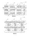
- Embodiments of the inventioninclude arrays of nonvolatile memory cells, methods of forming a horizontal array of nonvolatile memory cells, and methods of forming an array of vertically stacked tiers of nonvolatile memory cells. Some example embodiments are initially described with reference to FIGS. 1-3 of an array 10 of vertically stacked tiers of memory cells.
- FIG. 1shows a portion of an array area within which a plurality of nonvolatile memory cells 16 has been fabricated.
- Logic circuitry(not shown) may be fabricated outside of the array area. Control and/or other peripheral circuitry (not shown) for operating the memory array may or may not fully or partially within the array area, with an example array area as a minimum encompassing all of the memory cells of a given array/sub-array.
- multiple sub-arraysmight also be fabricated and operated independently, in tandem, or otherwise relative one another. As used in this document, a “sub-array” may also be considered as an array.
- FIG. 1depicts two vertically stacked tiers 12 , 14 of individual memory cells 16 .
- One or more tiersmay be elevationally outward of tier 12 and/or elevationally inward of tier 14 .
- array 10would be fabricated relative to a suitable base substrate (not shown) which may be homogenous or non-homogenous, for example comprising multiple different composition materials and/or layers.
- a suitable base substrate(not shown) which may be homogenous or non-homogenous, for example comprising multiple different composition materials and/or layers.
- suchmay comprise bulk monocrystalline silicon and/or a semiconductor-on-insulator substrate.
- suchmay comprise dielectric material having conductive contacts or vias formed therein which extend vertically or otherwise into current conductive electrical connection with electronic device components, regions, or material elevationally inward of the dielectric material.
- verticalis a direction generally orthogonal to a primary surface relative to which the substrate is processed during fabrication and which may be considered to define a generally horizontal direction.
- vertical and horizontalas used herein are generally perpendicular directions relative one another independent of orientation of the substrate in three-dimensional space.
- elevational and “elevationally”are with reference to the vertical direction from a base substrate upon which the circuitry is fabricated.
- the base substratemay or may not be a semiconductor substrate.
- semiconductor substrateor “semiconductive substrate” is defined to mean any construction comprising semiconductive material, including, but not limited to, bulk semiconductive materials such as a semiconductive wafer (either alone or in assemblies comprising other materials thereon), and semiconductive material layers (either alone or in assemblies comprising other materials).
- substraterefers to any supporting structure, including, but not limited to, the semiconductive substrates described above.
- FIG. 1is exploded in the vertical direction for clarity. Tiers 12 and 14 may be much more vertically closer one another than depicted, and separated by a suitable dielectric (not shown). Further, array 10 would likely be encompassed within/encapsulated by dielectric which is not shown in any of the figures for clarity of operative memory cell components within the array.
- Vertical tiers 12 , 14may be of the same or different respective construction(s). In one embodiment, all of such are of the same construction, for example perhaps to achieve an ultimate highest density and/or for ease in fabrication. Regardless, at least some of the individual vertical tiers may be characterized by certain attributes example embodiments of which are described with reference to FIGS. 1-3 with respect to an example individual memory cell 16 .
- Array 10comprises a first plurality of horizontally oriented first electrode lines 18 and a second plurality of horizontally oriented second electrode lines 20 within respective of individual tiers 12 and 14 . Second electrode lines 20 cross relative to first electrode lines 18 , and in the example embodiment are elevationally outward of first electrode lines 18 . Alternately, such may be elevationally inward of first electrode lines 18 .
- Electrode lines 18 and 20comprise current conductive material, and may be homogenous or non-homogenous.
- current conductive materialis a composition where electric current flow would inherently occur therein predominantly by movement of subatomic positive and/or negative charges when such are generated as opposed to predominantly by movement of ions.
- Example current conductive materialsare elemental metals, alloys of elemental metals, current conductive metal compounds, and conductively doped semiconductive material, including any combinations thereof.
- Individual memory cells 16comprise a crossing one of a horizontal first electrode line 18 and a horizontal second electrode line 20 .
- Suchalso comprise programmable material 22 and a select device 24 .
- Material 22 and device 24are both between electrodes 18 and 20 in electrical series connection with electrode lines 18 and 20 .
- Memory cells 16also include current conductive material 26 .
- Material 26is both between material 22 and select device 24 , and in electrical series connection with material 22 and select device 24 .
- Current conductive material 26may form part of the select device. Regardless, the depicted positions of programmable material 22 and select device 24 may be reversed. Any select device may be used, with transistors and diodes being but two examples.
- each of components 22 and 24may be homogenous or non-homogenous, and may be of the same or different shape(s), thickness(es), other dimensions, etc. relative one another.
- Current conductive material 26also may be homogenous or non-homogenous.
- Example materialsinclude any of those described above with respect to first electrode lines 18 and second electrode lines 20 . Any two or three of conductive material of components 18 , 20 and 26 may be of the same composition or of different compositions.
- the programmable materialmay be solid, gel, amorphous, crystalline, or any other suitable phase. Any programmable material may be used, with some examples being provided below.
- the programmable materialmay be isolated relative to each memory cell as shown, or alternately might be continuous along some plurality of memory cells.
- a programmable material 22 or 24may extend continuously (not shown) along first electrode line 18 or second electrode line 20 , respectively.
- FIGS. 1-3depict an example embodiment wherein immediately adjacent of components 20 , 24 , 26 , 22 and 18 are directly against one another.
- a material or structureis “directly against” another when there is at least some physical touching contact of the stated materials or structures relative one another.
- “over”encompasses “directly against” as well as construction where intervening material(s) or structure(s) result(s) in no physical touching contact of the stated materials or structures relative one another.
- Other structures than those depicted in FIGS. 1-3are contemplated with respect to whether materials or structures are directly against one another.
- material in a memory cellmay be provided between any pair of components 20 and 24 , components 24 and 26 , components 26 and 22 , and components 22 and 18 .
- the componentsare constructed and arranged such that predominant current flow into or out of the crossing one of first electrode line 18 out of or into component 22 (one of programmable material or a select device) is in a horizontal direction 28 ( FIGS. 2 and 3 ). In one embodiment, the components are constructed and arranged such that predominant current flow into or out of the crossing one of second electrode line 20 out of or into component 24 (one of programmable material or a select device) is in a vertical direction 30 ( FIG. 3 ). In one embodiment, the select device is oriented for predominant current flow relative to the respective second electrode line in the vertical direction and the programmable material is oriented for predominant current flow relative to the first electrode line in the horizontal direction.
- the programmable materialis oriented for predominant current flow relative to the second electrode line in the vertical direction and the select device is oriented for predominant current flow relative to the first electrode line in the horizontal direction.
- the crossing first electrode linemay be considered as extending along a first axis 31 ( FIG. 2 ), with horizontal direction 28 being perpendicular to first axis 31 .
- lines 18 and 20 in the depicted embodimentare shown as being straight linear. Alternately as an example, such may be curvilinear.
- FIG. 3depicts an example embodiment wherein electrode lines 20 and 18 have respective first and second planar surfaces 32 and 34 directly against which component/material 24 and 22 , respectively, is received. Further in such example, such planar surfaces constitute all surface area against which material/components 24 and 22 are against their respective crossing electrode line. Alternately as an example, interface between the electrode lines and material/components 24 and/or 22 may be with respect to entirely non-planar surfaces, a combination of planar and non-planar surfaces, or a combination of multiple stepped planar surfaces.
- FIG. 4An alternate embodiment array 10 a of vertically stacked tiers of nonvolatile memory cells is shown in FIG. 4 .
- Array 10 acomprises a plurality of vertically stacked tiers comprising multiple pairs 40 of two immediately adjacent tiers 12 a , 14 a .
- the two immediately adjacent tiers 12 a , 14 a of the respective pairs 40share one of the first or second pluralities of horizontally oriented electrode lines.
- FIG. 4depicts an example embodiment wherein second electrode lines 20 are shared. Alternately, the shared plurality of lines may be the first electrode lines (not shown). Regardless, FIG. 4 depicts two pairs 40 of immediately adjacent tiers 12 a , 14 a . Additional pairs, and/or other circuitry, may be elevationally inward and/or elevationally outward of the depicted two pairs 40 .
- One of the two immediately adjacent tiers of the respective pairsis an elevationally outer tier (i.e., tier 12 a ) and another of the two immediately adjacent tiers of the respective pairs is an elevationally inner tier (i.e., tier 14 a ).
- predominant current flow within outer tier 12 a into or out of component 22 (either programmable material or a select device) out of or into, respectively, individual of shared electrode lines 20is in the horizontal direction.
- predominant current flow within inner tier 14 a into or out of component 24 (the other of programmable material or a select device) out of or into, respectively, a shared electrode line 20is in the vertical direction. Alternate orientations may be used.
- FIG. 4depicts an embodiment wherein multiple pairs of two immediately adjacent tiers share one of the first plurality of horizontally oriented first electrode lines or the second plurality of horizontally oriented second electrode lines.
- FIG. 1depicts an alternate embodiment wherein no immediately adjacent tiers share any electrode lines of the first and second plurality of horizontally oriented electrode lines.
- An embodiment of the inventionencompasses an array of vertically stacked tiers of nonvolatile memory cells comprising multiple tiers of two immediately adjacent tiers.
- the two immediately adjacent tiers of the respective pairscomprise a shared plurality of horizontally oriented electrode lines.
- An elevationally outer of two immediately adjacent tiers of the respective pairscomprises an elevationally outer plurality of horizontally oriented electrode lines.
- An elevationally inner of the two immediately adjacent tiers of the respective pairscomprises an elevationally inner plurality of horizontally oriented electrode lines.
- Individual of the memory cellscomprise programmable material and a select device operatively between a crossing one of the shared horizontally oriented electrode lines and one of the outer or inner horizontally oriented electrode lines.
- FIG. 4depicts, by way of example, such an embodiment.
- FIG. 4depicts two pairs of immediately adjacent tiers, more than two pairs tiers may be included in the array of vertically stacked tiers.
- FIG. 5depicts an example circuit schematic representative of a FIG. 4 —like construction wherein three pairs of two immediately adjacent tiers are shown.
- individual memory cells 16as comprising a crossing one of shared electrode lines 20 and one of crossing electrode lines 18 or 18 a .
- Such further, by way of example only,are depicted as comprising programmable material 22 and a select device 24 in the form of a diode.
- the following example biasing schememay be employed for selecting the depicted memory cell 16 Z and no other of the depicted or non-depicted memory cells 16 .
- Remaining lines 18 ( i )may be biased at ground (0V). All other lines 20 ( j ) may also be biased at ground, and all other lines 18 biased at V. All unselected diodes 24 of the other memory cells 16 are thereby “off” the result of such biasing. All other lines (not shown) elevationally outward of lines 18 a may be biased at ground, while all other lines (not shown) below lines 18 may be biased at V.
- FIGS. 6-19An example of fabricating array 10 of FIG. 3 is next described with reference to FIGS. 6-19 .
- An embodiment of the inventionincludes a method of forming a horizontal array of nonvolatile memory cells, for example any one or combination of the horizontal arrays of individual of tiers 12 and 14 of FIG. 3 .
- a substrate fragment in processis indicated generally with reference numeral 50 , for example in fabricating an individual tier 14 of the FIG. 1 or other array.
- Like numerals from FIGS. 1-3have been used where appropriate, with some construction differences being indicated with the suffix “b” or with different numerals.
- Substrate 50comprises a suitable base substrate 41 ( FIG. 7 ) over which a plurality of first horizontally oriented electrode lines 18 has been formed.
- Dielectric material 42is between electrode lines 18 .
- Suchmay be homogenous or non-homogenous, with silicon nitride, doped silicon dioxide, and/or undoped silicon dioxide being examples.
- a plurality of horizontally elongated trenches 44have been formed within dielectric material 42 along only one lateral side of the respective first electrode lines 18 .
- An example technique for forming trenches 44includes subtractive patterning and etch of dielectric material 42 , for example selectively relative to the material of electrode lines 18 whereby trenches 44 self-align with respect to the depicted example one right lateral side of each electrode line 18 .
- trenches 44have been lined with one of select device material 22 or programmable material 22 that is in current conductive connection with the one lateral side of first electrode lines 18 along which trenches 44 were formed.
- FIGS. 10 and 11depict but one example resulting construction, and which may be formed by depositing the depicted material 22 followed by planarizing and/or anisotropic etching thereof to remove such from being over the depicted horizontal surfaces.
- current conductive material 26has been formed within trenches 44 laterally adjacent to and in current conductive connection with the one of select device material 22 or programmable material 22 .
- An example techniqueincludes deposition of material 26 followed by planarizing such back to the elevationally outermost surfaces of electrode lines 18 , material 22 , and dielectric material 42 .
- select device material 24 or programmable material 24is formed elevationally outward of and in current conductive connection with current conductive material 26 .
- material 24has been formed into a plurality of lines 46 that are respectively elevationally over and along current conductive material 26 within respective trenches 44 .
- suchmay be formed by deposition of material(s) 24 followed by subtractive patterning thereof.
- a plurality of second horizontally oriented electrode linesis formed over and in current conductive connection with the other of the select device material or the programmable material.
- such second electrode linesare formed to cross the first electrode lines, and in one embodiment to do so orthogonally.
- additional dielectric material 43has been deposited and planarized back at least to the elevationally outermost surface of material 24 .
- Dielectric material 43may be of the same or different composition as that of dielectric material 42 .
- second electrode material 20is deposited thereover in current conductive connection with material 24 .
- Suitable masking material 47has been formed over second electrode material 20 , and has been patterned to form second electrode line patterns 48 . In one embodiment, such comprises an example masking step.
- FIGS. 18 and 19the mask pattern of FIGS. 16 and 17 has been used as a mask while etching into material 20 to form second electrode lines 20 therefrom, and masking material 17 (not shown) has been removed.
- materials 24 , 22 , 26 , 42 , and 43have been anisotropically subtractively etched selectively relative to material 18 , for example using the FIGS. 16 and 17 masking step. Some isotropic lateral etching of any such materials selectively relative to one or more of the others may also be conducted.
- formation of the current conductive materialmay comprise subtractive patterning thereof, and in one embodiment orthogonally relative to the trenches (for example, as shown). Such may use the same masking step as other patterning, for example that of FIGS. 16 and 17 used to form lines 20 in FIGS. 18 and 19 , and regardless of whether some or all of masking material 47 remains over material 20 while etching some or all of materials 24 , 22 , 26 , 42 , and 43 . Alternately as an example, a separate dedicated masking step may be used.
- FIGS. 20-43Another example method embodiment of forming an array of vertically stacked tiers of nonvolatile memory cells largely of the example FIG. 1 embodiment is described with reference to FIGS. 20-43 .
- Like numerals from the above-described embodimentsare used where appropriate, with some construction differences being indicated with the suffix “c” or with different numerals.
- numerals 20 , 24 , 26 , 22 and 18are used to designate the materials from which such components are fabricated prior to necessarily being of the final example shapes for clarity in the drawings and ease of understanding in the description.
- substrate fragment 50 acomprises current conductive material 20 , programmable or select device material 24 , current conductive material 26 , intervening dielectric material 54 , and base substrate 41 . Accordingly, in one embodiment, such are provided relative to individual tiers 12 and 14 in which respective first and second pluralities of horizontal lines and associated individual memory cells will be formed.
- Dielectric material 54may comprise any suitable dielectric, and may be homogenous or non-homogenous. Such is also shown as being over tier 12 .
- a suitable mask patternhas been formed thereover of one or more masking materials 47 , thereby forming mask lines 48 which may be used to ultimately form lines of material 20 to produce that depicted by the example embodiment in FIG. 1 .
- suitable anisotropic dry etchinghas been conducted through each of the depicted layers 54 , 20 , 24 , 26 , 54 , 20 , 24 and 26 to base substrate 41 .
- Suchprovides but one example of forming horizontally oriented and laterally overlapping first, second, and third lines (i.e., of materials 20 , 24 and 26 , respectively) within individual tiers 12 or 14 of a plurality of vertically stacked tiers.
- First line 20 and third line 26are current conductive and of different composition.
- Second line 24is between first line 20 and second line 26 , and is of material different in composition from that of first line 20 and third line 26 .
- dielectric material 58ideally of composition different from that of dielectric material 54 .
- dielectric material 54is silicon dioxide based
- an example suitable dielectric material 58is silicon nitride. Regardless, dielectric material 58 may be homogenous or non-homogenous.
- masking material 60has been deposited and patterned as shown, for example to form masking lines respectively extending along a y-axis direction.
- dielectric material 58has been anisotropically etched through tiers 12 and 14 inwardly to base substrate 41 using material 60 as a mask. Such may be conducted selectively relative to materials 60 , 54 , 20 , and 24 whereby the cross section depicted by FIG. 26 remains largely unchanged at the end of the processing depicted by FIGS. 27 and 28 .
- masking material 60(not shown) has been removed and the void spaces of FIGS. 27 and 28 filled with dielectric material which, in one embodiment, may be of the same composition as that of material 54 and is so shown and designated in the figures.
- dielectric material 58(not shown) has been etched selectively relative to dielectric material 54 inwardly to base substrate 41 . Such thereby forms pairs of vertically extending and longitudinally aligned openings 62 a , 62 b through tiers 12 , 14 on laterally opposing sides of first lines 20 , second lines 24 , and third lines 26 that are within individual tiers 12 , 14 . Subsequently, etching has been conducted laterally through second and third lines 24 and 26 between the respective pairs of openings 62 a , 62 b to form longitudinally spaced masses 64 which extend vertically relative to first lines 20 . Masses 64 respectively comprise material of the former second lines 24 and third lines 26 .
- openings 62 a , 62 b of FIGS. 28 and 29 and remaining void spacehave been filled with dielectric material which, in one embodiment, may be of the same composition as that of material 54 and is so shown in the figures.
- masking material 66has been formed and patterned over the substrate as shown.
- exposed dielectric material 54has been anisotropically etched to form a plurality of horizontally elongated trenches 68 (along the y-axis in the FIG. 38 top view) within dielectric material 54 through tiers 12 and 14 , and which cross first lines 20 .
- trenches 68cross first lines 20 orthogonally. Additionally, trenches 68 expose only one of two opposing sides of the respective masses 64 , for example the left illustrated sides and remain covering laterally over the right illustrated sides.
- one of select device material 22 or programmable material 22is selectively grown from current conductive material 26 of the respective one exposed lateral side of masses 64 .
- example programmable materialsinclude TiON, CuO x , WO x , and TaON. Such may be grown selectively from TiN, Cu, W, or TaN, respectively, in a plasma assisted oxygen-containing ambient at from about 100° C. to about 300° C. at any suitable atmospheric, sub-atmospheric or greater than atmospheric pressure, at a suitable power of from 10 Watts to 5,000 Watts. Such may not appreciable grow from silicon nitride, silicon dioxide, platinum, and palladium.
- any such programmable material 22may so selectively grow when material 20 comprises platinum and/or palladium, and materials 24 and 54 comprise one or both of silicon dioxide or silicon nitride.
- a programmable material of germanium antimony telluriummay be selectively grown relative to a tungsten-comprising conductor 26 by CVD and/or ALD using tetrakis(dimethylamino)germane, tris(dimethylaminmo) antimony, and di-tert-butyltelluride as respective germanium, antimony, and tellurium precursors at a temperature range of from about 200° C. to about 400° C., and at a pressure range of from about 1 Torr to about 50 Torr.
- An example select device material 22comprises semiconductive material (e.g., silicon and/or InAs), for example configured to form a p/n diode.
- semiconductive material 26comprises conductively doped silicon
- a silicon-comprising select device 22may be epitaxially selectively grown from material 26 without appreciable growth on materials 41 , 54 and 51 where such do not comprise exposed elemental-form silicon.
- Suchmay be suitably conductively doped with one or both of p-type or n-type dopants during growth or may be doped subsequently (e.g., by gas phase doping and/or ion implanting).
- SiC as part of a select devicemay be selectively grown from silicon using a reaction of a hydrocarbon precursor or rapid thermal chemical vapor deposition using the pyrolysis of propane or other hydrocarbon gas precursors, for example as disclosed in P. H. Yih, et al., “SiC/Si Heterojunction Diodes Fabricated by Self-Selective and by Blanket Rapid Thermal Chemical Vapor Deposition”, IEEE Transactions on Electron Devices, Vol. 41, No. 3, (March 1994).
- AlGaNmay be selectively grown from GaN to form a p-n diode as a select device, for example as disclosed in H.
- current conductive material 18has been selectively grown from material 22 to form a plurality of horizontally oriented electrode lines 18 within individual tiers 12 and 14 .
- the so-grown horizontally oriented electrode lines 18bridge horizontally between material 22 of adjacent masses 64 .
- the growth of conductive material 18may be uniform in all directions. Yet if the distance between adjacent masses of materials 22 in a tier is sufficiently small, material 18 will merge to form a line horizontally.
- a CoSi 2 material 18may be formed by cobalt reacting with a silicon-comprising material 22 . Unreacted cobalt may then be removed by a wet etch process. Other metal silicides may be used.
- metalmay be photoselectively deposited on silicon p/n diodes, or by selective metal electrodeposition that relies on the doping of the semiconductor. Further, selective growth of conductive material 18 on material 22 may be photostimulated selective electroless Ag or Cu deposition on TiO 2 .
- An embodiment of the inventionencompasses a method of forming an array of vertically stacked tiers of nonvolatile memory cells.
- horizontally oriented current conductive lineshaving longitudinally spaced masses extending vertically therefrom are formed within individual of the tiers.
- the massesrespectively comprise current conductive material and other material between the current conductive material and the current conductive lines.
- the other materialis of different composition from that of the current conductive material and the current conductive lines.
- FIGS. 20-33show formation of example such current conductive lines 20 having longitudinally spaced masses 64 extending vertically there-from ( FIG. 33 ).
- a plurality of horizontally elongated trenchesis formed within dielectric material through the plurality of tiers and which cross the current conductive lines. Such trenches expose only one of two opposing lateral sides of the respective masses.
- the processing shown in FIGS. 33-39depicts such example processing.
- One of select device material or programmable materialis selectively grown from the current conductive material of the one lateral side of the masses.
- FIGS. 40 and 41depict such example processing.
- Example suitable such materialscomprise chalcogenide-type (for instance, materials comprising one or more of germanium, selenium, antimony, tellurium, sulfur, copper, etc.; with example chalcogenide-type materials being Ge 2 Sb 2 Te 5 , GeS 2 , GeSe 2 , CuS 2 , and CuTe) and/or oxides such as zirconium oxide, hafnium oxide, tungsten oxide, copper oxide, niobium oxide, iron oxide, silicon oxide (specifically, silicon dioxide), gadolinium oxide, etc. capable of inherently (or with additive) supporting electrolyte behavior.
- chalcogenide-typefor instance, materials comprising one or more of germanium, selenium, antimony, tellurium, sulfur, copper, etc.; with example chalcogenide-type materials being Ge 2 Sb 2 Te 5 , GeS 2 , GeSe 2 , CuS 2 , and CuTe
- oxidessuch as zirconium oxide, hafnium oxide,
- Suchmay have silver, copper, cobalt, and/or nickel ions, and/or other suitable ions, diffused therein for ionic conduction, analogously to structures disclosed in U.S. Pat. No. 7,405,967 and U.S. Patent Publication Number 2010/0193758.
- Additional example programmable materialsinclude multi-resistive state metal oxide-comprising material. Such may comprise, for example, at least two different layers or regions generally regarded as or understood to be active or passive regions, although not necessarily. Alternately, such may only comprise active material.
- Example active cell region compositions which comprise metal oxide and can be configured in multi-resistive statesinclude one or a combination of Sr x Ru y O z , Ru x O y , and In x Sn y O z .
- Example passive cell region compositionsinclude one or a combination of Al 2 O 3 , TiO 2 , and HfO 2 .
- a programmable material compositemight comprise additional metal oxide or other materials not comprising metal oxide.
- Example materials and constructions for a multi-resistive state region comprising one or more layers including a programmable metal oxide-comprising materialare described and disclosed in U.S. Pat.
- multi-resistive state metal oxide-comprising materialsencompass filament-type metal oxides, ferroelectric metal oxides and others, and whether existing or yet-to-be developed, as long as resistance of the metal oxide-comprising material can be selectively changed.
- the programmable materialmay comprise memristive material.
- such materialmay be statically programmable semiconductive material which comprises mobile dopants that are received within a dielectric such that the material is statically programmable between at least two different resistance states. At least one of the states includes localization or gathering of the mobile dopants such that a dielectric region is formed and thereby provides a higher resistance state. Further, more than two programmable resistance states may be used.
- a “mobile dopant”is a component (other than a free electron) of the semiconductive material that is movable to different locations within said dielectric during normal device operation of repeatedly programming the device between at least two different static states by application of voltage differential to the pair of electrodes.
- Examplesinclude atom vacancies in an otherwise stoichiometric material, and atom interstitials.
- mobile dopantsinclude oxygen atom vacancies in amorphous or crystalline oxides or other oxygen-containing material, nitrogen atom vacancies in amorphous or crystalline nitrides or other nitrogen-containing material, fluorine atom vacancies in amorphous or crystalline fluorides or other fluorine-containing material, and interstitial metal atoms in amorphous or crystalline oxides. More than one type of mobile dopant may be used.
- Example dielectrics in which the mobile dopants are receivedinclude suitable oxides, nitrides, and/or fluorides that are capable of localized electrical conductivity based upon sufficiently high quantity and concentration of the mobile dopants.
- the dielectric within which the mobile dopants are receivedmay or may not be homogenous independent of consideration of the mobile dopants.
- Specific example dielectricsinclude TiO 2 , AlN, and/or MgF 2 .
- Example programmable materials that comprise oxygen vacancies as mobile dopantsmay comprise a combination of TiO 2 and TiO 2-x in at least one programmed resistance state depending on location of the oxygen vacancies and the quantity of the oxygen vacancies in the locations where such are received.
- An example programmable material that comprises nitrogen vacancies as mobile dopantsis a combination of AlN and AlN 1-x in at least one programmed state depending on location of the nitrogen vacancies and the quantity of the nitrogen vacancies in the locations where such are received.
- An example programmable material that comprises fluorine vacancies as mobile dopantsmay is a combination of MgF 2 and MgF 2-x in at least one programmed resistance state depending on location of the fluorine vacancies and the quantity of the fluorine vacancies in the locations where such are received.
- the mobile dopantsmay comprise aluminum atom interstitials in a nitrogen-containing material.
- Still other example programmable materialsinclude polymer materials such as Bengala Rose, AlQ 3 Ag, Cu-TCNQ, DDQ, TAPA, and fluorescine-based polymers.
Landscapes
- Engineering & Computer Science (AREA)
- Manufacturing & Machinery (AREA)
- Physics & Mathematics (AREA)
- Condensed Matter Physics & Semiconductors (AREA)
- General Physics & Mathematics (AREA)
- Computer Hardware Design (AREA)
- Microelectronics & Electronic Packaging (AREA)
- Power Engineering (AREA)
- Chemical & Material Sciences (AREA)
- Materials Engineering (AREA)
- Semiconductor Memories (AREA)
Abstract
Description
Claims (19)
Priority Applications (2)
| Application Number | Priority Date | Filing Date | Title |
|---|---|---|---|
| US13/970,369US8854863B2 (en) | 2011-04-15 | 2013-08-19 | Arrays of nonvolatile memory cells and methods of forming arrays of nonvolatile memory cells |
| US14/276,198US9184385B2 (en) | 2011-04-15 | 2014-05-13 | Arrays of nonvolatile memory cells and methods of forming arrays of nonvolatile memory cells |
Applications Claiming Priority (2)
| Application Number | Priority Date | Filing Date | Title |
|---|---|---|---|
| US13/088,238US8537592B2 (en) | 2011-04-15 | 2011-04-15 | Arrays of nonvolatile memory cells and methods of forming arrays of nonvolatile memory cells |
| US13/970,369US8854863B2 (en) | 2011-04-15 | 2013-08-19 | Arrays of nonvolatile memory cells and methods of forming arrays of nonvolatile memory cells |
Related Parent Applications (1)
| Application Number | Title | Priority Date | Filing Date |
|---|---|---|---|
| US13/088,238ContinuationUS8537592B2 (en) | 2011-04-15 | 2011-04-15 | Arrays of nonvolatile memory cells and methods of forming arrays of nonvolatile memory cells |
Related Child Applications (1)
| Application Number | Title | Priority Date | Filing Date |
|---|---|---|---|
| US14/276,198ContinuationUS9184385B2 (en) | 2011-04-15 | 2014-05-13 | Arrays of nonvolatile memory cells and methods of forming arrays of nonvolatile memory cells |
Publications (2)
| Publication Number | Publication Date |
|---|---|
| US20130329479A1 US20130329479A1 (en) | 2013-12-12 |
| US8854863B2true US8854863B2 (en) | 2014-10-07 |
Family
ID=47006295
Family Applications (3)
| Application Number | Title | Priority Date | Filing Date |
|---|---|---|---|
| US13/088,238Active2031-09-09US8537592B2 (en) | 2011-04-15 | 2011-04-15 | Arrays of nonvolatile memory cells and methods of forming arrays of nonvolatile memory cells |
| US13/970,369ActiveUS8854863B2 (en) | 2011-04-15 | 2013-08-19 | Arrays of nonvolatile memory cells and methods of forming arrays of nonvolatile memory cells |
| US14/276,198ActiveUS9184385B2 (en) | 2011-04-15 | 2014-05-13 | Arrays of nonvolatile memory cells and methods of forming arrays of nonvolatile memory cells |
Family Applications Before (1)
| Application Number | Title | Priority Date | Filing Date |
|---|---|---|---|
| US13/088,238Active2031-09-09US8537592B2 (en) | 2011-04-15 | 2011-04-15 | Arrays of nonvolatile memory cells and methods of forming arrays of nonvolatile memory cells |
Family Applications After (1)
| Application Number | Title | Priority Date | Filing Date |
|---|---|---|---|
| US14/276,198ActiveUS9184385B2 (en) | 2011-04-15 | 2014-05-13 | Arrays of nonvolatile memory cells and methods of forming arrays of nonvolatile memory cells |
Country Status (1)
| Country | Link |
|---|---|
| US (3) | US8537592B2 (en) |
Cited By (11)
| Publication number | Priority date | Publication date | Assignee | Title |
|---|---|---|---|---|
| US20140246645A1 (en)* | 2011-04-15 | 2014-09-04 | Micron Technology, Inc. | Arrays Of Nonvolatile Memory Cells And Methods Of Forming Arrays Of Nonvolatile Memory Cells |
| US9111788B2 (en) | 2008-06-18 | 2015-08-18 | Micron Technology, Inc. | Memory device constructions, memory cell forming methods, and semiconductor construction forming methods |
| US9117998B2 (en) | 2010-11-01 | 2015-08-25 | Micron Technology, Inc. | Nonvolatile memory cells and methods of forming nonvolatile memory cells |
| US9245964B2 (en) | 2010-10-21 | 2016-01-26 | Micron Technology, Inc. | Integrated circuitry comprising nonvolatile memory cells and methods of forming a nonvolatile memory cell |
| US9257648B2 (en) | 2011-02-24 | 2016-02-09 | Micron Technology, Inc. | Memory cells, methods of forming memory cells, and methods of programming memory cells |
| US9343665B2 (en) | 2008-07-02 | 2016-05-17 | Micron Technology, Inc. | Methods of forming a non-volatile resistive oxide memory cell and methods of forming a non-volatile resistive oxide memory array |
| US9343145B2 (en) | 2008-01-15 | 2016-05-17 | Micron Technology, Inc. | Memory cells, memory cell programming methods, memory cell reading methods, memory cell operating methods, and memory devices |
| US9406878B2 (en) | 2010-11-01 | 2016-08-02 | Micron Technology, Inc. | Resistive memory cells with two discrete layers of programmable material, methods of programming memory cells, and methods of forming memory cells |
| US9412421B2 (en) | 2010-06-07 | 2016-08-09 | Micron Technology, Inc. | Memory arrays |
| US9454997B2 (en) | 2010-12-02 | 2016-09-27 | Micron Technology, Inc. | Array of nonvolatile memory cells having at least five memory cells per unit cell, having a plurality of the unit cells which individually comprise three elevational regions of programmable material, and/or having a continuous volume having a combination of a plurality of vertically oriented memory cells and a plurality of horizontally oriented memory cells; array of vertically stacked tiers of nonvolatile memory cells |
| US9577186B2 (en) | 2008-05-02 | 2017-02-21 | Micron Technology, Inc. | Non-volatile resistive oxide memory cells and methods of forming non-volatile resistive oxide memory cells |
Families Citing this family (12)
| Publication number | Priority date | Publication date | Assignee | Title |
|---|---|---|---|---|
| US8427859B2 (en) | 2010-04-22 | 2013-04-23 | Micron Technology, Inc. | Arrays of vertically stacked tiers of non-volatile cross point memory cells, methods of forming arrays of vertically stacked tiers of non-volatile cross point memory cells, and methods of reading a data value stored by an array of vertically stacked tiers of non-volatile cross point memory cells |
| US8411477B2 (en) | 2010-04-22 | 2013-04-02 | Micron Technology, Inc. | Arrays of vertically stacked tiers of non-volatile cross point memory cells, methods of forming arrays of vertically stacked tiers of non-volatile cross point memory cells, and methods of reading a data value stored by an array of vertically stacked tiers of non-volatile cross point memory cells |
| US8351242B2 (en) | 2010-09-29 | 2013-01-08 | Micron Technology, Inc. | Electronic devices, memory devices and memory arrays |
| US8431458B2 (en) | 2010-12-27 | 2013-04-30 | Micron Technology, Inc. | Methods of forming a nonvolatile memory cell and methods of forming an array of nonvolatile memory cells |
| US8791447B2 (en) | 2011-01-20 | 2014-07-29 | Micron Technology, Inc. | Arrays of nonvolatile memory cells and methods of forming arrays of nonvolatile memory cells |
| US9450022B1 (en)* | 2012-09-05 | 2016-09-20 | Hrl Laboratories, Llc | Memristor devices and fabrication |
| WO2014148872A1 (en)* | 2013-03-21 | 2014-09-25 | 한양대학교 산학협력단 | Two-terminal switching element having bidirectional switching characteristic, resistive memory cross-point array including same, and method for manufacturing two-terminal switching element and cross-point resistive memory array |
| WO2015167468A1 (en) | 2014-04-29 | 2015-11-05 | Hewlett-Packard Development Company, L.P. | Resistive memory devices with an oxygen-supplying layer |
| US9647037B2 (en)* | 2015-08-25 | 2017-05-09 | Qualcomm Incorporated | Resistive random access memory device with resistance-based storage element and method of fabricating same |
| US11289650B2 (en)* | 2019-03-04 | 2022-03-29 | International Business Machines Corporation | Stacked access device and resistive memory |
| KR20220039629A (en)* | 2020-09-22 | 2022-03-29 | 에이에스엠 아이피 홀딩 비.브이. | Systems, devices, and methods for depositing a layer comprising a germanium chalcogenide |
| CN114068615A (en)* | 2021-11-10 | 2022-02-18 | 南京邮电大学 | Memristor 3D array architecture and preparation method thereof |
Citations (224)
| Publication number | Priority date | Publication date | Assignee | Title |
|---|---|---|---|---|
| US4715685A (en) | 1985-03-04 | 1987-12-29 | Energy Conversion Devices, Inc. | Liquid crystal display having potential source in a diode ring |
| US4964080A (en) | 1990-03-09 | 1990-10-16 | Intel Corporation | Three-dimensional memory cell with integral select transistor |
| US5049970A (en) | 1987-11-17 | 1991-09-17 | Sharp Kabushiki Kaisha | High resistive element |
| US5122476A (en) | 1991-01-28 | 1992-06-16 | Micron Technology, Inc. | Double DRAM cell |
| US20020018355A1 (en) | 1998-11-16 | 2002-02-14 | Johnson Mark G. | Vertically stacked field programmable nonvolatile memory and method of fabrication |
| US20020034117A1 (en) | 2000-09-19 | 2002-03-21 | Takeshi Okazawa | Non-volatile semiconductor memory device with magnetic memory cell array |
| US20020196695A1 (en) | 2001-05-30 | 2002-12-26 | Stmicroelectronics S.R.L. | Column multiplexer for semiconductor memories |
| US20030031047A1 (en) | 2001-08-09 | 2003-02-13 | Anthony Thomas C. | One-time programmable unit memory cell based on vertically oriented fuse and diode and one-time programmable memory using the same |
| US6524667B1 (en) | 2000-05-17 | 2003-02-25 | Prescott Paper Products (Usa), Inc. | Wet waste compostable bag and method and apparatus for manufacturing same |
| US20030174570A1 (en) | 2002-03-12 | 2003-09-18 | Mitsubishi Denki Kabushiki Kaisha | Semiconductor memory device having potential control circuit |
| US20030174042A1 (en) | 2000-11-01 | 2003-09-18 | Masakazu Aono | Point contact array, not circuit, and electronic circuit comprising the same |
| US20030218902A1 (en) | 2002-05-22 | 2003-11-27 | Perner Frederick A. | Triple sample sensing for magnetic random access memory (MRAM) with series diodes |
| US20030218929A1 (en) | 2002-05-24 | 2003-11-27 | Heiko Fibranz | Circuit configuration having a flow controller, integrated memory device, and test configuration having such a circuit configuration |
| US20030223283A1 (en) | 2002-04-03 | 2003-12-04 | Mitsubishi Denki Kabushiki Kaisha | Magnetic memory device |
| US20040002186A1 (en) | 2002-06-27 | 2004-01-01 | Vyvoda Michael A. | Electrically isolated pillars in active devices |
| US6687147B2 (en) | 2002-04-02 | 2004-02-03 | Hewlett-Packard Development Company, L.P. | Cubic memory array with diagonal select lines |
| US6693821B2 (en) | 2001-06-28 | 2004-02-17 | Sharp Laboratories Of America, Inc. | Low cross-talk electrically programmable resistance cross point memory |
| US20040100835A1 (en) | 2002-11-27 | 2004-05-27 | Nec Corporation | Magnetic memory cell and magnetic random access memory using the same |
| US20040108528A1 (en) | 2001-06-28 | 2004-06-10 | Sharp Laboratories Of America, Inc. | Cross-point resistor memory array and method of fabrication |
| US6753562B1 (en) | 2003-03-27 | 2004-06-22 | Sharp Laboratories Of America, Inc. | Spin transistor magnetic random access memory device |
| US6753561B1 (en) | 2002-08-02 | 2004-06-22 | Unity Semiconductor Corporation | Cross point memory array using multiple thin films |
| US20040124407A1 (en) | 2000-02-11 | 2004-07-01 | Kozicki Michael N. | Scalable programmable structure, an array including the structure, and methods of forming the same |
| US6778421B2 (en) | 2002-03-14 | 2004-08-17 | Hewlett-Packard Development Company, Lp. | Memory device array having a pair of magnetic bits sharing a common conductor line |
| US6785159B2 (en) | 2002-08-29 | 2004-08-31 | Micron Technology, Inc. | Combination etch stop and in situ resistor in a magnetoresistive memory and methods for fabricating same |
| US6806531B1 (en) | 2003-04-07 | 2004-10-19 | Silicon Storage Technology, Inc. | Non-volatile floating gate memory cell with floating gates formed in cavities, and array thereof, and method of formation |
| US20040245547A1 (en) | 2003-06-03 | 2004-12-09 | Hitachi Global Storage Technologies B.V. | Ultra low-cost solid-state memory |
| US6834008B2 (en) | 2002-08-02 | 2004-12-21 | Unity Semiconductor Corporation | Cross point memory array using multiple modes of operation |
| US20050001257A1 (en) | 2003-02-14 | 2005-01-06 | Till Schloesser | Method of fabricating and architecture for vertical transistor cells and transistor-controlled memory cells |
| KR20050008353A (en) | 2003-07-15 | 2005-01-21 | 현대자동차주식회사 | Knocking sensor mounting position determining method |
| US20050032100A1 (en) | 2003-06-24 | 2005-02-10 | California Institute Of Technology | Electrochemical method and resulting structures for attaching molecular and biomolecular structures to semiconductor micro and nanostructures |
| US20050054119A1 (en) | 2003-09-05 | 2005-03-10 | Sharp Laboratories Of America, Inc. | Buffered-layer memory cell |
| US20050128799A1 (en) | 2003-12-05 | 2005-06-16 | Renesas Technology Corp. | Semiconductor integrated circuit device |
| JP2005175457A (en) | 2003-12-08 | 2005-06-30 | Sharp Corp | RRAM memory cell electrode |
| US20050161747A1 (en) | 2004-01-26 | 2005-07-28 | Hsiang-Lan Lung | Thin film phase-change memory |
| US6930324B2 (en) | 2002-12-31 | 2005-08-16 | Infineon Technologies Ag | Device architecture and process for improved vertical memory arrays |
| US6940113B2 (en) | 2001-06-28 | 2005-09-06 | Sharp Laboratories Of America, Inc. | Trench isolated cross-point memory array |
| US6946702B2 (en) | 2003-06-03 | 2005-09-20 | Winbond Electronics Corp. | Resistance random access memory |
| US20050205943A1 (en) | 2004-03-17 | 2005-09-22 | Sanyo Electric Co., Ltd. | Memory and method of fabricating the same |
| US6950369B2 (en) | 2001-02-06 | 2005-09-27 | Mitsubishi Denki Kabushiki Kaisha | Magnetic memory device capable of passing bidirectional currents through the bit lines |
| US6955992B2 (en) | 2003-09-30 | 2005-10-18 | Sharp Laboratories Of America, Inc. | One mask PT/PCMO/PT stack etching process for RRAM applications |
| US6958273B2 (en) | 2003-03-21 | 2005-10-25 | Silicon Storage Technology, Inc. | Self-aligned method of forming a semiconductor memory array of floating gate memory cells with buried floating gate, pointed floating gate and pointed channel region, and a memory array made thereby |
| US6961258B2 (en) | 2001-06-30 | 2005-11-01 | Ovonyx, Inc. | Pore structure for programmable device |
| US20050250281A1 (en) | 2004-04-26 | 2005-11-10 | Infineon Technologies Ag | Method for manufacturing resistively switching memory devices |
| US6970375B2 (en) | 2002-08-02 | 2005-11-29 | Unity Semiconductor Corporation | Providing a reference voltage to a cross point memory array |
| US20050287741A1 (en) | 2004-06-28 | 2005-12-29 | Yi Ding | Nonvolatile memory fabrication methods in which a dielectric layer underlying a floating gate layer is spaced from an edge of an isolation trench and/or an edge of the floating gate layer |
| US6985374B2 (en) | 2003-01-17 | 2006-01-10 | Seiko Epson Corporation | Ferroelectric memory device |
| WO2006003620A1 (en) | 2004-06-30 | 2006-01-12 | Koninklijke Philips Electronics N.V. | Method for manufacturing an electric device with a layer of conductive material contacted by nanowire |
| JP2006032729A (en) | 2004-07-16 | 2006-02-02 | Matsushita Electric Ind Co Ltd | Nonvolatile memory and manufacturing method thereof |
| JP2006040981A (en) | 2004-07-22 | 2006-02-09 | Sharp Corp | High density SOI crosspoint memory array and method for manufacturing the same |
| US20060035451A1 (en) | 2003-05-20 | 2006-02-16 | Sharp Laboratories Of America, Inc. | High-density SOI cross-point memory fabricating method |
| US7002197B2 (en) | 2004-01-23 | 2006-02-21 | Hewlett-Packard Development Company, L.P. | Cross point resistive memory array |
| US7005350B2 (en) | 2002-12-31 | 2006-02-28 | Matrix Semiconductor, Inc. | Method for fabricating programmable memory array structures incorporating series-connected transistor strings |
| US20060046509A1 (en) | 2004-08-31 | 2006-03-02 | Samsung Electronics Co., Ltd. | Method of forming a phase change memory device having a small area of contact |
| US7009278B2 (en) | 2003-11-24 | 2006-03-07 | Sharp Laboratories Of America, Inc. | 3d rram |
| US20060062049A1 (en) | 2004-09-17 | 2006-03-23 | Seok-Heon Lee | Methods for programming user data and confirmation information in nonvolatile memory devices |
| US7029925B2 (en) | 2002-01-31 | 2006-04-18 | Texas Instruments Incorporated | FeRAM capacitor stack etch |
| US7035141B1 (en) | 2004-11-17 | 2006-04-25 | Spansion Llc | Diode array architecture for addressing nanoscale resistive memory arrays |
| US20060099813A1 (en) | 2004-10-21 | 2006-05-11 | Sharp Laboratories Of America, Inc. | Chemical mechanical polish of PCMO thin films for RRAM applications |
| US20060097238A1 (en) | 2002-07-26 | 2006-05-11 | Laurent Breuil | Non-volatile memory element and production method thereof and storage memory arrangement |
| US7050316B1 (en) | 2004-03-09 | 2006-05-23 | Silicon Storage Technology, Inc. | Differential non-volatile content addressable memory cell and array using phase changing resistor storage elements |
| US20060110878A1 (en) | 2004-11-22 | 2006-05-25 | Macronix International Co., Ltd. | Side wall active pin memory and manufacturing method |
| US7067862B2 (en) | 2002-08-02 | 2006-06-27 | Unity Semiconductor Corporation | Conductive memory device with conductive oxide electrodes |
| US20060160304A1 (en) | 2005-01-19 | 2006-07-20 | Sharp Laboratories Of America, Inc. | Non-volatile memory resistor cell with nanotip electrode |
| US20060171200A1 (en) | 2004-02-06 | 2006-08-03 | Unity Semiconductor Corporation | Memory using mixed valence conductive oxides |
| US20060170027A1 (en) | 2005-01-31 | 2006-08-03 | Samsung Electronics Co., Ltd. | Nonvolatile memory device made of resistance material and method of fabricating the same |
| US20060181920A1 (en) | 2005-02-09 | 2006-08-17 | Klaus-Dieter Ufert | Resistive memory element with shortened erase time |
| US20060215445A1 (en) | 2005-03-28 | 2006-09-28 | In-Gyu Baek | Magneto-resistive memory cells and devices having asymmetrical contacts and methods of fabrication therefor |
| US7149108B2 (en) | 2002-08-02 | 2006-12-12 | Unity Semiconductor Corporation | Memory array of a non-volatile RAM |
| US20060284242A1 (en) | 2005-06-07 | 2006-12-21 | Jo Sang-Youn | Non-volatile memory device having floating gate and methods forming the same |
| US20060286709A1 (en) | 2005-06-17 | 2006-12-21 | Macronix International Co., Ltd. | Manufacturing methods for thin film fuse phase change ram |
| US20070010082A1 (en) | 2005-07-05 | 2007-01-11 | Cay-Uwe Pinnow | Structure and method for manufacturing phase change memories with particular switching characteristics |
| US20070015330A1 (en) | 2005-07-18 | 2007-01-18 | Sharp Laboratories Of America, Inc. | Metal/semiconductor/metal (MSM) back-to-back Schottky diode |
| US7167387B2 (en) | 2003-10-23 | 2007-01-23 | Matsushita Electric Industrial Co., Ltd. | Variable resistance element, method of manufacturing the element, memory containing the element, and method of driving the memory |
| US20070019923A1 (en) | 2005-07-22 | 2007-01-25 | Teruo Sasagawa | Support structure for MEMS device and methods therefor |
| US7180160B2 (en) | 2004-07-30 | 2007-02-20 | Infineon Technologies Ag | MRAM storage device |
| US20070048990A1 (en) | 2005-08-30 | 2007-03-01 | Sharp Laboratories Of America, Inc. | Method of buffer layer formation for RRAM thin film deposition |
| US20070045615A1 (en) | 2005-08-31 | 2007-03-01 | Samsung Electronics Co., Ltd. | Non-volatile organic resistance random access memory device and method of manufacturing the same |
| US7187201B1 (en) | 2004-06-24 | 2007-03-06 | Xilinx, Inc. | Programmable logic device suitable for implementation in molecular electronics |
| US7193267B2 (en) | 2001-06-28 | 2007-03-20 | Sharp Laboratories Of America, Inc. | Cross-point resistor memory array |
| US20070086235A1 (en) | 2005-10-18 | 2007-04-19 | Du-Eung Kim | Phase-change memory device and method of fabricating the same |
| US20070109835A1 (en) | 2005-11-17 | 2007-05-17 | Sharp Laboratories Of America, Inc. | Cross-point RRAM memory array having low bit line crosstalk |
| US20070123039A1 (en) | 2004-11-03 | 2007-05-31 | Elkins Patricia C | Electroless plating of metal caps for chalcogenide-based memory devices |
| US20070120124A1 (en) | 2005-11-30 | 2007-05-31 | I-Wei Chen | Resistance-switching oxide thin film devices |
| US20070121369A1 (en) | 2004-05-27 | 2007-05-31 | Thomas Happ | Resistive memory cell arrangement and a semiconductor memory including the same |
| US20070132049A1 (en) | 2005-12-12 | 2007-06-14 | Stipe Barry C | Unipolar resistance random access memory (RRAM) device and vertically stacked architecture |
| US7233024B2 (en) | 2003-03-31 | 2007-06-19 | Sandisk 3D Llc | Three-dimensional memory device incorporating segmented bit line memory array |
| US20070165434A1 (en) | 2006-01-19 | 2007-07-19 | Samsung Electronics Co., Ltd. | Resistive RAM having at least one varistor and methods of operating the same |
| US7247876B2 (en) | 2000-06-30 | 2007-07-24 | Intel Corporation | Three dimensional programmable device and method for fabricating the same |
| CN101005113A (en) | 2005-12-27 | 2007-07-25 | 旺宏电子股份有限公司 | Method for forming self-aligned thermally isolated cells in variable resistance memory arrays |
| US20070173019A1 (en) | 2006-01-09 | 2007-07-26 | Macronix International Co., Ltd. | Programmable Resistive Ram and Manufacturing Method |
| US20070176261A1 (en) | 2006-01-30 | 2007-08-02 | Macronix International Co., Ltd. | Vertical Side Wall Active Pin Structures in a Phase Change Memory and Manufacturing Methods |
| US20070210348A1 (en) | 2005-12-23 | 2007-09-13 | Song Jongheui | Phase-change memory device and methods of fabricating the same |
| US7273791B2 (en) | 2000-11-09 | 2007-09-25 | Micron Technology, Inc. | Methods for forming a conductive structure using oxygen diffusion through one metal layer to oxidize a second metal layer |
| US20070224770A1 (en) | 2006-03-25 | 2007-09-27 | Makoto Nagashima | Systems and methods for fabricating self-aligned memory cell |
| US20070231988A1 (en) | 2006-03-09 | 2007-10-04 | Samsung Electronics Co., Ltd. | Method of fabricating nanowire memory device and system of controlling nanowire formation used in the same |
| CN101051670A (en) | 2007-04-19 | 2007-10-10 | 复旦大学 | Preparing method for RRAM to avoid forming phenomenon using CuxO as storage medium |
| US20070246795A1 (en) | 2006-04-20 | 2007-10-25 | Micron Technology, Inc. | Dual depth shallow trench isolation and methods to form same |
| US20070257257A1 (en) | 2006-02-20 | 2007-11-08 | Samsung Electronics Co., Ltd. | Nonvolatile memory device including amorphous alloy metal oxide layer and method of manufacturing the same |
| US20070268739A1 (en) | 2006-03-08 | 2007-11-22 | Samsung Electronics Co., Ltd. | Nanowire memory device and method of manufacturing the same |
| US20070268742A1 (en) | 2006-05-18 | 2007-11-22 | Micron Technology, Inc. | Memory Architecture and Cell Design Employing Two Access Transistors |
| KR20070111840A (en) | 2006-05-19 | 2007-11-22 | 삼성전자주식회사 | Nonvolatile Memory Device Using Oxygen-deficient Metal Oxide and Manufacturing Method Thereof |
| US20070269683A1 (en) | 2005-11-30 | 2007-11-22 | The Trustees Of The University Of Pennyslvani | Non-volatile resistance-switching oxide thin film devices |
| US20070278578A1 (en) | 2005-02-18 | 2007-12-06 | Fujitsu Limited | Memory cell array, method of producing the same, and semiconductor memory device using the same |
| US20070285965A1 (en) | 2007-06-11 | 2007-12-13 | Kabushiki Kaisha Toshiba | Resistance change memory device |
| KR20070118865A (en) | 2006-06-13 | 2007-12-18 | 광주과학기술원 | Non-volatile Memory, Manufacturing Method and Device Thereof |
| US20070295950A1 (en) | 2006-06-27 | 2007-12-27 | Samsung Electronics Co., Ltd. | Variable resistance random access memory device and a method of fabricating the same |
| US20080001172A1 (en) | 2006-06-30 | 2008-01-03 | Karg Siegfried F | Nonvolatile programmable resistor memory cell |
| US20080012064A1 (en) | 2006-04-21 | 2008-01-17 | Samsung Electronics Co., Ltd. | Nonvolatile memory device and methods of operating and fabricating the same |
| US20080013363A1 (en) | 2006-06-27 | 2008-01-17 | Samsung Electronics Co., Ltd | Operation method of nonvolatile memory device induced by pulse voltage |
| US20080014750A1 (en) | 2006-07-14 | 2008-01-17 | Makoto Nagashima | Systems and methods for fabricating self-aligned memory cell |
| US7323349B2 (en) | 2005-05-02 | 2008-01-29 | Sharp Laboratories Of America, Inc. | Self-aligned cross point resistor memory array |
| US20080026547A1 (en) | 2006-07-27 | 2008-01-31 | Samsung Electronics Co. Ltd. | Method of forming poly-si pattern, diode having poly-si pattern, multi-layer cross point resistive memory device having poly-si pattern, and method of manufacturing the diode and the memory device |
| US20080029754A1 (en) | 2006-08-01 | 2008-02-07 | Samsung Electronics Co., Ltd. | Variable resistance non-volatile memory devices including a uniformly narrow contact layer and methods of manufacturing same |
| US20080029842A1 (en) | 2006-08-02 | 2008-02-07 | Ralf Symanczyk | CBRAM cell and CBRAM array, and method of operating thereof |
| US20080048165A1 (en) | 2006-07-24 | 2008-02-28 | Seiko Epson Corporation | Variable resistance element and resistance variable type memory device |
| US20080049487A1 (en) | 2006-08-22 | 2008-02-28 | Sharp Kabushiki Kaisha | Semiconductor memory device |
| US20080062740A1 (en) | 2006-08-28 | 2008-03-13 | In-Gyu Baek | Methods of programming a resistive memory device |
| US20080073635A1 (en) | 2006-09-21 | 2008-03-27 | Masahiro Kiyotoshi | Semiconductor Memory and Method of Manufacturing the Same |
| US20080080229A1 (en) | 2006-10-02 | 2008-04-03 | Byung-Gil Choi | Variable resistive memory wordline switch |
| US20080078985A1 (en) | 2006-09-29 | 2008-04-03 | Rene Meyer | Electrochemical memory with internal boundary |
| US20080089105A1 (en) | 2006-10-02 | 2008-04-17 | Yu-Hwan Ro | Variable Resistance Memory Device and Method of Manufacturing the Same |
| US20080093591A1 (en) | 2006-10-18 | 2008-04-24 | Samsung Electronics Co., Ltd | Storage nodes, phase change memory devices, and methods of manufacturing the same |
| US20080102278A1 (en) | 2006-10-27 | 2008-05-01 | Franz Kreupl | Carbon filament memory and method for fabrication |
| US20080099753A1 (en) | 2006-10-31 | 2008-05-01 | Samsung Electronics Co., Ltd. | Phase change memory devices having dual lower electrodes and methods of fabricating the same |
| US20080105862A1 (en) | 2005-06-17 | 2008-05-08 | Macronix International Co., Ltd. | Thin film fuse phase change ram and manufacturing method |
| US20080106925A1 (en) | 2006-11-08 | 2008-05-08 | Symetrix Corporation | Correlated electron memory |
| US7388775B2 (en) | 2005-03-30 | 2008-06-17 | Ovonyx, Inc. | Detecting switching of access elements of phase change memory cells |
| US7393785B2 (en) | 1998-08-26 | 2008-07-01 | Micron Technology, Inc. | Methods and apparatus for forming rhodium-containing layers |
| US20080157257A1 (en) | 2005-05-09 | 2008-07-03 | Nantero, Inc. | Nonvolatile nanotube diodes and nonvolatile nanotube blocks and systems using same and methods of making same |
| US20080175032A1 (en) | 2007-01-23 | 2008-07-24 | Kabushiki Kaisha Toshiba | Semiconductor memory and method for manufacturing the same |
| US20080175031A1 (en) | 2007-01-23 | 2008-07-24 | Samsung Electronics Co., Ltd. | Memory cell of a resistive semiconductor memory device, a resistive semiconductor memory device having a three-dimensional stack structure, and related methods |
| US7405967B2 (en) | 1998-12-04 | 2008-07-29 | Axon Technologies Corporation | Microelectronic programmable device and methods of forming and programming the same |
| US20080185571A1 (en) | 2007-02-01 | 2008-08-07 | Thomas Happ | Resistive memory including buried word lines |
| JP2008192995A (en) | 2007-02-07 | 2008-08-21 | Matsushita Electric Ind Co Ltd | RESISTANCE CHANGE ELEMENT, ITS MANUFACTURING METHOD, AND RESISTANCE CHANGE TYPE MEMORY USING THE SAME |
| US20080212361A1 (en) | 2005-05-09 | 2008-09-04 | Nantero, Inc. | Nonvolatile nanotube diodes and nonvolatile nanotube blocks and systems using same and methods of making same |
| US20080232160A1 (en) | 2007-02-27 | 2008-09-25 | International Business Machines Corporation | Rectifying element for a crosspoint based memory array architecture |
| US20080247219A1 (en) | 2007-04-04 | 2008-10-09 | Samsung Electronics Co., Ltd. | Resistive Random Access Memory Devices Including Sidewall Resistive Layers and Related Methods |
| US20080251779A1 (en) | 2007-04-11 | 2008-10-16 | Infineon Technologies Ag | Apparatus of memory array using finfets |
| US20080258126A1 (en) | 2007-04-17 | 2008-10-23 | Macronix International Co., Ltd. | Memory Cell Sidewall Contacting Side Electrode |
| US20080259672A1 (en) | 2007-04-17 | 2008-10-23 | Macronix International Co., Ltd. | 4f2 self align side wall active phase change memory |
| US20080303014A1 (en) | 2005-12-20 | 2008-12-11 | Nxp B.V. | Vertical Phase Change Memory Cell and Methods For Manufacturing Thereof |
| US20090014707A1 (en) | 2006-10-20 | 2009-01-15 | Wei Lu | Non-volatile solid state resistive switching devices |
| US20090014706A1 (en) | 2007-07-13 | 2009-01-15 | Macronix International Co., Ltd. | 4f2 self align fin bottom electrodes fet drive phase change memory |
| US20090026436A1 (en) | 2007-07-25 | 2009-01-29 | Yoon-Jong Song | Phase change memory devices and methods of forming the same |
| US20090057640A1 (en) | 2007-09-04 | 2009-03-05 | Industrial Technology Research Institute | Phase-change memory element |
| US20090059644A1 (en) | 2007-08-29 | 2009-03-05 | Elpida Memory, Inc. | Semiconductor memory device having vertical transistors |
| US20090072217A1 (en) | 2007-09-17 | 2009-03-19 | Ulrich Klostermann | Integrated Circuits; Methods for Manufacturing an Integrated Circuit and Memory Module |
| US20090085121A1 (en) | 2007-09-28 | 2009-04-02 | Human Park | Condensed Memory Cell Structure Using a FinFET |
| US7538338B2 (en) | 2004-09-03 | 2009-05-26 | Unity Semiconductor Corporation | Memory using variable tunnel barrier widths |
| US7544987B2 (en) | 2000-08-30 | 2009-06-09 | Micron Technology, Inc. | High-k dielectric materials and processes for manufacturing them |
| US7557424B2 (en) | 2007-01-03 | 2009-07-07 | International Business Machines Corporation | Reversible electric fuse and antifuse structures for semiconductor devices |
| US20090173930A1 (en) | 2008-01-09 | 2009-07-09 | Sony Corporation | Memory element and memory device |
| US7560815B1 (en) | 1998-08-27 | 2009-07-14 | Micron Technology, Inc. | Device structures including ruthenium silicide diffusion barrier layers |
| US20090180309A1 (en) | 2008-01-15 | 2009-07-16 | Jun Liu | Memory Cells, Memory Cell Programming Methods, Memory Cell Reading Methods, Memory Cell Operating Methods, and Memory Devices |
| US7570511B2 (en) | 2006-11-10 | 2009-08-04 | Samsung Electronics Co., Ltd. | Semiconductor memory device having a three-dimensional cell array structure |
| US20090207647A1 (en) | 2008-02-14 | 2009-08-20 | Kabushiki Kaisha Toshiba | Nonvolatile semiconductor storage device and data writing method therefor |
| US20090218557A1 (en) | 2008-03-03 | 2009-09-03 | Elpida Memory, Inc. | Phase change memory device and fabrication method thereof |
| US20090250681A1 (en) | 2008-04-08 | 2009-10-08 | John Smythe | Non-Volatile Resistive Oxide Memory Cells, Non-Volatile Resistive Oxide Memory Arrays, And Methods Of Forming Non-Volatile Resistive Oxide Memory Cells And Memory Arrays |
| KR20090109804A (en) | 2008-04-16 | 2009-10-21 | 삼성전자주식회사 | Nonvolatile Memory Device and Manufacturing Method Thereof |
| US20090261343A1 (en) | 2002-12-19 | 2009-10-22 | Sandisk 3D Llc | High-density nonvolatile memory and methods of making the same |
| WO2009127187A2 (en) | 2008-04-15 | 2009-10-22 | Technische Universität Dresden | Apparatus and method for producing switchable temporary magnetism in oxidic materials by means of electrical fields |
| US20090268532A1 (en) | 2008-04-28 | 2009-10-29 | Qimonda Ag | Systems and Methods for Writing to a Memory |
| US20090267047A1 (en) | 2008-04-28 | 2009-10-29 | Hitachi, Ltd. | Semiconductor memory device and manufacturing method thereof |
| US20090272960A1 (en) | 2008-05-02 | 2009-11-05 | Bhaskar Srinivasan | Non-Volatile Resistive Oxide Memory Cells, and Methods Of Forming Non-Volatile Resistive Oxide Memory Cells |
| US20090272962A1 (en) | 2008-05-01 | 2009-11-05 | Pragati Kumar | Reduction of forming voltage in semiconductor devices |
| US20090272961A1 (en) | 2008-05-01 | 2009-11-05 | Michael Miller | Surface treatment to improve resistive-switching characteristics |
| US20090272959A1 (en) | 2008-05-01 | 2009-11-05 | Prashant Phatak | Non-Volatile Resistive-Switching Memories |
| US20090273087A1 (en) | 2008-05-01 | 2009-11-05 | Wayne French | Closed-loop sputtering controlled to enhance electrical characteristics in deposited layer |
| US20090278109A1 (en) | 2008-05-10 | 2009-11-12 | Prashant Phatak | Confinement techniques for non-volatile resistive-switching memories |
| US20090303780A1 (en) | 2008-06-09 | 2009-12-10 | Qimonda Ag | Integrated circuit including an array of diodes coupled to a layer of resistance changing material |
| US20090317540A1 (en) | 2008-06-18 | 2009-12-24 | Gurtej Sandhu | Methods Of Forming A Non-Volatile Resistive Oxide Memory Array |
| US20090316474A1 (en) | 2008-06-23 | 2009-12-24 | Samsung Electronics Co., Ltd. | Phase change memory |
| US20090315090A1 (en) | 2008-06-23 | 2009-12-24 | Rolf Weis | Isolation Trenches with Conductive Plates |
| US20090316467A1 (en) | 2008-06-18 | 2009-12-24 | Jun Liu | Memory Device Constructions, Memory Cell Forming Methods, and Semiconductor Construction Forming Methods |
| US7639523B2 (en) | 2006-11-08 | 2009-12-29 | Symetrix Corporation | Stabilized resistive switching memory |
| US20090323385A1 (en) | 2008-06-30 | 2009-12-31 | ScanDisk 3D LLC | Method for fabricating high density pillar structures by double patterning using positive photoresist |
| US20100003782A1 (en) | 2008-07-02 | 2010-01-07 | Nishant Sinha | Methods Of Forming A Non-Volatile Resistive Oxide Memory Cell And Methods Of Forming A Non-Volatile Resistive Oxide Memory Array |
| US20100065836A1 (en) | 2008-09-18 | 2010-03-18 | Hynix Semiconductor Inc. | Resistive memory device and method of fabricating the same |
| US7687793B2 (en) | 2001-05-11 | 2010-03-30 | Micron Technology, Inc. | Resistance variable memory cells |
| US20100085798A1 (en) | 2008-10-08 | 2010-04-08 | The Regents Of The University Of Michigan | Silicon-based nanoscale resistive device with adjustable resistance |
| US20100084741A1 (en) | 2008-10-08 | 2010-04-08 | Dieter Andres | Integrated Circuit |
| US7696077B2 (en) | 2006-07-14 | 2010-04-13 | Micron Technology, Inc. | Bottom electrode contacts for semiconductor devices and methods of forming same |
| US20100090187A1 (en) | 2008-10-13 | 2010-04-15 | Samsung Electronics Co.,Ltd | Resistive memory device |
| US20100110759A1 (en) | 2008-11-03 | 2010-05-06 | Seagate Technology Llc | Programmable resistive memory cell with filament placement structure |
| US20100123542A1 (en) | 2008-11-18 | 2010-05-20 | Seagate Technology Llc | Nano-dimensional non-volatile memory cells |
| US7727908B2 (en) | 2006-08-03 | 2010-06-01 | Micron Technology, Inc. | Deposition of ZrA1ON films |
| US20100135061A1 (en) | 2008-12-02 | 2010-06-03 | Shaoping Li | Non-Volatile Memory Cell with Ferroelectric Layer Configurations |
| US20100140578A1 (en) | 2008-12-05 | 2010-06-10 | Seagate Technology Llc | Non volatile memory cells including a composite solid electrolyte layer |
| WO2010068221A1 (en) | 2008-12-12 | 2010-06-17 | Hewlett-Packard Development Company, L.P. | Memristive device |
| US20100157657A1 (en) | 2004-02-06 | 2010-06-24 | Unity Semiconductor Corporation | Multi-resistive state memory device with conductive oxide electrodes |
| US20100157658A1 (en) | 2008-12-19 | 2010-06-24 | Unity Semiconductor Corporation | Conductive metal oxide structures in non-volatile re-writable memory devices |
| US20100163820A1 (en) | 2008-12-26 | 2010-07-01 | Min Seok Son | Phase change memory device having a reduced contact area and method for manufacturing the same |
| US20100163829A1 (en) | 2008-12-30 | 2010-07-01 | Industrial Technology Research Institute | Conductive bridging random access memory device and method of manufacturing the same |
| US7751163B2 (en) | 2006-09-29 | 2010-07-06 | Qimonda Ag | Electric device protection circuit and method for protecting an electric device |
| KR20100078808A (en) | 2008-12-30 | 2010-07-08 | 삼성전자주식회사 | Resistive memory device |
| US20100178729A1 (en) | 2009-01-13 | 2010-07-15 | Yoon Hongsik | Resistance-Type Random Access Memory Device Having Three-Dimensional Bit Line and Word Line Patterning |
| WO2010082923A2 (en) | 2009-01-13 | 2010-07-22 | Hewlett-Packard Development Company, L.P. | Programmable bipolar electronic device |
| WO2010082928A1 (en) | 2009-01-15 | 2010-07-22 | Hewlett-Packard Development Company, L.P. | Silicon-based memristive device |
| WO2010085241A1 (en) | 2009-01-20 | 2010-07-29 | Hewlett-Packard Development Company, L.P. | Multilayer memristive devices |
| US20100195371A1 (en) | 2007-08-06 | 2010-08-05 | Sony Corporation | Memory element and memory device |
| US20100193762A1 (en) | 2009-02-03 | 2010-08-05 | Nanya Technology Corp. | Non-volatile memory cell and fabrication method thereof |
| US20100193761A1 (en) | 2009-01-30 | 2010-08-05 | Seagate Technology Llc | Programmable metallization memory cell with layered solid electrolyte structure |
| WO2010087854A1 (en) | 2009-01-30 | 2010-08-05 | Hewlett-Packard Development Company, L.P. | Memristive transistor memory |
| US20100193758A1 (en) | 2009-01-30 | 2010-08-05 | Seagate Technology Llc | Programmable metallization memory cell with planarized silver electrode |
| US7772580B2 (en) | 2007-08-10 | 2010-08-10 | Qimonda Ag | Integrated circuit having a cell with a resistivity changing layer |
| US7777215B2 (en) | 2007-07-20 | 2010-08-17 | Macronix International Co., Ltd. | Resistive memory structure with buffer layer |
| US20100232200A1 (en) | 2009-03-10 | 2010-09-16 | Shepard Daniel R | Vertical switch three-dimensional memory array |
| US20100237442A1 (en) | 2009-03-19 | 2010-09-23 | International Business Machines Corporation | Selectively self-assembling oxygen diffusion barrier |
| US20100243983A1 (en) | 2009-03-31 | 2010-09-30 | Tony Chiang | Controlled localized defect paths for resistive memories |
| US20100258782A1 (en) | 2009-04-10 | 2010-10-14 | Ronald John Kuse | Resistive-switching memory elements having improved switching characteristics |
| US20100259962A1 (en) | 2009-04-08 | 2010-10-14 | Tianhong Yan | Three-Dimensional Array of Re-Programmable Non-Volatile Memory Elements Having Vertical Bit Lines and a Single-Sided Word Line Architecture |
| US7864568B2 (en) | 2006-12-07 | 2011-01-04 | Renesas Electronics Corporation | Semiconductor storage device |
| CN101034732B (en) | 2006-03-10 | 2011-06-01 | 三星电子株式会社 | resistive random access memory device |
| US20110171836A1 (en) | 2007-02-21 | 2011-07-14 | Air Liquide Electronics U.S. Lp | Methods for forming a ruthenium-based film on a substrate |
| US20110193044A1 (en) | 2010-02-08 | 2011-08-11 | Micron Technology, Inc. | Resistive memory and methods of processing resistive memory |
| US8021897B2 (en) | 2009-02-19 | 2011-09-20 | Micron Technology, Inc. | Methods of fabricating a cross point memory array |
| US20110261606A1 (en) | 2010-04-22 | 2011-10-27 | Sandhu Gurtej S | Arrays Of Vertically Stacked Tiers Of Non-Volatile Cross Point Memory Cells, Methods Of Forming Arrays Of Vertically Stacked Tiers Of Non-Volatile Cross Point Memory Cells, And Methods Of Reading A Data Value Stored By An Array Of Vertically Stacked Tiers Of Non-Volatile Cross Point Memory Cells |
| US20110261607A1 (en) | 2010-04-22 | 2011-10-27 | Micron Technology, Inc. | Arrays Of Vertically Stacked Tiers Of Non-Volatile Cross Point Memory Cells, Methods Of Forming Arrays Of Vertically Stacked Tiers Of Non-Volatile Cross Point Memory Cells, And Methods Of Reading A Data Value Stored By An Array Of Vertically Stacked Tiers Of Non-Volatile Cross Point Memory Cells |
| US8094477B2 (en) | 2008-07-30 | 2012-01-10 | Kabushiki Kaisha Toshiba | Resistance change semiconductor storage device |
| US20120140542A1 (en) | 2010-12-02 | 2012-06-07 | Jun Liu | Arrays of Nonvolatile Memory Cells |
| US20120164798A1 (en) | 2010-12-27 | 2012-06-28 | Sills Scott E | Methods of forming a nonvolatile memory cell and methods of forming an array of nonvolatile memory cells |
| US20120187363A1 (en) | 2011-01-20 | 2012-07-26 | Liu Zengtao T | Arrays Of Nonvolatile Memory Cells And Methods Of Forming Arrays Of Nonvolatile Memory Cells |
| US8295077B2 (en)* | 2008-06-26 | 2012-10-23 | Kabushiki Kaisha Toshiba | Semiconductor memory device |
| US8537592B2 (en)* | 2011-04-15 | 2013-09-17 | Micron Technology, Inc. | Arrays of nonvolatile memory cells and methods of forming arrays of nonvolatile memory cells |
Family Cites Families (39)
| Publication number | Priority date | Publication date | Assignee | Title |
|---|---|---|---|---|
| US6432767B2 (en) | 1995-12-05 | 2002-08-13 | Hitachi, Ltd. | Method of fabricating semiconductor device |
| US6034882A (en) | 1998-11-16 | 2000-03-07 | Matrix Semiconductor, Inc. | Vertically stacked field programmable nonvolatile memory and method of fabrication |
| US6218696B1 (en) | 1999-06-07 | 2001-04-17 | Infineon Technologies North America Corp. | Layout and wiring scheme for memory cells with vertical transistors |
| US6646297B2 (en) | 2000-12-26 | 2003-11-11 | Ovonyx, Inc. | Lower electrode isolation in a double-wide trench |
| US6524867B2 (en) | 2000-12-28 | 2003-02-25 | Micron Technology, Inc. | Method for forming platinum-rhodium stack as an oxygen barrier |
| US6946712B2 (en) | 2001-11-07 | 2005-09-20 | Kabushiki Kaisha Toshiba | Magnetic memory device using SOI substrate |
| US7459715B2 (en) | 2003-04-03 | 2008-12-02 | Kabushiki Kaisha Toshiba | Resistance change memory device |
| US6965522B2 (en) | 2004-03-17 | 2005-11-15 | Macronix International Co., Ltd. | Tunneling diode magnetic junction memory |
| JP4377751B2 (en) | 2004-06-10 | 2009-12-02 | シャープ株式会社 | Cross-point structure semiconductor memory device and manufacturing method thereof |
| US20080008642A1 (en) | 2004-08-24 | 2008-01-10 | Osaka University | Process For Producing Aluminum Nitride Crystal And Aluminum Nitride Crystal Obtained Thereby |
| JP5135798B2 (en) | 2004-12-27 | 2013-02-06 | 日本電気株式会社 | Switching element, switching element driving method, rewritable logic integrated circuit, and memory element |
| US7046550B1 (en) | 2005-01-18 | 2006-05-16 | International Business Machines Corporation | Cross-point memory architecture with improved selectivity |
| US7521705B2 (en) | 2005-08-15 | 2009-04-21 | Micron Technology, Inc. | Reproducible resistance variable insulating memory devices having a shaped bottom electrode |
| JP4309877B2 (en) | 2005-08-17 | 2009-08-05 | シャープ株式会社 | Semiconductor memory device |
| JP4823316B2 (en) | 2006-09-05 | 2011-11-24 | 富士通株式会社 | Writing method for nonvolatile semiconductor memory device |
| KR101196392B1 (en) | 2006-11-28 | 2012-11-02 | 삼성전자주식회사 | Non-volatile Memory Device and method of fabricating the same |
| KR100885184B1 (en) | 2007-01-30 | 2009-02-23 | 삼성전자주식회사 | Memory device having resistance characteristics that can be controlled independently by electric and magnetic fields, and method of operation thereof |
| JP4252624B2 (en) | 2007-06-01 | 2009-04-08 | パナソニック株式会社 | Resistance change memory device |
| CN101548336B (en) | 2007-06-22 | 2012-07-11 | 松下电器产业株式会社 | Resistance variable nonvolatile memory device |
| JP2009081251A (en) | 2007-09-26 | 2009-04-16 | Panasonic Corp | Resistance change element, manufacturing method thereof, and resistance change type memory |
| KR20090055874A (en) | 2007-11-29 | 2009-06-03 | 삼성전자주식회사 | Nonvolatile Memory Device and Manufacturing Method Thereof |
| US7742324B2 (en) | 2008-02-19 | 2010-06-22 | Micron Technology, Inc. | Systems and devices including local data lines and methods of using, making, and operating the same |
| CN101546602B (en) | 2008-03-27 | 2014-05-14 | 三星电子株式会社 | Nonvolatile memory device using variable resistance element |
| US8098520B2 (en) | 2008-04-25 | 2012-01-17 | Seagate Technology Llc | Storage device including a memory cell having multiple memory layers |
| KR20100001260A (en) | 2008-06-26 | 2010-01-06 | 삼성전자주식회사 | Non-volatile memory device and method of fabricating the same |
| WO2010032470A1 (en)* | 2008-09-19 | 2010-03-25 | パナソニック株式会社 | Current suppressing element, storage element, storage device, and method for manufacturing current suppressing element |
| JP2010098293A (en) | 2008-09-22 | 2010-04-30 | Elpida Memory Inc | Semiconductor device |
| US8431921B2 (en) | 2009-01-13 | 2013-04-30 | Hewlett-Packard Development Company, L.P. | Memristor having a triangular shaped electrode |
| JP2010165803A (en) | 2009-01-14 | 2010-07-29 | Toshiba Corp | Method of manufacturing semiconductor memory device, and semiconductor memory device |
| JP2010192569A (en) | 2009-02-17 | 2010-09-02 | Toshiba Corp | Nonvolatile semiconductor memory device and method for manufacturing the same |
| JP2010192646A (en) | 2009-02-18 | 2010-09-02 | Toshiba Corp | Semiconductor device and method of manufacturing the same |
| US8546861B2 (en) | 2009-03-05 | 2013-10-01 | Gwangju Institute Of Science And Technology | Resistance change memory device with three-dimensional structure, and device array, electronic product and manufacturing method therefor |
| JP4810581B2 (en) | 2009-03-25 | 2011-11-09 | 株式会社東芝 | Nonvolatile memory device |
| US7983065B2 (en) | 2009-04-08 | 2011-07-19 | Sandisk 3D Llc | Three-dimensional array of re-programmable non-volatile memory elements having vertical bit lines |
| US8199576B2 (en) | 2009-04-08 | 2012-06-12 | Sandisk 3D Llc | Three-dimensional array of re-programmable non-volatile memory elements having vertical bit lines and a double-global-bit-line architecture |
| JP2010263211A (en) | 2009-05-04 | 2010-11-18 | Samsung Electronics Co Ltd | Multilayer memory device |
| TWI492432B (en) | 2009-12-17 | 2015-07-11 | Hitachi Ltd | Semiconductor memory device and manufacturing method thereof |
| US9030859B2 (en) | 2010-12-14 | 2015-05-12 | Sandisk 3D Llc | Three dimensional non-volatile storage with dual layers of select devices |
| EP2538227B1 (en) | 2011-06-20 | 2015-02-18 | F. Hoffmann-La Roche AG | Device for decapping and recapping sample tubes |
- 2011
- 2011-04-15USUS13/088,238patent/US8537592B2/enactiveActive
- 2013
- 2013-08-19USUS13/970,369patent/US8854863B2/enactiveActive
- 2014
- 2014-05-13USUS14/276,198patent/US9184385B2/enactiveActive
Patent Citations (281)
| Publication number | Priority date | Publication date | Assignee | Title |
|---|---|---|---|---|
| US4715685A (en) | 1985-03-04 | 1987-12-29 | Energy Conversion Devices, Inc. | Liquid crystal display having potential source in a diode ring |
| US5049970A (en) | 1987-11-17 | 1991-09-17 | Sharp Kabushiki Kaisha | High resistive element |
| US4964080A (en) | 1990-03-09 | 1990-10-16 | Intel Corporation | Three-dimensional memory cell with integral select transistor |
| US5122476A (en) | 1991-01-28 | 1992-06-16 | Micron Technology, Inc. | Double DRAM cell |
| US7393785B2 (en) | 1998-08-26 | 2008-07-01 | Micron Technology, Inc. | Methods and apparatus for forming rhodium-containing layers |
| US7560815B1 (en) | 1998-08-27 | 2009-07-14 | Micron Technology, Inc. | Device structures including ruthenium silicide diffusion barrier layers |
| US20020018355A1 (en) | 1998-11-16 | 2002-02-14 | Johnson Mark G. | Vertically stacked field programmable nonvolatile memory and method of fabrication |
| US7405967B2 (en) | 1998-12-04 | 2008-07-29 | Axon Technologies Corporation | Microelectronic programmable device and methods of forming and programming the same |
| US20040124407A1 (en) | 2000-02-11 | 2004-07-01 | Kozicki Michael N. | Scalable programmable structure, an array including the structure, and methods of forming the same |
| US6524667B1 (en) | 2000-05-17 | 2003-02-25 | Prescott Paper Products (Usa), Inc. | Wet waste compostable bag and method and apparatus for manufacturing same |
| US7247876B2 (en) | 2000-06-30 | 2007-07-24 | Intel Corporation | Three dimensional programmable device and method for fabricating the same |
| US7544987B2 (en) | 2000-08-30 | 2009-06-09 | Micron Technology, Inc. | High-k dielectric materials and processes for manufacturing them |
| US20020034117A1 (en) | 2000-09-19 | 2002-03-21 | Takeshi Okazawa | Non-volatile semiconductor memory device with magnetic memory cell array |
| KR100751736B1 (en) | 2000-11-01 | 2007-08-27 | 도꾸리쯔교세이호징 가가꾸 기쥬쯔 신꼬 기꼬 | Point contact array, not circuit, and electronic circuit using the same |
| US20030174042A1 (en) | 2000-11-01 | 2003-09-18 | Masakazu Aono | Point contact array, not circuit, and electronic circuit comprising the same |
| US20050243844A1 (en) | 2000-11-01 | 2005-11-03 | Japan Science And Technology Corporation | Point contact array, not circuit, and electronic circuit using the same |
| US7473982B2 (en) | 2000-11-01 | 2009-01-06 | Japan Science And Technology Agency | Point contact array, not circuit, and electronic circuit comprising the same |
| US20050014325A1 (en) | 2000-11-01 | 2005-01-20 | Japan Science And Technology Corporation | Point contact array, not circuit, and electronic circuit comprising the same |
| US7525410B2 (en) | 2000-11-01 | 2009-04-28 | Japan Science And Technology Agency | Point contact array, not circuit, and electronic circuit using the same |
| US7026911B2 (en) | 2000-11-01 | 2006-04-11 | Japan Science And Technology Corporation | Point contact array, not circuit, and electronic circuit comprising the same |
| US7273791B2 (en) | 2000-11-09 | 2007-09-25 | Micron Technology, Inc. | Methods for forming a conductive structure using oxygen diffusion through one metal layer to oxidize a second metal layer |
| US6950369B2 (en) | 2001-02-06 | 2005-09-27 | Mitsubishi Denki Kabushiki Kaisha | Magnetic memory device capable of passing bidirectional currents through the bit lines |
| US7687793B2 (en) | 2001-05-11 | 2010-03-30 | Micron Technology, Inc. | Resistance variable memory cells |
| US6552952B2 (en) | 2001-05-30 | 2003-04-22 | Stmicroelectronics S.R.L. | Column multiplexer for semiconductor memories |
| US20020196695A1 (en) | 2001-05-30 | 2002-12-26 | Stmicroelectronics S.R.L. | Column multiplexer for semiconductor memories |
| US6940113B2 (en) | 2001-06-28 | 2005-09-06 | Sharp Laboratories Of America, Inc. | Trench isolated cross-point memory array |
| US20040108528A1 (en) | 2001-06-28 | 2004-06-10 | Sharp Laboratories Of America, Inc. | Cross-point resistor memory array and method of fabrication |
| US6905937B2 (en) | 2001-06-28 | 2005-06-14 | Sharp Laboratories Of America, Inc. | Methods of fabricating a cross-point resistor memory array |
| US6972211B2 (en) | 2001-06-28 | 2005-12-06 | Sharp Laboratories Of America, Inc. | Method of fabricating trench isolated cross-point memory array |
| US6693821B2 (en) | 2001-06-28 | 2004-02-17 | Sharp Laboratories Of America, Inc. | Low cross-talk electrically programmable resistance cross point memory |
| US7193267B2 (en) | 2001-06-28 | 2007-03-20 | Sharp Laboratories Of America, Inc. | Cross-point resistor memory array |
| US6961258B2 (en) | 2001-06-30 | 2005-11-01 | Ovonyx, Inc. | Pore structure for programmable device |
| US20030031047A1 (en) | 2001-08-09 | 2003-02-13 | Anthony Thomas C. | One-time programmable unit memory cell based on vertically oriented fuse and diode and one-time programmable memory using the same |
| US7029925B2 (en) | 2002-01-31 | 2006-04-18 | Texas Instruments Incorporated | FeRAM capacitor stack etch |
| US6717881B2 (en) | 2002-03-12 | 2004-04-06 | Renesas Technology Corp. | Semiconductor memory device having potential control circuit |
| CN1444284A (en) | 2002-03-12 | 2003-09-24 | 三菱电机株式会社 | Semiconductor storage with electric potential control circuit |
| US20030174570A1 (en) | 2002-03-12 | 2003-09-18 | Mitsubishi Denki Kabushiki Kaisha | Semiconductor memory device having potential control circuit |
| US6778421B2 (en) | 2002-03-14 | 2004-08-17 | Hewlett-Packard Development Company, Lp. | Memory device array having a pair of magnetic bits sharing a common conductor line |
| US6687147B2 (en) | 2002-04-02 | 2004-02-03 | Hewlett-Packard Development Company, L.P. | Cubic memory array with diagonal select lines |
| US20030223283A1 (en) | 2002-04-03 | 2003-12-04 | Mitsubishi Denki Kabushiki Kaisha | Magnetic memory device |
| US6873544B2 (en) | 2002-05-22 | 2005-03-29 | Hewlett-Packard Company, L.P. | Triple sample sensing for magnetic random access memory (MRAM) with series diodes |
| US20040090841A1 (en) | 2002-05-22 | 2004-05-13 | Perner Frederick A. | Triple sample sensing for magnetic random access memory (MRAM) with series diodes |
| CN1459792A (en) | 2002-05-22 | 2003-12-03 | 惠普公司 | Triple sampling readout of magnetic RAM having series diode |
| US6757188B2 (en) | 2002-05-22 | 2004-06-29 | Hewlett-Packard Development Company, L.P. | Triple sample sensing for magnetic random access memory (MRAM) with series diodes |
| US20030218902A1 (en) | 2002-05-22 | 2003-11-27 | Perner Frederick A. | Triple sample sensing for magnetic random access memory (MRAM) with series diodes |
| US6693846B2 (en) | 2002-05-24 | 2004-02-17 | Infineon Technologies Ag | Command controller for an integrated circuit memory device and test circuitry thereof |
| US20030218929A1 (en) | 2002-05-24 | 2003-11-27 | Heiko Fibranz | Circuit configuration having a flow controller, integrated memory device, and test configuration having such a circuit configuration |
| US20040002186A1 (en) | 2002-06-27 | 2004-01-01 | Vyvoda Michael A. | Electrically isolated pillars in active devices |
| US20060097238A1 (en) | 2002-07-26 | 2006-05-11 | Laurent Breuil | Non-volatile memory element and production method thereof and storage memory arrangement |
| US7067862B2 (en) | 2002-08-02 | 2006-06-27 | Unity Semiconductor Corporation | Conductive memory device with conductive oxide electrodes |
| US6834008B2 (en) | 2002-08-02 | 2004-12-21 | Unity Semiconductor Corporation | Cross point memory array using multiple modes of operation |
| US6753561B1 (en) | 2002-08-02 | 2004-06-22 | Unity Semiconductor Corporation | Cross point memory array using multiple thin films |
| US6970375B2 (en) | 2002-08-02 | 2005-11-29 | Unity Semiconductor Corporation | Providing a reference voltage to a cross point memory array |
| US7149108B2 (en) | 2002-08-02 | 2006-12-12 | Unity Semiconductor Corporation | Memory array of a non-volatile RAM |
| US6785159B2 (en) | 2002-08-29 | 2004-08-31 | Micron Technology, Inc. | Combination etch stop and in situ resistor in a magnetoresistive memory and methods for fabricating same |
| US20040100835A1 (en) | 2002-11-27 | 2004-05-27 | Nec Corporation | Magnetic memory cell and magnetic random access memory using the same |
| US20090261343A1 (en) | 2002-12-19 | 2009-10-22 | Sandisk 3D Llc | High-density nonvolatile memory and methods of making the same |
| US7005350B2 (en) | 2002-12-31 | 2006-02-28 | Matrix Semiconductor, Inc. | Method for fabricating programmable memory array structures incorporating series-connected transistor strings |
| US6930324B2 (en) | 2002-12-31 | 2005-08-16 | Infineon Technologies Ag | Device architecture and process for improved vertical memory arrays |
| US6985374B2 (en) | 2003-01-17 | 2006-01-10 | Seiko Epson Corporation | Ferroelectric memory device |
| US20050001257A1 (en) | 2003-02-14 | 2005-01-06 | Till Schloesser | Method of fabricating and architecture for vertical transistor cells and transistor-controlled memory cells |
| US7109544B2 (en) | 2003-02-14 | 2006-09-19 | Infineon Technologies Ag | Architecture for vertical transistor cells and transistor-controlled memory cells |
| US6958273B2 (en) | 2003-03-21 | 2005-10-25 | Silicon Storage Technology, Inc. | Self-aligned method of forming a semiconductor memory array of floating gate memory cells with buried floating gate, pointed floating gate and pointed channel region, and a memory array made thereby |
| US6753562B1 (en) | 2003-03-27 | 2004-06-22 | Sharp Laboratories Of America, Inc. | Spin transistor magnetic random access memory device |
| US7233024B2 (en) | 2003-03-31 | 2007-06-19 | Sandisk 3D Llc | Three-dimensional memory device incorporating segmented bit line memory array |
| US6806531B1 (en) | 2003-04-07 | 2004-10-19 | Silicon Storage Technology, Inc. | Non-volatile floating gate memory cell with floating gates formed in cavities, and array thereof, and method of formation |
| US20060035451A1 (en) | 2003-05-20 | 2006-02-16 | Sharp Laboratories Of America, Inc. | High-density SOI cross-point memory fabricating method |
| US20040245547A1 (en) | 2003-06-03 | 2004-12-09 | Hitachi Global Storage Technologies B.V. | Ultra low-cost solid-state memory |
| US6946702B2 (en) | 2003-06-03 | 2005-09-20 | Winbond Electronics Corp. | Resistance random access memory |
| US20050032100A1 (en) | 2003-06-24 | 2005-02-10 | California Institute Of Technology | Electrochemical method and resulting structures for attaching molecular and biomolecular structures to semiconductor micro and nanostructures |
| KR20050008353A (en) | 2003-07-15 | 2005-01-21 | 현대자동차주식회사 | Knocking sensor mounting position determining method |
| US7029924B2 (en) | 2003-09-05 | 2006-04-18 | Sharp Laboratories Of America, Inc. | Buffered-layer memory cell |
| US20050054119A1 (en) | 2003-09-05 | 2005-03-10 | Sharp Laboratories Of America, Inc. | Buffered-layer memory cell |
| US6955992B2 (en) | 2003-09-30 | 2005-10-18 | Sharp Laboratories Of America, Inc. | One mask PT/PCMO/PT stack etching process for RRAM applications |
| US7167387B2 (en) | 2003-10-23 | 2007-01-23 | Matsushita Electric Industrial Co., Ltd. | Variable resistance element, method of manufacturing the element, memory containing the element, and method of driving the memory |
| US7009278B2 (en) | 2003-11-24 | 2006-03-07 | Sharp Laboratories Of America, Inc. | 3d rram |
| CN1624803B (en) | 2003-12-05 | 2010-12-15 | 瑞萨电子株式会社 | semiconductor integrated circuit device |
| US20050128799A1 (en) | 2003-12-05 | 2005-06-16 | Renesas Technology Corp. | Semiconductor integrated circuit device |
| US20060274593A1 (en) | 2003-12-05 | 2006-12-07 | Renesas Technology Corp. | Semiconductor integrated circuit device |
| US7123535B2 (en) | 2003-12-05 | 2006-10-17 | Renesas Technology Corp. | Semiconductor integrated circuit device |
| US7489552B2 (en) | 2003-12-05 | 2009-02-10 | Renesas Technology Corp. | Semiconductor integrated circuit device |
| JP2005175457A (en) | 2003-12-08 | 2005-06-30 | Sharp Corp | RRAM memory cell electrode |
| US7002197B2 (en) | 2004-01-23 | 2006-02-21 | Hewlett-Packard Development Company, L.P. | Cross point resistive memory array |
| US20050161747A1 (en) | 2004-01-26 | 2005-07-28 | Hsiang-Lan Lung | Thin film phase-change memory |
| US20060258079A1 (en) | 2004-01-26 | 2006-11-16 | Hsiang-Lan Lung | Thin film phase-change memory |
| US20070258279A1 (en) | 2004-01-26 | 2007-11-08 | Macronix International Co., Ltd. | Thin film phase-change memory |
| US20060171200A1 (en) | 2004-02-06 | 2006-08-03 | Unity Semiconductor Corporation | Memory using mixed valence conductive oxides |
| US20100157657A1 (en) | 2004-02-06 | 2010-06-24 | Unity Semiconductor Corporation | Multi-resistive state memory device with conductive oxide electrodes |
| US7050316B1 (en) | 2004-03-09 | 2006-05-23 | Silicon Storage Technology, Inc. | Differential non-volatile content addressable memory cell and array using phase changing resistor storage elements |
| US20050269646A1 (en) | 2004-03-17 | 2005-12-08 | Sanyo Electric Co., Ltd | Memory |
| US20050205943A1 (en) | 2004-03-17 | 2005-09-22 | Sanyo Electric Co., Ltd. | Memory and method of fabricating the same |
| US20050250281A1 (en) | 2004-04-26 | 2005-11-10 | Infineon Technologies Ag | Method for manufacturing resistively switching memory devices |
| US20070121369A1 (en) | 2004-05-27 | 2007-05-31 | Thomas Happ | Resistive memory cell arrangement and a semiconductor memory including the same |
| US7187201B1 (en) | 2004-06-24 | 2007-03-06 | Xilinx, Inc. | Programmable logic device suitable for implementation in molecular electronics |
| US20050287741A1 (en) | 2004-06-28 | 2005-12-29 | Yi Ding | Nonvolatile memory fabrication methods in which a dielectric layer underlying a floating gate layer is spaced from an edge of an isolation trench and/or an edge of the floating gate layer |
| WO2006003620A1 (en) | 2004-06-30 | 2006-01-12 | Koninklijke Philips Electronics N.V. | Method for manufacturing an electric device with a layer of conductive material contacted by nanowire |
| JP2006032729A (en) | 2004-07-16 | 2006-02-02 | Matsushita Electric Ind Co Ltd | Nonvolatile memory and manufacturing method thereof |
| JP2006040981A (en) | 2004-07-22 | 2006-02-09 | Sharp Corp | High density SOI crosspoint memory array and method for manufacturing the same |
| US7180160B2 (en) | 2004-07-30 | 2007-02-20 | Infineon Technologies Ag | MRAM storage device |
| JP2006074028A (en) | 2004-08-31 | 2006-03-16 | Samsung Electronics Co Ltd | Method for manufacturing phase change memory element having small contacts |
| US7465675B2 (en) | 2004-08-31 | 2008-12-16 | Samsung Electronics Co., Ltd. | Method of forming a phase change memory device having a small area of contact |
| US20060046509A1 (en) | 2004-08-31 | 2006-03-02 | Samsung Electronics Co., Ltd. | Method of forming a phase change memory device having a small area of contact |
| US7538338B2 (en) | 2004-09-03 | 2009-05-26 | Unity Semiconductor Corporation | Memory using variable tunnel barrier widths |
| US7085167B2 (en) | 2004-09-17 | 2006-08-01 | Samsung Electronics Co., Ltd. | Methods for programming user data and confirmation information in nonvolatile memory devices |
| US20060062049A1 (en) | 2004-09-17 | 2006-03-23 | Seok-Heon Lee | Methods for programming user data and confirmation information in nonvolatile memory devices |
| US20060099813A1 (en) | 2004-10-21 | 2006-05-11 | Sharp Laboratories Of America, Inc. | Chemical mechanical polish of PCMO thin films for RRAM applications |
| US7205238B2 (en) | 2004-10-21 | 2007-04-17 | Sharp Laboratories Of America, Inc. | Chemical mechanical polish of PCMO thin films for RRAM applications |
| JP2006121044A (en) | 2004-10-21 | 2006-05-11 | Sharp Corp | Chemical mechanical polishing of PCMO thin film in RRAM equipment |
| US20070123039A1 (en) | 2004-11-03 | 2007-05-31 | Elkins Patricia C | Electroless plating of metal caps for chalcogenide-based memory devices |
| US20060104111A1 (en) | 2004-11-17 | 2006-05-18 | Spansion Llc | Diode array architecture for addressing nanoscale resistive memory arrays |
| US7035141B1 (en) | 2004-11-17 | 2006-04-25 | Spansion Llc | Diode array architecture for addressing nanoscale resistive memory arrays |
| US20060110878A1 (en) | 2004-11-22 | 2006-05-25 | Macronix International Co., Ltd. | Side wall active pin memory and manufacturing method |
| US20070167008A1 (en) | 2005-01-19 | 2007-07-19 | Sharp Laboratories Of America, Inc. | Nanotip electrode non-volatile memory resistor cell |
| US20060160304A1 (en) | 2005-01-19 | 2006-07-20 | Sharp Laboratories Of America, Inc. | Non-volatile memory resistor cell with nanotip electrode |
| KR20060087882A (en) | 2005-01-31 | 2006-08-03 | 삼성전자주식회사 | Nonvolatile Memory Device Using Resistor and Manufacturing Method Thereof |
| US20060170027A1 (en) | 2005-01-31 | 2006-08-03 | Samsung Electronics Co., Ltd. | Nonvolatile memory device made of resistance material and method of fabricating the same |
| US20060181920A1 (en) | 2005-02-09 | 2006-08-17 | Klaus-Dieter Ufert | Resistive memory element with shortened erase time |
| US7671417B2 (en) | 2005-02-18 | 2010-03-02 | Fujitsu Microelectronics Limited | Memory cell array, method of producing the same, and semiconductor memory device using the same |
| US20070278578A1 (en) | 2005-02-18 | 2007-12-06 | Fujitsu Limited | Memory cell array, method of producing the same, and semiconductor memory device using the same |
| US20060215445A1 (en) | 2005-03-28 | 2006-09-28 | In-Gyu Baek | Magneto-resistive memory cells and devices having asymmetrical contacts and methods of fabrication therefor |
| US7388775B2 (en) | 2005-03-30 | 2008-06-17 | Ovonyx, Inc. | Detecting switching of access elements of phase change memory cells |
| US7323349B2 (en) | 2005-05-02 | 2008-01-29 | Sharp Laboratories Of America, Inc. | Self-aligned cross point resistor memory array |
| US20080157257A1 (en) | 2005-05-09 | 2008-07-03 | Nantero, Inc. | Nonvolatile nanotube diodes and nonvolatile nanotube blocks and systems using same and methods of making same |
| US20080212361A1 (en) | 2005-05-09 | 2008-09-04 | Nantero, Inc. | Nonvolatile nanotube diodes and nonvolatile nanotube blocks and systems using same and methods of making same |
| US20060284242A1 (en) | 2005-06-07 | 2006-12-21 | Jo Sang-Youn | Non-volatile memory device having floating gate and methods forming the same |
| US20080105862A1 (en) | 2005-06-17 | 2008-05-08 | Macronix International Co., Ltd. | Thin film fuse phase change ram and manufacturing method |
| US20060286709A1 (en) | 2005-06-17 | 2006-12-21 | Macronix International Co., Ltd. | Manufacturing methods for thin film fuse phase change ram |
| US20070010082A1 (en) | 2005-07-05 | 2007-01-11 | Cay-Uwe Pinnow | Structure and method for manufacturing phase change memories with particular switching characteristics |
| US20070015330A1 (en) | 2005-07-18 | 2007-01-18 | Sharp Laboratories Of America, Inc. | Metal/semiconductor/metal (MSM) back-to-back Schottky diode |
| US20070019923A1 (en) | 2005-07-22 | 2007-01-25 | Teruo Sasagawa | Support structure for MEMS device and methods therefor |
| US7679812B2 (en) | 2005-07-22 | 2010-03-16 | Qualcomm Mems Technologies Inc. | Support structure for MEMS device and methods therefor |
| US20070048990A1 (en) | 2005-08-30 | 2007-03-01 | Sharp Laboratories Of America, Inc. | Method of buffer layer formation for RRAM thin film deposition |
| US20070045615A1 (en) | 2005-08-31 | 2007-03-01 | Samsung Electronics Co., Ltd. | Non-volatile organic resistance random access memory device and method of manufacturing the same |
| US20070086235A1 (en) | 2005-10-18 | 2007-04-19 | Du-Eung Kim | Phase-change memory device and method of fabricating the same |
| US7236389B2 (en) | 2005-11-17 | 2007-06-26 | Sharp Laboratories Of America, Inc. | Cross-point RRAM memory array having low bit line crosstalk |
| US20070109835A1 (en) | 2005-11-17 | 2007-05-17 | Sharp Laboratories Of America, Inc. | Cross-point RRAM memory array having low bit line crosstalk |
| US7666526B2 (en) | 2005-11-30 | 2010-02-23 | The Trustees Of The University Of Pennsylvania | Non-volatile resistance-switching oxide thin film devices |
| US20070120124A1 (en) | 2005-11-30 | 2007-05-31 | I-Wei Chen | Resistance-switching oxide thin film devices |
| US20070269683A1 (en) | 2005-11-30 | 2007-11-22 | The Trustees Of The University Of Pennyslvani | Non-volatile resistance-switching oxide thin film devices |
| US8106375B2 (en) | 2005-11-30 | 2012-01-31 | The Trustees Of The University Of Pennsylvania | Resistance-switching memory based on semiconductor composition of perovskite conductor doped perovskite insulator |
| US20070132049A1 (en) | 2005-12-12 | 2007-06-14 | Stipe Barry C | Unipolar resistance random access memory (RRAM) device and vertically stacked architecture |
| EP1796103A3 (en) | 2005-12-12 | 2007-07-18 | Hitachi Global Storage Technologies Netherlands B.V. | Unpolar resistance random access memory (pram) device and vertically stacked architecture |
| US20080303014A1 (en) | 2005-12-20 | 2008-12-11 | Nxp B.V. | Vertical Phase Change Memory Cell and Methods For Manufacturing Thereof |
| US20070210348A1 (en) | 2005-12-23 | 2007-09-13 | Song Jongheui | Phase-change memory device and methods of fabricating the same |
| CN101005113A (en) | 2005-12-27 | 2007-07-25 | 旺宏电子股份有限公司 | Method for forming self-aligned thermally isolated cells in variable resistance memory arrays |
| US20070173019A1 (en) | 2006-01-09 | 2007-07-26 | Macronix International Co., Ltd. | Programmable Resistive Ram and Manufacturing Method |
| US20070165434A1 (en) | 2006-01-19 | 2007-07-19 | Samsung Electronics Co., Ltd. | Resistive RAM having at least one varistor and methods of operating the same |
| US20070176261A1 (en) | 2006-01-30 | 2007-08-02 | Macronix International Co., Ltd. | Vertical Side Wall Active Pin Structures in a Phase Change Memory and Manufacturing Methods |
| US20070257257A1 (en) | 2006-02-20 | 2007-11-08 | Samsung Electronics Co., Ltd. | Nonvolatile memory device including amorphous alloy metal oxide layer and method of manufacturing the same |
| US20070268739A1 (en) | 2006-03-08 | 2007-11-22 | Samsung Electronics Co., Ltd. | Nanowire memory device and method of manufacturing the same |
| US20070231988A1 (en) | 2006-03-09 | 2007-10-04 | Samsung Electronics Co., Ltd. | Method of fabricating nanowire memory device and system of controlling nanowire formation used in the same |
| CN101034732B (en) | 2006-03-10 | 2011-06-01 | 三星电子株式会社 | resistive random access memory device |
| US20070224770A1 (en) | 2006-03-25 | 2007-09-27 | Makoto Nagashima | Systems and methods for fabricating self-aligned memory cell |
| US20070246795A1 (en) | 2006-04-20 | 2007-10-25 | Micron Technology, Inc. | Dual depth shallow trench isolation and methods to form same |
| US20080012064A1 (en) | 2006-04-21 | 2008-01-17 | Samsung Electronics Co., Ltd. | Nonvolatile memory device and methods of operating and fabricating the same |
| US20100008163A1 (en) | 2006-05-18 | 2010-01-14 | Micron Technology, Inc. | Memory architecture and cell design employing two access transistors |
| US20070268742A1 (en) | 2006-05-18 | 2007-11-22 | Micron Technology, Inc. | Memory Architecture and Cell Design Employing Two Access Transistors |
| KR20070111840A (en) | 2006-05-19 | 2007-11-22 | 삼성전자주식회사 | Nonvolatile Memory Device Using Oxygen-deficient Metal Oxide and Manufacturing Method Thereof |
| US7842991B2 (en) | 2006-05-19 | 2010-11-30 | Samsung Electronics Co., Ltd. | Nonvolatile memory devices including oxygen-deficient metal oxide layers and methods of manufacturing the same |
| US20070267675A1 (en) | 2006-05-19 | 2007-11-22 | Samsung Electronics Co., Ltd. | Nonvolatile memory devices including oxygen-deficient metal oxide layers and methods of manufacturing the same |
| US8043926B2 (en) | 2006-05-19 | 2011-10-25 | Samsung Electronics Co., Ltd. | Nonvolatile memory devices including oxygen-deficient metal oxide layers and methods of manufacturing the same |
| US20110059576A1 (en) | 2006-05-19 | 2011-03-10 | Cho Sung-Il | Nonvolatile memory devices including oxygen-deficient metal oxide layers and methods of manufacturing the same |
| KR20070118865A (en) | 2006-06-13 | 2007-12-18 | 광주과학기술원 | Non-volatile Memory, Manufacturing Method and Device Thereof |
| US20080013363A1 (en) | 2006-06-27 | 2008-01-17 | Samsung Electronics Co., Ltd | Operation method of nonvolatile memory device induced by pulse voltage |
| US20070295950A1 (en) | 2006-06-27 | 2007-12-27 | Samsung Electronics Co., Ltd. | Variable resistance random access memory device and a method of fabricating the same |
| US20080001172A1 (en) | 2006-06-30 | 2008-01-03 | Karg Siegfried F | Nonvolatile programmable resistor memory cell |
| US7696077B2 (en) | 2006-07-14 | 2010-04-13 | Micron Technology, Inc. | Bottom electrode contacts for semiconductor devices and methods of forming same |
| US20080014750A1 (en) | 2006-07-14 | 2008-01-17 | Makoto Nagashima | Systems and methods for fabricating self-aligned memory cell |
| US20080048165A1 (en) | 2006-07-24 | 2008-02-28 | Seiko Epson Corporation | Variable resistance element and resistance variable type memory device |
| US20080026547A1 (en) | 2006-07-27 | 2008-01-31 | Samsung Electronics Co. Ltd. | Method of forming poly-si pattern, diode having poly-si pattern, multi-layer cross point resistive memory device having poly-si pattern, and method of manufacturing the diode and the memory device |
| US20080029754A1 (en) | 2006-08-01 | 2008-02-07 | Samsung Electronics Co., Ltd. | Variable resistance non-volatile memory devices including a uniformly narrow contact layer and methods of manufacturing same |
| US20080029842A1 (en) | 2006-08-02 | 2008-02-07 | Ralf Symanczyk | CBRAM cell and CBRAM array, and method of operating thereof |
| US7727908B2 (en) | 2006-08-03 | 2010-06-01 | Micron Technology, Inc. | Deposition of ZrA1ON films |
| US20080049487A1 (en) | 2006-08-22 | 2008-02-28 | Sharp Kabushiki Kaisha | Semiconductor memory device |
| US20080062740A1 (en) | 2006-08-28 | 2008-03-13 | In-Gyu Baek | Methods of programming a resistive memory device |
| US20080073635A1 (en) | 2006-09-21 | 2008-03-27 | Masahiro Kiyotoshi | Semiconductor Memory and Method of Manufacturing the Same |
| US20080078985A1 (en) | 2006-09-29 | 2008-04-03 | Rene Meyer | Electrochemical memory with internal boundary |
| US7751163B2 (en) | 2006-09-29 | 2010-07-06 | Qimonda Ag | Electric device protection circuit and method for protecting an electric device |
| US20080089105A1 (en) | 2006-10-02 | 2008-04-17 | Yu-Hwan Ro | Variable Resistance Memory Device and Method of Manufacturing the Same |
| US20080080229A1 (en) | 2006-10-02 | 2008-04-03 | Byung-Gil Choi | Variable resistive memory wordline switch |
| US20080093591A1 (en) | 2006-10-18 | 2008-04-24 | Samsung Electronics Co., Ltd | Storage nodes, phase change memory devices, and methods of manufacturing the same |
| US20090014707A1 (en) | 2006-10-20 | 2009-01-15 | Wei Lu | Non-volatile solid state resistive switching devices |
| US20080102278A1 (en) | 2006-10-27 | 2008-05-01 | Franz Kreupl | Carbon filament memory and method for fabrication |
| US20080099753A1 (en) | 2006-10-31 | 2008-05-01 | Samsung Electronics Co., Ltd. | Phase change memory devices having dual lower electrodes and methods of fabricating the same |
| US7639523B2 (en) | 2006-11-08 | 2009-12-29 | Symetrix Corporation | Stabilized resistive switching memory |
| US20080106925A1 (en) | 2006-11-08 | 2008-05-08 | Symetrix Corporation | Correlated electron memory |
| US7570511B2 (en) | 2006-11-10 | 2009-08-04 | Samsung Electronics Co., Ltd. | Semiconductor memory device having a three-dimensional cell array structure |
| US7864568B2 (en) | 2006-12-07 | 2011-01-04 | Renesas Electronics Corporation | Semiconductor storage device |
| US7557424B2 (en) | 2007-01-03 | 2009-07-07 | International Business Machines Corporation | Reversible electric fuse and antifuse structures for semiconductor devices |
| US20080175031A1 (en) | 2007-01-23 | 2008-07-24 | Samsung Electronics Co., Ltd. | Memory cell of a resistive semiconductor memory device, a resistive semiconductor memory device having a three-dimensional stack structure, and related methods |
| US20080175032A1 (en) | 2007-01-23 | 2008-07-24 | Kabushiki Kaisha Toshiba | Semiconductor memory and method for manufacturing the same |
| US20080185571A1 (en) | 2007-02-01 | 2008-08-07 | Thomas Happ | Resistive memory including buried word lines |
| JP2008192995A (en) | 2007-02-07 | 2008-08-21 | Matsushita Electric Ind Co Ltd | RESISTANCE CHANGE ELEMENT, ITS MANUFACTURING METHOD, AND RESISTANCE CHANGE TYPE MEMORY USING THE SAME |
| US20110171836A1 (en) | 2007-02-21 | 2011-07-14 | Air Liquide Electronics U.S. Lp | Methods for forming a ruthenium-based film on a substrate |
| US20080232160A1 (en) | 2007-02-27 | 2008-09-25 | International Business Machines Corporation | Rectifying element for a crosspoint based memory array architecture |
| US20080247219A1 (en) | 2007-04-04 | 2008-10-09 | Samsung Electronics Co., Ltd. | Resistive Random Access Memory Devices Including Sidewall Resistive Layers and Related Methods |
| US20080251779A1 (en) | 2007-04-11 | 2008-10-16 | Infineon Technologies Ag | Apparatus of memory array using finfets |
| US20080259672A1 (en) | 2007-04-17 | 2008-10-23 | Macronix International Co., Ltd. | 4f2 self align side wall active phase change memory |
| US7755076B2 (en) | 2007-04-17 | 2010-07-13 | Macronix International Co., Ltd. | 4F2 self align side wall active phase change memory |
| US20080258126A1 (en) | 2007-04-17 | 2008-10-23 | Macronix International Co., Ltd. | Memory Cell Sidewall Contacting Side Electrode |
| CN101051670A (en) | 2007-04-19 | 2007-10-10 | 复旦大学 | Preparing method for RRAM to avoid forming phenomenon using CuxO as storage medium |
| US20070285965A1 (en) | 2007-06-11 | 2007-12-13 | Kabushiki Kaisha Toshiba | Resistance change memory device |
| US20090014706A1 (en) | 2007-07-13 | 2009-01-15 | Macronix International Co., Ltd. | 4f2 self align fin bottom electrodes fet drive phase change memory |
| US7777215B2 (en) | 2007-07-20 | 2010-08-17 | Macronix International Co., Ltd. | Resistive memory structure with buffer layer |
| US20090026436A1 (en) | 2007-07-25 | 2009-01-29 | Yoon-Jong Song | Phase change memory devices and methods of forming the same |
| US20100195371A1 (en) | 2007-08-06 | 2010-08-05 | Sony Corporation | Memory element and memory device |
| US7772580B2 (en) | 2007-08-10 | 2010-08-10 | Qimonda Ag | Integrated circuit having a cell with a resistivity changing layer |
| US7948784B2 (en) | 2007-08-29 | 2011-05-24 | Elpida Memory, Inc. | Semiconductor memory device having vertical transistors |
| US20090059644A1 (en) | 2007-08-29 | 2009-03-05 | Elpida Memory, Inc. | Semiconductor memory device having vertical transistors |
| US20090057640A1 (en) | 2007-09-04 | 2009-03-05 | Industrial Technology Research Institute | Phase-change memory element |
| US7838861B2 (en) | 2007-09-17 | 2010-11-23 | Qimonda Ag | Integrated circuits; methods for manufacturing an integrated circuit and memory module |
| US20090072217A1 (en) | 2007-09-17 | 2009-03-19 | Ulrich Klostermann | Integrated Circuits; Methods for Manufacturing an Integrated Circuit and Memory Module |
| US20090085121A1 (en) | 2007-09-28 | 2009-04-02 | Human Park | Condensed Memory Cell Structure Using a FinFET |
| US20090173930A1 (en) | 2008-01-09 | 2009-07-09 | Sony Corporation | Memory element and memory device |
| US7768812B2 (en) | 2008-01-15 | 2010-08-03 | Micron Technology, Inc. | Memory cells, memory cell programming methods, memory cell reading methods, memory cell operating methods, and memory devices |
| US20090180309A1 (en) | 2008-01-15 | 2009-07-16 | Jun Liu | Memory Cells, Memory Cell Programming Methods, Memory Cell Reading Methods, Memory Cell Operating Methods, and Memory Devices |
| US8154908B2 (en) | 2008-02-14 | 2012-04-10 | Kabushiki Kaisha Toshiba | Nonvolatile semiconductor storage device and data writing method therefor |
| US20110128775A1 (en) | 2008-02-14 | 2011-06-02 | Kabushiki Kaisha Toshiba | Nonvolatile semiconductor storage device and data writing method therefor |
| US20090207647A1 (en) | 2008-02-14 | 2009-08-20 | Kabushiki Kaisha Toshiba | Nonvolatile semiconductor storage device and data writing method therefor |
| US7907436B2 (en) | 2008-02-14 | 2011-03-15 | Kabushiki Kaisha Toshiba | Nonvolatile semiconductor storage device and data writing method therefor |
| US20090218557A1 (en) | 2008-03-03 | 2009-09-03 | Elpida Memory, Inc. | Phase change memory device and fabrication method thereof |
| US20090250681A1 (en) | 2008-04-08 | 2009-10-08 | John Smythe | Non-Volatile Resistive Oxide Memory Cells, Non-Volatile Resistive Oxide Memory Arrays, And Methods Of Forming Non-Volatile Resistive Oxide Memory Cells And Memory Arrays |
| WO2009127187A2 (en) | 2008-04-15 | 2009-10-22 | Technische Universität Dresden | Apparatus and method for producing switchable temporary magnetism in oxidic materials by means of electrical fields |
| KR20090109804A (en) | 2008-04-16 | 2009-10-21 | 삼성전자주식회사 | Nonvolatile Memory Device and Manufacturing Method Thereof |
| US20090261314A1 (en) | 2008-04-16 | 2009-10-22 | Samsung Electronics Co., Ltd. | Non-volatile memory device and method of fabricating the same |
| US7910909B2 (en) | 2008-04-16 | 2011-03-22 | Samsung Electronics Co., Ltd. | Non-volatile memory device and method of fabricating the same |
| US20090267047A1 (en) | 2008-04-28 | 2009-10-29 | Hitachi, Ltd. | Semiconductor memory device and manufacturing method thereof |
| US20090268532A1 (en) | 2008-04-28 | 2009-10-29 | Qimonda Ag | Systems and Methods for Writing to a Memory |
| US20090272959A1 (en) | 2008-05-01 | 2009-11-05 | Prashant Phatak | Non-Volatile Resistive-Switching Memories |
| US20090272962A1 (en) | 2008-05-01 | 2009-11-05 | Pragati Kumar | Reduction of forming voltage in semiconductor devices |
| US20090273087A1 (en) | 2008-05-01 | 2009-11-05 | Wayne French | Closed-loop sputtering controlled to enhance electrical characteristics in deposited layer |
| US20090272961A1 (en) | 2008-05-01 | 2009-11-05 | Michael Miller | Surface treatment to improve resistive-switching characteristics |
| US20090272960A1 (en) | 2008-05-02 | 2009-11-05 | Bhaskar Srinivasan | Non-Volatile Resistive Oxide Memory Cells, and Methods Of Forming Non-Volatile Resistive Oxide Memory Cells |
| US20090278109A1 (en) | 2008-05-10 | 2009-11-12 | Prashant Phatak | Confinement techniques for non-volatile resistive-switching memories |
| US20090303780A1 (en) | 2008-06-09 | 2009-12-10 | Qimonda Ag | Integrated circuit including an array of diodes coupled to a layer of resistance changing material |
| US20090316467A1 (en) | 2008-06-18 | 2009-12-24 | Jun Liu | Memory Device Constructions, Memory Cell Forming Methods, and Semiconductor Construction Forming Methods |
| US20090317540A1 (en) | 2008-06-18 | 2009-12-24 | Gurtej Sandhu | Methods Of Forming A Non-Volatile Resistive Oxide Memory Array |
| US20090316474A1 (en) | 2008-06-23 | 2009-12-24 | Samsung Electronics Co., Ltd. | Phase change memory |
| US20090315090A1 (en) | 2008-06-23 | 2009-12-24 | Rolf Weis | Isolation Trenches with Conductive Plates |
| US8295077B2 (en)* | 2008-06-26 | 2012-10-23 | Kabushiki Kaisha Toshiba | Semiconductor memory device |
| US20090323385A1 (en) | 2008-06-30 | 2009-12-31 | ScanDisk 3D LLC | Method for fabricating high density pillar structures by double patterning using positive photoresist |
| US20100003782A1 (en) | 2008-07-02 | 2010-01-07 | Nishant Sinha | Methods Of Forming A Non-Volatile Resistive Oxide Memory Cell And Methods Of Forming A Non-Volatile Resistive Oxide Memory Array |
| US8094477B2 (en) | 2008-07-30 | 2012-01-10 | Kabushiki Kaisha Toshiba | Resistance change semiconductor storage device |
| US20100065836A1 (en) | 2008-09-18 | 2010-03-18 | Hynix Semiconductor Inc. | Resistive memory device and method of fabricating the same |
| US20100084741A1 (en) | 2008-10-08 | 2010-04-08 | Dieter Andres | Integrated Circuit |
| US20100085798A1 (en) | 2008-10-08 | 2010-04-08 | The Regents Of The University Of Michigan | Silicon-based nanoscale resistive device with adjustable resistance |
| US20100090187A1 (en) | 2008-10-13 | 2010-04-15 | Samsung Electronics Co.,Ltd | Resistive memory device |
| US20100110759A1 (en) | 2008-11-03 | 2010-05-06 | Seagate Technology Llc | Programmable resistive memory cell with filament placement structure |
| US20100123542A1 (en) | 2008-11-18 | 2010-05-20 | Seagate Technology Llc | Nano-dimensional non-volatile memory cells |
| US20100135061A1 (en) | 2008-12-02 | 2010-06-03 | Shaoping Li | Non-Volatile Memory Cell with Ferroelectric Layer Configurations |
| US20100140578A1 (en) | 2008-12-05 | 2010-06-10 | Seagate Technology Llc | Non volatile memory cells including a composite solid electrolyte layer |
| WO2010068221A1 (en) | 2008-12-12 | 2010-06-17 | Hewlett-Packard Development Company, L.P. | Memristive device |
| US20100157658A1 (en) | 2008-12-19 | 2010-06-24 | Unity Semiconductor Corporation | Conductive metal oxide structures in non-volatile re-writable memory devices |
| US20100163820A1 (en) | 2008-12-26 | 2010-07-01 | Min Seok Son | Phase change memory device having a reduced contact area and method for manufacturing the same |
| KR20100078808A (en) | 2008-12-30 | 2010-07-08 | 삼성전자주식회사 | Resistive memory device |
| US20100163829A1 (en) | 2008-12-30 | 2010-07-01 | Industrial Technology Research Institute | Conductive bridging random access memory device and method of manufacturing the same |
| KR20100083402A (en) | 2009-01-13 | 2010-07-22 | 삼성전자주식회사 | Resistive random access memory device and method for fabricating the same |
| WO2010082923A2 (en) | 2009-01-13 | 2010-07-22 | Hewlett-Packard Development Company, L.P. | Programmable bipolar electronic device |
| US20100178729A1 (en) | 2009-01-13 | 2010-07-15 | Yoon Hongsik | Resistance-Type Random Access Memory Device Having Three-Dimensional Bit Line and Word Line Patterning |
| WO2010082928A1 (en) | 2009-01-15 | 2010-07-22 | Hewlett-Packard Development Company, L.P. | Silicon-based memristive device |
| WO2010085241A1 (en) | 2009-01-20 | 2010-07-29 | Hewlett-Packard Development Company, L.P. | Multilayer memristive devices |
| US20100193761A1 (en) | 2009-01-30 | 2010-08-05 | Seagate Technology Llc | Programmable metallization memory cell with layered solid electrolyte structure |
| US20100193758A1 (en) | 2009-01-30 | 2010-08-05 | Seagate Technology Llc | Programmable metallization memory cell with planarized silver electrode |
| WO2010087854A1 (en) | 2009-01-30 | 2010-08-05 | Hewlett-Packard Development Company, L.P. | Memristive transistor memory |
| US20100193762A1 (en) | 2009-02-03 | 2010-08-05 | Nanya Technology Corp. | Non-volatile memory cell and fabrication method thereof |
| US8021897B2 (en) | 2009-02-19 | 2011-09-20 | Micron Technology, Inc. | Methods of fabricating a cross point memory array |
| US20100232200A1 (en) | 2009-03-10 | 2010-09-16 | Shepard Daniel R | Vertical switch three-dimensional memory array |
| US20100237442A1 (en) | 2009-03-19 | 2010-09-23 | International Business Machines Corporation | Selectively self-assembling oxygen diffusion barrier |
| US20100243983A1 (en) | 2009-03-31 | 2010-09-30 | Tony Chiang | Controlled localized defect paths for resistive memories |
| US20100259962A1 (en) | 2009-04-08 | 2010-10-14 | Tianhong Yan | Three-Dimensional Array of Re-Programmable Non-Volatile Memory Elements Having Vertical Bit Lines and a Single-Sided Word Line Architecture |
| US20100258782A1 (en) | 2009-04-10 | 2010-10-14 | Ronald John Kuse | Resistive-switching memory elements having improved switching characteristics |
| US20110193044A1 (en) | 2010-02-08 | 2011-08-11 | Micron Technology, Inc. | Resistive memory and methods of processing resistive memory |
| US8048755B2 (en) | 2010-02-08 | 2011-11-01 | Micron Technology, Inc. | Resistive memory and methods of processing resistive memory |
| US20110261607A1 (en) | 2010-04-22 | 2011-10-27 | Micron Technology, Inc. | Arrays Of Vertically Stacked Tiers Of Non-Volatile Cross Point Memory Cells, Methods Of Forming Arrays Of Vertically Stacked Tiers Of Non-Volatile Cross Point Memory Cells, And Methods Of Reading A Data Value Stored By An Array Of Vertically Stacked Tiers Of Non-Volatile Cross Point Memory Cells |
| US20110261606A1 (en) | 2010-04-22 | 2011-10-27 | Sandhu Gurtej S | Arrays Of Vertically Stacked Tiers Of Non-Volatile Cross Point Memory Cells, Methods Of Forming Arrays Of Vertically Stacked Tiers Of Non-Volatile Cross Point Memory Cells, And Methods Of Reading A Data Value Stored By An Array Of Vertically Stacked Tiers Of Non-Volatile Cross Point Memory Cells |
| US8411477B2 (en) | 2010-04-22 | 2013-04-02 | Micron Technology, Inc. | Arrays of vertically stacked tiers of non-volatile cross point memory cells, methods of forming arrays of vertically stacked tiers of non-volatile cross point memory cells, and methods of reading a data value stored by an array of vertically stacked tiers of non-volatile cross point memory cells |
| US8542513B2 (en) | 2010-04-22 | 2013-09-24 | Micron Technology, Inc. | Arrays of vertically stacked tiers of non-volatile cross point memory cells, methods of forming arrays of vertically stacked tiers of non-volatile cross point memory cells, and methods of reading a data value stored by an array of vertically stacked tiers of non-volatile cross point memory cells |
| US20120140542A1 (en) | 2010-12-02 | 2012-06-07 | Jun Liu | Arrays of Nonvolatile Memory Cells |
| US20120164798A1 (en) | 2010-12-27 | 2012-06-28 | Sills Scott E | Methods of forming a nonvolatile memory cell and methods of forming an array of nonvolatile memory cells |
| US20120187363A1 (en) | 2011-01-20 | 2012-07-26 | Liu Zengtao T | Arrays Of Nonvolatile Memory Cells And Methods Of Forming Arrays Of Nonvolatile Memory Cells |
| US8537592B2 (en)* | 2011-04-15 | 2013-09-17 | Micron Technology, Inc. | Arrays of nonvolatile memory cells and methods of forming arrays of nonvolatile memory cells |
Non-Patent Citations (47)
| Title |
|---|
| Baek et al., "Multi-Layer cross-point Binary Oxide resistive Memory (OxRRAM) for Post-NAND Storage Application", IEEE, 2005. |
| Bedeschi et al., "A Bipolar-Selected Phase Change Memory Featuring Multi-Level Cell Storage", IEEE, vol. 44, No. 1, Jan. 2009, pp. 217-227. |
| Chen et al., "Non-Volatile Resistive Switching for Advanced Memory Applications", IEEE, 2005, 4 pages. |
| Chen et al., Peroskite RRAM Devices with Metal/Insulator/PCMO/Metal Heterostructures, 2005; pp. 125-128. |
| Choi et al., "Defect Structure and Electrical Properties of single-Crystal Ba0.03SR0.97TiO3", J. Am Ceram. Soc., 71, [4], pp. 201-205, 1988. |
| Courtade et al., "Microstructure and resistance switching in NiO binary oxide films obtained from Ni oxidation", IEEE, 2006, pp. 94-99. |
| Higaki et al.; Effects of Gas Phase Absorption into Si Substrates on Plasma doping Process; Jan. 2004; A208. |
| Ho et al., "A Highly Reliable Self-=Aligned Graded Oxide WOx Resistance Memory: Conduction Mechanisms and Reliability", 2007 Symposium on VLSI Technology Digest of Technical Papers, pp. 228-229. |
| Hosoi et al., "High Speed Unipolar Switching Resistance RAM (RRAM) Technology", Advanced Materials Res. Lab, Japan; Correlated Electron Res. Center (CERC), Japan; Nanotechnology Res. Inst. (NRI), Japan, Dec. 2006; 4 pp. |
| Hudgens et al., "Overview of Phase-Change Chalcogenide Nonvolatile Memory Technology", MRS Bulletin, Nov. 2004, pp. 829-832. |
| Ignatiev et al., "Resistance Non-volatile Memory-RRAM", Mater. Res. Soc. Symp. Proc., vol. 997, 2007, Materials Research Society, 9 pages. |
| Karg et al., "Nanoscale REsistive Memory Device using SrRiO3 Films", IEEE, 2007, pp. 68-70. |
| Kau et al., "A Stackable cross point phase change memory", IEEE, 2009, pp. 27.1.1-27.1.4. |
| Komori et al., Disturbless flash memory due to high boost efficiency on BiCS structure and optimal memory film stack for ultra high density storage device; Dec. 2008; pp. 851-854. |
| Kooij et al., "Photoselective Metal Deposition on Amorphous Silicon p-i-n Solar Cells", Electrochemical Society Letters, Journal of Electrochemical Society vol. 44, No. 10, Oct. 1997, pp. L271-L272. |
| Kozicki et al., "Non-Volatile Memory Based on Solid Electrolytes", Center for Solid State Electronics Research, Arizona State University, Nov. 2004; 8 pp. |
| Kozicki, "Memory Devices Based on Solid Electrolytes", Mater. Res. Soc. Symp. Proc., vol. 997, 2007, Materials Research Society, 10 pages. |
| Lee et al., "2-stack 1D-1R Cross-Point Structure with Oxide Diodes as Switch Elements for High Density Resistance RAM Applications", IEE, 2007, pp. 771-774. |
| Lee et al., "Resistance Switching of Al doped ZnO for Non-Volatile Memory Applications", Dept. of Materials Science and Engineering, Gwangju Institute of Science and Technology, May 2006; 2 pp. |
| Lin et al., "Effect of Top Electrode Material on REsistive Switching Properties of ZrO2 Film Memory Devices", IEEE, May 2007, vol. 28, No. 5, pp. 366-368. |
| Meyer et al., "Oxide Dual-Layer Memory Element for Scalable Non-Volatile Cross-Point Memory Technology", IEEE, 2008, 5 pages. |
| Miyashita et al., "A Novel Bit-Line Process using Poly-Si Masked Dual-Damascene (PMDD) for 0.13 um DRAMs and Beyond", IEEE, 2000, pp. 15.4.1-15.4.4. |
| Muller et al., "Emerging Non-Volatile Memory Technologies", IEEE, 2003, pp. 37-44. |
| Oh, "Full Integration of Highly Manufacturable 512Mb PRAM based on 90nm Technology" 2006, IEEE, 4 pages. |
| Pein et al., "Performance of the 3-D Pencil Flash EPROM Cell and Memory Array", IEEE, 1995, pp. 1982-1991. |
| Pellizzer et al., "A 90nm Phase Change Memory Technology for Stand-Alone Non-Volatile Memory Applications", IEEE, 2006, Symposium on VLSI Technology Digest of Technical Papers, 2 pages. |
| Pirovano et al., "Self-Aligned u Trench Phase-Change Memory Cell Architecture for 90nm Technology and Beyond", IEEE, 2007, pp. 222-225. |
| Programmable metallization cell, Dec. 11, 2007; http://en.wikipedia.org/wiki/Programmable-metallization-cell on Dec. 13, 2011. |
| Scheck et al., "Selective Metal Electrodeposition Through Doping Modulation of Semiconductor Surfaces". Applied Physics Letters 86, 2005, 3 pgs. |
| U.S. Appl. No. 12/014,232, filed Jan. 15, 2008, Liu. |
| U.S. Appl. No. 12/099,267, filed Apr. 8, 2008, Smythe et al. |
| U.S. Appl. No. 12/114,096, filed May 2, 2008, Srinivasan et al. |
| U.S. Appl. No. 12/141,388, filed Jun. 18, 2008, Liu. |
| U.S. Appl. No. 12/141,559, filed Jun. 18, 2008, Sandhu et al. |
| U.S. Appl. No. 12/166,604, filed Jul. 2, 2008, Sinha et al. |
| U.S. Appl. No. 12/701,885, filed Feb. 8, 2010, Sandhu et al. |
| U.S. Appl. No. 12/765,598, filed Apr. 22, 2010, Sandhu et al. |
| U.S. Appl. No. 12/765,606, filed Apr. 22, 2010, Tang et al. |
| U.S. Appl. No. 12/959,015, filed Dec. 2, 2010, Liu. |
| U.S. Appl. No. 12/979,189, filed Dec. 27, 2010, Sills et al. |
| U.S. Appl. No. 13/010,048, filed Jan. 20, 2011, Liu et al. |
| Wikipedia, Despotuli et al., "Programmable Metallization Cell", pp. 1-4, Dec. 11, 2007, Place of Publication: Internet. |
| Wuttig, "Towards a Universal Memory?", Nature Materials, vol. 4, Apr. 2005, pp. 265-266. |
| Xing et al., "Characterization of AlGaN/GaN p-n Diodes with Selectively Regrown n-AlGaN by Metal-Organic Chemical-Vapor Deposition and its Application to GaN-Based Bipolar Transistors", Journal of Allpied Physics 97, 2005, 4 pgs. |
| Yih et al., "SiC/Si Heterojunction Diodes Fabricated by Self-Selective and by Blanket Rapid Thermal Chemical Vapor Deposition", IEEE vol. 41 No. 3, Mar. 1994, pp. 281-287. |
| Yoon et al., "Vertical Cross-Point Resistance Change Memory for Ultra-High Density Non-volatile Memory Applications", 2009 Symposium on VLSI Technology Digest of Technical Papers, pp. 26-27. |
| Yu et al., "Structure Effects on Resistive Switching of Al/TiOx/A1 Devices for RRAM Applications", IEEE, 2008, pp. 331-333. |
Cited By (30)
| Publication number | Priority date | Publication date | Assignee | Title |
|---|---|---|---|---|
| US11393530B2 (en) | 2008-01-15 | 2022-07-19 | Micron Technology, Inc. | Memory cells, memory cell programming methods, memory cell reading methods, memory cell operating methods, and memory devices |
| US10790020B2 (en) | 2008-01-15 | 2020-09-29 | Micron Technology, Inc. | Memory cells, memory cell programming methods, memory cell reading methods, memory cell operating methods, and memory devices |
| US10262734B2 (en) | 2008-01-15 | 2019-04-16 | Micron Technology, Inc. | Memory cells, memory cell programming methods, memory cell reading methods, memory cell operating methods, and memory devices |
| US9805792B2 (en) | 2008-01-15 | 2017-10-31 | Micron Technology, Inc. | Memory cells, memory cell programming methods, memory cell reading methods, memory cell operating methods, and memory devices |
| US9343145B2 (en) | 2008-01-15 | 2016-05-17 | Micron Technology, Inc. | Memory cells, memory cell programming methods, memory cell reading methods, memory cell operating methods, and memory devices |
| US9577186B2 (en) | 2008-05-02 | 2017-02-21 | Micron Technology, Inc. | Non-volatile resistive oxide memory cells and methods of forming non-volatile resistive oxide memory cells |
| US9559301B2 (en) | 2008-06-18 | 2017-01-31 | Micron Technology, Inc. | Methods of forming memory device constructions, methods of forming memory cells, and methods of forming semiconductor constructions |
| US9111788B2 (en) | 2008-06-18 | 2015-08-18 | Micron Technology, Inc. | Memory device constructions, memory cell forming methods, and semiconductor construction forming methods |
| US9257430B2 (en) | 2008-06-18 | 2016-02-09 | Micron Technology, Inc. | Semiconductor construction forming methods |
| US9343665B2 (en) | 2008-07-02 | 2016-05-17 | Micron Technology, Inc. | Methods of forming a non-volatile resistive oxide memory cell and methods of forming a non-volatile resistive oxide memory array |
| US9666801B2 (en) | 2008-07-02 | 2017-05-30 | Micron Technology, Inc. | Methods of forming a non-volatile resistive oxide memory cell and methods of forming a non-volatile resistive oxide memory array |
| US10656231B1 (en) | 2010-06-07 | 2020-05-19 | Micron Technology, Inc. | Memory Arrays |
| US10613184B2 (en) | 2010-06-07 | 2020-04-07 | Micron Technology, Inc. | Memory arrays |
| US10859661B2 (en) | 2010-06-07 | 2020-12-08 | Micron Technology, Inc. | Memory arrays |
| US9887239B2 (en) | 2010-06-07 | 2018-02-06 | Micron Technology, Inc. | Memory arrays |
| US10746835B1 (en) | 2010-06-07 | 2020-08-18 | Micron Technology, Inc. | Memory arrays |
| US9412421B2 (en) | 2010-06-07 | 2016-08-09 | Micron Technology, Inc. | Memory arrays |
| US9697873B2 (en) | 2010-06-07 | 2017-07-04 | Micron Technology, Inc. | Memory arrays |
| US10241185B2 (en) | 2010-06-07 | 2019-03-26 | Micron Technology, Inc. | Memory arrays |
| US9989616B2 (en) | 2010-06-07 | 2018-06-05 | Micron Technology, Inc. | Memory arrays |
| US9705078B2 (en) | 2010-10-21 | 2017-07-11 | Micron Technology, Inc. | Integrated circuitry comprising nonvolatile memory cells and methods of forming a nonvolatile memory cell |
| US9245964B2 (en) | 2010-10-21 | 2016-01-26 | Micron Technology, Inc. | Integrated circuitry comprising nonvolatile memory cells and methods of forming a nonvolatile memory cell |
| US9406878B2 (en) | 2010-11-01 | 2016-08-02 | Micron Technology, Inc. | Resistive memory cells with two discrete layers of programmable material, methods of programming memory cells, and methods of forming memory cells |
| US9117998B2 (en) | 2010-11-01 | 2015-08-25 | Micron Technology, Inc. | Nonvolatile memory cells and methods of forming nonvolatile memory cells |
| US9454997B2 (en) | 2010-12-02 | 2016-09-27 | Micron Technology, Inc. | Array of nonvolatile memory cells having at least five memory cells per unit cell, having a plurality of the unit cells which individually comprise three elevational regions of programmable material, and/or having a continuous volume having a combination of a plurality of vertically oriented memory cells and a plurality of horizontally oriented memory cells; array of vertically stacked tiers of nonvolatile memory cells |
| US9620174B2 (en) | 2010-12-02 | 2017-04-11 | Micron Technology, Inc. | Arrays of nonvolatile memory cells comprising a repetition of a unit cell, arrays of nonvolatile memory cells comprising a combination of vertically oriented and horizontally oriented memory cells, and arrays of vertically stacked tiers of nonvolatile memory cells |
| US9257648B2 (en) | 2011-02-24 | 2016-02-09 | Micron Technology, Inc. | Memory cells, methods of forming memory cells, and methods of programming memory cells |
| US9424920B2 (en) | 2011-02-24 | 2016-08-23 | Micron Technology, Inc. | Memory cells, methods of forming memory cells, and methods of programming memory cells |
| US20140246645A1 (en)* | 2011-04-15 | 2014-09-04 | Micron Technology, Inc. | Arrays Of Nonvolatile Memory Cells And Methods Of Forming Arrays Of Nonvolatile Memory Cells |
| US9184385B2 (en)* | 2011-04-15 | 2015-11-10 | Micron Technology, Inc. | Arrays of nonvolatile memory cells and methods of forming arrays of nonvolatile memory cells |
Also Published As
| Publication number | Publication date |
|---|---|
| US20140246645A1 (en) | 2014-09-04 |
| US20120262973A1 (en) | 2012-10-18 |
| US8537592B2 (en) | 2013-09-17 |
| US9184385B2 (en) | 2015-11-10 |
| US20130329479A1 (en) | 2013-12-12 |
Similar Documents
| Publication | Publication Date | Title |
|---|---|---|
| US8854863B2 (en) | Arrays of nonvolatile memory cells and methods of forming arrays of nonvolatile memory cells | |
| US12406919B2 (en) | Stack of horizontally extending and vertically overlapping features, methods of forming circuitry components, and methods of forming an array of memory cells | |
| US9034710B2 (en) | Methods of forming a nonvolatile memory cell and methods of forming an array of nonvolatile memory cells | |
| US12167615B2 (en) | Arrays of memory cells and methods of forming an array of vertically stacked tiers of memory cells | |
| US9093368B2 (en) | Nonvolatile memory cells and arrays of nonvolatile memory cells | |
| US8753949B2 (en) | Nonvolatile memory cells and methods of forming nonvolatile memory cells |
Legal Events
| Date | Code | Title | Description |
|---|---|---|---|
| FEPP | Fee payment procedure | Free format text:PAYOR NUMBER ASSIGNED (ORIGINAL EVENT CODE: ASPN); ENTITY STATUS OF PATENT OWNER: LARGE ENTITY | |
| STCF | Information on status: patent grant | Free format text:PATENTED CASE | |
| AS | Assignment | Owner name:U.S. BANK NATIONAL ASSOCIATION, AS COLLATERAL AGENT, CALIFORNIA Free format text:SECURITY INTEREST;ASSIGNOR:MICRON TECHNOLOGY, INC.;REEL/FRAME:038669/0001 Effective date:20160426 Owner name:U.S. BANK NATIONAL ASSOCIATION, AS COLLATERAL AGEN Free format text:SECURITY INTEREST;ASSIGNOR:MICRON TECHNOLOGY, INC.;REEL/FRAME:038669/0001 Effective date:20160426 | |
| AS | Assignment | Owner name:MORGAN STANLEY SENIOR FUNDING, INC., AS COLLATERAL AGENT, MARYLAND Free format text:PATENT SECURITY AGREEMENT;ASSIGNOR:MICRON TECHNOLOGY, INC.;REEL/FRAME:038954/0001 Effective date:20160426 Owner name:MORGAN STANLEY SENIOR FUNDING, INC., AS COLLATERAL Free format text:PATENT SECURITY AGREEMENT;ASSIGNOR:MICRON TECHNOLOGY, INC.;REEL/FRAME:038954/0001 Effective date:20160426 | |
| AS | Assignment | Owner name:U.S. BANK NATIONAL ASSOCIATION, AS COLLATERAL AGENT, CALIFORNIA Free format text:CORRECTIVE ASSIGNMENT TO CORRECT THE REPLACE ERRONEOUSLY FILED PATENT #7358718 WITH THE CORRECT PATENT #7358178 PREVIOUSLY RECORDED ON REEL 038669 FRAME 0001. ASSIGNOR(S) HEREBY CONFIRMS THE SECURITY INTEREST;ASSIGNOR:MICRON TECHNOLOGY, INC.;REEL/FRAME:043079/0001 Effective date:20160426 Owner name:U.S. BANK NATIONAL ASSOCIATION, AS COLLATERAL AGEN Free format text:CORRECTIVE ASSIGNMENT TO CORRECT THE REPLACE ERRONEOUSLY FILED PATENT #7358718 WITH THE CORRECT PATENT #7358178 PREVIOUSLY RECORDED ON REEL 038669 FRAME 0001. ASSIGNOR(S) HEREBY CONFIRMS THE SECURITY INTEREST;ASSIGNOR:MICRON TECHNOLOGY, INC.;REEL/FRAME:043079/0001 Effective date:20160426 | |
| MAFP | Maintenance fee payment | Free format text:PAYMENT OF MAINTENANCE FEE, 4TH YEAR, LARGE ENTITY (ORIGINAL EVENT CODE: M1551) Year of fee payment:4 | |
| AS | Assignment | Owner name:JPMORGAN CHASE BANK, N.A., AS COLLATERAL AGENT, ILLINOIS Free format text:SECURITY INTEREST;ASSIGNORS:MICRON TECHNOLOGY, INC.;MICRON SEMICONDUCTOR PRODUCTS, INC.;REEL/FRAME:047540/0001 Effective date:20180703 Owner name:JPMORGAN CHASE BANK, N.A., AS COLLATERAL AGENT, IL Free format text:SECURITY INTEREST;ASSIGNORS:MICRON TECHNOLOGY, INC.;MICRON SEMICONDUCTOR PRODUCTS, INC.;REEL/FRAME:047540/0001 Effective date:20180703 | |
| AS | Assignment | Owner name:MICRON TECHNOLOGY, INC., IDAHO Free format text:RELEASE BY SECURED PARTY;ASSIGNOR:U.S. BANK NATIONAL ASSOCIATION, AS COLLATERAL AGENT;REEL/FRAME:047243/0001 Effective date:20180629 | |
| AS | Assignment | Owner name:MICRON TECHNOLOGY, INC., IDAHO Free format text:RELEASE BY SECURED PARTY;ASSIGNOR:MORGAN STANLEY SENIOR FUNDING, INC., AS COLLATERAL AGENT;REEL/FRAME:050937/0001 Effective date:20190731 | |
| AS | Assignment | Owner name:MICRON SEMICONDUCTOR PRODUCTS, INC., IDAHO Free format text:RELEASE BY SECURED PARTY;ASSIGNOR:JPMORGAN CHASE BANK, N.A., AS COLLATERAL AGENT;REEL/FRAME:051028/0001 Effective date:20190731 Owner name:MICRON TECHNOLOGY, INC., IDAHO Free format text:RELEASE BY SECURED PARTY;ASSIGNOR:JPMORGAN CHASE BANK, N.A., AS COLLATERAL AGENT;REEL/FRAME:051028/0001 Effective date:20190731 | |
| MAFP | Maintenance fee payment | Free format text:PAYMENT OF MAINTENANCE FEE, 8TH YEAR, LARGE ENTITY (ORIGINAL EVENT CODE: M1552); ENTITY STATUS OF PATENT OWNER: LARGE ENTITY Year of fee payment:8 |