US8854752B2 - Systems and methods for track width determination - Google Patents
Systems and methods for track width determinationDownload PDFInfo
- Publication number
- US8854752B2 US8854752B2US13/100,063US201113100063AUS8854752B2US 8854752 B2US8854752 B2US 8854752B2US 201113100063 AUS201113100063 AUS 201113100063AUS 8854752 B2US8854752 B2US 8854752B2
- Authority
- US
- United States
- Prior art keywords
- track
- offset
- estimated
- data set
- interference
- Prior art date
- Legal status (The legal status is an assumption and is not a legal conclusion. Google has not performed a legal analysis and makes no representation as to the accuracy of the status listed.)
- Expired - Fee Related, expires
Links
Images


Classifications
- G—PHYSICS
- G11—INFORMATION STORAGE
- G11B—INFORMATION STORAGE BASED ON RELATIVE MOVEMENT BETWEEN RECORD CARRIER AND TRANSDUCER
- G11B27/00—Editing; Indexing; Addressing; Timing or synchronising; Monitoring; Measuring tape travel
- G11B27/36—Monitoring, i.e. supervising the progress of recording or reproducing
- G—PHYSICS
- G11—INFORMATION STORAGE
- G11B—INFORMATION STORAGE BASED ON RELATIVE MOVEMENT BETWEEN RECORD CARRIER AND TRANSDUCER
- G11B19/00—Driving, starting, stopping record carriers not specifically of filamentary or web form, or of supports therefor; Control thereof; Control of operating function ; Driving both disc and head
- G11B19/02—Control of operating function, e.g. switching from recording to reproducing
- G11B19/04—Arrangements for preventing, inhibiting, or warning against double recording on the same blank or against other recording or reproducing malfunctions
- G11B19/041—Detection or prevention of read or write errors
- G11B19/045—Detection or prevention of read or write errors by detecting mistracking
- G—PHYSICS
- G11—INFORMATION STORAGE
- G11B—INFORMATION STORAGE BASED ON RELATIVE MOVEMENT BETWEEN RECORD CARRIER AND TRANSDUCER
- G11B20/00—Signal processing not specific to the method of recording or reproducing; Circuits therefor
- G11B20/22—Signal processing not specific to the method of recording or reproducing; Circuits therefor for reducing distortions
- G—PHYSICS
- G11—INFORMATION STORAGE
- G11B—INFORMATION STORAGE BASED ON RELATIVE MOVEMENT BETWEEN RECORD CARRIER AND TRANSDUCER
- G11B2220/00—Record carriers by type
- G11B2220/20—Disc-shaped record carriers
- G11B2220/25—Disc-shaped record carriers characterised in that the disc is based on a specific recording technology
- G11B2220/2508—Magnetic discs
- G11B2220/2516—Hard disks
Definitions
- the present inventionsare related to systems and methods sensing data, and more particularly to systems and methods for characterizing a data sensor.
- Data storage devicesoften include a read head that senses information stored on a storage medium.
- the datais often arranged in tracks of a particular width.
- Existing approaches for characterizing such sensorshave been signal amplitude based methods and/or variable gain amplifier based methods. Such methods, however, are not as accurate as the width of data tracks is decreased resulting in smaller signal to noise ratios.
- the present inventionsare related to systems and methods sensing data, and more particularly to systems and methods for characterizing a data sensor.
- Various embodiments of the present inventionprovide data storage devices that include: a storage medium, a read/write head assembly disposed in relation to the storage medium, and a track width setting circuit.
- the track width setting circuitis operable to: write data to at least a first track and a second track on the storage medium, read data from the second track, determine an estimated track offset where interference from the data written to the first track is insubstantial, and modify at least the second track width based at least in part on the estimated track offset.
- the first trackis a first track width and the second track is a second track width. In some cases, the first track width and the second track width are the same. In other cases, the first track width is different from the second track width.
- determining the estimated track offset where interference from the data written to the first track is insubstantialincludes: comparing a value read from the target track to a threshold value to yield a comparison value; and indicating the interference from the data written to the first track is insubstantial based on the comparison value.
- determining the estimated track offset where interference from the data written to the first track is insubstantialincludes: reading the target track at a first adjusted track offset to yield a first value, and reading the target track at a second adjusted track offset to yield a second value. The first adjusted track offset is closer to the first track than the second adjusted track offset. The instance further includes comparing the first value to a threshold value to yield a first comparison value.
- the first comparison valueindicates that the interference from the data written to the first track is not insubstantial.
- the instancefurther includes comparing the second value to the threshold value to yield a second comparison value.
- the second comparison valueindicates that the interference from the data written to the first track is insubstantial.
- the estimated track offsetis the second adjusted track offset.
- the estimated track offsetis a first estimated track offset
- the track width setting circuitis further operable to write data to a third track on the storage medium.
- the third trackis adjacent the second track and separated from the first track by the second track.
- the track width setting circuitis further operable to: determine a second estimated track offset where interference from the data written to the third track is insubstantial; and modify at least the second track width based at least in part on a distance between the first estimated track offset and the second estimated track offset.
- Other embodiments of the present inventionprovide methods for determining a track width corresponding to a read sensor. Such methods include writing data to at least a first track, a second track, and a third track on a storage medium. The second track exhibits a track width, and the third track is adjacent the second track and separated from the first track by the second track. The methods further include: reading data from the second track; determining a first estimated track offset where interference from the data written to the first track is insubstantial; determining a second estimated track offset where interference from the data written to the third track is insubstantial; calculating a distance between the first estimated track offset and the second estimated track offset; and modifying the track width based at least in part on a distance between the first estimated track offset and the second estimated track offset.
- FIGS. 1 a - 1 bare block diagrams of a known magnetic storage medium and track storage scheme
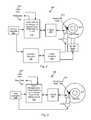
- FIG. 2shows a storage system including a read channel circuit with an inter-track interference based track width setting circuit in accordance with some embodiments of the present invention
- FIG. 3shows a read head characterization test station including a head characterization circuit with an inter-track interference based track width setting circuit in accordance with some embodiments of the present invention
- FIG. 4depicts an inter-track interference based track width setting circuit in accordance with one or more embodiments of the present invention
- FIGS. 5 a - 5 cdepict example interim outputs relative to track width settings in accordance with some embodiments of the present invention.
- FIG. 6is a flow diagram of a method in accordance with some embodiments of the present invention for track width setting.
- the present inventionsare related to systems and methods sensing data, and more particularly to systems and methods for characterizing a data sensor.
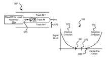
- FIG. 1a storage medium 1 is shown with two example tracks 20 , 22 indicated as dashed lines.
- the tracksare segregated by servo data written within wedges 19 , 18 .
- These wedgesinclude servo data that are used for control and synchronization of a read/write head assembly over a desired location on storage medium 1 .
- User datais stored in the regions between the wedges. It should be noted that while two tracks and two wedges are shown, hundreds of each would typically be included on a given storage medium.
- FIG. 1 bshows three adjacent tracks (Track N ⁇ 1, Track N, and Track N+1) with a read/write head assembly 60 flying in a direction 70 over Track N.
- read/write head assembly 60will sense the data written to either or both of Track N ⁇ 1 and Track N+1 in addition to the data written to Track N. Conversely, where the width of Track N is very wide, a properly located read/write head assembly 60 will not sense substantially sense the data written to either or both of Track N ⁇ 1 and Track N+1.
- Various embodiments of the present inventionare tailored to properly define the width of the tracks to optimize track width to increase storage density (i.e., decreasing width) in balance with minimizing interference with adjacent tracks (i.e., increasing width).
- Storage system 200may be, for example, a hard disk drive.
- Storage system 200also includes a preamplifier 270 , an interface controller 220 , a hard disk controller 266 , a motor controller 268 , a spindle motor 272 , a disk platter 278 , and a read/write head assembly 276 .
- Interface controller 220controls addressing and timing of data to/from disk platter 278 .
- the data on disk platter 278consists of groups of magnetic signals that may be detected by read/write head assembly 276 when the assembly is properly positioned over disk platter 278 .
- disk platter 278includes magnetic signals recorded in accordance with either a longitudinal or a perpendicular recording scheme.
- read/write head assembly 276is accurately positioned by motor controller 268 over a desired data track on disk platter 278 .
- the desired trackis identified in part using the enhanced servo data processing circuit.
- Motor controller 268both positions read/write head assembly 276 in relation to disk platter 278 and drives spindle motor 272 by moving read/write head assembly to the proper data track on disk platter 278 under the direction of hard disk controller 266 .
- Spindle motor 272spins disk platter 278 at a determined spin rate (RPMs). Once read/write head assembly 276 is positioned adjacent the proper data track, magnetic signals representing data on disk platter 278 are sensed by read/write head assembly 276 as disk platter 278 is rotated by spindle motor 272 .
- RPMsspin rate
- the sensed magnetic signalsare provided as a continuous, minute analog signal representative of the magnetic data on disk platter 278 .
- This minute analog signalis transferred from read/write head assembly 276 to read channel module 264 via preamplifier 270 .
- Preamplifier 270is operable to amplify the minute analog signals accessed from disk platter 278 .
- read channel circuit 210decodes and digitizes the received analog signal to recreate the information originally written to disk platter 278 .
- This datais provided as read data 203 to a receiving circuit.
- a write operationis substantially the opposite of the preceding read operation with write data 201 being provided to read channel circuit 210 . This data is then encoded and written to disk platter 278 .
- the width of the tracks being written and read by read/write head assembly 276is variable, and may be varied based upon an amount of inter-track interference sensed by read/write head assembly 276 .
- the amount of interferenceis determined by and the track width modified by the inter-track interference based track width setting circuit included as part of read channel circuit 210 .
- the inter-track interference based track width setting circuitmay be implemented similar to that described below in relation to FIG. 4 and/or using the approach discussed below in relation to FIG. 6 .
- storage system 200may be integrated into a larger storage system such as, for example, a RAID (redundant array of inexpensive disks or redundant array of independent disks) based storage system. It should also be noted that various functions or blocks of storage system 200 may be implemented in either software or firmware, while other functions or blocks are implemented in hardware.
- RAIDredundant array of inexpensive disks or redundant array of independent disks
- Test station 300including a head characterization circuit with an inter-track interference based track width setting circuit is shown in accordance with some embodiments of the present invention.
- Test station 300also includes a preamplifier 370 , an test controller 320 , a test disk 378 , and a read head under test 376 .
- Test controller 320controls the width of tracks written to test disk 378 , the spin of test disk 378 relative to read head 376 , and the location of read head 376 relative to test disk 378 .
- test controller 320In operation, data is written to tracks on test disk 378 that exhibit a width controlled by test controller 320 (i.e., test controller 32 controls the radial location of read head 376 during writes to test disk 378 ). Test controller 320 then positions read head 376 over a track to be read.
- the data on test disk 378consists of groups of magnetic signals that may be detected by read head 376 when the assembly is properly positioned over disk platter 378 .
- read head 376senses the data and transfers minute analog signals representative of the data to head characterization circuit 310 via preamplifier circuit 370 .
- Preamplifier 270is operable to amplify the minute analog signals accessed from test disk 378 .
- head characterization circuit 310determines an amount of interference caused by tracks adjacent to that being read. This process is repeated for different track widths under the control of test controller 320 until a read width of read head 376 is established. This read width is provided as a characteristic of read head 376 . The amount of interference is determined by and guidance on modifying the track width is provided the inter-track interference based track width setting circuit included as part of head characterization circuit 310 .
- the inter-track interference based track width setting circuitmay be implemented similar to that described below in relation to FIG. 4 and/or using the approach discussed below in relation to FIG. 6 .
- Setting circuit 400includes a write data controller circuit 416 that is operable to format and write a data pattern received as data input 414 to a disk platter 478 using a read/write head assembly 476 .
- Write data controller circuit 416is provided to read/write head assembly 476 as write data 418 .
- Write data controller circuit 416may be any circuit known in the art that is capable of formatting a data set to be provided to a read/write head assembly for writing to a storage medium.
- setting circuit 400includes a track width register 406 that stores a track width input 404 , and provides the stored track width as a track width output 408 to a head location and disk rotation controller circuit 410 .
- Head location and disk rotation controller circuit 410is shown in dashed lines as it may include a number of elements including, but not limited to, a hard disk controller, a motor controller, and/or a spindle motor similar to those discussed above in relation to FIG. 2 .
- Head location and disk rotation controller circuit 410is operable to position read/write head assembly 476 relative to disk platter 478 and to control the rotation of disk platter 478 relative to read/write head assembly 476 using a control output 412 .
- read/write head assembly 476In controlling the position of read/write head assembly 476 relative to disk platter 478 , read/write head assembly 476 is positioned a distance away from a previous track that corresponds to track width output 408 .
- head location and disk rotation controller circuit 410receives a head offset control value 420 that controls an offset from an expected track centerline. In particular, in positioning read/write head assembly 476 relative to disk platter 478 , head location and disk rotation controller circuit 410 adjusts the location of read/write head assembly 476 a positive or negative offset from the location set by track width output 408 .
- Setting circuit 400also includes an analog front end circuit 434 that receives an analog signal 430 from read/write head assembly 476 during read operations, and provides a corresponding analog output signal 436 .
- Analog front end circuit 434may include any circuitry known in the art that is capable of receiving an analog input signal and providing a modified analog signal as an output.
- analog front end circuit 434includes an amplifier (not shown) that receives and amplifies analog input signal 430 and an analog filter (not shown) that reduces any noise exhibited at the output of the amplifier. Based upon the disclosure provided herein, one of ordinary skill in the art will recognize a variety of circuitry that may be included in analog front end circuit 434 in accordance with different embodiments of the present invention.
- Analog output signal 436is provided to an analog to digital converter circuit 438 .
- Analog to digital converter circuit 438provides a series of digital samples 440 representing analog output signal 436 .
- Digital samples 440are synchronized to a sample clock (not shown) that is provided to analog to digital converter circuit 438 .
- Analog to digital converter circuit 438may be any circuit or system known in the art that is capable of converting a continuous signal into a series of digital samples.
- Analog input signal 436is a continuous signal representing a number of bit periods. The bit periods recur with a periodicity of T, and the sample clock causes analog to digital converter circuit 438 to generate a number of samples of analog input signal 430 for each period T. In one particular embodiment of the present invention, four samples are generated for each period T.
- each period Teight samples are generated for each period T. It should be noted that other numbers of samples per period may be generated. Based upon the disclosure provided herein, one of ordinary skill in the art will recognize a variety of sampling frequencies and corresponding bit periods that may be used in relation to different embodiments of the present invention.
- Digital samples 440are provided to a track width controller circuit 402 , and track width controller circuit 402 provides track width input 404 to track width register 406 , and data input 414 to write controller circuit 416 .
- Track width controller circuit 402is operable to perform a stepwise approach to determining a track width on disk platter 478 that optimizes the operation of the read element included in read/write head assembly 476 .
- track width controller circuit 402sets an initial track width by writing a value corresponding to the initial track width to track width register 406 .
- track location controller circuit 402provides an adjacent data pattern as data input 414 to write data controller circuit 416 that in turn causes a signal corresponding to data input 414 to be stored to disk platter 478 via read/write head assembly 476 .
- adjacent trackis used in its broadest sense to mean a location on a storage medium that is adjacent to another location that will be the target of a read (i.e., a target track”).
- Track N ⁇ 1 and Track N+1 of FIG. 1 bare respectively adjacent tracks.
- target trackis a location on a storage medium that is the target of a read operation.
- Track N of FIG. 1 bis a target track as read/write head assembly 60 is positioned to interact with Track N.
- a given trackmay in one instance be a “target track” when it is being read, and in another instance be an “adjacent track” when a track adjacent to the given track is being read.
- Head location and disk rotation controller circuit 410additionally causes read/write head assembly 476 to position over a target track next to the previously discussed adjacent track and also having a track width corresponding to track width output 408 , track location controller circuit 402 provides a target data pattern as data input 414 to write data controller circuit 416 that in turn causes a signal corresponding to data input 414 to be stored to disk platter 478 via read/write head assembly 476 .
- target data patternand “adjacent data pattern” are used in their broadest senses to mean any data pattern distinguishable from the other (i.e., a target data pattern is any data pattern that is distinguishable from an adjacent data pattern, and vice versa).
- an adjacent data patternmay be a series of data that causes relatively high values to be written to disk platter 478 and a corresponding target data pattern may be a series of data that causes relatively low values to be written to disk platter 478 .
- head location and disk rotation controller circuit 410causes read/write head assembly 476 to position over another adjacent track next to the previously discussed target track and also having a track width corresponding to track width output 408 .
- track location controller circuit 402provides an adjacent data pattern as data input 414 to write data controller circuit 416 that in turn causes a signal corresponding to data input 414 to be stored to disk platter 478 via read/write head assembly 476 .
- track width controller circuit 402causes write controller circuit 410 to position read/write head assembly 476 over the target track with an offset from the centerline of the target track defined by an initial offset value provided by track width controller circuit 402 as head offset control value 420 .
- the initial offsetis set to make interference from one of the adjacent tracks likely (i.e., read/write head assembly 476 is positioned far enough from the center line of the target track such that it senses both the target track and the adjacent track on the side of the target track corresponding to the offset).
- read/write head assembly 476senses the previously stored target data and provides the sensed information as analog signal 430 .
- digital samples 440 corresponding to analog signal 430are provided to track width control circuit 402 .
- Track width control circuitanalyzes digital samples 403 to determine if there is any impact from the adjacent track on the side of target track corresponding to the offset.
- the offset value provided by track width controller circuit 402 as head offset control value 420is adjusted such that read/write head assembly 476 moves stepwise away from the adjacent track from which the interference is sensed. This stepwise process is continued until the interference from the adjacent track drops below a threshold level.
- the threshold levelmay be programmable.
- the offset corresponding to the step where the interference the adjacent track drops below a threshold levelis identified as a first non-interference point.
- the stepwise process of adjusting the offset value provided by track width controller circuit 402 as head offset control value 420is continued until interference from the adjacent track on the opposite side of the target track exceeds the threshold level.
- non-interference pointis used in its broadest sense to mean a point where interference from an adjacent track is less than or equal to a given level or percentage.
- FIG. 5 aThe previously described case is graphically depicted in FIG. 5 a where a read/write head assembly 560 is shown in relation to a target track (Track N), and two adjacent tracks (Track N ⁇ 1 and Track N+1). Each of the tracks are set to have a width 573 that may be set by track width controller circuit 402 by writing track width register 406 .
- Read/write head assemblyhas a read width 580 . Read/write head assembly may be offset in both a positive direction 572 and a negative direction 574 from a centerline 570 of the target track under the control of track width controller circuit 402 via head offset control value 420 .
- a graph 510shows the change in signal level (i.e., digital samples 440 ) as head offset control value 420 is varied from an extreme positive direction 572 from centerline 570 to an extreme negative direction 574 from centerline 570 .
- the signal leveldrops below a threshold level at a first non-interference point 591 , and again exceeds the threshold level at a second non-interference point 593 .
- the first and second non-interference pointsmay be on either side of centerline 570 . In this case, the distance between first non-interference point 591 and second non-interference point 593 is significant suggesting that the width of the tracks may be decreased for this particular read/write head assembly.
- graph 510suggest that the values written to the adjacent tracks are high relative to the values written to the target track. The reverse is also possible where the values written to the adjacent tracks is relatively low compared with those written to the target track. Such a case can be accommodated by changing the threshold level and detecting a greater than condition rather than a less than condition. It should be noted that one of the adjacent tracks may be relatively higher than the target track, and the other adjacent track may be relatively lower than the target track with a corresponding change in threshold levels and logic.
- track width controller circuit 402calculates the distance between the first non-interference and the second non-interference point. This distance is then compared with an acceptable range. Where the distance is too small there is an undue interference from adjacent tracks for a given read/write head assembly. In contrast, where the distance is too large the density of storage supported by the given read/write head assembly is less than possible. Where the distance is too small, track width controller circuit 402 increases the width of the tracks by modifying the track width value maintained in track width register 406 , and repeats the process of writing the adjacent and target tracks followed by the previously described stepwise read of the target track.
- track width controller circuit 402decreases the width of the tracks by modifying the track width value maintained in track width register 406 , and repeats the process of writing the adjacent and target tracks followed by the previously described stepwise read of the target track. This process is repeated until an acceptable track width is identified. Once identified, the track width maintained in track width register 406 is used for operation in the case where setting circuit 400 is implemented as part of a storage device, or the track width maintained in track width register 406 is used to characterize read/write head assembly 476 where setting circuit 400 is implemented as part of a test or characterization stand.
- FIG. 5 bshows an example situation where the distance between non-interference points is acceptable.
- the trackshave a width of 571 resulting in a first non-interference point 595 nearer to a second non-interference point 597 than what occurred in graph 510 .
- FIG. 5 cshows an example situation where the distance between non-interference points is too small (i.e., less than zero).
- the trackshave a width of 572 resulting in an inability to detect non-interference point.
- the non-interference pointsare not detected because the interference from one adjacent track is not sufficiently attenuated before the interference from the opposite adjacent track begins to increase.
- a flow diagram 600depicts a method in accordance with some embodiments of the present invention for track width setting.
- an initial track widthis selected (block 605 ). This may be done, for example, by writing an initial track width to a track width register.
- An adjacent track(Track N ⁇ 1) is then written with a defined pattern (block 610 ). In some cases, the defined pattern is an adjacent pattern as described above.
- a target track(Track N) is written with a defined pattern (block 615 ). In some cases, the defined pattern is a target pattern as described above.
- Another adjacent track (Track N+1)is also written with a defined pattern (block 620 ). In some cases, the defined pattern is an adjacent pattern as described above.
- the read/write head assemblyis positioned over the target track (Track N) with an initial offset in a positive direction from the center of the target track (block 625 ). Such positioning may be done in part by providing an initial offset to a write controller circuit. In some cases, the initial offset is selected to be sufficient to assure interference from one of the adjacent tracks (e.g., Track N ⁇ 1). Data is then read from the target track by passing the read/write head assembly over the track as the selected offset to yield a data output (block 630 ). It is determined whether the data output is affected by the defined pattern maintained in the adjacent track (e.g., Track N ⁇ 1) (block 635 ). This may be determined by comparing the data output with a threshold level.
- the data outputmay be considered interfered with by the defined pattern in the adjacent track.
- the offsetis modified in a negative direction (decreasing the positive offset or increasing a negative offset) from the center of the target track, and the read/write head assembly is aligned with the updated offset (block 645 ).
- the processes of blocks 630 - 665are repeated for the updated offset.
- the data outputis not affected by the defined pattern maintained in the adjacent track (e.g., Track N ⁇ 1) (block 635 ) (block 635 )
- the offsetis modified in a positive direction (i.e., to increase a positive offset or decrease a negative offset) from the center of the target track, and the read/write head assembly is aligned with the updated offset (block 650 ).
- the processes of blocks 630 - 665are repeated for the updated offset.
- the target trackwas previously affected by the same adjacent track (block 640 )
- the offsetis identified as a center region or area (i.e., an area with limited or no interference from adjacent tracks), the offset is modified in a negative direction (decreasing the positive offset or increasing a negative offset) from the center of the target track, and the read/write head assembly is aligned with the updated offset (block 660 ).
- the processes of blocks 630 - 665are repeated for the updated offset.
- the extent of the center area or non-interference regionhas been determined and a width of the center area is calculated by subtracting a point corresponding to one extreme of the center area from a point corresponding from the other extreme of the center area (block 665 ).
- it is determined whether the calculated width is too large(block 670 ). This may be done, for example, by comparing the calculated width to threshold value. A calculated width that is too large indicates a lower storage density (i.e., too wide of tracks) than can be supported by the read/write head assembly.
- the track widthis decreased (block 675 ). This may be done, for example, by writing a reduced value to the track width register.
- the processes of blocks 610 - 690are repeated for the updated track width.
- the track widthis not determined to be too large (block 670 ). It is determined whether the calculated width is too small (block 680 ). Again, this may be done, for example, by comparing the calculated width to threshold value. A calculated width that is too small indicates a storage density that is too great (i.e., too narrow of tracks) than can be supported by the read/write head assembly. Where the calculated width is too small (block 680 ), the track width is increased (block 685 ). This may be done, for example, by writing an increased value to the track width register. At this juncture, the processes of blocks 610 - 690 are repeated for the updated track width. Alternatively, where the calculated width is not too small (block 680 ), the calculated track width is stored (block 690 ). This stored track width may be used for operation of a storage device where the method is implemented in relation to a storage device, or may be used to characterize a read head where the method is implemented in relation to a test stand.
- Such integrated circuitsmay include all of the functions of a given block, system or circuit, or only a subset of the block, system or circuit. Further, elements of the blocks, systems or circuits may be implemented across multiple integrated circuits. Such integrated circuits may be any type of integrated circuit known in the art including, but are not limited to, a monolithic integrated circuit, a flip chip integrated circuit, a multichip module integrated circuit, and/or a mixed signal integrated circuit. It should also be noted that various functions of the blocks, systems or circuits discussed herein may be implemented in either software or firmware. In some such cases, the entire system, block or circuit may be implemented using its software or firmware equivalent. In other cases, the one part of a given system, block or circuit may be implemented in software or firmware, while other parts are implemented in hardware.
- the inventionprovides novel systems, devices, methods and arrangements for characterizing read sensors and/or for setting track width. While detailed descriptions of one or more embodiments of the invention have been given above, various alternatives, modifications, and equivalents will be apparent to those skilled in the art without varying from the spirit of the invention. Therefore, the above description should not be taken as limiting the scope of the invention, which is defined by the appended claims.
Landscapes
- Engineering & Computer Science (AREA)
- Signal Processing (AREA)
- Digital Magnetic Recording (AREA)
Abstract
Description
Claims (20)
Priority Applications (1)
| Application Number | Priority Date | Filing Date | Title |
|---|---|---|---|
| US13/100,063US8854752B2 (en) | 2011-05-03 | 2011-05-03 | Systems and methods for track width determination |
Applications Claiming Priority (1)
| Application Number | Priority Date | Filing Date | Title |
|---|---|---|---|
| US13/100,063US8854752B2 (en) | 2011-05-03 | 2011-05-03 | Systems and methods for track width determination |
Publications (2)
| Publication Number | Publication Date |
|---|---|
| US20120281304A1 US20120281304A1 (en) | 2012-11-08 |
| US8854752B2true US8854752B2 (en) | 2014-10-07 |
Family
ID=47090060
Family Applications (1)
| Application Number | Title | Priority Date | Filing Date |
|---|---|---|---|
| US13/100,063Expired - Fee RelatedUS8854752B2 (en) | 2011-05-03 | 2011-05-03 | Systems and methods for track width determination |
Country Status (1)
| Country | Link |
|---|---|
| US (1) | US8854752B2 (en) |
Cited By (14)
| Publication number | Priority date | Publication date | Assignee | Title |
|---|---|---|---|---|
| US20160148630A1 (en)* | 2014-11-24 | 2016-05-26 | Seagate Technology Llc | Adjacent track interference asymmetry mitigation |
| US9524743B2 (en) | 2014-11-24 | 2016-12-20 | Seagate Technology Llc | Heat assisted magnetic recording for bit-patterned media |
| US9583131B1 (en)* | 2015-11-30 | 2017-02-28 | Kabushiki Kaisha Toshiba | Magnetic disk device and control method |
| US9601154B2 (en) | 2014-11-24 | 2017-03-21 | Seagate Technology Llc | Prioritized random access for magnetic recording |
| US9672851B1 (en) | 2016-05-04 | 2017-06-06 | Seagate Technology Llc | Single writer interlaced magnetic recording |
| US9679601B2 (en) | 2014-11-24 | 2017-06-13 | Seagate Technology Llc | Post-write scan operations for interlaced magnetic recording |
| US9747942B2 (en) | 2014-11-24 | 2017-08-29 | Seagate Technology Llc | Variable written track widths for attribute-based storage |
| US9773517B2 (en) | 2014-11-24 | 2017-09-26 | Seagate Technology Llc | Dual writer head design |
| US9805744B1 (en) | 2016-04-01 | 2017-10-31 | Seagate Technology Llc | Dual writer design in interlaced magnetic recording |
| US9805741B1 (en) | 2016-01-29 | 2017-10-31 | Seagate Technology Llc | Write current parameter selection for magnetic recording |
| US9818445B2 (en) | 2016-01-12 | 2017-11-14 | Seagate Technology Llc | Magnetic storage device readers |
| US9842047B2 (en) | 2014-11-24 | 2017-12-12 | Seagate Technology Llc | Non-sequential write for sequential read back |
| US10199066B1 (en) | 2018-03-01 | 2019-02-05 | Seagate Technology Llc | Write management of physically coupled storage areas |
| US10210891B1 (en) | 2016-01-28 | 2019-02-19 | Seagate Technology Llc | Dual writer head design utilizing two writers of different sizes for writing interlaced data tracks |
Families Citing this family (8)
| Publication number | Priority date | Publication date | Assignee | Title |
|---|---|---|---|---|
| US9158634B2 (en)* | 2011-05-19 | 2015-10-13 | Hewlett-Packard Development Company, L.P. | Error control coding |
| JP5793474B2 (en)* | 2012-07-26 | 2015-10-14 | 株式会社東芝 | Recording / reproducing apparatus and recording / reproducing method |
| US9025263B2 (en)* | 2013-08-05 | 2015-05-05 | HGST Netherlands B.V. | Write current and fly height adjustment for compensating media coercivity variation |
| US8941943B1 (en) | 2013-12-09 | 2015-01-27 | HGST Netherlands B.V. | Dynamic variable capacity hard disk drive |
| US8922925B1 (en) | 2013-12-09 | 2014-12-30 | HGST Netherlands B.V. | Actively written guard bands in a cold storage or mixed mode drive |
| US8867153B1 (en)* | 2013-12-09 | 2014-10-21 | HGST Netherlands B.V. | Method and apparatus for dynamic track squeeze in a hard drive |
| US9489145B2 (en) | 2013-12-09 | 2016-11-08 | HGST Netherlands B.V. | Disk drive including I-regions having configurable final logical block addresses |
| JP7170583B2 (en)* | 2019-05-17 | 2022-11-14 | 株式会社東芝 | Magnetic recording device and its magnetic head control method |
Citations (83)
| Publication number | Priority date | Publication date | Assignee | Title |
|---|---|---|---|---|
| JPS53105123A (en)* | 1978-03-17 | 1978-09-13 | Sony Corp | Recording regenerative method for information signal |
| US4991026A (en)* | 1987-09-21 | 1991-02-05 | Hitachi, Ltd. | Chrominance signal reproducing apparatus for video tape recorder |
| US5262904A (en) | 1991-01-22 | 1993-11-16 | International Business Machines Corporation | Method and apparatus for measuring and compensating nonlinear bitshift |
| US5357520A (en) | 1992-01-31 | 1994-10-18 | International Business Machines Corporation | Method and apparatus for precompensation value determination in a PRML data channel |
| US5493454A (en) | 1994-10-04 | 1996-02-20 | Quantum Corporation | Write precompensation optimization in a PRML channel using a selected PRML signal level |
| US5517146A (en) | 1994-04-18 | 1996-05-14 | Silicon Systems, Inc. | Write precompensation circuit for compensating nonlinear magnetic effects in a recording channel |
| GB2320866A (en) | 1996-12-30 | 1998-07-01 | Daewoo Electronics Co Ltd | An equalization arrangement in which initial values which determine tap coefficients are adaptively chosen |
| US5781358A (en) | 1995-07-31 | 1998-07-14 | Nec Corporation | Magnetic recording apparatus with non-linear bit shift measurement |
| US5872664A (en) | 1996-12-06 | 1999-02-16 | Phase Metrics, Inc. | Distortion of an isolated pulse |
| US5986830A (en) | 1997-07-30 | 1999-11-16 | Cirrus Logic, Inc. | Read/write channel write precompensation system and method using one or more delay clocks |
| US5999355A (en) | 1996-04-30 | 1999-12-07 | Cirrus Logic, Inc. | Gain and phase constrained adaptive equalizing filter in a sampled amplitude read channel for magnetic recording |
| US6043942A (en) | 1997-10-09 | 2000-03-28 | International Business Machines Corporation | Selectable write precompensation in a direct access storage device (DASD) |
| US6091560A (en) | 1997-10-30 | 2000-07-18 | Seagate Technology, Inc. | Low frequency signal baseline shift compensation in a disc drive |
| US6130794A (en) | 1998-06-30 | 2000-10-10 | Lucent Technologies Inc. | Statistical monitoring of data channels for enhanced data recovery performance |
| US6134691A (en) | 1998-02-27 | 2000-10-17 | Agilent Technologies, Inc. | NLTS correction circuit |
| US6141168A (en) | 1995-04-21 | 2000-10-31 | Fujitsu Limited | Automatic calibration method, read apparatus and storage apparatus |
| US6147828A (en) | 1998-03-04 | 2000-11-14 | Texas Instruments Incorporated | Method and apparatus for reducing asymmetry in a signal from a magneto-resistive read head |
| US6181505B1 (en) | 1998-06-26 | 2001-01-30 | Seagate Technology Llc | Synchronous digital demodulator with integrated read and servo channels |
| US6208477B1 (en) | 1997-06-06 | 2001-03-27 | Western Digital Corporation | Hard disk drive having a built-in self-test for measuring non-linear signal distortion |
| US6212024B1 (en) | 1997-05-30 | 2001-04-03 | Hitachi, Ltd. | Recording equalizer and magnetic recording/reproducing apparatus performing write timing compensation |
| US6243031B1 (en) | 1998-05-20 | 2001-06-05 | Marvell International Ltd. | Selectable delay circuit having immunity to variations in fabrication and operating condition for write precompensation in a read/write channel |
| US6246723B1 (en) | 1998-05-04 | 2001-06-12 | Cirrus Logic, Inc. | Sampled amplitude read channel employing early-decisions from a trellis sequence detector for sampling value estimation |
| US6337778B1 (en) | 1999-05-25 | 2002-01-08 | Western Digital Technologies, Inc. | Disk drive employing vector addition of primary phase write clock signals for generating secondary phase write clock signal |
| US6396651B1 (en) | 1999-07-12 | 2002-05-28 | Deanne S. Grover | Gear-shifting compensation system and method for nonlinear input elements |
| US6404572B1 (en) | 1999-05-05 | 2002-06-11 | Texas Instruments Incorporated | Circuit and method for generating a write precompensation signal |
| DE10127447C1 (en) | 2001-06-07 | 2002-10-10 | Infineon Technologies Ag | Digital processing of analog data stream involves computing sampling time for sampling clock signal depending on phase control signal derived from analog signal and defined clock signal. |
| US20030026354A1 (en) | 2001-08-01 | 2003-02-06 | Via Technologies, Inc. | Receiver and the compensation method therefor |
| US6535345B1 (en) | 1999-07-21 | 2003-03-18 | Fujitsu Limited | Signal processing apparatus and signal processing method |
| US6563655B1 (en) | 1996-05-20 | 2003-05-13 | Texas Instruments Incorporated | Method and apparatus for failsafing and extending range for write precompensation |
| US6621648B2 (en) | 2001-04-30 | 2003-09-16 | Agere Systems Inc. | Look ahead write precompensation |
| US6661627B1 (en)* | 1999-10-19 | 2003-12-09 | Matsushita Electric Industrial Co., Ltd. | Magnetic recording device, method of adjusting magnetic head, and magnetic recording medium |
| US6662303B1 (en) | 2000-01-10 | 2003-12-09 | Infineon Technologies North America Corp. | Write precompensation circuit and read channel with write precompensation circuit that generates output signals by interpolating between selected phases |
| US6671244B2 (en) | 1999-12-24 | 2003-12-30 | Nec Corporation | Information detecting circuit including adaptive equalizer and reproducing apparatus |
| US6674590B2 (en) | 1998-12-02 | 2004-01-06 | Hitachi Global Technologies | System and method for estimating a frequency of slider airbearing resonance |
| US6678230B2 (en) | 2000-10-31 | 2004-01-13 | Matsushita Electric Industrial Co., Ltd. | Waveform equalizer for a reproduction signal obtained by reproducing marks and non-marks recorded on a recording medium |
| US6721114B1 (en) | 2001-05-09 | 2004-04-13 | Marvell International, Ltd. | Precompensation circuit for magnetic recording |
| US6788481B2 (en) | 2002-03-21 | 2004-09-07 | International Business Machines Corporation | Process for measuring nonlinear transition shift (NLTS) at high recording densities with a giant magetoresistive (GMR) head |
| US6894854B1 (en) | 1996-12-12 | 2005-05-17 | Maxtor Corporation | Disk drive which detects head flying height using first and second non-overlapping data patterns with different frequencies |
| US20050117243A1 (en) | 2003-10-31 | 2005-06-02 | Orimitsu Serizawa | Adaptive equalizer |
| US6912682B1 (en) | 1999-09-10 | 2005-06-28 | Matsushita Electric Industrial Co., Ltd. | Signal processor for correcting and detecting errors |
| US20050169415A1 (en) | 2004-01-30 | 2005-08-04 | Agere Systems Inc. | Timing error recovery system |
| US6934100B2 (en) | 2000-11-30 | 2005-08-23 | Fujitsu Limited | Method of measuring non-linearity in magnetic recording/reproduction, device for magnetic recording/reproduction and LSI for magnetic recording reproduction |
| US6937415B2 (en) | 2002-02-04 | 2005-08-30 | Hitachi Global Storage Technologies Netherlands B.V. | Method and apparatus for enhanced data channel performance using read sample buffering |
| US7012772B1 (en) | 1998-09-02 | 2006-03-14 | Cirrus Logic, Inc. | Sampled amplitude read channel employing an adaptive non-linear correction circuit for correcting non-linear distortions in a read signal |
| US20060061496A1 (en) | 2004-09-20 | 2006-03-23 | Stein Anatoli B | Self-adjusting PRML receiver |
| US20060062125A1 (en) | 2003-07-18 | 2006-03-23 | Mitsubishi Chemical Corporation | Optical recording method |
| US7079342B1 (en) | 2004-07-26 | 2006-07-18 | Marvell International Ltd. | Method and apparatus for asymmetry correction in magnetic recording channels |
| US20060176947A1 (en) | 2005-02-07 | 2006-08-10 | Samsung Electronics Co., Ltd. | Apparatus and method for setting tap coefficient of adaptive equalizer |
| US7092179B2 (en) | 2001-07-06 | 2006-08-15 | Fujitsu Limited | Write precompensation amount setting method and apparatus |
| US7092180B2 (en) | 2004-04-01 | 2006-08-15 | Agere Systems Inc. | Asymmetry correction for magneto-resistive heads |
| US7123429B2 (en) | 2004-02-26 | 2006-10-17 | Hitachi Global Storage Technologies Netherlands B.V. | Method and apparatus for providing write pre-compensation using a read timing path |
| US20060232871A1 (en) | 2005-04-13 | 2006-10-19 | Brittenham Steven L | Medium dependent write equalization |
| US7126773B1 (en) | 2005-03-30 | 2006-10-24 | Hitachi Global Storage Technologies Netherlands, B.V. | Write precompensation method for perpendicular magnetic recording |
| US7139143B2 (en) | 1996-05-16 | 2006-11-21 | Hitachi, Ltd. | Disk device and method of generating signal representing head |
| US7170704B2 (en) | 2004-06-25 | 2007-01-30 | Stmicroelectronics, Inc. | Enhanced dibit extraction |
| US7170700B1 (en)* | 2001-04-19 | 2007-01-30 | Maxtor Corporation | Method of determining side track erasure in a disk drive |
| US20070041115A1 (en) | 2005-07-29 | 2007-02-22 | Lee Yuan X | Methods and systems for automatically characterizing non-linearities of a read-back signal of a recording system |
| US20070047120A1 (en) | 2005-08-29 | 2007-03-01 | Degroat Ronald D | Dibit extraction |
| US7193802B2 (en) | 2004-03-25 | 2007-03-20 | Hitachi Global Storage Technologies Netherlands, B.V. | Apparatus for providing dynamic equalizer optimization |
| US20070064836A1 (en) | 2005-09-16 | 2007-03-22 | Agere Systems Inc. | Format efficient timing acquisition for magnetic recording read channels |
| US20070076313A1 (en) | 2005-10-03 | 2007-04-05 | Hutchins Robert A | Dynamic method for asymmetry compensation in a storage read channel |
| US20070140088A1 (en) | 2003-09-30 | 2007-06-21 | Yasumori Hino | Evaluating apparatus and evaluating method |
| US7248424B2 (en) | 2003-04-25 | 2007-07-24 | Fujitsu Limited | Nonlinearity measuring method, nonlinearity measuring unit, magnetic recording/regenerating unit and LSI for magnetic recording/regenerating |
| US7262928B1 (en) | 2003-03-25 | 2007-08-28 | Marvell International Ltd. | Dc-offset compensation loops for magnetic recording system |
| US7271753B1 (en) | 2006-01-18 | 2007-09-18 | Maxtor Corporation | Calibration of analog front end for gain sensitive measurements |
| US20070236270A1 (en) | 2006-04-07 | 2007-10-11 | Innolux Display Corp. | Clock-pulse generator and shift register using the same |
| US7283316B2 (en)* | 2002-01-17 | 2007-10-16 | Maxtor Corporation | Vertical track zoning for disk drives |
| US20070260623A1 (en) | 2006-05-05 | 2007-11-08 | Jaquette Glen A | Apparatus, system, and method for read back verification of stored data |
| US7308057B1 (en) | 2003-06-05 | 2007-12-11 | Maxtor Corporation | Baseline wander compensation for perpendicular recording |
| US20080032652A1 (en) | 2006-08-04 | 2008-02-07 | Samsung Electronics Co., Ltd. | Phase detection apparatus and method, phase locked loop circuit and control method thereof, and signal reproducing apparatus and method |
| US20080031114A1 (en) | 2006-08-01 | 2008-02-07 | Samsung Electronics Co., Ltd. | Read circuit of a disk drive system and method of signal processing thereof |
| US20080037153A1 (en) | 2006-05-08 | 2008-02-14 | Fuji Electric Device Technology Co., Ltd | Characteristic evaluation method for magnetic disk medium |
| US20080081382A1 (en) | 2006-09-28 | 2008-04-03 | Chung-Heng Yang | Method for reducing layout-dependent variations in semiconductor devices |
| US7426236B1 (en) | 2000-08-24 | 2008-09-16 | Marvell International Ltd. | Feedforward equalizer for DFE based detector |
| US7440224B2 (en) | 2006-01-23 | 2008-10-21 | Toshiba Corporation | Disk drive servo |
| US20090033680A1 (en) | 2006-03-15 | 2009-02-05 | Dong-Ki Lee | Apparatuses For Overlaying Images, Portable Devices Having The Same And Methods Of Overlaying Images |
| US7542227B2 (en) | 2007-06-29 | 2009-06-02 | Samsung Electronics Co., Ltd. | Flying height measurement and control with user data signal |
| US20090161245A1 (en) | 2007-12-21 | 2009-06-25 | Lsi Corporation | Frequency Domain Approach for Efficient Computation of Fixed-point Equalization Targets |
| US20090230639A1 (en) | 2005-02-28 | 2009-09-17 | Volkswagen Ag | Method for Operating Active Stabilizers in Motor Vehicles and Motor Vehicle Having Active Stabilizers |
| US7696838B2 (en) | 2004-09-09 | 2010-04-13 | Nec Corporation | Equalizing filter circuit |
| US7715135B1 (en) | 2005-09-20 | 2010-05-11 | Marvell International Ltd. | Methods, circuits, apparatus, and systems for read channel synchronization and/or fly height measurement |
| US7733591B2 (en) | 2006-12-18 | 2010-06-08 | Hitachi Global Storage Technologies Netherlands B.V. | Data storage device with data recovery process using fixed phase clocking for analog-to-digital conversion |
| US8467142B2 (en)* | 2008-10-30 | 2013-06-18 | Sharp Kabushiki Kaisha | Recording medium, recording/reproduction device and method for controlling recording/reproduction device |
- 2011
- 2011-05-03USUS13/100,063patent/US8854752B2/ennot_activeExpired - Fee Related
Patent Citations (87)
| Publication number | Priority date | Publication date | Assignee | Title |
|---|---|---|---|---|
| JPS53105123A (en)* | 1978-03-17 | 1978-09-13 | Sony Corp | Recording regenerative method for information signal |
| US4991026A (en)* | 1987-09-21 | 1991-02-05 | Hitachi, Ltd. | Chrominance signal reproducing apparatus for video tape recorder |
| US5262904A (en) | 1991-01-22 | 1993-11-16 | International Business Machines Corporation | Method and apparatus for measuring and compensating nonlinear bitshift |
| US5357520A (en) | 1992-01-31 | 1994-10-18 | International Business Machines Corporation | Method and apparatus for precompensation value determination in a PRML data channel |
| US5517146A (en) | 1994-04-18 | 1996-05-14 | Silicon Systems, Inc. | Write precompensation circuit for compensating nonlinear magnetic effects in a recording channel |
| US5583705A (en) | 1994-10-04 | 1996-12-10 | Quantum Corporation | Write precompensation optimization in a PRML channel using a selected PRML signal level |
| US5493454A (en) | 1994-10-04 | 1996-02-20 | Quantum Corporation | Write precompensation optimization in a PRML channel using a selected PRML signal level |
| US6141168A (en) | 1995-04-21 | 2000-10-31 | Fujitsu Limited | Automatic calibration method, read apparatus and storage apparatus |
| US5781358A (en) | 1995-07-31 | 1998-07-14 | Nec Corporation | Magnetic recording apparatus with non-linear bit shift measurement |
| US6208481B1 (en) | 1996-04-30 | 2001-03-27 | Cirrus Logic, Inc. | Gain and phase constrained adaptive equalizing filter in a sampled amplitude read channel for magnetic recording |
| US5999355A (en) | 1996-04-30 | 1999-12-07 | Cirrus Logic, Inc. | Gain and phase constrained adaptive equalizing filter in a sampled amplitude read channel for magnetic recording |
| US7139143B2 (en) | 1996-05-16 | 2006-11-21 | Hitachi, Ltd. | Disk device and method of generating signal representing head |
| US6563655B1 (en) | 1996-05-20 | 2003-05-13 | Texas Instruments Incorporated | Method and apparatus for failsafing and extending range for write precompensation |
| US5872664A (en) | 1996-12-06 | 1999-02-16 | Phase Metrics, Inc. | Distortion of an isolated pulse |
| US6894854B1 (en) | 1996-12-12 | 2005-05-17 | Maxtor Corporation | Disk drive which detects head flying height using first and second non-overlapping data patterns with different frequencies |
| GB2320866A (en) | 1996-12-30 | 1998-07-01 | Daewoo Electronics Co Ltd | An equalization arrangement in which initial values which determine tap coefficients are adaptively chosen |
| US6212024B1 (en) | 1997-05-30 | 2001-04-03 | Hitachi, Ltd. | Recording equalizer and magnetic recording/reproducing apparatus performing write timing compensation |
| US6208477B1 (en) | 1997-06-06 | 2001-03-27 | Western Digital Corporation | Hard disk drive having a built-in self-test for measuring non-linear signal distortion |
| US5986830A (en) | 1997-07-30 | 1999-11-16 | Cirrus Logic, Inc. | Read/write channel write precompensation system and method using one or more delay clocks |
| US6043942A (en) | 1997-10-09 | 2000-03-28 | International Business Machines Corporation | Selectable write precompensation in a direct access storage device (DASD) |
| US6091560A (en) | 1997-10-30 | 2000-07-18 | Seagate Technology, Inc. | Low frequency signal baseline shift compensation in a disc drive |
| US6134691A (en) | 1998-02-27 | 2000-10-17 | Agilent Technologies, Inc. | NLTS correction circuit |
| US6147828A (en) | 1998-03-04 | 2000-11-14 | Texas Instruments Incorporated | Method and apparatus for reducing asymmetry in a signal from a magneto-resistive read head |
| US6246723B1 (en) | 1998-05-04 | 2001-06-12 | Cirrus Logic, Inc. | Sampled amplitude read channel employing early-decisions from a trellis sequence detector for sampling value estimation |
| US6243031B1 (en) | 1998-05-20 | 2001-06-05 | Marvell International Ltd. | Selectable delay circuit having immunity to variations in fabrication and operating condition for write precompensation in a read/write channel |
| US6181505B1 (en) | 1998-06-26 | 2001-01-30 | Seagate Technology Llc | Synchronous digital demodulator with integrated read and servo channels |
| US6130794A (en) | 1998-06-30 | 2000-10-10 | Lucent Technologies Inc. | Statistical monitoring of data channels for enhanced data recovery performance |
| US7012772B1 (en) | 1998-09-02 | 2006-03-14 | Cirrus Logic, Inc. | Sampled amplitude read channel employing an adaptive non-linear correction circuit for correcting non-linear distortions in a read signal |
| US6674590B2 (en) | 1998-12-02 | 2004-01-06 | Hitachi Global Technologies | System and method for estimating a frequency of slider airbearing resonance |
| US6404572B1 (en) | 1999-05-05 | 2002-06-11 | Texas Instruments Incorporated | Circuit and method for generating a write precompensation signal |
| US6337778B1 (en) | 1999-05-25 | 2002-01-08 | Western Digital Technologies, Inc. | Disk drive employing vector addition of primary phase write clock signals for generating secondary phase write clock signal |
| US6396651B1 (en) | 1999-07-12 | 2002-05-28 | Deanne S. Grover | Gear-shifting compensation system and method for nonlinear input elements |
| US6535345B1 (en) | 1999-07-21 | 2003-03-18 | Fujitsu Limited | Signal processing apparatus and signal processing method |
| US6912682B1 (en) | 1999-09-10 | 2005-06-28 | Matsushita Electric Industrial Co., Ltd. | Signal processor for correcting and detecting errors |
| US6661627B1 (en)* | 1999-10-19 | 2003-12-09 | Matsushita Electric Industrial Co., Ltd. | Magnetic recording device, method of adjusting magnetic head, and magnetic recording medium |
| US6671244B2 (en) | 1999-12-24 | 2003-12-30 | Nec Corporation | Information detecting circuit including adaptive equalizer and reproducing apparatus |
| US6662303B1 (en) | 2000-01-10 | 2003-12-09 | Infineon Technologies North America Corp. | Write precompensation circuit and read channel with write precompensation circuit that generates output signals by interpolating between selected phases |
| US7426236B1 (en) | 2000-08-24 | 2008-09-16 | Marvell International Ltd. | Feedforward equalizer for DFE based detector |
| US6678230B2 (en) | 2000-10-31 | 2004-01-13 | Matsushita Electric Industrial Co., Ltd. | Waveform equalizer for a reproduction signal obtained by reproducing marks and non-marks recorded on a recording medium |
| US6934100B2 (en) | 2000-11-30 | 2005-08-23 | Fujitsu Limited | Method of measuring non-linearity in magnetic recording/reproduction, device for magnetic recording/reproduction and LSI for magnetic recording reproduction |
| US7170700B1 (en)* | 2001-04-19 | 2007-01-30 | Maxtor Corporation | Method of determining side track erasure in a disk drive |
| US6621648B2 (en) | 2001-04-30 | 2003-09-16 | Agere Systems Inc. | Look ahead write precompensation |
| US6721114B1 (en) | 2001-05-09 | 2004-04-13 | Marvell International, Ltd. | Precompensation circuit for magnetic recording |
| DE10127447C1 (en) | 2001-06-07 | 2002-10-10 | Infineon Technologies Ag | Digital processing of analog data stream involves computing sampling time for sampling clock signal depending on phase control signal derived from analog signal and defined clock signal. |
| US7092179B2 (en) | 2001-07-06 | 2006-08-15 | Fujitsu Limited | Write precompensation amount setting method and apparatus |
| US20030026354A1 (en) | 2001-08-01 | 2003-02-06 | Via Technologies, Inc. | Receiver and the compensation method therefor |
| US7283316B2 (en)* | 2002-01-17 | 2007-10-16 | Maxtor Corporation | Vertical track zoning for disk drives |
| US6937415B2 (en) | 2002-02-04 | 2005-08-30 | Hitachi Global Storage Technologies Netherlands B.V. | Method and apparatus for enhanced data channel performance using read sample buffering |
| US6788481B2 (en) | 2002-03-21 | 2004-09-07 | International Business Machines Corporation | Process for measuring nonlinear transition shift (NLTS) at high recording densities with a giant magetoresistive (GMR) head |
| US7262928B1 (en) | 2003-03-25 | 2007-08-28 | Marvell International Ltd. | Dc-offset compensation loops for magnetic recording system |
| US7248424B2 (en) | 2003-04-25 | 2007-07-24 | Fujitsu Limited | Nonlinearity measuring method, nonlinearity measuring unit, magnetic recording/regenerating unit and LSI for magnetic recording/regenerating |
| US7308057B1 (en) | 2003-06-05 | 2007-12-11 | Maxtor Corporation | Baseline wander compensation for perpendicular recording |
| US20060062125A1 (en) | 2003-07-18 | 2006-03-23 | Mitsubishi Chemical Corporation | Optical recording method |
| US20070140088A1 (en) | 2003-09-30 | 2007-06-21 | Yasumori Hino | Evaluating apparatus and evaluating method |
| US7256954B2 (en) | 2003-10-31 | 2007-08-14 | Sanyo Electric Co., Ltd. | Adaptive equalizer |
| US20050117243A1 (en) | 2003-10-31 | 2005-06-02 | Orimitsu Serizawa | Adaptive equalizer |
| US20050169415A1 (en) | 2004-01-30 | 2005-08-04 | Agere Systems Inc. | Timing error recovery system |
| US7123429B2 (en) | 2004-02-26 | 2006-10-17 | Hitachi Global Storage Technologies Netherlands B.V. | Method and apparatus for providing write pre-compensation using a read timing path |
| US7193802B2 (en) | 2004-03-25 | 2007-03-20 | Hitachi Global Storage Technologies Netherlands, B.V. | Apparatus for providing dynamic equalizer optimization |
| US7092180B2 (en) | 2004-04-01 | 2006-08-15 | Agere Systems Inc. | Asymmetry correction for magneto-resistive heads |
| US7170704B2 (en) | 2004-06-25 | 2007-01-30 | Stmicroelectronics, Inc. | Enhanced dibit extraction |
| US7079342B1 (en) | 2004-07-26 | 2006-07-18 | Marvell International Ltd. | Method and apparatus for asymmetry correction in magnetic recording channels |
| US7696838B2 (en) | 2004-09-09 | 2010-04-13 | Nec Corporation | Equalizing filter circuit |
| US20060061496A1 (en) | 2004-09-20 | 2006-03-23 | Stein Anatoli B | Self-adjusting PRML receiver |
| US20060176947A1 (en) | 2005-02-07 | 2006-08-10 | Samsung Electronics Co., Ltd. | Apparatus and method for setting tap coefficient of adaptive equalizer |
| US20090230639A1 (en) | 2005-02-28 | 2009-09-17 | Volkswagen Ag | Method for Operating Active Stabilizers in Motor Vehicles and Motor Vehicle Having Active Stabilizers |
| US7126773B1 (en) | 2005-03-30 | 2006-10-24 | Hitachi Global Storage Technologies Netherlands, B.V. | Write precompensation method for perpendicular magnetic recording |
| US20060232871A1 (en) | 2005-04-13 | 2006-10-19 | Brittenham Steven L | Medium dependent write equalization |
| US20070041115A1 (en) | 2005-07-29 | 2007-02-22 | Lee Yuan X | Methods and systems for automatically characterizing non-linearities of a read-back signal of a recording system |
| US20070047120A1 (en) | 2005-08-29 | 2007-03-01 | Degroat Ronald D | Dibit extraction |
| US20070064836A1 (en) | 2005-09-16 | 2007-03-22 | Agere Systems Inc. | Format efficient timing acquisition for magnetic recording read channels |
| US7715135B1 (en) | 2005-09-20 | 2010-05-11 | Marvell International Ltd. | Methods, circuits, apparatus, and systems for read channel synchronization and/or fly height measurement |
| US20070076313A1 (en) | 2005-10-03 | 2007-04-05 | Hutchins Robert A | Dynamic method for asymmetry compensation in a storage read channel |
| US7495854B2 (en) | 2005-10-03 | 2009-02-24 | International Business Machines Corporation | Dynamic method for asymmetry compensation in a storage read channel |
| US7271753B1 (en) | 2006-01-18 | 2007-09-18 | Maxtor Corporation | Calibration of analog front end for gain sensitive measurements |
| US7440224B2 (en) | 2006-01-23 | 2008-10-21 | Toshiba Corporation | Disk drive servo |
| US20090033680A1 (en) | 2006-03-15 | 2009-02-05 | Dong-Ki Lee | Apparatuses For Overlaying Images, Portable Devices Having The Same And Methods Of Overlaying Images |
| US20070236270A1 (en) | 2006-04-07 | 2007-10-11 | Innolux Display Corp. | Clock-pulse generator and shift register using the same |
| US20070260623A1 (en) | 2006-05-05 | 2007-11-08 | Jaquette Glen A | Apparatus, system, and method for read back verification of stored data |
| US20080037153A1 (en) | 2006-05-08 | 2008-02-14 | Fuji Electric Device Technology Co., Ltd | Characteristic evaluation method for magnetic disk medium |
| US20080031114A1 (en) | 2006-08-01 | 2008-02-07 | Samsung Electronics Co., Ltd. | Read circuit of a disk drive system and method of signal processing thereof |
| US20080032652A1 (en) | 2006-08-04 | 2008-02-07 | Samsung Electronics Co., Ltd. | Phase detection apparatus and method, phase locked loop circuit and control method thereof, and signal reproducing apparatus and method |
| US20080081382A1 (en) | 2006-09-28 | 2008-04-03 | Chung-Heng Yang | Method for reducing layout-dependent variations in semiconductor devices |
| US7733591B2 (en) | 2006-12-18 | 2010-06-08 | Hitachi Global Storage Technologies Netherlands B.V. | Data storage device with data recovery process using fixed phase clocking for analog-to-digital conversion |
| US7542227B2 (en) | 2007-06-29 | 2009-06-02 | Samsung Electronics Co., Ltd. | Flying height measurement and control with user data signal |
| US20090161245A1 (en) | 2007-12-21 | 2009-06-25 | Lsi Corporation | Frequency Domain Approach for Efficient Computation of Fixed-point Equalization Targets |
| US8467142B2 (en)* | 2008-10-30 | 2013-06-18 | Sharp Kabushiki Kaisha | Recording medium, recording/reproduction device and method for controlling recording/reproduction device |
Non-Patent Citations (28)
| Title |
|---|
| Barry J. et al "Iterative Timing Recovery" IEEE Signal Processing Magazine vol. 21, No. 1, Jan. 1, 2004. |
| Cho and Lee, "An Estimation Technique for Nonlinear Distortion in High Density Magnetic Recording Channels", IEEE Transactions on Magnetics, vol. 34, No. 1, pp. 40-44 Jan. 1998. |
| DeGroat et al., "Experimental Characterization of Media Noise Based on Equalized Synchronized Drive Data", IEEE Trans. Magnetics, vol. 37, No. 2, pp. 633-638, Mar. 2001. |
| Farhang-Boroujeny, Adaptive Filters: Theory and Applications. John Wiley & Sons Ltd, 1998, Chapter 11. pp. 373-379. |
| Kavcic and Patapoutian, "A Signal-Dependent Autoregressive Channel Model", IEEE Trans. Magnetics, vol. 35 No. 5, pp. 2316-2318, Sep. 1999. |
| Lin et al. "An estimation technique for accurately modelling the magnetic recording channel including nonlinearities." IEEE Trans. Mag, vol. 25, No. 5, pp. 4084-4086, Sep. 1989. |
| Moon, J., "Signal-to-Noise Ratio Definition for Magnetic Recording Channels With Transition Noise", IEEE Trans. Magnetics, vol. 36, No. 5, pp. 3881-3883, Sep. 2000. |
| Palmer et al, "Identification of nonlinear write effects using pseudo-random sequences" IEEE Trans. Magnetics, vol. 23 No. 5, pp. 2377-2379, Sep. 1987. |
| Partovi; et al., "Flow-Through Latch and Edge-Triggered Flip-Flop Hybrid Elements"; Feb. 8, 1996; pp. 138-139; Solid-State Circuits Conf Digest of Technical Papers IEEE. |
| Tokumasu et al. "A New Reduced Clock-Swing Flip-Flop (NDKFF)," Corporate Research & Development Center, Toshiba Corporation. IEEE Feb. 2002 Custom Integrated Circuits Conf. |
| U.S. Appl. No. 12/199,325, filed Aug. 27, 2008, Mathew. |
| U.S. Appl. No. 12/247,378, filed Apr. 8, 2010, Mathew. |
| U.S. Appl. No. 12/273,265, filed Nov. 18, 2008, Mathew. |
| U.S. Appl. No. 12/337,775, filed Dec. 18, 2008, Mathew. |
| U.S. Appl. No. 12/337,805, filed Dec. 18, 2008, Mueller. |
| U.S. Appl. No. 12/337,828, filed Dec. 18, 2008, Mueller. |
| U.S. Appl. No. 12/337,850, filed Dec. 18, 2008, Mueller. |
| U.S. Appl. No. 12/348,236, filed Jan. 2, 2009, Liu. |
| U.S. Appl. No. 12/371,906, filed Feb. 16, 2009, Ratnakar Aravind. |
| U.S. Appl. No. 12/430,948, filed Apr. 28, 2009, Grundvig. |
| U.S. Appl. No. 12/463,626, filed May 11, 2009, Mathew. |
| U.S. Appl. No. 12/510,222, filed Jul. 27, 2009, Ratnakar Aravind. |
| U.S. Appl. No. 12/558,928, filed Sep. 14, 2009, Mahtew. |
| U.S. Appl. No. 12/652,201, filed Jan. 5, 2010, Mahtew. |
| U.S. Appl. No. 12/663,325, filed Apr. 20, 2010, Mahtew. |
| U.S. Appl. No. 13/100,063, filed May 3, 2011, Jin, Ming et.al. |
| U.S. Appl. No. 13/180,311, filed Jul. 11, 2011, Tan, Weijun et.al. |
| Wood and Donaldson, "The Helical-Scan Magnetic Tape Recorder as a Digital Communication Channel", IEEE Transactions on Magnetics, vol. MAG-15, No. 2, pp. 935-943 Mar. 1979. |
Cited By (26)
| Publication number | Priority date | Publication date | Assignee | Title |
|---|---|---|---|---|
| US9741364B2 (en) | 2014-11-24 | 2017-08-22 | Seagate Technology Llc | Laser power optimization for heat assisted interlaced magnetic recording |
| US9842047B2 (en) | 2014-11-24 | 2017-12-12 | Seagate Technology Llc | Non-sequential write for sequential read back |
| US9524743B2 (en) | 2014-11-24 | 2016-12-20 | Seagate Technology Llc | Heat assisted magnetic recording for bit-patterned media |
| US9747943B2 (en) | 2014-11-24 | 2017-08-29 | Seagate Technology Llc | Prioritized random access for magnetic recording |
| US9601154B2 (en) | 2014-11-24 | 2017-03-21 | Seagate Technology Llc | Prioritized random access for magnetic recording |
| US9607631B2 (en) | 2014-11-24 | 2017-03-28 | Seagate Technology Llc | Enhanced capacity recording |
| US9633675B2 (en) | 2014-11-24 | 2017-04-25 | Seagate Technology Llc | Interlaced magnetic recording super parity |
| US10049698B2 (en) | 2014-11-24 | 2018-08-14 | Seagate Technology Llc | Interlaced magnetic recording super parity |
| US9672845B2 (en)* | 2014-11-24 | 2017-06-06 | Seagate Technology Llc | Adjacent track interference asymmetry mitigation |
| US9679601B2 (en) | 2014-11-24 | 2017-06-13 | Seagate Technology Llc | Post-write scan operations for interlaced magnetic recording |
| US9728206B2 (en) | 2014-11-24 | 2017-08-08 | Seagate Technology Llc | Interlaced magnetic recording |
| US9741363B2 (en) | 2014-11-24 | 2017-08-22 | Seagate Technology Llc | Laser power optimization for heat assisted interlaced magnetic recording |
| US9508362B2 (en) | 2014-11-24 | 2016-11-29 | Seagate Technology Llc | Write management for interlaced magnetic recording devices |
| US10090016B2 (en) | 2014-11-24 | 2018-10-02 | Seagate Technology Llc | Variable written track widths for attribute-based storage |
| US9858961B2 (en) | 2014-11-24 | 2018-01-02 | Seagate Technology Llc | Reader design for interlaced magnetic recording |
| US9773517B2 (en) | 2014-11-24 | 2017-09-26 | Seagate Technology Llc | Dual writer head design |
| US20160148630A1 (en)* | 2014-11-24 | 2016-05-26 | Seagate Technology Llc | Adjacent track interference asymmetry mitigation |
| US9747942B2 (en) | 2014-11-24 | 2017-08-29 | Seagate Technology Llc | Variable written track widths for attribute-based storage |
| US9583131B1 (en)* | 2015-11-30 | 2017-02-28 | Kabushiki Kaisha Toshiba | Magnetic disk device and control method |
| US9818445B2 (en) | 2016-01-12 | 2017-11-14 | Seagate Technology Llc | Magnetic storage device readers |
| US10210891B1 (en) | 2016-01-28 | 2019-02-19 | Seagate Technology Llc | Dual writer head design utilizing two writers of different sizes for writing interlaced data tracks |
| US9805741B1 (en) | 2016-01-29 | 2017-10-31 | Seagate Technology Llc | Write current parameter selection for magnetic recording |
| US9805744B1 (en) | 2016-04-01 | 2017-10-31 | Seagate Technology Llc | Dual writer design in interlaced magnetic recording |
| US9672851B1 (en) | 2016-05-04 | 2017-06-06 | Seagate Technology Llc | Single writer interlaced magnetic recording |
| US10199066B1 (en) | 2018-03-01 | 2019-02-05 | Seagate Technology Llc | Write management of physically coupled storage areas |
| US10482919B2 (en) | 2018-03-01 | 2019-11-19 | Seagate Technology Llc | Write management of physically coupled storage areas |
Also Published As
| Publication number | Publication date |
|---|---|
| US20120281304A1 (en) | 2012-11-08 |
Similar Documents
| Publication | Publication Date | Title |
|---|---|---|
| US8854752B2 (en) | Systems and methods for track width determination | |
| KR100418740B1 (en) | Method for detecting abnormal magnetic head fly height, method for data writing and hard disk drive apparatus | |
| US8085487B1 (en) | Blocking formats for a disk drive that reduce performance | |
| US7688540B1 (en) | Disk drive selecting TPI profile by estimating head geometry | |
| US8750447B2 (en) | Systems and methods for variable thresholding in a pattern detector | |
| US8189286B1 (en) | Disk drive employing velocity insensitive servo burst pattern | |
| US7633698B2 (en) | Controlling a write inhibit threshold based on vibration | |
| US9013824B1 (en) | Data storage device comprising dual read sensors and dual servo channels to improve servo demodulation | |
| US6226140B1 (en) | Shock detector in a disk drive servo control system | |
| US20150243310A1 (en) | Systems and Methods for Multi-Head Separation Determination | |
| EP2372708B1 (en) | Systems and methods for detecting head contact | |
| US7952825B2 (en) | Method and apparatus adjusting reference clock frequency and disk drive using same | |
| US8941937B1 (en) | Addressing insufficient bit error rates amongst segments | |
| US6215608B1 (en) | Hardware inhibit for a disk drive digital servo control system | |
| US8630055B2 (en) | Systems and methods for medium contact detection | |
| US9245578B1 (en) | Disk drive compensating for inter-track interference in analog read signal | |
| US8300349B2 (en) | Systems and methods for format efficient calibration for servo data based harmonics calculation | |
| US7821734B2 (en) | Head IC, read circuit and medium storage device | |
| US6999261B2 (en) | Magnetic disk device and servo write method | |
| US9053747B1 (en) | Disk drive calibrating failure threshold based on noise power effect on failure detection metric | |
| JP2005346815A (en) | Disk apparatus, head positioning control method, and signal processing circuit | |
| US9825787B1 (en) | Data storage device adapting two-dimensional equalizer based on off-track offset | |
| US8908305B1 (en) | Systems and methods for slider head stability determination | |
| KR20060044791A (en) | Device to provide head amplitude characterization | |
| US8665544B2 (en) | Systems and methods for servo data detection |
Legal Events
| Date | Code | Title | Description |
|---|---|---|---|
| AS | Assignment | Owner name:LSI CORPORATION, CALIFORNIA Free format text:ASSIGNMENT OF ASSIGNORS INTEREST;ASSIGNORS:JIN, MING;XIA, HAITAO;REEL/FRAME:026219/0349 Effective date:20110421 | |
| AS | Assignment | Owner name:AVAGO TECHNOLOGIES GENERAL IP (SINGAPORE) PTE. LTD Free format text:ASSIGNMENT OF ASSIGNORS INTEREST;ASSIGNOR:LSI CORPORATION;REEL/FRAME:035390/0388 Effective date:20140814 | |
| AS | Assignment | Owner name:BANK OF AMERICA, N.A., AS COLLATERAL AGENT, NORTH CAROLINA Free format text:PATENT SECURITY AGREEMENT;ASSIGNOR:AVAGO TECHNOLOGIES GENERAL IP (SINGAPORE) PTE. LTD.;REEL/FRAME:037808/0001 Effective date:20160201 Owner name:BANK OF AMERICA, N.A., AS COLLATERAL AGENT, NORTH Free format text:PATENT SECURITY AGREEMENT;ASSIGNOR:AVAGO TECHNOLOGIES GENERAL IP (SINGAPORE) PTE. LTD.;REEL/FRAME:037808/0001 Effective date:20160201 | |
| AS | Assignment | Owner name:AVAGO TECHNOLOGIES GENERAL IP (SINGAPORE) PTE. LTD., SINGAPORE Free format text:TERMINATION AND RELEASE OF SECURITY INTEREST IN PATENTS;ASSIGNOR:BANK OF AMERICA, N.A., AS COLLATERAL AGENT;REEL/FRAME:041710/0001 Effective date:20170119 Owner name:AVAGO TECHNOLOGIES GENERAL IP (SINGAPORE) PTE. LTD Free format text:TERMINATION AND RELEASE OF SECURITY INTEREST IN PATENTS;ASSIGNOR:BANK OF AMERICA, N.A., AS COLLATERAL AGENT;REEL/FRAME:041710/0001 Effective date:20170119 | |
| FEPP | Fee payment procedure | Free format text:MAINTENANCE FEE REMINDER MAILED (ORIGINAL EVENT CODE: REM.) | |
| LAPS | Lapse for failure to pay maintenance fees | Free format text:PATENT EXPIRED FOR FAILURE TO PAY MAINTENANCE FEES (ORIGINAL EVENT CODE: EXP.); ENTITY STATUS OF PATENT OWNER: LARGE ENTITY | |
| STCH | Information on status: patent discontinuation | Free format text:PATENT EXPIRED DUE TO NONPAYMENT OF MAINTENANCE FEES UNDER 37 CFR 1.362 | |
| FP | Expired due to failure to pay maintenance fee | Effective date:20181007 |