US8853746B2 - CMOS devices with stressed channel regions, and methods for fabricating the same - Google Patents
CMOS devices with stressed channel regions, and methods for fabricating the sameDownload PDFInfo
- Publication number
- US8853746B2 US8853746B2US11/427,495US42749506AUS8853746B2US 8853746 B2US8853746 B2US 8853746B2US 42749506 AUS42749506 AUS 42749506AUS 8853746 B2US8853746 B2US 8853746B2
- Authority
- US
- United States
- Prior art keywords
- semiconductor device
- device structure
- fet
- semiconductor
- layer
- Prior art date
- Legal status (The legal status is an assumption and is not a legal conclusion. Google has not performed a legal analysis and makes no representation as to the accuracy of the status listed.)
- Active, expires
Links
- 238000000034methodMethods0.000titledescription24
- 239000004065semiconductorSubstances0.000claimsabstractdescription241
- 239000013078crystalSubstances0.000claimsabstractdescription65
- 239000000463materialSubstances0.000claimsabstractdescription34
- 230000005669field effectEffects0.000claimsabstractdescription9
- 239000000758substrateSubstances0.000claimsdescription57
- 229910052710siliconInorganic materials0.000claimsdescription45
- 239000010703siliconSubstances0.000claimsdescription42
- 229910000577Silicon-germaniumInorganic materials0.000claimsdescription28
- 239000012212insulatorSubstances0.000claimsdescription22
- 230000001154acute effectEffects0.000claimsdescription18
- 229910021421monocrystalline siliconInorganic materials0.000claimsdescription13
- 239000004020conductorSubstances0.000claimsdescription12
- VYPSYNLAJGMNEJ-UHFFFAOYSA-NSilicium dioxideChemical compoundO=[Si]=OVYPSYNLAJGMNEJ-UHFFFAOYSA-N0.000claimsdescription5
- GWEVSGVZZGPLCZ-UHFFFAOYSA-NTitan oxideChemical compoundO=[Ti]=OGWEVSGVZZGPLCZ-UHFFFAOYSA-N0.000claimsdescription4
- MCMNRKCIXSYSNV-UHFFFAOYSA-NZirconium dioxideChemical compoundO=[Zr]=OMCMNRKCIXSYSNV-UHFFFAOYSA-N0.000claimsdescription4
- 150000001875compoundsChemical class0.000claimsdescription4
- 229910010271silicon carbideInorganic materials0.000claimsdescription4
- 229910001218Gallium arsenideInorganic materials0.000claimsdescription3
- 229910000927Ge alloyInorganic materials0.000claimsdescription3
- 229910000673Indium arsenideInorganic materials0.000claimsdescription3
- 229910003811SiGeCInorganic materials0.000claimsdescription3
- RPQDHPTXJYYUPQ-UHFFFAOYSA-Nindium arsenideChemical compound[In]#[As]RPQDHPTXJYYUPQ-UHFFFAOYSA-N0.000claimsdescription3
- 239000000203mixtureSubstances0.000claimsdescription3
- 229910003465moissaniteInorganic materials0.000claimsdescription3
- 229910021420polycrystalline siliconInorganic materials0.000claimsdescription3
- 229910002244LaAlO3Inorganic materials0.000claimsdescription2
- 229910002370SrTiO3Inorganic materials0.000claimsdescription2
- PNEYBMLMFCGWSK-UHFFFAOYSA-Naluminium oxideInorganic materials[O-2].[O-2].[O-2].[Al+3].[Al+3]PNEYBMLMFCGWSK-UHFFFAOYSA-N0.000claimsdescription2
- 229910052681coesiteInorganic materials0.000claimsdescription2
- 229910052593corundumInorganic materials0.000claimsdescription2
- 229910052906cristobaliteInorganic materials0.000claimsdescription2
- CJNBYAVZURUTKZ-UHFFFAOYSA-Nhafnium(IV) oxideInorganic materialsO=[Hf]=OCJNBYAVZURUTKZ-UHFFFAOYSA-N0.000claimsdescription2
- MRELNEQAGSRDBK-UHFFFAOYSA-Nlanthanum oxideInorganic materials[O-2].[O-2].[O-2].[La+3].[La+3]MRELNEQAGSRDBK-UHFFFAOYSA-N0.000claimsdescription2
- KTUFCUMIWABKDW-UHFFFAOYSA-Noxo(oxolanthaniooxy)lanthanumChemical compoundO=[La]O[La]=OKTUFCUMIWABKDW-UHFFFAOYSA-N0.000claimsdescription2
- 239000000377silicon dioxideSubstances0.000claimsdescription2
- 229910052682stishoviteInorganic materials0.000claimsdescription2
- 229910052905tridymiteInorganic materials0.000claimsdescription2
- 229910001845yogo sapphireInorganic materials0.000claimsdescription2
- LEVVHYCKPQWKOP-UHFFFAOYSA-N[Si].[Ge]Chemical compound[Si].[Ge]LEVVHYCKPQWKOP-UHFFFAOYSA-N0.000claims1
- 229920005591polysiliconPolymers0.000claims1
- 238000005530etchingMethods0.000abstractdescription59
- 230000000295complement effectEffects0.000abstractdescription5
- XUIMIQQOPSSXEZ-UHFFFAOYSA-NSiliconChemical group[Si]XUIMIQQOPSSXEZ-UHFFFAOYSA-N0.000description41
- 238000012545processingMethods0.000description23
- 238000001020plasma etchingMethods0.000description16
- 238000001312dry etchingMethods0.000description7
- KFZMGEQAYNKOFK-UHFFFAOYSA-NIsopropanolChemical compoundCC(C)OKFZMGEQAYNKOFK-UHFFFAOYSA-N0.000description6
- 238000000151depositionMethods0.000description5
- 230000001939inductive effectEffects0.000description5
- 229920002120photoresistant polymerPolymers0.000description5
- 125000006850spacer groupChemical group0.000description5
- 235000012431wafersNutrition0.000description5
- 150000002500ionsChemical class0.000description4
- 238000001039wet etchingMethods0.000description4
- 230000015572biosynthetic processEffects0.000description3
- 229910052799carbonInorganic materials0.000description3
- 238000005229chemical vapour depositionMethods0.000description3
- 239000007789gasSubstances0.000description3
- 238000002513implantationMethods0.000description3
- 238000001459lithographyMethods0.000description3
- 238000000059patterningMethods0.000description3
- HBMJWWWQQXIZIP-UHFFFAOYSA-Nsilicon carbideChemical compound[Si+]#[C-]HBMJWWWQQXIZIP-UHFFFAOYSA-N0.000description3
- 239000000126substanceSubstances0.000description3
- 229910052581Si3N4Inorganic materials0.000description2
- 230000006978adaptationEffects0.000description2
- 230000002411adverseEffects0.000description2
- 238000000231atomic layer depositionMethods0.000description2
- 125000004432carbon atomChemical groupC*0.000description2
- YCIMNLLNPGFGHC-UHFFFAOYSA-NcatecholChemical compoundOC1=CC=CC=C1OYCIMNLLNPGFGHC-UHFFFAOYSA-N0.000description2
- 238000006243chemical reactionMethods0.000description2
- 230000008021depositionEffects0.000description2
- 238000005137deposition processMethods0.000description2
- 239000003989dielectric materialSubstances0.000description2
- 238000011065in-situ storageMethods0.000description2
- 238000010884ion-beam techniqueMethods0.000description2
- 238000002955isolationMethods0.000description2
- 238000000608laser ablationMethods0.000description2
- 238000004519manufacturing processMethods0.000description2
- 229910052914metal silicateInorganic materials0.000description2
- 238000012986modificationMethods0.000description2
- 230000004048modificationEffects0.000description2
- 150000004767nitridesChemical class0.000description2
- 230000003647oxidationEffects0.000description2
- 238000007254oxidation reactionMethods0.000description2
- 229910052760oxygenInorganic materials0.000description2
- 239000001301oxygenSubstances0.000description2
- -1oxygen ionsChemical class0.000description2
- 239000012071phaseSubstances0.000description2
- HQVNEWCFYHHQES-UHFFFAOYSA-Nsilicon nitrideChemical compoundN12[Si]34N5[Si]62N3[Si]51N64HQVNEWCFYHHQES-UHFFFAOYSA-N0.000description2
- XLYOFNOQVPJJNP-UHFFFAOYSA-NwaterSubstancesOXLYOFNOQVPJJNP-UHFFFAOYSA-N0.000description2
- OKTJSMMVPCPJKN-UHFFFAOYSA-NCarbonChemical compound[C]OKTJSMMVPCPJKN-UHFFFAOYSA-N0.000description1
- PIICEJLVQHRZGT-UHFFFAOYSA-NEthylenediamineChemical compoundNCCNPIICEJLVQHRZGT-UHFFFAOYSA-N0.000description1
- 229910002601GaNInorganic materials0.000description1
- JMASRVWKEDWRBT-UHFFFAOYSA-NGallium nitrideChemical compound[Ga]#NJMASRVWKEDWRBT-UHFFFAOYSA-N0.000description1
- HMDDXIMCDZRSNE-UHFFFAOYSA-N[C].[Si]Chemical compound[C].[Si]HMDDXIMCDZRSNE-UHFFFAOYSA-N0.000description1
- 238000013459approachMethods0.000description1
- 125000004429atomChemical group0.000description1
- 238000000224chemical solution depositionMethods0.000description1
- 239000002019doping agentSubstances0.000description1
- 238000005516engineering processMethods0.000description1
- 230000002708enhancing effectEffects0.000description1
- 230000008020evaporationEffects0.000description1
- 238000001704evaporationMethods0.000description1
- 229910052732germaniumInorganic materials0.000description1
- GNPVGFCGXDBREM-UHFFFAOYSA-Ngermanium atomChemical compound[Ge]GNPVGFCGXDBREM-UHFFFAOYSA-N0.000description1
- XLYOFNOQVPJJNP-UHFFFAOYSA-MhydroxideChemical compound[OH-]XLYOFNOQVPJJNP-UHFFFAOYSA-M0.000description1
- 238000005259measurementMethods0.000description1
- 230000000737periodic effectEffects0.000description1
- 238000000623plasma-assisted chemical vapour depositionMethods0.000description1
- 230000005855radiationEffects0.000description1
- 238000005546reactive sputteringMethods0.000description1
- 150000004760silicatesChemical class0.000description1
- 229910052814silicon oxideInorganic materials0.000description1
- 229910021483silicon-carbon alloyInorganic materials0.000description1
- 238000000992sputter etchingMethods0.000description1
- 238000012546transferMethods0.000description1
- 239000012808vapor phaseSubstances0.000description1
Images


Classifications
- H—ELECTRICITY
- H10—SEMICONDUCTOR DEVICES; ELECTRIC SOLID-STATE DEVICES NOT OTHERWISE PROVIDED FOR
- H10D—INORGANIC ELECTRIC SEMICONDUCTOR DEVICES
- H10D30/00—Field-effect transistors [FET]
- H10D30/60—Insulated-gate field-effect transistors [IGFET]
- H10D30/791—Arrangements for exerting mechanical stress on the crystal lattice of the channel regions
- H10D30/797—Arrangements for exerting mechanical stress on the crystal lattice of the channel regions being in source or drain regions, e.g. SiGe source or drain
- H01L29/7848—
- H—ELECTRICITY
- H01—ELECTRIC ELEMENTS
- H01L—SEMICONDUCTOR DEVICES NOT COVERED BY CLASS H10
- H01L21/00—Processes or apparatus adapted for the manufacture or treatment of semiconductor or solid state devices or of parts thereof
- H01L21/02—Manufacture or treatment of semiconductor devices or of parts thereof
- H01L21/02104—Forming layers
- H01L21/02365—Forming inorganic semiconducting materials on a substrate
- H01L21/02518—Deposited layers
- H01L21/02521—Materials
- H01L21/02524—Group 14 semiconducting materials
- H01L21/02532—Silicon, silicon germanium, germanium
- H—ELECTRICITY
- H01—ELECTRIC ELEMENTS
- H01L—SEMICONDUCTOR DEVICES NOT COVERED BY CLASS H10
- H01L21/00—Processes or apparatus adapted for the manufacture or treatment of semiconductor or solid state devices or of parts thereof
- H01L21/02—Manufacture or treatment of semiconductor devices or of parts thereof
- H01L21/04—Manufacture or treatment of semiconductor devices or of parts thereof the devices having potential barriers, e.g. a PN junction, depletion layer or carrier concentration layer
- H01L21/18—Manufacture or treatment of semiconductor devices or of parts thereof the devices having potential barriers, e.g. a PN junction, depletion layer or carrier concentration layer the devices having semiconductor bodies comprising elements of Group IV of the Periodic Table or AIIIBV compounds with or without impurities, e.g. doping materials
- H01L21/30—Treatment of semiconductor bodies using processes or apparatus not provided for in groups H01L21/20 - H01L21/26
- H01L21/302—Treatment of semiconductor bodies using processes or apparatus not provided for in groups H01L21/20 - H01L21/26 to change their surface-physical characteristics or shape, e.g. etching, polishing, cutting
- H01L21/306—Chemical or electrical treatment, e.g. electrolytic etching
- H01L21/30604—Chemical etching
- H01L21/84—
- H01L27/1203—
- H01L29/045—
- H01L29/1054—
- H01L29/165—
- H01L29/66636—
- H01L29/66772—
- H01L29/78—
- H01L29/78684—
- H01L29/78696—
- H—ELECTRICITY
- H10—SEMICONDUCTOR DEVICES; ELECTRIC SOLID-STATE DEVICES NOT OTHERWISE PROVIDED FOR
- H10D—INORGANIC ELECTRIC SEMICONDUCTOR DEVICES
- H10D30/00—Field-effect transistors [FET]
- H10D30/01—Manufacture or treatment
- H10D30/021—Manufacture or treatment of FETs having insulated gates [IGFET]
- H10D30/031—Manufacture or treatment of FETs having insulated gates [IGFET] of thin-film transistors [TFT]
- H10D30/0321—Manufacture or treatment of FETs having insulated gates [IGFET] of thin-film transistors [TFT] comprising silicon, e.g. amorphous silicon or polysilicon
- H10D30/0323—Manufacture or treatment of FETs having insulated gates [IGFET] of thin-film transistors [TFT] comprising silicon, e.g. amorphous silicon or polysilicon comprising monocrystalline silicon
- H—ELECTRICITY
- H10—SEMICONDUCTOR DEVICES; ELECTRIC SOLID-STATE DEVICES NOT OTHERWISE PROVIDED FOR
- H10D—INORGANIC ELECTRIC SEMICONDUCTOR DEVICES
- H10D30/00—Field-effect transistors [FET]
- H10D30/60—Insulated-gate field-effect transistors [IGFET]
- H—ELECTRICITY
- H10—SEMICONDUCTOR DEVICES; ELECTRIC SOLID-STATE DEVICES NOT OTHERWISE PROVIDED FOR
- H10D—INORGANIC ELECTRIC SEMICONDUCTOR DEVICES
- H10D30/00—Field-effect transistors [FET]
- H10D30/60—Insulated-gate field-effect transistors [IGFET]
- H10D30/67—Thin-film transistors [TFT]
- H10D30/674—Thin-film transistors [TFT] characterised by the active materials
- H10D30/6741—Group IV materials, e.g. germanium or silicon carbide
- H—ELECTRICITY
- H10—SEMICONDUCTOR DEVICES; ELECTRIC SOLID-STATE DEVICES NOT OTHERWISE PROVIDED FOR
- H10D—INORGANIC ELECTRIC SEMICONDUCTOR DEVICES
- H10D30/00—Field-effect transistors [FET]
- H10D30/60—Insulated-gate field-effect transistors [IGFET]
- H10D30/67—Thin-film transistors [TFT]
- H10D30/6757—Thin-film transistors [TFT] characterised by the structure of the channel, e.g. transverse or longitudinal shape or doping profile
- H—ELECTRICITY
- H10—SEMICONDUCTOR DEVICES; ELECTRIC SOLID-STATE DEVICES NOT OTHERWISE PROVIDED FOR
- H10D—INORGANIC ELECTRIC SEMICONDUCTOR DEVICES
- H10D30/00—Field-effect transistors [FET]
- H10D30/60—Insulated-gate field-effect transistors [IGFET]
- H10D30/751—Insulated-gate field-effect transistors [IGFET] having composition variations in the channel regions
- H—ELECTRICITY
- H10—SEMICONDUCTOR DEVICES; ELECTRIC SOLID-STATE DEVICES NOT OTHERWISE PROVIDED FOR
- H10D—INORGANIC ELECTRIC SEMICONDUCTOR DEVICES
- H10D30/00—Field-effect transistors [FET]
- H10D30/60—Insulated-gate field-effect transistors [IGFET]
- H10D30/791—Arrangements for exerting mechanical stress on the crystal lattice of the channel regions
- H10D30/798—Arrangements for exerting mechanical stress on the crystal lattice of the channel regions being provided in or under the channel regions
- H—ELECTRICITY
- H10—SEMICONDUCTOR DEVICES; ELECTRIC SOLID-STATE DEVICES NOT OTHERWISE PROVIDED FOR
- H10D—INORGANIC ELECTRIC SEMICONDUCTOR DEVICES
- H10D62/00—Semiconductor bodies, or regions thereof, of devices having potential barriers
- H10D62/01—Manufacture or treatment
- H10D62/021—Forming source or drain recesses by etching e.g. recessing by etching and then refilling
- H—ELECTRICITY
- H10—SEMICONDUCTOR DEVICES; ELECTRIC SOLID-STATE DEVICES NOT OTHERWISE PROVIDED FOR
- H10D—INORGANIC ELECTRIC SEMICONDUCTOR DEVICES
- H10D62/00—Semiconductor bodies, or regions thereof, of devices having potential barriers
- H10D62/40—Crystalline structures
- H10D62/405—Orientations of crystalline planes
- H—ELECTRICITY
- H10—SEMICONDUCTOR DEVICES; ELECTRIC SOLID-STATE DEVICES NOT OTHERWISE PROVIDED FOR
- H10D—INORGANIC ELECTRIC SEMICONDUCTOR DEVICES
- H10D62/00—Semiconductor bodies, or regions thereof, of devices having potential barriers
- H10D62/80—Semiconductor bodies, or regions thereof, of devices having potential barriers characterised by the materials
- H10D62/82—Heterojunctions
- H10D62/822—Heterojunctions comprising only Group IV materials heterojunctions, e.g. Si/Ge heterojunctions
- H—ELECTRICITY
- H10—SEMICONDUCTOR DEVICES; ELECTRIC SOLID-STATE DEVICES NOT OTHERWISE PROVIDED FOR
- H10D—INORGANIC ELECTRIC SEMICONDUCTOR DEVICES
- H10D62/00—Semiconductor bodies, or regions thereof, of devices having potential barriers
- H10D62/80—Semiconductor bodies, or regions thereof, of devices having potential barriers characterised by the materials
- H10D62/83—Semiconductor bodies, or regions thereof, of devices having potential barriers characterised by the materials being Group IV materials, e.g. B-doped Si or undoped Ge
- H10D62/832—Semiconductor bodies, or regions thereof, of devices having potential barriers characterised by the materials being Group IV materials, e.g. B-doped Si or undoped Ge being Group IV materials comprising two or more elements, e.g. SiGe
- H—ELECTRICITY
- H10—SEMICONDUCTOR DEVICES; ELECTRIC SOLID-STATE DEVICES NOT OTHERWISE PROVIDED FOR
- H10D—INORGANIC ELECTRIC SEMICONDUCTOR DEVICES
- H10D84/00—Integrated devices formed in or on semiconductor substrates that comprise only semiconducting layers, e.g. on Si wafers or on GaAs-on-Si wafers
- H10D84/01—Manufacture or treatment
- H10D84/0123—Integrating together multiple components covered by H10D12/00 or H10D30/00, e.g. integrating multiple IGBTs
- H10D84/0126—Integrating together multiple components covered by H10D12/00 or H10D30/00, e.g. integrating multiple IGBTs the components including insulated gates, e.g. IGFETs
- H10D84/0165—Integrating together multiple components covered by H10D12/00 or H10D30/00, e.g. integrating multiple IGBTs the components including insulated gates, e.g. IGFETs the components including complementary IGFETs, e.g. CMOS devices
- H10D84/0167—Manufacturing their channels
- H—ELECTRICITY
- H10—SEMICONDUCTOR DEVICES; ELECTRIC SOLID-STATE DEVICES NOT OTHERWISE PROVIDED FOR
- H10D—INORGANIC ELECTRIC SEMICONDUCTOR DEVICES
- H10D84/00—Integrated devices formed in or on semiconductor substrates that comprise only semiconducting layers, e.g. on Si wafers or on GaAs-on-Si wafers
- H10D84/01—Manufacture or treatment
- H10D84/02—Manufacture or treatment characterised by using material-based technologies
- H10D84/03—Manufacture or treatment characterised by using material-based technologies using Group IV technology, e.g. silicon technology or silicon-carbide [SiC] technology
- H10D84/038—Manufacture or treatment characterised by using material-based technologies using Group IV technology, e.g. silicon technology or silicon-carbide [SiC] technology using silicon technology, e.g. SiGe
- H—ELECTRICITY
- H10—SEMICONDUCTOR DEVICES; ELECTRIC SOLID-STATE DEVICES NOT OTHERWISE PROVIDED FOR
- H10D—INORGANIC ELECTRIC SEMICONDUCTOR DEVICES
- H10D84/00—Integrated devices formed in or on semiconductor substrates that comprise only semiconducting layers, e.g. on Si wafers or on GaAs-on-Si wafers
- H10D84/80—Integrated devices formed in or on semiconductor substrates that comprise only semiconducting layers, e.g. on Si wafers or on GaAs-on-Si wafers characterised by the integration of at least one component covered by groups H10D12/00 or H10D30/00, e.g. integration of IGFETs
- H10D84/82—Integrated devices formed in or on semiconductor substrates that comprise only semiconducting layers, e.g. on Si wafers or on GaAs-on-Si wafers characterised by the integration of at least one component covered by groups H10D12/00 or H10D30/00, e.g. integration of IGFETs of only field-effect components
- H10D84/83—Integrated devices formed in or on semiconductor substrates that comprise only semiconducting layers, e.g. on Si wafers or on GaAs-on-Si wafers characterised by the integration of at least one component covered by groups H10D12/00 or H10D30/00, e.g. integration of IGFETs of only field-effect components of only insulated-gate FETs [IGFET]
- H10D84/85—Complementary IGFETs, e.g. CMOS
- H—ELECTRICITY
- H10—SEMICONDUCTOR DEVICES; ELECTRIC SOLID-STATE DEVICES NOT OTHERWISE PROVIDED FOR
- H10D—INORGANIC ELECTRIC SEMICONDUCTOR DEVICES
- H10D86/00—Integrated devices formed in or on insulating or conducting substrates, e.g. formed in silicon-on-insulator [SOI] substrates or on stainless steel or glass substrates
- H10D86/01—Manufacture or treatment
- H—ELECTRICITY
- H10—SEMICONDUCTOR DEVICES; ELECTRIC SOLID-STATE DEVICES NOT OTHERWISE PROVIDED FOR
- H10D—INORGANIC ELECTRIC SEMICONDUCTOR DEVICES
- H10D86/00—Integrated devices formed in or on insulating or conducting substrates, e.g. formed in silicon-on-insulator [SOI] substrates or on stainless steel or glass substrates
- H10D86/201—Integrated devices formed in or on insulating or conducting substrates, e.g. formed in silicon-on-insulator [SOI] substrates or on stainless steel or glass substrates the substrates comprising an insulating layer on a semiconductor body, e.g. SOI
- H—ELECTRICITY
- H01—ELECTRIC ELEMENTS
- H01L—SEMICONDUCTOR DEVICES NOT COVERED BY CLASS H10
- H01L21/00—Processes or apparatus adapted for the manufacture or treatment of semiconductor or solid state devices or of parts thereof
- H01L21/70—Manufacture or treatment of devices consisting of a plurality of solid state components formed in or on a common substrate or of parts thereof; Manufacture of integrated circuit devices or of parts thereof
- H01L21/71—Manufacture of specific parts of devices defined in group H01L21/70
- H01L21/76—Making of isolation regions between components
- H01L21/762—Dielectric regions, e.g. EPIC dielectric isolation, LOCOS; Trench refilling techniques, SOI technology, use of channel stoppers
- H01L21/7624—Dielectric regions, e.g. EPIC dielectric isolation, LOCOS; Trench refilling techniques, SOI technology, use of channel stoppers using semiconductor on insulator [SOI] technology
- H01L21/823807—
- H01L21/823878—
- H—ELECTRICITY
- H10—SEMICONDUCTOR DEVICES; ELECTRIC SOLID-STATE DEVICES NOT OTHERWISE PROVIDED FOR
- H10D—INORGANIC ELECTRIC SEMICONDUCTOR DEVICES
- H10D84/00—Integrated devices formed in or on semiconductor substrates that comprise only semiconducting layers, e.g. on Si wafers or on GaAs-on-Si wafers
- H10D84/01—Manufacture or treatment
- H10D84/0123—Integrating together multiple components covered by H10D12/00 or H10D30/00, e.g. integrating multiple IGBTs
- H10D84/0126—Integrating together multiple components covered by H10D12/00 or H10D30/00, e.g. integrating multiple IGBTs the components including insulated gates, e.g. IGFETs
- H10D84/0165—Integrating together multiple components covered by H10D12/00 or H10D30/00, e.g. integrating multiple IGBTs the components including insulated gates, e.g. IGFETs the components including complementary IGFETs, e.g. CMOS devices
- H10D84/0188—Manufacturing their isolation regions
Definitions
- the present inventionrelates to semiconductor devices that can be used in complementary metal-oxide-semiconductor (CMOS) circuits. More specifically, the present invention relates to a CMOS circuit that comprises at least one field effect transistor (FET) with a stressed channel region, as well as methods for forming the FET by crystallographic etching and pseudomorphic growth of stressor layers.
- CMOScomplementary metal-oxide-semiconductor
- CMOS devicessuch as n-channel FETs (n-FETs) and p-channel FETs (p-FETs), are typically fabricated upon semiconductor wafers comprised of single crystal semiconductor materials.
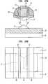
- FIG. 1shows a single crystal silicon unit cell, which is a cubic cell. Certain crystal directions, such as [001], [100], [010], [110], and [111], are specifically indicated by arrowheads in the cubic unit cell. Moreover, the crystal planes or facets of a single crystal silicon unit cell are defined by the notation (hkl) in Miller Index, which refers to a particular crystal plane or facet that is perpendicular to the [hkl] direction.
- FIG. 1shows a single crystal silicon unit cell, which is a cubic cell. Certain crystal directions, such as [001], [100], [010], [110], and [111], are specifically indicated by arrowheads in the cubic unit cell.
- the crystal planes or facets of a single crystal silicon unit cellare defined by the notation (hkl) in Miller Index, which refers to a particular crystal plane or facet that is perpendicular to the [hkl] direction.
- the ⁇ 100> directionsinclude the equivalent crystal directions of [100], [010], and [001];
- the ⁇ 110> directionsinclude the equivalent crystal directions of [110], [011], [101], [ ⁇ 1 ⁇ 10], [0 ⁇ 1 ⁇ 1], [ ⁇ 10 ⁇ 1], [ ⁇ 110], [0 ⁇ 11], [ ⁇ 101], [1 ⁇ 10], [01 ⁇ 1], and [10 ⁇ 1];
- the ⁇ 111> directionsinclude the equivalent crystal directions of [111], [ ⁇ 111], [1 ⁇ 11], and [11 ⁇ 1].
- the notation ⁇ hkl ⁇defines a family or set of equivalent crystal planes or facets that are respectively perpendicular to the ⁇ hkl> directions.
- the ⁇ 100 ⁇ planesinclude the set of equivalent crystal planes that are respectively perpendicular to the ⁇ 100> directions.
- Semiconductor waferstypically each has a substrate surface oriented along one of a single set of equivalent crystal planes of the single crystal semiconductor material (e.g., Si) that forms the wafers.
- the single crystal semiconductor materiale.g., Si
- most of today's semiconductor devicesare built upon silicon wafers having wafer surfaces oriented along one of the ⁇ 100 ⁇ crystal planes of silicon.
- electronsare known to have a high mobility along the ⁇ 100 ⁇ crystal planes of silicon
- holesare known to have high mobility along the ⁇ 110 ⁇ crystal planes of silicon.
- hole mobility values along the ⁇ 100 ⁇ planesare roughly about 2 to 4 times lower than the corresponding electron hole mobility values along such planes.
- hole mobility values along the ⁇ 110 ⁇ silicon surfacesare about 2 times higher than those along the ⁇ 100 ⁇ silicon surfaces, but electron mobility along the ⁇ 110 ⁇ surfaces are significantly degraded compared to those along the ⁇ 100 ⁇ surfaces.
- mechanical stresses within a semiconductor device substratecan also be used to modulate device performance.
- hole mobilityis enhanced when the silicon film is under compressive stress in the film direction and/or under tensile stress in a direction normal of the silicon film
- electron mobilityis enhanced when the silicon film is under tensile stress in the film direction and/or under compressive stress in the direction normal of the silicon film. Therefore, compressive and/or tensile stresses can be advantageously created in the channel regions of a p-FET and/or an n-FET in order to enhance the performance of such devices.
- the same stress componentdiscriminatively affects the performance of a p-FET and an n-FET.
- compressive stress in the source-drain direction and/or tensile stress in the direction normal of the gate dielectric layerenhances the performance of the p-FET, but adversely impacts the performance of the n-FET
- tensile stress in the source-drain direction and/or compressive stress in the direction normal of the gate dielectric layerenhances the performance of the n-FET, but adversely impacts the performance of the p-FET.
- p-FET and n-FETrequire different types of stresses for performance enhancement, which imposes a challenge for concurrent fabrication of high performance p-FET and n-FET, due to the difficulty in concurrently applying compressive stress in the source-drain direction to the p-FET and tensile stress to the n-FET, or concurrently applying tensile stress in the direction normal of the gate dielectric surface to the p-FET and compressive stress to the n-FET.
- Embedded SiGe stressorshave been used in the past to induce compressive strain in a p-FET channel region, consistent with the above-described approach.
- a compressively stressed silicon channel layercan be formed between embedded SiGe stressors that are epitaxially grown over a silicon substrate.
- the lattice constant of germaniumis greater than that of silicon, as shown in FIG. 3 .
- epitaxial growth of SiGe on a silicon substratewill yield SiGe stressor layers with compressive stress, and the compressively stressed SiGe stressors will in turn apply compressive stress to the channel region located therebetween.
- a tensilely stressed silicon channel layercan be formed between embedded Si:C stressors that are epitaxially grown over a silicon substrate. Because the lattice constant of carbon is smaller than that of silicon, as shown in FIG. 3 , epitaxial growth of Si:C over a silicon substrate will yield Si:C stressor layers with tensile stress, and the tensilely stressed Si:C stressors will in turn apply tensile stress to the channel region located therebetween.
- the embedded SiGe or Si:C stressorscan only be used to enhance the electron or hole mobility of one type of FETs (either n-type or p-type), but they will deleteriously reduce the carrier mobility in the complementary FETs.
- complementary Si:C or SiGe stressorscan be independently formed in the complementary FETs, the use of different stress-inducing materials for the p-FETs and the n-FETs requires additional processing steps, which will significantly increase the processing complexity as well as the manufacturing costs.
- stressor layers comprised of the same stress-inducing materialmay be used to induce different types of stress in a semiconductor device structure, by positioning or orienting such stressor layers differently.
- the present inventionrelates to a semiconductor device comprising a FET with a channel region located in a semiconductor device structure.
- the semiconductor device structurehas a top surface that is oriented along one of a first set of equivalent crystal planes and one or more additional surfaces that are oriented along a second, different set of equivalent crystal planes.
- One or more stressor layersare located over the one or more additional surfaces of the semiconductor device structure and are arranged and constructed to apply stress (either tensile or compressive) to the channel region of the FET.
- the semiconductor device structurecomprises single crystal silicon, and the first and second set of equivalent crystal planes are selected from the group consisting of the ⁇ 100 ⁇ , ⁇ 110 ⁇ , and ⁇ 111 ⁇ planes of silicon.
- the one or more stressor layerscomprise SiGe and contain intrinsic compressive stress due to lattice mismatch between SiGe and Si, which is contained by the semiconductor device structure.
- the one or more additional surfaces of the semiconductor device structureform acute angles with the top surface
- the one or more stressor layersapply tensile stress to the channel region of the FET.
- the one or more additional surfaces of the semiconductor device structureform obtuse angles with the top surface
- the one or more stressor layersapply compressive stress to the channel region of the FET.
- the one or more stressor layerscomprise Si:C and contain intrinsic tensile stress due to lattice mismatch between Si:C and Si, which is contained by the semiconductor device structure.
- the one or more stressor layersapply compressive stress to the channel region of the FET.
- the one or more additional surfaces of the semiconductor device structureform obtuse angles with the top surface, the one or more stressor layers apply tensile stress to the channel region of the FET.
- the semiconductor device structure of the present inventioncan be located over a substrate that comprises at least one insulator layer with a base semiconductor substrate layer thereunder, thereby forming a semiconductor-on-insulator (SOI) structure, or it can be located in a bulk semiconductor substrate structure. Further, the semiconductor device structure of the present invention may comprise a floating semiconductor body that is spaced apart from any substrate structure.
- SOIsemiconductor-on-insulator
- the present inventionrelates to a semiconductor device comprising an n-channel field effect transistor (n-FET) having an n-doped channel region located in a semiconductor device structure.
- the semiconductor device structurehas a top surface that is oriented along one of a first set of equivalent crystal planes and one or more additional surfaces that are oriented along a second, different set of equivalent crystal planes.
- One or more stressor layers with intrinsic compressive or tensile stressare located over said one or more additional surfaces of the semiconductor device structure and are arranged and constructed to apply tensile stress to the n-doped channel region of the n-FET.
- the one or more stressor layerscomprise SiGe with intrinsic compressive stress therein, and the one or more additional surfaces of the semiconductor device structure preferably form acute angles with the top surface, so that the stressor layers apply tensile stress to the channel region of the n-FET.
- the one or more stressor layerscomprise Si:C with intrinsic tensile stress therein, and the one or more additional surfaces of the semiconductor device structure form obtuse angles with the top surface, so that the one or more stressor layers apply tensile stress to the channel region of the n-FET.
- the present inventionrelates to a semiconductor device comprising a p-channel field effect transistor (p-FET) having a p-doped channel region located in a semiconductor device structure.
- the semiconductor device structurehas a top surface oriented along one of a first set of equivalent crystal planes and one or more additional surfaces oriented along a second, different set of equivalent crystal planes.
- One or more stressor layers with intrinsic compressive or tensile stressare located over the one or more additional surfaces of the semiconductor device structure and are arranged and constructed to apply compressive stress to the p-doped channel region of the p-FET.
- the one or more stressor layerscomprise SiGe with intrinsic compressive stress therein, and the one or more additional surfaces of the semiconductor device structure preferably form obtuse angles with the top surface, so that the stressor layers apply compressive stress to the channel region of the p-FET.
- the one or more stressor layerscomprise Si:C with intrinsic tensile stress therein, and the one or more additional surfaces of the semiconductor device structure form acute angles with the top surface, so that the one or more stressor layers apply compressive stress to the channel region of the p-FET.
- the present inventionrelates to a method for forming a semiconductor device, comprising:
- the semiconductor device structureis formed by:
- the one or more additional surfaces formed by the crystallographic etchingmay form either acute or obtuse angles with the top surface of the semiconductor device layer.
- the one or more stressor layercan be formed by epitaxially growing a semiconductor material having a lattice constant different from (i.e., either larger or smaller than) that of the semiconductor device structure, while the lattice mismatch between the stressor layers and the semiconductor device structure functions to generate corresponding stress in the stressor layers.
- FIG. 1shows a silicon crystal unit cell with certain crystal orientations specifically indicated by arrowheads.
- FIG. 2shows certain specific crystal planes in silicon crystal unit cells.
- FIG. 3illustrates crystal lattices of Si:C, Si, and SiGe and pseudomorphic growth of a second material layer having a smaller lattice constant (lattice 1) over a first material layer that has a larger lattice constant (lattice 2).
- FIG. 4is a simulated stress contour map that illustrates stress profiles around two SiGe structures embedded in a silicon substrate.
- FIG. 5is a cross-sectional view of an exemplary FET device with a channel region located in a trapezoidal semiconductor device structure with acute angles formed between a top surface and sidewall surfaces of the trapezoidal semiconductor device structure, according to one embodiment of the present invention.
- FIGS. 6-9illustrate exemplary processing steps that can be used for fabricating the FET device of FIG. 5 , according to one embodiment of the present invention.
- FIGS. 10-12illustrates exemplary processing steps that can be used for fabricating an exemplary FET device with a channel region located in a double trapezoid semiconductor device structure with acute angles formed between a top surface and sidewall surfaces of the double trapezoid semiconductor device structure, according to one embodiment of the present invention.
- FIG. 13is a cross-sectional view of an exemplary FET device with a channel region located in a trapezoidal semiconductor device structure with obtuse angles formed between a top surface and sidewall surfaces of the trapezoidal semiconductor device structure, according to one embodiment of the present invention.
- FIGS. 14-16illustrate exemplary processing steps that can be used for fabricating the FET device of FIG. 5 , according to one embodiment of the present invention.
- FIGS. 17-19illustrate exemplary processing steps that can be used for forming an exemplary FET device with a channel region located in a trapezoidal semiconductor device structure, which is similar to that shown by FIG. 13 but has significant undercut beneath the FET gate stack, according to one embodiment of the present invention.
- FIGS. 20-23illustrate exemplary processing steps for forming an FET device with a channel region located in an hourglass-shaped semiconductor device structure with acute angles formed between a top surface and sidewall surfaces of the hourglass-shaped semiconductor device structure, according to one embodiment of the present invention.
- FIGS. 24-26illustrate exemplary processing steps for forming an FET device with a channel region located in a semiconductor device structure that contains a floating semiconductor body with acute angles formed between a top surface and sidewall surfaces of the floating semiconductor body, according to one embodiment of the present invention.
- equivalent crystal planesrefers to a family of equivalent crystal planes or facets as defined by the Miller Indexes, as described hereinabove.
- Si:Cor “carbon-doped silicon” as used herein refers to a single crystal silicon having substitutional carbon atoms located therein.
- the substitutional carbon atoms and the silicon atomsform a silicon-carbon alloy, which is still a semiconductor material.
- the Si:C or carbon-doped silicon as used in the present inventionis therefore distinguished from silicon carbide, which is a dielectric material that contains a carbon-silicon compound.
- the present inventionprovides various configurations of semiconductor device structures with stressor layers that can be readily formed by crystallographic etching and pseudomorphic growth of semiconductor materials.
- the semiconductor device structures and the stressor layers of the present inventioncan be arranged and constructed in various different manners to provide different strain conditions in the channel regions of FET devices for achieving optimal device performance.
- the inventors of the present inventionhave discovered that a specific stress-inducing structure embedded in a semiconductor substrate can induce different types of stresses, depending on the locations of the stress measurement point in relation to the stress-inducing structure.
- FIG. 4shows the stress profile near two compressively stressed SiGe layers that are embedded in a silicon substrate.
- Two white dotted linesare drawn at the respective ends of the SiGe layers along directions that are perpendicular to the linear portions of such SiGe layers.
- Each compressively stressed SiGe layerinduces tensile stress in the region located at the side of the white dotted line that is immediately adjacent to the linear portion of the SiGe layer, but it induces compressive stress in the region located at the other side of the white dotted line away from the linear portion of the SiGe layer, as shown in FIG. 4 .
- a channel layeris formed in the silicon substrate of FIG. 4 within the region located at the side of the white dotted line that is immediately adjacent to the linear portion of the SiGe layer, such a channel layer will contain tensile stress and is therefore suitable for forming an n-channeled FET due to enhanced electron mobility.
- the channel layeris formed in the silicon substrate of FIG. 4 within the region located at the other side of the white dotted line away from the linear portion of the SiGe layer, such a channel layer will contain compressive stress and is suitable for forming a p-channeled FET instead, due to enhanced hole mobility.
- FIG. 4only shows the stress profile of compressively stressed SiGe layers that are embedded in a silicon substrate, a similar stress profile has been observed for tensilely stressed Si:C layers that are embedded in a silicon substrate, except that the types of stresses generated by the embedded Si:C layers are exactly opposite to those shown in FIG. 4 .
- the tensilely stressed Si:C layerswill induce compressive stress in the regions located at the sides of the white dotted lines that are immediately adjacent to the linear portions of the Si:C layers, but they will induce tensile stress in the regions located at the other sides of the white dotted lines away from the linear portions of the Si:C layers.
- embedded stressor layers containing a specific type of intrinsic stresscan be used to create different types of stresses in different regions of the semiconductor substrate, depending on the spatial relations of such regions with respect to the embedded stressor layers. Therefore, by changing the relative positions of FET channel regions with respect to the stressor layers, the same type of stressor layers can be used to create different types of stresses in the FET channels.
- the device performance of both n-FETs and p-FETscan be enhanced using the same type of stressor layers, with few or no additional processing steps.
- FIG. 5shows a cross-sectional view of an exemplary FET device with a channel region located in a trapezoidal semiconductor device structure 14 .
- the trapezoidal semiconductor device structure 14is located above a substrate structure that comprises an insulator layer 12 and a base semiconductor substrate 10 and underneath a gate stack that comprises a gate dielectric layer 22 , a gate conductor 24 , a dielectric cap layer 26 , and optional spacers 27 and 28 .
- the trapezoidal semiconductor device structure 14has an upper surface 14 A that is in direct contact with the gate dielectric layer 22 and two slanted sidewall surfaces 14 B. Acute angles are formed between the upper surface 14 A and the sidewall surfaces 14 B of the trapezoidal semiconductor device structure 14 .
- the FET channel(not shown) is defined by the gate stack and is therefore located in a portion of the trapezoidal semiconductor device structure 14 underneath the gate dielectric layer 22 .
- Two stressor layers 30which contain intrinsic stresses of either compressive or tensile type, are formed over the slanted sidewall surfaces 14 B of the trapezoidal semiconductor device structure 14 , as shown in FIG. 5 .
- Two dotted linescan be drawn at the respective ends of the stressor layers 30 along directions that are perpendicular to the linear portions of such stressor layers 30 .
- the stressor layers 30which contain a specific type of intrinsic stress (either compressive or tensile) will create an opposite type of stress in regions of the trapezoidal semiconductor device structure 14 that are located at the sides of the dotted lines immediately adjacent to the linear portions of the stressor layers 30 , and they will create the same type of stress in regions of the trapezoidal semiconductor device structure 14 that are located at the other sides of the dotted lines away from the linear portions of the stressor layers 30 .
- the FET channel(not shown), which is located in the portion of the trapezoidal semiconductor structure 14 directly underneath the gate dielectric layer 22 , will have an opposite type of stress in comparison with the intrinsic stress contained by the stressor layers 30 .
- the stressor layers 30contain intrinsic compressive stress
- the FET channel (not shown)will have tensile stress and is thus suitable for forming an n-channel in an n-FET due to enhanced electron mobility.
- the stressor layers 30contain intrinsic tensile stress
- the FET channel (not shown)will have compressive stress created therein and is then suitable for forming a p-channel in a p-FET due to enhanced hole mobility.
- FIGS. 6-9illustrate exemplary processing steps that can be used for fabricating the FET device of FIG. 5 , according to one embodiment of the present invention.
- a patterned gate stackwhich comprises a gate dielectric layer 22 , a gate conductor layer 24 , a dielectric cap layer 26 , and optional spacers 27 and 28 , is formed over a substrate structure 5 , which preferably has a semiconductor-on-insulator (SOI) configuration and comprises a base semiconductor substrate 10 , an insulator layer 12 , and a semiconductor device layer 13 , as shown in FIG. 6 .
- SOIsemiconductor-on-insulator
- the base semiconductor substrate 10may comprise any suitable semiconductor material, which includes, but is not limited to: Si, SiC, SiGe, SiGeC, Ge alloys, GaAs, InAs, InP, as well as other III-V or II-VI compound semiconductors, either in their single crystalline or polycrystalline form.
- the base semiconductor substrate 10may also comprise an organic semiconductor or a layered semiconductor such as Si/SiGe, a silicon-on-insulator (SOI) or a SiGe-on-insulator (SGOI).
- the base semiconductor substrate 10is composed of a Si-containing semiconductor material, i.e., a semiconductor material that includes silicon. More preferably, the base semiconductor substrate 10 consists essentially of bulk single crystal silicon.
- the base semiconductor substrate 10may comprise one or more buried insulator layers (not shown) therein.
- the base semiconductor substrate layer 10may be doped, undoped or contain both doped and undoped regions (not shown) therein.
- the insulator layer 12may comprise any suitable insulator material(s), and it typically comprises an oxide, a nitride, or an oxynitride in either a crystalline phase or a non-crystalline phase.
- the physical thickness of the insulator layer 12typically ranges from about 10 nm to about 400 nm, and more typically from about 20 nm to about 200 nm.
- the semiconductor device layer 13may comprise any single crystal semiconductor material, which includes, but is not limited to: Si, SiC, SiGe, SiGeC, Ge alloys, GaAs, InAs, InP, as well as other III-V or II-VI compound semiconductors.
- the semiconductor device layer 13is composed of a Si-containing semiconductor material, i.e., a semiconductor material that includes silicon. More preferably, the semiconductor device layer 13 consists essentially of single crystal silicon and has an upper surface 13 A that is oriented along one of a first set of equivalent crystal planes of silicon.
- the upper surface 13 A of the semiconductor device layer 13is oriented along one of the ⁇ 100 ⁇ planes of silicon, so that the semiconductor device layer 13 can be used for forming a channel region for an n-FET device.
- the upper surface 13 A of the semiconductor device layer 13is oriented along one of the ⁇ 110 ⁇ planes of silicon, so that the semiconductor device layer 13 can be used for forming a channel region for a p-FET device.
- the semiconductor device layer 13 and the base semiconductor substrate layer 10may be formed of the same semiconductor material or different types of semiconductor materials.
- the SOI substrate structure 5 as shown in FIG. 6can be formed in situ by depositing the insulator layer 12 over the base semiconductor substrate layer 10 via chemical vapor deposition, thermal oxidation or a combination thereof, followed by deposition of the semiconductor device layer 13 .
- the SOI substrate structure 5 of FIG. 6can be formed in situ by a silicon implanted oxide (SIMOX) process, during which oxygen ions are implanted into a bulk semiconductor substrate at a predetermined depth, followed by high temperature anneal to effectuate reaction between the semiconductor material and the implanted oxygen ions, thereby forming an oxide layer in the semiconductor substrate at the predetermined depth.
- SIMOXsilicon implanted oxide
- the SOI substrate structure 5 of FIG. 6may be fabricated from pre-formed insulator and semiconductor layers by wafer-bonding or layer transfer techniques.
- the gate dielectric layer 22 of the present inventionmay be comprised of any suitable dielectric material, including, but not limited to: oxides, nitrides, oxynitrides and/or silicates (including metal silicates and nitrided metal silicates).
- the gate dielectric layer 22is comprised of an oxide such as, for example, SiO 2 , HfO 2 , ZrO 2 , Al 2 O 3 , TiO 2 , La 2 O 3 , SrTiO 3 , LaAlO 3 , and mixtures thereof.
- the physical thickness of the gate dielectric layer 22may vary widely, depending on the specific deposition technique employed.
- the gate dielectric layer 24has a thickness from about 0.5 to about 10 nm, with a thickness from about 1 to about 5 nm being more typical.
- the gate dielectric layer 22can be formed by a thermal growing process such as, for example, oxidation, nitridation or oxynitridation.
- the gate dielectric layer 22can be formed by a deposition process such as, for example, chemical vapor deposition (CVD), plasma-assisted CVD, atomic layer deposition (ALD), evaporation, reactive sputtering, chemical solution deposition and other like deposition processes.
- CVDchemical vapor deposition
- ALDatomic layer deposition
- evaporationreactive sputtering
- chemical solution depositionchemical solution deposition and other like deposition processes.
- the gate dielectric layer 22may also be formed utilizing any combination of the above processes.
- the gate conductor 24 and the optional dielectric cap layer 26are formed over the gate dielectric layer 22 , by first depositing a blanket gate conductor layer (not shown) and a blanket dielectric capping layer (not shown) over the gate dielectric layer 22 , followed by patterning the blanket gate conductor layer (not shown) and the dielectric capping layer (not shown) into the gate conductor 24 and the optional dielectric cap layer 26 using conventional lithography and etching.
- the lithography steppreferably inverse gate level (PC) lithography, includes applying a photoresist (not shown) to the upper surface of the blanket dielectric capping layer (not shown), exposing the photoresist (not shown) to a desired pattern of radiation and developing the exposed photoresist (not shown) utilizing a conventional resist developer.
- the pattern in the photoresist (not shown)is then transferred to the underneath dielectric capping layer (not shown), the blanket gate conductor layer (not shown), and the blanket gate dielectric layer (not shown) utilizing one or more dry etching steps.
- Suitable dry etching processesthat can be used in the present invention include, but are not limited to: reactive ion etching (RIE), ion beam etching, plasma etching or laser ablation.
- RIEreactive ion etching
- the gate conductor layer 24comprises polycrystalline silicon (poly-Si)
- the dielectric capping layer 26comprises silicon nitride.
- the etching steppreferably is carried out by RIE techniques.
- the patterned photoresist(not shown) is then removed by resist stripping after etching has been completed.
- FIG. 6shows formation of the gate stack before subsequent processing steps, such as etching, stressor deposition, and dopant implantation
- a dummy gate(not shown) can be first formed in place of the gate stack as shown hereinabove in FIG. 6 , and such a dummy gate (not shown) can then be replaced by a functional gate stack during a replacement gate process after the subsequent processing steps have been completed.
- an anisotropic etching stepis carried out using the gate stack as a mask to pattern the semiconductor device layer 13 , as shown in FIG. 7 .
- the patterned semiconductor device layer 13contains exposed sidewalls 13 B that are aligned with the gate stack, and such exposed sidewalls 13 B are oriented along the same set of equivalent crystal planes as the upper surface 13 A of the semiconductor device layer 13 .
- Any suitable etching chemistrythat selectively etches silicon over silicon oxide and silicon nitride in an anisotropic manner can be used for patterning the semiconductor layer 13 .
- the anisotropic etching of the semiconductor device layer 13is carried out by using one or more dry-etching processes, such as reactive ion etching (RIE), sputter etching, vapor phase etching, ion beam etching, plasma etching, and laser ablation.
- RIEreactive ion etching
- the dry-etching processesare directional (i.e., anisotropic), but they are mostly non-selective to different crystal planes or orientations, i.e., they etch the semiconductor material in approximately equal rates along all directions.
- the semiconductor device layer 13is patterned using a reactive ion etching (RIE) process.
- RIEreactive ion etching
- a lateral etching stepis subsequently carried out to selectively removing a potion of the insulator layer 12 from underneath the patterned semiconductor layer 13 , thereby forming undercut regions 2 and exposing portions of a lower surface 13 C of the patterned semiconductor device layer 13 , as shown in FIG. 8 .
- the lateral etching stepcan be carried out using any suitable etching chemistry that selectively etches the insulator material contained by layer 12 over the semiconductor material contained by the semiconductor device layer 13 .
- a crystallographic etching stepis carried out to etch the exposed sidewall surfaces 13 B and the exposed portions of the lower surface 13 C of the patterned semiconductor device layer 13 .
- Crystallographic etching of the semiconductor device layer 13is preferably carried out by one or more wet-etching processes, which employ etching solutions such as hydroxide-based etching solutions, ethylene diamine pyrocatechol (EDP)-based etching solutions, etc., to etch the semiconductor device layer 13 at significantly different rates along different crystal planes or orientations. Therefore, the crystallographic etching is an isotropic process, but the etching pattern formed by the crystallographic etching process proceeds along the fast-etched crystal planes and is eventually terminated by the slowly etched crystal planes.
- etching solutionssuch as hydroxide-based etching solutions, ethylene diamine pyrocatechol (EDP)-based etching solutions, etc.
- an etching solutionthat comprises approximately 23.4% KOH, 13.3% isopropyl alcohol (IPA), and 63.3% water, when heated to about 80° C., etches the single crystal silicon at an etching rate of about 1.0 ⁇ m/minute along the ⁇ 100 ⁇ planes, but at an etching rate of about 0.06 ⁇ m/minute along the ⁇ 110 ⁇ planes.
- this etching solutionetches the ⁇ 100 ⁇ planes about 17 times faster than the ⁇ 110 ⁇ planes. Therefore, such an etching solution can be used to etch a silicon substrate to form a recess that is terminated at the ⁇ 110 ⁇ planes.
- an etching solutionthat comprises approximately 44% KOH and 56% water, when heated to about 120° C., etches the single crystal silicon at an etching rate of about 11.7 ⁇ m/minute along the ⁇ 110 ⁇ planes, about 5.8 ⁇ m/minute along the ⁇ 100 ⁇ planes, and about 0.02 ⁇ m/minute along the ⁇ 111 ⁇ planes.
- this etching solutionetches the ⁇ 110 ⁇ and ⁇ 100 ⁇ planes significantly faster than the ⁇ 111 ⁇ planes (more than 550 and 250 times faster, respectively). Therefore, such an etching solution can be used to etch a silicon substrate to form a recess that is terminated at the ⁇ 111 ⁇ planes.
- the crystallographic etching stepis carried out using an etching chemistry that etches the crystal planes of the exposed lower surface 13 C and the sidewall surfaces 13 B of the semiconductor device layer 13 at an etching rate faster than other crystal planes, so that the crystallographic etching terminates along a set of crystal planes that is different from the lower surface 13 C and the sidewall surfaces 13 B.
- the semiconductor device layer 13is crystallographically etched to form a trapezoidal semiconductor device structure 14 with an upper surface 14 A oriented along a first set of crystal planes and sidewall surfaces 14 B oriented along a second, different set of crystal planes.
- the second, different set of crystal planesare slanted away from the first set of crystal planes, and acute angles are formed between the upper surface 14 A and the sidewall surfaces 14 B of the trapezoidal semiconductor device structure 14 .
- RIEreactive ion etching
- the substrateis placed inside a reactor in which several gases are introduced.
- a plasmais introduced in the gas mixture using an radio-frequency (RF) power source, breaking the gas molecules into ions.
- the ionsare accelerated towards, and react at, the surface of the material being etched, forming another gaseous material. This is known as the chemical part of reactive ion etching, which is isotropic.
- the RIEalso has a physical aspect: if the ions have high enough energy, the ions can knock atoms out of the material to be etched without a chemical reaction.
- RIEis a complex process that involves both chemical and physical etching. By carefully adjusting the balance between the chemicals aspect and the physical aspect of RIE, this process can be used to achieve either anisotropic or crystallographic etching results.
- wet-etchingis typically used for the crystallographic etching, certain wet-etching chemistries can also be used to achieve anisotropic etching results.
- the present inventionis not limited to the use of dry-etching for the anisotropic etching process and the use of wet-etching for the crystallographic etching process, but encompasses all suitable etching processes and techniques that can be used to achieved the desired anisotropic and crystallographic results as described hereinabove.
- an epitaxial growth stepcan be carried out to pseudomorphically grow the stressor structures 30 along the slanted sidewalls 14 B of the trapezoidal semiconductor device structure 14 so as to form the FET device structure in FIG. 5 .
- the stressor structures 30may comprise any semiconductor material having a lattice constant different from that of the trapezoidal semiconductor device structure 14 , so that lattice mismatch between the stressor structures 30 and the semiconductor device structure 14 can generate tensile or compressive stress in the stressor structures 30 as well as in the semiconductor device structure 14 , as described hereinabove.
- the stressor structures 30contain SiGe
- compressive stresswill be created in the stressor structures 30
- tensile stresswill be created in the FET channel (not shown) located in the trapezoidal semiconductor device structure 14 .
- the trapezoidal semiconductor device structure 14is suitable for forming an n-channel in an n-FET.
- the trapezoidal semiconductor device structure 14is suitable for forming an p-channel in a p-FET.
- CMOS processing stepssuch as source/drain extension implantation, source/drain implantation, salicidation, etc., can be further carried out to form a complete FET (either n-channel or p-channel) device structure, which contain a channel region with the desired stress (either tensile or compressive).
- FIGS. 10-12illustrates exemplary processing steps that can be used for fabricating an exemplary FET device with a channel region located in a double trapezoid semiconductor device structure with acute angles formed between a top surface and sidewall surfaces of the double trapezoid semiconductor device structure, according to one embodiment of the present invention.
- a lateral etching stepis carried out to form relatively small undercut regions 2 (in comparison with those shown in FIG. 8 ), so that the subsequent crystallographic etching of the semiconductor device layer 13 forms a double trapezoid semiconductor device structure 14 with an upper surface 14 A and sidewall surfaces 14 B, as shown in FIGS. 10-11 .
- Upper portions of the sidewall surfaces 14 Bstill form acute angles with the upper surface 14 A of the double trapezoid semiconductor device structure 14 , as shown in FIG. 11 , although lower portions of the sidewall surfaces 14 B now flare out to form a base for the double trapezoid semiconductor device structure 14 .
- An epitaxial growth stepcan then be carried out to pseudomorphically grow stressor structures 30 along both the upper and lower portions of the sidewalls 14 B of the double trapezoidal semiconductor device structure 14 , as shown in FIG. 12 .
- FIG. 13is a cross-sectional view of an exemplary FET device with a channel region located in a trapezoidal semiconductor device structure 15 , according to one embodiment of the present invention.
- the trapezoidal semiconductor device structure 15 of FIG. 13is similar to the trapezoidal semiconductor device structure 14 of FIG. 5 , except that obtuse (instead of acute) angles are formed between a top surface 15 A and sidewall surfaces 15 B of the trapezoidal semiconductor device structure 15 .
- the stressor layers 30are formed over the slanted sidewall surfaces 14 B of the trapezoidal semiconductor device structure 15 , as shown in FIG. 13 .
- Two dotted linescan be drawn at the respective ends of the stressor layers 30 along directions that are perpendicular to the linear portions of such stressor layers 30 .
- the stressor layers 30which contain a specific type of intrinsic stress (either compressive or tensile) will create an opposite type of stress in regions of the trapezoidal semiconductor device structure 15 that are located at the sides of the dotted lines immediately adjacent to the linear portions of the stressor layers 30 , and they will create the same type of stress in regions of the trapezoidal semiconductor device structure 15 that are located at the other sides of the dotted lines away from the linear portions of the stressor layers 30 .
- the FET channel(not shown), which is located in the portion of the trapezoidal semiconductor structure 15 directly underneath the gate dielectric layer 22 , will have the same type of stress as that contained by the stressor layers 30 .
- the stressor layers 30contain intrinsic compressive stress
- the FET channel (not shown)will have compressive stress and is thus suitable for forming a p-channel in a p-FET due to enhanced hole mobility.
- the stressor layers 30contain intrinsic tensile stress
- the FET channel (not shown)will have tensile stress created therein and is then suitable for forming an n-channel in an n-FET due to enhanced electron mobility.
- the trapezoidal semiconductor device structure 15 of FIG. 13can be readily formed by exemplary processing steps of FIGS. 14-16 , according to one embodiment of the present invention.
- a patterned gate stackwhich comprises a gate dielectric layer 22 , a gate conductor layer 24 , a dielectric cap layer 26 , and optional spacers 27 and 28 , is formed over a substrate structure 5 , which preferably has a semiconductor-on-insulator (SOI) configuration and comprises a base semiconductor substrate 10 , an insulator layer 12 , and a semiconductor device layer 13 , as shown in FIG. 14 .
- SOIsemiconductor-on-insulator
- an anisotropic etching stepis carried out to pattern the semiconductor device layer 13 , while a portion of the upper surface 13 A and the sidewall surfaces 13 B of the device layer 13 are exposed, as shown in FIG. 15 .
- FIGS. 17-19illustrate exemplary processing steps that can be used for forming another exemplary FET device with a channel region located in a trapezoidal semiconductor device structure, which is similar to that shown by FIG. 13 but has significant undercut beneath the FET gate stack, according to one embodiment of the present invention.
- the semiconductor device layer 13is patterned by an anisotropic etching step, while a relatively smaller portion (in comparison with that shown in FIG. 15 ) of the upper surface 13 A of the layer 13 is exposed, as shown in FIG. 17 .
- Subsequent crystallographic etching of such a patterned semiconductor device layer 13thus forms a trapezoidal semiconductor device structure 15 that undercuts the gate stack, as shown in FIG. 18 .
- Pseudomorphic growth of stressor structures 30 over the sidewall surfaces 15 B of the trapezoidal semiconductor device structure 15 of FIG. 18will form the FET device as shown in FIG. 19 .
- FIGS. 20-23illustrate exemplary processing steps for forming an FET device with a channel region located in an hourglass-shaped semiconductor device structure, according to one embodiment of the present invention.
- a patterned gate stackwhich comprises a gate dielectric layer 22 , a gate conductor layer 24 , a dielectric cap layer 26 , and optional spacers 27 and 28 , is first formed over a bulk semiconductor substrate structure 13 that has an upper surface 13 A, as shown in FIG. 20 .
- An anisotropic etching stepis then carried out to form trenches 11 with exposed trench sidewalls 13 B in the bulk semiconductor substrate structure 13 , as shown in FIG. 21 .
- FIGS. 24-26illustrate exemplary processing steps for forming an FET device with a channel region located in a semiconductor device structure that contains a floating semiconductor body, according to one embodiment of the present invention.
- a patterned gate stackwhich comprises a gate dielectric layer 22 , a gate conductor layer 24 , a dielectric cap layer 26 , and optional spacers 27 and 28 , is formed over a substrate structure 5 , which preferably has a semiconductor-on-insulator (SOI) configuration and comprises a base semiconductor substrate 10 , an insulator layer 12 , and a semiconductor device layer 13 .
- the semiconductor device layer 13has an upper surface 13 A, and an anisotropic etching step is carried out to form trenches 11 with exposed trench sidewalls 13 B in the bulk semiconductor substrate structure 13 , as shown in FIG. 24A .
- FIG. 24Bshows a top view of the structure shown by FIG. 24A .
- the patterned gate stackextends beyond the active region defined by the semiconductor device layer 13 to the adjacent isolation regions 9 .
- the adjacent isolation regions 9provide the necessary structural support for the gate stack, so that the semiconductor device layer 13 can be crystallographically etched to form a semiconductor device structure 17 that comprises a floating upper portion directly underneath the gate stack and a lower portion that is located over the insulator layer 12 but is disconnected from the floating upper portion, as shown in FIG. 25A .
- the floating upper portion of the semiconductor device structure 17has an upper surface 17 A and sidewall surfaces 17 B, while acute angles are formed between the upper surface 17 A and the sidewall surfaces 17 B.
- FIG. 25Bshows a top view of the structure of FIG. 24A .
- the floating upper portion of the semiconductor device structure 17is visible through the gate stack in FIG. 25B .
- Pseudomorphic growth of stressor structures 30 over the sidewall surfaces 17 B of the semiconductor device structure 17 of FIG. 25Awill form the FET device as shown in FIG. 26 .
- FIGS. 5-26illustratively demonstrate exemplary CMOS device structures and processing steps according to specific embodiments of the present invention
- CMOS device structures and processing stepsfor adaptation to specific application requirements, consistent with the above descriptions.
- the semiconductor substrates shown in FIGS. 5-26illustrate semiconductor substrates with upper surfaces oriented along the ⁇ 110 ⁇ or ⁇ 100 ⁇ crystal planes of single crystal silicon
- other suitable crystal planessuch as the ⁇ 111 ⁇ , ⁇ 211 ⁇ , ⁇ 311 ⁇ , ⁇ 511 ⁇ , and ⁇ 711 ⁇ planes of single crystal silicon, can also be used in the semiconductor substrates of the present invention.
- CMOS devicescan also be used for fabricating the CMOS devices of the present invention.
- a person ordinarily skilled in the artcan readily modify the device structures and processing steps illustrated in FIGS. 5-26 for adaptation to other substrate structures, crystal orientations, or semiconductor materials, consistent with the spirit and principles of the present invention.
Landscapes
- Engineering & Computer Science (AREA)
- General Physics & Mathematics (AREA)
- Physics & Mathematics (AREA)
- Condensed Matter Physics & Semiconductors (AREA)
- Manufacturing & Machinery (AREA)
- Computer Hardware Design (AREA)
- Microelectronics & Electronic Packaging (AREA)
- Power Engineering (AREA)
- General Chemical & Material Sciences (AREA)
- Chemical Kinetics & Catalysis (AREA)
- Chemical & Material Sciences (AREA)
- Insulated Gate Type Field-Effect Transistor (AREA)
- Metal-Oxide And Bipolar Metal-Oxide Semiconductor Integrated Circuits (AREA)
- Thin Film Transistor (AREA)
Abstract
Description
- forming a semiconductor device structure having a top surface that is oriented along one of a first set of equivalent crystal planes and one or more additional surfaces that are oriented along a second, different set of equivalent crystal planes;
- forming one or more stressor layers with intrinsic compressive or tensile stress over the one or more additional surfaces of the semiconductor device structure, wherein the one or more stressor layers are arranged and constructed to apply tensile or compressive stress to the semiconductor device structure; and
- forming an field effect transistor (FET) with a channel region located in the semiconductor device structure.
- forming a semiconductor device layer having at least a top surface oriented along one of a first set of equivalent crystallographic planes;
- selectively covering a portion of the semiconductor device layer;
- anisotropically etching an uncovered portion of the semiconductor device layer to expose at least one of a bottom surface and one or more sidewall surfaces of the semiconductor device layer, the bottom surface and the sidewall surfaces are oriented along the first set of equivalent crystallographic planes; and
- crystallographically etching the at least one of the bottom surface and sidewall surfaces of the semiconductor device layer to form one or more additional surfaces that are oriented along a second, different set of equivalent crystallographic planes.
Claims (10)
Priority Applications (8)
| Application Number | Priority Date | Filing Date | Title |
|---|---|---|---|
| US11/427,495US8853746B2 (en) | 2006-06-29 | 2006-06-29 | CMOS devices with stressed channel regions, and methods for fabricating the same |
| CN200780010670XACN101410968B (en) | 2006-06-29 | 2007-05-22 | Improved CMOS device with stressed channel region and method of manufacturing same |
| PCT/EP2007/054932WO2008000556A1 (en) | 2006-06-29 | 2007-05-22 | Improved cmos devices with stressed channel regions, and methods for fabricating the same |
| JP2009517065AJP5443983B2 (en) | 2006-06-29 | 2007-05-22 | Improved CMOS device having a stressed channel region and method of manufacturing the same (semiconductor device and method of forming the semiconductor device) |
| EP07729372AEP2041785A1 (en) | 2006-06-29 | 2007-05-22 | Improved cmos devices with stressed channel regions, and methods for fabricating the same |
| KR1020087030918AKR20090023615A (en) | 2006-06-29 | 2007-05-22 | Improved CMOS device with stressed channel region and method of manufacturing the same |
| TW096121843ATW200822361A (en) | 2006-06-29 | 2007-06-15 | Improved CMOS devices with stressed channel regions, and methods for fabricating the same |
| US14/507,242US20150162446A1 (en) | 2006-06-29 | 2014-10-06 | Cmos devices with stressed channel regions, and methods for fabricating the same |
Applications Claiming Priority (1)
| Application Number | Priority Date | Filing Date | Title |
|---|---|---|---|
| US11/427,495US8853746B2 (en) | 2006-06-29 | 2006-06-29 | CMOS devices with stressed channel regions, and methods for fabricating the same |
Related Child Applications (1)
| Application Number | Title | Priority Date | Filing Date |
|---|---|---|---|
| US14/507,242DivisionUS20150162446A1 (en) | 2006-06-29 | 2014-10-06 | Cmos devices with stressed channel regions, and methods for fabricating the same |
Publications (2)
| Publication Number | Publication Date |
|---|---|
| US20080001182A1 US20080001182A1 (en) | 2008-01-03 |
| US8853746B2true US8853746B2 (en) | 2014-10-07 |
Family
ID=38370438
Family Applications (2)
| Application Number | Title | Priority Date | Filing Date |
|---|---|---|---|
| US11/427,495Active2029-03-25US8853746B2 (en) | 2006-06-29 | 2006-06-29 | CMOS devices with stressed channel regions, and methods for fabricating the same |
| US14/507,242AbandonedUS20150162446A1 (en) | 2006-06-29 | 2014-10-06 | Cmos devices with stressed channel regions, and methods for fabricating the same |
Family Applications After (1)
| Application Number | Title | Priority Date | Filing Date |
|---|---|---|---|
| US14/507,242AbandonedUS20150162446A1 (en) | 2006-06-29 | 2014-10-06 | Cmos devices with stressed channel regions, and methods for fabricating the same |
Country Status (7)
| Country | Link |
|---|---|
| US (2) | US8853746B2 (en) |
| EP (1) | EP2041785A1 (en) |
| JP (1) | JP5443983B2 (en) |
| KR (1) | KR20090023615A (en) |
| CN (1) | CN101410968B (en) |
| TW (1) | TW200822361A (en) |
| WO (1) | WO2008000556A1 (en) |
Cited By (2)
| Publication number | Priority date | Publication date | Assignee | Title |
|---|---|---|---|---|
| US9390982B2 (en)* | 2013-09-13 | 2016-07-12 | Taiwan Semiconductor Manufacturing Company, Ltd. | CMOS devices with reduced leakage and methods of forming the same |
| US20180226347A1 (en)* | 2017-02-08 | 2018-08-09 | Globalfoundries Inc. | Heterojunction Bipolar Transistors With Stress Material For Improved Mobility |
Families Citing this family (25)
| Publication number | Priority date | Publication date | Assignee | Title |
|---|---|---|---|---|
| US7504301B2 (en)* | 2006-09-28 | 2009-03-17 | Advanced Micro Devices, Inc. | Stressed field effect transistor and methods for its fabrication |
| US7691752B2 (en)* | 2007-03-30 | 2010-04-06 | Intel Corporation | Methods of forming improved EPI fill on narrow isolation bounded source/drain regions and structures formed thereby |
| DE102007015504B4 (en)* | 2007-03-30 | 2014-10-23 | Advanced Micro Devices, Inc. | SOI transistor having reduced length drain and source regions and a strained dielectric material adjacent thereto and method of fabrication |
| FR2914783A1 (en)* | 2007-04-03 | 2008-10-10 | St Microelectronics Sa | METHOD FOR MANUFACTURING CONCENTRATING GRADIENT DEVICE AND CORRESPONDING DEVICE. |
| JP2010067930A (en)* | 2008-09-12 | 2010-03-25 | Toshiba Corp | Semiconductor device and method of manufacturing the same |
| US7994014B2 (en)* | 2008-10-10 | 2011-08-09 | Advanced Micro Devices, Inc. | Semiconductor devices having faceted silicide contacts, and related fabrication methods |
| US8455859B2 (en) | 2009-10-01 | 2013-06-04 | Taiwan Semiconductor Manufacturing Company, Ltd. | Strained structure of semiconductor device |
| US8035141B2 (en)* | 2009-10-28 | 2011-10-11 | International Business Machines Corporation | Bi-layer nFET embedded stressor element and integration to enhance drive current |
| US8338258B2 (en) | 2009-11-25 | 2012-12-25 | International Business Machines Corporation | Embedded stressor for semiconductor structures |
| US8765556B2 (en)* | 2009-12-23 | 2014-07-01 | Taiwan Semiconductor Manufacturing Company, Ltd. | Method of fabricating strained structure in semiconductor device |
| US8236660B2 (en) | 2010-04-21 | 2012-08-07 | International Business Machines Corporation | Monolayer dopant embedded stressor for advanced CMOS |
| US8299535B2 (en) | 2010-06-25 | 2012-10-30 | International Business Machines Corporation | Delta monolayer dopants epitaxy for embedded source/drain silicide |
| DE102010046215B4 (en)* | 2010-09-21 | 2019-01-03 | Infineon Technologies Austria Ag | Semiconductor body with strained region, electronic component and a method for producing the semiconductor body. |
| US8524614B2 (en)* | 2010-11-29 | 2013-09-03 | International Business Machines Corporation | III-V compound semiconductor material passivation with crystalline interlayer |
| US8372705B2 (en) | 2011-01-25 | 2013-02-12 | International Business Machines Corporation | Fabrication of CMOS transistors having differentially stressed spacers |
| CN102842493A (en)* | 2011-06-20 | 2012-12-26 | 中国科学院微电子研究所 | Semiconductor structure and manufacturing method thereof |
| US9142642B2 (en)* | 2012-02-10 | 2015-09-22 | Taiwan Semiconductor Manufacturing Company, Ltd. | Methods and apparatus for doped SiGe source/drain stressor deposition |
| KR101909204B1 (en)* | 2012-06-25 | 2018-10-17 | 삼성전자 주식회사 | Semiconductor device having embedded strain-inducing pattern and method of forming the same |
| US9356092B2 (en)* | 2013-09-12 | 2016-05-31 | Infineon Technologies Ag | Semiconductor device and method for manufacturing a semiconductor device |
| KR102152285B1 (en)* | 2014-12-08 | 2020-09-04 | 삼성전자주식회사 | Semiconductor device having stressor and method of forming the same |
| US9865520B2 (en)* | 2015-08-07 | 2018-01-09 | International Business Machines Corporation | Tunable semiconductor band gap reduction by strained sidewall passivation |
| KR102608191B1 (en) | 2016-08-09 | 2023-12-01 | 에스케이하이닉스 주식회사 | Semiconductor device and method of manufacturing the same |
| US10263077B1 (en)* | 2017-12-22 | 2019-04-16 | Commissariat A L'energie Atomique Et Aux Energies Alternatives | Method of fabricating a FET transistor having a strained channel |
| WO2020130599A1 (en)* | 2018-12-18 | 2020-06-25 | ㈜아모레퍼시픽 | Electronic device attachable to skin and manufacturing method therefor |
| US11109796B2 (en) | 2018-12-18 | 2021-09-07 | Amorepacific Corporation | Electronic device which can be adhered to skin and method for manufacturing the same |
Citations (99)
| Publication number | Priority date | Publication date | Assignee | Title |
|---|---|---|---|---|
| US3602841A (en) | 1970-06-18 | 1971-08-31 | Ibm | High frequency bulk semiconductor amplifiers and oscillators |
| US4665415A (en) | 1985-04-24 | 1987-05-12 | International Business Machines Corporation | Semiconductor device with hole conduction via strained lattice |
| JPS6476755A (en) | 1987-09-18 | 1989-03-22 | Hitachi Ltd | Semiconductor device |
| US4853076A (en) | 1983-12-29 | 1989-08-01 | Massachusetts Institute Of Technology | Semiconductor thin films |
| US4855245A (en) | 1985-09-13 | 1989-08-08 | Siemens Aktiengesellschaft | Method of manufacturing integrated circuit containing bipolar and complementary MOS transistors on a common substrate |
| US4952524A (en) | 1989-05-05 | 1990-08-28 | At&T Bell Laboratories | Semiconductor device manufacture including trench formation |
| US4958213A (en) | 1987-12-07 | 1990-09-18 | Texas Instruments Incorporated | Method for forming a transistor base region under thick oxide |
| US5006913A (en) | 1988-11-05 | 1991-04-09 | Mitsubishi Denki Kabushiki Kaisha | Stacked type semiconductor device |
| US5060030A (en) | 1990-07-18 | 1991-10-22 | Raytheon Company | Pseudomorphic HEMT having strained compensation layer |
| US5081513A (en) | 1991-02-28 | 1992-01-14 | Xerox Corporation | Electronic device with recovery layer proximate to active layer |
| US5108843A (en) | 1988-11-30 | 1992-04-28 | Ricoh Company, Ltd. | Thin film semiconductor and process for producing the same |
| US5134085A (en) | 1991-11-21 | 1992-07-28 | Micron Technology, Inc. | Reduced-mask, split-polysilicon CMOS process, incorporating stacked-capacitor cells, for fabricating multi-megabit dynamic random access memories |
| JPH065483B2 (en) | 1987-04-23 | 1994-01-19 | 大阪機工株式会社 | Automatic mold processing equipment |
| US5310446A (en) | 1990-01-10 | 1994-05-10 | Ricoh Company, Ltd. | Method for producing semiconductor film |
| US5354695A (en) | 1992-04-08 | 1994-10-11 | Leedy Glenn J | Membrane dielectric isolation IC fabrication |
| US5371399A (en) | 1991-06-14 | 1994-12-06 | International Business Machines Corporation | Compound semiconductor having metallic inclusions and devices fabricated therefrom |
| US5391510A (en) | 1992-02-28 | 1995-02-21 | International Business Machines Corporation | Formation of self-aligned metal gate FETs using a benignant removable gate material during high temperature steps |
| US5459346A (en) | 1988-06-28 | 1995-10-17 | Ricoh Co., Ltd. | Semiconductor substrate with electrical contact in groove |
| US5557122A (en) | 1995-05-12 | 1996-09-17 | Alliance Semiconductors Corporation | Semiconductor electrode having improved grain structure and oxide growth properties |
| US5561302A (en) | 1994-09-26 | 1996-10-01 | Motorola, Inc. | Enhanced mobility MOSFET device and method |
| US5670798A (en) | 1995-03-29 | 1997-09-23 | North Carolina State University | Integrated heterostructures of Group III-V nitride semiconductor materials including epitaxial ohmic contact non-nitride buffer layer and methods of fabricating same |
| US5679965A (en) | 1995-03-29 | 1997-10-21 | North Carolina State University | Integrated heterostructures of Group III-V nitride semiconductor materials including epitaxial ohmic contact, non-nitride buffer layer and methods of fabricating same |
| US5861651A (en) | 1997-02-28 | 1999-01-19 | Lucent Technologies Inc. | Field effect devices and capacitors with improved thin film dielectrics and method for making same |
| US5880040A (en) | 1996-04-15 | 1999-03-09 | Macronix International Co., Ltd. | Gate dielectric based on oxynitride grown in N2 O and annealed in NO |
| US5940736A (en) | 1997-03-11 | 1999-08-17 | Lucent Technologies Inc. | Method for forming a high quality ultrathin gate oxide layer |
| US5940716A (en) | 1996-03-15 | 1999-08-17 | Samsung Electronics Co., Ltd. | Methods of forming trench isolation regions using repatterned trench masks |
| US5960297A (en) | 1997-07-02 | 1999-09-28 | Kabushiki Kaisha Toshiba | Shallow trench isolation structure and method of forming the same |
| US5989978A (en) | 1998-07-16 | 1999-11-23 | Chartered Semiconductor Manufacturing, Ltd. | Shallow trench isolation of MOSFETS with reduced corner parasitic currents |
| US6008126A (en) | 1992-04-08 | 1999-12-28 | Elm Technology Corporation | Membrane dielectric isolation IC fabrication |
| US6025280A (en) | 1997-04-28 | 2000-02-15 | Lucent Technologies Inc. | Use of SiD4 for deposition of ultra thin and controllable oxides |
| US6066545A (en) | 1997-12-09 | 2000-05-23 | Texas Instruments Incorporated | Birdsbeak encroachment using combination of wet and dry etch for isolation nitride |
| US6090684A (en) | 1998-07-31 | 2000-07-18 | Hitachi, Ltd. | Method for manufacturing semiconductor device |
| US6107143A (en) | 1998-03-02 | 2000-08-22 | Samsung Electronics Co., Ltd. | Method for forming a trench isolation structure in an integrated circuit |
| US6117722A (en) | 1999-02-18 | 2000-09-12 | Taiwan Semiconductor Manufacturing Company | SRAM layout for relaxing mechanical stress in shallow trench isolation technology and method of manufacture thereof |
| US6133071A (en) | 1997-10-15 | 2000-10-17 | Nec Corporation | Semiconductor device with plate heat sink free from cracks due to thermal stress and process for assembling it with package |
| US6165383A (en) | 1998-04-10 | 2000-12-26 | Organic Display Technology | Useful precursors for organic electroluminescent materials and devices made from such materials |
| US6221735B1 (en) | 2000-02-15 | 2001-04-24 | Philips Semiconductors, Inc. | Method for eliminating stress induced dislocations in CMOS devices |
| US6228694B1 (en) | 1999-06-28 | 2001-05-08 | Intel Corporation | Method of increasing the mobility of MOS transistors by use of localized stress regions |
| US6255169B1 (en) | 1999-02-22 | 2001-07-03 | Advanced Micro Devices, Inc. | Process for fabricating a high-endurance non-volatile memory device |
| US6261964B1 (en) | 1997-03-14 | 2001-07-17 | Micron Technology, Inc. | Material removal method for forming a structure |
| US6265317B1 (en) | 2001-01-09 | 2001-07-24 | Taiwan Semiconductor Manufacturing Company | Top corner rounding for shallow trench isolation |
| US20010009784A1 (en) | 1998-01-09 | 2001-07-26 | Yanjun Ma | Structure and method of making a sub-micron MOS transistor |
| US6274444B1 (en) | 1999-07-30 | 2001-08-14 | United Microelectronics Corp. | Method for forming mosfet |
| US6281532B1 (en) | 1999-06-28 | 2001-08-28 | Intel Corporation | Technique to obtain increased channel mobilities in NMOS transistors by gate electrode engineering |
| US6284623B1 (en) | 1999-10-25 | 2001-09-04 | Peng-Fei Zhang | Method of fabricating semiconductor devices using shallow trench isolation with reduced narrow channel effect |
| US6284626B1 (en) | 1999-04-06 | 2001-09-04 | Vantis Corporation | Angled nitrogen ion implantation for minimizing mechanical stress on side walls of an isolation trench |
| US6319794B1 (en) | 1998-10-14 | 2001-11-20 | International Business Machines Corporation | Structure and method for producing low leakage isolation devices |
| US6361885B1 (en) | 1998-04-10 | 2002-03-26 | Organic Display Technology | Organic electroluminescent materials and device made from such materials |
| US6362082B1 (en) | 1999-06-28 | 2002-03-26 | Intel Corporation | Methodology for control of short channel effects in MOS transistors |
| US6368931B1 (en) | 2000-03-27 | 2002-04-09 | Intel Corporation | Thin tensile layers in shallow trench isolation and method of making same |
| US20020063292A1 (en) | 2000-11-29 | 2002-05-30 | Mark Armstrong | CMOS fabrication process utilizing special transistor orientation |
| US6403486B1 (en) | 2001-04-30 | 2002-06-11 | Taiwan Semiconductor Manufacturing Company | Method for forming a shallow trench isolation |
| US6403975B1 (en) | 1996-04-09 | 2002-06-11 | Max-Planck Gesellschaft Zur Forderung Der Wissenschafteneev | Semiconductor components, in particular photodetectors, light emitting diodes, optical modulators and waveguides with multilayer structures grown on silicon substrates |
| US6406973B1 (en) | 1999-06-29 | 2002-06-18 | Hyundai Electronics Industries Co., Ltd. | Transistor in a semiconductor device and method of manufacturing the same |
| US20020086472A1 (en) | 2000-12-29 | 2002-07-04 | Brian Roberds | Technique to obtain high mobility channels in MOS transistors by forming a strain layer on an underside of a channel |
| US20020086497A1 (en) | 2000-12-30 | 2002-07-04 | Kwok Siang Ping | Beaker shape trench with nitride pull-back for STI |
| US20020090791A1 (en) | 1999-06-28 | 2002-07-11 | Brian S. Doyle | Method for reduced capacitance interconnect system using gaseous implants into the ild |
| US6461936B1 (en) | 2002-01-04 | 2002-10-08 | Infineon Technologies Ag | Double pullback method of filling an isolation trench |
| US6476462B2 (en) | 1999-12-28 | 2002-11-05 | Texas Instruments Incorporated | MOS-type semiconductor device and method for making same |
| US6483171B1 (en) | 1999-08-13 | 2002-11-19 | Micron Technology, Inc. | Vertical sub-micron CMOS transistors on (110), (111), (311), (511), and higher order surfaces of bulk, SOI and thin film structures and method of forming same |
| US6493497B1 (en) | 2000-09-26 | 2002-12-10 | Motorola, Inc. | Electro-optic structure and process for fabricating same |
| US6498358B1 (en) | 2001-07-20 | 2002-12-24 | Motorola, Inc. | Structure and method for fabricating an electro-optic system having an electrochromic diffraction grating |
| US6501121B1 (en) | 2000-11-15 | 2002-12-31 | Motorola, Inc. | Semiconductor structure |
| US6506652B2 (en) | 1998-11-13 | 2003-01-14 | Intel Corporation | Method of recessing spacers to improved salicide resistance on polysilicon gates |
| US20030032261A1 (en) | 2001-08-08 | 2003-02-13 | Ling-Yen Yeh | Method of preventing threshold voltage of MOS transistor from being decreased by shallow trench isolation formation |
| US20030040158A1 (en) | 2001-08-21 | 2003-02-27 | Nec Corporation | Semiconductor device and method of fabricating the same |
| US6531740B2 (en) | 2001-07-17 | 2003-03-11 | Motorola, Inc. | Integrated impedance matching and stability network |
| US6531369B1 (en) | 2000-03-01 | 2003-03-11 | Applied Micro Circuits Corporation | Heterojunction bipolar transistor (HBT) fabrication using a selectively deposited silicon germanium (SiGe) |
| US20030057184A1 (en) | 2001-09-22 | 2003-03-27 | Shiuh-Sheng Yu | Method for pull back SiN to increase rounding effect in a shallow trench isolation process |
| US20030067035A1 (en) | 2001-09-28 | 2003-04-10 | Helmut Tews | Gate processing method with reduced gate oxide corner and edge thinning |
| US20030094637A1 (en)* | 2000-03-31 | 2003-05-22 | Fujitsu Limited | Semiconductor device, method for fabricating the semiconductor device and semiconductor integrated circuit |
| US6621392B1 (en) | 2002-04-25 | 2003-09-16 | International Business Machines Corporation | Micro electromechanical switch having self-aligned spacers |
| US6635506B2 (en) | 2001-11-07 | 2003-10-21 | International Business Machines Corporation | Method of fabricating micro-electromechanical switches on CMOS compatible substrates |
| US6717216B1 (en) | 2002-12-12 | 2004-04-06 | International Business Machines Corporation | SOI based field effect transistor having a compressive film in undercut area under the channel and a method of making the device |
| US20040113217A1 (en) | 2002-12-12 | 2004-06-17 | International Business Machines Corporation | Stress inducing spacers |
| US20040113174A1 (en) | 2002-12-12 | 2004-06-17 | International Business Machines Corporation | Isolation structures for imposing stress patterns |
| US20040227169A1 (en)* | 2000-12-26 | 2004-11-18 | Matsushita Electric Industrial Co., Ltd. | Semiconductor devices and method for manufacturing the same |
| US20040238914A1 (en) | 2003-05-30 | 2004-12-02 | International Business Machines Corporation | STI stress modification by nitrogen plasma treatment for improving performance in small width devices |
| US6831292B2 (en) | 2001-09-21 | 2004-12-14 | Amberwave Systems Corporation | Semiconductor structures employing strained material layers with defined impurity gradients and methods for fabricating same |
| US20040262784A1 (en) | 2003-06-30 | 2004-12-30 | International Business Machines Corporation | High performance cmos device structures and method of manufacture |
| US20050082634A1 (en) | 2003-10-16 | 2005-04-21 | International Business Machines Corporation | High performance strained cmos devices |
| US20050093030A1 (en) | 2003-10-30 | 2005-05-05 | Doris Bruce B. | Structure and method to enhance both nFET and pFET performance using different kinds of stressed layers |
| US20050098829A1 (en) | 2003-11-06 | 2005-05-12 | Doris Bruce B. | High mobility CMOS circuits |
| US20050106799A1 (en) | 2003-11-14 | 2005-05-19 | International Business Machines Corporation | Stressed semiconductor device structures having granular semiconductor material |
| US20050145954A1 (en) | 2004-01-05 | 2005-07-07 | International Business Machines Corporation | Structures and methods for making strained mosfets |
| US20050194699A1 (en) | 2004-03-03 | 2005-09-08 | International Business Machines Corporation | Mobility enhanced cmos devices |
| US20050236668A1 (en) | 2004-04-23 | 2005-10-27 | International Business Machines Corporation | STRUCTURES AND METHODS FOR MANUFACTURING OF DISLOCATION FREE STRESSED CHANNELS IN BULK SILICON AND SOI CMOS DEVICES BY GATE STRESS ENGINEERING WITH SiGe AND/OR Si:C |
| US20050245017A1 (en) | 2003-10-30 | 2005-11-03 | Belyansky Michael P | Structure and method to improve channel mobility by gate electrode stress modification |
| JP2006013082A (en) | 2004-06-24 | 2006-01-12 | Fujitsu Ltd | Semiconductor device, manufacturing method thereof, and evaluation method of semiconductor device |
| CN1738056A (en) | 2004-08-20 | 2006-02-22 | 三星电子株式会社 | Transistor and manufacture method thereof |
| US20060038230A1 (en) | 2004-08-20 | 2006-02-23 | Samsung Electronics Co., Ltd. | Transistor and method of manufacturing the same |
| US20060057787A1 (en) | 2002-11-25 | 2006-03-16 | Doris Bruce B | Strained finfet cmos device structures |
| US20060060925A1 (en) | 2004-09-17 | 2006-03-23 | International Business Machines Corporation | Semiconductor device structure with active regions having different surface directions and methods |
| US20060081875A1 (en)* | 2004-10-18 | 2006-04-20 | Chun-Chieh Lin | Transistor with a strained region and method of manufacture |
| US20060138398A1 (en)* | 2004-12-28 | 2006-06-29 | Fujitsu Limited | Semiconductor device and fabrication method thereof |
| JP2006521026A (en) | 2003-03-07 | 2006-09-14 | アンバーウェーブ システムズ コーポレイション | Shallow trench isolation process |
| JP2006253317A (en) | 2005-03-09 | 2006-09-21 | Fujitsu Ltd | Semiconductor integrated circuit device and p-channel MOS transistor |
| JP2007036205A (en) | 2005-06-22 | 2007-02-08 | Fujitsu Ltd | Semiconductor device and manufacturing method thereof |
| US20080079034A1 (en)* | 2004-12-08 | 2008-04-03 | Kabushiki Kaisha Toshiba | Semiconductor device including field-effect transistor |
Family Cites Families (3)
| Publication number | Priority date | Publication date | Assignee | Title |
|---|---|---|---|---|
| US5134685A (en)* | 1990-02-06 | 1992-07-28 | Westinghouse Electric Corp. | Neural node, a netowrk and a chaotic annealing optimization method for the network |
| US5889978A (en)* | 1997-04-18 | 1999-03-30 | Intel Corporation | Emulation of interrupt control mechanism in a multiprocessor system |
| EP1002814A4 (en)* | 1998-06-05 | 2001-11-28 | Japan Polychem Corp | Propylene block copolymer and propylene resin composition |
- 2006
- 2006-06-29USUS11/427,495patent/US8853746B2/enactiveActive
- 2007
- 2007-05-22CNCN200780010670XApatent/CN101410968B/ennot_activeExpired - Fee Related
- 2007-05-22JPJP2009517065Apatent/JP5443983B2/ennot_activeExpired - Fee Related
- 2007-05-22EPEP07729372Apatent/EP2041785A1/ennot_activeWithdrawn
- 2007-05-22KRKR1020087030918Apatent/KR20090023615A/ennot_activeCeased
- 2007-05-22WOPCT/EP2007/054932patent/WO2008000556A1/enactiveApplication Filing
- 2007-06-15TWTW096121843Apatent/TW200822361A/enunknown
- 2014
- 2014-10-06USUS14/507,242patent/US20150162446A1/ennot_activeAbandoned
Patent Citations (124)
| Publication number | Priority date | Publication date | Assignee | Title |
|---|---|---|---|---|
| US3602841A (en) | 1970-06-18 | 1971-08-31 | Ibm | High frequency bulk semiconductor amplifiers and oscillators |
| US4853076A (en) | 1983-12-29 | 1989-08-01 | Massachusetts Institute Of Technology | Semiconductor thin films |
| US4665415A (en) | 1985-04-24 | 1987-05-12 | International Business Machines Corporation | Semiconductor device with hole conduction via strained lattice |
| US4855245A (en) | 1985-09-13 | 1989-08-08 | Siemens Aktiengesellschaft | Method of manufacturing integrated circuit containing bipolar and complementary MOS transistors on a common substrate |
| JPH065483B2 (en) | 1987-04-23 | 1994-01-19 | 大阪機工株式会社 | Automatic mold processing equipment |
| JPS6476755A (en) | 1987-09-18 | 1989-03-22 | Hitachi Ltd | Semiconductor device |
| US4958213A (en) | 1987-12-07 | 1990-09-18 | Texas Instruments Incorporated | Method for forming a transistor base region under thick oxide |
| US5459346A (en) | 1988-06-28 | 1995-10-17 | Ricoh Co., Ltd. | Semiconductor substrate with electrical contact in groove |
| US5565697A (en) | 1988-06-28 | 1996-10-15 | Ricoh Company, Ltd. | Semiconductor structure having island forming grooves |
| US5006913A (en) | 1988-11-05 | 1991-04-09 | Mitsubishi Denki Kabushiki Kaisha | Stacked type semiconductor device |
| US5108843A (en) | 1988-11-30 | 1992-04-28 | Ricoh Company, Ltd. | Thin film semiconductor and process for producing the same |
| US4952524A (en) | 1989-05-05 | 1990-08-28 | At&T Bell Laboratories | Semiconductor device manufacture including trench formation |
| US5310446A (en) | 1990-01-10 | 1994-05-10 | Ricoh Company, Ltd. | Method for producing semiconductor film |
| US5060030A (en) | 1990-07-18 | 1991-10-22 | Raytheon Company | Pseudomorphic HEMT having strained compensation layer |
| US5081513A (en) | 1991-02-28 | 1992-01-14 | Xerox Corporation | Electronic device with recovery layer proximate to active layer |
| US5471948A (en) | 1991-06-14 | 1995-12-05 | International Business Machines Corporation | Method of making a compound semiconductor having metallic inclusions |
| US5371399A (en) | 1991-06-14 | 1994-12-06 | International Business Machines Corporation | Compound semiconductor having metallic inclusions and devices fabricated therefrom |
| US5134085A (en) | 1991-11-21 | 1992-07-28 | Micron Technology, Inc. | Reduced-mask, split-polysilicon CMOS process, incorporating stacked-capacitor cells, for fabricating multi-megabit dynamic random access memories |
| US5391510A (en) | 1992-02-28 | 1995-02-21 | International Business Machines Corporation | Formation of self-aligned metal gate FETs using a benignant removable gate material during high temperature steps |
| US5354695A (en) | 1992-04-08 | 1994-10-11 | Leedy Glenn J | Membrane dielectric isolation IC fabrication |
| US5840593A (en) | 1992-04-08 | 1998-11-24 | Elm Technology Corporation | Membrane dielectric isolation IC fabrication |
| US6008126A (en) | 1992-04-08 | 1999-12-28 | Elm Technology Corporation | Membrane dielectric isolation IC fabrication |
| US5571741A (en) | 1992-04-08 | 1996-11-05 | Leedy; Glenn J. | Membrane dielectric isolation IC fabrication |
| US5592018A (en) | 1992-04-08 | 1997-01-07 | Leedy; Glenn J. | Membrane dielectric isolation IC fabrication |
| US5592007A (en) | 1992-04-08 | 1997-01-07 | Leedy; Glenn J. | Membrane dielectric isolation transistor fabrication |
| US5946559A (en) | 1992-04-08 | 1999-08-31 | Elm Technology Corporation | Membrane dielectric isolation IC fabrication |
| US5683934A (en) | 1994-09-26 | 1997-11-04 | Motorola, Inc. | Enhanced mobility MOSFET device and method |
| US5561302A (en) | 1994-09-26 | 1996-10-01 | Motorola, Inc. | Enhanced mobility MOSFET device and method |
| US5670798A (en) | 1995-03-29 | 1997-09-23 | North Carolina State University | Integrated heterostructures of Group III-V nitride semiconductor materials including epitaxial ohmic contact non-nitride buffer layer and methods of fabricating same |
| US5679965A (en) | 1995-03-29 | 1997-10-21 | North Carolina State University | Integrated heterostructures of Group III-V nitride semiconductor materials including epitaxial ohmic contact, non-nitride buffer layer and methods of fabricating same |
| US6046464A (en) | 1995-03-29 | 2000-04-04 | North Carolina State University | Integrated heterostructures of group III-V nitride semiconductor materials including epitaxial ohmic contact comprising multiple quantum well |
| US5557122A (en) | 1995-05-12 | 1996-09-17 | Alliance Semiconductors Corporation | Semiconductor electrode having improved grain structure and oxide growth properties |
| US5940716A (en) | 1996-03-15 | 1999-08-17 | Samsung Electronics Co., Ltd. | Methods of forming trench isolation regions using repatterned trench masks |
| US6403975B1 (en) | 1996-04-09 | 2002-06-11 | Max-Planck Gesellschaft Zur Forderung Der Wissenschafteneev | Semiconductor components, in particular photodetectors, light emitting diodes, optical modulators and waveguides with multilayer structures grown on silicon substrates |
| US5880040A (en) | 1996-04-15 | 1999-03-09 | Macronix International Co., Ltd. | Gate dielectric based on oxynitride grown in N2 O and annealed in NO |
| US5861651A (en) | 1997-02-28 | 1999-01-19 | Lucent Technologies Inc. | Field effect devices and capacitors with improved thin film dielectrics and method for making same |
| US6246095B1 (en) | 1997-03-11 | 2001-06-12 | Agere Systems Guardian Corp. | System and method for forming a uniform thin gate oxide layer |
| US5940736A (en) | 1997-03-11 | 1999-08-17 | Lucent Technologies Inc. | Method for forming a high quality ultrathin gate oxide layer |
| US6261964B1 (en) | 1997-03-14 | 2001-07-17 | Micron Technology, Inc. | Material removal method for forming a structure |
| US6025280A (en) | 1997-04-28 | 2000-02-15 | Lucent Technologies Inc. | Use of SiD4 for deposition of ultra thin and controllable oxides |
| US5960297A (en) | 1997-07-02 | 1999-09-28 | Kabushiki Kaisha Toshiba | Shallow trench isolation structure and method of forming the same |
| US6133071A (en) | 1997-10-15 | 2000-10-17 | Nec Corporation | Semiconductor device with plate heat sink free from cracks due to thermal stress and process for assembling it with package |
| US6066545A (en) | 1997-12-09 | 2000-05-23 | Texas Instruments Incorporated | Birdsbeak encroachment using combination of wet and dry etch for isolation nitride |
| US20010009784A1 (en) | 1998-01-09 | 2001-07-26 | Yanjun Ma | Structure and method of making a sub-micron MOS transistor |
| US6107143A (en) | 1998-03-02 | 2000-08-22 | Samsung Electronics Co., Ltd. | Method for forming a trench isolation structure in an integrated circuit |
| US6361885B1 (en) | 1998-04-10 | 2002-03-26 | Organic Display Technology | Organic electroluminescent materials and device made from such materials |
| US6165383A (en) | 1998-04-10 | 2000-12-26 | Organic Display Technology | Useful precursors for organic electroluminescent materials and devices made from such materials |
| US5989978A (en) | 1998-07-16 | 1999-11-23 | Chartered Semiconductor Manufacturing, Ltd. | Shallow trench isolation of MOSFETS with reduced corner parasitic currents |
| US6090684A (en) | 1998-07-31 | 2000-07-18 | Hitachi, Ltd. | Method for manufacturing semiconductor device |
| US6319794B1 (en) | 1998-10-14 | 2001-11-20 | International Business Machines Corporation | Structure and method for producing low leakage isolation devices |
| US6521964B1 (en) | 1998-11-13 | 2003-02-18 | Intel Corporation | Device having spacers for improved salicide resistance on polysilicon gates |
| US6509618B2 (en) | 1998-11-13 | 2003-01-21 | Intel Corporation | Device having thin first spacers and partially recessed thick second spacers for improved salicide resistance on polysilicon gates |
| US6506652B2 (en) | 1998-11-13 | 2003-01-14 | Intel Corporation | Method of recessing spacers to improved salicide resistance on polysilicon gates |
| US6117722A (en) | 1999-02-18 | 2000-09-12 | Taiwan Semiconductor Manufacturing Company | SRAM layout for relaxing mechanical stress in shallow trench isolation technology and method of manufacture thereof |
| US6255169B1 (en) | 1999-02-22 | 2001-07-03 | Advanced Micro Devices, Inc. | Process for fabricating a high-endurance non-volatile memory device |
| US6284626B1 (en) | 1999-04-06 | 2001-09-04 | Vantis Corporation | Angled nitrogen ion implantation for minimizing mechanical stress on side walls of an isolation trench |
| US20020090791A1 (en) | 1999-06-28 | 2002-07-11 | Brian S. Doyle | Method for reduced capacitance interconnect system using gaseous implants into the ild |
| US6281532B1 (en) | 1999-06-28 | 2001-08-28 | Intel Corporation | Technique to obtain increased channel mobilities in NMOS transistors by gate electrode engineering |
| US6362082B1 (en) | 1999-06-28 | 2002-03-26 | Intel Corporation | Methodology for control of short channel effects in MOS transistors |
| US20020074598A1 (en) | 1999-06-28 | 2002-06-20 | Doyle Brian S. | Methodology for control of short channel effects in MOS transistors |
| US6228694B1 (en) | 1999-06-28 | 2001-05-08 | Intel Corporation | Method of increasing the mobility of MOS transistors by use of localized stress regions |
| US6406973B1 (en) | 1999-06-29 | 2002-06-18 | Hyundai Electronics Industries Co., Ltd. | Transistor in a semiconductor device and method of manufacturing the same |
| US6274444B1 (en) | 1999-07-30 | 2001-08-14 | United Microelectronics Corp. | Method for forming mosfet |
| US6483171B1 (en) | 1999-08-13 | 2002-11-19 | Micron Technology, Inc. | Vertical sub-micron CMOS transistors on (110), (111), (311), (511), and higher order surfaces of bulk, SOI and thin film structures and method of forming same |
| US6284623B1 (en) | 1999-10-25 | 2001-09-04 | Peng-Fei Zhang | Method of fabricating semiconductor devices using shallow trench isolation with reduced narrow channel effect |
| US6476462B2 (en) | 1999-12-28 | 2002-11-05 | Texas Instruments Incorporated | MOS-type semiconductor device and method for making same |
| US6221735B1 (en) | 2000-02-15 | 2001-04-24 | Philips Semiconductors, Inc. | Method for eliminating stress induced dislocations in CMOS devices |
| US6531369B1 (en) | 2000-03-01 | 2003-03-11 | Applied Micro Circuits Corporation | Heterojunction bipolar transistor (HBT) fabrication using a selectively deposited silicon germanium (SiGe) |
| US6368931B1 (en) | 2000-03-27 | 2002-04-09 | Intel Corporation | Thin tensile layers in shallow trench isolation and method of making same |
| US20030094637A1 (en)* | 2000-03-31 | 2003-05-22 | Fujitsu Limited | Semiconductor device, method for fabricating the semiconductor device and semiconductor integrated circuit |
| US6493497B1 (en) | 2000-09-26 | 2002-12-10 | Motorola, Inc. | Electro-optic structure and process for fabricating same |
| US6501121B1 (en) | 2000-11-15 | 2002-12-31 | Motorola, Inc. | Semiconductor structure |
| US20020063292A1 (en) | 2000-11-29 | 2002-05-30 | Mark Armstrong | CMOS fabrication process utilizing special transistor orientation |
| US20040227169A1 (en)* | 2000-12-26 | 2004-11-18 | Matsushita Electric Industrial Co., Ltd. | Semiconductor devices and method for manufacturing the same |
| US20020086472A1 (en) | 2000-12-29 | 2002-07-04 | Brian Roberds | Technique to obtain high mobility channels in MOS transistors by forming a strain layer on an underside of a channel |
| US20020086497A1 (en) | 2000-12-30 | 2002-07-04 | Kwok Siang Ping | Beaker shape trench with nitride pull-back for STI |
| US6265317B1 (en) | 2001-01-09 | 2001-07-24 | Taiwan Semiconductor Manufacturing Company | Top corner rounding for shallow trench isolation |
| US6403486B1 (en) | 2001-04-30 | 2002-06-11 | Taiwan Semiconductor Manufacturing Company | Method for forming a shallow trench isolation |
| US6531740B2 (en) | 2001-07-17 | 2003-03-11 | Motorola, Inc. | Integrated impedance matching and stability network |
| US6498358B1 (en) | 2001-07-20 | 2002-12-24 | Motorola, Inc. | Structure and method for fabricating an electro-optic system having an electrochromic diffraction grating |
| US20030032261A1 (en) | 2001-08-08 | 2003-02-13 | Ling-Yen Yeh | Method of preventing threshold voltage of MOS transistor from being decreased by shallow trench isolation formation |
| US20030040158A1 (en) | 2001-08-21 | 2003-02-27 | Nec Corporation | Semiconductor device and method of fabricating the same |
| US6831292B2 (en) | 2001-09-21 | 2004-12-14 | Amberwave Systems Corporation | Semiconductor structures employing strained material layers with defined impurity gradients and methods for fabricating same |
| US20030057184A1 (en) | 2001-09-22 | 2003-03-27 | Shiuh-Sheng Yu | Method for pull back SiN to increase rounding effect in a shallow trench isolation process |
| US20030067035A1 (en) | 2001-09-28 | 2003-04-10 | Helmut Tews | Gate processing method with reduced gate oxide corner and edge thinning |
| US6635506B2 (en) | 2001-11-07 | 2003-10-21 | International Business Machines Corporation | Method of fabricating micro-electromechanical switches on CMOS compatible substrates |
| US6461936B1 (en) | 2002-01-04 | 2002-10-08 | Infineon Technologies Ag | Double pullback method of filling an isolation trench |
| US6621392B1 (en) | 2002-04-25 | 2003-09-16 | International Business Machines Corporation | Micro electromechanical switch having self-aligned spacers |
| US20060057787A1 (en) | 2002-11-25 | 2006-03-16 | Doris Bruce B | Strained finfet cmos device structures |
| US20040113217A1 (en) | 2002-12-12 | 2004-06-17 | International Business Machines Corporation | Stress inducing spacers |
| US20040113174A1 (en) | 2002-12-12 | 2004-06-17 | International Business Machines Corporation | Isolation structures for imposing stress patterns |
| US6974981B2 (en) | 2002-12-12 | 2005-12-13 | International Business Machines Corporation | Isolation structures for imposing stress patterns |
| US6825529B2 (en) | 2002-12-12 | 2004-11-30 | International Business Machines Corporation | Stress inducing spacers |
| US6717216B1 (en) | 2002-12-12 | 2004-04-06 | International Business Machines Corporation | SOI based field effect transistor having a compressive film in undercut area under the channel and a method of making the device |
| US20050040460A1 (en) | 2002-12-12 | 2005-02-24 | Dureseti Chidambarrao | Stress inducing spacers |
| US20050280051A1 (en) | 2002-12-12 | 2005-12-22 | Dureseti Chidambarrao | Isolation structures for imposing stress patterns |
| JP2006521026A (en) | 2003-03-07 | 2006-09-14 | アンバーウェーブ システムズ コーポレイション | Shallow trench isolation process |
| US20040238914A1 (en) | 2003-05-30 | 2004-12-02 | International Business Machines Corporation | STI stress modification by nitrogen plasma treatment for improving performance in small width devices |
| US20040262784A1 (en) | 2003-06-30 | 2004-12-30 | International Business Machines Corporation | High performance cmos device structures and method of manufacture |
| US20050148146A1 (en) | 2003-10-16 | 2005-07-07 | Doris Bruce D. | High performance strained CMOS devices |
| US20050082634A1 (en) | 2003-10-16 | 2005-04-21 | International Business Machines Corporation | High performance strained cmos devices |
| US6977194B2 (en) | 2003-10-30 | 2005-12-20 | International Business Machines Corporation | Structure and method to improve channel mobility by gate electrode stress modification |
| US20050093030A1 (en) | 2003-10-30 | 2005-05-05 | Doris Bruce B. | Structure and method to enhance both nFET and pFET performance using different kinds of stressed layers |
| US20050282325A1 (en) | 2003-10-30 | 2005-12-22 | Belyansky Michael P | Structure and method to improve channel mobility by gate electrode stress modification |
| US20050245017A1 (en) | 2003-10-30 | 2005-11-03 | Belyansky Michael P | Structure and method to improve channel mobility by gate electrode stress modification |
| US20050098829A1 (en) | 2003-11-06 | 2005-05-12 | Doris Bruce B. | High mobility CMOS circuits |
| US20060027868A1 (en) | 2003-11-06 | 2006-02-09 | Ibm Corporation | High mobility CMOS circuits |
| US7015082B2 (en) | 2003-11-06 | 2006-03-21 | International Business Machines Corporation | High mobility CMOS circuits |
| US20050106799A1 (en) | 2003-11-14 | 2005-05-19 | International Business Machines Corporation | Stressed semiconductor device structures having granular semiconductor material |
| US20050145954A1 (en) | 2004-01-05 | 2005-07-07 | International Business Machines Corporation | Structures and methods for making strained mosfets |
| US20050194699A1 (en) | 2004-03-03 | 2005-09-08 | International Business Machines Corporation | Mobility enhanced cmos devices |
| US20050236668A1 (en) | 2004-04-23 | 2005-10-27 | International Business Machines Corporation | STRUCTURES AND METHODS FOR MANUFACTURING OF DISLOCATION FREE STRESSED CHANNELS IN BULK SILICON AND SOI CMOS DEVICES BY GATE STRESS ENGINEERING WITH SiGe AND/OR Si:C |
| JP2006013082A (en) | 2004-06-24 | 2006-01-12 | Fujitsu Ltd | Semiconductor device, manufacturing method thereof, and evaluation method of semiconductor device |
| CN1738056A (en) | 2004-08-20 | 2006-02-22 | 三星电子株式会社 | Transistor and manufacture method thereof |
| JP2006060188A (en) | 2004-08-20 | 2006-03-02 | Samsung Electronics Co Ltd | Transistor and manufacturing method thereof |
| US20060038230A1 (en) | 2004-08-20 | 2006-02-23 | Samsung Electronics Co., Ltd. | Transistor and method of manufacturing the same |
| US20060060925A1 (en) | 2004-09-17 | 2006-03-23 | International Business Machines Corporation | Semiconductor device structure with active regions having different surface directions and methods |
| US20060081875A1 (en)* | 2004-10-18 | 2006-04-20 | Chun-Chieh Lin | Transistor with a strained region and method of manufacture |
| US20080079034A1 (en)* | 2004-12-08 | 2008-04-03 | Kabushiki Kaisha Toshiba | Semiconductor device including field-effect transistor |
| US20060138398A1 (en)* | 2004-12-28 | 2006-06-29 | Fujitsu Limited | Semiconductor device and fabrication method thereof |
| CN1797783A (en) | 2004-12-28 | 2006-07-05 | 富士通株式会社 | Semiconductor device and fabrication method thereof |
| JP2006186240A (en) | 2004-12-28 | 2006-07-13 | Fujitsu Ltd | Semiconductor device and manufacturing method thereof |
| JP2006253317A (en) | 2005-03-09 | 2006-09-21 | Fujitsu Ltd | Semiconductor integrated circuit device and p-channel MOS transistor |
| JP2007036205A (en) | 2005-06-22 | 2007-02-08 | Fujitsu Ltd | Semiconductor device and manufacturing method thereof |
Non-Patent Citations (29)
| Title |
|---|
| A. Shimizu, et al., "Local Mechanical-Stress Control (LMC): A New Technique for CMOS-Performance Enhancement." International Electron Devices Meeting, IEEE, Mar. 2001. |
| B. Doyle, et al., "Recovery of Hot-Carrier Damage in Reoxidized Nitrided Oxide MOSFETs." IEEE Electron Device Letters, vol. 13, No. 1, Jan. 1992, pp. 38-40. |
| C.J. Huang, et al., "Temperature Dependence and Post-Stress Recovery of Hot Electron Degradation Effects in Bipolar Transistors." IEEE 1991 Bipolar Circuits and Technology Meeting 7.5, pp. 170-173. |
| Chinese Office Action dated Apr. 26, 2010. |
| D.C. Houghton, et al., "Equilibrium Critical Thickness for Si 1-x GEx Strained Layers on (100) Si". Appl. Phys. Lett. 56 (5), Jan. 29, 1990, pp. 460-462. |
| F. Ootsuka, et al., "A Highly Dense, High-Performance 130nm Node CMOS Technology for Large Scale System-on-a-Chip Application." International Electron Devices Meeting, 23.5.1, IEEE, Apr. 2000. |
| G. Zhang, et al., "A New 'Mixed-Mode' Reliability Degradation Mechanism in Advanced Si and SiGe Bipolar Transistors." IEEE Transactions on Electron Devices, vol. 49, No. 12, Dec. 2002, pp. 2151-2156. |
| Gregory Scott, et al., "NMOS Drive Current Reduction Caused by Transistor Layout and Trench Isolation Induced Stress." International Electron Devices Meeting, 34.4.1, IEEE, Sep. 1999. |
| H. Li, et al., "Design of W-Band VCOs with High Output Power for Potential Application in 77 GHz Automotive Radar Systems." 2003 IEEE GaAs Digest, pp. 263-266. |
| H. Worzer, et al., "Annealing of Degraded npn-Transistors-Mechanisms and Modelling." IEEE Transactions on Electron Devices, vol. 41, No. 4, Apr. 1994, pp. 533-538. |
| H.S. Momose, et al., "Analysis of the Temperature Dependence of Hot-Carrier-Induced Degradation in Bipolar Transistors for Bi-CMOS." IEEE Transactions on Electron Devices, vol. 41, No. 6, Jun. 1994, pp. 978-987. |
| H.S. Momose, et al., "Temperature Dependence of Emitter-Base Reverse Stress Degradation and its Mechanism Analyzed by MOS Structures." Paper 6.2, pp. 140-143. |
| Information Materials for IDS from JPO Office Action Dated Nov. 13, 2012 JP Application No. JP2009517065 Filed: May 22, 2007. |
| J.B. Van Der Merve, "Regular Articles". Journal of Applied Physics, vol. 34, No. 1, Jan. 1963, pp. 117-122. |
| J.C. Bean, et al., "GEx SI 1-x/Si Strained-Layer Superlattice Grown by Molecular Beam Epitaxy". J. Vac. Sci. Technol. A 2(2), Apr.-Jun. 1984, pp. 436-440. |
| J.W. Matthews, et al., "Defects in Epitaxial Multilayers". Journal of Crystal Growth 27 (1974) , pp. 118-125. |
| K. Ota, et al., "Novel Locally Strained Channel Technique for High Performance 55nm CMOS." International Electron Devices Meeting, 2.2.1, IEEE, Feb. 2002. |
| Kern Rim, et al., "Characteristics and Device Design of Sub-100 nm Strained Si N- and PMOSFETs." 2002 Symposium on VLSI Technology Digest of Technical Papers, IEEE, pp. 98-99. |
| Kern Rim, et al., "Transconductance Enhancement in Deep Submicron Strained-Si n-MOSFETs". International Electron Devices Meeting, 26, 8, 1, IEEE, Sep. 1998. |
| Letter from IBM Japan which indicates that the date of the issued Office Action is Dec. 10, 2013. |
| M. Khater, et al., "SiGe HBT Technology with Fmax/Ft=350/300 GHz and Gate Delay Below 3.3 ps". 2004 IEEE, 4 pages. |
| PCT/EP2007/054932-Filed May 22, 2007-PCT ISR/WO. |
| Q. Ouyang et al., "Two-Dimensional Bandgap Engineering in a Novel Si/SiGe pMOSFET with Enhanced Device Performance and Scalability". 2000 IEEE, pp. 151-154. |
| R.H.M. Van De Leur, et al., "Critical Thickness for Pseudomorphic Growth of Si/Ge Alloys and Superlattices". J. Appl. Phys. 64 (6) , Sep. 15, 1988, pp. 3043-3050. |
| S.R. Sheng, et al., "Degradation and Recovery of SiGe HBTs Following Radiation and Hot-Carrier Stressing." pp. 14-15. |
| Shinya Ito, et al., "Mechanical Stress Effect of Etch-Stop Nitride and its Impact on Deep Submicron Transistor Design." International Electron Devices Meetiag, 10.7.1, IEEE, Apr. 2000. |
| Subramanian S. Iyer, et al., "Heterojunction Bipolar Transistors Using Si-Ge Alloys". IEEE Transactions on Electron Devices, vol. 36, No. 10, Oct. 1989, pp. 2043-2064. |
| Yin, H. et al. "Fully-Depleted Strained-Si on Insulator NMOSFETs Without Relaxed SiGe Buffers." 2003, IEEE. |
| Z. Yang, et al., "Avalanche Current Induced Hot Carrier Degradation in 200 GHz SiGe Heterojunction Bipolar Transistors." pp. 1-5. |
Cited By (4)
| Publication number | Priority date | Publication date | Assignee | Title |
|---|---|---|---|---|
| US9390982B2 (en)* | 2013-09-13 | 2016-07-12 | Taiwan Semiconductor Manufacturing Company, Ltd. | CMOS devices with reduced leakage and methods of forming the same |
| US20180226347A1 (en)* | 2017-02-08 | 2018-08-09 | Globalfoundries Inc. | Heterojunction Bipolar Transistors With Stress Material For Improved Mobility |
| US10964796B2 (en)* | 2017-02-08 | 2021-03-30 | Globalfoundries U.S. Inc. | Heterojunction bipolar transistors with stress material for improved mobility |
| US11876123B2 (en)* | 2017-02-08 | 2024-01-16 | Globalfoundries U.S. Inc. | Heterojunction bipolar transistors with stress material for improved mobility |
Also Published As
| Publication number | Publication date |
|---|---|
| US20080001182A1 (en) | 2008-01-03 |
| EP2041785A1 (en) | 2009-04-01 |
| CN101410968B (en) | 2011-08-17 |
| TW200822361A (en) | 2008-05-16 |
| WO2008000556A1 (en) | 2008-01-03 |
| JP5443983B2 (en) | 2014-03-19 |
| US20150162446A1 (en) | 2015-06-11 |
| CN101410968A (en) | 2009-04-15 |
| KR20090023615A (en) | 2009-03-05 |
| JP2009542025A (en) | 2009-11-26 |
Similar Documents
| Publication | Publication Date | Title |
|---|---|---|
| US8853746B2 (en) | CMOS devices with stressed channel regions, and methods for fabricating the same | |
| US7560758B2 (en) | MOSFETs comprising source/drain recesses with slanted sidewall surfaces, and methods for fabricating the same | |
| US8148214B2 (en) | Stressed field effect transistor and methods for its fabrication | |
| US7566949B2 (en) | High performance 3D FET structures, and methods for forming the same using preferential crystallographic etching | |
| US7485524B2 (en) | MOSFETs comprising source/drain regions with slanted upper surfaces, and method for fabricating the same | |
| US7902008B2 (en) | Methods for fabricating a stressed MOS device | |
| US7547641B2 (en) | Super hybrid SOI CMOS devices | |
| US7582516B2 (en) | CMOS devices with hybrid channel orientations, and methods for fabricating the same using faceted epitaxy | |
| US7439110B2 (en) | Strained HOT (hybrid orientation technology) MOSFETs | |
| US7456450B2 (en) | CMOS devices with hybrid channel orientations and method for fabricating the same | |
| US20040212035A1 (en) | Strained-channel transistor and methods of manufacture | |
| CN100536144C (en) | Semiconductor device, substrate structure of semiconductor device and method for forming the same | |
| CN101326631B (en) | CMOS |
Legal Events
| Date | Code | Title | Description |
|---|---|---|---|
| AS | Assignment | Owner name:INTERNATIONAL BUSINESS MACHINES CORPORATION, NEW Y Free format text:ASSIGNMENT OF ASSIGNORS INTEREST;ASSIGNORS:CHEN, XIANGDONG;DYER, THOMAS W.;SETTLEMYER, KENNETH;AND OTHERS;REEL/FRAME:017891/0524;SIGNING DATES FROM 20060615 TO 20060622 Owner name:INTERNATIONAL BUSINESS MACHINES CORPORATION, NEW Y Free format text:ASSIGNMENT OF ASSIGNORS INTEREST;ASSIGNORS:CHEN, XIANGDONG;DYER, THOMAS W.;SETTLEMYER, KENNETH;AND OTHERS;SIGNING DATES FROM 20060615 TO 20060622;REEL/FRAME:017891/0524 | |
| STCF | Information on status: patent grant | Free format text:PATENTED CASE | |
| AS | Assignment | Owner name:GLOBALFOUNDRIES U.S. 2 LLC, NEW YORK Free format text:ASSIGNMENT OF ASSIGNORS INTEREST;ASSIGNOR:INTERNATIONAL BUSINESS MACHINES CORPORATION;REEL/FRAME:036550/0001 Effective date:20150629 | |
| AS | Assignment | Owner name:GLOBALFOUNDRIES INC., CAYMAN ISLANDS Free format text:ASSIGNMENT OF ASSIGNORS INTEREST;ASSIGNORS:GLOBALFOUNDRIES U.S. 2 LLC;GLOBALFOUNDRIES U.S. INC.;REEL/FRAME:036779/0001 Effective date:20150910 | |
| MAFP | Maintenance fee payment | Free format text:PAYMENT OF MAINTENANCE FEE, 4TH YEAR, LARGE ENTITY (ORIGINAL EVENT CODE: M1551) Year of fee payment:4 | |
| AS | Assignment | Owner name:WILMINGTON TRUST, NATIONAL ASSOCIATION, DELAWARE Free format text:SECURITY AGREEMENT;ASSIGNOR:GLOBALFOUNDRIES INC.;REEL/FRAME:049490/0001 Effective date:20181127 | |
| AS | Assignment | Owner name:GLOBALFOUNDRIES U.S. INC., CALIFORNIA Free format text:ASSIGNMENT OF ASSIGNORS INTEREST;ASSIGNOR:GLOBALFOUNDRIES INC.;REEL/FRAME:054633/0001 Effective date:20201022 | |
| AS | Assignment | Owner name:GLOBALFOUNDRIES INC., CAYMAN ISLANDS Free format text:RELEASE BY SECURED PARTY;ASSIGNOR:WILMINGTON TRUST, NATIONAL ASSOCIATION;REEL/FRAME:054636/0001 Effective date:20201117 | |
| AS | Assignment | Owner name:GLOBALFOUNDRIES U.S. INC., NEW YORK Free format text:RELEASE BY SECURED PARTY;ASSIGNOR:WILMINGTON TRUST, NATIONAL ASSOCIATION;REEL/FRAME:056987/0001 Effective date:20201117 | |
| MAFP | Maintenance fee payment | Free format text:PAYMENT OF MAINTENANCE FEE, 8TH YEAR, LARGE ENTITY (ORIGINAL EVENT CODE: M1552); ENTITY STATUS OF PATENT OWNER: LARGE ENTITY Year of fee payment:8 |