US8853668B2 - Light emitting regions for use with light emitting devices - Google Patents
Light emitting regions for use with light emitting devicesDownload PDFInfo
- Publication number
- US8853668B2 US8853668B2US13/249,146US201113249146AUS8853668B2US 8853668 B2US8853668 B2US 8853668B2US 201113249146 AUS201113249146 AUS 201113249146AUS 8853668 B2US8853668 B2US 8853668B2
- Authority
- US
- United States
- Prior art keywords
- layer
- led
- pits
- active layer
- group iii
- Prior art date
- Legal status (The legal status is an assumption and is not a legal conclusion. Google has not performed a legal analysis and makes no representation as to the accuracy of the status listed.)
- Expired - Fee Related
Links
- 239000004065semiconductorSubstances0.000claimsabstractdescription75
- 239000011149active materialSubstances0.000claimsabstractdescription19
- 230000006798recombinationEffects0.000claimsabstractdescription11
- 238000005215recombinationMethods0.000claimsabstractdescription11
- 239000000758substrateSubstances0.000claimsdescription112
- 229910002601GaNInorganic materials0.000claimsdescription95
- JMASRVWKEDWRBT-UHFFFAOYSA-NGallium nitrideChemical compound[Ga]#NJMASRVWKEDWRBT-UHFFFAOYSA-N0.000claimsdescription92
- 230000004888barrier functionEffects0.000claimsdescription61
- XUIMIQQOPSSXEZ-UHFFFAOYSA-NSiliconChemical compound[Si]XUIMIQQOPSSXEZ-UHFFFAOYSA-N0.000claimsdescription48
- 239000010703siliconSubstances0.000claimsdescription48
- 229910052710siliconInorganic materials0.000claimsdescription47
- 239000000463materialSubstances0.000claimsdescription41
- 230000007547defectEffects0.000claimsdescription23
- 229910052738indiumInorganic materials0.000claimsdescription16
- APFVFJFRJDLVQX-UHFFFAOYSA-Nindium atomChemical compound[In]APFVFJFRJDLVQX-UHFFFAOYSA-N0.000claimsdescription16
- 229910052594sapphireInorganic materials0.000claimsdescription8
- 239000010980sapphireSubstances0.000claimsdescription8
- 239000010409thin filmSubstances0.000claimsdescription7
- AUCDRFABNLOFRE-UHFFFAOYSA-Nalumane;indiumChemical compound[AlH3].[In]AUCDRFABNLOFRE-UHFFFAOYSA-N0.000claimsdescription5
- 239000010410layerSubstances0.000description503
- 239000002243precursorSubstances0.000description82
- 238000006243chemical reactionMethods0.000description60
- 238000000034methodMethods0.000description41
- 230000015572biosynthetic processEffects0.000description34
- 239000001257hydrogenSubstances0.000description28
- 229910052739hydrogenInorganic materials0.000description28
- 239000012159carrier gasSubstances0.000description24
- 239000002019doping agentSubstances0.000description22
- UFHFLCQGNIYNRP-UHFFFAOYSA-NHydrogenChemical compound[H][H]UFHFLCQGNIYNRP-UHFFFAOYSA-N0.000description19
- IJGRMHOSHXDMSA-UHFFFAOYSA-NAtomic nitrogenChemical compoundN#NIJGRMHOSHXDMSA-UHFFFAOYSA-N0.000description14
- 239000002356single layerSubstances0.000description14
- 238000003860storageMethods0.000description12
- QGZKDVFQNNGYKY-UHFFFAOYSA-NAmmoniaChemical compoundNQGZKDVFQNNGYKY-UHFFFAOYSA-N0.000description11
- RNQKDQAVIXDKAG-UHFFFAOYSA-Naluminum galliumChemical compound[Al].[Ga]RNQKDQAVIXDKAG-UHFFFAOYSA-N0.000description11
- 239000007789gasSubstances0.000description9
- 150000002431hydrogenChemical class0.000description9
- XCZXGTMEAKBVPV-UHFFFAOYSA-NtrimethylgalliumChemical compoundC[Ga](C)CXCZXGTMEAKBVPV-UHFFFAOYSA-N0.000description9
- 238000004630atomic force microscopyMethods0.000description8
- 229910052733galliumInorganic materials0.000description8
- 238000012545processingMethods0.000description8
- GYHNNYVSQQEPJS-UHFFFAOYSA-NGalliumChemical compound[Ga]GYHNNYVSQQEPJS-UHFFFAOYSA-N0.000description7
- PMHQVHHXPFUNSP-UHFFFAOYSA-Mcopper(1+);methylsulfanylmethane;bromideChemical compoundBr[Cu].CSCPMHQVHHXPFUNSP-UHFFFAOYSA-M0.000description7
- 229910000069nitrogen hydrideInorganic materials0.000description7
- 230000007704transitionEffects0.000description7
- 238000004891communicationMethods0.000description6
- 238000010438heat treatmentMethods0.000description6
- 230000000903blocking effectEffects0.000description5
- 238000005229chemical vapour depositionMethods0.000description5
- 238000009826distributionMethods0.000description5
- 229910052757nitrogenInorganic materials0.000description5
- 238000005086pumpingMethods0.000description5
- OKTJSMMVPCPJKN-UHFFFAOYSA-NCarbonChemical compound[C]OKTJSMMVPCPJKN-UHFFFAOYSA-N0.000description4
- 229910052782aluminiumInorganic materials0.000description4
- XAGFODPZIPBFFR-UHFFFAOYSA-NaluminiumChemical compound[Al]XAGFODPZIPBFFR-UHFFFAOYSA-N0.000description4
- -1graphene)Chemical compound0.000description4
- 239000011777magnesiumSubstances0.000description4
- 238000004519manufacturing processMethods0.000description4
- 238000012986modificationMethods0.000description4
- 230000004048modificationEffects0.000description4
- 239000012071phaseSubstances0.000description4
- 230000008569processEffects0.000description4
- 239000000126substanceSubstances0.000description4
- JLTRXTDYQLMHGR-UHFFFAOYSA-NtrimethylaluminiumChemical compoundC[Al](C)CJLTRXTDYQLMHGR-UHFFFAOYSA-N0.000description4
- IBEFSUTVZWZJEL-UHFFFAOYSA-NtrimethylindiumChemical compoundC[In](C)CIBEFSUTVZWZJEL-UHFFFAOYSA-N0.000description4
- FYYHWMGAXLPEAU-UHFFFAOYSA-NMagnesiumChemical compound[Mg]FYYHWMGAXLPEAU-UHFFFAOYSA-N0.000description3
- OAICVXFJPJFONN-UHFFFAOYSA-NPhosphorusChemical compound[P]OAICVXFJPJFONN-UHFFFAOYSA-N0.000description3
- 238000000231atomic layer depositionMethods0.000description3
- 229910052799carbonInorganic materials0.000description3
- 238000005253claddingMethods0.000description3
- 239000012530fluidSubstances0.000description3
- 229910052749magnesiumInorganic materials0.000description3
- 238000001000micrographMethods0.000description3
- 230000001105regulatory effectEffects0.000description3
- 238000004574scanning tunneling microscopyMethods0.000description3
- PFNQVRZLDWYSCW-UHFFFAOYSA-N(fluoren-9-ylideneamino) n-naphthalen-1-ylcarbamateChemical compoundC12=CC=CC=C2C2=CC=CC=C2C1=NOC(=O)NC1=CC=CC2=CC=CC=C12PFNQVRZLDWYSCW-UHFFFAOYSA-N0.000description2
- PIGFYZPCRLYGLF-UHFFFAOYSA-NAluminum nitrideChemical compound[Al]#NPIGFYZPCRLYGLF-UHFFFAOYSA-N0.000description2
- XKRFYHLGVUSROY-UHFFFAOYSA-NArgonChemical compound[Ar]XKRFYHLGVUSROY-UHFFFAOYSA-N0.000description2
- JBRZTFJDHDCESZ-UHFFFAOYSA-NAsGaChemical compound[As]#[Ga]JBRZTFJDHDCESZ-UHFFFAOYSA-N0.000description2
- ZOXJGFHDIHLPTG-UHFFFAOYSA-NBoronChemical compound[B]ZOXJGFHDIHLPTG-UHFFFAOYSA-N0.000description2
- 108010083687Ion PumpsProteins0.000description2
- BUGBHKTXTAQXES-UHFFFAOYSA-NSeleniumChemical compound[Se]BUGBHKTXTAQXES-UHFFFAOYSA-N0.000description2
- 229910004205SiNXInorganic materials0.000description2
- VYPSYNLAJGMNEJ-UHFFFAOYSA-NSilicium dioxideChemical compoundO=[Si]=OVYPSYNLAJGMNEJ-UHFFFAOYSA-N0.000description2
- ATJFFYVFTNAWJD-UHFFFAOYSA-NTinChemical compound[Sn]ATJFFYVFTNAWJD-UHFFFAOYSA-N0.000description2
- GWEVSGVZZGPLCZ-UHFFFAOYSA-NTitan oxideChemical compoundO=[Ti]=OGWEVSGVZZGPLCZ-UHFFFAOYSA-N0.000description2
- XLOMVQKBTHCTTD-UHFFFAOYSA-NZinc monoxideChemical compound[Zn]=OXLOMVQKBTHCTTD-UHFFFAOYSA-N0.000description2
- FTWRSWRBSVXQPI-UHFFFAOYSA-Nalumanylidynearsane;gallanylidynearsaneChemical compound[As]#[Al].[As]#[Ga]FTWRSWRBSVXQPI-UHFFFAOYSA-N0.000description2
- 229910021529ammoniaInorganic materials0.000description2
- 238000013459approachMethods0.000description2
- 229910052786argonInorganic materials0.000description2
- NWAIGJYBQQYSPW-UHFFFAOYSA-NazanylidyneindiganeChemical compound[In]#NNWAIGJYBQQYSPW-UHFFFAOYSA-N0.000description2
- 229910052790berylliumInorganic materials0.000description2
- ATBAMAFKBVZNFJ-UHFFFAOYSA-Nberyllium atomChemical compound[Be]ATBAMAFKBVZNFJ-UHFFFAOYSA-N0.000description2
- 229910052796boronInorganic materials0.000description2
- 230000001419dependent effectEffects0.000description2
- 238000000151depositionMethods0.000description2
- 238000009792diffusion processMethods0.000description2
- TUTOKIOKAWTABR-UHFFFAOYSA-NdimethylalumaneChemical compoundC[AlH]CTUTOKIOKAWTABR-UHFFFAOYSA-N0.000description2
- 230000001747exhibiting effectEffects0.000description2
- 238000000605extractionMethods0.000description2
- 239000010408filmSubstances0.000description2
- 230000006870functionEffects0.000description2
- 229910052732germaniumInorganic materials0.000description2
- GNPVGFCGXDBREM-UHFFFAOYSA-Ngermanium atomChemical compound[Ge]GNPVGFCGXDBREM-UHFFFAOYSA-N0.000description2
- 229910052734heliumInorganic materials0.000description2
- 238000004050hot filament vapor depositionMethods0.000description2
- 238000002347injectionMethods0.000description2
- 239000007924injectionSubstances0.000description2
- 238000000623plasma-assisted chemical vapour depositionMethods0.000description2
- 238000010926purgeMethods0.000description2
- 229910052711seleniumInorganic materials0.000description2
- 239000011669seleniumSubstances0.000description2
- HBMJWWWQQXIZIP-UHFFFAOYSA-Nsilicon carbideChemical compound[Si+]#[C-]HBMJWWWQQXIZIP-UHFFFAOYSA-N0.000description2
- 229910010271silicon carbideInorganic materials0.000description2
- 239000007790solid phaseSubstances0.000description2
- 229910052714telluriumInorganic materials0.000description2
- PORWMNRCUJJQNO-UHFFFAOYSA-Ntellurium atomChemical compound[Te]PORWMNRCUJJQNO-UHFFFAOYSA-N0.000description2
- 229910052718tinInorganic materials0.000description2
- VOITXYVAKOUIBA-UHFFFAOYSA-NtriethylaluminiumChemical compoundCC[Al](CC)CCVOITXYVAKOUIBA-UHFFFAOYSA-N0.000description2
- OTRPZROOJRIMKW-UHFFFAOYSA-NtriethylindiganeChemical compoundCC[In](CC)CCOTRPZROOJRIMKW-UHFFFAOYSA-N0.000description2
- MCULRUJILOGHCJ-UHFFFAOYSA-NtriisobutylaluminiumChemical compoundCC(C)C[Al](CC(C)C)CC(C)CMCULRUJILOGHCJ-UHFFFAOYSA-N0.000description2
- KAXRWMOLNJZCEW-UHFFFAOYSA-N2-amino-4-(2-aminophenyl)-4-oxobutanoic acid;sulfuric acidChemical compoundOS(O)(=O)=O.OC(=O)C(N)CC(=O)C1=CC=CC=C1NKAXRWMOLNJZCEW-UHFFFAOYSA-N0.000description1
- RYGMFSIKBFXOCR-UHFFFAOYSA-NCopperChemical compound[Cu]RYGMFSIKBFXOCR-UHFFFAOYSA-N0.000description1
- 229910005540GaPInorganic materials0.000description1
- 229910001218Gallium arsenideInorganic materials0.000description1
- GPXJNWSHGFTCBW-UHFFFAOYSA-NIndium phosphideChemical compound[In]#PGPXJNWSHGFTCBW-UHFFFAOYSA-N0.000description1
- ZOKXTWBITQBERF-UHFFFAOYSA-NMolybdenumChemical compound[Mo]ZOKXTWBITQBERF-UHFFFAOYSA-N0.000description1
- 229910052581Si3N4Inorganic materials0.000description1
- HCHKCACWOHOZIP-UHFFFAOYSA-NZincChemical compound[Zn]HCHKCACWOHOZIP-UHFFFAOYSA-N0.000description1
- 229910045601alloyInorganic materials0.000description1
- 239000000956alloySubstances0.000description1
- 238000004458analytical methodMethods0.000description1
- 229910052787antimonyInorganic materials0.000description1
- WATWJIUSRGPENY-UHFFFAOYSA-Nantimony atomChemical compound[Sb]WATWJIUSRGPENY-UHFFFAOYSA-N0.000description1
- 229910052785arsenicInorganic materials0.000description1
- RQNWIZPPADIBDY-UHFFFAOYSA-Narsenic atomChemical compound[As]RQNWIZPPADIBDY-UHFFFAOYSA-N0.000description1
- 125000004429atomChemical group0.000description1
- 230000005540biological transmissionEffects0.000description1
- 229910052797bismuthInorganic materials0.000description1
- JCXGWMGPZLAOME-UHFFFAOYSA-Nbismuth atomChemical compound[Bi]JCXGWMGPZLAOME-UHFFFAOYSA-N0.000description1
- 239000011248coating agentSubstances0.000description1
- 238000000576coating methodMethods0.000description1
- 238000001816coolingMethods0.000description1
- 229910052802copperInorganic materials0.000description1
- 239000010949copperSubstances0.000description1
- 238000005336crackingMethods0.000description1
- 230000008021depositionEffects0.000description1
- 230000008030eliminationEffects0.000description1
- 238000003379elimination reactionMethods0.000description1
- HZXMRANICFIONG-UHFFFAOYSA-Ngallium phosphideChemical compound[Ga]#PHZXMRANICFIONG-UHFFFAOYSA-N0.000description1
- 239000011521glassSubstances0.000description1
- 229910021389grapheneInorganic materials0.000description1
- 229910021478group 5 elementInorganic materials0.000description1
- 239000001307heliumSubstances0.000description1
- SWQJXJOGLNCZEY-UHFFFAOYSA-Nhelium atomChemical compound[He]SWQJXJOGLNCZEY-UHFFFAOYSA-N0.000description1
- BHEPBYXIRTUNPN-UHFFFAOYSA-Nhydridophosphorus(.) (triplet)Chemical compound[PH]BHEPBYXIRTUNPN-UHFFFAOYSA-N0.000description1
- 230000008676importEffects0.000description1
- 239000012535impuritySubstances0.000description1
- 238000005259measurementMethods0.000description1
- 229910052751metalInorganic materials0.000description1
- 239000002184metalSubstances0.000description1
- 239000007769metal materialSubstances0.000description1
- 239000000203mixtureSubstances0.000description1
- 229910052750molybdenumInorganic materials0.000description1
- 239000011733molybdenumSubstances0.000description1
- 229910052754neonInorganic materials0.000description1
- GKAOGPIIYCISHV-UHFFFAOYSA-Nneon atomChemical compound[Ne]GKAOGPIIYCISHV-UHFFFAOYSA-N0.000description1
- 230000005693optoelectronicsEffects0.000description1
- 229910052698phosphorusInorganic materials0.000description1
- 239000011574phosphorusSubstances0.000description1
- 238000005240physical vapour depositionMethods0.000description1
- 239000000377silicon dioxideSubstances0.000description1
- 239000007787solidSubstances0.000description1
- 238000004611spectroscopical analysisMethods0.000description1
- 229910052596spinelInorganic materials0.000description1
- 239000011029spinelSubstances0.000description1
- 238000004544sputter depositionMethods0.000description1
- 238000006467substitution reactionMethods0.000description1
- 229910052716thalliumInorganic materials0.000description1
- BKVIYDNLLOSFOA-UHFFFAOYSA-NthalliumChemical compound[Tl]BKVIYDNLLOSFOA-UHFFFAOYSA-N0.000description1
- 238000002207thermal evaporationMethods0.000description1
- 239000004408titanium dioxideSubstances0.000description1
- RGGPNXQUMRMPRA-UHFFFAOYSA-NtriethylgalliumChemical compoundCC[Ga](CC)CCRGGPNXQUMRMPRA-UHFFFAOYSA-N0.000description1
- WFKWXMTUELFFGS-UHFFFAOYSA-NtungstenChemical compound[W]WFKWXMTUELFFGS-UHFFFAOYSA-N0.000description1
- 229910052721tungstenInorganic materials0.000description1
- 239000010937tungstenSubstances0.000description1
- 230000007306turnoverEffects0.000description1
- 238000007740vapor depositionMethods0.000description1
- 229910052725zincInorganic materials0.000description1
- 239000011701zincSubstances0.000description1
- 239000011787zinc oxideSubstances0.000description1
Images


Classifications
- H—ELECTRICITY
- H10—SEMICONDUCTOR DEVICES; ELECTRIC SOLID-STATE DEVICES NOT OTHERWISE PROVIDED FOR
- H10H—INORGANIC LIGHT-EMITTING SEMICONDUCTOR DEVICES HAVING POTENTIAL BARRIERS
- H10H20/00—Individual inorganic light-emitting semiconductor devices having potential barriers, e.g. light-emitting diodes [LED]
- H10H20/01—Manufacture or treatment
- H10H20/011—Manufacture or treatment of bodies, e.g. forming semiconductor layers
- H10H20/013—Manufacture or treatment of bodies, e.g. forming semiconductor layers having light-emitting regions comprising only Group III-V materials
- H10H20/0133—Manufacture or treatment of bodies, e.g. forming semiconductor layers having light-emitting regions comprising only Group III-V materials with a substrate not being Group III-V materials
- H10H20/01335—Manufacture or treatment of bodies, e.g. forming semiconductor layers having light-emitting regions comprising only Group III-V materials with a substrate not being Group III-V materials the light-emitting regions comprising nitride materials
- H—ELECTRICITY
- H10—SEMICONDUCTOR DEVICES; ELECTRIC SOLID-STATE DEVICES NOT OTHERWISE PROVIDED FOR
- H10H—INORGANIC LIGHT-EMITTING SEMICONDUCTOR DEVICES HAVING POTENTIAL BARRIERS
- H10H20/00—Individual inorganic light-emitting semiconductor devices having potential barriers, e.g. light-emitting diodes [LED]
- H10H20/80—Constructional details
- H10H20/81—Bodies
- H10H20/811—Bodies having quantum effect structures or superlattices, e.g. tunnel junctions
- H10H20/812—Bodies having quantum effect structures or superlattices, e.g. tunnel junctions within the light-emitting regions, e.g. having quantum confinement structures
- H—ELECTRICITY
- H10—SEMICONDUCTOR DEVICES; ELECTRIC SOLID-STATE DEVICES NOT OTHERWISE PROVIDED FOR
- H10H—INORGANIC LIGHT-EMITTING SEMICONDUCTOR DEVICES HAVING POTENTIAL BARRIERS
- H10H20/00—Individual inorganic light-emitting semiconductor devices having potential barriers, e.g. light-emitting diodes [LED]
- H10H20/80—Constructional details
- H10H20/81—Bodies
- H10H20/819—Bodies characterised by their shape, e.g. curved or truncated substrates
- H10H20/82—Roughened surfaces, e.g. at the interface between epitaxial layers
- H—ELECTRICITY
- H10—SEMICONDUCTOR DEVICES; ELECTRIC SOLID-STATE DEVICES NOT OTHERWISE PROVIDED FOR
- H10H—INORGANIC LIGHT-EMITTING SEMICONDUCTOR DEVICES HAVING POTENTIAL BARRIERS
- H10H20/00—Individual inorganic light-emitting semiconductor devices having potential barriers, e.g. light-emitting diodes [LED]
- H10H20/80—Constructional details
- H10H20/81—Bodies
- H10H20/822—Materials of the light-emitting regions
- H10H20/824—Materials of the light-emitting regions comprising only Group III-V materials, e.g. GaP
- H10H20/825—Materials of the light-emitting regions comprising only Group III-V materials, e.g. GaP containing nitrogen, e.g. GaN
Definitions
- Lighting applicationstypically use incandescent or gas-filled bulbs. Such bulbs typically do not have long operating lifetimes and thus require frequent replacement.
- Gas-filled tubessuch as fluorescent or neon tubes, may have longer lifetimes, but operate using high voltages and are relatively expensive. Further, both bulbs and gas-filled tubes consume substantial amounts of energy.
- a light emitting diodeis a device that emits light upon the application of an electrical potential across an active layer of the LED.
- An LEDtypically includes a chip of semiconducting material doped with impurities to create a p-n junction. Current flows from the p-side, or anode, to the n-side, or cathode. Charge-carriers—electrons and holes—flow into the p-n junction from electrodes with different voltages. When an electron meets a hole, the electron recombines with the hole in a process that may result in the radiative emission of energy in the form of one or more photons (h ⁇ ). The photons, or light, are transmitted out of the LED and employed for use in various applications, such as, for example, lighting applications and electronics applications.
- LED'sin contrast to incandescent or gas-filled bulbs, are relatively inexpensive, operate at low voltages, and have long operating lifetimes. Additionally, LED's consume relatively little power and are compact. These attributes make LED's particularly desirable and well suited for many applications.
- LED'sthere are limitations associated with such devices. Such limitations include materials limitations, which may limit the efficiency of LED's; structural limitations, which may limit transmission of light generated by an LED out of the device; and manufacturing limitations, which may lead to high processing costs. Accordingly, there is a need for improved LED's and methods for manufacturing LED's.
- a light emitting diodeincludes a first layer, which includes an n-type Group III-V semiconductor and a second layer adjacent to the first layer, the second layer including an active material that generates light upon the recombination of electrons and holes.
- a third layeris adjacent to the second layer, the third layer including a p-type Group III-V semiconductor.
- a silicon substrateis adjacent to one of the first layer and the third layer.
- the active materialincludes one or more V-pits having one or more openings at an interface between the active layer and the third layer.
- the V-pitshave a density between about 1 V-pit/ ⁇ m 2 and 30 V-pits/ ⁇ m 2 . The density in some situations is a surface density.
- a light emitting diodein another embodiment, includes a first layer having an n-type Group III-V semiconductor and a second layer adjacent to the first layer, the second layer including an active material that generates light upon the recombination of electrons and holes.
- the second layerincludes one or more V-pits at a coverage between about 5% and 30%.
- a third layeris disposed adjacent to the second layer.
- the third layerincludes a p-type Group III-V semiconductor.
- a light emitting diodein another embodiment, includes an n-type gallium nitride (GaN) layer, a p-type GaN layer, and an active layer between the n-type GaN layer and the p-type GaN layer.
- the active layerincludes one or more V-pits having one or more openings at an interface between the active layer and the n-type GaN layer or the p-type GaN layer. The one or more openings consume between about 5% and 30% of the area at the interface.
- the interfacemay be a surface of the active layer adjacent to the n-type GaN layer or the p-type GaN layer.
- an active layer for use in a light emitting diodeincludes a light emitting material having a thickness less than about 500 nanometers and one or more V-pits at coverage between about 5% and 30%.
- an active layer for use in a light emitting diodeincludes a light emitting material having a thickness less than about 500 nanometers and one or more V-pits having one or more openings at a surface of the active layer.
- the one or more V-pitshave a density between about 1 V-pit/ ⁇ m 2 and 30 V-pits/ ⁇ m 2 .
- a method for forming a light emitting diodeincludes forming an n-type or p-type Group III-V semiconductor layer adjacent to an active layer.
- the active layeris formed by exposing a substrate to a Group III precursor and a Group V precursor at one or more growth conditions selected to generate one or more V-pits in the active layer.
- the one or more V-pitsare formed to have one or more openings at a surface of the active layer at a density between about 1 V-pit/ ⁇ m 2 and 30 V-pits/ ⁇ m 2 .
- a method for forming a light emitting diodeincludes forming an active layer by exposing a substrate in a reaction chamber (or reaction space if the reaction chamber includes a plurality of reaction spaces) to a Group III precursor and a Group V precursor to form an active layer having one or more V-pits at a density between about 1 V-pit/ ⁇ m 2 and 30 V-pits/ ⁇ m 2 , wherein, during the formation of the active layer: i) the temperature of the substrate is between about 750° C. and 850° C.; and/or ii) the flow rate of hydrogen (H 2 ) into the reaction chamber is less than or equal to about 20 liters/minute.
- a method for forming a light emitting diodeincludes providing a substrate in a reaction chamber and forming a quantum well layer adjacent to the substrate by directing into the reaction chamber a Group III precursor and a Group V precursor.
- the well layeris formed at a growth temperature between about 750° C. and 790° C.
- a barrier layeris then formed adjacent to the well layer by directing into the reaction chamber the Group III precursor and the Group V precursor.
- the barrier layeris formed at a growth temperature between about 790° C. and 850° C.
- the quantum well layeris formed with an acceptor material or, alternatively, the barrier layer is formed with a donor material.
- a method for forming a light emitting diodeincludes providing a substrate in a reaction chamber. The substrate is heated at a first temperature between about 750° C. and 790° C. Next, a well layer is formed by directing into the reaction chamber a Group III precursor and a Group V precursor. The well layer is formed at a first carrier gas flow rate. The substrate is then heated at a temperature between about 790° C. and 850° C. Next, a barrier layer is formed adjacent to the well layer by directing into the reaction chamber the Group III precursor and the Group V precursor. The barrier layer is formed at a second carrier gas flow rate. In some situations, the first carrier gas flow rate is less than the second carrier gas flow rate.
- a system for forming a light emitting deviceincludes a reaction chamber for holding a substrate and a pumping system in fluid communication with the reaction chamber.
- the pumping systemis configured to purge or evacuate the reaction chamber.
- the systemincludes a computer system having a processor for executing machine readable code implementing a method for forming an active layer.
- the methodincludes forming an active layer by exposing the substrate in the reaction chamber to a Group III precursor and a Group V precursor to form an active layer having one or more V-pits at a coverage between about 5% and 30%.
- the temperature of the substrateis between about 750° C. and 850° C.
- the flow rate of hydrogen (H 2 ) into the reaction chamberis less than or equal to about 20 liters/minute.
- FIG. 1schematically illustrates a light emitting diode
- FIG. 2schematically illustrates an n-type Group III-V semiconductor layer over a silicon substrate, in accordance with an embodiment
- FIG. 3schematically illustrates an active layer formed over a Group III-V semiconductor layer, in accordance with an embodiment
- FIG. 4schematically illustrates a top surface of an active layer (or active region) having a plurality of V-pits, in accordance with an embodiment
- FIG. 5shows a method for forming a quantum well active layer for a light emitting device, in accordance with an embodiment
- FIG. 6schematically illustrates a system for forming a light emitting device, in accordance with an embodiment
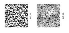
- FIGS. 7A and 7Bshow atomic force microscopy (AFM) micrographs of the top surfaces of active layers.
- a light emitting devicein some cases is a solid state device that converts electrical energy to light.
- a light emitting diode (“LED”)is a light emitting device.
- LEDlight emitting diode
- An LEDmay be a so-called blue LED including a multiple quantum well (MQW) active layer having indium gallium nitride.
- MQWmultiple quantum well
- a blue LEDmay emit non-monochromatic light having a wavelength in a range from about 440 nanometers to 500 nanometers while having an average current density of 38 amperes per square centimeter or more.
- a phosphor coatingmay be provided that absorbs some of the emitted blue light. The phosphor in turn fluoresces to emit light of other wavelengths so that the light the overall LED device emits has a wider range of wavelengths.
- a layerrefers to a layer of atoms or molecules on a substrate.
- a layerincludes an epitaxial layer or a plurality of epitaxial layers (or sub-layers).
- a layermay include a film or thin film.
- a layeris a structural component of a device (e.g., light emitting diode) serving a predetermined device function, such as, for example, an active layer that generates (or emits) light.
- a layergenerally has a thickness from about one monoatomic monolayer (ML) to tens of monolayers, hundreds of monolayers, thousands of monolayers, millions of monolayers, billions of monolayers, trillions of monolayers, or more.
- a layeris a multilayer structure having a thickness greater than one monoatomic monolayer.
- a layermay include multiple material layers.
- a multiple quantum well active layerincludes multiple well and barrier layers.
- coverrefers to the fraction of a surface or interface covered or occupied by a species in relation to the total area of the surface. For example, a coverage of 10% for a species indicates that 10% of a surface is covered by the species. In some situations, coverage is represented by monolayers (ML), with 1 ML corresponding to complete saturation of a surface with a particular species. For example, a pit coverage of 0.1 ML indicates that 10% of a surface is occupied by the openings of pits (or holes). The coverage refers to the surface coverage of such openings (or holes). In an example, for a surface or interface having between about 5% and 30% openings, between about 5% and 30% of the area of the surface or interface is consumed by the openings. In such a case, the opening can be filled by a material, including, but not limited to, a semiconductor material.
- an active regionrefers to a light emitting region of a light emitting diode (LED) that generates light.
- An active layerincludes an active material that generates light upon the recombination of electrons and holes, such as, for example, with the aid of an electrical potential applied across the active layer.
- An active layermay include one or a plurality of layers (or sub-layers).
- an active layerincludes one or more barrier layers (or cladding layers, such as, e.g., GaN) and one or more quantum well (“well”) layers (such as, e.g., InGaN).
- an active layerincludes multiple quantum wells, in which case the active layer may be referred to as a multiple quantum well (“MQW”) active layer.
- MQWmultiple quantum well
- dopedrefers to a structure or layer that is chemically doped.
- a layermay be doped with an n-type chemical dopant (also “n-doped” herein) or a p-type chemical dopant (also “p-doped” herein).
- a layeris undoped or unintentionally doped (also “u-doped”or “u-type” herein).
- a u-GaN (or u-type GaN) layerincludes undoped or unintentionally doped GaN.
- dopantrefers to a chemical dopant, such as an n-type dopant or a p-type dopant.
- P-type dopantsinclude, without limitation, boron, aluminum, magnesium, beryllium, zinc and carbon.
- N-type dopantsinclude, without limitation, nitrogen, phosphorous, silicon, germanium, tin, tellurium and selenium.
- a p-type semiconductoris a semiconductor that is doped with a p-type dopant.
- An n-type semiconductoris a semiconductor that is doped with an n-type dopant.
- n-type Group III-V materialsuch as n-type gallium nitride (“n-GaN”), includes a Group III-V material that is doped with an n-type dopant.
- a p-type Group III-V materialsuch as p-type GaN (“p-GaN”), includes a Group III-V material that is doped with a p-type dopant.
- a Group III-V materialincludes at least one Group III element selected from boron, aluminum, gallium, indium, and thallium, and at least one Group V element selected from nitrogen, phosphorus, arsenic, antimony and bismuth.
- adjacentor “adjacent to,” as used herein, includes ‘next to’, ‘adjoining’, ‘in contact with’, and ‘in proximity to’.
- adjacent componentsare separated from one another by one or more intervening layers.
- the one or more intervening layerscan have a thickness less than about 10 micrometers (“microns”), 1 micron, 500 nanometers (“nm”), 100 nm, 50 nm, 10 nm, 1 nm, or less.
- a first layeris adjacent to a second layer when the first layer is in direct contact with the second layer.
- a first layeris adjacent to a second layer when the first layer is separated from the second layer by a third layer.
- a substraterefers to any workpiece on which film or thin film formation is desired.
- a substrateincludes, without limitation, silicon, silica, sapphire, zinc oxide, carbon (e.g., graphene), SiC, AlN, GaN, spinel, coated silicon, silicon on oxide, silicon carbide on oxide, glass, gallium nitride, indium nitride, titanium dioxide, aluminum nitride, a metallic material (e.g., molybdenum, tungsten, copper, aluminum), and combinations (or alloys) thereof.
- a surfacerefers to the boundary between a first phase and a second phase, such as the boundary between solid phases or the boundary between a solid phase and a gas phase.
- a surfaceis at an interface between a first layer and a second layer.
- the surfacemay be covered by a material layer.
- a surface (or interface)includes openings, such as openings of V-pits. In some situations, the openings are filled with one or more materials.
- injection efficiencyrefers to the proportion of electrons passing through a light emitting device that are injected into the active region of the light emitting device.
- optical quantum efficiencyrefers to the proportion of all electron-hole recombination events in an active region of a light emitting device that are radiative (i.e., producing photons).
- extraction efficiencyrefers to the proportion of photons generated in an active region of a light emitting device that escape from the device.
- EQEexternal quantum efficiency
- Group III-V semiconductor LED'smay be formed of various semiconductor device layers. In some situations, Group III-V semiconductor LED's offer device parameters (e.g., wavelength of light, external quantum efficiency) that may be preferable over other semiconductor materials.
- Gallium nitride (GaN)is a binary Group III-V direct bandgap semiconductor that may be used in optoelectronic applications and high-power and high-frequency devices.
- Group III-V semiconductor based LED'smay be formed on various substrates, such as silicon and sapphire. Silicon provides various advantages over other substrates, such as the capability of using current manufacturing and processing techniques, in addition to using large wafer sizes that aid in maximizing the number of LED's formed within a predetermined period of time. FIG.
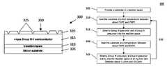
- the LED 100shows an LED 100 having a substrate 105 , an AlGaN layer 110 adjacent to the substrate 105 , pit generation layer 115 adjacent to the AlGaN layer 110 , an n-type GaN (“n-GaN”) layer 120 adjacent to the pit generation layer 115 , an active layer 125 adjacent to the n-GaN layer 120 , an electron blocking (e.g., AlGaN) layer 130 adjacent to the active layer 125 , and a p-type GaN (“p-GaN”) layer 135 adjacent to the electron blocking layer 130 .
- the electron blocking layer 130minimizes the recombination of electrons with holes in the p-GaN layer 135 .
- the substrate 100may be formed of silicon.
- the pit generation layer 115comprises unintentionally doped GaN (“u-GaN”).
- the lattice mismatch and coefficient of thermal expansion between silicon and gallium nitrideleads to structural stresses that generate defects upon the formation of gallium nitride thin films, such as threading and/or hairpin dislocations (collectively “dislocations” herein).
- Thin film growth around the defectsproduces V-defects (or V-pits), which are V-shaped or generally concave structures in device layers.
- V-pitsmake it difficult to achieve uniform device properties, such as the distribution of chemical dopants (“dopants”) in one or more layers.
- the active layermay be formed with low or substantially low defect densities, which may aid in minimizing the coverage (or density) of V-pits.
- Such an approachmay be commercially infeasible and/or difficult to implement with methods currently available for forming LED's.
- the formation of LED component layers (e.g., active layer) at low defect densitiesmay be a slow and resource intensive process, leading to high processing costs and inadequate device turnover to meet the commercial demand for LED devices.
- GaN on silicontypically requires a relatively thick layer of GaN, which may be grown using multiple layers of AlN or SiN x to reduce the dislocation density at the AlN/GaN or SiNx/GaN interface. This makes the run time long, thereby increasing cost, and also makes elimination of cracking difficult due to the thicker GaN layers required. It is typically difficult to form GaN layers on silicon substrates to form light emitting devices having efficiencies comparable to those of GaN layers on sapphire substrates.
- methodsare provided for growing an LED active region over silicon such that high light output efficiencies may be achieved even with relatively high dislocation densities.
- methods provided hereinadvantageously eliminate the need for forming n-GaN layers and active layers with low dislocation densities, such as substantially less than 1 ⁇ 10 9 cm ⁇ 2 , in order to obtain LED's with high light output efficiencies.
- Methods provided hereinmay be used with GaN layers having thicknesses less than 2 ⁇ m.
- the active layer and n-GaN layerhave dislocation densities between about 1 ⁇ 10 8 cm ⁇ 2 and 5 ⁇ 10 9 cm ⁇ 2 .
- the active layer and n-GaN layerhave dislocation densities between about 1 ⁇ 10 9 cm ⁇ 2 and 2 ⁇ 10 9 cm ⁇ 2 .
- LED's having active layers formed over silicon substrates according to methods provided hereinemit light at light output efficiencies similar to, or in some cases exceeding that of, active layers formed over sapphire substrates.
- Device structures and methods for forming active layers for light emitting devices in a manner preferable for moderate to high defect densitiesadvantageously enable the formation of light emitting devices with desirable device properties without the need for minimizing defect densities.
- Methods described in some embodiments of the inventionare based on the unexpected realization that light emitting devices having active layers with moderate to high defect densities may be formed having preferable device performance characteristics by selecting various process parameters during active layer formation to achieve certain V-pit densities and coverages.
- light emitting device structures formed of active layers with relatively moderate to high defect densitiesare provided.
- such active layershave defect densities between about 1 ⁇ 10 8 cm ⁇ 2 and 5 ⁇ 10 9 cm ⁇ 2 .
- such active layershave defect densities between about 1 ⁇ 10 9 cm ⁇ 2 and 2 ⁇ 10 9 cm ⁇ 2 .
- Device structures described in some embodimentspreclude the need to form light emitting device structures with minimal defect densities.
- active layers with relatively moderate to high defect densitiesmay be used, which advantageously reduces processing costs and helps provide for the wide scale use of silicon-based LED's in a commercial setting.
- a light emitting devicesuch as a light emitting diode (LED)
- a first layerwhich includes an n-type Group III-V semiconductor
- a second layerover the first layer.
- the second layerincludes an active material that generates light upon the recombination of electrons and holes.
- the light emitting devicefurther includes a third layer over the second layer.
- the third layerincludes a p-type Group III-V semiconductor.
- the n-type Group III-V semiconductoris n-type gallium nitride (n-GaN) and the p-type Group III-V semiconductor is p-type gallium nitride (GaN)—i.e., GaN doped with an n-type and p-type dopant, respectively.
- the Group III-V semiconductorincludes a Group III species and a Group V species.
- the Group III speciesis gallium and the Group V species is nitrogen.
- the Group III speciesincludes gallium and/or indium.
- the active materialincludes one or more V-pits that have one or more openings at a surface of the active material.
- the density of the V-pitsis between about 1 V-pit/ ⁇ m 2 and 30 V-pits/ ⁇ m 2 , or between about 10 V-pits/ ⁇ m 2 and 20 V-pits/ ⁇ m 2 .
- the V-pit density (or coverage)may be as measured by a surface spectroscopy technique, such as atomic force microscopy (AFM) or scanning tunneling microscopy (STM).
- AFMatomic force microscopy
- STMscanning tunneling microscopy
- the density (or coverage) of openings (or holes) of V-pits at the surface of the second (active) layercorresponds to the density of V-pits in the second layer.
- the active materialincludes one or more V-pits at a density between about 50 V-pits and 500 V-pits in a 25 ⁇ m 2 area, or between about 200 V-pits and 400 V-pits in a 25 ⁇ m 2 area, based on a measurement of the density (e.g., surface density) of openings (or holes) at the surface of the second layer. The density in some cases corresponds to the coverage of holes (or openings) on a surface of the second layer.
- the active materialincludes one or more V-pits at a coverage (e.g., surface coverage) between about 5% and 30%, or between about 10% and 20%.
- the active materialincludes one or more V-pits at a surface coverage between about 0.05 monolayers (ML) and 0.4 ML, or between about 0.1 ML and 0.2 ML.
- the holesare disposed on a surface of the second layer adjacent to the first layer. In other situations, the holes are disposed on a surface of the second layer adjacent to the third layer.
- the active materialin some cases has a dislocation density between about 1 ⁇ 10 8 cm ⁇ 2 and 5 ⁇ 10 9 cm ⁇ 2 , or between about 1 ⁇ 10 9 cm ⁇ 2 and 2 ⁇ 10 9 cm ⁇ 2 (i.e., the number of dislocations in a 1 cm 2 cross-sectional area of the active material).
- the active materialhas a dislocation density greater than or equal to about 1 ⁇ 10 5 cm ⁇ 2 , or greater than or equal to about 1 ⁇ 10 6 cm ⁇ 2 , or greater than or equal to about 1 ⁇ 10 7 cm ⁇ 2 , or greater than or equal to about 1 ⁇ 10 8 cm ⁇ 2 , or greater than or equal to about 1 ⁇ 10 9 cm ⁇ 2 , or greater than or equal to about 2 ⁇ 10 9 cm ⁇ 2 .
- the active layerhas a thickness less than about 1000 nanometers (nm), or less than about 500 nm, or less than about 400 nm, or less than about 300 nm, or less than about 200 nm. In an example, the active layer has a thickness between about 100 nm and 200 nm.
- the first layerhas a thickness between about 100 nm and 8 micrometers (“microns”), or between about 500 nm and 6 microns, or between about 1 micron and 4 microns.
- the thickness of the first layermay be selected so as to provide a light emitting device having predetermined operating conditions.
- the n-type dopantincludes one or more of silicon, germanium, tellurium, selenium and tin. In a particular implementation, the n-type dopant is silicon.
- the third layerhas a thickness between about 10 nm and 1000 nm, or between about 20 nm and 800 nm, or between about 50 nm and 500 nm.
- the thickness of the third layermay be selected so as to provide a light emitting device having predetermined operating conditions.
- the p-type dopantincludes one or more of magnesium, carbon and beryllium. In a particular implementation, the p-type dopant is magnesium.
- the light emitting devicefurther includes a substrate below the first layer or above the third layer.
- the substrateincludes silicon or sapphire, such as an n-type silicon substrate.
- the substrateis for use in the completed light emitting device.
- the substrateis a carrier substrate; the completed light emitting device in such cases will include another substrate.
- the substratehas a thickness between about 100 ⁇ m and 200 ⁇ m.
- the light emitting deviceincludes a pit generation layer.
- the pit generation layeris adjacent to the first layer, such as below the first and second layers. In other cases, the pit generation layer is between the first layer and the second layer. The pit generation layer aids in the growth of the one or more V-pits during the formation of the second layer and, in some cases, other layers formed over the second layer.
- the pit generation layerhas a defect density between about 1 ⁇ 10 8 cm ⁇ 2 and 5 ⁇ 10 9 cm ⁇ 2 . In other embodiments, the pit generation layer has a defect density between about 1 ⁇ 10 9 cm ⁇ 2 and 2 ⁇ 10 9 cm ⁇ 2 . In some embodiments, the pit generation layer has a thickness between about 10 nm and 1000 nm, whereas in other embodiments, the pit generation layer has a thickness between about 50 nm and 500 nm.
- the light emitting deviceincludes an electrode in electrical communication with the first layer by direct contact with the first layer or through one or more intervening layers.
- the light emitting devicefurther includes an electrode in electrical communication with the third layer by direct contact with the third layer or through one or more intervening layers.
- one or both of the electrodeshave shapes and configurations selected to minimize the obstruction of light emanating from the light emitting device.
- the active material of the second layeris a quantum well active material, such as a multiple quantum well (MQW) material.
- the second layerincludes alternating well layers and barrier (or cladding) layers.
- the second layerincludes a well layer formed of indium gallium nitride and/or indium aluminum gallium nitride.
- the barrier layermay be formed of gallium nitride.
- the second layerincludes a well layer formed of aluminum gallium nitride. In such a case, the barrier layer may be formed of aluminum nitride or gallium nitride.
- the material, which includes the active layermay be compositionally graded (also “graded” herein) in two or more elements including the active layer.
- the second layerincludes graded indium gallium nitride, In x Ga 1-x N, wherein ‘x’ is a number between 0 and 1, and a barrier (or cladding) layer formed of GaN.
- the composition of such a layermay vary from a first side to a second side of the second layer.
- a well layerincludes an acceptor material and/or a barrier layer includes a donor material.
- barrier materialsinclude one or more of gallium nitride, aluminum gallium nitride and indium gallium aluminum nitride; well materials include one or more of indium gallium nitride and indium aluminum gallium nitride.
- the stoichiometry of each of the well and barrier layersis selectable to achieve a predetermined device performance, such as the frequency of light emitted by the active layer.
- the second layer(including the active material) has a defect density between about 1 ⁇ 10 8 cm ⁇ 2 and 5 ⁇ 10 9 cm ⁇ 2 , or between about 1 ⁇ 10 9 cm ⁇ 2 and 2 ⁇ 10 9 cm ⁇ 2 .
- the second layermay have a thickness between about 10 nm and 1000 nm, or between about 50 nm and 200 nm.
- the thickness of the light emitting device between the first layer and the second layeris less than about 5 microns, or less than about 4 microns, or less than about 3 microns, or less than about 2 microns, or less than about 1 micron, or less than about 500 nm.
- the light emitting devicehas an external quantum efficiency of at least about 40%, or at least about 50%, or at least about 60%, or at least about 65%, or at least about 70%, or at least about 75%, or at least about 80%, or at least about 85%, or at least about 90%, or at least about 95% at a drive current of about 350 mA.
- the light emitting devicehas an internal quantum efficiency of at least about 40%, or at least about 50%, or at least about 60%, or at least about 65%, or at least about 70%, or at least about 75%, or at least about 80%, or at least about 85%, or at least about 90%, or at least about 95%.
- the light emitting devicehas a low forward voltage of about 2.85 V at 350 mA; a low reverse leakage current at ⁇ 5V of less than about 0.01 ⁇ A; and a wall plug efficiency greater than about 55%.
- an active layer for use in a light emitting diodeincludes a light emitting material having a thickness less than about 500 nanometers and one or more V-pits at a surface density between about 1 V-pit/ ⁇ m 2 and 30 V-pits/ ⁇ m 2 .
- the surface density of the one or more V-pitsis between about 10 V-pits/ ⁇ m 2 and 20 V-pits/ ⁇ m 2 .
- the active layerhas a dislocation density between about 1 ⁇ 10 8 cm ⁇ 2 and 5 ⁇ 10 9 cm ⁇ 2 , or between about 1 ⁇ 10 9 cm ⁇ 2 and 2 ⁇ 10 9 cm ⁇ 2 .
- the active layerincludes one or more layers of a Group III-V material.
- the active layeris a quantum well active layer having a well layer and a barrier layer.
- the active layermay be a multiple quantum well active layer having a plurality of well layers and at least one barrier layer, or a plurality of barrier layers and at least one well layer.
- the active layeris formed of a well layer having indium gallium nitride or aluminum gallium nitride and one or more barrier layers having gallium nitride or aluminum nitride.
- the barrier and well layersare provided in an alternating and sequential fashion, i.e., a barrier layer separating adjacent to well layers, or a well layer separating adjacent to barrier layers.
- the active layerincludes a well layer and a barrier layer adjacent to the well layer.
- the active layermay further include an additional barrier layer adjacent to the well layer or an additional well layer adjacent to the barrier layer.
- Such structuresmay be repeated to form an active layer with any desired number (or periods) of well-barrier stacks, with an individual stack having a well layer adjacent to a barrier layer.
- the active layerincludes at least one period, or at least 5 periods, or at least 10 periods, or at least 20 periods, or at least 30 periods, or at least 40 periods, or at least 50 periods, or at least 60 periods, or at least 70 periods, or at least 80 periods, or at least 90 periods, or at least 100 periods.
- a well layeris thinner than a barrier layer.
- an InGaN well layerhas a thickness between about 1 nm and 20 nm, or 2 nm and 10 nm
- a GaN barrier layerhas a thickness between about 5 nm and 30 nm, or 10 nm and 20 nm.
- the barrier layermay be disposed between well layers, or a well layer may be disposed between two barrier layers.
- an active layer for use in a light emitting deviceincludes a light emitting material having a thickness less than about 500 nm, or less than about 400 nm, or less than about 300 nm, or less than about 200 nm.
- the active layerhas one or more V-pits at surface coverage between about 5% and 30%. In some cases, the surface coverage is between about 10% and 20%.
- an LEDincludes an n-type gallium nitride (GaN) layer, a p-type GaN layer, and an active layer between the n-type GaN layer and the p-type GaN layer, the active layer having one or more V-pits at a surface density between about 5% and 30%.
- the LEDhas a substrate adjacent to the n-type GaN layer or p-type GaN layer. The substrate is in contact with either the n-GaN layer or the p-GaN layer, or adjacent to the n-GaN layer or p-GaN layer but separated from the n-GaN layer or p-GaN by one or more intervening layers.
- the substratemay be formed of sapphire or silicon (e.g., n-type silicon).
- the active layerin some cases, includes one or more quantum well stacks. Each of the quantum well stacks includes a barrier layer and a well layer adjacent to the barrier layer.
- the active layerhas a thickness less than about 500 nm, or less than about 400 nm, or less than about 300 nm, or less than about 200 nm.
- the performance of a light emitting devicedepends on the thickness of the active layer and the distribution (or coverage) of V-pits on a surface of the active layer. In some situations, the performance of a light emitting device can be optimized by selecting a thickness of the active layer that gives a predetermined distribution and/or coverage of V-pits during active layer (epitaxial) growth. In an example, for a light emitting device having a dislocation density between about 1 ⁇ 10 9 cm ⁇ 2 and 2 ⁇ 10 9 cm ⁇ 2 , an active layer having a thickness between about 50 nm and 200 nm provides a V-pit coverage that is between about 10% and 20%.
- the performance of such a devicemay be preferable in relation to a device having a thicker active layer or V-pit surface coverage below 10% or above 20%.
- an active layer having a thickness of about 150 nm and a V-pit surface coverage of about 10%has a light output efficiency that is increased by at least about 40% in relation to a device having an active layer with a thickness of about 300 nm and a V-pit coverage of 30%.
- the V-pit coverage for a particular active layer thicknessmay be a function of growth conditions of the active layer (see below).
- FIG. 2shows a device 200 having a silicon substrate 205 , one or more transition layers 210 on the silicon substrate 205 , and an n-type Group III-V semiconductor layer 215 on the one or more transition layers, in accordance with an embodiment.
- the one or more transition layersinclude one or more u-type Group III-V semiconductor (i.e., an undoped or unintentionally doped Group III-V semiconductor, such as, e.g., unintentionally doped GaN) layers and/or one or more strain relaxation layers, such as a doped Group III-V semiconductor layer (e.g., aluminum gallium nitride) with a lattice constant between the silicon substrate 205 and the n-type Group III-V semiconductor layer 215 .
- a doped Group III-V semiconductor layere.g., aluminum gallium nitride
- the one or more transition layers 210include an AlGaN layer and a u-GaN layer over the AlGaN layer, the u-GaN layer disposed adjacent to the n-type Group III-V semiconductor layer.
- the Group III-V semiconductor materialis gallium nitride (GaN).
- the n-type Group III-V layer 215includes n-type gallium nitride (n-GaN).
- the n-type Group III-V layerincludes an n-type dopant, such as, for example, silicon.
- the silicon substrate 205has a (111) crystallographic orientation (i.e., the silicon substrate is Si(111)). In other examples, the silicon substrate 205 has other crystallographic orientations.
- the silicon substrate 205may have facets and defects (e.g., steps) exhibiting one or more other crystallographic planes, such as, for example, a (100) crystallographic plane. In some cases, a substrate having a (111)-oriented surface has defects (e.g., steps) exhibiting other orientations.
- FIG. 3shows a device 300 having a silicon substrate 305 , one or more transition layers 310 on the silicon substrate 305 , an n-type Group III-V semiconductor layer 315 on the one or more transition layers, and an active layer 320 on the n-type Group III-V semiconductor layer, in accordance with an embodiment of the invention.
- the active layer 320generates light upon the recombination of electrons and holes, such as, for example, upon the application of an electrical potential (voltage) across the active layer 320 with the aid of contacts or electrodes in electrical communication with the n-type Group III-V layer 315 and a p-type Group III-V layer (see, e.g., FIG. 1 ) over the active layer 320 .
- the one or more transition layer 310may be as described above in the context of FIG. 2 .
- the active layer 320includes one or more quantum wells and barrier layers.
- the active layer 320is formed of a MQW material.
- the active layer 320may be formed of one or more aluminum gallium nitride (AlGaN) quantum well layers and an aluminum nitride (AlN) well layer separating the one or more AlGaN quantum well layers.
- AlGaNaluminum gallium nitride
- AlNaluminum nitride
- the active layer 320may have a defect density between about 1 ⁇ 10 8 cm ⁇ 2 and 5 ⁇ 10 9 cm ⁇ 2 , or between about 1 ⁇ 10 9 cm ⁇ 2 and 2 ⁇ 10 9 cm ⁇ 2 .
- the active layer 320 of the device 300includes a plurality of V-pits 325 extending from the n-type Group III-V semiconductor layer 315 to a top surface 330 of the active layer 320 .
- the V-pits (or V-defects)are formed on or around defects (e.g., dislocations) in the n-type Group III-V semiconductor layer 315 .
- the density of V-pits at the top surface 330 of the active layer 320is between about 1 V-pit/ ⁇ m 2 and 30 V-pits/ ⁇ m 2 , or between about 10 V-pits/ ⁇ m 2 and 20 V-pits/ ⁇ m 2 .
- the active layer 320has between about 50 V-pits and 500 V-pits in a 25 ⁇ m 2 area (of the top surface 330 ), or between about 200 V-pits and 400 V-pits in a 25 ⁇ m 2 area.
- the V-pits 325have a surface coverage between about 0.05 monolayers (ML) and 0.4 ML, or between about 0.1 ML and 0.2 ML.
- the V-pit density and coveragemay be as measured with the aid of a surface analytical technique, such as an AFM or STM.
- STM or AFMmay be used to measure the density of openings (or holes) at the surface of an active layer, and the density of openings may correspond to the density of V-pits in the active layer 320 .
- the device 300may include additional layers over the active layer 320 .
- the device 300includes a p-type Group III-V semiconductor layer over the active layer 320 .
- the device 300includes an electron blocking layer between the active layer 320 and the p-type Group III-V semiconductor layer.
- the p-type Group III-V semiconductor layeris formed of p-type GaN (p-GaN).
- the electron blocking layermay be formed of aluminum gallium nitride.
- FIG. 4schematically illustrates an active layer 400 having a top surface 405 , in accordance with an embodiment of the invention.
- the top surface 405has a first width (W 1 ) and a second width (W 2 ).
- the first width and the second width, as illustrated,are substantially the same.
- the top surface 405includes the openings of a plurality of pits 410 .
- the pits 410are V-pits, such as those discussed above in the context of FIG. 3 .
- the pits 410extend into the active layer 400 and, in some cases, extend to a layer below the active layer 400 , such as an n-type Group III-V semiconductor layer (not shown).
- the pits 410may have various cross-sectional areas.
- the pits 410may form at or near defects in the active layer 400 and/or one or more layers below the active layer.
- At least some of the pitsgrow in size. For instance, the diameters (and cross-sectional areas) of at least some of the pits increase with increasing thickness of the active layer.
- two or more pitscoalesce to form a single opening at the top surface 405 of the active layer 400 .
- the pitsmay have various diameters, shapes and configuration.
- the openings of pits 410have diameters that are between 1 nm and 2000 nm, or between about 10 nm and 1000 nm, or between about 60 nm and 120 nm, or between about 80 nm and 100 nm.
- the openings of pits 410have diameters that are less than about 2000 nm, or less than about 1000 nm, or less than about 500 nm, or less than about 400 nm, or less than about 300 nm, or less than about 200 nm, or less than about 100 nm, or less than about 90 nm, or less than about 80 nm, or less than about 70 nm, or less than about 65 nm.
- the top surface 405may include pits of various sizes. In an example, some pits 410 are smaller than others. In another example, the pits 410 have substantially similar sizes. Some pits may completely extend through the active layer 400 , while other pits may extend through a portion of the active layer 400 (e.g., 50% through the active layer).
- pitsmay grow along a vector parallel to an axis orthogonal to the top surface 405 (“surface normal”, extending out of the plane of the figure), while other pits may grow along a vector that is at an angle with respect to the surface normal, such as greater than about 0°, or greater than about 5°, or greater than about 10°, or greater than about 20°, or greater than about 30°, or greater than about 40°, or greater than about 50°, or greater than about 60° with respect to the surface normal. In some cases, pit sidewall facets are about 60°.
- the pitshave cross-sections (or openings) that are circular, triangular, square, rectangular, pentagonal, hexagonal, heptagonal, nonagonal, or combinations thereof.
- the openingare partial segments (e.g., semi-circular, semi-rectangular) of these shapes.
- the pitsare filled with one or more materials, such as a Group III-V semiconductor.
- the openings of pitscan be filled with the one or more materials.
- active layer 400has a thickness that is less than or equal to about 200 nm, or less than or equal to about 150 nm, and a dislocation density between about 1 ⁇ 10 9 cm ⁇ 2 and 2 ⁇ 10 9 cm ⁇ 2 .
- methods for forming a light emitting deviceare provided. Methods provided herein enable the formation of light emitting device active layers that are optimized for use in situations in which the active layers have dislocations densities between about 1 ⁇ 10 8 cm ⁇ 2 and 5 ⁇ 10 9 cm ⁇ 2 , or between about 1 ⁇ 10 9 cm ⁇ 2 and 2 ⁇ 10 9 cm ⁇ 2 .
- a method for forming a light emitting deviceincludes forming an n-type or p-type Group III-V semiconductor layer adjacent to an active layer.
- the active layeris formed by exposing a substrate in a reaction chamber to one or more Group III precursors and one or more Group V precursors at one or more growth conditions selected to generate one or more V-pits in the active layer at a surface density between about 1 V-pit/ ⁇ m 2 and 30 V-pits/ ⁇ m 2 , or between about 10 V-pits/ ⁇ m 2 and 20 V-pits/ ⁇ m 2 .
- the Group III-V semiconductorincludes gallium nitride (GaN).
- the substrateincluding any layer over the substrate is contacted with the one or more Group III precursors and the one or more Group V precursors.
- an active layer including gallium nitride barrier layers and indium gallium nitride or indium aluminum gallium nitride well layersis formed over an n-GaN layer over a silicon substrate in a reaction chamber.
- the growth temperature and carrier gas (e.g., H 2 ) flow rateare selected to generate an active layer having a V-pit surface coverage between about 5% and 30%, or between about 10% and 20%.
- such growth conditionsare selected to maintain a dislocation density between about 1 ⁇ 10 8 cm ⁇ 2 and 5 ⁇ 10 9 cm ⁇ 2 , or between about 1 ⁇ 10 9 cm ⁇ 2 and 2 ⁇ 10 9 cm ⁇ 2 .
- the n-GaN layeris formed over one or more additional layers (e.g., pit generation layer) over the silicon substrate.
- the n-GaN layeris formed using growth conditions selected to provide a dislocation density between about 1 ⁇ 10 8 cm ⁇ 2 and 5 ⁇ 10 9 cm ⁇ 2 , or between about 1 ⁇ 10 9 cm ⁇ 2 and 2 ⁇ 10 9 cm ⁇ 2 in the n-GaN layer.
- a Group III-V semiconductorincludes one or more Group III species and one or more Group-V species.
- the Group III speciesis gallium (Ga) and the Group V species is nitrogen.
- An n-type Group III-V semiconductoris a Group III-V semiconductor that is doped with an n-type dopant (e.g., Si).
- a p-type Group III-V semiconductoris a Group III-V semiconductor that is doped with a p-type dopant (e.g., Mg).
- the reaction chambermay be a vacuum chamber configured for thin film formation.
- the vacuum chamberin some cases, is an ultrahigh vacuum (UHV) chamber.
- the reaction chambermay be pumped with the aid of a pumping system having one or more vacuum pumps, such as one or more of a turbomolecular (“turbo”) pump, a cryopump, an ion pump and a diffusion pump and a mechanical pump.
- the reaction chambermay include a control system for regulating precursor flow rates, substrate temperature, chamber pressure, and the evacuation of the chamber.
- the reaction chambermay be part of a system configured to generate the light emitting device (see, e.g., FIG. 6 ).
- growth conditionsare adjustable based upon the selection of one or more process parameters for forming the active layer and/or layers above and below the active layer.
- growth conditionsinclude one or more of growth temperature, carrier gas flow rate, precursor flow rate, growth rate and growth pressure.
- processing parameters provided hereinare used for cases in which an active layer having a Group III-V semiconductor at a moderate to high dislocation density is formed over a silicon substrate.
- the dislocation densityis some situations is between about 1 ⁇ 10 8 cm ⁇ 2 and 5 ⁇ 10 9 cm ⁇ 2 , or between about 1 ⁇ 10 9 cm ⁇ 2 and 2 ⁇ 10 9 cm ⁇ 2 .
- one or more processing parameters for forming an active layerare adjusted to provide an active layer having a V-pit density provided herein, such as between about 5% and 30%, or between about 10% and 20%, at a dislocation density between about 1 ⁇ 10 8 cm ⁇ 2 and 5 ⁇ 10 9 cm ⁇ 2 , or between about 1 ⁇ 10 9 cm ⁇ 2 and 2 ⁇ 10 9 cm ⁇ 2 .
- active layer growth conditionsare selected to provide a V-pit surface density between about 5% and 30%, or between about 10% and 20%, at an active layer thickness less than or equal to about 300 nm, or less than or equal to about 200 nm, or less than or equal to about 150 nm, and at an active layer dislocation density between about 1 ⁇ 10 8 cm ⁇ 2 and 5 ⁇ 10 9 cm ⁇ 2 , or between about 1 ⁇ 10 9 cm ⁇ 2 and 2 ⁇ 10 9 cm ⁇ 2 .
- the growth temperature and carrier gas (e.g., H 2 ) flow rateare selected to achieve a predetermined density and/or distribution of V-pits.
- the growth temperatureis the temperature of substrate or one or more layers over the substrate upon thin film formation.
- the growth temperatureis the substrate temperature, as measured with the aid of a pyrometer or a thermocouple in thermal contact with the substrate.
- the temperature of the substrateis between about 750° C. and 850° C.
- the active layerincludes a quantum wall material, such as a multiple quantum well (MQW) material having a well layer and a barrier layer.
- MQWmultiple quantum well
- the well layeris formed at a temperature between about 750° C. and 790° C., or between about 770° C. and 780° C.
- the barrier layeris formed at a temperature between about 790° C. and 850° C., or between about 810° C. and 840° C.
- the precursor flow rateincludes the flow rate of one or more Group III precursors and the flow rate of a Group V precursor.
- the flow ratespecifies the volume of precursor delivered to a reaction chamber within a predetermined period of time.
- a gallium precursormay include one or more of trimethylgallium (TMG), triethylgallium, diethylgallium chloride and coordinated gallium hydride compounds (e.g., dimethylgallium hydride).
- An aluminum precursormay include one or more of tri-isobutyl aluminum (TIBAL), trimethyl aluminum (TMA), triethyl aluminum (TEA), and dimethylaluminum hydride (DMAH).
- An indium source gasmay include one or more of trimethyl indium (TMI) and triethyl indium (TEI).
- a nitrogen precursormay include one or more of ammonia (NH 3 ), nitrogen (N 2 ), and plasma-excited species of ammonia and/or N 2 .
- one or more precursorare provided to a reaction chamber with the aid of a carrier gas including one or more of He, Ar, N 2 and H 2 .
- a carrier gasincluding one or more of He, Ar, N 2 and H 2 .
- the flow rate of the carrier gas during the formation of the active layeris between about 1 liter/minute and 20 liters/minute.
- the active layeris formed by exposing a substrate in a reaction chamber to one or more precursors and hydrogen (H 2 ).
- the flow rate of hydrogen during the formation of the active layeris between about 1 liter/minute and 20 liters/minute, or between about 1 liter/minute and 10 liters/minute, or between about 4 liters/minute and 8 liters/minute.
- the hydrogen flow rateis adjusted based on whether a well layer or barrier layer is being formed.
- the hydrogen flow rateis between about 1 liter/minute and 10 liters/minute, or between about 4 liters/minute and 8 liters/minute.
- the hydrogen flow rateis reduced in relation to the flow rate of hydrogen during the formation of the barrier layer. In some situations, the flow rate of hydrogen during the formation of the well layer is terminated (i.e., at or near about 0 liters/minute).
- the well layeris formed at a temperature (growth temperature) between about 750° C. and 790° C., or between about 770° C. and 780° C.
- the barrier layeris formed at a temperature between about 790° C. and 850° C., or between about 810° C. and 840° C., and at a hydrogen flow rate between about 1 liter (L)/minute (min) and 10 L/min, or between about 4 L/min and 8 L/min.
- the barrier layeris formed at a temperature of about 820° C.
- the hydrogen flow rate during the formation of the well layeris terminated.
- the growth temperature for the barrier layerscales inversely with increasing hydrogen flow rate. That is, the higher the hydrogen flow rate, the lower the growth temperature.
- the temperature for the formation of the well layeris 30° C. to 40° C. below the temperature for the formation of the barrier layer.
- a barrier layeris formed over a silicon substrate in a reaction chamber by flowing TMG, NH 3 and H 2 into the reaction chamber at an H 2 flow rate of about 6 liters/minute. After a predetermined period of time, the H 2 flow rate is terminated and an indium precursor is introduced into the reaction chamber along with TMG and NH 3 to form a well layer. Such operations may be repeated as desired to form a multiple quantum well layer with a period (i.e., the number of barrier-well stacks) as desired.
- the growth rateis the rate of growth of various device layers, such as the active layer.
- the growth rateis dependent on the precursor flow rate. That is, the higher the flow rate of precursor into the reaction chamber, the higher the growth rate.
- the growth rateis dependent on the flow rate of hydrogen. In other situations, the growth rate depends on one or more factors selected from precursor flow rate, hydrogen flow rate, carrier gas flow rate, reaction chamber pressure and growth temperature.
- a method for forming a light emitting diodeincludes forming an active layer by exposing a substrate in a reaction chamber to a Group III precursor and a Group V precursor to form an active layer having one or more V-pits at a surface density between about 1 V-pit/ ⁇ m 2 and 30 V-pits/ ⁇ m 2 , or between about 10 V-pits/ ⁇ m 2 and 20 V-pits/ ⁇ m 2 .
- the temperature of the substrateis between about 750° C. and 850° C.
- the flow rate of hydrogen (H 2 ) into the reaction chamberis less than or equal to about 20 liters/minute.
- the temperature of the substrateis between about 750° C. and 850° C.
- the flow rate of hydrogen (H 2 ) into the reaction chamberis less than or equal to about 20 liters/minute. In some situations, the flow rate of hydrogen is less than about 10 liters/minute.
- substrateincludes a substrate with or without additional material layers over the substrate.
- exposing the substrate, in the reaction chamber, to a Group III precursor and a Group V precursorincludes exposing one or more layers over the substrate to the Group III precursor and the Group V precursor.
- exposing the substrate, in the reaction chamber, to a Group III precursor and a Group V precursorincludes exposing the substrate to the Group III precursor and the Group V precursor.
- the substrateincludes a layer of an n-type or p-type Group III-V material, and the active layer is formed over the layer of the n-type or p-type Group III-V material.
- the active layeris formed over an n-GaN layer formed over a silicon substrate.
- the substrateis exposed to (and in some cases contacted with) the Group III precursor and the Group V precursor simultaneously. In other situations, during the formation of the active layer the substrate is exposed to the Group III precursor and the Group V in an alternating fashion (e.g., the Group III precursor followed by the Group V precursor).
- a method for forming a light emitting diodeincludes providing a substrate in a reaction chamber and heating the substrate at a first temperature between about 750° C. and 790° C. A well layer is then formed on or over the substrate by directing into the reaction chamber a Group III precursor and a Group V precursor, wherein the well layer is formed at a first carrier gas flow rate. In some situations, other precursors are directed into the reaction chamber to form the well layer. Next, the substrate is heated at a temperature between about 790° C. and 850° C. and a barrier layer is formed adjacent to the well layer by directing into the reaction chamber the Group III precursor and the Group V precursor. The barrier layer is formed at a second carrier gas flow rate. In some cases, the first carrier gas flow rate is less than the second carrier gas flow rate.
- the second carrier gas flow rateis between about 1 liter/minute and 10 liters/minute, or between about 4 liters/minute and 8 liters/minute.
- the carrier gasmay include one or more of hydrogen (H 2 ), nitrogen (N 2 ), argon (Ar) and Helium (He).
- the carrier gasis hydrogen.
- the carrier gasaids in the growth of the barrier layer and/or the well layer.
- the carrier gasis used during the formation of the barrier layer but not the well layer.
- the flow rate of hydrogenis between about 1 liter/minute and 10 liters/minute, or between about 4 liters/minute and 8 liters/minute. In such a case, during the formation of the well layer, the flow rate of hydrogen may be reduced or terminated.
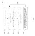
- FIG. 5schematically illustrates a method 500 for forming a quantum well active layer for a light emitting device, in accordance with an embodiment of the invention.
- a substrateis provided in a reaction chamber.
- the substrateis selected to have a moderate to high dislocation density between about 1 ⁇ 10 8 cm ⁇ 2 and 5 ⁇ 10 9 cm ⁇ 2 , or between about 1 ⁇ 10 9 cm ⁇ 2 and 2 ⁇ 10 9 cm ⁇ 2 .
- the substrateis silicon (e.g., n-type silicon).
- the substrateis heated at a first temperature between about 750° C. and 790° C. In some situations, the first temperature is between about 770° C. and 780° C.
- the substratemay be heated with the aid of a resistive heating, such as with the aid of a susceptor adjacent to the substrate.
- the temperature of the substratemay be adjusted from an initial temperature at a predetermined heating or cooling rate.
- a well layeris formed over the substrate by directing into the reaction chamber one or more well layer precursors.
- the well layerincluding a Group-III-V material
- one or more Group III precursors and one or more Group V precursorsare directed into the reaction chamber to form a well layer having a Group III-V semiconductor.
- the substrateis exposed to the one or more precursors at the first temperature until a well layer of predetermined thickness is formed.
- the Group III-V semiconductor of the well layerincludes indium gallium nitride, and the well layer is formed by directing trimethyl indium (TMI), trimethyl gallium (TMG), and NH 3 and/or nitrogen (N 2 ) in to the reaction chamber.
- the Group III-V semiconductor of the well layerincludes aluminum gallium nitride, and the well layer is formed by directing trimethyl aluminum (TMA), TMG, and NH 3 and/or N 2 into the reaction chamber.
- the substrateis heated at a second temperature between about 790° C. and 850° C.
- the second temperatureis between about 810° C. and 840° C.
- the temperature of the substratemay be adjusted from the first temperature to the second temperature at a predetermined heating rate. For instance, the temperature of the substrate may be increased from the first temperature to the second temperature at a heating rate between about 0.1° C./second and 10° C./second, or between about 0.5° C./second and 5° C./second. In an example, the heating rate is about 1° C./second.
- a barrier layeris formed over the substrate by directing into the reaction chamber one or more barrier layer precursors and hydrogen (H 2 ).
- the barrier layerincludes a Group III-V species.
- a Group III precursor, a Group V precursor and hydrogen (H 2 )are directed into the reaction chamber.
- the substrateis exposed to the one or more barrier layer precursors and H 2 at the second temperature until a barrier layer of predetermined thickness is formed.
- the flow rate of hydrogenis between about 1 liter/minute (L/min) and 10 L/min, or between about 4 L/min and 8 L/min.
- a Group III precursor, Group V precursor and H 2are directed into the reaction chamber.
- Group III-V semiconductorincludes gallium nitride
- the Group III precursorincludes a gallium source gas, such as TMG
- the Group V precursorincludes NH 3 or nitrogen (N 2 ).
- the flow rate of hydrogen in such a caseis between about 1 L/min and 10 L/min, such as, e.g., 6 L/min.
- the operations 510 - 525may be repeated 530 to form an active layer with a predetermined period of well-barrier stacks.
- the operations 510 - 525are repeated once, twice, three times, four times, five times, six times, or seven times to form a MQW active layer.
- one or more additional layersare formed over the substrate.
- an n-type Group III-V semiconductor layeris formed over the substrate prior to forming the active layer with the aid of operations 510 - 530 .
- one or more layersare formed on the active layer.
- a p-type Group III-V semiconductor layeris formed on the active layer.
- one or more additional layersare formed over the active layer.
- a p-type Group III-V semiconductor layeris formed over the active layer.
- the p-type Group III-V semiconductor layerincludes p-type GaN. Additional front side and/or back side contacts are also formed to provide an electric flow path to the n-type Group III-V semiconductor layer and the p-type Group III-V semiconductor layer.
- One or more layers of light emitting devices provided hereinmay be formed by a vapor (or gas phase) deposition technique.
- one or more layers of the light emitting devices provided hereinare formed by chemical vapor deposition (CVD), atomic layer deposition (ALD), plasma enhanced CVD (PECVD), plasma enhanced ALD (PEALD), metal organic CVD (MOCVD), hot wire CVD (HWCVD), initiated CVD (iCVD), modified CVD (MCVD), vapor axial deposition (VAD), outside vapor deposition (OVD) and/or physical vapor deposition (e.g., sputter deposition, evaporative deposition).
- CVDchemical vapor deposition
- ALDatomic layer deposition
- PECVDplasma enhanced CVD
- PEALDplasma enhanced ALD
- MOCVDmetal organic CVD
- HWCVDhot wire CVD
- iCVDinitiated CVD
- MCVDmodified CVD
- VADvapor axial deposition
- OTDvapor de
- GaNgallium nitride
- GaAsgallium arsenide
- AlGaAsaluminum gallium arsenide
- GaAsPgallium arsenide phosphide
- AlGaInPaluminum gallium indium phosphide
- GaPgallium phosphide
- InGaNaluminum gallium phosphide
- ZnSezinc selenide
- AlNaluminum nitride
- AlGaNaluminum gallium nitride
- AlGaNaluminum gallium nitride
- AlGaInNaluminum gallium indium nitride
- a system for forming a light emitting deviceincludes a reaction chamber for holding a substrate, a pumping system in fluid communication with the reaction chamber, the pumping system configured to purge or evacuate the reaction chamber, and a computer system having a processor for executing machine readable code implementing a method for forming an active layer.
- the codemay implement any of the methods provided herein.
- the codeimplements a method including forming an active layer by exposing the substrate in the reaction chamber to a Group III precursor and a Group V precursor to form an active layer having one or more V-pits at a surface density between about 1 V-pit/ ⁇ m 2 and 30 V-pits/ ⁇ m 2 , or between about 10 V-pits/ ⁇ m 2 and 20 V-pits/ ⁇ m 2 .
- the temperature of the substrateis between about 750° C. and 850° C.
- the flow rate of hydrogen (H 2 ) into the reaction chamberis less than or equal to about 20 liters/minute.
- FIG. 6shows a system 600 for forming a light emitting device, in accordance with an embodiment of the invention.
- the system 600includes a reaction chamber 605 having a susceptor (or substrate holder) 610 configured to hold a substrate that is used to form the light emitting device.
- the systemincludes a first precursor storage vessel (or tank) 615 , a second precursor storage vessel 620 , and a carrier gas storage tank 625 .
- the first precursor storage vessel 615may be for holding a Group III precursor (e.g., TMG) and the second precursor storage vessel 620 may be for holding a Group V precursor (e.g., NH 3 ).
- the carrier gas storage tank 625is for holding a carrier gas (e.g., H 2 ).
- the system 600may include other storage tanks or vessels, such as for holding additional precursors and carrier gases.
- the system 600further includes a vacuum system 630 for providing a vacuum to the reaction chamber 605 .
- the vacuum system 630is in fluid communication with the reaction chamber 605 .
- the vacuum system 630is configured to be isolated from the reaction pace 605 with the aid of a valve, such as a gate valve.
- a controller (or control system) 635 of the system 600implements a method for forming a light emitting device in the reaction chamber 605 , such as forming one or more layers of the light emitting device.
- the controller 635is communicatively coupled to a valve of each of the first precursor storage vessel 615 , the second precursor storage vessel 620 , the carrier gas storage tank 625 and the vacuum system 630 .
- the controller 635is operatively coupled to the susceptor 610 for regulating the temperature of the susceptor and a substrate on the susceptor, and the vacuum system 630 for regulating the pressure in the reaction chamber 605 .
- the vacuum system 630includes one or more vacuum pumps selected from a turbomolecular (“turbo”) pump, a cryopump, an ion pump and a diffusion pump and a mechanical pump.
- a pumpmay include one or more backing pumps.
- a turbo pumpmay be backed by a mechanical pump.
- the controller 635is configured to regulate one or more processing parameters, such as the substrate temperature, precursor flow rates, growth rate, hydrogen flow rate and reaction chamber pressure.
- the controller 635includes a processor configured to aid in executing machine-executable code that is configured to implement the methods provided herein.
- the machine-executable codeis stored on a physical storage medium, such as flash memory, a hard disk, or other physical storage medium configured to hold computer-executable code.
- the controller 635is configured to regulate one or more processing parameters to generate an active layer with a V-pit surface density (or coverage) between about 5% and 30%, or between about 10% and 20%, at an active layer thickness less than or equal to about 300 nm, or less than or equal to about 200 nm, or less than or equal to about 150 nm, and at an active layer dislocation density between about 1 ⁇ 10 8 cm ⁇ 2 and 5 ⁇ 10 9 cm ⁇ 2 , or between about 1 ⁇ 10 9 cm ⁇ 2 and 2 ⁇ 10 9 cm ⁇ 2 .
- V-pit surface densityor coverage
- FIG. 7Ais an AFM micrograph of a 5 ⁇ m ⁇ 5 ⁇ m surface of an active layer formed on silicon (Sample A).
- the active region of Sample Ahas a thickness of about 300 nm.
- FIG. 7Bis an AFM micrograph of a 5 ⁇ m ⁇ 5 ⁇ m surface of an active layer formed on silicon (Sample B).
- the active region of Sample Bhas a thickness of about 150 nm.
- the active layers of Sample A and Sample Bhave dislocation densities between about 1 ⁇ 10 9 cm ⁇ 2 and 2 ⁇ 10 9 cm ⁇ 2 .
- the surface of Sample Ahas a V-pit surface coverage of about 30%, and the surface of Sample B has a V-pit surface coverage of about 10%.
- LED'sare formed on silicon having active layers with thicknesses and V-pit surface coverages of Samples A and B.
- An LED having the active layer of Sample Bhas a light output efficiency that is about 40% higher than an LED having the active layer of Sample A.
- FIGS. 7A and 7Billustrate that LED's with highly dislocated materials and thinner active regions are more efficient light generators than LED's with highly dislocated materials and thicker active regions.
- words using the singular or plural numberalso include the plural or singular number respectively.
- words ‘herein,’ ‘hereunder,’ ‘above,’ ‘below,’ and words of similar importrefer to this application as a whole and not to any particular portions of this application.
- word ‘or’is used in reference to a list of two or more items, that word covers all of the following interpretations of the word: any of the items in the list, all of the items in the list and any combination of the items in the list.
Landscapes
- Led Devices (AREA)
Abstract
Description
Claims (28)
Priority Applications (8)
| Application Number | Priority Date | Filing Date | Title |
|---|---|---|---|
| US13/249,146US8853668B2 (en) | 2011-09-29 | 2011-09-29 | Light emitting regions for use with light emitting devices |
| KR1020137023524AKR20130132600A (en) | 2011-09-29 | 2012-09-27 | Light emitting regions for use with light emitting devices |
| JP2014510556AJP5895048B2 (en) | 2011-09-29 | 2012-09-27 | Method for forming light emitting diode |
| PCT/US2012/057663WO2013049416A2 (en) | 2011-09-29 | 2012-09-27 | Light emitting regions for use with light emitting devices |
| KR1020157020656AKR20150093860A (en) | 2011-09-29 | 2012-09-27 | Light emitting regions for use with light emitting devices |
| CN201280011989.5ACN103430333B (en) | 2011-09-29 | 2012-09-27 | Light-emitting zone for light-emitting device |
| TW101135816ATW201330319A (en) | 2011-09-29 | 2012-09-28 | Light-emitting device with light-emitting area |
| US14/473,672US20150056731A1 (en) | 2011-09-29 | 2014-08-29 | Light emitting regions for use with light emitting devices |
Applications Claiming Priority (1)
| Application Number | Priority Date | Filing Date | Title |
|---|---|---|---|
| US13/249,146US8853668B2 (en) | 2011-09-29 | 2011-09-29 | Light emitting regions for use with light emitting devices |
Related Child Applications (1)
| Application Number | Title | Priority Date | Filing Date |
|---|---|---|---|
| US14/473,672DivisionUS20150056731A1 (en) | 2011-09-29 | 2014-08-29 | Light emitting regions for use with light emitting devices |
Publications (2)
| Publication Number | Publication Date |
|---|---|
| US20130082236A1 US20130082236A1 (en) | 2013-04-04 |
| US8853668B2true US8853668B2 (en) | 2014-10-07 |
Family
ID=47991711
Family Applications (2)
| Application Number | Title | Priority Date | Filing Date |
|---|---|---|---|
| US13/249,146Expired - Fee RelatedUS8853668B2 (en) | 2011-09-29 | 2011-09-29 | Light emitting regions for use with light emitting devices |
| US14/473,672AbandonedUS20150056731A1 (en) | 2011-09-29 | 2014-08-29 | Light emitting regions for use with light emitting devices |
Family Applications After (1)
| Application Number | Title | Priority Date | Filing Date |
|---|---|---|---|
| US14/473,672AbandonedUS20150056731A1 (en) | 2011-09-29 | 2014-08-29 | Light emitting regions for use with light emitting devices |
Country Status (6)
| Country | Link |
|---|---|
| US (2) | US8853668B2 (en) |
| JP (1) | JP5895048B2 (en) |
| KR (2) | KR20150093860A (en) |
| CN (1) | CN103430333B (en) |
| TW (1) | TW201330319A (en) |
| WO (1) | WO2013049416A2 (en) |
Cited By (1)
| Publication number | Priority date | Publication date | Assignee | Title |
|---|---|---|---|---|
| US9490392B2 (en) | 2011-09-29 | 2016-11-08 | Toshiba Corporation | P-type doping layers for use with light emitting devices |
Families Citing this family (13)
| Publication number | Priority date | Publication date | Assignee | Title |
|---|---|---|---|---|
| US20130082274A1 (en) | 2011-09-29 | 2013-04-04 | Bridgelux, Inc. | Light emitting devices having dislocation density maintaining buffer layers |
| US9557215B2 (en) | 2012-08-17 | 2017-01-31 | Massachusetts Institute Of Technology | Phonon-recyling light-emitting diodes |
| DE102012217640B4 (en)* | 2012-09-27 | 2020-02-20 | Osram Opto Semiconductors Gmbh | Optoelectronic component and method for its production |
| EP3033776A4 (en) | 2013-08-16 | 2017-01-25 | Massachusetts Institute of Technology | Thermo-electrically pumped light-emitting diodes |
| KR20150025264A (en) | 2013-08-28 | 2015-03-10 | 삼성전자주식회사 | Semiconductor light emitting device including hole injection layer |
| KR20150078641A (en)* | 2013-12-31 | 2015-07-08 | 일진엘이디(주) | Nitride semiconductor light emitting device with v-pit and method of manufacturing the same |
| TWI577046B (en)* | 2014-12-23 | 2017-04-01 | 錼創科技股份有限公司 | Semiconductor light emitting element and manufacturing method thereof |
| DE102016208717B4 (en)* | 2016-05-20 | 2022-03-24 | OSRAM Opto Semiconductors Gesellschaft mit beschränkter Haftung | Device with increased efficiency and method for manufacturing a device |
| US10971649B2 (en) | 2017-01-04 | 2021-04-06 | Lg Innotek Co., Ltd. | Semiconductor device and light emitting device package comprising same |
| US11195975B2 (en)* | 2018-06-12 | 2021-12-07 | Ostendo Technologies, Inc. | Device and method for III-V light emitting micropixel array device having hydrogen diffusion barrier layer |
| CN109346563A (en)* | 2018-08-30 | 2019-02-15 | 华灿光电(浙江)有限公司 | A kind of preparation method of light-emitting diode epitaxial wafer and light-emitting diode epitaxial wafer |
| CN112086545B (en)* | 2020-08-25 | 2022-05-13 | 华灿光电(苏州)有限公司 | Gallium nitride substrate, gallium nitride-based light emitting diode epitaxial wafer and preparation method thereof |
| JP7434416B2 (en)* | 2022-05-31 | 2024-02-20 | 日機装株式会社 | Nitride semiconductor light emitting device |
Citations (106)
| Publication number | Priority date | Publication date | Assignee | Title |
|---|---|---|---|---|
| JPH0363757A (en) | 1989-07-31 | 1991-03-19 | Matsushita Electric Ind Co Ltd | Document preparing device |
| JPH0363756A (en) | 1989-07-31 | 1991-03-19 | Fuji Xerox Co Ltd | Document editor |
| JPH03135041A (en) | 1989-10-20 | 1991-06-10 | Nippon Steel Corp | Manufacturing method of bonding thin wire for semiconductors |
| JPH03209096A (en) | 1989-11-17 | 1991-09-12 | Union Carbide Ind Gases Technol Corp | Cylinder having improved mixing characteristics |
| JPH03223832A (en) | 1990-01-30 | 1991-10-02 | Fuji Photo Optical Co Ltd | Self-photographing method for camera |
| JPH03250438A (en) | 1990-02-27 | 1991-11-08 | Sanyo Electric Co Ltd | Optical recording medium |
| JPH04118370A (en) | 1990-09-07 | 1992-04-20 | Mazda Motor Corp | Hydraulic driver for rear-wheel steering system |
| JPH04118371A (en) | 1990-09-05 | 1992-04-20 | Koyo Seiko Co Ltd | Rack-and-pinion type steering gear |
| US5306662A (en) | 1991-11-08 | 1994-04-26 | Nichia Chemical Industries, Ltd. | Method of manufacturing P-type compound semiconductor |
| US5408120A (en) | 1992-07-23 | 1995-04-18 | Toyoda Gosei Co., Ltd. | Light-emitting device of gallium nitride compound semiconductor |
| US5432808A (en) | 1993-03-15 | 1995-07-11 | Kabushiki Kaisha Toshiba | Compound semicondutor light-emitting device |
| US5563422A (en) | 1993-04-28 | 1996-10-08 | Nichia Chemical Industries, Ltd. | Gallium nitride-based III-V group compound semiconductor device and method of producing the same |
| US5578839A (en) | 1992-11-20 | 1996-11-26 | Nichia Chemical Industries, Ltd. | Light-emitting gallium nitride-based compound semiconductor device |
| US5753939A (en) | 1994-09-20 | 1998-05-19 | Toyoda Gosei Kk | Light-emitting semiconductor device using a Group III nitride compound and having a contact layer upon which an electrode is formed |
| US5766783A (en) | 1995-03-01 | 1998-06-16 | Sumitomo Electric Industries Ltd. | Boron-aluminum nitride coating and method of producing same |
| US5777350A (en) | 1994-12-02 | 1998-07-07 | Nichia Chemical Industries, Ltd. | Nitride semiconductor light-emitting device |
| JPH1140847A (en) | 1997-07-16 | 1999-02-12 | Toshiba Corp | Gallium nitride based semiconductor device and method of manufacturing the same |
| US5959401A (en) | 1996-05-21 | 1999-09-28 | Toyoda Gosei Co., Ltd. | Light-emitting semiconductor device using group III nitride compound |
| US5959307A (en) | 1995-11-06 | 1999-09-28 | Nichia Chemical Industries Ltd. | Nitride semiconductor device |
| US6005258A (en) | 1994-03-22 | 1999-12-21 | Toyoda Gosei Co., Ltd. | Light-emitting semiconductor device using group III Nitrogen compound having emission layer doped with donor and acceptor impurities |
| US6040588A (en) | 1996-09-08 | 2000-03-21 | Toyoda Gosei Co., Ltd. | Semiconductor light-emitting device |
| US6045626A (en) | 1997-07-11 | 2000-04-04 | Tdk Corporation | Substrate structures for electronic devices |
| US6121635A (en) | 1997-04-15 | 2000-09-19 | Kabushiki Kaisha Toshiba | Semiconductor light-emitting element having transparent electrode and current blocking layer, and semiconductor light-emitting including the same |
| US6242764B1 (en) | 1997-07-17 | 2001-06-05 | Kabushiki Kaisha Toshiba | III-N semiconductor light-emitting element having strain-moderating crystalline buffer layers |
| US6441403B1 (en) | 2000-06-23 | 2002-08-27 | United Epitaxy Company, Ltd. | Semiconductor device with roughened surface increasing external quantum efficiency |
| US6469324B1 (en) | 1999-05-25 | 2002-10-22 | Tien Yang Wang | Semiconductor light-emitting device and method for manufacturing the same |
| US6611002B2 (en) | 2001-02-23 | 2003-08-26 | Nitronex Corporation | Gallium nitride material devices and methods including backside vias |
| US6617060B2 (en) | 2000-12-14 | 2003-09-09 | Nitronex Corporation | Gallium nitride materials and methods |
| US20030178642A1 (en) | 2002-02-08 | 2003-09-25 | Ngk Insulators, Ltd. | Semiconductor light-emitting devices |
| US6657236B1 (en) | 1999-12-03 | 2003-12-02 | Cree Lighting Company | Enhanced light extraction in LEDs through the use of internal and external optical elements |
| US6784462B2 (en) | 2001-12-13 | 2004-08-31 | Rensselaer Polytechnic Institute | Light-emitting diode with planar omni-directional reflector |
| US6800500B2 (en) | 1999-02-05 | 2004-10-05 | Lumileds Lighting U.S., Llc | III-nitride light emitting devices fabricated by substrate removal |
| US6838693B2 (en) | 2000-07-07 | 2005-01-04 | Nichia Corporation | Nitride semiconductor device |
| US6849881B1 (en) | 1999-11-19 | 2005-02-01 | Osram Gmbh | Optical semiconductor device comprising a multiple quantum well structure |
| US6891197B2 (en) | 2001-05-09 | 2005-05-10 | Lumileds Lighting U.S., Llc | Semiconductor LED flip-chip with dielectric coating on the mesa |
| US20050106849A1 (en) | 2003-11-18 | 2005-05-19 | Shangir Gwo | Method for growing group-III nitride semiconductor heterostructure on silicon substrate |
| US6906352B2 (en) | 2001-01-16 | 2005-06-14 | Cree, Inc. | Group III nitride LED with undoped cladding layer and multiple quantum well |
| US6916676B2 (en) | 2002-01-28 | 2005-07-12 | Nichia Corporation | Method for producing a nitride semiconductor element |
| US6951695B2 (en) | 2001-06-08 | 2005-10-04 | Cree, Inc. | High surface quality GaN wafer and method of fabricating same |
| US6977395B2 (en) | 2001-07-12 | 2005-12-20 | Nichia Corporation | Semiconductor device |
| US20060006500A1 (en) | 2004-07-07 | 2006-01-12 | Nitronex Corporation | III-nitride materials including low dislocation densities and methods associated with the same |
| US7001791B2 (en) | 2003-04-14 | 2006-02-21 | University Of Florida | GaN growth on Si using ZnO buffer layer |
| JP3748011B2 (en) | 1999-06-11 | 2006-02-22 | 東芝セラミックス株式会社 | Si wafer for GaN semiconductor crystal growth, wafer for GaN light emitting device using the same, and manufacturing method thereof |
| US7026653B2 (en) | 2004-01-27 | 2006-04-11 | Lumileds Lighting, U.S., Llc | Semiconductor light emitting devices including current spreading layers |
| US7071498B2 (en) | 2003-12-17 | 2006-07-04 | Nitronex Corporation | Gallium nitride material devices including an electrode-defining layer and methods of forming the same |
| US7115908B2 (en) | 2004-01-30 | 2006-10-03 | Philips Lumileds Lighting Company, Llc | III-nitride light emitting device with reduced polarization fields |
| US20060246612A1 (en) | 2005-04-29 | 2006-11-02 | Emerson David T | Light emitting devices with active layers that extend into opened pits |
| US7148517B2 (en) | 2004-04-29 | 2006-12-12 | Epistar Corporation | Light emitting diode and method of the same |
| US7154121B2 (en) | 2002-12-23 | 2006-12-26 | Epistar Corporation | Light emitting device with a micro-reflection structure carrier |
| US7193246B1 (en) | 1998-03-12 | 2007-03-20 | Nichia Corporation | Nitride semiconductor device |
| US20070114511A1 (en) | 2003-07-03 | 2007-05-24 | Epivalley Co., Ltd. | lll-Nitride compound semiconductor light emiting device |
| US7247889B2 (en) | 2004-12-03 | 2007-07-24 | Nitronex Corporation | III-nitride material structures including silicon substrates |
| US7247985B2 (en) | 2003-10-30 | 2007-07-24 | Sharp Kabushiki Kaisha | Semiconductor light-emitting device having annular shape light emitting region and current blocking layer |
| US7262436B2 (en) | 1997-12-15 | 2007-08-28 | Philips Lumileds Lighting Company, Llc | III-nitride semiconductor light emitting device having a silver p-contact |
| US20070210304A1 (en) | 2006-03-10 | 2007-09-13 | Toshiba Ceramics Co., Ltd. | Nitride semiconductor single crystal film |
| US7312474B2 (en) | 2001-05-30 | 2007-12-25 | Cree, Inc. | Group III nitride based superlattice structures |
| US20070295985A1 (en) | 2001-02-23 | 2007-12-27 | Nitronex Corporation | Gallium nitride material devices and methods of forming the same |
| US20080014723A1 (en) | 2003-08-28 | 2008-01-17 | Hitachi Cable Ltd. | Iii-v nitride semiconductor substrate and its production method |
| US7322732B2 (en) | 2004-12-23 | 2008-01-29 | Cree, Inc. | Light emitting diode arrays for direct backlighting of liquid crystal displays |
| US7323764B2 (en) | 2003-02-19 | 2008-01-29 | Qinetiq Limited | Buffer structure for modifying a silicon substrate |
| US7326967B2 (en) | 2004-07-12 | 2008-02-05 | Epistar Corporation | Light emitting diode having an omnidirectional reflector including a transparent conductive layer |
| US7327036B2 (en) | 2003-12-22 | 2008-02-05 | Interuniversitair Microelektronica Centrum (Imec) | Method for depositing a group III-nitride material on a silicon substrate and device therefor |
| US7335920B2 (en) | 2005-01-24 | 2008-02-26 | Cree, Inc. | LED with current confinement structure and surface roughening |
| US7339205B2 (en) | 2004-06-28 | 2008-03-04 | Nitronex Corporation | Gallium nitride materials and methods associated with the same |
| US7345297B2 (en) | 2004-02-09 | 2008-03-18 | Nichia Corporation | Nitride semiconductor device |
| US7348602B2 (en) | 1999-03-29 | 2008-03-25 | Nichia Corporation | Nitride semiconductor device |
| US20080230800A1 (en) | 2004-04-27 | 2008-09-25 | Akira Bandoh | N-Type Group III Nitride Semiconductor Layered Structure |
| US20080261403A1 (en) | 2007-04-20 | 2008-10-23 | Lattice Power (Jiangxi) Corporation | Method for obtaining high-quality boundary for semiconductor devices fabricated on a partitioned substrate |
| US7442966B2 (en) | 2002-09-30 | 2008-10-28 | Osram Gmbh | Electromagnetic radiation emitting semiconductor chip and procedure for its production |
| JP4267376B2 (en) | 2003-06-04 | 2009-05-27 | 新日本製鐵株式会社 | High strength PC steel wire with excellent delayed fracture characteristics and method for producing the same |
| US7547925B2 (en) | 2005-11-14 | 2009-06-16 | Palo Alto Research Center Incorporated | Superlattice strain relief layer for semiconductor devices |
| US7547908B2 (en) | 2006-12-22 | 2009-06-16 | Philips Lumilieds Lighting Co, Llc | III-nitride light emitting devices grown on templates to reduce strain |
| US20090152578A1 (en) | 2007-12-17 | 2009-06-18 | Epivalley Co., Ltd. | III-Nitride Semiconductor Light Emitting Device |
| US7598108B2 (en) | 2007-07-06 | 2009-10-06 | Sharp Laboratories Of America, Inc. | Gallium nitride-on-silicon interface using multiple aluminum compound buffer layers |
| US20090261363A1 (en) | 2008-04-16 | 2009-10-22 | Ding-Yuan Chen | Group-III Nitride Epitaxial Layer on Silicon Substrate |
| US7615420B2 (en) | 2005-09-30 | 2009-11-10 | Lattice Power (Jiangxi) Corporation | Method for manufacturing indium gallium aluminium nitride thin film on silicon substrate |
| US20090321780A1 (en) | 2008-06-27 | 2009-12-31 | Advanced Optoelectronic Technology Inc. | Gallium nitride-based light emitting device with roughened surface and fabricating method thereof |
| US20100019263A1 (en) | 2008-07-24 | 2010-01-28 | Advanced Optoelectronic Technology Inc. | Rough structure of optoelectronic device and fabrication thereof |
| US20100038669A1 (en) | 2007-03-02 | 2010-02-18 | Photonstar Led Limited | Vertical light emitting diodes |
| US7674639B2 (en) | 2006-08-14 | 2010-03-09 | Bridgelux, Inc | GaN based LED with etched exposed surface for improved light extraction efficiency and method for making the same |
| US7691651B2 (en) | 2005-06-10 | 2010-04-06 | Samsung Electro-Mechanics Co., Ltd. | Method for manufacturing nitride-based semiconductor device |
| US7709851B2 (en) | 2004-04-14 | 2010-05-04 | Osram Opto Semiconductors Gmbh | Light-emitting diode chip including a mirror layer and a light-generating active zone |
| US7737459B2 (en) | 2004-09-22 | 2010-06-15 | Cree, Inc. | High output group III nitride light emitting diodes |
| US20100166983A1 (en) | 2005-08-03 | 2010-07-01 | Samsung Electro-Mechanics Co., Ltd. | Omni-directional reflector and light emitting diode adopting the same |
| US7754514B2 (en) | 2006-08-22 | 2010-07-13 | Toyoda Gosei Co., Ltd. | Method of making a light emitting element |
| US20100176369A2 (en) | 2008-04-15 | 2010-07-15 | Mark Oliver | Metalized Silicon Substrate for Indium Gallium Nitride Light-Emitting Diodes |
| US20100207097A1 (en) | 2009-02-17 | 2010-08-19 | Jeong Tak Oh | Nitride semiconductor light emitting device and method of manufacturing the same |
| US7781356B2 (en) | 2003-02-12 | 2010-08-24 | Arizona Board of Regents, a Body Corporate | Epitaxial growth of group III nitrides on silicon substrates via a reflective lattice-matched zirconium diboride buffer layer |
| US7791106B2 (en) | 2005-05-03 | 2010-09-07 | Nitronex Corporation | Gallium nitride material structures including substrates and methods associated with the same |
| US7791101B2 (en) | 2008-03-28 | 2010-09-07 | Cree, Inc. | Indium gallium nitride-based ohmic contact layers for gallium nitride-based devices |
| US7791061B2 (en) | 2004-05-18 | 2010-09-07 | Cree, Inc. | External extraction light emitting diode based upon crystallographic faceted surfaces |
| US7795623B2 (en) | 2004-06-30 | 2010-09-14 | Cree, Inc. | Light emitting devices having current reducing structures and methods of forming light emitting devices having current reducing structures |
| US7813400B2 (en) | 2006-11-15 | 2010-10-12 | Cree, Inc. | Group-III nitride based laser diode and method for fabricating same |
| US7821024B2 (en) | 2007-12-20 | 2010-10-26 | Lg Innotek Co., Ltd. | Semiconductor light emitting device having roughness layer |
| US20110003420A1 (en) | 2009-07-02 | 2011-01-06 | Sino-American Silicon Products Inc. | Fabrication method of gallium nitride-based compound semiconductor |
| US20110012155A1 (en) | 2009-07-15 | 2011-01-20 | Advanced Optoelectronic Technology Inc. | Semiconductor Optoelectronics Structure with Increased Light Extraction Efficiency and Fabrication Method Thereof |
| US20110049546A1 (en) | 2009-09-02 | 2011-03-03 | Cree, Inc. | high reflectivity mirrors and method for making same |
| US7910945B2 (en) | 2006-06-30 | 2011-03-22 | Cree, Inc. | Nickel tin bonding system with barrier layer for semiconductor wafers and devices |
| US7928471B2 (en) | 2006-12-04 | 2011-04-19 | The United States Of America As Represented By The Secretary Of The Navy | Group III-nitride growth on silicon or silicon germanium substrates and method and devices therefor |
| US7939844B2 (en) | 2000-05-26 | 2011-05-10 | Osram Gmbh | Light-emitting-diode chip comprising a sequence of GAN-based epitaxial layers which emit radiation and a method for producing the same |
| US7968865B2 (en) | 2006-11-08 | 2011-06-28 | Raytheon Company | Boron aluminum nitride diamond heterostructure |
| US20110198564A1 (en) | 2010-02-18 | 2011-08-18 | Hyo Kun Son | Light emitting device and light emitting device package |
| US8021904B2 (en) | 2007-02-01 | 2011-09-20 | Cree, Inc. | Ohmic contacts to nitrogen polarity GaN |
| US8030665B2 (en) | 2002-07-08 | 2011-10-04 | Nichia Corporation | Nitride semiconductor device comprising bonded substrate and fabrication method of the same |
| US20110309327A1 (en)* | 2010-06-21 | 2011-12-22 | Lg Innotek Co., Ltd. | Light emitting device, method for fabricating light emitting device, light emitting device package, and lighting system |
| JP4904261B2 (en) | 2004-06-30 | 2012-03-28 | クリー インコーポレイテッド | Light emitting device having current blocking structure and method for manufacturing light emitting device having current blocking structure |
Family Cites Families (9)
| Publication number | Priority date | Publication date | Assignee | Title |
|---|---|---|---|---|
| JP3594826B2 (en)* | 1999-02-09 | 2004-12-02 | パイオニア株式会社 | Nitride semiconductor light emitting device and method of manufacturing the same |
| US7535031B2 (en)* | 2005-09-13 | 2009-05-19 | Philips Lumiled Lighting, Co. Llc | Semiconductor light emitting device with lateral current injection in the light emitting region |
| CN100474642C (en)* | 2005-10-27 | 2009-04-01 | 晶能光电(江西)有限公司 | Indium gallium aluminium nitrogen semi-conductor luminous element containing metallic chromium substrate and manufacturing method thereof |
| KR101521259B1 (en)* | 2008-12-23 | 2015-05-18 | 삼성전자주식회사 | Nitride semiconductor light emitting device and manufacturing method thereof |
| JP2010225947A (en)* | 2009-03-25 | 2010-10-07 | Silicon Technology Co Ltd | Nitride-semiconductor forming substrate and method of manufacturing the same |
| JP2010232597A (en)* | 2009-03-30 | 2010-10-14 | Toyoda Gosei Co Ltd | Group III nitride compound semiconductor light emitting device and method of manufacturing the same |
| WO2010150809A1 (en)* | 2009-06-24 | 2010-12-29 | 日亜化学工業株式会社 | Nitride semiconductor light emitting diode |
| US8525221B2 (en)* | 2009-11-25 | 2013-09-03 | Toshiba Techno Center, Inc. | LED with improved injection efficiency |
| JP4886869B2 (en)* | 2010-03-03 | 2012-02-29 | 株式会社東芝 | Semiconductor light emitting device and manufacturing method thereof |
- 2011
- 2011-09-29USUS13/249,146patent/US8853668B2/ennot_activeExpired - Fee Related
- 2012
- 2012-09-27KRKR1020157020656Apatent/KR20150093860A/ennot_activeAbandoned
- 2012-09-27CNCN201280011989.5Apatent/CN103430333B/ennot_activeExpired - Fee Related
- 2012-09-27WOPCT/US2012/057663patent/WO2013049416A2/enactiveApplication Filing
- 2012-09-27KRKR1020137023524Apatent/KR20130132600A/ennot_activeCeased
- 2012-09-27JPJP2014510556Apatent/JP5895048B2/ennot_activeExpired - Fee Related
- 2012-09-28TWTW101135816Apatent/TW201330319A/enunknown
- 2014
- 2014-08-29USUS14/473,672patent/US20150056731A1/ennot_activeAbandoned
Patent Citations (126)
| Publication number | Priority date | Publication date | Assignee | Title |
|---|---|---|---|---|
| JPH0363757A (en) | 1989-07-31 | 1991-03-19 | Matsushita Electric Ind Co Ltd | Document preparing device |
| JPH0363756A (en) | 1989-07-31 | 1991-03-19 | Fuji Xerox Co Ltd | Document editor |
| JPH03135041A (en) | 1989-10-20 | 1991-06-10 | Nippon Steel Corp | Manufacturing method of bonding thin wire for semiconductors |
| JPH03209096A (en) | 1989-11-17 | 1991-09-12 | Union Carbide Ind Gases Technol Corp | Cylinder having improved mixing characteristics |
| JPH03223832A (en) | 1990-01-30 | 1991-10-02 | Fuji Photo Optical Co Ltd | Self-photographing method for camera |
| JPH03250438A (en) | 1990-02-27 | 1991-11-08 | Sanyo Electric Co Ltd | Optical recording medium |
| JPH04118371A (en) | 1990-09-05 | 1992-04-20 | Koyo Seiko Co Ltd | Rack-and-pinion type steering gear |
| JPH04118370A (en) | 1990-09-07 | 1992-04-20 | Mazda Motor Corp | Hydraulic driver for rear-wheel steering system |
| US5306662A (en) | 1991-11-08 | 1994-04-26 | Nichia Chemical Industries, Ltd. | Method of manufacturing P-type compound semiconductor |
| US5468678A (en) | 1991-11-08 | 1995-11-21 | Nichia Chemical Industries, Ltd. | Method of manufacturing P-type compound semiconductor |
| US5408120A (en) | 1992-07-23 | 1995-04-18 | Toyoda Gosei Co., Ltd. | Light-emitting device of gallium nitride compound semiconductor |
| USRE36747E (en) | 1992-07-23 | 2000-06-27 | Toyoda Gosei Co., Ltd | Light-emitting device of gallium nitride compound semiconductor |
| US6215133B1 (en) | 1992-11-20 | 2001-04-10 | Nichia Chemical Industries, Ltd. | Light-emitting gallium nitride-based compound semiconductor device |
| US5578839A (en) | 1992-11-20 | 1996-11-26 | Nichia Chemical Industries, Ltd. | Light-emitting gallium nitride-based compound semiconductor device |
| US5734182A (en) | 1992-11-20 | 1998-03-31 | Nichia Chemical Industries Ltd. | Light-emitting gallium nitride-based compound semiconducor device |
| US5747832A (en) | 1992-11-20 | 1998-05-05 | Nichia Chemical Industries, Ltd. | Light-emitting gallium nitride-based compound semiconductor device |
| US5432808A (en) | 1993-03-15 | 1995-07-11 | Kabushiki Kaisha Toshiba | Compound semicondutor light-emitting device |
| US5563422A (en) | 1993-04-28 | 1996-10-08 | Nichia Chemical Industries, Ltd. | Gallium nitride-based III-V group compound semiconductor device and method of producing the same |
| US6610995B2 (en) | 1993-04-28 | 2003-08-26 | Nichia Corporation | Gallium nitride-based III-V group compound semiconductor |
| US7138286B2 (en) | 1994-03-22 | 2006-11-21 | Toyoda Gosei Co., Ltd. | Light-emitting semiconductor device using group III nitrogen compound |
| US6005258A (en) | 1994-03-22 | 1999-12-21 | Toyoda Gosei Co., Ltd. | Light-emitting semiconductor device using group III Nitrogen compound having emission layer doped with donor and acceptor impurities |
| US6265726B1 (en) | 1994-03-22 | 2001-07-24 | Toyoda Gosei Co., Ltd. | Light-emitting aluminum gallium indium nitride compound semiconductor device having an improved luminous intensity |
| US5753939A (en) | 1994-09-20 | 1998-05-19 | Toyoda Gosei Kk | Light-emitting semiconductor device using a Group III nitride compound and having a contact layer upon which an electrode is formed |
| US5777350A (en) | 1994-12-02 | 1998-07-07 | Nichia Chemical Industries, Ltd. | Nitride semiconductor light-emitting device |
| US5766783A (en) | 1995-03-01 | 1998-06-16 | Sumitomo Electric Industries Ltd. | Boron-aluminum nitride coating and method of producing same |
| US5959307A (en) | 1995-11-06 | 1999-09-28 | Nichia Chemical Industries Ltd. | Nitride semiconductor device |
| US5959401A (en) | 1996-05-21 | 1999-09-28 | Toyoda Gosei Co., Ltd. | Light-emitting semiconductor device using group III nitride compound |
| US6040588A (en) | 1996-09-08 | 2000-03-21 | Toyoda Gosei Co., Ltd. | Semiconductor light-emitting device |
| US6326236B1 (en) | 1996-09-08 | 2001-12-04 | Toyoda Gosei Co., Ltd. | Semiconductor light-emitting device and manufacturing method thereof |
| US6420733B2 (en) | 1996-09-08 | 2002-07-16 | Toyoda Gosei Co., Ltd. | Semiconductor light-emitting device and manufacturing method thereof |
| US6541293B2 (en) | 1996-09-08 | 2003-04-01 | Toyoda Gosei Co., Ltd. | Semiconductor light-emitting device and manufacturing method thereof |
| US6121635A (en) | 1997-04-15 | 2000-09-19 | Kabushiki Kaisha Toshiba | Semiconductor light-emitting element having transparent electrode and current blocking layer, and semiconductor light-emitting including the same |
| US6045626A (en) | 1997-07-11 | 2000-04-04 | Tdk Corporation | Substrate structures for electronic devices |
| JPH1140847A (en) | 1997-07-16 | 1999-02-12 | Toshiba Corp | Gallium nitride based semiconductor device and method of manufacturing the same |
| US6242764B1 (en) | 1997-07-17 | 2001-06-05 | Kabushiki Kaisha Toshiba | III-N semiconductor light-emitting element having strain-moderating crystalline buffer layers |
| US7262436B2 (en) | 1997-12-15 | 2007-08-28 | Philips Lumileds Lighting Company, Llc | III-nitride semiconductor light emitting device having a silver p-contact |
| US7193246B1 (en) | 1998-03-12 | 2007-03-20 | Nichia Corporation | Nitride semiconductor device |
| US7402838B2 (en) | 1998-03-12 | 2008-07-22 | Nichia Corporation | Nitride semiconductor device |
| US7947994B2 (en) | 1998-03-12 | 2011-05-24 | Nichia Corporation | Nitride semiconductor device |
| US6800500B2 (en) | 1999-02-05 | 2004-10-05 | Lumileds Lighting U.S., Llc | III-nitride light emitting devices fabricated by substrate removal |
| US7491565B2 (en) | 1999-02-05 | 2009-02-17 | Philips Lumileds Lighting Company, Llc | III-nitride light emitting devices fabricated by substrate removal |
| US7348602B2 (en) | 1999-03-29 | 2008-03-25 | Nichia Corporation | Nitride semiconductor device |
| US6469324B1 (en) | 1999-05-25 | 2002-10-22 | Tien Yang Wang | Semiconductor light-emitting device and method for manufacturing the same |
| JP3748011B2 (en) | 1999-06-11 | 2006-02-22 | 東芝セラミックス株式会社 | Si wafer for GaN semiconductor crystal growth, wafer for GaN light emitting device using the same, and manufacturing method thereof |
| US6849881B1 (en) | 1999-11-19 | 2005-02-01 | Osram Gmbh | Optical semiconductor device comprising a multiple quantum well structure |
| US7106090B2 (en) | 1999-11-19 | 2006-09-12 | Osram Opto Semiconductors Gmbh | Optical semiconductor device with multiple quantum well structure |
| US6657236B1 (en) | 1999-12-03 | 2003-12-02 | Cree Lighting Company | Enhanced light extraction in LEDs through the use of internal and external optical elements |
| US7939844B2 (en) | 2000-05-26 | 2011-05-10 | Osram Gmbh | Light-emitting-diode chip comprising a sequence of GAN-based epitaxial layers which emit radiation and a method for producing the same |
| US6441403B1 (en) | 2000-06-23 | 2002-08-27 | United Epitaxy Company, Ltd. | Semiconductor device with roughened surface increasing external quantum efficiency |
| US6838693B2 (en) | 2000-07-07 | 2005-01-04 | Nichia Corporation | Nitride semiconductor device |
| US6617060B2 (en) | 2000-12-14 | 2003-09-09 | Nitronex Corporation | Gallium nitride materials and methods |
| US6649287B2 (en) | 2000-12-14 | 2003-11-18 | Nitronex Corporation | Gallium nitride materials and methods |
| US6906352B2 (en) | 2001-01-16 | 2005-06-14 | Cree, Inc. | Group III nitride LED with undoped cladding layer and multiple quantum well |
| US20070295985A1 (en) | 2001-02-23 | 2007-12-27 | Nitronex Corporation | Gallium nitride material devices and methods of forming the same |
| US6611002B2 (en) | 2001-02-23 | 2003-08-26 | Nitronex Corporation | Gallium nitride material devices and methods including backside vias |
| US6891197B2 (en) | 2001-05-09 | 2005-05-10 | Lumileds Lighting U.S., Llc | Semiconductor LED flip-chip with dielectric coating on the mesa |
| US7312474B2 (en) | 2001-05-30 | 2007-12-25 | Cree, Inc. | Group III nitride based superlattice structures |
| US6951695B2 (en) | 2001-06-08 | 2005-10-04 | Cree, Inc. | High surface quality GaN wafer and method of fabricating same |
| US6977395B2 (en) | 2001-07-12 | 2005-12-20 | Nichia Corporation | Semiconductor device |
| US6784462B2 (en) | 2001-12-13 | 2004-08-31 | Rensselaer Polytechnic Institute | Light-emitting diode with planar omni-directional reflector |
| US6916676B2 (en) | 2002-01-28 | 2005-07-12 | Nichia Corporation | Method for producing a nitride semiconductor element |
| US20030178642A1 (en) | 2002-02-08 | 2003-09-25 | Ngk Insulators, Ltd. | Semiconductor light-emitting devices |
| US8030665B2 (en) | 2002-07-08 | 2011-10-04 | Nichia Corporation | Nitride semiconductor device comprising bonded substrate and fabrication method of the same |
| US7442966B2 (en) | 2002-09-30 | 2008-10-28 | Osram Gmbh | Electromagnetic radiation emitting semiconductor chip and procedure for its production |
| US7154121B2 (en) | 2002-12-23 | 2006-12-26 | Epistar Corporation | Light emitting device with a micro-reflection structure carrier |
| US7781356B2 (en) | 2003-02-12 | 2010-08-24 | Arizona Board of Regents, a Body Corporate | Epitaxial growth of group III nitrides on silicon substrates via a reflective lattice-matched zirconium diboride buffer layer |
| US7323764B2 (en) | 2003-02-19 | 2008-01-29 | Qinetiq Limited | Buffer structure for modifying a silicon substrate |
| US7001791B2 (en) | 2003-04-14 | 2006-02-21 | University Of Florida | GaN growth on Si using ZnO buffer layer |
| JP4267376B2 (en) | 2003-06-04 | 2009-05-27 | 新日本製鐵株式会社 | High strength PC steel wire with excellent delayed fracture characteristics and method for producing the same |
| US20070114511A1 (en) | 2003-07-03 | 2007-05-24 | Epivalley Co., Ltd. | lll-Nitride compound semiconductor light emiting device |
| US20080014723A1 (en) | 2003-08-28 | 2008-01-17 | Hitachi Cable Ltd. | Iii-v nitride semiconductor substrate and its production method |
| US7247985B2 (en) | 2003-10-30 | 2007-07-24 | Sharp Kabushiki Kaisha | Semiconductor light-emitting device having annular shape light emitting region and current blocking layer |
| US20050106849A1 (en) | 2003-11-18 | 2005-05-19 | Shangir Gwo | Method for growing group-III nitride semiconductor heterostructure on silicon substrate |
| US7071498B2 (en) | 2003-12-17 | 2006-07-04 | Nitronex Corporation | Gallium nitride material devices including an electrode-defining layer and methods of forming the same |
| US7327036B2 (en) | 2003-12-22 | 2008-02-05 | Interuniversitair Microelektronica Centrum (Imec) | Method for depositing a group III-nitride material on a silicon substrate and device therefor |
| US7026653B2 (en) | 2004-01-27 | 2006-04-11 | Lumileds Lighting, U.S., Llc | Semiconductor light emitting devices including current spreading layers |
| US7115908B2 (en) | 2004-01-30 | 2006-10-03 | Philips Lumileds Lighting Company, Llc | III-nitride light emitting device with reduced polarization fields |
| US7345297B2 (en) | 2004-02-09 | 2008-03-18 | Nichia Corporation | Nitride semiconductor device |
| US7709851B2 (en) | 2004-04-14 | 2010-05-04 | Osram Opto Semiconductors Gmbh | Light-emitting diode chip including a mirror layer and a light-generating active zone |
| US20080230800A1 (en) | 2004-04-27 | 2008-09-25 | Akira Bandoh | N-Type Group III Nitride Semiconductor Layered Structure |
| US7148517B2 (en) | 2004-04-29 | 2006-12-12 | Epistar Corporation | Light emitting diode and method of the same |
| US7791061B2 (en) | 2004-05-18 | 2010-09-07 | Cree, Inc. | External extraction light emitting diode based upon crystallographic faceted surfaces |
| US20080200013A1 (en) | 2004-06-28 | 2008-08-21 | Nitronex Corporation | Gallium nitride materials and methods associated with the same |
| US7339205B2 (en) | 2004-06-28 | 2008-03-04 | Nitronex Corporation | Gallium nitride materials and methods associated with the same |
| US7795623B2 (en) | 2004-06-30 | 2010-09-14 | Cree, Inc. | Light emitting devices having current reducing structures and methods of forming light emitting devices having current reducing structures |
| JP4904261B2 (en) | 2004-06-30 | 2012-03-28 | クリー インコーポレイテッド | Light emitting device having current blocking structure and method for manufacturing light emitting device having current blocking structure |
| US7687827B2 (en) | 2004-07-07 | 2010-03-30 | Nitronex Corporation | III-nitride materials including low dislocation densities and methods associated with the same |
| US20060006500A1 (en) | 2004-07-07 | 2006-01-12 | Nitronex Corporation | III-nitride materials including low dislocation densities and methods associated with the same |
| US7326967B2 (en) | 2004-07-12 | 2008-02-05 | Epistar Corporation | Light emitting diode having an omnidirectional reflector including a transparent conductive layer |
| US7737459B2 (en) | 2004-09-22 | 2010-06-15 | Cree, Inc. | High output group III nitride light emitting diodes |
| US7247889B2 (en) | 2004-12-03 | 2007-07-24 | Nitronex Corporation | III-nitride material structures including silicon substrates |
| US7322732B2 (en) | 2004-12-23 | 2008-01-29 | Cree, Inc. | Light emitting diode arrays for direct backlighting of liquid crystal displays |
| US7335920B2 (en) | 2005-01-24 | 2008-02-26 | Cree, Inc. | LED with current confinement structure and surface roughening |
| US7446345B2 (en) | 2005-04-29 | 2008-11-04 | Cree, Inc. | Light emitting devices with active layers that extend into opened pits |
| US7611917B2 (en) | 2005-04-29 | 2009-11-03 | Cree, Inc. | Methods of forming light emitting devices with active layers that extend into opened pits |
| US20060246612A1 (en) | 2005-04-29 | 2006-11-02 | Emerson David T | Light emitting devices with active layers that extend into opened pits |
| US7791106B2 (en) | 2005-05-03 | 2010-09-07 | Nitronex Corporation | Gallium nitride material structures including substrates and methods associated with the same |
| US7691651B2 (en) | 2005-06-10 | 2010-04-06 | Samsung Electro-Mechanics Co., Ltd. | Method for manufacturing nitride-based semiconductor device |
| US20100166983A1 (en) | 2005-08-03 | 2010-07-01 | Samsung Electro-Mechanics Co., Ltd. | Omni-directional reflector and light emitting diode adopting the same |
| US7615420B2 (en) | 2005-09-30 | 2009-11-10 | Lattice Power (Jiangxi) Corporation | Method for manufacturing indium gallium aluminium nitride thin film on silicon substrate |
| US7547925B2 (en) | 2005-11-14 | 2009-06-16 | Palo Alto Research Center Incorporated | Superlattice strain relief layer for semiconductor devices |
| US20070210304A1 (en) | 2006-03-10 | 2007-09-13 | Toshiba Ceramics Co., Ltd. | Nitride semiconductor single crystal film |
| US7910945B2 (en) | 2006-06-30 | 2011-03-22 | Cree, Inc. | Nickel tin bonding system with barrier layer for semiconductor wafers and devices |
| US7674639B2 (en) | 2006-08-14 | 2010-03-09 | Bridgelux, Inc | GaN based LED with etched exposed surface for improved light extraction efficiency and method for making the same |
| US7754514B2 (en) | 2006-08-22 | 2010-07-13 | Toyoda Gosei Co., Ltd. | Method of making a light emitting element |
| US7968865B2 (en) | 2006-11-08 | 2011-06-28 | Raytheon Company | Boron aluminum nitride diamond heterostructure |
| US7813400B2 (en) | 2006-11-15 | 2010-10-12 | Cree, Inc. | Group-III nitride based laser diode and method for fabricating same |
| US7928471B2 (en) | 2006-12-04 | 2011-04-19 | The United States Of America As Represented By The Secretary Of The Navy | Group III-nitride growth on silicon or silicon germanium substrates and method and devices therefor |
| US7547908B2 (en) | 2006-12-22 | 2009-06-16 | Philips Lumilieds Lighting Co, Llc | III-nitride light emitting devices grown on templates to reduce strain |
| US8021904B2 (en) | 2007-02-01 | 2011-09-20 | Cree, Inc. | Ohmic contacts to nitrogen polarity GaN |
| US20100038669A1 (en) | 2007-03-02 | 2010-02-18 | Photonstar Led Limited | Vertical light emitting diodes |
| US20080261403A1 (en) | 2007-04-20 | 2008-10-23 | Lattice Power (Jiangxi) Corporation | Method for obtaining high-quality boundary for semiconductor devices fabricated on a partitioned substrate |
| US7598108B2 (en) | 2007-07-06 | 2009-10-06 | Sharp Laboratories Of America, Inc. | Gallium nitride-on-silicon interface using multiple aluminum compound buffer layers |
| US20090152578A1 (en) | 2007-12-17 | 2009-06-18 | Epivalley Co., Ltd. | III-Nitride Semiconductor Light Emitting Device |
| US7821024B2 (en) | 2007-12-20 | 2010-10-26 | Lg Innotek Co., Ltd. | Semiconductor light emitting device having roughness layer |
| US7791101B2 (en) | 2008-03-28 | 2010-09-07 | Cree, Inc. | Indium gallium nitride-based ohmic contact layers for gallium nitride-based devices |
| US20100176369A2 (en) | 2008-04-15 | 2010-07-15 | Mark Oliver | Metalized Silicon Substrate for Indium Gallium Nitride Light-Emitting Diodes |
| US20090261363A1 (en) | 2008-04-16 | 2009-10-22 | Ding-Yuan Chen | Group-III Nitride Epitaxial Layer on Silicon Substrate |
| US20090321780A1 (en) | 2008-06-27 | 2009-12-31 | Advanced Optoelectronic Technology Inc. | Gallium nitride-based light emitting device with roughened surface and fabricating method thereof |
| US20100019263A1 (en) | 2008-07-24 | 2010-01-28 | Advanced Optoelectronic Technology Inc. | Rough structure of optoelectronic device and fabrication thereof |
| US20100207097A1 (en) | 2009-02-17 | 2010-08-19 | Jeong Tak Oh | Nitride semiconductor light emitting device and method of manufacturing the same |
| US20110003420A1 (en) | 2009-07-02 | 2011-01-06 | Sino-American Silicon Products Inc. | Fabrication method of gallium nitride-based compound semiconductor |
| US20110012155A1 (en) | 2009-07-15 | 2011-01-20 | Advanced Optoelectronic Technology Inc. | Semiconductor Optoelectronics Structure with Increased Light Extraction Efficiency and Fabrication Method Thereof |
| US20110049546A1 (en) | 2009-09-02 | 2011-03-03 | Cree, Inc. | high reflectivity mirrors and method for making same |
| US20110198564A1 (en) | 2010-02-18 | 2011-08-18 | Hyo Kun Son | Light emitting device and light emitting device package |
| US20110309327A1 (en)* | 2010-06-21 | 2011-12-22 | Lg Innotek Co., Ltd. | Light emitting device, method for fabricating light emitting device, light emitting device package, and lighting system |
Non-Patent Citations (29)
| Title |
|---|
| Arslan, et al. Buffer optimization for crack-free GaN epitaxial layers grown on Si(111) substrate by MOCVD. J. Phys. D: Appl. Phys. 2008; 41:155317-1-10. |
| Bae, et al. Surface Investigation of a Cubic AlN Buffer Layer and GaN Grown on Si(111) and Si(100) as Revealed by Atomic Force Microscopy. Journal of the Korean Physical Society, vol. 49, No. 3, Sep. 2006, pp. 1092-1096. |
| Cooke, M. High-Brightness Nitride LEDs on Silicon Through Wafer Bonding. Available at http://www.semiconductor-today.com/news-items/2011/JUNE/KOREAPHOTONICS-040611.html. Accessed Nov. 8, 2011. |
| Cooke, M. High-Brightness Nitride LEDs on Silicon Through Wafer Bonding. Available at http://www.semiconductor-today.com/news—items/2011/JUNE/KOREAPHOTONICS—040611.html. Accessed Nov. 8, 2011. |
| Dadgar, et al. Epitaxy of GaN on silicon-impact of symmetry and surface reconstruction. New Journal of Physics, vol. 9, No. 389 (2007); IOP Publishing Ltd., http://iopscience.iop.org/1367-2630/9/10/389. |
| Dadgar, et al. Epitaxy of GaN on silicon—impact of symmetry and surface reconstruction. New Journal of Physics, vol. 9, No. 389 (2007); IOP Publishing Ltd., http://iopscience.iop.org/1367-2630/9/10/389. |
| Hageman, et al. Growth of GaN epilayers on Si(111) substrates using multiple buffer layers. Mat. Res. Soc. Symp. Proc. 2002; 693:1-6. |
| Hang, et al. Influence of an Advanced Buffer Layer on the Optical Properties of an InGaN/GaN MQW Grown on a (111) Silicon Substrate. J. Kor. Phys. Soc. Mar. 2007; 50(3):797-800. |
| Hangleiter, et al. Suppression of Nonradiative Recombination by V-Shaped Pits in GaInN/GaN Quantum Wells Produces a Large Increase in the Light Emission Efficiency. PRL. 2005; 95(12):127402-1-127402-4. |
| Hao, et al. Highly efficient GaN-based light emitting diodes with micropits. Appl. Phys. Letts. 2006; 89:241907-1-241907-3. |
| Hsu, et al. Crack-Free High-Brightness InGaN/GaN LEDs on Si(111) with Initial AlGaN Buffer and Two LT-Al Interlayers. J. Elec. Soc. 2007; 154:H191-H193. |
| International Search Report, WO2013049416, Apr. 4, 2013, Corresponding PCT application. |
| Kim, et al. Light Extraction in GaInN Light-Emitting Diodes using Diffuse Omnidirectional Reflectors. J. Elec. Soc. 2006; 153(2):G105-G107. |
| Lee, et al. High brightness GaN-based light-emitting diodes. J. Display Tech. Jun. 2007; 3(2):118-125. |
| Li, et al. Growth of III-nitride photonic structures on large area silicon substrates. Appl. Phys. Letts. 2006; 88:171909-1-3. |
| Liang, et al. Synthesis and characterization of heteroepitaxial GaN films on Si(111). Vacuum. 2010; 84:1154-1158. |
| Lin, et al. Growth of GaN film on 150 mm Si (111) using multilayer AlN/AlGaN buffer by metal-organic vapor phase epitaxy method. Appl. Phys. Letts. 2007; 91:222111-1-3. |
| Office action dated Dec. 17, 2012 for U.S. Appl. No. 13/248,821. |
| Pal, et al. Silicon a new substrate for GaN growth. Bull. Mater. Sci. Dec. 2004; 27(6):501-504. |
| U.S. Appl. No. 13/248,821, filed Sep. 29, 2011, Ting. |
| U.S. Appl. No. 13/249,157, filed Sep. 29, 2011, Yang. |
| U.S. Appl. No. 13/249,184, filed Sep. 29, 2011, Yan. |
| U.S. Appl. No. 13/249,196, filed Sep. 29, 2011, Lin. |
| Xi, et al. High Light-Extraction Efficiency in GaInN Light-Emitting Diode with Pyramid Reflector. Proc. of SPIE. 2007; 6486:648606-1-8. |
| Xiang, et al. High quality GaN epilayers grown on Si (111) with thin nonlinearly composition-graded AlxGal-xN interlayers via metal-organic chemical vapor deposition. Journal of Alloys and Compounds. 2011; 509:2227-2231. |
| Xiang, et al. High quality GaN epilayers grown on Si (111) with thin nonlinearly composition-graded AlxGal—xN interlayers via metal-organic chemical vapor deposition. Journal of Alloys and Compounds. 2011; 509:2227-2231. |
| Zang, et al. Structural analysis of metalorganic chemical vapor deposited AlN nucleation layers on Si(111). Singapore-MIT Alliance, Jan. 2004, citable URI:http://hdl.handle.net/1721.1/3841 (4 pages). |
| Zang, et al. Structural analysis of metalorganic chemical vapor deposited AlN nucleation layers on Si(111). Singapore—MIT Alliance, Jan. 2004, citable URI:http://hdl.handle.net/1721.1/3841 (4 pages). |
| Zhu, et al. GaN-based LEDs grown on 6-inch diameter Si (111) substrates by MOVPE. Proc. of SPIE. 2006; 7231:723118-1-11. |
Cited By (1)
| Publication number | Priority date | Publication date | Assignee | Title |
|---|---|---|---|---|
| US9490392B2 (en) | 2011-09-29 | 2016-11-08 | Toshiba Corporation | P-type doping layers for use with light emitting devices |
Also Published As
| Publication number | Publication date |
|---|---|
| WO2013049416A3 (en) | 2013-07-04 |
| TW201330319A (en) | 2013-07-16 |
| JP2014513444A (en) | 2014-05-29 |
| CN103430333A (en) | 2013-12-04 |
| CN103430333B (en) | 2016-06-08 |
| US20150056731A1 (en) | 2015-02-26 |
| KR20130132600A (en) | 2013-12-04 |
| WO2013049416A2 (en) | 2013-04-04 |
| US20130082236A1 (en) | 2013-04-04 |
| JP5895048B2 (en) | 2016-03-30 |
| KR20150093860A (en) | 2015-08-18 |
Similar Documents
| Publication | Publication Date | Title |
|---|---|---|
| US8853668B2 (en) | Light emitting regions for use with light emitting devices | |
| US9490392B2 (en) | P-type doping layers for use with light emitting devices | |
| US9130068B2 (en) | Light emitting devices having dislocation density maintaining buffer layers | |
| US9299881B2 (en) | Light emitting devices having light coupling layers | |
| US9178114B2 (en) | P-type doping layers for use with light emitting devices | |
| HK1191737A (en) | Light emitting regions for use with light emitting devices | |
| HK1192795A (en) | Light emitting devices having light coupling layers | |
| HK1192061B (en) | P-type doping layers for use with light emitting devices |
Legal Events
| Date | Code | Title | Description |
|---|---|---|---|
| AS | Assignment | Owner name:BRIDGELUX, INC., CALIFORNIA Free format text:ASSIGNMENT OF ASSIGNORS INTEREST;ASSIGNORS:RAMER, JEFF;TING, STEVE;SIGNING DATES FROM 20111130 TO 20111202;REEL/FRAME:027422/0609 | |
| AS | Assignment | Owner name:WHITE OAK GLOBAL ADVISORS, LLC, AS COLLATERAL AGEN Free format text:SECURITY AGREEMENT;ASSIGNOR:BRIDGELUX, INC.;REEL/FRAME:029281/0844 Effective date:20121109 | |
| AS | Assignment | Owner name:BRIDGELUX, INC., CALIFORNIA Free format text:RELEASE BY SECURED PARTY;ASSIGNOR:WHITE OAK GLOBAL ADVISORS, LLC, AS COLLATERAL AGENT;REEL/FRAME:030466/0093 Effective date:20130516 | |
| AS | Assignment | Owner name:TOSHIBA TECHNO CENTER INC., JAPAN Free format text:ASSIGNMENT OF ASSIGNORS INTEREST;ASSIGNOR:BRIDGELUX, INC.;REEL/FRAME:030724/0395 Effective date:20130516 | |
| AS | Assignment | Owner name:KABUSHIKI KAISHA TOSHIBA, JAPAN Free format text:ASSIGNMENT OF ASSIGNORS INTEREST;ASSIGNOR:TOSHIBA TECHNO CENTER INC.;REEL/FRAME:033443/0908 Effective date:20140516 | |
| FEPP | Fee payment procedure | Free format text:PAYOR NUMBER ASSIGNED (ORIGINAL EVENT CODE: ASPN); ENTITY STATUS OF PATENT OWNER: LARGE ENTITY | |
| FEPP | Fee payment procedure | Free format text:MAINTENANCE FEE REMINDER MAILED (ORIGINAL EVENT CODE: REM.) | |
| LAPS | Lapse for failure to pay maintenance fees | Free format text:PATENT EXPIRED FOR FAILURE TO PAY MAINTENANCE FEES (ORIGINAL EVENT CODE: EXP.); ENTITY STATUS OF PATENT OWNER: LARGE ENTITY | |
| STCH | Information on status: patent discontinuation | Free format text:PATENT EXPIRED DUE TO NONPAYMENT OF MAINTENANCE FEES UNDER 37 CFR 1.362 | |
| FP | Lapsed due to failure to pay maintenance fee | Effective date:20181007 |