US8852407B2 - Electron beam sculpting of tunneling junction for nanopore DNA sequencing - Google Patents
Electron beam sculpting of tunneling junction for nanopore DNA sequencingDownload PDFInfo
- Publication number
- US8852407B2 US8852407B2US13/359,729US201213359729AUS8852407B2US 8852407 B2US8852407 B2US 8852407B2US 201213359729 AUS201213359729 AUS 201213359729AUS 8852407 B2US8852407 B2US 8852407B2
- Authority
- US
- United States
- Prior art keywords
- tunneling junction
- nanopore
- tunneling
- dna
- base
- Prior art date
- Legal status (The legal status is an assumption and is not a legal conclusion. Google has not performed a legal analysis and makes no representation as to the accuracy of the status listed.)
- Active, expires
Links
Images


Classifications
- G—PHYSICS
- G01—MEASURING; TESTING
- G01N—INVESTIGATING OR ANALYSING MATERIALS BY DETERMINING THEIR CHEMICAL OR PHYSICAL PROPERTIES
- G01N33/00—Investigating or analysing materials by specific methods not covered by groups G01N1/00 - G01N31/00
- G01N33/48—Biological material, e.g. blood, urine; Haemocytometers
- G01N33/483—Physical analysis of biological material
- G01N33/487—Physical analysis of biological material of liquid biological material
- G01N33/48707—Physical analysis of biological material of liquid biological material by electrical means
- G01N33/48721—Investigating individual macromolecules, e.g. by translocation through nanopores
- Y—GENERAL TAGGING OF NEW TECHNOLOGICAL DEVELOPMENTS; GENERAL TAGGING OF CROSS-SECTIONAL TECHNOLOGIES SPANNING OVER SEVERAL SECTIONS OF THE IPC; TECHNICAL SUBJECTS COVERED BY FORMER USPC CROSS-REFERENCE ART COLLECTIONS [XRACs] AND DIGESTS
- Y10—TECHNICAL SUBJECTS COVERED BY FORMER USPC
- Y10S—TECHNICAL SUBJECTS COVERED BY FORMER USPC CROSS-REFERENCE ART COLLECTIONS [XRACs] AND DIGESTS
- Y10S977/00—Nanotechnology
- Y10S977/70—Nanostructure
- Y10S977/701—Integrated with dissimilar structures on a common substrate
- Y10S977/712—Integrated with dissimilar structures on a common substrate formed from plural layers of nanosized material, e.g. stacked structures
Definitions
- Exemplary embodimentsrelate to nanodevices, and more specifically to a tunneling junction and nanopore structure in a nanodevice
- Nanopore sequencingis a method for determining the order in which nucleotides occur on a strand of Deoxyribonucleic acid (DNA).
- a nanoporeis a small hole on the order of several nanometers in internal diameter.
- the theory behind nanopore sequencinghas to do with what occurs when the nanopore is immersed in a conducting fluid and an electric potential (voltage) is applied across the nanopore. Under these conditions, a slight electric current due to conduction of ions through the nanopore can be measured, and the amount of current is very sensitive to the size and shape of the nanopore. If single bases or strands of DNA pass (or part of the DNA molecule passes) through the nanopore, this can create a change in the magnitude of the current through the nanopore.
- Other electrical or optical sensorscan also be put around the nanopore so that DNA bases can be differentiated while the DNA passes through the nanopore.
- DNAcould be driven through the nanopore by using various methods. For example, an electric field might attract the DNA towards the nanopore, and it might eventually pass through it.
- the scale of the nanoporemeans that the DNA may be forced through the hole as a long string, one base at a time, rather like thread through the eye of a needle.
- a nanodeviceincludes a reservoir filled with a conductive fluid, and a membrane separating the reservoir, where the membrane includes an electrode layer having a tunneling junction formed therein.
- the nanodeviceincludes a nanopore formed through the membrane, and the nanopore is formed through other layers of the membrane such that the nanopore is aligned with the tunneling junction of the electrode layer.
- a systemincludes a nanodevice, which includes a reservoir filled with a conductive fluid.
- the nanodeviceincludes a membrane separating the reservoir, where the membrane includes an electrode layer having a tunneling junction formed therein.
- a nanoporeis formed through the membrane, and the nanopore is formed through other layers of the membrane such that the nanopore is aligned with the tunneling junction of the electrode layer.
- the systemincludes a voltage source operatively connected to the electrode layer. When a voltage is applied by the voltage source to the electrode layer, a tunneling current is generated by a base in the tunneling junction to be measured as a current signature for distinguishing the base.
- an organic coatingis formed on an inside surface of the tunneling junction, transient bonds are formed between the electrode layer and the base.
- a nanodeviceincludes a reservoir filled with a conductive fluid, and a membrane separating the reservoir, where the membrane includes an electrode layer having a tunneling junction formed therein.
- the nanodeviceincludes a nanopore formed through the membrane, and the nanopore is formed through other layers of the membrane such that the nanopore is aligned with the tunneling junction of the electrode layer.
- FIG. 1Aillustrates a schematic of a process to make a tunneling junction by focused electron beam cutting and to fine tune the junction size by expanded electron beam in accordance with an exemplary embodiment.
- FIG. 1Billustrates a schematic continuing a process to make a tunneling junction in accordance with an exemplary embodiment.
- FIG. 1Cillustrates a schematic continuing a process to make a tunneling junction in accordance with an exemplary embodiment.
- FIG. 2Aillustrates a schematic of the integration of a tunneling junction with a nanopore in accordance with an exemplary embodiment.
- FIG. 2Billustrates a schematic continuing the integration of a tunneling junction with a nanopore in accordance with an exemplary embodiment.
- FIG. 2Cillustrates a schematic continuing the integration of a tunneling junction with a nanopore in accordance with an exemplary embodiment.
- FIG. 2Dillustrates a schematic continuing the integration of a tunneling junction with a nanopore in accordance with an exemplary embodiment.
- FIG. 2Eillustrates a schematic continuing the integration of a tunneling junction with a nanopore in accordance with an exemplary embodiment.
- FIG. 2Fillustrates a schematic continuing the integration of a tunneling junction with a nanopore in accordance with an exemplary embodiment.
- FIG. 3Aillustrates a schematic of a tunneling junction nanopore device for DNA sequencing in accordance with an exemplary embodiment.
- FIG. 3Billustrates a schematic of a tunneling junction nanopore device for DNA sequencing with an organic coating in accordance with an exemplary embodiment.
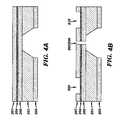
- FIG. 4Aillustrates a schematic of the integration of a tunneling junction with a nanopore in accordance with an exemplary embodiment.
- FIG. 4Billustrates a schematic continuing integration of a tunneling junction with a nanopore in accordance with an exemplary embodiment.
- FIG. 4Cillustrates a schematic continuing the integration of a tunneling junction with a nanopore in accordance with an exemplary embodiment.
- FIG. 5illustrates examples of molecules for self-assembly inside nanopores in accordance with an exemplary embodiment.
- FIG. 6illustrates a computer utilized according to exemplary embodiments.
- FIG. 7illustrates a flow chart according to an exemplary embodiment.
- Exemplary embodimentsprovide an approach to make a nanometer size tunneling junction by focus electron beam cutting, and then to fine tune the junction size, by expanded electron beam techniques. Exemplary embodiments also include the integration of such tunneling junction with a nanopore for the purpose of DNA sequencing in a nanodevice.
- nanoporesas sensors for rapid analysis of biomolecules such as DNA, ribonucleic acid (RNA), protein, etc.
- One issue in nanopore DNA sequencingis electrically differencing individual DNA bases by leveraging this nanopore platform.
- an approachwhich uses a focused electron beam (e.g., utilizing a beam size as small as 0.4 nm) to cut a thin metal layer (shown as cut line 105 in FIG. 1A ) to form the tunneling junction.
- a focused electron beame.g., utilizing a beam size as small as 0.4 nm
- material migrationcan occur, and the material migration can be used to fine tune the gap size of the tunneling junction.
- the thin metal layeris on a free-standing membrane, one can also make the nanopore (shown as nanopore 206 , 208 in FIGS. 2B-2I ) through the top of the membrane at the gap to create the tunneling junction right at the entrance, at the inner surface, and/or the exit of the nanopore for DNA sequencing purposes via the tunneling current.
- FIGS. 1A-1Cillustrate a schematic of a process to make a tunneling junction by focused electron beam cutting and to fine tune the junction size by expanded electron beam according to an exemplary embodiment.
- FIGS. 1A-1Care top views of the schematic.
- a substrate 101can be any electrically insulating substrate
- layer 102can be any electrically conductive layer such as a metal on top of the substrate 101 .
- Voltageis applied by voltage source 103 between two ends of the conductive layer 102 and current is monitored through the ammeter 104 .
- a focused electron beamcould be as small as 0.4 nm, and the focused electron beam performs line scanning shown as line 105 at the center location of conductive layer 102 (e.g., in a vacuum).
- One skilled in the artunderstands electron beam lithography (e-beam lithography), and understands the practice of scanning a beam of electrons in a patterned fashion across a surface.
- the high energy, high density electron beamcan sputter/etch material on its way into the vacuum gradually.
- the current measured by its corresponding ammeter 104serves as a feedback that the current through ammeter 104 will drop down to zero (0) once the conductive layer 102 is cut into two halves by the electron beam, as shown in FIG. 1B .
- FIG. 1Bshows a left half and right half of the conductive layer 102 . In this way, one can create a tunneling junction 106 without damaging the underneath substrate 101 .
- the tunneling junction 106which is a nanosize gap between two electrically conductive parts corresponds to the line 105 previously shown in FIG. 1A .
- the (metal) material in the conductive layer 102can migrate and the gap size of the tunneling junction 106 can be tuned; that is the tunneling junction 106 can be reduced or increased in size to be the tunneling junction 108 shown in FIG. 1C .
- a low intensity electron beamcan be used to bombard the conductive layer 102 at the tunneling junction (gap) 108 ( 106 in FIG. 1B ); this will cause the conductive layer 102 material to get softer and flow under surface tension.
- the low intensity electron beamcan be utilized to cause the conductive layer 102 material to flow such that the tunneling junction (gap) 108 is widened and/or flow such that the tunneling junction (gap) 108 is narrowed.
- tunneling junction (gap) 106material migration has caused the tunneling junction (gap) 106 to narrow. If the substrate 101 is a thin membrane, the whole tuning process can be monitored under a transmission electron microscope in real-time. Thus, one can acquire (tune) the exact size of the tunneling junction (gap) 108 by turning off the electron beam at the right moment. After fine tuning the tunneling junction 106 , the tunneling junction 106 is now represented as the finely tuned tunneling junction (gap) 108 in FIG. 1C .
- FIGS. 2A-2Fillustrate a schematic of the integration of the tunneling junction 108 with a nanopore in accordance with an exemplary embodiment.
- FIGS. 2A , 2 B, 2 D, and 2 Eare a cross-sectional view of the schematic
- FIGS. 2C and 2Fare top views of the schematic.
- the substrate 201can be any substrate, such as Si (silicon).
- Layers 202 and 203are electrically insulating films, such as Si 3 N 4 (compound of silicon and nitrogen).
- the insulating layer 203serves as an etching mask for etching thorough the substrate 201 via either dry or wet etching, and the etching stops on insulating layer 202 .
- Conductive layer 204(corresponding to conductive layer 102 in FIG. 1 ) is an electrically conductive layer, and tunneling junction 205 (corresponding to tunneling junction/gap 108 in FIG. 1 ) is the tunneling junction made in the free-standing membrane part of conductive layer 204 using the method described in FIG. 1 .
- the tunneling junction 205will be visible under a transmission electron microscope, and a nanometer size pore (nanopore) 206 can be made through the tunneling junction 205 and the underneath insulating layer 202 , as shown in FIG. 2B . In this way, the tunneling junction 205 is integrated with the nanopore 206 .
- the nanopore 206is a hole through the insulating layer 202 while the tunneling junction 205 is a gap in the conductive layer (metal) 204 .
- FIG. 2Cshows a top view of the schematic in FIG. 2B .
- the tunneling junction 205(corresponding to tunneling junction/gap 108 in FIG. 1 ) is only between the conductive layer (metal) 204 (corresponding to conductive layer 102 ), and the tunneling junction 205 splits the conductive layer 204 into a left half and a right half.
- the nanopore 206is formed through the tunneling junction 205 and goes through the substrate 201 .
- an insulating (cap) layer 207(also called the passivation layer which may be a layer of oxide and/or silicon nitride) is deposited on the conductive layer 204 , as shown in FIG. 2D (e.g., right after the tunneling junction 205 is made).
- the tunneling junction 205will be visible under a transmission electron microscope and a nanometer size pore (nanopore) 208 can be made through the tunneling junction 205 and the underneath insulating layer 202 , as shown in FIG. 2E . In this way, the tunneling junction 205 is embedded in the nanopore 208 .
- the nanopore 206may now be considered part of the nanopore 208 .
- Via windows 209 and 210are opened through the insulating layer 207 down to the conductive layer 204 , for electrically accessing the two sides of the tunneling junction 205 .
- the windows 209 and 210will be used as electrodes/connections for connecting, e.g., a wire to the left and right halves of the conductive layer 204 .
- FIG. 2Fillustrates the top view of FIG. 2E .
- the conductive layer 204(shown as an outline with a dotted line) is buried underneath the insulation (passivation) layer 207 with windows 209 and 210 of the conductive layer 204 exposed.
- the nanopore 208goes through the insulating layer 202 and the insulation (passivation) layer 207 .
- FIGS. 4A , 4 B, and 4 Cillustrate a variation of FIGS. 2A-2F in which the nanopore 208 and tunneling junction are made in the same electron beam cutting process and have the same shape in accordance with an exemplary embodiment.
- An insulating (cap) layer 207also called the passivation layer which may be a layer of oxide and/or silicon nitride
- a focused electron beamis used to cut through all layers 207 , 204 , and 202 at the freestanding membrane part and to cut conductive layer 204 into two halves, as shown in FIG. 4B . In this way, the tunneling junction 205 and the nanopore 208 have exactly the same shape.
- Via windows 209 and 210are opened through the insulating layer 207 down to the conductive layer 204 , for electrically accessing the two sides of the tunneling junction 205 .
- the windows 209 and 210will be used as electrodes/connections for connecting, e.g., a wire to the left and right halves of the conductive layer 204 .
- FIG. 4Cillustrates the top view of FIG. 4B .
- the conductive layer 204(shown as a dotted line) is buried underneath the insulating (passivation) layer 207 with windows 209 and 210 of the conductive layer 204 exposed.
- the nanopore 208goes through the insulating layer 202 and the insulating (passivation) layer 207 .
- FIGS. 3A and 3Billustrate a schematic (system) of a tunneling junction (e.g., tunneling junction 106 , 108 , and 205 ) and nanopore device 300 for DNA sequencing according to an exemplary embodiment.
- FIGS. 3A and 3Bshow a cross-sectional view of the tunneling junction and nanopore device 300 .
- elements 301 - 310are the same as elements 201 - 210 respectively.
- FIG. 3Bincludes an organic coating as discussed herein.
- the tunneling junction and nanopore device 300partitions two reservoirs 311 and 312 .
- Electrically conductive solution 313fills the two reservoirs 311 and 312 as well as the nanopore 308 .
- a negatively charged DNA 314(with each base illustrated as base 315 ) can be driven into the nanopore 308 by a voltage of the voltage source 318 applied between the two reservoirs 311 and 312 via two electrodes 316 and 317 , respectively.
- Voltage of the voltage source 319is applied between the two sides (at left window 309 and right window 310 ) of the tunneling junction 305 , and a baseline tunneling current is monitored at ammeter 320 .
- the baseline tunneling currentmay be stored in memory 15 of a computer 600 (shown in FIG. 6 ) for further use as discussed herein.
- a computer 600shown in FIG. 6
- each of the DNA bases 315can be indentified by its respective tunneling current signal at the ammeter 320 .
- voltage source 318is turned on to drive the DNA 314 into the tunneling junction 305 which is the gap separating the conductive layer 304 into two halves.
- voltage source 319is turned on (while voltage source 318 is turned off) to measure the tunneling current of the base 315 a .
- the ammeter 320may be implemented by and/or integrated in the computer 600 (test equipment) for measuring the baseline tunneling current and tunneling current generated by the DNA base 315 a .
- a software application 605 of the computer 600is configured to measure, display, plot/graph, analyze, and/or record the measured tunneling current for each DNA base 315 that is tested.
- the software application 605(and/or a user utilizing the software application 605 ) can compare the baseline tunneling current measured with no DNA base 315 in the tunneling junction 305 to the tunneling current corresponding to each DNA base 315 (at a time) that is measured in tunneling junction 305 .
- the tunneling current (signal) for the DNA base 315 ais compared against the baseline tunneling current by the software application 605 (or a user utilizing the software application 605 ).
- the tunneling current (signature) for the DNA base 315 amay have particular characteristics that are different from the baseline tunneling current measured by the ammeter 320 , and the tunneling current (signatures) for the DNA base 315 a can be utilized to identify and/or differentiate the DNA base 315 a from other DNA bases 315 on the DNA 314 .
- the measured tunneling current signature for DNA base 315 amay have a positive pulse, a negative pulse, a higher or lower current (magnitude), an inverse relationship, a rising or falling plot, a particular frequency, and/or any other difference from the baseline tunneling current that can be determined by the software application 605 (and/or a user viewing the display 45 of the two different plots).
- This unique tunneling current signaturecan be utilized (by the software application 605 ) to distinguish the DNA base 315 a from other DNA bases 315 .
- the tunneling current measured at ammeter 320 between electrode layersdoes not require any electrical wiring between the left and right parts (which will be shown as electrodes 304 a and 304 b in FIG.
- the conductive (electrode) layers 304 as electronssimply move from one electrode to the other in a quantum mechanical way.
- DNA base 315 ais close (e.g., within the distance of the wavelength of an electron) to the tunneling junction 305 , the tunneling path of the electron will be rerouted to tunnel from the left part of the conductive (electrode) layer 304 to the DNA base 315 a and then to the right part of the conductive (electrode) layer 304 .
- the tunneling current (electrons) through the DNA base 315 awill create a current signature (such as an increase of tunneling current, typically in the order of tens of pA (picoamperes)) added onto the baseline tunneling current trace.
- the tunneling current across DNA basesis dependent on the electronic and chemical structure of the DNA bases; thus, a different DNA base will generate a different tunneling current signature. If the difference between the tunneling current signatures of different bases is small or stochastic, repeating measurements on the same DNA base can be done; a histogram of the amplitudes of the tunneling current signatures can be fit and the statistical data will provide enough resolution to differentiate DNA bases.
- FIG. 3Butilizes the approach discussed for FIG. 3A except that the conductive layer 304 is coated with organic coating 325 a and 325 b , which can form transient bonds 321 a and 321 b (such as a hydrogen bond (i.e., transient bonds 321 ) with the DNA base 315 ).
- these transient bonds 321 formed by the organic coating 325 a and 325 bwill fix the orientation of the DNA base 315 and the relative distance of the DNA base 315 to the conductive layer 304 , for improving the tunneling current signal measured by ammeter 320 and for better identifying DNA bases 315 .
- the organic coating 325 a and 325 b and/or transient bonds 321 a and 321 bare electrically conductive, they will help to shrink the tunneling gap size and enhance the tunneling current signatures too. Also, the transient bonds 321 a and 321 b by the organic coating 325 a and 325 b hold the DNA 314 in place against thermal motion when measuring the tunneling current of the base 315 . The forces of thermal motion may cause the DNA 314 to move, but the transient bonds 321 a and 321 b fix the base 315 in the tunneling junction 305 against the DNA movement caused by thermal motion.
- the organic coating 325 a and 325 bconsists of bifunctional small molecules which at one end form covalent bonds with conductive layer 304 , and at the other end (of the organic coating 325 a/b ) which is exposed in the nanopore 308 , the organic coating 325 a and 325 b consists of functionalities which can form strong hydrogen bonds with DNA and/or can protonate nucleotides to form acid base interactions.
- the conductive layer 304is made of metals such as gold, palladium, platinum etc.
- the first functionality which bonds to the conductive layer 304can be chosen as thiols, isocyanides, and/or diazonium salts.
- the covalent bonding functionalityis chosen from phosphonic acid, hydroxamic acid, and/or resorcinol functionality.
- the small bifunctional moleculesare designed in such a way that any charge formation due to interaction with DNA can easily be transferred to the conductive layer 304 and therefore a pi-conjugated moiety (e.g., benzene, diphenyl, etc.) are sandwiched between two functionalities.
- the second functionalityis a group which can form a strong hydrogen bond with DNA. Examples of such groups include but are not limited to alcohols, carboxylic acids, carboxamides, sulfonamides, and/or sulfonic acids.
- FIG. 5illustrates examples of molecules for self-assembly inside nanopores according to exemplary embodiments.
- the moleculesmay be utilized as the organic coating 325 a and 325 b.
- the voltage source 318is applied to move the DNA 314 into the nanopore 308 .
- voltage of the voltage source 319is applied (and the voltage source 318 is turned off)
- currentflows through left electrode 304 a , into the organic coating 325 a , into the transient bond 321 a (which acts as or can be thought of as a wire), into the DNA base 315 a (producing the tunneling current), out through the transient bond 321 b , out through the organic coating 325 b , out through the right electrode 304 b , and into the ammeter 320 to measure the tunneling current of the DNA base 315 a .
- the ammeter 320may be integrated with the computer 600 , and the computer 600 can display on display 45 the tunneling current of the DNA base 315 a versus the baseline tunneling current measured when no base 315 is in the tunneling junction 305 .
- FIG. 7illustrates a method 700 according to exemplary embodiments, and reference can be made to FIGS. 1 , 2 , and 3 .
- a tunneling junction 108 , 205 , 305is made by electron beam sculpting (cutting or size-tuning).
- the tunneling junction 108 , 205 , 305can be widened by causing the material (metal) of the conductive layer 102 , 204 , 304 to migrate away from the tunneling junction gap, thus making the gap wider; similarly, using a low intensity electron beam spread across area 107 in FIG. 1 , the tunneling junction 108 , 205 , 305 can be narrowed to cause the material of the conductive layer 102 , 204 , 304 to flow toward (into) the tunneling junction gap thus make the gap smaller.
- the tunneling junction 108 , 205is integrated with a nanopore 208 as shown in FIGS. 2B-2F .
- the integrated (combined) tunneling junction 205 and nanopore 208form a hole through multiple layers 207 , 204 , and 202 as shown in FIG. 2E .
- the distinction between the tunneling junction 205 and the nanopore 208can be seen in FIG. 2F .
- This distinctionis carried through to the tunneling junction 305 shown in FIG. 3 in which the tunneling junction 305 is the gap between the conductive layer 304 (i.e., separating the conductive layer 304 into two halves) but not layers 307 , 302 , 301 , and 303 .
- the tunneling junction 108 , 205is formed prior to forming the nanopore 208 (and/or nanopore 206 ).
- the nanopore 208partitions two conductive ionic buffer reservoirs 312 and 313 , and the DNA 314 is electrically loaded into the nanopore 308 and the tunneling junction 305 .
- the tunneling junction 305is between the left half 304 a and right half 304 b of the conductive layer 304 .
- the left and right halves 304 a and 304 bserve as electrodes for accessing the tunneling junction 305 (and the base 315 therein) by the voltage source 319 to measure the tunneling current with ammeter 320 .
- the DNA bases 315are differentiated using the tunneling current of each individual base 315 (measured by ammeter 320 ) with and/or without organic coating 325 a and 325 b on the inside surface of the tunneling junction 305 .
- the computer 600can measure, analyze, differentiate, display, and record/store (in memory 15 ) the different tunneling currents measured for the different bases 315 of the DNA 314 .
- the tunneling current measurements of the bases 315 with the organic coating 325 a and 325 b causing the transient bonds 321 a and 321 bwould be different from the tunneling currents measurements of the same bases 315 without the organic coating 325 a and 325 b and without the transient bonds.
- the tunneling current measured for base 315 a with the organic coating 325 a and 325 bmay have a greater magnitude than without the organic coating 325 a and 325 b.
- FIG. 6illustrates a block diagram of the computer 600 having various software and hardware elements for implementing exemplary embodiments.
- the computer 600may be utilized in conjunction with any elements discussed herein.
- the diagramdepicts the computer 600 which may be any type of computing device and/or test equipment (including ammeters, voltage sources, connectors, etc.).
- the computer 600may include and/or be coupled to memory 15 , a communication interface 40 , display 45 , user interfaces 50 , processors 60 , and software 605 .
- the communication interface 40comprises hardware and software for communicating over a network and connecting (via cables, plugs, wires, electrodes, etc.) to the nanodevices discussed herein.
- the communication interface 40comprises hardware and software for communicating with, operatively connecting to, reading, and controlling voltage sources, ammeters, tunneling currents, etc., as discussed herein.
- the user interfaces 50may include, e.g., a track ball, mouse, pointing device, keyboard, touch screen, etc, for interacting with the computer 600 , such as inputting information, making selections, independently controlling different voltages sources, and/or displaying, viewing and recording tunneling current signatures for each base, etc.
- the computer 600includes memory 15 which may be a computer readable storage medium.
- One or more applicationssuch as the software application 605 (e.g., a software tool) may reside on or be coupled to the memory 15 , and the software application 605 comprises logic and software components to operate and function in accordance with exemplary embodiments in the form of computer executable instructions.
- the software application 605may include a graphical user interface (GUI) which the user can view and interact with according to exemplary embodiments.
- GUIgraphical user interface
- aspects of the present inventionmay be embodied as a system, method or computer program product. Accordingly, aspects of the present invention may take the form of an entirely hardware embodiment, an entirely software embodiment (including firmware, resident software, micro-code, etc.) or an embodiment combining software and hardware aspects that may all generally be referred to herein as a “circuit,” “module” or “system.” Furthermore, aspects of the present invention may take the form of a computer program product embodied in one or more computer readable medium(s) having computer readable program code embodied thereon.
- the computer readable mediummay be a computer readable signal medium or a computer readable storage medium.
- a computer readable storage mediummay be, for example, but not limited to, an electronic, magnetic, optical, electromagnetic, infrared, or semiconductor system, apparatus, or device, or any suitable combination of the foregoing.
- a computer readable storage mediummay be any tangible medium that can contain, or store a program for use by or in connection with an instruction execution system, apparatus, or device.
- a computer readable signal mediummay include a propagated data signal with computer readable program code embodied therein, for example, in baseband or as part of a carrier wave. Such a propagated signal may take any of a variety of forms, including, but not limited to, electro-magnetic, optical, or any suitable combination thereof.
- a computer readable signal mediummay be any computer readable medium that is not a computer readable storage medium and that can communicate, propagate, or transport a program for use by or in connection with an instruction execution system, apparatus, or device.
- Program code embodied on a computer readable mediummay be transmitted using any appropriate medium, including but not limited to wireless, wireline, optical fiber cable, RF, etc., or any suitable combination of the foregoing.
- Computer program code for carrying out operations for aspects of the present inventionmay be written in any combination of one or more programming languages, including an object oriented programming language such as Java, Smalltalk, C++ or the like and conventional procedural programming languages, such as the “C” programming language or similar programming languages.
- the program codemay execute entirely on the user's computer, partly on the user's computer, as a stand-alone software package, partly on the user's computer and partly on a remote computer or entirely on the remote computer or server.
- the remote computermay be connected to the user's computer through any type of network, including a local area network (LAN) or a wide area network (WAN), or the connection may be made to an external computer (for example, through the Internet using an Internet Service Provider).
- LANlocal area network
- WANwide area network
- Internet Service Providerfor example, AT&T, MCI, Sprint, EarthLink, MSN, GTE, etc.
- These computer program instructionsmay also be stored in a computer readable medium that can direct a computer, other programmable data processing apparatus, or other devices to function in a particular manner, such that the instructions stored in the computer readable medium produce an article of manufacture including instructions which implement the function/act specified in the flowchart and/or block diagram block or blocks.
- the computer program instructionsmay also be loaded onto a computer, other programmable data processing apparatus, or other devices to cause a series of operational steps to be performed on the computer, other programmable apparatus or other devices to produce a computer implemented process such that the instructions which execute on the computer or other programmable apparatus provide processes for implementing the functions/acts specified in the flowchart and/or block diagram block or blocks.
- each block in the flowchart or block diagramsmay represent a module, segment, or portion of code, which comprises one or more executable instructions for implementing the specified logical function(s).
- the functions noted in the blockmay occur out of the order noted in the figures. For example, two blocks shown in succession may, in fact, be executed substantially concurrently, or the blocks may sometimes be executed in the reverse order, depending upon the functionality involved.
Landscapes
- Engineering & Computer Science (AREA)
- Health & Medical Sciences (AREA)
- Life Sciences & Earth Sciences (AREA)
- Biomedical Technology (AREA)
- Chemical & Material Sciences (AREA)
- Physics & Mathematics (AREA)
- Molecular Biology (AREA)
- Medicinal Chemistry (AREA)
- Biophysics (AREA)
- Hematology (AREA)
- Nanotechnology (AREA)
- Urology & Nephrology (AREA)
- Food Science & Technology (AREA)
- Spectroscopy & Molecular Physics (AREA)
- Analytical Chemistry (AREA)
- Biochemistry (AREA)
- General Health & Medical Sciences (AREA)
- General Physics & Mathematics (AREA)
- Immunology (AREA)
- Pathology (AREA)
- Investigating Or Analyzing Materials By The Use Of Electric Means (AREA)
- Apparatus Associated With Microorganisms And Enzymes (AREA)
Abstract
Description
Claims (1)
Priority Applications (2)
| Application Number | Priority Date | Filing Date | Title |
|---|---|---|---|
| US13/359,729US8852407B2 (en) | 2011-01-28 | 2012-01-27 | Electron beam sculpting of tunneling junction for nanopore DNA sequencing |
| US13/606,815US8858764B2 (en) | 2011-01-28 | 2012-09-07 | Electron beam sculpting of tunneling junction for nanopore DNA sequencing |
Applications Claiming Priority (2)
| Application Number | Priority Date | Filing Date | Title |
|---|---|---|---|
| US201161437102P | 2011-01-28 | 2011-01-28 | |
| US13/359,729US8852407B2 (en) | 2011-01-28 | 2012-01-27 | Electron beam sculpting of tunneling junction for nanopore DNA sequencing |
Related Child Applications (1)
| Application Number | Title | Priority Date | Filing Date |
|---|---|---|---|
| US13/606,815ContinuationUS8858764B2 (en) | 2011-01-28 | 2012-09-07 | Electron beam sculpting of tunneling junction for nanopore DNA sequencing |
Publications (2)
| Publication Number | Publication Date |
|---|---|
| US20120193236A1 US20120193236A1 (en) | 2012-08-02 |
| US8852407B2true US8852407B2 (en) | 2014-10-07 |
Family
ID=46576444
Family Applications (2)
| Application Number | Title | Priority Date | Filing Date |
|---|---|---|---|
| US13/359,729Active2032-04-27US8852407B2 (en) | 2011-01-28 | 2012-01-27 | Electron beam sculpting of tunneling junction for nanopore DNA sequencing |
| US13/606,815Expired - Fee RelatedUS8858764B2 (en) | 2011-01-28 | 2012-09-07 | Electron beam sculpting of tunneling junction for nanopore DNA sequencing |
Family Applications After (1)
| Application Number | Title | Priority Date | Filing Date |
|---|---|---|---|
| US13/606,815Expired - Fee RelatedUS8858764B2 (en) | 2011-01-28 | 2012-09-07 | Electron beam sculpting of tunneling junction for nanopore DNA sequencing |
Country Status (1)
| Country | Link |
|---|---|
| US (2) | US8852407B2 (en) |
Cited By (4)
| Publication number | Priority date | Publication date | Assignee | Title |
|---|---|---|---|---|
| US20160203258A1 (en)* | 2015-01-14 | 2016-07-14 | International Business Machines Corporation | Dna sequencing using mosfet transistors |
| US9513277B2 (en) | 2011-01-28 | 2016-12-06 | International Business Machines Corporation | DNA sequencing using multiple metal layer structure with different organic coatings forming different transient bondings to DNA |
| US9768104B1 (en) | 2016-08-19 | 2017-09-19 | International Business Machines Corporation | Method and structure to fabricate a nanoporous membrane |
| US10029915B2 (en) | 2012-04-04 | 2018-07-24 | International Business Machines Corporation | Functionally switchable self-assembled coating compound for controlling translocation of molecule through nanopores |
Families Citing this family (19)
| Publication number | Priority date | Publication date | Assignee | Title |
|---|---|---|---|---|
| US8852407B2 (en) | 2011-01-28 | 2014-10-07 | International Business Machines Corporation | Electron beam sculpting of tunneling junction for nanopore DNA sequencing |
| US20120193231A1 (en)* | 2011-01-28 | 2012-08-02 | International Business Machines Corporation | Dna sequencing using multiple metal layer structure with organic coatings forming transient bonding to dna bases |
| JP5670278B2 (en)* | 2011-08-09 | 2015-02-18 | 株式会社日立ハイテクノロジーズ | Nanopore analyzer |
| WO2013192178A1 (en)* | 2012-06-18 | 2013-12-27 | Electronic Biosciences Inc. | Cell-free assay device and methods of use |
| KR20140028602A (en)* | 2012-08-29 | 2014-03-10 | 삼성전자주식회사 | Nano sensor including grapheme and method of manufacturing the same |
| DE102012217228A1 (en)* | 2012-09-25 | 2014-03-27 | Siemens Aktiengesellschaft | Manufacturing method for a nanopore-containing part and corresponding nanopore-containing part |
| DE102012217603A1 (en)* | 2012-09-27 | 2014-03-27 | Siemens Aktiengesellschaft | Arrangement for nucleic acid sequencing by tunneling current analysis |
| US9046511B2 (en) | 2013-04-18 | 2015-06-02 | International Business Machines Corporation | Fabrication of tunneling junction for nanopore DNA sequencing |
| US8890121B1 (en)* | 2013-05-06 | 2014-11-18 | International Business Machines Corporation | Integrated nanowire/nanosheet nanogap and nanopore for DNA and RNA sequencing |
| US9188578B2 (en) | 2013-06-19 | 2015-11-17 | Globalfoundries Inc. | Nanogap device with capped nanowire structures |
| US9182369B2 (en) | 2013-06-19 | 2015-11-10 | Globalfoundries Inc. | Manufacturable sub-3 nanometer palladium gap devices for fixed electrode tunneling recognition |
| CN103820311B (en)* | 2014-02-26 | 2016-02-24 | 清华大学 | For nanopore device and using method, the making method of single-molecule sequencing |
| US10612084B2 (en)* | 2014-04-08 | 2020-04-07 | International Business Machines Corporation | Reduction of entropic barrier of polyelectrolyte molecules in a nanopore device with agarose gel |
| DE102016200781A1 (en)* | 2016-01-21 | 2017-07-27 | Robert Bosch Gmbh | Method for producing a pore device for analysis of molecules, microfluidic system for analyzing molecules, control device and method for analyzing molecules |
| EP3810803B1 (en)* | 2018-06-21 | 2024-01-24 | F. Hoffmann-La Roche AG | Tunneling junctions for sequencing |
| US11493499B1 (en) | 2018-10-30 | 2022-11-08 | Seagate Technology Llc | Event timing detection for DNA sequencing |
| US12408558B2 (en) | 2020-07-08 | 2025-09-02 | Arizona Board Of Regents On Behalf Of Arizona State University | Method for constructing magnetic tunneling junction devices and use of device for spin-dependent transport characterization |
| IL305947A (en) | 2021-03-16 | 2023-11-01 | Univ Arizona State | High density and multiplexed nanopore devices with transverse tunneling junction for biomolecule detection and sequencing |
| US20240027395A1 (en)* | 2022-07-21 | 2024-01-25 | Acorn Genetics Inc. | Graphene nanoribbon with nanopore-based signal detection and genetic sequencing technology |
Citations (66)
| Publication number | Priority date | Publication date | Assignee | Title |
|---|---|---|---|---|
| US4576829A (en) | 1984-12-28 | 1986-03-18 | Rca Corporation | Low temperature growth of silicon dioxide on silicon |
| US4692992A (en) | 1986-06-25 | 1987-09-15 | Rca Corporation | Method of forming isolation regions in a semiconductor device |
| EP0261592A1 (en) | 1986-09-17 | 1988-03-30 | Otsuka Pharmaceutical Co., Ltd. | Gene coding for human colony-stimulating factors |
| US5671086A (en) | 1995-04-18 | 1997-09-23 | The Regents, University Of California | Method and apparatus for accurately manipulating an object during microelectrophoresis |
| US6180490B1 (en) | 1999-05-25 | 2001-01-30 | Chartered Semiconductor Manufacturing Ltd. | Method of filling shallow trenches |
| US6217872B1 (en) | 1990-06-25 | 2001-04-17 | The Research Foundation For Microbial Diseases Of Osaka University | Non-A, non-B hepatitis virus genomic cDNA and antigen polypeptide |
| WO2001081908A1 (en) | 2000-04-24 | 2001-11-01 | Eagle Research & Development, Llc | Field effect transistor device for ultra-fast nucleic acid sequencing |
| US6582926B1 (en) | 1999-03-19 | 2003-06-24 | Duke University | Methods of using bioelastomers |
| US6621191B1 (en) | 1999-05-13 | 2003-09-16 | Matsushita Electric Industrial Co., Inc. | Structure containing organic molecular layer and use thereof |
| US6627067B1 (en) | 1999-06-22 | 2003-09-30 | President And Fellows Of Harvard College | Molecular and atomic scale evaluation of biopolymers |
| US6727174B1 (en) | 1998-03-10 | 2004-04-27 | International Business Machines Corporation | Method for fabricating a dual-diameter electrical conductor |
| EP1441213A1 (en) | 2003-01-27 | 2004-07-28 | Agilent Technologies Inc. (a Delaware Corporation) | Apparatus and method for biopolymer identification during translocation through a nanopore |
| US6777260B1 (en) | 2003-08-14 | 2004-08-17 | Silicon Storage Technology, Inc. | Method of making sub-lithographic sized contact holes |
| US20040229386A1 (en)* | 1999-06-22 | 2004-11-18 | President And Fellows Of Harvard College | Controlled fabrication of gaps in electrically conducting structures |
| EP1486775A1 (en) | 2003-06-12 | 2004-12-15 | Agilent Technologies, Inc. (a Delaware Corporation) | Nanopore with resonant tunneling electrodes |
| US20050019784A1 (en) | 2002-05-20 | 2005-01-27 | Xing Su | Method and apparatus for nucleic acid sequencing and identification |
| US20050026238A1 (en) | 2003-07-28 | 2005-02-03 | Berndt Klaus W. | System and method for detecting particles |
| US20050101100A1 (en) | 2003-11-06 | 2005-05-12 | General Electric Company | Integrated devices with optical and electrical isolation and method for making |
| US20050110990A1 (en) | 2003-10-17 | 2005-05-26 | Tae-Woong Koo | Method and device for detecting small numbers of molecules using surface-enhanced coherent anti-Stokes Raman spectroscopy |
| US20050158763A1 (en) | 2003-12-19 | 2005-07-21 | Albena Ivanisevic | Aligned long DNA molecules on templates and methods for preparing |
| US6962849B1 (en) | 2003-12-05 | 2005-11-08 | Advanced Micro Devices, Inc. | Hard mask spacer for sublithographic bitline |
| US20060105553A1 (en) | 2004-11-12 | 2006-05-18 | Uwe Wellhausen | Reversible oxidation protection of microcomponents |
| US20060154399A1 (en) | 2000-04-24 | 2006-07-13 | Sauer Jon R | Ultra-fast nucleic acid sequencing device and a method for making and using the same |
| US20060169588A1 (en) | 2005-02-02 | 2006-08-03 | Jacobson Stephen C | Microfluidic device and methods for focusing fluid streams using electroosmotically induced pressures |
| US20060180469A1 (en) | 2005-01-25 | 2006-08-17 | Jongyoon Han | Electrokinetic concentration device and methods of use thereof |
| US20060246497A1 (en) | 2005-04-27 | 2006-11-02 | Jung-Tang Huang | Ultra-rapid DNA sequencing method with nano-transistors array based devices |
| WO2006122317A2 (en) | 2005-05-11 | 2006-11-16 | The Regents Of The University Of California | Nanofabrication processes and devices for the controlled assembly of functionalized nanostructures |
| US20070020146A1 (en) | 2005-06-29 | 2007-01-25 | Young James E | Nanopore structure and method using an insulating substrate |
| US20070042366A1 (en) | 2003-02-28 | 2007-02-22 | Brown University | Nanopores, methods for using same, methods for making same and methods for characterizing biomolecules using same |
| US20070048745A1 (en) | 2005-08-30 | 2007-03-01 | Joyce Timothy H | Systems and methods for partitioned nanopore analysis of polymers |
| WO2007084163A2 (en) | 2005-04-06 | 2007-07-26 | President And Fellows Of Harvard College | Molecular characterization with carbon nanotube control |
| US20070187694A1 (en) | 2006-02-16 | 2007-08-16 | Pfeiffer Loren N | Devices including graphene layers epitaxially grown on single crystal substrates |
| US20070190542A1 (en) | 2005-10-03 | 2007-08-16 | Ling Xinsheng S | Hybridization assisted nanopore sequencing |
| US7282130B2 (en) | 2003-01-31 | 2007-10-16 | Agilent Technologies, Inc. | Apparatus and method for control of biopolymer translocation through a nanopore |
| US20080003571A1 (en) | 2005-02-01 | 2008-01-03 | Mckernan Kevin | Reagents, methods, and libraries for bead-based sequencing |
| US20080032290A1 (en) | 2006-08-03 | 2008-02-07 | Young James E | Nanopore flow cells |
| US7347921B2 (en) | 2003-07-17 | 2008-03-25 | Agilent Technologies, Inc. | Apparatus and method for threading a biopolymer through a nanopore |
| US7351648B2 (en) | 2006-01-19 | 2008-04-01 | International Business Machines Corporation | Methods for forming uniform lithographic features |
| US20080102504A1 (en) | 2004-03-23 | 2008-05-01 | Mark Akeson | Methods and apparatus for characterizing polynucleotides |
| WO2008051308A2 (en) | 2006-05-05 | 2008-05-02 | University Of Utah Research Foundation | A nanopore particle analyzer, method of preparation and use thereof |
| US20080187915A1 (en) | 2007-02-02 | 2008-08-07 | Stanislav Polonsky | Systems and Methods for Controlling the Position of a Charged Polymer Inside a Nanopore |
| WO2008132643A1 (en) | 2007-04-25 | 2008-11-06 | Nxp B.V. | Apparatus and method for molecule detection using nanopores |
| WO2009020682A2 (en)* | 2007-05-08 | 2009-02-12 | The Trustees Of Boston University | Chemical functionalization of solid-state nanopores and nanopore arrays and applications thereof |
| WO2009032756A2 (en) | 2007-08-28 | 2009-03-12 | University Of Florida Research Foundation, Inc. | Bio-sensor using gated electrokinetic transport |
| US20090136958A1 (en) | 2007-10-02 | 2009-05-28 | President And Fellows Of Harvard College | Capture, recapture, and trapping of molecules with a nanopore |
| US7540717B2 (en) | 2005-06-03 | 2009-06-02 | The Hong Kong University Of Science And Technology | Membrane nanopumps based on porous alumina thin films, membranes therefor and a method of fabricating such membranes |
| US7553730B2 (en) | 2006-07-14 | 2009-06-30 | Agilent Technologies, Inc. | Methods of fabrication employing nanoscale mandrels |
| US7560141B1 (en) | 2008-11-11 | 2009-07-14 | International Business Machines Corporation | Method of positioning patterns from block copolymer self-assembly |
| US20090188794A1 (en) | 2008-01-25 | 2009-07-30 | Steve Simon | Device for Fluid Spreading and Transport |
| US20090222216A1 (en) | 2008-02-28 | 2009-09-03 | Electronic Bio Sciences, Llc | System and Method to Improve Accuracy of a Polymer |
| US20100084276A1 (en) | 2007-04-06 | 2010-04-08 | Stuart Lindsay | Devices and Methods for Target Molecule Characterization |
| US7846738B2 (en) | 2003-08-15 | 2010-12-07 | President And Fellows Of Harvard College | Study of polymer molecules and conformations with a nanopore |
| US20100327847A1 (en) | 2007-09-12 | 2010-12-30 | President And Fellows Of Harvard College | High-Resolution Molecular Sensor |
| US20100327255A1 (en) | 2009-06-29 | 2010-12-30 | International Business Machines Corporation | Nanofludic field effect transistor based on surface charge modulated nanochannel |
| US20100331194A1 (en) | 2009-04-10 | 2010-12-30 | Pacific Biosciences Of California, Inc. | Nanopore sequencing devices and methods |
| US20110052813A1 (en) | 2008-01-03 | 2011-03-03 | Peter Ho | Functionalised graphene oxide |
| US20110085759A1 (en) | 2008-03-28 | 2011-04-14 | Kitakyushu Found.For The Adv.Of Ind., Sci. & Tech. | Composite thin film, and atmosphere sensor and optical waveguide sensor each including the same |
| US20110220574A1 (en) | 2008-05-29 | 2011-09-15 | Olgica Bakajin | Membranes With Functionalized Carbon Nanotube Pores For Selective Transport |
| US20110236984A1 (en) | 2010-01-04 | 2011-09-29 | Life Technologies Corporation | Dna sequencing methods and detectors and systems for carrying out the same |
| US20110279125A1 (en) | 2010-05-17 | 2011-11-17 | International Business Machines Corporation | FET Nanopore Sensor |
| US20120146162A1 (en) | 2010-12-13 | 2012-06-14 | Samsung Electronics Co., Ltd. | Nanosensor and method of manufacturing the same |
| US20120193236A1 (en) | 2011-01-28 | 2012-08-02 | International Business Machines Corporation | Electron beam sculpting of tunneling junction for nanopore dna sequencing |
| US20120193235A1 (en) | 2011-01-28 | 2012-08-02 | International Business Machines Corporation | Dna motion control based on nanopore with organic coating forming transient bonding to dna |
| US20120193237A1 (en) | 2011-01-28 | 2012-08-02 | International Business Machines Corporation | Dna sequencing using multiple metal layer structure with different organic coatings forming different transient bondings to dna |
| US20130037410A1 (en) | 2010-11-16 | 2013-02-14 | Zhejiang University | Nanopore Sensor Comprising A Sub-Nanometer-Thick Layer |
| US20130203050A1 (en) | 2009-09-30 | 2013-08-08 | Quantapore, Inc. | Hybrid nanopore device with optical detection and methods of using same |
Family Cites Families (1)
| Publication number | Priority date | Publication date | Assignee | Title |
|---|---|---|---|---|
| FR2927169B1 (en)* | 2008-02-05 | 2013-01-11 | Commissariat Energie Atomique | METHOD FOR FUNCTIONALIZING THE SURFACE OF A PORE |
- 2012
- 2012-01-27USUS13/359,729patent/US8852407B2/enactiveActive
- 2012-09-07USUS13/606,815patent/US8858764B2/ennot_activeExpired - Fee Related
Patent Citations (74)
| Publication number | Priority date | Publication date | Assignee | Title |
|---|---|---|---|---|
| US4576829A (en) | 1984-12-28 | 1986-03-18 | Rca Corporation | Low temperature growth of silicon dioxide on silicon |
| US4692992A (en) | 1986-06-25 | 1987-09-15 | Rca Corporation | Method of forming isolation regions in a semiconductor device |
| EP0261592A1 (en) | 1986-09-17 | 1988-03-30 | Otsuka Pharmaceutical Co., Ltd. | Gene coding for human colony-stimulating factors |
| US6217872B1 (en) | 1990-06-25 | 2001-04-17 | The Research Foundation For Microbial Diseases Of Osaka University | Non-A, non-B hepatitis virus genomic cDNA and antigen polypeptide |
| US5671086A (en) | 1995-04-18 | 1997-09-23 | The Regents, University Of California | Method and apparatus for accurately manipulating an object during microelectrophoresis |
| US6727174B1 (en) | 1998-03-10 | 2004-04-27 | International Business Machines Corporation | Method for fabricating a dual-diameter electrical conductor |
| US6582926B1 (en) | 1999-03-19 | 2003-06-24 | Duke University | Methods of using bioelastomers |
| US6621191B1 (en) | 1999-05-13 | 2003-09-16 | Matsushita Electric Industrial Co., Inc. | Structure containing organic molecular layer and use thereof |
| US6180490B1 (en) | 1999-05-25 | 2001-01-30 | Chartered Semiconductor Manufacturing Ltd. | Method of filling shallow trenches |
| US6627067B1 (en) | 1999-06-22 | 2003-09-30 | President And Fellows Of Harvard College | Molecular and atomic scale evaluation of biopolymers |
| US20040229386A1 (en)* | 1999-06-22 | 2004-11-18 | President And Fellows Of Harvard College | Controlled fabrication of gaps in electrically conducting structures |
| US6413792B1 (en) | 2000-04-24 | 2002-07-02 | Eagle Research Development, Llc | Ultra-fast nucleic acid sequencing device and a method for making and using the same |
| US20060154399A1 (en) | 2000-04-24 | 2006-07-13 | Sauer Jon R | Ultra-fast nucleic acid sequencing device and a method for making and using the same |
| WO2001081908A1 (en) | 2000-04-24 | 2001-11-01 | Eagle Research & Development, Llc | Field effect transistor device for ultra-fast nucleic acid sequencing |
| US20080119366A1 (en) | 2000-04-24 | 2008-05-22 | Sauer Jon R | Ultra-Fast Nucleic Acid Sequencing Device and a Method for Making and Using the Same |
| US20050019784A1 (en) | 2002-05-20 | 2005-01-27 | Xing Su | Method and apparatus for nucleic acid sequencing and identification |
| EP1441213A1 (en) | 2003-01-27 | 2004-07-28 | Agilent Technologies Inc. (a Delaware Corporation) | Apparatus and method for biopolymer identification during translocation through a nanopore |
| US7282130B2 (en) | 2003-01-31 | 2007-10-16 | Agilent Technologies, Inc. | Apparatus and method for control of biopolymer translocation through a nanopore |
| US20070042366A1 (en) | 2003-02-28 | 2007-02-22 | Brown University | Nanopores, methods for using same, methods for making same and methods for characterizing biomolecules using same |
| US20070138132A1 (en) | 2003-06-12 | 2007-06-21 | Barth Phillip W | Nanopore with resonant tunneling electrodes |
| EP1486775A1 (en) | 2003-06-12 | 2004-12-15 | Agilent Technologies, Inc. (a Delaware Corporation) | Nanopore with resonant tunneling electrodes |
| US7347921B2 (en) | 2003-07-17 | 2008-03-25 | Agilent Technologies, Inc. | Apparatus and method for threading a biopolymer through a nanopore |
| US20050026238A1 (en) | 2003-07-28 | 2005-02-03 | Berndt Klaus W. | System and method for detecting particles |
| US6777260B1 (en) | 2003-08-14 | 2004-08-17 | Silicon Storage Technology, Inc. | Method of making sub-lithographic sized contact holes |
| US7846738B2 (en) | 2003-08-15 | 2010-12-07 | President And Fellows Of Harvard College | Study of polymer molecules and conformations with a nanopore |
| US20050110990A1 (en) | 2003-10-17 | 2005-05-26 | Tae-Woong Koo | Method and device for detecting small numbers of molecules using surface-enhanced coherent anti-Stokes Raman spectroscopy |
| US20050101100A1 (en) | 2003-11-06 | 2005-05-12 | General Electric Company | Integrated devices with optical and electrical isolation and method for making |
| US6962849B1 (en) | 2003-12-05 | 2005-11-08 | Advanced Micro Devices, Inc. | Hard mask spacer for sublithographic bitline |
| US20050158763A1 (en) | 2003-12-19 | 2005-07-21 | Albena Ivanisevic | Aligned long DNA molecules on templates and methods for preparing |
| US20080102504A1 (en) | 2004-03-23 | 2008-05-01 | Mark Akeson | Methods and apparatus for characterizing polynucleotides |
| US20060105553A1 (en) | 2004-11-12 | 2006-05-18 | Uwe Wellhausen | Reversible oxidation protection of microcomponents |
| US20060180469A1 (en) | 2005-01-25 | 2006-08-17 | Jongyoon Han | Electrokinetic concentration device and methods of use thereof |
| US20080003571A1 (en) | 2005-02-01 | 2008-01-03 | Mckernan Kevin | Reagents, methods, and libraries for bead-based sequencing |
| US20060169588A1 (en) | 2005-02-02 | 2006-08-03 | Jacobson Stephen C | Microfluidic device and methods for focusing fluid streams using electroosmotically induced pressures |
| WO2007084163A2 (en) | 2005-04-06 | 2007-07-26 | President And Fellows Of Harvard College | Molecular characterization with carbon nanotube control |
| US7468271B2 (en) | 2005-04-06 | 2008-12-23 | President And Fellows Of Harvard College | Molecular characterization with carbon nanotube control |
| US20080257859A1 (en) | 2005-04-06 | 2008-10-23 | President And Fellows Of Harvard College | Molecular characterization with carbon nanotube control |
| US20080171316A1 (en) | 2005-04-06 | 2008-07-17 | President And Fellows Of Harvard College | Molecular characterization with carbon nanotube control |
| US20060246497A1 (en) | 2005-04-27 | 2006-11-02 | Jung-Tang Huang | Ultra-rapid DNA sequencing method with nano-transistors array based devices |
| US20090221443A1 (en) | 2005-05-11 | 2009-09-03 | The Regents Of The University Of California | Nanofabrication processes and devices for the controlled assembly of functionalized nanostructures |
| WO2006122317A2 (en) | 2005-05-11 | 2006-11-16 | The Regents Of The University Of California | Nanofabrication processes and devices for the controlled assembly of functionalized nanostructures |
| US7540717B2 (en) | 2005-06-03 | 2009-06-02 | The Hong Kong University Of Science And Technology | Membrane nanopumps based on porous alumina thin films, membranes therefor and a method of fabricating such membranes |
| US20070020146A1 (en) | 2005-06-29 | 2007-01-25 | Young James E | Nanopore structure and method using an insulating substrate |
| US20070048745A1 (en) | 2005-08-30 | 2007-03-01 | Joyce Timothy H | Systems and methods for partitioned nanopore analysis of polymers |
| US20070190542A1 (en) | 2005-10-03 | 2007-08-16 | Ling Xinsheng S | Hybridization assisted nanopore sequencing |
| US7351648B2 (en) | 2006-01-19 | 2008-04-01 | International Business Machines Corporation | Methods for forming uniform lithographic features |
| US20070187694A1 (en) | 2006-02-16 | 2007-08-16 | Pfeiffer Loren N | Devices including graphene layers epitaxially grown on single crystal substrates |
| WO2008051308A2 (en) | 2006-05-05 | 2008-05-02 | University Of Utah Research Foundation | A nanopore particle analyzer, method of preparation and use thereof |
| US7553730B2 (en) | 2006-07-14 | 2009-06-30 | Agilent Technologies, Inc. | Methods of fabrication employing nanoscale mandrels |
| US20080032290A1 (en) | 2006-08-03 | 2008-02-07 | Young James E | Nanopore flow cells |
| US20080187915A1 (en) | 2007-02-02 | 2008-08-07 | Stanislav Polonsky | Systems and Methods for Controlling the Position of a Charged Polymer Inside a Nanopore |
| US20100025249A1 (en) | 2007-02-02 | 2010-02-04 | International Business Machines Corporation | Systems and Methods for Controlling the Position of a Charged Polymer Inside a Nanopore |
| US20100084276A1 (en) | 2007-04-06 | 2010-04-08 | Stuart Lindsay | Devices and Methods for Target Molecule Characterization |
| WO2008132643A1 (en) | 2007-04-25 | 2008-11-06 | Nxp B.V. | Apparatus and method for molecule detection using nanopores |
| WO2009020682A2 (en)* | 2007-05-08 | 2009-02-12 | The Trustees Of Boston University | Chemical functionalization of solid-state nanopores and nanopore arrays and applications thereof |
| WO2009032756A2 (en) | 2007-08-28 | 2009-03-12 | University Of Florida Research Foundation, Inc. | Bio-sensor using gated electrokinetic transport |
| US20100327847A1 (en) | 2007-09-12 | 2010-12-30 | President And Fellows Of Harvard College | High-Resolution Molecular Sensor |
| US20090136958A1 (en) | 2007-10-02 | 2009-05-28 | President And Fellows Of Harvard College | Capture, recapture, and trapping of molecules with a nanopore |
| US20110052813A1 (en) | 2008-01-03 | 2011-03-03 | Peter Ho | Functionalised graphene oxide |
| US20090188794A1 (en) | 2008-01-25 | 2009-07-30 | Steve Simon | Device for Fluid Spreading and Transport |
| US20090222216A1 (en) | 2008-02-28 | 2009-09-03 | Electronic Bio Sciences, Llc | System and Method to Improve Accuracy of a Polymer |
| US20110085759A1 (en) | 2008-03-28 | 2011-04-14 | Kitakyushu Found.For The Adv.Of Ind., Sci. & Tech. | Composite thin film, and atmosphere sensor and optical waveguide sensor each including the same |
| US20110220574A1 (en) | 2008-05-29 | 2011-09-15 | Olgica Bakajin | Membranes With Functionalized Carbon Nanotube Pores For Selective Transport |
| US7560141B1 (en) | 2008-11-11 | 2009-07-14 | International Business Machines Corporation | Method of positioning patterns from block copolymer self-assembly |
| US20100331194A1 (en) | 2009-04-10 | 2010-12-30 | Pacific Biosciences Of California, Inc. | Nanopore sequencing devices and methods |
| US20100327255A1 (en) | 2009-06-29 | 2010-12-30 | International Business Machines Corporation | Nanofludic field effect transistor based on surface charge modulated nanochannel |
| US20130203050A1 (en) | 2009-09-30 | 2013-08-08 | Quantapore, Inc. | Hybrid nanopore device with optical detection and methods of using same |
| US20110236984A1 (en) | 2010-01-04 | 2011-09-29 | Life Technologies Corporation | Dna sequencing methods and detectors and systems for carrying out the same |
| US20110279125A1 (en) | 2010-05-17 | 2011-11-17 | International Business Machines Corporation | FET Nanopore Sensor |
| US20130037410A1 (en) | 2010-11-16 | 2013-02-14 | Zhejiang University | Nanopore Sensor Comprising A Sub-Nanometer-Thick Layer |
| US20120146162A1 (en) | 2010-12-13 | 2012-06-14 | Samsung Electronics Co., Ltd. | Nanosensor and method of manufacturing the same |
| US20120193236A1 (en) | 2011-01-28 | 2012-08-02 | International Business Machines Corporation | Electron beam sculpting of tunneling junction for nanopore dna sequencing |
| US20120193235A1 (en) | 2011-01-28 | 2012-08-02 | International Business Machines Corporation | Dna motion control based on nanopore with organic coating forming transient bonding to dna |
| US20120193237A1 (en) | 2011-01-28 | 2012-08-02 | International Business Machines Corporation | Dna sequencing using multiple metal layer structure with different organic coatings forming different transient bondings to dna |
Non-Patent Citations (65)
| Title |
|---|
| A. Bergvall et al., "Graphene nanogap for gate-tunable quantum-coherent single-molecule electronics," Phys. Rev. B, vol. 84, No. 15, 2011, 155451, 7 pages. |
| A. J. Storm et al., "Fabrication of solid-state nanopores with single-nanometre precision," Nature Materials, vol. 2, Aug. 2003, pp. 537-540. |
| A. K. Geim and K. S. Novoselov, "The Rise of Graphene," Nature Materials 6, 183 (2007), 9 pages. |
| A. Sidorenko et al., "Controlled Switching of the Wetting Behavior of Bioimetic Surfaces with Hydrogel-Supported Nanostructures," J. Mater. Chem., vol. 18, 2008, pp. 3841-3846. |
| Akeson, Mark, et al., "Microsecond Time-Scale Discrimination Among Polycytidylic Acid, Polyadenylic Acid, and Polyuridylic Acid as Homopolymers or as Segments Within Single RNA Molecules," Biophysical Journal, vol. 77, Dec. 1999, pp. 3227-3233. |
| Amit Meller et al., "Rapid nanopore discrimination between single polynucleotide molecules," PNAS, Feb. 1, 2000, vol. 97, No. 3, pp. 1079-1084. |
| B. Luan et al., "DNA-translocation through a solid state nanopore coated with a self-assembled monolayer," Bull. Am. Phys. Soc., APS Mar. Meeting 2011, vol. 56, No. 1, Abstract V43.00002, Mar. 24, 2011, 1 page. |
| B. Luan et al., "Tribological Effects on DNA Translocation in a Nanochannel Coated with a Self-Assembled Monolayer," J. Phys. Chem. B, vol. 114, 2010, pp. 17172-17176; Nov. 12, 2010. |
| B. Luan, A. Aksimentiev, "Control and Reversal of the Electrophoretic Force on DNA in a Charged Nanopore," J. Phys. Condens. Matter, vol. 22, pp. 454123 (2010). |
| B. Luan, H. Peng, S. Polonsky, S. Rossnagel, G. Stolovitzky, and G. Martyna, "Base-by-base Ratcheting of Single-stranded DNA Through a Solid-state Nanopore," Phys. Rev. Lett., vol. 104 (23) pp. 238103-1-238103-4 (2010). |
| B. Luan, S. Harrer, A. Afzali, H. Peng, P. Waggoner, S. Polonsky, G. Stolovitzky, G. Martyna, "Tribological Effects on DNA Translocation in a SAM-Coated Nanochannel." J. Phys. Chem. B., vol. 114 (91), pp. 17172-17176 (2010). |
| Bae, S. et al., "Roll-to-Roll Production of 30-inch Graphene Films for Transparent Electrodes," Nature Nanotechnology, Published online: Jun. 20, 2010, 5 pages. |
| Branton D, Deamer D W, Marziali A, Bayley H, Benner S A, Butler T, Di Ventra M, Garaj S, Hibbs A, Huang X, Jovanovich S B, Krstic P S, Lindsay S, Ling X S, Mastrangelo C H, Meller A, Oliver JS, Pershin YV, Ramsey JM, Riehn R, Soni GV, Tabard-Cossa V, Wanunu M, Wiggin M, Schloss J A, "The Potential and Challenges of Nanopore Sequencing," Nature Biotechnology, Found online: http://www.nature.com/naturebiotechnology, 26(10) 1146-1153 (2008), 8 pages. |
| Branton, Daniel, et al., "The potential and challenges of nanopore sequencing" NIH Public Access-Author Manuscript, Nat Biotechnol. available in PMC May 18, 2009, pp. 1-17. |
| D. Branton et al., "The Potential and Challenges of DNA Sequencing," Nat. Biotech., vol. 26 (10), pp. 1146-1153 (2008). |
| D. W. Hess, "Plasma-assisted oxidation, anodization, and nitridation of silicon," IBM J. Res. Develop. vol. 43. No. 1/2, Jan./Mar. 1999, pp. 127-145. |
| D. Wang, S. Harrer, B. Luan, G. Stolovitzky, H. Peng, A. Afzali-Ardakani, "DNA-translocation through a solid state nanopore coated with a functionally switchable self-assembled monolayer,". |
| Douville, et al., "DNA Linearization Through Confinement in Nanofluidic Channels, Anal Bioanal Chem.", Aug. 2008; vol. 391; No. 7; pp. 2395-2409; Abstract; p. 2402, col. 2; para 5; p. 2406; col. 2; para 2; p. 2407; Fig. 5b. |
| Eric Stern, James F. Klemic, David A. Routenberg, Pauline N. Wyrembak, Daniel B. Turner-Evans, Andrew D. Hamilton, David A. Lavan, Tarek M. Fahmy and Mark A. Reed, "Label-free immunodetection with CMOS-compatible semiconducting nanowires," Nature Publishing Group, vol. 445, Feb. 2007, doi:10.1038/nature05498, pp. 1-4. |
| F. S. Collins, M. Morgan, A. Patrinos, "The Human Genome Project-Lessons From Large-scale Biology," Science, vol. 300, pp. 286-290 (2003). |
| F. Sanger, S. Nicklen, A. R. Coulson, "DNA sequencing with chain termination inhibitors," Proc. Natl. Acad. Sci USA., vol. 74 (12), pp. 5463-5467 (1977). |
| Fernando Patolsky, Gengfeng Zheng, Oliver Hayden, Melike Lakadamyali, Xiaowei Zhuang, and Charles M. Lieber, "Electrical detection of single viruses," Departments of Chemistry and Chemical Biology and Physics and Division of Engineering and Applied Sciences, Harvard University, Cambridge, MA 02138, Contributed by Charles M. Lieber, Aug. 20, 2004, pp. 1-6. |
| G. Sigalov, et al., "Detection of DNA Sequences Using an Alternating Electric Field in a Nanopore Capacitor", NANO Letters, vol. 8, No. 1, 2008, p. 53-63.* |
| G. Sigalov, et al., "Detection of DNA Sequences Using an Alternating Electric Field in a Nanopore Capacitor," Nano Letters 2008, vol. 8, No. 1; pp. 56-63. |
| G. Tizazu et al., "Photopatterning, Etching, and Derivatization of Self-Assembled Monolayers of Phosphonic Acids on the Native Oxide of Titanium," Langmuir, vol. 25, 2009, pp. 10746-10753. |
| G. Turcatti, A. Romieu, M. Fedurco, A. P. Tairi, "A New Class of Cleavable Fluorescent Nucleotides: Synthesis and Optimization as Reversible Terminators for DNA Sequencing by Synthesis," Nucleic Acids Res., vol. 36, pp. e25 (2008). |
| G. Wang et al., "Photon Gated Transport at the Glass Nanopore Electrode," J. Am. Chem. Soc., vol. 128, 2006, pp. 13553-13558. |
| Gracheva M E, Xiong A, Aksimentiev A, Schulten K, Timp G and Leburton J P, "Simulation of the Electric Response of DNA Translocation Through a Semiconductor Nanopore-capacitor," Nanotechnology, Published Jan. 6, 2006, Online: stacks.iop.org/Nano/17/622; 12 pages. |
| Gracheva, Maria E. et al., "Simulation of the electric response of DNA translocation through a semiconductor nanopore-capacitor", Institute of Physics Publishing, Nanotechnology, vol. 17 (2006), pp. 622-633. |
| H. Stranneheim, et al., "Stepping Stones in DNA Sequencing," Biotechnical Journal (2012) 7 (9) pp. 1063-1073. |
| H.W.C. Postma, "Rapid Sequencing of Individual DNA Molecules in Graphene Nanogaps," Nano Letters, vol. 10, No. 2, Jan. 4, 2010, pp. 420-425. |
| He, et al., "Identification of DNA Basepairing via Tunnel-Current Decay," Nano Letters 2007; vol. 7, No. 12; pp. 3854-3858. |
| Heng J B, Ho C, Kim T, Timp R, Aksimentiev A, Grinkova Y V, Sligar S, Schulten K and Timp G, "Sizing DNA Using a Nanometer-diameter Pore," Biophys Journal vol. 87, 2905-2911 (Oct. 2004); 7 pages. |
| Heng, Jiunn B. et al., "Sizing DNA Using a Nanometer-Diameter Pore", Biophysical Journal, vol. 87, Oct. 2004, pp. 2905-2911. |
| Hong Peng, et al., pending U.S. Appl. No. 13/359,766, entitled "DNA Sequencing Using Multiple Metal Layer Structure with Different Organic Coatings Forming Different Transient Bondings to DNA," filed with the U.S. Patent and Trademark Office on Jan. 27, 2012. |
| Hongbo Peng, et al., pend U.S. Appl. No. 13/359,743, entitled "DNA Motion Control Based on Nanopore with Organic Coating Forming Transient Bonding to DNA," filed with the U.S. Patent and Trademark Office on Jan. 27, 2012. |
| Hongbo Peng, et al., pending U.S. Appl. No. 13/359,750, entitled "DNA Sequencing Using Multiple Metal Layer Structure with Organic Coatings Transient Bonding to DNA Bases," filed with the U.S. Patent and Trademark Office on Jan. 27, 2012. |
| Hongbo Peng, et al., U.S. Appl. No. 13/359,729, entitled "Electron Beam Sculpting of Tunneling Junction for Nanopore DNA Sequencing," filed with the U.S. Patent and Trademark Office of Jan. 27, 2012. |
| I. Braslavsky, B. Hebert, E Kartalov, S. R. Quake, "Sequence Information Can Be Obtained from Single DNA Molecules," Proc. Natl. Acad. Sci. USA, vol. 100, pp. 3960-3964 (2003). |
| International Search Report-PCT; Notification of Transmittal of the International Search Report and the Written Opinion of the International Searching Authority, or the Declaration; Apr. 5, 2011; International application No. PCT/US1123872; 8 pages. |
| J. Hass, W.A. De Heer and E.H. Conrad, "The Growth and Morphology of Epitaxial Multilayer Graphene," Journal of Physics: Condensed Matter 20, 323202 (2008), 28 pages. |
| J. Prasongkit et al., "Transverse conductance of DNA necleotides in a graphene nanogap from first principles," arXiv:1012.1669v2 [physics.ins-det], [v1] Dec. 8, 2010, [v2] Jan. 14, 2011, Nano Lett., vol. 11, No. 5, 2011, pp. 1941-1945. |
| J. Shedure et al., "Accurate Multiplex Polony Sequencing of an Evolved Bacterial Genome," Science, vol. 309, pp. 1728-1732 (2005). |
| J.J. Kasianowicz et al., "Characterization of Individual Polynucleotide Molecules Using a Membrane Channel," Proc. Natl. Acad. Sci. USA, vol. 93, 1996, pp. 13770-13773. |
| K.S. Kim, Y. Zhao, H. Jang, S. Y. Lee, J. M. Kim, K. S. Kim, J. H. Ahn, P. Kim, J. Y. Choi, B. H. Hong, "Large-Scale Pattern Growth of Graphene Films for Stretchable Transparent Electrodes," Nature 457, 706-710 (2009). |
| Kasianowicz, John J., et al., "Characterization of individual polynucleotide molecules using a membrane channel", Proc. Natl. Acad. Sci. USA, vol. 93, Nov. 1996, pp. 13770-13773. |
| Lagerqvist J, Zwolak M and Di Ventra M, "Fast DNA Sequencing Via Transverse Electronic Transport," Nano Lett. 6 779-782 (2006). |
| Lagerqvist, Johan et al., "Fast DNA Sequencing via Transverse Electronic Transport", Nano Lett., vol. 6, No. 4, Received Jan. 17, 2006; revised Manuscript Received Mar. 1, 2006, pp. 779-782. |
| M. Fedurco, A. Romieu, S. Williams, I. Lawrence, G. Turcatti, "BTA, a Novel Reagent for DNA Attachment on Glass and Efficient Generation of Solid-phase Amplified DNA Colonies," Nucleic Acids Res. vol. 34, pp. e22 (2006). |
| M. J. Kim et al., "Rapid Fabrication of Uniformly Sized Nanopores and Nanopore Arrays for Parallel DNA Analysis," Adv. Mater. 2006, 18, pp. 3149-3153. |
| M. Margulies et al., "Genome Sequencing in Mircrofabricated High-density Pico-litre Reactors," Nature, vol. 437, pp. 376-380 (2005). |
| Novoselov K S et al, "Electric Field Effect in Atomically Thin Carbon Films" Science, American Association for the Advancement of Science, US, Washington, DC, vol. 306, No. 5696, Oct. 11, 2004, pp. 666-669, XP009086357, ISSN: 0036-8075, the whole document. |
| Polonsky et al., "Nanopore in metal-dielectric sandwich for DNA position control," Applied Physics Letters 91, 153103 (2007); pp. 1-3. |
| S. Harrer et al. "Electrochemical Characterization of Thin Film Electrodes Towards Developing a DNA-Transistor," Langmuir, vol. 26 (24), pp. 19191-19198 (2010). |
| S. Harrer et al., "Electrochemical Protection of Thin Film Electrodes in Solid State Nanopore," Nanotechnology, vol. 22, 2011, 275304, 6 pages. |
| S. Vassanelli, P. Fromherz, "Transistor Probes Local Potassium Conductances in the Adhesion Region of Cultured Rat Hippocampal Neurons," The Journal of Neuroscience, Aug. 15, 1999, 19(16):6767-6773, Department of Membrane and Neurophysics, Max-Planck-Institute for Biochemistry. |
| Schedin F et al: "Detection of Individual Gas Molecules Absorbed on Graphene" Nature Materials Nature Publishing Group, UK, vol. 6, No. 9, Sep. 2007, pp. 652-655, XP002506772, ISSN: 1476-1122, the whole document. |
| Soni G and Meller A, "Progress Towards Ultrafast DNA Sequencing Using Solid State Nanopores," Clin. Chem. 3 1996-01 (2007), 6 pages. |
| Soni, Gautam V. et al., "Progress toward Ultrafast DNA Sequencing Using Solid-State Nanopores", Clinical Chemistry, vol. 53, No. 11, (2007), pp. 1-6. |
| T. D. Harris et al., "Single-molecule DNA Sequencing of a Viral Genome," Science, vol. 320, pp. 106-109 (2008). |
| U.S. Appl. No. 12/820,543, filed Jun. 22, 2010; Title: Forming an Electrode Having Reduced Corrosion and Water Decomposition on Surface Using an Organic Protective Layer; Harrer et al. |
| U.S. Appl. No. 13/248,176; Title: Selective Placement of Carbon Nanotubes via Coulombic Attraction of Oppositely Charged Carbon Nonotubes and Self-Assembled Monolayers; Filing Date: Sep. 29, 2011; First Named Inventor: Ali Afzali-Ardakani. |
| United States Patent and Trademark Office Notice of Allowance for U.S. Appl. No. 12/704,665, filed dated Feb. 12, 2010, allowed dated Aug. 22, 2011; 13 pages. |
| United States Patent and Trademark Office, Non-Final Office Action for U.S. Appl. No. 12/704,665 received Mar. 16, 2011; pp. 1-15. |
| Written Opinion of the International Searching Authority; date of mailing Apr. 5, 2011; pp. 1-6; International application No. PCT/US11/23872. |
Cited By (11)
| Publication number | Priority date | Publication date | Assignee | Title |
|---|---|---|---|---|
| US9513277B2 (en) | 2011-01-28 | 2016-12-06 | International Business Machines Corporation | DNA sequencing using multiple metal layer structure with different organic coatings forming different transient bondings to DNA |
| US10267784B2 (en) | 2011-01-28 | 2019-04-23 | International Business Machines Corporation | DNA sequencing using multiple metal layer structure with different organic coatings forming different transient bondings to DNA |
| US10029915B2 (en) | 2012-04-04 | 2018-07-24 | International Business Machines Corporation | Functionally switchable self-assembled coating compound for controlling translocation of molecule through nanopores |
| US10040682B2 (en) | 2012-04-04 | 2018-08-07 | International Business Machines Corporation | Functionally switchable self-assembled coating compound for controlling translocation of molecule through nanopores |
| US20160203258A1 (en)* | 2015-01-14 | 2016-07-14 | International Business Machines Corporation | Dna sequencing using mosfet transistors |
| US10030265B2 (en)* | 2015-01-14 | 2018-07-24 | International Business Machines Corporation | DNA sequencing using MOSFET transistors |
| US10047393B2 (en) | 2015-01-14 | 2018-08-14 | International Business Machines Corporation | DNA sequencing using MOSFET transistors |
| US10545131B2 (en) | 2015-01-14 | 2020-01-28 | International Business Machines Corporation | DNA sequencing using MOSFET transistors |
| US10900953B2 (en) | 2015-01-14 | 2021-01-26 | International Business Machines Corporation | DNA sequencing using MOSFET transistors |
| US9768104B1 (en) | 2016-08-19 | 2017-09-19 | International Business Machines Corporation | Method and structure to fabricate a nanoporous membrane |
| US10734281B2 (en) | 2016-08-19 | 2020-08-04 | Elpis Technologies Inc. | Method and structure to fabricate a nanoporous membrane |
Also Published As
| Publication number | Publication date |
|---|---|
| US20120325656A1 (en) | 2012-12-27 |
| US8858764B2 (en) | 2014-10-14 |
| US20120193236A1 (en) | 2012-08-02 |
Similar Documents
| Publication | Publication Date | Title |
|---|---|---|
| US8852407B2 (en) | Electron beam sculpting of tunneling junction for nanopore DNA sequencing | |
| US9222930B2 (en) | Fabrication of tunneling junction for nanopore DNA sequencing | |
| US10267784B2 (en) | DNA sequencing using multiple metal layer structure with different organic coatings forming different transient bondings to DNA | |
| US8764968B2 (en) | DNA sequencing using multiple metal layer structure with organic coatings forming transient bonding to DNA bases | |
| US8975095B2 (en) | Integrated nanowire/nanosheet nanogap and nanopore for DNA and RNA sequencing | |
| CN105745363B (en) | Manufacturable sub-3 nm palladium-gap devices for fixed-electrode tunneling recognition | |
| US9377431B2 (en) | Heterojunction nanopore for sequencing | |
| TWI674405B (en) | Nano-gap electrode pair and method of manufacturing same | |
| Pang et al. | Fixed-gap tunnel junction for reading DNA nucleotides | |
| US8963215B2 (en) | Integrated carbon nanotube field effect transistor and nanochannel for sequencing | |
| US20130299448A1 (en) | Fabricate self-formed nanometer pore array at wafer scale for dna sequencing | |
| US9201057B2 (en) | Integrated nanopore and paul trap mechanism for DNA capture and motion control | |
| US8652337B1 (en) | Self-formed nanometer channel at wafer scale | |
| US10344324B2 (en) | Electrical trapping and stretching of charged biomolecules by single electrode gating structure | |
| US9428805B2 (en) | DNA sequencing using a suspended carbon nanotube |
Legal Events
| Date | Code | Title | Description |
|---|---|---|---|
| AS | Assignment | Owner name:INTERNATIONAL BUSINESS MACHINES CORPORATION, NEW Y Free format text:ASSIGNMENT OF ASSIGNORS INTEREST;ASSIGNORS:PENG, HONGBO;ROSSNAGEL, STEPHEN M.;ROYYURU, AJAY K.;AND OTHERS;SIGNING DATES FROM 20120112 TO 20120126;REEL/FRAME:027608/0907 | |
| STCF | Information on status: patent grant | Free format text:PATENTED CASE | |
| AS | Assignment | Owner name:GLOBALFOUNDRIES U.S. 2 LLC, NEW YORK Free format text:ASSIGNMENT OF ASSIGNORS INTEREST;ASSIGNOR:INTERNATIONAL BUSINESS MACHINES CORPORATION;REEL/FRAME:037591/0225 Effective date:20160121 | |
| AS | Assignment | Owner name:GLOBALFOUNDRIES INC., CAYMAN ISLANDS Free format text:ASSIGNMENT OF ASSIGNORS INTEREST;ASSIGNORS:GLOBALFOUNDRIES U.S. 2 LLC;GLOBALFOUNDRIES U.S. INC.;SIGNING DATES FROM 20160129 TO 20160204;REEL/FRAME:037766/0371 | |
| MAFP | Maintenance fee payment | Free format text:PAYMENT OF MAINTENANCE FEE, 4TH YEAR, LARGE ENTITY (ORIGINAL EVENT CODE: M1551) Year of fee payment:4 | |
| AS | Assignment | Owner name:WILMINGTON TRUST, NATIONAL ASSOCIATION, DELAWARE Free format text:SECURITY AGREEMENT;ASSIGNOR:GLOBALFOUNDRIES INC.;REEL/FRAME:049490/0001 Effective date:20181127 | |
| AS | Assignment | Owner name:GLOBALFOUNDRIES U.S. INC., CALIFORNIA Free format text:ASSIGNMENT OF ASSIGNORS INTEREST;ASSIGNOR:GLOBALFOUNDRIES INC.;REEL/FRAME:054633/0001 Effective date:20201022 | |
| AS | Assignment | Owner name:GLOBALFOUNDRIES INC., CAYMAN ISLANDS Free format text:RELEASE BY SECURED PARTY;ASSIGNOR:WILMINGTON TRUST, NATIONAL ASSOCIATION;REEL/FRAME:054636/0001 Effective date:20201117 | |
| AS | Assignment | Owner name:GLOBALFOUNDRIES U.S. INC., NEW YORK Free format text:RELEASE BY SECURED PARTY;ASSIGNOR:WILMINGTON TRUST, NATIONAL ASSOCIATION;REEL/FRAME:056987/0001 Effective date:20201117 | |
| MAFP | Maintenance fee payment | Free format text:PAYMENT OF MAINTENANCE FEE, 8TH YEAR, LARGE ENTITY (ORIGINAL EVENT CODE: M1552); ENTITY STATUS OF PATENT OWNER: LARGE ENTITY Year of fee payment:8 |