US8841217B1 - Chemical sensor with protruded sensor surface - Google Patents
Chemical sensor with protruded sensor surfaceDownload PDFInfo
- Publication number
- US8841217B1 US8841217B1US13/801,243US201313801243AUS8841217B1US 8841217 B1US8841217 B1US 8841217B1US 201313801243 AUS201313801243 AUS 201313801243AUS 8841217 B1US8841217 B1US 8841217B1
- Authority
- US
- United States
- Prior art keywords
- conductive element
- chemical sensor
- floating gate
- dielectric material
- forming
- Prior art date
- Legal status (The legal status is an assumption and is not a legal conclusion. Google has not performed a legal analysis and makes no representation as to the accuracy of the status listed.)
- Active
Links
- 239000000126substanceSubstances0.000titleclaimsabstractdescription85
- 239000004020conductorSubstances0.000claimsabstractdescription47
- 239000003989dielectric materialSubstances0.000claimsabstractdescription40
- 238000007667floatingMethods0.000claimsabstractdescription26
- 230000005669field effectEffects0.000claimsabstractdescription17
- 238000006243chemical reactionMethods0.000claimsdescription59
- 238000000034methodMethods0.000claimsdescription40
- 230000008569processEffects0.000claimsdescription16
- 238000004519manufacturing processMethods0.000claimsdescription9
- 239000011540sensing materialSubstances0.000claimsdescription8
- 238000005530etchingMethods0.000claimsdescription5
- 239000001257hydrogenSubstances0.000claimsdescription5
- 229910052739hydrogenInorganic materials0.000claimsdescription5
- -1hydrogen ionsChemical class0.000claimsdescription5
- 238000000151depositionMethods0.000claimsdescription4
- 230000004044responseEffects0.000claimsdescription3
- 229910044991metal oxideInorganic materials0.000claimsdescription2
- 150000004706metal oxidesChemical class0.000claimsdescription2
- 239000010410layerSubstances0.000description24
- 150000002500ionsChemical class0.000description17
- 239000003153chemical reaction reagentSubstances0.000description15
- 239000000463materialSubstances0.000description13
- 239000012491analyteSubstances0.000description12
- 150000007523nucleic acidsChemical class0.000description9
- 108020004707nucleic acidsProteins0.000description8
- 102000039446nucleic acidsHuman genes0.000description8
- 239000002773nucleotideSubstances0.000description7
- 125000003729nucleotide groupChemical group0.000description7
- 238000012163sequencing techniqueMethods0.000description7
- 239000000758substrateSubstances0.000description6
- VYPSYNLAJGMNEJ-UHFFFAOYSA-NSilicium dioxideChemical compoundO=[Si]=OVYPSYNLAJGMNEJ-UHFFFAOYSA-N0.000description5
- 229920002120photoresistant polymerPolymers0.000description5
- 239000004065semiconductorSubstances0.000description5
- RTAQQCXQSZGOHL-UHFFFAOYSA-NTitaniumChemical compound[Ti]RTAQQCXQSZGOHL-UHFFFAOYSA-N0.000description4
- 239000006227byproductSubstances0.000description4
- 239000012530fluidSubstances0.000description4
- 230000035945sensitivityEffects0.000description4
- 229910052719titaniumInorganic materials0.000description4
- 239000010936titaniumSubstances0.000description4
- NRTOMJZYCJJWKI-UHFFFAOYSA-NTitanium nitrideChemical compound[Ti]#NNRTOMJZYCJJWKI-UHFFFAOYSA-N0.000description3
- 238000003491arrayMethods0.000description3
- 238000001514detection methodMethods0.000description3
- 238000002474experimental methodMethods0.000description3
- 239000007787solidSubstances0.000description3
- 239000007790solid phaseSubstances0.000description3
- XEEYBQQBJWHFJM-UHFFFAOYSA-NIronChemical compound[Fe]XEEYBQQBJWHFJM-UHFFFAOYSA-N0.000description2
- PXHVJJICTQNCMI-UHFFFAOYSA-NNickelChemical compound[Ni]PXHVJJICTQNCMI-UHFFFAOYSA-N0.000description2
- KDLHZDBZIXYQEI-UHFFFAOYSA-NPalladiumChemical compound[Pd]KDLHZDBZIXYQEI-UHFFFAOYSA-N0.000description2
- 229910052581Si3N4Inorganic materials0.000description2
- BQCADISMDOOEFD-UHFFFAOYSA-NSilverChemical compound[Ag]BQCADISMDOOEFD-UHFFFAOYSA-N0.000description2
- 229910052782aluminiumInorganic materials0.000description2
- XAGFODPZIPBFFR-UHFFFAOYSA-NaluminiumChemical compound[Al]XAGFODPZIPBFFR-UHFFFAOYSA-N0.000description2
- 238000000231atomic layer depositionMethods0.000description2
- 239000011324beadSubstances0.000description2
- 230000031018biological processes and functionsEffects0.000description2
- 230000015572biosynthetic processEffects0.000description2
- 229910010293ceramic materialInorganic materials0.000description2
- 230000008859changeEffects0.000description2
- 238000004891communicationMethods0.000description2
- 230000005595deprotonationEffects0.000description2
- 238000010537deprotonation reactionMethods0.000description2
- 238000010586diagramMethods0.000description2
- 238000010348incorporationMethods0.000description2
- 238000005468ion implantationMethods0.000description2
- 238000004518low pressure chemical vapour depositionMethods0.000description2
- 229910052751metalInorganic materials0.000description2
- 239000002184metalSubstances0.000description2
- 239000007769metal materialSubstances0.000description2
- 239000011859microparticleSubstances0.000description2
- 238000012986modificationMethods0.000description2
- 230000004048modificationEffects0.000description2
- 238000012544monitoring processMethods0.000description2
- 238000003541multi-stage reactionMethods0.000description2
- 239000002245particleSubstances0.000description2
- 238000001020plasma etchingMethods0.000description2
- 238000000623plasma-assisted chemical vapour depositionMethods0.000description2
- BASFCYQUMIYNBI-UHFFFAOYSA-NplatinumChemical compound[Pt]BASFCYQUMIYNBI-UHFFFAOYSA-N0.000description2
- 229910021420polycrystalline siliconInorganic materials0.000description2
- 229920005591polysiliconPolymers0.000description2
- 238000012545processingMethods0.000description2
- 230000005588protonationEffects0.000description2
- 230000009467reductionEffects0.000description2
- 238000000926separation methodMethods0.000description2
- 235000012239silicon dioxideNutrition0.000description2
- 239000000377silicon dioxideSubstances0.000description2
- HQVNEWCFYHHQES-UHFFFAOYSA-Nsilicon nitrideChemical compoundN12[Si]34N5[Si]62N3[Si]51N64HQVNEWCFYHHQES-UHFFFAOYSA-N0.000description2
- 229910052709silverInorganic materials0.000description2
- 239000004332silverSubstances0.000description2
- 238000005406washingMethods0.000description2
- 239000002699waste materialSubstances0.000description2
- 108091093088AmpliconProteins0.000description1
- WKBOTKDWSSQWDR-UHFFFAOYSA-NBromine atomChemical compound[Br]WKBOTKDWSSQWDR-UHFFFAOYSA-N0.000description1
- OYPRJOBELJOOCE-UHFFFAOYSA-NCalciumChemical compound[Ca]OYPRJOBELJOOCE-UHFFFAOYSA-N0.000description1
- RYGMFSIKBFXOCR-UHFFFAOYSA-NCopperChemical compound[Cu]RYGMFSIKBFXOCR-UHFFFAOYSA-N0.000description1
- 238000001712DNA sequencingMethods0.000description1
- YCKRFDGAMUMZLT-UHFFFAOYSA-NFluorine atomChemical compound[F]YCKRFDGAMUMZLT-UHFFFAOYSA-N0.000description1
- DGAQECJNVWCQMB-PUAWFVPOSA-MIlexoside XXIXChemical compoundC[C@@H]1CC[C@@]2(CC[C@@]3(C(=CC[C@H]4[C@]3(CC[C@@H]5[C@@]4(CC[C@@H](C5(C)C)OS(=O)(=O)[O-])C)C)[C@@H]2[C@]1(C)O)C)C(=O)O[C@H]6[C@@H]([C@H]([C@@H]([C@H](O6)CO)O)O)O.[Na+]DGAQECJNVWCQMB-PUAWFVPOSA-M0.000description1
- 229910002651NO3Inorganic materials0.000description1
- NHNBFGGVMKEFGY-UHFFFAOYSA-NNitrateChemical compound[O-][N+]([O-])=ONHNBFGGVMKEFGY-UHFFFAOYSA-N0.000description1
- 108091028043Nucleic acid sequenceProteins0.000description1
- XUIMIQQOPSSXEZ-UHFFFAOYSA-NSiliconChemical compound[Si]XUIMIQQOPSSXEZ-UHFFFAOYSA-N0.000description1
- GWEVSGVZZGPLCZ-UHFFFAOYSA-NTitan oxideChemical compoundO=[Ti]=OGWEVSGVZZGPLCZ-UHFFFAOYSA-N0.000description1
- 108010067973ValinomycinProteins0.000description1
- QCWXUUIWCKQGHC-UHFFFAOYSA-NZirconiumChemical compound[Zr]QCWXUUIWCKQGHC-UHFFFAOYSA-N0.000description1
- 229910045601alloyInorganic materials0.000description1
- 239000000956alloySubstances0.000description1
- UQZIWOQVLUASCR-UHFFFAOYSA-Nalumane;titaniumChemical compound[AlH3].[Ti]UQZIWOQVLUASCR-UHFFFAOYSA-N0.000description1
- 230000003321amplificationEffects0.000description1
- 238000004458analytical methodMethods0.000description1
- GDTBXPJZTBHREO-UHFFFAOYSA-NbromineSubstancesBrBrGDTBXPJZTBHREO-UHFFFAOYSA-N0.000description1
- 229910052794bromiumInorganic materials0.000description1
- 229910052791calciumInorganic materials0.000description1
- 239000011575calciumSubstances0.000description1
- 239000000919ceramicSubstances0.000description1
- 238000001311chemical methods and processMethods0.000description1
- 238000005229chemical vapour depositionMethods0.000description1
- 230000000295complement effectEffects0.000description1
- FCFNRCROJUBPLU-UHFFFAOYSA-Ncompound M126Natural productsCC(C)C1NC(=O)C(C)OC(=O)C(C(C)C)NC(=O)C(C(C)C)OC(=O)C(C(C)C)NC(=O)C(C)OC(=O)C(C(C)C)NC(=O)C(C(C)C)OC(=O)C(C(C)C)NC(=O)C(C)OC(=O)C(C(C)C)NC(=O)C(C(C)C)OC1=OFCFNRCROJUBPLU-UHFFFAOYSA-N0.000description1
- 150000001875compoundsChemical class0.000description1
- 239000000470constituentSubstances0.000description1
- 229910052802copperInorganic materials0.000description1
- 239000010949copperSubstances0.000description1
- 230000008021depositionEffects0.000description1
- 238000009792diffusion processMethods0.000description1
- 230000000694effectsEffects0.000description1
- 238000005516engineering processMethods0.000description1
- 229910052731fluorineInorganic materials0.000description1
- 239000011737fluorineSubstances0.000description1
- 239000012634fragmentSubstances0.000description1
- 239000007789gasSubstances0.000description1
- 239000000499gelSubstances0.000description1
- PCHJSUWPFVWCPO-UHFFFAOYSA-NgoldChemical compound[Au]PCHJSUWPFVWCPO-UHFFFAOYSA-N0.000description1
- 229910052737goldInorganic materials0.000description1
- 239000010931goldSubstances0.000description1
- 229910052735hafniumInorganic materials0.000description1
- VBJZVLUMGGDVMO-UHFFFAOYSA-Nhafnium atomChemical compound[Hf]VBJZVLUMGGDVMO-UHFFFAOYSA-N0.000description1
- PNDPGZBMCMUPRI-UHFFFAOYSA-NiodineChemical compoundIIPNDPGZBMCMUPRI-UHFFFAOYSA-N0.000description1
- 229910052741iridiumInorganic materials0.000description1
- GKOZUEZYRPOHIO-UHFFFAOYSA-Niridium atomChemical compound[Ir]GKOZUEZYRPOHIO-UHFFFAOYSA-N0.000description1
- 229910052742ironInorganic materials0.000description1
- 238000002372labellingMethods0.000description1
- 229910052746lanthanumInorganic materials0.000description1
- FZLIPJUXYLNCLC-UHFFFAOYSA-Nlanthanum atomChemical compound[La]FZLIPJUXYLNCLC-UHFFFAOYSA-N0.000description1
- 238000005259measurementMethods0.000description1
- 230000007246mechanismEffects0.000description1
- 150000002739metalsChemical class0.000description1
- 239000002105nanoparticleSubstances0.000description1
- 230000001537neural effectEffects0.000description1
- 229910052759nickelInorganic materials0.000description1
- 238000003199nucleic acid amplification methodMethods0.000description1
- BPUBBGLMJRNUCC-UHFFFAOYSA-Noxygen(2-);tantalum(5+)Chemical class[O-2].[O-2].[O-2].[O-2].[O-2].[Ta+5].[Ta+5]BPUBBGLMJRNUCC-UHFFFAOYSA-N0.000description1
- 229910052763palladiumInorganic materials0.000description1
- 230000037361pathwayEffects0.000description1
- 238000000059patterningMethods0.000description1
- 229910052697platinumInorganic materials0.000description1
- 229920000915polyvinyl chloridePolymers0.000description1
- 239000004800polyvinyl chlorideSubstances0.000description1
- 229910001414potassium ionInorganic materials0.000description1
- 239000000376reactantSubstances0.000description1
- 238000005546reactive sputteringMethods0.000description1
- 238000005096rolling processMethods0.000description1
- 229910052710siliconInorganic materials0.000description1
- 239000010703siliconSubstances0.000description1
- 229910052814silicon oxideInorganic materials0.000description1
- 239000002356single layerSubstances0.000description1
- 229910052708sodiumInorganic materials0.000description1
- 239000011734sodiumSubstances0.000description1
- 238000004544sputter depositionMethods0.000description1
- 230000003068static effectEffects0.000description1
- 238000003860storageMethods0.000description1
- 229910052715tantalumInorganic materials0.000description1
- GUVRBAGPIYLISA-UHFFFAOYSA-Ntantalum atomChemical compound[Ta]GUVRBAGPIYLISA-UHFFFAOYSA-N0.000description1
- MZLGASXMSKOWSE-UHFFFAOYSA-Ntantalum nitrideChemical compound[Ta]#NMZLGASXMSKOWSE-UHFFFAOYSA-N0.000description1
- 229910001936tantalum oxideInorganic materials0.000description1
- OGIDPMRJRNCKJF-UHFFFAOYSA-Ntitanium oxideInorganic materials[Ti]=OOGIDPMRJRNCKJF-UHFFFAOYSA-N0.000description1
- 235000011178triphosphateNutrition0.000description1
- 239000001226triphosphateSubstances0.000description1
- UNXRWKVEANCORM-UHFFFAOYSA-Ntriphosphoric acidChemical compoundOP(O)(=O)OP(O)(=O)OP(O)(O)=OUNXRWKVEANCORM-UHFFFAOYSA-N0.000description1
- WFKWXMTUELFFGS-UHFFFAOYSA-NtungstenChemical compound[W]WFKWXMTUELFFGS-UHFFFAOYSA-N0.000description1
- 229910052721tungstenInorganic materials0.000description1
- 239000010937tungstenSubstances0.000description1
- FCFNRCROJUBPLU-DNDCDFAISA-NvalinomycinChemical compoundCC(C)[C@@H]1NC(=O)[C@H](C)OC(=O)[C@@H](C(C)C)NC(=O)[C@@H](C(C)C)OC(=O)[C@H](C(C)C)NC(=O)[C@H](C)OC(=O)[C@@H](C(C)C)NC(=O)[C@@H](C(C)C)OC(=O)[C@H](C(C)C)NC(=O)[C@H](C)OC(=O)[C@@H](C(C)C)NC(=O)[C@@H](C(C)C)OC1=OFCFNRCROJUBPLU-DNDCDFAISA-N0.000description1
- 229910052726zirconiumInorganic materials0.000description1
Images


Classifications
- G—PHYSICS
- G01—MEASURING; TESTING
- G01N—INVESTIGATING OR ANALYSING MATERIALS BY DETERMINING THEIR CHEMICAL OR PHYSICAL PROPERTIES
- G01N27/00—Investigating or analysing materials by the use of electric, electrochemical, or magnetic means
- G01N27/26—Investigating or analysing materials by the use of electric, electrochemical, or magnetic means by investigating electrochemical variables; by using electrolysis or electrophoresis
- G01N27/403—Cells and electrode assemblies
- G01N27/414—Ion-sensitive or chemical field-effect transistors, i.e. ISFETS or CHEMFETS
Definitions
- the present disclosurerelates to sensors for chemical analysis, and to methods for manufacturing such sensors.
- a variety of types of chemical sensorshave been used in the detection of chemical processes.
- One typeis a chemically-sensitive field effect transistor (chemFET).
- a chemFETincludes a source and a drain separated by a channel region, and a chemically sensitive area coupled to the channel region.
- the operation of the chemFETis based on the modulation of channel conductance, caused by changes in charge at the sensitive area due to a chemical reaction occurring nearby.
- the modulation of the channel conductancechanges the threshold voltage of the chemFET, which can be measured to detect and/or determine characteristics of the chemical reaction.
- the threshold voltagemay for example be measured by applying appropriate bias voltages to the source and drain, and measuring a resulting current flowing through the chemFET.
- the threshold voltagemay be measured by driving a known current through the chemFET, and measuring a resulting voltage at the source or drain.
- ISFETion-sensitive field effect transistor
- An ion-sensitive field effect transistoris a type of chemFET that includes an ion-sensitive layer at the sensitive area.
- the presence of ions in an analyte solutionalters the surface potential at the interface between the ion-sensitive layer and the analyte solution, due to the protonation or deprotonation of surface charge groups caused by the ions present in the analyte solution.
- the change in surface potential at the sensitive area of the ISFETaffects the threshold voltage of the device, which can be measured to indicate the presence and/or concentration of ions within the solution.
- Arrays of ISFETsmay be used for monitoring chemical reactions, such as DNA sequencing reactions, based on the detection of ions present, generated, or used during the reactions. See, for example, U.S. Pat. No. 7,948,015 to Rothberg et al., which is incorporated by reference herein. More generally, large arrays of chemFETs or other types of chemical sensors may be employed to detect and measure static and/or dynamic amounts or concentrations of a variety of analytes (e.g. hydrogen ions, other ions, compounds, etc.) in a variety of processes. The processes may for example be biological or chemical reactions, cell or tissue cultures or monitoring neural activity, nucleic acid sequencing, etc.
- analytese.g. hydrogen ions, other ions, compounds, etc.
- a chemical sensorin one implementation, includes a chemically-sensitive field effect transistor including a floating gate conductor having an upper surface.
- a dielectric materialdefines an opening extending to the upper surface of the floating gate conductor.
- a conductive elementon a sidewall of the opening and extending over an upper surface of the dielectric material.
- a method for manufacturing a chemical sensorincludes forming a chemically-sensitive field effect transistor including a floating gate conductor having an upper surface.
- the methodfurther includes forming a dielectric material defining an opening extending to the upper surface of the floating gate conductor.
- the methodfurther includes forming a conductive element on a sidewall of the opening and extending over an upper surface of the dielectric material.
- FIG. 1illustrates a block diagram of components of a system for nucleic acid sequencing according to an exemplary embodiment.
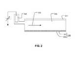
- FIG. 2illustrates a cross-sectional view of a portion of the integrated circuit device and flow cell according to an exemplary embodiment.
- FIGS. 3A and 3Billustrate cross-sectional and plan views respectively of a representative chemical sensors and corresponding reaction regions according to an exemplary embodiment.
- FIGS. 4 to 9illustrate stages in a manufacturing process for forming an array of chemical sensors and corresponding well structures according to an exemplary embodiment.
- a chemical detection deviceinclude low noise chemical sensors, such as chemically-sensitive field effect transistors (chemFETs), for detecting chemical reactions within overlying, operationally associated reaction regions.
- chemFETschemically-sensitive field effect transistors
- Chemical sensors with sensing surface areaswhich are not limited to a two-dimensional area at the bottom of the reaction regions.
- the sensing surface of the chemical sensorincludes a generally horizontal portion along the bottom surface of the reaction region, as well as a generally vertical portion on a sidewall of the reaction region.
- the chemical sensorBy extending the sensing surface in a generally vertical direction, the chemical sensor can have a small footprint, while also having a sufficiently large sensing surface area to avoid the noise issues associated with small sensing surfaces.
- the footprint of a chemical sensoris determined in part by the width (e.g. diameter) of the overlying reaction region and can be made small, allowing for a high density array.
- the sensing surfaceextends up the sidewall, the sensing surface area can be relatively large. As a result, low noise chemical sensors can be provided in a high density array, such that the characteristics of reactions can be accurately detected.
- FIG. 1illustrates a block diagram of components of a system for nucleic acid sequencing according to an exemplary embodiment.
- the componentsinclude a flow cell 101 on an integrated circuit device 100 , a reference electrode 108 , a plurality of reagents 114 for sequencing, a valve block 116 , a wash solution 110 , a valve 112 , a fluidics controller 118 , lines 120 / 122 / 126 , passages 104 / 109 / 111 , a waste container 106 , an array controller 124 , and a user interface 128 .
- the integrated circuit device 100includes a microwell array 107 overlying a sensor array that includes chemical sensors as described herein.
- the flow cell 101includes an inlet 102 , an outlet 103 , and a flow chamber 105 defining a flow path of reagents over the microwell array 107 .
- the reference electrode 108may be of any suitable type or shape, including a concentric cylinder with a fluid passage or a wire inserted into a lumen of passage 111 .
- the reagents 114may be driven through the fluid pathways, valves, and flow cell 101 by pumps, gas pressure, or other suitable methods, and may be discarded into the waste container 106 after exiting the outlet 103 of the flow cell 101 .
- the fluidics controller 118may control driving forces for the reagents 114 and the operation of valve 112 and valve block 116 with suitable software.
- the microwell array 107includes an array of reaction regions as described herein, also referred to herein as microwells, which are operationally associated with corresponding chemical sensors in the sensor array.
- each reaction regionmay be coupled to a chemical sensor suitable for detecting an analyte or reaction property of interest within that reaction region.
- the microwell array 107may be integrated in the integrated circuit device 100 , so that the microwell array 107 and the sensor array are part of a single device or chip.
- the flow cell 101may have a variety of configurations for controlling the path and flow rate of reagents 114 over the microwell array 107 .
- the array controller 124provides bias voltages and timing and control signals to the integrated circuit device 100 for reading the chemical sensors of the sensor array.
- the array controller 124also provides a reference bias voltage to the reference electrode 108 to bias the reagents 114 flowing over the microwell array 107 .
- the array controller 124collects and processes output signals from the chemical sensors of the sensor array through output ports on the integrated circuit device 100 via bus 127 .
- the array controller 124may be a computer or other computing means.
- the array controller 124may include memory for storage of data and software applications, a processor for accessing data and executing applications, and components that facilitate communication with the various components of the system in FIG. 1 .
- the values of the output signals of the chemical sensorsindicate physical and/or chemical parameters of one or more reactions taking place in the corresponding reaction regions in the microwell array 107 .
- the values of the output signalsmay be processed using the techniques disclosed in Rearick et al., U.S. patent application Ser. No. 13/339,846, filed Dec. 29, 2011, based on U.S. Prov. Pat. Appl. Nos. 61/428,743, filed Dec. 30, 2010, and 61/429,328, filed Jan. 3, 2011, and in Hubbell, U.S. patent application Ser. No. 13/339,753, filed Dec. 29, 2011, based on U.S. Prov. Pat. Appl. No. 61/428,097, filed Dec. 29, 2010, which are all incorporated by reference herein in their entirety.
- the user interface 128may display information about the flow cell 101 and the output signals received from chemical sensors in the sensor array on the integrated circuit device 100 .
- the user interface 128may also display instrument settings and controls, and allow a user to enter or set instrument settings and controls.
- the fluidics controller 118may control delivery of the individual reagents 114 to the flow cell 101 and integrated circuit device 100 in a predetermined sequence, for predetermined durations, at predetermined flow rates.
- the array controller 124can then collect and analyze the output signals of the chemical sensors indicating chemical reactions occurring in response to the delivery of the reagents 114 .
- the systemmay also monitor and control the temperature of the integrated circuit device 100 , so that reactions take place and measurements are made at a known predetermined temperature.
- the systemmay be configured to let a single fluid or reagent contact the reference electrode 108 throughout an entire multi-step reaction during operation.
- the valve 112may be shut to prevent any wash solution 110 from flowing into passage 109 as the reagents 114 are flowing. Although the flow of wash solution may be stopped, there may still be uninterrupted fluid and electrical communication between the reference electrode 108 , passage 109 , and the microwell array 107 .
- the distance between the reference electrode 108 and the junction between passages 109 and 111may be selected so that little or no amount of the reagents flowing in passage 109 and possibly diffusing into passage 111 reach the reference electrode 108 .
- the wash solution 110may be selected as being in continuous contact with the reference electrode 108 , which may be especially useful for multi-step reactions using frequent wash steps.
- FIG. 2illustrates cross-sectional and expanded views of a portion of the integrated circuit device 100 and flow cell 101 .
- the flow chamber 105 of the flow cell 101confines a reagent flow 208 of delivered reagents across open ends of the reaction regions in the microwell array 107 .
- the volume, shape, aspect ratio (such as base width-to-well depth ratio), and other dimensional characteristics of the reaction regionsmay be selected based on the nature of the reaction taking place, as well as the reagents, byproducts, or labeling techniques (if any) that are employed.
- the chemical sensors of the sensor array 205are responsive to (and generate output signals) chemical reactions within associated reaction regions in the microwell array 107 to detect an analyte or reaction property of interest.
- the chemical sensors of the sensor array 205may for example be chemically sensitive field-effect transistors (chemFETs), such as ion-sensitive field effect transistors (ISFETs). Examples of chemical sensors and array configurations that may be used in embodiments are described in U.S. Patent Application Publication No. 2010/0300559, No. 2010/0197507, No. 2010/0301398, No. 2010/0300895, No. 2010/0137143, and No. 2009/0026082, and U.S. Pat. No. 7,575,865, each which are incorporated by reference herein.
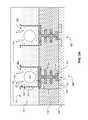
- FIG. 3Aillustrates a cross-sectional view of two representative chemical sensors and their corresponding reaction regions according to an exemplary embodiment.
- two chemical sensors 350 , 351are shown, representing a small portion of a sensor array that can include millions of chemical sensors.
- Chemical sensor 350is coupled to corresponding reaction region 301 , and chemical sensor 351 is coupled to corresponding reaction region 302 .
- Chemical sensor 350is representative of the chemical sensors in the sensor array.
- the chemical sensor 350is a chemically-sensitive field effect transistor (chemFET), more specifically an ion-sensitive field effect transistor (ISFET) in this example.
- chemFETchemically-sensitive field effect transistor
- ISFETion-sensitive field effect transistor
- the chemical sensor 350includes a floating gate structure 318 having a sensor plate 320 coupled to the reaction region 301 by an electrically conductive element 370 .
- the sensor plate 320is the uppermost floating gate conductor in the floating gate structure 318 .
- the floating gate structure 318includes multiple patterned layers of conductive material within layers of dielectric material 319 .
- the chemical sensor 350also includes a source region 321 and a drain region 322 within a semiconductor substrate 354 .
- the source region 321 and the drain region 322comprise doped semiconductor material having a conductivity type different from the conductivity type of the substrate 354 .
- the source region 321 and the drain region 322may comprise doped P-type semiconductor material, and the substrate may comprise doped N-type semiconductor material.
- Channel region 323separates the source region 321 and the drain region 322 .
- the floating gate structure 318overlies the channel region 323 , and is separated from the substrate 354 by a gate dielectric 352 .
- the gate dielectric 352may be for example silicon dioxide. Alternatively, other dielectrics may be used for the gate dielectric 352 .
- the reaction region 301is within an opening having a sidewall 303 extending through dielectric material 310 to the upper surface of the sensor plate 320 .
- the dielectric material 310may comprise one or more layers of material, such as silicon dioxide or silicon nitride.
- the dimensions of the openings, and their pitch,can vary from implementation to implementation.
- the openingscan have a characteristic diameter, defined as the square root of 4 times the plan view cross-sectional area (A) divided by Pi (e.g., sqrt(4*A/ ⁇ ), of not greater than 5 micrometers, such as not greater than 3.5 micrometers, not greater than 2.0 micrometers, not greater than 1.6 micrometers, not greater than 1.0 micrometers, not greater than 0.8 micrometers, not greater than 0.6 micrometers, not greater than 0.4 micrometers, not greater than 0.2 micrometers or even not greater than 0.1 micrometers.
- the chemical sensor 350includes a cup-shaped electrically conductive element 370 extending up the sidewall 303 of the dielectric material 310 .
- the electrically conductive element 370is a conformal layer of material on the upper surface of the sensor plate 320 , and extends up the sidewall 303 and over a portion of the upper surface 311 of the dielectric material 310 . As a result, the electrically conductive element 370 protrudes out of the opening in the dielectric material 310 and onto the upper surface 311 of the dielectric material 310 .
- the inner surface 371 of the electrically conductive element 370defines the reaction region 301 for the chemical sensor 350 . That is, there is no intervening deposited material layer between the inner surface 371 of the electrically conductive element 370 and the reaction region 301 . As a result of this structure, the inner surface 371 of the electrically conductive element 370 is cup-shaped and acts as the sensing surface for the chemical sensor 350 . In addition, because the electrically conductive element 370 protrudes out of the opening in the dielectric material 310 , the sensing surface area of the chemical sensor 350 is not limited by the surface area of the opening.
- the electrically conductive element 370may comprise one or more of a variety of different materials to facilitate sensitivity to particular ions (e.g. hydrogen ions).
- the cup-shaped electrically conductive element 370allows the chemical sensor 350 to have a small plan view area, while also having a sufficiently large surface area to avoid the noise issues associated with small sensing surfaces.
- the plan view area of the chemical sensoris determined in part by the width (or diameter) of the reaction region 301 and can be made small, allowing for a high density array.
- the sensing surfaceextends up the sidewall 303 and out of the reaction region 301 , the sensing surface area depends upon the depth and the circumference of the reaction region 301 , as well as the distance that the electrically conductive element 370 extends over the upper surface 311 , and can be relatively large.
- low noise chemical sensors 350 , 351can be provided in a high density array, such that the characteristics of reactions can be accurately detected.
- a thin oxide of the material of the electrically conductive element 370may be grown on the inner surface 371 which acts as a sensing material (e.g. an ion-sensitive sensing material) for the chemical sensor 350 .
- the electrically conductive element 370may be titanium nitride, and titanium oxide or titanium oxynitride may be grown on the inner surface 371 during manufacturing and/or during exposure to solutions during use. Whether an oxide is formed depends on the conductive material, the manufacturing processes performed, and the conditions under which the device is operated.
- the electrically conductive element 370is shown as a single layer of material. More generally, the electrically conductive element 370 may comprise one or more layers of a variety of electrically conductive materials, such as metals or ceramics, depending upon the implementation.
- the conductive materialcan be for example a metallic material or alloy thereof, or can be a ceramic material, or a combination thereof.
- An exemplary metallic materialincludes one of aluminum, copper, nickel, titanium, silver, gold, platinum, hafnium, lanthanum, tantalum, tungsten, iridium, zirconium, palladium, or a combination thereof.
- An exemplary ceramic materialincludes one of titanium nitride, titanium aluminum nitride, titanium oxynitride, tantalum nitride, or a combination thereof.
- an additional conformal sensing material(not shown) is deposited on the inner surface 371 of the electrically conductive element 370 and on the upper surface 311 of the dielectric material 310 .
- the sensing materialmay comprise one or more of a variety of different materials to facilitate sensitivity to particular ions.
- silicon nitride or silicon oxynitride, as well as metal oxides such as silicon oxide, aluminum or tantalum oxidesgenerally provide sensitivity to hydrogen ions
- sensing materials comprising polyvinyl chloride containing valinomycinprovide sensitivity to potassium ions.
- Materials sensitive to other ionssuch as sodium, silver, iron, bromine, iodine, calcium, and nitrate may also be used, depending upon the implementation.
- the inner surface 371 of the electrically conductive element 370surrounds the reaction region 301 .
- the opening and the reaction region 301have circular cross sections.
- the rim 390 of the portion of the conductive element 370 extending over the upper surface 311 of the dielectric material 310also has a circular cross section.
- thesemay be non-circular.
- the cross-sectionsmay be square, rectangular, hexagonal, or irregularly shaped.
- reactants, wash solutions, and other reagentsmay move in and out of the reaction region 301 by a diffusion mechanism 340 .
- the chemical sensor 350is responsive to (and generates an output signal related to) the amount of a charge 324 proximate to the electrically conductive element 370 .
- the presence of charge 324 in an analyte solutionalters the surface potential at the interface between the analyte solution and the inner surface 371 of the electrically conductive element 370 , due to the protonation or deprotonation of surface charge groups caused by the ions present in the analyte solution.
- Changes in the charge 324cause changes in the voltage on the floating gate structure 318 , which in turn changes in the threshold voltage of the transistor of the chemical sensor 350 .
- This change in threshold voltagecan be measured by measuring the current in the channel region 323 between the source region 321 and a drain region 322 .
- the chemical sensor 350can be used directly to provide a current-based output signal on an array line connected to the source region 321 or drain region 322 , or indirectly with additional circuitry to provide a voltage-based output signal.
- the distance that the electrically conductive element 370 extends away from the opening and over the upper surface 311 of the dielectric material 310is determined by dimensions of an etch mask used to pattern the electrically conductive element 370 . Because the charge 324 is more highly concentrated near the bottom of the reaction region 301 , in some embodiments variations in the dimensions of this extension does not have a significant effect on the amplitude of the signal detected in response to the charge 324 . In such a case, the formation of the etch mask used to define the electrically conductive element 370 may not require a critical alignment step.
- reactions carried out in the reaction region 301can be analytical reactions to identify or determine characteristics or properties of an analyte of interest. Such reactions can generate directly or indirectly byproducts that affect the amount of charge adjacent to the electrically conductive element 370 . If such byproducts are produced in small amounts or rapidly decay or react with other constituents, multiple copies of the same analyte may be analyzed in the reaction region 301 at the same time in order to increase the output signal generated. In an embodiment, multiple copies of an analyte may be attached to a solid phase support 312 , either before or after deposition into the reaction region 301 .
- the solid phase support 312may be microparticles, nanoparticles, beads, solid or porous comprising gels, or the like.
- solid phase support 312is also referred herein as a particle.
- multiple, connected copiesmay be made by rolling circle amplification (RCA), exponential RCA, or like techniques, to produce an amplicon without the need of a solid support.
- RCArolling circle amplification
- exponential RCAexponential RCA
- a nucleotide incorporation eventmay be determined by detecting ions (e.g., hydrogen ions) that are generated as natural by-products of polymerase-catalyzed nucleotide extension reactions. This may be used to sequence a sample or template nucleic acid, which may be a fragment of a nucleic acid sequence of interest, for example, and which may be directly or indirectly attached as a clonal population to a solid support, such as a particle, microparticle, bead, etc.
- ionse.g., hydrogen ions
- the sample or template nucleic acidmay be operably associated to a primer and polymerase and may be subjected to repeated cycles or “flows” of deoxynucleoside triphosphate (“dNTP”) addition (which may be referred to herein as “nucleotide flows” from which nucleotide incorporations may result) and washing.
- dNTPdeoxynucleoside triphosphate
- the primermay be annealed to the sample or template so that the primer's 3′ end can be extended by a polymerase whenever dNTPs complementary to the next base in the template are added.
- the identity of the type, sequence and number of nucleotide(s) associated with a sample nucleic acid present in a reaction region coupled to a chemical sensorcan be determined.
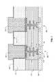
- FIGS. 4 to 9illustrate stages in a manufacturing process for forming an array of chemical sensors and corresponding well structures according to an exemplary embodiment.
- FIG. 4illustrates a first stage of forming a structure including a dielectric material 310 on the sensor plate 320 of the field effect transistor of the chemical sensor 350 .
- the structure in FIG. 4can be formed by depositing a layer of gate dielectric material on the semiconductor substrate 354 , and depositing a layer of polysilicon (or other electrically conductive material) on the layer of gate dielectric material.
- the layer of polysilicon and the layer gate dielectric materialcan then be etched using an etch mask to form the gate dielectric elements (e.g. gate dielectric 352 ) and the lowermost conductive material element of the floating gate structures.
- ion implantationcan then be performed to form the source and drain regions (e.g. source region 321 and a drain region 322 ) of the chemical sensors.
- a first layer of the dielectric material 319can then be deposited over the lowermost conductive material elements. Conductive plugs can then be formed within vias etched in the first layer of dielectric material 319 to contact the lowermost conductive material elements of the floating gate structures. A layer of conductive material can then be deposited on the first layer of the dielectric material 319 and patterned to form second conductive material elements electrically connected to the conductive plugs. This process can then be repeated multiple times to form the completed floating gate structure 318 shown in FIG. 4 . Alternatively, other and/or additional techniques may be performed to form the structure.
- Forming the structure in FIG. 4can also include forming additional elements such as array lines (e.g. word lines, bit lines, etc.) for accessing the chemical sensors, additional doped regions in the substrate 354 , and other circuitry (e.g. access circuitry, bias circuitry etc.) used to operate the chemical sensors, depending upon the device and array configuration in which the chemical sensors described herein are implemented.
- the elements of the structuremay for example be manufactured using techniques described in U.S. Patent Application Publication No. 2010/0300559, No. 2010/0197507, No. 2010/0301398, No. 2010/0300895, No. 2010/0137143, and No. 2009/0026082, and U.S. Pat. No. 7,575,865, each which are incorporated by reference herein.
- the dielectric material 310 of the structure in FIG. 4is etched to form openings 500 , 502 extending to the upper surfaces of the floating gate structures of the chemical sensors 350 , 351 , resulting in the structure illustrated in FIG. 5 .
- the openings 500 , 502may for example be formed by using a lithographic process to pattern a layer of photoresist on the dielectric material 310 to define the locations of the openings 500 , 502 , and then anisotropically etching the dielectric material 310 using the patterned photoresist as an etch mask.
- the anisotropic etching of the dielectric material 310may for example be a dry etch process, such as a fluorine based Reactive Ion Etching (RIE) process.
- RIEfluorine based Reactive Ion Etching
- the openings 500 , 502are separated by a distance 530 that is equal to their width 520 .
- the separation distance 530 between adjacent openingsmay be less than the width 520 .
- the separation distance 530may be a minimum feature size for the process (e.g. a lithographic process) used to form the openings 500 , 502 . In such a case, the distance 530 may be significantly less than the width 520 .
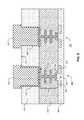
- the conductive material 600comprises one or more layers of electrically conductive material.
- the conductive material 600may be a layer of titanium nitride, or a layer of titanium.
- other and/or additional conductive materialsmay be used, such as those described above with reference to the electrically conductive element 370 .
- more than one layer of conductive materialmay be deposited.
- the conductive material 600may be deposited using various techniques, such as sputtering, reactive sputtering, atomic layer deposition (ALD), low pressure chemical vapor deposition (LPCVD), plasma enhanced chemical vapor deposition (PECVD), metal organic chemical vapor deposition (MOCVD), etc.
- ALDatomic layer deposition
- LPCVDlow pressure chemical vapor deposition
- PECVDplasma enhanced chemical vapor deposition
- MOCVDmetal organic chemical vapor deposition
- mask elements 700 , 702are formed within the openings 500 , 502 , resulting in the structure illustrated in FIG. 7 .
- the mask elements 700 , 702have widths greater than that of the openings 500 , 502 , so that the mask elements 700 , 702 extend over a portion of the upper surface 311 of the dielectric material 310 .
- the mask elements 700 , 702may for example be formed by patterning a layer of photoresist using a lithographic process. Alternatively, other materials and processes may be used to form the mask elements 700 , 702 .
- the conductive material 600is etched using the mask elements 700 , 702 as an etch mask, resulting in the structure illustrated in FIG. 8 .
- the etching processremoves exposed conductive material 600 from the upper surface 311 of the dielectric material 310 to form the cup-shaped electrically conductive elements 370 , 800 .
- the mask elements 700 , 702also protect the inner surfaces of the electrically conductive elements 370 , 800 , which subsequently act as the sensing surfaces for the chemical sensors 350 , 351 , during the etch process. In doing so, damage to the sensing surfaces can be avoided.
- the mask elements 700 , 702are removed to expose the electrically conductive elements 370 , 800 , resulting in the structure illustrated in FIG. 9 .
- the mask elements 700 , 702are patterned photoresist, they can be removed using a photoresist stripping process.
- the mask elements 700 , 702comprise other materials, other techniques may be used.
Landscapes
- Life Sciences & Earth Sciences (AREA)
- Chemical & Material Sciences (AREA)
- Health & Medical Sciences (AREA)
- Physics & Mathematics (AREA)
- Molecular Biology (AREA)
- Microelectronics & Electronic Packaging (AREA)
- Chemical Kinetics & Catalysis (AREA)
- Electrochemistry (AREA)
- Engineering & Computer Science (AREA)
- Analytical Chemistry (AREA)
- Biochemistry (AREA)
- General Health & Medical Sciences (AREA)
- General Physics & Mathematics (AREA)
- Immunology (AREA)
- Pathology (AREA)
- Investigating Or Analyzing Materials By The Use Of Electric Means (AREA)
Abstract
Description
The present disclosure relates to sensors for chemical analysis, and to methods for manufacturing such sensors.
A variety of types of chemical sensors have been used in the detection of chemical processes. One type is a chemically-sensitive field effect transistor (chemFET). A chemFET includes a source and a drain separated by a channel region, and a chemically sensitive area coupled to the channel region. The operation of the chemFET is based on the modulation of channel conductance, caused by changes in charge at the sensitive area due to a chemical reaction occurring nearby. The modulation of the channel conductance changes the threshold voltage of the chemFET, which can be measured to detect and/or determine characteristics of the chemical reaction. The threshold voltage may for example be measured by applying appropriate bias voltages to the source and drain, and measuring a resulting current flowing through the chemFET. As another example, the threshold voltage may be measured by driving a known current through the chemFET, and measuring a resulting voltage at the source or drain.
An ion-sensitive field effect transistor (ISFET) is a type of chemFET that includes an ion-sensitive layer at the sensitive area. The presence of ions in an analyte solution alters the surface potential at the interface between the ion-sensitive layer and the analyte solution, due to the protonation or deprotonation of surface charge groups caused by the ions present in the analyte solution. The change in surface potential at the sensitive area of the ISFET affects the threshold voltage of the device, which can be measured to indicate the presence and/or concentration of ions within the solution.
Arrays of ISFETs may be used for monitoring chemical reactions, such as DNA sequencing reactions, based on the detection of ions present, generated, or used during the reactions. See, for example, U.S. Pat. No. 7,948,015 to Rothberg et al., which is incorporated by reference herein. More generally, large arrays of chemFETs or other types of chemical sensors may be employed to detect and measure static and/or dynamic amounts or concentrations of a variety of analytes (e.g. hydrogen ions, other ions, compounds, etc.) in a variety of processes. The processes may for example be biological or chemical reactions, cell or tissue cultures or monitoring neural activity, nucleic acid sequencing, etc.
An issue that arises in the operation of large scale chemical sensor arrays is the susceptibility of the sensor output signals to noise. Specifically, the noise affects the accuracy of the downstream signal processing used to determine the characteristics of the chemical and/or biological process being detected by the sensors.
It is therefore desirable to provide devices including low noise chemical sensors, and methods for manufacturing such devices.
In one implementation, a chemical sensor is described. The chemical sensor includes a chemically-sensitive field effect transistor including a floating gate conductor having an upper surface. A dielectric material defines an opening extending to the upper surface of the floating gate conductor. A conductive element on a sidewall of the opening and extending over an upper surface of the dielectric material.
In another implementation, a method for manufacturing a chemical sensor is described. The method includes forming a chemically-sensitive field effect transistor including a floating gate conductor having an upper surface. The method further includes forming a dielectric material defining an opening extending to the upper surface of the floating gate conductor. The method further includes forming a conductive element on a sidewall of the opening and extending over an upper surface of the dielectric material.
Particular aspects of one more implementations of the subject matter described in this specification are set forth in the drawings and the description below. Other features, aspects, and advantages of the subject matter will become apparent from the description, the drawings, and the claims.
A chemical detection device are described that include low noise chemical sensors, such as chemically-sensitive field effect transistors (chemFETs), for detecting chemical reactions within overlying, operationally associated reaction regions.
Reducing the plan or top view area (or footprint) of individual chemical sensors and the overlying reaction regions allows for higher density devices. However, as the dimensions of the chemical sensors are reduced, Applicants have found that a corresponding reduction in the sensing surface area of the sensors can significantly impact performance.
For example, for chemical sensors having sensing surfaces defined at the bottom of the reaction regions, reducing the plan view dimensions (e.g. the width or diameter) of the reaction regions results in a similar reduction in the sensing surface areas. Applicants have found that as the sensing surface area is reduced to technology limits, fluidic noise due to the random fluctuation of charge on the sensing surface contributes to an increasing proportion of the total variation in sensing surface potential. This can significantly reduce the signal-to-noise ratio (SNR) of the sensor output signal, which affects the accuracy of the downstream signal processing used to determine the characteristics of the chemical and/or biological process being detected by the sensor.
Chemical sensors with sensing surface areas which are not limited to a two-dimensional area at the bottom of the reaction regions. In embodiments described herein, the sensing surface of the chemical sensor includes a generally horizontal portion along the bottom surface of the reaction region, as well as a generally vertical portion on a sidewall of the reaction region.
By extending the sensing surface in a generally vertical direction, the chemical sensor can have a small footprint, while also having a sufficiently large sensing surface area to avoid the noise issues associated with small sensing surfaces. The footprint of a chemical sensor is determined in part by the width (e.g. diameter) of the overlying reaction region and can be made small, allowing for a high density array. In addition, because the sensing surface extends up the sidewall, the sensing surface area can be relatively large. As a result, low noise chemical sensors can be provided in a high density array, such that the characteristics of reactions can be accurately detected.
Thereference electrode 108 may be of any suitable type or shape, including a concentric cylinder with a fluid passage or a wire inserted into a lumen ofpassage 111. Thereagents 114 may be driven through the fluid pathways, valves, andflow cell 101 by pumps, gas pressure, or other suitable methods, and may be discarded into thewaste container 106 after exiting theoutlet 103 of theflow cell 101. Thefluidics controller 118 may control driving forces for thereagents 114 and the operation ofvalve 112 andvalve block 116 with suitable software.
Themicrowell array 107 includes an array of reaction regions as described herein, also referred to herein as microwells, which are operationally associated with corresponding chemical sensors in the sensor array. For example, each reaction region may be coupled to a chemical sensor suitable for detecting an analyte or reaction property of interest within that reaction region. Themicrowell array 107 may be integrated in theintegrated circuit device 100, so that themicrowell array 107 and the sensor array are part of a single device or chip.
Theflow cell 101 may have a variety of configurations for controlling the path and flow rate ofreagents 114 over themicrowell array 107. Thearray controller 124 provides bias voltages and timing and control signals to theintegrated circuit device 100 for reading the chemical sensors of the sensor array. Thearray controller 124 also provides a reference bias voltage to thereference electrode 108 to bias thereagents 114 flowing over themicrowell array 107.
During an experiment, thearray controller 124 collects and processes output signals from the chemical sensors of the sensor array through output ports on theintegrated circuit device 100 viabus 127. Thearray controller 124 may be a computer or other computing means. Thearray controller 124 may include memory for storage of data and software applications, a processor for accessing data and executing applications, and components that facilitate communication with the various components of the system inFIG. 1 .
The values of the output signals of the chemical sensors indicate physical and/or chemical parameters of one or more reactions taking place in the corresponding reaction regions in themicrowell array 107. For example, in an exemplary embodiment, the values of the output signals may be processed using the techniques disclosed in Rearick et al., U.S. patent application Ser. No. 13/339,846, filed Dec. 29, 2011, based on U.S. Prov. Pat. Appl. Nos. 61/428,743, filed Dec. 30, 2010, and 61/429,328, filed Jan. 3, 2011, and in Hubbell, U.S. patent application Ser. No. 13/339,753, filed Dec. 29, 2011, based on U.S. Prov. Pat. Appl. No. 61/428,097, filed Dec. 29, 2010, which are all incorporated by reference herein in their entirety.
Theuser interface 128 may display information about theflow cell 101 and the output signals received from chemical sensors in the sensor array on theintegrated circuit device 100. Theuser interface 128 may also display instrument settings and controls, and allow a user to enter or set instrument settings and controls.
In an exemplary embodiment, during the experiment thefluidics controller 118 may control delivery of theindividual reagents 114 to theflow cell 101 andintegrated circuit device 100 in a predetermined sequence, for predetermined durations, at predetermined flow rates. Thearray controller 124 can then collect and analyze the output signals of the chemical sensors indicating chemical reactions occurring in response to the delivery of thereagents 114.
During the experiment, the system may also monitor and control the temperature of theintegrated circuit device 100, so that reactions take place and measurements are made at a known predetermined temperature.
The system may be configured to let a single fluid or reagent contact thereference electrode 108 throughout an entire multi-step reaction during operation. Thevalve 112 may be shut to prevent anywash solution 110 from flowing intopassage 109 as thereagents 114 are flowing. Although the flow of wash solution may be stopped, there may still be uninterrupted fluid and electrical communication between thereference electrode 108,passage 109, and themicrowell array 107. The distance between thereference electrode 108 and the junction betweenpassages passage 109 and possibly diffusing intopassage 111 reach thereference electrode 108. In an exemplary embodiment, thewash solution 110 may be selected as being in continuous contact with thereference electrode 108, which may be especially useful for multi-step reactions using frequent wash steps.
The chemical sensors of thesensor array 205 are responsive to (and generate output signals) chemical reactions within associated reaction regions in themicrowell array 107 to detect an analyte or reaction property of interest. The chemical sensors of thesensor array 205 may for example be chemically sensitive field-effect transistors (chemFETs), such as ion-sensitive field effect transistors (ISFETs). Examples of chemical sensors and array configurations that may be used in embodiments are described in U.S. Patent Application Publication No. 2010/0300559, No. 2010/0197507, No. 2010/0301398, No. 2010/0300895, No. 2010/0137143, and No. 2009/0026082, and U.S. Pat. No. 7,575,865, each which are incorporated by reference herein.
Thechemical sensor 350 includes a floatinggate structure 318 having asensor plate 320 coupled to thereaction region 301 by an electricallyconductive element 370. As can be seen inFIG. 3A , thesensor plate 320 is the uppermost floating gate conductor in the floatinggate structure 318. In the illustrated example, the floatinggate structure 318 includes multiple patterned layers of conductive material within layers ofdielectric material 319.
Thechemical sensor 350 also includes asource region 321 and adrain region 322 within asemiconductor substrate 354. Thesource region 321 and thedrain region 322 comprise doped semiconductor material having a conductivity type different from the conductivity type of thesubstrate 354. For example, thesource region 321 and thedrain region 322 may comprise doped P-type semiconductor material, and the substrate may comprise doped N-type semiconductor material.
As shown inFIG. 3A , thereaction region 301 is within an opening having asidewall 303 extending throughdielectric material 310 to the upper surface of thesensor plate 320. Thedielectric material 310 may comprise one or more layers of material, such as silicon dioxide or silicon nitride.
The dimensions of the openings, and their pitch, can vary from implementation to implementation. In some embodiments, the openings can have a characteristic diameter, defined as the square root of 4 times the plan view cross-sectional area (A) divided by Pi (e.g., sqrt(4*A/π), of not greater than 5 micrometers, such as not greater than 3.5 micrometers, not greater than 2.0 micrometers, not greater than 1.6 micrometers, not greater than 1.0 micrometers, not greater than 0.8 micrometers, not greater than 0.6 micrometers, not greater than 0.4 micrometers, not greater than 0.2 micrometers or even not greater than 0.1 micrometers.
Thechemical sensor 350 includes a cup-shaped electricallyconductive element 370 extending up thesidewall 303 of thedielectric material 310. The electricallyconductive element 370 is a conformal layer of material on the upper surface of thesensor plate 320, and extends up thesidewall 303 and over a portion of theupper surface 311 of thedielectric material 310. As a result, the electricallyconductive element 370 protrudes out of the opening in thedielectric material 310 and onto theupper surface 311 of thedielectric material 310.
In the illustrated embodiment, theinner surface 371 of the electricallyconductive element 370 defines thereaction region 301 for thechemical sensor 350. That is, there is no intervening deposited material layer between theinner surface 371 of the electricallyconductive element 370 and thereaction region 301. As a result of this structure, theinner surface 371 of the electricallyconductive element 370 is cup-shaped and acts as the sensing surface for thechemical sensor 350. In addition, because the electricallyconductive element 370 protrudes out of the opening in thedielectric material 310, the sensing surface area of thechemical sensor 350 is not limited by the surface area of the opening. The electricallyconductive element 370 may comprise one or more of a variety of different materials to facilitate sensitivity to particular ions (e.g. hydrogen ions).
The cup-shaped electricallyconductive element 370 allows thechemical sensor 350 to have a small plan view area, while also having a sufficiently large surface area to avoid the noise issues associated with small sensing surfaces. The plan view area of the chemical sensor is determined in part by the width (or diameter) of thereaction region 301 and can be made small, allowing for a high density array. In addition, because the sensing surface extends up thesidewall 303 and out of thereaction region 301, the sensing surface area depends upon the depth and the circumference of thereaction region 301, as well as the distance that the electricallyconductive element 370 extends over theupper surface 311, and can be relatively large. As a result, lownoise chemical sensors
During manufacturing and/or operation of the device, a thin oxide of the material of the electricallyconductive element 370 may be grown on theinner surface 371 which acts as a sensing material (e.g. an ion-sensitive sensing material) for thechemical sensor 350. For example, in one embodiment the electricallyconductive element 370 may be titanium nitride, and titanium oxide or titanium oxynitride may be grown on theinner surface 371 during manufacturing and/or during exposure to solutions during use. Whether an oxide is formed depends on the conductive material, the manufacturing processes performed, and the conditions under which the device is operated.
In the illustrated example, the electricallyconductive element 370 is shown as a single layer of material. More generally, the electricallyconductive element 370 may comprise one or more layers of a variety of electrically conductive materials, such as metals or ceramics, depending upon the implementation. The conductive material can be for example a metallic material or alloy thereof, or can be a ceramic material, or a combination thereof. An exemplary metallic material includes one of aluminum, copper, nickel, titanium, silver, gold, platinum, hafnium, lanthanum, tantalum, tungsten, iridium, zirconium, palladium, or a combination thereof. An exemplary ceramic material includes one of titanium nitride, titanium aluminum nitride, titanium oxynitride, tantalum nitride, or a combination thereof.
In some alternative embodiments, an additional conformal sensing material (not shown) is deposited on theinner surface 371 of the electricallyconductive element 370 and on theupper surface 311 of thedielectric material 310. The sensing material may comprise one or more of a variety of different materials to facilitate sensitivity to particular ions. For example, silicon nitride or silicon oxynitride, as well as metal oxides such as silicon oxide, aluminum or tantalum oxides, generally provide sensitivity to hydrogen ions, whereas sensing materials comprising polyvinyl chloride containing valinomycin provide sensitivity to potassium ions. Materials sensitive to other ions such as sodium, silver, iron, bromine, iodine, calcium, and nitrate may also be used, depending upon the implementation.
As shown in the plan view ofFIG. 3B , theinner surface 371 of the electricallyconductive element 370 surrounds thereaction region 301. In the illustrated example the opening and thereaction region 301 have circular cross sections. In addition, therim 390 of the portion of theconductive element 370 extending over theupper surface 311 of thedielectric material 310 also has a circular cross section. Alternatively, these may be non-circular. For example, the cross-sections may be square, rectangular, hexagonal, or irregularly shaped.
Referring back toFIG. 3A , in operation, reactants, wash solutions, and other reagents may move in and out of thereaction region 301 by adiffusion mechanism 340. Thechemical sensor 350 is responsive to (and generates an output signal related to) the amount of acharge 324 proximate to the electricallyconductive element 370. The presence ofcharge 324 in an analyte solution alters the surface potential at the interface between the analyte solution and theinner surface 371 of the electricallyconductive element 370, due to the protonation or deprotonation of surface charge groups caused by the ions present in the analyte solution. Changes in thecharge 324 cause changes in the voltage on the floatinggate structure 318, which in turn changes in the threshold voltage of the transistor of thechemical sensor 350. This change in threshold voltage can be measured by measuring the current in thechannel region 323 between thesource region 321 and adrain region 322. As a result, thechemical sensor 350 can be used directly to provide a current-based output signal on an array line connected to thesource region 321 or drainregion 322, or indirectly with additional circuitry to provide a voltage-based output signal.
As described in more detail below with respect toFIGS. 4-9 , the distance that the electricallyconductive element 370 extends away from the opening and over theupper surface 311 of thedielectric material 310 is determined by dimensions of an etch mask used to pattern the electricallyconductive element 370. Because thecharge 324 is more highly concentrated near the bottom of thereaction region 301, in some embodiments variations in the dimensions of this extension does not have a significant effect on the amplitude of the signal detected in response to thecharge 324. In such a case, the formation of the etch mask used to define the electricallyconductive element 370 may not require a critical alignment step.
In an embodiment, reactions carried out in thereaction region 301 can be analytical reactions to identify or determine characteristics or properties of an analyte of interest. Such reactions can generate directly or indirectly byproducts that affect the amount of charge adjacent to the electricallyconductive element 370. If such byproducts are produced in small amounts or rapidly decay or react with other constituents, multiple copies of the same analyte may be analyzed in thereaction region 301 at the same time in order to increase the output signal generated. In an embodiment, multiple copies of an analyte may be attached to asolid phase support 312, either before or after deposition into thereaction region 301. Thesolid phase support 312 may be microparticles, nanoparticles, beads, solid or porous comprising gels, or the like. For simplicity and ease of explanation,solid phase support 312 is also referred herein as a particle. For a nucleic acid analyte, multiple, connected copies may be made by rolling circle amplification (RCA), exponential RCA, or like techniques, to produce an amplicon without the need of a solid support.
In various exemplary embodiments, the methods, systems, and computer readable media described herein may advantageously be used to process and/or analyze data and signals obtained from electronic or charged-based nucleic acid sequencing. In electronic or charged-based sequencing (such as, pH-based sequencing), a nucleotide incorporation event may be determined by detecting ions (e.g., hydrogen ions) that are generated as natural by-products of polymerase-catalyzed nucleotide extension reactions. This may be used to sequence a sample or template nucleic acid, which may be a fragment of a nucleic acid sequence of interest, for example, and which may be directly or indirectly attached as a clonal population to a solid support, such as a particle, microparticle, bead, etc. The sample or template nucleic acid may be operably associated to a primer and polymerase and may be subjected to repeated cycles or “flows” of deoxynucleoside triphosphate (“dNTP”) addition (which may be referred to herein as “nucleotide flows” from which nucleotide incorporations may result) and washing. The primer may be annealed to the sample or template so that the primer's 3′ end can be extended by a polymerase whenever dNTPs complementary to the next base in the template are added. Then, based on the known sequence of nucleotide flows and on measured output signals of the chemical sensors indicative of ion concentration during each nucleotide flow, the identity of the type, sequence and number of nucleotide(s) associated with a sample nucleic acid present in a reaction region coupled to a chemical sensor can be determined.
A first layer of thedielectric material 319 can then be deposited over the lowermost conductive material elements. Conductive plugs can then be formed within vias etched in the first layer ofdielectric material 319 to contact the lowermost conductive material elements of the floating gate structures. A layer of conductive material can then be deposited on the first layer of thedielectric material 319 and patterned to form second conductive material elements electrically connected to the conductive plugs. This process can then be repeated multiple times to form the completed floatinggate structure 318 shown inFIG. 4 . Alternatively, other and/or additional techniques may be performed to form the structure.
Forming the structure inFIG. 4 can also include forming additional elements such as array lines (e.g. word lines, bit lines, etc.) for accessing the chemical sensors, additional doped regions in thesubstrate 354, and other circuitry (e.g. access circuitry, bias circuitry etc.) used to operate the chemical sensors, depending upon the device and array configuration in which the chemical sensors described herein are implemented. In some embodiments, the elements of the structure may for example be manufactured using techniques described in U.S. Patent Application Publication No. 2010/0300559, No. 2010/0197507, No. 2010/0301398, No. 2010/0300895, No. 2010/0137143, and No. 2009/0026082, and U.S. Pat. No. 7,575,865, each which are incorporated by reference herein.
Next, thedielectric material 310 of the structure inFIG. 4 is etched to formopenings chemical sensors FIG. 5 .
Theopenings dielectric material 310 to define the locations of theopenings dielectric material 310 using the patterned photoresist as an etch mask. The anisotropic etching of thedielectric material 310 may for example be a dry etch process, such as a fluorine based Reactive Ion Etching (RIE) process.
In the illustrated embodiment, theopenings distance 530 that is equal to theirwidth 520. Alternatively, theseparation distance 530 between adjacent openings may be less than thewidth 520. For example, theseparation distance 530 may be a minimum feature size for the process (e.g. a lithographic process) used to form theopenings distance 530 may be significantly less than thewidth 520.
Next, a conformal layer ofconductive material 600 is deposited on the structure illustrated inFIG. 5 , resulting in the structure illustrated inFIG. 6 . Theconductive material 600 comprises one or more layers of electrically conductive material. For example, theconductive material 600 may be a layer of titanium nitride, or a layer of titanium. Alternatively, other and/or additional conductive materials may be used, such as those described above with reference to the electricallyconductive element 370. In addition, more than one layer of conductive material may be deposited.
Theconductive material 600 may be deposited using various techniques, such as sputtering, reactive sputtering, atomic layer deposition (ALD), low pressure chemical vapor deposition (LPCVD), plasma enhanced chemical vapor deposition (PECVD), metal organic chemical vapor deposition (MOCVD), etc.
Next,mask elements openings FIG. 7 . As shown inFIG. 7 , themask elements openings mask elements upper surface 311 of thedielectric material 310.
Themask elements mask elements
Next, theconductive material 600 is etched using themask elements FIG. 8 . The etching process removes exposedconductive material 600 from theupper surface 311 of thedielectric material 310 to form the cup-shaped electricallyconductive elements
Themask elements conductive elements chemical sensors
Next, themask elements conductive elements FIG. 9 . In embodiments in which themask elements mask elements
While the present invention is disclosed by reference to the preferred embodiments and examples detailed above, it is to be understood that these examples are intended in an illustrative rather than in a limiting sense. It is contemplated that modifications and combinations will readily occur to those skilled in the art, which modifications and combinations will be within the spirit of the invention and the scope of the following claims.
Claims (18)
1. A chemical sensor, comprising:
a chemically-sensitive field effect transistor including a floating gate conductor having an upper surface;
a dielectric material defining an opening extending to the upper surface of the floating gate conductor;
a conductive element on a sidewall of the opening and extending over an upper surface of the dielectric material, wherein
the chemically-sensitive field effect transistor includes a floating gate structure comprising a plurality of conductors electrically coupled to one another and separated by dielectric layers, and the floating gate conductor is an uppermost conductor in the plurality of conductors.
2. The chemical sensor ofclaim 1 , wherein the conductive element includes an inner surface defining a reaction region for the chemical sensor.
3. The chemical sensor ofclaim 1 , wherein the conductive element extends across the upper surface of the floating gate conductor to define a bottom surface of a reaction region for the chemical sensor.
4. The chemical sensor ofclaim 1 , wherein the conductive element comprises an electrically conductive material, and an inner surface of the conductive element includes an oxide of the electrically conductive material.
5. The chemical sensor ofclaim 1 , further comprising a layer of sensing material on the conductive element.
6. The chemical sensor ofclaim 5 , wherein the sensing material comprises a metal-oxide.
7. The chemical sensor ofclaim 1 , wherein a sensing surface for the chemical sensor includes an inner surface of the conductive element.
8. The chemical sensor ofclaim 7 , wherein the sensing surface is sensitive to hydrogen ions.
9. The chemical sensor ofclaim 1 , wherein the chemically-sensitive field effect transistor generates a sensor signal in response to a chemical reaction occurring proximate to the conductive element.
10. A chemical sensor, comprising:
a chemically-sensitive field effect transistor including a floating gate conductor having an upper surface;
a dielectric material defining an opening extending to the upper surface of the floating gate conductor;
a conductive element on a sidewall of the opening and extending over an upper surface of the dielectric material, wherein the conductive element does not extend into a second opening of an adjacent chemically-sensitive field effect transistor.
11. A method for manufacturing a chemical sensor, the method comprising:
forming a chemically-sensitive field effect transistor including a floating gate conductor having an upper surface;
forming a dielectric material defining an opening extending to the upper surface of the floating gate conductor; and
forming a conductive element on a sidewall of the opening and extending over an upper surface of the dielectric material, wherein forming the conductive element includes
depositing a conductive material within the opening and on the upper surface of the dielectric material,
forming a mask element within the opening and over at least a portion of the upper surface of the dielectric material, and
etching the conductive material using the mask element as an etch mask, thereby forming the conductive element.
12. The method ofclaim 11 , wherein forming the mask element comprises performing a lithographic process.
13. The method ofclaim 11 , wherein:
forming the mask element exposes conductive material on a second portion of the upper surface of the dielectric material; and
etching the conductive material removes the exposed conductive material.
14. The method ofclaim 11 , wherein the conductive element includes an inner surface defining a reaction region for the chemical sensor.
15. The method ofclaim 11 , wherein forming the conductive element includes forming the conductive element on the upper surface of the floating gate conductor to define a bottom surface of a reaction region for the chemical sensor.
16. The method ofclaim 11 , wherein the conductive element comprises an electrically conductive material, and an inner surface of the conductive element includes an oxide of the electrically conductive material.
17. The method ofclaim 11 , further comprising forming a layer of sensing material on the conductive element.
18. The method ofclaim 11 , wherein a sensing surface for the chemical sensor includes an inner surface of the conductive element.
Priority Applications (1)
| Application Number | Priority Date | Filing Date | Title |
|---|---|---|---|
| US13/801,243US8841217B1 (en) | 2013-03-13 | 2013-03-13 | Chemical sensor with protruded sensor surface |
Applications Claiming Priority (1)
| Application Number | Priority Date | Filing Date | Title |
|---|---|---|---|
| US13/801,243US8841217B1 (en) | 2013-03-13 | 2013-03-13 | Chemical sensor with protruded sensor surface |
Publications (2)
| Publication Number | Publication Date |
|---|---|
| US20140264466A1 US20140264466A1 (en) | 2014-09-18 |
| US8841217B1true US8841217B1 (en) | 2014-09-23 |
Family
ID=51523652
Family Applications (1)
| Application Number | Title | Priority Date | Filing Date |
|---|---|---|---|
| US13/801,243ActiveUS8841217B1 (en) | 2013-03-13 | 2013-03-13 | Chemical sensor with protruded sensor surface |
Country Status (1)
| Country | Link |
|---|---|
| US (1) | US8841217B1 (en) |
Cited By (29)
| Publication number | Priority date | Publication date | Assignee | Title |
|---|---|---|---|---|
| US20140264464A1 (en)* | 2013-03-13 | 2014-09-18 | Life Technologies Corporation | Chemical sensor with sidewall spacer sensor surface |
| US20140264322A1 (en)* | 2013-03-15 | 2014-09-18 | Life Technologies Corporation | Chemical sensor with protruded sensor surface |
| US9110015B2 (en) | 2010-09-24 | 2015-08-18 | Life Technologies Corporation | Method and system for delta double sampling |
| US9164070B2 (en) | 2010-06-30 | 2015-10-20 | Life Technologies Corporation | Column adc |
| US9239313B2 (en) | 2010-06-30 | 2016-01-19 | Life Technologies Corporation | Ion-sensing charge-accumulation circuits and methods |
| US9269708B2 (en) | 2006-12-14 | 2016-02-23 | Life Technologies Corporation | Methods and apparatus for measuring analytes using large scale FET arrays |
| US9270264B2 (en) | 2012-05-29 | 2016-02-23 | Life Technologies Corporation | System for reducing noise in a chemical sensor array |
| US9404920B2 (en) | 2006-12-14 | 2016-08-02 | Life Technologies Corporation | Methods and apparatus for detecting molecular interactions using FET arrays |
| US9618475B2 (en) | 2010-09-15 | 2017-04-11 | Life Technologies Corporation | Methods and apparatus for measuring analytes |
| US9671363B2 (en) | 2013-03-15 | 2017-06-06 | Life Technologies Corporation | Chemical sensor with consistent sensor surface areas |
| US9823217B2 (en) | 2013-03-15 | 2017-11-21 | Life Technologies Corporation | Chemical device with thin conductive element |
| US9841398B2 (en) | 2013-01-08 | 2017-12-12 | Life Technologies Corporation | Methods for manufacturing well structures for low-noise chemical sensors |
| US9852919B2 (en) | 2013-01-04 | 2017-12-26 | Life Technologies Corporation | Methods and systems for point of use removal of sacrificial material |
| US9927393B2 (en) | 2009-05-29 | 2018-03-27 | Life Technologies Corporation | Methods and apparatus for measuring analytes |
| US9951382B2 (en) | 2006-12-14 | 2018-04-24 | Life Technologies Corporation | Methods and apparatus for measuring analytes using large scale FET arrays |
| US9960253B2 (en) | 2010-07-03 | 2018-05-01 | Life Technologies Corporation | Chemically sensitive sensor with lightly doped drains |
| US9964515B2 (en) | 2008-10-22 | 2018-05-08 | Life Technologies Corporation | Integrated sensor arrays for biological and chemical analysis |
| US9970984B2 (en) | 2011-12-01 | 2018-05-15 | Life Technologies Corporation | Method and apparatus for identifying defects in a chemical sensor array |
| US10048220B2 (en)* | 2015-10-08 | 2018-08-14 | Taiwan Semiconductor Manufacturing Company Ltd. | Biosensor field effect transistor having specific well structure and method of forming the same |
| US10077472B2 (en) | 2014-12-18 | 2018-09-18 | Life Technologies Corporation | High data rate integrated circuit with power management |
| US10100357B2 (en) | 2013-05-09 | 2018-10-16 | Life Technologies Corporation | Windowed sequencing |
| US10379079B2 (en) | 2014-12-18 | 2019-08-13 | Life Technologies Corporation | Methods and apparatus for measuring analytes using large scale FET arrays |
| US10451585B2 (en) | 2009-05-29 | 2019-10-22 | Life Technologies Corporation | Methods and apparatus for measuring analytes |
| US10458942B2 (en) | 2013-06-10 | 2019-10-29 | Life Technologies Corporation | Chemical sensor array having multiple sensors per well |
| US10605767B2 (en) | 2014-12-18 | 2020-03-31 | Life Technologies Corporation | High data rate integrated circuit with transmitter configuration |
| US10718733B2 (en) | 2009-05-29 | 2020-07-21 | Life Technologies Corporation | Methods and apparatus for measuring analytes |
| US11231451B2 (en) | 2010-06-30 | 2022-01-25 | Life Technologies Corporation | Methods and apparatus for testing ISFET arrays |
| US11307166B2 (en) | 2010-07-01 | 2022-04-19 | Life Technologies Corporation | Column ADC |
| US11339430B2 (en) | 2007-07-10 | 2022-05-24 | Life Technologies Corporation | Methods and apparatus for measuring analytes using large scale FET arrays |
Families Citing this family (2)
| Publication number | Priority date | Publication date | Assignee | Title |
|---|---|---|---|---|
| CN107923869B (en)* | 2015-08-25 | 2021-10-08 | 生命技术公司 | Design of deep microwell and method of making the same |
| US10890554B1 (en)* | 2019-06-20 | 2021-01-12 | Globalfoundries Singapore Pte. Ltd. | Sensors with a non-planar sensing structure |
Citations (325)
| Publication number | Priority date | Publication date | Assignee | Title |
|---|---|---|---|---|
| US4086642A (en) | 1975-01-16 | 1978-04-25 | Hitachi, Ltd. | Protective circuit and device for metal-oxide-semiconductor field effect transistor and method for fabricating the device |
| JPS5870155U (en) | 1981-11-06 | 1983-05-12 | ヤマハ株式会社 | Electronic equipment storage furniture |
| US4411741A (en) | 1982-01-12 | 1983-10-25 | University Of Utah | Apparatus and method for measuring the concentration of components in fluids |
| US4490678A (en) | 1981-05-15 | 1984-12-25 | Licentia Patent-Verwaltungs-G.M.B.H. | Method of and an apparatus for measuring ion concentrations in solutions |
| US4641084A (en) | 1983-12-15 | 1987-02-03 | Olympus Optical Co., Ltd. | Ion concentration measuring apparatus |
| EP0223618A3 (en) | 1985-07-18 | 1987-07-08 | New York Medical College | Automatable process for nucleotide sequencing |
| US4691167A (en) | 1983-08-24 | 1987-09-01 | Sentron V.O.F. | Apparatus for determining the activity of an ion (pIon) in a liquid |
| US4701253A (en) | 1983-11-03 | 1987-10-20 | Sentron V.O.F. | ISFET-based measuring device and method for correcting drift |
| US4722830A (en) | 1986-05-05 | 1988-02-02 | General Electric Company | Automated multiple stream analysis system |
| US4743954A (en) | 1985-06-07 | 1988-05-10 | University Of Utah | Integrated circuit for a chemical-selective sensor with voltage output |
| US4764797A (en) | 1985-09-14 | 1988-08-16 | Thorn Emi Plc | Chemical-sensitive semiconductor device |
| US4777019A (en) | 1985-04-12 | 1988-10-11 | Thomas Dandekar | Biosensor |
| US4822566A (en) | 1985-11-19 | 1989-04-18 | The Johns Hopkins University | Optimized capacitive sensor for chemical analysis and measurement |
| US4864229A (en) | 1986-05-03 | 1989-09-05 | Integrated Ionics, Inc. | Method and apparatus for testing chemical and ionic sensors |
| WO1989009283A1 (en) | 1988-03-25 | 1989-10-05 | Edward David Hyman | Pyrophosphate-based method and apparatus for sequencing nucleic acids |
| US4874499A (en) | 1988-05-23 | 1989-10-17 | Massachusetts Institute Of Technology | Electrochemical microsensors and method of making such sensors |
| US5009766A (en) | 1988-02-08 | 1991-04-23 | I-Stat Corporation | Metal oxide electrodes |
| US5038192A (en) | 1989-04-28 | 1991-08-06 | International Business Machines Corporation | Gate array cell having FETs of different and optimized sizes |
| US5110441A (en) | 1989-12-14 | 1992-05-05 | Monsanto Company | Solid state ph sensor |
| US5113870A (en) | 1987-05-01 | 1992-05-19 | Rossenfeld Joel P | Method and apparatus for the analysis, display and classification of event related potentials by interpretation of P3 responses |
| US5138251A (en) | 1989-10-04 | 1992-08-11 | Olympus Optical Co., Ltd. | Fet sensor apparatus of flow-cell adaptive type and method of manufacturing the same |
| US5151759A (en) | 1989-03-02 | 1992-09-29 | Thunderbird Technologies, Inc. | Fermi threshold silicon-on-insulator field effect transistor |
| US5164319A (en) | 1985-08-22 | 1992-11-17 | Molecular Devices Corporation | Multiple chemically modulated capacitance determination |
| JPH0577210B2 (en) | 1986-09-04 | 1993-10-26 | Tamura Seisakusho Kk | |
| US5284566A (en) | 1993-01-04 | 1994-02-08 | Bacharach, Inc. | Electrochemical gas sensor with wraparound reference electrode |
| JPH06138846A (en) | 1992-10-29 | 1994-05-20 | Hitachi Ltd | Liquid crystal half-tone display system |
| US5317407A (en) | 1991-03-11 | 1994-05-31 | General Electric Company | Fixed-pattern noise correction circuitry for solid-state imager |
| US5319226A (en) | 1991-09-06 | 1994-06-07 | Dong Jin Kim | Method of fabricating an ion sensitive field effect transistor with a Ta2 O5 hydrogen ion sensing membrane |
| US5407854A (en) | 1994-01-19 | 1995-04-18 | General Signal Corporation | ESD protection of ISFET sensors |
| US5436149A (en) | 1993-02-19 | 1995-07-25 | Barnes; Wayne M. | Thermostable DNA polymerase with enhanced thermostability and enhanced length and efficiency of primer extension |
| US5439839A (en) | 1994-07-13 | 1995-08-08 | Winbond Electronics Corporation | Self-aligned source/drain MOS process |
| US5466348A (en) | 1991-10-21 | 1995-11-14 | Holm-Kennedy; James W. | Methods and devices for enhanced biochemical sensing |
| US5490971A (en) | 1994-10-25 | 1996-02-13 | Sippican, Inc. | Chemical detector |
| US5554339A (en) | 1988-11-14 | 1996-09-10 | I-Stat Corporation | Process for the manufacture of wholly microfabricated biosensors |
| US5583462A (en) | 1993-04-26 | 1996-12-10 | Unifet Incorporated | Method and apparatus for multiplexing devices having long thermal time constants |
| US5593838A (en) | 1994-11-10 | 1997-01-14 | David Sarnoff Research Center, Inc. | Partitioned microelectronic device array |
| US5600451A (en) | 1993-08-12 | 1997-02-04 | Sony Corporation | Charge transfer device and output circuit thereof |
| US5631704A (en) | 1994-10-14 | 1997-05-20 | Lucent Technologies, Inc. | Active pixel sensor and imaging system having differential mode |
| US5637469A (en) | 1992-05-01 | 1997-06-10 | Trustees Of The University Of Pennsylvania | Methods and apparatus for the detection of an analyte utilizing mesoscale flow systems |
| US5702964A (en) | 1995-10-17 | 1997-12-30 | Lg Semicon, Co., Ltd. | Method for forming a semiconductor device having a floating gate |
| WO1998013523A1 (en) | 1996-09-27 | 1998-04-02 | Pyrosequencing Ab | Method of sequencing dna |
| US5793230A (en) | 1997-02-26 | 1998-08-11 | Sandia Corporation | Sensor readout detector circuit |
| WO1998046797A1 (en) | 1997-04-16 | 1998-10-22 | Immunological Associates Of Denver | Nucleic acid archiving |
| US5846708A (en) | 1991-11-19 | 1998-12-08 | Massachusetts Institiute Of Technology | Optical and electrical methods and apparatus for molecule detection |
| US5911873A (en) | 1997-05-02 | 1999-06-15 | Rosemount Analytical Inc. | Apparatus and method for operating an ISFET at multiple drain currents and gate-source voltages allowing for diagnostics and control of isopotential points |
| US5912560A (en) | 1997-02-25 | 1999-06-15 | Waferscale Integration Inc. | Charge pump circuit for voltage boosting in integrated semiconductor circuits |
| US5923421A (en) | 1997-07-24 | 1999-07-13 | Lockheed Martin Energy Research Corporation | Chemical detection using calorimetric spectroscopy |
| US5922591A (en) | 1995-06-29 | 1999-07-13 | Affymetrix, Inc. | Integrated nucleic acid diagnostic device |
| US5958703A (en) | 1996-12-03 | 1999-09-28 | Glaxo Group Limited | Use of modified tethers in screening compound libraries |
| US5965452A (en) | 1996-07-09 | 1999-10-12 | Nanogen, Inc. | Multiplexed active biologic array |
| US6002299A (en) | 1997-06-10 | 1999-12-14 | Cirrus Logic, Inc. | High-order multipath operational amplifier with dynamic offset reduction, controlled saturation current limiting, and current feedback for enhanced conditional stability |
| US6107032A (en) | 1996-12-20 | 2000-08-22 | Roche Diagnostics Gmbh | Method for the direct, exponential amplification and sequencing of DNA molecules and its application |
| US6195585B1 (en) | 1998-06-26 | 2001-02-27 | Advanced Bionics Corporation | Remote monitoring of implantable cochlear stimulator |
| US6255678B1 (en) | 1997-05-29 | 2001-07-03 | Horiba, Ltd. | Apparatus for measuring physical and chemical phenomena |
| US6262568B1 (en) | 1999-12-14 | 2001-07-17 | Matsushita Electric Industrial Co., Ltd. | Common mode bias generator |
| US6274320B1 (en) | 1999-09-16 | 2001-08-14 | Curagen Corporation | Method of sequencing a nucleic acid |
| WO2001081896A1 (en) | 2000-04-24 | 2001-11-01 | Eagle Research & Development, Llc | An ultra-fast nucleic acid sequencing device and a method for making and using the same |
| US6327410B1 (en) | 1997-03-14 | 2001-12-04 | The Trustees Of Tufts College | Target analyte sensors utilizing Microspheres |
| US6355431B1 (en) | 1999-04-20 | 2002-03-12 | Illumina, Inc. | Detection of nucleic acid amplification reactions using bead arrays |
| US6361671B1 (en) | 1999-01-11 | 2002-03-26 | The Regents Of The University Of California | Microfabricated capillary electrophoresis chip and method for simultaneously detecting multiple redox labels |
| US20020042388A1 (en) | 2001-05-01 | 2002-04-11 | Cooper Mark J. | Lyophilizable and enhanced compacted nucleic acids |
| US6384684B1 (en) | 1999-11-13 | 2002-05-07 | U.S. Philips Corporation | Amplifier |
| US6403957B1 (en) | 1989-06-07 | 2002-06-11 | Affymetrix, Inc. | Nucleic acid reading and analysis system |
| US6406848B1 (en) | 1997-05-23 | 2002-06-18 | Lynx Therapeutics, Inc. | Planar arrays of microparticle-bound polynucleotides |
| US6413792B1 (en) | 2000-04-24 | 2002-07-02 | Eagle Research Development, Llc | Ultra-fast nucleic acid sequencing device and a method for making and using the same |
| US6429027B1 (en) | 1998-12-28 | 2002-08-06 | Illumina, Inc. | Composite arrays utilizing microspheres |
| US6432360B1 (en) | 1997-10-10 | 2002-08-13 | President And Fellows Of Harvard College | Replica amplification of nucleic acid arrays |
| US6433386B1 (en) | 1997-10-20 | 2002-08-13 | Samsung Electronics Co., Ltd. | Sense FET having a selectable sense current ratio and method of manufacturing the same |
| JP2002272463A (en) | 2001-03-22 | 2002-09-24 | Olympus Optical Co Ltd | Method for judging form of monobasic polymorphism |
| US6459398B1 (en) | 1999-07-20 | 2002-10-01 | D.S.P.C. Technologies Ltd. | Pulse modulated digital to analog converter (DAC) |
| WO2002077287A1 (en) | 2001-03-21 | 2002-10-03 | Curagen Corporation | Apparatus and method for sequencing a nucleic acid |
| US6465178B2 (en) | 1997-09-30 | 2002-10-15 | Surmodics, Inc. | Target molecule attachment to surfaces |
| US20020150909A1 (en) | 1999-02-09 | 2002-10-17 | Stuelpnagel John R. | Automated information processing in randomly ordered arrays |
| WO2002086162A1 (en) | 2001-04-23 | 2002-10-31 | Samsung Electronics Co., Ltd. | Molecular detection chip including mosfet, molecular detection device employing the chip, and molecular detection method using the device |
| US6475728B1 (en) | 1997-06-11 | 2002-11-05 | Ecole Centrale De Lyon | Method for identifying and/or analyzing biological substances, present in a conductive liquid, device and affinity sensor used for implementing said method |
| US20020168678A1 (en) | 2000-06-07 | 2002-11-14 | Li-Cor, Inc. | Flowcell system for nucleic acid sequencing |
| US6482639B2 (en) | 2000-06-23 | 2002-11-19 | The United States Of America As Represented By The Secretary Of The Navy | Microelectronic device and method for label-free detection and quantification of biological and chemical molecules |
| US6485944B1 (en) | 1997-10-10 | 2002-11-26 | President And Fellows Of Harvard College | Replica amplification of nucleic acid arrays |
| US6499499B2 (en) | 2001-04-20 | 2002-12-31 | Nanostream, Inc. | Flow control in multi-stream microfluidic devices |
| US6518024B2 (en) | 1999-12-13 | 2003-02-11 | Motorola, Inc. | Electrochemical detection of single base extension |
| US6518146B1 (en) | 2002-01-09 | 2003-02-11 | Motorola, Inc. | Semiconductor device structure and method for forming |
| US6535824B1 (en) | 1998-12-11 | 2003-03-18 | Symyx Technologies, Inc. | Sensor array-based system and method for rapid materials characterization |
| US20030054396A1 (en) | 2001-09-07 | 2003-03-20 | Weiner Michael P. | Enzymatic light amplification |
| US6538593B2 (en) | 1997-10-30 | 2003-03-25 | The Board Of Trustees Of The Leland Stanford Junior University | Method and apparatus for converting a low dynamic range analog signal to a large dynamic range floating-point digital representation |
| US6537881B1 (en) | 2000-10-16 | 2003-03-25 | Advanced Micro Devices, Inc. | Process for fabricating a non-volatile memory device |
| US6545620B2 (en) | 2000-02-14 | 2003-04-08 | Koninklijke Philips Electronics N.V. | Current-to-voltage converter with controllable gain, and signal processing circuit comprising such a converter |
| US6571189B2 (en) | 2001-05-14 | 2003-05-27 | Hewlett-Packard Company | System and method for scanner calibration |
| US20030108867A1 (en) | 1999-04-20 | 2003-06-12 | Chee Mark S | Nucleic acid sequencing using microsphere arrays |
| US20030124572A1 (en) | 2001-07-30 | 2003-07-03 | Favor Of Meso Scale Technologies, Llc. | Assay electrode having immobilized lipid/protein layers, methods of making the same and methods of using the same for luminescence test measurements |
| US20030124599A1 (en) | 2001-11-14 | 2003-07-03 | Shiping Chen | Biochemical analysis system with combinatorial chemistry applications |
| US20030141928A1 (en) | 2002-01-26 | 2003-07-31 | Samsung Electronics Co., Ltd. | Power amplifier clipping circuit for minimizing output distortion |
| US6602702B1 (en) | 1999-07-16 | 2003-08-05 | The University Of Texas System | Detection system based on an analyte reactive particle |
| US6605428B2 (en) | 1996-12-20 | 2003-08-12 | Roche Diagnostics Gmbh | Method for the direct, exponential amplification and sequencing of DNA molecules and its application |
| US20030155942A1 (en) | 2000-03-30 | 2003-08-21 | Roland Thewes | Sensor array and method for detecting the condition of a transistor in a sensor array |
| US6613513B1 (en) | 1999-02-23 | 2003-09-02 | Caliper Technologies Corp. | Sequencing by incorporation |
| US6624637B1 (en) | 1998-12-16 | 2003-09-23 | Endress + Hauser Conducta Gesellschaft für Mess - und Regeltechnik mbH + Co. | Device for measuring the concentrations in a measuring liquid |
| US6627154B1 (en) | 1998-04-09 | 2003-09-30 | Cyrano Sciences Inc. | Electronic techniques for analyte detection |
| US20030186262A1 (en) | 2000-03-01 | 2003-10-02 | Fabrice Cailloux | Novel dna chips |
| US20030211502A1 (en) | 2000-04-24 | 2003-11-13 | Sauer Jon R. | Ultra-fast nucleic acid sequencing device and a method for making and using the same |
| WO2003073088A3 (en) | 2001-03-09 | 2003-11-20 | Christofer Toumazou | Apparatus and method for the detection of localised fluctuactions of ionic charge by ion sensitive field effect transistors during a chemical reaction |
| US20030215857A1 (en) | 1996-12-20 | 2003-11-20 | Roche Diagnostics Gmbh | Method for the direct, exponential amplification and sequencing of DNA molecules and its application |
| US6654505B2 (en) | 1994-10-13 | 2003-11-25 | Lynx Therapeutics, Inc. | System and apparatus for sequential processing of analytes |
| US6657269B2 (en) | 2000-12-22 | 2003-12-02 | Seiko Epson Corporation | Sensor cell |
| US20030224419A1 (en) | 1997-05-23 | 2003-12-04 | Lynx Therapeutics, Inc. | Data analysis and display system for ligation-based DNA sequencing |
| US20030231531A1 (en) | 2002-03-19 | 2003-12-18 | Baxter Gregory T. | Electronic gain cell based charge sensor |
| US6682899B2 (en) | 1996-12-12 | 2004-01-27 | Prolume, Ltd. | Apparatus and method for detecting and identifying infectious agents |
| US20040023253A1 (en) | 2001-06-11 | 2004-02-05 | Sandeep Kunwar | Device structure for closely spaced electrodes |
| US6700814B1 (en) | 2002-10-30 | 2004-03-02 | Motorola, Inc. | Sense amplifier bias circuit for a memory having at least two distinct resistance states |
| US6703660B2 (en) | 1999-02-22 | 2004-03-09 | Yissum Research Development Company Of The Hebrew University Of Jerusalem | Hybrid electrical device with biological components |
| US6716629B2 (en) | 2000-10-10 | 2004-04-06 | Biotrove, Inc. | Apparatus for assay, synthesis and storage, and methods of manufacture, use, and manipulation thereof |
| US20040079636A1 (en) | 2002-10-25 | 2004-04-29 | Chin Hsia | Biomedical ion sensitive semiconductor sensor and sensor array |
| WO2004040291A1 (en) | 2002-10-29 | 2004-05-13 | Cornell Research Foundation, Inc. | Chemical-sensitive floating gate field effect transistor |
| US20040106211A1 (en) | 2000-02-18 | 2004-06-03 | Trustees Of Tufts College | Intelligent electro-optical sensor array and method for analyte detection |
| WO2004048962A1 (en) | 2002-11-28 | 2004-06-10 | Christian Schneider | Integrated electronic circuit comprising field effect sensors for detecting biomolecules |
| US6762022B2 (en) | 1997-03-05 | 2004-07-13 | The Regents Of The University Of Michigan | Compositions and methods for analysis of nucleic acids |
| US20040136866A1 (en) | 2002-06-27 | 2004-07-15 | Nanosys, Inc. | Planar nanowire based sensor elements, devices, systems and methods for using and making same |
| KR100442838B1 (en) | 2001-12-11 | 2004-08-02 | 삼성전자주식회사 | Method for detecting immobilization of probes and method for detecting binding degree between the probes and target samples |
| US6770472B2 (en) | 2000-11-17 | 2004-08-03 | The Board Of Trustees Of The Leland Stanford Junior University | Direct DNA sequencing with a transcription protein and a nanometer scale electrometer |
| US6780591B2 (en) | 1998-05-01 | 2004-08-24 | Arizona Board Of Regents | Method of determining the nucleotide sequence of oligonucleotides and DNA molecules |
| US20040185484A1 (en) | 2003-01-29 | 2004-09-23 | Costa Gina L. | Method for preparing single-stranded DNA libraries |
| US20040197803A1 (en) | 2002-12-06 | 2004-10-07 | Hidenobu Yaku | Method, primer and kit for determining base type |
| KR100455283B1 (en) | 2001-04-23 | 2004-11-08 | 삼성전자주식회사 | Molecular detection chip including MOSFET fabricated in the sidewall of molecular flux channel, molecular detection apparatus having the same, fabrication method for the same, and method for molecular detection using the molecular detection apparatus |
| US6828100B1 (en) | 1999-01-22 | 2004-12-07 | Biotage Ab | Method of DNA sequencing |
| US6841128B2 (en) | 2000-03-17 | 2005-01-11 | Hitachi, Ltd. | DNA base sequencing system |
| US20050006234A1 (en) | 2003-02-13 | 2005-01-13 | Arjang Hassibi | Semiconductor electrochemical bio-sensor array |
| US20050009022A1 (en) | 2001-07-06 | 2005-01-13 | Weiner Michael P. | Method for isolation of independent, parallel chemical micro-reactions using a porous filter |
| US20050032075A1 (en) | 2002-10-01 | 2005-02-10 | Hidenobu Yaku | Method of detecting primer extension reaction, method of discriminating base type, device for discriminating base type, device for detecting pyrophosphate, method of detecting nucleic acid and tip for introducing sample solution |
| US20050031490A1 (en) | 2001-03-09 | 2005-02-10 | Walter Gumbrecht | Module for an analysis device, applicator as an exchange part of the analysis device and analysis device associated therewith |
| US20050058990A1 (en) | 2001-03-24 | 2005-03-17 | Antonio Guia | Biochip devices for ion transport measurement, methods of manufacture, and methods of use |
| US6888194B2 (en) | 2002-02-27 | 2005-05-03 | Nec Electronics Corporation | Nonvolatile semiconductor memory device, manufacturing method thereof, and operating method thereof |
| US20050106587A1 (en) | 2001-12-21 | 2005-05-19 | Micronas Gmbh | Method for determining of nucleic acid analytes |
| US6898121B2 (en) | 2002-06-19 | 2005-05-24 | Sandisk Corporation | Deep wordline trench to shield cross coupling between adjacent cells for scaled NAND |
| WO2005047878A1 (en) | 2003-11-11 | 2005-05-26 | Endress+Hauser Conducta Gesellschaft Für Mess- Und Regeltechnik Mbh + Co. Kg | Sensor arrangement provided with several potentiometric sensors |
| WO2005015156A3 (en) | 2003-08-04 | 2005-05-26 | Idaho Res Found | Molecular detector |
| US6906524B2 (en) | 2003-05-09 | 2005-06-14 | Chung-Yuan Christian University | Electronic circuit for ion sensor |
| WO2005043160A3 (en) | 2003-10-31 | 2005-06-30 | Univ Hawaii | Ultrasensitive biochemical sensing platform |
| US6919211B1 (en) | 1989-06-07 | 2005-07-19 | Affymetrix, Inc. | Polypeptide arrays |
| US20050156207A1 (en) | 2004-01-21 | 2005-07-21 | Yoshiaki Yazawa | Examination apparatus for biological sample and chemical sample |
| US6926865B2 (en) | 2002-02-11 | 2005-08-09 | Matsushita Electric Industrial Co., Ltd. | Method and apparatus for detecting DNA hybridization |
| US6927045B2 (en) | 1999-08-02 | 2005-08-09 | Amersham Biosciences (Sv) Corp | Methods and apparatus for template capture and normalization for submicroliter reaction |
| US6929944B2 (en) | 2001-08-31 | 2005-08-16 | Beckman Coulter, Inc. | Analysis using a distributed sample |
| JP2005218310A (en) | 2004-02-03 | 2005-08-18 | National Institute For Materials Science | Gene detection field effect device and gene polymorphism analysis method using the same |
| US20050181440A1 (en) | 1999-04-20 | 2005-08-18 | Illumina, Inc. | Nucleic acid sequencing using microsphere arrays |
| WO2005054431A9 (en) | 2003-12-01 | 2005-08-25 | 454 Corp | Method for isolation of independent, parallel chemical micro-reactions using a porous filter |
| US6939451B2 (en) | 2000-09-19 | 2005-09-06 | Aclara Biosciences, Inc. | Microfluidic chip having integrated electrodes |
| US20050202582A1 (en) | 2002-07-31 | 2005-09-15 | Infineon Technologies Ag | Sensor arrangement with improved spatial and temporal resolution |
| US20050212016A1 (en) | 2004-03-23 | 2005-09-29 | Fujitsu Limited | On-chip integrated detector for analyzing fluids |
| WO2005090961A1 (en) | 2004-03-24 | 2005-09-29 | Japan Science And Technology Agency | Measuring method in which biomolecule configuration and information are detected using is-fet and system therefor |
| US20050221473A1 (en) | 2004-03-30 | 2005-10-06 | Intel Corporation | Sensor array integrated circuits |
| US20050233318A1 (en) | 1998-06-24 | 2005-10-20 | Chee Mark S | Decoding of array sensors with microspheres |
| US20050230245A1 (en) | 2004-04-16 | 2005-10-20 | Technion Research & Development Foundation Ltd. | Ion concentration sensor |
| US6958216B2 (en) | 2001-01-10 | 2005-10-25 | The Trustees Of Boston College | DNA-bridged carbon nanotube arrays |
| US20050239132A1 (en) | 2002-11-05 | 2005-10-27 | Holger Klapproth | Method and device for determining a concentration of ligands in an analysed sample |
| US6969488B2 (en) | 1998-05-22 | 2005-11-29 | Solexa, Inc. | System and apparatus for sequential processing of analytes |
| US20050282224A1 (en) | 1999-07-28 | 2005-12-22 | Serono Genetics Institute S.A. | Method for carrying out a biochemical protocol in continuous flow in a microreactor |
| WO2005084367A3 (en) | 2004-03-03 | 2005-12-22 | Univ Columbia | Photocleavable fluorescent nucleotides for dna sequencing on chip constructed by site-specific coupling chemistry |
| US20060000772A1 (en) | 2002-11-29 | 2006-01-05 | Toru Sano | Separation apparatus and separation method |
| WO2006005967A1 (en) | 2004-07-13 | 2006-01-19 | Dna Electronics Limited | Signal processing circuit comprising ion sensitive field effect transistor and method of monitoring a property of a fluid |
| US20060024711A1 (en) | 2004-07-02 | 2006-02-02 | Helicos Biosciences Corporation | Methods for nucleic acid amplification and sequence determination |
| WO2006022370A1 (en) | 2004-08-27 | 2006-03-02 | National Institute For Materials Science | Method of analyzing dna sequence using field-effect device, and base sequence analyzer |
| US7008550B2 (en) | 2003-09-25 | 2006-03-07 | Hitachi Global Storage Technologies Netherlands B.V. | Method for forming a read transducer by ion milling and chemical mechanical polishing to eliminate nonuniformity near the MR sensor |
| US20060057604A1 (en) | 2004-03-15 | 2006-03-16 | Thinkfar Nanotechnology Corporation | Method for electrically detecting oligo-nucleotides with nano-particles |
| US20060057025A1 (en) | 2002-10-14 | 2006-03-16 | Bjorn-Oliver Eversmann | Sensor arrangement and method for operating a sensor arrangement |
| US7019305B2 (en) | 2001-10-16 | 2006-03-28 | Infineon Technologies Ag | Biosensor circuit and sensor array consisting of a plurality of said biosensor circuits and biosensor array |
| US7022288B1 (en) | 2002-11-13 | 2006-04-04 | The United States Of America As Represented By The Secretary Of The Navy | Chemical detection sensor system |
| US7037687B2 (en) | 1998-05-01 | 2006-05-02 | Arizona Board Of Regents | Method of determining the nucleotide sequence of oligonucleotides and DNA molecules |
| US7049645B2 (en) | 2001-11-16 | 2006-05-23 | Bio-X Inc. | FET type sensor, ion density detecting method comprising this sensor, and base sequence detecting method |
| US7067886B2 (en) | 2003-11-04 | 2006-06-27 | International Business Machines Corporation | Method of assessing potential for charging damage in SOI designs and structures for eliminating potential for damage |
| US20060141474A1 (en) | 2003-08-29 | 2006-06-29 | Yuji Miyahara | Biomolecule detecting element and method for analyzing nucleic acid using the same |
| US20060166203A1 (en) | 2002-09-27 | 2006-07-27 | Nigel Tooke | New sequencing method for sequencing rna molecules |
| US7085502B2 (en) | 2002-07-30 | 2006-08-01 | Amplification Technologies, Inc. | High sensitivity, high resolution detection of signals |
| US7084641B2 (en) | 2001-07-10 | 2006-08-01 | Infineon Technologies Ag | Measuring cell and measuring field comprising measuring cells of this type, use of a measuring and use of a measuring field |
| US7087387B2 (en) | 1997-04-16 | 2006-08-08 | Applera Corporation | Nucleic acid archiving |
| US7091059B2 (en) | 2000-08-28 | 2006-08-15 | Micron Technology, Inc. | Method of forming a photosensor comprising a plurality of trenches |
| US7092757B2 (en) | 2002-07-12 | 2006-08-15 | Cardiac Pacemakers, Inc. | Minute ventilation sensor with dynamically adjusted excitation current |
| US7090975B2 (en) | 1998-03-13 | 2006-08-15 | Promega Corporation | Pyrophosphorolysis and incorporation of nucleotide method for nucleic acid detection |
| US7097973B1 (en) | 1999-06-14 | 2006-08-29 | Alpha Mos | Method for monitoring molecular species within a medium |
| US20060197118A1 (en) | 2003-09-19 | 2006-09-07 | Piero Migliorato | Detection of molecular interactions using a field effect transistor |
| US20060199193A1 (en) | 2005-03-04 | 2006-09-07 | Tae-Woong Koo | Sensor arrays and nucleic acid sequencing applications |
| US20060199493A1 (en) | 2005-02-04 | 2006-09-07 | Hartmann Richard Jr | Vent assembly |
| US20060205061A1 (en) | 2004-11-24 | 2006-09-14 | California Institute Of Technology | Biosensors based upon actuated desorption |
| US20060219558A1 (en) | 2005-04-05 | 2006-10-05 | Hafeman Dean G | Improved Methods and Devices for Concentration and Fractionation of Analytes for Chemical Analysis including Matrix-Assisted Laser Desorption/Ionization (MALDI) Mass Spectrometry (MS) |
| US20060228721A1 (en) | 2005-04-12 | 2006-10-12 | Leamon John H | Methods for determining sequence variants using ultra-deep sequencing |
| US7129554B2 (en) | 2000-12-11 | 2006-10-31 | President & Fellows Of Harvard College | Nanosensors |
| US20060246497A1 (en) | 2005-04-27 | 2006-11-02 | Jung-Tang Huang | Ultra-rapid DNA sequencing method with nano-transistors array based devices |
| US20060269927A1 (en) | 2005-05-25 | 2006-11-30 | Lieber Charles M | Nanoscale sensors |
| WO2007002204A2 (en) | 2005-06-21 | 2007-01-04 | The Trustees Of Columbia University In The City Of New York | Pyrosequencing methods and related compostions |
| US7169560B2 (en) | 2003-11-12 | 2007-01-30 | Helicos Biosciences Corporation | Short cycle methods for sequencing polynucleotides |
| US7190026B2 (en) | 2004-08-23 | 2007-03-13 | Enpirion, Inc. | Integrated circuit employable with a power converter |
| US7193453B2 (en) | 2005-06-29 | 2007-03-20 | Leadtrend Technology Corp. | Dual loop voltage regulation circuit of power supply chip |
| US7192745B2 (en) | 2001-03-02 | 2007-03-20 | Roche Molecular Systems, Inc. | Method for the determination of a nucleic acid using a control |
| US20070069291A1 (en) | 2005-07-11 | 2007-03-29 | Stuber Michael A | Method and apparatus improving gate oxide reliability by controlling accumulated charge |
| US20070087401A1 (en) | 2003-10-17 | 2007-04-19 | Andy Neilson | Analysis of metabolic activity in cells using extracellular flux rate measurements |
| US7211390B2 (en) | 1999-09-16 | 2007-05-01 | 454 Life Sciences Corporation | Method of sequencing a nucleic acid |
| US20070095663A1 (en) | 2005-11-01 | 2007-05-03 | National Yunlin University Of Science And Technology | Preparation of a PH sensor, the prepared PH sensor, system comprising the same and measurement using the system |
| EP1371974A4 (en) | 2001-02-14 | 2007-05-16 | Akihiko Tanioka | DEVICE FOR DETECTING AN INTERACTION BETWEEN BIOPOLYMER AND LIGAND AND METHOD THEREFOR |
| US7220550B2 (en) | 1997-05-14 | 2007-05-22 | Keensense, Inc. | Molecular wire injection sensors |
| US7223540B2 (en) | 2000-10-20 | 2007-05-29 | The Board Of Trustees Of The Leland Stanford Junior University | Transient electrical signal based methods and devices for characterizing molecular interaction and/or motion in a sample |
| US7229799B2 (en) | 1998-12-14 | 2007-06-12 | Li-Cor, Inc. | System and method for nucleic acid sequencing by polymerase synthesis |
| US7238323B2 (en) | 1997-04-04 | 2007-07-03 | Caliper Life Sciences, Inc. | Microfluidic sequencing systems |
| US7265929B2 (en) | 2005-06-14 | 2007-09-04 | Matsushita Electric Industrial Co., Ltd. | Method of controlling an actuator, and disk apparatus using the same method |
| US7264934B2 (en) | 2004-06-10 | 2007-09-04 | Ge Healthcare Bio-Sciences Corp. | Rapid parallel nucleic acid analysis |
| US7267751B2 (en) | 2002-08-20 | 2007-09-11 | Nanogen, Inc. | Programmable multiplexed active biologic array |
| US20070212681A1 (en) | 2004-08-30 | 2007-09-13 | Benjamin Shapiro | Cell canaries for biochemical pathogen detection |
| US7276749B2 (en) | 2002-02-05 | 2007-10-02 | E-Phocus, Inc. | Image sensor with microcrystalline germanium photodiode layer |
| US20070233477A1 (en) | 2006-03-30 | 2007-10-04 | Infima Ltd. | Lossless Data Compression Using Adaptive Context Modeling |
| US7279588B2 (en) | 2003-12-02 | 2007-10-09 | Seoul National University Foundation | Dinuclear metal complex and pyrophosphate assay using the same |
| US7285384B2 (en) | 2000-02-16 | 2007-10-23 | Illuminia, Inc. | Parallel genotyping of multiple patient samples |
| US7291496B2 (en) | 2003-05-22 | 2007-11-06 | University Of Hawaii | Ultrasensitive biochemical sensor |
| US20070262363A1 (en) | 2003-02-28 | 2007-11-15 | Board Of Regents, University Of Texas System | Low temperature fabrication of discrete silicon-containing substrates and devices |
| US7298475B2 (en) | 2002-08-22 | 2007-11-20 | The Secretary Of State For Defence | Method and apparatus for stand-off chemical detection |
| US7297518B2 (en) | 2001-03-12 | 2007-11-20 | California Institute Of Technology | Methods and apparatus for analyzing polynucleotide sequences by asynchronous base extension |
| US7303875B1 (en) | 2002-10-10 | 2007-12-04 | Nanosys, Inc. | Nano-chem-FET based biosensors |
| US20070278488A1 (en) | 2006-06-01 | 2007-12-06 | Epson Imaging Devices Corporation | Electro-optical device and electronic apparatus |
| US20080003142A1 (en) | 2006-05-11 | 2008-01-03 | Link Darren R | Microfluidic devices |
| WO2008007716A1 (en) | 2006-07-13 | 2008-01-17 | National University Corporation Nagoya University | Material detection device |
| US7335526B2 (en) | 2005-10-31 | 2008-02-26 | Hewlett-Packard Development Company, L.P. | Sensing system |
| US7359058B2 (en) | 2004-11-18 | 2008-04-15 | Morgan Research Corporation | Miniature fourier transform spectrophotometer |
| US20080096216A1 (en) | 1999-06-28 | 2008-04-24 | California Institute Of Technology | Methods and apparatuses for analyzing polynucleotide sequences |
| US7363717B2 (en) | 2004-04-13 | 2008-04-29 | Gyrodata, Incorporated | System and method for using rotation sensors within a borehole |
| WO2007086935A8 (en) | 2005-08-01 | 2008-05-15 | 454 Life Sciences Corp | Methods of amplifying and sequencing nucleic acids |
| WO2008058282A2 (en) | 2006-11-09 | 2008-05-15 | Complete Genomics, Inc. | Methods and compositions for large-scale analysis of nucleic acids using dna deletions |
| US20080121946A1 (en) | 2006-08-31 | 2008-05-29 | Youn Doo Hyeb | Method of forming sensor for detecting gases and biochemical materials, integrated circuit having the sensor, and method of manufacturing the integrated circuit |
| US7381936B2 (en) | 2004-10-29 | 2008-06-03 | Ess Technology, Inc. | Self-calibrating anti-blooming circuit for CMOS image sensor having a spillover protection performance in response to a spillover condition |
| WO2008076406A2 (en) | 2006-12-14 | 2008-06-26 | Ion Torrent Systems Incorporated | Methods and apparatus for measuring analytes using large scale fet arrays |
| US20080185616A1 (en) | 2004-06-28 | 2008-08-07 | Nitronex Corporation | Semiconductor device-based sensors and methods associated with the same |
| US7419636B2 (en) | 2000-10-17 | 2008-09-02 | Nomadics, Inc. | Vapor sensing instruments for ultra trace chemical detection |
| US20080210931A1 (en) | 2004-08-10 | 2008-09-04 | Nugent Truong | Methods for forming an undercut region and electronic devices incorporating the same |
| WO2008107014A1 (en) | 2007-03-02 | 2008-09-12 | Dna Electronics Ltd | Qpcr using solid-state ph sensing |
| US7425431B2 (en) | 2004-02-27 | 2008-09-16 | President And Fellows Of Harvard College | Polony fluorescent in situ sequencing beads |
| US20080230386A1 (en) | 2006-04-18 | 2008-09-25 | Vijay Srinivasan | Sample Processing Droplet Actuator, System and Method |
| US7462512B2 (en) | 2004-01-12 | 2008-12-09 | Polytechnic University | Floating gate field effect transistors for chemical and/or biological sensing |
| US7462452B2 (en) | 2004-04-30 | 2008-12-09 | Pacific Biosciences Of California, Inc. | Field-switch sequencing |
| US7466258B1 (en) | 2005-10-07 | 2008-12-16 | Cornell Research Foundation, Inc. | Asynchronous analog-to-digital converter and method |
| US7465512B2 (en) | 2003-10-03 | 2008-12-16 | Rolls-Royce Plc | Solid oxide fuel cell stack |
| US7470352B2 (en) | 2001-10-16 | 2008-12-30 | Infineon Technologies Ag | Sensor arrangement |
| US7476504B2 (en) | 2005-01-31 | 2009-01-13 | Pacific Biosciences Of California, Inc. | Use of reversible extension terminator in nucleic acid sequencing |
| WO2009012112A1 (en) | 2007-07-13 | 2009-01-22 | The Board Of Trustees Of The Leland Stanford Junior University | Method and apparatus using electric field for improved biological assays |
| US7482153B2 (en) | 2004-03-18 | 2009-01-27 | Kabushiki Kaisha Toshiba | Nucleic acid detection cassette and nucleic acid detection device |
| US7482677B2 (en) | 2005-01-25 | 2009-01-27 | Samsung Electronics Co., Ltd. | Dielectric structures having high dielectric constants, and non-volatile semiconductor memory devices having the dielectric structures |
| US20090026082A1 (en) | 2006-12-14 | 2009-01-29 | Ion Torrent Systems Incorporated | Methods and apparatus for measuring analytes using large scale FET arrays |
| US20090062132A1 (en) | 2007-08-29 | 2009-03-05 | Borner Scott R | Alternative nucleic acid sequencing methods |
| WO2009041917A1 (en) | 2007-09-28 | 2009-04-02 | Agency For Science, Technology And Research | Method of electrically detecting a nucleic acid molecule |
| US7515124B2 (en) | 2004-05-24 | 2009-04-07 | Rohm Co., Ltd. | Organic EL drive circuit and organic EL display device using the same organic EL drive circuit |
| US20090120905A1 (en) | 2002-11-01 | 2009-05-14 | Georgia Tech Research Corporation | Sacrificial Compositions And Methods Of Fabricating A Structure Using Sacrificial Compositions |
| US7534097B2 (en) | 2004-10-15 | 2009-05-19 | Nanyang Technological University | Method and apparatus for controlling multi-fluid flow in a micro channel |
| US7538827B2 (en) | 2005-11-17 | 2009-05-26 | Chunghwa Picture Tubes, Ltd. | Pixel structure |
| US20090156425A1 (en) | 1997-03-14 | 2009-06-18 | Walt David R | Methods for detecting target analytes and enzymatic reactions |
| WO2009074926A1 (en) | 2007-12-13 | 2009-06-18 | Nxp B.V. | A biosensor device and a method of sequencing biological particles |
| WO2009081890A1 (en) | 2007-12-20 | 2009-07-02 | National University Corporation Toyohashi University Of Technology | Combined detector |
| US20090194416A1 (en) | 2008-01-31 | 2009-08-06 | Chung Yuan Christian University | Potentiometric biosensor for detection of creatinine and forming method thereof |
| US7576037B2 (en) | 2005-11-18 | 2009-08-18 | Mei Technologies, Inc. | Process and apparatus for combinatorial synthesis |
| DE102008012899A1 (en) | 2008-03-06 | 2009-09-10 | Robert Bosch Gmbh | Method for operating a gas sensor |
| US7595883B1 (en) | 2002-09-16 | 2009-09-29 | The Board Of Trustees Of The Leland Stanford Junior University | Biological analysis arrangement and approach therefor |
| US7605650B2 (en) | 2005-08-19 | 2009-10-20 | Micron Technology, Inc. | Switched capacitor amplifier with higher gain and improved closed-loop gain accuracy |
| US7608810B2 (en) | 2005-07-22 | 2009-10-27 | Rohm Co., Ltd. | Semiconductor device, module, and electronic device including a conversion circuit having a second switch rendered conductive together with a first switch |
| US7609303B1 (en) | 2004-10-12 | 2009-10-27 | Melexis Tessenderlo Nv | Low noise active pixel image sensor using a modified reset value |
| US7609093B2 (en) | 2007-08-03 | 2009-10-27 | Tower Semiconductor Ltd. | Comparator with low supply current spike and input offset cancellation |
| US7612369B2 (en) | 2002-06-14 | 2009-11-03 | Hewlett-Packard Development Company, L.P. | Memory device having a semiconducting polymer film |
| US7612817B2 (en) | 2001-11-06 | 2009-11-03 | Hiok Nam Tay | CMOS image sensor with noise cancellation |
| US7614135B2 (en) | 2000-03-02 | 2009-11-10 | Microchips, Inc. | Method for making reservoir-based sensor device |
| EP1542009B1 (en) | 2002-08-12 | 2009-11-25 | Hitachi High-Technologies Corporation | Method of detecting nucleic acid by using dna microarrays and nucleic acid detection apparatus |
| WO2009158006A2 (en) | 2008-06-26 | 2009-12-30 | Ion Torrent Systems Incorporated | Methods and apparatus for detecting molecular interactions using fet arrays |
| US7667501B2 (en) | 2008-03-19 | 2010-02-23 | Texas Instruments Incorporated | Correlated double sampling technique |
| WO2010047804A1 (en) | 2008-10-22 | 2010-04-29 | Ion Torrent Systems Incorporated | Integrated sensor arrays for biological and chemical analysis |
| US20100137143A1 (en) | 2008-10-22 | 2010-06-03 | Ion Torrent Systems Incorporated | Methods and apparatus for measuring analytes |
| WO2010008480A3 (en) | 2008-06-25 | 2010-06-03 | Ion Torrent Systems Incorporated | Methods and apparatus for measuring analytes using large scale fet arrays |
| US7733401B2 (en) | 2004-08-06 | 2010-06-08 | Canon Kabushiki Kaisha | Image capturing apparatus |
| GB2461127B (en) | 2008-06-25 | 2010-07-14 | Ion Torrent Systems Inc | Methods and apparatus for measuring analytes using large scale FET arrays |
| US7772383B2 (en) | 2002-01-25 | 2010-08-10 | The Trustees Of Princeton University | Chemical PCR: Compositions for enhancing polynucleotide amplification reactions |
| US7785785B2 (en) | 2004-11-12 | 2010-08-31 | The Board Of Trustees Of The Leland Stanford Junior University | Charge perturbation detection system for DNA and other molecules |
| US7785790B1 (en) | 1997-10-10 | 2010-08-31 | President And Fellows Of Harvard College | Replica amplification of nucleic acid arrays |
| US7794584B2 (en) | 2005-10-12 | 2010-09-14 | The Research Foundation Of State University Of New York | pH-change sensor and method |
| US20100244106A1 (en) | 2009-03-27 | 2010-09-30 | National Semiconductor Corporation | Fabrication and structure of asymmetric field-effect transistors using L-shaped spacers |
| US7821806B2 (en) | 2008-06-18 | 2010-10-26 | Nscore Inc. | Nonvolatile semiconductor memory circuit utilizing a MIS transistor as a memory cell |
| US7838226B2 (en) | 2005-09-15 | 2010-11-23 | Hitachi, Ltd. | Deoxyribonucleic acid measuring apparatus and method of measuring deoxyribonucleic acid |
| US7842377B2 (en) | 2003-08-08 | 2010-11-30 | Boston Scientific Scimed, Inc. | Porous polymeric particle comprising polyvinyl alcohol and having interior to surface porosity-gradient |
| US20100301398A1 (en) | 2009-05-29 | 2010-12-02 | Ion Torrent Systems Incorporated | Methods and apparatus for measuring analytes |
| US20100300895A1 (en) | 2009-05-29 | 2010-12-02 | Ion Torrent Systems, Inc. | Apparatus and methods for performing electrochemical reactions |
| US7859291B2 (en) | 2007-12-03 | 2010-12-28 | Dongbu Hitek Co., Ltd. | Method of measuring on-resistance in backside drain wafer |
| US7859029B2 (en) | 2006-01-09 | 2010-12-28 | Samsung Electronics Co., Ltd. | FET-based sensor for detecting ionic material, ionic material detecting device using the FET-based sensor, and method of detecting ionic material using the FET-based sensor |
| US7875440B2 (en) | 1998-05-01 | 2011-01-25 | Arizona Board Of Regents | Method of determining the nucleotide sequence of oligonucleotides and DNA molecules |
| US7885490B2 (en) | 2008-03-10 | 2011-02-08 | Octrolix Bv | Optical chemical detector and method |
| US20110037121A1 (en) | 2009-08-16 | 2011-02-17 | Tung-Hsing Lee | Input/output electrostatic discharge device with reduced junction breakdown voltage |
| US7898277B2 (en) | 2008-12-24 | 2011-03-01 | Agere Systems Inc. | Hot-electronic injection testing of transistors on a wafer |
| US20110062972A1 (en) | 2009-09-11 | 2011-03-17 | Agency For Science, Technology And Research | Method of determining a sensitivity of a biosensor arrangement, and biosensor sensitivity determining system |
| US7923240B2 (en) | 2006-03-31 | 2011-04-12 | Intel Corporation | Photo-activated field effect transistor for bioanalyte detection |
| US7927797B2 (en) | 2004-01-28 | 2011-04-19 | 454 Life Sciences Corporation | Nucleic acid amplification with continuous flow emulsion |
| US7932034B2 (en) | 2006-12-20 | 2011-04-26 | The Board Of Trustees Of The Leland Stanford Junior University | Heat and pH measurement for sequencing of DNA |
| US7960776B2 (en) | 2006-09-27 | 2011-06-14 | Cornell Research Foundation, Inc. | Transistor with floating gate and electret |
| US7972828B2 (en) | 2006-12-19 | 2011-07-05 | Sigma-Aldrich Co. | Stabilized compositions of thermostable DNA polymerase and anionic or zwitterionic detergent |
| US20110165557A1 (en) | 2008-09-10 | 2011-07-07 | Electronics And Telecommunications Research Institute | Apparatus and method for detecting biomolecules |
| US7981362B2 (en) | 2003-11-04 | 2011-07-19 | Meso Scale Technologies, Llc | Modular assay plates, reader systems and methods for test measurements |
| US20110181253A1 (en) | 2010-01-27 | 2011-07-28 | Intersil Americas Inc. | System and method for high precision current sensing |
| US8017938B2 (en) | 2006-03-17 | 2011-09-13 | The United States Of America As Represented By The Department Of Health And Human Services | Apparatus for microarray binding sensors having biological probe materials using carbon nanotube transistors |
| US8035175B2 (en) | 2006-04-26 | 2011-10-11 | Samsung Electronics Co., Ltd. | Field effect transistor for detecting ionic material and method of detecting ionic material using the same |
| US8052863B2 (en) | 2007-02-20 | 2011-11-08 | Denso Corporation | Gas sensor control apparatus designed to ensure accuracy of measurement in gas sensor |
| US8067731B2 (en) | 2008-03-08 | 2011-11-29 | Scott Technologies, Inc. | Chemical detection method and system |
| US20110299337A1 (en) | 2010-06-04 | 2011-12-08 | Freescale Semiconductor, Inc. | Methods and apparatus for an isfet |
| WO2012003363A1 (en) | 2010-06-30 | 2012-01-05 | Life Technologies Corporation | Ion-sensing charge-accumulation circuits and methods |
| WO2012003359A1 (en) | 2010-06-30 | 2012-01-05 | Life Technologies Corporation | Methods and apparatus for testing isfet arrays |
| US20120001237A1 (en) | 2010-06-30 | 2012-01-05 | Life Technologies Corporation | Two-transistor pixel array |
| US20120001235A1 (en) | 2010-07-03 | 2012-01-05 | Life Technologies Corporation | Chemically sensitive sensor with lightly doped drains |
| US8114591B2 (en) | 2001-03-09 | 2012-02-14 | Dna Electronics Ltd. | Sensing apparatus and method |
| US20120045368A1 (en) | 2010-08-18 | 2012-02-23 | Life Technologies Corporation | Chemical Coating of Microwell for Electrochemical Detection Device |
| US8124936B1 (en) | 2007-12-13 | 2012-02-28 | The United States Of America As Represented By The Secretary Of The Army | Stand-off chemical detector |
| US8133698B2 (en) | 2000-05-15 | 2012-03-13 | Silver James H | Sensors for detecting substances indicative of stroke, ischemia, infection or inflammation |
| US8138496B2 (en) | 2004-04-01 | 2012-03-20 | Nanyang Technological University | Addressable transistor chip for conducting assays |
| US20120074956A1 (en) | 2010-09-24 | 2012-03-29 | Life Technologies Corporation | Method and system for delta double sampling |
| US20120143531A1 (en) | 2010-01-07 | 2012-06-07 | Life Technologies Corporation | Fluidics interface systems and methods |
| US8199859B2 (en) | 1999-10-19 | 2012-06-12 | Rambus Inc. | Integrating receiver with precharge circuitry |
| US20120161207A1 (en) | 2009-11-23 | 2012-06-28 | Homyk Andrew P | Chemical sensing and/or measuring devices and methods |
| US20120173159A1 (en) | 2010-12-30 | 2012-07-05 | Life Technologies Corporation | Methods, systems, and computer readable media for nucleic acid sequencing |
| US8232582B2 (en) | 2000-04-24 | 2012-07-31 | Life Technologies Corporation | Ultra-fast nucleic acid sequencing device and a method for making and using the same |
| US8231831B2 (en) | 2006-10-06 | 2012-07-31 | Sharp Laboratories Of America, Inc. | Micro-pixelated fluid-assay structure |
| US8232813B2 (en) | 2005-12-19 | 2012-07-31 | Toumaz Technology Limited | Sensor circuits |
| US20120261274A1 (en) | 2009-05-29 | 2012-10-18 | Life Technologies Corporation | Methods and apparatus for measuring analytes |
| US20120265474A1 (en) | 2009-05-29 | 2012-10-18 | Life Technologies Corporation | Methods and apparatus for measuring analytes |
| US8343856B2 (en) | 2005-12-02 | 2013-01-01 | International Rectifier Corporation | Method for forming gallium nitride devices with conductive regions |
| US8349167B2 (en) | 2006-12-14 | 2013-01-08 | Life Technologies Corporation | Methods and apparatus for detecting molecular interactions using FET arrays |
| US8383396B2 (en) | 2004-07-21 | 2013-02-26 | Hitachi, Ltd. | Apparatus and method for measuring biological material |
| US8445194B2 (en) | 2005-06-15 | 2013-05-21 | Callida Genomics, Inc. | Single molecule arrays for genetic and chemical analysis |
| US8449824B2 (en) | 2002-09-09 | 2013-05-28 | Yizhong Sun | Sensor instrument system including method for detecting analytes in fluids |
| US8552771B1 (en)* | 2012-05-29 | 2013-10-08 | Life Technologies Corporation | System for reducing noise in a chemical sensor array |
| EP1870703B1 (en) | 2005-03-11 | 2014-04-02 | National University Corporation Toyohashi University of Technology | Cumulative chemical or physical phenomenon detecting apparatus |
- 2013
- 2013-03-13USUS13/801,243patent/US8841217B1/enactiveActive
Patent Citations (456)
| Publication number | Priority date | Publication date | Assignee | Title |
|---|---|---|---|---|
| US4086642A (en) | 1975-01-16 | 1978-04-25 | Hitachi, Ltd. | Protective circuit and device for metal-oxide-semiconductor field effect transistor and method for fabricating the device |
| US4490678A (en) | 1981-05-15 | 1984-12-25 | Licentia Patent-Verwaltungs-G.M.B.H. | Method of and an apparatus for measuring ion concentrations in solutions |
| JPS5870155U (en) | 1981-11-06 | 1983-05-12 | ヤマハ株式会社 | Electronic equipment storage furniture |
| US4411741A (en) | 1982-01-12 | 1983-10-25 | University Of Utah | Apparatus and method for measuring the concentration of components in fluids |
| US4691167A (en) | 1983-08-24 | 1987-09-01 | Sentron V.O.F. | Apparatus for determining the activity of an ion (pIon) in a liquid |
| US4701253A (en) | 1983-11-03 | 1987-10-20 | Sentron V.O.F. | ISFET-based measuring device and method for correcting drift |
| US4641084A (en) | 1983-12-15 | 1987-02-03 | Olympus Optical Co., Ltd. | Ion concentration measuring apparatus |
| US4777019A (en) | 1985-04-12 | 1988-10-11 | Thomas Dandekar | Biosensor |
| US4743954A (en) | 1985-06-07 | 1988-05-10 | University Of Utah | Integrated circuit for a chemical-selective sensor with voltage output |
| EP0223618A3 (en) | 1985-07-18 | 1987-07-08 | New York Medical College | Automatable process for nucleotide sequencing |
| US4863849A (en) | 1985-07-18 | 1989-09-05 | New York Medical College | Automatable process for sequencing nucleotide |
| US5164319A (en) | 1985-08-22 | 1992-11-17 | Molecular Devices Corporation | Multiple chemically modulated capacitance determination |
| US4764797A (en) | 1985-09-14 | 1988-08-16 | Thorn Emi Plc | Chemical-sensitive semiconductor device |
| US4822566A (en) | 1985-11-19 | 1989-04-18 | The Johns Hopkins University | Optimized capacitive sensor for chemical analysis and measurement |
| US4864229A (en) | 1986-05-03 | 1989-09-05 | Integrated Ionics, Inc. | Method and apparatus for testing chemical and ionic sensors |
| US4722830A (en) | 1986-05-05 | 1988-02-02 | General Electric Company | Automated multiple stream analysis system |
| JPH0577210B2 (en) | 1986-09-04 | 1993-10-26 | Tamura Seisakusho Kk | |
| US5113870A (en) | 1987-05-01 | 1992-05-19 | Rossenfeld Joel P | Method and apparatus for the analysis, display and classification of event related potentials by interpretation of P3 responses |
| US5009766A (en) | 1988-02-08 | 1991-04-23 | I-Stat Corporation | Metal oxide electrodes |
| WO1989009283A1 (en) | 1988-03-25 | 1989-10-05 | Edward David Hyman | Pyrophosphate-based method and apparatus for sequencing nucleic acids |
| US4971903A (en) | 1988-03-25 | 1990-11-20 | Edward Hyman | Pyrophosphate-based method and apparatus for sequencing nucleic acids |
| US4874499A (en) | 1988-05-23 | 1989-10-17 | Massachusetts Institute Of Technology | Electrochemical microsensors and method of making such sensors |
| US5554339A (en) | 1988-11-14 | 1996-09-10 | I-Stat Corporation | Process for the manufacture of wholly microfabricated biosensors |
| US5151759A (en) | 1989-03-02 | 1992-09-29 | Thunderbird Technologies, Inc. | Fermi threshold silicon-on-insulator field effect transistor |
| US5038192A (en) | 1989-04-28 | 1991-08-06 | International Business Machines Corporation | Gate array cell having FETs of different and optimized sizes |
| US6403957B1 (en) | 1989-06-07 | 2002-06-11 | Affymetrix, Inc. | Nucleic acid reading and analysis system |
| US6919211B1 (en) | 1989-06-07 | 2005-07-19 | Affymetrix, Inc. | Polypeptide arrays |
| US5138251A (en) | 1989-10-04 | 1992-08-11 | Olympus Optical Co., Ltd. | Fet sensor apparatus of flow-cell adaptive type and method of manufacturing the same |
| US5110441A (en) | 1989-12-14 | 1992-05-05 | Monsanto Company | Solid state ph sensor |
| US5317407A (en) | 1991-03-11 | 1994-05-31 | General Electric Company | Fixed-pattern noise correction circuitry for solid-state imager |
| US5319226A (en) | 1991-09-06 | 1994-06-07 | Dong Jin Kim | Method of fabricating an ion sensitive field effect transistor with a Ta2 O5 hydrogen ion sensing membrane |
| US5466348A (en) | 1991-10-21 | 1995-11-14 | Holm-Kennedy; James W. | Methods and devices for enhanced biochemical sensing |
| US5846708A (en) | 1991-11-19 | 1998-12-08 | Massachusetts Institiute Of Technology | Optical and electrical methods and apparatus for molecule detection |
| US5637469A (en) | 1992-05-01 | 1997-06-10 | Trustees Of The University Of Pennsylvania | Methods and apparatus for the detection of an analyte utilizing mesoscale flow systems |
| JPH06138846A (en) | 1992-10-29 | 1994-05-20 | Hitachi Ltd | Liquid crystal half-tone display system |
| US5284566A (en) | 1993-01-04 | 1994-02-08 | Bacharach, Inc. | Electrochemical gas sensor with wraparound reference electrode |
| US5436149A (en) | 1993-02-19 | 1995-07-25 | Barnes; Wayne M. | Thermostable DNA polymerase with enhanced thermostability and enhanced length and efficiency of primer extension |
| US5583462A (en) | 1993-04-26 | 1996-12-10 | Unifet Incorporated | Method and apparatus for multiplexing devices having long thermal time constants |
| US5600451A (en) | 1993-08-12 | 1997-02-04 | Sony Corporation | Charge transfer device and output circuit thereof |
| US5407854A (en) | 1994-01-19 | 1995-04-18 | General Signal Corporation | ESD protection of ISFET sensors |
| US5439839A (en) | 1994-07-13 | 1995-08-08 | Winbond Electronics Corporation | Self-aligned source/drain MOS process |
| US6654505B2 (en) | 1994-10-13 | 2003-11-25 | Lynx Therapeutics, Inc. | System and apparatus for sequential processing of analytes |
| US5631704A (en) | 1994-10-14 | 1997-05-20 | Lucent Technologies, Inc. | Active pixel sensor and imaging system having differential mode |
| US5490971A (en) | 1994-10-25 | 1996-02-13 | Sippican, Inc. | Chemical detector |
| US5593838A (en) | 1994-11-10 | 1997-01-14 | David Sarnoff Research Center, Inc. | Partitioned microelectronic device array |
| US5922591A (en) | 1995-06-29 | 1999-07-13 | Affymetrix, Inc. | Integrated nucleic acid diagnostic device |
| US5702964A (en) | 1995-10-17 | 1997-12-30 | Lg Semicon, Co., Ltd. | Method for forming a semiconductor device having a floating gate |
| US5965452A (en) | 1996-07-09 | 1999-10-12 | Nanogen, Inc. | Multiplexed active biologic array |
| US7045097B2 (en) | 1996-07-09 | 2006-05-16 | Nanogen, Inc. | Biologic electrode array with integrated optical detector |
| US6682936B2 (en) | 1996-07-09 | 2004-01-27 | Nanogen, Inc. | Addressable biologic electrode array |
| WO1998013523A1 (en) | 1996-09-27 | 1998-04-02 | Pyrosequencing Ab | Method of sequencing dna |
| US6210891B1 (en) | 1996-09-27 | 2001-04-03 | Pyrosequencing Ab | Method of sequencing DNA |
| US5958703A (en) | 1996-12-03 | 1999-09-28 | Glaxo Group Limited | Use of modified tethers in screening compound libraries |
| US6682899B2 (en) | 1996-12-12 | 2004-01-27 | Prolume, Ltd. | Apparatus and method for detecting and identifying infectious agents |
| US6107032A (en) | 1996-12-20 | 2000-08-22 | Roche Diagnostics Gmbh | Method for the direct, exponential amplification and sequencing of DNA molecules and its application |
| US20030215857A1 (en) | 1996-12-20 | 2003-11-20 | Roche Diagnostics Gmbh | Method for the direct, exponential amplification and sequencing of DNA molecules and its application |
| US6605428B2 (en) | 1996-12-20 | 2003-08-12 | Roche Diagnostics Gmbh | Method for the direct, exponential amplification and sequencing of DNA molecules and its application |
| US5912560A (en) | 1997-02-25 | 1999-06-15 | Waferscale Integration Inc. | Charge pump circuit for voltage boosting in integrated semiconductor circuits |
| US5793230A (en) | 1997-02-26 | 1998-08-11 | Sandia Corporation | Sensor readout detector circuit |
| US6762022B2 (en) | 1997-03-05 | 2004-07-13 | The Regents Of The University Of Michigan | Compositions and methods for analysis of nucleic acids |
| US6327410B1 (en) | 1997-03-14 | 2001-12-04 | The Trustees Of Tufts College | Target analyte sensors utilizing Microspheres |
| US6859570B2 (en) | 1997-03-14 | 2005-02-22 | Trustees Of Tufts College, Tufts University | Target analyte sensors utilizing microspheres |
| US7622294B2 (en) | 1997-03-14 | 2009-11-24 | Trustees Of Tufts College | Methods for detecting target analytes and enzymatic reactions |
| US20090170728A1 (en) | 1997-03-14 | 2009-07-02 | Walt David R | Methods for detecting target analytes and enzymatic reactions |
| US20090156425A1 (en) | 1997-03-14 | 2009-06-18 | Walt David R | Methods for detecting target analytes and enzymatic reactions |
| US7238323B2 (en) | 1997-04-04 | 2007-07-03 | Caliper Life Sciences, Inc. | Microfluidic sequencing systems |
| US7087387B2 (en) | 1997-04-16 | 2006-08-08 | Applera Corporation | Nucleic acid archiving |
| WO1998046797A1 (en) | 1997-04-16 | 1998-10-22 | Immunological Associates Of Denver | Nucleic acid archiving |
| US5911873A (en) | 1997-05-02 | 1999-06-15 | Rosemount Analytical Inc. | Apparatus and method for operating an ISFET at multiple drain currents and gate-source voltages allowing for diagnostics and control of isopotential points |
| US7220550B2 (en) | 1997-05-14 | 2007-05-22 | Keensense, Inc. | Molecular wire injection sensors |
| US7282370B2 (en) | 1997-05-23 | 2007-10-16 | Solexa, Inc. | System and apparatus for sequential processing of analytes |
| US6831994B2 (en) | 1997-05-23 | 2004-12-14 | Lynx Therapeutics, Inc. | System and apparatus for sequential processing of analytes |
| US6406848B1 (en) | 1997-05-23 | 2002-06-18 | Lynx Therapeutics, Inc. | Planar arrays of microparticle-bound polynucleotides |
| US6806052B2 (en) | 1997-05-23 | 2004-10-19 | Lynx Therapeutics, Inc. | Planar arrays of microparticle-bound polynucleotides |
| US8361713B2 (en) | 1997-05-23 | 2013-01-29 | Illumina, Inc. | System and apparatus for sequential processing of analytes |
| US20030224419A1 (en) | 1997-05-23 | 2003-12-04 | Lynx Therapeutics, Inc. | Data analysis and display system for ligation-based DNA sequencing |
| US6255678B1 (en) | 1997-05-29 | 2001-07-03 | Horiba, Ltd. | Apparatus for measuring physical and chemical phenomena |
| US6002299A (en) | 1997-06-10 | 1999-12-14 | Cirrus Logic, Inc. | High-order multipath operational amplifier with dynamic offset reduction, controlled saturation current limiting, and current feedback for enhanced conditional stability |
| US6475728B1 (en) | 1997-06-11 | 2002-11-05 | Ecole Centrale De Lyon | Method for identifying and/or analyzing biological substances, present in a conductive liquid, device and affinity sensor used for implementing said method |
| US5923421A (en) | 1997-07-24 | 1999-07-13 | Lockheed Martin Energy Research Corporation | Chemical detection using calorimetric spectroscopy |
| US6465178B2 (en) | 1997-09-30 | 2002-10-15 | Surmodics, Inc. | Target molecule attachment to surfaces |
| US6485944B1 (en) | 1997-10-10 | 2002-11-26 | President And Fellows Of Harvard College | Replica amplification of nucleic acid arrays |
| US7785790B1 (en) | 1997-10-10 | 2010-08-31 | President And Fellows Of Harvard College | Replica amplification of nucleic acid arrays |
| US6432360B1 (en) | 1997-10-10 | 2002-08-13 | President And Fellows Of Harvard College | Replica amplification of nucleic acid arrays |
| US6433386B1 (en) | 1997-10-20 | 2002-08-13 | Samsung Electronics Co., Ltd. | Sense FET having a selectable sense current ratio and method of manufacturing the same |
| US6538593B2 (en) | 1997-10-30 | 2003-03-25 | The Board Of Trustees Of The Leland Stanford Junior University | Method and apparatus for converting a low dynamic range analog signal to a large dynamic range floating-point digital representation |
| US7090975B2 (en) | 1998-03-13 | 2006-08-15 | Promega Corporation | Pyrophosphorolysis and incorporation of nucleotide method for nucleic acid detection |
| US6627154B1 (en) | 1998-04-09 | 2003-09-30 | Cyrano Sciences Inc. | Electronic techniques for analyte detection |
| US7645596B2 (en) | 1998-05-01 | 2010-01-12 | Arizona Board Of Regents | Method of determining the nucleotide sequence of oligonucleotides and DNA molecules |
| US6780591B2 (en) | 1998-05-01 | 2004-08-24 | Arizona Board Of Regents | Method of determining the nucleotide sequence of oligonucleotides and DNA molecules |
| US7875440B2 (en) | 1998-05-01 | 2011-01-25 | Arizona Board Of Regents | Method of determining the nucleotide sequence of oligonucleotides and DNA molecules |
| US7037687B2 (en) | 1998-05-01 | 2006-05-02 | Arizona Board Of Regents | Method of determining the nucleotide sequence of oligonucleotides and DNA molecules |
| US6969488B2 (en) | 1998-05-22 | 2005-11-29 | Solexa, Inc. | System and apparatus for sequential processing of analytes |
| US7455971B2 (en) | 1998-06-24 | 2008-11-25 | Illumina, Inc. | Multiplex decoding of array sensors with microspheres |
| US7033754B2 (en) | 1998-06-24 | 2006-04-25 | Illumina, Inc. | Decoding of array sensors with microspheres |
| US20050233318A1 (en) | 1998-06-24 | 2005-10-20 | Chee Mark S | Decoding of array sensors with microspheres |
| US7226734B2 (en) | 1998-06-24 | 2007-06-05 | Illumina, Inc. | Multiplex decoding of array sensors with microspheres |
| US7060431B2 (en) | 1998-06-24 | 2006-06-13 | Illumina, Inc. | Method of making and decoding of array sensors with microspheres |
| US20070231824A1 (en) | 1998-06-24 | 2007-10-04 | Illumina, Inc. | Multiplex decoding of array sensors with microspheres |
| US20060073513A1 (en) | 1998-06-24 | 2006-04-06 | Chee Mark S | Multiplex decoding of array sensors with microspheres |
| US6195585B1 (en) | 1998-06-26 | 2001-02-27 | Advanced Bionics Corporation | Remote monitoring of implantable cochlear stimulator |
| US6535824B1 (en) | 1998-12-11 | 2003-03-18 | Symyx Technologies, Inc. | Sensor array-based system and method for rapid materials characterization |
| US7229799B2 (en) | 1998-12-14 | 2007-06-12 | Li-Cor, Inc. | System and method for nucleic acid sequencing by polymerase synthesis |
| US6624637B1 (en) | 1998-12-16 | 2003-09-23 | Endress + Hauser Conducta Gesellschaft für Mess - und Regeltechnik mbH + Co. | Device for measuring the concentrations in a measuring liquid |
| US6998274B2 (en) | 1998-12-28 | 2006-02-14 | Illumina, Inc. | Composite arrays utilizing microspheres |
| US6429027B1 (en) | 1998-12-28 | 2002-08-06 | Illumina, Inc. | Composite arrays utilizing microspheres |
| US6361671B1 (en) | 1999-01-11 | 2002-03-26 | The Regents Of The University Of California | Microfabricated capillary electrophoresis chip and method for simultaneously detecting multiple redox labels |
| US6828100B1 (en) | 1999-01-22 | 2004-12-07 | Biotage Ab | Method of DNA sequencing |
| US20020150909A1 (en) | 1999-02-09 | 2002-10-17 | Stuelpnagel John R. | Automated information processing in randomly ordered arrays |
| US6703660B2 (en) | 1999-02-22 | 2004-03-09 | Yissum Research Development Company Of The Hebrew University Of Jerusalem | Hybrid electrical device with biological components |
| US7105300B2 (en) | 1999-02-23 | 2006-09-12 | Caliper Life Sciences, Inc. | Sequencing by incorporation |
| US6613513B1 (en) | 1999-02-23 | 2003-09-02 | Caliper Technologies Corp. | Sequencing by incorporation |
| US20050181440A1 (en) | 1999-04-20 | 2005-08-18 | Illumina, Inc. | Nucleic acid sequencing using microsphere arrays |
| US6355431B1 (en) | 1999-04-20 | 2002-03-12 | Illumina, Inc. | Detection of nucleic acid amplification reactions using bead arrays |
| US20030108867A1 (en) | 1999-04-20 | 2003-06-12 | Chee Mark S | Nucleic acid sequencing using microsphere arrays |
| US20050191698A1 (en) | 1999-04-20 | 2005-09-01 | Illumina, Inc. | Nucleic acid sequencing using microsphere arrays |
| US7097973B1 (en) | 1999-06-14 | 2006-08-29 | Alpha Mos | Method for monitoring molecular species within a medium |
| US20080096216A1 (en) | 1999-06-28 | 2008-04-24 | California Institute Of Technology | Methods and apparatuses for analyzing polynucleotide sequences |
| US6602702B1 (en) | 1999-07-16 | 2003-08-05 | The University Of Texas System | Detection system based on an analyte reactive particle |
| US6459398B1 (en) | 1999-07-20 | 2002-10-01 | D.S.P.C. Technologies Ltd. | Pulse modulated digital to analog converter (DAC) |
| US20050282224A1 (en) | 1999-07-28 | 2005-12-22 | Serono Genetics Institute S.A. | Method for carrying out a biochemical protocol in continuous flow in a microreactor |
| US6927045B2 (en) | 1999-08-02 | 2005-08-09 | Amersham Biosciences (Sv) Corp | Methods and apparatus for template capture and normalization for submicroliter reaction |
| US6274320B1 (en) | 1999-09-16 | 2001-08-14 | Curagen Corporation | Method of sequencing a nucleic acid |
| US7211390B2 (en) | 1999-09-16 | 2007-05-01 | 454 Life Sciences Corporation | Method of sequencing a nucleic acid |
| US20070092872A1 (en) | 1999-09-16 | 2007-04-26 | Rothberg Jonathan M | Apparatus and method for sequencing a nucleic acid |
| US7335762B2 (en) | 1999-09-16 | 2008-02-26 | 454 Life Sciences Corporation | Apparatus and method for sequencing a nucleic acid |
| US7264929B2 (en) | 1999-09-16 | 2007-09-04 | 454 Life Sciences Corporation | Method of sequencing a nucleic acid |
| WO2001020039A3 (en) | 1999-09-16 | 2002-03-21 | Curagen Corp | Method of sequencing a nucleic acid |
| US7244559B2 (en) | 1999-09-16 | 2007-07-17 | 454 Life Sciences Corporation | Method of sequencing a nucleic acid |
| US20020012933A1 (en) | 1999-09-16 | 2002-01-31 | Curagen Corporation | Method of sequencing a nucleic acid |
| US8199859B2 (en) | 1999-10-19 | 2012-06-12 | Rambus Inc. | Integrating receiver with precharge circuitry |
| US6384684B1 (en) | 1999-11-13 | 2002-05-07 | U.S. Philips Corporation | Amplifier |
| US6518024B2 (en) | 1999-12-13 | 2003-02-11 | Motorola, Inc. | Electrochemical detection of single base extension |
| US6262568B1 (en) | 1999-12-14 | 2001-07-17 | Matsushita Electric Industrial Co., Ltd. | Common mode bias generator |
| US6545620B2 (en) | 2000-02-14 | 2003-04-08 | Koninklijke Philips Electronics N.V. | Current-to-voltage converter with controllable gain, and signal processing circuit comprising such a converter |
| US7285384B2 (en) | 2000-02-16 | 2007-10-23 | Illuminia, Inc. | Parallel genotyping of multiple patient samples |
| US20040106211A1 (en) | 2000-02-18 | 2004-06-03 | Trustees Of Tufts College | Intelligent electro-optical sensor array and method for analyte detection |
| US20030186262A1 (en) | 2000-03-01 | 2003-10-02 | Fabrice Cailloux | Novel dna chips |
| US7614135B2 (en) | 2000-03-02 | 2009-11-10 | Microchips, Inc. | Method for making reservoir-based sensor device |
| US6841128B2 (en) | 2000-03-17 | 2005-01-11 | Hitachi, Ltd. | DNA base sequencing system |
| US20030155942A1 (en) | 2000-03-30 | 2003-08-21 | Roland Thewes | Sensor array and method for detecting the condition of a transistor in a sensor array |
| US6413792B1 (en) | 2000-04-24 | 2002-07-02 | Eagle Research Development, Llc | Ultra-fast nucleic acid sequencing device and a method for making and using the same |
| US8232582B2 (en) | 2000-04-24 | 2012-07-31 | Life Technologies Corporation | Ultra-fast nucleic acid sequencing device and a method for making and using the same |
| WO2001081896A1 (en) | 2000-04-24 | 2001-11-01 | Eagle Research & Development, Llc | An ultra-fast nucleic acid sequencing device and a method for making and using the same |
| US20030211502A1 (en) | 2000-04-24 | 2003-11-13 | Sauer Jon R. | Ultra-fast nucleic acid sequencing device and a method for making and using the same |
| US8133698B2 (en) | 2000-05-15 | 2012-03-13 | Silver James H | Sensors for detecting substances indicative of stroke, ischemia, infection or inflammation |
| US20020168678A1 (en) | 2000-06-07 | 2002-11-14 | Li-Cor, Inc. | Flowcell system for nucleic acid sequencing |
| US6482639B2 (en) | 2000-06-23 | 2002-11-19 | The United States Of America As Represented By The Secretary Of The Navy | Microelectronic device and method for label-free detection and quantification of biological and chemical molecules |
| US7091059B2 (en) | 2000-08-28 | 2006-08-15 | Micron Technology, Inc. | Method of forming a photosensor comprising a plurality of trenches |
| US6939451B2 (en) | 2000-09-19 | 2005-09-06 | Aclara Biosciences, Inc. | Microfluidic chip having integrated electrodes |
| US6716629B2 (en) | 2000-10-10 | 2004-04-06 | Biotrove, Inc. | Apparatus for assay, synthesis and storage, and methods of manufacture, use, and manipulation thereof |
| US6537881B1 (en) | 2000-10-16 | 2003-03-25 | Advanced Micro Devices, Inc. | Process for fabricating a non-volatile memory device |
| US7419636B2 (en) | 2000-10-17 | 2008-09-02 | Nomadics, Inc. | Vapor sensing instruments for ultra trace chemical detection |
| US7223540B2 (en) | 2000-10-20 | 2007-05-29 | The Board Of Trustees Of The Leland Stanford Junior University | Transient electrical signal based methods and devices for characterizing molecular interaction and/or motion in a sample |
| US6770472B2 (en) | 2000-11-17 | 2004-08-03 | The Board Of Trustees Of The Leland Stanford Junior University | Direct DNA sequencing with a transcription protein and a nanometer scale electrometer |
| US7129554B2 (en) | 2000-12-11 | 2006-10-31 | President & Fellows Of Harvard College | Nanosensors |
| US6657269B2 (en) | 2000-12-22 | 2003-12-02 | Seiko Epson Corporation | Sensor cell |
| US6958216B2 (en) | 2001-01-10 | 2005-10-25 | The Trustees Of Boston College | DNA-bridged carbon nanotube arrays |
| EP1371974A4 (en) | 2001-02-14 | 2007-05-16 | Akihiko Tanioka | DEVICE FOR DETECTING AN INTERACTION BETWEEN BIOPOLYMER AND LIGAND AND METHOD THEREFOR |
| US7462709B2 (en) | 2001-03-02 | 2008-12-09 | Roche Molecular Systems, Inc. | Method for the determination of a nucleic acid using a control |
| US7192745B2 (en) | 2001-03-02 | 2007-03-20 | Roche Molecular Systems, Inc. | Method for the determination of a nucleic acid using a control |
| US7888015B2 (en) | 2001-03-09 | 2011-02-15 | Dna Electronics Ltd. | qPCR using solid-state sensing |
| US8114591B2 (en) | 2001-03-09 | 2012-02-14 | Dna Electronics Ltd. | Sensing apparatus and method |
| JP2005518541A (en) | 2001-03-09 | 2005-06-23 | クリストファー トマゾウ, | Detection apparatus and detection method |
| US20050031490A1 (en) | 2001-03-09 | 2005-02-10 | Walter Gumbrecht | Module for an analysis device, applicator as an exchange part of the analysis device and analysis device associated therewith |
| WO2003073088A3 (en) | 2001-03-09 | 2003-11-20 | Christofer Toumazou | Apparatus and method for the detection of localised fluctuactions of ionic charge by ion sensitive field effect transistors during a chemical reaction |
| US7686929B2 (en) | 2001-03-09 | 2010-03-30 | Dna Electronics Limited | Sensing apparatus and method |
| US7297518B2 (en) | 2001-03-12 | 2007-11-20 | California Institute Of Technology | Methods and apparatus for analyzing polynucleotide sequences by asynchronous base extension |
| WO2002077287A1 (en) | 2001-03-21 | 2002-10-03 | Curagen Corporation | Apparatus and method for sequencing a nucleic acid |
| US20030068629A1 (en) | 2001-03-21 | 2003-04-10 | Rothberg Jonathan M. | Apparatus and method for sequencing a nucleic acid |
| JP2002272463A (en) | 2001-03-22 | 2002-09-24 | Olympus Optical Co Ltd | Method for judging form of monobasic polymorphism |
| US20050058990A1 (en) | 2001-03-24 | 2005-03-17 | Antonio Guia | Biochip devices for ion transport measurement, methods of manufacture, and methods of use |
| US6499499B2 (en) | 2001-04-20 | 2002-12-31 | Nanostream, Inc. | Flow control in multi-stream microfluidic devices |
| KR100455283B1 (en) | 2001-04-23 | 2004-11-08 | 삼성전자주식회사 | Molecular detection chip including MOSFET fabricated in the sidewall of molecular flux channel, molecular detection apparatus having the same, fabrication method for the same, and method for molecular detection using the molecular detection apparatus |
| US7235389B2 (en) | 2001-04-23 | 2007-06-26 | Samsung Electronics Co., Ltd. | Molecular detection device and chip including MOSFET |
| WO2002086162A1 (en) | 2001-04-23 | 2002-10-31 | Samsung Electronics Co., Ltd. | Molecular detection chip including mosfet, molecular detection device employing the chip, and molecular detection method using the device |
| US20020042388A1 (en) | 2001-05-01 | 2002-04-11 | Cooper Mark J. | Lyophilizable and enhanced compacted nucleic acids |
| US6571189B2 (en) | 2001-05-14 | 2003-05-27 | Hewlett-Packard Company | System and method for scanner calibration |
| US20040023253A1 (en) | 2001-06-11 | 2004-02-05 | Sandeep Kunwar | Device structure for closely spaced electrodes |
| US20050009022A1 (en) | 2001-07-06 | 2005-01-13 | Weiner Michael P. | Method for isolation of independent, parallel chemical micro-reactions using a porous filter |
| US7084641B2 (en) | 2001-07-10 | 2006-08-01 | Infineon Technologies Ag | Measuring cell and measuring field comprising measuring cells of this type, use of a measuring and use of a measuring field |
| US20030124572A1 (en) | 2001-07-30 | 2003-07-03 | Favor Of Meso Scale Technologies, Llc. | Assay electrode having immobilized lipid/protein layers, methods of making the same and methods of using the same for luminescence test measurements |
| US6929944B2 (en) | 2001-08-31 | 2005-08-16 | Beckman Coulter, Inc. | Analysis using a distributed sample |
| EP1432818A4 (en) | 2001-08-31 | 2007-05-30 | Applera Corp | Nucleic acid archiving |
| US20030054396A1 (en) | 2001-09-07 | 2003-03-20 | Weiner Michael P. | Enzymatic light amplification |
| US7470352B2 (en) | 2001-10-16 | 2008-12-30 | Infineon Technologies Ag | Sensor arrangement |
| US7019305B2 (en) | 2001-10-16 | 2006-03-28 | Infineon Technologies Ag | Biosensor circuit and sensor array consisting of a plurality of said biosensor circuits and biosensor array |
| US7612817B2 (en) | 2001-11-06 | 2009-11-03 | Hiok Nam Tay | CMOS image sensor with noise cancellation |
| US20030124599A1 (en) | 2001-11-14 | 2003-07-03 | Shiping Chen | Biochemical analysis system with combinatorial chemistry applications |
| US7049645B2 (en) | 2001-11-16 | 2006-05-23 | Bio-X Inc. | FET type sensor, ion density detecting method comprising this sensor, and base sequence detecting method |
| KR100442838B1 (en) | 2001-12-11 | 2004-08-02 | 삼성전자주식회사 | Method for detecting immobilization of probes and method for detecting binding degree between the probes and target samples |
| US20050106587A1 (en) | 2001-12-21 | 2005-05-19 | Micronas Gmbh | Method for determining of nucleic acid analytes |
| US6518146B1 (en) | 2002-01-09 | 2003-02-11 | Motorola, Inc. | Semiconductor device structure and method for forming |
| US7772383B2 (en) | 2002-01-25 | 2010-08-10 | The Trustees Of Princeton University | Chemical PCR: Compositions for enhancing polynucleotide amplification reactions |
| US20030141928A1 (en) | 2002-01-26 | 2003-07-31 | Samsung Electronics Co., Ltd. | Power amplifier clipping circuit for minimizing output distortion |
| US7276749B2 (en) | 2002-02-05 | 2007-10-02 | E-Phocus, Inc. | Image sensor with microcrystalline germanium photodiode layer |
| US6926865B2 (en) | 2002-02-11 | 2005-08-09 | Matsushita Electric Industrial Co., Ltd. | Method and apparatus for detecting DNA hybridization |
| US6888194B2 (en) | 2002-02-27 | 2005-05-03 | Nec Electronics Corporation | Nonvolatile semiconductor memory device, manufacturing method thereof, and operating method thereof |
| US20030231531A1 (en) | 2002-03-19 | 2003-12-18 | Baxter Gregory T. | Electronic gain cell based charge sensor |
| US6953958B2 (en) | 2002-03-19 | 2005-10-11 | Cornell Research Foundation, Inc. | Electronic gain cell based charge sensor |
| US7612369B2 (en) | 2002-06-14 | 2009-11-03 | Hewlett-Packard Development Company, L.P. | Memory device having a semiconducting polymer film |
| US6898121B2 (en) | 2002-06-19 | 2005-05-24 | Sandisk Corporation | Deep wordline trench to shield cross coupling between adjacent cells for scaled NAND |
| US20040136866A1 (en) | 2002-06-27 | 2004-07-15 | Nanosys, Inc. | Planar nanowire based sensor elements, devices, systems and methods for using and making same |
| US7092757B2 (en) | 2002-07-12 | 2006-08-15 | Cardiac Pacemakers, Inc. | Minute ventilation sensor with dynamically adjusted excitation current |
| US7085502B2 (en) | 2002-07-30 | 2006-08-01 | Amplification Technologies, Inc. | High sensitivity, high resolution detection of signals |
| US20050202582A1 (en) | 2002-07-31 | 2005-09-15 | Infineon Technologies Ag | Sensor arrangement with improved spatial and temporal resolution |
| EP1542009B1 (en) | 2002-08-12 | 2009-11-25 | Hitachi High-Technologies Corporation | Method of detecting nucleic acid by using dna microarrays and nucleic acid detection apparatus |
| US7267751B2 (en) | 2002-08-20 | 2007-09-11 | Nanogen, Inc. | Programmable multiplexed active biologic array |
| US7298475B2 (en) | 2002-08-22 | 2007-11-20 | The Secretary Of State For Defence | Method and apparatus for stand-off chemical detection |
| US8449824B2 (en) | 2002-09-09 | 2013-05-28 | Yizhong Sun | Sensor instrument system including method for detecting analytes in fluids |
| US7595883B1 (en) | 2002-09-16 | 2009-09-29 | The Board Of Trustees Of The Leland Stanford Junior University | Biological analysis arrangement and approach therefor |
| US20060166203A1 (en) | 2002-09-27 | 2006-07-27 | Nigel Tooke | New sequencing method for sequencing rna molecules |
| US20050032075A1 (en) | 2002-10-01 | 2005-02-10 | Hidenobu Yaku | Method of detecting primer extension reaction, method of discriminating base type, device for discriminating base type, device for detecting pyrophosphate, method of detecting nucleic acid and tip for introducing sample solution |
| US7303875B1 (en) | 2002-10-10 | 2007-12-04 | Nanosys, Inc. | Nano-chem-FET based biosensors |
| US20060057025A1 (en) | 2002-10-14 | 2006-03-16 | Bjorn-Oliver Eversmann | Sensor arrangement and method for operating a sensor arrangement |
| US20040079636A1 (en) | 2002-10-25 | 2004-04-29 | Chin Hsia | Biomedical ion sensitive semiconductor sensor and sensor array |
| WO2004040291A1 (en) | 2002-10-29 | 2004-05-13 | Cornell Research Foundation, Inc. | Chemical-sensitive floating gate field effect transistor |
| US6700814B1 (en) | 2002-10-30 | 2004-03-02 | Motorola, Inc. | Sense amplifier bias circuit for a memory having at least two distinct resistance states |
| US20090120905A1 (en) | 2002-11-01 | 2009-05-14 | Georgia Tech Research Corporation | Sacrificial Compositions And Methods Of Fabricating A Structure Using Sacrificial Compositions |
| US20050239132A1 (en) | 2002-11-05 | 2005-10-27 | Holger Klapproth | Method and device for determining a concentration of ligands in an analysed sample |
| US7022288B1 (en) | 2002-11-13 | 2006-04-04 | The United States Of America As Represented By The Secretary Of The Navy | Chemical detection sensor system |
| WO2004048962A1 (en) | 2002-11-28 | 2004-06-10 | Christian Schneider | Integrated electronic circuit comprising field effect sensors for detecting biomolecules |
| US20060000772A1 (en) | 2002-11-29 | 2006-01-05 | Toru Sano | Separation apparatus and separation method |
| US20040197803A1 (en) | 2002-12-06 | 2004-10-07 | Hidenobu Yaku | Method, primer and kit for determining base type |
| US8012690B2 (en) | 2003-01-29 | 2011-09-06 | 454 Life Sciences Corporation | Bead emulsion nucleic acid amplification |
| US7244567B2 (en) | 2003-01-29 | 2007-07-17 | 454 Life Sciences Corporation | Double ended sequencing |
| US7323305B2 (en) | 2003-01-29 | 2008-01-29 | 454 Life Sciences Corporation | Methods of amplifying and sequencing nucleic acids |
| US7842457B2 (en) | 2003-01-29 | 2010-11-30 | 454 Life Sciences Corporation | Bead emulsion nucleic acid amplification |
| US20090048124A1 (en) | 2003-01-29 | 2009-02-19 | Leamon John H | Methods of amplifying and sequencing nucleic acids |
| US20040185484A1 (en) | 2003-01-29 | 2004-09-23 | Costa Gina L. | Method for preparing single-stranded DNA libraries |
| US7575865B2 (en) | 2003-01-29 | 2009-08-18 | 454 Life Sciences Corporation | Methods of amplifying and sequencing nucleic acids |
| US20050006234A1 (en) | 2003-02-13 | 2005-01-13 | Arjang Hassibi | Semiconductor electrochemical bio-sensor array |
| US20070262363A1 (en) | 2003-02-28 | 2007-11-15 | Board Of Regents, University Of Texas System | Low temperature fabrication of discrete silicon-containing substrates and devices |
| US6906524B2 (en) | 2003-05-09 | 2005-06-14 | Chung-Yuan Christian University | Electronic circuit for ion sensor |
| US7291496B2 (en) | 2003-05-22 | 2007-11-06 | University Of Hawaii | Ultrasensitive biochemical sensor |
| WO2005015156A3 (en) | 2003-08-04 | 2005-05-26 | Idaho Res Found | Molecular detector |
| US7842377B2 (en) | 2003-08-08 | 2010-11-30 | Boston Scientific Scimed, Inc. | Porous polymeric particle comprising polyvinyl alcohol and having interior to surface porosity-gradient |
| US20060141474A1 (en) | 2003-08-29 | 2006-06-29 | Yuji Miyahara | Biomolecule detecting element and method for analyzing nucleic acid using the same |
| US20060197118A1 (en) | 2003-09-19 | 2006-09-07 | Piero Migliorato | Detection of molecular interactions using a field effect transistor |
| US7008550B2 (en) | 2003-09-25 | 2006-03-07 | Hitachi Global Storage Technologies Netherlands B.V. | Method for forming a read transducer by ion milling and chemical mechanical polishing to eliminate nonuniformity near the MR sensor |
| US7465512B2 (en) | 2003-10-03 | 2008-12-16 | Rolls-Royce Plc | Solid oxide fuel cell stack |
| US20070087401A1 (en) | 2003-10-17 | 2007-04-19 | Andy Neilson | Analysis of metabolic activity in cells using extracellular flux rate measurements |
| US7317216B2 (en) | 2003-10-31 | 2008-01-08 | University Of Hawaii | Ultrasensitive biochemical sensing platform |
| WO2005043160A3 (en) | 2003-10-31 | 2005-06-30 | Univ Hawaii | Ultrasensitive biochemical sensing platform |
| US7067886B2 (en) | 2003-11-04 | 2006-06-27 | International Business Machines Corporation | Method of assessing potential for charging damage in SOI designs and structures for eliminating potential for damage |
| US7981362B2 (en) | 2003-11-04 | 2011-07-19 | Meso Scale Technologies, Llc | Modular assay plates, reader systems and methods for test measurements |
| US7394263B2 (en) | 2003-11-11 | 2008-07-01 | Endress + Hauser Conducta Gesellschaft Fur Mess-U. Regeltechnik Mbh +Co. Kg | Sensor arrangement with a plurality of potentiometric sensors |
| WO2005047878A1 (en) | 2003-11-11 | 2005-05-26 | Endress+Hauser Conducta Gesellschaft Für Mess- Und Regeltechnik Mbh + Co. Kg | Sensor arrangement provided with several potentiometric sensors |
| US7169560B2 (en) | 2003-11-12 | 2007-01-30 | Helicos Biosciences Corporation | Short cycle methods for sequencing polynucleotides |
| WO2005054431A9 (en) | 2003-12-01 | 2005-08-25 | 454 Corp | Method for isolation of independent, parallel chemical micro-reactions using a porous filter |
| US7279588B2 (en) | 2003-12-02 | 2007-10-09 | Seoul National University Foundation | Dinuclear metal complex and pyrophosphate assay using the same |
| US7462512B2 (en) | 2004-01-12 | 2008-12-09 | Polytechnic University | Floating gate field effect transistors for chemical and/or biological sensing |
| US7888708B2 (en) | 2004-01-21 | 2011-02-15 | Hitachi, Ltd. | Examination apparatus for biological sample and chemical sample |
| EP1557884A2 (en) | 2004-01-21 | 2005-07-27 | Hitachi, Ltd. | Examination apparatus for biological sample and chemical sample |
| US20050156207A1 (en) | 2004-01-21 | 2005-07-21 | Yoshiaki Yazawa | Examination apparatus for biological sample and chemical sample |
| US7927797B2 (en) | 2004-01-28 | 2011-04-19 | 454 Life Sciences Corporation | Nucleic acid amplification with continuous flow emulsion |
| US7695907B2 (en) | 2004-02-03 | 2010-04-13 | National Institute For Materials Science | Gene detection field-effect device and method of analyzing gene polymorphism therewith |
| JP2005218310A (en) | 2004-02-03 | 2005-08-18 | National Institute For Materials Science | Gene detection field effect device and gene polymorphism analysis method using the same |
| US7425431B2 (en) | 2004-02-27 | 2008-09-16 | President And Fellows Of Harvard College | Polony fluorescent in situ sequencing beads |
| WO2005084367A3 (en) | 2004-03-03 | 2005-12-22 | Univ Columbia | Photocleavable fluorescent nucleotides for dna sequencing on chip constructed by site-specific coupling chemistry |
| US20060057604A1 (en) | 2004-03-15 | 2006-03-16 | Thinkfar Nanotechnology Corporation | Method for electrically detecting oligo-nucleotides with nano-particles |
| US7482153B2 (en) | 2004-03-18 | 2009-01-27 | Kabushiki Kaisha Toshiba | Nucleic acid detection cassette and nucleic acid detection device |
| US20050212016A1 (en) | 2004-03-23 | 2005-09-29 | Fujitsu Limited | On-chip integrated detector for analyzing fluids |
| WO2005090961A1 (en) | 2004-03-24 | 2005-09-29 | Japan Science And Technology Agency | Measuring method in which biomolecule configuration and information are detected using is-fet and system therefor |
| US20050221473A1 (en) | 2004-03-30 | 2005-10-06 | Intel Corporation | Sensor array integrated circuits |
| US8138496B2 (en) | 2004-04-01 | 2012-03-20 | Nanyang Technological University | Addressable transistor chip for conducting assays |
| US7363717B2 (en) | 2004-04-13 | 2008-04-29 | Gyrodata, Incorporated | System and method for using rotation sensors within a borehole |
| US20050230245A1 (en) | 2004-04-16 | 2005-10-20 | Technion Research & Development Foundation Ltd. | Ion concentration sensor |
| US7462452B2 (en) | 2004-04-30 | 2008-12-09 | Pacific Biosciences Of California, Inc. | Field-switch sequencing |
| US7515124B2 (en) | 2004-05-24 | 2009-04-07 | Rohm Co., Ltd. | Organic EL drive circuit and organic EL display device using the same organic EL drive circuit |
| US7264934B2 (en) | 2004-06-10 | 2007-09-04 | Ge Healthcare Bio-Sciences Corp. | Rapid parallel nucleic acid analysis |
| US20080185616A1 (en) | 2004-06-28 | 2008-08-07 | Nitronex Corporation | Semiconductor device-based sensors and methods associated with the same |
| US20060024711A1 (en) | 2004-07-02 | 2006-02-02 | Helicos Biosciences Corporation | Methods for nucleic acid amplification and sequence determination |
| WO2006005967A1 (en) | 2004-07-13 | 2006-01-19 | Dna Electronics Limited | Signal processing circuit comprising ion sensitive field effect transistor and method of monitoring a property of a fluid |
| US7649358B2 (en) | 2004-07-13 | 2010-01-19 | Dna Electronics Ltd. | Signal processing circuit comprising ion sensitive field effect transistor and method of monitoring a property of a fluid |
| US8383396B2 (en) | 2004-07-21 | 2013-02-26 | Hitachi, Ltd. | Apparatus and method for measuring biological material |
| US7733401B2 (en) | 2004-08-06 | 2010-06-08 | Canon Kabushiki Kaisha | Image capturing apparatus |
| US20080210931A1 (en) | 2004-08-10 | 2008-09-04 | Nugent Truong | Methods for forming an undercut region and electronic devices incorporating the same |
| US7190026B2 (en) | 2004-08-23 | 2007-03-13 | Enpirion, Inc. | Integrated circuit employable with a power converter |
| WO2006022370A1 (en) | 2004-08-27 | 2006-03-02 | National Institute For Materials Science | Method of analyzing dna sequence using field-effect device, and base sequence analyzer |
| US7888013B2 (en) | 2004-08-27 | 2011-02-15 | National Institute For Materials Science | Method of analyzing DNA sequence using field-effect device, and base sequence analyzer |
| US20070212681A1 (en) | 2004-08-30 | 2007-09-13 | Benjamin Shapiro | Cell canaries for biochemical pathogen detection |
| US7609303B1 (en) | 2004-10-12 | 2009-10-27 | Melexis Tessenderlo Nv | Low noise active pixel image sensor using a modified reset value |
| US7534097B2 (en) | 2004-10-15 | 2009-05-19 | Nanyang Technological University | Method and apparatus for controlling multi-fluid flow in a micro channel |
| US7381936B2 (en) | 2004-10-29 | 2008-06-03 | Ess Technology, Inc. | Self-calibrating anti-blooming circuit for CMOS image sensor having a spillover protection performance in response to a spillover condition |
| US7785785B2 (en) | 2004-11-12 | 2010-08-31 | The Board Of Trustees Of The Leland Stanford Junior University | Charge perturbation detection system for DNA and other molecules |
| US7359058B2 (en) | 2004-11-18 | 2008-04-15 | Morgan Research Corporation | Miniature fourier transform spectrophotometer |
| US20060205061A1 (en) | 2004-11-24 | 2006-09-14 | California Institute Of Technology | Biosensors based upon actuated desorption |
| US7884398B2 (en) | 2005-01-11 | 2011-02-08 | Polytechnic Institute Of New York University | Floating gate field effect transistors for chemical and/or biological sensing |
| US20090079414A1 (en) | 2005-01-11 | 2009-03-26 | Kalle Levon | Using floating gate field effect transistors for chemical and/or biological sensing |
| US7482677B2 (en) | 2005-01-25 | 2009-01-27 | Samsung Electronics Co., Ltd. | Dielectric structures having high dielectric constants, and non-volatile semiconductor memory devices having the dielectric structures |
| US7476504B2 (en) | 2005-01-31 | 2009-01-13 | Pacific Biosciences Of California, Inc. | Use of reversible extension terminator in nucleic acid sequencing |
| US20060199493A1 (en) | 2005-02-04 | 2006-09-07 | Hartmann Richard Jr | Vent assembly |
| US20060199193A1 (en) | 2005-03-04 | 2006-09-07 | Tae-Woong Koo | Sensor arrays and nucleic acid sequencing applications |
| EP1870703B1 (en) | 2005-03-11 | 2014-04-02 | National University Corporation Toyohashi University of Technology | Cumulative chemical or physical phenomenon detecting apparatus |
| US20060219558A1 (en) | 2005-04-05 | 2006-10-05 | Hafeman Dean G | Improved Methods and Devices for Concentration and Fractionation of Analytes for Chemical Analysis including Matrix-Assisted Laser Desorption/Ionization (MALDI) Mass Spectrometry (MS) |
| US20060228721A1 (en) | 2005-04-12 | 2006-10-12 | Leamon John H | Methods for determining sequence variants using ultra-deep sequencing |
| US20060246497A1 (en) | 2005-04-27 | 2006-11-02 | Jung-Tang Huang | Ultra-rapid DNA sequencing method with nano-transistors array based devices |
| US20060269927A1 (en) | 2005-05-25 | 2006-11-30 | Lieber Charles M | Nanoscale sensors |
| US7265929B2 (en) | 2005-06-14 | 2007-09-04 | Matsushita Electric Industrial Co., Ltd. | Method of controlling an actuator, and disk apparatus using the same method |
| US8445194B2 (en) | 2005-06-15 | 2013-05-21 | Callida Genomics, Inc. | Single molecule arrays for genetic and chemical analysis |
| WO2007002204A2 (en) | 2005-06-21 | 2007-01-04 | The Trustees Of Columbia University In The City Of New York | Pyrosequencing methods and related compostions |
| US7193453B2 (en) | 2005-06-29 | 2007-03-20 | Leadtrend Technology Corp. | Dual loop voltage regulation circuit of power supply chip |
| US20070069291A1 (en) | 2005-07-11 | 2007-03-29 | Stuber Michael A | Method and apparatus improving gate oxide reliability by controlling accumulated charge |
| US7890891B2 (en) | 2005-07-11 | 2011-02-15 | Peregrine Semiconductor Corporation | Method and apparatus improving gate oxide reliability by controlling accumulated charge |
| US7608810B2 (en) | 2005-07-22 | 2009-10-27 | Rohm Co., Ltd. | Semiconductor device, module, and electronic device including a conversion circuit having a second switch rendered conductive together with a first switch |
| WO2007086935A8 (en) | 2005-08-01 | 2008-05-15 | 454 Life Sciences Corp | Methods of amplifying and sequencing nucleic acids |
| US7605650B2 (en) | 2005-08-19 | 2009-10-20 | Micron Technology, Inc. | Switched capacitor amplifier with higher gain and improved closed-loop gain accuracy |
| US7838226B2 (en) | 2005-09-15 | 2010-11-23 | Hitachi, Ltd. | Deoxyribonucleic acid measuring apparatus and method of measuring deoxyribonucleic acid |
| US7466258B1 (en) | 2005-10-07 | 2008-12-16 | Cornell Research Foundation, Inc. | Asynchronous analog-to-digital converter and method |
| US7794584B2 (en) | 2005-10-12 | 2010-09-14 | The Research Foundation Of State University Of New York | pH-change sensor and method |
| US7335526B2 (en) | 2005-10-31 | 2008-02-26 | Hewlett-Packard Development Company, L.P. | Sensing system |
| US20070095663A1 (en) | 2005-11-01 | 2007-05-03 | National Yunlin University Of Science And Technology | Preparation of a PH sensor, the prepared PH sensor, system comprising the same and measurement using the system |
| US7538827B2 (en) | 2005-11-17 | 2009-05-26 | Chunghwa Picture Tubes, Ltd. | Pixel structure |
| US7576037B2 (en) | 2005-11-18 | 2009-08-18 | Mei Technologies, Inc. | Process and apparatus for combinatorial synthesis |
| US8343856B2 (en) | 2005-12-02 | 2013-01-01 | International Rectifier Corporation | Method for forming gallium nitride devices with conductive regions |
| US8232813B2 (en) | 2005-12-19 | 2012-07-31 | Toumaz Technology Limited | Sensor circuits |
| US7859029B2 (en) | 2006-01-09 | 2010-12-28 | Samsung Electronics Co., Ltd. | FET-based sensor for detecting ionic material, ionic material detecting device using the FET-based sensor, and method of detecting ionic material using the FET-based sensor |
| US8017938B2 (en) | 2006-03-17 | 2011-09-13 | The United States Of America As Represented By The Department Of Health And Human Services | Apparatus for microarray binding sensors having biological probe materials using carbon nanotube transistors |
| US20070233477A1 (en) | 2006-03-30 | 2007-10-04 | Infima Ltd. | Lossless Data Compression Using Adaptive Context Modeling |
| US7923240B2 (en) | 2006-03-31 | 2011-04-12 | Intel Corporation | Photo-activated field effect transistor for bioanalyte detection |
| US20080230386A1 (en) | 2006-04-18 | 2008-09-25 | Vijay Srinivasan | Sample Processing Droplet Actuator, System and Method |
| US8035175B2 (en) | 2006-04-26 | 2011-10-11 | Samsung Electronics Co., Ltd. | Field effect transistor for detecting ionic material and method of detecting ionic material using the same |
| US20080003142A1 (en) | 2006-05-11 | 2008-01-03 | Link Darren R | Microfluidic devices |
| US20080014589A1 (en) | 2006-05-11 | 2008-01-17 | Link Darren R | Microfluidic devices and methods of use thereof |
| US20070278488A1 (en) | 2006-06-01 | 2007-12-06 | Epson Imaging Devices Corporation | Electro-optical device and electronic apparatus |
| WO2008007716A1 (en) | 2006-07-13 | 2008-01-17 | National University Corporation Nagoya University | Material detection device |
| US20100007326A1 (en) | 2006-07-13 | 2010-01-14 | Kazuo Nakazato | Material Detector |
| US20080121946A1 (en) | 2006-08-31 | 2008-05-29 | Youn Doo Hyeb | Method of forming sensor for detecting gases and biochemical materials, integrated circuit having the sensor, and method of manufacturing the integrated circuit |
| US7960776B2 (en) | 2006-09-27 | 2011-06-14 | Cornell Research Foundation, Inc. | Transistor with floating gate and electret |
| US8231831B2 (en) | 2006-10-06 | 2012-07-31 | Sharp Laboratories Of America, Inc. | Micro-pixelated fluid-assay structure |
| WO2008058282A2 (en) | 2006-11-09 | 2008-05-15 | Complete Genomics, Inc. | Methods and compositions for large-scale analysis of nucleic acids using dna deletions |
| US8306757B2 (en) | 2006-12-14 | 2012-11-06 | Life Technologies Corporation | Methods and apparatus for measuring analytes using large scale FET arrays |
| US8313639B2 (en) | 2006-12-14 | 2012-11-20 | Life Technologies Corporation | Methods and apparatus for measuring analytes using large scale FET arrays |
| GB2457851B (en) | 2006-12-14 | 2011-01-05 | Ion Torrent Systems Inc | Methods and apparatus for measuring analytes using large scale fet arrays |
| US8558288B2 (en) | 2006-12-14 | 2013-10-15 | Life Technologies Corporation | Methods and apparatus for measuring analytes using large scale FET arrays |
| US8426898B2 (en) | 2006-12-14 | 2013-04-23 | Life Technologies Corporation | Methods and apparatus for measuring analytes using large scale FET arrays |
| US20090127589A1 (en) | 2006-12-14 | 2009-05-21 | Ion Torrent Systems Incorporated | Methods and apparatus for measuring analytes using large scale FET arrays |
| US20130015506A1 (en) | 2006-12-14 | 2013-01-17 | Life Technologies Corporation | Methods and apparatus for measuring analytes using large scale fet arrays |
| US20130017959A1 (en) | 2006-12-14 | 2013-01-17 | Life Technologies Corporation | Methods and apparatus for measuring analytes using large scale fet arrays |
| US20130015505A1 (en) | 2006-12-14 | 2013-01-17 | Life Technologies Corporation | Methods and apparatus for measuring analytes using large scale fet arrays |
| US8349167B2 (en) | 2006-12-14 | 2013-01-08 | Life Technologies Corporation | Methods and apparatus for detecting molecular interactions using FET arrays |
| US20120322054A1 (en) | 2006-12-14 | 2012-12-20 | Life Technologies Corporation | Methods and Apparatus for Measuring Analytes Using Large Scale FET Arrays |
| US8317999B2 (en) | 2006-12-14 | 2012-11-27 | Life Technologies Corporation | Methods and apparatus for measuring analytes using large scale FET arrays |
| US20120295795A1 (en) | 2006-12-14 | 2012-11-22 | Life Technologies Corporation | Methods for operating chemically-sensitive sample and hold sensors |
| US7948015B2 (en) | 2006-12-14 | 2011-05-24 | Life Technologies Corporation | Methods and apparatus for measuring analytes using large scale FET arrays |
| US20120293158A1 (en) | 2006-12-14 | 2012-11-22 | Life Technologies Corporation | Methods and apparatus for high-speed operation of a chemically-sensitive sensor array |
| US8313625B2 (en) | 2006-12-14 | 2012-11-20 | Life Technologies Corporation | Methods and apparatus for measuring analytes using large scale FET arrays |
| US20120286333A1 (en) | 2006-12-14 | 2012-11-15 | Life Technologies Corporation | Low noise chemically-sensitive field effect transistors |
| WO2008076406A2 (en) | 2006-12-14 | 2008-06-26 | Ion Torrent Systems Incorporated | Methods and apparatus for measuring analytes using large scale fet arrays |
| US20120286771A1 (en) | 2006-12-14 | 2012-11-15 | Life Technologies Corporation | Methods for calibrating an array of chemically-sensitive sensors |
| US20120288853A1 (en) | 2006-12-14 | 2012-11-15 | Life Technologies Corporation | Methods for operating chemically sensitive sensors with sample and hold capacitors |
| US20120289413A1 (en) | 2006-12-14 | 2012-11-15 | Life Technologies Corporation | Methods for operating an array of chemically-sensitive sensors |
| US20120286332A1 (en) | 2006-12-14 | 2012-11-15 | Life Technologies Corporation | Chemically sensitive sensors with sample and hold capacitors |
| US20110230375A1 (en) | 2006-12-14 | 2011-09-22 | Life Technologies Corporation | Methods and apparatus for measuring analytes using large scale fet arrays |
| US20120288976A1 (en) | 2006-12-14 | 2012-11-15 | Life Technologies Corporation | Methods for manufacturing low noise chemically-sensitive field effect transistors |
| US20120279859A1 (en) | 2006-12-14 | 2012-11-08 | Life Technologies Corporation | Chemically-sensitive array with active and reference sensors |
| US20120280286A1 (en) | 2006-12-14 | 2012-11-08 | Life Technologies Corporation | Chemically-sensitive sample and hold sensors |
| US20110247933A1 (en) | 2006-12-14 | 2011-10-13 | Life Technologies Corporation | Methods and apparatus for measuring analytes using large scale fet arrays |
| US20120280285A1 (en) | 2006-12-14 | 2012-11-08 | Life Technologies Corporation | Chemically sensitive sensors with feedback circuits |
| US20120283146A1 (en) | 2006-12-14 | 2012-11-08 | Life Technologies Corporation | Chemically-sensitive sensor array calibration circuitry |
| US8293082B2 (en) | 2006-12-14 | 2012-10-23 | Life Technologies Corporation | Methods and apparatus for measuring analytes using large scale FET arrays |
| US8269261B2 (en) | 2006-12-14 | 2012-09-18 | Life Technologies Corporation | Methods and apparatus for measuring analytes using large scale FET arrays |
| US8264014B2 (en) | 2006-12-14 | 2012-09-11 | Life Technologies Corporation | Methods and apparatus for measuring analytes using large scale FET arrays |
| US20110287945A1 (en) | 2006-12-14 | 2011-11-24 | Life Technologies Corporation | Methods and Apparatus for Measuring Analytes Using Large Scale FET Arrays |
| US8262900B2 (en) | 2006-12-14 | 2012-09-11 | Life Technologies Corporation | Methods and apparatus for measuring analytes using large scale FET arrays |
| US20090026082A1 (en) | 2006-12-14 | 2009-01-29 | Ion Torrent Systems Incorporated | Methods and apparatus for measuring analytes using large scale FET arrays |
| US20120135870A1 (en) | 2006-12-14 | 2012-05-31 | Life Technologies Corporation | Methods and Apparatus for Measuring Analytes Using Large Scale FET Arrays |
| US20120129703A1 (en) | 2006-12-14 | 2012-05-24 | Life Technologies Corporation | Methods and Apparatus for Measuring Analytes Using Large Scale FET Arrays |
| US20120129732A1 (en) | 2006-12-14 | 2012-05-24 | Life Technologies Corporation | Methods and Apparatus for Measuring Analytes Using Large Scale FET Arrays |
| US20120055811A1 (en) | 2006-12-14 | 2012-03-08 | Life Technologies Corporation | Methods and Apparatus for Measuring Analytes Using Large Scale FET Arrays |
| US20120055813A1 (en) | 2006-12-14 | 2012-03-08 | Life Technologies Corporation | Methods and Apparatus for Measuring Analytes Using Large Scale FET Arrays |
| US20120045844A1 (en) | 2006-12-14 | 2012-02-23 | Life Technologies Corporation | Methods and apparatus for measuring analytes using large scale fet arrays |
| US20120037961A1 (en) | 2006-12-14 | 2012-02-16 | Life Technologies Corporation | Methods and Apparatus for Measuring Analytes Using Large Scale FET Arrays |
| US20120034607A1 (en) | 2006-12-14 | 2012-02-09 | Life Technologies Corporation | Methods and apparatus for measuring analytes using large scale fet arrays |
| US7972828B2 (en) | 2006-12-19 | 2011-07-05 | Sigma-Aldrich Co. | Stabilized compositions of thermostable DNA polymerase and anionic or zwitterionic detergent |
| US7932034B2 (en) | 2006-12-20 | 2011-04-26 | The Board Of Trustees Of The Leland Stanford Junior University | Heat and pH measurement for sequencing of DNA |
| US8052863B2 (en) | 2007-02-20 | 2011-11-08 | Denso Corporation | Gas sensor control apparatus designed to ensure accuracy of measurement in gas sensor |
| WO2008107014A1 (en) | 2007-03-02 | 2008-09-12 | Dna Electronics Ltd | Qpcr using solid-state ph sensing |
| US8277628B2 (en) | 2007-07-13 | 2012-10-02 | The Board Of Trustees Of The Leland Stanford Junior University | Method and apparatus using electric field for improved biological assays |
| WO2009012112A1 (en) | 2007-07-13 | 2009-01-22 | The Board Of Trustees Of The Leland Stanford Junior University | Method and apparatus using electric field for improved biological assays |
| US7609093B2 (en) | 2007-08-03 | 2009-10-27 | Tower Semiconductor Ltd. | Comparator with low supply current spike and input offset cancellation |
| US20090062132A1 (en) | 2007-08-29 | 2009-03-05 | Borner Scott R | Alternative nucleic acid sequencing methods |
| WO2009041917A1 (en) | 2007-09-28 | 2009-04-02 | Agency For Science, Technology And Research | Method of electrically detecting a nucleic acid molecule |
| US7859291B2 (en) | 2007-12-03 | 2010-12-28 | Dongbu Hitek Co., Ltd. | Method of measuring on-resistance in backside drain wafer |
| WO2009074926A1 (en) | 2007-12-13 | 2009-06-18 | Nxp B.V. | A biosensor device and a method of sequencing biological particles |
| US8124936B1 (en) | 2007-12-13 | 2012-02-28 | The United States Of America As Represented By The Secretary Of The Army | Stand-off chemical detector |
| US20110236263A1 (en) | 2007-12-20 | 2011-09-29 | National University Corporation Toyohashi University Of Technology | Combined Detector |
| WO2009081890A1 (en) | 2007-12-20 | 2009-07-02 | National University Corporation Toyohashi University Of Technology | Combined detector |
| US20090194416A1 (en) | 2008-01-31 | 2009-08-06 | Chung Yuan Christian University | Potentiometric biosensor for detection of creatinine and forming method thereof |
| DE102008012899A1 (en) | 2008-03-06 | 2009-09-10 | Robert Bosch Gmbh | Method for operating a gas sensor |
| US8067731B2 (en) | 2008-03-08 | 2011-11-29 | Scott Technologies, Inc. | Chemical detection method and system |
| US7885490B2 (en) | 2008-03-10 | 2011-02-08 | Octrolix Bv | Optical chemical detector and method |
| US7667501B2 (en) | 2008-03-19 | 2010-02-23 | Texas Instruments Incorporated | Correlated double sampling technique |
| US7821806B2 (en) | 2008-06-18 | 2010-10-26 | Nscore Inc. | Nonvolatile semiconductor memory circuit utilizing a MIS transistor as a memory cell |
| EP2307577A2 (en) | 2008-06-25 | 2011-04-13 | Life Technologies Corporation | Methods and apparatus for measuring analytes using large scale fet arrays |
| US20120247977A1 (en) | 2008-06-25 | 2012-10-04 | Life Technologies Corporation | Methods and apparatus for measuring analytes using large scale fet arrays |
| US20110217697A1 (en) | 2008-06-25 | 2011-09-08 | Life Technologies Corporation | Methods and apparatus for measuring analytes using large scale fet arrays |
| CN102203282B (en) | 2008-06-25 | 2014-04-30 | 生命技术公司 | Methods and apparatus for measuring analytes using large scale FET arrays |
| GB2461127B (en) | 2008-06-25 | 2010-07-14 | Ion Torrent Systems Inc | Methods and apparatus for measuring analytes using large scale FET arrays |
| WO2010008480A3 (en) | 2008-06-25 | 2010-06-03 | Ion Torrent Systems Incorporated | Methods and apparatus for measuring analytes using large scale fet arrays |
| JP2011525810A (en) | 2008-06-25 | 2011-09-29 | ライフ テクノロジーズ コーポレーション | Method and apparatus for measuring analytes using large-scale FET arrays |
| WO2009158006A2 (en) | 2008-06-26 | 2009-12-30 | Ion Torrent Systems Incorporated | Methods and apparatus for detecting molecular interactions using fet arrays |
| US20110165557A1 (en) | 2008-09-10 | 2011-07-07 | Electronics And Telecommunications Research Institute | Apparatus and method for detecting biomolecules |
| US20110281741A1 (en) | 2008-10-22 | 2011-11-17 | Life Technologies Corporation | Method and Apparatus for Rapid Nucleic Acid Sequencing |
| US20110281737A1 (en) | 2008-10-22 | 2011-11-17 | Life Technologies Corporation | Method and Apparatus for Rapid Nucleic Acid Sequencing |
| US20100137143A1 (en) | 2008-10-22 | 2010-06-03 | Ion Torrent Systems Incorporated | Methods and apparatus for measuring analytes |
| US20110263463A1 (en) | 2008-10-22 | 2011-10-27 | Life Technologies Corporation | Integrated sensor arrays for biological and chemical analysis |
| WO2010047804A1 (en) | 2008-10-22 | 2010-04-29 | Ion Torrent Systems Incorporated | Integrated sensor arrays for biological and chemical analysis |
| US20110275522A1 (en) | 2008-10-22 | 2011-11-10 | Life Technologies Corporation | Method and Apparatus for Rapid Nucleic Acid Sequencing |
| US7898277B2 (en) | 2008-12-24 | 2011-03-01 | Agere Systems Inc. | Hot-electronic injection testing of transistors on a wafer |
| US20100244106A1 (en) | 2009-03-27 | 2010-09-30 | National Semiconductor Corporation | Fabrication and structure of asymmetric field-effect transistors using L-shaped spacers |
| US20120326767A1 (en) | 2009-05-29 | 2012-12-27 | Life Technologies Corporation | Active chemically-sensitive sensors |
| US20120326213A1 (en) | 2009-05-29 | 2012-12-27 | Life Technologies Corporation | Microwell structures for chemically-sensitive sensor arrays |
| US20120261274A1 (en) | 2009-05-29 | 2012-10-18 | Life Technologies Corporation | Methods and apparatus for measuring analytes |
| US8263336B2 (en) | 2009-05-29 | 2012-09-11 | Life Technologies Corporation | Methods and apparatus for measuring analytes |
| US20120013392A1 (en) | 2009-05-29 | 2012-01-19 | Life Technologies Corporation | Methods and apparatus for measuring analytes |
| US8673627B2 (en)* | 2009-05-29 | 2014-03-18 | Life Technologies Corporation | Apparatus and methods for performing electrochemical reactions |
| US8592154B2 (en)* | 2009-05-29 | 2013-11-26 | Life Technologies Corporation | Methods and apparatus for high speed operation of a chemically-sensitive sensor array |
| US20100300895A1 (en) | 2009-05-29 | 2010-12-02 | Ion Torrent Systems, Inc. | Apparatus and methods for performing electrochemical reactions |
| WO2010138182A2 (en) | 2009-05-29 | 2010-12-02 | Ion Torrent Systems Incorporated | Methods and apparatus for measuring analytes |
| US20120265474A1 (en) | 2009-05-29 | 2012-10-18 | Life Technologies Corporation | Methods and apparatus for measuring analytes |
| US20130009214A1 (en) | 2009-05-29 | 2013-01-10 | Life Technologies Corporation | Microwell structures for chemically-sensitive sensor arrays |
| US20100301398A1 (en) | 2009-05-29 | 2010-12-02 | Ion Torrent Systems Incorporated | Methods and apparatus for measuring analytes |
| US20130004949A1 (en) | 2009-05-29 | 2013-01-03 | Life Technologies Corporation | Methods and apparatus for high speed operation of a chemically-sensitive sensor array |
| US20130004948A1 (en) | 2009-05-29 | 2013-01-03 | Life Technologies Coporation | Active chemically-sensitive sensors with reset switch |
| US20130001653A1 (en) | 2009-05-29 | 2013-01-03 | Life Technologies Corporation | Chemically-sensitive field effect transistor based pixel array with protection diodes |
| US20120329044A1 (en) | 2009-05-29 | 2012-12-27 | Life Technologies Corporation | Active chemically-sensitive sensors with correlated double sampling |
| US20120325683A1 (en) | 2009-05-29 | 2012-12-27 | Life Technologies Corporation | Active chemically-sensitive sensors with in-sensor current sources |
| US20120329192A1 (en) | 2009-05-29 | 2012-12-27 | Life Technologies Corporation | Methods for manufacturing microwell structures of chemically-sensitive sensor arrays |
| US20120329043A1 (en) | 2009-05-29 | 2012-12-27 | Life Technologies Corporation | Active chemically-sensitive sensors with source follower amplifier |
| US20110037121A1 (en) | 2009-08-16 | 2011-02-17 | Tung-Hsing Lee | Input/output electrostatic discharge device with reduced junction breakdown voltage |
| US20110062972A1 (en) | 2009-09-11 | 2011-03-17 | Agency For Science, Technology And Research | Method of determining a sensitivity of a biosensor arrangement, and biosensor sensitivity determining system |
| US20120161207A1 (en) | 2009-11-23 | 2012-06-28 | Homyk Andrew P | Chemical sensing and/or measuring devices and methods |
| US20120143531A1 (en) | 2010-01-07 | 2012-06-07 | Life Technologies Corporation | Fluidics interface systems and methods |
| US20110181253A1 (en) | 2010-01-27 | 2011-07-28 | Intersil Americas Inc. | System and method for high precision current sensing |
| US20110299337A1 (en) | 2010-06-04 | 2011-12-08 | Freescale Semiconductor, Inc. | Methods and apparatus for an isfet |
| US20120001646A1 (en) | 2010-06-30 | 2012-01-05 | Life Technologies Corporation | Methods and apparatus for testing isfet arrays |
| US8217433B1 (en) | 2010-06-30 | 2012-07-10 | Life Technologies Corporation | One-transistor pixel array |
| WO2012003363A1 (en) | 2010-06-30 | 2012-01-05 | Life Technologies Corporation | Ion-sensing charge-accumulation circuits and methods |
| US20120000274A1 (en) | 2010-06-30 | 2012-01-05 | Life Technologies Corporation | Ion-sensing charge-accumulation circuits and methods |
| US20120022795A1 (en) | 2010-06-30 | 2012-01-26 | Life Technologies Corporation | Array configuration and readout scheme |
| US20120056248A1 (en) | 2010-06-30 | 2012-03-08 | Life Technologies Corporation | One-transistor pixel array |
| US20120001056A1 (en) | 2010-06-30 | 2012-01-05 | Life Technologies Corporation | Ccd-based multi-transistor active pixel sensor array |
| US20120001237A1 (en) | 2010-06-30 | 2012-01-05 | Life Technologies Corporation | Two-transistor pixel array |
| WO2012003368A2 (en) | 2010-06-30 | 2012-01-05 | Life Technologies Corporation | Transistor circuits for detection and measurement of chemical reactions and compounds |
| US8247849B2 (en) | 2010-06-30 | 2012-08-21 | Life Technologies Corporation | Two-transistor pixel array |
| WO2012003359A1 (en) | 2010-06-30 | 2012-01-05 | Life Technologies Corporation | Methods and apparatus for testing isfet arrays |
| US20120001236A1 (en) | 2010-06-30 | 2012-01-05 | Life Technologies Corporation | One-transistor pixel array with cascoded column circuit |
| WO2012003380A3 (en) | 2010-06-30 | 2013-07-18 | Life Technologies Corporation | Array column integrator |
| US20120001235A1 (en) | 2010-07-03 | 2012-01-05 | Life Technologies Corporation | Chemically sensitive sensor with lightly doped drains |
| WO2012006222A1 (en) | 2010-07-03 | 2012-01-12 | Life Technologies Corporation | Chemically sensitive sensor with lightly doped drains |
| US20120045368A1 (en) | 2010-08-18 | 2012-02-23 | Life Technologies Corporation | Chemical Coating of Microwell for Electrochemical Detection Device |
| US20120074956A1 (en) | 2010-09-24 | 2012-03-29 | Life Technologies Corporation | Method and system for delta double sampling |
| US20120173159A1 (en) | 2010-12-30 | 2012-07-05 | Life Technologies Corporation | Methods, systems, and computer readable media for nucleic acid sequencing |
| US8552771B1 (en)* | 2012-05-29 | 2013-10-08 | Life Technologies Corporation | System for reducing noise in a chemical sensor array |
Non-Patent Citations (209)
| Title |
|---|
| [No Author Listed], "ISFET Wikipedia article", Wikipedia, Last modified Nov. 7, 2006. |
| Akiyama, T. et al., "Ion-Sensitive Field-Effect Transistors with Inorganic Gate Oxide for pH Sensing", IEE Transactions on Electron Devices, vol. ED-29 (12), 1982, pp. 1936-1941. |
| AU2011226767 Search Information Statement Mailed Oct. 26, 2011. |
| Bandiera, L. et al., "A fully electronic sensor for the measurement of cDNA hybridization kinetics", Biosens Bioelectron, vol. 22, 2007, pp. 2108-2114. |
| Barbaro, M. et al., "A Charge-Modulated FET for Detection of Biomolecular Processes: Conception, Modeling, and Simulation", IEEE Transactions on Electron Devices, vol. 53(1), 2006, pp. 158-166. |
| Barbaro, M. et al., "A CMOS, Fully Integrated Sensor for Electronic Detection of DNA Hybridization", IEEE Electron Device Letters, vol. 27(7), 2006, pp. 595-597. |
| Barbaro, M. et al., "Fully electronic DNA hybridization detection by a standard CMOS biochip", Sensors and Actuators B Chemical, vol. 118, 2006, pp. 41-46. |
| Bashford, G. et al., "Automated bead-trapping apparatus and control system for single-molecule DNA sequencing", Optics Express, vol. 16(5), 2008, pp. 3445-3455. |
| Baumann, W. et al., "Microelectronic sensor system for microphysiological application on living cells", Sensors and Actuators B, vol. 55(1), 1999, pp. 77-89. |
| Bausells, J. et al., "Ion-sensitive field-effect transistors fabricated in a commercial CMOS technology", Sensors and Actuators B Chemical, vol. 57(1-3), 1999, pp. 56-62. |
| Bergveld, P., "ISFET, Theory and Practice", IEEE Sensor Conference, Toronto, Oct. 2003, 2003, pp. 1-26. |
| Bergveld, P., "Thirty years of Isfetology What happened in the past 30 years and what may happen in the next 30 years", Sensors and Actuators B, vol. 88(1), 2003, pp. 1-20. |
| Besselink, G. et al., "ISFET Affinity Sensor", Methods in Biotechnology, vol. 7: Affinity Biosensors: Techniques and Protocols, 1998, pp. 173-185. |
| Bobrov, P. et al., "Chemical sensitivity of an ISFET with Ta2O5 membrane in strong acid and alkaline solutions", Sensors and Actuators B, vol. 3, 1991, pp. 75 -81. |
| Bockelmann, U. et al., "Detecting DNA by field effect transistor arrays", Proceedings of the 2006 IFIP International Conference on Very Large Scale Integration, 2006, 164-168. |
| Bousse, L. et al., "A process for the combined fabrication of ion sensors and CMOS circuits", IEEE Electron Device Letters, vol. 9(1), 1988, pp. 44-46. |
| Bousse, L. et al., "Zeta potential measurements of Ta2O5 and SiO2 thin films", J. Colloid Interface Sci., vol. 147(1), 1991, pp. 22-32. |
| Chan, Wai P. et al., "An Integrated ISFETs Instrumentation System in Standard CMOS Technology", IEEE Journal of Solid-State Circuits, vol. 45, No. 9, 2010, pp. 1923-1934. |
| Chen, Y. et al., "Nanoscale field effect transistor for biomolecular signal amplification", App Phys Letter, vol. 91(24), 2007, pp. 243511-1-243511-3. |
| Chen, Y. et al., "Silicon-based nanoelectronic field-effect pH sensor with local gate control", App Phys Letter, vol. 89, 2006, pp. 223512-1-223512-3. |
| Chinese Patent Application 200780051353.2 Second Office Action Mailed Mar. 5, 2013. |
| Chou, J. et al., "Simulation of Ta2O5 gate ISFET temperature characteristics", Sensor and Actuators B, vol. 71, Letter to the Editor, 2000, pp. 73-76. |
| Chou, J. et al., Letter to the Editor on "Simulation of Ta2O5 gate ISFET temperature characteristics", Sensors and Actuators B, vol. 80, 2001, pp. 290-291. |
| Chung, W-Y. et al., "ISFET interface circuit embedded with noise rejection capability", Electronics Letters, vol. 40(18), e-pub, 2004, 1115-1116. |
| Chung, W-Y. et al., "ISFET performance enhancement by using the improved circuit techniques", Sensors and Actuators B, vol. 113, 2006, pp. 555-562. |
| Chung, W-Y. et al., "New ISFET Interface Circuit Design with Temperature Compensation", Microelectronics Journal, vol. 37(10), 2006, pp. 1105-1114. |
| Chung, W-Y. et al., "Temperature Compensation Electronics for ISFET Readout Applications", Biomedical Circuits and Systems, IEEE International Workshop Singapore, 2004, pp. 305-308. |
| Dazhong, Z. et al. "Research of CMOS Biosensor IC for Extracellular Electrophysiological Signal Recording and pH value Measuring" Solid-State and Integrated Circuit Technology, 9th International Conference, Oct. 20, 2008, pp. 2557-2560. |
| Eijkel, J. et al., "Measuring Donnan-related phenomena using a solid-state ion sensor and a concentration-step method", J. Membrane Sci., vol. 127, 1997, pp. 203-221. |
| Eijkel, J., "Potentiometric detection and characterization of adsorbed protein using stimulus-response measurement techniques", Thesis, Sep. 3, 1955, pp. 1-147; 160-192. |
| Eltoukhy, H. et al., "A 0.18um CMOS 10-6 lux Bioluminescence Detection System-on-Chip", ISSCC 2004/Session12/Biomicrosystems/12.3, 2004, pp. 1-3. |
| Eltoukhy, H. et al., "A. 0.18-um CMOS Bioluminescence Detection Lab-on-Chip", IEEE J Solid-State Circuits, vol. 41(3), 2006, pp. 651-662. |
| EP11801437.2 Extended European Search Report dated Jul. 25, 2013. |
| EP11801439.8 EP Extended Search Report dated Mar. 7, 2014. |
| EP11804218.3 Extended European Search Report dated Jul. 11, 2013. |
| EP11804218.3 First Office Action dated Jul. 29, 2013. |
| EP11827128.7 European Search Report dated Aug. 1, 2013. |
| EP13161312.7 Extended European Search Report dated Oct. 15, 2013. |
| EP13163995.7 Extended European Search Report dated Aug. 20, 2013. |
| EP13174555.6 EP Extended Search Report Dec. 12, 2013. |
| EP13174555.6 EP Search Report Nov. 21, 2013. |
| EP13177039.8 EP Search Report Nov. 21, 2013. |
| EP13177590.0 EP Search Report Nov. 20, 2013. |
| EP7867780.4 Examination Report Mailed Jul. 3, 2012. |
| Eriksson, J. et al. "Pyrosequencing Technology at Elevated Temperature" Electrophoresis, vol. 25, 2004, pp. 20-27. |
| Esfandyarpour, H. et al., "Gate-controlled microfluidic chamber with magnetic bead for DNA sequencing-by-synthesis technology", Proc 5th Intl Conf Nanochannels, Microchannels and Minichannels, Puebla, Mexico, Jun. 18-20, 2007, pp. 1-5. |
| Eversmann, B. et al., "A 128 x 128 CMOS Biosensor Array for Extracellular Recording of Neural Activity", IEEE J. Solid-State Circ., vol. 38(12), 2003, pp. 2306-2317. |
| Faramarzpour, N. et al., "CMOS-Based Active Pixel for Low-Light Level Detection: Analysis and Measurements", IEEE Trans Electron Devices, vol. 54(12), 2007, pp. 3229-3237. |
| Finn, A. et al., "Towards an Optimization of FET-Based Bio-Sensors", European Cells and Materials, vol. 4, Sup 2, 2002, pp. 21-23. |
| Fraden, J., "Handbook of Modern Sensors-Physics, Designs, and Applications", 17.3.2 CHEMFET Sensors, 1996, pp. 499-501. |
| Fritz, J. et al., "Electronic detection of DNA by its intrinsic molecular charge", PNAS, vol. 99(22), 2002, pp. 14142-14146. |
| GB0811656.8 Search and Examination Report Mailed Mar. 12, 2010. |
| GB0811656.8 Search Report Mailed Sep. 21, 2009. |
| GB0811657.6 Examination Report Mailed Jun. 30, 2010. |
| GB0811657.6 Search Report under Section 17 Mailed Oct. 26, 2009. |
| Gracia, I. et al., "Test Structures for ISFET Chemical Sensors", Proc IEEE 1992 Intl Conf Microelec Test Struct, 1992, pp. 156-159. |
| Hammond, et al., "Performance and System-On-Chip Integration of an Unmodified CMOS ISFET", Science Direct, Sensors and Actuators vol. 111-112, 2005, pp. 254-258. |
| Hammond, P. et al., "A System-on-Chip Digital pH Meter for Use in a Wireless Diagnostic Capsule", IEEE Trans Biomedical Eng., vol. 52(4), 2005, pp. 687-694. |
| Hammond, P. et al., "Design of a Single-Chip pH Sensor Using a Conventional 0.6-mum CMOS Process", IEEE Sensors Journal, vol. 4(6), 2004, pp. 706-712. |
| Hammond, P. et al., "Design of a Single-Chip pH Sensor Using a Conventional 0.6-μm CMOS Process", IEEE Sensors Journal, vol. 4(6), 2004, pp. 706-712. |
| Hammond, P. et al., "Encapsulation of a liquid-sensing microchip using SU-8 photoresist", MicoElectronic Engineering, vol. 73-74, 2004, pp. 893-897. |
| Hammond, S. et al., "Genomic sequencing and analysis of a Chinese Hamster ovary cell line using Illumine sequencing technology", BMC Genomics, vol. 12:67, 2011, pp. 1-8. |
| Han, Y., "Label-free detection of biomolecules by a field-effect transistor microarray biosensor with bio-functionalized gate surfaces", Aachen, Techn. Hochsch., Diss., 2006, pp. 1-63. |
| Hanshaw, R. et al., "An indicator displacement system for fluorescent detection of phosphate oxyanions under physiological conditions" Science Direct, Tetrahedron Ltrs., vol. 45, 2004, pp. 8721-8724. |
| Hara, H. et al., "Dynamic response of a Ta2O5-gate pH-sensitive field-effect transistor", Sensors Actuators B, vol. 32, 1996, pp. 115-119. |
| Hermon, Z. et al., "Miniaturized bio-electronic hybrid for chemical sensing applications", Tech Connect News, 2008, p. 1. |
| Hideshima, S. et al., "Detection of tumor marker in blood serum using antibody-modified field effect transistor with optimized BSA blocking", Sensors and Actuations B: Chemical, vol. 161, 2012, pp. 146-150. |
| Hizawa, et al. "Sensing Characteristics of Charge Transfer Type pH Sensor by Accumulative Operation" IEEE Sensors, EXCO, Daegu, Korea, 2006, pp. 144-147. |
| Hizawa, T. et al., "32 x 32 pH Image Sensors for Real Time Observation of Biochemical Phenomena", Solid-State Sensors, Actuators and Microsystems Conference, 2007, Transducers 2007. International, 2007, pp. 1311-1312. |
| Hizawa, T. et al., "Fabrication of a two-dimensional pH image sensor using a charge transfer technique", Sensors and Actuators B Chemical, vol. 117, 2006, pp. 509-515. |
| Ingebrandt, Sven et al., "Label-free Detection of DNA using Field-Effect Transistors", Phys. stat. sol. (a) 203, No. 14, 2006, pp. 3399-3411. |
| Jakobson, C. et al., "Low frequency noise and drift in Ion Sensitive Field Effect Transistors", Sensors Actuators B, vol. 68, 2000, pp. 134-139. |
| Ji, H. et al., "A CMOS contact imager for locating individual cells", ISCAS, 2006, pp. 3357-3360. |
| Ji, H. et al., "Contact Imaging: Simulation and Experiment", IEEE Trans Circuits Systems-I: Regular Papers, vol. 54(8), 2007, pp. 1698-1710. |
| JP20120246413 First Office Action dated Jun. 28, 2013. |
| Kim, D. et al., "An FET-type charger sensor for highly sensitive detection of DNA sequence", Biosens Bioelectron, vol. 20(1), 2004, pp. 69-74. |
| Klein, M., "Time effects of ion-sensitive field-effect transistors", Sensors and Actuators B, vol. 17(1-2), 1989, pp. 203-208. |
| Koch, S. et al., "Protein detection with a novel ISFET-based zeta potential analyzer", Biosensors & Bioelectronics, vol. 14, 1999, pp. 413-421. |
| Krause, M. et al., "Extended Gate Electrode Arrays for Extracellular Signal Recordings", Sensors and Actuators B, vol. 70, 2000, pp. 101-107. |
| Kruise, J. et al., "Detection of protein concentrations using a pH-step titration method", Sensors Actuators B, vol. 44, 1997, pp. 297-303. |
| Leamon, J. et al., "A Massively Parallel PicoTiterPlate Based Platform for Discrete Picoliter-Scale Polymerase Chain Reactions", Electrophoresis, vol. 24, 2003, pp. 3769-3777. |
| Leamon, J. et al., "Cramming More Sequencing Reactions onto Microreactor Chips", Chemical Reviews, vol. 107, 2007, pp. 3367-3376. |
| Lee, C-S. et al., "Ion-sensitive Field-Effect Transistor for Biological Sensing", Sensors, vol. 9, 2009, pp. 7111-7131. |
| Lee, S. et al. "An Enhanced Glucose Biosensor Using Charge Transfer Techniques" Biosensors and Bioelectronics, vol. 24, 2008, pp. 650-656. |
| Lohrengel, M. et al., "A new microcell or microreactor for material surface investigations at large current densities", Electrochimica Acta, vol. 49, 2004, pp. 2863-2870. |
| Lui, A. et al., "A Test Chip for ISFET/CMNOS Technology Development", Proc. of the 1996 IEEE Intl. Conf. on Microelectronic Test Structures, vol. 9, 1996, pp. 123-128. |
| Margulies, M. et al., "Genome sequencing in microfabricated high-density picolitre reactors", Nature, vol. 437(7057), 2005, pp. 376-380. |
| Marshall, A. et al., "DNA chips: an array of possibilities", Nature Biotechnology, vol. 16, 1998, pp. 27-31. |
| Martinoia, S. et al., "A behavioral macromodel of the ISFET in SPICE", Sensors Actuators B, vol. 62, 2000, pp. 182-189. |
| Martinoia, S. et al., "Development of ISFET Array-Based Microsystems for Bioelectrochemical measurements of cell populations", Biosensors & Bioelectronics, vol. 16, 2001, pp. 1043-1050. |
| Matsuo, J. et al. "Charge Transfer Type pH Sensor with Super High Sensitivity" 14th International Conference on Solid-State Sensors Actuators and Microsystems, France, Jun. 10-14, 2007, pp. 1881-1884. |
| Medoro, G. et al., "A Lab-on-a-Chip for Cell Detection and Manipulation", IEEE Sensors J, vol. 3(3), 2003, pp. 317-325. |
| Meyburg, S. et al., "N-Channel field-effect transistors with floating gates for extracellular recordings", Biosens Bioelectron, vol. 21(7), 2006, pp. 1037-1044. |
| Milgrew, M. et al., "A 16 x 16 CMOS proton camera array for direct extracellular imaging of hydrogen-ion activity", IEEE Intl Solid-State Circuits Conf, Session 32:24, 2008, pp. 590-638. |
| Milgrew, M. et al., "A large transistor based sensor array chip for direct extracellular imaging", Sensors and Actuators B Chemical, vol. 111-112, 2005, pp. 347-353. |
| Milgrew, M. et al., "Matching the transconductance characteristics of CMOS ESFET arrays by removing trapped charge", IEEE Trans Electron Devices, vol. 55(4), 2008, pp. 1074-1079. |
| Milgrew, M. et al., "Microsensor Array Technology for Direct Extracellular Imaging", Dept Electronic and EE, University of Glasgow, 2006, pp. 1-23. |
| Milgrew, M. et al., "The development of scalable sensor arrays using standard CMOS technology", Sensors and Actuators B, vol. 103, 2004, pp. 37-42. |
| Milgrew, M. et al., "The fabrication of scalable multi-sensor arrays using standard CMOS technology", 2003 IEEE Custom Integrated Circuits Conference, 2003, pp. 513-516. |
| Miyahara, Y. et al., "Biochip Using Micromachining Technology", J. Institute of Electrostatics, Japan, vol. 27(6), (Translation Included), 2003, pp. 268-272. |
| Miyahara, Y. et al., "Direct Transduction of Primer Extension into Electrical Signal Using Genetic Field Effect Transistor", Micro Total Analysis Systems 2004, vol. 1, 2004, pp. 303-305. |
| Miyahara, Y. et al., "Potentiometric Detection of DNA Molecules Using Field Effect Transistor", The Japan Society of Applied Physics, No. 3 (Translation included), 2003, pp. 1180. |
| Nyren, P. et al., "Enzymatic Method for Continuous Monitoring of Inorganic Pyrophosphate Synthesis", Analytical Biochemistry, vol. 151, 1985, pp. 504-509. |
| Oelbner, W. et al., "Encapsulation of ESFET sensor chips", Sensors Actuators B, vol. 105, 2005, pp. 104-117. |
| Oelbner, W. et al., "Investigation of the dynamic response behaviour of ISFET pH sensors by means of laser Doppler velocimetry (LDV)", Sensors Actuators B, vol. 26-27, 1995, pp. 345-348. |
| Offenhausser, A. et al., "Field-Effect transistor array for monitoring electrical activity from mammalian neurons in culture", Biosensors & Bioelectronics, vol. 12(8), 1997, pp. 819-826. |
| Ohno, Y. et al., "Electrolyte-Gated Graphene Field-Effect Transistors for Detecting pH and Protein Adsorption", Nano Letters, vol. 9(9), Jul. 28, 2009, pp. 3318-3322. |
| Park, K-Y. et al., "ISFET Glucose Sensor System With Fast Recovery Characteristics by Employing Electrolysis", Sensors and Actuators B: Chemical, vol. 83 (1-3), 2002, pp. 90-97. |
| Patolsky, F. et al., "Nanowire-Based Biosensors", Analyt Chem 1, vol. 78(13), 2006, pp. 4261-4269. |
| PCT/US2007/025721 International Preliminary Report on Patentability Mailed Jun. 16, 2009. |
| PCT/US2007/025721 Written Opinion Mailed Jun. 16, 2009. |
| PCT/US2009/003766 International Preliminary Report on Patentability Mailed Jan. 5, 2011. |
| PCT/US2009/003766 International Search Report Mailed Apr. 8, 2010. |
| PCT/US2009/003766 Written Opinion Mailed Apr. 8, 2010. |
| PCT/US2009/003797 International Search Report Mailed Mar. 12, 2010. |
| PCT/US2009/003797 Written Opinion Mailed Mar. 12, 2010. |
| PCT/US2009/05745 International Preliminary Report on Patentability Mailed Apr. 26, 2011. |
| PCT/US2009/05745 International Search Report Mailed Dec. 11, 2009. |
| PCT/US2009/05745 Written Opinion Mailed Dec. 11, 2009. |
| PCT/US2010/001543 International Preliminary Report on Patentability Mailed Nov. 29, 2011. |
| PCT/US2010/001543 International Search Report and Written Opinion Mailed Oct. 13, 2010. |
| PCT/US2010/048835 International Preliminary Report on Patentability Mailed Mar. 19, 2013. |
| PCT/US2010/048835 International Search Report and Written Opinion Mailed Dec. 16, 2010. |
| PCT/US2011/042655 International Search Report Mailed Oct. 21, 2011. |
| PCT/US2011/042660 International Search Report Mailed Nov. 2, 2011. |
| PCT/US2011/042665 International Search Report Mailed Nov. 2, 2011. |
| PCT/US2011/042668 International Preliminary Report on Patentability Mailed Mar. 26, 2013. |
| PCT/US2011/042668 International Search Report Mailed Oct. 28, 2011. |
| PCT/US2011/042669 International Search Report Mailed Jan. 9, 2012. |
| PCT/US2011/042669 Written Opinion Mailed Jan. 9, 2012. |
| PCT/US2011/042683 International Preliminary Report on Patentability Mailed Jun. 4, 2013. |
| PCT/US2011/042683 International Search Report Mailed Feb. 16, 2012. |
| PCT/US2011/042683 Written Opinion Mailed Feb. 16, 2012. |
| PCT/US2012/058996 International Search Report and Written Opinion Mailed Jan. 22, 2013. |
| PCT/US2012/071471 International Search Report and Written Opinion Mailed Apr. 24, 2013. |
| PCT/US2012/071482 International Search Report and Written Opinion Mailed May 23, 2013. |
| PCT/US2013/022129 International Search Report and Written Opinion dated Aug. 9, 2013. |
| PCT/US2013/022140 International Search Report and Written Opinion Mailed May 2, 2013. |
| Poghossian, A. et al., "Functional testing and characterization of ISFETs on wafer level by means of a micro-droplet cell", Sensors, vol. 6, 2006, pp. 397-404. |
| Pollack, J. et al., "Genome-Wide Analysis of DNA copy-number changes using cDNA Microarrays", Nature Genetics, vol. 23, 1999, pp. 41-46. |
| Pourmand, N. et al., "Direct electrical detection of DNA synthesis", PNAS, vol. 103(17), 2006, pp. 6466-6470. |
| Pouthas, F. et al., "Spatially resolved electronic detection of biopolymers", Phys Rev, vol. 70, 2004, pp. 031906-1-031906-8. |
| Premanode, B. et al. "Drift Reduction in Ion-Sensitive FETs Using Correlated Double Sampling", Electronics Letters, IEEE Stevenage, GB, vol. 43 (16) Aug. 2, 2007. |
| Premanode, B. et al., "A composite ISFED readout circuit employing current feedback", Sensors Actuators B, vol. 127, 2007, pp. 486-490. |
| Premanode, B. et al., "A novel, low power biosensor for real time monitoring of creatine and urea in peritoneal dialysis", Sensors Actuators B, vol. 120, 2007, pp. 732-735. |
| Premanode, B. et al., "Ultra-low power precision ISFET readout using global current feedback", Electronic Lett, vol. 42(22), 2006, pp. 1264-1265. |
| Purushothaman, S. et al., "Protons and single nucleotide polymorphism detection: A simple use for the Ion Sensitive Field Effect Transistor", Sensors and Actuators B Chemical, vol. 114(2), 2006, pp. 964-968. |
| Purushothaman, S. et al., "Towards Fast Solid State DNA Sequencing", IEEE ISCAS 2002 Proceedings, Circuits and Systems, vol. 4, 2002, pp. IV-169-IV-172. |
| Rodriguez-Villegas, E., "Solution to trapped charge in FGMOS transistors", Electronics Letters, vol. 39(19), 2003. |
| Rothberg, J. et al., "An integrated semiconductor device enabling non-optical genome sequencing" Nature, vol. 475, No. 7356, 2011, pp. 348-352. |
| Sakata, T. et al., "Cell-based field effect devices for cell adhesion analysis", Intl. Conf. on Microtechnologies in Medicine and Biology, May 9-12, 2006, Okinawa, Japan, pp. 177-179. |
| Sakata, T. et al., "Detection of DNA recognition events using multi-well field effect transistor", Biosensors and Bioelectronics vol. 21, 2005, pp. 827-832. |
| Sakata, T. et al., "Detection sensitivity of genetic field effect transistor combined with charged nanoparticle-DNA conjugate", Proc. of 2006 Intl. Conf. on Microtechnologies in Medicine and Biology, May 9-12, 2006, Okinawa, Japan, pp. 97-100. |
| Sakata, T. et al., "Direct detection of single nucleotide polymorphism using genetic field effect transistor", Digest of Papers Microprocesses and Nanotechnology 2004, Osaka, Japan, 2004 International Microprocesses and Nanotechnology Conference, 2004, pp. 226-227. |
| Sakata, T. et al., "Direct Detection of Single-Base Extension Reaction Using Genetic Field Effect Transistor", Proc. of 3rd Ann. Intl. IEEE EMBS Special Topic Conf. on Microtechnologies in Medicine and Biology, Kahuku, Oahu, HI, May 12-15, 2005, pp. 219-222. |
| Sakata, T. et al., "Direct transduction of allele-specific primer extension into electrical signal using genetic field effect transistor", Biosensors and Bioelectronics, vol. 22, 2007, pp. 1311-1316. |
| Sakata, T. et al., "DNA Analysis Chip Based on Field-Effect Transistors", Japanese Journal of Applied Physics, vol. 44(4B), 2005, pp. 2854-2859. |
| Sakata, T. et al., "DNA Sequencing Based on Intrinsic Molecular Charges", Angewandte Chemie International Edition 2006, vol. 118, 2006, pp. 2283-2286. |
| Sakata, T. et al., "DNA Sequencing Based on Intrinsic Molecular Charges", Angewandte Chemie International Edition 2006, vol. 45, 2006, pp. 2225-2228. |
| Sakata, T. et al., "DNA Sequencing Using Genetic Field Effect Transistor", Solid-State Sensors, Actuators and Microsystems, vol. 2, 2005, pp. 1676-1679. |
| Sakata, T. et al., "Immobilization of oligonucleotide probes on Si3N4 surface and its application to genetic field effect transistor", Materials Science and Engineering: C, vol. 24, 2004, pp. 827-832. |
| Sakata, T. et al., "Potential Behavior of Biochemically Modified Gold Electrode for Extended-Gate Field-Effect Transistor", Japanese Journal of Applied Physics, vol. 44(4B), 2005, pp. 2860-2863. |
| Sakata, T. et al., "Potential Response of Genetic Field Effect Transistor to Charged Nanoparticle-DNA Conjugate", Digest of Papers Microprocesses and Nanotechnology 2005, Tokyo, Japan, 2005 Intl Microprocesses and Nanotech Conf., Hotel Bellclassic, 2005, pp. 42-43. |
| Sakata, T. et al., "Potentiometric Detection of Allele Specific Oligonucleotide Hybridization Using Genetic Field Effect Transistor", Micro Total Analysis Systems, 8th Intl. Conf. on Miniaturized Systems for Chemistry and Life Sciences, 2004, pp. 300-302. |
| Sakata, T. et al., "Potentiometric detection of DNA molecules hybridization using gene field effect transistor and intercalator" Materials Research Society Symposium Proceedings, vol. 782, 2004, pp. 393-400. |
| Sakata, T. et al., "Potentiometric Detection of DNA Using Genetic Transistor", Denki Gakkai Kenkyukai Shiryo Chemical Sensor Kenkyukai, CHS-03-51-55, 2003, pp. 1-5. |
| Sakata, T. et al., "Potentiometric Detection of Single Nucleotide Polymorphism by Using a Genetic Field-effect transistor", ChemBioChem, vol. 6, 2005, pp. 703-710. |
| Sakurai, T. et al., "Real-Time Monitoring of DNA Polymerase Reactions by a Micro ISFET pH Sensor", Anal Chem, vol. 64(17), 1992, pp. 1996-1997. |
| Salama, K., "CMOS luminescence detection lab-on-chip: modeling, design, and characterization", Thesis, Presented at Stanford University, 2005, pp. ii-78. |
| Salama, K., "Modeling and simulation of luminescence detection platforms", Biosensors & Bioelectronics, 2004, pp. 1377-1386. |
| Sawada, K. et al., "A novel fused sensor for photo- and ion-sensing", Sensors Actuators B, vol. 106, 2005, pp. 614-618. |
| Sawada, K. et al., "Highly sensitive ion sensors using charge transfer technique", Sensors Actuators B, vol. 98, 2004, pp. 69-72. |
| Schasfoort, R. et al., "A new approach to immunoFET operation", Biosensors & Bioelectronics, vol. 5, 1990, pp. 103-124. |
| Schasfoort, R. et al., "Field-effect flow control for microfabricated fluidic networks", Science, vol. 286(5441), 1999, pp. 942-945. |
| Schoning, M. et al., "Bio FEDs (Field-Effect Devices): State-of-the-Art and New Directions", Electroanalysis, vol. 18(19-20), 2006, pp. 1893-1900. |
| Seong-Jin, K. et al. "Label-Free CMOS DNA Quantification With On-Chip Noise Reduction Schemes" Solid-State Sensors, Actuators and Microsystems Conference, IEEE, Jun. 10, 2013, pp. 947-950. |
| SG200903992-6 Search and Examination Report Mailed Jan. 20, 2011. |
| Shah, N., "Microfabrication of a parellel-array DNA pyrosequencing chip", NNIN REU Research Accomplishments, 2005, pp. 130-131. |
| Shepherd, L. et al., "A biochemical translinear principle with weak inversion ISFETs", IEEE Trans Circuits Syst-I, vol. 52(12), 2005, pp. 2614-2619. |
| Shepherd, L. et al., "A novel voltage-clamped CMOS ISFET sensor interface", IEEE, 2007, pp. 3331-3334. |
| Shepherd, L. et al., "Towards direct biochemical analysis with weak inversion ISFETS", Intl Workshop on Biomedical, 2004, S1.5-5-S1.5-8. |
| Shepherd, L. et al., "Weak inversion ISFETs for ultra-low power biochemical sensing and real-time analysis", Sensors Actuators B, vol. 107, 2005, pp. 468-473. |
| Shi, Y. et al., "Radical Capillary Array Electrophoresis Microplace and Scanner for High-Performance Nucleic Acid Analysis", Anal. Chem., vol. 71(23), 1999, pp. 5354-5361. |
| Simonian, A. L. et al., "FET based biosensors for the direct detection of organophosphate neurotoxins", Electroanalysis, vol. 16(22), 2004, pp. 1896-1906. |
| Souteyrand, E. et al., "Direct detection of the hybridization of synthetic homo-oligomer DNA sequences by field effect", J Phys Chem B, vol. 101(15), 1997, pp. 2980-2985. |
| Starodub, N. et al., "Immunosensor for the determination of the herbicide simazine based on an ion-selective field-effect transistor", Analytica Chimica Acta, vol. 424, 2000, pp. 37-43. |
| Takenaka, S. et al., "DNA Sensing on a DNA Probe-Modified Electrode Using Ferrocenylnaphthalene Dimide as the Electrochemically Active Ligand", Anal. Chem., vol. 72(6), 2000, pp. 1334-1341. |
| Tokuda, T. et al., "A CMOS image sensor with optical and potential dual imaging function for on-chip bioscientific applications", Sensors and Actuators A, vol. 125, No. 2, 2006, 273-280. |
| Tomaszewski, D. et al., "Electrical characterization of ISFETs", J Telecomm Info Technol, 2007, pp. 55-60. |
| Toumazou, C. et al., "Using transistors to linearase biochemistry", Elect Let, vol. 43(2), 2007, p. 3. |
| Truman, P. et al. "Monitoring liquid transport and chemical composition in lab on a chip systems using ion sensitive FET devices", Lab on a Chip, vol. 6, 2006, pp. 1220-1228. |
| Uslu, F. et al., "Labelfree fully electronic nucleic acid detection system based on a field-effect transistor device", Biosens & Bioelectron, vol. 19(12), 2004, pp. 1723-1731. |
| Van Der Wouden, E. et al., "Directional flow induced by synchronized longitudinal and zeta-potential controlling AC-electrical fields", Lab Chip, vol. 6(10), 2006, pp. 1300-1305. |
| Van Hal, R.E.G. et al., "A general model to describe the electrostatic potential at electrolyte oxide interfaces", Advances in Colloid and Interface Science, vol. 69, 1996, pp. 31-62. |
| Van Kerkhof, J. et al., "ISFET Responses on a stepwise change in electrolyte concentration at constant pH", Sensors Actuators B: Chemical, vol. 18-19, 1994, pp. 56-59. |
| Van Kerkhof, J. et al., "The ISFET based heparin sensor with a monolayer of protamine as affinity ligand", Biosensors & Bioelectronics, vol. 10(3), 1995, pp. 269-282. |
| Van Kerkhof, J., "Development of an ISFET based heparin sensor using the ion-step measuring method", Biosensors and Bioelectronics, 8 (9-10). pp. 463-472. |
| Voigt, H. et al. "Diamond-like carbon-gate pH-ISFET" Sensors and Actuators B., vol. 44, 1997, pp. 441-445. |
| Wagner, T. et al., "All-in-one solid-state device based on a light-addressable potentiometric sensor platform", Sensors and Actuators B, vol. 117, 2006, pp. 472-479. |
| Wang, W. et al., "Label-free detection of small-molecule-protein interactions by using nanowire nanosensors", Proc. of the Natl. Acad.of Sciences (PNAS), vol. 102(9), 2005, pp. 3208-3212. |
| Woias, P. et al., "Slow pH response effects of silicon nitride ISFET sensors", Sensors and Actuators B, vol. 48, 1998, pp. 501-504. |
| Woias, P., "Modeling the short time response of ISFET sensors", Sensors and Actuators B, vol. 24-25, 1995, pp. 211-217. |
| Wood, et al. "Base composition-independent hybridization in tetramethylammonium chloride: a method for oligonucleotide screening of highly complex gene libraries" Proc. Nat. Acad. Sci., 1985, pp. 1585-1588. |
| Wu, P. et al., "DNA and protein microarray printing on silicon nitride waveguide surfaces", Biosensens Bioelectron, vol. 21(7), 2006, pp. 1252-1263. |
| Xu, J. et al., "Analytical Aspects of FET-Based Biosensors", Frontiers in Bioscience, vol. 10, 2005, pp. 420-430. |
| Yeow, T.C.W. et al., "A very large integrated pH-ISFET sensor array chip compatible with standard CMOS processes", Sensor and Actuators B, vol. 44, 1997, pp. 434-440. |
| Yuqing, M. et al., "Ion sensitive field effect transducer-based biosensors", Biotechnology Advances, vol. 21, 2003, pp. 527-534. |
| Zhang, X. et al., "32-Channel Full Customized CMOS Biosensor Chip for Extracellular neural Signal Recording", Proc. of the 2nd Intl. IEEE EMBs Conf. on Neural Engineering, Arlington, Virginia, 2005, pp. v-viii. |
| Zhou, G. et al., "Quantitative detection of single nucleotide polymorphisms for a pooled sample by a bioluminometric assay coupled with modified primer extension reactions (BAMPER)", Nuc. Acids Res., vol. 29(19), e93, 2001, pp. 1-11. |
Cited By (69)
| Publication number | Priority date | Publication date | Assignee | Title |
|---|---|---|---|---|
| US10502708B2 (en) | 2006-12-14 | 2019-12-10 | Life Technologies Corporation | Chemically-sensitive sensor array calibration circuitry |
| US11435314B2 (en) | 2006-12-14 | 2022-09-06 | Life Technologies Corporation | Chemically-sensitive sensor array device |
| US12066399B2 (en) | 2006-12-14 | 2024-08-20 | Life Technologies Corporation | Methods and apparatus for measuring analytes using large scale FET arrays |
| US9989489B2 (en) | 2006-12-14 | 2018-06-05 | Life Technnologies Corporation | Methods for calibrating an array of chemically-sensitive sensors |
| US10415079B2 (en) | 2006-12-14 | 2019-09-17 | Life Technologies Corporation | Methods and apparatus for detecting molecular interactions using FET arrays |
| US11732297B2 (en)* | 2006-12-14 | 2023-08-22 | Life Technologies Corporation | Methods and apparatus for measuring analytes using large scale FET arrays |
| US12140560B2 (en) | 2006-12-14 | 2024-11-12 | Life Technologies Corporation | Methods and apparatus for measuring analytes using large scale FET arrays |
| US20220340965A1 (en)* | 2006-12-14 | 2022-10-27 | Life Technologies Corporation | Methods and Apparatus for Measuring Analytes Using Large Scale FET Arrays |
| US9951382B2 (en) | 2006-12-14 | 2018-04-24 | Life Technologies Corporation | Methods and apparatus for measuring analytes using large scale FET arrays |
| US9404920B2 (en) | 2006-12-14 | 2016-08-02 | Life Technologies Corporation | Methods and apparatus for detecting molecular interactions using FET arrays |
| US9269708B2 (en) | 2006-12-14 | 2016-02-23 | Life Technologies Corporation | Methods and apparatus for measuring analytes using large scale FET arrays |
| US10633699B2 (en) | 2006-12-14 | 2020-04-28 | Life Technologies Corporation | Methods and apparatus for measuring analytes using large scale FET arrays |
| US10203300B2 (en) | 2006-12-14 | 2019-02-12 | Life Technologies Corporation | Methods and apparatus for measuring analytes using large scale FET arrays |
| US10816506B2 (en) | 2006-12-14 | 2020-10-27 | Life Technologies Corporation | Method for measuring analytes using large scale chemfet arrays |
| US11339430B2 (en) | 2007-07-10 | 2022-05-24 | Life Technologies Corporation | Methods and apparatus for measuring analytes using large scale FET arrays |
| US11137369B2 (en) | 2008-10-22 | 2021-10-05 | Life Technologies Corporation | Integrated sensor arrays for biological and chemical analysis |
| US9964515B2 (en) | 2008-10-22 | 2018-05-08 | Life Technologies Corporation | Integrated sensor arrays for biological and chemical analysis |
| US9927393B2 (en) | 2009-05-29 | 2018-03-27 | Life Technologies Corporation | Methods and apparatus for measuring analytes |
| US10718733B2 (en) | 2009-05-29 | 2020-07-21 | Life Technologies Corporation | Methods and apparatus for measuring analytes |
| US10809226B2 (en) | 2009-05-29 | 2020-10-20 | Life Technologies Corporation | Methods and apparatus for measuring analytes |
| US11692964B2 (en) | 2009-05-29 | 2023-07-04 | Life Technologies Corporation | Methods and apparatus for measuring analytes |
| US10451585B2 (en) | 2009-05-29 | 2019-10-22 | Life Technologies Corporation | Methods and apparatus for measuring analytes |
| US11768171B2 (en) | 2009-05-29 | 2023-09-26 | Life Technologies Corporation | Methods and apparatus for measuring analytes |
| US12038405B2 (en) | 2009-05-29 | 2024-07-16 | Life Technologies Corporation | Methods and apparatus for measuring analytes |
| US11231451B2 (en) | 2010-06-30 | 2022-01-25 | Life Technologies Corporation | Methods and apparatus for testing ISFET arrays |
| US9164070B2 (en) | 2010-06-30 | 2015-10-20 | Life Technologies Corporation | Column adc |
| US9239313B2 (en) | 2010-06-30 | 2016-01-19 | Life Technologies Corporation | Ion-sensing charge-accumulation circuits and methods |
| US10641729B2 (en) | 2010-06-30 | 2020-05-05 | Life Technologies Corporation | Column ADC |
| US12038406B2 (en) | 2010-06-30 | 2024-07-16 | Life Technologies Corporation | Semiconductor-based chemical detection device |
| US10481123B2 (en) | 2010-06-30 | 2019-11-19 | Life Technologies Corporation | Ion-sensing charge-accumulation circuits and methods |
| US11307166B2 (en) | 2010-07-01 | 2022-04-19 | Life Technologies Corporation | Column ADC |
| US9960253B2 (en) | 2010-07-03 | 2018-05-01 | Life Technologies Corporation | Chemically sensitive sensor with lightly doped drains |
| US12050195B2 (en) | 2010-09-15 | 2024-07-30 | Life Technologies Corporation | Methods and apparatus for measuring analytes using chemfet arrays |
| US9618475B2 (en) | 2010-09-15 | 2017-04-11 | Life Technologies Corporation | Methods and apparatus for measuring analytes |
| US9958414B2 (en) | 2010-09-15 | 2018-05-01 | Life Technologies Corporation | Apparatus for measuring analytes including chemical sensor array |
| US9110015B2 (en) | 2010-09-24 | 2015-08-18 | Life Technologies Corporation | Method and system for delta double sampling |
| US10365321B2 (en) | 2011-12-01 | 2019-07-30 | Life Technologies Corporation | Method and apparatus for identifying defects in a chemical sensor array |
| US10598723B2 (en) | 2011-12-01 | 2020-03-24 | Life Technologies Corporation | Method and apparatus for identifying defects in a chemical sensor array |
| US9970984B2 (en) | 2011-12-01 | 2018-05-15 | Life Technologies Corporation | Method and apparatus for identifying defects in a chemical sensor array |
| US9270264B2 (en) | 2012-05-29 | 2016-02-23 | Life Technologies Corporation | System for reducing noise in a chemical sensor array |
| US9985624B2 (en) | 2012-05-29 | 2018-05-29 | Life Technologies Corporation | System for reducing noise in a chemical sensor array |
| US10404249B2 (en) | 2012-05-29 | 2019-09-03 | Life Technologies Corporation | System for reducing noise in a chemical sensor array |
| US9852919B2 (en) | 2013-01-04 | 2017-12-26 | Life Technologies Corporation | Methods and systems for point of use removal of sacrificial material |
| US10436742B2 (en) | 2013-01-08 | 2019-10-08 | Life Technologies Corporation | Methods for manufacturing well structures for low-noise chemical sensors |
| US9841398B2 (en) | 2013-01-08 | 2017-12-12 | Life Technologies Corporation | Methods for manufacturing well structures for low-noise chemical sensors |
| US20150064829A1 (en)* | 2013-03-13 | 2015-03-05 | Life Technologies Corporation | Chemical sensor with sidewall spacer sensor surface |
| US8963216B2 (en)* | 2013-03-13 | 2015-02-24 | Life Technologies Corporation | Chemical sensor with sidewall spacer sensor surface |
| US20140264464A1 (en)* | 2013-03-13 | 2014-09-18 | Life Technologies Corporation | Chemical sensor with sidewall spacer sensor surface |
| US9995708B2 (en)* | 2013-03-13 | 2018-06-12 | Life Technologies Corporation | Chemical sensor with sidewall spacer sensor surface |
| US9835585B2 (en)* | 2013-03-15 | 2017-12-05 | Life Technologies Corporation | Chemical sensor with protruded sensor surface |
| US10422767B2 (en) | 2013-03-15 | 2019-09-24 | Life Technologies Corporation | Chemical sensor with consistent sensor surface areas |
| US9823217B2 (en) | 2013-03-15 | 2017-11-21 | Life Technologies Corporation | Chemical device with thin conductive element |
| US9671363B2 (en) | 2013-03-15 | 2017-06-06 | Life Technologies Corporation | Chemical sensor with consistent sensor surface areas |
| US10481124B2 (en) | 2013-03-15 | 2019-11-19 | Life Technologies Corporation | Chemical device with thin conductive element |
| US20140264322A1 (en)* | 2013-03-15 | 2014-09-18 | Life Technologies Corporation | Chemical sensor with protruded sensor surface |
| US10655175B2 (en) | 2013-05-09 | 2020-05-19 | Life Technologies Corporation | Windowed sequencing |
| US11028438B2 (en) | 2013-05-09 | 2021-06-08 | Life Technologies Corporation | Windowed sequencing |
| US10100357B2 (en) | 2013-05-09 | 2018-10-16 | Life Technologies Corporation | Windowed sequencing |
| US10458942B2 (en) | 2013-06-10 | 2019-10-29 | Life Technologies Corporation | Chemical sensor array having multiple sensors per well |
| US11499938B2 (en) | 2013-06-10 | 2022-11-15 | Life Technologies Corporation | Chemical sensor array having multiple sensors per well |
| US10816504B2 (en) | 2013-06-10 | 2020-10-27 | Life Technologies Corporation | Chemical sensor array having multiple sensors per well |
| US11774401B2 (en) | 2013-06-10 | 2023-10-03 | Life Technologies Corporation | Chemical sensor array having multiple sensors per well |
| US11536688B2 (en) | 2014-12-18 | 2022-12-27 | Life Technologies Corporation | High data rate integrated circuit with transmitter configuration |
| US10767224B2 (en) | 2014-12-18 | 2020-09-08 | Life Technologies Corporation | High data rate integrated circuit with power management |
| US10605767B2 (en) | 2014-12-18 | 2020-03-31 | Life Technologies Corporation | High data rate integrated circuit with transmitter configuration |
| US10379079B2 (en) | 2014-12-18 | 2019-08-13 | Life Technologies Corporation | Methods and apparatus for measuring analytes using large scale FET arrays |
| US10077472B2 (en) | 2014-12-18 | 2018-09-18 | Life Technologies Corporation | High data rate integrated circuit with power management |
| US12196704B2 (en) | 2014-12-18 | 2025-01-14 | Life Technologies Corporation | High data rate integrated circuit with transmitter configuration |
| US10048220B2 (en)* | 2015-10-08 | 2018-08-14 | Taiwan Semiconductor Manufacturing Company Ltd. | Biosensor field effect transistor having specific well structure and method of forming the same |
Also Published As
| Publication number | Publication date |
|---|---|
| US20140264466A1 (en) | 2014-09-18 |
Similar Documents
| Publication | Publication Date | Title |
|---|---|---|
| US8841217B1 (en) | Chemical sensor with protruded sensor surface | |
| US9995708B2 (en) | Chemical sensor with sidewall spacer sensor surface | |
| US10422767B2 (en) | Chemical sensor with consistent sensor surface areas | |
| US8962366B2 (en) | Self-aligned well structures for low-noise chemical sensors | |
| US10481124B2 (en) | Chemical device with thin conductive element | |
| US10436742B2 (en) | Methods for manufacturing well structures for low-noise chemical sensors | |
| US9116117B2 (en) | Chemical sensor with sidewall sensor surface | |
| US9128044B2 (en) | Chemical sensors with consistent sensor surface areas | |
| US9835585B2 (en) | Chemical sensor with protruded sensor surface | |
| US20220196595A1 (en) | Chemical sensor with air via | |
| US20140264465A1 (en) | Chemical sensors with partially extended sensor surfaces | |
| US20140273324A1 (en) | Methods for manufacturing chemical sensors with extended sensor surfaces |
Legal Events
| Date | Code | Title | Description |
|---|---|---|---|
| AS | Assignment | Owner name:LIFE TECHNOLOGIES CORPORATION, CALIFORNIA Free format text:ASSIGNMENT OF ASSIGNORS INTEREST;ASSIGNORS:FIFE, KEITH;BUSTILLO, JAMES;OWENS, JORDAN;SIGNING DATES FROM 20130501 TO 20130604;REEL/FRAME:030545/0322 | |
| STCF | Information on status: patent grant | Free format text:PATENTED CASE | |
| MAFP | Maintenance fee payment | Free format text:PAYMENT OF MAINTENANCE FEE, 4TH YEAR, LARGE ENTITY (ORIGINAL EVENT CODE: M1551) Year of fee payment:4 | |
| MAFP | Maintenance fee payment | Free format text:PAYMENT OF MAINTENANCE FEE, 8TH YEAR, LARGE ENTITY (ORIGINAL EVENT CODE: M1552); ENTITY STATUS OF PATENT OWNER: LARGE ENTITY Year of fee payment:8 |