US8837188B1 - Content addressable memory row having virtual ground and charge sharing - Google Patents
Content addressable memory row having virtual ground and charge sharingDownload PDFInfo
- Publication number
- US8837188B1 US8837188B1US13/167,552US201113167552AUS8837188B1US 8837188 B1US8837188 B1US 8837188B1US 201113167552 AUS201113167552 AUS 201113167552AUS 8837188 B1US8837188 B1US 8837188B1
- Authority
- US
- United States
- Prior art keywords
- match line
- line
- match
- cam
- gate
- Prior art date
- Legal status (The legal status is an assumption and is not a legal conclusion. Google has not performed a legal analysis and makes no representation as to the accuracy of the status listed.)
- Active, expires
Links
- 239000003990capacitorSubstances0.000claimsabstractdescription23
- 238000011156evaluationMethods0.000claimsdescription23
- 230000004044responseEffects0.000abstractdescription18
- 210000004027cellAnatomy0.000description91
- 238000010586diagramMethods0.000description31
- 230000000295complement effectEffects0.000description10
- 238000007599dischargingMethods0.000description10
- 210000000352storage cellAnatomy0.000description5
- 238000003491arrayMethods0.000description4
- 230000003542behavioural effectEffects0.000description2
- 230000006870functionEffects0.000description2
- 238000000034methodMethods0.000description2
- 238000012986modificationMethods0.000description2
- 230000004048modificationEffects0.000description2
- 230000008901benefitEffects0.000description1
- 238000011960computer-aided designMethods0.000description1
- 238000013500data storageMethods0.000description1
- 230000007423decreaseEffects0.000description1
- 230000003247decreasing effectEffects0.000description1
- 238000001514detection methodMethods0.000description1
- 230000014509gene expressionEffects0.000description1
- 230000003287optical effectEffects0.000description1
- 230000008569processEffects0.000description1
- 230000009467reductionEffects0.000description1
- 239000004065semiconductorSubstances0.000description1
- 238000004088simulationMethods0.000description1
- 230000003068static effectEffects0.000description1
- 238000012546transferMethods0.000description1
Images


Classifications
- G—PHYSICS
- G11—INFORMATION STORAGE
- G11C—STATIC STORES
- G11C15/00—Digital stores in which information comprising one or more characteristic parts is written into the store and in which information is read-out by searching for one or more of these characteristic parts, i.e. associative or content-addressed stores
- G11C15/04—Digital stores in which information comprising one or more characteristic parts is written into the store and in which information is read-out by searching for one or more of these characteristic parts, i.e. associative or content-addressed stores using semiconductor elements
- G—PHYSICS
- G11—INFORMATION STORAGE
- G11C—STATIC STORES
- G11C15/00—Digital stores in which information comprising one or more characteristic parts is written into the store and in which information is read-out by searching for one or more of these characteristic parts, i.e. associative or content-addressed stores
- G11C15/04—Digital stores in which information comprising one or more characteristic parts is written into the store and in which information is read-out by searching for one or more of these characteristic parts, i.e. associative or content-addressed stores using semiconductor elements
- G11C15/046—Digital stores in which information comprising one or more characteristic parts is written into the store and in which information is read-out by searching for one or more of these characteristic parts, i.e. associative or content-addressed stores using semiconductor elements using non-volatile storage elements
- G—PHYSICS
- G11—INFORMATION STORAGE
- G11C—STATIC STORES
- G11C11/00—Digital stores characterised by the use of particular electric or magnetic storage elements; Storage elements therefor
- G11C11/56—Digital stores characterised by the use of particular electric or magnetic storage elements; Storage elements therefor using storage elements with more than two stable states represented by steps, e.g. of voltage, current, phase, frequency
Definitions
- the present embodimentsgenerally relate to content addressable memory (CAM) devices, and more particularly to the architecture of rows of CAM cells.
- CAMcontent addressable memory
- CAM devicesare frequently used in network switching and routing applications to determine forwarding destinations, to perform classification functions, to implement Quality of Service (QoS) functions, and other tasks associated with routing data packets across a network. More specifically, a CAM device includes a CAM array having a plurality of CAM cells organized in a number of rows and columns. Each row of CAM cells, which can be used to store a CAM word, is coupled to a corresponding match line that indicates match results for the row. Each column of CAM cells is typically coupled to one or more data lines or data line pairs that can be used to drive data into a selected CAM row during write operations and/or for providing a search key to the CAM rows during compare operations.
- QoSQuality of Service
- the search key(e.g., the comparand word) is provided to the CAM array and compared with the CAM words stored therein. For each CAM word that matches the search key, a corresponding match line is asserted to indicate the match condition, and a priority encoder determines the match address or index of the highest priority matching (HPM) entry in the CAM array.
- HPMhighest priority matching
- the match lines in a CAM arrayare typically pre-charged to or towards VDD for each and every compare operation.
- an associated match line MLis first pre-charged high towards VDD and then discharged low to ground potential.
- Current flow associated with this charging and discharging of such match linesresults in undesirable power consumption.
- capacitive loading on the match linesincreases accordingly, which further increases power consumption.
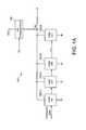
- FIG. 1Ais a block diagram of a CAM row
- FIG. 1Bis a circuit diagram of a quaternary (XY) CAM cell
- FIG. 1Cshows a truth table for data storage of the XY CAM cell of FIG. 1B ;
- FIG. 2is a block diagram of a CAM device within which the present embodiments may be implemented
- FIG. 3is a block diagram of one embodiment of the CAM array of FIG. 2 ;
- FIG. 4is a circuit diagram of a CAM row including a CAM cell configured in accordance with some embodiments
- FIG. 5Ais a timing diagram depicting a match condition in the CAM row of FIG. 4 ;
- FIG. 5Bis a timing diagram depicting a mismatch condition in the CAM row of FIG. 4 ;
- FIG. 6Ais a circuit diagram of a row including the CAM cell of FIG. 4 coupled to a match logic configured in accordance with some embodiments;
- FIG. 6Bis a circuit diagram of a portion of the match logic of FIG. 6A in accordance with some embodiments.
- FIG. 6Cis a circuit diagram of a CAM row including CAM cell of FIG. 4 coupled to match logic of FIG. 6A and to a second pre-charging circuit in accordance with some embodiments;
- FIG. 7is a circuit diagram of a CAM row including a CAM cell configured in accordance with other embodiments.
- FIG. 8Ais a timing diagram depicting a match condition in the CAM row of FIG. 7 ;
- FIG. 8Bis a timing diagram depicting a mismatch condition in the CAM row of FIG. 7 ;
- FIG. 9is a circuit diagram of a CAM row including a CAM cell and a match line charging circuit configured in accordance with another embodiment
- FIG. 10is a circuit diagram of a CAM row including a CAM cell and a match line charging circuit configured in accordance with yet another embodiment.
- FIG. 11is a circuit diagram of a CAM row including a CAM cell and a match line charging circuit configured in accordance with still another embodiment.
- FIG. 1Ashows a CAM row 100 as having a number of CAM cells 102 ( 1 )- 102 ( n ) each coupled to an associated match line ML.
- Each CAM cell 102is coupled between match line ML and ground potential.
- each CAM cell 102includes at least one storage element to store one or more data bits and includes at least one compare circuit that compares a bit of a search key (e.g., a comparand word) with data stored in the storage element.
- the storage elementcan be implemented using Static Random Access Memory (SRAM), Dynamic RAM (DRAM), a non-volatile memory cell (e.g., EEPROM or flash memory cell), or any other suitable memory element.
- SRAMStatic Random Access Memory
- DRAMDynamic RAM
- EEPROM or flash memory cellany other suitable memory element.
- word lines, bit lines, comparand lines, and other well-known elements of the associated CAM arrayare not shown in FIG. 1A .
- a match line charging circuit 106is coupled between a supply voltage VDD and match line ML, and includes an input to receive a pre-charge signal (PC).
- PCpre-charge signal
- match line MLPrior to each compare operation between an n-bit comparand word and an n-bit CAM word stored in CAM cells 102 ( 1 )- 102 ( n ), match line ML is pre-charged to VDD via match line charging circuit 106 in response to PC. Then, the n-bits of the comparand word are compared with corresponding bits of the CAM word in respective CAM cells 102 ( 1 )- 102 ( n ). If all bits of the comparand word match corresponding bits of the CAM word, then the match line ML remains in its charged state to indicate a match condition. Conversely, if one or more of the comparand bits do not match corresponding bits of the CAM word, then the one or more mismatching CAM cells 102 discharge match line ML low toward ground potential to indicate a mismatch condition.
- FIG. 1Bshows a quaternary CAM cell 110 .
- Quaternary CAM cell 110which is also referred to as an XY CAM cell, includes two storage cells 120 and 122 coupled to a compare circuit 130 , where the X cell 120 stores a first data bit X and the Y cell 122 stores a second data bit Y. More specifically, the two data bits X and Y can collectively represent four possible states: “0”, “1”, “don't care”, and a fourth state which may be left unused or may indicate “invalid,” as depicted in FIG. 1C .
- the logic “0” and “1” statescorrespond to the logic states represented, for example, by a conventional binary CAM cell.
- compare circuit 130For each of these states, if the comparand data (e.g., provided to CAM cell 110 via complementary comparand lines CL and CLB) matches the data stored in CAM cell 110 , compare circuit 130 does not discharge the match line ML, thereby indicating a match condition. Conversely, if the comparand data does not match the data stored in CAM cell 110 , compare circuit 130 discharges match line ML (e.g., toward ground potential) to indicate the mismatch condition. For the “don't care” state, the logic low values for X and Y maintain respective transistors 132 and 134 in non-conductive states, thereby preventing compare circuit 130 from discharging match line ML.
- match line MLe.g., toward ground potential
- the present embodimentsreduce power consumption of CAM devices during compare operations between a search key and data stored in the device's array by reducing the amount of electric charge by which the match line is discharged during mismatch conditions. More specifically, for some embodiments, respective rows (e.g., each row) of the CAM array includes circuitry that discharges the match line to a virtual ground line (e.g., rather than to ground potential) during mismatch conditions. Because the electrical potential on the virtual ground line is greater than ground potential, power consumption associated with pre-charging the match line back to a logic high state during the next compare operation is reduced, as compared to techniques that discharge the match line completely to ground potential.
- a virtual ground linee.g., rather than to ground potential
- the power terminal of a match detect circuitis connected to the virtual ground node instead of ground potential, which advantageously reduces undesirable crowbar currents in the match detect circuit.
- the CAM rowis modified to include a match line pre-charging circuit that utilizes a tank capacitor to increase the rate at which the match line can be charged.
- FIG. 2is a block diagram of a CAM device 200 within which the present embodiments can be implemented.
- CAM device 200includes a CAM array 210 , an address decoder 220 , a comparand register 230 , a read/write circuit 240 , a priority encoder circuit 250 , and match logic 260 .
- CAM array 210includes any number of rows of CAM cells (not shown for simplicity in FIG. 2 ), where each row of CAM cells can be configured to store a data word. Further, while CAM array 210 is shown in FIG. 2 as a single CAM array, it may include any number of CAM array blocks that can be independently searched.
- One or more instructions and related control signalsmay be provided to CAM device 200 from an instruction decoder (not shown for simplicity) to control read, write, compare, and other operations for CAM device 200 .
- Other well-known signals that can be provided to CAM device 200such as enable signals, clock signals, and power connections, are not shown for simplicity.
- each row of CAM cells in CAM array 210may have one or more validity bits to indicate whether the corresponding row (or any segment thereof) of CAM cells stores valid data.
- Each row of CAM cells (not shown in FIG. 2 for simplicity) in CAM array 210is coupled to address decoder 220 via a corresponding word line WL, and to priority encoder 250 and to well-known match logic 260 via a corresponding match line ML.
- the word lines and match linesare represented collectively in FIG. 2 .
- Address decoder 220is well-known, and includes circuitry to select corresponding rows in CAM array 210 for read, write, and/or other operations in response to an address received from an address bus ABUS using the word lines WL.
- addressesmay be provided to address decoder 220 from another suitable bus and/or circuitry.
- the match lines MLprovide match results for compare operations between comparand data (e.g., a search key) and data stored in CAM array 210 .
- Priority encoder 250uses the match results indicated on the match lines to determine the matching entry that has the highest priority number associated with it and generates the index or address of this highest priority match (HPM).
- priority encoder 250may use the validity bits from CAM array 210 to generate the next free address that is available in CAM array 210 for storing new data.
- priority encoder 250may provide the next free address to the address decoder 220 .
- Match logic 260uses the match results indicated on the match lines to generate a match flag (MF) indicative of a match condition in CAM array 210 . If there is more than one matching entry in CAM array 210 , match logic 260 may generate a multiple match flag to indicate a multiple match condition. In addition, match logic 260 may use the validity bits from CAM array 210 to assert a full flag when all of the rows of CAM cells in CAM array 210 are filled with valid entries.
- MFmatch flag
- Each column of CAM cells (not shown in FIG. 2 for simplicity) in CAM array 210is coupled to comparand register 230 via one or more corresponding comparand lines CL, and is coupled to read/write circuit 240 via one or more corresponding bit lines BL.
- the comparand lines CL and bit lines BLare represented collectively in FIG. 2 .
- Comparand register 230is well-known, and is configured to provide a search key (e.g., a comparand word) received from a comparand bus CBUS to CAM array 210 during compare operations with data stored therein.
- the search keycan be provided to CAM array 210 via another bus and/or circuit.
- Read/write circuit 240includes well-known write drivers to write data received from a data bus DBUS to CAM array 210 via the bit lines BL, and includes well-known sense amplifiers to read data from CAM array 210 onto DBUS.
- read/write circuit 240may be coupled to a bus other than DBUS.
- CAM device 200can include a well-known global mask circuit (e.g., coupled to the comparand register 230 ) that can selectively mask the bits of the search key provided to the CAM array 210 .
- FIG. 3is a more detailed block diagram of one embodiment of CAM array 210 of FIG. 2 .
- CAM array 210is shown to include a plurality of CAM cells 302 (e.g., including cells 102 ( 1 )- 102 ( n ), FIG. 1A ) organized in any number of rows and columns.
- the CAM cells 302can be any suitable type of CAM cell including, for example, binary CAM cells, ternary CAM cells, and/or quaternary CAM cells (e.g., quaternary CAM cells 110 , FIG. 1B ).
- each row of CAM array 210may also include one or more validity bits.
- Each row of CAM cells 302is coupled to a match line ML and to a word line WL.
- Each word line WLis driven by address decoder 220 to select one or more rows of CAM cells 302 for writing or reading.
- Each match line MLis coupled to priority encoder 250 via a corresponding match detect circuit 312 .
- the match detect circuits 312are clocked by a match detect clock signal CLK_DET in a well-known manner.
- Each column of CAM cells 302 in CAM array 210is coupled to read/write circuit 240 via a complementary bit line pair BL/BLB, and to comparand register 230 via a complementary comparand line pair CL/CLB.
- the match lines MLPrior to compare operations, the match lines ML are pre-charged (e.g., to logic high), and each set of complementary comparand line pairs CL/CLB are driven to the same predetermined logic level (e.g., to logic low). Then, during compare operations, the comparand register 230 provides the search key (e.g., the comparand word) to the CAM cells 302 by driving each pair of complementary comparand lines CL/CLB to opposite logic states indicative of the corresponding bit of the search key.
- the search keye.g., the comparand word
- the corresponding comparand line CLis driven to a logic low state and the corresponding complementary comparand line CLB is driven to a logic high state; conversely, to provide a logic high comparand bit C to the column of CAM cells, the corresponding comparand line CL is driven to the logic high state and the corresponding complementary comparand line CLB is driven to the logic low state. Thereafter, if the data bits in all the CAM cells 302 in a particular row match the corresponding bits of the search key, then the match line ML remains in its pre-charged (e.g., logic high) state to indicate the match condition.
- pre-chargede.g., logic high
- mismatching CAM cells 302discharge the match line (e.g., toward ground potential) to indicate the mismatch condition.
- FIG. 4shows a CAM row 400 in accordance with some of the present embodiments.
- CAM row 400which can be deployed in CAM arrays of the type described above with respect to FIGS. 2-3 , is shown to include a PMOS match line pre-charge transistor 410 , a CAM cell 420 , a match line ML, a virtual-ground line (VGL), an NMOS discharge transistor 440 , and a match detect circuit 450 .
- CAM row 400can have any number of CAM cells 420 .
- the CAM cell 420is shown as a quaternary CAM cell, in alternate embodiments the CAM cell 420 is another type of CAM cell (e.g., a binary or ternary CAM cell).
- Pre-charge transistor 410is connected between the supply voltage VDD and match line ML, and has a gate to receive a complemented pre-charge signal PC .
- Compare circuit 430which is connected between match line ML and the virtual-ground line (VGL), includes two parallel discharge paths between match line ML and virtual-ground line VGL.
- One pathincludes series-connected transistors 431 and 432 having respective gate terminals to receive a comparand bit from comparand line CL and to receive the data bit X, and the other path includes series-connected transistors 433 and 434 having respective gate terminals to receive a complimentary comparand bit from complementary comparand line CLB and to receive the data bit Y.
- NMOS discharge transistor 440is connected between VGL and ground potential, and has a gate to receive the pre-charge signal PC. In this manner, compare circuit 430 and virtual-ground line VGL are selectively connected to ground potential by discharge transistor 440 in response to pre-charge signal PC. This is in contrast to CAM row and cell architectures in which the compare circuit is directly connected to ground potential, for example, as for CAM cell 110 of FIG. 1B .
- Match detect circuit 450includes a NAND gate 452 and a CMOS inverter 454 .
- NAND gate 452which is well-known, has a first input coupled to match line ML, a second input to receive a match detect clock signal CLK_DET, and an output coupled to the input of inverter 454 .
- the output of inverter 454provides a latched match line (LML) signal.
- LMLlatched match line
- the pre-charge signal PCis asserted (e.g., to logic high).
- discharge transistor 440turns on and discharges the virtual-ground line VGL low to ground potential.
- the resulting logic low state of PCturns on pre-charge transistor 410 , which pre-charges the match line ML high towards VDD.
- the comparand lines CL/CLBare both pre-charged to logic low during the pre-charge phase of the compare operation.
- the pre-charge signal PCis de-asserted (e.g., to logic low)
- the complementary comparand bitsare provided to the gates of transistors 431 and 433 via comparand lines CL and CLB, respectively, and CLK_DET is asserted (e.g., to logic high).
- the de-asserted state of PCturns off discharge transistor 440 to isolate the VGL from ground potential.
- the resulting logic high state of PCturns off pre-charge transistor 410 . If the comparand bit matches the data value stored in CAM cell 420 , then compare circuit 430 is non-conductive and isolates match line ML from the VGL, thereby allowing match line ML to remain in its pre-charged logic high state to indicate the match condition.
- both match line ML and the virtual-ground line VGLsubstantially maintain their respective high and low voltage levels.
- the logic high state of the match line MLis detected by match detect circuit 450 in response to CLK_DET, and then provided as a logic high output signal.
- compare circuit 430turns on and connects the match line ML to the VGL, thereby allowing match line ML to discharge to the VGL.
- the resulting logic low state of match line MLis detected by match detect circuit 450 in response to CLK_DET, and then provided as a logic low output signal.
- match detect circuit 450in response to CLK_DET, and then provided as a logic low output signal.
- match line MLdischarges to the VGL
- the VGLslowly charges towards the voltage level of match line ML.
- the voltage levels of match line ML and the VGLconverge to substantially the same voltage level during mismatch conditions (e.g., as discussed in more detail below with respect to FIG. 5B ).
- assertion of PCturns on discharge transistor 440 , which discharges any residual charge on the VGL to ground potential.
- Turning off discharge transistor 440 during the evaluation phase of the compare operationnot only prevents a DC path between the match line ML and ground potential, but also prevents match line ML from being completely discharged to ground potential during mismatch conditions.
- the match line MLcan be more easily pre-charged towards VDD by pre-charge transistor 410 during the pre-charge phase of the next compare operation, thereby reducing power consumption (e.g., as compared to CAM rows in which the match line ML is completely discharged to ground potential during mismatch conditions).
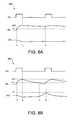
- FIG. 5Ais a timing diagram 500 depicting various signal and line voltages corresponding to a match condition in CAM cell 420 of FIG. 4 .
- the pre-charge signal PCis asserted to logic high (and thus PC is asserted to logic low).
- PMOS pre-charge transistor 410turns on and charges match line ML high towards VDD
- NMOS discharge transistor 440turns on and discharges the VGL low to ground potential.
- the pre-charge signal PCis de-asserted to logic low (and thus PC is de-asserted to logic high).
- PMOS pre-charge transistor 410turns off and isolates match line ML from VDD
- NMOS discharge transistor 440turns off and isolates the VGL from ground potential. Because the comparand bit matches the data stored in CAM cell 420 , compare circuit 430 does not connect the match line ML to the VGL, thereby allowing the match line ML to remain in its charged logic high state and allowing the VGL to remain close to ground potential. As a result, the differential voltage between match line ML and the VGL is approximately equal to VDD during match conditions.
- FIG. 5Bis a timing diagram 550 depicting signals corresponding to a mismatch condition in CAM cell 420 of FIG. 4 .
- the match line ML voltageis charged towards VDD and the VGL voltage is discharged towards ground potential in response to assertion of PC.
- compare circuit 430 of CAM cell 420discharges the match line ML low towards the VGL, which is isolated from ground potential by the non-conductive state of discharge transistor 440 (e.g., in response to de-assertion of PC).
- the CAM row and cell architecture of FIG. 4can improve noise margin and reduce power consumption, as compared to CAM row and cell architectures discussed above with respect to FIG. 1B .
- the resulting intermediate voltage on match line ML during mismatch conditionscan undesirably lead to crowbar currents in match detect circuit 450 .
- the match line voltageis equal to the intermediate voltage (Vint) following a mismatch condition
- the associated NMOS pull-down transistor(not shown for simplicity) within NAND gate 452 that is driven by the match line ML may not completely turn off, thereby resulting in undesirable crowbar currents through NAND gate 452 .
- the ground terminal of the match detect circuitcan be connected to the VGL instead of ground potential, as discussed below with respect to FIG. 6A .
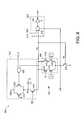
- FIG. 6Ais a circuit diagram of a CAM row 600 including CAM cell 420 of FIG. 4 coupled to a match detect circuit 610 configured in accordance with some embodiments.
- CAM row 600which can be deployed in CAM arrays of the type described above with respect to FIGS. 2-3 , is shown to include PMOS match line pre-charge transistor 410 , CAM cell 420 , NMOS discharge transistor 440 , match line ML, the VGL, and match detect circuit 610 .
- PMOS match line pre-charge transistor 410for example, CAM cell 420 is depicted in CAM row 600 .
- CAM row 600can have any number of CAM cells 420 .
- only the X and Y storage cells and compare circuit 430are shown in FIG. 6A .
- CAM row 600is similar to CAM row 400 of FIG. 4 , except that the ground terminal of match detect circuit 610 is connected to the VGL instead of ground potential. Connecting the ground terminal of match detect circuit 610 to the VGL instead of ground potential allows the gate-to-source voltage (V GS ) of the NAND gate's NMOS pull-down transistor (not shown in FIG. 6A for simplicity) to be almost zero during a mismatch condition, which in turn advantageously reduces the crowbar current of NAND gate 452 . Further, connecting the ground terminal of match detect circuit 610 to the VGL instead of ground potential improves the noise margin of match detect circuit 610 by altering the trip point that distinguishes detection of match and mismatch conditions.
- V GSgate-to-source voltage
- FIG. 6Bshows a circuit diagram of a NAND gate 605 that is one embodiment of NAND gate 452 of FIG. 6A .
- NAND gate 605includes two PMOS transistors MP 1 -MP 2 and two NMOS transistors MN 1 -MN 2 .
- PMOS transistor MP 1is connected between VDD and an output terminal (OUT) of NAND gate 605 , and has a gate coupled to match line ML.
- PMOS transistor MP 2is connected between VDD and OUT, and has a gate to receive CLK_DET.
- NMOS transistors MN 1 and MN 2are connected in series between OUT and the VGL, with the gate of transistor MN 1 to receive CLK_DET and the gate of transistor MN 2 coupled to match line ML.
- NAND gate 605has power terminals connected to VDD and to the VGL, rather than to VDD and to ground potential.
- the match line voltage and the VGL voltageare both approximately equal to the intermediate voltage (Vint) following a mismatch condition (see also FIG. 5B )
- the gate and source voltages of transistor MN 2are also both approximately equal to Vint.
- the V GS of transistor MN 2is approximately zero during the mismatch condition, thereby desirably maintaining transistor MN 2 in a non-conductive state and significantly reducing the crowbar current.
- FIG. 6Cis a circuit diagram of a CAM row 601 having CAM cell 420 of FIG. 4 coupled to match detect circuit 610 .
- CAM row 601which can be deployed in CAM arrays of the type described above with respect to FIGS. 2-3 , is shown to include pre-charge transistor 410 , CAM cell 420 , NMOS discharge transistor 440 , the VGL, match line ML, match detect circuit 610 , and a match line keeper circuit 620 .
- pre-charge transistor 410CAM cell 420
- NMOS discharge transistor 440the VGL, match line ML, match detect circuit 610
- a match line keeper circuit 620For simplicity, only one CAM cell 420 is depicted in CAM row 601 .
- CAM row 601can have any number of CAM cells 420 . Further, for simplicity, only the X and Y storage cells and compare circuit 430 of CAM cell 420 are shown in FIG. 6C .
- CAM row 601is similar to CAM row 600 of FIG. 6A , except that CAM row 601 also includes match line keeper circuit 620 connected between VDD and the match line ML.
- Keeper circuit 620which includes a PMOS transistor 622 and a NAND gate 624 , acts as a keeper circuit to compensate for leakage currents associated with CAM cell 420 .
- PMOS transistor 622is connected between VDD and match line ML, and has a gate coupled to an output of NAND gate 624 .
- a first input of NAND gate 624is connected to match line ML, and a second input of NAND gate 624 is coupled to receive a pre-charge clock signal PCLK.
- the pre-charge signal PCis asserted to logic high (and thus PC is asserted to logic low).
- PMOS pre-charge transistor 410turns on and charges match line ML high towards VDD
- NMOS discharge transistor 440turns on and discharges the VGL low to ground potential.
- the pre-charge signal PCis de-asserted to logic low (and thus PC is de-asserted to logic high).
- PMOS pre-charge transistor 410turns off and isolates match line ML from VDD
- NMOS discharge transistor 440turns off and isolates the VGL from ground potential.
- PCLKis asserted to logic high during the evaluation phase to allow NAND gate 624 to turn on PMOS pull-up transistor 622 if the match line ML is in a charged logic high state.
- compare circuit 430does not connect the match line ML to the VGL, thereby allowing the match line ML to remain in its charged logic high state and allowing the VGL to remain close to ground potential.
- the logic high state of match line MLforces the output of NAND gate 624 to logic low, thereby turning on PMOS pull-up transistor 622 to charge match line ML towards VDD. In this manner, PMOS transistor 622 and NAND gate 624 together act as a keeper circuit to maintain match line ML in its charged logic high state.
- compare circuit 430discharges the match line ML to the VGL (e.g., in a manner similar to that described above with respect to FIG. 5B ).
- the resulting logic low state of match line MLforces the output of NAND gate 624 to logic high, thereby turning off PMOS pull-up transistor 622 and isolating match line ML from VDD.
- FIG. 7is a circuit diagram of a CAM row 700 including CAM cell 420 of FIG. 4 coupled to match detect circuit 610 configured in accordance with some embodiments.
- CAM row 700which can be deployed in CAM arrays of the type described above with respect to FIGS. 2-3 , is shown to include PMOS match line pre-charge transistor 410 , CAM cell 420 , NMOS discharge transistor 440 , the VGL, match line ML, and match detect circuit 610 .
- PMOS match line pre-charge transistor 410for example, CAM cell 420 is depicted in CAM row 700 .
- CAM row 700can have any number of CAM cells 420 .
- row 700can include the match line keeper circuit 620 of FIG. 6C .
- CAM row 700is similar to CAM row 600 of FIG. 6A , except that the gate of NMOS discharge transistor 440 is connected to match line ML instead of receiving the pre-charge signal PC. Connecting the gate of discharge transistor 440 to match line ML rather than the PC signal can reduce power consumption by limiting the minimum voltage of match line ML during mismatch conditions to the threshold voltage (VT) of NMOS discharge transistor 440 (e.g., rather than to ground potential).
- VTthreshold voltage
- FIG. 8Ais a timing diagram 800 depicting various signal and line voltages corresponding to a match condition in the embodiment of FIG. 7 .
- the PC signalis asserted (e.g., to logic high) so that PMOS pre-charge transistor 410 pulls match line ML high towards VDD.
- the logic high voltage on match line MLturns on NMOS discharge transistor 440 , which discharges the VGL to ground potential.
- the comparand lines CL/CLBare both pre-charged to logic low during the pre-charge phase of the compare operation.
- compare circuit 430is non-conductive in response to the match condition, and match line ML remains in its charged logic high state (e.g., at approximately VDD).
- the resulting logic high state of match line MLmaintains NMOS discharge transistor 440 in a conductive state, thereby maintaining the VGL at ground potential.
- the match line voltagecan slightly discharge because of leakage currents in compare circuit 430
- the conductive state of NMOS discharge transistor 440prevents charge from undesirably accumulating on the VGL.
- FIG. 8Bis a timing diagram 850 depicting various signal and line voltages corresponding to a mismatch condition in the embodiment of FIG. 7 .
- the pre-charge phaseis similar to that described above with respect to FIG. 8A .
- compare circuit 430is conductive in response to the mismatch condition, and discharges the match line ML low towards ground potential.
- VTthreshold voltage
- discharge transistor 440turns off and de-couples the VGL from ground potential, thereby preventing match line ML from completely discharging to ground potential.
- match line MLcan be pre-charged to its logic high state (e.g., towards VDD) for the next compare operation using less current than CAM row architectures of the type depicted in FIG. 1B .
- FIG. 9is a circuit diagram of a CAM row 900 in accordance with other embodiments that utilize charge sharing for match line ML.
- CAM row 900is similar to CAM row 700 of FIG. 7 , except that pre-charge transistor 410 is replaced by a match line charging circuit 910 .
- charging circuit 910includes PMOS transistors 622 , 914 , and 916 , NAND gate 624 , and a tank capacitor C 1 .
- PMOS transistors 914 and 622are connected in parallel between VDD and a charging node N 1 , with the gate of PMOS transistor 914 coupled to ground potential and the gate of PMOS transistor 622 coupled to the output of NAND gate 624 .
- PMOS transistor 914is maintained in a conductive state, and PMOS transistor 622 is responsive to a logical combination of the match signal on match line ML and PCLK (e.g., in a manner similar to that described above with respect to FIG. 6C ).
- a strong PMOS transistor 916is connected between node N 1 and match line ML, and is responsive to PC.
- Tank capacitor C 1which is connected between node N 1 and ground potential, is continuously charged towards VDD by a weak PMOS transistor 914 , and is also selectively charged towards VDD by PMOS transistor 622 (e.g., when PCLK is asserted high and match line ML is in its charged logic high state).
- PMOS transistor 622 and NAND gate 624which together form a match line keeper circuit, can be omitted.
- PCis asserted to logic high (and thus PC is logic low), which turns on PMOS transistor 916 and thereby connects node N 1 to match line ML.
- PCis asserted to logic high (and thus PC is logic low), which turns on PMOS transistor 916 and thereby connects node N 1 to match line ML.
- most of the charge stored on the tank capacitor C 1is shared with match line ML, thereby quickly charging match line ML high to a maximum level VDD/2 if the capacitance of match line ML and tank capacitor C 1 are the same.
- the match line MLis also charged by the weak PMOS pull-up transistor 914 , thereby increasing the voltage level of match line ML. Note that the voltage level of the charged match line ML can be controlled by adjusting the size and/or gate voltage of PMOS transistor 914 .
- the comparand lines CL and CLBneed not be driven to the low logic state because the match line is being charged primarily through the tank capacitor C 1 and not through a bulky PMOS transistor, which can reduce power consumption. This is in contrast to previous embodiments described above with respect to FIGS. 4 , 6 A, 6 C, and 7 .
- PCis de-asserted to logic low (and thus PC is logic high) and turns off PMOS transistor 916 , thereby isolating node N 1 from match line ML.
- the tank capacitor C 1continues to be charged by the weak PMOS pull-up transistor 914 during the evaluation phase.
- compare circuit 430If there is a match condition, compare circuit 430 is non-conductive, thereby allowing match line ML to be charged to approximately VDD/2. As the match line voltage increases above the threshold voltage (Vtn) of transistor 440 , NMOS discharge transistor 440 turns on and discharges the VGL to ground potential. The logic high state of match line ML also forces the output of NAND gate 624 to logic low, thereby turning on PMOS pull-up transistor 622 to further charge match line ML towards VDD. Conversely, if there is a mismatch condition, compare circuit 430 is conductive and discharges match line ML low towards the VGL.
- match line MLAs the voltage on match line ML falls below the Vtn of discharge transistor 440 , discharge transistor 440 turns off and de-couples the VGL from ground potential, thereby preventing match line ML from completely discharging to ground potential. Thus, the match line ML discharges to the VGL, which in turn experiences an increase in voltage to the Vt of transistor 440 .
- FIG. 10is a circuit diagram of a CAM row 1000 in accordance with other embodiments.
- CAM row 1000is similar to CAM row 900 of FIG. 9 , except that CAM row 1000 includes a match line charging circuit 1010 and a diode-connected NMOS transistor 1020 .
- Diode-connected NMOS transistor 1020is connected between the VGL and ground potential, and effectively clamps the VGL voltage at the VT of NMOS transistor 1020 . Without diode 1020 , the voltage on the VGL can reach undesirably high levels during mismatch conditions because, as discussed above with respect to FIG. 9 , the VGL is charged by both the discharging match line ML and the tank capacitor C 1 if there is a mismatch condition.
- Charging circuit 1010includes PMOS transistor 914 , PMOS transistor 916 , and tank capacitor C 1 of FIG. 9 , plus an additional PMOS pull-up transistor 1012 connected in parallel with PMOS transistors 914 and 916 . More specifically, PMOS transistor 1012 is connected between VDD and match line ML, and has a gate connected to the VGL. In this manner, PMOS pull-up transistor 1012 turns on and charges match line ML high towards VDD sooner than does PMOS pull-up transistor 622 of FIG. 9 , as described in more detail below.
- PCis asserted to logic high (and thus PC is logic low), which turns on PMOS transistor 916 and thereby connects node N 1 to match line ML.
- most of the charge stored on the tank capacitor C 1is shared with match line ML, thereby quickly charging match line ML high towards VDD.
- the match line MLis also charged by the weak pull-up PMOS transistor 914 , thereby increasing the voltage level of match line ML.
- PCis de-asserted to logic low and turns off PMOS transistor 916 , thereby isolating node N 1 from match line ML.
- the tank capacitor C 1continues to be charged by PMOS transistor 914 during the evaluation phase.
- match line MLcharges to approximately VDD/2 due to the charge from tank capacitor C 1 .
- the size of the weak PMOS transistor 914is configurable to raise the voltage of match line ML even further to a desired level across various process corners. As the match line voltage exceeds the Vtn of transistor 440 , NMOS discharge transistor 440 turns on and discharges the VGL to ground potential. As the VGL voltage falls below the Vtp of PMOS transistor 1012 , PMOS transistor 1012 turns on and charges the match line ML higher towards VDD.
- the advantage of having this weak keeper circuit over the scheme of FIG. 9is reduction in area and no crowbar current of NAND gate 624 .
- compare circuit 430is conductive and discharges match line ML low towards the VGL.
- discharge transistor 440turns off and de-couples the VGL from ground potential, thereby preventing match line ML from completely discharging to ground potential.
- the match line MLdischarges to the VGL, which in turn experiences an increase in voltage not only from the discharging match line ML but also from the discharging of the tank capacitor.
- the increasing voltage on the VGLmaintains PMOS pull-up transistor 1012 in a non-conductive state. As noted above, however, the VGL voltage is clamped at Vtn by diode-connected transistor 1020 .
- leakage currents during compare idle timescan inadvertently turn on the PMOS pull-up transistor 1012 .
- the VGLwill slowly discharge through diode 1020 and NMOS discharge transistor 440 .
- the decreasing VGL voltageslowly turns on the PMOS pull-up transistor 1012 , which in turn undesirably starts to charge the match line ML high towards VDD.
- the PMOS pull-up transistor 1012remains conductive and continues to charge the match line ML, even during idle cycles, which can undesirably increase power consumption.
- FIG. 11is a circuit diagram of a CAM row 1100 configured to address leakage problems discussed above with respect to FIG. 10 .
- CAM row 1100is similar to CAM row 1000 of FIG. 10 , except that CAM row 1100 includes a match line charging circuit 1110 .
- Charging circuit 1110is similar to charging circuit 1010 of FIG. 10 , with the addition of a PMOS pull-up transistor 1114 connected in series between VDD and PMOS pull-up transistor 1012 .
- the gate of PMOS pull-up transistor 1114receives an active low compare signal CMP that is asserted to logic low only during the compare operation. Thus, during idle cycles, CMP is asserted to logic high to turn off PMOS pull-up transistor 1114 , which reduces power consumption during the idle cycles.
- circuits disclosed hereinmay be described using computer aided design tools and expressed (or represented), as data and/or instructions embodied in various computer-readable media, in terms of their behavioral, register transfer, logic component, transistor, layout geometries, and/or other characteristics. Formats of files and other objects in which such circuit expressions may be implemented include, but are not limited to, formats supporting behavioral languages such as C, Verilog, and VHDL, formats supporting register level description languages like RTL, and formats supporting geometry description languages such as GDSII, GDSIII, GDSIV, CIF, MEBES and any other suitable formats and languages.
- Non-transitory computer-readable media in which such formatted data and/or instructions may be embodiedinclude, but are not limited to, non-volatile storage media in various forms (e.g., optical, magnetic or semiconductor storage media).
Landscapes
- Semiconductor Integrated Circuits (AREA)
Abstract
Description
Claims (35)
Priority Applications (1)
| Application Number | Priority Date | Filing Date | Title |
|---|---|---|---|
| US13/167,552US8837188B1 (en) | 2011-06-23 | 2011-06-23 | Content addressable memory row having virtual ground and charge sharing |
Applications Claiming Priority (1)
| Application Number | Priority Date | Filing Date | Title |
|---|---|---|---|
| US13/167,552US8837188B1 (en) | 2011-06-23 | 2011-06-23 | Content addressable memory row having virtual ground and charge sharing |
Publications (1)
| Publication Number | Publication Date |
|---|---|
| US8837188B1true US8837188B1 (en) | 2014-09-16 |
Family
ID=51493425
Family Applications (1)
| Application Number | Title | Priority Date | Filing Date |
|---|---|---|---|
| US13/167,552Active2031-06-30US8837188B1 (en) | 2011-06-23 | 2011-06-23 | Content addressable memory row having virtual ground and charge sharing |
Country Status (1)
| Country | Link |
|---|---|
| US (1) | US8837188B1 (en) |
Cited By (7)
| Publication number | Priority date | Publication date | Assignee | Title |
|---|---|---|---|---|
| US20160148689A1 (en)* | 2014-11-26 | 2016-05-26 | Invecas, Inc. | Sense Amplifier for Single-ended Sensing |
| WO2016123731A1 (en)* | 2015-02-02 | 2016-08-11 | Micron Technology, Inc. | Apparatuses and methods for transistor protection by charge sharing |
| TWI579860B (en)* | 2015-03-23 | 2017-04-21 | 國立成功大學 | A memory cell and a content addressable memory with the memory cell |
| US20170140822A1 (en)* | 2015-11-12 | 2017-05-18 | Mediatek Inc. | Sense amplifier circuits |
| US9947406B2 (en)* | 2015-02-23 | 2018-04-17 | Qualcomm Incorporated | Dynamic tag compare circuits employing P-type field-effect transistor (PFET)-dominant evaluation circuits for reduced evaluation time, and related systems and methods |
| US20190164608A1 (en)* | 2017-11-29 | 2019-05-30 | Renesas Electronics Corporation | Semiconductor device |
| US20210295885A1 (en)* | 2020-03-23 | 2021-09-23 | Mediatek Singapore Pte. Ltd. | Simultaneous write and search operation in a content addressable memory |
Citations (128)
| Publication number | Priority date | Publication date | Assignee | Title |
|---|---|---|---|---|
| US3665422A (en) | 1970-01-26 | 1972-05-23 | Electronic Arrays | Integrated circuit,random access memory |
| US4112502A (en) | 1976-10-18 | 1978-09-05 | Sperry Rand Corporation | Conditional bypass of error correction for dual memory access time selection |
| US4747080A (en) | 1985-11-12 | 1988-05-24 | Nippon Telegraph & Telephone Corporation | Semiconductor memory having self correction function |
| US4779226A (en) | 1985-05-10 | 1988-10-18 | Haraszti Tegze P | Complementary high performance cam cell |
| US4791606A (en) | 1987-09-01 | 1988-12-13 | Triad Semiconductors International Bv | High density CMOS dynamic CAM cell |
| US4831585A (en) | 1985-11-27 | 1989-05-16 | Massachusetts Institute Of Technology | Four transistor cross-coupled bitline content addressable memory |
| US4903268A (en) | 1985-09-26 | 1990-02-20 | Mitsubishi Denki Kabushiki Kaisha | Semiconductor memory device having on-chip error check and correction functions |
| US4958352A (en) | 1987-10-05 | 1990-09-18 | Mitsubishi Denki Kabushiki Kaisha | Semiconductor memory device with error check and correcting function |
| US4991136A (en) | 1988-01-29 | 1991-02-05 | Mitsubishi Denki Kabushiki Kaisha | Semiconductor associative memory device with memory refresh during match and read operations |
| US5046046A (en) | 1978-03-10 | 1991-09-03 | Intel Corporation | Redundancy CAM using word line from memory |
| US5073727A (en) | 1988-06-17 | 1991-12-17 | Harumi Shizu | Cmos inverter with noise reduction feedback means |
| US5127014A (en) | 1990-02-13 | 1992-06-30 | Hewlett-Packard Company | Dram on-chip error correction/detection |
| US5184325A (en) | 1989-03-10 | 1993-02-02 | Board Of Regents, The University Of Texas System | Dynamic associative memory with logic-in-refresh |
| US5233614A (en) | 1991-01-07 | 1993-08-03 | International Business Machines Corporation | Fault mapping apparatus for memory |
| US5311462A (en) | 1991-12-19 | 1994-05-10 | Intel Corporation | Physical placement of content addressable memories |
| US5319590A (en) | 1992-12-04 | 1994-06-07 | Hal Computer Systems, Inc. | Apparatus for storing "Don't Care" in a content addressable memory cell |
| US5319589A (en) | 1992-04-17 | 1994-06-07 | Mitsubishi Denki Kabushiki Kaisha | Dynamic content addressable memory device and a method of operating thereof |
| US5450424A (en) | 1992-07-27 | 1995-09-12 | Mitsubishi Denki Kabushiki Kaisha | Semiconductor memory device with error checking and correcting function |
| US5452243A (en) | 1994-07-27 | 1995-09-19 | Cypress Semiconductor Corporation | Fully static CAM cells with low write power and methods of matching and writing to the same |
| US5455834A (en) | 1993-06-14 | 1995-10-03 | Hal Computer Systems, Inc. | Fault tolerant address translation method and system |
| US5469450A (en) | 1992-07-30 | 1995-11-21 | Samsung Electronics Co., Ltd. | Nonvolatile memory device including multi-ECC circuit |
| US5491703A (en) | 1992-06-30 | 1996-02-13 | Sgs-Thomson Microelectronics Ltd. | Cam with additional row cells connected to match line |
| US5561429A (en) | 1986-04-16 | 1996-10-01 | Raytheon Company | Content limit addressable memory |
| US5568415A (en) | 1993-02-19 | 1996-10-22 | Digital Equipment Corporation | Content addressable memory having a pair of memory cells storing don't care states for address translation |
| US5570377A (en) | 1992-11-30 | 1996-10-29 | Alcatel N.V. | Method and device for detection and correction of errors in ATM cell headers |
| US5572460A (en) | 1993-10-26 | 1996-11-05 | Integrated Device Technology, Inc. | Static random-access memory cell with capacitive coupling to reduce sensitivity to radiation |
| US5598115A (en) | 1993-02-23 | 1997-01-28 | Intergraph Corporation | Comparator cell for use in a content addressable memory |
| US5604753A (en) | 1994-01-04 | 1997-02-18 | Intel Corporation | Method and apparatus for performing error correction on data from an external memory |
| US5629950A (en) | 1992-04-24 | 1997-05-13 | Digital Equipment Corporation | Fault management scheme for a cache memory |
| US5642320A (en) | 1994-07-11 | 1997-06-24 | Hyundai Electronics Industries Co., Ltd. | Self-refreshable dual port dynamic CAM cell and dynamic CAM cell array refreshing circuit |
| US5644583A (en) | 1992-09-22 | 1997-07-01 | International Business Machines Corporation | Soft error correction technique and system for odd weight row error correction codes |
| US5682394A (en) | 1989-03-10 | 1997-10-28 | International Business Machines Corporation | Fault tolerant computer memory systems and components employing dual level error correction and detection with disablement feature |
| US5699369A (en) | 1995-03-29 | 1997-12-16 | Network Systems Corporation | Adaptive forward error correction system and method |
| US5727003A (en) | 1995-07-03 | 1998-03-10 | Cirrus Logic, Inc. | Method and apparatus for flash burst error correction |
| US5761222A (en) | 1994-09-30 | 1998-06-02 | Sgs-Thomson Microelectronics, S.R.L. | Memory device having error detection and correction function, and methods for reading, writing and erasing the memory device |
| US5796758A (en) | 1996-10-08 | 1998-08-18 | International Business Machines Corporation | Self-checking content-addressable memory and method of operation for detecting multiple selected word lines |
| US5796671A (en) | 1996-03-01 | 1998-08-18 | Wahlstrom; Sven E. | Dynamic random access memory |
| US5872802A (en) | 1996-05-03 | 1999-02-16 | Cypress Semiconductor Corp. | Parity generation and check circuit and method in read data path |
| US6009548A (en) | 1997-12-03 | 1999-12-28 | International Business Machines Corporation | Error correcting code retrofit method and apparatus for multiple memory configurations |
| US6032214A (en) | 1990-04-18 | 2000-02-29 | Rambus Inc. | Method of operating a synchronous memory device having a variable data output length |
| US6058500A (en) | 1998-01-20 | 2000-05-02 | 3Com Corporation | High-speed syndrome calculation |
| US6067656A (en) | 1997-12-05 | 2000-05-23 | Intel Corporation | Method and apparatus for detecting soft errors in content addressable memory arrays |
| US6125049A (en) | 1999-01-05 | 2000-09-26 | Netlogic Microsystems, Inc. | Match line control circuit for content addressable memory |
| US6128207A (en) | 1998-11-02 | 2000-10-03 | Integrated Device Technology, Inc. | Low-power content addressable memory cell |
| US6134631A (en) | 1996-08-19 | 2000-10-17 | Hyundai Electronics America, Inc. | Non-volatile memory with embedded programmable controller |
| US6137707A (en) | 1999-03-26 | 2000-10-24 | Netlogic Microsystems | Method and apparatus for simultaneously performing a plurality of compare operations in content addressable memory device |
| US6151247A (en) | 1997-03-31 | 2000-11-21 | Lexar Media, Inc. | Method and apparatus for decreasing block write operation times performed on nonvolatile memory |
| US6154384A (en) | 1999-11-12 | 2000-11-28 | Netlogic Microsystems, Inc. | Ternary content addressable memory cell |
| US6166939A (en) | 1999-07-12 | 2000-12-26 | Net Logic Microsystems | Method and apparatus for selective match line pre-charging in a content addressable memory |
| US6188629B1 (en) | 1999-11-05 | 2001-02-13 | Cecil H. Kaplinsky | Low power, static content addressable memory |
| US6191969B1 (en) | 1999-09-09 | 2001-02-20 | Net Logic Microsystems, Inc. | Selective match line discharging in a partitioned content addressable memory array |
| US6199140B1 (en) | 1997-10-30 | 2001-03-06 | Netlogic Microsystems, Inc. | Multiport content addressable memory device and timing signals |
| US6216246B1 (en) | 1996-05-24 | 2001-04-10 | Jeng-Jye Shau | Methods to make DRAM fully compatible with SRAM using error correction code (ECC) mechanism |
| US6233717B1 (en) | 1997-12-31 | 2001-05-15 | Samsung Electronics Co., Ltd. | Multi-bit memory device having error check and correction circuit and method for checking and correcting data errors therein |
| US6243281B1 (en) | 2000-06-14 | 2001-06-05 | Netlogic Microsystems, Inc. | Method and apparatus for accessing a segment of CAM cells in an intra-row configurable CAM system |
| US6243280B1 (en) | 1999-09-09 | 2001-06-05 | Netlogic Microsystems, Inc. | Selective match line pre-charging in a partitioned content addressable memory array |
| US6262907B1 (en) | 2000-05-18 | 2001-07-17 | Integrated Device Technology, Inc. | Ternary CAM array |
| US6289471B1 (en) | 1991-09-27 | 2001-09-11 | Emc Corporation | Storage device array architecture with solid-state redundancy unit |
| US6324087B1 (en) | 2000-06-08 | 2001-11-27 | Netlogic Microsystems, Inc. | Method and apparatus for partitioning a content addressable memory device |
| US6362990B1 (en) | 1999-09-10 | 2002-03-26 | Sibercore Technologies | Three port content addressable memory device and methods for implementing the same |
| US6362993B1 (en) | 1999-01-15 | 2002-03-26 | Fast-Chip Incorporated | Content addressable memory device |
| US6374325B1 (en) | 1998-02-17 | 2002-04-16 | Texas Instruments Incorporated | Content addressable memory (CAM) |
| US6381191B2 (en) | 1995-07-03 | 2002-04-30 | Mitsubishi Denki Kabushiki Kaisha | Fast accessible dynamic type semiconductor memory device |
| US6385070B1 (en) | 2001-03-13 | 2002-05-07 | Tality, L.P. | Content Addressable Memory array, cell, and method using 5-transistor compare circuit and avoiding crowbar current |
| US6397290B1 (en) | 1999-07-22 | 2002-05-28 | Micron Technology, Inc. | Reconfigurable memory with selectable error correction storage |
| US6400593B1 (en) | 2001-02-08 | 2002-06-04 | Intregrated Device Technology, Inc. | Ternary CAM cell with DRAM mask circuit |
| US6408417B1 (en) | 1999-08-17 | 2002-06-18 | Sun Microsystems, Inc. | Method and apparatus for correcting soft errors in digital data |
| US6421265B1 (en) | 2001-03-22 | 2002-07-16 | Integrated Devices Technology, Inc. | DRAM-based CAM cell using 3T or 4T DRAM cells |
| US6430073B1 (en) | 2000-12-06 | 2002-08-06 | International Business Machines Corporation | Dram CAM cell with hidden refresh |
| US6430074B1 (en) | 1999-09-09 | 2002-08-06 | Netlogic Mircosystems, Inc. | Selective look-ahead match line pre-charging in a partitioned content addressable memory array |
| US6434033B1 (en) | 2000-11-30 | 2002-08-13 | Pien Chien | DRAM module and method of using SRAM to replace damaged DRAM cell |
| US6460112B1 (en) | 1999-02-23 | 2002-10-01 | Netlogic Microsystems, Llc | Method and apparatus for determining a longest prefix match in a content addressable memory device |
| US6470418B1 (en) | 1999-01-15 | 2002-10-22 | Integrated Device Technology, Inc. | Pipelining a content addressable memory cell array for low-power operation |
| US6477615B1 (en) | 1999-02-01 | 2002-11-05 | International Business Machines Corporation | Detecting circuit and detecting method of idle word for content addressable memory |
| US6480406B1 (en) | 2001-08-22 | 2002-11-12 | Cypress Semiconductor Corp. | Content addressable memory cell |
| US6496399B1 (en) | 2001-08-28 | 2002-12-17 | Integrated Device Technology, Inc. | Compact ternary content addressable memory cell |
| US6505270B1 (en) | 1999-07-02 | 2003-01-07 | Lara Technology, Inc. | Content addressable memory having longest prefix matching function |
| US6538911B1 (en) | 2001-08-24 | 2003-03-25 | Sibercore Technologies, Inc. | Content addressable memory with block select for power management |
| US6542391B2 (en) | 2000-06-08 | 2003-04-01 | Netlogic Microsystems, Inc. | Content addressable memory with configurable class-based storage partition |
| US6560156B2 (en) | 2001-02-08 | 2003-05-06 | Integrated Device Technology, Inc. | CAM circuit with radiation resistance |
| US6563754B1 (en) | 2001-02-08 | 2003-05-13 | Integrated Device Technology, Inc. | DRAM circuit with separate refresh memory |
| US6564754B1 (en) | 2002-04-12 | 2003-05-20 | Jeremy Cohen | Shock absorbing harness system |
| US6597595B1 (en) | 2001-08-03 | 2003-07-22 | Netlogic Microsystems, Inc. | Content addressable memory with error detection signaling |
| US6618281B1 (en) | 2002-05-15 | 2003-09-09 | International Business Machines Corporation | Content addressable memory (CAM) with error checking and correction (ECC) capability |
| US6646900B2 (en) | 2001-10-31 | 2003-11-11 | Kawasaki Microelectronics, Inc. | Ternary content addressable memory with data and mask data settable therewithin by one write cycle |
| US6665220B2 (en) | 2001-10-31 | 2003-12-16 | Mosaid Technologies Incorporated | Column redundancy for content addressable memory |
| US6700827B2 (en) | 2001-02-08 | 2004-03-02 | Integrated Device Technology, Inc. | Cam circuit with error correction |
| US6721202B1 (en) | 2001-12-21 | 2004-04-13 | Cypress Semiconductor Corp. | Bit encoded ternary content addressable memory cell |
| US6741253B2 (en) | 2001-10-09 | 2004-05-25 | Micron Technology, Inc. | Embedded memory system and method including data error correction |
| US6760881B2 (en) | 2001-10-16 | 2004-07-06 | International Business Machines Corporation | Method for combining refresh operation with parity validation in a DRAM-based content addressable memory (CAM) |
| US6760241B1 (en) | 2002-10-18 | 2004-07-06 | Netlogic Microsystems, Inc. | Dynamic random access memory (DRAM) based content addressable memory (CAM) cell |
| US6775168B1 (en) | 2002-04-10 | 2004-08-10 | Integrated Device Technology, Inc. | Content addressable memory (CAM) devices having adjustable match line precharge circuits therein |
| US6804133B1 (en) | 2002-08-30 | 2004-10-12 | Netlogic Microsystems, Inc. | Selective match line control circuit for content addressable memory array |
| US6807077B2 (en) | 2002-12-13 | 2004-10-19 | Renesas Technology Corp. | Content addressable memory capable of stably storing ternary data |
| US6842360B1 (en) | 2003-05-30 | 2005-01-11 | Netlogic Microsystems, Inc. | High-density content addressable memory cell |
| US6845026B1 (en) | 2003-05-30 | 2005-01-18 | Netlogic Microsystems, Inc. | Thyristor-based content addressable memory (CAM) cells |
| US6856527B1 (en) | 2003-05-30 | 2005-02-15 | Netlogic Microsystems, Inc. | Multi-compare content addressable memory cell |
| US6865098B1 (en) | 2003-05-30 | 2005-03-08 | Netlogic Microsystems, Inc. | Row redundancy in a content addressable memory device |
| US6867990B2 (en) | 2002-12-17 | 2005-03-15 | Micron Technology, Inc. | Reducing power dissipation in a match detection circuit |
| US6867989B1 (en) | 2002-07-29 | 2005-03-15 | Netlogic Microsystems, Inc. | Auto read content addressable memory cell and array |
| US6870229B2 (en) | 2000-12-21 | 2005-03-22 | Universite Catholique De Louvain | Ultra-low power basic blocks and their uses |
| US6888731B2 (en) | 2002-11-29 | 2005-05-03 | Mosaid Technologies Incorporated | Method and apparatus for replacing defective rows in a semiconductor memory array |
| US6900999B1 (en) | 2003-06-30 | 2005-05-31 | Integrated Device Technology, Inc. | Ternary content addressable memory (TCAM) cells with small footprint size and efficient layout aspect ratio |
| US6967856B1 (en) | 2002-04-10 | 2005-11-22 | Integrated Device Technology, Inc. | Content addressable memory (CAM) devices that utilize segmented match lines and word lines to support pipelined search and write operations and methods of operating same |
| US7009862B2 (en) | 2004-01-05 | 2006-03-07 | Hitachi, Ltd. | Semiconductor device |
| US7050318B1 (en) | 2004-10-01 | 2006-05-23 | Netlogic Microsystems, Inc. | Selective match line pre-charging in a CAM device using pre-compare operations |
| US7113415B1 (en) | 2004-06-01 | 2006-09-26 | Netlogic Microsystems, Inc. | Match line pre-charging in a content addressable memory having configurable rows |
| US7133302B1 (en) | 2003-11-15 | 2006-11-07 | Netlogic Microsystems, Inc. | Low power content addressable memory |
| US20070097722A1 (en)* | 2005-10-28 | 2007-05-03 | Phan Michael T | Circuit and method for subdividing a CAMRAM bank by controlling a virtual ground |
| US20070247885A1 (en)* | 2006-04-25 | 2007-10-25 | Renesas Technology Corp. | Content addressable memory |
| US7298635B1 (en) | 2005-03-15 | 2007-11-20 | Netlogic Microsystems, Inc. | Content addressable memory (CAM) cell with single ended write multiplexing |
| US7319602B1 (en) | 2004-07-01 | 2008-01-15 | Netlogic Microsystems, Inc | Content addressable memory with twisted data lines |
| US7345936B2 (en) | 2003-05-30 | 2008-03-18 | Renesas Technology Corp. | Data storage circuit |
| US7362602B1 (en) | 2005-08-08 | 2008-04-22 | Netlogic Microsystems, Inc. | Sense amplifier circuit and method |
| US7433217B1 (en) | 2005-03-01 | 2008-10-07 | Netlogic Microsystems, Inc. | Content addressable memory cell configurable between multiple modes and method therefor |
| US7499303B2 (en) | 2004-09-24 | 2009-03-03 | Integrated Device Technology, Inc. | Binary and ternary non-volatile CAM |
| US7577785B2 (en) | 2005-09-30 | 2009-08-18 | Qualcomm Incorporated | Content addressable memory with mixed serial and parallel search |
| US7800930B1 (en)* | 2008-02-06 | 2010-09-21 | Netlogic Microsystems, Inc. | Precharge circuits and methods for content addressable memory (CAM) and related devices |
| US7852652B1 (en) | 2007-06-29 | 2010-12-14 | Netlogic Microsystems, Inc. | Match line precharge circuits and methods for content addressable memory (CAM) device |
| US7920398B1 (en) | 2010-09-21 | 2011-04-05 | Netlogic Microsystems, Inc. | Adaptive match line charging |
| US7924588B2 (en) | 2007-12-03 | 2011-04-12 | International Business Machines Corporation | Content addressable memory with concurrent two-dimensional search capability in both row and column directions |
| US7944724B2 (en) | 2009-04-28 | 2011-05-17 | Netlogic Microsystems, Inc. | Ternary content addressable memory having reduced leakage effects |
| US20120206951A1 (en)* | 2011-02-10 | 2012-08-16 | Vinod Rachamadugu | High density cam array architectures with adaptive current controlled match-line discharge |
| US20120327696A1 (en) | 2011-06-23 | 2012-12-27 | Dimitri Argyres | Content addressable memory array having virtual ground nodes |
| US8462532B1 (en) | 2010-08-31 | 2013-06-11 | Netlogic Microsystems, Inc. | Fast quaternary content addressable memory cell |
| US8553441B1 (en) | 2010-08-31 | 2013-10-08 | Netlogic Microsystems, Inc. | Ternary content addressable memory cell having two transistor pull-down stack |
| US8582338B1 (en) | 2010-08-31 | 2013-11-12 | Netlogic Microsystems, Inc. | Ternary content addressable memory cell having single transistor pull-down stack |
| US8625320B1 (en) | 2010-08-31 | 2014-01-07 | Netlogic Microsystems, Inc. | Quaternary content addressable memory cell having one transistor pull-down stack |
- 2011
- 2011-06-23USUS13/167,552patent/US8837188B1/enactiveActive
Patent Citations (137)
| Publication number | Priority date | Publication date | Assignee | Title |
|---|---|---|---|---|
| US3665422A (en) | 1970-01-26 | 1972-05-23 | Electronic Arrays | Integrated circuit,random access memory |
| US4112502A (en) | 1976-10-18 | 1978-09-05 | Sperry Rand Corporation | Conditional bypass of error correction for dual memory access time selection |
| US5046046A (en) | 1978-03-10 | 1991-09-03 | Intel Corporation | Redundancy CAM using word line from memory |
| US4779226A (en) | 1985-05-10 | 1988-10-18 | Haraszti Tegze P | Complementary high performance cam cell |
| US4903268A (en) | 1985-09-26 | 1990-02-20 | Mitsubishi Denki Kabushiki Kaisha | Semiconductor memory device having on-chip error check and correction functions |
| US4747080A (en) | 1985-11-12 | 1988-05-24 | Nippon Telegraph & Telephone Corporation | Semiconductor memory having self correction function |
| US4831585A (en) | 1985-11-27 | 1989-05-16 | Massachusetts Institute Of Technology | Four transistor cross-coupled bitline content addressable memory |
| US5561429A (en) | 1986-04-16 | 1996-10-01 | Raytheon Company | Content limit addressable memory |
| US4791606A (en) | 1987-09-01 | 1988-12-13 | Triad Semiconductors International Bv | High density CMOS dynamic CAM cell |
| US4958352A (en) | 1987-10-05 | 1990-09-18 | Mitsubishi Denki Kabushiki Kaisha | Semiconductor memory device with error check and correcting function |
| US4991136A (en) | 1988-01-29 | 1991-02-05 | Mitsubishi Denki Kabushiki Kaisha | Semiconductor associative memory device with memory refresh during match and read operations |
| US5073727A (en) | 1988-06-17 | 1991-12-17 | Harumi Shizu | Cmos inverter with noise reduction feedback means |
| US5184325A (en) | 1989-03-10 | 1993-02-02 | Board Of Regents, The University Of Texas System | Dynamic associative memory with logic-in-refresh |
| US5682394A (en) | 1989-03-10 | 1997-10-28 | International Business Machines Corporation | Fault tolerant computer memory systems and components employing dual level error correction and detection with disablement feature |
| US5127014A (en) | 1990-02-13 | 1992-06-30 | Hewlett-Packard Company | Dram on-chip error correction/detection |
| US6032214A (en) | 1990-04-18 | 2000-02-29 | Rambus Inc. | Method of operating a synchronous memory device having a variable data output length |
| US5233614A (en) | 1991-01-07 | 1993-08-03 | International Business Machines Corporation | Fault mapping apparatus for memory |
| US6289471B1 (en) | 1991-09-27 | 2001-09-11 | Emc Corporation | Storage device array architecture with solid-state redundancy unit |
| US5311462A (en) | 1991-12-19 | 1994-05-10 | Intel Corporation | Physical placement of content addressable memories |
| US5319589A (en) | 1992-04-17 | 1994-06-07 | Mitsubishi Denki Kabushiki Kaisha | Dynamic content addressable memory device and a method of operating thereof |
| US5629950A (en) | 1992-04-24 | 1997-05-13 | Digital Equipment Corporation | Fault management scheme for a cache memory |
| US5491703A (en) | 1992-06-30 | 1996-02-13 | Sgs-Thomson Microelectronics Ltd. | Cam with additional row cells connected to match line |
| US5450424A (en) | 1992-07-27 | 1995-09-12 | Mitsubishi Denki Kabushiki Kaisha | Semiconductor memory device with error checking and correcting function |
| US5469450A (en) | 1992-07-30 | 1995-11-21 | Samsung Electronics Co., Ltd. | Nonvolatile memory device including multi-ECC circuit |
| US5644583A (en) | 1992-09-22 | 1997-07-01 | International Business Machines Corporation | Soft error correction technique and system for odd weight row error correction codes |
| US5570377A (en) | 1992-11-30 | 1996-10-29 | Alcatel N.V. | Method and device for detection and correction of errors in ATM cell headers |
| US5319590A (en) | 1992-12-04 | 1994-06-07 | Hal Computer Systems, Inc. | Apparatus for storing "Don't Care" in a content addressable memory cell |
| US5568415A (en) | 1993-02-19 | 1996-10-22 | Digital Equipment Corporation | Content addressable memory having a pair of memory cells storing don't care states for address translation |
| US5890201A (en) | 1993-02-19 | 1999-03-30 | Digital Equipment Corporation | Content addressable memory having memory cells storing don't care states for address translation |
| US5598115A (en) | 1993-02-23 | 1997-01-28 | Intergraph Corporation | Comparator cell for use in a content addressable memory |
| US5455834A (en) | 1993-06-14 | 1995-10-03 | Hal Computer Systems, Inc. | Fault tolerant address translation method and system |
| US5572460A (en) | 1993-10-26 | 1996-11-05 | Integrated Device Technology, Inc. | Static random-access memory cell with capacitive coupling to reduce sensitivity to radiation |
| US5604753A (en) | 1994-01-04 | 1997-02-18 | Intel Corporation | Method and apparatus for performing error correction on data from an external memory |
| US5724296A (en) | 1994-07-11 | 1998-03-03 | Hyundai Electronics Industries Co., Ltd. | Self-refreshable dual port dynamic CAM cell and dynamic CAM cell array refreshing circuit |
| US5642320A (en) | 1994-07-11 | 1997-06-24 | Hyundai Electronics Industries Co., Ltd. | Self-refreshable dual port dynamic CAM cell and dynamic CAM cell array refreshing circuit |
| US5452243A (en) | 1994-07-27 | 1995-09-19 | Cypress Semiconductor Corporation | Fully static CAM cells with low write power and methods of matching and writing to the same |
| US5761222A (en) | 1994-09-30 | 1998-06-02 | Sgs-Thomson Microelectronics, S.R.L. | Memory device having error detection and correction function, and methods for reading, writing and erasing the memory device |
| US5699369A (en) | 1995-03-29 | 1997-12-16 | Network Systems Corporation | Adaptive forward error correction system and method |
| US6381191B2 (en) | 1995-07-03 | 2002-04-30 | Mitsubishi Denki Kabushiki Kaisha | Fast accessible dynamic type semiconductor memory device |
| US5727003A (en) | 1995-07-03 | 1998-03-10 | Cirrus Logic, Inc. | Method and apparatus for flash burst error correction |
| US5796671A (en) | 1996-03-01 | 1998-08-18 | Wahlstrom; Sven E. | Dynamic random access memory |
| US5872802A (en) | 1996-05-03 | 1999-02-16 | Cypress Semiconductor Corp. | Parity generation and check circuit and method in read data path |
| US6216246B1 (en) | 1996-05-24 | 2001-04-10 | Jeng-Jye Shau | Methods to make DRAM fully compatible with SRAM using error correction code (ECC) mechanism |
| US6134631A (en) | 1996-08-19 | 2000-10-17 | Hyundai Electronics America, Inc. | Non-volatile memory with embedded programmable controller |
| US5796758A (en) | 1996-10-08 | 1998-08-18 | International Business Machines Corporation | Self-checking content-addressable memory and method of operation for detecting multiple selected word lines |
| US6151247A (en) | 1997-03-31 | 2000-11-21 | Lexar Media, Inc. | Method and apparatus for decreasing block write operation times performed on nonvolatile memory |
| US6199140B1 (en) | 1997-10-30 | 2001-03-06 | Netlogic Microsystems, Inc. | Multiport content addressable memory device and timing signals |
| US6418042B1 (en) | 1997-10-30 | 2002-07-09 | Netlogic Microsystems, Inc. | Ternary content addressable memory with compare operand selected according to mask value |
| US6009548A (en) | 1997-12-03 | 1999-12-28 | International Business Machines Corporation | Error correcting code retrofit method and apparatus for multiple memory configurations |
| US6067656A (en) | 1997-12-05 | 2000-05-23 | Intel Corporation | Method and apparatus for detecting soft errors in content addressable memory arrays |
| US6233717B1 (en) | 1997-12-31 | 2001-05-15 | Samsung Electronics Co., Ltd. | Multi-bit memory device having error check and correction circuit and method for checking and correcting data errors therein |
| US6058500A (en) | 1998-01-20 | 2000-05-02 | 3Com Corporation | High-speed syndrome calculation |
| US6219815B1 (en) | 1998-01-20 | 2001-04-17 | 3Com Corporation | High-speed syndrome calculation |
| US6374325B1 (en) | 1998-02-17 | 2002-04-16 | Texas Instruments Incorporated | Content addressable memory (CAM) |
| US6128207A (en) | 1998-11-02 | 2000-10-03 | Integrated Device Technology, Inc. | Low-power content addressable memory cell |
| US6125049A (en) | 1999-01-05 | 2000-09-26 | Netlogic Microsystems, Inc. | Match line control circuit for content addressable memory |
| US6470418B1 (en) | 1999-01-15 | 2002-10-22 | Integrated Device Technology, Inc. | Pipelining a content addressable memory cell array for low-power operation |
| US6362993B1 (en) | 1999-01-15 | 2002-03-26 | Fast-Chip Incorporated | Content addressable memory device |
| US6477615B1 (en) | 1999-02-01 | 2002-11-05 | International Business Machines Corporation | Detecting circuit and detecting method of idle word for content addressable memory |
| US6460112B1 (en) | 1999-02-23 | 2002-10-01 | Netlogic Microsystems, Llc | Method and apparatus for determining a longest prefix match in a content addressable memory device |
| US6137707A (en) | 1999-03-26 | 2000-10-24 | Netlogic Microsystems | Method and apparatus for simultaneously performing a plurality of compare operations in content addressable memory device |
| US6505270B1 (en) | 1999-07-02 | 2003-01-07 | Lara Technology, Inc. | Content addressable memory having longest prefix matching function |
| US6166939A (en) | 1999-07-12 | 2000-12-26 | Net Logic Microsystems | Method and apparatus for selective match line pre-charging in a content addressable memory |
| US6397290B1 (en) | 1999-07-22 | 2002-05-28 | Micron Technology, Inc. | Reconfigurable memory with selectable error correction storage |
| US6408417B1 (en) | 1999-08-17 | 2002-06-18 | Sun Microsystems, Inc. | Method and apparatus for correcting soft errors in digital data |
| US6243280B1 (en) | 1999-09-09 | 2001-06-05 | Netlogic Microsystems, Inc. | Selective match line pre-charging in a partitioned content addressable memory array |
| US6191969B1 (en) | 1999-09-09 | 2001-02-20 | Net Logic Microsystems, Inc. | Selective match line discharging in a partitioned content addressable memory array |
| US6430074B1 (en) | 1999-09-09 | 2002-08-06 | Netlogic Mircosystems, Inc. | Selective look-ahead match line pre-charging in a partitioned content addressable memory array |
| US6362990B1 (en) | 1999-09-10 | 2002-03-26 | Sibercore Technologies | Three port content addressable memory device and methods for implementing the same |
| US6188629B1 (en) | 1999-11-05 | 2001-02-13 | Cecil H. Kaplinsky | Low power, static content addressable memory |
| US6154384A (en) | 1999-11-12 | 2000-11-28 | Netlogic Microsystems, Inc. | Ternary content addressable memory cell |
| US6262907B1 (en) | 2000-05-18 | 2001-07-17 | Integrated Device Technology, Inc. | Ternary CAM array |
| US6542391B2 (en) | 2000-06-08 | 2003-04-01 | Netlogic Microsystems, Inc. | Content addressable memory with configurable class-based storage partition |
| US6324087B1 (en) | 2000-06-08 | 2001-11-27 | Netlogic Microsystems, Inc. | Method and apparatus for partitioning a content addressable memory device |
| US6243281B1 (en) | 2000-06-14 | 2001-06-05 | Netlogic Microsystems, Inc. | Method and apparatus for accessing a segment of CAM cells in an intra-row configurable CAM system |
| US6434033B1 (en) | 2000-11-30 | 2002-08-13 | Pien Chien | DRAM module and method of using SRAM to replace damaged DRAM cell |
| US6430073B1 (en) | 2000-12-06 | 2002-08-06 | International Business Machines Corporation | Dram CAM cell with hidden refresh |
| US6870229B2 (en) | 2000-12-21 | 2005-03-22 | Universite Catholique De Louvain | Ultra-low power basic blocks and their uses |
| US6400593B1 (en) | 2001-02-08 | 2002-06-04 | Intregrated Device Technology, Inc. | Ternary CAM cell with DRAM mask circuit |
| US6563754B1 (en) | 2001-02-08 | 2003-05-13 | Integrated Device Technology, Inc. | DRAM circuit with separate refresh memory |
| US6700827B2 (en) | 2001-02-08 | 2004-03-02 | Integrated Device Technology, Inc. | Cam circuit with error correction |
| US6560156B2 (en) | 2001-02-08 | 2003-05-06 | Integrated Device Technology, Inc. | CAM circuit with radiation resistance |
| US6385070B1 (en) | 2001-03-13 | 2002-05-07 | Tality, L.P. | Content Addressable Memory array, cell, and method using 5-transistor compare circuit and avoiding crowbar current |
| US6421265B1 (en) | 2001-03-22 | 2002-07-16 | Integrated Devices Technology, Inc. | DRAM-based CAM cell using 3T or 4T DRAM cells |
| US6728124B1 (en) | 2001-08-03 | 2004-04-27 | Netlogic Microsystems, Inc. | Content addressable memory with error detection signaling |
| US6707693B1 (en) | 2001-08-03 | 2004-03-16 | Netlogic Microsystems, Inc. | Content addressable memory with simultaneous write and compare function |
| US6597595B1 (en) | 2001-08-03 | 2003-07-22 | Netlogic Microsystems, Inc. | Content addressable memory with error detection signaling |
| US6690595B1 (en) | 2001-08-03 | 2004-02-10 | Netlogic Microsystems, Inc. | Content addressable memory with selective error logging |
| US6700810B1 (en) | 2001-08-03 | 2004-03-02 | Netlogic Microsystems, Inc. | Content addressable memory with error detection signaling |
| US6480406B1 (en) | 2001-08-22 | 2002-11-12 | Cypress Semiconductor Corp. | Content addressable memory cell |
| US6538911B1 (en) | 2001-08-24 | 2003-03-25 | Sibercore Technologies, Inc. | Content addressable memory with block select for power management |
| US6496399B1 (en) | 2001-08-28 | 2002-12-17 | Integrated Device Technology, Inc. | Compact ternary content addressable memory cell |
| US6741253B2 (en) | 2001-10-09 | 2004-05-25 | Micron Technology, Inc. | Embedded memory system and method including data error correction |
| US6760881B2 (en) | 2001-10-16 | 2004-07-06 | International Business Machines Corporation | Method for combining refresh operation with parity validation in a DRAM-based content addressable memory (CAM) |
| US6665220B2 (en) | 2001-10-31 | 2003-12-16 | Mosaid Technologies Incorporated | Column redundancy for content addressable memory |
| US6646900B2 (en) | 2001-10-31 | 2003-11-11 | Kawasaki Microelectronics, Inc. | Ternary content addressable memory with data and mask data settable therewithin by one write cycle |
| US6721202B1 (en) | 2001-12-21 | 2004-04-13 | Cypress Semiconductor Corp. | Bit encoded ternary content addressable memory cell |
| US6775168B1 (en) | 2002-04-10 | 2004-08-10 | Integrated Device Technology, Inc. | Content addressable memory (CAM) devices having adjustable match line precharge circuits therein |
| US6967856B1 (en) | 2002-04-10 | 2005-11-22 | Integrated Device Technology, Inc. | Content addressable memory (CAM) devices that utilize segmented match lines and word lines to support pipelined search and write operations and methods of operating same |
| US6564754B1 (en) | 2002-04-12 | 2003-05-20 | Jeremy Cohen | Shock absorbing harness system |
| US6618281B1 (en) | 2002-05-15 | 2003-09-09 | International Business Machines Corporation | Content addressable memory (CAM) with error checking and correction (ECC) capability |
| US6867989B1 (en) | 2002-07-29 | 2005-03-15 | Netlogic Microsystems, Inc. | Auto read content addressable memory cell and array |
| US6804133B1 (en) | 2002-08-30 | 2004-10-12 | Netlogic Microsystems, Inc. | Selective match line control circuit for content addressable memory array |
| US6760241B1 (en) | 2002-10-18 | 2004-07-06 | Netlogic Microsystems, Inc. | Dynamic random access memory (DRAM) based content addressable memory (CAM) cell |
| US6888731B2 (en) | 2002-11-29 | 2005-05-03 | Mosaid Technologies Incorporated | Method and apparatus for replacing defective rows in a semiconductor memory array |
| US6807077B2 (en) | 2002-12-13 | 2004-10-19 | Renesas Technology Corp. | Content addressable memory capable of stably storing ternary data |
| US6867990B2 (en) | 2002-12-17 | 2005-03-15 | Micron Technology, Inc. | Reducing power dissipation in a match detection circuit |
| US6865098B1 (en) | 2003-05-30 | 2005-03-08 | Netlogic Microsystems, Inc. | Row redundancy in a content addressable memory device |
| US6856527B1 (en) | 2003-05-30 | 2005-02-15 | Netlogic Microsystems, Inc. | Multi-compare content addressable memory cell |
| US6845026B1 (en) | 2003-05-30 | 2005-01-18 | Netlogic Microsystems, Inc. | Thyristor-based content addressable memory (CAM) cells |
| US6842360B1 (en) | 2003-05-30 | 2005-01-11 | Netlogic Microsystems, Inc. | High-density content addressable memory cell |
| US7345936B2 (en) | 2003-05-30 | 2008-03-18 | Renesas Technology Corp. | Data storage circuit |
| US6900999B1 (en) | 2003-06-30 | 2005-05-31 | Integrated Device Technology, Inc. | Ternary content addressable memory (TCAM) cells with small footprint size and efficient layout aspect ratio |
| US7133302B1 (en) | 2003-11-15 | 2006-11-07 | Netlogic Microsystems, Inc. | Low power content addressable memory |
| US7009862B2 (en) | 2004-01-05 | 2006-03-07 | Hitachi, Ltd. | Semiconductor device |
| US7113415B1 (en) | 2004-06-01 | 2006-09-26 | Netlogic Microsystems, Inc. | Match line pre-charging in a content addressable memory having configurable rows |
| US7319602B1 (en) | 2004-07-01 | 2008-01-15 | Netlogic Microsystems, Inc | Content addressable memory with twisted data lines |
| US7499303B2 (en) | 2004-09-24 | 2009-03-03 | Integrated Device Technology, Inc. | Binary and ternary non-volatile CAM |
| US7050318B1 (en) | 2004-10-01 | 2006-05-23 | Netlogic Microsystems, Inc. | Selective match line pre-charging in a CAM device using pre-compare operations |
| US7433217B1 (en) | 2005-03-01 | 2008-10-07 | Netlogic Microsystems, Inc. | Content addressable memory cell configurable between multiple modes and method therefor |
| US7298635B1 (en) | 2005-03-15 | 2007-11-20 | Netlogic Microsystems, Inc. | Content addressable memory (CAM) cell with single ended write multiplexing |
| US7362602B1 (en) | 2005-08-08 | 2008-04-22 | Netlogic Microsystems, Inc. | Sense amplifier circuit and method |
| US7577785B2 (en) | 2005-09-30 | 2009-08-18 | Qualcomm Incorporated | Content addressable memory with mixed serial and parallel search |
| US20070097722A1 (en)* | 2005-10-28 | 2007-05-03 | Phan Michael T | Circuit and method for subdividing a CAMRAM bank by controlling a virtual ground |
| US20070247885A1 (en)* | 2006-04-25 | 2007-10-25 | Renesas Technology Corp. | Content addressable memory |
| US20100165691A1 (en) | 2006-04-25 | 2010-07-01 | Renesas Technology Corp. | Content addressable memory |
| US7852652B1 (en) | 2007-06-29 | 2010-12-14 | Netlogic Microsystems, Inc. | Match line precharge circuits and methods for content addressable memory (CAM) device |
| US7924588B2 (en) | 2007-12-03 | 2011-04-12 | International Business Machines Corporation | Content addressable memory with concurrent two-dimensional search capability in both row and column directions |
| US7800930B1 (en)* | 2008-02-06 | 2010-09-21 | Netlogic Microsystems, Inc. | Precharge circuits and methods for content addressable memory (CAM) and related devices |
| US7944724B2 (en) | 2009-04-28 | 2011-05-17 | Netlogic Microsystems, Inc. | Ternary content addressable memory having reduced leakage effects |
| US8462532B1 (en) | 2010-08-31 | 2013-06-11 | Netlogic Microsystems, Inc. | Fast quaternary content addressable memory cell |
| US8553441B1 (en) | 2010-08-31 | 2013-10-08 | Netlogic Microsystems, Inc. | Ternary content addressable memory cell having two transistor pull-down stack |
| US8582338B1 (en) | 2010-08-31 | 2013-11-12 | Netlogic Microsystems, Inc. | Ternary content addressable memory cell having single transistor pull-down stack |
| US8625320B1 (en) | 2010-08-31 | 2014-01-07 | Netlogic Microsystems, Inc. | Quaternary content addressable memory cell having one transistor pull-down stack |
| US7920398B1 (en) | 2010-09-21 | 2011-04-05 | Netlogic Microsystems, Inc. | Adaptive match line charging |
| US20120206951A1 (en)* | 2011-02-10 | 2012-08-16 | Vinod Rachamadugu | High density cam array architectures with adaptive current controlled match-line discharge |
| US20120327696A1 (en) | 2011-06-23 | 2012-12-27 | Dimitri Argyres | Content addressable memory array having virtual ground nodes |
Non-Patent Citations (19)
| Title |
|---|
| Application Note AN-94 "Error Detection and Correction with IDT49C466", released by Integrated Device Technology, Inc., pp. 131-141, (1996). |
| Ex Parte Quayle Action, dated Nov. 7, 2012, for U.S. Appl. No. 13/015,543, filed Jan. 27, 2011, 6 pages. |
| Fourouzan, B., "Introduction to Telecommunications and Networking." Chapter 8, pp. 194-226, Aug. 1997. |
| Halsall, F., Data Communications, Computer Networks and OSI, 2d. Ed., pp. 499-508, Addison-Wesley Publ. Co. (1998). |
| International Search Report and Written Opinion for International Application No. PCT/US12/42704, Commissioner for Patents, United States, mailed Sep. 12, 2012, 16 pages. |
| Kalter et al., "A 50-ns 16-Mb DRAM with a 10-ns Data Rate and On-Chip ECC," IEEE Journal of Solid-State Circuits vol. 25, No. 5, Oct. 1990 pp. 1118-1127. |
| Non-Final Action, dated Apr. 5, 2013, for U.S. Appl. No. 13/216,104, filed Aug. 23, 2011, 8 pages. |
| Non-Final Action, dated Jan. 24, 2013, for U.S. Appl. No. 13/167,646, filed Jun. 23, 2011, 12 pages. |
| Non-Final Action, dated Nov. 23, 2012, for U.S. Appl. No. 13/149,878, filed May 31, 2011, 5 pages. |
| Notice of Allowance dated Feb. 14, 2013, for U.S. Appl. No. 13/015,543, filed Jan. 27, 2011, 8 pages. |
| Notice of Allowance, dated Jan. 23, 2013, for U.S. Appl. No. 13/015,543, filed Jan. 27, 2011, 7 pages. |
| Notice of Allowance, dated Jan. 29, 2013, for U.S. Appl. No. 13/149,885, filed May 31, 2011, 5 pages. |
| Notice of Allowance, dated Jul. 29, 2013, for U.S. Appl. No. 13/216,104, filed Aug. 23, 2011, 11 pages. |
| Notice of Allowance, dated Jul. 9, 2013, for U.S. Appl. No. 13/149,878, filed May 31, 2011, 6 pages. |
| Notice of Allowance, dated Mar. 7, 2013, for U.S. Appl. No. 13/149,878, filed May 31, 2011, 5 pages. |
| Notice of Allowance, dated May 24, 2013, for U.S. Appl. No. 13/149,885, filed May 31, 2011, 6 pages. |
| Notice of Allowance, dated Oct. 10, 2012, for U.S. Appl. No. 13/149,885, filed May 31, 2011, 9 pages. |
| Notice of Allowance, dated Oct. 21, 2013, for U.S. Appl. No. 13/167,646, filed Jun. 23, 2011, 14 pages. |
| SiberCore Technologies, Soft Error in TCAMS: Causes and Cures, Jul. 2003, 5 pages. |
Cited By (18)
| Publication number | Priority date | Publication date | Assignee | Title |
|---|---|---|---|---|
| US9564184B2 (en)* | 2014-11-26 | 2017-02-07 | Invecas, Inc. | Sense amplifier for single-ended sensing |
| US20160148689A1 (en)* | 2014-11-26 | 2016-05-26 | Invecas, Inc. | Sense Amplifier for Single-ended Sensing |
| US10381087B2 (en) | 2015-02-02 | 2019-08-13 | Micron Technology, Inc. | Apparatuses and methods for transistor protection by charge sharing |
| WO2016123731A1 (en)* | 2015-02-02 | 2016-08-11 | Micron Technology, Inc. | Apparatuses and methods for transistor protection by charge sharing |
| US11205488B2 (en) | 2015-02-02 | 2021-12-21 | Micron Technology, Inc. | Apparatuses and methods for transistor protection by charge sharing |
| US10811101B2 (en) | 2015-02-02 | 2020-10-20 | Micron Technology, Inc. | Apparatuses and methods for transistor protection by charge sharing |
| US9865355B2 (en) | 2015-02-02 | 2018-01-09 | Micron Technology, Inc. | Apparatuses and methods for transistor protection by charge sharing |
| US9947406B2 (en)* | 2015-02-23 | 2018-04-17 | Qualcomm Incorporated | Dynamic tag compare circuits employing P-type field-effect transistor (PFET)-dominant evaluation circuits for reduced evaluation time, and related systems and methods |
| US9646695B2 (en)* | 2015-03-23 | 2017-05-09 | National Cheng Kung University | Content addressable memory and memory cell thereof |
| TWI579860B (en)* | 2015-03-23 | 2017-04-21 | 國立成功大學 | A memory cell and a content addressable memory with the memory cell |
| US10043578B2 (en)* | 2015-11-12 | 2018-08-07 | Mediatek Inc. | Sense amplifier circuits |
| US20170140822A1 (en)* | 2015-11-12 | 2017-05-18 | Mediatek Inc. | Sense amplifier circuits |
| US20190164608A1 (en)* | 2017-11-29 | 2019-05-30 | Renesas Electronics Corporation | Semiconductor device |
| CN110033803A (en)* | 2017-11-29 | 2019-07-19 | 瑞萨电子株式会社 | semiconductor equipment |
| US10910055B2 (en)* | 2017-11-29 | 2021-02-02 | Renesas Electronics Corporation | System and method for reducing power consumption of memory device |
| CN110033803B (en)* | 2017-11-29 | 2024-07-09 | 瑞萨电子株式会社 | Semiconductor device |
| US20210295885A1 (en)* | 2020-03-23 | 2021-09-23 | Mediatek Singapore Pte. Ltd. | Simultaneous write and search operation in a content addressable memory |
| US11557328B2 (en)* | 2020-03-23 | 2023-01-17 | Mediatek Singapore Pte. Ltd. | Simultaneous write and search operation in a content addressable memory |
Similar Documents
| Publication | Publication Date | Title |
|---|---|---|
| US8462532B1 (en) | Fast quaternary content addressable memory cell | |
| US7920398B1 (en) | Adaptive match line charging | |
| US8913412B1 (en) | Incremental adaptive match line charging with calibration | |
| US7848129B1 (en) | Dynamically partitioned CAM array | |
| US8582338B1 (en) | Ternary content addressable memory cell having single transistor pull-down stack | |
| US6125049A (en) | Match line control circuit for content addressable memory | |
| US8837188B1 (en) | Content addressable memory row having virtual ground and charge sharing | |
| US6906937B1 (en) | Bit line control circuit for a content addressable memory | |
| CN101002273B (en) | Tri-state CAM cell with reduced matchline capacitance | |
| US6744688B2 (en) | Searchline control circuit and power reduction method | |
| US9019737B2 (en) | Power savings in a content addressable memory device using masked pre-compare operations | |
| US8625320B1 (en) | Quaternary content addressable memory cell having one transistor pull-down stack | |
| US6801463B2 (en) | Method and apparatus for leakage compensation with full Vcc pre-charge | |
| US6804133B1 (en) | Selective match line control circuit for content addressable memory array | |
| CN111164691A (en) | Area efficient write data path circuit for SRAM yield enhancement | |
| US8553441B1 (en) | Ternary content addressable memory cell having two transistor pull-down stack | |
| US6845025B1 (en) | Word line driver circuit for a content addressable memory | |
| US7920434B2 (en) | Memory sensing method and apparatus | |
| US20230282272A1 (en) | Fast, energy efficient 6t sram arrays using harvested data | |
| Choi et al. | Half-and-half compare content addressable memory with charge-sharing based selective match-line precharge scheme | |
| US9312006B2 (en) | Non-volatile ternary content-addressable memory with resistive memory device | |
| US8773880B2 (en) | Content addressable memory array having virtual ground nodes | |
| US8493763B1 (en) | Self-timed match line cascading in a partitioned content addressable memory array | |
| US9940996B1 (en) | Memory circuit having increased write margin and method therefor | |
| KR102481452B1 (en) | NOR Type Content Addressable Memory Cell Based on Ferroelectric Element and Content Addressable Memory Including Same |
Legal Events
| Date | Code | Title | Description |
|---|---|---|---|
| AS | Assignment | Owner name:NETLOGIC MICROSYSTEMS, INC., CALIFORNIA Free format text:ASSIGNMENT OF ASSIGNORS INTEREST;ASSIGNORS:KRISHNAMURTHY, GANESH;ARGYRES, DIMITRI;SIGNING DATES FROM 20110615 TO 20110623;REEL/FRAME:026494/0476 | |
| STCF | Information on status: patent grant | Free format text:PATENTED CASE | |
| AS | Assignment | Owner name:NETLOGIC I LLC, DELAWARE Free format text:CHANGE OF NAME;ASSIGNOR:NETLOGIC MICROSYSTEMS, INC.;REEL/FRAME:035443/0824 Effective date:20130123 Owner name:BROADCOM CORPORATION, CALIFORNIA Free format text:ASSIGNMENT OF ASSIGNORS INTEREST;ASSIGNOR:NETLOGIC I LLC;REEL/FRAME:035443/0763 Effective date:20150327 | |
| AS | Assignment | Owner name:BANK OF AMERICA, N.A., AS COLLATERAL AGENT, NORTH CAROLINA Free format text:PATENT SECURITY AGREEMENT;ASSIGNOR:BROADCOM CORPORATION;REEL/FRAME:037806/0001 Effective date:20160201 Owner name:BANK OF AMERICA, N.A., AS COLLATERAL AGENT, NORTH Free format text:PATENT SECURITY AGREEMENT;ASSIGNOR:BROADCOM CORPORATION;REEL/FRAME:037806/0001 Effective date:20160201 | |
| AS | Assignment | Owner name:AVAGO TECHNOLOGIES GENERAL IP (SINGAPORE) PTE. LTD., SINGAPORE Free format text:ASSIGNMENT OF ASSIGNORS INTEREST;ASSIGNOR:BROADCOM CORPORATION;REEL/FRAME:041706/0001 Effective date:20170120 Owner name:AVAGO TECHNOLOGIES GENERAL IP (SINGAPORE) PTE. LTD Free format text:ASSIGNMENT OF ASSIGNORS INTEREST;ASSIGNOR:BROADCOM CORPORATION;REEL/FRAME:041706/0001 Effective date:20170120 | |
| AS | Assignment | Owner name:BROADCOM CORPORATION, CALIFORNIA Free format text:TERMINATION AND RELEASE OF SECURITY INTEREST IN PATENTS;ASSIGNOR:BANK OF AMERICA, N.A., AS COLLATERAL AGENT;REEL/FRAME:041712/0001 Effective date:20170119 | |
| MAFP | Maintenance fee payment | Free format text:PAYMENT OF MAINTENANCE FEE, 4TH YEAR, LARGE ENTITY (ORIGINAL EVENT CODE: M1551) Year of fee payment:4 | |
| AS | Assignment | Owner name:AVAGO TECHNOLOGIES INTERNATIONAL SALES PTE. LIMITE Free format text:MERGER;ASSIGNOR:AVAGO TECHNOLOGIES GENERAL IP (SINGAPORE) PTE. LTD.;REEL/FRAME:047230/0910 Effective date:20180509 | |
| AS | Assignment | Owner name:AVAGO TECHNOLOGIES INTERNATIONAL SALES PTE. LIMITE Free format text:CORRECTIVE ASSIGNMENT TO CORRECT THE EFFECTIVE DATE OF THE MERGER PREVIOUSLY RECORDED AT REEL: 047230 FRAME: 0910. ASSIGNOR(S) HEREBY CONFIRMS THE MERGER;ASSIGNOR:AVAGO TECHNOLOGIES GENERAL IP (SINGAPORE) PTE. LTD.;REEL/FRAME:047351/0384 Effective date:20180905 | |
| AS | Assignment | Owner name:AVAGO TECHNOLOGIES INTERNATIONAL SALES PTE. LIMITE Free format text:CORRECTIVE ASSIGNMENT TO CORRECT THE ERROR IN RECORDING THE MERGER IN THE INCORRECT US PATENT NO. 8,876,094 PREVIOUSLY RECORDED ON REEL 047351 FRAME 0384. ASSIGNOR(S) HEREBY CONFIRMS THE MERGER;ASSIGNOR:AVAGO TECHNOLOGIES GENERAL IP (SINGAPORE) PTE. LTD.;REEL/FRAME:049248/0558 Effective date:20180905 | |
| MAFP | Maintenance fee payment | Free format text:PAYMENT OF MAINTENANCE FEE, 8TH YEAR, LARGE ENTITY (ORIGINAL EVENT CODE: M1552); ENTITY STATUS OF PATENT OWNER: LARGE ENTITY Year of fee payment:8 |