US8835831B2 - Polarized light detecting device and fabrication methods of the same - Google Patents
Polarized light detecting device and fabrication methods of the sameDownload PDFInfo
- Publication number
- US8835831B2 US8835831B2US13/047,392US201113047392AUS8835831B2US 8835831 B2US8835831 B2US 8835831B2US 201113047392 AUS201113047392 AUS 201113047392AUS 8835831 B2US8835831 B2US 8835831B2
- Authority
- US
- United States
- Prior art keywords
- features
- layer
- semiconductor layer
- doped semiconductor
- subpixel
- Prior art date
- Legal status (The legal status is an assumption and is not a legal conclusion. Google has not performed a legal analysis and makes no representation as to the accuracy of the status listed.)
- Expired - Fee Related, expires
Links
- 238000000034methodMethods0.000titleclaimsdescription94
- 238000004519manufacturing processMethods0.000titleclaimsdescription13
- 239000000758substrateSubstances0.000claimsabstractdescription77
- 239000004065semiconductorSubstances0.000claimsdescription122
- 229910052751metalInorganic materials0.000claimsdescription74
- 239000002184metalSubstances0.000claimsdescription74
- 230000010287polarizationEffects0.000claimsdescription35
- 238000001704evaporationMethods0.000claimsdescription22
- 230000008020evaporationEffects0.000claimsdescription22
- 238000001459lithographyMethods0.000claimsdescription16
- 238000000231atomic layer depositionMethods0.000claimsdescription15
- 238000005229chemical vapour depositionMethods0.000claimsdescription14
- 239000000463materialSubstances0.000claimsdescription14
- 238000000137annealingMethods0.000claimsdescription10
- 238000005468ion implantationMethods0.000claimsdescription8
- 239000012780transparent materialSubstances0.000claimsdescription6
- PXHVJJICTQNCMI-UHFFFAOYSA-NNickelChemical compound[Ni]PXHVJJICTQNCMI-UHFFFAOYSA-N0.000description18
- VYPSYNLAJGMNEJ-UHFFFAOYSA-NSilicium dioxideChemical compoundO=[Si]=OVYPSYNLAJGMNEJ-UHFFFAOYSA-N0.000description16
- XUIMIQQOPSSXEZ-UHFFFAOYSA-NSiliconChemical compound[Si]XUIMIQQOPSSXEZ-UHFFFAOYSA-N0.000description16
- 229910052710siliconInorganic materials0.000description16
- 239000010703siliconSubstances0.000description16
- 238000004528spin coatingMethods0.000description16
- 238000002207thermal evaporationMethods0.000description16
- 229920002120photoresistant polymerPolymers0.000description14
- 238000004380ashingMethods0.000description13
- 238000004090dissolutionMethods0.000description13
- 239000002904solventSubstances0.000description13
- 239000002019doping agentSubstances0.000description10
- 229910052814silicon oxideInorganic materials0.000description10
- 238000004544sputter depositionMethods0.000description10
- VYZAMTAEIAYCRO-UHFFFAOYSA-NChromiumChemical compound[Cr]VYZAMTAEIAYCRO-UHFFFAOYSA-N0.000description9
- RYGMFSIKBFXOCR-UHFFFAOYSA-NCopperChemical compound[Cu]RYGMFSIKBFXOCR-UHFFFAOYSA-N0.000description9
- BQCADISMDOOEFD-UHFFFAOYSA-NSilverChemical compound[Ag]BQCADISMDOOEFD-UHFFFAOYSA-N0.000description9
- RTAQQCXQSZGOHL-UHFFFAOYSA-NTitaniumChemical compound[Ti]RTAQQCXQSZGOHL-UHFFFAOYSA-N0.000description9
- 229910052782aluminiumInorganic materials0.000description9
- XAGFODPZIPBFFR-UHFFFAOYSA-NaluminiumChemical compound[Al]XAGFODPZIPBFFR-UHFFFAOYSA-N0.000description9
- 229910052804chromiumInorganic materials0.000description9
- 239000011651chromiumSubstances0.000description9
- 229910052802copperInorganic materials0.000description9
- 239000010949copperSubstances0.000description9
- 238000005530etchingMethods0.000description9
- PCHJSUWPFVWCPO-UHFFFAOYSA-NgoldChemical compound[Au]PCHJSUWPFVWCPO-UHFFFAOYSA-N0.000description9
- 229910052737goldInorganic materials0.000description9
- 239000010931goldSubstances0.000description9
- 229910052759nickelInorganic materials0.000description9
- 229910052709silverInorganic materials0.000description9
- 239000004332silverSubstances0.000description9
- 229910052719titaniumInorganic materials0.000description9
- 239000010936titaniumSubstances0.000description9
- 230000005684electric fieldEffects0.000description6
- 239000011810insulating materialSubstances0.000description6
- 239000004642PolyimideSubstances0.000description5
- 238000001312dry etchingMethods0.000description5
- 238000000609electron-beam lithographyMethods0.000description5
- 229920001721polyimidePolymers0.000description5
- 238000001039wet etchingMethods0.000description5
- XLOMVQKBTHCTTD-UHFFFAOYSA-NZinc monoxideChemical compound[Zn]=OXLOMVQKBTHCTTD-UHFFFAOYSA-N0.000description4
- 150000001875compoundsChemical class0.000description4
- 230000008569processEffects0.000description4
- KWYUFKZDYYNOTN-UHFFFAOYSA-MPotassium hydroxideChemical compound[OH-].[K+]KWYUFKZDYYNOTN-UHFFFAOYSA-M0.000description3
- PNEYBMLMFCGWSK-UHFFFAOYSA-Naluminium oxideInorganic materials[O-2].[O-2].[O-2].[Al+3].[Al+3]PNEYBMLMFCGWSK-UHFFFAOYSA-N0.000description3
- 229910021417amorphous siliconInorganic materials0.000description3
- 229910052681coesiteInorganic materials0.000description3
- 229910052593corundumInorganic materials0.000description3
- 229910052906cristobaliteInorganic materials0.000description3
- 238000010586diagramMethods0.000description3
- 239000011521glassSubstances0.000description3
- CJNBYAVZURUTKZ-UHFFFAOYSA-Nhafnium(IV) oxideInorganic materialsO=[Hf]=OCJNBYAVZURUTKZ-UHFFFAOYSA-N0.000description3
- 239000012535impuritySubstances0.000description3
- 230000010355oscillationEffects0.000description3
- 239000000377silicon dioxideSubstances0.000description3
- 229910052682stishoviteInorganic materials0.000description3
- 229910052905tridymiteInorganic materials0.000description3
- 229910001845yogo sapphireInorganic materials0.000description3
- XKRFYHLGVUSROY-UHFFFAOYSA-NArgonChemical compound[Ar]XKRFYHLGVUSROY-UHFFFAOYSA-N0.000description2
- OKTJSMMVPCPJKN-UHFFFAOYSA-NCarbonChemical compound[C]OKTJSMMVPCPJKN-UHFFFAOYSA-N0.000description2
- 229910052581Si3N4Inorganic materials0.000description2
- JAONJTDQXUSBGG-UHFFFAOYSA-Ndialuminum;dizinc;oxygen(2-)Chemical compound[O-2].[O-2].[O-2].[O-2].[O-2].[Al+3].[Al+3].[Zn+2].[Zn+2]JAONJTDQXUSBGG-UHFFFAOYSA-N0.000description2
- 229910021389grapheneInorganic materials0.000description2
- AMGQUBHHOARCQH-UHFFFAOYSA-Nindium;oxotinChemical compound[In].[Sn]=OAMGQUBHHOARCQH-UHFFFAOYSA-N0.000description2
- 239000000615nonconductorSubstances0.000description2
- TWNQGVIAIRXVLR-UHFFFAOYSA-Noxo(oxoalumanyloxy)alumaneChemical compoundO=[Al]O[Al]=OTWNQGVIAIRXVLR-UHFFFAOYSA-N0.000description2
- 238000005498polishingMethods0.000description2
- HQVNEWCFYHHQES-UHFFFAOYSA-Nsilicon nitrideChemical compoundN12[Si]34N5[Si]62N3[Si]51N64HQVNEWCFYHHQES-UHFFFAOYSA-N0.000description2
- 239000000126substanceSubstances0.000description2
- YVTHLONGBIQYBO-UHFFFAOYSA-Nzinc indium(3+) oxygen(2-)Chemical compound[O--].[Zn++].[In+3]YVTHLONGBIQYBO-UHFFFAOYSA-N0.000description2
- 239000011787zinc oxideSubstances0.000description2
- 229910001316Ag alloyInorganic materials0.000description1
- ZOXJGFHDIHLPTG-UHFFFAOYSA-NBoronChemical compound[B]ZOXJGFHDIHLPTG-UHFFFAOYSA-N0.000description1
- QCEUXSAXTBNJGO-UHFFFAOYSA-N[Ag].[Sn]Chemical compound[Ag].[Sn]QCEUXSAXTBNJGO-UHFFFAOYSA-N0.000description1
- 229910052786argonInorganic materials0.000description1
- 229910052785arsenicInorganic materials0.000description1
- RQNWIZPPADIBDY-UHFFFAOYSA-Narsenic atomChemical compound[As]RQNWIZPPADIBDY-UHFFFAOYSA-N0.000description1
- 229910052796boronInorganic materials0.000description1
- 230000008859changeEffects0.000description1
- 230000002596correlated effectEffects0.000description1
- 230000008878couplingEffects0.000description1
- 238000010168coupling processMethods0.000description1
- 238000005859coupling reactionMethods0.000description1
- 238000000151depositionMethods0.000description1
- 230000008021depositionEffects0.000description1
- OKZIUSOJQLYFSE-UHFFFAOYSA-NdifluoroboronChemical compoundF[B]FOKZIUSOJQLYFSE-UHFFFAOYSA-N0.000description1
- 239000004205dimethyl polysiloxaneSubstances0.000description1
- 239000007789gasSubstances0.000description1
- 239000003292glueSubstances0.000description1
- BHEPBYXIRTUNPN-UHFFFAOYSA-Nhydridophosphorus(.) (triplet)Chemical compound[PH]BHEPBYXIRTUNPN-UHFFFAOYSA-N0.000description1
- 238000005286illuminationMethods0.000description1
- 230000003287optical effectEffects0.000description1
- 229920000435poly(dimethylsiloxane)Polymers0.000description1
- -1polydimethylsiloxanePolymers0.000description1
- 238000004151rapid thermal annealingMethods0.000description1
- 238000005070samplingMethods0.000description1
- 229910021332silicideInorganic materials0.000description1
- FVBUAEGBCNSCDD-UHFFFAOYSA-Nsilicide(4-)Chemical compound[Si-4]FVBUAEGBCNSCDD-UHFFFAOYSA-N0.000description1
- 230000007704transitionEffects0.000description1
- 238000002834transmittanceMethods0.000description1
- AJSTXXYNEIHPMD-UHFFFAOYSA-Ntriethyl borateChemical compoundCCOB(OCC)OCCAJSTXXYNEIHPMD-UHFFFAOYSA-N0.000description1
- NHDIQVFFNDKAQU-UHFFFAOYSA-Ntripropan-2-yl borateChemical compoundCC(C)OB(OC(C)C)OC(C)CNHDIQVFFNDKAQU-UHFFFAOYSA-N0.000description1
- 238000005406washingMethods0.000description1
Images


Classifications
- H01L27/1443—
- H—ELECTRICITY
- H10—SEMICONDUCTOR DEVICES; ELECTRIC SOLID-STATE DEVICES NOT OTHERWISE PROVIDED FOR
- H10F—INORGANIC SEMICONDUCTOR DEVICES SENSITIVE TO INFRARED RADIATION, LIGHT, ELECTROMAGNETIC RADIATION OF SHORTER WAVELENGTH OR CORPUSCULAR RADIATION
- H10F39/00—Integrated devices, or assemblies of multiple devices, comprising at least one element covered by group H10F30/00, e.g. radiation detectors comprising photodiode arrays
- H10F39/10—Integrated devices
- H10F39/12—Image sensors
- H10F39/18—Complementary metal-oxide-semiconductor [CMOS] image sensors; Photodiode array image sensors
- G—PHYSICS
- G01—MEASURING; TESTING
- G01J—MEASUREMENT OF INTENSITY, VELOCITY, SPECTRAL CONTENT, POLARISATION, PHASE OR PULSE CHARACTERISTICS OF INFRARED, VISIBLE OR ULTRAVIOLET LIGHT; COLORIMETRY; RADIATION PYROMETRY
- G01J1/00—Photometry, e.g. photographic exposure meter
- G01J1/42—Photometry, e.g. photographic exposure meter using electric radiation detectors
- G01J1/429—Photometry, e.g. photographic exposure meter using electric radiation detectors applied to measurement of ultraviolet light
- H01L31/035281—
- H01L31/105—
- H—ELECTRICITY
- H10—SEMICONDUCTOR DEVICES; ELECTRIC SOLID-STATE DEVICES NOT OTHERWISE PROVIDED FOR
- H10F—INORGANIC SEMICONDUCTOR DEVICES SENSITIVE TO INFRARED RADIATION, LIGHT, ELECTROMAGNETIC RADIATION OF SHORTER WAVELENGTH OR CORPUSCULAR RADIATION
- H10F30/00—Individual radiation-sensitive semiconductor devices in which radiation controls the flow of current through the devices, e.g. photodetectors
- H10F30/20—Individual radiation-sensitive semiconductor devices in which radiation controls the flow of current through the devices, e.g. photodetectors the devices having potential barriers, e.g. phototransistors
- H10F30/21—Individual radiation-sensitive semiconductor devices in which radiation controls the flow of current through the devices, e.g. photodetectors the devices having potential barriers, e.g. phototransistors the devices being sensitive to infrared, visible or ultraviolet radiation
- H10F30/22—Individual radiation-sensitive semiconductor devices in which radiation controls the flow of current through the devices, e.g. photodetectors the devices having potential barriers, e.g. phototransistors the devices being sensitive to infrared, visible or ultraviolet radiation the devices having only one potential barrier, e.g. photodiodes
- H10F30/223—Individual radiation-sensitive semiconductor devices in which radiation controls the flow of current through the devices, e.g. photodetectors the devices having potential barriers, e.g. phototransistors the devices being sensitive to infrared, visible or ultraviolet radiation the devices having only one potential barrier, e.g. photodiodes the potential barrier being a PIN barrier
- H—ELECTRICITY
- H10—SEMICONDUCTOR DEVICES; ELECTRIC SOLID-STATE DEVICES NOT OTHERWISE PROVIDED FOR
- H10F—INORGANIC SEMICONDUCTOR DEVICES SENSITIVE TO INFRARED RADIATION, LIGHT, ELECTROMAGNETIC RADIATION OF SHORTER WAVELENGTH OR CORPUSCULAR RADIATION
- H10F30/00—Individual radiation-sensitive semiconductor devices in which radiation controls the flow of current through the devices, e.g. photodetectors
- H10F30/20—Individual radiation-sensitive semiconductor devices in which radiation controls the flow of current through the devices, e.g. photodetectors the devices having potential barriers, e.g. phototransistors
- H10F30/21—Individual radiation-sensitive semiconductor devices in which radiation controls the flow of current through the devices, e.g. photodetectors the devices having potential barriers, e.g. phototransistors the devices being sensitive to infrared, visible or ultraviolet radiation
- H10F30/22—Individual radiation-sensitive semiconductor devices in which radiation controls the flow of current through the devices, e.g. photodetectors the devices having potential barriers, e.g. phototransistors the devices being sensitive to infrared, visible or ultraviolet radiation the devices having only one potential barrier, e.g. photodiodes
- H10F30/225—Individual radiation-sensitive semiconductor devices in which radiation controls the flow of current through the devices, e.g. photodetectors the devices having potential barriers, e.g. phototransistors the devices being sensitive to infrared, visible or ultraviolet radiation the devices having only one potential barrier, e.g. photodiodes the potential barrier working in avalanche mode, e.g. avalanche photodiodes
- H—ELECTRICITY
- H10—SEMICONDUCTOR DEVICES; ELECTRIC SOLID-STATE DEVICES NOT OTHERWISE PROVIDED FOR
- H10F—INORGANIC SEMICONDUCTOR DEVICES SENSITIVE TO INFRARED RADIATION, LIGHT, ELECTROMAGNETIC RADIATION OF SHORTER WAVELENGTH OR CORPUSCULAR RADIATION
- H10F39/00—Integrated devices, or assemblies of multiple devices, comprising at least one element covered by group H10F30/00, e.g. radiation detectors comprising photodiode arrays
- H10F39/011—Manufacture or treatment of image sensors covered by group H10F39/12
- H—ELECTRICITY
- H10—SEMICONDUCTOR DEVICES; ELECTRIC SOLID-STATE DEVICES NOT OTHERWISE PROVIDED FOR
- H10F—INORGANIC SEMICONDUCTOR DEVICES SENSITIVE TO INFRARED RADIATION, LIGHT, ELECTROMAGNETIC RADIATION OF SHORTER WAVELENGTH OR CORPUSCULAR RADIATION
- H10F39/00—Integrated devices, or assemblies of multiple devices, comprising at least one element covered by group H10F30/00, e.g. radiation detectors comprising photodiode arrays
- H10F39/10—Integrated devices
- H10F39/103—Integrated devices the at least one element covered by H10F30/00 having potential barriers, e.g. integrated devices comprising photodiodes or phototransistors
- H—ELECTRICITY
- H10—SEMICONDUCTOR DEVICES; ELECTRIC SOLID-STATE DEVICES NOT OTHERWISE PROVIDED FOR
- H10F—INORGANIC SEMICONDUCTOR DEVICES SENSITIVE TO INFRARED RADIATION, LIGHT, ELECTROMAGNETIC RADIATION OF SHORTER WAVELENGTH OR CORPUSCULAR RADIATION
- H10F39/00—Integrated devices, or assemblies of multiple devices, comprising at least one element covered by group H10F30/00, e.g. radiation detectors comprising photodiode arrays
- H10F39/80—Constructional details of image sensors
- H10F39/802—Geometry or disposition of elements in pixels, e.g. address-lines or gate electrodes
- H10F39/8023—Disposition of the elements in pixels, e.g. smaller elements in the centre of the imager compared to larger elements at the periphery
- H—ELECTRICITY
- H10—SEMICONDUCTOR DEVICES; ELECTRIC SOLID-STATE DEVICES NOT OTHERWISE PROVIDED FOR
- H10F—INORGANIC SEMICONDUCTOR DEVICES SENSITIVE TO INFRARED RADIATION, LIGHT, ELECTROMAGNETIC RADIATION OF SHORTER WAVELENGTH OR CORPUSCULAR RADIATION
- H10F39/00—Integrated devices, or assemblies of multiple devices, comprising at least one element covered by group H10F30/00, e.g. radiation detectors comprising photodiode arrays
- H10F39/80—Constructional details of image sensors
- H10F39/806—Optical elements or arrangements associated with the image sensors
- H10F39/8067—Reflectors
- H—ELECTRICITY
- H10—SEMICONDUCTOR DEVICES; ELECTRIC SOLID-STATE DEVICES NOT OTHERWISE PROVIDED FOR
- H10F—INORGANIC SEMICONDUCTOR DEVICES SENSITIVE TO INFRARED RADIATION, LIGHT, ELECTROMAGNETIC RADIATION OF SHORTER WAVELENGTH OR CORPUSCULAR RADIATION
- H10F77/00—Constructional details of devices covered by this subclass
- H10F77/10—Semiconductor bodies
- H10F77/12—Active materials
- H10F77/122—Active materials comprising only Group IV materials
- H—ELECTRICITY
- H10—SEMICONDUCTOR DEVICES; ELECTRIC SOLID-STATE DEVICES NOT OTHERWISE PROVIDED FOR
- H10F—INORGANIC SEMICONDUCTOR DEVICES SENSITIVE TO INFRARED RADIATION, LIGHT, ELECTROMAGNETIC RADIATION OF SHORTER WAVELENGTH OR CORPUSCULAR RADIATION
- H10F77/00—Constructional details of devices covered by this subclass
- H10F77/10—Semiconductor bodies
- H10F77/14—Shape of semiconductor bodies; Shapes, relative sizes or dispositions of semiconductor regions within semiconductor bodies
- H10F77/143—Shape of semiconductor bodies; Shapes, relative sizes or dispositions of semiconductor regions within semiconductor bodies comprising quantum structures
- H10F77/1437—Quantum wires or nanorods
- H—ELECTRICITY
- H10—SEMICONDUCTOR DEVICES; ELECTRIC SOLID-STATE DEVICES NOT OTHERWISE PROVIDED FOR
- H10F—INORGANIC SEMICONDUCTOR DEVICES SENSITIVE TO INFRARED RADIATION, LIGHT, ELECTROMAGNETIC RADIATION OF SHORTER WAVELENGTH OR CORPUSCULAR RADIATION
- H10F77/00—Constructional details of devices covered by this subclass
- H10F77/10—Semiconductor bodies
- H10F77/14—Shape of semiconductor bodies; Shapes, relative sizes or dispositions of semiconductor regions within semiconductor bodies
- H10F77/147—Shapes of bodies
- H—ELECTRICITY
- H10—SEMICONDUCTOR DEVICES; ELECTRIC SOLID-STATE DEVICES NOT OTHERWISE PROVIDED FOR
- H10F—INORGANIC SEMICONDUCTOR DEVICES SENSITIVE TO INFRARED RADIATION, LIGHT, ELECTROMAGNETIC RADIATION OF SHORTER WAVELENGTH OR CORPUSCULAR RADIATION
- H10F77/00—Constructional details of devices covered by this subclass
- H10F77/20—Electrodes
- H10F77/206—Electrodes for devices having potential barriers
- G—PHYSICS
- G01—MEASURING; TESTING
- G01J—MEASUREMENT OF INTENSITY, VELOCITY, SPECTRAL CONTENT, POLARISATION, PHASE OR PULSE CHARACTERISTICS OF INFRARED, VISIBLE OR ULTRAVIOLET LIGHT; COLORIMETRY; RADIATION PYROMETRY
- G01J4/00—Measuring polarisation of light
- G01J4/04—Polarimeters using electric detection means
- Y—GENERAL TAGGING OF NEW TECHNOLOGICAL DEVELOPMENTS; GENERAL TAGGING OF CROSS-SECTIONAL TECHNOLOGIES SPANNING OVER SEVERAL SECTIONS OF THE IPC; TECHNICAL SUBJECTS COVERED BY FORMER USPC CROSS-REFERENCE ART COLLECTIONS [XRACs] AND DIGESTS
- Y02—TECHNOLOGIES OR APPLICATIONS FOR MITIGATION OR ADAPTATION AGAINST CLIMATE CHANGE
- Y02E—REDUCTION OF GREENHOUSE GAS [GHG] EMISSIONS, RELATED TO ENERGY GENERATION, TRANSMISSION OR DISTRIBUTION
- Y02E10/00—Energy generation through renewable energy sources
- Y02E10/50—Photovoltaic [PV] energy
- Y02E10/547—Monocrystalline silicon PV cells
Definitions
- Polarizationis a property of certain types of waves that describes the orientation of their oscillations. Electromagnetic waves including visible light can exhibit polarization. By convention, the polarization of light is described by specifying the orientation of the light's electric field at a point in space over one period of the oscillation. When light travels in free space, in most cases it propagates as a transverse wave, i.e. the polarization is perpendicular to the light's direction of travel. In this case, the electric field may be oriented in a single direction (linear polarization), or it may rotate as the wave travels (circular or elliptical polarization). In the latter cases, the oscillations can rotate either towards the right or towards the left in the direction of travel.
- Polarization of fully polarized lightcan be represented by a Jones vector.
- the x and y components of the complex amplitude of the electric field of light travel along z-direction, E x (t) and E y (t),are represented as
- a device that can detect polarization of light, or even measure the light's Jones vector or Stokes parameterscan be useful in many application.
- a device operable to detect polarized lightcomprises: a substrate; a first subpixel; a second subpixel adjacent to the first subpixel; a first plurality of features in the first subpixel and a second plurality of features in the second subpixel, wherein the first plurality of features extend essentially perpendicularly from the substrate and extend essentially in parallel in a first direction parallel to the substrate and the second plurality of features extend essentially perpendicularly (i.e. at least 85°) from the substrate and extend essentially in parallel (i.e. at most 5°) in a second direction parallel to the substrate; wherein the first direction and the second direction are different; the first plurality of features and the second plurality of features react differently to the polarized light.
- polarized lightas used herein means light with polarization.
- the polarized lighthas linear polarization, circular or elliptical polarization.
- Linear polarizationas used herein means the electric field of light is confined to a given plane along the direction of propagation of the light.
- Circular polarizationas used herein means the electric field of light does not change strength but only changes direction in a rotary type manner.
- Elliptical polarizationas used herein means electric field of light describes an ellipse in any fixed plane intersecting, and normal to, the direction of propagation of the light.
- the first plurality of featuresis equally spaced from each other.
- the first plurality of featurescomprises at least 2 features.
- the first plurality of featureshas a pitch of about 0.5 micron to about 5 microns, a height of about 0.3 micron to 10 microns, an aspect ratio of at least 4:1, preferably at least 10:1, or a combination thereof.
- space between features of the first plurality of featuresis filled with a transparent material.
- each of the first plurality of featurescomprises a p-i-n diode or forms a p-i-n diode with the substrate, and wherein the p-i-n diode is functional to convert at least a portion of the polarized light to an electrical signal.
- a p-i-n diodemeans a diode with a wide, lightly doped or intrinsic semiconductor region between a p-type semiconductor and an n-type semiconductor region.
- An intrinsic semiconductoralso called an undoped semiconductor or i-type semiconductor, is a substantially pure semiconductor without any significant dopant species present.
- a heavily doped semiconductoris a semiconductor with such a high doping level that the semiconductor starts to behave electrically more like a metal than as a semiconductor.
- a lightly doped semiconductoris a doped semiconductor but not have a doping level as high as a heavily doped semiconductor.
- dopant atomscreate individual doping levels that can often be considered as localized states that can donate electrons or holes by thermal promotion (or an optical transition) to the conduction or valence bands respectively.
- the individual impurity atomsmay become close enough neighbors that their doping levels merge into an impurity band and the behavior of such a system ceases to show the typical traits of a semiconductor, e.g. its increase in conductivity with temperature.
- the substratecomprises electrical components configured to detect the electrical signal.
- the devicefurther comprises a first transparent electrode disposed on the first subpixel and electrically connected to each of the first plurality of features, and a second transparent electrode disposed on the second subpixel and electrically connected to each of the second plurality of features, wherein the first and second transparent electrodes are separate.
- transparentas used herein means a transmittance of at least 70%.
- the devicefurther comprises a reflective material deposited on areas of the substrate between features of the first plurality of features.
- a reflective materialis a material with a reflectance of at least 50%.
- each of the first plurality of featurescomprises an intrinsic semiconductor layer or a first lightly doped semiconductor layer, and a heavily doped semiconductor layer;
- the substratecomprises a second lightly doped semiconductor layer; wherein the second lightly doped semiconductor layer is an opposite type from the heavily doped semiconductor layer; intrinsic semiconductor layer or a first lightly doped semiconductor layer is disposed on the second lightly doped semiconductor layer; and the heavily doped semiconductor layer is disposed on the intrinsic semiconductor layer or the first lightly doped semiconductor layer; wherein the heavily doped semiconductor layer, the intrinsic layer or the first lightly doped semiconductor layer, and the heavily doped semiconductor layer form a p-i-n diode.
- One semiconductor having an opposite type from another semiconductormeans the former is n type if the latter is p type or, the former is p type if the latter is n type.
- each of the first plurality of featurescomprises a core of intrinsic semiconductor or lightly doped semiconductor, and a shell of heavily doped semiconductor;
- the substratecomprises a lightly doped semiconductor layer; wherein the lightly doped semiconductor layer is an opposite type from the shell; the core is disposed on the lightly doped semiconductor layer; the shell is conformally disposed over the core; wherein the shell, the core and the lightly doped semiconductor layer form a p-i-n diode.
- each of the first plurality of featurescomprises a core of lightly doped semiconductor, an intermediate shell of intrinsic semiconductor and an outer shell of doped semiconductor; wherein the intermediate shell is conformally disposed over the core; the outer shell is conformally disposed over the intermediate shell; the outer shell is of an opposite type from the core; wherein the outer shell, the intermediate shell and the core form the p-i-n diode.
- each of the first plurality of featurescomprises a first heavily doped semiconductor layer, a lightly doped semiconductor layer or intrinsic semiconductor layer, a second heavily doped layer; wherein the first heavily doped semiconductor layer is disposed on the lightly doped semiconductor layer or intrinsic semiconductor layer; the lightly doped semiconductor layer or intrinsic semiconductor layer is disposed on the second heavily doped layer; the first heavily doped layer is of an opposite type from the second heavily doped layer; wherein the first heavily doped layer, the lightly doped semiconductor layer or intrinsic semiconductor layer and the second heavily doped layer form the p-i-n diode.
- a polarization detector arraycomprises any of the device above, and electronic circuitry functional to detect the electrical signal.
- the electronic circuitryis further functional to calculate an interpolation of subpixels of the device, adjust a gain and/or calculate Stoke's parameters.
- the devicecomprises a first subpixel, a second subpixel, a third subpixel and a fourth subpixel, wherein features on the second, third and fourth subpixels extend in transverse directions at 45°, 90° and ⁇ 45° relative to a transverse direction in which features on the first subpixel extend.
- a method of fabricating a device operable to detect polarized lightcomprising a substrate, a first subpixel, a second subpixel adjacent to the first subpixel, a first plurality of features in the first subpixel and a second plurality of features in the second subpixel, wherein the first plurality of features extend essentially perpendicularly from the substrate and extend essentially in parallel in a first direction parallel to the substrate and the second plurality of features extend essentially perpendicularly from the substrate and extend essentially in parallel in a second direction parallel to the substrate, wherein the first direction and the second direction are different and wherein the first plurality of features and the second plurality of features react differently to the polarized light; the method comprises: lithography, ion implantation, annealing, evaporation, atomic layer deposition, chemical vapor deposition, dry etch or a combination thereof.
- FIG. 1is a perspective view of the device according one embodiment.
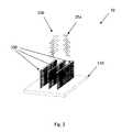
- FIG. 2shows a schematic of the features in one subpixel when light with different polarization impinges thereon.
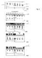
- FIG. 3shows a method of fabricating the device of FIG. 1 .
- FIG. 4is a perspective view of the device according one embodiment.
- FIG. 5shows a method of fabricating the device of FIG. 4 .
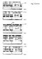
- FIG. 6is a perspective view of the device according one embodiment.
- FIG. 7shows a method of fabricating the device of FIG. 6 .
- FIG. 8is a perspective view of the device according one embodiment.
- FIG. 9shows a method of fabricating the device of FIG. 8 .
- FIG. 10shows a polarization detector array with the device of FIG. 1 , 4 , 6 or 8 integrated therein.
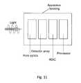
- FIG. 11shows a schematic of a light detector apparatus wherein the device of FIG. 1 , 4 , 6 or 8 is used as fore optics.
- FIG. 12shows a top view and a perspective view of a feature in the device of FIG. 1 , wherein the feature has metal layers on its sidewalls.
- featuremeans a structure whose dimensions in a direction perpendicular to the substrate (hereafter referred to as the “normal direction”) and in the transverse direction are substantially greater than a dimension of the structure in a direction perpendicular to both the normal direction and the transverse direction (hereafter referred to as the “thickness direction”).
- a featurecan have any suitable shape in a cross-section parallel to the substrate, such as a rectangle, an ellipse, convex-convex (i.e. like a double-convex lens), concave-concave (i.e. like a double-concave lens), plano-convex (i.e.
- plano-concavei.e. like a plano-concave lens
- the plurality of featurescan be equally or unequally spaced from each other.
- the plurality of features in different subpixelsare functional to react differently to light with a same polarization.
- the term “react”is meant to broadly encompass absorbing, reflecting, coupling to, detecting, interacting with, converting to electrical signals, etc.
- the plurality of features in a first subpixelextends in a first transverse direction; the plurality of features in a second subpixel extends in a second transverse direction, wherein the first and second pixels are adjacent and the first transverse direction is different from the second transverse direction.
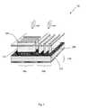
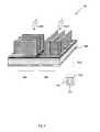
- FIG. 1shows a device 10 according to one embodiment.
- the device 10can comprise a plurality of pixels such as more than 100, more than 1000, more than 1000000.
- the subpixelspreferably have a pitch of about 1 micron to 100 microns (more preferably 5 microns).
- the device 10comprises a plurality of features 100 (e.g. at least 2 features), respectively.
- the features 100 in the subpixel 10 a and the features 100 in the subpixel 10 bextend in different transverse directions.
- the features 100preferably have a pitch (i.e.
- each of the features 100forms a p-i-n diode with the substrate 110 , the p-i-n diode being functional to convert at least a portion of light impinged thereon to an electrical signal.
- Each feature 100comprises a heavily doped semiconductor layer 124 disposed on a lightly doped semiconductor layer or intrinsic semiconductor layer 121 .
- the substrate 110comprises another lightly doped semiconductor layer 122 of an opposite type from the heavily doped semiconductor layer 124 .
- the lightly doped semiconductor layer or intrinsic semiconductor layer 121 of the feature 100is disposed on the lightly doped semiconductor layer 122 .
- the layers 121 , 122 and 124form the p-i-n diode. Space between the features 100 can be filled with a transparent material.
- the device 10preferably further comprises electrical components configured to detect the electrical signal from the features 100 , for example, a transparent electrode disposed on each subpixel and electrically connected to all features 100 therein.
- the transparent electrode on each subpixelpreferably is separate from the transparent electrode on adjacent subpixels.
- a reflective materialcan be deposited on areas of the substrate 110 between the features 100 .
- the substrate 110can have a thickness in the normal direction of about 5 to 700 microns (preferably 120 microns).
- FIG. 2shows a schematic of the features 100 in one subpixel when light with different polarization impinges thereon.
- the absorptance of the features 100is about 35%.
- the absorptance of the features 100is about 95%.
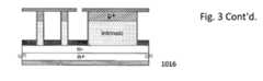
- FIG. 3shows an exemplary method of fabrication of the device 10 .
- a silicon substrate 110is provided, wherein the silicon substrate comprises an intrinsic layer or a lightly doped n type silicon epitaxial layer 121 , a heavily doped n type layer 123 and a lightly doped n type layer 122 sandwiched between the layers 121 and 123 .
- a substrate of semiconductor material other than silicone.g. III-V or II-VI group compound semiconductor can also be used.
- a heavily doped p type layer 124is fabricated on the layer 121 by a method such as ion implantation and subsequent annealing.
- An exemplary dopant suitable for use in the ion implantationis boron or boron difluoride.
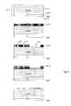
- a resist layer 125(e.g. a photoresist or an e-beam resist) is deposited on the heavily doped p type layer 124 , by a suitable method such as spin coating.
- a patternis formed in the resist layer 125 using a lithography technique (e.g. photolithrograph or e-beam lithography) by removing portions 126 of the resist layer 125 .
- the heavily doped p type layer 124is exposed under the removed portions 126 .
- the patterncorresponds to shapes and positions of the features 100 .
- a metal layer 125is deposited on the resist layer 125 and the exposed portions of the heavily doped p type layer 124 , using a suitable technique such as thermal evaporation, e-beam evaporation, and sputtering.
- exemplary metal suitable for use in the metal layer 125are aluminum, gold, chromium, silver, copper, titanium, nickel or a combination thereof.
- step 1005remainder of the resist layer 125 and portions of the metal layer 125 thereon are lift-off by a suitable technique such as plasma ashing and dissolution in a suitable solvent.
- step 1006features 100 are formed by etching into the substrate 110 using a suitable technique, such as dry etching with remainder of the metal layer 125 as etch mask, until portions of the lightly doped n type layer 122 not directly below the remainder of the metal layer 125 are exposed.
- the features 100now comprise remainder of the layers 121 and 124 .
- a layer of oxide 128(e.g. HfO 2 , SiO 2 , Al 2 O 3 ) is deposited isotropically over the features 100 and exposed portions of the layer 122 , using suitable technique such as atomic layer deposition (ALD) and chemical vapor deposition (CVD).
- ALDatomic layer deposition
- CVDchemical vapor deposition
- the layer of oxide 128is functional to passivate surfaces of the features 100 .
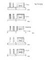
- a metal layer 130is deposited on the heavily doped n type layer 123 using a suitable technique such as thermal evaporation, e-beam evaporation, and sputtering.
- exemplary metal suitable for use in the metal layer 130are aluminum, gold, chromium, silver, copper, titanium, nickel or a combination thereof.
- a rapid thermal annealingcan be conducted following the deposition of the metal layer 130 to form an Ohmic contact between the metal 130 and the heavily doped n type layer 123 .
- a reflective layer 129is deposited anisotropically on and between the features 100 such that sidewalls of the features 100 are preferably free of the reflective layer 129 .
- the reflective layer 129can be deposited by thermal evaporation or e-beam evaporation.
- Exemplary metal suitable for use in the reflective layer 129are aluminum, gold, chromium, silver, copper, titanium, nickel or a combination thereof.
- a sacrificial layer 131preferably with a refractive index lower than that of the features 100 is deposited by spin coating or evaporation to fill space between the features 100 .
- the sacrificial layer 131can be a suitable material such as polyimide or oxide.
- step 1011the sacrificial layer 131 is planarized using a suitable technique such as chemical mechanical polishing (CMP) until the heavily doped p type layer 124 of the features 100 is exposed.
- CMPchemical mechanical polishing
- a transparent conductive oxide (TCO) layer 132is deposited on the sacrificial layer 131 and the exposed heavily doped p type layer 124 of the features 100 , using a suitable method such as thermal evaporation, e-beam evaporation, and sputtering.
- the TCO layercan comprise one or more suitable materials such as indium tin oxide, aluminum zinc oxide, zinc indium oxide, zinc oxide and graphene.
- step 1013another resist layer 133 is deposited on the TCO layer 132 using a technique such as spin-coating.
- a patternis formed in the resist layer 133 using a lithography technique (e.g. photolithrograph or e-beam lithography) by removing portions 134 of the resist layer 133 .
- the TCO layer 132is exposed under the removed portions 134 .
- the patterncorresponds to gaps to be made in the TCO layer 132 for electrically separating the TCO layer 132 into transparent electrodes for each subpixel.
- step 1014the TCO layer 132 is dry etched using the resist layer 133 as etch mask until portions of the sacrificial layer 131 is exposed in the removed portions 134 of the resist layer 133 .
- step 1015remainder of the resist layer 133 is removed by plasma ashing or dissolution in a suitable solvent.
- the sacrificial layer 131is optionally removed by a suitable method such as wet etching.
- a suitable methodsuch as wet etching.
- polyimidecan be removed by a suitable photoresist developer.
- a thermal annealinge.g. at 450° C. for 30 minutes
- FIG. 4shows a device 20 according to one embodiment.
- the device 20can comprise a plurality of pixels such as more than 100, more than 1000, more than 1000000.
- the subpixelspreferably have a pitch of about 1 micron to 100 microns (more preferably 5 microns).
- the device 20comprises a plurality of features 200 (e.g. at least 2 features), respectively.
- the features 200 in the subpixel 20 a and the features 200 in the subpixel 20 bextend in different transverse directions.
- the features 200preferably have a pitch (i.e.
- each of the features 200forms a p-i-n diode with the substrate 210 , the p-i-n diode being functional to convert at least a portion of light impinged thereon to an electrical signal.
- Each feature 200comprises a core 221 of lightly doped semiconductor or intrinsic semiconductor, and a shell 223 of heavily doped semiconductor, the shell 223 being conformally disposed over the core 221 .
- the substrate 210comprises a lightly doped semiconductor layer 222 of an opposite type from the shell 223 .
- the core 221is disposed on the lightly doped semiconductor layer 222 .
- the shell 223 , core 221 and layer 222form the p-i-n diode. Space between the features 200 can be filled with a transparent material.
- the device 20preferably further comprises electrical components configured to detect the electrical signal from the features 200 , for example, an electrode disposed between and electrically connected to the features 200 on each subpixel.
- the electrode disposed between the features 200 on each subpixelpreferably is separate from the electrode disposed between the features 200 on adjacent subpixels.
- the electrodecan also function as a reflective layer.
- the substrate 210can have a thickness in the normal direction of about 5 to 700 microns (preferably 120 microns).
- FIG. 5shows an exemplary method of fabrication of the device 20 .
- a silicon substrate 210is provided, wherein the silicon substrate comprises an intrinsic layer or a lightly doped n type silicon epitaxial layer 221 , a heavily doped n type layer 223 and a lightly doped n type layer 222 sandwiched between the layers 221 and 223 .
- a substrate of semiconductor material other than silicone.g. III-V or II-VI group compound semiconductor can also be used.
- a resist layer 225(e.g. a photoresist or an e-beam resist) is deposited on the layer 221 , by a suitable method such as spin coating.
- a patternis formed in the resist layer 225 using a lithography technique (e.g. photolithrograph or e-beam lithography) by removing portions 226 of the resist layer 225 .
- the layer 221is exposed under the removed portions 226 .
- the patterncorresponds to shapes and positions of the features 200 .
- a metal layer 227is deposited on the resist layer 225 and the exposed portions of the layer 221 , using a suitable technique such as thermal evaporation, e-beam evaporation, and sputtering.
- exemplary metal suitable for use in the metal layer 227are aluminum, gold, chromium, silver, copper, titanium, nickel or a combination thereof.
- step 2004remainder of the resist layer 225 and portions of the metal layer 227 thereon are lift-off by a suitable technique such as plasma ashing and dissolution in a suitable solvent.
- features 200are formed by etching into the substrate 210 using a suitable technique, such as dry etching with remainder of the metal layer 227 as etch mask, until portions of the lightly doped n type layer 222 not directly below the remainder of the metal layer 227 are exposed.
- the features 200now comprise remainder of the layer 221 .
- step 2006remainder of the metal layer 227 is removed by a suitable technique such as wet etching with a suitable metal etchant.
- a resist layer 229(e.g. a photoresist or an e-beam resist) is deposited on the layer 222 and the features 200 , by a suitable method such as spin coating.
- the resist layer 229is then patterned using a lithography technique to expose portions of the layer 222 at boundaries of the subpixels.
- a silicon nitride or aluminum oxide layer 230is deposited anisotropically over the exposed portions of the layer 222 and on the resist layer 229 using a suitable technique such as thermal evaporation, e-beam evaporation, and sputtering.
- step 2009remainder of the resist layer 229 and any portions of the layer 230 thereon are removed by plasma ashing or dissolution in a suitable solvent.
- a p-type dopant layer 231is deposited isotropically over the features 200 , remainder of on the layer 230 , and the layer 222 , using a suitable technique such as ALD or CVD.
- ALDis preferred.
- the p-type dopant layer 231can comprise a suitable p-type dopant such as trimethyboron, triiospropylborane, triethoxyborane, triisopropoxyborane, and a combination thereof.
- an oxide layer 232is deposited isotropically over the p-type dopant layer 231 using a suitable technique such as ALD or CVD.
- a heavily doped p type layer 233is formed by annealing the device 20 to diffuse the p-type dopant layer 231 into the layer 222 .
- the annealingcan be done in a suitable atmosphere (e.g. argon) at about 850° C. for 10 to 30 minutes.
- step 2013the oxide layer 232 is removed by a suitable method such as etching with buffered HF followed by washing. Now the heavily doped p type layer 233 is exposed.
- a layer of oxide 234(e.g. HfO 2 , SiO 2 , Al 2 O 3 ) is deposited isotropically over the layer 233 and remainder of on the layer 230 , using suitable technique such as atomic layer deposition (ALD) and chemical vapor deposition (CVD).
- ALDatomic layer deposition
- CVDchemical vapor deposition
- the layer of oxide 234is functional to passivate surfaces of the layer 233 .
- a resist layer 235(e.g. a photoresist or an e-beam resist) is deposited on the layer 234 , by a suitable method such as spin coating.
- the resist layer 235is then patterned using a lithography technique to expose portions of the layer 234 .
- exposed portions of the layer 234is removed by a suitable technique such as dry etching to expose portions of the layer 233 .
- the resist layer 235is then removed by ashing or dissolution in a suitable solvent.
- a resist layer 237(e.g. a photoresist or an e-beam resist) is deposited on the layers 233 and 234 , by a suitable method such as spin coating.
- the resist layer 237is then patterned using a lithography technique such that only the features 200 and the layer 230 remain under the resist layer 237 .
- a metal layer 239is deposited anisotropically on and between the features 200 such that sidewalls of the features 200 are preferably free of the metal layer 239 .
- the metal layer 239can be deposited by thermal evaporation or e-beam evaporation.
- Exemplary metal suitable for use in the metal layer 239are aluminum, gold, chromium, silver, copper, titanium, nickel or a combination thereof.
- the resist layer 237is then removed by plasma ashing or dissolution in a suitable solvent.
- step 2019the device 20 is annealed under a suitable atmosphere (e.g. H 2 and N 2 ) at about 450° C. for about 30 minutes, such that the metal layer 239 and the exposed portions of the heavily doped p type layer 233 form an Ohmic contact.
- a suitable atmospheree.g. H 2 and N 2
- a resist layer 238(e.g. a photoresist or an e-beam resist) is deposited on the layers 239 and 234 , by a suitable method such as spin coating.
- the resist layer 238is then patterned using a lithography technique to expose the remainder of the layer 230 and any portion of the layer 234 thereon.
- a metal layer 241is deposited anisotropically over the oxide layer 240 , using a suitable technique such as thermal evaporation or e-beam evaporation.
- the metal layer 241is optically opaque.
- step 2023the resist layer 238 and any portions of the oxide layer 240 and the metal layer 241 thereon are removed by a suitable technique such as plasma ashing and dissolution in a suitable solvent.
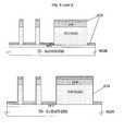
- FIG. 6shows a device 30 according to one embodiment.
- the device 30can comprise a plurality of pixels such as more than 100, more than 1000, more than 1000000.
- the subpixelspreferably have a pitch of about 1 micron to 100 microns (more preferably 5 microns).
- the device 30comprises a plurality of features 300 (e.g. at least 2 features), respectively.
- the features 300 in the subpixel 30 a and the features 300 in the subpixel 30 bextend in different transverse directions.
- the features 300preferably have a pitch (i.e.
- Each of the features 300preferably comprises a p-i-n diode, the p-i-n diode being functional to convert at least a portion of light impinged thereon to an electrical signal.
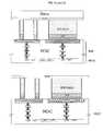
- Each feature 300comprises a core 321 of lightly doped semiconductor, an intermediate shell 331 of intrinsic semiconductor and an outer shell 332 of doped semiconductor.
- the intermediate shell 331is conformally disposed over the core 321 .
- the outer shell 332is conformally disposed over the intermediate shell 331 .
- the outer shell 332is of an opposite type from the core 321 .
- the outer shell 332 , the intermediate shell 331 and the core 321form the p-i-n diode.
- Space between the features 300can be filled with a transparent material.
- the device 20preferably further comprises electrical components configured to detect the electrical signal from the features 300 , for example, an electrode disposed between and electrically connected to the features 300 on each subpixel.
- the electrode disposed between the features 300 on each subpixelpreferably is separate from the electrode disposed between the features 300 on adjacent subpixels.
- the electrodecan also function as a reflective layer.
- the substrate 310can have a thickness in the normal direction of about 5 to 700 microns (preferably 120 microns).
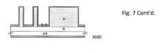
- FIG. 7shows an exemplary method of fabrication of the device 30 .
- a silicon substrate 310is provided, wherein the silicon substrate comprises a lightly doped n type silicon epitaxial layer 321 , a heavily doped n type layer 323 and a n type layer 322 sandwiched between the layers 321 and 323 .
- a substrate of semiconductor material other than silicone.g. III-V or II-VI group compound semiconductor can also be used.
- a resist layer 325(e.g. a photoresist or an e-beam resist) is deposited on the layer 321 , by a suitable method such as spin coating.
- a patternis formed in the resist layer 325 using a lithography technique (e.g. photolithrograph or e-beam lithography) by removing portions 326 of the resist layer 325 .
- the layer 321is exposed under the removed portions 326 .
- the patterncorresponds to shapes and positions of the features 300 .
- a metal layer 327is deposited on the resist layer 325 and the exposed portions of the layer 321 , using a suitable technique such as thermal evaporation, e-beam evaporation, and sputtering.
- exemplary metal suitable for use in the metal layer 327are aluminum, gold, chromium, silver, copper, titanium, nickel or a combination thereof.
- step 3004remainder of the resist layer 325 and portions of the metal layer 327 thereon are lift-off by a suitable technique such as plasma ashing and dissolution in a suitable solvent.
- features 300are formed by etching into the substrate 310 using a suitable technique, such as dry etching with remainder of the metal layer 327 as etch mask, until portions of the lightly doped n type layer 322 not directly below the remainder of the metal layer 327 are exposed.
- the features 300now comprise remainder of the layer 321 .
- step 3006remainder of the metal layer 327 is removed by a suitable technique such as wet etching with a suitable metal etchant.
- a resist layer 329(e.g. a photoresist or an e-beam resist) is deposited on the layer 322 and the features 300 , by a suitable method such as spin coating.
- the resist layer 329is then patterned using a lithography technique to expose portions of the layer 322 at boundaries of the subpixels.
- a silicon nitride or aluminum oxide layer 330is deposited anisotropically over the exposed portions of the layer 322 and on the resist layer 329 using a suitable technique such as thermal evaporation, e-beam evaporation, and sputtering.
- step 3009remainder of the resist layer 329 and any portions of the layer 330 thereon are removed by plasma ashing or dissolution in a suitable solvent.
- an intrinsic amorphous silicon (a-Si) layer 331is deposited isotropically over the features 300 , remainder of on the layer 330 , and the layer 322 , using a suitable technique such as ALD or CVD.
- ALDis preferred.
- a p type doped a-Si layer 332is deposited isotropically over the layer 331 using a suitable technique such as ALD or CVD.
- the device 30is then annealed in a suitable atmosphere (e.g. forming gas) at about 450° C. for about 30 minutes.
- a resist layer 333(e.g. a photoresist or an e-beam resist) is deposited on the layer 332 , by a suitable method such as spin coating.
- the resist layer 333is then patterned using a lithography technique to expose any portion of the layer 332 on the remainder of the layer 330 .
- step 3013exposed portions of the layer 332 and any portion of the layer 331 thereunder are removed by a suitable method such as dry etch, until the layer 330 is exposed.
- step 3014the resist layer 333 is removed by plasma ashing or dissolution in a suitable solvent.
- a resist layer 334(e.g. a photoresist or an e-beam resist) is deposited by a suitable method such as spin coating.
- the resist layer 334is then patterned using a lithography technique such that only the features 300 and the layer 330 remain under the resist layer 334 .
- a metal layer 335is deposited anisotropically on and between the features 300 such that sidewalls of the features 300 are preferably free of the metal layer 335 .
- a metal layer 336is deposited on the layer 323 .
- the metal layers 335 and 336can be deposited by thermal evaporation or e-beam evaporation.
- Exemplary metal suitable for use in the metal layer 335are aluminum, gold, chromium, silver, copper, titanium, nickel or a combination thereof.
- step 3017the resist layer 334 and any portion of the metal layer 335 thereon are removed by plasma ashing or dissolution in a suitable solvent.
- the device 30is then annealed under a suitable atmosphere (e.g. H 2 and N 2 ) at about 450° C. for about 30 minutes, such that the metal layers 335 and 336 form Ohmic contacts with the layer 332 and 323 , respectively.
- a suitable atmospheree.g. H 2 and N 2
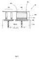
- a resist layer 337(e.g. a photoresist or an e-beam resist) is deposited on the layers 332 and 335 , by a suitable method such as spin coating.
- the resist layer 337is then patterned using a lithography technique to expose the remainder of the layer 330 .
- an oxide layer 338 and a metal layer 339are sequentially deposited anisotropically, using a suitable technique such as thermal evaporation or e-beam evaporation.
- the oxide layer 338is an electrical insulator.
- the metal layer 241is optically opaque.
- step 3020the resist layer 337 and any portions of the oxide layer 338 and the metal layer 339 thereon are removed by a suitable technique such as plasma ashing and dissolution in a suitable solvent.
- FIG. 8shows a device 40 according to one embodiment.
- the device 40can comprise a plurality of pixels such as more than 100, more than 1000, more than 1000000.
- the subpixelspreferably have a pitch of about 1 micron to 100 microns (more preferably 5 microns).
- the device 40comprises a plurality of features 400 (e.g. at least 2 features), respectively.
- the features 400 in the subpixel 40 a and the features 400 in the subpixel 40 bextend in different transverse directions.
- the features 400preferably have a pitch (i.e.
- each of the features 400preferably comprises a p-i-n diode therein, the p-i-n diode being functional to convert at least a portion of light impinged thereon to an electrical signal, wherein the p-i-n diode is formed along the normal direction.
- each feature 400comprises a first heavily doped semiconductor layer 435 , a lightly doped semiconductor layer or intrinsic semiconductor layer 421 , a second heavily doped layer 424 .
- the first heavily doped semiconductor layer 435is disposed on the lightly doped semiconductor layer or intrinsic semiconductor layer 421 .
- the lightly doped semiconductor layer or intrinsic semiconductor layer 421is disposed on the second heavily doped layer 424 .
- the first heavily doped layer 435is of an opposite type from the second heavily doped layer 424 .
- the first heavily doped layer 435 , the lightly doped semiconductor layer or intrinsic semiconductor layer 421 and the second heavily doped layer 424form the p-i-n diode. Space between the features 300 can be filled with a transparent material.
- the features 400preferably are bonded to the substrate 410 .
- the device 40preferably further comprises electrical components configured to detect the electrical signal from the features 400 , for example, Readout Integrated Circuits (ROIC) in the substrate 410 .
- the ROICcan be electrically connected to the second heavily doped layer 424 .
- the substrate 410can have a thickness in the normal direction of about 5 to 700 microns (preferably 120 microns).
- FIG. 9shows an exemplary method of fabrication of the device 40 .
- a silicon substrate 423is provided, wherein the silicon substrate 423 comprises an silicon oxide layer 422 thereon and an intrinsic layer or a lightly doped p type silicon layer 421 on the silicon oxide layer 422 .
- a substrate of semiconductor material other than silicone.g. III-V or II-VI group compound semiconductor can also be used.
- a heavily doped n type layer 424is fabricated on the layer 421 by a method such as ion implantation and subsequent annealing.
- An exemplary dopant suitable for use in the ion implantationis phosphorous or arsenic.
- a resist layer 425(e.g. a photoresist or an e-beam resist) is deposited on the heavily doped n type layer 424 , by a suitable method such as spin coating.
- a patternis formed in the resist layer 425 using a lithography technique (e.g. photolithrograph or e-beam lithography) by removing portions 426 of the resist layer 425 .
- the heavily doped n type layer 424is exposed under the removed portions 426 .
- the patterncorresponds to shapes and positions of the features 400 .
- a metal layer 427is deposited on the resist layer 425 and the exposed portions of the heavily doped n type layer 424 , using a suitable technique such as thermal evaporation, e-beam evaporation, and sputtering.
- exemplary metal suitable for use in the metal layer 427are aluminum, gold, chromium, silver, copper, titanium, nickel or a combination thereof.
- step 4005remainder of the resist layer 425 and portions of the metal layer 427 thereon are lift-off by a suitable technique such as plasma ashing and dissolution in a suitable solvent.
- step 4006features 400 are formed by etching into the layer 421 using a suitable technique, such as dry etching with remainder of the metal layer 125 as etch mask, until portions of the silicon oxide layer 422 not directly below the remainder of the metal layer 427 are exposed.
- the features 400now comprise remainder of the layers 421 and 424 .
- step 4007remainder of the metal layer 427 is removed by a suitable method such as etching with a suitable metal etchant.
- a metal layer 429is deposited anisotropically on the heavily doped n type layer 424 and exposed portions of the silicon oxide layer 422 , using a suitable technique such as thermal evaporation, e-beam evaporation, and sputtering.
- exemplary metal suitable for use in the metal layer 429are aluminum, gold, chromium, silver, copper, titanium, nickel or a combination thereof.
- an oxide layer 428(e.g. HfO 2 , SiO 2 , Al 2 O 3 ) is deposited isotropically over the features 400 and the metal layer 429 , using suitable technique such as atomic layer deposition (ALD) and chemical vapor deposition (CVD).
- ALDatomic layer deposition
- CVDchemical vapor deposition
- step 4010portions of the oxide layer 428 above the metal layer 429 are removed by a suitable technique such as anisotropic dry etch. Now the metal layer 429 is exposed.
- a silicide layer 430is formed from the heavily doped n type layer 424 and portions of the metal layer 429 thereon by annealing the device 40 . Remainder of the metal layer 429 is removed by a suitable technique such as etching with a suitable metal etchant.
- a sacrificial layer 431is deposited by pouring, spin coating or evaporation to fill space between the features 400 .
- the sacrificial layer 431can be a suitable material such as polydimethylsiloxane, polyimide or oxide.
- step 4013the substrate using a suitable technique such as etching with potassium hydroxide, until the silicon oxide layer 422 is exposed.
- a glass substrate 432is bonded to the exposed silicon oxide layer 422 , using a suitable technique such as using a UV removable glue.
- the glass substrate 432can provide mechanical support.
- the sacrificial layeris removed by a suitable method such as wet etching.
- a suitable methodsuch as wet etching.
- polyimidecan be removed by a suitable photoresist developer.
- the features 40are bonded to ROIC in the substrate 410 using a tin-silver alloy layer between the substrate 410 and the features 40 and annealing at about 220° C.
- step 4017the glass substrate 432 is released from the silicon oxide layer 422 by illumination with UV light.
- a heavily doped p type layer 435is formed on the layer 421 of the features 400 by a suitable technique such as ion implantation through the silicon oxide layer 422 .
- the heavily doped p type layer 435can be annealed by laser to activate implanted dopant.
- step 4019the silicon oxide layer 422 is removed by a suitable technique such as etching with HF.
- an insulating material 433is deposited by spin coating, evaporation or CVD to fill space between the features 400 .
- the insulating material 433preferably has a lower refractive index than the features 400 .
- the insulating material 433can be any suitable material such as silicon oxide and polyimide.
- the insulating material 433is planarized using a suitable technique such as chemical mechanical polishing (CMP) until the heavily doped p type layer 432 of the features 400 is exposed.
- CMPchemical mechanical polishing
- a transparent conductive oxide (TCO) layer 434is deposited on the insulating material 433 , using a suitable method such as thermal evaporation, e-beam evaporation, and sputtering.
- the TCO layercan comprise one or more suitable materials such as indium tin oxide, aluminum zinc oxide, zinc oxide, zinc indium oxide and graphene.
- the insulating material 433is optionally removed by a suitable method such as wet etching.
- the device 10 , 20 , 30 or 40can be integrated with electronic circuitry into a polarization detector array.
- the electronic circuitrycan include address decoders in both directions of the detector array, a correlated double sampling circuit (CDS), a signal processor, a multiplexor.
- CDScorrelated double sampling circuit
- the electronic circuitryis functional to detect the electrical signal converted by the features 100 , 200 , 300 or 400 from at least a portion of light impinged thereon.
- the electric circuitrycan be further functional to calculate an interpolation of electrical signals from several subpixels, the features on which extend in the same transverse direction.
- Other function of the electronic circuitrycan include a gain adjustment, a calculation of Stoke's parameters.
- the subpixelscan be arranged into a group (i.e. pixel).
- a subpixel A and subpixels B, C and Dcan be arranged adjacent to each other and referred to as a pixel, wherein features on the subpixels B, C and D extend in transverse directions at 45°, 90° and ⁇ 45° relative to a transverse direction in which features on the subpixel A extend.
- the device 10 , 20 , 30 or 40can also be used as fore optics in a light detector apparatus as shown in the schematic in FIG. 11 .
- the features 100 , 200 , 300 and 400can each comprise a metal layer on each sidewall (i.e. surface extending in the transverse direction and the normal direction).
- the metal layerpreferably has a thickness of about 5 nm to about 100 nm, more preferably about 50 nm.
- the metal layersubstantially covers the entire sidewall and the metal layer does not extend to either end of the features in the normal direction.
Landscapes
- Physics & Mathematics (AREA)
- General Physics & Mathematics (AREA)
- Spectroscopy & Molecular Physics (AREA)
- Light Receiving Elements (AREA)
- Chemical & Material Sciences (AREA)
- Engineering & Computer Science (AREA)
- Materials Engineering (AREA)
- Nanotechnology (AREA)
Abstract
Description
is the Jones vector. Polarization of light with any polarization, including unpolarized, partially polarized, and fully polarized light, can be described by the Stokes parameters, which are four mutually independent parameters.
Claims (36)
Priority Applications (17)
| Application Number | Priority Date | Filing Date | Title |
|---|---|---|---|
| US12/945,492US9515218B2 (en) | 2008-09-04 | 2010-11-12 | Vertical pillar structured photovoltaic devices with mirrors and optical claddings |
| US13/047,392US8835831B2 (en) | 2010-06-22 | 2011-03-14 | Polarized light detecting device and fabrication methods of the same |
| US13/106,851US9082673B2 (en) | 2009-10-05 | 2011-05-12 | Passivated upstanding nanostructures and methods of making the same |
| US13/925,429US9304035B2 (en) | 2008-09-04 | 2013-06-24 | Vertical waveguides with various functionality on integrated circuits |
| US14/450,812US20140339666A1 (en) | 2010-06-22 | 2014-08-04 | Polarized light detecting device and fabrication methods of the same |
| US14/503,598US9410843B2 (en) | 2008-09-04 | 2014-10-01 | Nanowire arrays comprising fluorescent nanowires and substrate |
| US14/516,162US20160111562A1 (en) | 2008-09-04 | 2014-10-16 | Multispectral and polarization-selective detector |
| US14/516,402US20160111460A1 (en) | 2008-09-04 | 2014-10-16 | Back-lit photodetector |
| US14/632,739US9601529B2 (en) | 2008-09-04 | 2015-02-26 | Light absorption and filtering properties of vertically oriented semiconductor nano wires |
| US14/704,143US20150303333A1 (en) | 2008-09-04 | 2015-05-05 | Passivated upstanding nanostructures and methods of making the same |
| US14/705,380US9337220B2 (en) | 2008-09-04 | 2015-05-06 | Solar blind ultra violet (UV) detector and fabrication methods of the same |
| US15/057,153US20160178840A1 (en) | 2008-09-04 | 2016-03-01 | Optical waveguides in image sensors |
| US15/082,514US20160211394A1 (en) | 2008-11-13 | 2016-03-28 | Nano wire array based solar energy harvesting device |
| US15/090,155US20160216523A1 (en) | 2008-09-04 | 2016-04-04 | Vertical waveguides with various functionality on integrated circuits |
| US15/093,928US20160225811A1 (en) | 2008-09-04 | 2016-04-08 | Nanowire structured color filter arrays and fabrication method of the same |
| US15/149,252US20160254301A1 (en) | 2008-09-04 | 2016-05-09 | Solar blind ultra violet (uv) detector and fabrication methods of the same |
| US15/225,264US20160344964A1 (en) | 2008-09-04 | 2016-08-01 | Methods for fabricating and using nanowires |
Applications Claiming Priority (3)
| Application Number | Priority Date | Filing Date | Title |
|---|---|---|---|
| US35742910P | 2010-06-22 | 2010-06-22 | |
| US36042110P | 2010-06-30 | 2010-06-30 | |
| US13/047,392US8835831B2 (en) | 2010-06-22 | 2011-03-14 | Polarized light detecting device and fabrication methods of the same |
Related Parent Applications (2)
| Application Number | Title | Priority Date | Filing Date |
|---|---|---|---|
| US12/982,269Continuation-In-PartUS9299866B2 (en) | 2008-09-04 | 2010-12-30 | Nanowire array based solar energy harvesting device |
| US13/048,635Continuation-In-PartUS8835905B2 (en) | 2008-09-04 | 2011-03-15 | Solar blind ultra violet (UV) detector and fabrication methods of the same |
Related Child Applications (3)
| Application Number | Title | Priority Date | Filing Date |
|---|---|---|---|
| US12/945,492Continuation-In-PartUS9515218B2 (en) | 2008-09-04 | 2010-11-12 | Vertical pillar structured photovoltaic devices with mirrors and optical claddings |
| US13/048,635Continuation-In-PartUS8835905B2 (en) | 2008-09-04 | 2011-03-15 | Solar blind ultra violet (UV) detector and fabrication methods of the same |
| US14/450,812ContinuationUS20140339666A1 (en) | 2008-09-04 | 2014-08-04 | Polarized light detecting device and fabrication methods of the same |
Publications (2)
| Publication Number | Publication Date |
|---|---|
| US20110309240A1 US20110309240A1 (en) | 2011-12-22 |
| US8835831B2true US8835831B2 (en) | 2014-09-16 |
Family
ID=45327814
Family Applications (4)
| Application Number | Title | Priority Date | Filing Date |
|---|---|---|---|
| US13/047,392Expired - Fee RelatedUS8835831B2 (en) | 2008-09-04 | 2011-03-14 | Polarized light detecting device and fabrication methods of the same |
| US13/048,635Expired - Fee RelatedUS8835905B2 (en) | 2008-09-04 | 2011-03-15 | Solar blind ultra violet (UV) detector and fabrication methods of the same |
| US14/450,812AbandonedUS20140339666A1 (en) | 2008-09-04 | 2014-08-04 | Polarized light detecting device and fabrication methods of the same |
| US14/487,375Expired - Fee RelatedUS9054008B2 (en) | 2008-09-04 | 2014-09-16 | Solar blind ultra violet (UV) detector and fabrication methods of the same |
Family Applications After (3)
| Application Number | Title | Priority Date | Filing Date |
|---|---|---|---|
| US13/048,635Expired - Fee RelatedUS8835905B2 (en) | 2008-09-04 | 2011-03-15 | Solar blind ultra violet (UV) detector and fabrication methods of the same |
| US14/450,812AbandonedUS20140339666A1 (en) | 2008-09-04 | 2014-08-04 | Polarized light detecting device and fabrication methods of the same |
| US14/487,375Expired - Fee RelatedUS9054008B2 (en) | 2008-09-04 | 2014-09-16 | Solar blind ultra violet (UV) detector and fabrication methods of the same |
Country Status (1)
| Country | Link |
|---|---|
| US (4) | US8835831B2 (en) |
Cited By (21)
| Publication number | Priority date | Publication date | Assignee | Title |
|---|---|---|---|---|
| US20140264711A1 (en)* | 2013-03-15 | 2014-09-18 | Maxim Integrated Products, Inc. | Light sensor with vertical diode junctions |
| US20140339666A1 (en)* | 2010-06-22 | 2014-11-20 | Zena Technologies, Inc. | Polarized light detecting device and fabrication methods of the same |
| US9082673B2 (en) | 2009-10-05 | 2015-07-14 | Zena Technologies, Inc. | Passivated upstanding nanostructures and methods of making the same |
| US9123841B2 (en) | 2009-12-08 | 2015-09-01 | Zena Technologies, Inc. | Nanowire photo-detector grown on a back-side illuminated image sensor |
| US9177985B2 (en) | 2009-06-04 | 2015-11-03 | Zena Technologies, Inc. | Array of nanowires in a single cavity with anti-reflective coating on substrate |
| US9299866B2 (en) | 2010-12-30 | 2016-03-29 | Zena Technologies, Inc. | Nanowire array based solar energy harvesting device |
| US9304035B2 (en) | 2008-09-04 | 2016-04-05 | Zena Technologies, Inc. | Vertical waveguides with various functionality on integrated circuits |
| US9337220B2 (en) | 2008-09-04 | 2016-05-10 | Zena Technologies, Inc. | Solar blind ultra violet (UV) detector and fabrication methods of the same |
| US9343490B2 (en) | 2013-08-09 | 2016-05-17 | Zena Technologies, Inc. | Nanowire structured color filter arrays and fabrication method of the same |
| US9406709B2 (en) | 2010-06-22 | 2016-08-02 | President And Fellows Of Harvard College | Methods for fabricating and using nanowires |
| US9410843B2 (en) | 2008-09-04 | 2016-08-09 | Zena Technologies, Inc. | Nanowire arrays comprising fluorescent nanowires and substrate |
| US9429723B2 (en) | 2008-09-04 | 2016-08-30 | Zena Technologies, Inc. | Optical waveguides in image sensors |
| US9478685B2 (en) | 2014-06-23 | 2016-10-25 | Zena Technologies, Inc. | Vertical pillar structured infrared detector and fabrication method for the same |
| US9490283B2 (en) | 2009-11-19 | 2016-11-08 | Zena Technologies, Inc. | Active pixel sensor with nanowire structured photodetectors |
| US9515218B2 (en) | 2008-09-04 | 2016-12-06 | Zena Technologies, Inc. | Vertical pillar structured photovoltaic devices with mirrors and optical claddings |
| US9543458B2 (en) | 2010-12-14 | 2017-01-10 | Zena Technologies, Inc. | Full color single pixel including doublet or quadruplet Si nanowires for image sensors |
| US11385104B2 (en)* | 2017-12-22 | 2022-07-12 | Arizona Board Of Regents On Behalf Of Arizona State University | On-chip polarization detection and polarimetric imaging |
| US11487051B2 (en) | 2020-01-24 | 2022-11-01 | Arizona Board Of Regents On Behalf Of Arizona State University | Polarization filters having nanograting pattern and plasmonic structure oriented at nonzero angle |
| US11733552B2 (en) | 2020-03-31 | 2023-08-22 | Arizona Board Of Regents On Behalf Of Arizona State University | Ultra-fast optical modulation and ultra-short pulse generation based on tunable graphene-plasmonic hybrid metasurfaces |
| US11843350B2 (en) | 2020-01-21 | 2023-12-12 | Arizona Board Of Regents On Behalf Of Arizona State University | Autonomous solar field and receiver inspections based on polarimetric-enhanced imaging |
| RU2842161C1 (en)* | 2024-12-05 | 2025-06-23 | Акционерное общество "СКАНДА РУС" | Polarization-resolving photodetector and method for simultaneous determination of intensity and angle of linear polarization of radiation with polarization-resolving photodetector |
Families Citing this family (24)
| Publication number | Priority date | Publication date | Assignee | Title |
|---|---|---|---|---|
| US20160111562A1 (en)* | 2008-09-04 | 2016-04-21 | Zena Technologies, Inc. | Multispectral and polarization-selective detector |
| US8461571B2 (en)* | 2011-06-29 | 2013-06-11 | Nokia Corporation | Method and apparatus for converting photon energy to electrical energy |
| ITTO20110649A1 (en)* | 2011-07-19 | 2013-01-20 | St Microelectronics Srl | PHOTORELECTRIC DEVICE WITH PROTECTIVE AND ANTI-REFLECTIVE COVER, AND RELATIVE MANUFACTURING METHOD |
| US9593053B1 (en)* | 2011-11-14 | 2017-03-14 | Hypersolar, Inc. | Photoelectrosynthetically active heterostructures |
| FR2992472B1 (en)* | 2012-06-20 | 2014-08-08 | Commissariat Energie Atomique | SEMICONDUCTOR OPTICAL RECEIVER WITH PIN STRUCTURE |
| DE102014103467B4 (en) | 2013-03-15 | 2025-07-31 | Maxim Integrated Products, Inc. | Light sensor with vertical diode junctions |
| US12243948B2 (en)* | 2013-05-22 | 2025-03-04 | W&W Sens Devices, Inc. | Microstructure enhanced absorption photosensitive devices |
| US11621360B2 (en)* | 2013-05-22 | 2023-04-04 | W&W Sens Devices, Inc. | Microstructure enhanced absorption photosensitive devices |
| US12087871B2 (en) | 2013-05-22 | 2024-09-10 | W&W Sens Devices, Inc. | Microstructure enhanced absorption photosensitive devices |
| US11791432B2 (en) | 2013-05-22 | 2023-10-17 | W&Wsens Devices, Inc. | Microstructure enhanced absorption photosensitive devices |
| CN105466437A (en)* | 2014-09-12 | 2016-04-06 | 江苏南大五维电子科技有限公司 | Path detection system based on solar blind ultraviolet light signal |
| KR102526997B1 (en)* | 2015-07-31 | 2023-05-02 | 서울바이오시스 주식회사 | Light detecting device and electric appartus using the same |
| KR102399941B1 (en)* | 2015-06-01 | 2022-05-23 | 서울바이오시스 주식회사 | Apparatus for measuring uv and portable terminal comprising the same |
| DE212016000103U1 (en) | 2015-06-01 | 2018-01-14 | Seoul Viosys Co., Ltd. | Ultraviolet measuring device, photodetector element, ultraviolet detector, ultraviolet index calculating device and electronic device with these |
| CN105043944B (en)* | 2015-06-30 | 2017-09-22 | 西安理工大学 | The device and its detection method of haze detection of particles are carried out based on solar blind UV |
| US9625379B2 (en)* | 2015-07-15 | 2017-04-18 | International Business Machines Corporation | Gas sensor with integrated optics and reference cell |
| CN106057957B (en)* | 2016-08-01 | 2017-07-28 | 中国科学技术大学 | Avalanche photodide with periodic nano-structure |
| US11867891B2 (en)* | 2016-12-22 | 2024-01-09 | Advanced Optical Technologies, Inc. | Polarimeter with multiple independent tunable channels and method for material orientation imaging |
| CN110914715B (en)* | 2017-07-26 | 2023-09-22 | 深圳帧观德芯科技有限公司 | Radiation detector and method of making the same |
| EP4053880A1 (en)* | 2018-04-22 | 2022-09-07 | Epinovatech AB | Reinforced thin-film device |
| US12094903B2 (en) | 2019-09-24 | 2024-09-17 | W&W Sens Devices, Inc | Microstructure enhanced absorption photosensitive devices |
| EP3907877A1 (en) | 2020-05-07 | 2021-11-10 | Epinovatech AB | Induction machine |
| CN112885922B (en)* | 2021-01-18 | 2022-09-27 | 西安工业大学 | Photodetector based on PtSe2 and silicon nanopillar array and preparation method thereof |
| CN113658971A (en)* | 2021-07-12 | 2021-11-16 | 浙江大学 | Radiation detector based on graphene charge-coupled device |
Citations (360)
| Publication number | Priority date | Publication date | Assignee | Title |
|---|---|---|---|---|
| US1918848A (en) | 1929-04-26 | 1933-07-18 | Norwich Res Inc | Polarizing refracting bodies |
| US3903427A (en) | 1973-12-28 | 1975-09-02 | Hughes Aircraft Co | Solar cell connections |
| US4017332A (en) | 1975-02-27 | 1977-04-12 | Varian Associates | Solar cells employing stacked opposite conductivity layers |
| US4357415A (en) | 1980-03-06 | 1982-11-02 | Eastman Kodak Company | Method of making a solid-state color imaging device having a color filter array using a photocrosslinkable barrier |
| US4387265A (en) | 1981-07-17 | 1983-06-07 | University Of Delaware | Tandem junction amorphous semiconductor photovoltaic cell |
| US4400221A (en) | 1981-07-08 | 1983-08-23 | The United States Of America As Represented By The Secretary Of The Air Force | Fabrication of gallium arsenide-germanium heteroface junction device |
| US4443890A (en) | 1980-12-02 | 1984-04-17 | Thomson-Csf | Optical-connection direct-light modulation information transmission system with a passband extended towards the low frequencies and continuous waves |
| US4513168A (en) | 1984-04-19 | 1985-04-23 | Varian Associates, Inc. | Three-terminal solar cell circuit |
| WO1986003347A1 (en) | 1984-11-20 | 1986-06-05 | Hughes Aircraft Company | Solid state laser employing diamond having color centers as a laser active material |
| US4620237A (en) | 1984-10-22 | 1986-10-28 | Xerox Corporation | Fast scan jitter measuring system for raster scanners |
| US4827335A (en) | 1986-08-29 | 1989-05-02 | Kabushiki Kaisha Toshiba | Color image reading apparatus with two color separation filters each having two filter elements |
| US4846556A (en) | 1987-05-14 | 1989-07-11 | Toppan Printing Co., Ltd. | Color filter and method of manufacturing the same |
| US4880613A (en) | 1987-01-12 | 1989-11-14 | Sumitomo Electric Industries, Ltd. | Light emitting element comprising diamond and method for producing the same |
| US4896941A (en) | 1985-04-27 | 1990-01-30 | Doryokuro Kakunenryo Kaihatsu Jigyodan | Image-transmitting fiber |
| US4950625A (en) | 1988-06-13 | 1990-08-21 | Sumitomo Electric Industries, Ltd. | Diamond laser crystal and method manufacturing the same |
| US4971928A (en) | 1990-01-16 | 1990-11-20 | General Motors Corporation | Method of making a light emitting semiconductor having a rear reflecting surface |
| US4972244A (en) | 1988-06-16 | 1990-11-20 | Commissariat A L'energie Atomique | Photodiode and photodiode array on a II-VI material and processes for the production thereof |
| US5096520A (en) | 1990-08-01 | 1992-03-17 | Faris Sades M | Method for producing high efficiency polarizing filters |
| US5124543A (en) | 1989-08-09 | 1992-06-23 | Ricoh Company, Ltd. | Light emitting element, image sensor and light receiving element with linearly varying waveguide index |
| US5247349A (en) | 1982-11-16 | 1993-09-21 | Stauffer Chemical Company | Passivation and insulation of III-V devices with pnictides, particularly amorphous pnictides having a layer-like structure |
| US5272518A (en) | 1990-12-17 | 1993-12-21 | Hewlett-Packard Company | Colorimeter and calibration system |
| US5311047A (en) | 1988-11-16 | 1994-05-10 | National Science Council | Amorphous SI/SIC heterojunction color-sensitive phototransistor |
| US5347147A (en) | 1990-11-28 | 1994-09-13 | Jones Barbara L | Light emitting diamond device |
| US5362972A (en) | 1990-04-20 | 1994-11-08 | Hitachi, Ltd. | Semiconductor device using whiskers |
| US5374841A (en) | 1991-12-18 | 1994-12-20 | Texas Instruments Incorporated | HgCdTe S-I-S two color infrared detector |
| US5401968A (en) | 1989-12-29 | 1995-03-28 | Honeywell Inc. | Binary optical microlens detector array |
| US5449626A (en) | 1991-12-27 | 1995-09-12 | Hezel; Rudolf | Method for manufacture of a solar cell |
| US5468652A (en) | 1993-07-14 | 1995-11-21 | Sandia Corporation | Method of making a back contacted solar cell |
| US5602661A (en) | 1993-02-17 | 1997-02-11 | Hoffmann-La Roche Inc. | Optical component |
| US5612780A (en) | 1996-06-05 | 1997-03-18 | Harris Corporation | Device for detecting light emission from optical fiber |
| US5671914A (en) | 1995-11-06 | 1997-09-30 | Spire Corporation | Multi-band spectroscopic photodetector array |
| US5696863A (en) | 1982-08-06 | 1997-12-09 | Kleinerman; Marcos Y. | Distributed fiber optic temperature sensors and systems |
| US5723945A (en) | 1996-04-09 | 1998-03-03 | Electro Plasma, Inc. | Flat-panel display |
| US5747796A (en) | 1995-07-13 | 1998-05-05 | Sharp Kabushiki Kaisha | Waveguide type compact optical scanner and manufacturing method thereof |
| US5767507A (en) | 1996-07-15 | 1998-06-16 | Trustees Of Boston University | Polarization sensitive photodetectors and detector arrays |
| US5798535A (en) | 1996-12-20 | 1998-08-25 | Motorola, Inc. | Monolithic integration of complementary transistors and an LED array |
| US5844290A (en) | 1996-06-27 | 1998-12-01 | Nec Corporation | Solid state image pick-up device and method for manufacturing the same |
| US5853446A (en) | 1996-04-16 | 1998-12-29 | Corning Incorporated | Method for forming glass rib structures |
| US5857053A (en) | 1997-06-17 | 1999-01-05 | Lucent Technologies Inc. | Optical fiber filter |
| US5877492A (en) | 1995-09-14 | 1999-03-02 | Nec Corporation | Contact type image sensor comprising a plurality of microlenses |
| US5880495A (en) | 1998-01-08 | 1999-03-09 | Omnivision Technologies, Inc. | Active pixel with a pinned photodiode |
| US5900623A (en) | 1997-08-11 | 1999-05-04 | Chrontel, Inc. | Active pixel sensor using CMOS technology with reverse biased photodiodes |
| US5943463A (en) | 1996-06-17 | 1999-08-24 | Sharp Kabushiki Kaisha | Color image sensor and a production method of an optical waveguide array for use therein |
| WO2000002379A1 (en) | 1998-07-01 | 2000-01-13 | Cmos Sensor, Inc. | Silicon butting contact image sensor chip with line transfer and pixel readout (ltpr) structure |
| US6033582A (en) | 1996-01-22 | 2000-03-07 | Etex Corporation | Surface modification of medical implants |
| US6037243A (en) | 1997-11-06 | 2000-03-14 | Electronics And Telecommunications Research Institute | Method for manufacturing silicon nanometer structure using silicon nitride film |
| US6046466A (en) | 1997-09-12 | 2000-04-04 | Nikon Corporation | Solid-state imaging device |
| US6074892A (en) | 1996-05-07 | 2000-06-13 | Ciena Corporation | Semiconductor hetero-interface photodetector |
| US6100551A (en) | 1995-04-13 | 2000-08-08 | Eastman Kodak Company | Active pixel sensor integrated with a pinned photodiode |
| GB2348399A (en) | 1999-03-31 | 2000-10-04 | Univ Glasgow | Reactive ion etching with control of etch gas flow rate, pressure and rf power |
| US6270548B1 (en) | 1997-04-17 | 2001-08-07 | James Wilbert Campbell | Sintering process for diamond and diamond growth |
| US6301420B1 (en) | 1998-05-01 | 2001-10-09 | The Secretary Of State For Defence In Her Britannic Majesty's Government Of The United Kingdom Of Great Britain And Northern Ireland | Multicore optical fibre |
| US6326649B1 (en) | 1999-01-13 | 2001-12-04 | Agere Systems, Inc. | Pin photodiode having a wide bandwidth |
| US20020003201A1 (en) | 1998-02-02 | 2002-01-10 | Gang Yu | Image sensors made from organic semiconductors |
| US20020021879A1 (en) | 2000-07-10 | 2002-02-21 | Lee Kevin K. | Graded index waveguide |
| US20020020846A1 (en) | 2000-04-20 | 2002-02-21 | Bo Pi | Backside illuminated photodiode array |
| US6388648B1 (en) | 1996-11-05 | 2002-05-14 | Clarity Visual Systems, Inc. | Color gamut and luminance matching techniques for image display systems |
| US6388243B1 (en) | 1999-03-01 | 2002-05-14 | Photobit Corporation | Active pixel sensor with fully-depleted buried photoreceptor |
| JP2002151715A (en) | 2000-11-08 | 2002-05-24 | Sharp Corp | Thin film solar cell |
| US6407439B1 (en) | 1999-08-19 | 2002-06-18 | Epitaxial Technologies, Llc | Programmable multi-wavelength detector array |
| US20020104821A1 (en) | 1996-10-04 | 2002-08-08 | Michael Bazylenko | Reactive ion etching of silica structures |
| US20020109082A1 (en) | 2001-02-13 | 2002-08-15 | Yoshikazu Nakayama And Daiken Chemical Co., Ltd. | Light receiving and emitting probe and light receiving and emitting probe apparatus |
| US20020130311A1 (en) | 2000-08-22 | 2002-09-19 | Lieber Charles M. | Doped elongated semiconductors, growing such semiconductors, devices including such semiconductors and fabricating such devices |
| US6459034B2 (en) | 2000-06-01 | 2002-10-01 | Sharp Kabushiki Kaisha | Multi-junction solar cell |
| US6463204B1 (en) | 1998-12-18 | 2002-10-08 | Fujitsu Network Communications, Inc. | Modular lightpipe system |
| US20020172820A1 (en) | 2001-03-30 | 2002-11-21 | The Regents Of The University Of California | Methods of fabricating nanostructures and nanowires and devices fabricated therefrom |
| US20030003300A1 (en) | 2001-07-02 | 2003-01-02 | Korgel Brian A. | Light-emitting nanoparticles and method of making same |
| US20030006363A1 (en) | 2001-04-27 | 2003-01-09 | Campbell Scott Patrick | Optimization of alignment between elements in an image sensor |
| US6542231B1 (en) | 2000-08-22 | 2003-04-01 | Thermo Finnegan Llc | Fiber-coupled liquid sample analyzer with liquid flow cell |
| US20030077907A1 (en) | 1999-08-06 | 2003-04-24 | Kao David Y. | Method for forming an etch mask during the manufacture of a semiconductor device |
| US6563995B2 (en) | 2001-04-02 | 2003-05-13 | Lightwave Electronics | Optical wavelength filtering apparatus with depressed-index claddings |
| US20030089899A1 (en) | 2000-08-22 | 2003-05-15 | Lieber Charles M. | Nanoscale wires and related devices |
| US6566723B1 (en) | 2002-01-10 | 2003-05-20 | Agilent Technologies, Inc. | Digital color image sensor with elevated two-color photo-detector and related circuitry |
| US20030103744A1 (en) | 2001-02-28 | 2003-06-05 | Yoshimi Koyama | Image input device |
| US20030132480A1 (en) | 2002-01-16 | 2003-07-17 | Duc Chau | Self-aligned trench mosfets and methods for making the same |
| US20030189202A1 (en) | 2002-04-05 | 2003-10-09 | Jun Li | Nanowire devices and methods of fabrication |
| US20030227090A1 (en) | 2002-05-31 | 2003-12-11 | Ichiro Okabe | Dual damascene semiconductor devices |
| WO2003107439A1 (en) | 2002-06-12 | 2003-12-24 | Rwe Schott Solar, Inc. | Photovoltaic module with light reflecting backskin |
| US6680216B2 (en) | 2000-03-09 | 2004-01-20 | General Electric Company | Method of making imager structure |
| US20040026684A1 (en) | 2002-04-02 | 2004-02-12 | Nanosys, Inc. | Nanowire heterostructures for encoding information |
| US6709929B2 (en) | 2001-06-25 | 2004-03-23 | North Carolina State University | Methods of forming nano-scale electronic and optoelectronic devices using non-photolithographically defined nano-channel templates |
| US20040058058A1 (en) | 2000-04-12 | 2004-03-25 | Shchegolikhin Alexander Nikitovich | Raman-active taggants and thier recognition |
| US20040065362A1 (en) | 2001-01-31 | 2004-04-08 | Takenori Watabe | Solar cell and method for producing the same |
| US6720594B2 (en) | 2002-01-07 | 2004-04-13 | Xerox Corporation | Image sensor array with reduced pixel crosstalk |
| US20040075464A1 (en) | 2002-07-08 | 2004-04-22 | Btg International Limited | Nanostructures and methods for manufacturing the same |
| US20040109666A1 (en) | 2002-12-10 | 2004-06-10 | John Kim | Optoelectronic devices employing fibers for light collection and emission |
| US20040122328A1 (en) | 2000-06-19 | 2004-06-24 | University Of Washington | Integrated optical scanning image acquisition and display |
| US20040118377A1 (en) | 2002-12-19 | 2004-06-24 | Bloms Jason K. | Fuel allocation at idle or light engine load |
| US20040118337A1 (en) | 2002-09-30 | 2004-06-24 | Canon Kabushiki Kaisha | Method for growing silicon film, method for manufacturing solar cell, semiconductor substrate, and solar cell |
| US20040124366A1 (en) | 2002-10-02 | 2004-07-01 | Haishan Zeng | Apparatus and methods relating to high speed spectroscopy and excitation-emission matrices |
| US6771314B1 (en) | 1998-03-31 | 2004-08-03 | Intel Corporation | Orange-green-blue (OGB) color system for digital image sensor applications |
| US20040155247A1 (en) | 2000-12-21 | 2004-08-12 | Stephan Benthien | Image sensor device comprising central locking |
| US20040180461A1 (en) | 2003-03-12 | 2004-09-16 | Taiwan Semiconductor Manufacturing Company | Light guide for image sensor |
| US6805139B1 (en) | 1999-10-20 | 2004-10-19 | Mattson Technology, Inc. | Systems and methods for photoresist strip and residue treatment in integrated circuit manufacturing |
| US20040213307A1 (en) | 2002-07-19 | 2004-10-28 | President And Fellows Of Harvard College | Nanoscale coherent optical components |
| US6812473B1 (en) | 1999-06-30 | 2004-11-02 | Hoya Corporation | Electron beam drawing mask blank, electron beam drawing mask, and method of manufacturing the same |
| US20040217086A1 (en) | 2002-09-11 | 2004-11-04 | Matsushita Electric Industrial Co., Ltd. | Pattern formation method |
| US20040223681A1 (en) | 2003-04-23 | 2004-11-11 | Block Bruce A. | On-chip optical signal routing |
| US20040241965A1 (en) | 2003-05-28 | 2004-12-02 | Charles Merritt | High aspect ratio microelectrode arrays |
| US20040261840A1 (en) | 2003-06-30 | 2004-12-30 | Advent Solar, Inc. | Emitter wrap-through back contact solar cells on thin silicon wafers |
| US20050009224A1 (en) | 2003-06-20 | 2005-01-13 | The Regents Of The University Of California | Nanowire array and nanowire solar cells and methods for forming the same |
| US20050082676A1 (en) | 2003-10-17 | 2005-04-21 | International Business Machines Corporation | Silicon chip carrier with through-vias using laser assisted chemical vapor deposition of conductor |
| US20050087601A1 (en) | 2003-10-24 | 2005-04-28 | Gerst Carl W.Iii | Light pipe illumination system and method |
| US20050095699A1 (en) | 2002-10-30 | 2005-05-05 | Akihiro Miyauchi | Functioning substrate with a group of columnar micro pillars and its manufacturing method |
| US20050116271A1 (en) | 2003-12-02 | 2005-06-02 | Yoshiaki Kato | Solid-state imaging device and manufacturing method thereof |
| US20050133476A1 (en) | 2003-12-17 | 2005-06-23 | Islam M. S. | Methods of bridging lateral nanowires and device using same |
| WO2005064337A1 (en) | 2003-12-22 | 2005-07-14 | Koninklijke Philips Electronics N.V. | Optical nanowire biosensor based on energy transfer |
| US20050164514A1 (en) | 2004-01-28 | 2005-07-28 | Shahid Rauf | Method for etching a quartz layer in a photoresistless semiconductor mask |
| US6927145B1 (en) | 2004-02-02 | 2005-08-09 | Advanced Micro Devices, Inc. | Bitline hard mask spacer flow for memory cell scaling |
| US20050190453A1 (en) | 2004-03-01 | 2005-09-01 | Hideki Dobashi | Image sensor |
| US20050201704A1 (en) | 2004-02-12 | 2005-09-15 | Panorama Flat Ltd. | Apparatus, method, and computer program product for transverse waveguided display system |
| JP2005252210A (en) | 2004-02-03 | 2005-09-15 | Sharp Corp | Solar cell |
| US20050218468A1 (en) | 2004-03-18 | 2005-10-06 | Owen Mark D | Micro-reflectors on a substrate for high-density LED array |
| US6960526B1 (en) | 2003-10-10 | 2005-11-01 | The United States Of America As Represented By The Secretary Of The Army | Method of fabricating sub-100 nanometer field emitter tips comprising group III-nitride semiconductors |
| US20050242409A1 (en) | 2004-04-28 | 2005-11-03 | Advanced Chip Engineering Technology Inc. | Imagine sensor with a protection layer |
| US6967120B2 (en) | 2002-07-19 | 2005-11-22 | Dongbu Anam Semiconductor | Pinned photodiode for a CMOS image sensor and fabricating method thereof |
| US6969899B2 (en) | 2003-12-08 | 2005-11-29 | Taiwan Semiconductor Manufacturing Co., Ltd. | Image sensor with light guides |
| US20050284517A1 (en) | 2004-06-29 | 2005-12-29 | Sanyo Electric Co., Ltd. | Photovoltaic cell, photovoltaic cell module, method of fabricating photovoltaic cell and method of repairing photovoltaic cell |
| US6987258B2 (en) | 2001-12-19 | 2006-01-17 | Intel Corporation | Integrated circuit-based compound eye image sensor using a light pipe bundle |
| US20060011362A1 (en) | 2002-01-14 | 2006-01-19 | China Petroleum & Chemical Corporation | Power transmission unit of an impactor, a hydraulic jet impactor and the application thereof |
| US7052927B1 (en) | 2004-01-27 | 2006-05-30 | Raytheon Company | Pin detector apparatus and method of fabrication |
| US20060113622A1 (en) | 2004-11-30 | 2006-06-01 | International Business Machines Corporation | A damascene copper wiring image sensor |
| US20060121371A1 (en) | 2004-12-03 | 2006-06-08 | Innolux Display Corp. | Color filter having nanoparticles for liquid crystal display |
| US7064372B2 (en) | 2002-09-30 | 2006-06-20 | Nanosys, Inc. | Large-area nanoenabled macroelectronic substrates and uses therefor |
| US20060146323A1 (en) | 2005-01-06 | 2006-07-06 | Alexandre Bratkovski | Nanowires for surface-enhanced raman scattering molecular sensors |
| US20060162766A1 (en) | 2003-06-26 | 2006-07-27 | Advent Solar, Inc. | Back-contacted solar cells with integral conductive vias and method of making |
| EP0809303B1 (en) | 1996-05-22 | 2006-09-06 | Eastman Kodak Company | A color active pixel sensor with electronic shuttering, anti-blooming and low cross-talk |
| US7105428B2 (en) | 2004-04-30 | 2006-09-12 | Nanosys, Inc. | Systems and methods for nanowire growth and harvesting |
| US7109517B2 (en) | 2001-11-16 | 2006-09-19 | Zaidi Saleem H | Method of making an enhanced optical absorption and radiation tolerance in thin-film solar cells and photodetectors |
| US7135698B2 (en)* | 2002-12-05 | 2006-11-14 | Lockheed Martin Corporation | Multi-spectral infrared super-pixel photodetector and imager |
| US20060260674A1 (en) | 2004-04-06 | 2006-11-23 | Tran Bao Q | Nano ic |
| US20060273389A1 (en) | 2005-05-23 | 2006-12-07 | International Business Machines Corporation | Vertical FET with nanowire channels and a silicided bottom contact |
| US20060273262A1 (en) | 2000-12-20 | 2006-12-07 | Michel Sayag | Light stimulating and collecting methods and apparatus for storage-phosphor image plates |
| US20060284118A1 (en) | 2005-06-15 | 2006-12-21 | Board Of Trustees Of Michigan State University | Process and apparatus for modifying a surface in a work region |
| US7153720B2 (en) | 2002-12-09 | 2006-12-26 | Quantum Semiconductor Llc | CMOS image sensor |
| US7163659B2 (en) | 2002-12-03 | 2007-01-16 | Hewlett-Packard Development Company, L.P. | Free-standing nanowire sensor and method for detecting an analyte in a fluid |
| US20070012985A1 (en) | 2004-03-23 | 2007-01-18 | Nanosys, Inc. | Nanowire capacitor and methods of making same |
| US20070023799A1 (en) | 2005-08-01 | 2007-02-01 | Micro Technology, Inc. | Structure and method for building a light tunnel for use with imaging devices |
| US20070025504A1 (en) | 2003-06-20 | 2007-02-01 | Tumer Tumay O | System for molecular imaging |
| US20070029545A1 (en) | 2003-02-24 | 2007-02-08 | Ignis Innovation Inc | Pixel having an organic light emitting diode and method of fabricating the pixel |
| US20070052050A1 (en) | 2005-09-07 | 2007-03-08 | Bart Dierickx | Backside thinned image sensor with integrated lens stack |
| US20070076481A1 (en) | 2005-10-03 | 2007-04-05 | Rockwell Scientific Licensing, Llc | Multimode focal plane array with electrically isolated commons for independent sub-array biasing |
| US20070082255A1 (en) | 2005-10-06 | 2007-04-12 | Gongquan Sun | Fuel cells and fuel cell catalysts incorporating a nanoring support |
| US7208783B2 (en) | 2004-11-09 | 2007-04-24 | Micron Technology, Inc. | Optical enhancement of integrated circuit photodetectors |
| US20070099292A1 (en) | 2001-04-10 | 2007-05-03 | Bioprocessors Corp. | Reactor systems having a light-interacting component |
| US20070104441A1 (en) | 2005-11-08 | 2007-05-10 | Massachusetts Institute Of Technology | Laterally-integrated waveguide photodetector apparatus and related coupling methods |
| US20070108371A1 (en) | 2005-11-16 | 2007-05-17 | Eastman Kodak Company | PMOS pixel structure with low cross talk for active pixel image sensors |
| US20070120254A1 (en) | 2003-12-23 | 2007-05-31 | Koninklijke Philips Electronics N.C. | Semiconductor device comprising a pn-heterojunction |
| US20070126037A1 (en) | 2005-12-06 | 2007-06-07 | Sotomitsu Ikeda | Electric device having nanowires, manufacturing method thereof, and electric device assembly |
| US20070138459A1 (en) | 2005-10-13 | 2007-06-21 | Wong Stanislaus S | Ternary oxide nanostructures and methods of making same |
| US20070138376A1 (en) | 2005-08-24 | 2007-06-21 | The Trustees Of Boston College | Nanoscale optical microscope |
| US20070140638A1 (en) | 2004-05-13 | 2007-06-21 | The Regents Of The University Of California | Nanowires and nanoribbons as subwavelength optical waveguides and their use as components in photonic circuits and devices |
| US20070139740A1 (en) | 2005-12-20 | 2007-06-21 | Fujitsu Limited | Image processing circuit and image processing method |
| US20070137697A1 (en) | 2005-08-24 | 2007-06-21 | The Trustees Of Boston College | Apparatus and methods for solar energy conversion using nanoscale cometal structures |
| US20070138380A1 (en) | 2005-12-16 | 2007-06-21 | Adkisson James W | Funneled light pipe for pixel sensors |
| US7235475B2 (en) | 2004-12-23 | 2007-06-26 | Hewlett-Packard Development Company, L.P. | Semiconductor nanowire fluid sensor and method for fabricating the same |
| US20070148599A1 (en) | 2005-09-13 | 2007-06-28 | Randall True | Multiple step printing methods for microbarcodes |
| US20070145512A1 (en) | 2004-09-27 | 2007-06-28 | Rhodes Howard E | Photogate stack with nitride insulating cap over conductive layer |
| US20070155025A1 (en) | 2006-01-04 | 2007-07-05 | Anping Zhang | Nanowire structures and devices for use in large-area electronics and methods of making the same |
| US20070152248A1 (en) | 2006-01-05 | 2007-07-05 | Korea Advanced Institute Of Science & Technology | Complementary metal oxide semiconductor image sensor and method for fabricating the same |
| US7241434B2 (en) | 2000-08-11 | 2007-07-10 | Bellataire International, Llc | High pressure and high temperature production of diamonds |
| US20070172623A1 (en) | 2003-12-18 | 2007-07-26 | Tesa Ag | Optical data store with several storage layers |
| US20070170418A1 (en) | 2005-12-02 | 2007-07-26 | Bowers Michael J | Broad-emission nanocrystals and methods of making and using same |
| JP2007201091A (en) | 2006-01-25 | 2007-08-09 | Fujifilm Corp | Manufacturing method of solid-state imaging device |
| US20070187787A1 (en) | 2006-02-16 | 2007-08-16 | Ackerson Kristin M | Pixel sensor structure including light pipe and method for fabrication thereof |
| US7262400B2 (en) | 2005-12-02 | 2007-08-28 | Taiwan Semiconductor Manufacturing Co., Ltd. | Image sensor device having an active layer overlying a substrate and an isolating region in the active layer |
| US20070200054A1 (en) | 2006-02-24 | 2007-08-30 | Tower Semiconductor Ltd. | Via wave guide with curved light concentrator for image sensing devices |
| US7265328B2 (en) | 2005-08-22 | 2007-09-04 | Micron Technology, Inc. | Method and apparatus providing an optical guide for an imager pixel having a ring of air-filled spaced slots around a photosensor |
| US20070205483A1 (en) | 2006-01-27 | 2007-09-06 | Williams R S | Mixed-scale electronic interface |
| US7272287B2 (en) | 2005-05-11 | 2007-09-18 | Fitel Usa Corp | Optical fiber filter for suppression of amplified spontaneous emission |
| US20070217754A1 (en) | 2005-10-07 | 2007-09-20 | Takashi Sasaki | Optical fiber, optical transmission line, optical module and optical transmission system |
| US20070228421A1 (en) | 2005-12-06 | 2007-10-04 | Shunsuke Shioya | Semiconductor device using semiconductor nanowire and display apparatus and image pick-up apparatus using the same |
| US20070238265A1 (en) | 2005-04-05 | 2007-10-11 | Keiichi Kurashina | Plating apparatus and plating method |
| US20070238285A1 (en) | 2006-03-31 | 2007-10-11 | Applied Materials, Inc. | Method for making an improved thin film solar cell interconnect using etch and deposition process |
| US20070241260A1 (en) | 2004-09-30 | 2007-10-18 | Osram Opto Semiconductors Gmbh | Radiation detector with an epitaxially grown semiconductor body |
| US7285812B2 (en) | 2004-09-02 | 2007-10-23 | Micron Technology, Inc. | Vertical transistors |
| US20070248958A1 (en) | 2004-09-15 | 2007-10-25 | Microchip Biotechnologies, Inc. | Microfluidic devices |
| US20070246689A1 (en) | 2006-04-11 | 2007-10-25 | Jiaxin Ge | Transparent thin polythiophene films having improved conduction through use of nanomaterials |
| US20070272828A1 (en) | 2006-05-24 | 2007-11-29 | Micron Technology, Inc. | Method and apparatus providing dark current reduction in an active pixel sensor |
| US7307327B2 (en) | 2005-08-04 | 2007-12-11 | Micron Technology, Inc. | Reduced crosstalk CMOS image sensors |
| US7306963B2 (en) | 2004-11-30 | 2007-12-11 | Spire Corporation | Precision synthesis of quantum dot nanostructures for fluorescent and optoelectronic devices |
| US20070285378A1 (en) | 2006-06-09 | 2007-12-13 | Philips Lumileds Lighting Company, Llc | LED Backlight for LCD with Color Uniformity Recalibration Over Lifetime |
| US20070290193A1 (en) | 2006-01-18 | 2007-12-20 | The Board Of Trustees Of The University Of Illinois | Field effect transistor devices and methods |
| US7311889B2 (en) | 2002-06-19 | 2007-12-25 | Fujitsu Limited | Carbon nanotubes, process for their production, and catalyst for production of carbon nanotubes |
| US20080001498A1 (en) | 2005-07-18 | 2008-01-03 | Fritz Muller | Driving apparatus for a linear motion of elongated bodies |
| US20080029701A1 (en) | 2006-07-25 | 2008-02-07 | Matsushita Electric Industrial Co. Ltd. | Night-vision imaging apparatus, control method of the same, and headlight module |
| US7330404B2 (en) | 2003-10-10 | 2008-02-12 | Seagate Technology Llc | Near-field optical transducers for thermal assisted magnetic and optical data storage |
| US20080036038A1 (en) | 2006-03-10 | 2008-02-14 | Hersee Stephen D | PULSED GROWTH OF CATALYST-FREE GROWITH OF GaN NANOWIRES AND APPLICATION IN GROUP III NITRIDE SEMICONDUCTOR BULK MATERIAL |
| US20080044984A1 (en) | 2006-08-16 | 2008-02-21 | Taiwan Semiconductor Manufacturing Co., Ltd. | Methods of avoiding wafer breakage during manufacture of backside illuminated image sensors |
| US7336860B2 (en) | 2003-04-07 | 2008-02-26 | Eksigent Technologies, Llc | Microfluidic detection device having reduced dispersion and method for making same |
| US7335962B2 (en) | 2004-07-08 | 2008-02-26 | Micron Technology, Inc. | Photonic crystal-based lens elements for use in an image sensor |
| US20080047604A1 (en) | 2006-08-25 | 2008-02-28 | General Electric Company | Nanowires in thin-film silicon solar cells |
| US20080047601A1 (en) | 2006-08-22 | 2008-02-28 | Somnath Nag | High Efficiency Solar Cells and Manufacturing Methods |
| US20080055451A1 (en) | 2006-08-29 | 2008-03-06 | Sony Corporation | Solid-state imaging device and imaging apparatus |
| US20080065451A1 (en) | 2006-09-08 | 2008-03-13 | Hon Hai Precision Industry Co., Ltd. | System and method for converting electronic orders to work orders |
| US20080073742A1 (en) | 2006-09-26 | 2008-03-27 | Adkisson James W | Stacked image package |
| US20080079076A1 (en) | 2006-09-29 | 2008-04-03 | Dong Sun Sheen | Semiconductor device having reduced standby leakage current and increased driving current and method for manufacturing the same |
| US20080079022A1 (en) | 2006-09-29 | 2008-04-03 | Kazushige Yamamoto | Optical device having photoelectric conversion layer |
| US20080083963A1 (en) | 2006-10-04 | 2008-04-10 | International Business Machines Corporation | P-i-n semiconductor diodes and methods of forming the same |
| US20080090401A1 (en) | 2006-10-17 | 2008-04-17 | Alexandre Bratkovski | Independently addressable interdigitated nanowires |
| US20080096308A1 (en) | 2006-10-13 | 2008-04-24 | Charles Santori | Methods for coupling diamond structures to photonic devices |
| US20080108170A1 (en) | 2004-12-23 | 2008-05-08 | International Business Machines Corporation | Cmos imager with cu wiring and method of eliminating high reflectivity interfaces therefrom |
| US20080116537A1 (en) | 2006-11-17 | 2008-05-22 | Adkisson James W | Cmos imager array with recessed dielectric |
| US7381966B2 (en) | 2006-04-13 | 2008-06-03 | Integrated Micro Sensors, Inc. | Single-chip monolithic dual-band visible- or solar-blind photodetector |
| US20080128760A1 (en) | 2006-12-04 | 2008-06-05 | Electronics And Telecommunications Research Institute | Schottky barrier nanowire field effect transistor and method for fabricating the same |
| WO2008069565A1 (en) | 2006-12-05 | 2008-06-12 | Lg Chem, Ltd. | Method for high resolution ink-jet print using pre-patterned substrate and conductive substrate manufactured using the same |
| US20080149944A1 (en) | 2006-12-22 | 2008-06-26 | Qunano Ab | Led with upstanding nanowire structure and method of producing such |
| WO2008079076A1 (en) | 2006-12-22 | 2008-07-03 | Qunano Ab | Led with upstanding nanowire structure and method of producing such |
| US20080157253A1 (en) | 2006-04-13 | 2008-07-03 | Integrated Micro Sensors Inc. | Single-Chip Monolithic Dual-Band Visible- or Solar-Blind Photodetector |
| US20080166883A1 (en) | 2006-01-04 | 2008-07-10 | Taiwan Semiconductor Manufacturing Co., Ltd. | Hemi-spherical structure and method for fabricating the same |
| US20080169019A1 (en) | 2007-01-11 | 2008-07-17 | General Electric Company | Nanowall Solar Cells and Optoelectronic Devices |
| US20080169017A1 (en) | 2007-01-11 | 2008-07-17 | General Electric Company | Multilayered Film-Nanowire Composite, Bifacial, and Tandem Solar Cells |
| US20080173615A1 (en) | 2006-12-04 | 2008-07-24 | Jin Wuk Kim | Etch resist solution, method of fabricating thin film pattern using the same and method of fabricating an LCD device using the same |
| US20080188029A1 (en) | 2003-07-02 | 2008-08-07 | Rhodes Howard E | Pinned photodiode structure and method of formation |
| US20080191298A1 (en) | 2007-02-09 | 2008-08-14 | Intersil Americas Inc. | Ambient light detectors using conventional cmos image sensor process |
| US20080191278A1 (en) | 2004-03-26 | 2008-08-14 | Semiconductor Energy Laboratory Co., Ltd. | Semiconductor device, method for manufacturing the same, liquid crystal television, and EL television |
| US20080211945A1 (en) | 2007-01-10 | 2008-09-04 | Jong-Wook Hong | Image sensor with extended dynamic range |
| US20080218740A1 (en) | 2006-04-28 | 2008-09-11 | Williams R Stanley | Nanowire-based photonic devices |
| US20080224115A1 (en) | 2003-12-22 | 2008-09-18 | Erik Petrus Antonius Maria Bakkers | Fabricating a Set of Semiconducting Nanowires, and Electric Device Comprising a Set of Nanowires |
| US20080225140A1 (en) | 2007-03-16 | 2008-09-18 | Stmicroelectronics (Research & Development) Limited | Image sensors |
| US20080233280A1 (en) | 2007-03-22 | 2008-09-25 | Graciela Beatriz Blanchet | Method to form a pattern of functional material on a substrate by treating a surface of a stamp |
| US20080237568A1 (en) | 2007-04-02 | 2008-10-02 | Nobuhiko Kobayashi | Methods of making nano-scale structures having controlled size, nanowire structures and methods of making the nanowire structures |
| US20080246123A1 (en) | 2007-04-09 | 2008-10-09 | Kamins Theodore I | Methods for controlling catalyst nanoparticle positioning and apparatus for growing a nanowire |
| US20080248304A1 (en) | 2003-07-08 | 2008-10-09 | Brian Korgel | Growth of single crystal nanowires |
| US20080246020A1 (en) | 2006-06-20 | 2008-10-09 | Takahiro Kawashima | Nanowire, method for fabricating the same, and device having nanowires |
| US20080251780A1 (en) | 2007-04-11 | 2008-10-16 | General Electric Company | Light-emitting device and article |
| US20080258747A1 (en) | 2007-04-19 | 2008-10-23 | Oc Oerlikon Balzers Ag | Test equipment for automated quality control of thin film solar modules |
| US20080260225A1 (en) | 2004-10-06 | 2008-10-23 | Harold Szu | Infrared Multi-Spectral Camera and Process of Using Infrared Multi-Spectral Camera |
| US20080266556A1 (en) | 2007-04-25 | 2008-10-30 | Kamins Theodore I | Nanowire configured to couple electromagnetic radiation to selected guided wave, devices using same, and methods of fabricating same |
| WO2008131313A2 (en) | 2007-04-18 | 2008-10-30 | Invisage Technologies, Inc. | Materials systems and methods for optoelectronic devices |
| TW200845402A (en) | 2006-10-26 | 2008-11-16 | Omnivision Tech Inc | Image sensor having curved micro-mirrors over the sensing photodiode and method for fabricating |
| US20080283883A1 (en) | 2007-05-16 | 2008-11-20 | Cheon Man Shim | Image Sensor and Method for Manufacturing the Same |
| US20080283728A1 (en) | 2007-05-15 | 2008-11-20 | Sony Corporation | Solid-state image pickup device and a method of manufacturing the same, and image pickup apparatus |
| WO2008143727A2 (en) | 2007-02-27 | 2008-11-27 | The Regents Of The University Of California | Nanowire photodetector and image sensor with internal gain |
| US20080297281A1 (en) | 2007-06-01 | 2008-12-04 | Georgia Tech Research Corporation | Piezo-on-diamond resonators and resonator systems |
| US7462774B2 (en) | 2003-05-21 | 2008-12-09 | Nanosolar, Inc. | Photovoltaic devices fabricated from insulating nanostructured template |
| US20080311693A1 (en) | 2005-06-03 | 2008-12-18 | Graeme Douglas Maxwell | Method of Aligning Optical Components With Waveguides |
| US20080311712A1 (en) | 2005-08-18 | 2008-12-18 | Anwar Abul F | Insulated gate silicon nanowire transistor and method of manufacture |
| US7471428B2 (en) | 2004-03-12 | 2008-12-30 | Seiko Epson Corporation | Contact image sensor module and image reading device equipped with the same |
| US20090001498A1 (en) | 2007-06-26 | 2009-01-01 | Shih-Yuan Wang | Nanowire photodiodes and methods of making nanowire photodiodes |
| US20090020150A1 (en) | 2007-07-19 | 2009-01-22 | Atwater Harry A | Structures of ordered arrays of semiconductors |
| US20090032687A1 (en) | 2007-08-01 | 2009-02-05 | Silverbrook Research Pty Ltd | Two dimensional contact image sensor with frontlighting |
| US7491269B2 (en) | 2001-12-04 | 2009-02-17 | Thales | Method for catalytic growth of nanotubes or nanofibers comprising a NiSi alloy diffusion barrier |
| US20090046362A1 (en) | 2007-04-10 | 2009-02-19 | Lingjie Jay Guo | Roll to roll nanoimprint lithography |
| US20090046749A1 (en) | 2004-08-04 | 2009-02-19 | Kiminori Mizuuchi | Coherent light source |
| US20090050204A1 (en) | 2007-08-03 | 2009-02-26 | Illuminex Corporation. | Photovoltaic device using nanostructured material |
| US20090057650A1 (en) | 2000-08-22 | 2009-03-05 | President And Fellows Of Harvard College | Nanoscale wires and related devices |
| WO2008135905A3 (en) | 2007-05-07 | 2009-03-12 | Nxp Bv | A photosensitive device and a method of manufacturing a photosensitive device |
| US7507293B2 (en) | 2002-10-28 | 2009-03-24 | Hewlett-Packard Development Company, L.P. | Photonic crystals with nanowire-based fabrication |
| TW200915551A (en) | 2007-05-10 | 2009-04-01 | Koninkl Philips Electronics Nv | Spectrum detector and manufacturing method therefore |
| US20090127442A1 (en) | 2007-11-20 | 2009-05-21 | Hong-Wei Lee | Anti-resonant reflecting optical waveguide for imager light pipe |
| US20090146198A1 (en) | 2007-12-11 | 2009-06-11 | Samsung Electronics Co., Ltd | Photodiodes, image sensing devices and image sensors |
| US20090151782A1 (en) | 2007-12-18 | 2009-06-18 | Lg Electronics Inc. | Hetero-junction silicon solar cell and fabrication method thereof |
| US20090153961A1 (en)* | 2005-07-22 | 2009-06-18 | Zeon Corporation | Grid Polarizer and Method for Manufacturing the Same |
| US20090165844A1 (en) | 2007-12-31 | 2009-07-02 | Banpil Photonics Inc. | Hybrid photovoltaic device |
| US20090173976A1 (en) | 2002-09-19 | 2009-07-09 | Augusto Carlos J R P | Light-Sensing Device for Multi-Spectral Imaging |
| US20090179289A1 (en) | 2004-11-29 | 2009-07-16 | Samsung Electronics Co., Ltd. | Image sensor microlens structures and methods of forming the same |
| US20090189145A1 (en) | 2008-01-30 | 2009-07-30 | Shih-Yuan Wang | Photodetectors, Photovoltaic Devices And Methods Of Making The Same |
| US20090189144A1 (en) | 2008-01-29 | 2009-07-30 | Nathaniel Quitoriano | Device For Absorbing Or Emitting Light And Methods Of Making The Same |
| US20090188552A1 (en) | 2008-01-30 | 2009-07-30 | Shih-Yuan Wang | Nanowire-Based Photovoltaic Cells And Methods For Fabricating The Same |
| US20090199597A1 (en) | 2008-02-07 | 2009-08-13 | Danley Jeffrey D | Systems and methods for collapsing air lines in nanostructured optical fibers |
| US20090201400A1 (en) | 2008-02-08 | 2009-08-13 | Omnivision Technologies, Inc. | Backside illuminated image sensor with global shutter and storage capacitor |
| US20090206405A1 (en) | 2008-02-15 | 2009-08-20 | Doyle Brian S | Fin field effect transistor structures having two dielectric thicknesses |
| US7582587B2 (en) | 2003-02-11 | 2009-09-01 | Eurecat S.A. | Passivation of sulphur hydroconversion catalyst |
| US7582857B2 (en)* | 2006-04-18 | 2009-09-01 | The Trustees Of The University Of Pennsylvania | Sensor and polarimetric filters for real-time extraction of polarimetric information at the focal plane |
| US20090224349A1 (en) | 2006-11-15 | 2009-09-10 | International Business Machines Corporation | Image sensor including spatially different active and dark pixel interconnect patterns |
| US20090224245A1 (en) | 2006-09-29 | 2009-09-10 | Semiconductor Energy Laboratory Co., Ltd. | Display device |
| US20090233445A1 (en) | 2008-03-12 | 2009-09-17 | City University Of Hong Kong | Method of making diamond nanopillars |
| WO2009116018A2 (en) | 2008-03-21 | 2009-09-24 | Oerlikon Trading Ag, Trübbach | Photovoltaic cell and methods for producing a photovoltaic cell |
| US20090244514A1 (en) | 2008-03-26 | 2009-10-01 | Samsung Electronics Co., Ltd. | Distance measuring sensors including vertical photogate and three-dimensional color image sensors including distance measuring sensors |
| US20090243016A1 (en) | 2008-03-27 | 2009-10-01 | Texas Instruments Incorporated | Semiconductor device |
| US7598482B1 (en) | 2005-07-29 | 2009-10-06 | Imec | Wavelength-sensitive detector with elongate nanostructures |
| US20090260687A1 (en) | 2008-04-03 | 2009-10-22 | Samsung Electronics Co., Ltd. | Solar cell |
| US20090261438A1 (en) | 2008-04-17 | 2009-10-22 | Choi Kyoung Jin | Visible-range semiconductor nanowire-based photosensor and method for manufacturing the same |
| US20090272423A1 (en) | 2003-06-26 | 2009-11-05 | Kyocera Corporation | Multi-Junction Type Solar Cell Device |
| US20090278998A1 (en) | 2007-09-27 | 2009-11-12 | Ostendo Technologies, Inc. | Quantum Photonic Imagers and Methods of Fabrication Thereof |
| US7622367B1 (en) | 2004-06-04 | 2009-11-24 | The Board Of Trustees Of The University Of Illinois | Methods and devices for fabricating and assembling printable semiconductor elements |
| US20090289320A1 (en) | 2008-05-21 | 2009-11-26 | International Business Machines Corporation | Fast p-i-n photodetector with high responsitivity |
| US7646943B1 (en) | 2008-09-04 | 2010-01-12 | Zena Technologies, Inc. | Optical waveguides in image sensors |
| US7646138B2 (en) | 2006-11-21 | 2010-01-12 | Interuniversitair Microelektronica Centrum (Imec) | Diamond enhanced thickness shear mode resonator |
| US20100006817A1 (en) | 2008-07-09 | 2010-01-14 | Qunano Ab | Optoelectronic semiconductor device |
| US7647695B2 (en) | 2003-12-30 | 2010-01-19 | Lockheed Martin Corporation | Method of matching harnesses of conductors with apertures in connectors |
| US20100019296A1 (en) | 2008-07-24 | 2010-01-28 | Cha Dae-Kil | Image sensor having nanodot |
| US20100019355A1 (en) | 2008-07-25 | 2010-01-28 | Theodore I Kamins | Multi-Level Nanowire Structure And Method Of Making The Same |
| US20100019252A1 (en) | 2008-07-24 | 2010-01-28 | Alexandre Bratkovski | Nanowire-Based Light-Emitting Diodes and Light-Detection Devices With Nanocrystalline Outer Surface |
| US7655860B2 (en) | 2005-04-01 | 2010-02-02 | North Carolina State University | Nano-structured photovoltaic solar cell and related methods |
| WO2010019887A1 (en) | 2008-08-14 | 2010-02-18 | Brookhaven Science Associates | Structured pillar electrodes |
| US7692860B2 (en)* | 2006-12-07 | 2010-04-06 | Cheil Industries, Inc. | Wire grid polarizer and method of manufacturing the same |
| WO2009137241A9 (en) | 2008-04-14 | 2010-04-08 | Bandgap Engineering, Inc. | Process for fabricating nanowire arrays |
| WO2010039631A1 (en) | 2008-09-30 | 2010-04-08 | The Regents Of The University Of California | Photonic crystal solar cell |
| US20100090341A1 (en) | 2008-10-14 | 2010-04-15 | Molecular Imprints, Inc. | Nano-patterned active layers formed by nano-imprint lithography |
| US7704806B2 (en) | 2005-04-07 | 2010-04-27 | Lg Display Co., Ltd. | Thin film transistor having silicon nanowire and method of fabricating the same |
| US20100104494A1 (en) | 2008-10-24 | 2010-04-29 | Meng Yu-Fei | Enhanced Optical Properties of Chemical Vapor Deposited Single Crystal Diamond by Low-Pressure/High-Temperature Annealing |
| US20100101633A1 (en) | 2008-10-23 | 2010-04-29 | Min Park | Photovoltaic device and method for manufacturing the same |
| US20100110433A1 (en)* | 2008-10-24 | 2010-05-06 | Thales | Polarimetric imaging device optimized for polarization contrast |
| US7713779B2 (en) | 2004-07-21 | 2010-05-11 | Commissariat A L'energie Atomique | Photoactive nanocomposite and method for the production thereof |
| US20100116976A1 (en) | 2008-11-13 | 2010-05-13 | Zena Technologies, Inc. | Vertical waveguides with various functionality on integrated circuits |
| US7719688B2 (en) | 2007-04-24 | 2010-05-18 | Hewlett-Packard Development Company, L.P. | Optical device and method of making the same |
| US20100132779A1 (en) | 2007-05-30 | 2010-06-03 | Jusung Engineering Co., Ltd. | Solar cell and method of fabricating the same |
| US20100136721A1 (en) | 2005-08-14 | 2010-06-03 | Samsung Electronics Co., Ltd. | Nitride-based white light emitting device and manufacturing method thereof |
| US20100133986A1 (en) | 2008-12-03 | 2010-06-03 | Yoon-Jin Kim | Light emission device and display device using same as light source |
| US7732839B2 (en) | 2005-10-26 | 2010-06-08 | Panasonic Corporation | Semiconductor device and method for fabricating the same |
| US7732769B2 (en) | 2005-11-08 | 2010-06-08 | General Atomics | Apparatus and methods for use in flash detection |
| US7736954B2 (en) | 2005-08-26 | 2010-06-15 | Sematech, Inc. | Methods for nanoscale feature imprint molding |
| US20100148221A1 (en) | 2008-11-13 | 2010-06-17 | Zena Technologies, Inc. | Vertical photogate (vpg) pixel structure with nanowires |
| US7740824B2 (en) | 2002-11-21 | 2010-06-22 | Herman Philip Godfried | Optical quality diamond material |
| US20100163714A1 (en) | 2008-09-04 | 2010-07-01 | Zena Technologies, Inc. | Optical waveguides in image sensors |
| US20100163941A1 (en) | 2008-12-30 | 2010-07-01 | Seung-Man Jung | Image sensor and method for manufacturing the same |
| US20100200065A1 (en) | 2009-02-12 | 2010-08-12 | Kyu Hyun Choi | Photovoltaic Cell and Fabrication Method Thereof |
| US20100207103A1 (en) | 2007-06-20 | 2010-08-19 | New Jersey Institute Of Technology | Method of Forming Nanotube Vertical Field Effect Transistor |
| US20100218816A1 (en) | 2009-11-19 | 2010-09-02 | International Business Machines Corporation | Grid-line-free contact for a photovoltaic cell |
| US20100230653A1 (en) | 2009-03-16 | 2010-09-16 | Industrial Technology Research Institute | Phase-change memory element and method for fabricating the same |
| US20100229939A1 (en) | 2009-03-13 | 2010-09-16 | Shen Kuo-Hung | Thin-film solar cell |
| US20100237454A1 (en) | 2006-09-07 | 2010-09-23 | Sony Corporation | Light-receiving device and method for manufacturing light-receiving device |
| US20100244108A1 (en) | 2009-03-31 | 2010-09-30 | Glenn Eric Kohnke | Cmos image sensor on a semiconductor-on-insulator substrate and process for making same |
| US20100249877A1 (en) | 2007-11-21 | 2010-09-30 | The Trustees Of Boston College | Apparatus and Methods for Visual Perception Using an Array of Nanoscale Waveguides |
| US20100244169A1 (en) | 2009-03-31 | 2010-09-30 | Sony Corporation | Solid-state imaging device, fabrication method thereof, imaging apparatus, and fabrication method of anti-reflection structure |
| US20100258184A1 (en) | 2009-04-09 | 2010-10-14 | E. I. Du Pont De Nemours And Company | Glass compositions used in conductors for photovoltaic cells |
| US20100277607A1 (en) | 2007-09-28 | 2010-11-04 | Regents Of The University Of Minnesota | Image sensor with high dynamic range imaging and integrated motion detection |
| US20100276572A1 (en) | 2005-06-02 | 2010-11-04 | Sony Corporation | Semiconductor image sensor module and method of manufacturing the same |
| US20100282314A1 (en) | 2009-05-06 | 2010-11-11 | Thinsilicion Corporation | Photovoltaic cells and methods to enhance light trapping in semiconductor layer stacks |
| US20100302440A1 (en) | 2009-05-26 | 2010-12-02 | Zena Technologies, Inc. | Determination of optimal diameters for nanowires |
| US20100304061A1 (en) | 2009-05-26 | 2010-12-02 | Zena Technologies, Inc. | Fabrication of high aspect ratio features in a glass layer by etching |
| US20100308214A1 (en) | 2009-06-04 | 2010-12-09 | Zena Technologies, Inc. | Array of nanowires in a single cavity with anti-reflective coating on substrate |
| US20100320444A1 (en) | 2009-06-22 | 2010-12-23 | Banpil Photonics, Inc. | Integrated Image Sensor System on Common Substrate |
| US20110037133A1 (en) | 2009-08-17 | 2011-02-17 | Tzung-I Su | Semiconductor Photodetector Structure and the Fabrication Method Thereof |
| US20110036396A1 (en) | 2008-04-30 | 2011-02-17 | The Regents Of The University Of California | Method and apparatus for fabricating optoelectromechanical devices by structural transfer using re-usable substrate |
| US20110080508A1 (en) | 2006-03-24 | 2011-04-07 | Panasonic Corporation | Solid-state image pickup device |
| US20110127490A1 (en) | 2009-11-30 | 2011-06-02 | The Royal Institution For The Advancement Of Learning / Mcgill University | Method of Growing Uniform Semiconductor Nanowires without Foreign Metal Catalyst and Devices Thereof |
| US20110133060A1 (en) | 2009-12-08 | 2011-06-09 | Zena Technologies, Inc. | Active pixel sensor with nanowire structured photodetectors |
| US20110133160A1 (en) | 2009-12-08 | 2011-06-09 | Zena Technologies, Inc. | Nanowire structured photodiode with a surrounding epitaxially grown p or n layer |
| US20110139176A1 (en) | 2009-12-11 | 2011-06-16 | David Cheung | Low damage photoresist strip method for low-k dielectrics |
| US20110147870A1 (en) | 2008-02-15 | 2011-06-23 | Kah Wee Ang | Photodetector with valence-mending adsorbate region and a method of fabrication thereof |
| US20110180894A1 (en) | 2008-09-04 | 2011-07-28 | Qunano Ab | Nanostructured photodiode |
| US20110195577A1 (en) | 2010-02-05 | 2011-08-11 | Tokyo Electron Limited | Semiconductor device manufacturing method and plasma etching apparatus |
| US20110226937A1 (en) | 2008-09-04 | 2011-09-22 | Zena Technologies, Inc. | Vertical pillar structured photovoltaic devices with mirrors and optical claddings |
| US8035184B1 (en) | 2008-09-25 | 2011-10-11 | Banpil Photonics, Inc. | Broadband imaging device |
| US20110249322A1 (en) | 2007-04-25 | 2011-10-13 | Shih-Yuan Wang | Nanowire-based opto-electronic device |
| US20110249219A1 (en) | 2010-04-13 | 2011-10-13 | Allan Evans | Integrated display and photovoltaic element |
| US20110253982A1 (en) | 2008-10-28 | 2011-10-20 | The Regents Of The University Of California | Vertical group iii-v nanowires on si, heterostructures, flexible arrays and fabrication |
| US8049203B2 (en) | 2006-12-22 | 2011-11-01 | Qunano Ab | Nanoelectronic structure and method of producing such |
| US20110272014A1 (en) | 2008-12-19 | 2011-11-10 | Mathai Sagi V | Photovoltaic Structure And Method Of Fabication Employing Nanowire In Stub |
| US8063450B2 (en) | 2006-09-19 | 2011-11-22 | Qunano Ab | Assembly of nanoscaled field effect transistors |
| US20110297214A1 (en) | 2010-06-08 | 2011-12-08 | Sundiode Inc. | Multi-junction solar cell having sidewall bi-layer electrical interconnect |
| US20110309237A1 (en) | 2010-06-22 | 2011-12-22 | President And Fellows Of Harvard College | Light absorption and filtering properties of vertically oriented semiconductor nano wires |
| US8084728B2 (en) | 2005-07-06 | 2011-12-27 | Capella Microsystems, Corp. | Optical sensing device |
| US20110315988A1 (en) | 2009-10-05 | 2011-12-29 | Zena Technologies, Inc. | Passivated upstanding nanostructures and methods of making the same |
| US20110316106A1 (en) | 2010-06-29 | 2011-12-29 | Himax Imaging, Inc. | Light pipe etch control for cmos fabrication |
| US8093675B2 (en) | 2007-08-31 | 2012-01-10 | Sharp Kabushiki Kaisha | Photoelectric conversion element, photoelectric conversion element assembly and photoelectric conversion module |
| US20120009714A1 (en) | 2004-07-08 | 2012-01-12 | Chandra Mouli | Deuterated structures for image sensors and methods for forming the same |
| US20120029328A1 (en) | 2009-04-13 | 2012-02-02 | Terumo Kabushiki Kaisha | Fluorescence sensor, needle-type fluorescence sensor, and method for measuring analyte |
| US8118170B2 (en) | 2006-01-06 | 2012-02-21 | Fujitsu Limited | Particulate size classification apparatus and method |
| US8143658B2 (en) | 2007-03-27 | 2012-03-27 | Qunano Ab | Charge storage nanostructure |
| US20120075513A1 (en)* | 2009-06-11 | 2012-03-29 | Chipman Russell A | Microgrid imaging polarimeters with frequency domain reconstruction |
| US8193524B2 (en) | 2008-09-24 | 2012-06-05 | International Business Machines Corporation | Nanoelectronic device |
| US8212138B2 (en) | 2003-05-16 | 2012-07-03 | The United States Of America As Represented By The Administrator Of National Aeronautics And Space Administration | Reverse bias protected solar array with integrated bypass battery |
| US8212136B2 (en) | 2006-01-24 | 2012-07-03 | Sony Corporation | Exercise audio reproducing device, exercise audio reproducing method, and exercise audio reproducing program |
| US8222705B2 (en) | 2009-05-29 | 2012-07-17 | Sony Corporation | Solid-state image pickup device, method of manufacturing the same and electronic apparatus |
| US20120196401A1 (en) | 2009-06-08 | 2012-08-02 | International Business Machines Corporation | Nano/Microwire Solar Cell Fabricated by Nano/Microsphere Lithography |
| US8242353B2 (en) | 2009-03-16 | 2012-08-14 | International Business Machines Corporation | Nanowire multijunction solar cell |
Family Cites Families (71)
| Publication number | Priority date | Publication date | Assignee | Title |
|---|---|---|---|---|
| US4678772A (en) | 1983-02-28 | 1987-07-07 | Yissum Research Development Company Of The Hebrew University Of Jerusalem | Compositions containing glycyrrhizin |
| US5071490A (en) | 1988-03-18 | 1991-12-10 | Sharp Kabushiki Kaisha | Tandem stacked amorphous solar cell device |
| US5081049A (en) | 1988-07-18 | 1992-01-14 | Unisearch Limited | Sculpted solar cell surfaces |
| US5391896A (en) | 1992-09-02 | 1995-02-21 | Midwest Research Institute | Monolithic multi-color light emission/detection device |
| GB2312524A (en) | 1996-04-24 | 1997-10-29 | Northern Telecom Ltd | Planar optical waveguide cladding by PECVD method |
| GB9710062D0 (en) | 1997-05-16 | 1997-07-09 | British Tech Group | Optical devices and methods of fabrication thereof |
| US5968528A (en) | 1997-05-23 | 1999-10-19 | The Procter & Gamble Company | Skin care compositions |
| JP4242510B2 (en) | 1999-05-06 | 2009-03-25 | オリンパス株式会社 | Solid-state imaging device and driving method thereof |
| US20020071468A1 (en)* | 1999-09-27 | 2002-06-13 | Sandstrom Richard L. | Injection seeded F2 laser with pre-injection filter |
| AU2001268756A1 (en)* | 2000-06-26 | 2002-01-08 | University Of Maryland | Mgzno based uv detectors |
| JP2002220300A (en)* | 2001-01-18 | 2002-08-09 | Vision Arts Kk | Nanofiber and method of producing the same |
| US6815736B2 (en) | 2001-02-09 | 2004-11-09 | Midwest Research Institute | Isoelectronic co-doping |
| US8816443B2 (en) | 2001-10-12 | 2014-08-26 | Quantum Semiconductor Llc | Method of fabricating heterojunction photodiodes with CMOS |
| US7192533B2 (en) | 2002-03-28 | 2007-03-20 | Koninklijke Philips Electronics N.V. | Method of manufacturing nanowires and electronic device |
| DE60318848T2 (en)* | 2002-06-25 | 2009-02-05 | Commissariat à l'Energie Atomique | ILLUSTRATION DEVICE |
| WO2004017125A1 (en) | 2002-08-19 | 2004-02-26 | Massachusetts Institute Of Technology | Method of efficient carrier generation in silicon waveguide systems for switching/modulating purposes using parallel pump signal waveguides |
| WO2004022637A2 (en) | 2002-09-05 | 2004-03-18 | Nanosys, Inc. | Nanocomposites |
| US7135728B2 (en) | 2002-09-30 | 2006-11-14 | Nanosys, Inc. | Large-area nanoenabled macroelectronic substrates and uses therefor |
| TWI236767B (en) | 2002-12-13 | 2005-07-21 | Sony Corp | Solid-state image pickup device and its manufacturing method |
| US7388147B2 (en) | 2003-04-10 | 2008-06-17 | Sunpower Corporation | Metal contact structure for solar cell and method of manufacture |
| US7149396B2 (en) | 2003-06-16 | 2006-12-12 | The Regents Of The University Of California | Apparatus for optical measurements on low-index non-solid materials based on arrow waveguides |
| US7416911B2 (en)* | 2003-06-24 | 2008-08-26 | California Institute Of Technology | Electrochemical method for attaching molecular and biomolecular structures to semiconductor microstructures and nanostructures |
| US6927432B2 (en)* | 2003-08-13 | 2005-08-09 | Motorola, Inc. | Vertically integrated photosensor for CMOS imagers |
| JP2005142268A (en) | 2003-11-05 | 2005-06-02 | Canon Inc | Photovoltaic element and manufacturing method thereof |
| JP2007520877A (en) | 2003-12-23 | 2007-07-26 | コーニンクレッカ フィリップス エレクトロニクス エヌ ヴィ | Semiconductor device with heterojunction |
| TWI228782B (en) | 2004-01-19 | 2005-03-01 | Toppoly Optoelectronics Corp | Method of fabricating display panel |
| US7106938B2 (en) | 2004-03-16 | 2006-09-12 | Regents Of The University Of Minnesota | Self assembled three-dimensional photonic crystal |
| US20060027071A1 (en) | 2004-08-06 | 2006-02-09 | Barnett Ronald J | Tensegrity musical structures |
| US7713849B2 (en) | 2004-08-20 | 2010-05-11 | Illuminex Corporation | Metallic nanowire arrays and methods for making and using same |
| KR100688542B1 (en) | 2005-03-28 | 2007-03-02 | 삼성전자주식회사 | Vertical nanotube semiconductor device and manufacturing method thereof |
| WO2008048233A2 (en) | 2005-08-22 | 2008-04-24 | Q1 Nanosystems, Inc. | Nanostructure and photovoltaic cell implementing same |
| US7649665B2 (en)* | 2005-08-24 | 2010-01-19 | The Trustees Of Boston College | Apparatus and methods for optical switching using nanoscale optics |
| JP2007134562A (en) | 2005-11-11 | 2007-05-31 | Sharp Corp | Solid-state imaging device and manufacturing method thereof |
| US7960251B2 (en) | 2005-12-01 | 2011-06-14 | Samsung Electronics Co., Ltd. | Method for producing nanowires using a porous template |
| KR20070101917A (en) | 2006-04-12 | 2007-10-18 | 엘지전자 주식회사 | Thin-film solar cell and its manufacturing method |
| TWI297223B (en) | 2006-04-25 | 2008-05-21 | Gigno Technology Co Ltd | Package module of light emitting diode |
| JP5060740B2 (en) | 2006-05-26 | 2012-10-31 | シャープ株式会社 | Integrated circuit device, method for manufacturing the same, and display device |
| US20080006319A1 (en) | 2006-06-05 | 2008-01-10 | Martin Bettge | Photovoltaic and photosensing devices based on arrays of aligned nanostructures |
| TWI305047B (en) | 2006-08-11 | 2009-01-01 | United Microelectronics Corp | Image sensor and the method for manufacturing the same |
| JP5470852B2 (en) | 2007-01-10 | 2014-04-16 | 日本電気株式会社 | Light control element |
| KR20090117881A (en) | 2007-01-30 | 2009-11-13 | 솔라스타, 인코포레이티드 | How to manufacture photovoltaic cells and photovoltaic cells |
| KR20080079058A (en) | 2007-02-26 | 2008-08-29 | 엘지전자 주식회사 | Thin-film solar cell module and its manufacturing method |
| KR101547711B1 (en)* | 2007-06-19 | 2015-08-26 | 큐나노 에이비 | Nanowire-based solar cell structure |
| US8154127B1 (en) | 2007-07-30 | 2012-04-10 | Hewlett-Packard Development Company, L.P. | Optical device and method of making the same |
| WO2009030980A2 (en) | 2007-09-06 | 2009-03-12 | Quantum Semiconductor Llc | Photonic via waveguide for pixel arrays |
| US7786440B2 (en) | 2007-09-13 | 2010-08-31 | Honeywell International Inc. | Nanowire multispectral imaging array |
| US7790495B2 (en) | 2007-10-26 | 2010-09-07 | International Business Machines Corporation | Optoelectronic device with germanium photodetector |
| WO2009060808A1 (en) | 2007-11-09 | 2009-05-14 | Semiconductor Energy Laboratory Co., Ltd. | Photoelectric conversion device and method for manufacturing the same |
| FR2923602B1 (en) | 2007-11-12 | 2009-11-20 | Commissariat Energie Atomique | ELECTROMAGNETIC RADIATION DETECTOR WITH NANOFIL THERMOMETER AND METHOD OF MAKING SAME |
| KR20090048920A (en) | 2007-11-12 | 2009-05-15 | 삼성전자주식회사 | Camera module and electronic device having same |
| US7880207B2 (en) | 2008-01-14 | 2011-02-01 | International Business Machines Corporation | Photo detector device |
| US20090194160A1 (en) | 2008-02-03 | 2009-08-06 | Alan Hap Chin | Thin-film photovoltaic devices and related manufacturing methods |
| US20090266418A1 (en)* | 2008-02-18 | 2009-10-29 | Board Of Regents, The University Of Texas System | Photovoltaic devices based on nanostructured polymer films molded from porous template |
| WO2009114768A1 (en)* | 2008-03-14 | 2009-09-17 | Albonia Innovative Technologies Ltd. | Electrostatic desalination and water purification |
| JP5454476B2 (en)* | 2008-07-25 | 2014-03-26 | コニカミノルタ株式会社 | Transparent electrode and method for producing transparent electrode |
| JP2010040672A (en) | 2008-08-01 | 2010-02-18 | Oki Semiconductor Co Ltd | Semiconductor device, and fabrication method thereof |
| US8507840B2 (en) | 2010-12-21 | 2013-08-13 | Zena Technologies, Inc. | Vertically structured passive pixel arrays and methods for fabricating the same |
| US20130112256A1 (en) | 2011-11-03 | 2013-05-09 | Young-June Yu | Vertical pillar structured photovoltaic devices with wavelength-selective mirrors |
| US8735797B2 (en) | 2009-12-08 | 2014-05-27 | Zena Technologies, Inc. | Nanowire photo-detector grown on a back-side illuminated image sensor |
| US8835831B2 (en)* | 2010-06-22 | 2014-09-16 | Zena Technologies, Inc. | Polarized light detecting device and fabrication methods of the same |
| US8384007B2 (en) | 2009-10-07 | 2013-02-26 | Zena Technologies, Inc. | Nano wire based passive pixel image sensor |
| US8809672B2 (en)* | 2009-05-27 | 2014-08-19 | The Regents Of The University Of California | Nanoneedle plasmonic photodetectors and solar cells |
| US9551650B2 (en) | 2009-06-01 | 2017-01-24 | Cornell University | Integrated optofluidic system using microspheres |
| US20100313952A1 (en) | 2009-06-10 | 2010-12-16 | Thinsilicion Corporation | Photovoltaic modules and methods of manufacturing photovoltaic modules having multiple semiconductor layer stacks |
| EP2290718B1 (en)* | 2009-08-25 | 2015-05-27 | Samsung Electronics Co., Ltd. | Apparatus for generating electrical energy and method for manufacturing the same |
| US20110084212A1 (en)* | 2009-09-22 | 2011-04-14 | Irvine Sensors Corporation | Multi-layer photon counting electronic module |
| CN102714137B (en) | 2009-10-16 | 2015-09-30 | 康奈尔大学 | Comprise the method and apparatus of nano thread structure |
| EP2933629B1 (en) | 2010-02-19 | 2019-04-10 | Pacific Biosciences Of California, Inc. | System for measuring analytical reactions comprising a socket for an optode array chip |
| CN103026298B (en) | 2010-05-21 | 2016-03-16 | 普林斯顿大学 | Structure for enhancing local electric field, light absorption, light radiation, material detection and methods for making and using the same |
| US20120318336A1 (en) | 2011-06-17 | 2012-12-20 | International Business Machines Corporation | Contact for silicon heterojunction solar cells |
| US20130220406A1 (en) | 2012-02-27 | 2013-08-29 | Sharp Kabushiki Kaisha | Vertical junction solar cell structure and method |
- 2011
- 2011-03-14USUS13/047,392patent/US8835831B2/ennot_activeExpired - Fee Related
- 2011-03-15USUS13/048,635patent/US8835905B2/ennot_activeExpired - Fee Related
- 2014
- 2014-08-04USUS14/450,812patent/US20140339666A1/ennot_activeAbandoned
- 2014-09-16USUS14/487,375patent/US9054008B2/ennot_activeExpired - Fee Related
Patent Citations (392)
| Publication number | Priority date | Publication date | Assignee | Title |
|---|---|---|---|---|
| US1918848A (en) | 1929-04-26 | 1933-07-18 | Norwich Res Inc | Polarizing refracting bodies |
| US3903427A (en) | 1973-12-28 | 1975-09-02 | Hughes Aircraft Co | Solar cell connections |
| US4017332A (en) | 1975-02-27 | 1977-04-12 | Varian Associates | Solar cells employing stacked opposite conductivity layers |
| US4357415A (en) | 1980-03-06 | 1982-11-02 | Eastman Kodak Company | Method of making a solid-state color imaging device having a color filter array using a photocrosslinkable barrier |
| US4443890A (en) | 1980-12-02 | 1984-04-17 | Thomson-Csf | Optical-connection direct-light modulation information transmission system with a passband extended towards the low frequencies and continuous waves |
| US4400221A (en) | 1981-07-08 | 1983-08-23 | The United States Of America As Represented By The Secretary Of The Air Force | Fabrication of gallium arsenide-germanium heteroface junction device |
| US4387265A (en) | 1981-07-17 | 1983-06-07 | University Of Delaware | Tandem junction amorphous semiconductor photovoltaic cell |
| US5696863A (en) | 1982-08-06 | 1997-12-09 | Kleinerman; Marcos Y. | Distributed fiber optic temperature sensors and systems |
| US5247349A (en) | 1982-11-16 | 1993-09-21 | Stauffer Chemical Company | Passivation and insulation of III-V devices with pnictides, particularly amorphous pnictides having a layer-like structure |
| US4513168A (en) | 1984-04-19 | 1985-04-23 | Varian Associates, Inc. | Three-terminal solar cell circuit |
| US4620237A (en) | 1984-10-22 | 1986-10-28 | Xerox Corporation | Fast scan jitter measuring system for raster scanners |
| WO1986003347A1 (en) | 1984-11-20 | 1986-06-05 | Hughes Aircraft Company | Solid state laser employing diamond having color centers as a laser active material |
| US4896941A (en) | 1985-04-27 | 1990-01-30 | Doryokuro Kakunenryo Kaihatsu Jigyodan | Image-transmitting fiber |
| US4827335A (en) | 1986-08-29 | 1989-05-02 | Kabushiki Kaisha Toshiba | Color image reading apparatus with two color separation filters each having two filter elements |
| US4880613A (en) | 1987-01-12 | 1989-11-14 | Sumitomo Electric Industries, Ltd. | Light emitting element comprising diamond and method for producing the same |
| US4846556A (en) | 1987-05-14 | 1989-07-11 | Toppan Printing Co., Ltd. | Color filter and method of manufacturing the same |
| US4950625A (en) | 1988-06-13 | 1990-08-21 | Sumitomo Electric Industries, Ltd. | Diamond laser crystal and method manufacturing the same |
| US4972244A (en) | 1988-06-16 | 1990-11-20 | Commissariat A L'energie Atomique | Photodiode and photodiode array on a II-VI material and processes for the production thereof |
| US5311047A (en) | 1988-11-16 | 1994-05-10 | National Science Council | Amorphous SI/SIC heterojunction color-sensitive phototransistor |
| US5124543A (en) | 1989-08-09 | 1992-06-23 | Ricoh Company, Ltd. | Light emitting element, image sensor and light receiving element with linearly varying waveguide index |
| US5401968A (en) | 1989-12-29 | 1995-03-28 | Honeywell Inc. | Binary optical microlens detector array |
| US4971928A (en) | 1990-01-16 | 1990-11-20 | General Motors Corporation | Method of making a light emitting semiconductor having a rear reflecting surface |
| US5362972A (en) | 1990-04-20 | 1994-11-08 | Hitachi, Ltd. | Semiconductor device using whiskers |
| US5096520A (en) | 1990-08-01 | 1992-03-17 | Faris Sades M | Method for producing high efficiency polarizing filters |
| US5347147A (en) | 1990-11-28 | 1994-09-13 | Jones Barbara L | Light emitting diamond device |
| US5272518A (en) | 1990-12-17 | 1993-12-21 | Hewlett-Packard Company | Colorimeter and calibration system |
| US5374841A (en) | 1991-12-18 | 1994-12-20 | Texas Instruments Incorporated | HgCdTe S-I-S two color infrared detector |
| US5449626A (en) | 1991-12-27 | 1995-09-12 | Hezel; Rudolf | Method for manufacture of a solar cell |
| US5602661A (en) | 1993-02-17 | 1997-02-11 | Hoffmann-La Roche Inc. | Optical component |
| US5468652A (en) | 1993-07-14 | 1995-11-21 | Sandia Corporation | Method of making a back contacted solar cell |
| US6100551A (en) | 1995-04-13 | 2000-08-08 | Eastman Kodak Company | Active pixel sensor integrated with a pinned photodiode |
| US5747796A (en) | 1995-07-13 | 1998-05-05 | Sharp Kabushiki Kaisha | Waveguide type compact optical scanner and manufacturing method thereof |
| US5877492A (en) | 1995-09-14 | 1999-03-02 | Nec Corporation | Contact type image sensor comprising a plurality of microlenses |
| US5671914A (en) | 1995-11-06 | 1997-09-30 | Spire Corporation | Multi-band spectroscopic photodetector array |
| US6033582A (en) | 1996-01-22 | 2000-03-07 | Etex Corporation | Surface modification of medical implants |
| US5723945A (en) | 1996-04-09 | 1998-03-03 | Electro Plasma, Inc. | Flat-panel display |
| US5853446A (en) | 1996-04-16 | 1998-12-29 | Corning Incorporated | Method for forming glass rib structures |
| US6074892A (en) | 1996-05-07 | 2000-06-13 | Ciena Corporation | Semiconductor hetero-interface photodetector |
| EP0809303B1 (en) | 1996-05-22 | 2006-09-06 | Eastman Kodak Company | A color active pixel sensor with electronic shuttering, anti-blooming and low cross-talk |
| US5612780A (en) | 1996-06-05 | 1997-03-18 | Harris Corporation | Device for detecting light emission from optical fiber |
| US5943463A (en) | 1996-06-17 | 1999-08-24 | Sharp Kabushiki Kaisha | Color image sensor and a production method of an optical waveguide array for use therein |
| US5844290A (en) | 1996-06-27 | 1998-12-01 | Nec Corporation | Solid state image pick-up device and method for manufacturing the same |
| US5767507A (en) | 1996-07-15 | 1998-06-16 | Trustees Of Boston University | Polarization sensitive photodetectors and detector arrays |
| US20020104821A1 (en) | 1996-10-04 | 2002-08-08 | Michael Bazylenko | Reactive ion etching of silica structures |
| US6388648B1 (en) | 1996-11-05 | 2002-05-14 | Clarity Visual Systems, Inc. | Color gamut and luminance matching techniques for image display systems |
| US5798535A (en) | 1996-12-20 | 1998-08-25 | Motorola, Inc. | Monolithic integration of complementary transistors and an LED array |
| US6270548B1 (en) | 1997-04-17 | 2001-08-07 | James Wilbert Campbell | Sintering process for diamond and diamond growth |
| US5857053A (en) | 1997-06-17 | 1999-01-05 | Lucent Technologies Inc. | Optical fiber filter |
| US5900623A (en) | 1997-08-11 | 1999-05-04 | Chrontel, Inc. | Active pixel sensor using CMOS technology with reverse biased photodiodes |
| US6046466A (en) | 1997-09-12 | 2000-04-04 | Nikon Corporation | Solid-state imaging device |
| US6037243A (en) | 1997-11-06 | 2000-03-14 | Electronics And Telecommunications Research Institute | Method for manufacturing silicon nanometer structure using silicon nitride film |
| US5880495A (en) | 1998-01-08 | 1999-03-09 | Omnivision Technologies, Inc. | Active pixel with a pinned photodiode |
| US20020003201A1 (en) | 1998-02-02 | 2002-01-10 | Gang Yu | Image sensors made from organic semiconductors |
| US6771314B1 (en) | 1998-03-31 | 2004-08-03 | Intel Corporation | Orange-green-blue (OGB) color system for digital image sensor applications |
| US6301420B1 (en) | 1998-05-01 | 2001-10-09 | The Secretary Of State For Defence In Her Britannic Majesty's Government Of The United Kingdom Of Great Britain And Northern Ireland | Multicore optical fibre |
| WO2000002379A1 (en) | 1998-07-01 | 2000-01-13 | Cmos Sensor, Inc. | Silicon butting contact image sensor chip with line transfer and pixel readout (ltpr) structure |
| US6463204B1 (en) | 1998-12-18 | 2002-10-08 | Fujitsu Network Communications, Inc. | Modular lightpipe system |
| US6326649B1 (en) | 1999-01-13 | 2001-12-04 | Agere Systems, Inc. | Pin photodiode having a wide bandwidth |
| US6388243B1 (en) | 1999-03-01 | 2002-05-14 | Photobit Corporation | Active pixel sensor with fully-depleted buried photoreceptor |
| GB2348399A (en) | 1999-03-31 | 2000-10-04 | Univ Glasgow | Reactive ion etching with control of etch gas flow rate, pressure and rf power |
| US6812473B1 (en) | 1999-06-30 | 2004-11-02 | Hoya Corporation | Electron beam drawing mask blank, electron beam drawing mask, and method of manufacturing the same |
| US20030077907A1 (en) | 1999-08-06 | 2003-04-24 | Kao David Y. | Method for forming an etch mask during the manufacture of a semiconductor device |
| US6407439B1 (en) | 1999-08-19 | 2002-06-18 | Epitaxial Technologies, Llc | Programmable multi-wavelength detector array |
| US6805139B1 (en) | 1999-10-20 | 2004-10-19 | Mattson Technology, Inc. | Systems and methods for photoresist strip and residue treatment in integrated circuit manufacturing |
| US6680216B2 (en) | 2000-03-09 | 2004-01-20 | General Electric Company | Method of making imager structure |
| US20040058058A1 (en) | 2000-04-12 | 2004-03-25 | Shchegolikhin Alexander Nikitovich | Raman-active taggants and thier recognition |
| US20020020846A1 (en) | 2000-04-20 | 2002-02-21 | Bo Pi | Backside illuminated photodiode array |
| US6459034B2 (en) | 2000-06-01 | 2002-10-01 | Sharp Kabushiki Kaisha | Multi-junction solar cell |
| US20040122328A1 (en) | 2000-06-19 | 2004-06-24 | University Of Washington | Integrated optical scanning image acquisition and display |
| US20020021879A1 (en) | 2000-07-10 | 2002-02-21 | Lee Kevin K. | Graded index waveguide |
| US7241434B2 (en) | 2000-08-11 | 2007-07-10 | Bellataire International, Llc | High pressure and high temperature production of diamonds |
| US20030089899A1 (en) | 2000-08-22 | 2003-05-15 | Lieber Charles M. | Nanoscale wires and related devices |
| US6542231B1 (en) | 2000-08-22 | 2003-04-01 | Thermo Finnegan Llc | Fiber-coupled liquid sample analyzer with liquid flow cell |
| US20090057650A1 (en) | 2000-08-22 | 2009-03-05 | President And Fellows Of Harvard College | Nanoscale wires and related devices |
| US20020130311A1 (en) | 2000-08-22 | 2002-09-19 | Lieber Charles M. | Doped elongated semiconductors, growing such semiconductors, devices including such semiconductors and fabricating such devices |
| JP2002151715A (en) | 2000-11-08 | 2002-05-24 | Sharp Corp | Thin film solar cell |
| US20060273262A1 (en) | 2000-12-20 | 2006-12-07 | Michel Sayag | Light stimulating and collecting methods and apparatus for storage-phosphor image plates |
| US20040155247A1 (en) | 2000-12-21 | 2004-08-12 | Stephan Benthien | Image sensor device comprising central locking |
| US20040065362A1 (en) | 2001-01-31 | 2004-04-08 | Takenori Watabe | Solar cell and method for producing the same |
| US20020109082A1 (en) | 2001-02-13 | 2002-08-15 | Yoshikazu Nakayama And Daiken Chemical Co., Ltd. | Light receiving and emitting probe and light receiving and emitting probe apparatus |
| US20030103744A1 (en) | 2001-02-28 | 2003-06-05 | Yoshimi Koyama | Image input device |
| US20080092938A1 (en) | 2001-03-30 | 2008-04-24 | Arun Majumdar | Methods of fabricating nanostructures and nanowires and devices fabricated therefrom |
| US20020172820A1 (en) | 2001-03-30 | 2002-11-21 | The Regents Of The University Of California | Methods of fabricating nanostructures and nanowires and devices fabricated therefrom |
| US20070164270A1 (en) | 2001-03-30 | 2007-07-19 | Arun Majumdar | Methods of fabricating nanostructures and nanowires and devices fabricated therefrom |
| US6996147B2 (en) | 2001-03-30 | 2006-02-07 | The Regents Of The University Of California | Methods of fabricating nanostructures and nanowires and devices fabricated therefrom |
| US6563995B2 (en) | 2001-04-02 | 2003-05-13 | Lightwave Electronics | Optical wavelength filtering apparatus with depressed-index claddings |
| US20070099292A1 (en) | 2001-04-10 | 2007-05-03 | Bioprocessors Corp. | Reactor systems having a light-interacting component |
| US20030006363A1 (en) | 2001-04-27 | 2003-01-09 | Campbell Scott Patrick | Optimization of alignment between elements in an image sensor |
| US6709929B2 (en) | 2001-06-25 | 2004-03-23 | North Carolina State University | Methods of forming nano-scale electronic and optoelectronic devices using non-photolithographically defined nano-channel templates |
| US20030003300A1 (en) | 2001-07-02 | 2003-01-02 | Korgel Brian A. | Light-emitting nanoparticles and method of making same |
| US7109517B2 (en) | 2001-11-16 | 2006-09-19 | Zaidi Saleem H | Method of making an enhanced optical absorption and radiation tolerance in thin-film solar cells and photodetectors |
| US7491269B2 (en) | 2001-12-04 | 2009-02-17 | Thales | Method for catalytic growth of nanotubes or nanofibers comprising a NiSi alloy diffusion barrier |
| US6987258B2 (en) | 2001-12-19 | 2006-01-17 | Intel Corporation | Integrated circuit-based compound eye image sensor using a light pipe bundle |
| US6720594B2 (en) | 2002-01-07 | 2004-04-13 | Xerox Corporation | Image sensor array with reduced pixel crosstalk |
| US6566723B1 (en) | 2002-01-10 | 2003-05-20 | Agilent Technologies, Inc. | Digital color image sensor with elevated two-color photo-detector and related circuitry |
| US20060011362A1 (en) | 2002-01-14 | 2006-01-19 | China Petroleum & Chemical Corporation | Power transmission unit of an impactor, a hydraulic jet impactor and the application thereof |
| US20030132480A1 (en) | 2002-01-16 | 2003-07-17 | Duc Chau | Self-aligned trench mosfets and methods for making the same |
| US20040026684A1 (en) | 2002-04-02 | 2004-02-12 | Nanosys, Inc. | Nanowire heterostructures for encoding information |
| US20030189202A1 (en) | 2002-04-05 | 2003-10-09 | Jun Li | Nanowire devices and methods of fabrication |
| US20030227090A1 (en) | 2002-05-31 | 2003-12-11 | Ichiro Okabe | Dual damascene semiconductor devices |
| WO2003107439A1 (en) | 2002-06-12 | 2003-12-24 | Rwe Schott Solar, Inc. | Photovoltaic module with light reflecting backskin |
| US7311889B2 (en) | 2002-06-19 | 2007-12-25 | Fujitsu Limited | Carbon nanotubes, process for their production, and catalyst for production of carbon nanotubes |
| US20040075464A1 (en) | 2002-07-08 | 2004-04-22 | Btg International Limited | Nanostructures and methods for manufacturing the same |
| US20040213307A1 (en) | 2002-07-19 | 2004-10-28 | President And Fellows Of Harvard College | Nanoscale coherent optical components |
| US7254151B2 (en) | 2002-07-19 | 2007-08-07 | President & Fellows Of Harvard College | Nanoscale coherent optical components |
| US6967120B2 (en) | 2002-07-19 | 2005-11-22 | Dongbu Anam Semiconductor | Pinned photodiode for a CMOS image sensor and fabricating method thereof |
| US20040217086A1 (en) | 2002-09-11 | 2004-11-04 | Matsushita Electric Industrial Co., Ltd. | Pattern formation method |
| US20090173976A1 (en) | 2002-09-19 | 2009-07-09 | Augusto Carlos J R P | Light-Sensing Device for Multi-Spectral Imaging |
| US7064372B2 (en) | 2002-09-30 | 2006-06-20 | Nanosys, Inc. | Large-area nanoenabled macroelectronic substrates and uses therefor |
| US20040118337A1 (en) | 2002-09-30 | 2004-06-24 | Canon Kabushiki Kaisha | Method for growing silicon film, method for manufacturing solar cell, semiconductor substrate, and solar cell |
| US20040124366A1 (en) | 2002-10-02 | 2004-07-01 | Haishan Zeng | Apparatus and methods relating to high speed spectroscopy and excitation-emission matrices |
| US7507293B2 (en) | 2002-10-28 | 2009-03-24 | Hewlett-Packard Development Company, L.P. | Photonic crystals with nanowire-based fabrication |
| US20050095699A1 (en) | 2002-10-30 | 2005-05-05 | Akihiro Miyauchi | Functioning substrate with a group of columnar micro pillars and its manufacturing method |
| US20110135814A1 (en) | 2002-10-30 | 2011-06-09 | Akihiro Miyauchi | Functioning substrate with a group of columnar micro pillars and its manufacturing method |
| US7740824B2 (en) | 2002-11-21 | 2010-06-22 | Herman Philip Godfried | Optical quality diamond material |
| US7163659B2 (en) | 2002-12-03 | 2007-01-16 | Hewlett-Packard Development Company, L.P. | Free-standing nanowire sensor and method for detecting an analyte in a fluid |
| US7135698B2 (en)* | 2002-12-05 | 2006-11-14 | Lockheed Martin Corporation | Multi-spectral infrared super-pixel photodetector and imager |
| US7153720B2 (en) | 2002-12-09 | 2006-12-26 | Quantum Semiconductor Llc | CMOS image sensor |
| US20040109666A1 (en) | 2002-12-10 | 2004-06-10 | John Kim | Optoelectronic devices employing fibers for light collection and emission |
| US20040118377A1 (en) | 2002-12-19 | 2004-06-24 | Bloms Jason K. | Fuel allocation at idle or light engine load |
| US7582587B2 (en) | 2003-02-11 | 2009-09-01 | Eurecat S.A. | Passivation of sulphur hydroconversion catalyst |
| US20070029545A1 (en) | 2003-02-24 | 2007-02-08 | Ignis Innovation Inc | Pixel having an organic light emitting diode and method of fabricating the pixel |
| US20040180461A1 (en) | 2003-03-12 | 2004-09-16 | Taiwan Semiconductor Manufacturing Company | Light guide for image sensor |
| US7336860B2 (en) | 2003-04-07 | 2008-02-26 | Eksigent Technologies, Llc | Microfluidic detection device having reduced dispersion and method for making same |
| US20040223681A1 (en) | 2003-04-23 | 2004-11-11 | Block Bruce A. | On-chip optical signal routing |
| US8212138B2 (en) | 2003-05-16 | 2012-07-03 | The United States Of America As Represented By The Administrator Of National Aeronautics And Space Administration | Reverse bias protected solar array with integrated bypass battery |
| US7462774B2 (en) | 2003-05-21 | 2008-12-09 | Nanosolar, Inc. | Photovoltaic devices fabricated from insulating nanostructured template |
| US20040241965A1 (en) | 2003-05-28 | 2004-12-02 | Charles Merritt | High aspect ratio microelectrode arrays |
| US20050009224A1 (en) | 2003-06-20 | 2005-01-13 | The Regents Of The University Of California | Nanowire array and nanowire solar cells and methods for forming the same |
| US20070025504A1 (en) | 2003-06-20 | 2007-02-01 | Tumer Tumay O | System for molecular imaging |
| US20060162766A1 (en) | 2003-06-26 | 2006-07-27 | Advent Solar, Inc. | Back-contacted solar cells with integral conductive vias and method of making |
| US20090272423A1 (en) | 2003-06-26 | 2009-11-05 | Kyocera Corporation | Multi-Junction Type Solar Cell Device |
| US20040261840A1 (en) | 2003-06-30 | 2004-12-30 | Advent Solar, Inc. | Emitter wrap-through back contact solar cells on thin silicon wafers |
| US20080188029A1 (en) | 2003-07-02 | 2008-08-07 | Rhodes Howard E | Pinned photodiode structure and method of formation |
| US20080248304A1 (en) | 2003-07-08 | 2008-10-09 | Brian Korgel | Growth of single crystal nanowires |
| US6960526B1 (en) | 2003-10-10 | 2005-11-01 | The United States Of America As Represented By The Secretary Of The Army | Method of fabricating sub-100 nanometer field emitter tips comprising group III-nitride semiconductors |
| US7330404B2 (en) | 2003-10-10 | 2008-02-12 | Seagate Technology Llc | Near-field optical transducers for thermal assisted magnetic and optical data storage |
| US20050082676A1 (en) | 2003-10-17 | 2005-04-21 | International Business Machines Corporation | Silicon chip carrier with through-vias using laser assisted chemical vapor deposition of conductor |
| US20050087601A1 (en) | 2003-10-24 | 2005-04-28 | Gerst Carl W.Iii | Light pipe illumination system and method |
| US20050116271A1 (en) | 2003-12-02 | 2005-06-02 | Yoshiaki Kato | Solid-state imaging device and manufacturing method thereof |
| US6969899B2 (en) | 2003-12-08 | 2005-11-29 | Taiwan Semiconductor Manufacturing Co., Ltd. | Image sensor with light guides |
| US20050133476A1 (en) | 2003-12-17 | 2005-06-23 | Islam M. S. | Methods of bridging lateral nanowires and device using same |
| US20070172623A1 (en) | 2003-12-18 | 2007-07-26 | Tesa Ag | Optical data store with several storage layers |
| US20070196239A1 (en) | 2003-12-22 | 2007-08-23 | Koninklijke Philips Electronics N.V. | Optical nanowire biosensor based on energy transfer |
| WO2005064337A1 (en) | 2003-12-22 | 2005-07-14 | Koninklijke Philips Electronics N.V. | Optical nanowire biosensor based on energy transfer |
| US20080224115A1 (en) | 2003-12-22 | 2008-09-18 | Erik Petrus Antonius Maria Bakkers | Fabricating a Set of Semiconducting Nanowires, and Electric Device Comprising a Set of Nanowires |
| US20070120254A1 (en) | 2003-12-23 | 2007-05-31 | Koninklijke Philips Electronics N.C. | Semiconductor device comprising a pn-heterojunction |
| US7647695B2 (en) | 2003-12-30 | 2010-01-19 | Lockheed Martin Corporation | Method of matching harnesses of conductors with apertures in connectors |
| US7052927B1 (en) | 2004-01-27 | 2006-05-30 | Raytheon Company | Pin detector apparatus and method of fabrication |
| US20050164514A1 (en) | 2004-01-28 | 2005-07-28 | Shahid Rauf | Method for etching a quartz layer in a photoresistless semiconductor mask |
| US6927145B1 (en) | 2004-02-02 | 2005-08-09 | Advanced Micro Devices, Inc. | Bitline hard mask spacer flow for memory cell scaling |
| JP2005252210A (en) | 2004-02-03 | 2005-09-15 | Sharp Corp | Solar cell |
| US20050201704A1 (en) | 2004-02-12 | 2005-09-15 | Panorama Flat Ltd. | Apparatus, method, and computer program product for transverse waveguided display system |
| US20050190453A1 (en) | 2004-03-01 | 2005-09-01 | Hideki Dobashi | Image sensor |
| US7471428B2 (en) | 2004-03-12 | 2008-12-30 | Seiko Epson Corporation | Contact image sensor module and image reading device equipped with the same |
| US20050218468A1 (en) | 2004-03-18 | 2005-10-06 | Owen Mark D | Micro-reflectors on a substrate for high-density LED array |
| US20070012985A1 (en) | 2004-03-23 | 2007-01-18 | Nanosys, Inc. | Nanowire capacitor and methods of making same |
| US20080191278A1 (en) | 2004-03-26 | 2008-08-14 | Semiconductor Energy Laboratory Co., Ltd. | Semiconductor device, method for manufacturing the same, liquid crystal television, and EL television |
| US20060260674A1 (en) | 2004-04-06 | 2006-11-23 | Tran Bao Q | Nano ic |
| US20050242409A1 (en) | 2004-04-28 | 2005-11-03 | Advanced Chip Engineering Technology Inc. | Imagine sensor with a protection layer |
| US7105428B2 (en) | 2004-04-30 | 2006-09-12 | Nanosys, Inc. | Systems and methods for nanowire growth and harvesting |
| US20070140638A1 (en) | 2004-05-13 | 2007-06-21 | The Regents Of The University Of California | Nanowires and nanoribbons as subwavelength optical waveguides and their use as components in photonic circuits and devices |
| US7622367B1 (en) | 2004-06-04 | 2009-11-24 | The Board Of Trustees Of The University Of Illinois | Methods and devices for fabricating and assembling printable semiconductor elements |
| US20050284517A1 (en) | 2004-06-29 | 2005-12-29 | Sanyo Electric Co., Ltd. | Photovoltaic cell, photovoltaic cell module, method of fabricating photovoltaic cell and method of repairing photovoltaic cell |
| US7335962B2 (en) | 2004-07-08 | 2008-02-26 | Micron Technology, Inc. | Photonic crystal-based lens elements for use in an image sensor |
| US20120009714A1 (en) | 2004-07-08 | 2012-01-12 | Chandra Mouli | Deuterated structures for image sensors and methods for forming the same |
| US7713779B2 (en) | 2004-07-21 | 2010-05-11 | Commissariat A L'energie Atomique | Photoactive nanocomposite and method for the production thereof |
| US20090046749A1 (en) | 2004-08-04 | 2009-02-19 | Kiminori Mizuuchi | Coherent light source |
| US7285812B2 (en) | 2004-09-02 | 2007-10-23 | Micron Technology, Inc. | Vertical transistors |
| US7521322B2 (en) | 2004-09-02 | 2009-04-21 | Micron Technology, Inc. | Vertical transistors |
| US20070248958A1 (en) | 2004-09-15 | 2007-10-25 | Microchip Biotechnologies, Inc. | Microfluidic devices |
| US20070145512A1 (en) | 2004-09-27 | 2007-06-28 | Rhodes Howard E | Photogate stack with nitride insulating cap over conductive layer |
| US20070241260A1 (en) | 2004-09-30 | 2007-10-18 | Osram Opto Semiconductors Gmbh | Radiation detector with an epitaxially grown semiconductor body |
| US20080260225A1 (en) | 2004-10-06 | 2008-10-23 | Harold Szu | Infrared Multi-Spectral Camera and Process of Using Infrared Multi-Spectral Camera |
| US7208783B2 (en) | 2004-11-09 | 2007-04-24 | Micron Technology, Inc. | Optical enhancement of integrated circuit photodetectors |
| US20090179289A1 (en) | 2004-11-29 | 2009-07-16 | Samsung Electronics Co., Ltd. | Image sensor microlens structures and methods of forming the same |
| US20070114622A1 (en) | 2004-11-30 | 2007-05-24 | International Business Machines Corporation | Damascene copper wiring optical image sensor |
| US7306963B2 (en) | 2004-11-30 | 2007-12-11 | Spire Corporation | Precision synthesis of quantum dot nanostructures for fluorescent and optoelectronic devices |
| US20060113622A1 (en) | 2004-11-30 | 2006-06-01 | International Business Machines Corporation | A damascene copper wiring image sensor |
| US20060121371A1 (en) | 2004-12-03 | 2006-06-08 | Innolux Display Corp. | Color filter having nanoparticles for liquid crystal display |
| US20080108170A1 (en) | 2004-12-23 | 2008-05-08 | International Business Machines Corporation | Cmos imager with cu wiring and method of eliminating high reflectivity interfaces therefrom |
| US7235475B2 (en) | 2004-12-23 | 2007-06-26 | Hewlett-Packard Development Company, L.P. | Semiconductor nanowire fluid sensor and method for fabricating the same |
| US20060146323A1 (en) | 2005-01-06 | 2006-07-06 | Alexandre Bratkovski | Nanowires for surface-enhanced raman scattering molecular sensors |
| US7655860B2 (en) | 2005-04-01 | 2010-02-02 | North Carolina State University | Nano-structured photovoltaic solar cell and related methods |
| US20070238265A1 (en) | 2005-04-05 | 2007-10-11 | Keiichi Kurashina | Plating apparatus and plating method |
| US7704806B2 (en) | 2005-04-07 | 2010-04-27 | Lg Display Co., Ltd. | Thin film transistor having silicon nanowire and method of fabricating the same |
| US7272287B2 (en) | 2005-05-11 | 2007-09-18 | Fitel Usa Corp | Optical fiber filter for suppression of amplified spontaneous emission |
| US7446025B2 (en) | 2005-05-23 | 2008-11-04 | International Business Machines Corporation | Method of forming vertical FET with nanowire channels and a silicided bottom contact |
| US7230286B2 (en) | 2005-05-23 | 2007-06-12 | International Business Machines Corporation | Vertical FET with nanowire channels and a silicided bottom contact |
| US20060273389A1 (en) | 2005-05-23 | 2006-12-07 | International Business Machines Corporation | Vertical FET with nanowire channels and a silicided bottom contact |
| US20100276572A1 (en) | 2005-06-02 | 2010-11-04 | Sony Corporation | Semiconductor image sensor module and method of manufacturing the same |
| US20080311693A1 (en) | 2005-06-03 | 2008-12-18 | Graeme Douglas Maxwell | Method of Aligning Optical Components With Waveguides |
| US20060284118A1 (en) | 2005-06-15 | 2006-12-21 | Board Of Trustees Of Michigan State University | Process and apparatus for modifying a surface in a work region |
| US8084728B2 (en) | 2005-07-06 | 2011-12-27 | Capella Microsystems, Corp. | Optical sensing device |
| US20080001498A1 (en) | 2005-07-18 | 2008-01-03 | Fritz Muller | Driving apparatus for a linear motion of elongated bodies |
| US20090153961A1 (en)* | 2005-07-22 | 2009-06-18 | Zeon Corporation | Grid Polarizer and Method for Manufacturing the Same |
| US7598482B1 (en) | 2005-07-29 | 2009-10-06 | Imec | Wavelength-sensitive detector with elongate nanostructures |
| US20090266974A1 (en) | 2005-07-29 | 2009-10-29 | Anne Verhulst | Wavelength-sensitive detector with elongate nanostructures |
| US20070023799A1 (en) | 2005-08-01 | 2007-02-01 | Micro Technology, Inc. | Structure and method for building a light tunnel for use with imaging devices |
| US7307327B2 (en) | 2005-08-04 | 2007-12-11 | Micron Technology, Inc. | Reduced crosstalk CMOS image sensors |
| US20100136721A1 (en) | 2005-08-14 | 2010-06-03 | Samsung Electronics Co., Ltd. | Nitride-based white light emitting device and manufacturing method thereof |
| US20080311712A1 (en) | 2005-08-18 | 2008-12-18 | Anwar Abul F | Insulated gate silicon nanowire transistor and method of manufacture |
| US7265328B2 (en) | 2005-08-22 | 2007-09-04 | Micron Technology, Inc. | Method and apparatus providing an optical guide for an imager pixel having a ring of air-filled spaced slots around a photosensor |
| US20070137697A1 (en) | 2005-08-24 | 2007-06-21 | The Trustees Of Boston College | Apparatus and methods for solar energy conversion using nanoscale cometal structures |
| US20070138376A1 (en) | 2005-08-24 | 2007-06-21 | The Trustees Of Boston College | Nanoscale optical microscope |
| US7736954B2 (en) | 2005-08-26 | 2010-06-15 | Sematech, Inc. | Methods for nanoscale feature imprint molding |
| US20070052050A1 (en) | 2005-09-07 | 2007-03-08 | Bart Dierickx | Backside thinned image sensor with integrated lens stack |
| US20070148599A1 (en) | 2005-09-13 | 2007-06-28 | Randall True | Multiple step printing methods for microbarcodes |
| US20070076481A1 (en) | 2005-10-03 | 2007-04-05 | Rockwell Scientific Licensing, Llc | Multimode focal plane array with electrically isolated commons for independent sub-array biasing |
| US20070082255A1 (en) | 2005-10-06 | 2007-04-12 | Gongquan Sun | Fuel cells and fuel cell catalysts incorporating a nanoring support |
| US20070217754A1 (en) | 2005-10-07 | 2007-09-20 | Takashi Sasaki | Optical fiber, optical transmission line, optical module and optical transmission system |
| US20070138459A1 (en) | 2005-10-13 | 2007-06-21 | Wong Stanislaus S | Ternary oxide nanostructures and methods of making same |
| US7732839B2 (en) | 2005-10-26 | 2010-06-08 | Panasonic Corporation | Semiconductor device and method for fabricating the same |
| US7732769B2 (en) | 2005-11-08 | 2010-06-08 | General Atomics | Apparatus and methods for use in flash detection |
| US20070104441A1 (en) | 2005-11-08 | 2007-05-10 | Massachusetts Institute Of Technology | Laterally-integrated waveguide photodetector apparatus and related coupling methods |
| US20070108371A1 (en) | 2005-11-16 | 2007-05-17 | Eastman Kodak Company | PMOS pixel structure with low cross talk for active pixel image sensors |
| US20070170418A1 (en) | 2005-12-02 | 2007-07-26 | Bowers Michael J | Broad-emission nanocrystals and methods of making and using same |
| US7262400B2 (en) | 2005-12-02 | 2007-08-28 | Taiwan Semiconductor Manufacturing Co., Ltd. | Image sensor device having an active layer overlying a substrate and an isolating region in the active layer |
| US20070228421A1 (en) | 2005-12-06 | 2007-10-04 | Shunsuke Shioya | Semiconductor device using semiconductor nanowire and display apparatus and image pick-up apparatus using the same |
| US20070126037A1 (en) | 2005-12-06 | 2007-06-07 | Sotomitsu Ikeda | Electric device having nanowires, manufacturing method thereof, and electric device assembly |
| US7524694B2 (en) | 2005-12-16 | 2009-04-28 | International Business Machines Corporation | Funneled light pipe for pixel sensors |
| US20070138380A1 (en) | 2005-12-16 | 2007-06-21 | Adkisson James W | Funneled light pipe for pixel sensors |
| US20070139740A1 (en) | 2005-12-20 | 2007-06-21 | Fujitsu Limited | Image processing circuit and image processing method |
| US20080166883A1 (en) | 2006-01-04 | 2008-07-10 | Taiwan Semiconductor Manufacturing Co., Ltd. | Hemi-spherical structure and method for fabricating the same |
| US20070155025A1 (en) | 2006-01-04 | 2007-07-05 | Anping Zhang | Nanowire structures and devices for use in large-area electronics and methods of making the same |
| US20070152248A1 (en) | 2006-01-05 | 2007-07-05 | Korea Advanced Institute Of Science & Technology | Complementary metal oxide semiconductor image sensor and method for fabricating the same |
| US8118170B2 (en) | 2006-01-06 | 2012-02-21 | Fujitsu Limited | Particulate size classification apparatus and method |
| US20070290193A1 (en) | 2006-01-18 | 2007-12-20 | The Board Of Trustees Of The University Of Illinois | Field effect transistor devices and methods |
| US8212136B2 (en) | 2006-01-24 | 2012-07-03 | Sony Corporation | Exercise audio reproducing device, exercise audio reproducing method, and exercise audio reproducing program |
| JP2007201091A (en) | 2006-01-25 | 2007-08-09 | Fujifilm Corp | Manufacturing method of solid-state imaging device |
| US20070205483A1 (en) | 2006-01-27 | 2007-09-06 | Williams R S | Mixed-scale electronic interface |
| US20070187787A1 (en) | 2006-02-16 | 2007-08-16 | Ackerson Kristin M | Pixel sensor structure including light pipe and method for fabrication thereof |
| US20070200054A1 (en) | 2006-02-24 | 2007-08-30 | Tower Semiconductor Ltd. | Via wave guide with curved light concentrator for image sensing devices |
| US7358583B2 (en) | 2006-02-24 | 2008-04-15 | Tower Semiconductor Ltd. | Via wave guide with curved light concentrator for image sensing devices |
| US20080145965A1 (en) | 2006-02-24 | 2008-06-19 | Tower Semiconductor Ltd. | Via Wave Guide With Curved Light Concentrator For Image Sensing Devices |
| US20080036038A1 (en) | 2006-03-10 | 2008-02-14 | Hersee Stephen D | PULSED GROWTH OF CATALYST-FREE GROWITH OF GaN NANOWIRES AND APPLICATION IN GROUP III NITRIDE SEMICONDUCTOR BULK MATERIAL |
| US20110080508A1 (en) | 2006-03-24 | 2011-04-07 | Panasonic Corporation | Solid-state image pickup device |
| US20070238285A1 (en) | 2006-03-31 | 2007-10-11 | Applied Materials, Inc. | Method for making an improved thin film solar cell interconnect using etch and deposition process |
| US20070246689A1 (en) | 2006-04-11 | 2007-10-25 | Jiaxin Ge | Transparent thin polythiophene films having improved conduction through use of nanomaterials |
| US7381966B2 (en) | 2006-04-13 | 2008-06-03 | Integrated Micro Sensors, Inc. | Single-chip monolithic dual-band visible- or solar-blind photodetector |
| US20080157253A1 (en) | 2006-04-13 | 2008-07-03 | Integrated Micro Sensors Inc. | Single-Chip Monolithic Dual-Band Visible- or Solar-Blind Photodetector |
| US7582857B2 (en)* | 2006-04-18 | 2009-09-01 | The Trustees Of The University Of Pennsylvania | Sensor and polarimetric filters for real-time extraction of polarimetric information at the focal plane |
| US20080218740A1 (en) | 2006-04-28 | 2008-09-11 | Williams R Stanley | Nanowire-based photonic devices |
| US20070272828A1 (en) | 2006-05-24 | 2007-11-29 | Micron Technology, Inc. | Method and apparatus providing dark current reduction in an active pixel sensor |
| US20070285378A1 (en) | 2006-06-09 | 2007-12-13 | Philips Lumileds Lighting Company, Llc | LED Backlight for LCD with Color Uniformity Recalibration Over Lifetime |
| US20080246020A1 (en) | 2006-06-20 | 2008-10-09 | Takahiro Kawashima | Nanowire, method for fabricating the same, and device having nanowires |
| US20080029701A1 (en) | 2006-07-25 | 2008-02-07 | Matsushita Electric Industrial Co. Ltd. | Night-vision imaging apparatus, control method of the same, and headlight module |
| US20080044984A1 (en) | 2006-08-16 | 2008-02-21 | Taiwan Semiconductor Manufacturing Co., Ltd. | Methods of avoiding wafer breakage during manufacture of backside illuminated image sensors |
| US20080047601A1 (en) | 2006-08-22 | 2008-02-28 | Somnath Nag | High Efficiency Solar Cells and Manufacturing Methods |
| US20080047604A1 (en) | 2006-08-25 | 2008-02-28 | General Electric Company | Nanowires in thin-film silicon solar cells |
| US20080055451A1 (en) | 2006-08-29 | 2008-03-06 | Sony Corporation | Solid-state imaging device and imaging apparatus |
| US20100237454A1 (en) | 2006-09-07 | 2010-09-23 | Sony Corporation | Light-receiving device and method for manufacturing light-receiving device |
| US20080065451A1 (en) | 2006-09-08 | 2008-03-13 | Hon Hai Precision Industry Co., Ltd. | System and method for converting electronic orders to work orders |
| US8063450B2 (en) | 2006-09-19 | 2011-11-22 | Qunano Ab | Assembly of nanoscaled field effect transistors |
| US20080088014A1 (en) | 2006-09-26 | 2008-04-17 | Adkisson James W | Stacked imager package |
| US20080073742A1 (en) | 2006-09-26 | 2008-03-27 | Adkisson James W | Stacked image package |
| US20090224245A1 (en) | 2006-09-29 | 2009-09-10 | Semiconductor Energy Laboratory Co., Ltd. | Display device |
| US20080079076A1 (en) | 2006-09-29 | 2008-04-03 | Dong Sun Sheen | Semiconductor device having reduced standby leakage current and increased driving current and method for manufacturing the same |
| US20080079022A1 (en) | 2006-09-29 | 2008-04-03 | Kazushige Yamamoto | Optical device having photoelectric conversion layer |
| US20080083963A1 (en) | 2006-10-04 | 2008-04-10 | International Business Machines Corporation | P-i-n semiconductor diodes and methods of forming the same |
| US20080096308A1 (en) | 2006-10-13 | 2008-04-24 | Charles Santori | Methods for coupling diamond structures to photonic devices |
| US20080090401A1 (en) | 2006-10-17 | 2008-04-17 | Alexandre Bratkovski | Independently addressable interdigitated nanowires |
| TW200845402A (en) | 2006-10-26 | 2008-11-16 | Omnivision Tech Inc | Image sensor having curved micro-mirrors over the sensing photodiode and method for fabricating |
| US20090224349A1 (en) | 2006-11-15 | 2009-09-10 | International Business Machines Corporation | Image sensor including spatially different active and dark pixel interconnect patterns |
| US20080116537A1 (en) | 2006-11-17 | 2008-05-22 | Adkisson James W | Cmos imager array with recessed dielectric |
| US7646138B2 (en) | 2006-11-21 | 2010-01-12 | Interuniversitair Microelektronica Centrum (Imec) | Diamond enhanced thickness shear mode resonator |
| US20080173615A1 (en) | 2006-12-04 | 2008-07-24 | Jin Wuk Kim | Etch resist solution, method of fabricating thin film pattern using the same and method of fabricating an LCD device using the same |
| US20080128760A1 (en) | 2006-12-04 | 2008-06-05 | Electronics And Telecommunications Research Institute | Schottky barrier nanowire field effect transistor and method for fabricating the same |
| WO2008069565A1 (en) | 2006-12-05 | 2008-06-12 | Lg Chem, Ltd. | Method for high resolution ink-jet print using pre-patterned substrate and conductive substrate manufactured using the same |
| US7692860B2 (en)* | 2006-12-07 | 2010-04-06 | Cheil Industries, Inc. | Wire grid polarizer and method of manufacturing the same |
| US8049203B2 (en) | 2006-12-22 | 2011-11-01 | Qunano Ab | Nanoelectronic structure and method of producing such |
| US20080149944A1 (en) | 2006-12-22 | 2008-06-26 | Qunano Ab | Led with upstanding nanowire structure and method of producing such |
| US8067299B2 (en) | 2006-12-22 | 2011-11-29 | Qunano Ab | Nanoelectronic structure and method of producing such |
| WO2008079076A1 (en) | 2006-12-22 | 2008-07-03 | Qunano Ab | Led with upstanding nanowire structure and method of producing such |
| US8455857B2 (en) | 2006-12-22 | 2013-06-04 | Qunano Ab | Nanoelectronic structure and method of producing such |
| US20080211945A1 (en) | 2007-01-10 | 2008-09-04 | Jong-Wook Hong | Image sensor with extended dynamic range |
| US20080169019A1 (en) | 2007-01-11 | 2008-07-17 | General Electric Company | Nanowall Solar Cells and Optoelectronic Devices |
| US20080169017A1 (en) | 2007-01-11 | 2008-07-17 | General Electric Company | Multilayered Film-Nanowire Composite, Bifacial, and Tandem Solar Cells |
| US20080191298A1 (en) | 2007-02-09 | 2008-08-14 | Intersil Americas Inc. | Ambient light detectors using conventional cmos image sensor process |
| US20100295019A1 (en) | 2007-02-27 | 2010-11-25 | The Regents Of The University Of California | Nanowire photodetector and image sensor with internal gain |
| WO2008143727A2 (en) | 2007-02-27 | 2008-11-27 | The Regents Of The University Of California | Nanowire photodetector and image sensor with internal gain |
| US20080225140A1 (en) | 2007-03-16 | 2008-09-18 | Stmicroelectronics (Research & Development) Limited | Image sensors |
| US20080233280A1 (en) | 2007-03-22 | 2008-09-25 | Graciela Beatriz Blanchet | Method to form a pattern of functional material on a substrate by treating a surface of a stamp |
| US8143658B2 (en) | 2007-03-27 | 2012-03-27 | Qunano Ab | Charge storage nanostructure |
| US20080237568A1 (en) | 2007-04-02 | 2008-10-02 | Nobuhiko Kobayashi | Methods of making nano-scale structures having controlled size, nanowire structures and methods of making the nanowire structures |
| US20080246123A1 (en) | 2007-04-09 | 2008-10-09 | Kamins Theodore I | Methods for controlling catalyst nanoparticle positioning and apparatus for growing a nanowire |
| US20090046362A1 (en) | 2007-04-10 | 2009-02-19 | Lingjie Jay Guo | Roll to roll nanoimprint lithography |
| US20080251780A1 (en) | 2007-04-11 | 2008-10-16 | General Electric Company | Light-emitting device and article |
| US20100187404A1 (en) | 2007-04-18 | 2010-07-29 | Ethan Jacob Dukenfield Klem | Materials, systems and methods for optoelectronic devices |
| US20090152664A1 (en) | 2007-04-18 | 2009-06-18 | Ethan Jacob Dukenfield Klem | Materials, Systems and Methods for Optoelectronic Devices |
| WO2008131313A2 (en) | 2007-04-18 | 2008-10-30 | Invisage Technologies, Inc. | Materials systems and methods for optoelectronic devices |
| US20080258747A1 (en) | 2007-04-19 | 2008-10-23 | Oc Oerlikon Balzers Ag | Test equipment for automated quality control of thin film solar modules |
| US7719688B2 (en) | 2007-04-24 | 2010-05-18 | Hewlett-Packard Development Company, L.P. | Optical device and method of making the same |
| US20110249322A1 (en) | 2007-04-25 | 2011-10-13 | Shih-Yuan Wang | Nanowire-based opto-electronic device |
| US20080266556A1 (en) | 2007-04-25 | 2008-10-30 | Kamins Theodore I | Nanowire configured to couple electromagnetic radiation to selected guided wave, devices using same, and methods of fabricating same |
| US7719678B2 (en) | 2007-04-25 | 2010-05-18 | Hewlett-Packard Development Company, L.P. | Nanowire configured to couple electromagnetic radiation to selected guided wave, devices using same, and methods of fabricating same |
| WO2008135905A3 (en) | 2007-05-07 | 2009-03-12 | Nxp Bv | A photosensitive device and a method of manufacturing a photosensitive device |
| US8330090B2 (en) | 2007-05-07 | 2012-12-11 | Nxp, B.V. | Photosensitive device and method of manufacturing a photosensitive device using nanowire diodes |
| TW200915551A (en) | 2007-05-10 | 2009-04-01 | Koninkl Philips Electronics Nv | Spectrum detector and manufacturing method therefore |
| US20080283728A1 (en) | 2007-05-15 | 2008-11-20 | Sony Corporation | Solid-state image pickup device and a method of manufacturing the same, and image pickup apparatus |
| US20080283883A1 (en) | 2007-05-16 | 2008-11-20 | Cheon Man Shim | Image Sensor and Method for Manufacturing the Same |
| US20100132779A1 (en) | 2007-05-30 | 2010-06-03 | Jusung Engineering Co., Ltd. | Solar cell and method of fabricating the same |
| US20080297281A1 (en) | 2007-06-01 | 2008-12-04 | Georgia Tech Research Corporation | Piezo-on-diamond resonators and resonator systems |
| US20100207103A1 (en) | 2007-06-20 | 2010-08-19 | New Jersey Institute Of Technology | Method of Forming Nanotube Vertical Field Effect Transistor |
| US7663202B2 (en) | 2007-06-26 | 2010-02-16 | Hewlett-Packard Development Company, L.P. | Nanowire photodiodes and methods of making nanowire photodiodes |
| US20090001498A1 (en) | 2007-06-26 | 2009-01-01 | Shih-Yuan Wang | Nanowire photodiodes and methods of making nanowire photodiodes |
| US20090020150A1 (en) | 2007-07-19 | 2009-01-22 | Atwater Harry A | Structures of ordered arrays of semiconductors |
| US20090032687A1 (en) | 2007-08-01 | 2009-02-05 | Silverbrook Research Pty Ltd | Two dimensional contact image sensor with frontlighting |
| US20090050204A1 (en) | 2007-08-03 | 2009-02-26 | Illuminex Corporation. | Photovoltaic device using nanostructured material |
| US8093675B2 (en) | 2007-08-31 | 2012-01-10 | Sharp Kabushiki Kaisha | Photoelectric conversion element, photoelectric conversion element assembly and photoelectric conversion module |
| US20090278998A1 (en) | 2007-09-27 | 2009-11-12 | Ostendo Technologies, Inc. | Quantum Photonic Imagers and Methods of Fabrication Thereof |
| US20100277607A1 (en) | 2007-09-28 | 2010-11-04 | Regents Of The University Of Minnesota | Image sensor with high dynamic range imaging and integrated motion detection |
| US20090127442A1 (en) | 2007-11-20 | 2009-05-21 | Hong-Wei Lee | Anti-resonant reflecting optical waveguide for imager light pipe |
| US20100249877A1 (en) | 2007-11-21 | 2010-09-30 | The Trustees Of Boston College | Apparatus and Methods for Visual Perception Using an Array of Nanoscale Waveguides |
| US20090146198A1 (en) | 2007-12-11 | 2009-06-11 | Samsung Electronics Co., Ltd | Photodiodes, image sensing devices and image sensors |
| US20090151782A1 (en) | 2007-12-18 | 2009-06-18 | Lg Electronics Inc. | Hetero-junction silicon solar cell and fabrication method thereof |
| US20090165844A1 (en) | 2007-12-31 | 2009-07-02 | Banpil Photonics Inc. | Hybrid photovoltaic device |
| US8030729B2 (en) | 2008-01-29 | 2011-10-04 | Hewlett-Packard Development Company, L.P. | Device for absorbing or emitting light and methods of making the same |
| US20090189144A1 (en) | 2008-01-29 | 2009-07-30 | Nathaniel Quitoriano | Device For Absorbing Or Emitting Light And Methods Of Making The Same |
| US20090189145A1 (en) | 2008-01-30 | 2009-07-30 | Shih-Yuan Wang | Photodetectors, Photovoltaic Devices And Methods Of Making The Same |
| US20090188552A1 (en) | 2008-01-30 | 2009-07-30 | Shih-Yuan Wang | Nanowire-Based Photovoltaic Cells And Methods For Fabricating The Same |
| US20090199597A1 (en) | 2008-02-07 | 2009-08-13 | Danley Jeffrey D | Systems and methods for collapsing air lines in nanostructured optical fibers |
| US20090201400A1 (en) | 2008-02-08 | 2009-08-13 | Omnivision Technologies, Inc. | Backside illuminated image sensor with global shutter and storage capacitor |
| US20110147870A1 (en) | 2008-02-15 | 2011-06-23 | Kah Wee Ang | Photodetector with valence-mending adsorbate region and a method of fabrication thereof |
| US20090206405A1 (en) | 2008-02-15 | 2009-08-20 | Doyle Brian S | Fin field effect transistor structures having two dielectric thicknesses |
| US20090233445A1 (en) | 2008-03-12 | 2009-09-17 | City University Of Hong Kong | Method of making diamond nanopillars |
| WO2009116018A2 (en) | 2008-03-21 | 2009-09-24 | Oerlikon Trading Ag, Trübbach | Photovoltaic cell and methods for producing a photovoltaic cell |
| US20090244514A1 (en) | 2008-03-26 | 2009-10-01 | Samsung Electronics Co., Ltd. | Distance measuring sensors including vertical photogate and three-dimensional color image sensors including distance measuring sensors |
| US7626685B2 (en) | 2008-03-26 | 2009-12-01 | Samsung Electronics Co., Ltd. | Distance measuring sensors including vertical photogate and three-dimensional color image sensors including distance measuring sensors |
| US20090243016A1 (en) | 2008-03-27 | 2009-10-01 | Texas Instruments Incorporated | Semiconductor device |
| US20090260687A1 (en) | 2008-04-03 | 2009-10-22 | Samsung Electronics Co., Ltd. | Solar cell |
| WO2009137241A9 (en) | 2008-04-14 | 2010-04-08 | Bandgap Engineering, Inc. | Process for fabricating nanowire arrays |
| US20090261438A1 (en) | 2008-04-17 | 2009-10-22 | Choi Kyoung Jin | Visible-range semiconductor nanowire-based photosensor and method for manufacturing the same |
| US20110036396A1 (en) | 2008-04-30 | 2011-02-17 | The Regents Of The University Of California | Method and apparatus for fabricating optoelectromechanical devices by structural transfer using re-usable substrate |
| US20090289320A1 (en) | 2008-05-21 | 2009-11-26 | International Business Machines Corporation | Fast p-i-n photodetector with high responsitivity |
| US20090305454A1 (en) | 2008-05-21 | 2009-12-10 | International Business Machines Corporation | Fast p-i-n photodetector with high responsitivity |
| US20100006817A1 (en) | 2008-07-09 | 2010-01-14 | Qunano Ab | Optoelectronic semiconductor device |
| US20100019252A1 (en) | 2008-07-24 | 2010-01-28 | Alexandre Bratkovski | Nanowire-Based Light-Emitting Diodes and Light-Detection Devices With Nanocrystalline Outer Surface |
| US20100019296A1 (en) | 2008-07-24 | 2010-01-28 | Cha Dae-Kil | Image sensor having nanodot |
| US20100019355A1 (en) | 2008-07-25 | 2010-01-28 | Theodore I Kamins | Multi-Level Nanowire Structure And Method Of Making The Same |
| WO2010019887A1 (en) | 2008-08-14 | 2010-02-18 | Brookhaven Science Associates | Structured pillar electrodes |
| US20110248315A1 (en) | 2008-08-14 | 2011-10-13 | Brookhaven Science Associates | Structured pillar electrodes |
| US20100163714A1 (en) | 2008-09-04 | 2010-07-01 | Zena Technologies, Inc. | Optical waveguides in image sensors |
| US20110226937A1 (en) | 2008-09-04 | 2011-09-22 | Zena Technologies, Inc. | Vertical pillar structured photovoltaic devices with mirrors and optical claddings |
| US20110180894A1 (en) | 2008-09-04 | 2011-07-28 | Qunano Ab | Nanostructured photodiode |
| US7646943B1 (en) | 2008-09-04 | 2010-01-12 | Zena Technologies, Inc. | Optical waveguides in image sensors |
| US8193524B2 (en) | 2008-09-24 | 2012-06-05 | International Business Machines Corporation | Nanoelectronic device |
| US8035184B1 (en) | 2008-09-25 | 2011-10-11 | Banpil Photonics, Inc. | Broadband imaging device |
| WO2010039631A1 (en) | 2008-09-30 | 2010-04-08 | The Regents Of The University Of California | Photonic crystal solar cell |
| US20100090341A1 (en) | 2008-10-14 | 2010-04-15 | Molecular Imprints, Inc. | Nano-patterned active layers formed by nano-imprint lithography |
| US20100101633A1 (en) | 2008-10-23 | 2010-04-29 | Min Park | Photovoltaic device and method for manufacturing the same |
| US20100104494A1 (en) | 2008-10-24 | 2010-04-29 | Meng Yu-Fei | Enhanced Optical Properties of Chemical Vapor Deposited Single Crystal Diamond by Low-Pressure/High-Temperature Annealing |
| US20100110433A1 (en)* | 2008-10-24 | 2010-05-06 | Thales | Polarimetric imaging device optimized for polarization contrast |
| US20110253982A1 (en) | 2008-10-28 | 2011-10-20 | The Regents Of The University Of California | Vertical group iii-v nanowires on si, heterostructures, flexible arrays and fabrication |
| US8274039B2 (en) | 2008-11-13 | 2012-09-25 | Zena Technologies, Inc. | Vertical waveguides with various functionality on integrated circuits |
| US20100148221A1 (en) | 2008-11-13 | 2010-06-17 | Zena Technologies, Inc. | Vertical photogate (vpg) pixel structure with nanowires |
| US20100116976A1 (en) | 2008-11-13 | 2010-05-13 | Zena Technologies, Inc. | Vertical waveguides with various functionality on integrated circuits |
| US20100133986A1 (en) | 2008-12-03 | 2010-06-03 | Yoon-Jin Kim | Light emission device and display device using same as light source |
| US20110272014A1 (en) | 2008-12-19 | 2011-11-10 | Mathai Sagi V | Photovoltaic Structure And Method Of Fabication Employing Nanowire In Stub |
| US20100163941A1 (en) | 2008-12-30 | 2010-07-01 | Seung-Man Jung | Image sensor and method for manufacturing the same |
| US20100200065A1 (en) | 2009-02-12 | 2010-08-12 | Kyu Hyun Choi | Photovoltaic Cell and Fabrication Method Thereof |
| US20100229939A1 (en) | 2009-03-13 | 2010-09-16 | Shen Kuo-Hung | Thin-film solar cell |
| US8242353B2 (en) | 2009-03-16 | 2012-08-14 | International Business Machines Corporation | Nanowire multijunction solar cell |
| US20100230653A1 (en) | 2009-03-16 | 2010-09-16 | Industrial Technology Research Institute | Phase-change memory element and method for fabricating the same |
| US7888155B2 (en) | 2009-03-16 | 2011-02-15 | Industrial Technology Research Institute | Phase-change memory element and method for fabricating the same |
| US20100244108A1 (en) | 2009-03-31 | 2010-09-30 | Glenn Eric Kohnke | Cmos image sensor on a semiconductor-on-insulator substrate and process for making same |
| US20100244169A1 (en) | 2009-03-31 | 2010-09-30 | Sony Corporation | Solid-state imaging device, fabrication method thereof, imaging apparatus, and fabrication method of anti-reflection structure |
| US20100258184A1 (en) | 2009-04-09 | 2010-10-14 | E. I. Du Pont De Nemours And Company | Glass compositions used in conductors for photovoltaic cells |
| US20120029328A1 (en) | 2009-04-13 | 2012-02-02 | Terumo Kabushiki Kaisha | Fluorescence sensor, needle-type fluorescence sensor, and method for measuring analyte |
| US20100282314A1 (en) | 2009-05-06 | 2010-11-11 | Thinsilicion Corporation | Photovoltaic cells and methods to enhance light trapping in semiconductor layer stacks |
| US8269985B2 (en) | 2009-05-26 | 2012-09-18 | Zena Technologies, Inc. | Determination of optimal diameters for nanowires |
| US20100302440A1 (en) | 2009-05-26 | 2010-12-02 | Zena Technologies, Inc. | Determination of optimal diameters for nanowires |
| US20100304061A1 (en) | 2009-05-26 | 2010-12-02 | Zena Technologies, Inc. | Fabrication of high aspect ratio features in a glass layer by etching |
| US20120258563A1 (en) | 2009-05-29 | 2012-10-11 | Sony Corporation | Solid-state image pickup device, method of manufacturing the same and electronic apparatus |
| US8222705B2 (en) | 2009-05-29 | 2012-07-17 | Sony Corporation | Solid-state image pickup device, method of manufacturing the same and electronic apparatus |
| US8546742B2 (en) | 2009-06-04 | 2013-10-01 | Zena Technologies, Inc. | Array of nanowires in a single cavity with anti-reflective coating on substrate |
| US20100308214A1 (en) | 2009-06-04 | 2010-12-09 | Zena Technologies, Inc. | Array of nanowires in a single cavity with anti-reflective coating on substrate |
| US20120196401A1 (en) | 2009-06-08 | 2012-08-02 | International Business Machines Corporation | Nano/Microwire Solar Cell Fabricated by Nano/Microsphere Lithography |
| US20120075513A1 (en)* | 2009-06-11 | 2012-03-29 | Chipman Russell A | Microgrid imaging polarimeters with frequency domain reconstruction |
| US20100320444A1 (en) | 2009-06-22 | 2010-12-23 | Banpil Photonics, Inc. | Integrated Image Sensor System on Common Substrate |
| US20110037133A1 (en) | 2009-08-17 | 2011-02-17 | Tzung-I Su | Semiconductor Photodetector Structure and the Fabrication Method Thereof |
| US20110315988A1 (en) | 2009-10-05 | 2011-12-29 | Zena Technologies, Inc. | Passivated upstanding nanostructures and methods of making the same |
| US20100218816A1 (en) | 2009-11-19 | 2010-09-02 | International Business Machines Corporation | Grid-line-free contact for a photovoltaic cell |
| US20110127490A1 (en) | 2009-11-30 | 2011-06-02 | The Royal Institution For The Advancement Of Learning / Mcgill University | Method of Growing Uniform Semiconductor Nanowires without Foreign Metal Catalyst and Devices Thereof |
| US20110133160A1 (en) | 2009-12-08 | 2011-06-09 | Zena Technologies, Inc. | Nanowire structured photodiode with a surrounding epitaxially grown p or n layer |
| US20110133060A1 (en) | 2009-12-08 | 2011-06-09 | Zena Technologies, Inc. | Active pixel sensor with nanowire structured photodetectors |
| US20110139176A1 (en) | 2009-12-11 | 2011-06-16 | David Cheung | Low damage photoresist strip method for low-k dielectrics |
| US20110195577A1 (en) | 2010-02-05 | 2011-08-11 | Tokyo Electron Limited | Semiconductor device manufacturing method and plasma etching apparatus |
| US20110249219A1 (en) | 2010-04-13 | 2011-10-13 | Allan Evans | Integrated display and photovoltaic element |
| US20110297214A1 (en) | 2010-06-08 | 2011-12-08 | Sundiode Inc. | Multi-junction solar cell having sidewall bi-layer electrical interconnect |
| US20110309237A1 (en) | 2010-06-22 | 2011-12-22 | President And Fellows Of Harvard College | Light absorption and filtering properties of vertically oriented semiconductor nano wires |
| US20110316106A1 (en) | 2010-06-29 | 2011-12-29 | Himax Imaging, Inc. | Light pipe etch control for cmos fabrication |
Non-Patent Citations (121)
| Title |
|---|
| "CMOS image sensor pixel optical efficiency and optical crosstalk optimization using FDTD Solutions" www.lumerical.com/fdtd-microlens/cmos-image-sensor-pixel-microlens.php, Mar. 19, 2009. |
| "CMOS image sensor pixel optical efficiency and optical crosstalk optimization using FDTD Solutions" www.lumerical.com/fdtd—microlens/cmos—image—sensor—pixel—microlens.php, Mar. 19, 2009. |
| Adler, Nanowire Lawns Make for Sheets of Image Sensors, NewScientist.com, Jul. 28, 2008. |
| Babinec et al., High-Flux, Low-Power Diamond Nanowire Single-Photon Source Arrays: An Enabling Material for Optical and Quantum Computing and Cryptography, obtained on Jul. 22, 2010 at URL: . |
| Babinec et al., High-Flux, Low-Power Diamond Nanowire Single-Photon Source Arrays: An Enabling Material for Optical and Quantum Computing and Cryptography, obtained on Jul. 22, 2010 at URL: <http://otd.harvard.edu/technologies/tech.php?case=3702>. |
| Baillie et al., ‘Zero-space microlenses for CMOS image sensors: optical modeling and lithographic process development’, Publication Date May 2004, http://adsabs.harvard.edu/abs/2004SPIE.5377..953B, pp. 1-2.vbTab. |
| Baillie et al., 'Zero-space microlenses for CMOS image sensors: optical modeling and lithographic process development', Publication Date May 2004, http://adsabs.harvard.edu/abs/2004SPIE.5377..953B, pp. 1-2.vbTab. |
| Baomin Wang and Paul W. Leu, Nanotechology 23 (2012) 194003, 7 pages. |
| Barclay et al., Chip-Based Microcavities Coupled to NV Centers in Single Crystal Diamond, Applied Physics Letters, Nov. 12, 2009, vol. 95, Issue 19. |
| Brouri et al., Photon Antibunching in the Flurescence of Individual Colored Centers in Diamond, Optics Letters, Sep. 1, 2000, vol. 25, Issue 17. |
| Canadian Office Action of Canadian Application No. 3,676,376, dated Oct. 11, 2013. |
| Catrysse, et al., An Integrated Color Pixel in 0.18pm CMOS Technology, Proceedings IEDM 2001, pp. 559-562. |
| Choi et al., Optimization of sidewall roughness in silica waveguides to reduce propagation losses, May 2001, Lasers and Electro-Optics, 2001. CLEO '01. Technical Digest. Summaries of papers presented at the Conference on, pp. 175-176. |
| Chung, Sung-Wook et al. Silicon Nanowire Devices. Applied Physics Letters, vol. 76, No. 15 (Apr. 10, 2000), pp. 2068-2070. |
| CMOS image sensor pixel microlens array optimization using FDTD Solutions, http://www.lumericalcom/ fdtd-microlens/cmos-image-sensor-pixel-microlens.php, pp. 1-2, Jun. 25, 2008. |
| CMOS image sensor pixel microlens array optimization using FDTD Solutions, http://www.lumericalcom/ fdtd—microlens/cmos—image—sensor—pixel—microlens.php, pp. 1-2, Jun. 25, 2008. |
| Deptuch et al., Vertically Integrated Circuits at Fermilab, IEEE Transactions on Nuclear Science, Aug. 2010, vol. 54, Issue 4, pp. 2178-2186. |
| Ekroll, On the Nature of Simultaneous Color Contrast, Dissertation, University of Kiel, 2005. |
| Fan et al., Large-Scale, Heterogeneous Integration of Nanowire Arrays for Image Sensor Circuitry, Proceedings of the National Academy of Sciences (PNAS) of the United States of America, Aug. 12, 2008, vol. 105, No. 32. |
| Fang et al., Fabrication of Slantingly-Aligned Silicon Nanowire Arrays for Solar Cell Applications, Nanotechnology, 2008, vol. 19, No. 25. |
| Furumiya, et al. "High-sensitivity and no-crosstalk pixel technology for embedded CMOS image sensor"; IEEE Electron Device Letters, vol. 48, No. 10, Oct. 2001. |
| Gadelrab et al., The Source-Gated Amorphous Silicon Photo-Transistor, IEEE Transactions on Electron Devices, Oct. 1997, vol. 44, No. 10, pp. 1789-1794. |
| Gambino et al., ‘CMOS Imager with Copper Wiring and Lightpipe,’ Electron Devices Meeting, 2006. IEDM '06, International Publication Date: Dec. 11-13, 2006, pp. 1-4. |
| Gambino et al., 'CMOS Imager with Copper Wiring and Lightpipe,' Electron Devices Meeting, 2006. IEDM'06, International Publication Date: Dec. 11-13, 2006, pp. 1-4. |
| Garnett et al., Light Trapping in Silicon Nanowire Solar Cells, Nanoletters, Jan. 28, 2010, vol. 10, No. 3, pp. 1082-1087. |
| Ge et al., Orientation-Controlled Growth of Single-Crystal Silicon-Nanowire Arrays, Advanced Materials, Jan. 18, 2005, vol. 17, No. 1, pp. 56-61. |
| Geyer et al., Model for the Mass Transport during Metal-Assisted Chemical Etching with Contiguous Metal Films as Catalysts, J. Phys. Chem. C 2012, 116, 13446-13451. |
| Guillaumee, et al., Polarization Sensitive Silicon Photodiodes Using Nanostructured Metallic Grids, Applied Physics Letters 94, 2009. |
| Hanrath et al., Nucleation and Growth of Germanium Nanowires Seeded by Organic Monolayer-Coated Gold Nanocrystals, J. Am. Chem. Soc., Feb. 20, 2002, vol. 124, No. 7, pp. 1424-1429. |
| Hanrath et al., Supercritical Fluid-Liquid-Solid (SFLS) Synthesis of Si and Ge Nanowires Seeded by Colloidal Metal Nanocrystals, Advanced Materials, Mar. 4, 2003, vol. 15, No. 5, pp. 437-440. |
| Hochbaum et al., Controlled Growth of Si Nanowire Arrays for Device Integration, Nano Letters, Mar. 2005, vol. 5, No. 3, pp. 457-460. |
| Holmes et al., Control of Thickness and Orientation of Solution-Grown Silicon Nanowires, Science, Feb. 25, 2000, vol. 287, No. 5457, pp. 1471-1473. |
| Hopkins, Addressing sidewall roughness using dry etching silicon and Si02, Jul. 1, 2004, ElectrolQ, vol. 47, Issue 7. |
| International Preliminary Report and Written Opinion re PCT/US2010/059468, mailed Jun. 21, 2012. |
| International Preliminary Report and Written Opinion re PCT/US2010/059491, mailed Jun. 21, 2012. |
| International Preliminary Report and Written Opinion re PCT/US2010/059496, mailed Jun. 21, 2012. |
| International Preliminary Report and Written Opinion re PCT/US2010/059504, mailed Jun. 21, 2012. |
| International Preliminary Report on Patentability for PCT International Application No. PCT/US2010/035722, mailed Nov. 3, 2011. |
| International Preliminary Report on Patentability for PCT International Patent Application No. PCT/U62009/055963, mailed Mar. 17, 2011. |
| International Search Report and Written Opinion for PCT International Application No. PCT/US2010/035722, mailed Jul. 20, 2010. |
| International Search Report and Written Opinion for PCT International Application No. PCT/US2010/035726, mailed Jul. 21, 2010. |
| International Search Report and Written Opinion for PCT International Application No. PCT/US2010/057227, mailed Jan. 26, 2011. |
| International Search Report and Written Opinion for PCT International Patent Application No. PCT/US2009/055963, mailed Oct. 15, 2009.vbTab. |
| International Search Report and Written Opinion for PCT International Patent Application No. PCT/US2009/063592, mailed Jan. 13, 2010. |
| International Search Report and Written Opinion for PCT International Patent Application No. PCT/US2010/035727, mailed Sep. 27, 2010. |
| International Search Report and Written Opinion for PCT International Patent Application No. PCT/US2010/051435, mailed Dec. 3, 2010. |
| International Search Report and Written Opinion for PCT International Patent Application No. PCT/US2010/051446, mailed Jan. 3, 2011. |
| International Search Report and Written Opinion for PCT International Patent Application No. PCT/US2010/059468, mailed Feb. 11, 2011. |
| International Search Report and Written Opinion for PCT International Patent Application No. PCT/US2010/059491, mailed Feb. 9, 2011. |
| International Search Report and Written Opinion for PCT International Patent Application No. PCT/US2010/059501, mailed Feb. 15, 2011. |
| International Search Report and Written Opinion for PCT International Patent Application No. PCT/US2010/059504, mailed Apr. 7, 2011. |
| International Search Report and Written Opinion for PCT International Patent Application No. PCT/US2011/060348, mailed Mar. 9, 2012. |
| International Search Report and Written Opinion for PCT International Patent Application No. PCT/US2011/064635, mailed Apr. 13, 2012. |
| International Search Report and Written Opinion for PCT International Patent Application No. PCT/US2011/066097, mailed Mar. 12, 2012. |
| International Search Report and Written Opinion for PCT International Patent Application No. PCT/US2011/067712, mailed May 3, 2012. |
| International Search Report and Written Opinion re PCT/US2011/57325, mailed Jun. 22, 2012. |
| Jin-Kon Kim; ‘New Functional Nanomaterials Based on Block Copolymers’ http:// www.ziu.edu.cn/adver/subjectizyhd/jz0707061313.html. |
| Jin-Kon Kim; ‘New Functional Nanomaterials Based on Block Copolymers’ http://www.ziu.edu.cn/adver/subjectizyhd/jz0707061313.html, Jul. 7, 2011. |
| Jin-Kon Kim; 'New Functional Nanomaterials Based on Block Copolymers' http:// www.ziu.edu.cn/adver/subjectizyhd/jz0707061313.html. |
| Jin-Kon Kim; 'New Functional Nanomaterials Based on Block Copolymers' http://www.ziu.edu.cn/adver/subjectizyhd/jz0707061313.html, Jul. 7, 2011. |
| Juan et al., High Aspect Ratio Polymide Etching Using an Oxygen Plasma Generated by Electron Cyclotron Resonance Source, Journal of Vacuum Science and Technology, Jan./Feb. 1994, vol. 12, No. 1., pp. 422-426. |
| Junger, et. al., Polarization- and wavelength-sensitive sub-wavelength structures fabricated in the metal layers of deep submicron CMOS processes, Proc. of SPIE, vol. 7712, 2010. |
| Kalkofen et al., Atomic Layer Deposition of Boron Oxide As Dopant Source for Shallow Doping of Silicon, Meeting Abstract 943 ,217th ECS Meeting, MA2010-01, Apr. 25-30, 2010, Vancouver Canada, El-Advanced Gate Stack Source / Drain, and Channel Engneering for Si-Based CMOS 6; New Materials, Processes, and Equipment. |
| Kane, Why Nanowires Make Great Photodetectors, EurekAlert.com article, Apr. 25, 2007. |
| Kempa, Thomas J. et al. Single and Tandem Axial p-i-n Nanowire Photovoltaic Devices. Nano Letters. 2008, vol. 8, No. 10, 3456-3460. |
| Kim et al., Electronic Structure of Vertically Aligned Mn-Doped CoFe2O4 Nanowires and Their Application as Humidity Sensors and Photodetectors, Journal of Physical Chemistry C, Apr. 7, 2009. |
| Law, et al., ‘Semiconductor Nanowires and Nanotubes’; Annu. Rev. Mater. Res. 2004, 34:83-122. |
| Law, et al., 'Semiconductor Nanowires and Nanotubes'; Annu. Rev. Mater. Res. 2004, 34:83-122. |
| Lee et al., Vertical Pillar-Superlattice Array and Graphene Hybrid Light Emitting Diodes, Nano Letters, 2010, vol. 10, pages 2783-2788. |
| Lin et al., Fabrication of Nanowire Anisotropic Conductive Film for Ultra-fine Pitch Flip Chip Interconnection, Electronic Components and Technology Conference, Jun. 20, 2005, 55th Proceedings, pp. 66-70. |
| Lin et al., Reducing Dark Current in a High-Speed Si-Based Interdigitated Trench-Electrode MSM Photodetector, IEEE Transactions on Electron Devices, May 2003, vol. 50, No. 5, pp. 1306-1313. |
| Loncar et al., Diamond Nanotechnology, SPIE Newsroom, May 18, 2010, obtained at url: . |
| Loncar et al., Diamond Nanotechnology, SPIE Newsroom, May 18, 2010, obtained at url: <http://spie.org/x40194.xml?ArticleID=x40194>. |
| Loose et al., CMOS Detector Technology, Scientific Detector Workshop, Sicily, 2005, Experimental Astronomy, vol. 19, Issue 1-3, pp. 111-134. |
| Lu et al., Growth of Single Crystal Silicon Nanowires in Supercritical Solution from Tethered Gold Particles on a Silicon Substrate, NanoLetters, Jan. 2003, vol. 3, No. 1, pp. 93-99. |
| Lugstein et al., Ga/Au Alloy Catalyst for Single Crystal Silicon-Nanowire Epitaxy, Applied Physics Letters, Jan. 8, 2007, vol. 90, No. 2, pp. 023109-1-023109-3. |
| Madou, Properties and Growth of Silicon, Including Crystalline Silicon, Fundamentals of Microfabrication, 2nd Ed., CRC Press, 2002, pp. 125-204. |
| Makarova et al., Fabrication of High Density, High-Aspect-Ratio Polyimide Nanofilters, Journal of Vacuum Science and Technology, Nov./Dec. 2009, vol. 27, No. 6., pp. 2585-2587. |
| Mei-Ling Kuo et al. "Realization of a near-perfect antireflection coating for silicon solar energy utilization" (Nov. 1, 2008, vol. 33, No. 21, Optics Letters). |
| Morales et al., A Laser Ablation Method for the Synthesis of Crystalline Semiconductor Nanowires, Science, Jan. 9, 1998, vol. 279, pp. 208-211. |
| Mukhopadhyay, When PDMS Isn't the Best, American Chemical Society, May 1, 2007. |
| N.L. Dmitruk, et al.; ‘Modeling and Measurement of Optical Response of 1D Array of Metallic Nanowires for Sensing and Detection Application’; 26th International Conference on Microelectronics (MIEL 2008), NIS, Serbia, May 11-14, 2008. |
| N.L. Dmitruk, et al.; 'Modeling and Measurement of Optical Response of 1D Array of Metallic Nanowires for Sensing and Detection Application'; 26th International Conference on Microelectronics (MIEL 2008), NIS, Serbia, May 11-14, 2008. |
| Nguyen et al., Deep Reactive Ion etching of Polyimide for Microfluidic Applications, Journal of the Korean Physical Society, Sep. 2007, vol. 51, No. 3, pp. 984-988. |
| Ozgur Yavuzcetin, et al.; ‘Index-tuned Anti-reflective Coating using a Nanostructured Metamaterial’; http://www.umass.edu/research/rld/bioportal/vuewtech.php?tid=40, Feb. 28, 2007. |
| Ozgur Yavuzcetin, et al.; 'Index-tuned Anti-reflective Coating using a Nanostructured Metamaterial'; http://www.umass.edu/research/rld/bioportal/vuewtech.php?tid=40, Feb. 28, 2007. |
| Pain et al., A Back-Illuminated Megapixel CMOS Image Sensor, IEEE Workshop on Charge-Coupled Devices and Advanced Image Sensors, Karuizawa, Japan, Jun. 9-11, 2005, Jet Propulsion Laboratory, National Aeronautics and Space Administration, Pasadena California. |
| Parraga et al., Color and Luminance Information in Natural Scenes, Journal of Optical Society of America A, Optics, Image, Science and Vision, Jun. 1998, vol. 15, No. 6. |
| Reynard Corporation; ‘Anti-Reflection Coatings (AR)’, http://www.reynardcorp.com/coating—anti—reflection.php, Jun. 4, 2009. |
| Reynard Corporation; 'Anti-Reflection Coatings (AR)', http://www.reynardcorp.com/coating-anti-reflection.php, Jun. 4, 2009. |
| Rosfjord et al., Nanowire Single-Photon Detector with an Integrated Optical Cavity and Anti-Reflection Coating, Optics Express: The International Electronic Journal of Optics, Jan. 23, 2006, vol. 14, No. 2, pp. 527-534. |
| Rugani, First All-Nanowire Sensor, Technology Review, Aug. 13, 2008, Published by MIT. |
| Rutter, Diamond-Based Nanowire Devices Advance Quantum Science, SEAS Communications, Feb. 14, 2010, obtained at url:. |
| Rutter, Diamond-Based Nanowire Devices Advance Quantum Science, SEAS Communications, Feb. 14, 2010, obtained at url:<http://news.harvard.edu/gazette/story/2010/02/digging-deep-into-diamonds/>. |
| Sangmoo Jeon, et al., Nano Lett. 2012, 12, 2971-2976. |
| Sangmoo Jeong et al., J. Vac. Sci. Technol. A 30(6), Nov./Dec. 2012. |
| Sarkar et. al., Integrated polarization-analyzing CMOS image sensor for detecting incoming light ray direction, Sensors Application Symposium (SAS) p. 194-199, 1010 IEEE. |
| Sarkar et. al., Integrated polarization-analyzing CMOS image sensor for detecting incoming light ray direction, Sensors Application Symposium (SAS), Mar. 29, 2012, p. 194-199, 1010 IEEE. |
| Schmidt et al., Realization of a Silicon Nanowire Vertical Surround-Gate Field-Effect Transistor, Small, Jan. 2006, vol. 2, No. 1, pp. 85-88. |
| Seo, et. al., "Multicolored vertical silicon nanowires," Nano Letters, vol. 11 issue 4, pp. 1851-1856, 2010. |
| Shimizu et al., Homoepitaxial Growth of Vertical Si Nanowires on Si(100) Substrate using Anodic Aluminum Oxide Template, (abstract only), Materials Research Society, Fall 2007. |
| Song et al., Vertically Standing Ge Nanowires on GaAs(110) Substrates, Nanotechnology 19, Feb. 21, 2008. |
| T. H. Hsu, et al. ‘Light Guide for Pixel Crosstalk Improvement in Deep Submicron CMOS Image Sensor’; IEEE Electron Device Letters, vol. 25, No. 1, Jan. 2004. |
| T. H. Hsu, et al. 'Light Guide for Pixel Crosstalk Improvement in Deep Submicron CMOS Image Sensor'; IEEE Electron Device Letters, vol. 25, No. 1, Jan. 2004. |
| Taiwanese Office Action of Taiwan Patent Application No. 099116881, issued Jul. 18, 2013 (8 pages). |
| Thelander et al., Nanowire-Based One-Dimensional Electronics, Materials Today, Oct. 2006, vol. 9, No. 10, pp. 28-35. |
| Trentler, Timothy J. et al. Solution-Liquid-Solid Growth of Cyrstalline III-V Semiconductors: An Analogy to Vapor Liquid-Solid Growth. vol. 270(5243), Dec. 15, 1995, pp. 1791-1794. |
| Tseng, et al. ‘Crosstalk improvement technology applicable to 0.14μm CMOS image sensor’; IEEE International Electron Devices Meeting, Dec. 13-15, 2004; IEDM Technical Digest, pp. 997-1000.vbTab. |
| Tseng, et al. 'Crosstalk improvement technology applicable to 0.14mum CMOS image sensor'; IEEE International Electron Devices Meeting, Dec. 13-15, 2004; IEDM Technical Digest, pp. 997-1000.vbTab. |
| U.S. Final Office Action for U.S. Appl. No. 12/966,514, mailed Mar. 19, 2013, 50 pages. |
| U.S. Final Office Action for U.S. Appl. No. 13/494,661, mailed Mar. 7, 2013, 10 pages. |
| U.S. Office Action for U.S. Appl. No. 12/573,582, dated Jun. 28, 2012. |
| U.S. Office Action for U.S. Appl. No. 13/494,661, notification date Nov. 7, 2012. |
| Verheijen, Marcel A. et al. Growth Kinetics of Heterostructured GaP-GaAs Nanowires. J. Am. Chem. Soc. 2006, 128, 1353-1359. |
| Wagner, R.S. and Ellis, W.C. Vapor-Liquid-Solid Mechanism of Single Crystal Growth. Applied Physics Letters. vol. 4, No. 5 (Mar. 1, 1964), pp. 89-90. |
| Wang, Introduction to Nanotechnology-Where Opportunities arise Great Future Being Built from Small Things, Fall 2008. |
| Wang, Introduction to Nanotechnology—Where Opportunities arise Great Future Being Built from Small Things, Fall 2008. |
| William Shockley and H. Queisser, Detailed Balance Limit of Efficiency of p-n Junction Solar Cells, J. of Appl. Physics, Mar. 1961, 32(3). |
| Wong et al., Lateral Nanoconcentrator Nanowire Multijunction Photovoltaic Cells, GCEP Progress report, Apr. 20, 2009, pp. 1-18. |
| Ye et al., Fabrication Techniques of High Aspect Ratio Vertical Lightpipes Using a Dielectric Photo Mask, SPIE, Proceedings, Feb. 2010, vol. 7591. |
| Zhang et al., Ultrahigh Responsivity Visible and Infrared Detection Using Silicon Nanowire Phototransistors, Nanoletters, May 14, 2010, vol. 10, No. 6, pp. 2117-2120. |
Cited By (27)
| Publication number | Priority date | Publication date | Assignee | Title |
|---|---|---|---|---|
| US9601529B2 (en) | 2008-09-04 | 2017-03-21 | Zena Technologies, Inc. | Light absorption and filtering properties of vertically oriented semiconductor nano wires |
| US9337220B2 (en) | 2008-09-04 | 2016-05-10 | Zena Technologies, Inc. | Solar blind ultra violet (UV) detector and fabrication methods of the same |
| US9515218B2 (en) | 2008-09-04 | 2016-12-06 | Zena Technologies, Inc. | Vertical pillar structured photovoltaic devices with mirrors and optical claddings |
| US9410843B2 (en) | 2008-09-04 | 2016-08-09 | Zena Technologies, Inc. | Nanowire arrays comprising fluorescent nanowires and substrate |
| US9429723B2 (en) | 2008-09-04 | 2016-08-30 | Zena Technologies, Inc. | Optical waveguides in image sensors |
| US9304035B2 (en) | 2008-09-04 | 2016-04-05 | Zena Technologies, Inc. | Vertical waveguides with various functionality on integrated circuits |
| US9177985B2 (en) | 2009-06-04 | 2015-11-03 | Zena Technologies, Inc. | Array of nanowires in a single cavity with anti-reflective coating on substrate |
| US9082673B2 (en) | 2009-10-05 | 2015-07-14 | Zena Technologies, Inc. | Passivated upstanding nanostructures and methods of making the same |
| US9490283B2 (en) | 2009-11-19 | 2016-11-08 | Zena Technologies, Inc. | Active pixel sensor with nanowire structured photodetectors |
| US9123841B2 (en) | 2009-12-08 | 2015-09-01 | Zena Technologies, Inc. | Nanowire photo-detector grown on a back-side illuminated image sensor |
| US9263613B2 (en) | 2009-12-08 | 2016-02-16 | Zena Technologies, Inc. | Nanowire photo-detector grown on a back-side illuminated image sensor |
| US20140339666A1 (en)* | 2010-06-22 | 2014-11-20 | Zena Technologies, Inc. | Polarized light detecting device and fabrication methods of the same |
| US9406709B2 (en) | 2010-06-22 | 2016-08-02 | President And Fellows Of Harvard College | Methods for fabricating and using nanowires |
| US9054008B2 (en) | 2010-06-22 | 2015-06-09 | Zena Technologies, Inc. | Solar blind ultra violet (UV) detector and fabrication methods of the same |
| US9543458B2 (en) | 2010-12-14 | 2017-01-10 | Zena Technologies, Inc. | Full color single pixel including doublet or quadruplet Si nanowires for image sensors |
| US9299866B2 (en) | 2010-12-30 | 2016-03-29 | Zena Technologies, Inc. | Nanowire array based solar energy harvesting device |
| US9882075B2 (en)* | 2013-03-15 | 2018-01-30 | Maxim Integrated Products, Inc. | Light sensor with vertical diode junctions |
| US20140264711A1 (en)* | 2013-03-15 | 2014-09-18 | Maxim Integrated Products, Inc. | Light sensor with vertical diode junctions |
| US9343490B2 (en) | 2013-08-09 | 2016-05-17 | Zena Technologies, Inc. | Nanowire structured color filter arrays and fabrication method of the same |
| US9478685B2 (en) | 2014-06-23 | 2016-10-25 | Zena Technologies, Inc. | Vertical pillar structured infrared detector and fabrication method for the same |
| US11385104B2 (en)* | 2017-12-22 | 2022-07-12 | Arizona Board Of Regents On Behalf Of Arizona State University | On-chip polarization detection and polarimetric imaging |
| US20220268633A1 (en)* | 2017-12-22 | 2022-08-25 | Arizona Board Of Regents On Behalf Of Arizona State University | On-chip polarization detection and polarimetric imaging |
| US12117344B2 (en)* | 2017-12-22 | 2024-10-15 | Arizona Board Of Regents On Behalf Of Arizona State University | On-chip polarization detection and polarimetric imaging |
| US11843350B2 (en) | 2020-01-21 | 2023-12-12 | Arizona Board Of Regents On Behalf Of Arizona State University | Autonomous solar field and receiver inspections based on polarimetric-enhanced imaging |
| US11487051B2 (en) | 2020-01-24 | 2022-11-01 | Arizona Board Of Regents On Behalf Of Arizona State University | Polarization filters having nanograting pattern and plasmonic structure oriented at nonzero angle |
| US11733552B2 (en) | 2020-03-31 | 2023-08-22 | Arizona Board Of Regents On Behalf Of Arizona State University | Ultra-fast optical modulation and ultra-short pulse generation based on tunable graphene-plasmonic hybrid metasurfaces |
| RU2842161C1 (en)* | 2024-12-05 | 2025-06-23 | Акционерное общество "СКАНДА РУС" | Polarization-resolving photodetector and method for simultaneous determination of intensity and angle of linear polarization of radiation with polarization-resolving photodetector |
Also Published As
| Publication number | Publication date |
|---|---|
| US20140339666A1 (en) | 2014-11-20 |
| US20110309331A1 (en) | 2011-12-22 |
| US9054008B2 (en) | 2015-06-09 |
| US20110309240A1 (en) | 2011-12-22 |
| US20150001410A1 (en) | 2015-01-01 |
| US8835905B2 (en) | 2014-09-16 |
Similar Documents
| Publication | Publication Date | Title |
|---|---|---|
| US8835831B2 (en) | Polarized light detecting device and fabrication methods of the same | |
| US9337220B2 (en) | Solar blind ultra violet (UV) detector and fabrication methods of the same | |
| US9157789B2 (en) | Electromagnetic wave detector and electromagnetic wave detector array | |
| US6633716B2 (en) | Optical device and method therefor | |
| JP6113372B1 (en) | Electromagnetic wave detector | |
| JP5937006B2 (en) | Single or multi-layer graphene-based photodetection device and method of forming the same | |
| JP2015045629A5 (en) | ||
| US9067783B2 (en) | Graphene-based photodetector including complex transparent electrode, method of manufacturing the same, and device including the same | |
| US20140124782A1 (en) | Image sensor | |
| KR20070029796A (en) | Nanoscale devices | |
| JP2012514322A (en) | Photodetector with very thin semiconductor region | |
| US20160111460A1 (en) | Back-lit photodetector | |
| US20160111562A1 (en) | Multispectral and polarization-selective detector | |
| JP5010253B2 (en) | Semiconductor lens, infrared detector using the same, and method for manufacturing semiconductor lens | |
| KR101936466B1 (en) | Vertical Nano-structured Photodetector and Method of Forming the same | |
| US7923689B2 (en) | Multi-band sub-wavelength IR detector having frequency selective slots and method of making the same | |
| JP3396698B2 (en) | Thermoelectric converter | |
| JP2697081B2 (en) | Semiconductor light receiving device | |
| CN223364493U (en) | semiconductor devices | |
| CN118862808B (en) | Design method of visible-near infrared oriented ultrathin monocrystalline silicon imaging chip | |
| CN222547938U (en) | A planar relaxor germanium sensor | |
| CN222126553U (en) | Plane type tensile strain germanium sensor | |
| JPH0226083A (en) | Planar photodetector and its manufacturing method | |
| JP2016167507A (en) | Photoelectric conversion element and manufacturing method thereof | |
| CN120224840A (en) | Photoelectric detector and method for manufacturing the same |
Legal Events
| Date | Code | Title | Description |
|---|---|---|---|
| AS | Assignment | Owner name:ZENA TECHNOLOGIES, INC., MASSACHUSETTS Free format text:ASSIGNMENT OF ASSIGNORS INTEREST;ASSIGNORS:YU, YOUNG-JUNE;WOBER, MUNIB;REEL/FRAME:026674/0207 Effective date:20110727 | |
| FEPP | Fee payment procedure | Free format text:PAYOR NUMBER ASSIGNED (ORIGINAL EVENT CODE: ASPN); ENTITY STATUS OF PATENT OWNER: LARGE ENTITY | |
| AS | Assignment | Owner name:WU, XIANHONG, CALIFORNIA Free format text:SECURITY INTEREST;ASSIGNOR:ZENA TECHNOLOGIES, INC.;REEL/FRAME:041901/0038 Effective date:20151015 | |
| AS | Assignment | Owner name:HABBAL, FAWWAZ, MASSACHUSETTS Free format text:SECURITY INTEREST;ASSIGNOR:ZENA TECHNOLOGIES, INC.;REEL/FRAME:041941/0895 Effective date:20161230 | |
| AS | Assignment | Owner name:PILLSBURY WINTHROP SHAW PITTMAN LLP, VIRGINIA Free format text:SECURITY INTEREST;ASSIGNOR:ZENA TECHNOLOGIES, INC.;REEL/FRAME:042107/0543 Effective date:20170320 | |
| FEPP | Fee payment procedure | Free format text:MAINTENANCE FEE REMINDER MAILED (ORIGINAL EVENT CODE: REM.) | |
| LAPS | Lapse for failure to pay maintenance fees | Free format text:PATENT EXPIRED FOR FAILURE TO PAY MAINTENANCE FEES (ORIGINAL EVENT CODE: EXP.); ENTITY STATUS OF PATENT OWNER: LARGE ENTITY | |
| STCH | Information on status: patent discontinuation | Free format text:PATENT EXPIRED DUE TO NONPAYMENT OF MAINTENANCE FEES UNDER 37 CFR 1.362 | |
| FP | Lapsed due to failure to pay maintenance fee | Effective date:20180916 |