US8824900B2 - Optical single-sideband transmitter - Google Patents
Optical single-sideband transmitterDownload PDFInfo
- Publication number
- US8824900B2 US8824900B2US13/256,861US201013256861AUS8824900B2US 8824900 B2US8824900 B2US 8824900B2US 201013256861 AUS201013256861 AUS 201013256861AUS 8824900 B2US8824900 B2US 8824900B2
- Authority
- US
- United States
- Prior art keywords
- optical
- combiner
- signal
- phase delay
- reflection
- Prior art date
- Legal status (The legal status is an assumption and is not a legal conclusion. Google has not performed a legal analysis and makes no representation as to the accuracy of the status listed.)
- Active, expires
Links
- 230000003287optical effectEffects0.000abstractdescription46
- 238000000034methodMethods0.000abstractdescription14
- 230000005540biological transmissionEffects0.000abstractdescription3
- 230000010363phase shiftEffects0.000description9
- 239000000969carrierSubstances0.000description5
- VYPSYNLAJGMNEJ-UHFFFAOYSA-NSilicium dioxideChemical compoundO=[Si]=OVYPSYNLAJGMNEJ-UHFFFAOYSA-N0.000description4
- 230000001629suppressionEffects0.000description4
- 238000005516engineering processMethods0.000description3
- XUIMIQQOPSSXEZ-UHFFFAOYSA-NSiliconChemical compound[Si]XUIMIQQOPSSXEZ-UHFFFAOYSA-N0.000description2
- 238000010521absorption reactionMethods0.000description2
- 239000000835fiberSubstances0.000description2
- 239000011159matrix materialSubstances0.000description2
- 239000013307optical fiberSubstances0.000description2
- 229910052710siliconInorganic materials0.000description2
- 239000010703siliconSubstances0.000description2
- 239000000377silicon dioxideSubstances0.000description2
- GPXJNWSHGFTCBW-UHFFFAOYSA-NIndium phosphideChemical compound[In]#PGPXJNWSHGFTCBW-UHFFFAOYSA-N0.000description1
- 208000036758Postinfectious cerebellitisDiseases0.000description1
- 238000013459approachMethods0.000description1
- 230000003111delayed effectEffects0.000description1
- 230000001419dependent effectEffects0.000description1
- 230000010354integrationEffects0.000description1
- 238000004519manufacturing processMethods0.000description1
- 230000003595spectral effectEffects0.000description1
- 239000000758substrateSubstances0.000description1
Images

Classifications
- H—ELECTRICITY
- H04—ELECTRIC COMMUNICATION TECHNIQUE
- H04B—TRANSMISSION
- H04B10/00—Transmission systems employing electromagnetic waves other than radio-waves, e.g. infrared, visible or ultraviolet light, or employing corpuscular radiation, e.g. quantum communication
- H04B10/50—Transmitters
- H04B10/501—Structural aspects
- H04B10/503—Laser transmitters
- H04B10/505—Laser transmitters using external modulation
- H04B10/5053—Laser transmitters using external modulation using a parallel, i.e. shunt, combination of modulators
- G—PHYSICS
- G02—OPTICS
- G02F—OPTICAL DEVICES OR ARRANGEMENTS FOR THE CONTROL OF LIGHT BY MODIFICATION OF THE OPTICAL PROPERTIES OF THE MEDIA OF THE ELEMENTS INVOLVED THEREIN; NON-LINEAR OPTICS; FREQUENCY-CHANGING OF LIGHT; OPTICAL LOGIC ELEMENTS; OPTICAL ANALOGUE/DIGITAL CONVERTERS
- G02F1/00—Devices or arrangements for the control of the intensity, colour, phase, polarisation or direction of light arriving from an independent light source, e.g. switching, gating or modulating; Non-linear optics
- G02F1/01—Devices or arrangements for the control of the intensity, colour, phase, polarisation or direction of light arriving from an independent light source, e.g. switching, gating or modulating; Non-linear optics for the control of the intensity, phase, polarisation or colour
- G02F1/21—Devices or arrangements for the control of the intensity, colour, phase, polarisation or direction of light arriving from an independent light source, e.g. switching, gating or modulating; Non-linear optics for the control of the intensity, phase, polarisation or colour by interference
- G02F1/225—Devices or arrangements for the control of the intensity, colour, phase, polarisation or direction of light arriving from an independent light source, e.g. switching, gating or modulating; Non-linear optics for the control of the intensity, phase, polarisation or colour by interference in an optical waveguide structure
- H—ELECTRICITY
- H04—ELECTRIC COMMUNICATION TECHNIQUE
- H04B—TRANSMISSION
- H04B10/00—Transmission systems employing electromagnetic waves other than radio-waves, e.g. infrared, visible or ultraviolet light, or employing corpuscular radiation, e.g. quantum communication
- H04B10/50—Transmitters
- H04B10/516—Details of coding or modulation
- H04B10/5165—Carrier suppressed; Single sideband; Double sideband or vestigial
- H—ELECTRICITY
- H04—ELECTRIC COMMUNICATION TECHNIQUE
- H04L—TRANSMISSION OF DIGITAL INFORMATION, e.g. TELEGRAPHIC COMMUNICATION
- H04L27/00—Modulated-carrier systems
- H04L27/02—Amplitude-modulated carrier systems, e.g. using on-off keying; Single sideband or vestigial sideband modulation
- H04L27/04—Modulator circuits; Transmitter circuits
- G—PHYSICS
- G02—OPTICS
- G02F—OPTICAL DEVICES OR ARRANGEMENTS FOR THE CONTROL OF LIGHT BY MODIFICATION OF THE OPTICAL PROPERTIES OF THE MEDIA OF THE ELEMENTS INVOLVED THEREIN; NON-LINEAR OPTICS; FREQUENCY-CHANGING OF LIGHT; OPTICAL LOGIC ELEMENTS; OPTICAL ANALOGUE/DIGITAL CONVERTERS
- G02F1/00—Devices or arrangements for the control of the intensity, colour, phase, polarisation or direction of light arriving from an independent light source, e.g. switching, gating or modulating; Non-linear optics
- G02F1/01—Devices or arrangements for the control of the intensity, colour, phase, polarisation or direction of light arriving from an independent light source, e.g. switching, gating or modulating; Non-linear optics for the control of the intensity, phase, polarisation or colour
- G02F1/21—Devices or arrangements for the control of the intensity, colour, phase, polarisation or direction of light arriving from an independent light source, e.g. switching, gating or modulating; Non-linear optics for the control of the intensity, phase, polarisation or colour by interference
- G02F1/215—Michelson type
- G02F2001/215—
Definitions
- the inventionrelates to a device and method for modulating an optical carrier field with a single sideband signal.
- Applicationsexist in optical fibre telecommunications networks and optical fibre sensor networks.
- modulation formats generated electricallycan be translated to optical frequencies by use of an optical single sideband (SSB) modulator. Because of the increased interest in the generation of more complex modulation formats to improve spectral efficiency there is a need for efficient and cost-effective methods for optical SSB modulation.
- SSBoptical single sideband
- the usual method of generating optical SSBis to use one or more Mach-Zehnder Interferometer (MZI) arrangements.
- the arms of the MZIcontain optical phase adjusters and electro-optic phase modulators. These are driven by a combination of electrical signals.
- the correct phase relationships to cancel (null) out the carrier and one set of sidebandsis achieved using an appropriate combination of optical path lengths and control of the phase of the electrical drive signals.
- the resultant modulatoris large (several cm long), often requiring special travelling-wave electrode structures, and is not well suited to optical integration in a photonic integrated circuit (PIC).
- PICphotonic integrated circuit
- the present inventionprovides a device for modulating an optical carrier field with a single sideband signal as claimed in claim 1 and a method as claimed in claim 9 .
- Optional featuresare described in the dependent claims.
- a much more compact architectureis possible, at least in preferred embodiments, based on optical intensity modulators (typically 100 um long) in the arms of a Michelson Interferometer.
- Reflection-mode electro-absorption modulatorsplaced at the ends of each arm of the interferometer, may be driven by suitably phased electrical modulating signals.
- the relative optical path length of the two armsmay be adjustable so that the correct optical phase relationship between the modulated optical carriers can be obtained.
- the Michelson Interferometeris inherently more compact than the MZI and is ideally suited to REAM technology.
- the small size, wide bandwidth, and low operating voltage of REAMsis also a major advantage for producing array devices suitable for PICs.
- a method for generating an optical single sideband signalcomprising the steps of splitting an optical field into two parts and introducing a relative phase delay of +/ ⁇ /4 radians in each direction of transmission to one of the parts, intensity reflection-modulating each part with electrical signals having a relative phase delay of +/ ⁇ /2 radians and then recombining the reflection-modulated signals.
- the reflection-modulatorsmay be reflection electro-absorption modulators (R-EAMs).
- R-EAMsreflection electro-absorption modulators
- the optical splitting, combining and phase delay meansmay be performed by silica on silicon waveguides.
- the component partsmay be assembled on a hybrid photonic integrated circuit.
- the optical splitting, combining and phase delay meansmay be performed by indium phosphide waveguides.
- the component partsmay be assembled on a monolithic photonic integrated circuit.
- Additional optical splitters, combiners, and phase adjustersmay be used to remove, or reduce, the optical carrier.
- the outputs of two single sideband modulatorsmay be combined.
- a phase adjustermay be used to control the level of the carrier.
- a number of single sideband generators or component partsmay be combined on one or more hybrid or monolithic photonic integrated circuits.
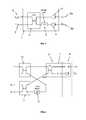
- FIG. 1is a schematic representation of a single sideband (SSB) modulator according to an embodiment of the invention
- FIG. 2is a schematic representation of a single sideband (SSB) modulator with means for suppressing the carrier according to an embodiment of the invention
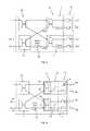
- FIG. 3is a schematic representation of a single sideband (SSB) modulator with an alternative means of suppressing the carrier and at the same time adding an independent sideband signal according to an embodiment of the invention.
- SSBsingle sideband
- FIG. 4is a schematic representation of a single sideband (SSB) modulator according to another embodiment of the invention.
- SSBsingle sideband
- FIG. 1illustrates a first embodiment of the optical single sideband modulator 1 employing reflection-mode optical intensity modulators 4 .
- the reflection-mode intensity modulatorscan be based on reflective electro-absorption-modulators (REAMs), an example of this technology is the R-EAM-1550 Reflective EAM manufactured by CIP Technologies of Ipswich, UK (www.ciphotonics.com/PDFs_March09/R_EAM — 1550_D.pdf).
- a continuous wave optical field E in (t)is applied to the input arm 5 of an optical coupler 2 that has a nominal power splitting/combining ratio of 50% (3 dB). The input light is split into two equal parts by the coupler 2 and guided to the reflective intensity modulators 4 .
- One of the partsis subjected to an optical phase shift 3 of ⁇ /4 radians on its journey towards the intensity modulator 4 and a further ⁇ /4 phase shift on its return.
- the net resultis a relative optical phase difference of ⁇ /2 radians between the reflected signals on the two arms.
- a message bearing electrical signal x(t) and its Hilbert transform x ⁇ (t)are applied (along with any dc bias voltages) to the electrical inputs 6 a , 6 b of the respective reflective intensity modulators 4 .
- E o (t)0.5 A ⁇ [ 1 +m ⁇ x ( t )] 0.5 ⁇ Cos( wt ) ⁇ [1 +m ⁇ x ⁇ ( t )] 0.5 ⁇ Sin( wt ) ⁇ (1)
- Ais the amplitude of the input field
- mis the intensity modulator modulation index.
- the square root termsare due to the intensity modulation process.
- An ideal 2 ⁇ 2 coupler scatter matrixwas used in deriving equation 1, see for example Agrawal, “Applications of Nonlinear Fiber Optics”, Academic Press 2001).
- Equation 3The first term in Equation 3 is the residual carrier and the other terms are the desired SSB signal.
- This type of SSB signalis called an SSB-TC where TC stands for transmitted carrier.
- the example SSB modulator described in FIG. 1 and by Equation 3is used to generate the upper sideband signal. However, by adjusting the electrical phases of the modulating signals on the electrical inputs 6 a and 6 b and/or by adjusting the optical phase 3 a lower sideband signal can be created.
- phase shift element 3may be implemented as a variable phase adjuster, based on a waveguide heater, as this offers an additional degree of freedom in setting the operating point of the SSB generator.
- the Hilbert transform of a signalis equivalent to applying a ⁇ /2 phase shift to all of the frequency components of the signal.
- the modulating signal x(t), and its Hilbert transform x ⁇ (t) at the electrical inputs 6 a , 6 bcan be virtually any type of information carrying waveform, ranging from a simple analogue or digital baseband signals, to a frequency division multiplex of many data signals. Applications range from point-to-point digital transmission systems to frequency division multiplexes of many data signals as used in cable access television (CATV) systems for example.
- CATVcable access television
- FIG. 2illustrates a second embodiment that can be used to suppress the optical carrier component shown in Equation 3.
- the input fieldis split into two parts by a coupler 10 , one part is sent to the SSB-TC generator 1 described previously in relation to FIG. 1 whilst the second part is subtracted from the SSB-TC signal at an output port coupler 11 to create an SSB suppressed carrier (SSB-SC) signal.
- Subtractionis accomplished in the coupler 11 by adjusting the phase of the carrier with the adjustable phase element 12 .
- the adjustable optical phase element 12could be placed on either input port to coupler 11 as all that matters is the relative phase of the two carriers when they combine in coupler 11 .
- phase 12When the phase 12 is correctly set to minimise the carrier on output port 13 the carrier will appear instead on output port 14 where it can be monitored as part of a feedback control system used to optimise the phase adjuster 12 .
- a variable optical attenuatorcould be placed in either output port of coupler 10 , or input port of coupler 11 , in order to allow the amplitudes of the two carriers to be balanced to give maximum carrier suppression when they are combined in anti-phase in coupler 11 .
- FIG. 2also shows how an array of reflective intensity modulators 8 can be assembled onto a common substrate for edge connecting to a Silica on Silicon planar waveguide structure 9 .
- FIG. 3illustrates a third embodiment that can be used to suppress the optical carrier and add an independently modulated lower sideband signal.
- the input signalis split into two parts by coupler 10 , each part is sent to an SSB-TC generator 1 and the corresponding SSB-TC output signals are combined in coupler 11 after one of the SSB-TC signals has been delayed by a phase adjuster 12 .
- the phase adjuster 12allows the relative phase of the carrier components of the two SSB-TC signals to be made ⁇ radians (180 degrees) out of phase so that they cancel on the output port 13 .
- the resultis two SSB-SC signals, one containing the upper sideband signals of message x 1 (t) and the other containing the lower sideband signals of message x 2 (t).
- the phase adjuster 12could be placed on either of SSB-TC generator 1 outputs as the objective is simply to create a ⁇ radians (180 degrees) phase shift on the carriers when they are combined in coupler 11 .
- the message signalscan be placed on the upper or the lower sidebands simply by adjusting the relative phase of their electrical drive signals 6 a and 6 b .
- the phase 12is correctly set to minimise the carrier on output port 13 the carrier will appear instead on output port 14 where it can be monitored as part of a feedback control system used to optimise the phase adjuster 12 .
- variable optical attenuatorcould be placed in either output port of coupler 10 , or input port of coupler 11 , in order to allow the amplitudes of the two carriers to be balanced to give maximum carrier suppression when they are combined in anti-phase in coupler 11 .
- FIG. 4illustrates an alternative embodiment of the optical single sideband modulator 1 based on a modified version of the SSB-SC modulator shown in FIG. 3 .
- the optical phase shift 3is set to give ⁇ /2 radians shift to the light on its journey towards the intensity modulator 4 and a further ⁇ /2 phase shift on its return.
- the net resultis a relative optical phase difference of ⁇ radians between the reflected signals on the two arms.
- a message bearing electrical signal x 1 (t)is applied at electrical input 6 a , its inverse ⁇ x 1 (t) is applied at electrical input 6 c , and the signal's Hilbert transform x ⁇ 1 (t) is applied at electrical input 6 b and its inverse x ⁇ 1 (t) is applied at electrical input 6 d (along with any dc bias voltages) to the reflective intensity modulators 4 .
- E iis the input optical field
- mis the intensity modulator modulation index.
- the square root termsare due to the intensity modulation process.
- An ideal 2 ⁇ 2 coupler scatter matrixwas used in deriving Equation 4, see for example Agrawal, “Applications of Nonlinear Fiber Optics”, Academic Press 2001.
- Equation 6only shows the series expansion terms up to powers of 3. Ignoring the higher order (odd harmonic) terms has negligible impact when the modulation depth m ⁇ 1, and all of the even order harmonics cancel anyway.
- Equation 9is immediately recognisable as the classic equation for an SSB signal.
- One sign of j ( ⁇ )corresponding to a lower side-band SSB signal, the other (+) corresponding to an upper side-band SSB signal.
- the two output ports 13 , 14will have opposite side-band SSB signals.
- the main difference between this result and that given earlier in Equation 3is that the carrier and all of the even-order harmonics have been eliminated.
- this improvement in signal qualityis achieved at the expense of reduced efficiency since only one SSB signal is generated on each output port.
- phase shift elements 3 and 12may be implemented as a variable phase adjuster, based on a waveguide heater, as this offers an additional degree of freedom in setting the operating point of the SSB generator.
Landscapes
- Physics & Mathematics (AREA)
- Engineering & Computer Science (AREA)
- Computer Networks & Wireless Communication (AREA)
- Signal Processing (AREA)
- Nonlinear Science (AREA)
- Optics & Photonics (AREA)
- Electromagnetism (AREA)
- General Physics & Mathematics (AREA)
- Optical Modulation, Optical Deflection, Nonlinear Optics, Optical Demodulation, Optical Logic Elements (AREA)
Abstract
Description
This application is a national phase of International Application No. PCT/GB2010/050463 filed Mar. 18, 2010 and published in the English language.
The invention relates to a device and method for modulating an optical carrier field with a single sideband signal. Applications exist in optical fibre telecommunications networks and optical fibre sensor networks.
It is well known that modulation formats generated electrically can be translated to optical frequencies by use of an optical single sideband (SSB) modulator. Because of the increased interest in the generation of more complex modulation formats to improve spectral efficiency there is a need for efficient and cost-effective methods for optical SSB modulation.
The usual method of generating optical SSB is to use one or more Mach-Zehnder Interferometer (MZI) arrangements. The arms of the MZI contain optical phase adjusters and electro-optic phase modulators. These are driven by a combination of electrical signals. The correct phase relationships to cancel (null) out the carrier and one set of sidebands is achieved using an appropriate combination of optical path lengths and control of the phase of the electrical drive signals. The resultant modulator is large (several cm long), often requiring special travelling-wave electrode structures, and is not well suited to optical integration in a photonic integrated circuit (PIC).
The present invention provides a device for modulating an optical carrier field with a single sideband signal as claimed inclaim 1 and a method as claimed inclaim 9. Optional features are described in the dependent claims.
According to the invention a much more compact architecture is possible, at least in preferred embodiments, based on optical intensity modulators (typically 100 um long) in the arms of a Michelson Interferometer. Reflection-mode electro-absorption modulators (REAMs), placed at the ends of each arm of the interferometer, may be driven by suitably phased electrical modulating signals. The relative optical path length of the two arms may be adjustable so that the correct optical phase relationship between the modulated optical carriers can be obtained. The Michelson Interferometer is inherently more compact than the MZI and is ideally suited to REAM technology. The small size, wide bandwidth, and low operating voltage of REAMs is also a major advantage for producing array devices suitable for PICs.
In broad terms, a method for generating an optical single sideband signal, the method comprising the steps of splitting an optical field into two parts and introducing a relative phase delay of +/−π/4 radians in each direction of transmission to one of the parts, intensity reflection-modulating each part with electrical signals having a relative phase delay of +/−π/2 radians and then recombining the reflection-modulated signals.
The reflection-modulators may be reflection electro-absorption modulators (R-EAMs). The optical splitting, combining and phase delay means may be performed by silica on silicon waveguides. The component parts may be assembled on a hybrid photonic integrated circuit.
The optical splitting, combining and phase delay means may be performed by indium phosphide waveguides. The component parts may be assembled on a monolithic photonic integrated circuit.
Additional optical splitters, combiners, and phase adjusters may be used to remove, or reduce, the optical carrier. The outputs of two single sideband modulators may be combined. A phase adjuster may be used to control the level of the carrier.
A number of single sideband generators or component parts may be combined on one or more hybrid or monolithic photonic integrated circuits.
There is also disclosed a feedback control system to optimise the residual optical carrier level by controlling the phase, and amplitude, of the component signals within the SSB generator.
Embodiments of the invention are further described hereinafter with reference to the accompanying drawings, in which:
Eo(t)=0.5A·{[1+m·x(t)]0.5·Cos(wt)−[1+m·x^(t)]0.5·Sin(wt)} (1)
where A is the amplitude of the input field and m is the intensity modulator modulation index. The square root terms are due to the intensity modulation process. An ideal 2×2 coupler scatter matrix was used in deriving
A series expansion of the square root terms ofEquation 1 gives:
Eo(t)=0.5A·{[1+m·x(t)/2−0.25m2x2(t)/2!+ - - - ]·Cos(wt)−[1+m·x^(t)/2−0.25m2x^2(t)/2!+ - - - ]·Sin(wt)} (2)
Eo(t)=0.5A·{[1+m·x(t)/2−0.25m2x2(t)/2!+ - - - ]·Cos(wt)−[1+m·x^(t)/2−0.25m2x^2(t)/2!+ - - - ]·Sin(wt)} (2)
For low modulation index (m<<1) higher order terms in the series expansion can be ignored and the output is approximated by:
Eo(t)˜(A/√2)·[Sin(wt−π/4)+m/(2√2)·{x(t)·Cos(wt)−x^(t)·Sin(wt)}] (3)
Eo(t)˜(A/√2)·[Sin(wt−π/4)+m/(2√2)·{x(t)·Cos(wt)−x^(t)·Sin(wt)}] (3)
The first term inEquation 3 is the residual carrier and the other terms are the desired SSB signal. This type of SSB signal is called an SSB-TC where TC stands for transmitted carrier. The example SSB modulator described inFIG. 1 and byEquation 3 is used to generate the upper sideband signal. However, by adjusting the electrical phases of the modulating signals on theelectrical inputs
Due to imperfections in the balance of the optical splitting/combining ratios of thecoupler 2 and differences in the optical path loss in the arms connecting the reflection modulators it may be desirable to adjust the electrical drive signal parameters, such as dc bias and modulating signal amplitude, in order to optimise the sideband suppression ratio. Thephase shift element 3 may be implemented as a variable phase adjuster, based on a waveguide heater, as this offers an additional degree of freedom in setting the operating point of the SSB generator.
The Hilbert transform of a signal is equivalent to applying a π/2 phase shift to all of the frequency components of the signal. The modulating signal x(t), and its Hilbert transform x^(t) at theelectrical inputs
A variable optical attenuator could be placed in either output port ofcoupler 10, or input port ofcoupler 11, in order to allow the amplitudes of the two carriers to be balanced to give maximum carrier suppression when they are combined in anti-phase incoupler 11.
The advantages of the proposed method of SSB generation are summarised below:
- Due to its reduced size, the reflection-mode architecture of the proposed SSB generator is better suited to photonic integrated circuit (PIC) implementations using either the hybrid or monolithic approaches to PIC fabrication.
- Reflection intensity modulators, such as R-EAMs, are very compact (˜100 um long) compared to optical phase modulators (˜1 cm long), have a wide-bandwidth (over 20 GHz) without having to resort to travelling wave electrode structures, and only require low drive voltages.
Eo(x1t)=0.5−3/2·Ei·{[1+m·x1(t)]0.5−[1−m·x1(t)]0.5} (4)
where Eiis the input optical field and m is the intensity modulator modulation index. The square root terms are due to the intensity modulation process. An ideal 2×2 coupler scatter matrix was used in deriving
Eo(x1t)=0.5−3/2·Ei·{[m·x1(t)]/2−[m·x1(t)]2/8+[m·x1(t)]3/16−+ - - - −[m·x1(t)]/2+[m·x1(t)]2/8−[m·x1(t)]3/16+− - - - } (5)
which simplifies further to . . .
Eo(x1t)=0.5−3/2·Ei·{[m·x1(t)]+[m·x1(t)]3/8+ - - - } (6)
The important observation here is that all of the even order harmonics cancel leaving only the odd order terms. Equation 6 only shows the series expansion terms up to powers of 3. Ignoring the higher order (odd harmonic) terms has negligible impact when the modulation depth m<1, and all of the even order harmonics cancel anyway.
Similarly, the resulting optical field Eo(t), at the output17 of thecoupler 2b, is now given by Equation 7:
Eo(x^1t)=0.5−3/2·Ei·{[m·x^1(t)]+[m·x^1(t)]3/8+ - - - } (7)
Eo(x^1t)=0.5−3/2·Ei·{[m·x^1(t)]+[m·x^1(t)]3/8+ - - - } (7)
The signals described byEquations 6 and 7 are combined incoupler 11 with a relative phase shift of φ radians due to thephase adjuster 12. If this phase difference is set to +/−π/2 radians, then the signals onoutput ports
Eo(t)=0.25·Ei·{[m·x1(t)]+[m·x1(t)]3/8+/−j·([m·x^1(t)]+[m·x^1(t)]3/8)} (8)
where j represents the square root of −1. One signal, corresponding to either +j or −j, will appear on one output port and the corresponding signal with opposite sign will appear on the other output port.
Eo(t)=0.25·Ei·{[m·x1(t)]+[m·x1(t)]3/8+/−j·([m·x^1(t)]+[m·x^1(t)]3/8)} (8)
where j represents the square root of −1. One signal, corresponding to either +j or −j, will appear on one output port and the corresponding signal with opposite sign will appear on the other output port.
For low modulation index (m<<1) higher order terms in the series expansion can be ignored and the output is approximated by:
Eo(t)˜0.25·Ei·{[m·x1(t)]+/−j·[m·x^1(t)]} (9)
Eo(t)˜0.25·Ei·{[m·x1(t)]+/−j·[m·x^1(t)]} (9)
Due to imperfections in the balance of the optical splitting/combining ratios of thecoupler 2 and differences in the optical path loss in the arms connecting the reflection modulators it may be desirable to adjust the electrical drive signal parameters, such as dc bias and modulating signal amplitude, in order to optimise the sideband suppression ratio. Thephase shift elements
Throughout the description and claims of this specification, the words “comprise” and “contain” and variations of them mean “including but not limited to”, and they are not intended to (and do not) exclude other components, integers or steps. Throughout the description and claims of this specification, the singular encompasses the plural unless the context otherwise requires. In particular, where the indefinite article is used, the specification is to be understood as contemplating plurality as well as singularity, unless the context requires otherwise.
Features, integers, characteristics or groups described in conjunction with a particular aspect, embodiment or example of the invention are to be understood to be applicable to any other aspect, embodiment or example described herein unless incompatible therewith. All of the features disclosed in this specification (including any accompanying claims, abstract and drawings), and/or all of the steps of any method or process so disclosed, may be combined in any combination, except combinations where at least some of such features and/or steps are mutually exclusive. The invention is not restricted to the details of any foregoing embodiments. The invention extends to any novel one, or any novel combination, of the features disclosed in this specification (including any accompanying claims, abstract and drawings), or to any novel one, or any novel combination, of the steps of any method or process so disclosed.
Claims (19)
1. A device for modulating an optical carrier field with a single sideband signal, the device comprising:
an optical input for an optical carrier signal;
an optical output for a modulated optical output signal;
a first optical splitter arranged to split the optical carrier signal into a first component signal and a second component signal;
a first reflection modulator arranged to intensity modulate the first component signal with only a first electrical signal;
a second reflection modulator arranged to intensity modulate only the second component signal with only a second electrical signal, the second electrical signal corresponding to the first electrical signal with a relative phase delay of +/−π/2 radians;
a first optical combiner arranged to recombine the modulated first component signal and the modulated second component signal to produce an optical output signal; and
a first phase delay arranged to apply a phase delay of +/−π/2 radians to one of the component signals before the component signals are recombined by the first optical combiner;
wherein the first optical splitter and the first optical combiner are disposed in a first coupler.
2. A device as claimed inclaim 1 , wherein the first phase delay is arranged to apply a phase delay of +/−π/4 radians to one of the component signals before reflection modulation and then to apply a phase delay of +/−π/4 radians to that component signal after reflection modulation.
3. A device as claimed inclaim 1 , further comprising
a second optical splitter interposed between the optical input and the first optical splitter, and
a second optical combiner interposed between the first optical combiner and the optical output, and
a second phase delay arranged to apply a phase delay to one input of the second optical combiner,
wherein the second optical splitter is arranged to split the optical carrier signal between the first optical splitter and the second optical combiner, the second optical combiner is arranged to combine the optical carrier signal at one of its inputs with the output of the first optical combiner at the other of its inputs, and the relative phase delay due to the second phase delay is configured to remove the optical carrier from the optical output signal at the optical output.
4. A device as claimed inclaim 3 , wherein the second optical combiner has two outputs, the first output for the optical output signal at the optical output of the device and wherein the device comprises a feedback mechanism which adjusts the phase delay applied by the second phase delay to maximise the optical carrier output at the second output of the second optical combiner.
5. A device as claimed inclaim 3 , wherein a second said device is interposed between the second optical splitter and the second optical combiner, whereby an input of the first optical splitter of the second device is connected to an output of the second optical splitter and an input of the second optical combiner is connected to an output of the first optical splitter of the second device.
6. A device as claimed inclaim 1 , further comprising:
a first additional optical splitter/combiner interposed between the first optical splitter and the first reflection modulator, the first additional optical splitter/combiner directing a portion of the first component signal to a first additional reflection modulator via a phase delay on both transmission and reflection of +/−π/2 radians,
a second additional optical splitter/combiner interposed between the second optical splitter and the second reflection modulator, the second additional optical splitter/combiner directing a portion of the second component signal to a second additional reflection modulator via a phase delay on both transmission and reflection of +/−π/2 radians,
wherein the combined output of the first additional optical splitter/combiner and the combiner output of the second additional splitter/combiner are combined by the first optical combiner, and
wherein the electrical signal applied to the first additional reflection modulator is inverse of the first electrical signal and the electrical signal applied to the second additional reflection modulator is inverse of the second electrical signal.
7. A device as claimed inclaim 6 , wherein the first phase delay is a variable phase delay.
8. A method for generating an optical single sideband signal, the method comprising the steps of splitting an optical field into two parts using a first coupler, intensity reflection-modulating each part with only one of two electrical signals, the two electrical signals having a relative phase delay of +/−π/2 radians, introducing a relative phase delay of +/−π/2 radians to one of the parts, and then recombining the reflection-modulated signals using the first coupler.
9. A method as claimed inclaim 8 , wherein the step of introducing a relative phase delay to one of the parts comprises introducing a relative phase delay of +/−π/4 radians in each direction of transmission (pre- and post-reflection modulation) to the said part.
10. A method as claimed inclaim 8 , wherein the reflection-modulation step uses reflection electro-absorption modulators (R-EAMs).
11. A method as claimed inclaim 8 , wherein the optical splitting, recombining and phase delaying are performed by silica on silicon waveguides.
12. A method as claimed inclaim 8 , wherein the optical splitting, recombining and phase delaying are performed by indium phosphide waveguides.
13. A method as claimed inclaim 8 , wherein the component parts are assembled on a hybrid photonic integrated circuit.
14. A method as claimed inclaim 13 , wherein the component parts are assembled on a monolithic photonic integrated circuit.
15. A method as claimed inclaim 8 , comprising removing or reducing an optical carrier using at least an additional optical splitter, combiner, and phase adjuster.
16. A method as claimed inclaim 15 further comprising controlling the phase and amplitude of the combined signals by means of feedback to optimise removal of the optical earner.
17. A method as claimed inclaim 8 , wherein the outputs of two single sideband modulators are combined.
18. A method as claimed inclaim 17 , wherein a phase adjuster is used to control a level of the carrier.
19. A method as claimed inclaim 8 , wherein a plurality of single sideband generators or component parts are combined on one or more hybrid or monolithic photonic integrated circuits.
Applications Claiming Priority (3)
| Application Number | Priority Date | Filing Date | Title |
|---|---|---|---|
| GB0904600.4 | 2009-03-18 | ||
| GBGB0904600.4AGB0904600D0 (en) | 2009-03-18 | 2009-03-18 | Optical single-sideband transmitter |
| PCT/GB2010/050463WO2010106368A1 (en) | 2009-03-18 | 2010-03-18 | Optical single-sideband transmitter |
Publications (2)
| Publication Number | Publication Date |
|---|---|
| US20120002978A1 US20120002978A1 (en) | 2012-01-05 |
| US8824900B2true US8824900B2 (en) | 2014-09-02 |
Family
ID=40637503
Family Applications (1)
| Application Number | Title | Priority Date | Filing Date |
|---|---|---|---|
| US13/256,861Active2030-06-02US8824900B2 (en) | 2009-03-18 | 2010-03-18 | Optical single-sideband transmitter |
Country Status (5)
| Country | Link |
|---|---|
| US (1) | US8824900B2 (en) |
| EP (1) | EP2409430B1 (en) |
| CN (1) | CN102356572B (en) |
| GB (1) | GB0904600D0 (en) |
| WO (1) | WO2010106368A1 (en) |
Families Citing this family (10)
| Publication number | Priority date | Publication date | Assignee | Title |
|---|---|---|---|---|
| GB201100194D0 (en)* | 2011-01-07 | 2011-02-23 | Cip Technologies Ltd | Optical duobinary transmitter |
| CN102680211B (en)* | 2012-05-28 | 2015-01-14 | 中国电子科技集团公司第四十一研究所 | Method for testing polarization coupling strength of polarization maintaining optical fiber based on polarization beam-splitting interference technique |
| CN103078682B (en)* | 2012-12-31 | 2018-02-06 | 青岛农业大学 | Optical carrier-to-sideband ratio self-adapting optical fiber wireless single-sideband modulation system |
| CN103439806A (en)* | 2013-08-06 | 2013-12-11 | 浙江大学 | Reflective thermo-optic variable optical attenuator |
| US9507238B2 (en)* | 2014-08-21 | 2016-11-29 | Morton Photonics | Linearized Bragg grating assisted electro-optic modulator |
| WO2017177372A1 (en)* | 2016-04-12 | 2017-10-19 | 华为技术有限公司 | Device and method for generating optical signal, and chip |
| US10411807B1 (en)* | 2018-04-05 | 2019-09-10 | Nokia Solutions And Networks Oy | Optical transmitter having an array of surface-coupled electro-absorption modulators |
| US10727948B2 (en) | 2018-04-05 | 2020-07-28 | Nokia Solutions And Networks Oy | Communication system employing surface-coupled optical devices |
| US11139894B2 (en)* | 2019-10-22 | 2021-10-05 | Nokia Solutions And Networks Oy | Data transmission on phase components of an optical carrier by direct modulation of reflectors of a laser |
| US12407409B2 (en)* | 2023-06-26 | 2025-09-02 | Raytheon Company | Single-sideband reduced-carrier phase-shifting electro-optic modulator |
Citations (17)
| Publication number | Priority date | Publication date | Assignee | Title |
|---|---|---|---|---|
| US3379887A (en) | 1965-12-01 | 1968-04-23 | Gen Dynamics Corp | Electro-optical modulator |
| US4257016A (en)* | 1979-02-21 | 1981-03-17 | Xerox Corporation | Piezo-optic, total internal reflection modulator |
| US4915468A (en) | 1987-02-20 | 1990-04-10 | The Board Of Trustees Of The Leland Stanford Junior University | Apparatus using two-mode optical waveguide with non-circular core |
| US5155617A (en)* | 1991-06-13 | 1992-10-13 | The Board Of Trustees Of The Leland Stanford Junior University | Electro-optic attenuated total internal reflection modulator and method |
| US6275625B1 (en)* | 1999-03-17 | 2001-08-14 | Agere Systems Optoelectronics Guardian Corp. | Optical mirror switch using a michelson interferometer |
| US20020141694A1 (en)* | 2001-03-15 | 2002-10-03 | Massachusetts Institute Of Technology | Methods of achieving optimal communications performance |
| US20020149826A1 (en)* | 2001-02-15 | 2002-10-17 | Kikuji Tanaka | Optical single-sideband modulated signal generator |
| US20020171900A1 (en)* | 2001-03-02 | 2002-11-21 | Nec Corporation | Method and circuit for generating single-sideband optical signal |
| US6616353B1 (en)* | 1999-10-07 | 2003-09-09 | Massachusetts Institute Of Technology | Laser intensity noise suppression using unbalanced interferometer modulation |
| US20030189745A1 (en) | 2002-04-05 | 2003-10-09 | Nobuhiko Kikuchi | Optical single sideband transmitter |
| US20040228635A1 (en) | 2001-08-24 | 2004-11-18 | Corvis Corporation | Optical transmission systems, devices, and method |
| US20050254061A1 (en)* | 2004-05-14 | 2005-11-17 | Alphonse Gerard A | Low coherence interferometry for detecting and characterizing plaques |
| US20070047668A1 (en) | 2005-09-01 | 2007-03-01 | Samsung Electronics Co., Ltd. | Single side band modulator module and single side band modulator device using the same |
| US20070212075A1 (en) | 2006-03-09 | 2007-09-13 | Yy Labs, Inc. | Dual-parallel-mz modulator bias control |
| US20090022445A1 (en)* | 2005-06-28 | 2009-01-22 | California Institute Of Technology | Nanophotonic devices in silicon |
| US20090067843A1 (en)* | 2007-07-17 | 2009-03-12 | Way Winston I | Optical Wavelength-Division-Multiplexed (WDM) Comb Generator Using a Single Laser |
| US7570409B1 (en)* | 2006-10-12 | 2009-08-04 | Hewlett-Packard Development Company, L.P. | Radiation modulation by reflection from controlled composite material |
- 2009
- 2009-03-18GBGBGB0904600.4Apatent/GB0904600D0/ennot_activeCeased
- 2010
- 2010-03-18WOPCT/GB2010/050463patent/WO2010106368A1/enactiveApplication Filing
- 2010-03-18USUS13/256,861patent/US8824900B2/enactiveActive
- 2010-03-18CNCN201080012577.4Apatent/CN102356572B/enactiveActive
- 2010-03-18EPEP10711453Apatent/EP2409430B1/enactiveActive
Patent Citations (17)
| Publication number | Priority date | Publication date | Assignee | Title |
|---|---|---|---|---|
| US3379887A (en) | 1965-12-01 | 1968-04-23 | Gen Dynamics Corp | Electro-optical modulator |
| US4257016A (en)* | 1979-02-21 | 1981-03-17 | Xerox Corporation | Piezo-optic, total internal reflection modulator |
| US4915468A (en) | 1987-02-20 | 1990-04-10 | The Board Of Trustees Of The Leland Stanford Junior University | Apparatus using two-mode optical waveguide with non-circular core |
| US5155617A (en)* | 1991-06-13 | 1992-10-13 | The Board Of Trustees Of The Leland Stanford Junior University | Electro-optic attenuated total internal reflection modulator and method |
| US6275625B1 (en)* | 1999-03-17 | 2001-08-14 | Agere Systems Optoelectronics Guardian Corp. | Optical mirror switch using a michelson interferometer |
| US6616353B1 (en)* | 1999-10-07 | 2003-09-09 | Massachusetts Institute Of Technology | Laser intensity noise suppression using unbalanced interferometer modulation |
| US20020149826A1 (en)* | 2001-02-15 | 2002-10-17 | Kikuji Tanaka | Optical single-sideband modulated signal generator |
| US20020171900A1 (en)* | 2001-03-02 | 2002-11-21 | Nec Corporation | Method and circuit for generating single-sideband optical signal |
| US20020141694A1 (en)* | 2001-03-15 | 2002-10-03 | Massachusetts Institute Of Technology | Methods of achieving optimal communications performance |
| US20040228635A1 (en) | 2001-08-24 | 2004-11-18 | Corvis Corporation | Optical transmission systems, devices, and method |
| US20030189745A1 (en) | 2002-04-05 | 2003-10-09 | Nobuhiko Kikuchi | Optical single sideband transmitter |
| US20050254061A1 (en)* | 2004-05-14 | 2005-11-17 | Alphonse Gerard A | Low coherence interferometry for detecting and characterizing plaques |
| US20090022445A1 (en)* | 2005-06-28 | 2009-01-22 | California Institute Of Technology | Nanophotonic devices in silicon |
| US20070047668A1 (en) | 2005-09-01 | 2007-03-01 | Samsung Electronics Co., Ltd. | Single side band modulator module and single side band modulator device using the same |
| US20070212075A1 (en) | 2006-03-09 | 2007-09-13 | Yy Labs, Inc. | Dual-parallel-mz modulator bias control |
| US7570409B1 (en)* | 2006-10-12 | 2009-08-04 | Hewlett-Packard Development Company, L.P. | Radiation modulation by reflection from controlled composite material |
| US20090067843A1 (en)* | 2007-07-17 | 2009-03-12 | Way Winston I | Optical Wavelength-Division-Multiplexed (WDM) Comb Generator Using a Single Laser |
Non-Patent Citations (4)
| Title |
|---|
| Chinese Search Report received in Application No. 2010800125774, mailed Aug. 6, 2013, 2 pages. |
| International Search Report corresponding to International Application No. PCT/GB2010/050463 dated Jun. 15, 2010. |
| Presi et al., "A full-duplex symmetric WDM-PON featuring OSSB downlink modulation with optical down-conversion", Optical Fiber Communication/National Fiber Optic Engineers Conference, Feb. 24, 2008, pp. 1-3. |
| Written Opnion and Search Report of the International Searching Authority received in Patent Cooperation Treaty Application No. PCT/GB2010/050463, mailed Jun. 22, 2010, 7 pages. |
Also Published As
| Publication number | Publication date |
|---|---|
| US20120002978A1 (en) | 2012-01-05 |
| CN102356572B (en) | 2015-03-11 |
| CN102356572A (en) | 2012-02-15 |
| GB0904600D0 (en) | 2009-04-29 |
| EP2409430B1 (en) | 2013-03-06 |
| EP2409430A1 (en) | 2012-01-25 |
| WO2010106368A1 (en) | 2010-09-23 |
Similar Documents
| Publication | Publication Date | Title |
|---|---|---|
| US8824900B2 (en) | Optical single-sideband transmitter | |
| US8295710B2 (en) | Optical I-Q-modulator | |
| CN107247381B (en) | A kind of integrated arbitrary waveform signal generator of silicon substrate | |
| US20090214224A1 (en) | Method and apparatus for coherent analog rf photonic transmission | |
| US9312962B2 (en) | Intensity-based modulator | |
| JP6540952B2 (en) | Method of generating optical two-tone signal and control method of DP-MZM type light modulator | |
| JPH1152313A (en) | Light modulator | |
| JP4878358B2 (en) | Optical SSB modulator | |
| JP5594192B2 (en) | Light modulator | |
| Mazur et al. | Optical frequency comb modulator for multichannel systems | |
| US6535316B1 (en) | Generation of high-speed digital optical signals | |
| JPH10206661A (en) | Polarization scrambler and optical integrated circuit using the same | |
| CN117240368B (en) | Optical domain spectrum synthesis system and optical domain spectrum synthesis method | |
| JP2003348022A (en) | Optical transmitter | |
| JP2001159750A (en) | Optical transmitter and optical modulator | |
| JP6547116B2 (en) | Light modulator | |
| JP6911483B2 (en) | Wavelength converter, controlled light generator, wavelength conversion method, and controlled light generator | |
| Talkhooncheh et al. | A 200gb/s qam-16 silicon photonic transmitter with 4 binary-driven eams in an mzi structure | |
| JP4434688B2 (en) | Light modulator | |
| US20020080454A1 (en) | Method, system and apparatus for optically transferring information | |
| JP2008228206A (en) | Optical angle modulator | |
| CN116137548B (en) | Harmonic generator, harmonic modulation component, optical module and optical communication device | |
| JP7541270B2 (en) | Optical modulation circuit and digital signal processing method | |
| JP2824420B2 (en) | Light modulator | |
| EP2659602B1 (en) | An optical duobinary modulated signal generator |
Legal Events
| Date | Code | Title | Description |
|---|---|---|---|
| AS | Assignment | Owner name:THE CENTRE FOR INTEGRATED PHOTONICS LIMITED, UNITE Free format text:ASSIGNMENT OF ASSIGNORS INTEREST;ASSIGNORS:HEALEY, PETER;SMITH, DAVID WILLIAM;MAXWELL, GRAEME DOUGLAS;REEL/FRAME:026917/0053 Effective date:20110915 | |
| AS | Assignment | Owner name:HUAWEI TECHNOLOGIES CO., LTD., CHINA Free format text:ASSIGNMENT OF ASSIGNORS INTEREST;ASSIGNOR:THE CENTRE FOR INTEGRATED PHOTONICS LIMITED;REEL/FRAME:028471/0850 Effective date:20120607 | |
| STCF | Information on status: patent grant | Free format text:PATENTED CASE | |
| MAFP | Maintenance fee payment | Free format text:PAYMENT OF MAINTENANCE FEE, 4TH YEAR, LARGE ENTITY (ORIGINAL EVENT CODE: M1551) Year of fee payment:4 | |
| MAFP | Maintenance fee payment | Free format text:PAYMENT OF MAINTENANCE FEE, 8TH YEAR, LARGE ENTITY (ORIGINAL EVENT CODE: M1552); ENTITY STATUS OF PATENT OWNER: LARGE ENTITY Year of fee payment:8 |