US8823165B2 - Memory module in a package - Google Patents
Memory module in a packageDownload PDFInfo
- Publication number
- US8823165B2 US8823165B2US13/346,185US201213346185AUS8823165B2US 8823165 B2US8823165 B2US 8823165B2US 201213346185 AUS201213346185 AUS 201213346185AUS 8823165 B2US8823165 B2US 8823165B2
- Authority
- US
- United States
- Prior art keywords
- microelectronic
- package
- elements
- contacts
- microelectronic package
- Prior art date
- Legal status (The legal status is an assumption and is not a legal conclusion. Google has not performed a legal analysis and makes no representation as to the accuracy of the status listed.)
- Active, expires
Links
Images


Classifications
- H—ELECTRICITY
- H01—ELECTRIC ELEMENTS
- H01L—SEMICONDUCTOR DEVICES NOT COVERED BY CLASS H10
- H01L23/00—Details of semiconductor or other solid state devices
- H01L23/48—Arrangements for conducting electric current to or from the solid state body in operation, e.g. leads, terminal arrangements ; Selection of materials therefor
- H01L23/481—Internal lead connections, e.g. via connections, feedthrough structures
- G—PHYSICS
- G11—INFORMATION STORAGE
- G11C—STATIC STORES
- G11C5/00—Details of stores covered by group G11C11/00
- G11C5/02—Disposition of storage elements, e.g. in the form of a matrix array
- G11C5/04—Supports for storage elements, e.g. memory modules; Mounting or fixing of storage elements on such supports
- H—ELECTRICITY
- H01—ELECTRIC ELEMENTS
- H01L—SEMICONDUCTOR DEVICES NOT COVERED BY CLASS H10
- H01L23/00—Details of semiconductor or other solid state devices
- H01L23/12—Mountings, e.g. non-detachable insulating substrates
- H—ELECTRICITY
- H01—ELECTRIC ELEMENTS
- H01L—SEMICONDUCTOR DEVICES NOT COVERED BY CLASS H10
- H01L23/00—Details of semiconductor or other solid state devices
- H01L23/52—Arrangements for conducting electric current within the device in operation from one component to another, i.e. interconnections, e.g. wires, lead frames
- H01L23/538—Arrangements for conducting electric current within the device in operation from one component to another, i.e. interconnections, e.g. wires, lead frames the interconnection structure between a plurality of semiconductor chips being formed on, or in, insulating substrates
- H01L23/5386—Geometry or layout of the interconnection structure
- H—ELECTRICITY
- H01—ELECTRIC ELEMENTS
- H01L—SEMICONDUCTOR DEVICES NOT COVERED BY CLASS H10
- H01L24/00—Arrangements for connecting or disconnecting semiconductor or solid-state bodies; Methods or apparatus related thereto
- H01L24/01—Means for bonding being attached to, or being formed on, the surface to be connected, e.g. chip-to-package, die-attach, "first-level" interconnects; Manufacturing methods related thereto
- H01L24/02—Bonding areas ; Manufacturing methods related thereto
- H01L24/04—Structure, shape, material or disposition of the bonding areas prior to the connecting process
- H01L24/06—Structure, shape, material or disposition of the bonding areas prior to the connecting process of a plurality of bonding areas
- H—ELECTRICITY
- H01—ELECTRIC ELEMENTS
- H01L—SEMICONDUCTOR DEVICES NOT COVERED BY CLASS H10
- H01L24/00—Arrangements for connecting or disconnecting semiconductor or solid-state bodies; Methods or apparatus related thereto
- H01L24/01—Means for bonding being attached to, or being formed on, the surface to be connected, e.g. chip-to-package, die-attach, "first-level" interconnects; Manufacturing methods related thereto
- H01L24/02—Bonding areas ; Manufacturing methods related thereto
- H01L24/07—Structure, shape, material or disposition of the bonding areas after the connecting process
- H01L24/09—Structure, shape, material or disposition of the bonding areas after the connecting process of a plurality of bonding areas
- H—ELECTRICITY
- H01—ELECTRIC ELEMENTS
- H01L—SEMICONDUCTOR DEVICES NOT COVERED BY CLASS H10
- H01L25/00—Assemblies consisting of a plurality of semiconductor or other solid state devices
- H01L25/03—Assemblies consisting of a plurality of semiconductor or other solid state devices all the devices being of a type provided for in a single subclass of subclasses H10B, H10D, H10F, H10H, H10K or H10N, e.g. assemblies of rectifier diodes
- H01L25/04—Assemblies consisting of a plurality of semiconductor or other solid state devices all the devices being of a type provided for in a single subclass of subclasses H10B, H10D, H10F, H10H, H10K or H10N, e.g. assemblies of rectifier diodes the devices not having separate containers
- H01L25/065—Assemblies consisting of a plurality of semiconductor or other solid state devices all the devices being of a type provided for in a single subclass of subclasses H10B, H10D, H10F, H10H, H10K or H10N, e.g. assemblies of rectifier diodes the devices not having separate containers the devices being of a type provided for in group H10D89/00
- H01L25/0652—Assemblies consisting of a plurality of semiconductor or other solid state devices all the devices being of a type provided for in a single subclass of subclasses H10B, H10D, H10F, H10H, H10K or H10N, e.g. assemblies of rectifier diodes the devices not having separate containers the devices being of a type provided for in group H10D89/00 the devices being arranged next and on each other, i.e. mixed assemblies
- H—ELECTRICITY
- H01—ELECTRIC ELEMENTS
- H01L—SEMICONDUCTOR DEVICES NOT COVERED BY CLASS H10
- H01L25/00—Assemblies consisting of a plurality of semiconductor or other solid state devices
- H01L25/18—Assemblies consisting of a plurality of semiconductor or other solid state devices the devices being of the types provided for in two or more different main groups of the same subclass of H10B, H10D, H10F, H10H, H10K or H10N
- H—ELECTRICITY
- H10—SEMICONDUCTOR DEVICES; ELECTRIC SOLID-STATE DEVICES NOT OTHERWISE PROVIDED FOR
- H10B—ELECTRONIC MEMORY DEVICES
- H10B12/00—Dynamic random access memory [DRAM] devices
- H—ELECTRICITY
- H01—ELECTRIC ELEMENTS
- H01L—SEMICONDUCTOR DEVICES NOT COVERED BY CLASS H10
- H01L2224/00—Indexing scheme for arrangements for connecting or disconnecting semiconductor or solid-state bodies and methods related thereto as covered by H01L24/00
- H01L2224/01—Means for bonding being attached to, or being formed on, the surface to be connected, e.g. chip-to-package, die-attach, "first-level" interconnects; Manufacturing methods related thereto
- H01L2224/02—Bonding areas; Manufacturing methods related thereto
- H01L2224/04—Structure, shape, material or disposition of the bonding areas prior to the connecting process
- H01L2224/0401—Bonding areas specifically adapted for bump connectors, e.g. under bump metallisation [UBM]
- H—ELECTRICITY
- H01—ELECTRIC ELEMENTS
- H01L—SEMICONDUCTOR DEVICES NOT COVERED BY CLASS H10
- H01L2224/00—Indexing scheme for arrangements for connecting or disconnecting semiconductor or solid-state bodies and methods related thereto as covered by H01L24/00
- H01L2224/01—Means for bonding being attached to, or being formed on, the surface to be connected, e.g. chip-to-package, die-attach, "first-level" interconnects; Manufacturing methods related thereto
- H01L2224/02—Bonding areas; Manufacturing methods related thereto
- H01L2224/04—Structure, shape, material or disposition of the bonding areas prior to the connecting process
- H01L2224/06—Structure, shape, material or disposition of the bonding areas prior to the connecting process of a plurality of bonding areas
- H01L2224/061—Disposition
- H—ELECTRICITY
- H01—ELECTRIC ELEMENTS
- H01L—SEMICONDUCTOR DEVICES NOT COVERED BY CLASS H10
- H01L2224/00—Indexing scheme for arrangements for connecting or disconnecting semiconductor or solid-state bodies and methods related thereto as covered by H01L24/00
- H01L2224/01—Means for bonding being attached to, or being formed on, the surface to be connected, e.g. chip-to-package, die-attach, "first-level" interconnects; Manufacturing methods related thereto
- H01L2224/02—Bonding areas; Manufacturing methods related thereto
- H01L2224/07—Structure, shape, material or disposition of the bonding areas after the connecting process
- H01L2224/09—Structure, shape, material or disposition of the bonding areas after the connecting process of a plurality of bonding areas
- H01L2224/091—Disposition
- H—ELECTRICITY
- H01—ELECTRIC ELEMENTS
- H01L—SEMICONDUCTOR DEVICES NOT COVERED BY CLASS H10
- H01L2224/00—Indexing scheme for arrangements for connecting or disconnecting semiconductor or solid-state bodies and methods related thereto as covered by H01L24/00
- H01L2224/01—Means for bonding being attached to, or being formed on, the surface to be connected, e.g. chip-to-package, die-attach, "first-level" interconnects; Manufacturing methods related thereto
- H01L2224/10—Bump connectors; Manufacturing methods related thereto
- H01L2224/15—Structure, shape, material or disposition of the bump connectors after the connecting process
- H01L2224/16—Structure, shape, material or disposition of the bump connectors after the connecting process of an individual bump connector
- H01L2224/161—Disposition
- H01L2224/16151—Disposition the bump connector connecting between a semiconductor or solid-state body and an item not being a semiconductor or solid-state body, e.g. chip-to-substrate, chip-to-passive
- H01L2224/16221—Disposition the bump connector connecting between a semiconductor or solid-state body and an item not being a semiconductor or solid-state body, e.g. chip-to-substrate, chip-to-passive the body and the item being stacked
- H01L2224/16225—Disposition the bump connector connecting between a semiconductor or solid-state body and an item not being a semiconductor or solid-state body, e.g. chip-to-substrate, chip-to-passive the body and the item being stacked the item being non-metallic, e.g. insulating substrate with or without metallisation
- H01L2224/16227—Disposition the bump connector connecting between a semiconductor or solid-state body and an item not being a semiconductor or solid-state body, e.g. chip-to-substrate, chip-to-passive the body and the item being stacked the item being non-metallic, e.g. insulating substrate with or without metallisation the bump connector connecting to a bond pad of the item
- H—ELECTRICITY
- H01—ELECTRIC ELEMENTS
- H01L—SEMICONDUCTOR DEVICES NOT COVERED BY CLASS H10
- H01L2224/00—Indexing scheme for arrangements for connecting or disconnecting semiconductor or solid-state bodies and methods related thereto as covered by H01L24/00
- H01L2224/01—Means for bonding being attached to, or being formed on, the surface to be connected, e.g. chip-to-package, die-attach, "first-level" interconnects; Manufacturing methods related thereto
- H01L2224/26—Layer connectors, e.g. plate connectors, solder or adhesive layers; Manufacturing methods related thereto
- H01L2224/28—Structure, shape, material or disposition of the layer connectors prior to the connecting process
- H01L2224/29—Structure, shape, material or disposition of the layer connectors prior to the connecting process of an individual layer connector
- H01L2224/29001—Core members of the layer connector
- H01L2224/29099—Material
- H01L2224/291—Material with a principal constituent of the material being a metal or a metalloid, e.g. boron [B], silicon [Si], germanium [Ge], arsenic [As], antimony [Sb], tellurium [Te] and polonium [Po], and alloys thereof
- H—ELECTRICITY
- H01—ELECTRIC ELEMENTS
- H01L—SEMICONDUCTOR DEVICES NOT COVERED BY CLASS H10
- H01L2224/00—Indexing scheme for arrangements for connecting or disconnecting semiconductor or solid-state bodies and methods related thereto as covered by H01L24/00
- H01L2224/01—Means for bonding being attached to, or being formed on, the surface to be connected, e.g. chip-to-package, die-attach, "first-level" interconnects; Manufacturing methods related thereto
- H01L2224/26—Layer connectors, e.g. plate connectors, solder or adhesive layers; Manufacturing methods related thereto
- H01L2224/28—Structure, shape, material or disposition of the layer connectors prior to the connecting process
- H01L2224/29—Structure, shape, material or disposition of the layer connectors prior to the connecting process of an individual layer connector
- H01L2224/29001—Core members of the layer connector
- H01L2224/29099—Material
- H01L2224/2919—Material with a principal constituent of the material being a polymer, e.g. polyester, phenolic based polymer, epoxy
- H—ELECTRICITY
- H01—ELECTRIC ELEMENTS
- H01L—SEMICONDUCTOR DEVICES NOT COVERED BY CLASS H10
- H01L2224/00—Indexing scheme for arrangements for connecting or disconnecting semiconductor or solid-state bodies and methods related thereto as covered by H01L24/00
- H01L2224/01—Means for bonding being attached to, or being formed on, the surface to be connected, e.g. chip-to-package, die-attach, "first-level" interconnects; Manufacturing methods related thereto
- H01L2224/26—Layer connectors, e.g. plate connectors, solder or adhesive layers; Manufacturing methods related thereto
- H01L2224/28—Structure, shape, material or disposition of the layer connectors prior to the connecting process
- H01L2224/29—Structure, shape, material or disposition of the layer connectors prior to the connecting process of an individual layer connector
- H01L2224/29001—Core members of the layer connector
- H01L2224/29099—Material
- H01L2224/29193—Material with a principal constituent of the material being a solid not provided for in groups H01L2224/291 - H01L2224/29191, e.g. allotropes of carbon, fullerene, graphite, carbon-nanotubes, diamond
- H—ELECTRICITY
- H01—ELECTRIC ELEMENTS
- H01L—SEMICONDUCTOR DEVICES NOT COVERED BY CLASS H10
- H01L2224/00—Indexing scheme for arrangements for connecting or disconnecting semiconductor or solid-state bodies and methods related thereto as covered by H01L24/00
- H01L2224/01—Means for bonding being attached to, or being formed on, the surface to be connected, e.g. chip-to-package, die-attach, "first-level" interconnects; Manufacturing methods related thereto
- H01L2224/26—Layer connectors, e.g. plate connectors, solder or adhesive layers; Manufacturing methods related thereto
- H01L2224/31—Structure, shape, material or disposition of the layer connectors after the connecting process
- H01L2224/32—Structure, shape, material or disposition of the layer connectors after the connecting process of an individual layer connector
- H01L2224/321—Disposition
- H01L2224/32135—Disposition the layer connector connecting between different semiconductor or solid-state bodies, i.e. chip-to-chip
- H01L2224/32145—Disposition the layer connector connecting between different semiconductor or solid-state bodies, i.e. chip-to-chip the bodies being stacked
- H—ELECTRICITY
- H01—ELECTRIC ELEMENTS
- H01L—SEMICONDUCTOR DEVICES NOT COVERED BY CLASS H10
- H01L2224/00—Indexing scheme for arrangements for connecting or disconnecting semiconductor or solid-state bodies and methods related thereto as covered by H01L24/00
- H01L2224/01—Means for bonding being attached to, or being formed on, the surface to be connected, e.g. chip-to-package, die-attach, "first-level" interconnects; Manufacturing methods related thereto
- H01L2224/26—Layer connectors, e.g. plate connectors, solder or adhesive layers; Manufacturing methods related thereto
- H01L2224/31—Structure, shape, material or disposition of the layer connectors after the connecting process
- H01L2224/32—Structure, shape, material or disposition of the layer connectors after the connecting process of an individual layer connector
- H01L2224/321—Disposition
- H01L2224/32151—Disposition the layer connector connecting between a semiconductor or solid-state body and an item not being a semiconductor or solid-state body, e.g. chip-to-substrate, chip-to-passive
- H01L2224/32221—Disposition the layer connector connecting between a semiconductor or solid-state body and an item not being a semiconductor or solid-state body, e.g. chip-to-substrate, chip-to-passive the body and the item being stacked
- H01L2224/32225—Disposition the layer connector connecting between a semiconductor or solid-state body and an item not being a semiconductor or solid-state body, e.g. chip-to-substrate, chip-to-passive the body and the item being stacked the item being non-metallic, e.g. insulating substrate with or without metallisation
- H—ELECTRICITY
- H01—ELECTRIC ELEMENTS
- H01L—SEMICONDUCTOR DEVICES NOT COVERED BY CLASS H10
- H01L2224/00—Indexing scheme for arrangements for connecting or disconnecting semiconductor or solid-state bodies and methods related thereto as covered by H01L24/00
- H01L2224/01—Means for bonding being attached to, or being formed on, the surface to be connected, e.g. chip-to-package, die-attach, "first-level" interconnects; Manufacturing methods related thereto
- H01L2224/42—Wire connectors; Manufacturing methods related thereto
- H01L2224/47—Structure, shape, material or disposition of the wire connectors after the connecting process
- H01L2224/48—Structure, shape, material or disposition of the wire connectors after the connecting process of an individual wire connector
- H01L2224/481—Disposition
- H01L2224/48135—Connecting between different semiconductor or solid-state bodies, i.e. chip-to-chip
- H01L2224/48145—Connecting between different semiconductor or solid-state bodies, i.e. chip-to-chip the bodies being stacked
- H—ELECTRICITY
- H01—ELECTRIC ELEMENTS
- H01L—SEMICONDUCTOR DEVICES NOT COVERED BY CLASS H10
- H01L2224/00—Indexing scheme for arrangements for connecting or disconnecting semiconductor or solid-state bodies and methods related thereto as covered by H01L24/00
- H01L2224/01—Means for bonding being attached to, or being formed on, the surface to be connected, e.g. chip-to-package, die-attach, "first-level" interconnects; Manufacturing methods related thereto
- H01L2224/42—Wire connectors; Manufacturing methods related thereto
- H01L2224/47—Structure, shape, material or disposition of the wire connectors after the connecting process
- H01L2224/48—Structure, shape, material or disposition of the wire connectors after the connecting process of an individual wire connector
- H01L2224/481—Disposition
- H01L2224/48151—Connecting between a semiconductor or solid-state body and an item not being a semiconductor or solid-state body, e.g. chip-to-substrate, chip-to-passive
- H01L2224/48221—Connecting between a semiconductor or solid-state body and an item not being a semiconductor or solid-state body, e.g. chip-to-substrate, chip-to-passive the body and the item being stacked
- H01L2224/48225—Connecting between a semiconductor or solid-state body and an item not being a semiconductor or solid-state body, e.g. chip-to-substrate, chip-to-passive the body and the item being stacked the item being non-metallic, e.g. insulating substrate with or without metallisation
- H01L2224/48227—Connecting between a semiconductor or solid-state body and an item not being a semiconductor or solid-state body, e.g. chip-to-substrate, chip-to-passive the body and the item being stacked the item being non-metallic, e.g. insulating substrate with or without metallisation connecting the wire to a bond pad of the item
- H—ELECTRICITY
- H01—ELECTRIC ELEMENTS
- H01L—SEMICONDUCTOR DEVICES NOT COVERED BY CLASS H10
- H01L2224/00—Indexing scheme for arrangements for connecting or disconnecting semiconductor or solid-state bodies and methods related thereto as covered by H01L24/00
- H01L2224/01—Means for bonding being attached to, or being formed on, the surface to be connected, e.g. chip-to-package, die-attach, "first-level" interconnects; Manufacturing methods related thereto
- H01L2224/42—Wire connectors; Manufacturing methods related thereto
- H01L2224/47—Structure, shape, material or disposition of the wire connectors after the connecting process
- H01L2224/48—Structure, shape, material or disposition of the wire connectors after the connecting process of an individual wire connector
- H01L2224/481—Disposition
- H01L2224/48151—Connecting between a semiconductor or solid-state body and an item not being a semiconductor or solid-state body, e.g. chip-to-substrate, chip-to-passive
- H01L2224/48221—Connecting between a semiconductor or solid-state body and an item not being a semiconductor or solid-state body, e.g. chip-to-substrate, chip-to-passive the body and the item being stacked
- H01L2224/48225—Connecting between a semiconductor or solid-state body and an item not being a semiconductor or solid-state body, e.g. chip-to-substrate, chip-to-passive the body and the item being stacked the item being non-metallic, e.g. insulating substrate with or without metallisation
- H01L2224/4824—Connecting between the body and an opposite side of the item with respect to the body
- H—ELECTRICITY
- H01—ELECTRIC ELEMENTS
- H01L—SEMICONDUCTOR DEVICES NOT COVERED BY CLASS H10
- H01L2224/00—Indexing scheme for arrangements for connecting or disconnecting semiconductor or solid-state bodies and methods related thereto as covered by H01L24/00
- H01L2224/73—Means for bonding being of different types provided for in two or more of groups H01L2224/10, H01L2224/18, H01L2224/26, H01L2224/34, H01L2224/42, H01L2224/50, H01L2224/63, H01L2224/71
- H01L2224/732—Location after the connecting process
- H01L2224/73201—Location after the connecting process on the same surface
- H01L2224/73203—Bump and layer connectors
- H01L2224/73204—Bump and layer connectors the bump connector being embedded into the layer connector
- H—ELECTRICITY
- H01—ELECTRIC ELEMENTS
- H01L—SEMICONDUCTOR DEVICES NOT COVERED BY CLASS H10
- H01L2224/00—Indexing scheme for arrangements for connecting or disconnecting semiconductor or solid-state bodies and methods related thereto as covered by H01L24/00
- H01L2224/73—Means for bonding being of different types provided for in two or more of groups H01L2224/10, H01L2224/18, H01L2224/26, H01L2224/34, H01L2224/42, H01L2224/50, H01L2224/63, H01L2224/71
- H01L2224/732—Location after the connecting process
- H01L2224/73201—Location after the connecting process on the same surface
- H01L2224/73215—Layer and wire connectors
- H—ELECTRICITY
- H01—ELECTRIC ELEMENTS
- H01L—SEMICONDUCTOR DEVICES NOT COVERED BY CLASS H10
- H01L2224/00—Indexing scheme for arrangements for connecting or disconnecting semiconductor or solid-state bodies and methods related thereto as covered by H01L24/00
- H01L2224/73—Means for bonding being of different types provided for in two or more of groups H01L2224/10, H01L2224/18, H01L2224/26, H01L2224/34, H01L2224/42, H01L2224/50, H01L2224/63, H01L2224/71
- H01L2224/732—Location after the connecting process
- H01L2224/73251—Location after the connecting process on different surfaces
- H01L2224/73253—Bump and layer connectors
- H—ELECTRICITY
- H01—ELECTRIC ELEMENTS
- H01L—SEMICONDUCTOR DEVICES NOT COVERED BY CLASS H10
- H01L2224/00—Indexing scheme for arrangements for connecting or disconnecting semiconductor or solid-state bodies and methods related thereto as covered by H01L24/00
- H01L2224/73—Means for bonding being of different types provided for in two or more of groups H01L2224/10, H01L2224/18, H01L2224/26, H01L2224/34, H01L2224/42, H01L2224/50, H01L2224/63, H01L2224/71
- H01L2224/732—Location after the connecting process
- H01L2224/73251—Location after the connecting process on different surfaces
- H01L2224/73265—Layer and wire connectors
- H—ELECTRICITY
- H01—ELECTRIC ELEMENTS
- H01L—SEMICONDUCTOR DEVICES NOT COVERED BY CLASS H10
- H01L2225/00—Details relating to assemblies covered by the group H01L25/00 but not provided for in its subgroups
- H01L2225/03—All the devices being of a type provided for in the same main group of the same subclass of class H10, e.g. assemblies of rectifier diodes
- H01L2225/04—All the devices being of a type provided for in the same main group of the same subclass of class H10, e.g. assemblies of rectifier diodes the devices not having separate containers
- H01L2225/065—All the devices being of a type provided for in the same main group of the same subclass of class H10
- H01L2225/06503—Stacked arrangements of devices
- H01L2225/06506—Wire or wire-like electrical connections between devices
- H—ELECTRICITY
- H01—ELECTRIC ELEMENTS
- H01L—SEMICONDUCTOR DEVICES NOT COVERED BY CLASS H10
- H01L2225/00—Details relating to assemblies covered by the group H01L25/00 but not provided for in its subgroups
- H01L2225/03—All the devices being of a type provided for in the same main group of the same subclass of class H10, e.g. assemblies of rectifier diodes
- H01L2225/04—All the devices being of a type provided for in the same main group of the same subclass of class H10, e.g. assemblies of rectifier diodes the devices not having separate containers
- H01L2225/065—All the devices being of a type provided for in the same main group of the same subclass of class H10
- H01L2225/06503—Stacked arrangements of devices
- H01L2225/0651—Wire or wire-like electrical connections from device to substrate
- H—ELECTRICITY
- H01—ELECTRIC ELEMENTS
- H01L—SEMICONDUCTOR DEVICES NOT COVERED BY CLASS H10
- H01L2225/00—Details relating to assemblies covered by the group H01L25/00 but not provided for in its subgroups
- H01L2225/03—All the devices being of a type provided for in the same main group of the same subclass of class H10, e.g. assemblies of rectifier diodes
- H01L2225/04—All the devices being of a type provided for in the same main group of the same subclass of class H10, e.g. assemblies of rectifier diodes the devices not having separate containers
- H01L2225/065—All the devices being of a type provided for in the same main group of the same subclass of class H10
- H01L2225/06503—Stacked arrangements of devices
- H01L2225/06517—Bump or bump-like direct electrical connections from device to substrate
- H—ELECTRICITY
- H01—ELECTRIC ELEMENTS
- H01L—SEMICONDUCTOR DEVICES NOT COVERED BY CLASS H10
- H01L2225/00—Details relating to assemblies covered by the group H01L25/00 but not provided for in its subgroups
- H01L2225/03—All the devices being of a type provided for in the same main group of the same subclass of class H10, e.g. assemblies of rectifier diodes
- H01L2225/04—All the devices being of a type provided for in the same main group of the same subclass of class H10, e.g. assemblies of rectifier diodes the devices not having separate containers
- H01L2225/065—All the devices being of a type provided for in the same main group of the same subclass of class H10
- H01L2225/06503—Stacked arrangements of devices
- H01L2225/06541—Conductive via connections through the device, e.g. vertical interconnects, through silicon via [TSV]
- H—ELECTRICITY
- H01—ELECTRIC ELEMENTS
- H01L—SEMICONDUCTOR DEVICES NOT COVERED BY CLASS H10
- H01L2225/00—Details relating to assemblies covered by the group H01L25/00 but not provided for in its subgroups
- H01L2225/03—All the devices being of a type provided for in the same main group of the same subclass of class H10, e.g. assemblies of rectifier diodes
- H01L2225/04—All the devices being of a type provided for in the same main group of the same subclass of class H10, e.g. assemblies of rectifier diodes the devices not having separate containers
- H01L2225/065—All the devices being of a type provided for in the same main group of the same subclass of class H10
- H01L2225/06503—Stacked arrangements of devices
- H01L2225/06555—Geometry of the stack, e.g. form of the devices, geometry to facilitate stacking
- H01L2225/06562—Geometry of the stack, e.g. form of the devices, geometry to facilitate stacking at least one device in the stack being rotated or offset
- H—ELECTRICITY
- H01—ELECTRIC ELEMENTS
- H01L—SEMICONDUCTOR DEVICES NOT COVERED BY CLASS H10
- H01L2225/00—Details relating to assemblies covered by the group H01L25/00 but not provided for in its subgroups
- H01L2225/03—All the devices being of a type provided for in the same main group of the same subclass of class H10, e.g. assemblies of rectifier diodes
- H01L2225/04—All the devices being of a type provided for in the same main group of the same subclass of class H10, e.g. assemblies of rectifier diodes the devices not having separate containers
- H01L2225/065—All the devices being of a type provided for in the same main group of the same subclass of class H10
- H01L2225/06503—Stacked arrangements of devices
- H01L2225/06589—Thermal management, e.g. cooling
- H—ELECTRICITY
- H01—ELECTRIC ELEMENTS
- H01L—SEMICONDUCTOR DEVICES NOT COVERED BY CLASS H10
- H01L23/00—Details of semiconductor or other solid state devices
- H01L23/12—Mountings, e.g. non-detachable insulating substrates
- H01L23/13—Mountings, e.g. non-detachable insulating substrates characterised by the shape
- H—ELECTRICITY
- H01—ELECTRIC ELEMENTS
- H01L—SEMICONDUCTOR DEVICES NOT COVERED BY CLASS H10
- H01L23/00—Details of semiconductor or other solid state devices
- H01L23/28—Encapsulations, e.g. encapsulating layers, coatings, e.g. for protection
- H01L23/31—Encapsulations, e.g. encapsulating layers, coatings, e.g. for protection characterised by the arrangement or shape
- H01L23/3107—Encapsulations, e.g. encapsulating layers, coatings, e.g. for protection characterised by the arrangement or shape the device being completely enclosed
- H01L23/3121—Encapsulations, e.g. encapsulating layers, coatings, e.g. for protection characterised by the arrangement or shape the device being completely enclosed a substrate forming part of the encapsulation
- H01L23/3128—Encapsulations, e.g. encapsulating layers, coatings, e.g. for protection characterised by the arrangement or shape the device being completely enclosed a substrate forming part of the encapsulation the substrate having spherical bumps for external connection
- H—ELECTRICITY
- H01—ELECTRIC ELEMENTS
- H01L—SEMICONDUCTOR DEVICES NOT COVERED BY CLASS H10
- H01L23/00—Details of semiconductor or other solid state devices
- H01L23/34—Arrangements for cooling, heating, ventilating or temperature compensation ; Temperature sensing arrangements
- H01L23/36—Selection of materials, or shaping, to facilitate cooling or heating, e.g. heatsinks
- H—ELECTRICITY
- H01—ELECTRIC ELEMENTS
- H01L—SEMICONDUCTOR DEVICES NOT COVERED BY CLASS H10
- H01L23/00—Details of semiconductor or other solid state devices
- H01L23/48—Arrangements for conducting electric current to or from the solid state body in operation, e.g. leads, terminal arrangements ; Selection of materials therefor
- H01L23/488—Arrangements for conducting electric current to or from the solid state body in operation, e.g. leads, terminal arrangements ; Selection of materials therefor consisting of soldered or bonded constructions
- H01L23/498—Leads, i.e. metallisations or lead-frames on insulating substrates, e.g. chip carriers
- H01L23/49838—Geometry or layout
- H—ELECTRICITY
- H01—ELECTRIC ELEMENTS
- H01L—SEMICONDUCTOR DEVICES NOT COVERED BY CLASS H10
- H01L24/00—Arrangements for connecting or disconnecting semiconductor or solid-state bodies; Methods or apparatus related thereto
- H01L24/01—Means for bonding being attached to, or being formed on, the surface to be connected, e.g. chip-to-package, die-attach, "first-level" interconnects; Manufacturing methods related thereto
- H01L24/26—Layer connectors, e.g. plate connectors, solder or adhesive layers; Manufacturing methods related thereto
- H01L24/28—Structure, shape, material or disposition of the layer connectors prior to the connecting process
- H01L24/29—Structure, shape, material or disposition of the layer connectors prior to the connecting process of an individual layer connector
- H—ELECTRICITY
- H01—ELECTRIC ELEMENTS
- H01L—SEMICONDUCTOR DEVICES NOT COVERED BY CLASS H10
- H01L24/00—Arrangements for connecting or disconnecting semiconductor or solid-state bodies; Methods or apparatus related thereto
- H01L24/01—Means for bonding being attached to, or being formed on, the surface to be connected, e.g. chip-to-package, die-attach, "first-level" interconnects; Manufacturing methods related thereto
- H01L24/42—Wire connectors; Manufacturing methods related thereto
- H01L24/47—Structure, shape, material or disposition of the wire connectors after the connecting process
- H01L24/48—Structure, shape, material or disposition of the wire connectors after the connecting process of an individual wire connector
- H—ELECTRICITY
- H01—ELECTRIC ELEMENTS
- H01L—SEMICONDUCTOR DEVICES NOT COVERED BY CLASS H10
- H01L24/00—Arrangements for connecting or disconnecting semiconductor or solid-state bodies; Methods or apparatus related thereto
- H01L24/73—Means for bonding being of different types provided for in two or more of groups H01L24/10, H01L24/18, H01L24/26, H01L24/34, H01L24/42, H01L24/50, H01L24/63, H01L24/71
- H—ELECTRICITY
- H01—ELECTRIC ELEMENTS
- H01L—SEMICONDUCTOR DEVICES NOT COVERED BY CLASS H10
- H01L25/00—Assemblies consisting of a plurality of semiconductor or other solid state devices
- H01L25/03—Assemblies consisting of a plurality of semiconductor or other solid state devices all the devices being of a type provided for in a single subclass of subclasses H10B, H10D, H10F, H10H, H10K or H10N, e.g. assemblies of rectifier diodes
- H01L25/04—Assemblies consisting of a plurality of semiconductor or other solid state devices all the devices being of a type provided for in a single subclass of subclasses H10B, H10D, H10F, H10H, H10K or H10N, e.g. assemblies of rectifier diodes the devices not having separate containers
- H01L25/065—Assemblies consisting of a plurality of semiconductor or other solid state devices all the devices being of a type provided for in a single subclass of subclasses H10B, H10D, H10F, H10H, H10K or H10N, e.g. assemblies of rectifier diodes the devices not having separate containers the devices being of a type provided for in group H10D89/00
- H01L25/0655—Assemblies consisting of a plurality of semiconductor or other solid state devices all the devices being of a type provided for in a single subclass of subclasses H10B, H10D, H10F, H10H, H10K or H10N, e.g. assemblies of rectifier diodes the devices not having separate containers the devices being of a type provided for in group H10D89/00 the devices being arranged next to each other
- H—ELECTRICITY
- H01—ELECTRIC ELEMENTS
- H01L—SEMICONDUCTOR DEVICES NOT COVERED BY CLASS H10
- H01L25/00—Assemblies consisting of a plurality of semiconductor or other solid state devices
- H01L25/03—Assemblies consisting of a plurality of semiconductor or other solid state devices all the devices being of a type provided for in a single subclass of subclasses H10B, H10D, H10F, H10H, H10K or H10N, e.g. assemblies of rectifier diodes
- H01L25/04—Assemblies consisting of a plurality of semiconductor or other solid state devices all the devices being of a type provided for in a single subclass of subclasses H10B, H10D, H10F, H10H, H10K or H10N, e.g. assemblies of rectifier diodes the devices not having separate containers
- H01L25/065—Assemblies consisting of a plurality of semiconductor or other solid state devices all the devices being of a type provided for in a single subclass of subclasses H10B, H10D, H10F, H10H, H10K or H10N, e.g. assemblies of rectifier diodes the devices not having separate containers the devices being of a type provided for in group H10D89/00
- H01L25/0657—Stacked arrangements of devices
- H—ELECTRICITY
- H01—ELECTRIC ELEMENTS
- H01L—SEMICONDUCTOR DEVICES NOT COVERED BY CLASS H10
- H01L2924/00—Indexing scheme for arrangements or methods for connecting or disconnecting semiconductor or solid-state bodies as covered by H01L24/00
- H01L2924/0001—Technical content checked by a classifier
- H01L2924/00014—Technical content checked by a classifier the subject-matter covered by the group, the symbol of which is combined with the symbol of this group, being disclosed without further technical details
- H—ELECTRICITY
- H01—ELECTRIC ELEMENTS
- H01L—SEMICONDUCTOR DEVICES NOT COVERED BY CLASS H10
- H01L2924/00—Indexing scheme for arrangements or methods for connecting or disconnecting semiconductor or solid-state bodies as covered by H01L24/00
- H01L2924/013—Alloys
- H01L2924/0132—Binary Alloys
- H01L2924/01322—Eutectic Alloys, i.e. obtained by a liquid transforming into two solid phases
- H—ELECTRICITY
- H01—ELECTRIC ELEMENTS
- H01L—SEMICONDUCTOR DEVICES NOT COVERED BY CLASS H10
- H01L2924/00—Indexing scheme for arrangements or methods for connecting or disconnecting semiconductor or solid-state bodies as covered by H01L24/00
- H01L2924/10—Details of semiconductor or other solid state devices to be connected
- H01L2924/11—Device type
- H01L2924/12—Passive devices, e.g. 2 terminal devices
- H01L2924/1203—Rectifying Diode
- H—ELECTRICITY
- H01—ELECTRIC ELEMENTS
- H01L—SEMICONDUCTOR DEVICES NOT COVERED BY CLASS H10
- H01L2924/00—Indexing scheme for arrangements or methods for connecting or disconnecting semiconductor or solid-state bodies as covered by H01L24/00
- H01L2924/10—Details of semiconductor or other solid state devices to be connected
- H01L2924/11—Device type
- H01L2924/12—Passive devices, e.g. 2 terminal devices
- H01L2924/1205—Capacitor
- H—ELECTRICITY
- H01—ELECTRIC ELEMENTS
- H01L—SEMICONDUCTOR DEVICES NOT COVERED BY CLASS H10
- H01L2924/00—Indexing scheme for arrangements or methods for connecting or disconnecting semiconductor or solid-state bodies as covered by H01L24/00
- H01L2924/10—Details of semiconductor or other solid state devices to be connected
- H01L2924/11—Device type
- H01L2924/14—Integrated circuits
- H01L2924/143—Digital devices
- H01L2924/1431—Logic devices
- H—ELECTRICITY
- H01—ELECTRIC ELEMENTS
- H01L—SEMICONDUCTOR DEVICES NOT COVERED BY CLASS H10
- H01L2924/00—Indexing scheme for arrangements or methods for connecting or disconnecting semiconductor or solid-state bodies as covered by H01L24/00
- H01L2924/10—Details of semiconductor or other solid state devices to be connected
- H01L2924/11—Device type
- H01L2924/14—Integrated circuits
- H01L2924/143—Digital devices
- H01L2924/1432—Central processing unit [CPU]
- H—ELECTRICITY
- H01—ELECTRIC ELEMENTS
- H01L—SEMICONDUCTOR DEVICES NOT COVERED BY CLASS H10
- H01L2924/00—Indexing scheme for arrangements or methods for connecting or disconnecting semiconductor or solid-state bodies as covered by H01L24/00
- H01L2924/10—Details of semiconductor or other solid state devices to be connected
- H01L2924/11—Device type
- H01L2924/14—Integrated circuits
- H01L2924/143—Digital devices
- H01L2924/1433—Application-specific integrated circuit [ASIC]
- H—ELECTRICITY
- H01—ELECTRIC ELEMENTS
- H01L—SEMICONDUCTOR DEVICES NOT COVERED BY CLASS H10
- H01L2924/00—Indexing scheme for arrangements or methods for connecting or disconnecting semiconductor or solid-state bodies as covered by H01L24/00
- H01L2924/10—Details of semiconductor or other solid state devices to be connected
- H01L2924/11—Device type
- H01L2924/14—Integrated circuits
- H01L2924/143—Digital devices
- H01L2924/14335—Digital signal processor [DSP]
- H—ELECTRICITY
- H01—ELECTRIC ELEMENTS
- H01L—SEMICONDUCTOR DEVICES NOT COVERED BY CLASS H10
- H01L2924/00—Indexing scheme for arrangements or methods for connecting or disconnecting semiconductor or solid-state bodies as covered by H01L24/00
- H01L2924/10—Details of semiconductor or other solid state devices to be connected
- H01L2924/11—Device type
- H01L2924/14—Integrated circuits
- H01L2924/143—Digital devices
- H01L2924/1434—Memory
- H01L2924/1435—Random access memory [RAM]
- H01L2924/1436—Dynamic random-access memory [DRAM]
- H—ELECTRICITY
- H01—ELECTRIC ELEMENTS
- H01L—SEMICONDUCTOR DEVICES NOT COVERED BY CLASS H10
- H01L2924/00—Indexing scheme for arrangements or methods for connecting or disconnecting semiconductor or solid-state bodies as covered by H01L24/00
- H01L2924/10—Details of semiconductor or other solid state devices to be connected
- H01L2924/11—Device type
- H01L2924/14—Integrated circuits
- H01L2924/143—Digital devices
- H01L2924/1434—Memory
- H01L2924/1435—Random access memory [RAM]
- H01L2924/1438—Flash memory
- H—ELECTRICITY
- H01—ELECTRIC ELEMENTS
- H01L—SEMICONDUCTOR DEVICES NOT COVERED BY CLASS H10
- H01L2924/00—Indexing scheme for arrangements or methods for connecting or disconnecting semiconductor or solid-state bodies as covered by H01L24/00
- H01L2924/10—Details of semiconductor or other solid state devices to be connected
- H01L2924/11—Device type
- H01L2924/14—Integrated circuits
- H01L2924/143—Digital devices
- H01L2924/1434—Memory
- H01L2924/1435—Random access memory [RAM]
- H01L2924/1443—Non-volatile random-access memory [NVRAM]
- H—ELECTRICITY
- H01—ELECTRIC ELEMENTS
- H01L—SEMICONDUCTOR DEVICES NOT COVERED BY CLASS H10
- H01L2924/00—Indexing scheme for arrangements or methods for connecting or disconnecting semiconductor or solid-state bodies as covered by H01L24/00
- H01L2924/15—Details of package parts other than the semiconductor or other solid state devices to be connected
- H01L2924/151—Die mounting substrate
- H01L2924/153—Connection portion
- H01L2924/1531—Connection portion the connection portion being formed only on the surface of the substrate opposite to the die mounting surface
- H01L2924/15311—Connection portion the connection portion being formed only on the surface of the substrate opposite to the die mounting surface being a ball array, e.g. BGA
- H—ELECTRICITY
- H01—ELECTRIC ELEMENTS
- H01L—SEMICONDUCTOR DEVICES NOT COVERED BY CLASS H10
- H01L2924/00—Indexing scheme for arrangements or methods for connecting or disconnecting semiconductor or solid-state bodies as covered by H01L24/00
- H01L2924/15—Details of package parts other than the semiconductor or other solid state devices to be connected
- H01L2924/151—Die mounting substrate
- H01L2924/153—Connection portion
- H01L2924/1531—Connection portion the connection portion being formed only on the surface of the substrate opposite to the die mounting surface
- H01L2924/15312—Connection portion the connection portion being formed only on the surface of the substrate opposite to the die mounting surface being a pin array, e.g. PGA
- H—ELECTRICITY
- H01—ELECTRIC ELEMENTS
- H01L—SEMICONDUCTOR DEVICES NOT COVERED BY CLASS H10
- H01L2924/00—Indexing scheme for arrangements or methods for connecting or disconnecting semiconductor or solid-state bodies as covered by H01L24/00
- H01L2924/15—Details of package parts other than the semiconductor or other solid state devices to be connected
- H01L2924/151—Die mounting substrate
- H01L2924/153—Connection portion
- H01L2924/1531—Connection portion the connection portion being formed only on the surface of the substrate opposite to the die mounting surface
- H01L2924/15313—Connection portion the connection portion being formed only on the surface of the substrate opposite to the die mounting surface being a land array, e.g. LGA
- H—ELECTRICITY
- H01—ELECTRIC ELEMENTS
- H01L—SEMICONDUCTOR DEVICES NOT COVERED BY CLASS H10
- H01L2924/00—Indexing scheme for arrangements or methods for connecting or disconnecting semiconductor or solid-state bodies as covered by H01L24/00
- H01L2924/15—Details of package parts other than the semiconductor or other solid state devices to be connected
- H01L2924/151—Die mounting substrate
- H01L2924/156—Material
- H01L2924/157—Material with a principal constituent of the material being a metal or a metalloid, e.g. boron [B], silicon [Si], germanium [Ge], arsenic [As], antimony [Sb], tellurium [Te] and polonium [Po], and alloys thereof
- H—ELECTRICITY
- H01—ELECTRIC ELEMENTS
- H01L—SEMICONDUCTOR DEVICES NOT COVERED BY CLASS H10
- H01L2924/00—Indexing scheme for arrangements or methods for connecting or disconnecting semiconductor or solid-state bodies as covered by H01L24/00
- H01L2924/15—Details of package parts other than the semiconductor or other solid state devices to be connected
- H01L2924/151—Die mounting substrate
- H01L2924/156—Material
- H01L2924/15786—Material with a principal constituent of the material being a non metallic, non metalloid inorganic material
- H01L2924/15787—Ceramics, e.g. crystalline carbides, nitrides or oxides
- H—ELECTRICITY
- H01—ELECTRIC ELEMENTS
- H01L—SEMICONDUCTOR DEVICES NOT COVERED BY CLASS H10
- H01L2924/00—Indexing scheme for arrangements or methods for connecting or disconnecting semiconductor or solid-state bodies as covered by H01L24/00
- H01L2924/15—Details of package parts other than the semiconductor or other solid state devices to be connected
- H01L2924/151—Die mounting substrate
- H01L2924/156—Material
- H01L2924/15786—Material with a principal constituent of the material being a non metallic, non metalloid inorganic material
- H01L2924/15788—Glasses, e.g. amorphous oxides, nitrides or fluorides
- H—ELECTRICITY
- H01—ELECTRIC ELEMENTS
- H01L—SEMICONDUCTOR DEVICES NOT COVERED BY CLASS H10
- H01L2924/00—Indexing scheme for arrangements or methods for connecting or disconnecting semiconductor or solid-state bodies as covered by H01L24/00
- H01L2924/15—Details of package parts other than the semiconductor or other solid state devices to be connected
- H01L2924/151—Die mounting substrate
- H01L2924/156—Material
- H01L2924/1579—Material with a principal constituent of the material being a polymer, e.g. polyester, phenolic based polymer, epoxy
- H—ELECTRICITY
- H01—ELECTRIC ELEMENTS
- H01L—SEMICONDUCTOR DEVICES NOT COVERED BY CLASS H10
- H01L2924/00—Indexing scheme for arrangements or methods for connecting or disconnecting semiconductor or solid-state bodies as covered by H01L24/00
- H01L2924/15—Details of package parts other than the semiconductor or other solid state devices to be connected
- H01L2924/181—Encapsulation
- H01L2924/1815—Shape
- H01L2924/1816—Exposing the passive side of the semiconductor or solid-state body
- H01L2924/18161—Exposing the passive side of the semiconductor or solid-state body of a flip chip
- H—ELECTRICITY
- H01—ELECTRIC ELEMENTS
- H01L—SEMICONDUCTOR DEVICES NOT COVERED BY CLASS H10
- H01L2924/00—Indexing scheme for arrangements or methods for connecting or disconnecting semiconductor or solid-state bodies as covered by H01L24/00
- H01L2924/15—Details of package parts other than the semiconductor or other solid state devices to be connected
- H01L2924/181—Encapsulation
- H01L2924/1815—Shape
- H01L2924/1816—Exposing the passive side of the semiconductor or solid-state body
- H01L2924/18165—Exposing the passive side of the semiconductor or solid-state body of a wire bonded chip
- H—ELECTRICITY
- H01—ELECTRIC ELEMENTS
- H01L—SEMICONDUCTOR DEVICES NOT COVERED BY CLASS H10
- H01L2924/00—Indexing scheme for arrangements or methods for connecting or disconnecting semiconductor or solid-state bodies as covered by H01L24/00
- H01L2924/19—Details of hybrid assemblies other than the semiconductor or other solid state devices to be connected
- H01L2924/1901—Structure
- H01L2924/1904—Component type
- H01L2924/19041—Component type being a capacitor
- H—ELECTRICITY
- H01—ELECTRIC ELEMENTS
- H01L—SEMICONDUCTOR DEVICES NOT COVERED BY CLASS H10
- H01L2924/00—Indexing scheme for arrangements or methods for connecting or disconnecting semiconductor or solid-state bodies as covered by H01L24/00
- H01L2924/19—Details of hybrid assemblies other than the semiconductor or other solid state devices to be connected
- H01L2924/191—Disposition
- H01L2924/19101—Disposition of discrete passive components
- H01L2924/19105—Disposition of discrete passive components in a side-by-side arrangement on a common die mounting substrate
- H—ELECTRICITY
- H01—ELECTRIC ELEMENTS
- H01L—SEMICONDUCTOR DEVICES NOT COVERED BY CLASS H10
- H01L2924/00—Indexing scheme for arrangements or methods for connecting or disconnecting semiconductor or solid-state bodies as covered by H01L24/00
- H01L2924/30—Technical effects
- H01L2924/301—Electrical effects
Definitions
- the subject matter of the present applicationrelates to microelectronic packages and assemblies incorporating microelectronic packages.
- a standard chiphas a flat, rectangular body with a large front face having contacts connected to the internal circuitry of the chip.
- Each individual chiptypically is contained in a package having external terminals connected to the contacts of the chip.
- the terminalsi.e., the external connection points of the package, are configured to electrically connect to a circuit panel, such as a printed circuit board.
- the chip packageoccupies an area of the circuit panel considerably larger than the area of the chip itself.
- the “area of the chip”should be understood as referring to the area of the front face.
- flip chipdesigns, the front face of the chip confronts the face of a package dielectric element, i.e., substrate of the package, and the contacts on the chip are bonded directly to contacts on the face of the substrate by solder bumps or other connecting elements.
- the substratecan be bonded to a circuit panel through the external terminals that overlie the substrate.
- the “flip chip” designprovides a relatively compact arrangement; each package occupies an area of the circuit panel equal to or slightly larger than the area of the chip's front face, such as disclosed, for example, in certain embodiments of commonly-assigned U.S. Pat. Nos. 5,148,265; 5,148,266; and 5,679,977, the disclosures of which are incorporated herein by reference.
- Certain innovative mounting techniquesoffer compactness approaching or equal to that of conventional flip-chip bonding.
- Packages that can accommodate a single chip in an area of the circuit panel equal to or slightly larger than the area of the chip itselfare commonly referred to as “chip-scale packages.”
- Sizeis a significant consideration in any physical arrangement of chips.
- devices commonly referred to as “smart phones”integrate the functions of a cellular telephone with powerful data processors, memory and ancillary devices such as global positioning system receivers, electronic cameras, and local area network connections along with high-resolution displays and associated image processing chips.
- Such devicescan provide capabilities such as full internet connectivity, entertainment including full-resolution video, navigation, electronic banking and more, all in a pocket-size device.
- Complex portable devicesrequire packing numerous chips into a small space.
- I/Osinput and output connections
- the components that form the interconnectionsshould not greatly increase the size of the assembly. Similar needs arise in other applications as, for example, in data servers such as those used in internet search engines where increased performance and size reduction are needed.
- DRAMsdynamic random access memory chips
- flash memory chipsare commonly packaged in single-chip or multiple-chip packages and assemblies.
- Each packagehas many electrical connections for carrying signals, power and ground between terminals and the chips therein.
- the electrical connectionscan include different kinds of conductors such as horizontal conductors, e.g., traces, beam leads, etc., which extend in a horizontal direction relative to a contact-bearing surface of a chip, vertical conductors such as vias, which extend in a vertical direction relative to the surface of the chip, and wire bonds that extend in both horizontal and vertical directions relative to the surface of the chip.
- the transmission of signals within packages to chips of multi-chip packagesposes particular challenges, especially for signals common to two or more chips in the package such as clock signals, and address and strobe signals for memory chips.
- the lengths of the connection paths between the terminals of the package and the chipscan vary. The different path lengths can cause the signals to take longer or shorter times to travel between the terminals and each chip. Travel time of a signal from one point to another is called “propagation delay” and is a function of the conductor length, the conductor's structure, and other dielectric or conductive structure in close proximity therewith.
- skewDifferences in the times at which two different signals reach a particular location can also be called “skew”.
- the skew in the arrival times of a particular signal at two or more locationsis a result of both propagation delay and the times at which the particular signal starts to travel towards the locations.
- Skewmay or may not impact circuit performance. Skew often has little impact on performance when all signals in a synchronous group of signals are skewed together, in which case all signals needed for operation arrive together when needed. However, this is not the case when different signals of a group of synchronous signals needed for operation arrive at different times. In this case the skew impacts performance because the operation cannot be performed unless all needed signals have arrived.
- the embodiments described hereincan include features that minimize skew that are disclosed in the copending U.S. Provisional Patent Application No. 61/506,889 (TESSERA 3.8-664), the disclosure of which is incorporated by reference herein.
- microelectronic packagescan incorporate a microelectronic element that is configured to predominantly provide memory storage array function, i.e., a microelectronic element that embodies a greater number of active devices to provide memory storage array function than any other function.
- the microelectronic elementmay be or include a DRAM chip, or a stacked electrically interconnected assembly of such semiconductor chips.
- all of the terminals of such packageare placed in sets of columns adjacent to one or more peripheral edges of a package substrate to which the microelectronic element is mounted.
- a microelectronic packagecan include a substrate having first and second opposed surfaces, at least two pairs of microelectronic elements, each pair of microelectronic elements including an upper microelectronic element and a lower microelectronic element, a plurality of terminals exposed at the second surface, and electrical connections extending from at least some of contacts of each lower microelectronic element to at least some of the terminals.
- the pairs of microelectronic elementscan be fully spaced apart from one another in a horizontal direction parallel to the first surface of the substrate.
- Each lower microelectronic elementcan have a front surface facing the first surface of the substrate and a plurality of contacts at the front surface.
- the front surfaces of the lower microelectronic elementscan be arranged in a single plane parallel to the first surface.
- a surface of each of the upper microelectronic elementscan at least partially overlie a rear surface of the lower microelectronic element in its pair.
- the microelectronic elementscan together be configured to predominantly provide memory storage array function.
- the terminalscan be configured for connecting the microelectronic package to at least one component external to the microelectronic package.
- At least some of the plurality of contacts of the lower microelectronic element of first and second ones of the pairs of microelectronic elementscan be arranged in a respective column of contacts defining respective first and second axes.
- the first and second axescan be transverse to one another.
- the first and second axescan be orthogonal to one another.
- at least some of the plurality of contacts of the lower microelectronic element of first and second ones of the pairs of microelectronic elementscan be arranged in a respective column of contacts defining respective first and second axes.
- the first and second axescan be parallel to one another.
- the at least two pairs of microelectronic elementscan include four pairs of microelectronic elements.
- At least some of the plurality of contacts of each of the lower microelectronic elementscan be arranged in a column of contacts defining respective first, second, third, and fourth axes.
- the first and third axescan be parallel to one another.
- the second and fourth axescan be transverse to the first and third axes.
- the lower microelectronic element of at least one of the pairs of the microelectronic elementscan be a first lower microelectronic element disposed adjacent a second lower microelectronic element.
- the front surface of the second lower microelectronic elementcan be arranged in the single plane parallel to the first surface.
- the upper microelectronic element that at least partially overlies the first lower microelectronic elementcan also at least partially overlie the second lower microelectronic element.
- the terminalscan be arranged in an area array.
- the terminalscan have exposed contact surfaces that are coplanar with one another.
- the electrical connectionscan include flip-chip connections extending between contacts of each of the lower microelectronic elements and conductive bond pads exposed at the first surface of the substrate.
- each of the lower microelectronic elementscan overlie at least one aperture extending between the first and second surfaces of the substrate.
- the electrical connectionscan include leads having at least portions aligned with the at least one aperture.
- each of the upper microelectronic elementscan overlie at least one aperture extending between the first and second surfaces of the substrate.
- the electrical connectionscan include leads having at least portions aligned with the at least one aperture.
- each upper microelectronic elementcan have a plurality of contacts exposed at the front surface thereof and arranged in at least one column of contacts disposed adjacent to an edge of the front surface. Each column of contacts can be disposed beyond an edge of the corresponding one of the lower microelectronic elements.
- the microelectronic packagecan include four pairs of microelectronic elements.
- the contacts of each microelectronic elementcan include eight data I/O contacts.
- the contacts of each microelectronic elementcan include nine data I/O contacts.
- the microelectronic packagecan include nine microelectronic elements.
- the contacts of each microelectronic elementcan include eight data I/O contacts.
- the microelectronic packagecan include two pairs of microelectronic elements.
- the contacts of each microelectronic elementcan include eight data I/O contacts.
- the contacts of each microelectronic elementinclude sixteen data I/O contacts.
- the microelectronic packagecan also include a buffer element electrically connected to at least some of the terminals and one or more of the microelectronic elements in the microelectronic package.
- the buffer elementcan be configured to regenerate at least one signal received at one or more of the terminals of the microelectronic package.
- the buffer elementcan be mounted to the first surface of the substrate.
- the buffer elementcan be mounted to the second surface of the substrate.
- the at least one signalcan include all of the address signals transferred to the microelectronic package.
- the at least one signalcan include all of the command signals, address signals, bank address signals, and clock signals transferred to the microelectronic package, the command signals being write enable, row address strobe, and column address strobe signals, and the clock signals being sampling clocks used for sampling the address signals.
- the at least one signalcan include all of the data signals received by the microelectronic package.
- the microelectronic packagecan also include a nonvolatile memory element mounted to the substrate and configured to store identifying information. The nonvolatile memory element can be electrically connected to one or more of the microelectronic elements.
- the microelectronic packagecan also include a temperature sensor.
- the microelectronic elementcan also include a decoupling capacitor element mounted to the substrate. The decoupling capacitor element can be electrically connected to one or more of the microelectronic elements.
- the substratecan be an element consisting essentially of a material having a CTE in a plane of the substrate less than 12 ppm/° C.
- the substratecan include a dielectric element consisting essentially of a material having a CTE in a plane of the substrate less than 30 ppm/° C.
- the microelectronic elementscan be configured to function together as an addressable memory module.
- the microelectronic packagecan be configured to store part of data received in each of the microelectronic elements.
- the microelectronic packagecan be configured to function as a dual in-line memory module.
- the microelectronic packagecan have the same command and signal interface and is configured to transfer the same amount of data as a dual in-line memory module.
- each of the microelectronic elementscan be configured to predominantly provide memory storage array function.
- each of the microelectronic elementscan include a dynamic random access memory (“DRAM”) integrated circuit chip.
- DRAMdynamic random access memory
- each of the microelectronic elementscan be functionally and mechanically equivalent to the other ones of the microelectronic elements.
- the second surface of the substratecan have a central region occupying a central portion thereof. At least some of the terminals can be first terminals disposed in the central region.
- the at least two pairs of microelectronic elementscan include four pairs of microelectronic elements. Each pair of microelectronic elements can at least partially overlie an aperture extending between the first and second surfaces of the substrate. Each aperture can have a length defining respective first, second, third, and fourth axes. The first and third axes can be parallel to one another. The second and fourth axes can be transverse to the first and third axes.
- the central regioncan be bounded by the first, second, third, and fourth axes.
- each said aperturecan be an outer aperture.
- Each pair of microelectronic elementscan at least partially overlie an inner aperture extending between the first and second surfaces of the substrate adjacent a corresponding one of the outer apertures.
- Each inner aperturecan have a length defining an axis that is closer to a centroid of the substrate than the axis defined by the length of the corresponding one of the outer apertures.
- the first terminalscan be configured to carry all of the address signals transferred to the microelectronic package.
- the first terminalscan be configured to carry at least some of the command signals, address signals, bank address signals, and clock signals transferred to the microelectronic package, the command signals being write enable, row address strobe, and column address strobe signals, and the clock signals being sampling clocks used for sampling the address signals.
- the first terminalscan be shared by at least two of the microelectronic elements. In one example, the first terminals can be shared by each of the microelectronic elements.
- the microelectronic packagecan also include a heat spreader in thermal communication with at least one of the microelectronic elements. In a particular embodiment, the heat spreader can at least partially overlie a rear surface of each of the upper microelectronic elements. In one embodiment, the heat spreader can at least partially overlie the rear surface of each of the lower microelectronic elements.
- a microelectronic assemblycan include a plurality of microelectronic packages as described above.
- the microelectronic assemblycan also include a circuit panel having panel contacts. The terminals of the package can be bonded to the panel contacts.
- the circuit panelcan have a common electrical interface for transport of signals to and from each of the microelectronic packages.
- each of the microelectronic packagescan be configured to have the same functionality as a dual in-line memory module.
- the circuit panelcan be a motherboard.
- the circuit panelcan be a module configured to be attached to a motherboard.
- the microelectronic assemblycan also include a buffer element mounted to the circuit panel and electrically connected to at least some of the microelectronic packages.
- the buffer elementcan be configured to regenerate at least one signal received at one or more of the terminals of the microelectronic packages.
- the at least one signalcan include all of the command signals, address signals, bank address signals, and clock signals transferred to the microelectronic assembly, the command signals being write enable, row address strobe, and column address strobe signals, and the clock signals being sampling clocks used for sampling the address signals.
- the at least one signalcan include all of the data signals received by the microelectronic assembly.
- a modulecan include a plurality of microelectronic assemblies as described above. Each microelectronic assembly can be electrically coupled to a second circuit panel for transport of signals to and from each of the microelectronic assemblies. Further aspects of the invention can provide systems that incorporate microelectronic assemblies according to the foregoing aspects of the invention, composite chips according to the foregoing aspects of the invention, or both in conjunction with other electronic components electrically connected thereto.
- the systemcan be disposed in and/or mounted to a single housing, which can be a portable housing. Systems according to preferred embodiments in this aspect of the invention can be more compact than comparable conventional systems.
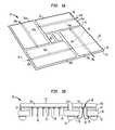
- FIG. 1Ais a diagrammatic perspective view of a microelectronic package according to an embodiment of the present invention.
- FIG. 1Bis a side sectional view of the microelectronic package of FIG. 1A , taken along the line 1 B- 1 B of FIG. 1A .
- FIG. 1Cis a bottom view of the microelectronic package of FIG. 1A , showing the location of the microelectronic elements.
- FIG. 2Ais a diagrammatic perspective view of a microelectronic package according to another embodiment having microelectronic elements flip-chip mounted to a substrate.
- FIG. 2Bis a side sectional view of the microelectronic package of FIG. 2A , taken along the line 2 B- 2 B of FIG. 2A .
- FIGS. 2C and 2Dare side sectional views of variations of the microelectronic package of FIG. 2A , having one or more upper microelectronic elements at least partially overlying corresponding lower microelectronic elements.
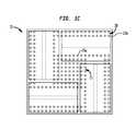
- FIGS. 3A-3Dare top views of microelectronic packages having four microelectronic elements according to further embodiments, showing the location of the bond windows and the central region.
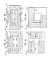
- FIGS. 4A and 4Bare top views of microelectronic packages having three microelectronic elements according to still further embodiments, showing the location of the bond windows and the central region.
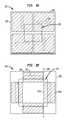
- FIG. 5Ais a diagrammatic perspective view of a microelectronic package according to yet another embodiment having stacked microelectronic elements.
- FIG. 5Bis a side sectional view of the microelectronic package of FIG. 5A , taken along the line 5 B- 5 B of FIG. 5A .
- FIG. 5Cis a bottom view of the microelectronic package of FIG. 5A , showing the location of the microelectronic elements.
- FIG. 6Ais a diagrammatic perspective view of a microelectronic package according to yet another embodiment having stacked microelectronic elements.
- FIG. 6Bis a side sectional view of the microelectronic package of FIG. 6A , taken along the line 6 B- 6 B of FIG. 6A .
- FIG. 6Cis a bottom view of the microelectronic package of FIG. 6A , showing the location of the microelectronic elements.
- FIG. 7is a diagrammatic perspective view of a microelectronic package according to still another embodiment having stacked microelectronic elements.
- FIG. 8Ais a diagrammatic perspective view of a microelectronic assembly having a plurality microelectronic packages mounted to a circuit panel.
- FIG. 8Bis a bottom view of the microelectronic assembly of FIG. 8A .
- FIG. 8C-8Eare diagrammatic perspective views of microelectronic assemblies according to further embodiments having a plurality microelectronic packages mounted to a circuit panel.
- FIG. 9is a schematic depiction of a system according to one embodiment including a plurality of modules.
- Certain embodiments of the inventionprovide a package or microelectronic assembly in which a microelectronic element, e.g., a semiconductor chip, or stacked arrangement of semiconductor chips, is configured to predominantly provide a memory storage array function.
- a microelectronic elemente.g., a semiconductor chip, or stacked arrangement of semiconductor chips
- the number of active devices, e.g., transistors, therein that are configured, i.e., constructed and interconnected with other devices, to provide memory storage array functionis greater than the number of active devices that are configured to provide any other function.
- a microelectronic elementsuch as a DRAM chip may have memory storage array function as its primary or sole function.
- such microelectronic elementmay have mixed use and may incorporate active devices configured to provide memory storage array function, and may also incorporate other active devices configured to provide another function such as processor function, or signal processor or graphics processor function, among others.
- the microelectronic elementmay still have a greater number of active devices configured to provide the memory storage array function than any other function of the microelectronic element.
- Embodiments of the invention hereinprovide packages that have more than one semiconductor chip, i.e., a microelectronic element therein.
- a multiple chip packagecan reduce the amount of area or space required to connect the chips therein to a circuit panel, e.g., printed wiring board to which the package may be electrically and mechanically connected through an array of terminals, such as a ball grid array, land grid array or pin grid array, among others.
- Such connection spaceis particularly limited in small or portable computing devices, e.g., handheld devices such as “smartphones” or tablets that typically combine the function of personal computers with wireless connectivity to the broader world.
- Multi-chip packagescan be particularly useful for making large amounts of relatively inexpensive memory available to a system, such as advanced high performance dynamic random access memory (“DRAM”) chips, e.g., in DDR3 type DRAM chips and its follow-ons.
- DRAMadvanced high performance dynamic random access memory
- the amount of area of the circuit panel needed to connect the multi-chip package theretocan be reduced by providing common terminals on the package through which at least some signals travel on their way to or from two or more chips within the package.
- the traces, vias, and other conductors on a circuit panel that electrically connect the terminals at the exterior of the package with the global wiring on the circuit panelmust not be too long.
- Heat dissipationalso presents a challenge for advanced chips, such that it is desirable for at least one of the large flat surfaces of each chip to be coupled to a heat spreader or be exposed to or in thermal communication with a flow or air within an installed system.
- the packages described belowcan help to further these goals.
- FIGS. 1A-1Cillustrate a particular type of microelectronic package 10 according to an embodiment of the invention.
- the microelectronic package 10can include packaging structure, for example, a substrate 20 having first and second opposed surfaces 21 and 22 .
- the substrate 20can consist essentially of a material having a low coefficient of thermal expansion (“CTE”) in a plane of the substrate (in a direction parallel to the first surface 21 of the substrate), i.e., a CTE of less than 12 parts per million per degree Celsius (hereinafter, “ppm/° C.”), such as a semiconductor material e.g., silicon, or a dielectric material such as ceramic material or silicon dioxide, e.g., glass.
- CTEcoefficient of thermal expansion
- the substrate 20may include a sheet-like substrate that can consist essentially of a polymeric material such as polyimide, epoxy, thermoplastic, thermoset plastic, or other suitable polymeric material or that includes or consists essentially of composite polymeric-inorganic material such as a glass reinforced structure of BT resin (bismaleimide triazine) or epoxy-glass, such as FR-4, among others.
- a substrate 20can consist essentially of a material having a CTE of less than 30 ppm/° C. in the plane of the substrate, i.e., in a direction along its surface.
- the directions parallel to the first surface 21 of the substrate 20are referred to herein as “horizontal” or “lateral” directions, whereas the directions perpendicular to the first surface are referred to herein as upward or downward directions and are also referred to herein as the “vertical” directions.
- the directions referred to hereinare in the frame of reference of the structures referred to. Thus, these directions may lie at any orientation to the normal “up” or “down” directions in a gravitational frame of reference.
- a statement that one feature is disposed at a greater height “above a surface” than another featuremeans that the one feature is at a greater distance in the same orthogonal direction away from the surface than the other feature. Conversely, a statement that one feature is disposed at a lesser height “above a surface” than another feature means that the one feature is at a smaller distance in the same orthogonal direction away from the surface than the other feature.
- At least one aperture 26can extend between the first and second surfaces 21 , 22 of the substrate 20 .
- the substrate 20can have four apertures 26 extending therethrough.
- the substrate 20can have a plurality of terminals 25 , e.g., conductive pads, lands, or conductive posts or pins thereon. Such terminals 25 can be exposed at the second surface of the substrate 20 .
- the terminals 25can function as endpoints for the connection of the microelectronic package 10 with corresponding electrically conductive elements of an external component such as a circuit panel, e.g., printed wiring board, flexible circuit panel, socket, other microelectronic assembly or package, interposer, or passive component assembly, among others (e.g., the circuit panel shown in FIG. 8A ).
- a circuit panele.g., printed wiring board, flexible circuit panel, socket, other microelectronic assembly or package, interposer, or passive component assembly, among others (e.g., the circuit panel shown in FIG. 8A ).
- a circuit panelcan be a motherboard or DIMM module board.
- the terminalscan be arranged in an area array such as a ball-grid array (BGA) (including joining elements as described below), a land-grid array (LGA), or a pin-grid array (PGA), among others.
- the terminals 25can be arranged along the periphery of the second surface 22 of the
- the terminals 25can include substantially rigid posts made from an electrically conductive material such as copper, copper alloy, gold, nickel, and the like.
- the terminals 25can be formed, for example, by plating an electrically conductive material into openings in a resist mask, or by forming posts made, for example, of copper, copper alloy, nickel, or combinations thereof. Such posts can be formed, for example, by subtractively patterning a metal sheet or other metal structure into posts what extend away from the substrate 20 as terminals for electrically interconnecting the microelectronic package 10 with an external component such as the circuit panel 860 described below, for example.
- the terminals 25can be substantially rigid posts having other configurations, as described for example in U.S. Pat. No. 6,177,636, the disclosure of which is hereby incorporated herein by reference. In one example, the terminals 25 can have exposed contact surfaces that are coplanar with one another.
- the microelectronic package 10can include joining elements 11 attached to the terminals 25 for connection with an external component.
- the joining elements 11can be, for example, masses of a bond metal such as solder, tin, indium, a eutectic composition or combination thereof, or another joining material such as a conductive paste or a conductive adhesive.
- the joints between the terminals 25 and contacts of an external componente.g., the circuit panel 860 shown in FIG. 8A
- the joints between the terminals 25 and contacts of an external componentcan include an electrically conductive matrix material such as described in commonly owned U.S. patent application Ser. Nos. 13/155,719 and 13/158,797, the disclosures of which are hereby incorporated by reference herein.
- the jointscan have a similar structure or be formed in a manner as described therein.
- an electrically conductive elementis “exposed at” a surface of a structure indicates that the electrically conductive element is available for contact with a theoretical point moving in a direction perpendicular to the surface toward the surface from outside the structure.
- a terminal or other conductive element which is exposed at a surface of a structurecan project from such surface; can be flush with such surface; or can be recessed relative to such surface and exposed through a hole or depression in the structure.
- the terminals 25can include first terminals 25 a exposed in a central region 23 of the second surface 22 of the substrate 20 and second terminals 25 b exposed in a peripheral region 28 of the second surface outside the central region.
- the arrangement shown in FIGS. 1A-1Ccan provide a compact arrangement of microelectronic elements 30 and a relatively expansive central region 23 without requiring a microelectronic element to overlie any other microelectronic element.
- the first terminals 25 acan be configured to carry all of the command signals, address signals, bank address signals, and clock signals transferred to the microelectronic package 10 from an external component.
- the command signalsare write enable, row address strobe, and column address strobe signals used by a microelectronic element within the microelectronic package 10 , when such microelectronic element is a dynamic random access memory storage device.
- Other signalssuch as ODT (one die termination), chip select, clock enable, are not part of the command signals that need to be carried by the first terminals 25 a.
- the clock signalscan be sampling clocks used for sampling the address signals.
- At least some of the second terminals 25 bcan be configured to carry signals other than the command signals, address signals, and clock signals that are carried by the first terminals 25 a .
- Signals or reference potentialssuch as chip select, reset, power supply voltages, e.g., Vdd, Vddq, and ground, e.g., Vss and Vssq, can be carried by the second terminals 25 b ; none of these signals or reference potentials needs to be carried by the first terminals 25 a.
- the second terminals 25 bcan be disposed in at least one column in each peripheral region 28 .
- at least some of the second terminals 25 b that are configured to carry signals other than the command signals, address signals, and clock signalscan be exposed in the central region 23 of the second surface 22 of the substrate 20 .
- the microelectronic package 10can also include a plurality of microelectronic elements 30 each having a front surface 31 facing the first surface 21 of the substrate 20 .
- each of the microelectronic elements 30can be bare chips or microelectronic units each incorporating a memory storage element such as a dynamic random access memory (“DRAM”) storage array or that is configured to predominantly function as a DRAM storage array (e.g., a DRAM integrated circuit chip).
- a “memory storage element”refers to a multiplicity of memory cells arranged in an array, together with circuitry usable to store and retrieve data therefrom, such as for transport of the data over an electrical interface.
- the microelectronic package 10can be included in a single in-line memory module (“SIMM”) or a dual in-line memory module (“DIMM”).
- a microelectronic element 30 that includes a memory storage elementcan have at least a memory storage array function, but the microelectronic element may not be a full-function memory chip.
- a microelectronic elementmay not have a buffering function itself, but it may be electrically connected to other microelectronic elements in a stack of microelectronic elements, wherein at least one microelectronic element in the stack has a buffering function (the buffering microelectronic element could be a buffer chip, a full-function memory chip, or a controller chip).
- one or more of the microelectronic elements in any of the packages described hereincan embody a greater number of active devices to provide memory storage array function than any other function, e.g., as flash memory, DRAM or other type of memory, and can be arranged in a package together with another microelectronic element or “logic chip” that is configured to predominantly provide logic function.
- the logic chipcan be a programmable or processor element such as a microprocessor or other general purpose computing element.
- the logic chipcan be a microcontroller element, graphics processor, floating point processor, co-processor, digital signal processor, etc.
- the logic chipcan predominantly perform hardware state machine functions, or otherwise be hard-coded to serve a particular function or purpose.
- the logic chipcan be an application specific integrated circuit (“ASIC”) or field programmable gate array (“FPGA”) chip.
- ASICapplication specific integrated circuit
- FPGAfield programmable gate array
- the packagethen may be a “system in a package” (“SIP”).
- SIPsystem in
- a microelectronic element in any of the packages described hereincan have both logic and memory function embedded therein, such as a programmable processor having one or more associated memory storage arrays embedded therewith in the same microelectronic element.
- a microelectronic elementis sometimes referred to as a “system-on-a-chip” (“SOC”), in that logic such as a processor is embedded together with other circuitry such as a memory storage array or circuitry for performing some other function that may be a specialized function.
- SOCsystem-on-a-chip
- each of the microelectronic elements 30can be functionally and mechanically equivalent to the other ones of the microelectronic elements, such that each microelectronic element can have the same pattern of electrically conductive contacts 35 at the front surface 31 with the same function, although the particular dimensions of the length, width, and height of each microelectronic element can be different than that of the other microelectronic elements.
- Each microelectronic element 30can have a plurality of electrically conductive contacts 35 exposed at the front surface 31 thereof.
- the contacts 35 of each microelectronic element 30can be arranged in one or more columns disposed in a central region 36 of the front surface 31 that occupies a central portion of an area of the front surface.
- the central region 36may occupy an area of the front surface 31 that includes a middle third of the shortest distance between opposed peripheral edges 32 a , 32 b of the microelectronic element 30 .
- the contacts 35 of each microelectronic element 30can be aligned with at least one of the apertures 26 .
- the microelectronic package 10can have four microelectronic elements 30 , the contacts 35 of each microelectronic element including eight data I/O contacts. In another embodiment, the microelectronic package 10 can have four microelectronic elements 30 , the contacts 35 of each microelectronic element including sixteen data I/O contacts. In a particular example, the microelectronic package 10 (and any of the other microelectronic packages described herein) can be configured to transfer, i.e., receive by the package, or transmit from the package thirty-two data bits in parallel in a clock cycle.
- the microelectronic package 10(and any of the other microelectronic packages described herein) can be configured to transfer sixty-four data bits in parallel in a clock cycle.
- a number of other data transfer quantitiesare possible, among which only a few such transfer quantities will be mentioned without limitation.
- the microelectronic package 10(and any of the other microelectronic packages described herein) can be configured to transfer seventy-two data bits per clock cycle that can include a set of sixty-four underlying bits that represent data and eight bits that are error correction code (“ECC”) bits for the sixty-four underlying bits.
- ECCerror correction code
- Ninety-six data bits, 108 bits (data and ECC bits), 128 data bits, and 144 bits (data and ECC bits)are other examples of data transfer widths per cycle that the microelectronic package 10 (and any of the other microelectronic packages described herein) can be configured to support.
- At least some signals that pass through the first terminals 25 a of the packagecan be common to at least two of the microelectronic elements 30 . These signals can be routed through connections such as conductive traces extending in a direction parallel to the second surface 22 of the substrate 20 from the first terminals 25 a to the corresponding contacts 35 of the microelectronic elements 30 .
- the microelectronic package 10can route a signal that is common to multiple microelectronic elements 30 through a common first terminal 25 a of the package, rather than through two or more terminals of the package each dedicated to a specific one of the microelectronic elements. In this way, an amount of area of the substrate 20 occupied by such terminals 25 can be reduced.
- FIG. 1Aillustrates a particular arrangement of microelectronic elements 30 a , 30 b , 30 c , and 30 d on a substrate 20 similar to the shape of a pinwheel.
- at least some of the plurality of contacts 35 of each microelectronic element 30can be arranged in a respective column of contacts defining respective first, second, third, and fourth axis 29 a , 29 b , 29 c , and 29 d (collectively axes 29 ).
- first, second, third, and fourth axis 29 a , 29 b , 29 c , and 29 dcollectively axes 29 .
- the first and third axes 29 a and 29 ccan be parallel to one another, the second and fourth axes 29 b and 29 d can be parallel to one another, and the first and third axes can be transverse to the second and fourth axes.
- the first and third axes 29 a and 29 ccan be orthogonal to the second and fourth axes 29 b and 29 d .
- each of the first, second, third and fourth axes 29 a , 29 b , 29 c , and 29 dcan be defined by a length of a corresponding one of the apertures 26 a , 26 b , 26 c , and 26 d , so that the apertures 26 can be arranged in a pinwheel configuration as described above.
- the axis 29 of each microelectronic element 30can bisect the respective microelectronic element and can intersect the area of exactly one other microelectronic element in the microelectronic package 10 .
- the first axis 29 acan bisect the first microelectronic element 30 a and can intersect the area of exactly one other microelectronic element 30 .
- the second axis 29 bcan bisect the second microelectronic element 30 b and can intersect the area of exactly one other microelectronic element 30 .
- the third axis 29 cwhich can bisect the third microelectronic element 30 c and can intersect the area of exactly one other microelectronic element 30 .
- the fourth axis 29 dthat can bisect the fourth microelectronic element 30 d and can intersect the area of exactly one other microelectronic element 30 .
- Electrical connections between the contacts 35 and the terminals 25can include optional leads, e.g., wire bonds 40 , or other possible structure in which at least portions of the leads are aligned with at least one of the apertures 26 .
- at least some of the electrical connectionscan include a wire bond 40 that extends beyond an edge of an aperture 26 in the substrate, and is joined to the contact 35 and a conductive element 24 of the substrate.
- at least some of the electrical connectionscan include lead bonds.
- Such connectionscan include leads that extend along either or both of the first and second surfaces 21 , 22 of the substrate 20 between the conductive elements 24 and the terminals 25 .
- such leadscan be electrically connected between the contacts 35 of each microelectronic element 30 and the terminals 25 , each lead having a portion aligned with at least one of the apertures 26 .
- one or more additional chips 30 ′can be mounted to the substrate 20 having a surface 31 ′ facing the first surface 21 ( FIG. 1A ) or the second surface 22 of the substrate 20 .
- Such an additional chip 30 ′can be flip-chip bonded to electrically conductive contacts exposed at the first surface 21 of the substrate 20 .
- One or more of the additional chips 30 ′can be a buffering chip that can be configured to help provide signal isolation for each of the microelectronic elements 30 with respect to components external to the microelectronic package 10 .
- a buffering chip or buffer elementcan be electrically connected to at least some of the terminals 25 and one or more of the microelectronic elements 30 in the microelectronic package 10 , the buffer element configured to regenerate at least one signal received at one or more of the terminals of the microelectronic package 10 .
- the at least one signalcan include all of the command signals, address signals, bank address signals, and clock signals transferred to the package, the command signals being write enable, row address strobe, and column address strobe signals, and the clock signals being sampling clocks used for sampling the address signals.
- the at least one signalcan include all of the data signals received by the microelectronic package.
- one or more of the additional chips 30 ′can be a decoupling capacitor.
- One or more decoupling capacitorscan be disposed between the microelectronic elements 30 instead of or in addition to the aforementioned buffering chips. Such decoupling capacitors can be electrically connected to internal power and ground buses inside the microelectronic package 10 .
- one of the additional chips 30 ′can be a nonvolatile memory element such as an electrical erasable programmable read only memory (“EEPROM”) mounted to the substrate 20 and configured to permanently store identifying information of the microelectronic package 10 , such as the data width and depth of the microelectronic package.
- EEPROMelectrical erasable programmable read only memory
- Such a nonvolatile memory elementcan be electrically connected to one or more of the microelectronic elements 30 .
- one of the additional chips 30 ′can be a temperature sensor. Such a temperature sensor can be electrically connected to one or more of the microelectronic elements 30 .
- the temperature sensorcan include a diode and can be mounted to the substrate 20 .
- one of the additional chips 30 ′can be a serial presence detect element mounted to the substrate 20 .
- the microelectronic package 10can further include an adhesive 12 between the front surface 31 of the microelectronic elements 30 and the first surface 21 of the substrate 20 .
- the microelectronic package 10can also include an encapsulant (not shown) that can optionally cover, partially cover, or leave uncovered the rear surfaces 32 of the microelectronic elements 30 .
- an encapsulantcan be flowed, stenciled, screened or dispensed onto the rear surfaces 32 of the microelectronic elements 30 .
- the encapsulantcan be a mold compound which is formed thereon by overmolding.
- the contacts of microelectronic elementsmay not be disposed in central regions of the surfaces thereof. Rather, the contacts may be disposed in one or more rows adjacent an edge of such microelectronic element.
- the contacts of a microelectronic elementcan be disposed adjacent two opposed edges of such microelectronic element.
- the contacts of a microelectronic elementcan be disposed adjacent any two edges, or be disposed adjacent more than two edges of such microelectronic element. In such cases, locations of apertures in the substrate can be modified to correspond to such locations of the contacts disposed adjacent such edge or edges of the microelectronic element.
- FIGS. 2A and 2Billustrate a variation of the embodiment described above relative to FIGS. 1A-1C , in which the microelectronic elements 230 are flip-chip bonded to the first surface 221 of the substrate 220 .
- electrical connections between the microelectronic elements 230 and the substrate 220include flip-chip connections extending between contacts of each of the microelectronic elements and conductive bond pads exposed at the first surface 221 of the substrate.
- FIG. 2Cshows a variation of the embodiment described above relative to FIGS. 2A and 2B , in which one or more of the microelectronic elements 230 is a lower microelectronic element 230 ′, and the microelectronic package 210 ′ includes upper microelectronic elements 230 a , 230 b , and 230 c each having a surface at least partially overlying a rear surface 232 of the lower microelectronic element.
- the upper microelectronic elements 230 a , 230 b , and 230 care electrically connected with the lower microelectronic element 230 ′ through at least one conductive via 209 extending through the lower microelectronic element.
- the lower microelectronic element 230 ′′can be wire-bonded to conductive contacts exposed at the second surface 222 of the substrate 220 .
- FIG. 2Dshows a variation of the embodiment described above relative to FIGS. 2A and 2B , in which one or more of the microelectronic elements 230 is a lower microelectronic element 230 ′′, and the microelectronic package 210 ′′ includes upper microelectronic elements 230 a and 230 b each having a surface at least partially overlying a rear surface 232 of the lower microelectronic element. As shown in FIG.
- the upper microelectronic elements 230 a and 230 bare electrically connected with the lower microelectronic element 230 ′′ through wire bonds 240 extending between contacts 235 of the upper microelectronic elements and conductive elements 245 exposed at the rear surface 232 of the lower microelectronic element 230 ′′.
- the lower microelectronic element 230 ′′can be wire-bonded to conductive contacts exposed at the second surface 222 of the substrate 220 .
- FIGS. 3A-3Dshow additional variations of the microelectronic package 10 shown in FIGS. 1A-1C having different locations of the microelectronic elements relative to the first surface of the substrate.
- the respective microelectronic packages 301 , 302 , 303 , and 304can each include four microelectronic elements 330 , each microelectronic element having contacts that are wire-bonded through a respective aperture 326 to conductive contacts exposed at the second surface of the substrate 320 .
- the apertures 326can define portions of the boundary of a central region 323 of the second surface of the substrate, where shared first terminals connected to at least two of the microelectronic elements 330 can be located.
- the microelectronic package 301has microelectronic elements 330 arranged similarly to the microelectronic elements 30 of FIGS. 1A-1C , but the microelectronic elements 330 each have a substantially square shape, so there is very little space at the first surface of the substrate 320 located between the microelectronic elements.
- each of the microelectronic elements 330has first and opposed edges 332 a and 332 b oriented parallel to a length of the respective aperture 326 .
- the first edge 332 a of each of the microelectronic elements 330can define an axis 329 that does not extend through the areas of any of the other microelectronic elements.
- there is a larger space at the first surface of the substrate 320 located between the microelectronic elements 330and the central region 323 of the second surface of the substrate can be relatively large.
- each of the microelectronic elements 330can overlie a respective aperture 326 that defines an axis 329 that does not extend through the areas of any of the other microelectronic elements.
- two of the microelectronic elements 330 a and 330 chave been moved closer to a center of the first surface of the substrate 320 .
- Each of the microelectronic elements 330has first and opposed edges 332 a and 332 b oriented parallel to a length of the respective aperture 326 .
- the first edge 332 a of the first and third microelectronic elements 330 a and 330 ccan define respective axes 329 a and 329 c that extend through the areas of the second and fourth microelectronic elements 330 b and 330 d.
- FIG. 3Dis a variation of FIG. 3C where two of the microelectronic elements 330 a and 330 c have been moved even closer to a center of the first surface of the substrate 320 .
- the first and third microelectronic elements 330 a and 330 bcan overlie a respective aperture 326 a and 326 c that defines a respective axis 329 and 329 ′ that extends through the areas of the second and fourth microelectronic elements 330 b and 330 d .
- each of the microelectronic elements 330has first and opposed edges 332 a and 332 b oriented parallel to a length of the respective aperture 326 .
- the first edge 332 a of the first and third microelectronic elements 330 a and 330 ccan define respective axes 329 a and 329 c that also extend through the areas of the second and fourth microelectronic elements 330 b and 330 d.
- FIGS. 4A and 4Bshow additional variations of the microelectronic package 10 shown in FIGS. 1A-1C having three microelectronic elements having front surfaces arranged in a single plane parallel to the first surface of the substrate 420 .
- the microelectronic package 401has three microelectronic elements 430 mounted to the first side of the substrate 410 .
- a first one of the microelectronic elements 430 acan have additional microelectronic elements at least partially overlying and electrically connected with the first microelectronic element, for example, in a manner such as that shown in FIG. 2C or FIG. 2D .
- a second one of the microelectronic elements 430 bcan be a controller, for example.
- the microelectronic package 402is the same as the microelectronic package 10 shown in FIGS. 1A-1C , except that one of the microelectronic elements 430 in the pinwheel configuration is omitted, leaving three microelectronic elements having front surfaces arranged in a single plane parallel to the first surface of the substrate 420 .
- FIGS. 5A-5Cillustrate a variation of the embodiment described above relative to FIGS. 1A-1C .
- the microelectronic package 510is similar to the microelectronic package 10 shown in FIGS. 1A-1C , except that in the microelectronic package 510 , the front surface 531 of an upper microelectronic element 530 b at least partially overlies a rear surface 532 of each of the four lower microelectronic elements 530 a .
- the lower microelectronic elements 530 a and the upper microelectronic elements 530 bcan be arranged in pairs 507 of microelectronic elements.
- Adjacent pairs 507 of microelectronic elementssuch as a first pair 507 a and a second pair 507 b can be fully spaced apart from one another in a horizontal direction H parallel to the first surface 521 of the substrate 520 .
- the microelectronic elements 530 a and 530 bcan together embody a greater number of active devices to provide memory storage array function than any other function.
- the microelectronic package 510can have eight microelectronic elements 530 (including four lower microelectronic elements 530 a and four upper microelectronic elements 530 b ), each microelectronic element including eight data I/O contacts. In another embodiment, the microelectronic package 510 can have eight microelectronic elements 530 (including four lower microelectronic elements 530 a and four upper microelectronic elements 530 b ), each microelectronic element including nine data I/O contacts.
- first and second axes 529 a and 529 a ′can be transverse to one another.
- first and second axes 529 a and 529 a ′can be orthogonal to one another.
- the first and second axes 529 a and 529 a ′can be parallel to one another.
- each pair of microelectronic elements 507can at least partially overlie an outer aperture 526 a extending between the first and second surfaces 521 , 522 of the substrate 520 .
- Each outer aperture 526 acan have a length defining an outer axis 509 a .
- the four outer axes 509 acan be arranged in a pinwheel configuration as described above, wherein the outer axes 509 a can be arranged in two parallel pairs of outer axes, each pair being transverse to the other pair.
- a central region 523 occupying a central portion of the second surface 522 of the substrate 520can be bounded by the four outer axes 509 a , as shown in FIG. 5C .
- At least some of the terminals 525 exposed at in the central region 523 of the second surface 522 of the substrate 520can be first terminals having a function similar to the first terminals 25 a described above.
- each pair of microelectronic elements 507can also at least partially overlie an inner aperture 526 b extending between the first and second surfaces 521 , 522 of the substrate 520 adjacent a corresponding one of the outer apertures 526 a in the same pair of microelectronic elements, as shown in FIG. 5A .
- Each inner aperture 526 bcan have a length defining an axis 509 b that is closer to a centroid 501 of the substrate than the axis 509 a defined by the length of the corresponding one of the outer apertures 526 a.
- each lower microelectronic element 530 aoverlies an outer aperture 526 a
- each upper microelectronic element 530 boverlies an inner aperture 526 b
- each upper microelectronic element 530 bcan overlie an outer aperture 526 a
- each lower microelectronic element 530 acan overlie an inner aperture 526 b .
- one or more of the lower microelectronic elements 530 acan overlie corresponding outer apertures 526 a
- the other lower microelectronic elementscan overlie corresponding inner apertures 526 b
- one or more of the upper microelectronic elements 530 bcan overlie corresponding outer apertures
- the other upper microelectronic elementscan overlie corresponding inner apertures.
- a spacer 514can be positioned between the front surface 531 of the upper microelectronic elements 530 b and a portion of the first surface 521 of the substrate 520 , with or without an adhesive 512 located between the spacer and the first surface of the substrate.
- a spacer 514can be made, for example, from a dielectric material such as silicon dioxide, a semiconductor material such as silicon, or one or more layers of adhesive. If the spacer 514 includes adhesives, the adhesives can connect the upper microelectronic elements 530 b to the substrate 520 .
- the spacer 514can have substantially the same thickness T 1 in a vertical direction V substantially perpendicular to the first surface 521 of the substrate 520 as the thickness T 2 of the lower microelectronic elements 530 a between the front and rear surfaces 531 , 532 thereof.
- the spacer 514when the spacer 514 is made of an adhesive material, the spacer 514 can be used without an adhesive 512 such as the adhesive 12 described above.
- FIGS. 6A-6Cillustrate a variation of the embodiment described above relative to FIGS. 5A-5C .
- the microelectronic package 610is similar to the microelectronic package 510 shown in FIGS. 5A-5C , except that in the microelectronic package 610 , the front surface 631 of an upper microelectronic element 630 b at least partially overlies a rear surface 632 of two lower microelectronic elements 630 a . All of the lower microelectronic elements 630 a can have front surfaces 631 arranged in a single plane parallel to the first surface 621 of the substrate 620 .
- FIG. 7illustrates another variation of the embodiment described above relative to FIGS. 5A-5C .
- the microelectronic package 710is the same as the microelectronic package 510 shown in FIGS. 5A-5C , except microelectronic package 710 includes three pairs 707 of microelectronic elements, each pair having a lower microelectronic element 730 a and an upper microelectronic element 730 b .
- the microelectronic package 710includes a grouping of two lower microelectronic elements 730 a and one corresponding upper microelectronic element 730 b having a front surface 731 at least partially overlying rear surfaces 732 of each of the upper microelectronic elements.
- the microelectronic package 710can have nine microelectronic elements 730 each including eight data I/O contacts.
- a microelectronic assembly 801can include a plurality of microelectronic packages 810 that can be mounted to a common circuit panel 860 .
- Each of the microelectronic packages 810is shown as a microelectronic package 10 from FIGS. 1A-1C , but such microelectronic packages 810 can be any of the microelectronic packages described above with reference to FIGS. 1A through 7 .
- the circuit panel 860can have first and second opposing surfaces 861 and 862 and pluralities of electrically conductive panel contacts exposed at the respective first and second surfaces.
- the microelectronic packages 810can be mounted to the panel contacts, for example, by the joining elements 11 shown in FIG.
- the circuit panel 860can include an element having a CTE less than 30 ppm/° C. In one embodiment, such an element can consist essentially of semiconductor, glass, ceramic or liquid crystal polymer material.
- the circuit panel 860can have a plurality of parallel exposed edge contacts 850 adjacent an insertion edge 851 of at least one of the first and second surfaces 861 , 862 for mating with corresponding contacts of a socket (shown in FIG. 9 ) when the microelectronic assembly 801 is inserted in the socket. Some or all of the edge contacts 850 can be exposed at either or both of the first or second surfaces 861 , 862 of the microelectronic assembly 801 .
- the circuit panel 860can be a motherboard.
- the circuit panel 860can be a module such as a memory subsystem that can be configured to be attached to another circuit panel such as a motherboard. Such attachment of the circuit panel 860 to another circuit panel can be as described below.
- the exposed edge contacts 850 and the insertion edge 851can be sized for insertion into a corresponding socket ( FIG. 9 ) of other connector of a system, such as can be provided on a motherboard.
- Such exposed edge contacts 850can be suitable for mating with a plurality of corresponding spring contacts ( FIG. 9 ) within such socket connector.
- Such spring contactscan be disposed on single or multiple sides of each slot to mate with corresponding ones of the exposed edge contacts 850 .
- at least some of the edge contacts 850can be usable to carry at least one of a signal or a reference potential between the respective edge contact and one or more of the microelectronic packages 810 .
- the microelectronic assembly 801can have the same signal interface as a dual in-line memory module.
- FIGS. 8C-8Eshow variations of the microelectronic assembly 801 shown in FIGS. 8A and 8B including microelectronic packages 810 ′ that are shown as the microelectronic package 510 from FIGS. 5A-5C .
- the microelectronic package 802has five microelectronic packages 810 ′ mounted to a first side 861 of the circuit panel 860 .
- the microelectronic package 803has five microelectronic packages 810 ′ mounted to a first surface 861 of the circuit panel 860 , and an additional chip 830 ′ such as the additional chip 30 ′ shown in FIG. 1A is shown having a surface facing the first surface of the circuit panel.
- an additional chip 830 ′can be any of the types of additional chips described above with reference to FIGS. 1A-1C , including, for example, a buffering chip that can be configured to help provide signal isolation for each of the microelectronic packages 810 ′ with respect to components external to the microelectronic assembly 803 .
- the additional chip 830 ′can include a memory controller.
- the microelectronic package 804has five microelectronic packages 810 ′ each mounted to a respective socket 805 , and each socket is mounted to the first surface 861 of the circuit panel 860 .
- microelectronic packages and microelectronic assemblies described above with reference to FIGS. 1 through 8Ecan be utilized in construction of diverse electronic systems, such as the system 900 shown in FIG. 9 .
- the system 900 in accordance with a further embodiment of the inventionincludes a plurality of modules or components 906 such as the microelectronic packages and microelectronic assemblies as described above in conjunction with other electronic components 908 and 910 .
- the system 900can include a plurality of sockets 905 , each socket including a plurality of contacts 907 at one or both sides of the socket, such that each socket 905 can be suitable for mating with corresponding exposed edge contacts or exposed module contacts of a corresponding module or component 906 .
- the systemcan include a circuit panel or motherboard 902 such as a flexible printed circuit board, and the circuit panel can include numerous conductors 904 , of which only one is depicted in FIG. 9 , interconnecting the modules or components 906 with one another.
- Such a circuit panel 902can transport signals to and from each of the microelectronic packages 10 or 110 included in the system 900 .
- any suitable structure for making electrical connections between the modules or components 906can be used.
- one or more of the modules or components 906such as the microelectronic package 10 can be mounted directly to the circuit panel 902 .
- the system 900can also include a processor such as the semiconductor chip 908 , such that each module or component 906 can be configured to transfer a number N of data bits in parallel in a clock cycle, and the processor can be configured to transfer a number M of data bits in parallel in a clock cycle, M being greater than or equal to N.
- a processorsuch as the semiconductor chip 908 , such that each module or component 906 can be configured to transfer a number N of data bits in parallel in a clock cycle, and the processor can be configured to transfer a number M of data bits in parallel in a clock cycle, M being greater than or equal to N.
- the system 900can include a processor chip 908 that is configured to transfer thirty-two data bits in parallel in a clock cycle, and the system can also include four modules 906 such as the module 10 described with reference to FIGS. 1A through 1C , each module 906 configured to transfer eight data bits in parallel in a clock cycle (i.e., each module 906 can include first and second microelectronic elements, each of the two microelectronic elements being configured to transfer four data bits in parallel in a clock cycle).
- the system 900can include a processor chip 908 that is configured to transfer sixty-four data bits in parallel in a clock cycle, and the system can also include four modules 906 such as the component 1000 described with reference to FIG. 9 , each module 906 configured to transfer sixteen data bits in parallel in a clock cycle (i.e., each module 906 can include two sets of first and second microelectronic elements, each of the four microelectronic elements being configured to transfer four data bits in parallel in a clock cycle).
- the component 908is a semiconductor chip and component 910 is a display screen, but any other components can be used in the system 900 .
- the system 900can include any number of such components.
- Modules or components 906 and components 908 and 910can be mounted in a common housing 901 , schematically depicted in broken lines, and can be electrically interconnected with one another as necessary to form the desired circuit.
- the housing 901is depicted as a portable housing of the type usable, for example, in a cellular telephone or personal digital assistant, and screen 910 can be exposed at the surface of the housing.
- a structure 906includes a light-sensitive element such as an imaging chip
- a lens 911 or other optical devicealso can be provided for routing light to the structure.
- the simplified system shown in FIG. 9is merely exemplary; other systems, including systems commonly regarded as fixed structures, such as desktop computers, routers and the like can be made using the structures discussed above.
- the rear surface of one or more of the microelectronic elementscan be at least partially exposed at an exterior surface of the microelectronic package after completing fabrication.
- the rear surface 32 of the microelectronic elements 30can be partially or fully exposed at an exterior surface of an encapsulant in the completed microelectronic package 10 .
- the microelectronic packagemay include a heat spreader partly or entirely made of any suitable thermally conductive material.
- suitable thermally conductive materialinclude, but are not limited to, metal, graphite, thermally conductive adhesives, e.g., thermally-conductive epoxy, a solder, or the like, or a combination of such materials.
- the heat spreadercan be a substantially continuous sheet of metal.
- the heat spreadercan include a metallic layer disposed adjacent to one or more of the microelectronic elements.
- the metallic layermay be exposed at the rear surface of the microelectronic element.
- the heat spreadercan include an overmold or an encapsulant covering at least the rear surface of the microelectronic element.
- the heat spreadercan be in thermal communication with at least one of the front surface and rear surface of each of the microelectronic elements such as the lower and/or upper microelectronic elements 530 a , 530 b shown in FIGS. 5A and 5B .
- the heat spreadercan extend between adjacent edges of adjacent ones of the microelectronic elements. The heat spreader can improve heat dissipation to the surrounding environment.
- a pre-formed heat spreader made of metal or other thermally conductive materialmay be attached to or disposed on the rear surface of one or more of the microelectronic elements with a thermally conductive material such as thermally conductive adhesive or thermally conductive grease.
- the adhesiveif present, can be a compliant material that permits relative movement between the heat spreader and the microelectronic element to which it is attached, for example, to accommodate differential thermal expansion between the compliantly attached elements.
- the heat spreadermay be a monolithic structure. Alternatively, the heat spreader may include multiple spreader portions spaced apart from one another.
- the heat spreadermay be or include a layer of solder joined directly to at least a portion of a rear surface of one or more of microelectronic elements such as the lower and/or upper microelectronic elements 530 a , 530 b shown in FIGS. 5A and 5B .
Landscapes
- Engineering & Computer Science (AREA)
- Microelectronics & Electronic Packaging (AREA)
- Power Engineering (AREA)
- Computer Hardware Design (AREA)
- Physics & Mathematics (AREA)
- Condensed Matter Physics & Semiconductors (AREA)
- General Physics & Mathematics (AREA)
- Geometry (AREA)
- Semiconductor Memories (AREA)
- Lead Frames For Integrated Circuits (AREA)
Abstract
Description
Claims (54)
Priority Applications (10)
| Application Number | Priority Date | Filing Date | Title |
|---|---|---|---|
| US13/346,185US8823165B2 (en) | 2011-07-12 | 2012-01-09 | Memory module in a package |
| PCT/US2012/046255WO2013009871A2 (en) | 2011-07-12 | 2012-07-11 | Memory module in a package |
| EP12741161.9AEP2732465A2 (en) | 2011-07-12 | 2012-07-11 | Memory module in a package |
| CN201280044481.5ACN103797578B (en) | 2011-07-12 | 2012-07-11 | Memory Modules in Packages |
| CN201610884451.5ACN107068662A (en) | 2011-07-12 | 2012-07-11 | Memory module in encapsulation |
| JP2014520278AJP2014521223A (en) | 2011-07-12 | 2012-07-11 | Memory module in the package |
| KR1020147003033AKR20140054020A (en) | 2011-07-12 | 2012-07-11 | Memory module in a package |
| TW101125193ATWI532040B (en) | 2011-07-12 | 2012-07-12 | Memory module in a package |
| US14/472,991US9287216B2 (en) | 2011-07-12 | 2014-08-29 | Memory module in a package |
| US15/050,070US9508629B2 (en) | 2011-07-12 | 2016-02-22 | Memory module in a package |
Applications Claiming Priority (5)
| Application Number | Priority Date | Filing Date | Title |
|---|---|---|---|
| US201161506889P | 2011-07-12 | 2011-07-12 | |
| US201161542553P | 2011-10-03 | 2011-10-03 | |
| US201161542488P | 2011-10-03 | 2011-10-03 | |
| US201161542495P | 2011-10-03 | 2011-10-03 | |
| US13/346,185US8823165B2 (en) | 2011-07-12 | 2012-01-09 | Memory module in a package |
Related Child Applications (1)
| Application Number | Title | Priority Date | Filing Date |
|---|---|---|---|
| US14/472,991ContinuationUS9287216B2 (en) | 2011-07-12 | 2014-08-29 | Memory module in a package |
Publications (2)
| Publication Number | Publication Date |
|---|---|
| US20130015590A1 US20130015590A1 (en) | 2013-01-17 |
| US8823165B2true US8823165B2 (en) | 2014-09-02 |
Family
ID=46598952
Family Applications (3)
| Application Number | Title | Priority Date | Filing Date |
|---|---|---|---|
| US13/346,185Active2032-05-31US8823165B2 (en) | 2011-07-12 | 2012-01-09 | Memory module in a package |
| US14/472,991ActiveUS9287216B2 (en) | 2011-07-12 | 2014-08-29 | Memory module in a package |
| US15/050,070ActiveUS9508629B2 (en) | 2011-07-12 | 2016-02-22 | Memory module in a package |
Family Applications After (2)
| Application Number | Title | Priority Date | Filing Date |
|---|---|---|---|
| US14/472,991ActiveUS9287216B2 (en) | 2011-07-12 | 2014-08-29 | Memory module in a package |
| US15/050,070ActiveUS9508629B2 (en) | 2011-07-12 | 2016-02-22 | Memory module in a package |
Country Status (7)
| Country | Link |
|---|---|
| US (3) | US8823165B2 (en) |
| EP (1) | EP2732465A2 (en) |
| JP (1) | JP2014521223A (en) |
| KR (1) | KR20140054020A (en) |
| CN (2) | CN107068662A (en) |
| TW (1) | TWI532040B (en) |
| WO (1) | WO2013009871A2 (en) |
Cited By (16)
| Publication number | Priority date | Publication date | Assignee | Title |
|---|---|---|---|---|
| US20140367866A1 (en)* | 2011-07-12 | 2014-12-18 | Invensas Corporation | Memory module in a package |
| US8981547B2 (en) | 2011-10-03 | 2015-03-17 | Invensas Corporation | Stub minimization for multi-die wirebond assemblies with parallel windows |
| US9070423B2 (en) | 2013-06-11 | 2015-06-30 | Invensas Corporation | Single package dual channel memory with co-support |
| US9224431B2 (en) | 2011-10-03 | 2015-12-29 | Invensas Corporation | Stub minimization using duplicate sets of signal terminals |
| US9281271B2 (en) | 2011-10-03 | 2016-03-08 | Invensas Corporation | Stub minimization using duplicate sets of signal terminals having modulo-x symmetry in assemblies without wirebonds to package substrate |
| US9281296B2 (en) | 2014-07-31 | 2016-03-08 | Invensas Corporation | Die stacking techniques in BGA memory package for small footprint CPU and memory motherboard design |
| US9287195B2 (en) | 2011-10-03 | 2016-03-15 | Invensas Corporation | Stub minimization using duplicate sets of terminals having modulo-x symmetry for wirebond assemblies without windows |
| US9368477B2 (en) | 2012-08-27 | 2016-06-14 | Invensas Corporation | Co-support circuit panel and microelectronic packages |
| US9373565B2 (en) | 2011-10-03 | 2016-06-21 | Invensas Corporation | Stub minimization for assemblies without wirebonds to package substrate |
| US9377824B2 (en) | 2011-10-03 | 2016-06-28 | Invensas Corporation | Microelectronic assembly including memory packages connected to circuit panel, the memory packages having stub minimization for wirebond assemblies without windows |
| US9484080B1 (en) | 2015-11-09 | 2016-11-01 | Invensas Corporation | High-bandwidth memory application with controlled impedance loading |
| US9679613B1 (en) | 2016-05-06 | 2017-06-13 | Invensas Corporation | TFD I/O partition for high-speed, high-density applications |
| US9691437B2 (en) | 2014-09-25 | 2017-06-27 | Invensas Corporation | Compact microelectronic assembly having reduced spacing between controller and memory packages |
| US9859263B2 (en)* | 2015-10-30 | 2018-01-02 | Samsung Electronics Co., Ltd. | Semiconductor package |
| US20200083204A1 (en)* | 2018-09-12 | 2020-03-12 | Toshiba Memory Corporation | Semiconductor memory and manufacturing method thereof |
| US11171114B2 (en)* | 2015-12-02 | 2021-11-09 | Intel Corporation | Die stack with cascade and vertical connections |
Families Citing this family (22)
| Publication number | Priority date | Publication date | Assignee | Title |
|---|---|---|---|---|
| TWI515864B (en) | 2011-10-03 | 2016-01-01 | 英帆薩斯公司 | Stub minimization with terminal grids offset from center of package |
| US10163877B2 (en)* | 2011-11-07 | 2018-12-25 | Taiwan Semiconductor Manufacturing Co., Ltd. | System in package process flow |
| US8848391B2 (en) | 2012-08-27 | 2014-09-30 | Invensas Corporation | Co-support component and microelectronic assembly |
| US8848392B2 (en) | 2012-08-27 | 2014-09-30 | Invensas Corporation | Co-support module and microelectronic assembly |
| US10026714B2 (en)* | 2014-02-14 | 2018-07-17 | Nxp Usa, Inc. | Integrated circuit device |
| US9596331B2 (en) | 2015-01-10 | 2017-03-14 | Seungman Kim | Electronic apparatus having interface to wirelessly communicate with internal wireless device disposed in a housing of the electronic apparatus and a method thereof |
| TWI598721B (en)* | 2015-07-13 | 2017-09-11 | 鴻騰精密科技股份有限公司 | Electrical device |
| US9955605B2 (en)* | 2016-03-30 | 2018-04-24 | Intel Corporation | Hardware interface with space-efficient cell pattern |
| KR102533236B1 (en) | 2016-06-20 | 2023-05-17 | 삼성전자주식회사 | Memory device with improved latency and operating methof thereof |
| JP2018160157A (en)* | 2017-03-23 | 2018-10-11 | 東芝メモリ株式会社 | Semiconductor package |
| US10797020B2 (en)* | 2017-12-29 | 2020-10-06 | Micron Technology, Inc. | Semiconductor device assemblies including multiple stacks of different semiconductor dies |
| US10952327B2 (en)* | 2018-04-27 | 2021-03-16 | Samsung Electronics Co., Ltd. | Semiconductor module |
| EP3837611A4 (en)* | 2018-08-14 | 2022-05-11 | Rambus Inc. | Packaged integrated device |
| US10877908B2 (en) | 2018-09-25 | 2020-12-29 | Micron Technology, Inc. | Isolation component |
| KR102647423B1 (en)* | 2019-03-04 | 2024-03-14 | 에스케이하이닉스 주식회사 | semiconductor package having wire-bonding connection structure and semiconductor package structure including the same |
| TWI703920B (en)* | 2019-05-23 | 2020-09-01 | 十銓科技股份有限公司 | Memory device with lighting function |
| US11610856B2 (en)* | 2019-06-24 | 2023-03-21 | Intel Corporation | Connectivity between integrated circuit dice in a multi-chip package |
| CN110572986B (en)* | 2019-08-27 | 2020-07-21 | 薄林 | A intelligent metering device that radiating efficiency is high for electric power marketing |
| US11621244B2 (en) | 2019-11-15 | 2023-04-04 | Taiwan Semiconductor Manufacturing Company, Ltd. | Integrated circuit package and method |
| US20210263880A1 (en)* | 2020-02-24 | 2021-08-26 | Intel Corporation | Disaggregated die with input/output (i/o) tiles |
| US11705427B2 (en)* | 2021-10-05 | 2023-07-18 | Mellanox Technologies, Ltd. | Mirror-image chips on a common substrate |
| US12255178B2 (en) | 2022-01-26 | 2025-03-18 | Mellanox Technologies, Ltd | Mirror image of geometrical patterns in stacked integrated circuit dies |
Citations (163)
| Publication number | Priority date | Publication date | Assignee | Title |
|---|---|---|---|---|
| US3670208A (en) | 1970-07-13 | 1972-06-13 | Logic Dynamics Inc | Microelectronic package, buss strip and printed circuit base assembly |
| US4747081A (en) | 1983-12-30 | 1988-05-24 | Texas Instruments Incorporated | Video display system using memory with parallel and serial access employing serial shift registers selected by column address |
| US5148266A (en) | 1990-09-24 | 1992-09-15 | Ist Associates, Inc. | Semiconductor chip assemblies having interposer and flexible lead |
| US5148265A (en) | 1990-09-24 | 1992-09-15 | Ist Associates, Inc. | Semiconductor chip assemblies with fan-in leads |
| US5163024A (en) | 1983-12-30 | 1992-11-10 | Texas Instruments Incorporated | Video display system using memory with parallel and serial access employing serial shift registers selected by column address |
| US5210639A (en) | 1983-12-30 | 1993-05-11 | Texas Instruments, Inc. | Dual-port memory with inhibited random access during transfer cycles with serial access |
| US5480840A (en) | 1992-07-14 | 1996-01-02 | At&T Global Information Solutions Company | Multi-chip module with multiple compartments |
| US5679977A (en) | 1990-09-24 | 1997-10-21 | Tessera, Inc. | Semiconductor chip assemblies, methods of making same and components for same |
| US5751553A (en) | 1992-09-16 | 1998-05-12 | Clayton; James E. | Thin multichip module including a connector frame socket having first and second apertures |
| US5777391A (en) | 1994-12-20 | 1998-07-07 | Hitachi, Ltd. | Semiconductor device having an improved connection arrangement between a semiconductor pellet and base substrate electrodes and a method of manufacture thereof |
| US5821614A (en) | 1994-05-06 | 1998-10-13 | Seiko Epson Corporation | Card type semiconductor device |
| US5929517A (en) | 1994-12-29 | 1999-07-27 | Tessera, Inc. | Compliant integrated circuit package and method of fabricating the same |
| US5936305A (en) | 1997-11-20 | 1999-08-10 | Micron Technology, Inc. | Stacked leads-over chip multi-chip module |
| US5973403A (en) | 1996-11-20 | 1999-10-26 | Micron Technology, Inc. | Device and method for stacking wire-bonded integrated circuit dice on flip-chip bonded integrated circuit dice |
| US6086386A (en) | 1996-05-24 | 2000-07-11 | Tessera, Inc. | Flexible connectors for microelectronic elements |
| US6130116A (en) | 1996-12-13 | 2000-10-10 | Tessera, Inc. | Method of encapsulating a microelectronic assembly utilizing a barrier |
| KR20010002214A (en) | 1999-06-12 | 2001-01-05 | 마이클 디. 오브라이언 | A semiconductor packages and manufacturing method for it |
| US6197665B1 (en) | 1998-04-15 | 2001-03-06 | Tessera, Inc. | Lamination machine and method to laminate a coverlay to a microelectronic package |
| US20010002727A1 (en) | 1997-09-16 | 2001-06-07 | Tsukasa Shiraishi | Semiconductor device and module of the same |
| US6252264B1 (en) | 1999-07-30 | 2001-06-26 | International Business Machines Corporation | Integrated circuit chip with features that facilitate a multi-chip module having a number of the chips |
| US6255899B1 (en) | 1999-09-01 | 2001-07-03 | International Business Machines Corporation | Method and apparatus for increasing interchip communications rates |
| US6261867B1 (en) | 1998-03-13 | 2001-07-17 | Stratedge Corporation | Method of making a package for microelectronic devices using iron oxide as a bonding agent |
| US20010022740A1 (en) | 1999-09-02 | 2001-09-20 | Nuxoll James P. | Semiconductor devices having mirrored terminal arrangements, devices including same, and methods of testing such semiconductor devices |
| US6297960B1 (en) | 1998-06-30 | 2001-10-02 | Micron Technology, Inc. | Heat sink with alignment and retaining features |
| US20010038106A1 (en)* | 2000-04-24 | 2001-11-08 | Coteus Paul William | AC drive cross point adjust method and apparatus |
| US6323436B1 (en) | 1997-04-08 | 2001-11-27 | International Business Machines Corporation | High density printed wiring board possessing controlled coefficient of thermal expansion with thin film redistribution layer |
| US20020000583A1 (en) | 1995-11-09 | 2002-01-03 | Goro Kitsukawa | System with meshed power and signal buses on cell array |
| US6343019B1 (en) | 1997-12-22 | 2002-01-29 | Micron Technology, Inc. | Apparatus and method of stacking die on a substrate |
| US20020016056A1 (en)* | 1999-02-19 | 2002-02-07 | Corisis David J. | Methods of packaging an integrated circuit |
| US20020027019A1 (en) | 2000-09-05 | 2002-03-07 | Seiko Epson Corporation | Semiconductor device and method of manufacture thereof, circuit board, and electronic instrument |
| US20020030261A1 (en) | 1999-12-17 | 2002-03-14 | Rolda Ruben A. | Multi-flip-chip semiconductor assembly |
| JP2002076252A (en) | 2000-08-31 | 2002-03-15 | Nec Kyushu Ltd | Semiconductor device |
| US6376769B1 (en) | 1999-05-18 | 2002-04-23 | Amerasia International Technology, Inc. | High-density electronic package, and method for making same |
| US6380318B1 (en) | 1997-07-25 | 2002-04-30 | Nippon Mektron, Limited | Process for producing modified acrylic rubber |
| US6384473B1 (en) | 2000-05-16 | 2002-05-07 | Sandia Corporation | Microelectronic device package with an integral window |
| US20020053732A1 (en) | 1999-05-06 | 2002-05-09 | Hitachi, Ltd. | Semiconductor device |
| EP1205977A2 (en) | 2000-11-07 | 2002-05-15 | Infineon Technologies AG | Memory device with central connecting area |
| US20020066950A1 (en) | 2000-12-04 | 2002-06-06 | Fairchild Semiconductor Corporation | Flip chip in leaded molded package with two dies |
| US6426560B1 (en) | 1999-08-06 | 2002-07-30 | Hitachi, Ltd. | Semiconductor device and memory module |
| US6433422B1 (en) | 1999-05-31 | 2002-08-13 | Mitsubishi Denki Kabushiki Kaisha | Semiconductor integrated circuit having semiconductor packages for mounting integrated circuit chips on both sides of a substrate |
| US6445594B1 (en) | 2000-02-10 | 2002-09-03 | Mitsubishi Denki Kabushiki Kaisha | Semiconductor device having stacked semiconductor elements |
| US6461895B1 (en)* | 1999-01-05 | 2002-10-08 | Intel Corporation | Process for making active interposer for high performance packaging applications |
| US6462423B1 (en) | 2000-08-31 | 2002-10-08 | Micron Technology, Inc. | Flip-chip with matched lines and ground plane |
| US20020171142A1 (en) | 2001-05-21 | 2002-11-21 | Kinsman Larry D. | Bumped die and wire bonded board-on-chip package |
| US20030064547A1 (en) | 1999-02-01 | 2003-04-03 | Salman Akram | High density modularity for IC's |
| US20030089978A1 (en) | 1999-02-26 | 2003-05-15 | Hitachi, Ltd. | Memory-module and a method of manufacturing the same |
| US20030089982A1 (en) | 2001-08-16 | 2003-05-15 | Robert Feurle | Sharing of multiple-access signal line in a printed circuit board |
| US6577004B1 (en) | 2000-08-31 | 2003-06-10 | Micron Technology, Inc. | Solder ball landpad design to improve laminate performance |
| US20030107908A1 (en) | 2001-12-06 | 2003-06-12 | Samsung Electronics Co., Ltd. | Integrated circuit device and module with integrated circuits |
| US6611057B2 (en) | 2000-11-09 | 2003-08-26 | Nec Corporation | Semiconductor device attaining both high speed processing and sufficient cooling capacity |
| US6617695B1 (en) | 2000-05-30 | 2003-09-09 | Mitsubishi Denki Kabushiki Kaisha | Semiconductor device and semiconductor module using the same |
| US6620648B2 (en) | 1999-08-17 | 2003-09-16 | Micron Technology, Inc. | Multi-chip module with extension |
| US6619973B2 (en) | 1995-05-26 | 2003-09-16 | Rambus, Inc. | Chip socket assembly and chip file assembly for semiconductor chips |
| US6633078B2 (en) | 2000-03-21 | 2003-10-14 | Mitsubishi Denki Kabushiki Kaisha | Semiconductor device, method for manufacturing an electronic equipment, electronic equipment and portable information terminal |
| US20030205801A1 (en) | 2002-05-03 | 2003-11-06 | Baik Hyung Gil | Ball grid array package with stacked center pad chips and method for manufacturing the same |
| US20030211660A1 (en) | 2001-12-12 | 2003-11-13 | Micron Technology, Inc. | BOC BGA package for die with I-shaped bond pad layout |
| US6661089B2 (en) | 2000-05-19 | 2003-12-09 | Siliconware Precision Industries Co., Ltd. | Semiconductor package which has no resinous flash formed on lead frame and method for manufacturing the same |
| US20040016999A1 (en) | 2002-07-29 | 2004-01-29 | Mitsubishi Denki Kabushiki Kaisha | Semiconductor device |
| US6692987B2 (en) | 2001-12-12 | 2004-02-17 | Micron Technology, Inc. | BOC BGA package for die with I-shaped bond pad layout |
| US20040061211A1 (en) | 2002-10-01 | 2004-04-01 | Mitsubishi Denki Kabushiki Kaisha | Semiconductor package |
| US20040061577A1 (en) | 2002-02-01 | 2004-04-01 | James Breisch | Dual referenced microstrip |
| US20040090756A1 (en) | 2002-11-07 | 2004-05-13 | Kwun-Yo Ho | Chip packaging structure and manufacturing process thereof |
| US6742098B1 (en) | 2000-10-03 | 2004-05-25 | Intel Corporation | Dual-port buffer-to-memory interface |
| US20040112088A1 (en) | 2000-11-30 | 2004-06-17 | Tetsuji Ueda | Blank for an optical member as well as vessel and method of producing the same |
| US6765288B2 (en) | 2002-08-05 | 2004-07-20 | Tessera, Inc. | Microelectronic adaptors, assemblies and methods |
| US20040145042A1 (en) | 2003-01-14 | 2004-07-29 | Sadayuki Morita | Semiconductor device |
| US6781220B2 (en) | 2001-05-30 | 2004-08-24 | Infineon Technologies Ag | Printed circuit board for semiconductor memory device |
| US20040164382A1 (en) | 2003-02-21 | 2004-08-26 | Gerber Mark A. | Multi-die semiconductor package |
| US20040168826A1 (en) | 2002-03-01 | 2004-09-02 | Tongbi Jiang | Selectively configurable circuit board |
| US20040184240A1 (en) | 2003-03-18 | 2004-09-23 | Ultratera Corporation | Semiconductor package with heat sink |
| US6876088B2 (en) | 2003-01-16 | 2005-04-05 | International Business Machines Corporation | Flex-based IC package construction employing a balanced lamination |
| US6894381B2 (en) | 2002-12-17 | 2005-05-17 | Infineon Technologies Ag | Electronic device having a stack of semiconductor chips and method for the production thereof |
| US20050116358A1 (en) | 2003-11-12 | 2005-06-02 | Tessera,Inc. | Stacked microelectronic assemblies with central contacts |
| US6906415B2 (en) | 2002-06-27 | 2005-06-14 | Micron Technology, Inc. | Semiconductor device assemblies and packages including multiple semiconductor devices and methods |
| US20050194672A1 (en) | 2003-11-04 | 2005-09-08 | Tessera, Inc. | Stacked packages and systems incorporating the same |
| US6943057B1 (en) | 2004-08-31 | 2005-09-13 | Stats Chippac Ltd. | Multichip module package and fabrication method |
| US20050206585A1 (en) | 2000-09-27 | 2005-09-22 | Stewart Roger G | Display devices and integrated circuits |
| US20050243590A1 (en)* | 2003-01-23 | 2005-11-03 | Lee Terry R | Apparatus and methods for optically-coupled memory systems |
| US20050258532A1 (en) | 2004-05-24 | 2005-11-24 | Yasuhiro Yoshikawa | Semiconductor device |
| US6977440B2 (en) | 2001-10-09 | 2005-12-20 | Tessera, Inc. | Stacked packages |
| KR20050119414A (en) | 2004-06-16 | 2005-12-21 | 삼성전자주식회사 | Stacked package comprising two edge pad-type semiconductor chips and method of manufacturing the same |
| US6982485B1 (en) | 2002-02-13 | 2006-01-03 | Amkor Technology, Inc. | Stacking structure for semiconductor chips and a semiconductor package using it |
| US20060004981A1 (en) | 2004-06-30 | 2006-01-05 | Bains Kuljit S | Apparatus and method for initialization of a double-sided dimm having at least one pair of mirrored pins |
| US20060081983A1 (en) | 2004-10-14 | 2006-04-20 | Giles Humpston | Wafer level microelectronic packaging with double isolation |
| US7061105B2 (en) | 2000-01-31 | 2006-06-13 | Hitachi, Ltd. | Semiconductor device and a method of manufacturing the same |
| US7091064B2 (en) | 2002-04-04 | 2006-08-15 | Micron Technology, Inc. | Method and apparatus for attaching microelectronic substrates and support members |
| US20060207788A1 (en) | 2005-03-15 | 2006-09-21 | Chil-Nam Yoon | Memory module and signal line arrangement method thereof |
| US7123497B2 (en) | 2003-04-21 | 2006-10-17 | Elpida Memory, Inc. | Memory module and memory system |
| US7138709B2 (en) | 2003-06-30 | 2006-11-21 | Intel Corporation | Microelectronic package array |
| KR20060120365A (en) | 2005-05-19 | 2006-11-27 | 삼성테크윈 주식회사 | Semiconductor chip stack package |
| US7151319B2 (en) | 2003-06-27 | 2006-12-19 | Hitachi, Ltd. | Semiconductor device |
| US20060290005A1 (en) | 2005-06-28 | 2006-12-28 | Jochen Thomas | Multi-chip device and method for producing a multi-chip device |
| US7170158B2 (en) | 2001-06-29 | 2007-01-30 | Samsung Electronics Co., Ltd. | Double-sided circuit board and multi-chip package including such a circuit board and method for manufacture |
| US20070025131A1 (en) | 2005-07-29 | 2007-02-01 | Hermann Ruckerbauer | Semiconductor memory module and system |
| US20070108592A1 (en) | 2004-12-02 | 2007-05-17 | Siliconware Precision Industries Co., Ltd. | Method for fabricating semiconductor package |
| US20070120245A1 (en) | 2005-11-28 | 2007-05-31 | Yasuhiro Yoshikawa | Semiconductor device |
| US20070143553A1 (en) | 2004-02-05 | 2007-06-21 | Micron Technology, Inc. | Dynamic command and/or address mirroring system and method for memory modules |
| US20070187836A1 (en) | 2006-02-15 | 2007-08-16 | Texas Instruments Incorporated | Package on package design a combination of laminate and tape substrate, with back-to-back die combination |
| US7262507B2 (en) | 2003-12-26 | 2007-08-28 | Nec Electronics Corporation | Semiconductor-mounted device and method for producing same |
| KR20070088177A (en) | 2006-02-24 | 2007-08-29 | 삼성테크윈 주식회사 | Semiconductor package and manufacturing method thereof |
| US7272888B2 (en) | 1996-03-07 | 2007-09-25 | Tessera, Inc. | Method of fabricating semiconductor chip assemblies |
| US20070241441A1 (en) | 2006-04-17 | 2007-10-18 | Stats Chippac Ltd. | Multichip package system |
| US20070260841A1 (en) | 2006-05-02 | 2007-11-08 | Hampel Craig E | Memory module with reduced access granularity |
| US7294928B2 (en) | 2002-09-06 | 2007-11-13 | Tessera, Inc. | Components, methods and assemblies for stacked packages |
| US20080012110A1 (en) | 2006-07-17 | 2008-01-17 | Micron Technology, Inc. | Microelectronic packages with leadframes, including leadframes configured for stacked die packages, and associated systems and methods |
| US7324352B2 (en) | 2004-09-03 | 2008-01-29 | Staktek Group L.P. | High capacity thin module system and method |
| US20080052462A1 (en) | 2006-08-24 | 2008-02-28 | Blakely Robert J | Buffered memory architecture |
| US20080061423A1 (en) | 2006-09-12 | 2008-03-13 | Martin Brox | Method for producing a circuit module comprising at least one integrated circuit |
| US20080088033A1 (en) | 2006-10-17 | 2008-04-17 | Tessera, Inc. | Microelectronic packages and methods therefor |
| US20080098277A1 (en) | 2006-10-23 | 2008-04-24 | International Business Machines Corporation | High density high reliability memory module with power gating and a fault tolerant address and command bus |
| US7368319B2 (en) | 2006-03-17 | 2008-05-06 | Stats Chippac Ltd. | Stacked integrated circuit package-in-package system |
| US7372169B2 (en) | 2005-10-11 | 2008-05-13 | Via Technologies, Inc. | Arrangement of conductive pads on grid array package and on circuit board |
| US7389937B2 (en) | 2004-12-15 | 2008-06-24 | Kabushiki Kaisha Toshiba | Card-shaped memory device incorporating IC card function |
| US20080150155A1 (en) | 2006-12-20 | 2008-06-26 | Shanggar Periaman | Stacked-die packages with silicon vias and surface activated bonding |
| US7405471B2 (en) | 2000-10-16 | 2008-07-29 | Legacy Electronics, Inc. | Carrier-based electronic module |
| US20080182443A1 (en) | 2006-10-12 | 2008-07-31 | International Business Machines Corporation | Socket and Method for Compensating for Differing Coefficients of Thermal Expansion |
| US20080185705A1 (en) | 2005-12-23 | 2008-08-07 | Tessera, Inc. | Microelectronic packages and methods therefor |
| JP3143893U (en) | 2008-02-14 | 2008-08-07 | 華泰電子股▲分▼有限公司 | Multi-chip sealed package |
| US7414312B2 (en) | 2005-05-24 | 2008-08-19 | Kingston Technology Corp. | Memory-module board layout for use with memory chips of different data widths |
| JP2008198841A (en) | 2007-02-14 | 2008-08-28 | Elpida Memory Inc | Semiconductor device |
| US20080230888A1 (en) | 2007-03-19 | 2008-09-25 | Nec Electronics Corporation | Semiconductor device |
| US20080256281A1 (en) | 2007-04-16 | 2008-10-16 | International Business Machines Corporation | System and method for providing an adapter for re-use of legacy dimms in a fully buffered memory environment |
| US20080265397A1 (en) | 2007-04-30 | 2008-10-30 | Chipmos Technology Inc. | Chip-Stacked Package Structure |
| US7476975B2 (en) | 2004-08-23 | 2009-01-13 | Seiko Epson Corporation | Semiconductor device and resin structure therefor |
| KR20090008341A (en) | 2006-05-15 | 2009-01-21 | 산요덴키가부시키가이샤 | Refrigeration unit |
| US20090065948A1 (en) | 2007-09-06 | 2009-03-12 | Micron Technology, Inc. | Package structure for multiple die stack |
| US7518226B2 (en) | 2007-02-06 | 2009-04-14 | Stats Chippac Ltd. | Integrated circuit packaging system with interposer |
| US20090108425A1 (en) | 2007-10-30 | 2009-04-30 | Samsung Electronics Co. Ltd. | Stacked package and method of manufacturing the same |
| US7535110B2 (en) | 2006-06-15 | 2009-05-19 | Marvell World Trade Ltd. | Stack die packages |
| US7550842B2 (en) | 2002-12-12 | 2009-06-23 | Formfactor, Inc. | Integrated circuit assembly |
| KR20090086314A (en) | 2008-02-08 | 2009-08-12 | 가부시끼가이샤 르네사스 테크놀로지 | Semiconductor devices |
| US20090250255A1 (en) | 2008-04-02 | 2009-10-08 | Spansion Llc | Connections for electronic devices on double-sided circuit board |
| US20090250822A1 (en) | 2008-04-07 | 2009-10-08 | Nanya Technology Corporation | Multi-chip stack package |
| US20090294938A1 (en) | 2008-05-27 | 2009-12-03 | Nan-Cheng Chen | Flip-chip package with fan-out wlcsp |
| US7633147B2 (en) | 2002-09-26 | 2009-12-15 | Elpida Memory, Inc. | Semiconductor unit having two device terminals for every one input/output signal |
| US20090314538A1 (en) | 2008-06-20 | 2009-12-24 | Houssam Jomaa | Dual epoxy dielectric and photosensitive solder mask coatings, and processes of making same |
| US7642635B2 (en) | 2003-02-28 | 2010-01-05 | Elpida Memory, Inc. | Stacked semiconductor package |
| US20100052111A1 (en) | 2008-08-26 | 2010-03-04 | Kabushiki Kaisha Toshiba | Stacked-chip device |
| US20100102428A1 (en) | 2008-10-28 | 2010-04-29 | Samsung Electronics Co., Ltd | Semiconductor package |
| JP2010098098A (en) | 2008-10-16 | 2010-04-30 | Denso Corp | Method of manufacturing electronic apparatus |
| US20100182040A1 (en) | 2009-01-22 | 2010-07-22 | International Business Machines Corporation | Programmable through silicon via |
| US7763964B2 (en) | 2007-02-20 | 2010-07-27 | Kabushiki Kaisha Toshiba | Semiconductor device and semiconductor module using the same |
| US7763969B2 (en) | 2005-12-23 | 2010-07-27 | Phoenix Precision Technology Corporation | Structure with semiconductor chips embeded therein |
| US7795721B2 (en) | 2004-06-30 | 2010-09-14 | Nec Electronics Corporation | Semiconductor device and method for manufacturing the same |
| US20100244272A1 (en) | 2008-06-10 | 2010-09-30 | Micron Technology, Inc. | Packaged microelectronic devices and methods for manufacturing packaged microelectronic devices |
| US20100244278A1 (en) | 2009-03-27 | 2010-09-30 | Chipmos Technologies Inc. | Stacked multichip package |
| WO2010120310A1 (en) | 2009-04-17 | 2010-10-21 | Hewlett-Packard Company | Method and system for reducing trace length and capacitance in a large memory footprint background |
| US20100295166A1 (en)* | 2009-05-21 | 2010-11-25 | Samsung Electronics Co., Ltd. | Semiconductor package |
| USRE41972E1 (en) | 1994-07-20 | 2010-11-30 | Sandvik Intellectual Property Ab | Aluminum oxide coated tool |
| US20100301466A1 (en) | 2009-05-29 | 2010-12-02 | Renesas Technology Corp. | Semiconductor device |
| US20100327457A1 (en) | 2008-02-19 | 2010-12-30 | Liquid Design Systems, Inc. | Semiconductor chip and semiconductor device |
| US20110042824A1 (en) | 2009-08-20 | 2011-02-24 | Fujitsu Limited | Multi-chip module and method of manufacturing the same |
| US7989940B2 (en) | 2003-12-19 | 2011-08-02 | Tessera, Inc. | System and method for increasing the number of IO-s on a ball grid package by wire bond stacking of same size packages through apertures |
| US20110193226A1 (en) | 2010-02-08 | 2011-08-11 | Micron Technology, Inc. | Microelectronic devices with through-substrate interconnects and associated methods of manufacturing |
| US20110193178A1 (en) | 2010-02-09 | 2011-08-11 | Taiwan Semiconductor Manufacturing Company, Ltd. | Bottom-Notched SiGe FinFET Formation Using Condensation |
| US20110254156A1 (en) | 2007-12-03 | 2011-10-20 | Stats Chippac, Ltd. | Semiconductor Device and Method of Wafer Level Package Integration |
| US20120020026A1 (en) | 2010-07-23 | 2012-01-26 | Tessera Research Llc | Microelectronic elements with post-assembly planarization |
| US20120018863A1 (en) | 2010-07-23 | 2012-01-26 | Tessera Research Llc | Microelectronic elements with rear contacts connected with via first or via middle structures |
| US8138015B2 (en) | 2008-04-28 | 2012-03-20 | International Business Machines Corporation | Interconnection in multi-chip with interposers and bridges |
| US8345441B1 (en)* | 2011-10-03 | 2013-01-01 | Invensas Corporation | Stub minimization for multi-die wirebond assemblies with parallel windows |
| US8441111B2 (en)* | 2011-10-03 | 2013-05-14 | Invensas Corporation | Stub minimization for multi-die wirebond assemblies with parallel windows |
| US8502390B2 (en) | 2011-07-12 | 2013-08-06 | Tessera, Inc. | De-skewed multi-die packages |
| US8513817B2 (en)* | 2011-07-12 | 2013-08-20 | Invensas Corporation | Memory module in a package |
Family Cites Families (88)
| Publication number | Priority date | Publication date | Assignee | Title |
|---|---|---|---|---|
| JPS5523418Y2 (en) | 1975-01-25 | 1980-06-04 | ||
| JPS641257A (en) | 1987-06-23 | 1989-01-05 | Fujitsu Ltd | Semiconductor device |
| JPH07147386A (en) | 1993-09-29 | 1995-06-06 | Toshiba Micro Electron Kk | Semiconductor device and its manufacturing method and apparatus used for it |
| US6177636B1 (en) | 1994-12-29 | 2001-01-23 | Tessera, Inc. | Connection components with posts |
| TW312044B (en) | 1996-02-23 | 1997-08-01 | Mitsubishi Electric Corp | The semiconductor package |
| JPH09237800A (en) | 1996-02-29 | 1997-09-09 | Toshiba Corp | Semiconductor device |
| US20040061220A1 (en) | 1996-03-22 | 2004-04-01 | Chuichi Miyazaki | Semiconductor device and manufacturing method thereof |
| JP2891665B2 (en) | 1996-03-22 | 1999-05-17 | 株式会社日立製作所 | Semiconductor integrated circuit device and method of manufacturing the same |
| JP3335575B2 (en) | 1997-06-06 | 2002-10-21 | 松下電器産業株式会社 | Semiconductor device and manufacturing method thereof |
| JPH1187640A (en) | 1997-09-09 | 1999-03-30 | Hitachi Ltd | Semiconductor device and electronic device |
| US5949700A (en) | 1998-05-26 | 1999-09-07 | International Business Machines Corporation | Five square vertical dynamic random access memory cell |
| JP3420703B2 (en) | 1998-07-16 | 2003-06-30 | 株式会社東芝 | Method for manufacturing semiconductor device |
| JP3179420B2 (en) | 1998-11-10 | 2001-06-25 | 日本電気株式会社 | Semiconductor device |
| JP3490314B2 (en) | 1998-12-24 | 2004-01-26 | シャープ株式会社 | Multi-chip type semiconductor device |
| US6710446B2 (en) | 1999-12-30 | 2004-03-23 | Renesas Technology Corporation | Semiconductor device comprising stress relaxation layers and method for manufacturing the same |
| JP2002118199A (en) | 2000-10-10 | 2002-04-19 | Mitsubishi Electric Corp | Semiconductor device |
| US6658530B1 (en)* | 2000-10-12 | 2003-12-02 | Sun Microsystems, Inc. | High-performance memory module |
| US6628528B2 (en) | 2000-11-30 | 2003-09-30 | Theodore Zale Schoenborn | Current sharing in memory packages |
| JP5004385B2 (en) | 2001-08-03 | 2012-08-22 | ルネサスエレクトロニクス株式会社 | Semiconductor memory chip and semiconductor memory device using the same |
| WO2003032370A2 (en) | 2001-10-09 | 2003-04-17 | Tessera, Inc. | Stacked packages |
| US6831301B2 (en) | 2001-10-15 | 2004-12-14 | Micron Technology, Inc. | Method and system for electrically coupling a chip to chip package |
| JP2003264256A (en) | 2002-03-08 | 2003-09-19 | Hitachi Ltd | Semiconductor device |
| TW567593B (en) | 2002-03-21 | 2003-12-21 | Nanya Technology Corp | Packaging method of memory and apparatus of the same |
| DE10234951B4 (en) | 2002-07-31 | 2009-01-02 | Qimonda Ag | Process for the production of semiconductor circuit modules |
| JP3742051B2 (en) | 2002-10-31 | 2006-02-01 | エルピーダメモリ株式会社 | Memory module, memory chip, and memory system |
| US7102217B2 (en) | 2003-04-09 | 2006-09-05 | Micron Technology, Inc. | Interposer substrates with reinforced interconnect slots, and semiconductor die packages including same |
| JP3940694B2 (en) | 2003-04-18 | 2007-07-04 | 株式会社東芝 | Semiconductor device and manufacturing method thereof |
| WO2005048307A2 (en) | 2003-11-08 | 2005-05-26 | Chippac, Inc. | Flip chip interconnection pad layout |
| JP4119866B2 (en) | 2004-05-12 | 2008-07-16 | 富士通株式会社 | Semiconductor device |
| JP4543755B2 (en) | 2004-05-31 | 2010-09-15 | パナソニック株式会社 | Semiconductor integrated circuit |
| DE102004049356B4 (en) | 2004-10-08 | 2006-06-29 | Infineon Technologies Ag | Semiconductor module with an internal semiconductor chip stack and method for producing the same |
| US20060087013A1 (en) | 2004-10-21 | 2006-04-27 | Etron Technology, Inc. | Stacked multiple integrated circuit die package assembly |
| JP4674850B2 (en) | 2005-02-25 | 2011-04-20 | ルネサスエレクトロニクス株式会社 | Semiconductor device |
| JP4707446B2 (en)* | 2005-04-26 | 2011-06-22 | 富士通セミコンダクター株式会社 | Semiconductor device |
| CN101278394B (en) | 2005-10-03 | 2010-05-19 | 罗姆股份有限公司 | Semiconductor device |
| JP2007013146A (en) | 2006-06-26 | 2007-01-18 | Renesas Technology Corp | Semiconductor integrated circuit device |
| JP4362784B2 (en) | 2006-07-06 | 2009-11-11 | エルピーダメモリ株式会社 | Semiconductor device |
| JP4791924B2 (en) | 2006-09-22 | 2011-10-12 | 株式会社東芝 | Semiconductor memory device |
| US20080088030A1 (en)* | 2006-10-16 | 2008-04-17 | Formfactor, Inc. | Attaching and interconnecting dies to a substrate |
| JP4389228B2 (en) | 2006-11-29 | 2009-12-24 | エルピーダメモリ株式会社 | Memory module |
| KR101257912B1 (en) | 2007-02-14 | 2013-04-24 | 삼성전자주식회사 | Semiconductor memory device and method of arranging terminals of the same, and memory module comprising the device and method of arranging terminals and lines on board of the same |
| CN101617371B (en) | 2007-02-16 | 2014-03-26 | 莫塞德技术公司 | Non-volatile semiconductor memory with multiple external power supplies |
| TW200842998A (en) | 2007-04-18 | 2008-11-01 | Siliconware Precision Industries Co Ltd | Semiconductor device and manufacturing method thereof |
| TWI335055B (en) | 2007-06-29 | 2010-12-21 | Chipmos Technologies Inc | Chip-stacked package structure |
| US10074553B2 (en) | 2007-12-03 | 2018-09-11 | STATS ChipPAC Pte. Ltd. | Wafer level package integration and method |
| JP5497266B2 (en) | 2008-01-31 | 2014-05-21 | ピーエスフォー ルクスコ エスエイアールエル | Semiconductor module, substrate and wiring method |
| US7855445B2 (en) | 2008-04-29 | 2010-12-21 | Silicon Laboratories, Inc. | Circuit device including rotated stacked die |
| US8264085B2 (en) | 2008-05-05 | 2012-09-11 | Infineon Technologies Ag | Semiconductor device package interconnections |
| CN101604685A (en)* | 2008-06-11 | 2009-12-16 | 英业达股份有限公司 | Memory module |
| KR101479461B1 (en) | 2008-10-14 | 2015-01-06 | 삼성전자주식회사 | Laminated package and method of manufacturing the same |
| TWM363079U (en) | 2009-03-24 | 2009-08-11 | Xintec Inc | Semiconductor device and layout structure for array package |
| US8586870B2 (en) | 2009-03-27 | 2013-11-19 | Molex Incorporated | Microelectronic component support with reinforced structure |
| JP2010282510A (en) | 2009-06-05 | 2010-12-16 | Elpida Memory Inc | Memory module |
| JP5593053B2 (en)* | 2009-10-09 | 2014-09-17 | ピーエスフォー ルクスコ エスエイアールエル | Semiconductor device |
| TWI390645B (en) | 2009-10-22 | 2013-03-21 | Powertech Technology Inc | Back-to-back chip assembly stacked packaging method and structure |
| US8304286B2 (en) | 2009-12-11 | 2012-11-06 | Stats Chippac Ltd. | Integrated circuit packaging system with shielded package and method of manufacture thereof |
| US8508954B2 (en) | 2009-12-17 | 2013-08-13 | Samsung Electronics Co., Ltd. | Systems employing a stacked semiconductor package |
| JP2011155203A (en) | 2010-01-28 | 2011-08-11 | Elpida Memory Inc | Semiconductor device |
| KR101871317B1 (en) | 2010-08-13 | 2018-06-27 | 테사 소시에타스 유로파에아 | Method for encapsulating an electronic arrangement |
| TWI533412B (en) | 2010-08-13 | 2016-05-11 | 金龍國際公司 | Semiconductor device package structure and forming method of the same |
| US8378478B2 (en) | 2010-11-24 | 2013-02-19 | Tessera, Inc. | Enhanced stacked microelectronic assemblies with central contacts and vias connected to the central contacts |
| JP4979097B2 (en) | 2010-12-06 | 2012-07-18 | ルネサスエレクトロニクス株式会社 | Multi-chip module |
| KR101118711B1 (en) | 2010-12-17 | 2012-03-12 | 테세라, 인코포레이티드 | Enhanced stacked microelectric assemblies with central contacts |
| KR101061531B1 (en) | 2010-12-17 | 2011-09-01 | 테세라 리써치 엘엘씨 | Enhanced stacked microelectronic assemblies with central contacts and improved ground or power distribution |
| US9143140B2 (en) | 2011-02-15 | 2015-09-22 | Cavium, Inc. | Multi-function delay locked loop |
| US8466544B2 (en) | 2011-02-25 | 2013-06-18 | Stats Chippac, Ltd. | Semiconductor device and method of forming interposer and opposing build-up interconnect structure with connecting conductive TMV for electrical interconnect of Fo-WLCSP |
| US8338963B2 (en) | 2011-04-21 | 2012-12-25 | Tessera, Inc. | Multiple die face-down stacking for two or more die |
| US8304881B1 (en) | 2011-04-21 | 2012-11-06 | Tessera, Inc. | Flip-chip, face-up and face-down wirebond combination package |
| US8970028B2 (en) | 2011-12-29 | 2015-03-03 | Invensas Corporation | Embedded heat spreader for package with multiple microelectronic elements and face-down connection |
| US8890304B2 (en) | 2011-06-08 | 2014-11-18 | Tessera, Inc. | Fan-out microelectronic unit WLP having interconnects comprising a matrix of a high melting point, a low melting point and a polymer material |
| US9117811B2 (en) | 2011-06-13 | 2015-08-25 | Tessera, Inc. | Flip chip assembly and process with sintering material on metal bumps |
| KR20130005465A (en) | 2011-07-06 | 2013-01-16 | 삼성전자주식회사 | Semiconductor stack package apparatus |
| US8421237B2 (en) | 2011-07-07 | 2013-04-16 | Cisco Technology, Inc. | Stacked memory layers having multiple orientations and through-layer interconnects |
| US8823165B2 (en)* | 2011-07-12 | 2014-09-02 | Invensas Corporation | Memory module in a package |
| US8405207B1 (en) | 2011-10-03 | 2013-03-26 | Invensas Corporation | Stub minimization for wirebond assemblies without windows |
| US8653646B2 (en) | 2011-10-03 | 2014-02-18 | Invensas Corporation | Stub minimization using duplicate sets of terminals for wirebond assemblies without windows |
| TWI515864B (en) | 2011-10-03 | 2016-01-01 | 英帆薩斯公司 | Stub minimization with terminal grids offset from center of package |
| US8525327B2 (en) | 2011-10-03 | 2013-09-03 | Invensas Corporation | Stub minimization for assemblies without wirebonds to package substrate |
| JP5947904B2 (en) | 2011-10-03 | 2016-07-06 | インヴェンサス・コーポレイション | Stub minimization for multi-die wirebond assemblies with orthogonal windows |
| US8436457B2 (en) | 2011-10-03 | 2013-05-07 | Invensas Corporation | Stub minimization for multi-die wirebond assemblies with parallel windows |
| KR101894823B1 (en) | 2011-10-03 | 2018-09-04 | 인벤사스 코포레이션 | Stub minimization for multi-die wirebond assemblies with parallel windows |
| US8436477B2 (en) | 2011-10-03 | 2013-05-07 | Invensas Corporation | Stub minimization using duplicate sets of signal terminals in assemblies without wirebonds to package substrate |
| TWM426922U (en) | 2011-11-08 | 2012-04-11 | Wistron Neweb Corp | Memory card connector |
| US8848391B2 (en) | 2012-08-27 | 2014-09-30 | Invensas Corporation | Co-support component and microelectronic assembly |
| US8787034B2 (en) | 2012-08-27 | 2014-07-22 | Invensas Corporation | Co-support system and microelectronic assembly |
| US8848392B2 (en) | 2012-08-27 | 2014-09-30 | Invensas Corporation | Co-support module and microelectronic assembly |
| US8902680B2 (en) | 2013-01-23 | 2014-12-02 | Micron Technology, Inc. | Identifying stacked dice |
| US9070423B2 (en) | 2013-06-11 | 2015-06-30 | Invensas Corporation | Single package dual channel memory with co-support |
- 2012
- 2012-01-09USUS13/346,185patent/US8823165B2/enactiveActive
- 2012-07-11JPJP2014520278Apatent/JP2014521223A/enactivePending
- 2012-07-11CNCN201610884451.5Apatent/CN107068662A/enactivePending
- 2012-07-11EPEP12741161.9Apatent/EP2732465A2/ennot_activeWithdrawn
- 2012-07-11WOPCT/US2012/046255patent/WO2013009871A2/enactiveApplication Filing
- 2012-07-11CNCN201280044481.5Apatent/CN103797578B/ennot_activeExpired - Fee Related
- 2012-07-11KRKR1020147003033Apatent/KR20140054020A/ennot_activeAbandoned
- 2012-07-12TWTW101125193Apatent/TWI532040B/ennot_activeIP Right Cessation
- 2014
- 2014-08-29USUS14/472,991patent/US9287216B2/enactiveActive
- 2016
- 2016-02-22USUS15/050,070patent/US9508629B2/enactiveActive
Patent Citations (185)
| Publication number | Priority date | Publication date | Assignee | Title |
|---|---|---|---|---|
| US3670208A (en) | 1970-07-13 | 1972-06-13 | Logic Dynamics Inc | Microelectronic package, buss strip and printed circuit base assembly |
| US4747081A (en) | 1983-12-30 | 1988-05-24 | Texas Instruments Incorporated | Video display system using memory with parallel and serial access employing serial shift registers selected by column address |
| US5163024A (en) | 1983-12-30 | 1992-11-10 | Texas Instruments Incorporated | Video display system using memory with parallel and serial access employing serial shift registers selected by column address |
| US5210639A (en) | 1983-12-30 | 1993-05-11 | Texas Instruments, Inc. | Dual-port memory with inhibited random access during transfer cycles with serial access |
| US5148266A (en) | 1990-09-24 | 1992-09-15 | Ist Associates, Inc. | Semiconductor chip assemblies having interposer and flexible lead |
| US5148265A (en) | 1990-09-24 | 1992-09-15 | Ist Associates, Inc. | Semiconductor chip assemblies with fan-in leads |
| US5679977A (en) | 1990-09-24 | 1997-10-21 | Tessera, Inc. | Semiconductor chip assemblies, methods of making same and components for same |
| US5480840A (en) | 1992-07-14 | 1996-01-02 | At&T Global Information Solutions Company | Multi-chip module with multiple compartments |
| US5751553A (en) | 1992-09-16 | 1998-05-12 | Clayton; James E. | Thin multichip module including a connector frame socket having first and second apertures |
| US5821614A (en) | 1994-05-06 | 1998-10-13 | Seiko Epson Corporation | Card type semiconductor device |
| USRE41972E1 (en) | 1994-07-20 | 2010-11-30 | Sandvik Intellectual Property Ab | Aluminum oxide coated tool |
| US5777391A (en) | 1994-12-20 | 1998-07-07 | Hitachi, Ltd. | Semiconductor device having an improved connection arrangement between a semiconductor pellet and base substrate electrodes and a method of manufacture thereof |
| USRE42972E1 (en) | 1994-12-20 | 2011-11-29 | Renesas Electronics Corporation | Semiconductor device having an improved connection arrangement between a semiconductor pellet and base substrate electrodes and a method of manufacture thereof |
| USRE41478E1 (en) | 1994-12-20 | 2010-08-10 | Renesas Electronics Corporation | Semiconductor device having an improved connection arrangement between a semiconductor pellet and base substrate electrodes and a method of manufacture thereof |
| USRE41722E1 (en) | 1994-12-20 | 2010-09-21 | Renesas Electronics Corp. | Semiconductor device having an improved connection arrangement between a semiconductor pellet and base substrate electrodes and a method of manufacture thereof |
| USRE41721E1 (en) | 1994-12-20 | 2010-09-21 | Renesas Electronics Corporation | Semiconductor device having an improved connected arrangement between a semiconductor pellet and base substrate electrodes |
| US5929517A (en) | 1994-12-29 | 1999-07-27 | Tessera, Inc. | Compliant integrated circuit package and method of fabricating the same |
| US6619973B2 (en) | 1995-05-26 | 2003-09-16 | Rambus, Inc. | Chip socket assembly and chip file assembly for semiconductor chips |
| US20020000583A1 (en) | 1995-11-09 | 2002-01-03 | Goro Kitsukawa | System with meshed power and signal buses on cell array |
| US7272888B2 (en) | 1996-03-07 | 2007-09-25 | Tessera, Inc. | Method of fabricating semiconductor chip assemblies |
| US6086386A (en) | 1996-05-24 | 2000-07-11 | Tessera, Inc. | Flexible connectors for microelectronic elements |
| US6707141B2 (en) | 1996-06-26 | 2004-03-16 | Micron Technology, Inc. | Multi-chip module substrate for use with leads-over chip type semiconductor devices |
| US5973403A (en) | 1996-11-20 | 1999-10-26 | Micron Technology, Inc. | Device and method for stacking wire-bonded integrated circuit dice on flip-chip bonded integrated circuit dice |
| US6130116A (en) | 1996-12-13 | 2000-10-10 | Tessera, Inc. | Method of encapsulating a microelectronic assembly utilizing a barrier |
| US6821815B2 (en) | 1996-12-13 | 2004-11-23 | Tessera, Inc. | Method of assembling a semiconductor chip package |
| US6323436B1 (en) | 1997-04-08 | 2001-11-27 | International Business Machines Corporation | High density printed wiring board possessing controlled coefficient of thermal expansion with thin film redistribution layer |
| US6380318B1 (en) | 1997-07-25 | 2002-04-30 | Nippon Mektron, Limited | Process for producing modified acrylic rubber |
| US20010002727A1 (en) | 1997-09-16 | 2001-06-07 | Tsukasa Shiraishi | Semiconductor device and module of the same |
| US5936305A (en) | 1997-11-20 | 1999-08-10 | Micron Technology, Inc. | Stacked leads-over chip multi-chip module |
| US6343019B1 (en) | 1997-12-22 | 2002-01-29 | Micron Technology, Inc. | Apparatus and method of stacking die on a substrate |
| US6261867B1 (en) | 1998-03-13 | 2001-07-17 | Stratedge Corporation | Method of making a package for microelectronic devices using iron oxide as a bonding agent |
| US6197665B1 (en) | 1998-04-15 | 2001-03-06 | Tessera, Inc. | Lamination machine and method to laminate a coverlay to a microelectronic package |
| US6297960B1 (en) | 1998-06-30 | 2001-10-02 | Micron Technology, Inc. | Heat sink with alignment and retaining features |
| US6461895B1 (en)* | 1999-01-05 | 2002-10-08 | Intel Corporation | Process for making active interposer for high performance packaging applications |
| US7061092B2 (en) | 1999-02-01 | 2006-06-13 | Micron Technology, Inc. | High-density modularity for ICS |
| US20030064547A1 (en) | 1999-02-01 | 2003-04-03 | Salman Akram | High density modularity for IC's |
| US20020016056A1 (en)* | 1999-02-19 | 2002-02-07 | Corisis David J. | Methods of packaging an integrated circuit |
| US20030089978A1 (en) | 1999-02-26 | 2003-05-15 | Hitachi, Ltd. | Memory-module and a method of manufacturing the same |
| US20020053732A1 (en) | 1999-05-06 | 2002-05-09 | Hitachi, Ltd. | Semiconductor device |
| US6452266B1 (en) | 1999-05-06 | 2002-09-17 | Hitachi, Ltd. | Semiconductor device |
| US6376769B1 (en) | 1999-05-18 | 2002-04-23 | Amerasia International Technology, Inc. | High-density electronic package, and method for making same |
| US6433422B1 (en) | 1999-05-31 | 2002-08-13 | Mitsubishi Denki Kabushiki Kaisha | Semiconductor integrated circuit having semiconductor packages for mounting integrated circuit chips on both sides of a substrate |
| KR20010002214A (en) | 1999-06-12 | 2001-01-05 | 마이클 디. 오브라이언 | A semiconductor packages and manufacturing method for it |
| US6252264B1 (en) | 1999-07-30 | 2001-06-26 | International Business Machines Corporation | Integrated circuit chip with features that facilitate a multi-chip module having a number of the chips |
| US6426560B1 (en) | 1999-08-06 | 2002-07-30 | Hitachi, Ltd. | Semiconductor device and memory module |
| US6620648B2 (en) | 1999-08-17 | 2003-09-16 | Micron Technology, Inc. | Multi-chip module with extension |
| US6255899B1 (en) | 1999-09-01 | 2001-07-03 | International Business Machines Corporation | Method and apparatus for increasing interchip communications rates |
| US20010022740A1 (en) | 1999-09-02 | 2001-09-20 | Nuxoll James P. | Semiconductor devices having mirrored terminal arrangements, devices including same, and methods of testing such semiconductor devices |
| US20020030261A1 (en) | 1999-12-17 | 2002-03-14 | Rolda Ruben A. | Multi-flip-chip semiconductor assembly |
| US7061105B2 (en) | 2000-01-31 | 2006-06-13 | Hitachi, Ltd. | Semiconductor device and a method of manufacturing the same |
| US7633146B2 (en) | 2000-01-31 | 2009-12-15 | Elpida Memory Inc. | Semiconductor device and a method of manufacturing the same |
| US6445594B1 (en) | 2000-02-10 | 2002-09-03 | Mitsubishi Denki Kabushiki Kaisha | Semiconductor device having stacked semiconductor elements |
| US6633078B2 (en) | 2000-03-21 | 2003-10-14 | Mitsubishi Denki Kabushiki Kaisha | Semiconductor device, method for manufacturing an electronic equipment, electronic equipment and portable information terminal |
| US20010038106A1 (en)* | 2000-04-24 | 2001-11-08 | Coteus Paul William | AC drive cross point adjust method and apparatus |
| US6384473B1 (en) | 2000-05-16 | 2002-05-07 | Sandia Corporation | Microelectronic device package with an integral window |
| US6661089B2 (en) | 2000-05-19 | 2003-12-09 | Siliconware Precision Industries Co., Ltd. | Semiconductor package which has no resinous flash formed on lead frame and method for manufacturing the same |
| US6617695B1 (en) | 2000-05-30 | 2003-09-09 | Mitsubishi Denki Kabushiki Kaisha | Semiconductor device and semiconductor module using the same |
| US20020053727A1 (en) | 2000-08-31 | 2002-05-09 | Naoto Kimura | Semiconductor device |
| US6577004B1 (en) | 2000-08-31 | 2003-06-10 | Micron Technology, Inc. | Solder ball landpad design to improve laminate performance |
| US6462423B1 (en) | 2000-08-31 | 2002-10-08 | Micron Technology, Inc. | Flip-chip with matched lines and ground plane |
| JP2002076252A (en) | 2000-08-31 | 2002-03-15 | Nec Kyushu Ltd | Semiconductor device |
| US20020027019A1 (en) | 2000-09-05 | 2002-03-07 | Seiko Epson Corporation | Semiconductor device and method of manufacture thereof, circuit board, and electronic instrument |
| US20050206585A1 (en) | 2000-09-27 | 2005-09-22 | Stewart Roger G | Display devices and integrated circuits |
| US6742098B1 (en) | 2000-10-03 | 2004-05-25 | Intel Corporation | Dual-port buffer-to-memory interface |
| US7405471B2 (en) | 2000-10-16 | 2008-07-29 | Legacy Electronics, Inc. | Carrier-based electronic module |
| US6560134B2 (en) | 2000-11-07 | 2003-05-06 | Infineon Technologies Ag | Memory configuration with a central connection area |
| EP1205977A2 (en) | 2000-11-07 | 2002-05-15 | Infineon Technologies AG | Memory device with central connecting area |
| US6611057B2 (en) | 2000-11-09 | 2003-08-26 | Nec Corporation | Semiconductor device attaining both high speed processing and sufficient cooling capacity |
| US20040112088A1 (en) | 2000-11-30 | 2004-06-17 | Tetsuji Ueda | Blank for an optical member as well as vessel and method of producing the same |
| US20020066950A1 (en) | 2000-12-04 | 2002-06-06 | Fairchild Semiconductor Corporation | Flip chip in leaded molded package with two dies |
| US20020171142A1 (en) | 2001-05-21 | 2002-11-21 | Kinsman Larry D. | Bumped die and wire bonded board-on-chip package |
| US6744137B2 (en) | 2001-05-21 | 2004-06-01 | Micron Technology, Inc. | Bumped die and wire bonded board-on-chip package |
| US6781220B2 (en) | 2001-05-30 | 2004-08-24 | Infineon Technologies Ag | Printed circuit board for semiconductor memory device |
| US7170158B2 (en) | 2001-06-29 | 2007-01-30 | Samsung Electronics Co., Ltd. | Double-sided circuit board and multi-chip package including such a circuit board and method for manufacture |
| US6894379B2 (en) | 2001-08-16 | 2005-05-17 | Infineon Technologies Ag | Sharing of multiple-access signal line in a printed circuit board |
| US20030089982A1 (en) | 2001-08-16 | 2003-05-15 | Robert Feurle | Sharing of multiple-access signal line in a printed circuit board |
| US6977440B2 (en) | 2001-10-09 | 2005-12-20 | Tessera, Inc. | Stacked packages |
| US20030107908A1 (en) | 2001-12-06 | 2003-06-12 | Samsung Electronics Co., Ltd. | Integrated circuit device and module with integrated circuits |
| US20030211660A1 (en) | 2001-12-12 | 2003-11-13 | Micron Technology, Inc. | BOC BGA package for die with I-shaped bond pad layout |
| US6692987B2 (en) | 2001-12-12 | 2004-02-17 | Micron Technology, Inc. | BOC BGA package for die with I-shaped bond pad layout |
| US6720666B2 (en) | 2001-12-12 | 2004-04-13 | Micron Technology, Inc. | BOC BGA package for die with I-shaped bond pad layout |
| US20040061577A1 (en) | 2002-02-01 | 2004-04-01 | James Breisch | Dual referenced microstrip |
| US6982485B1 (en) | 2002-02-13 | 2006-01-03 | Amkor Technology, Inc. | Stacking structure for semiconductor chips and a semiconductor package using it |
| US20040168826A1 (en) | 2002-03-01 | 2004-09-02 | Tongbi Jiang | Selectively configurable circuit board |
| US7091064B2 (en) | 2002-04-04 | 2006-08-15 | Micron Technology, Inc. | Method and apparatus for attaching microelectronic substrates and support members |
| US20030205801A1 (en) | 2002-05-03 | 2003-11-06 | Baik Hyung Gil | Ball grid array package with stacked center pad chips and method for manufacturing the same |
| US6906415B2 (en) | 2002-06-27 | 2005-06-14 | Micron Technology, Inc. | Semiconductor device assemblies and packages including multiple semiconductor devices and methods |
| US20040016999A1 (en) | 2002-07-29 | 2004-01-29 | Mitsubishi Denki Kabushiki Kaisha | Semiconductor device |
| JP2004063767A (en) | 2002-07-29 | 2004-02-26 | Renesas Technology Corp | Semiconductor device |
| US6765288B2 (en) | 2002-08-05 | 2004-07-20 | Tessera, Inc. | Microelectronic adaptors, assemblies and methods |
| US7294928B2 (en) | 2002-09-06 | 2007-11-13 | Tessera, Inc. | Components, methods and assemblies for stacked packages |
| US7633147B2 (en) | 2002-09-26 | 2009-12-15 | Elpida Memory, Inc. | Semiconductor unit having two device terminals for every one input/output signal |
| US6836007B2 (en) | 2002-10-01 | 2004-12-28 | Renesas Technology Corp. | Semiconductor package including stacked semiconductor chips |
| US20040061211A1 (en) | 2002-10-01 | 2004-04-01 | Mitsubishi Denki Kabushiki Kaisha | Semiconductor package |
| US20040090756A1 (en) | 2002-11-07 | 2004-05-13 | Kwun-Yo Ho | Chip packaging structure and manufacturing process thereof |
| US7550842B2 (en) | 2002-12-12 | 2009-06-23 | Formfactor, Inc. | Integrated circuit assembly |
| US6894381B2 (en) | 2002-12-17 | 2005-05-17 | Infineon Technologies Ag | Electronic device having a stack of semiconductor chips and method for the production thereof |
| US20040145042A1 (en) | 2003-01-14 | 2004-07-29 | Sadayuki Morita | Semiconductor device |
| US6876088B2 (en) | 2003-01-16 | 2005-04-05 | International Business Machines Corporation | Flex-based IC package construction employing a balanced lamination |
| US20050243590A1 (en)* | 2003-01-23 | 2005-11-03 | Lee Terry R | Apparatus and methods for optically-coupled memory systems |
| US20040164382A1 (en) | 2003-02-21 | 2004-08-26 | Gerber Mark A. | Multi-die semiconductor package |
| US7642635B2 (en) | 2003-02-28 | 2010-01-05 | Elpida Memory, Inc. | Stacked semiconductor package |
| US20040184240A1 (en) | 2003-03-18 | 2004-09-23 | Ultratera Corporation | Semiconductor package with heat sink |
| US7123497B2 (en) | 2003-04-21 | 2006-10-17 | Elpida Memory, Inc. | Memory module and memory system |
| US7151319B2 (en) | 2003-06-27 | 2006-12-19 | Hitachi, Ltd. | Semiconductor device |
| US7138709B2 (en) | 2003-06-30 | 2006-11-21 | Intel Corporation | Microelectronic package array |
| US7145226B2 (en) | 2003-06-30 | 2006-12-05 | Intel Corporation | Scalable microelectronic package using conductive risers |
| US20050194672A1 (en) | 2003-11-04 | 2005-09-08 | Tessera, Inc. | Stacked packages and systems incorporating the same |
| US7589409B2 (en) | 2003-11-04 | 2009-09-15 | Tessera, Inc. | Stacked packages and microelectronic assemblies incorporating the same |
| US20050116358A1 (en) | 2003-11-12 | 2005-06-02 | Tessera,Inc. | Stacked microelectronic assemblies with central contacts |
| US7061121B2 (en) | 2003-11-12 | 2006-06-13 | Tessera, Inc. | Stacked microelectronic assemblies with central contacts |
| US7989940B2 (en) | 2003-12-19 | 2011-08-02 | Tessera, Inc. | System and method for increasing the number of IO-s on a ball grid package by wire bond stacking of same size packages through apertures |
| US7262507B2 (en) | 2003-12-26 | 2007-08-28 | Nec Electronics Corporation | Semiconductor-mounted device and method for producing same |
| US20070143553A1 (en) | 2004-02-05 | 2007-06-21 | Micron Technology, Inc. | Dynamic command and/or address mirroring system and method for memory modules |
| US20050258532A1 (en) | 2004-05-24 | 2005-11-24 | Yasuhiro Yoshikawa | Semiconductor device |
| KR20050119414A (en) | 2004-06-16 | 2005-12-21 | 삼성전자주식회사 | Stacked package comprising two edge pad-type semiconductor chips and method of manufacturing the same |
| US20060004981A1 (en) | 2004-06-30 | 2006-01-05 | Bains Kuljit S | Apparatus and method for initialization of a double-sided dimm having at least one pair of mirrored pins |
| US7795721B2 (en) | 2004-06-30 | 2010-09-14 | Nec Electronics Corporation | Semiconductor device and method for manufacturing the same |
| US7476975B2 (en) | 2004-08-23 | 2009-01-13 | Seiko Epson Corporation | Semiconductor device and resin structure therefor |
| US6943057B1 (en) | 2004-08-31 | 2005-09-13 | Stats Chippac Ltd. | Multichip module package and fabrication method |
| US7324352B2 (en) | 2004-09-03 | 2008-01-29 | Staktek Group L.P. | High capacity thin module system and method |
| US20060081983A1 (en) | 2004-10-14 | 2006-04-20 | Giles Humpston | Wafer level microelectronic packaging with double isolation |
| US20070108592A1 (en) | 2004-12-02 | 2007-05-17 | Siliconware Precision Industries Co., Ltd. | Method for fabricating semiconductor package |
| US7389937B2 (en) | 2004-12-15 | 2008-06-24 | Kabushiki Kaisha Toshiba | Card-shaped memory device incorporating IC card function |
| US20060207788A1 (en) | 2005-03-15 | 2006-09-21 | Chil-Nam Yoon | Memory module and signal line arrangement method thereof |
| KR20060120365A (en) | 2005-05-19 | 2006-11-27 | 삼성테크윈 주식회사 | Semiconductor chip stack package |
| US7414312B2 (en) | 2005-05-24 | 2008-08-19 | Kingston Technology Corp. | Memory-module board layout for use with memory chips of different data widths |
| US20060290005A1 (en) | 2005-06-28 | 2006-12-28 | Jochen Thomas | Multi-chip device and method for producing a multi-chip device |
| US20070025131A1 (en) | 2005-07-29 | 2007-02-01 | Hermann Ruckerbauer | Semiconductor memory module and system |
| US7372169B2 (en) | 2005-10-11 | 2008-05-13 | Via Technologies, Inc. | Arrangement of conductive pads on grid array package and on circuit board |
| US20070120245A1 (en) | 2005-11-28 | 2007-05-31 | Yasuhiro Yoshikawa | Semiconductor device |
| US7763969B2 (en) | 2005-12-23 | 2010-07-27 | Phoenix Precision Technology Corporation | Structure with semiconductor chips embeded therein |
| US20080185705A1 (en) | 2005-12-23 | 2008-08-07 | Tessera, Inc. | Microelectronic packages and methods therefor |
| US20070187836A1 (en) | 2006-02-15 | 2007-08-16 | Texas Instruments Incorporated | Package on package design a combination of laminate and tape substrate, with back-to-back die combination |
| KR20070088177A (en) | 2006-02-24 | 2007-08-29 | 삼성테크윈 주식회사 | Semiconductor package and manufacturing method thereof |
| US7368319B2 (en) | 2006-03-17 | 2008-05-06 | Stats Chippac Ltd. | Stacked integrated circuit package-in-package system |
| US20070241441A1 (en) | 2006-04-17 | 2007-10-18 | Stats Chippac Ltd. | Multichip package system |
| US20070260841A1 (en) | 2006-05-02 | 2007-11-08 | Hampel Craig E | Memory module with reduced access granularity |
| KR20090008341A (en) | 2006-05-15 | 2009-01-21 | 산요덴키가부시키가이샤 | Refrigeration unit |
| US7535110B2 (en) | 2006-06-15 | 2009-05-19 | Marvell World Trade Ltd. | Stack die packages |
| US20080012110A1 (en) | 2006-07-17 | 2008-01-17 | Micron Technology, Inc. | Microelectronic packages with leadframes, including leadframes configured for stacked die packages, and associated systems and methods |
| US7692931B2 (en) | 2006-07-17 | 2010-04-06 | Micron Technology, Inc. | Microelectronic packages with leadframes, including leadframes configured for stacked die packages, and associated systems and methods |
| US20080052462A1 (en) | 2006-08-24 | 2008-02-28 | Blakely Robert J | Buffered memory architecture |
| US20080061423A1 (en) | 2006-09-12 | 2008-03-13 | Martin Brox | Method for producing a circuit module comprising at least one integrated circuit |
| US20080182443A1 (en) | 2006-10-12 | 2008-07-31 | International Business Machines Corporation | Socket and Method for Compensating for Differing Coefficients of Thermal Expansion |
| US20080088033A1 (en) | 2006-10-17 | 2008-04-17 | Tessera, Inc. | Microelectronic packages and methods therefor |
| US20080098277A1 (en) | 2006-10-23 | 2008-04-24 | International Business Machines Corporation | High density high reliability memory module with power gating and a fault tolerant address and command bus |
| US20080150155A1 (en) | 2006-12-20 | 2008-06-26 | Shanggar Periaman | Stacked-die packages with silicon vias and surface activated bonding |
| US7518226B2 (en) | 2007-02-06 | 2009-04-14 | Stats Chippac Ltd. | Integrated circuit packaging system with interposer |
| JP2008198841A (en) | 2007-02-14 | 2008-08-28 | Elpida Memory Inc | Semiconductor device |
| US7763964B2 (en) | 2007-02-20 | 2010-07-27 | Kabushiki Kaisha Toshiba | Semiconductor device and semiconductor module using the same |
| US20080230888A1 (en) | 2007-03-19 | 2008-09-25 | Nec Electronics Corporation | Semiconductor device |
| US20080256281A1 (en) | 2007-04-16 | 2008-10-16 | International Business Machines Corporation | System and method for providing an adapter for re-use of legacy dimms in a fully buffered memory environment |
| US20080265397A1 (en) | 2007-04-30 | 2008-10-30 | Chipmos Technology Inc. | Chip-Stacked Package Structure |
| US20090065948A1 (en) | 2007-09-06 | 2009-03-12 | Micron Technology, Inc. | Package structure for multiple die stack |
| US20090108425A1 (en) | 2007-10-30 | 2009-04-30 | Samsung Electronics Co. Ltd. | Stacked package and method of manufacturing the same |
| US20110254156A1 (en) | 2007-12-03 | 2011-10-20 | Stats Chippac, Ltd. | Semiconductor Device and Method of Wafer Level Package Integration |
| US20090200680A1 (en) | 2008-02-08 | 2009-08-13 | Renesas Technology Corp. | Semiconductor device |
| KR20090086314A (en) | 2008-02-08 | 2009-08-12 | 가부시끼가이샤 르네사스 테크놀로지 | Semiconductor devices |
| JP3143893U (en) | 2008-02-14 | 2008-08-07 | 華泰電子股▲分▼有限公司 | Multi-chip sealed package |
| TWM338433U (en) | 2008-02-14 | 2008-08-11 | Orient Semiconductor Elect Ltd | Multi-chip package structure |
| US20100327457A1 (en) | 2008-02-19 | 2010-12-30 | Liquid Design Systems, Inc. | Semiconductor chip and semiconductor device |
| US20090250255A1 (en) | 2008-04-02 | 2009-10-08 | Spansion Llc | Connections for electronic devices on double-sided circuit board |
| US20090250822A1 (en) | 2008-04-07 | 2009-10-08 | Nanya Technology Corporation | Multi-chip stack package |
| US8138015B2 (en) | 2008-04-28 | 2012-03-20 | International Business Machines Corporation | Interconnection in multi-chip with interposers and bridges |
| US20090294938A1 (en) | 2008-05-27 | 2009-12-03 | Nan-Cheng Chen | Flip-chip package with fan-out wlcsp |
| US20100244272A1 (en) | 2008-06-10 | 2010-09-30 | Micron Technology, Inc. | Packaged microelectronic devices and methods for manufacturing packaged microelectronic devices |
| US20090314538A1 (en) | 2008-06-20 | 2009-12-24 | Houssam Jomaa | Dual epoxy dielectric and photosensitive solder mask coatings, and processes of making same |
| US20100052111A1 (en) | 2008-08-26 | 2010-03-04 | Kabushiki Kaisha Toshiba | Stacked-chip device |
| JP2010098098A (en) | 2008-10-16 | 2010-04-30 | Denso Corp | Method of manufacturing electronic apparatus |
| US20100102428A1 (en) | 2008-10-28 | 2010-04-29 | Samsung Electronics Co., Ltd | Semiconductor package |
| US20100182040A1 (en) | 2009-01-22 | 2010-07-22 | International Business Machines Corporation | Programmable through silicon via |
| US20100244278A1 (en) | 2009-03-27 | 2010-09-30 | Chipmos Technologies Inc. | Stacked multichip package |
| WO2010120310A1 (en) | 2009-04-17 | 2010-10-21 | Hewlett-Packard Company | Method and system for reducing trace length and capacitance in a large memory footprint background |
| US20100295166A1 (en)* | 2009-05-21 | 2010-11-25 | Samsung Electronics Co., Ltd. | Semiconductor package |
| US20100301466A1 (en) | 2009-05-29 | 2010-12-02 | Renesas Technology Corp. | Semiconductor device |
| US20110042824A1 (en) | 2009-08-20 | 2011-02-24 | Fujitsu Limited | Multi-chip module and method of manufacturing the same |
| US20110193226A1 (en) | 2010-02-08 | 2011-08-11 | Micron Technology, Inc. | Microelectronic devices with through-substrate interconnects and associated methods of manufacturing |
| US20110193178A1 (en) | 2010-02-09 | 2011-08-11 | Taiwan Semiconductor Manufacturing Company, Ltd. | Bottom-Notched SiGe FinFET Formation Using Condensation |
| US20120020026A1 (en) | 2010-07-23 | 2012-01-26 | Tessera Research Llc | Microelectronic elements with post-assembly planarization |
| US20120018863A1 (en) | 2010-07-23 | 2012-01-26 | Tessera Research Llc | Microelectronic elements with rear contacts connected with via first or via middle structures |
| US8502390B2 (en) | 2011-07-12 | 2013-08-06 | Tessera, Inc. | De-skewed multi-die packages |
| US8513817B2 (en)* | 2011-07-12 | 2013-08-20 | Invensas Corporation | Memory module in a package |
| US8345441B1 (en)* | 2011-10-03 | 2013-01-01 | Invensas Corporation | Stub minimization for multi-die wirebond assemblies with parallel windows |
| US8441111B2 (en)* | 2011-10-03 | 2013-05-14 | Invensas Corporation | Stub minimization for multi-die wirebond assemblies with parallel windows |
Non-Patent Citations (65)
| Title |
|---|
| Elpida User's Manual, "Introduction to GDDR5 SGRAM", Document No. E1600E10 (Ver. 1.0), Published Mar. 2010, Japan, URL: http:www.elpida.com. |
| Hynix, "2GB (64M×32) GDDR5 SGRAM HRGQ2H24AFR", Nov. 2011-Feb. 2012. |
| International Search Report and Written Opinion dated Mar. 21, 2013 for Application No. PCT/US2012/000425. |
| International Search Report and Written Opinion dated Mar. 21, 2013 for Application No. PCT/US2012/057911. |
| International Search Report and Written Opinion for Application No. PCT/US2012/046049 dated Jan. 10, 2013. |
| International Search Report and Written Opinion for Application No. PCT/US2012/046049 dated Nov. 29, 2012. |
| International Search Report and Written Opinion for Application No. PCT/US2012/046249 dated Mar. 20, 2013. |
| International Search Report and Written Opinion for Application No. PCT/US2012/057170 dated Mar. 22, 2013. |
| International Search Report and Written Opinion for Application No. PCT/US2012/057179 dated Apr. 4, 2013. |
| International Search Report and Written Opinion for Application No. PCT/US2012/057200 dated Mar. 1, 2013. |
| International Search Report and Written Opinion for Application No. PCT/US2012/057204 dated Aug. 30, 2013. |
| International Search Report and Written Opinion for Application No. PCT/US2012/057554 dated Feb. 28, 2013. |
| International Search Report and Written Opinion for Application No. PCT/US2012/057563 dated Mar. 5, 2013. |
| International Search Report and Written Opinion for Application No. PCT/US2012/057810 dated Jul. 23, 2013. |
| International Search Report and Written Opinion for Application No. PCT/US2012/057895 dated Jun. 10, 2013. |
| International Search Report and Written Opinion for Application No. PCT/US2012/058229 dated Jul. 3, 2013. |
| International Search Report and Written Opinion for Application No. PCT/US2012/058273 dated Mar. 6, 2013. |
| International Search Report and Written Opinion for Application No. PCT/US2012/058398 dated Jul. 4, 2013. |
| International Search Report and Written Opinion for Application No. PCT/US2012/058407 dated Mar. 28, 2013. |
| International Search Report and Written Opinion for Application No. PCT/US2012/058423 dated Mar. 20, 2013. |
| International Search Report and Written Opinion for Application No. PCT/US2012/058434 dated Jun. 21, 2013. |
| International Search Report and Written Opinion for Application No. PCT/US2012/058557 dated Mar. 12, 2013. |
| International Search Report and Written Opinion for Application No. PCT/US2013/056773 dated Dec. 4, 2013. |
| International Search Report and Written Opinion for Application PCT/US2013/056777 dated Jan. 2, 2014. |
| International Search Report for Application No. PCT/US2012/057173 dated Aug. 5, 2013. |
| International Search Report for Application No. PCT/US2012/057905 dated Aug. 20, 2013. |
| Interntional Search Report and Written Opinion for Application No. PCT/US2012/046255 dated Mar. 20, 2013. |
| Kang, et al., 8Gb 3D DDR3 DRAM Using Through-Silicon-Via Technology, IEEE, International Solid-State Circuits Conference, 2009, pp. 130-132. |
| Kang, et al., 8Gb 3D DDR3 DRAM Using Through-Silicon-Via Technology, IEEE, International Solid-State Circuits Conference, 2009, Samsung Electronics, Hwasung, Korea. |
| Partial International Search Report dated Oct. 12, 2012 in International Patent Appl. No. PCT/US2012/046249. |
| Partial International Search Report dated Oct. 12, 2012 in International Patent Appl. No. PCT/US2012/046255. |
| Partial International Search Report dated Oct. 26, 2012 in International Patent Appl. No. PCT/US2012/046049. |
| Partial Search Report for Application No. PCT/US2012/000425 dated Jan. 30, 2013. |
| Partial Search Report for Application No. PCT/US2012/057170 dated Jan. 31, 2013. |
| Partial Search Report for Application No. PCT/US2012/057554 dated Jan. 24, 2013. |
| Partial Search Report for Application No. PCT/US2012/058273 dated Jan. 24, 2013. |
| Partial Search Report for Application No. PCT/US2012/058557 dated Feb. 4, 2013. |
| Sandforce, "SF-2200 & SF-2100 Client SSD Processors", 2011. |
| U.S. Appl. No. 13/080,876, filed Apr. 6, 2011. |
| U.S. Appl. No. 13/306,068, filed Nov. 29, 2011. |
| U.S. Appl. No. 13/306,300, filed Nov. 29, 2011. |
| U.S. Appl. No. 13/337,565, filed Dec. 27, 2011. |
| U.S. Appl. No. 13/337,575, filed Dec. 27, 2011. |
| U.S. Appl. No. 13/346,201, filed Jan. 9, 2012. |
| U.S. Appl. No. 13/354,747, filed Jan. 20, 2012. |
| U.S. Appl. No. 13/354,772, filed Jan. 20, 2012. |
| U.S. Appl. No. 13/439,228, filed Apr. 4, 2012. |
| U.S. Appl. No. 13/439,273, filed Apr. 4, 2012. |
| U.S. Appl. No. 13/439,286, filed Apr. 5, 2012. |
| U.S. Appl. No. 13/439,299, filed Apr. 4, 2012. |
| U.S. Appl. No. 13/439,317, filed Apr. 5, 2012. |
| U.S. Appl. No. 13/439,354, filed Apr. 4, 2012. |
| U.S. Appl. No. 13/440,199, filed Apr. 5, 2012. |
| U.S. Appl. No. 13/440,212, filed Apr. 5, 2012. |
| U.S. Appl. No. 13/440,280, filed Apr. 5, 2012. |
| U.S. Appl. No. 13/440,290, filed Apr. 5, 2012. |
| U.S. Appl. No. 13/440,299, filed Apr. 5, 2012. |
| U.S. Appl. No. 13/440,313, filed Apr. 5, 2012. |
| U.S. Appl. No. 13/440,515, filed Apr. 5, 2012. |
| U.S. Appl. No. 13/839,402, filed Mar. 15, 2013. |
| U.S. Appl. No. 13/840,353, filed Mar. 15, 2013. |
| U.S. Appl. No. 13/840,542, filed Mar. 15, 2013. |
| U.S. Appl. No. 13/841,052, filed Mar. 15, 2013. |
| US Amendment for U.S. Appl. No. 13/439,299 dated Jan. 18, 2013. |
| US Non Final Office Action dated Oct. 18, 2012 for U.S. Appl. No. 13/439,299. |
Cited By (34)
| Publication number | Priority date | Publication date | Assignee | Title |
|---|---|---|---|---|
| US9287216B2 (en)* | 2011-07-12 | 2016-03-15 | Invensas Corporation | Memory module in a package |
| US9508629B2 (en) | 2011-07-12 | 2016-11-29 | Invensas Corporation | Memory module in a package |
| US20140367866A1 (en)* | 2011-07-12 | 2014-12-18 | Invensas Corporation | Memory module in a package |
| US9281271B2 (en) | 2011-10-03 | 2016-03-08 | Invensas Corporation | Stub minimization using duplicate sets of signal terminals having modulo-x symmetry in assemblies without wirebonds to package substrate |
| US9377824B2 (en) | 2011-10-03 | 2016-06-28 | Invensas Corporation | Microelectronic assembly including memory packages connected to circuit panel, the memory packages having stub minimization for wirebond assemblies without windows |
| US10643977B2 (en) | 2011-10-03 | 2020-05-05 | Invensas Corporation | Microelectronic package having stub minimization using symmetrically-positioned duplicate sets of terminals for wirebond assemblies without windows |
| US9287195B2 (en) | 2011-10-03 | 2016-03-15 | Invensas Corporation | Stub minimization using duplicate sets of terminals having modulo-x symmetry for wirebond assemblies without windows |
| US9224431B2 (en) | 2011-10-03 | 2015-12-29 | Invensas Corporation | Stub minimization using duplicate sets of signal terminals |
| US10692842B2 (en) | 2011-10-03 | 2020-06-23 | Invensas Corporation | Microelectronic package including microelectronic elements having stub minimization for wirebond assemblies without windows |
| US9373565B2 (en) | 2011-10-03 | 2016-06-21 | Invensas Corporation | Stub minimization for assemblies without wirebonds to package substrate |
| US9679838B2 (en) | 2011-10-03 | 2017-06-13 | Invensas Corporation | Stub minimization for assemblies without wirebonds to package substrate |
| US9423824B2 (en) | 2011-10-03 | 2016-08-23 | Invensas Corporation | Stub minimization for multi-die wirebond assemblies with parallel windows |
| US10090280B2 (en) | 2011-10-03 | 2018-10-02 | Invensas Corporation | Microelectronic package including microelectronic elements having stub minimization for wirebond assemblies without windows |
| US10032752B2 (en) | 2011-10-03 | 2018-07-24 | Invensas Corporation | Microelectronic package having stub minimization using symmetrically-positioned duplicate sets of terminals for wirebond assemblies without windows |
| US9496243B2 (en) | 2011-10-03 | 2016-11-15 | Invensas Corporation | Microelectronic assembly with opposing microelectronic packages each having terminals with signal assignments that mirror each other with respect to a central axis |
| US8981547B2 (en) | 2011-10-03 | 2015-03-17 | Invensas Corporation | Stub minimization for multi-die wirebond assemblies with parallel windows |
| US9515053B2 (en) | 2011-10-03 | 2016-12-06 | Invensas Corporation | Microelectronic packaging without wirebonds to package substrate having terminals with signal assignments that mirror each other with respect to a central axis |
| US9530458B2 (en) | 2011-10-03 | 2016-12-27 | Invensas Corporation | Stub minimization using duplicate sets of signal terminals |
| US9679876B2 (en) | 2011-10-03 | 2017-06-13 | Invensas Corporation | Microelectronic package having at least two microelectronic elements that are horizontally spaced apart from each other |
| US9368477B2 (en) | 2012-08-27 | 2016-06-14 | Invensas Corporation | Co-support circuit panel and microelectronic packages |
| US9460758B2 (en) | 2013-06-11 | 2016-10-04 | Invensas Corporation | Single package dual channel memory with co-support |
| US9070423B2 (en) | 2013-06-11 | 2015-06-30 | Invensas Corporation | Single package dual channel memory with co-support |
| US9281296B2 (en) | 2014-07-31 | 2016-03-08 | Invensas Corporation | Die stacking techniques in BGA memory package for small footprint CPU and memory motherboard design |
| US9691437B2 (en) | 2014-09-25 | 2017-06-27 | Invensas Corporation | Compact microelectronic assembly having reduced spacing between controller and memory packages |
| US9859263B2 (en)* | 2015-10-30 | 2018-01-02 | Samsung Electronics Co., Ltd. | Semiconductor package |
| US10141293B2 (en) | 2015-10-30 | 2018-11-27 | Samsung Electronics Co., Ltd. | Semiconductor package |
| US10026467B2 (en) | 2015-11-09 | 2018-07-17 | Invensas Corporation | High-bandwidth memory application with controlled impedance loading |
| US9484080B1 (en) | 2015-11-09 | 2016-11-01 | Invensas Corporation | High-bandwidth memory application with controlled impedance loading |
| US11171114B2 (en)* | 2015-12-02 | 2021-11-09 | Intel Corporation | Die stack with cascade and vertical connections |
| US12068283B2 (en) | 2015-12-02 | 2024-08-20 | Intel Corporation | Die stack with cascade and vertical connections |
| US9928883B2 (en) | 2016-05-06 | 2018-03-27 | Invensas Corporation | TFD I/O partition for high-speed, high-density applications |
| US9679613B1 (en) | 2016-05-06 | 2017-06-13 | Invensas Corporation | TFD I/O partition for high-speed, high-density applications |
| US20200083204A1 (en)* | 2018-09-12 | 2020-03-12 | Toshiba Memory Corporation | Semiconductor memory and manufacturing method thereof |
| US11011505B2 (en)* | 2018-09-12 | 2021-05-18 | Toshiba Memory Corporation | Semiconductor memory and manufacturing method thereof |
Also Published As
| Publication number | Publication date |
|---|---|
| WO2013009871A3 (en) | 2013-05-10 |
| US9508629B2 (en) | 2016-11-29 |
| WO2013009871A8 (en) | 2014-02-13 |
| JP2014521223A (en) | 2014-08-25 |
| US20130015590A1 (en) | 2013-01-17 |
| TWI532040B (en) | 2016-05-01 |
| US9287216B2 (en) | 2016-03-15 |
| US20160172332A1 (en) | 2016-06-16 |
| WO2013009871A2 (en) | 2013-01-17 |
| US20140367866A1 (en) | 2014-12-18 |
| CN107068662A (en) | 2017-08-18 |
| CN103797578A (en) | 2014-05-14 |
| TW201308330A (en) | 2013-02-16 |
| CN103797578B (en) | 2016-11-09 |
| EP2732465A2 (en) | 2014-05-21 |
| KR20140054020A (en) | 2014-05-08 |
Similar Documents
| Publication | Publication Date | Title |
|---|---|---|
| US9508629B2 (en) | Memory module in a package | |
| US8513817B2 (en) | Memory module in a package | |
| US9633975B2 (en) | Multi-die wirebond packages with elongated windows | |
| US8436457B2 (en) | Stub minimization for multi-die wirebond assemblies with parallel windows | |
| US8345441B1 (en) | Stub minimization for multi-die wirebond assemblies with parallel windows | |
| US9423824B2 (en) | Stub minimization for multi-die wirebond assemblies with parallel windows | |
| US8441111B2 (en) | Stub minimization for multi-die wirebond assemblies with parallel windows | |
| US8502390B2 (en) | De-skewed multi-die packages | |
| US9728495B2 (en) | Reconfigurable PoP | |
| US9165906B2 (en) | High performance package on package |
Legal Events
| Date | Code | Title | Description |
|---|---|---|---|
| AS | Assignment | Owner name:INVENSAS CORPORATION, CALIFORNIA Free format text:ASSIGNMENT OF ASSIGNORS INTEREST;ASSIGNORS:HABA, BELGACEM;ZOHNI, WAEL;CRISP, RICHARD DEWITT;AND OTHERS;SIGNING DATES FROM 20120307 TO 20120320;REEL/FRAME:028031/0209 | |
| STCF | Information on status: patent grant | Free format text:PATENTED CASE | |
| AS | Assignment | Owner name:ROYAL BANK OF CANADA, AS COLLATERAL AGENT, CANADA Free format text:SECURITY INTEREST;ASSIGNORS:INVENSAS CORPORATION;TESSERA, INC.;TESSERA ADVANCED TECHNOLOGIES, INC.;AND OTHERS;REEL/FRAME:040797/0001 Effective date:20161201 | |
| MAFP | Maintenance fee payment | Free format text:PAYMENT OF MAINTENANCE FEE, 4TH YEAR, LARGE ENTITY (ORIGINAL EVENT CODE: M1551) Year of fee payment:4 | |
| AS | Assignment | Owner name:BANK OF AMERICA, N.A., NORTH CAROLINA Free format text:SECURITY INTEREST;ASSIGNORS:ROVI SOLUTIONS CORPORATION;ROVI TECHNOLOGIES CORPORATION;ROVI GUIDES, INC.;AND OTHERS;REEL/FRAME:053468/0001 Effective date:20200601 | |
| AS | Assignment | Owner name:FOTONATION CORPORATION (F/K/A DIGITALOPTICS CORPORATION AND F/K/A DIGITALOPTICS CORPORATION MEMS), CALIFORNIA Free format text:RELEASE BY SECURED PARTY;ASSIGNOR:ROYAL BANK OF CANADA;REEL/FRAME:052920/0001 Effective date:20200601 Owner name:DTS LLC, CALIFORNIA Free format text:RELEASE BY SECURED PARTY;ASSIGNOR:ROYAL BANK OF CANADA;REEL/FRAME:052920/0001 Effective date:20200601 Owner name:TESSERA ADVANCED TECHNOLOGIES, INC, CALIFORNIA Free format text:RELEASE BY SECURED PARTY;ASSIGNOR:ROYAL BANK OF CANADA;REEL/FRAME:052920/0001 Effective date:20200601 Owner name:IBIQUITY DIGITAL CORPORATION, MARYLAND Free format text:RELEASE BY SECURED PARTY;ASSIGNOR:ROYAL BANK OF CANADA;REEL/FRAME:052920/0001 Effective date:20200601 Owner name:TESSERA, INC., CALIFORNIA Free format text:RELEASE BY SECURED PARTY;ASSIGNOR:ROYAL BANK OF CANADA;REEL/FRAME:052920/0001 Effective date:20200601 Owner name:INVENSAS CORPORATION, CALIFORNIA Free format text:RELEASE BY SECURED PARTY;ASSIGNOR:ROYAL BANK OF CANADA;REEL/FRAME:052920/0001 Effective date:20200601 Owner name:PHORUS, INC., CALIFORNIA Free format text:RELEASE BY SECURED PARTY;ASSIGNOR:ROYAL BANK OF CANADA;REEL/FRAME:052920/0001 Effective date:20200601 Owner name:INVENSAS BONDING TECHNOLOGIES, INC. (F/K/A ZIPTRONIX, INC.), CALIFORNIA Free format text:RELEASE BY SECURED PARTY;ASSIGNOR:ROYAL BANK OF CANADA;REEL/FRAME:052920/0001 Effective date:20200601 Owner name:DTS, INC., CALIFORNIA Free format text:RELEASE BY SECURED PARTY;ASSIGNOR:ROYAL BANK OF CANADA;REEL/FRAME:052920/0001 Effective date:20200601 | |
| MAFP | Maintenance fee payment | Free format text:PAYMENT OF MAINTENANCE FEE, 8TH YEAR, LARGE ENTITY (ORIGINAL EVENT CODE: M1552); ENTITY STATUS OF PATENT OWNER: LARGE ENTITY Year of fee payment:8 |