US8819603B1 - Memory circuits and methods of making and designing the same - Google Patents
Memory circuits and methods of making and designing the sameDownload PDFInfo
- Publication number
- US8819603B1 US8819603B1US13/716,080US201213716080AUS8819603B1US 8819603 B1US8819603 B1US 8819603B1US 201213716080 AUS201213716080 AUS 201213716080AUS 8819603 B1US8819603 B1US 8819603B1
- Authority
- US
- United States
- Prior art keywords
- base
- transistors
- transistor
- sram cell
- δvt
- Prior art date
- Legal status (The legal status is an assumption and is not a legal conclusion. Google has not performed a legal analysis and makes no representation as to the accuracy of the status listed.)
- Active
Links
Images


Classifications
- G—PHYSICS
- G11—INFORMATION STORAGE
- G11C—STATIC STORES
- G11C11/00—Digital stores characterised by the use of particular electric or magnetic storage elements; Storage elements therefor
- G11C11/21—Digital stores characterised by the use of particular electric or magnetic storage elements; Storage elements therefor using electric elements
- G11C11/34—Digital stores characterised by the use of particular electric or magnetic storage elements; Storage elements therefor using electric elements using semiconductor devices
- G11C11/40—Digital stores characterised by the use of particular electric or magnetic storage elements; Storage elements therefor using electric elements using semiconductor devices using transistors
- G11C11/41—Digital stores characterised by the use of particular electric or magnetic storage elements; Storage elements therefor using electric elements using semiconductor devices using transistors forming static cells with positive feedback, i.e. cells not needing refreshing or charge regeneration, e.g. bistable multivibrator or Schmitt trigger
- G11C11/412—Digital stores characterised by the use of particular electric or magnetic storage elements; Storage elements therefor using electric elements using semiconductor devices using transistors forming static cells with positive feedback, i.e. cells not needing refreshing or charge regeneration, e.g. bistable multivibrator or Schmitt trigger using field-effect transistors only
- G—PHYSICS
- G06—COMPUTING OR CALCULATING; COUNTING
- G06F—ELECTRIC DIGITAL DATA PROCESSING
- G06F30/00—Computer-aided design [CAD]
- G06F30/30—Circuit design
- G06F30/39—Circuit design at the physical level
Definitions
- the present inventionrelates generally to memory circuits and methods, and more particularly to latch based memory circuits with high body effect transistors, and methods of designing memory cells.
- FIG. 1Ais a side cross sectional view showing a deeply depleted channel (DDC) transistor that can be included in embodiments.
- DDCdeeply depleted channel
- FIG. 1Bis a side cross sectional view showing various transistor types that can be included in embodiments.
- FIG. 1Cis a flow diagram showing methods of fabricating DDC transistors according to embodiments.
- FIGS. 2A-0 and 2 A- 1are diagrams of a storage circuit and transistors therefor, according to embodiments.
- FIG. 2Bis a block schematic diagram of a static random access memory (SRAM) device according to an embodiment.
- SRAMstatic random access memory
- FIG. 3Ais a block schematic diagram of a SRAM device according to another embodiment.
- FIG. 3Bis a block schematic diagram of a SRAM device according to a further embodiment.
- FIG. 3Cshows read and write failure rates for an SRAM cell at different stages of a design process to reduce VDDmin.
- FIG. 4Ais a flow diagram of a method according an embodiment.
- FIG. 4Bis a diagram showing threshold variations candidates that can be evaluated in a method like that of FIG. 4A .
- FIG. 5Ais an isoplot of bit failure rates for an SRAM device according to one embodiment.
- FIG. 5Bis an isoplot of bit failure rates for the SRAM device of FIG. 5A at a lower power supply voltage, according to one embodiment.
- the embodimentsshow circuits and methods related to an integrated circuit device having transistors that have an enhanced body coefficient.
- the embodiments described hereinalso show circuits and methods related to an integrated circuit having improved transistor matching, such that the transistors have reduced variability of threshold voltage and body coefficient.
- Particular embodimentsmay include latch type memory elements, such as static random access memories (SRAMs) having enhanced cell stability and capable of operation at reduced power supply voltages, as compared to SRAMs employing conventional transistors.
- SRAMsstatic random access memories
- FIG. 1Ashows an embodiment of a deeply depleted channel (DDC) transistor 100 that is configured to have an enhanced body coefficient, along with the ability to set a threshold voltage (Vt) with enhanced precision, according to certain described embodiments.
- the DDC transistor 100includes a gate electrode 102 , source 104 , drain 106 , and a gate dielectric 128 positioned over a substantially undoped channel 110 .
- lightly doped source and drain extensions (SDE) 132positioned respectively adjacent to source 104 and drain 106 , extend toward each other, reducing effective length of the substantially undoped channel 110 .
- a DDC transistormay not include SDEs 132 .
- the DDC transistor 100is shown as an N-channel transistor having a source 104 and drain 106 made of N-type dopant material, formed upon a substrate such as a P-type doped silicon substrate providing a P-well 114 formed on a substrate 116 .
- the N-channel DDC transistor in FIG. 1Aincludes a highly doped screening region 112 made of P-type dopant material, and a threshold voltage set region 111 made of P-type dopant material.
- a p-channel DDC transistorcan be formed from suitable substrates.
- a process for forming the DDC transistorbegins with forming the screening region 112 .
- the screening region 112is formed by implanting dopants into the P-well 114 .
- the screening regionis formed on the P-well using methods such as in-situ doped epitaxial silicon deposition, or epitaxial silicon deposition followed by dopant implantation.
- the screening region formation stepcan be before or after the formation of isolation structures, such as STI (shallow trench isolation) formation, depending on the application and results desired.
- the screening region 112can have a dopant concentration between about 1 ⁇ 10 19 to 5 ⁇ 10 20 dopant atoms/cm 3 , with 5 ⁇ 10 19 being typical, the dopant concentration being selected to achieve the desired characteristics of the transistor such as reductions in drain induced barrier lowering (DIBL), on and off current (Ion vs. Ioff) and so on, with the concentration sufficiently high to effectively pin the depletion width of the channel for a given gate voltage.
- DIBLdrain induced barrier lowering
- Ion vs. Ioffon and off current
- a carbon (C), or other dopant migration resistant layercan be applied above the screening region to reduce upward migration of dopants, particularly to inhibit the migration of boron dopants.
- the carbonis preceded by a germanium implant to facilitate the traveling of the carbon atoms into lattice sites that inhibit migration of boron.
- the dopant migration resistant layercan be implanted into the screening region or provided as an in-situ doped epitaxial layer.
- a threshold voltage set region 111is positioned above the screening region 112 , and is typically formed as a thin doped layer.
- the threshold voltage set region 111can be either adjacent to the screening region or vertically offset from the screening region.
- the threshold voltage set region 111is formed by delta doping, controlled in-situ deposition, or atomic layer deposition.
- the threshold voltage set region 111can be formed by way of an in-situ doped epitaxial layer that is grown above the screening region 112 , or by epitaxial growth of a layer of silicon followed by diffusion of dopant atoms from the screening region.
- the threshold voltage set region 111can have a dopant concentration between about 1 ⁇ 10 18 dopant atoms/cm 3 and about 1 ⁇ 10 19 dopant atoms per cm 3 . In alternative embodiments, the threshold voltage set region 111 can have a dopant concentration that is approximately less than half of the concentration of dopants in the screening region 112 .
- the formation of the threshold voltage set region 111is followed by non-selective blanket epitaxial (EPI) deposition step that forms the substantially undoped channel region 110 .
- EPInon-selective blanket epitaxial
- the non-selective blanket EPI deposition stepis performed after forming the screening region 112 , and the threshold voltage setting region 111 is formed by controlled outdiffusion of dopants from the screening region 112 into a portion of the blanket EPI layer, as described below.
- Dopant migration resistant layers using, for instance, C or the likecan be applied above and below the threshold voltage set region 111 to prevent dopant migration from the threshold voltage set region 111 into the substantially undoped channel region 110 , or alternatively from the screening region 112 into the threshold voltage set region 111 , particularly in the case of using boron for the threshold voltage set region.
- Isolation structurese.g., STI
- dopant migration resistant layersIn addition to using dopant migration resistant layers, other techniques can be used to reduce upward migration of dopants from the screening region 112 and the threshold voltage set region 111 , including but not limited to low temperature processing, selection or substitution of low migration dopants such as antimony or indium, low temperature or flash annealing to reduce interstitial dopant migration, or any other suitable technique to reduce movement of dopant atoms can be used.
- low temperature processingselection or substitution of low migration dopants such as antimony or indium, low temperature or flash annealing to reduce interstitial dopant migration, or any other suitable technique to reduce movement of dopant atoms can be used.
- the substantially undoped channel region 110is positioned above the threshold voltage set region 111 .
- the substantially undoped channel region 110can have a dopant concentration less than 5 ⁇ 10 17 dopant atoms per cm 3 adjacent or near the gate dielectric 128 .
- the substantially undoped channel region 110can have a dopant concentration that is approximately less than one tenth of the dopant concentration in the screening region 112 .
- the thickness of the substantially undoped channel region 110can range from 5 to 50 nanometers (nm), with exact thickness being dependent on desired transistor operating characteristics and transistor design node (i.e., a 20 nm gate length transistor will typically have a thinner channel thickness than a 45 nm gate length transistor).
- a gate stackmay be formed or otherwise constructed above the substantially undoped channel region 110 in a number of different ways, from different materials, and of different work functions.
- the gate stackcan be formed using a gate-first process that includes SiON/polysilicon(Poly) or SiON/Metal/Poly.
- the gate stackcan be formed using a gate-last process that includes a high-k/metal gate stack wherein the gate stack can either be formed with “Hi-k first-Metal gate last” flow or “Hi-k last-Metal gate last” flow.
- a metal gatethat includes a tunable range of work functions depending on the device construction, N(NMOS)/P(PMOS)/N(PMOS)/P(NMOS)/Mid-gap or Band-edge or anywhere in between.
- SDEsSource/Drain tips
- the dimensions of the tipscan be varied as required, and will depend in part on dimensions of gate spacers (SPGR) 130 .
- SPGRgate spacers
- PMOS or NMOS epi layersmay be formed in the source and drain regions as performance enhancers for creating strained channels. For gate-last processes a gate-last module is formed.
- the source 104 and drain 106can be formed preferably using conventional dopant ion implantation processes and materials, and may include, for example, modifications such as stress inducing source/drain structures, raised and/or recessed source/drains, asymmetrically doped, counter-doped or crystal structure modified source/drains, or implant doping of source/drain extension regions according to SDE techniques.
- the channel 110contacts and extends between the source 104 and the drain 106 , and supports movement of mobile charge carriers between the source and the drain.
- a depletion region formed in the substantially undoped channel 110can substantially extend to the screening region 112 , since channel depletion depth is a function of the integrated charge from dopants in the doped channel lattice, and the substantially undoped channel 110 has very few dopants.
- at least part of the depletion regionextends from the gate dielectric through the substantially undoped channel 110 and a short distance into the highly doped screening region 112 when the predetermined voltage is applied to the gate.
- Vtthreshold voltage
- the threshold voltage of the DDC transistor 100can be adjusted by controlling the dopant concentration and position of the threshold voltage set region 111 , while leaving the bulk of the channel region 110 substantially undoped.
- the threshold voltage in conventional field effect transistorscan be set by directly implanting a “threshold voltage implant” into the channel raising the threshold voltage to an acceptable level that reduces transistor off-state leakage while still allowing speedy transistor switching.
- the Vtcan also be set by a technique variously known as “halo” implants, high angle implants, or pocket implants. Such implants create a localized, graded dopant distribution near a transistor source and drain that extends into the channel. Halo implants are often required by transistor designers who want to reduce unwanted source/drain leakage conduction or “punch through” current, but have the added advantage of adjusting threshold voltage. Unfortunately halo implants introduce additional process steps, thereby increasing the manufacturing cost.
- halo implantsalso results in the introduction of additional dopants in unwanted locations in the channel. These additional dopants increase the variability of threshold voltage between transistors, and decrease mobility and channel transconductance due to the adverse effects of dopant scattering centers in the channel.
- halo implantsgenerally require at least two separate processing steps with the die wafer being rotated between different positions (e.g. 0, 90, 180, or 270 degrees), and die with multiple transistor types can even require multiple separate halo implants.
- threshold voltage setting via halo implantsalso introduces additional variation in the threshold voltage, since at least a portion of the halo implant can travel through the corner of the poly gate.
- both halo implants and threshold voltage implant into a previously undoped channelresult in permanent contamination of the channel, along with a consequent decrease in channel carrier mobility and increase in transistor threshold voltage variation (due to unavoidable variations in channel dopant density).
- the techniques for forming the DDC transistor 100use different threshold voltage modification techniques that do not rely on halo implants (i.e., haloless processing) to set the threshold voltage to a desired range.
- the techniques for forming the DDC transistorcan also maintain a substantially undoped channel near the gate, unlike the conventional process for setting the threshold voltage that involves a shallow implant just below the gate. This advantageously reduces cost of manufacture because halo implant process steps are not required, reduces the chance of failure due to misaligned halo implants, and eliminates unwanted contamination of the undoped channel.
- Haloless processingcan be used alone or in combination, with various other threshold voltage setting structures and techniques, including screening region placement, positioning of intermediate threshold voltage set regions, dopant profiles in the screen and/or threshold voltage set regions, gate metal selection, lightly doped drain geometry adjustments, and application of bias to the screening region.
- screening region placementpositioning of intermediate threshold voltage set regions
- dopant profiles in the screen and/or threshold voltage set regionsdopant profiles in the screen and/or threshold voltage set regions
- gate metal selectionlightly doped drain geometry adjustments
- application of bias to the screening regionare discussed in the following description.
- a screening region 112is a highly doped layer that typically contains dopant atoms with a concentration of between 1 ⁇ 10 18 atoms per cm 3 and 1 ⁇ 10 20 atoms per cm 3 , positioned under the channel 110 defined below the gate dielectric 128 .
- P-type dopantssuch as boron are selected for screening regions of NMOS transistors, while N-type dopants such as arsenic, antimony or phosphorus can be selected for PMOS transistors.
- the screening region below the substantially undoped channel 110defines a depletion zone beneath the gate.
- screening region 112can contact the source and drain, or optionally, it can be positioned at a greater distance below the gate to avoid direct contact with the source and the drain (not shown).
- itmay be formed as a blanket or sheet extending under multiple source/drain/channel regions, while in other embodiments it may be a self-aligned implant or layer coextensive with the substantially undoped channel 110 or a layer extending between outer edges of the gate spacers 130 .
- the screening region thicknesscan typically range from 5 to 100 nanometers.
- the screening region 112is highly doped relative to the substantially undoped channel, the threshold voltage set region (if provided), and the substrate supported well.
- the peak dopant concentration of the screening regioncan be ten times or greater than dopant concentration of the substantially undoped channel, with a relative concentration that can be between ten to a hundred times the dopant concentration of the substantially undoped channel 110 .
- the screening region 112can be doped to have a near uniform concentration of between 5 ⁇ 10 18 atoms/cm 3 and 5 ⁇ 10 19 atoms/cm 3 .
- dopant migration resistant layers of carbon, germanium, or the likecan be applied along with or above screening region to prevent dopant migration into the optional threshold voltage set region and the substantially undoped channel.
- position, concentration, and thickness of the screening region 112can affect performance of a DDC transistor.
- peak concentration of the screening regionis near the edge of the depletion layer under the gate and the screening region is located above the bottom of the source and drain junctions.
- Multiple delta doping implants, broad dopant implants, or long duration in-situ substitutional dopingis preferred, since the screening region 112 should have a finite thickness, with 10 nm or greater being preferred.
- the transistorcan simultaneously have good threshold voltage matching, high output resistance, low junction leakage, good short channel effects, and still have an independently controlled and strong body effect.
- DDC transistorscan be used to provide multiple transistors having different threshold voltages on the same die by controlling the position and dopant concentration of the threshold voltage set region 111 and/or the screening region 112 , and by controlling the thickness of the substantially undoped channel region 110 . Simultaneous provision of these features is difficult for conventional transistors of a similar size.
- DDC transistors designed to have a substantially undoped channel, optional threshold voltage set region (as discussed herein), and a thick and highly doped screening regioncan simultaneously provide all of the transistor device parameters required for implementation of complex multi-transistor SOC or multi-transistor analog integrated circuits
- the screening regionis positioned such that the top surface of the screening region is located approximately at a distance of Lg/1.5 to Lg/5 below the gate (where Lg is the gate length).
- the threshold voltage set regionhas a dopant concentration that is approximately 1/10 of the screening region dopant concentration.
- the threshold voltage set regionis thin so that the combination of the threshold voltage set region and the screening region is located approximately within a distance of Lg/1.5 to Lg/5 below the gate.
- Modifying threshold voltage by use of a threshold voltage set region 111 positioned above the screening region 112 and below the substantially undoped channel 110is an alternative technique to conventional threshold voltage implants for adjusting threshold voltage. Care must be taken to prevent dopant migration into the substantially undoped channel 110 , and use of low temperature anneals and transistor processing is recommended for many applications.
- the threshold voltage set region thicknesscan typically range from 2 to 20 nanometers.
- the threshold voltage set region 111is highly doped relative to the substantially undoped channel 110 , but is typically doped to a level one-half to one-tenth that of the screening region 112 . However, embodiments in which the threshold voltage set region has complex dopant profile are also contemplated.
- dopant migration resistant layers of carbon, germanium, or the likecan be applied along with or above the threshold voltage set region to prevent dopant migration into the substantially undoped channel.
- the threshold voltage set region 111can be formed by out-diffusion from the screening region 112 into an epitaxially grown layer, by implant or in-situ growth of an epitaxial layer on top of the screening region 112 , by delta doping to form an offset doped plane (as disclosed in pending U.S. patent application Ser. No. 12/895,785 filed Sep. 30, 2010, the entirety of which disclosure in herein incorporated by reference), or any other conventional or known doping techniques.
- the gate electrode 102can be formed from conventional materials, preferably including, but not limited to, metals, metal alloys, metal nitrides and metal silicides, as well as laminates thereof and composites thereof.
- the gate electrode 102may also be formed from polysilicon, including, for example, highly doped polysilicon and polysilicon-germanium alloy.
- Metals or metal alloysmay include those containing aluminum, titanium, tantalum, or nitrides thereof, including titanium containing compounds such as titanium nitride.
- Formation of the gate electrode 102can include silicide methods, chemical vapor deposition methods and physical vapor deposition methods, such as, but not limited to, evaporative methods and sputtering methods.
- the gate electrode 102has an overall thickness from about 1 to about 500 nanometers.
- metals having work functions intermediate between band edge and mid-gapcan be selected.
- such metal gatessimplify swapping of PMOS and NMOS gate metals to allow a reduction in mask steps and different required metal types for systems on a chip or other die supporting multiple transistor types.
- Threshold voltagecan also be modified by adjustments to lightly doped source and drain extensions (SDE) 132 , source/drain extensions that are typically formed by out-diffusion under gate spacers.
- Source/drain extensionsslightly reduce channel length (L G ) by extending the source/drain toward each other using dopant implants of the same dopant type as the source and drain. Care must be taken to control dopant migration to keep the channel extending between the source and drain regions substantially undoped, with a dopant concentration of less than 5 ⁇ 10 17 dopant atoms per cm 3 .
- variations in extension dimensionsaffect channel electrical characteristics, and also result in adjustments to threshold voltage. As shown in FIG.
- the SDE 132are symmetrically spaced and extending toward each other with a predetermined length that can be optionally increased or decreased to change threshold voltage.
- asymmetrical SDE'sare possible, with, for example, the SDE proximate to the source 104 being configured to extend a greater or lesser extent into the channel, having a greater or lesser dopant density, or extending deeper downward or shallower, than the SDE proximate to the drain 106 .
- Applied bias to the screening region 112is yet another technique for modifying threshold voltage of the DDC transistor 100 .
- the screening region 112sets the body effect for the transistor and allows for a higher body effect than is found in conventional FET technologies.
- a body tap 126 to the screening region 112 of the DDC transistor 100can be formed in order to provide further control of threshold voltage.
- the applied biascan be either reverse or forward biased, and can result in significant changes to threshold voltage.
- Biascan be static or dynamic, and can be applied to isolated transistors, or to groups of transistors that share a common well. Biasing can be static to set threshold voltage at a fixed set point, or dynamic, to adjust to changes in transistor operating conditions or requirements.
- Various suitable biasing techniquesare disclosed in U.S. Pat. No. 8,273,617 issued Sep. 25, 2012, the entirety of which disclosure is incorporated herein by reference.
- FIG. 1Bis an illustration schematically showing four different transistor types constructed on a common substrate 116 to have a common screening region 112 and epitaxially deposited blanket layer on which a channel for a field effect or other transistor is deposited.
- the four transistor types illustrated in FIG. 1Binclude a DDC transistor 100 , a slightly depleted channel (SDC) transistor 160 , a legacy transistor 140 , and an analog undoped transistor 150 .
- the threshold voltage set region 111 and the substantially undoped channel region 110 for the DDC transistor 100are formed in the blanket epitaxial layer, in accordance with the embodiments described herein.
- An SDC transistor 160can have a screening layer doped to have the same or similar dopant concentration as DDC transistor 100 . However, it is distinct from the DDC 100 transistor in that implants, in-situ epitaxial growth, screen layer out-diffusion, or other dopant positioning method is used to place a significant amount of dopants in the channel 164 that is formed in the blanket epitaxial layer.
- the concentration and uniformity of dopantscan vary, but will be intermediate between DDC transistors that normally are substantially undoped, and highly doped conventional or legacy transistors as hereafter described. Because of the channel dopants, such devices can be better matched to legacy device types than undoped channel DDC transistors.
- such circuits utilizing SDC transistorscan reduce redesign requirements, can match channel functionality of legacy circuits more closely, and may not need auxiliary bias, such as body bias.
- short channel effectsare improved, allowing an increase in the SDE dose that provides higher drive current than comparable DDC transistors.
- mobility in the channelis improved relative to a legacy transistor, and Vt variations are reduced, an SDC transistor will not generally have mobility and low Vt variations of a comparable device.
- a legacy transistor 140is a conventional FET having dopants in the channel 144 as described above.
- An analog undoped transistor 150can have a channel 154 that is substantially undoped, having no threshold voltage, channel, or halo implants. Such transistors can have extremely low noise operation, and may not even require lightly doped drains (LDDs) or other structures for operation.
- LDDslightly doped drains
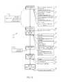
- FIG. 1Cis a flow diagram 172 illustrating a general method for forming a DDC transistor having an enhanced body coefficient and reduced variability in threshold voltage (a Vt), in accordance with various embodiments.
- the method illustrated in FIG. 1Cis intended to be general and broad in its description, and more detailed embodiments and examples are set forth below.
- Each block in the flow diagramis illustrated and described in further detail below, in conjunction with the various alternatives associated with each block illustrated in FIG. 1C .
- step 174the process begins at well formation, which can include one or more different process steps in accordance with different embodiments.
- the well formation step 174includes the steps for forming the screening region 112 , the threshold voltage set region 111 (if present), and the substantially undoped channel 110 .
- the well formation 174can be before or after the formation of an isolation structure (e.g., STI) 178 .
- an isolation structuree.g., STI
- the well formation 174can include forming the screening region 112 by implanting dopants into the P-well 114 , followed by an EPI pre-clean process that is followed by a blanket or selective EPI deposition. Various alternatives for performing these steps are illustrated in FIG. 1C .
- well formation 174can include a beam line implant of Ge/B (N), As (P), followed by an epitaxial (EPI) pre-clean process, and followed by a non-selective (blanket) EPI deposition, as shown in 174 A.
- the well formation 174can include using a plasma implant of B (N), As (P), followed by an EPI pre-clean, then a non-selective (blanket) EPI deposition, as shown in 174 B.
- the well formation 174can alternatively include a solid-source diffusion of B(N), As(P), followed by an EPI pre-clean, and followed by a non-selective (blanket) EPI deposition, as shown in 174 C.
- well formation 174can also include well implants, followed by in-situ doped selective EPI of B (N), P (P) as shown in 174 D.
- the well formationcan be configured with different types of devices in mind, including DDC transistors, legacy transistors, high V T transistors, low V T transistors, improved ⁇ V T transistors, and standard or legacy ⁇ V T transistors.
- DDC transistorsDDC transistors
- legacy transistorshigh V T transistors
- low V T transistorslow V T transistors
- improved ⁇ V T transistorsimproved ⁇ V T transistors
- standard or legacy ⁇ V T transistorsstandard or legacy ⁇ V T transistors.
- the screening region 110can have a dopant concentration between about 5 ⁇ 10 18 to 1 ⁇ 10 20 dopant atoms/cm 3 , with the selected dopant concentration dependent on the desired threshold voltage as well as other desired transistor characteristics.
- a germanium (Ge), carbon (C), or other dopant migration resistant layercan be incorporated above the screening region to reduce upward migration of dopants.
- the dopant migration resistant layercan be formed by way of ion implantation, in-situ doped epitaxial growth or other process. In certain embodiments, a dopant migration resistant layer can also be incorporated to reduce downward migration of dopants.
- a threshold voltage set region 111is positioned above the screening region 112 .
- the threshold voltage set region 111can be either adjacent to, incorporated within or vertically offset from the screening region.
- the threshold voltage set region 111is formed by delta doping, controlled in-situ deposition, or atomic layer deposition.
- the threshold voltage set region 111can be formed by way of controlled outdiffusion of dopant material from the screening region 112 into an undoped epitaxial layer, or by way of a separate implantation into the substrate following formation of the screening region 112 , before the undoped epitaxial layer is formed.
- the threshold voltage set region 111can have a dopant concentration between about 1 ⁇ 10 18 dopant atoms/cm 3 and about 1 ⁇ 10 19 dopant atoms per cm 3 .
- the threshold voltage set region 111can have a dopant concentration that is approximately less than half of the concentration of dopants in the screening region 112 .
- an over-layer of the channelis formed above the screening region 112 and threshold voltage set region 111 by way of a blanket or selective EPI deposition (as shown in the alternatives shown in 174 A-D), to result in a substantially undoped channel region 110 of a thickness tailored to the technical specifications of the device.
- the thickness of the substantially undoped channel region 110ranges from approximately 5-25 nm, with the selected thickness based upon the desired threshold voltage for the transistor.
- a blanket EPI deposition stepis performed after forming the screening region 112 , and the threshold voltage setting region 111 is formed by controlled outdiffusion of dopants from the screening region 112 into a portion of the blanket EPI layer, as described below.
- Dopant migration resistant layers of C, Ge, or the likecan be utilized as needed to prevent dopant migration from the threshold voltage set region 111 into the substantially undoped channel region 110 , or alternatively from the screening region 112 into the threshold voltage set region 111 .
- dopant migration resistant layersIn addition to using dopant migration resistant layers, other techniques can be used to reduce upward migration of dopants from the screening region 112 and the threshold voltage set region 111 , including but not limited to low temperature processing, selection or substitution of low migration dopants such as antimony or indium, low temperature or flash annealing to reduce interstitial dopant migration, or any other technique to reduce movement of dopant atoms can be used.
- low temperature processingselection or substitution of low migration dopants such as antimony or indium, low temperature or flash annealing to reduce interstitial dopant migration, or any other technique to reduce movement of dopant atoms can be used.
- the substantially undoped channel region 110is positioned above the threshold voltage set region 111 .
- the substantially undoped channel region 110has a dopant concentration less than 5 ⁇ 10 17 dopant atoms per cm 3 adjacent or near the gate dielectric 128 .
- the substantially undoped channel region 110can have a dopant concentration that is specified to be approximately less than one tenth of the dopant concentration in the screening region 112 .
- the substantially undoped channel region 110may contain dopants so that the dopant concentration is elevated to above 5 ⁇ 10 17 dopant atoms per cm 3 adjacent or near the gate dielectric 128 or by using a very light dose of halo implants.
- the substantially undoped channel region 110remains substantially undoped by avoiding the use of high dosage halo or other channel implants.
- STI formation 178which, again, can occur before or after well formation 174 , can include a low temperature trench sacrificial oxide (TSOX) liner, which is formed at a temperature lower than 900° C. as shown by 178 A.
- TSOXtrench sacrificial oxide
- a gate stackcan be formed or otherwise constructed above the substantially undoped channel region 110 in a number of different ways, from different materials, and of different work functions.
- One optionis a Poly/SiON gate stack 180 A.
- Another optionis a gate-first process 1808 that includes SiON/Metal/Poly and/or SiON/Poly, followed by High-K/Metal Gate.
- a gate-last process 180 Cincludes a high-K/metal gate stack wherein the gate stack can either be formed with “Hi-K first-Metal gate last” flow or and “Hi-K last-Metal gate last” flow.
- 180 Dis a metal gate that includes a tunable range of work functions depending on the device construction.
- the metal gate materials for n-channel MOS (NMOS) and p-channel MOS (PMOS)are selected to near mid-gap, to take full advantage of the DDC transistor.
- NMOSn-channel MOS
- PMOSp-channel MOS
- metal gate materialscan be switched between NMOS and PMOS pairs as a way to attain the desired work functions for given devices.
- a gate stackmay be formed or otherwise constructed above the substantially undoped channel region 110 in a number of different ways, from different materials including polysilicon and metals to form what is known as “high-k metal gate”.
- the metal gate process flowmay be “gate first” or “gate last”.
- the metal gate materials for NMOS and PMOSare selected to near mid-gap, to take full advantage of the DDC transistor.
- traditional metal gate work function band-gap settingsmay also be used.
- metal gate materialscan be switched between NMOS and PMOS pairs as a way to attain the desired work functions for given devices.
- source/drain portionsmay be formed.
- the extension portionsare implanted, followed by additional spacer formation and then implant or, alternatively, selective epitaxial deposition of deep source/drain regions.
- Source/Drain tipscan be implanted.
- the dimensions of the tipscan be varied as required, and will depend in part on whether gate spacers (SPGR) are used.
- SPGRgate spacers
- Source/Drain tipsare not formed (step 182 A), and there may be no tip implant.
- the source 104 and drain 106can be formed preferably using conventional processes and materials such as ion implantation ( 184 A) and in-situ doped epitaxial deposition ( 184 B).
- ion implantation184 A
- in-situ doped epitaxial deposition184 B
- PMOS or NMOS selective EPI layerscan be formed in the source and drain regions as performance enhancers for strained channels.
- Source 104 and drain 106can further include raised and/or recessed source/drains, asymmetrically doped, counter-doped or crystal structure modified source/drains, or implant doping of source/drain extension regions according to LDD (lightly doped drain) techniques, provided that the thermal budget for any anneal steps be within the boundaries of what is required to keep the screening region 112 and threshold voltage setting region 111 substantially intact.
- LDDlightly doped drain
- a metal gateis formed in accordance with a gate last process.
- Step 186is optional and may be performed only for gate-last processes ( 186 A).
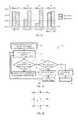
- Integrated circuit device 200 -Acan be a latch type circuit for storing complementary data values on storage nodes SN1/SN2.
- Integrated circuit device 200 -Acan include p-channel transistors 235 / 240 having sources connected to a first power supply node 291 , and gates and drains that cross-coupled between storage nodes (SN1/SN2). That is a gate of transistor 235 can be connected to node SN1, while its drain is connected to node SN2, and a gate of transistor 240 can be connected to node SN2, while its drain is connected to node SN1.
- Integrated circuit device 200 -Acan also include n-channel transistors 245 / 250 having sources connected to a second supply node VSS, and gates and drains that cross-coupled between storage nodes (SN1/SN2).
- a power supply circuit 215can provide a first power supply voltage VDD to supply node 291 , as well as a body bias voltage VBN to bodies of n-channel transistors 245 / 250 .
- Body bias voltage VBNcan be different than a second power supply voltage VSS.
- FIG. 2A-1shows n-channel transistors 245 / 250 that can be included in the embodiment of FIG. 2A-0 .
- N-channel transistors 245 / 250can have a highly doped screening region 212 , as described herein or equivalents.
- transistors 245 / 250can include any of: a threshold voltage set region 211 , SDEs 232 , a substantially undoped channel 210 / 254 (with or without SDEs), or a lightly doped channel 264 (such as that for an SDC transistor as described herein, or equivalents).
- n-channel transistors 245 / 250can match one another, and take the form of any of: DDC transistors, SDC transistors, or analog undoped channel transistors, as described herein, or an equivalent.
- P-channel transistors 235 / 240can take various forms, including but not limited to DDC transistors, SDC transistors, analog undoped channel transistors, or legacy transistors, as described herein, or an equivalent.
- conductivities of the integrated circuit device of FIG. 2A-0can be switched, with p-channel transistors having a highly doped screening region, and the n-channel transistors having any of various forms, including legacy transistors.
- Integrated circuit 200 -Bis a static random access memory (SRAM) array that may include a number of SRAM cells, including SRAM cells arranged in multiple rows and columns. For ease of discussion, however, only two SRAM cells 205 and 210 are illustrated and discussed along with the associated column power supplies 215 and 220 to generate the applied power supply and other voltages.
- the SRAM cells embodied at 205 and 210are implemented using DDC transistors.
- the SRAM cell 205includes a pair of pass-gate DDC transistors 225 and 230 , a pair of pull-up DDC transistors 235 and 240 , and a pair of pull-down DDC transistors 245 and 250 .
- the pass-gate DDC transistors 225 and 230 , and the pull-down DDC transistors 245 and 250are typically n-channel (referred to herein as NMOS) transistors.
- the pass-gate DDC transistors 225 and 230couple a pair of data lines BL0 and BLN0, also referred to as “bit lines”, to storage nodes SN1 and SN2 respectively, where the voltages at nodes SN1 and SN2 are inversely related.
- the pull-down DDC transistors 245 and 250couple a power supply VSS, usually the ground voltage of the circuit, to the storage nodes SN1 and SN2 respectively.
- the pull-up DDC transistors 235 and 240are typically p-channel (referred to herein as PMOS) transistors that couple the positive power supply VDDCOL0 to the storage nodes SN1 and SN2 respectively.
- the substrates of the NMOS transistorscan be coupled to a power supply voltage VBNCOL0, and the substrates of the PMOS transistors can be connected to a power supply voltage VBPCOL0, if a substrate bias voltage is applied to the NMOS and PMOS transistors respectively.
- SRAM cell 210is similar to SRAM cell 205 , and includes a pair of pass-gate DDC transistors 255 and 260 , a pair of pull-up DDC transistors 265 and 270 , a pair of pull-down DDC transistors 275 and 280 , storage nodes SN3 and SN4, bit lines BL1 and BLN1, and power supplies VDDCOL1 and VBPCOL1.
- the n-channel body bias voltages VBNCOL0 and VBNCOL1can be the same, such that all the n-channel body bias voltages can be connected to the same power supply voltage.
- the p-channel body bias voltages VBPCOL0 and VBPCOL1can be the same, such that all the p-channel body bias voltages can be connected to the same power supply voltage.
- each column of the SRAM 200 -Bincludes a column power supply block that supplies the power supply voltage for the corresponding column.
- the column power supply block 215supplies the body bias voltages VBPCOL0, VBNCOL0, and the power supply voltage VDDCOL0.
- the column power supply block 220supplies the body bias voltages VBPCOL1, VBNCOL1, and power supply voltage VDDCOL1.
- Each column power supply blockindependently controls the power supply voltage VDDCOL0/1, PMOS pull-up transistor body bias voltage VBPCOL0/1, and the NMOS transistor body-bias voltage VBNCOL0/1 supplied to each column such that each column can receive different power supply and body bias voltages.
- the column power supply blockcan provide different power supply voltages and body bias voltages to a given column at different times, or during different modes of operation.
- the SRAM cell shown in FIG. 2Bcan retain its state indefinitely as long as the power supply voltage (VDDCOL0/1) is sufficient to operate the cell correctly, i.e., the power supply voltage exceeds some V DDmin .
- the SRAM cell 205includes two cross-coupled inverters consisting of the pair of transistors 235 and 245 , and 240 and 250 . The two inverters operate to reinforce the stored charge on storage nodes SN1 and SN2 continuously, such that the voltages at each of the two storage nodes are inverted with respect to one another. When SN1 is at a logical “1”, usually a high voltage, SN2 is at a logical “0”, usually a low voltage, and vice versa.
- a write operationcan be performed to store data in a selected SRAM cell, and a read operation can be performed to access stored data in a selected SRAM cell.
- datais stored in a selected SRAM cell, e.g. SRAM cell 205 , during a write operation by placing complementary write data signals on the two bit lines BL0 and BLN0, and placing a positive voltage (VWL) on the word line WL connected to the gate of the pass-gate transistors 225 and 230 , such that the two bits lines BL0/BLN0 are coupled to the storage nodes SN1 and SN2, respectively.
- VWLpositive voltage
- the write operationis successful when the write data signals on the two bit lines overcome the voltages on the two storage nodes (if they are at opposite states to the write data) and modify the state of the SRAM cell.
- the cell writeis primarily due to the bit line driven low overpowering the opposing PMOS pull-up transistor via the pass-gate transistor (e.g., 240 being overpowered by BL0 via pass-gate 225 ).
- the relative strength ratio of the NMOS pass-gate transistor to the corresponding PMOS pull-up transistorcan be important to maximizing the write margin.
- datais accessed from a selected SRAM cell, e.g. SRAM cell 205 , during a read operation by precharging the two bit lines BL0 and BLN0 to a positive voltage, such as the positive power supply voltage VDDCOL0, and placing a positive voltage VWL on the word line WL such that the pass-gate transistors 225 and 230 allow the storage nodes SN1 and SN2 to be coupled to the bit lines BL0 and BLN0, respectively.
- the SRAM cell 205drives complementary read data signals onto the bit lines BL0 and BLN0, and a resulting read current pulls one of the two bit lines low in accordance with the stored state of the SRAM cell 205 .
- the differential voltage on the bit lines BL0 and BLN0can be sensed using a differential sense amplifier (not shown) that senses and amplifies the differential voltage signal on the bit lines.
- the output of the sense amplifieris subsequently output as the read data for the selected SRAM cell.
- Embodiments of SRAM cells using DDC transistorscan have enhanced performance characteristics as compared to SRAM cells using conventional MOSFETs.
- the DDC transistorscan have lower threshold voltage variation, i.e., lower ⁇ V T
- the DDC transistorshave higher I eff and higher body coefficient.
- SRAM cells using DDC transistorscan be designed more aggressively, in other words, with tighter design corners compared with the design corners using conventional MOSFETs.
- SRAM cells using DDC transistorscan therefore be reliably designed to have (1) enhanced read stability that can be measured as enhanced read static noise margin, as well as lower SRAM minimum operating voltage V DDmin ; (2) enhanced write margin; (3) faster SRAM operation resulting from lower read current variability; all while enjoying (4) lower SRAM cell leakage.
- FIG. 3Ashows a hybrid SRAM 300 having hybrid SRAM cells ( 305 and 310 ) that use both DDC transistors and legacy transistors, in accordance with one embodiment.
- the SRAM cell 305uses a pair of legacy PMOS transistors 335 and 340 as pull-up transistors.
- the SRAM cell 305also uses a pair of DDC NMOS transistors 345 and 350 as pull-down transistors, and a pair of DDC NMOS transistors 325 and 330 as pass-gate transistors.
- SRAM cell 305includes storage nodes SN1 and SN2, which are coupled to data lines BLN0 and BLN1 using the pass-gate DDC NMOS transistors 325 and 330 .
- SRAM cell 310is similar, and includes a pair of pass-gate DDC NMOS transistors 355 and 360 , a pair of pull-up legacy PMOS transistors 365 and 370 , and a pair of pull-down DDC NMOS transistors 375 and 380 .
- SRAM cell 310includes storage nodes SN3 and SN4, which are coupled to data lines BL1 and BLN1 using the pass-gate DDC NMOS transistors 355 and 360 .
- Column power supplies 315 and 320can provide various voltages to columns that include SRAM cells 305 and 310 , respectively. Such voltages can include high power supply voltages VDDCOL0/1, n-channel body bias voltages VBNCOL0/1, and p-channel body bias voltages VBPCOL0/1. Power supplies 315 / 320 can be coupled to the substrates of the legacy PMOS transistors 335 / 340 and 365 / 370 , respectively, if a substrate bias voltage (VBPCOL0/1) is applied to these transistors.
- VBPCOL0/1substrate bias voltage
- Power supplies 315 / 320can be coupled to the substrates of the DDC NMOS transistors 325 / 345 / 350 and 355 / 375 / 380 , respectively, if a substrate bias voltage (VBNCOL0/1) is applied to these transistors.
- the sizing of transistors in an SRAM cellcan be determined by a tradeoff between sizing for read static noise margin (SNM) and sizing for write margin. Using DDC transistors in an SRAM cell can improve both the read SNM and write margin for the SRAM cell.
- Hybrid SRAM cells 305 and 310have enhanced performance characteristics because of the DDC NMOS transistor characteristics.
- the DDC NMOS transistorscan exhibit a higher current drive as compared to conventional MOSFETs, when a low voltage is being applied to the gate and the drain to source voltage is less than VGS ⁇ Vt of the transistor, i.e., such that the transistor is operating in the linear region.
- the higher current drive of the DDC NMOS transistorscontributes to an enhanced Read SNM.
- the DDC NMOS pass gate transistor of the hybrid SRAM cellhas an increased body bias voltage that results from the rise in the storage node voltage during the read operation. Therefore, the enhanced body coefficient of the DDC NMOS transistor results in a DDC NMOS pass gate transistor with reduced current drive capability.
- the combination of the enhanced drive capability of the pull down transistor, and the reduced drive capability of the pass gate transistorresults in an increased read SNM and increased cell stability.
- the hybrid SRAM cells 305 and 310 shown in FIG. 3Ausing DDC NMOS pass-gate and DDC NMOS pull-down transistors provides increased read SNM, and therefore, a lower read failure rate.
- the DDC NMOS transistorshave a lower variability of threshold voltage, i.e., lower ⁇ VT and lower transistor matching coefficient AVT, the hybrid SRAM cells 305 and 310 can have a lower VDDmin than a conventional SRAM cell that uses similarly sized conventional NMOS and PMOS transistors.
- FIG. 3Bshows a hybrid SDC SRAM 301 having hybrid SDC SRAM cells ( 306 and 311 ) that used both SDC transistors and legacy transistors, in accordance with one embodiment.
- the SRAM cell 306uses a pair of SDC NMOS transistors 346 and 351 as pull-down transistors, and a pair of SDC NMOS transistors 326 and 331 as pass-gate transistors.
- the SRAM cell 306also uses a pair of legacy PMOS transistors 335 and 340 as pull-up transistors.
- SRAM cell 311is similar, and includes a pair of pass-gate SDC NMOS transistors 356 and 361 , a pair of pull-down SDC NMOS transistors 376 and 381 , and a pair of pull-up legacy PMOS transistors 365 and 370 .
- a hybrid SDC SRAM cell 306 / 311can have enhanced performance characteristics compared with SRAM using conventional transistors because of the SDC transistor characteristics. These improved transistor characteristics are similar to the enhanced characteristics of a hybrid SRAM cell using DDC and legacy transistors (e.g., FIG. 3A ), and therefore can be designed to tighter design corners compared with conventional MOSFETs, to result in performance benefits such as, increased read SNM, increased cell stability, lower read and write failure rates, and lower VDDmin.
- Using SDC transistors in an SRAM cellcan improve both the read SNM and write margin for the SRAM cell.
- each column of the SRAMs 300 and 301can include a column power supply 315 / 320 that supplies a power supply voltage (VDDCOL0/1) for the corresponding column.
- column power supplies 315 / 320can also provide body bias voltages to one or both types of transistors in an SRAM cell.
- column power supply 315in addition to power supply VDDCOL0, column power supply 315 can provide n-channel body bias voltage VBNCOL0 and p-channel body bias voltage VBPCOL0.
- column power supply 320can provide n-channel body bias voltage VBNCOL1 and p-channel body bias voltage VBPCOL1.
- the n-channel body bias voltages VBNCOL0 and VBNCOL1can be the same, such that all the n-channel body bias voltages can be connected to the same power supply voltage.
- the p-channel body bias voltages VBPCOL0 and VBPCOL1can be the same, such that all the p-channel body bias voltages can be connected to the same power supply voltage.
- Column power supplies 315 and 320can either be same or different. That, column power supplies 315 / 320 can operate together to provide power supply and/or body bias voltages, or each column power supply can independently control its power supply voltage and/or body bias voltage(s). In addition, in some embodiments the column power supplies 315 / 320 can provide different power supply voltages and/or body bias voltages to the same column at different times, or during different modes of operation. For example, the column power supplies 315 / 320 can generate power supply and body bias voltages that are identical for read and write operations, or they can generate voltages that are different for read and write operations, depending on the embodiment.
- hybrid SRAM celland the hybrid SDC SRAM cells described above, alternative embodiments of hybrid SRAM cells that use two or more different types of transistors can also provide better performance characteristics. Such embodiments can include SRAM cells that use both DDC and SDC transistors. In addition, embodiments that include SDC SRAM cells that use only SDC transistors can also provide similar advantages.
- transistor body bias voltagescan be applied globally, i.e., to the entire integrated circuit, or to all devices in the SRAM arrays, as well as by column as shown, in order to allow precise electrically controlled targeting of the leakage and other SRAM characteristics.
- the enhanced body effect of the DDC and SDC transistorsfacilitates such wider use of body bias compared to conventional MOSFETs.
- the body bias voltagescan be applied to only one of the transistors types in the integrated circuit or the SRAM array. For example, the body bias voltages can be applied to only the PMOS transistors, or to only the NMOS transistors in the integrated circuit or the SRAM array.
- the body bias voltages applied to the integrated circuit or the SRAM arraycan either be fixed throughout the IC operation and/or lifetime, or may be varied dynamically in order to meet target operational characteristics of the SRAM as described below.
- This electrically controlled targeting of the leakage and other SRAM device characteristicscan be used either alone or in combination with additional adjustments that can be obtained due to the structure and processing of the specific transistors and/or the operating conditions of the transistors.
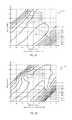
- FIG. 3Cshows read and write failure rates for an SRAM cell at different stages of the design process to reduce VDDmin, in accordance with one embodiment.
- Four sets of read and write failure ratesare shown in FIG. 3C corresponding to four SRAM cells—(1) a baseline SRAM cell with substantially balanced read and write failure rates; (2) a SRAM cell with 20% AVT improvement for the NMOS transistors; (3) a SRAM cell with 30% AVT improvement for the NMOS transistors; and (4) a SRAM cell with the PMOS threshold voltage increased by 35 mV and a 30% AVT improvement for NMOS.
- FIG. 3Calso shows the VDDmin for each of these SRAM cells.
- the baseline SRAM cellcan be a SRAM cell implemented using legacy PMOS and NMOS transistors only, and the SRAM cells with improved NMOS AVT can be hybrid SRAM cells that use NMOS DDC transistors and PMOS legacy transistors as described with reference to FIG. 3A above.
- the pass-gate, pull-up, and pull-down transistors of the hybrid SRAM cellshave approximately the same drawn sizes as corresponding transistors of the baseline cell.
- FIG. 3Cshows that the baseline SRAM cell can be designed to operate at a lower VDDmin by converting it to a hybrid SRAM cell, where the NMOS transistors in the baseline SRAM cell are substituted with NMOS DDC transistors with improved AVT. Improving the NMOS AVT for the SRAM can improve the read SNM and write margin for a predetermined value of the power supply voltage VDD, resulting in lower read and write failures, and a lower VDDmin.
- FIG. 3Calso shows that as VDDmin is reduced, the rates at which read failures and write failures increase can differ, and therefore, the SRAM cell can become either read limited (i.e., read failure rate higher than the write failure rate) or write limited (write failure rate higher than the read failure rate).
- FIG. 3Cshows that the SRAM cells with 20% and 30% NMOS AVT improvement are write limited at a VDDmin of 0.72V and 0.69V respectively. It is noted that if the hybrid SRAM cell obtained by converting the baseline SRAM cell has a read and write failure rate that is sufficiently low to provide a desired yield, the design method described herein can provide an improved target SRAM cell that has a lower VDDmin, without providing further reductions in the read and/or write failure rates. This can be observed in FIG. 3C , where the design method results in write failure rates for 3 C( 1 ) and 3 C( 4 ) that are substantially identical, but results in a VDDmin reduction of approximately 0.1V (i.e. from 0.77V to 0.67V).
- the design method described hereincan provide an improved target SRAM call having an acceptable (i.e., less that the target) failure rate as well as a lower VDDmin.
- a read or write limited SRAM cellcan be further designed to operate at a lower VDDmin by retargeting the PMOS and/or the NMOS threshold voltage.
- the SRAM cell corresponding to a VDDmin of 0.69V(( 3 ) in FIG. 3C ) can be designed by way of weakening the legacy PMOS pull-up transistors, i.e., by increasing the PMOS threshold voltage, resulting in further reduction of VDDmin.
- the SRAM cellcan also be designed by way of retargeting the threshold voltage of the NMOS transistors in the SRAM cell. As shown in FIG.
- increasing the PMOS threshold voltagecan provide a balanced SRAM cell that has substantially similar read and write failure rates since the read failure rate can increase and the write failure rate can decrease with increases in the PMOS threshold voltage.
- the total cell failure rateis reduced. This also reflects a lower failure rate for the current power supply voltage at which these failure rates are measured, and therefore, the VDDmin for the SRAM can be reduced further at the required or desired yield.
- Some embodiments of the hybrid SRAM cell using DDC NMOS transistors (for the pull-down and pass-gate transistors) and legacy PMOS pull-up transistorscan use only one type of gate metal (i.e., the legacy PMOS transistor gate metal).
- a single metal hybrid SRAM cellcan require fewer processing steps and mask layers for fabrication, and therefore, it can have a higher yield than a SRAM cell that requires the use of two different gate metals for the NMOS and PMOS transistors.
- the NMOS DDC transistorcan be advantageously used in the single metal hybrid SRAM cell because the threshold voltage of the DDC transistor can be set by the screening region dopant concentration, the threshold set region dopant concentration, and the thickness of the epitaxial layer, as discussed above.
- the threshold voltage of the DDC NMOS transistorcan be set to a desired target value even though the gate metal that is used is the PMOS gate metal having a PMOS workfunction.
- Similar embodiments of the hybrid SDC SRAM cellcan be implemented using a single gate metal, and can provide similar advantages.
- Various methods in accordance with the embodiments discussed belowcan be used to generate a target SRAM cell based on a source SRAM cell, where the target SRAM cell is a hybrid SRAM that uses DDC NMOS transistors or SDC NMOS transistors, and the source SRAM cell uses conventional MOSFETs, e.g., MOSFETs having dopants in the channel and/or halo implants.
- the target SRAM cellis designed to be a drop-in replacement for the source SRAM cell.
- the target SRAM cellcan have the same area as the source SRAM cell, and each of the DDC/SDC transistors in the target SRAM cell can have the same size as the corresponding transistor in the source SRAM cell.
- the target SRAM cellcan be fabricated without making any modifications to the Graphic Data System (GDS) format information corresponding to the source SRAM cell.
- the target SRAM cellcan be fabricated using the same GDS format information as the source SRAM cell but the GDS information can be resized to produce the master or direct write information for the migrated SRAM cell.
- GDSGraphic Data System
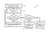
- FIG. 4Aillustrates a flow diagram of a method 400 for designing a target SRAM cell based on a source SRAM cell, for which the NMOS and PMOS threshold voltages are retargeted, where the target SRAM cell has a lower VDDmin than the source SRAM cell, in accordance with one embodiment.
- VDDmincan be determined as the lowest value of VDD at which all, or a predetermined percentage of the SRAM cells can function properly for both read and write operation, i.e. the SRAM cells have sufficient read SNM, read current, and write margin.
- the method 400designs the NMOS and PMOS transistor threshold voltages (hereinafter referred to as “V TN ” and “V TP ” respectively) of the transistors in the source SRAM cell to obtain the target SRAM cell.
- Step 405determines relevant characteristics of the source SRAM cell including the size of one or more transistors in the source SRAM cell, as well as the threshold voltages V TN and V TP of the NMOS and PMOS transistors in the source SRAM cell. Step 405 can also determine additional parameters for the transistors in the source SRAM cell, e.g., the threshold voltage variation characterized by AVT or ⁇ VT, drain induced barrier lowering (DIBL), drive current, leakage current, etc. In addition, step 405 determines the VDDmin of the source SRAM cell.
- the source SRAM cellcan be any SRAM cell, including the SRAM cell embodiments discussed above with reference to FIGS. 3 A/B.
- Step 410determines the new SRAM cell failure rates in response to changing either one or both the threshold voltages V TN and V TP , when the SRAM cell is operating at a high power supply voltage of VDDmin.
- the SRAM cell failure ratecan be determined as the read and write failure rates at the power supply voltage VDDmin currently under evaluation.
- the failure ratesare calculated for a number of candidate V TN and V TP points during step 410 that correspond to one or more of the following changes to V TN and V TP :
- FIG. 4Bis a graph showing a range of candidate V TN and V TP points with reference to current starting point V TN and V TP , when the method of FIG. 4A is implemented.
- the failure ratescan be determined at fewer than the eight points shown in the figure.
- the failure ratescan be determined for candidate V TN and V TP corresponding to only the corners (i.e. points b, f, d, and h in FIG. 4B ), or only the edges (i.e. points a, c, e, and g).
- the value of the step size ⁇ V Tcan be fixed, e.g. it can be set at 5 mV.
- a variable step sizecan be used, where a large step can be used initially, and the step size can be reduced as the impact of changing V T on the failure rate shows that large steps may not allow further optimization of the SRAM cell within the failure limit and failure criterion. Therefore, if the failure rates corresponding to the candidate V TN and V TP are higher than the current failure rate (at V TN and V TP ), then the step size can be reduced, and the response of the SRAM cell can be determined for the reduced step size. Thus, the (V TN , V TP ) space can initially be traversed more quickly, allowing a faster and more efficient design for an SRAM cell.
- the step sizecan be varied as needed using alternative algorithms that can reduce the number of iterations required to arrive at the new target SRAM cell.
- step 415analyzes the SRAM cell failure rates obtained in step 410 to determine if any of the failure rates corresponding to the candidate V TN and V TP points in step 410 are lower than the failure rate at (V TN , V TP ), and if leakage and other performance constraints are satisfied. If one or more of the failure rates corresponding to the candidate V TN and V TP are lower (branch 460 labeled Y) and at least one of these candidate (V TN , V TP ) points satisfy the leakage and performance constraints, execution of the method 400 continues to step 420 . Otherwise execution proceeds along branch 465 labeled “N”, and execution of the method 400 continues to step 425 .
- step 415determines whether the leakage constraints are satisfied by determining whether the leakage current for the SRAM cell with the candidate V TN and V TP is less than a predetermined maximum leakage current at a nominal or maximum value of the power supply voltage VDD. Similarly, step 415 can determine whether other performance characteristics are satisfied at a nominal or maximum value of the power supply voltage VDD.
- candidate (V TN , V TP ) points that have been evaluated and rejected during steps 410 and 415i.e., candidate (V TN , V TP ) points rejected in favor of a candidate (V TN , V TP ) point having a lower failure rate, are stored such that these candidate points are evaluated only once during successive steps of the design method 400 .
- reducing V TN and/or V TPcan reduce VDDmin but the read/write failure rates can change.
- the impact of reducing V TN and/or V TP on the read/write failure ratescan be dependent on the state of the SRAM cell before the threshold voltages are changed, and whether the SRAM cell is read limited, write limited, or balanced prior to changing the threshold voltages.
- Reducing V TN and V TPcan increase the leakage.
- the leakagecan be reduced by using transistors with improved AVT that can reduce the average cell leakage, which is proportional to the SRAM array leakage (the leakage that impacts the integrated circuit).
- SRAM arrays using DDC transistorscan have a lower leakage at the same V TN and V TP .
- the increasing leakagecan still limit the SRAM operating range as it limits the range of V TN and V TP that can be used.
- increasing V TNcan reduce the read current Iread thereby reducing read performance.
- improving the AVTcan reduce the impact of read current degradation as well.
- Step 420modifies V TN and V TP of the SRAM cell to improve the failure rate, and determines the failure rate of the modified SRAM cell.
- step 420can analyze the response of the SRAM cell to the candidate V TN and V TP in step 410 described above and can select a new V TN and V TP in accordance with one of the following approaches:
- V TN and V TP modificationfrom the candidate V TN and V TP points analyzed in step 410 above
- the read failure ratebeing substantially similar to the write failure rate
- step 420moves the point under analysis for the SRAM cell failure rates towards candidate V TN and V TP that result in the read failure rate being substantially similar to the write failure rate (i.e., the read or write SRAM failure rates may not be calculated for all of the eight possible candidate V TN and V TP points listed for step 410 above), and step 415 selects the candidate V TN and V TP point that results in the SRAM cell having more balanced read and write failures.
- the total failure rate of the SRAM cellcan be the sum of the read failure rate and the write failure rate. In an alternative embodiment, the total failure rate can be the maximum failure rate, which is the higher of the read failure rate and the write failure rate.
- Step 425compares the failure rate of the SRAM cell to a predetermined maximum allowed failure rate. If the failure rate is less than the maximum allowed failure rate, execution of method 400 continues along branch 470 (labeled “Y”), the current values of VDDmin, V TN , and V TP are saved (step 430 ), control is transferred to step 435 and further iterations within the design process are performed as illustrated in the flow diagram of method 400 . If the failure rate is greater than the maximum allowed failure rate, execution of method 400 continues along branch 475 (labeled “N”), control is transferred to step 440 .
- Step 435reduces VDDmin by a predetermined amount ⁇ VDD, and transfers control to step 410 for continued design of the SRAM cell.
- the value of the step size ⁇ VDDcan be fixed, e.g. it can be set at 5 mV.
- a variable step sizecan be used, where a large step can be used initially, and the step size can be reduced as the impact of changing VDD on the failure rate shows that large steps may not allow further modification of the design of the SRAM cell within the failure limit and failure criterion. Therefore, if the failure rates corresponding to the modified VDD are higher than the current failure rate (at the saved VDD), then the step size can be reduced, and the response of the SRAM cell can be determined for the reduced step size.
- the VDD rangecan initially be traversed more quickly, allowing for a faster design method that arrives to substantially the same optimized SRAM cell in fewer design steps.
- the VDD step sizecan be varied using alternative algorithms that can reduce the number of iterations required to arrive at the new target SRAM cell.
- step 425if the failure rate is greater than the maximum allowed failure rate, execution of the method 400 continues along branch 475 (labeled “N”), the saved values of VDDmin, V TN , and V TP are recovered (step 440 ), and the target SRAM cell is obtained (step 445 ).
- the substrate bias voltage for the DDC NMOS transistorscan be changed by a step size ⁇ V BN and the resulting failure rates, leakage, and performance characteristics are reevaluated.
- the substrate bias voltage for the NMOS DDC transistorcan be increased until one or more of the modified (V TN , V TP ) points satisfy the failure rate, leakage, and performance constraints.
- the substrate bias voltage for only the PMOS transistors, only the NMOS transistors, or both the PMOS and NMOS transistorscan be either increased or decreased until the SRAM cell satisfies the failure rate, leakage, and performance constraints.
- FIG. 5Ais a contour plot 500 showing bit failure rates for a fixed VDD (0.7V), and a possible sequence of V TN and V TP offsets that can be traversed in order to obtain a target SRAM cell.
- the trajectory 505illustrates a possible sequence of V TN and V TP offsets that can be traversed during the design of the SRAM cell by one of the method embodiments described above.
- the trajectory 505starts at an initial offset of (0, 0) corresponding to the source SRAM with no modifications to V TN and V TP .
- the end point of the trajectory 505represents the offsets or modifications to V TN and V TP that provide a target SRAM cell for VDD of 0.7V.
- FIG. 5Bis a contour plot 510 of bit failure rates of the target SRAM cell obtained at VDD of 0.7V, when VDD is reduced to 0.69V.
- the trajectory 515shows a possible sequence of V TN and V TP offsets that can be traversed in order to obtain a design for a target SRAM cell at VDD of 0.69V. If the failure rate of the target SRAM cell at 0.69V VDD (corresponding to the end point of the trajectory 515 ) is less than the maximum allowed failure rate, and if leakage and other performance characteristics are satisfied, VDD can be reduced further and the design process can be continued, in accordance with the method embodiments described above.
- the various methods for designing the SRAM cell described abovecan be used to set the transistor W/L and/or the threshold voltages V TP and V TN for the transistors used in the target SRAM cell to design the SRAM with reduced VDDmin.
- the transistor W/Lcan be modified as part of the design such that no GDS changes are required, i.e. the transistor changes are made within a range that can be obtained by performing an optional GDS resizing.
- embodiments of the methods described abovecan be used to retarget the SRAM cell when the electrical parameters or characteristics of any of the transistors used in the SRAM cell are modified.
- Embodiments of the methods described abovecan be used to retarget SRAM cells using only legacy transistors, only DDC transistors, only SDC transistors, as well as hybrid SRAM cells, and hybrid SDC SRAM cells.
- the structures and methods of making the structuresallow for DDC or SDC transistors having an enhanced body coefficient as compared to conventional nanoscale devices.
- the response of the DDC/SDC transistorcan vary within a wider range to a change in the body bias voltage applied to the screening region.
- the enhanced body coefficient of the DDC/SDC transistorcan allow a broad range of ON-current and OFF-current that depends on the body bias voltage applied to the screening region, as compared to the body bias voltage applied to a conventional device.
- the DDC/SDC transistorshave a better AVT, i.e., a lower ⁇ V T than conventional devices.
- the lower ⁇ V Tprovides a lower minimum operating voltage VDD and a wider range of available nominal values of V T .
- the enhanced body coefficient of the DDC/SDC transistorcan also allow a broad range of threshold voltage that depends on the body bias voltage applied to the screening region, as compared to the body bias voltage applied to a conventional device.
- the screening regionallows effective body biasing for enhanced control of the operating conditions of a device or a group of devices to be set by controlling the applied body bias voltage.
- different operating conditionscan be set for devices or groups of devices as result of applying different body bias voltages.
- Electronic devicesthat include the disclosed transistor structures or are manufactured in accordance with the disclosed processes can incorporate die configured to operate as “systems on a chip” (SoC), advanced microprocessors, radio frequency, memory, and other die with one or more digital and analog transistor configurations, and are capable of supporting a wide range of applications, including wireless telephones, communication devices, “smart phones”, embedded computers, portable computers, personal computers, servers, and other electronic devices.
- Electronic devicescan optionally include both conventional transistors and transistors as disclosed, either on the same die or connected to other die via motherboard, electrical or optical interconnect, stacking or through used of 3D wafer bonding or packaging. According to the methods and processes discussed herein, a system having a variety of combinations of analog and/or digital transistor devices, channel lengths, and strain or other structures can be produced.
Landscapes
- Engineering & Computer Science (AREA)
- Computer Hardware Design (AREA)
- Physics & Mathematics (AREA)
- Theoretical Computer Science (AREA)
- Microelectronics & Electronic Packaging (AREA)
- Evolutionary Computation (AREA)
- Geometry (AREA)
- General Engineering & Computer Science (AREA)
- General Physics & Mathematics (AREA)
- Insulated Gate Type Field-Effect Transistor (AREA)
Abstract
Description
Claims (11)
Priority Applications (1)
| Application Number | Priority Date | Filing Date | Title |
|---|---|---|---|
| US13/716,080US8819603B1 (en) | 2011-12-15 | 2012-12-14 | Memory circuits and methods of making and designing the same |
Applications Claiming Priority (2)
| Application Number | Priority Date | Filing Date | Title |
|---|---|---|---|
| US201161576254P | 2011-12-15 | 2011-12-15 | |
| US13/716,080US8819603B1 (en) | 2011-12-15 | 2012-12-14 | Memory circuits and methods of making and designing the same |
Publications (1)
| Publication Number | Publication Date |
|---|---|
| US8819603B1true US8819603B1 (en) | 2014-08-26 |
Family
ID=51358778
Family Applications (1)
| Application Number | Title | Priority Date | Filing Date |
|---|---|---|---|
| US13/716,080ActiveUS8819603B1 (en) | 2011-12-15 | 2012-12-14 | Memory circuits and methods of making and designing the same |
Country Status (1)
| Country | Link |
|---|---|
| US (1) | US8819603B1 (en) |
Cited By (5)
| Publication number | Priority date | Publication date | Assignee | Title |
|---|---|---|---|---|
| US20140173548A1 (en)* | 2012-09-17 | 2014-06-19 | Texas Instruments Incorporated | Tool For Automation Of Functional Safety Metric Calculation And Prototyping Of Functional Safety Systems |
| US20150171158A1 (en)* | 2010-11-03 | 2015-06-18 | Texas Instruments Incorporated | Low temperature coefficient resistor in cmos flow |
| US20150241511A1 (en)* | 2014-02-24 | 2015-08-27 | International Business Machines Corporation | System and method for managing semiconductor manufacturing defects |
| CN113221494A (en)* | 2020-01-21 | 2021-08-06 | 中芯国际集成电路制造(上海)有限公司 | Method for generating process angle analysis model in SRAM and method for determining process angle |
| US11113442B2 (en)* | 2017-09-28 | 2021-09-07 | Intel Corporation | Methods and apparatus for reducing reliability degradation on an integrated circuit |
Citations (469)
| Publication number | Priority date | Publication date | Assignee | Title |
|---|---|---|---|---|
| US3958266A (en) | 1974-04-19 | 1976-05-18 | Rca Corporation | Deep depletion insulated gate field effect transistors |
| US4000504A (en) | 1975-05-12 | 1976-12-28 | Hewlett-Packard Company | Deep channel MOS transistor |
| US4021835A (en) | 1974-01-25 | 1977-05-03 | Hitachi, Ltd. | Semiconductor device and a method for fabricating the same |
| US4242691A (en) | 1978-09-18 | 1980-12-30 | Mitsubishi Denki Kabushiki Kaisha | MOS Semiconductor device |
| US4276095A (en) | 1977-08-31 | 1981-06-30 | International Business Machines Corporation | Method of making a MOSFET device with reduced sensitivity of threshold voltage to source to substrate voltage variations |
| US4315781A (en) | 1980-04-23 | 1982-02-16 | Hughes Aircraft Company | Method of controlling MOSFET threshold voltage with self-aligned channel stop |
| US4518926A (en) | 1982-12-20 | 1985-05-21 | At&T Bell Laboratories | Gate-coupled field-effect transistor pair amplifier |
| US4559091A (en) | 1984-06-15 | 1985-12-17 | Regents Of The University Of California | Method for producing hyperabrupt doping profiles in semiconductors |
| US4578128A (en) | 1984-12-03 | 1986-03-25 | Ncr Corporation | Process for forming retrograde dopant distributions utilizing simultaneous outdiffusion of dopants |
| US4617066A (en) | 1984-11-26 | 1986-10-14 | Hughes Aircraft Company | Process of making semiconductors having shallow, hyperabrupt doped regions by implantation and two step annealing |
| US4662061A (en) | 1985-02-27 | 1987-05-05 | Texas Instruments Incorporated | Method for fabricating a CMOS well structure |
| EP0274278A1 (en) | 1987-01-05 | 1988-07-13 | Seiko Instruments Inc. | MOS field effect transistor and method of manufacturing the same |
| US4761384A (en) | 1986-06-10 | 1988-08-02 | Siemens Aktiengesellschaft | Forming retrograde twin wells by outdiffusion of impurity ions in epitaxial layer followed by CMOS device processing |
| US4780748A (en) | 1986-06-06 | 1988-10-25 | American Telephone & Telegraph Company, At&T Bell Laboratories | Field-effect transistor having a delta-doped ohmic contact |
| US4819043A (en) | 1985-11-29 | 1989-04-04 | Hitachi, Ltd. | MOSFET with reduced short channel effect |
| EP0312237A2 (en) | 1987-10-13 | 1989-04-19 | AT&T Corp. | Interface charge enhancement in delta-doped heterostructure |
| US4885477A (en) | 1987-06-08 | 1989-12-05 | U.S. Philips Corporation | Differential amplifier and current sensing circuit including such an amplifier |
| US4908681A (en) | 1980-04-30 | 1990-03-13 | Sanyo Electric Co., Ltd. | Insulated gate field effect transistor with buried layer |
| US4945254A (en) | 1986-03-19 | 1990-07-31 | The Secretary of State for Defence in Her Britannic Majesty's Government for the United Kingdom of Great Britain and Northern Ireland | Method and apparatus for monitoring surface layer growth |
| US4956311A (en) | 1989-06-27 | 1990-09-11 | National Semiconductor Corporation | Double-diffused drain CMOS process using a counterdoping technique |
| US5034337A (en) | 1989-02-10 | 1991-07-23 | Texas Instruments Incorporated | Method of making an integrated circuit that combines multi-epitaxial power transistors with logic/analog devices |
| US5144378A (en) | 1990-03-06 | 1992-09-01 | Fujitsu Limited | High electron mobility transistor |
| US5156989A (en) | 1988-11-08 | 1992-10-20 | Siliconix, Incorporated | Complementary, isolated DMOS IC technology |
| US5156990A (en) | 1986-07-23 | 1992-10-20 | Texas Instruments Incorporated | Floating-gate memory cell with tailored doping profile |
| US5166765A (en) | 1991-08-26 | 1992-11-24 | At&T Bell Laboratories | Insulated gate field-effect transistor with pulse-shaped doping |
| EP0531621A2 (en) | 1991-09-12 | 1993-03-17 | Pohang Iron & Steel Co., Ltd. | Process for formation of delta-doped quantum well field effect transistor |
| US5208473A (en) | 1989-11-29 | 1993-05-04 | Mitsubishi Denki Kabushiki Kaisha | Lightly doped MISFET with reduced latchup and punchthrough |
| US5294821A (en) | 1990-10-09 | 1994-03-15 | Seiko Epson Corporation | Thin-film SOI semiconductor device having heavily doped diffusion regions beneath the channels of transistors |
| US5298763A (en) | 1992-11-02 | 1994-03-29 | Motorola, Inc. | Intrinsically doped semiconductor structure and method for making |
| US5369288A (en) | 1992-05-08 | 1994-11-29 | Fujitsu Limited | Semiconductor device for switching a ballistic flow of carriers |
| US5373186A (en) | 1984-11-19 | 1994-12-13 | Max-Planck Gesellschaft Zur Foerderung Der Wissenschaften E.V. | Bipolar transistor with monoatomic base layer between emitter and collector layers |
| US5384476A (en) | 1979-08-25 | 1995-01-24 | Zaidan Hojin Handotai Kenkyu Shinkokai | Short channel MOSFET with buried anti-punch through region |
| US5426328A (en) | 1992-09-21 | 1995-06-20 | Siliconix Incorporated | BICDMOS structures |
| US5444008A (en) | 1993-09-24 | 1995-08-22 | Vlsi Technology, Inc. | High-performance punchthrough implant method for MOS/VLSI |
| EP0683515A1 (en) | 1994-05-17 | 1995-11-22 | Samsung Electronics Co., Ltd. | CMOS and method for manufacturing the same |
| US5552332A (en) | 1995-06-02 | 1996-09-03 | Motorola, Inc. | Process for fabricating a MOSFET device having reduced reverse short channel effects |
| US5559368A (en) | 1994-08-30 | 1996-09-24 | The Regents Of The University Of California | Dynamic threshold voltage mosfet having gate to body connection for ultra-low voltage operation |
| US5608253A (en) | 1995-03-22 | 1997-03-04 | Advanced Micro Devices Inc. | Advanced transistor structures with optimum short channel controls for high density/high performance integrated circuits |
| US5622880A (en) | 1994-08-18 | 1997-04-22 | Sun Microsystems, Inc. | Method of making a low power, high performance junction transistor |
| US5625568A (en) | 1993-12-22 | 1997-04-29 | Vlsi Technology, Inc. | Method and apparatus for compacting integrated circuits with standard cell architectures |
| US5624863A (en) | 1995-07-17 | 1997-04-29 | Micron Technology, Inc. | Semiconductor processing method of forming complementary N-type doped and P-type doped active regions within a semiconductor substrate |
| US5641980A (en) | 1995-06-16 | 1997-06-24 | Mitsubishi Denki Kabushiki Kaisha | Device having a high concentration region under the channel |
| US5663583A (en) | 1995-06-06 | 1997-09-02 | Hughes Aircraft Company | Low-noise and power ALGaPSb/GaInAs HEMTs and pseudomorpohic HEMTs on GaAs substrate |
| US5712501A (en) | 1995-10-10 | 1998-01-27 | Motorola, Inc. | Graded-channel semiconductor device |
| US5726562A (en) | 1995-09-07 | 1998-03-10 | Nec Corporation | Semiconductor device and power supply controller for same |
| US5726488A (en) | 1985-11-29 | 1998-03-10 | Hitachi, Ltd. | Semiconductor device having semiconductor elements formed in a retrograde well structure |
| US5731626A (en) | 1994-12-01 | 1998-03-24 | Lucent Technologies Inc. | Process for controlling dopant diffusion in a semiconductor layer and semiconductor layer formed thereby |
| US5736419A (en) | 1996-11-12 | 1998-04-07 | National Semiconductor Corporation | Method of fabricating a raised source/drain MOSFET using self-aligned POCl3 for doping gate/source/drain regions |
| US5754826A (en) | 1995-08-04 | 1998-05-19 | Synopsys, Inc. | CAD and simulation system for targeting IC designs to multiple fabrication processes |
| US5753555A (en) | 1995-11-22 | 1998-05-19 | Nec Corporation | Method for forming semiconductor device |
| US5756365A (en) | 1992-10-30 | 1998-05-26 | Kabushiki Kaisha Toshiba | Method of manufacturing MOS-type semiconductor device having electrode structure capable of coping with short-channel effects |
| US5763921A (en) | 1991-10-22 | 1998-06-09 | Mitsubishi Denki Kabushiki Kaisha | Semiconductor device including retrograde well structure with suppressed substrate bias effects |
| US5847419A (en) | 1996-09-17 | 1998-12-08 | Kabushiki Kaisha Toshiba | Si-SiGe semiconductor device and method of fabricating the same |
| US5856003A (en) | 1997-11-17 | 1999-01-05 | Taiwan Semiconductor Manufacturing Company, Ltd. | Method for forming pseudo buried layer for sub-micron bipolar or BiCMOS device |
| EP0889502A2 (en) | 1997-06-30 | 1999-01-07 | International Business Machines Corporation | Semiconductor structure with abrupt doping profile |
| US5861334A (en) | 1995-08-07 | 1999-01-19 | Hyundai Electronics Industries Co., | Method for fabricating semiconductor device having a buried channel |
| US5885876A (en) | 1996-02-07 | 1999-03-23 | Thunderbird Technologies, Inc. | Methods of fabricating short channel fermi-threshold field effect transistors including drain field termination region |
| US5889315A (en) | 1994-08-18 | 1999-03-30 | National Semiconductor Corporation | Semiconductor structure having two levels of buried regions |
| US5895954A (en) | 1997-03-27 | 1999-04-20 | Mitsubishi Denki Kabushiki Kaisha | Field effect transistor with impurity concentration peak under gate electrode |
| US5918129A (en) | 1997-02-25 | 1999-06-29 | Advanced Micro Devices, Inc. | Method of channel doping using diffusion from implanted polysilicon |
| US5923067A (en) | 1997-04-04 | 1999-07-13 | International Business Machines Corporation | 3-D CMOS-on-SOI ESD structure and method |
| US5923987A (en) | 1997-06-30 | 1999-07-13 | Sun Microsystems, Inc. | Method for forming MOS devices with retrograde pocket regions and counter dopant regions at the substrate surface |
| US5936868A (en) | 1997-03-06 | 1999-08-10 | Harris Corporation | Method for converting an integrated circuit design for an upgraded process |
| US5946214A (en) | 1997-07-11 | 1999-08-31 | Advanced Micro Devices | Computer implemented method for estimating fabrication yield for semiconductor integrated circuit including memory blocks with redundant rows and/or columns |
| US5985705A (en) | 1998-06-30 | 1999-11-16 | Lsi Logic Corporation | Low threshold voltage MOS transistor and method of manufacture |
| US5989963A (en) | 1997-07-21 | 1999-11-23 | Advanced Micro Devices, Inc. | Method for obtaining a steep retrograde channel profile |
| US6001695A (en) | 1998-03-02 | 1999-12-14 | Texas Instruments - Acer Incorporated | Method to form ultra-short channel MOSFET with a gate-side airgap structure |
| US6020227A (en) | 1995-09-12 | 2000-02-01 | National Semiconductor Corporation | Fabrication of multiple field-effect transistor structure having local threshold-adjust doping |
| US6060345A (en) | 1997-04-21 | 2000-05-09 | Advanced Micro Devices, Inc. | Method of making NMOS and PMOS devices with reduced masking steps |
| US6060364A (en) | 1999-03-02 | 2000-05-09 | Advanced Micro Devices, Inc. | Fast Mosfet with low-doped source/drain |
| US6066533A (en) | 1998-09-29 | 2000-05-23 | Advanced Micro Devices, Inc. | MOS transistor with dual metal gate structure |
| US6072217A (en) | 1998-06-11 | 2000-06-06 | Sun Microsystems, Inc. | Tunable threshold SOI device using isolated well structure for back gate |
| US6087210A (en) | 1998-06-05 | 2000-07-11 | Hyundai Electronics Industries | Method of manufacturing a CMOS Transistor |
| US6087691A (en) | 1997-02-04 | 2000-07-11 | Mitsubishi Denki Kabushiki Kaisha | Semiconductor device having lower minority carrier noise |
| US6088518A (en) | 1998-01-30 | 2000-07-11 | Aspec Technology, Inc. | Method and system for porting an integrated circuit layout from a reference process to a target process |
| US6091286A (en) | 1994-02-14 | 2000-07-18 | Philips Electronics North America Corporation | Fully integrated reference circuit having controlled temperature dependence |
| US6096611A (en) | 1998-03-13 | 2000-08-01 | Texas Instruments - Acer Incorporated | Method to fabricate dual threshold CMOS circuits |
| US6103562A (en) | 1998-01-14 | 2000-08-15 | Lg Semicon Co., Ltd. | Method of making semiconductor device with decreased channel width and constant threshold voltage |
| US6121153A (en) | 1994-08-29 | 2000-09-19 | Fujitsu Limited | Semiconductor device having a regrowth crystal region |
| US6147383A (en) | 1995-03-10 | 2000-11-14 | Sony Corporation | LDD buried channel field effect semiconductor device and manufacturing method |
| US6153920A (en) | 1994-12-01 | 2000-11-28 | Lucent Technologies Inc. | Process for controlling dopant diffusion in a semiconductor layer and semiconductor device formed thereby |
| US6157073A (en) | 1997-09-29 | 2000-12-05 | Stmicroelectronics S.A. | Isolation between power supplies of an analog-digital circuit |
| US6175582B1 (en) | 1997-11-26 | 2001-01-16 | Mitsui Chemicals Inc. | Semiconductor laser device |
| US6184112B1 (en) | 1998-12-02 | 2001-02-06 | Advanced Micro Devices, Inc. | Method of forming a MOSFET transistor with a shallow abrupt retrograde dopant profile |
| US6190979B1 (en) | 1999-07-12 | 2001-02-20 | International Business Machines Corporation | Method for fabricating dual workfunction devices on a semiconductor substrate using counter-doping and gapfill |
| US6194259B1 (en) | 1997-06-27 | 2001-02-27 | Advanced Micro Devices, Inc. | Forming retrograde channel profile and shallow LLDD/S-D extensions using nitrogen implants |
| US6198157B1 (en) | 1997-02-26 | 2001-03-06 | Hitachi, Ltd. | Semiconductor device having buried boron and carbon regions |
| US6218892B1 (en) | 1997-06-20 | 2001-04-17 | Intel Corporation | Differential circuits employing forward body bias |
| US6218895B1 (en) | 1997-06-20 | 2001-04-17 | Intel Corporation | Multiple well transistor circuits having forward body bias |
| US6221724B1 (en) | 1998-11-06 | 2001-04-24 | Advanced Micro Devices, Inc. | Method of fabricating an integrated circuit having punch-through suppression |
| US6232164B1 (en) | 1999-05-24 | 2001-05-15 | Taiwan Semiconductor Manufacturing Company | Process of making CMOS device structure having an anti-SCE block implant |
| US6235597B1 (en) | 1999-08-06 | 2001-05-22 | International Business Machines Corporation | Semiconductor structure having reduced silicide resistance between closely spaced gates and method of fabrication |
| US6245618B1 (en) | 1999-02-03 | 2001-06-12 | Advanced Micro Devices, Inc. | Mosfet with localized amorphous region with retrograde implantation |
| US6268640B1 (en) | 1999-08-12 | 2001-07-31 | International Business Machines Corporation | Forming steep lateral doping distribution at source/drain junctions |
| US6271070B2 (en) | 1997-12-25 | 2001-08-07 | Matsushita Electronics Corporation | Method of manufacturing semiconductor device |
| US6271551B1 (en) | 1995-12-15 | 2001-08-07 | U.S. Philips Corporation | Si-Ge CMOS semiconductor device |
| US20010014495A1 (en) | 1999-01-27 | 2001-08-16 | Bin Yu | Method for forming super-steep retrograded channel (SSRC) for cmos transistor using rapid laser annealing to reduce thermal budget |
| US6288429B1 (en) | 1996-12-04 | 2001-09-11 | Sharp Kabushiki Kaisha | Semiconductor device |
| US6297132B1 (en) | 2000-02-07 | 2001-10-02 | Chartered Semiconductor Manufacturing Ltd. | Process to control the lateral doping profile of an implanted channel region |
| US6300177B1 (en) | 2001-01-25 | 2001-10-09 | Chartered Semiconductor Manufacturing Inc. | Method to form transistors with multiple threshold voltages (VT) using a combination of different work function gate materials |
| US6313489B1 (en) | 1999-11-16 | 2001-11-06 | Philips Electronics North America Corporation | Lateral thin-film silicon-on-insulator (SOI) device having a lateral drift region with a retrograde doping profile, and method of making such a device |
| US20010038552A1 (en) | 2000-03-24 | 2001-11-08 | Kabushiki Kaisha Toshiba | Semiconductor memory with switches for reducing leakage current |
| US6319799B1 (en) | 2000-05-09 | 2001-11-20 | Board Of Regents, The University Of Texas System | High mobility heterojunction transistor and method |
| US6320222B1 (en) | 1998-09-01 | 2001-11-20 | Micron Technology, Inc. | Structure and method for reducing threshold voltage variations due to dopant fluctuations |
| US6323525B1 (en) | 1997-09-18 | 2001-11-27 | Kabushiki Kaisha Toshiba | MISFET semiconductor device having relative impurity concentration levels between layers |
| US6326666B1 (en) | 2000-03-23 | 2001-12-04 | International Business Machines Corporation | DTCMOS circuit having improved speed |
| US6335233B1 (en) | 1998-07-02 | 2002-01-01 | Samsung Electronics Co., Ltd. | Method for fabricating MOS transistor |
| US6358806B1 (en) | 2001-06-29 | 2002-03-19 | Lsi Logic Corporation | Silicon carbide CMOS channel |
| US20020042184A1 (en) | 2000-10-10 | 2002-04-11 | Mahalingam Nandakumar | Reduction in well implant channeling and resulting latchup characteristics in shallow trench ilolation by implanting wells through nitride |
| US6380019B1 (en) | 1998-11-06 | 2002-04-30 | Advanced Micro Devices, Inc. | Method of manufacturing a transistor with local insulator structure |
| US6391752B1 (en) | 2000-09-12 | 2002-05-21 | Taiwan Semiconductor Manufacturing, Co., Ltd. | Method of fabricating a silicon-on-insulator semiconductor device with an implanted ground plane |
| US6426260B1 (en) | 1997-12-02 | 2002-07-30 | Magepower Semiconductor Corp. | Switching speed improvement in DMO by implanting lightly doped region under gate |
| US6426279B1 (en) | 1999-08-18 | 2002-07-30 | Advanced Micro Devices, Inc. | Epitaxial delta doping for retrograde channel profile |
| US6432754B1 (en) | 2001-02-20 | 2002-08-13 | International Business Machines Corporation | Double SOI device with recess etch and epitaxy |
| US6444550B1 (en) | 1999-08-18 | 2002-09-03 | Advanced Micro Devices, Inc. | Laser tailoring retrograde channel profile in surfaces |
| US6444551B1 (en) | 2001-07-23 | 2002-09-03 | Taiwan Semiconductor Manufacturing Company | N-type buried layer drive-in recipe to reduce pits over buried antimony layer |
| US6449749B1 (en) | 1999-11-18 | 2002-09-10 | Pdf Solutions, Inc. | System and method for product yield prediction |
| US6461920B1 (en) | 1996-04-01 | 2002-10-08 | Mitsubishi Denki Kabushiki Kaisha | Semiconductor device and method of manufacturing the same |
| US6461928B2 (en) | 2000-05-23 | 2002-10-08 | Texas Instruments Incorporated | Methodology for high-performance, high reliability input/output devices and analog-compatible input/output and core devices using core device implants |
| US6472278B1 (en) | 1998-06-22 | 2002-10-29 | Motorola, Inc. | Method and apparatus for creating a voltage threshold in a FET |
| US6482714B1 (en) | 1999-02-24 | 2002-11-19 | Kabushiki Kaisha Toshiba | Semiconductor device and method of manufacturing the same |
| US6489224B1 (en) | 2001-05-31 | 2002-12-03 | Sun Microsystems, Inc. | Method for engineering the threshold voltage of a device using buried wells |
| US6492232B1 (en) | 1998-06-15 | 2002-12-10 | Motorola, Inc. | Method of manufacturing vertical semiconductor device |
| US6500739B1 (en) | 2001-06-14 | 2002-12-31 | Taiwan Semiconductor Manufacturing Company | Formation of an indium retrograde profile via antimony ion implantation to improve NMOS short channel effect |
| US6503801B1 (en) | 1999-08-18 | 2003-01-07 | Advanced Micro Devices, Inc. | Non-uniform channel profile via enhanced diffusion |
| US6503805B2 (en) | 1999-09-02 | 2003-01-07 | Micron Technology, Inc. | Channel implant through gate polysilicon |
| US20030006415A1 (en) | 2000-06-27 | 2003-01-09 | Toshiya Yokogawa | Semiconductor device |
| US6506640B1 (en) | 1999-09-24 | 2003-01-14 | Advanced Micro Devices, Inc. | Multiple channel implantation to form retrograde channel profile and to engineer threshold voltage and sub-surface punch-through |
| US6518623B1 (en) | 2000-06-09 | 2003-02-11 | Mitsubishi Denki Kabushiki Kaisha | Semiconductor device having a buried-channel MOS structure |
| US6521470B1 (en) | 2001-10-31 | 2003-02-18 | United Microelectronics Corp. | Method of measuring thickness of epitaxial layer |
| US6534373B1 (en) | 2001-03-26 | 2003-03-18 | Advanced Micro Devices, Inc. | MOS transistor with reduced floating body effect |
| US6541829B2 (en) | 1999-12-03 | 2003-04-01 | Kabushiki Kaisha Toshiba | Semiconductor device and method of manufacturing the same |
| US6541328B2 (en) | 2001-02-19 | 2003-04-01 | Samsung Electronics Co., Ltd. | Method of fabricating metal oxide semiconductor transistor with lightly doped impurity regions formed after removing spacers used for defining higher density impurity regions |
| US6548842B1 (en) | 2000-03-31 | 2003-04-15 | National Semiconductor Corporation | Field-effect transistor for alleviating short-channel effects |
| US6551885B1 (en) | 2001-02-09 | 2003-04-22 | Advanced Micro Devices, Inc. | Low temperature process for a thin film transistor |
| US6560139B2 (en) | 2001-03-05 | 2003-05-06 | Intel Corporation | Low leakage current SRAM array |
| US6573129B2 (en) | 1999-08-06 | 2003-06-03 | Raytheon Company | Gate electrode formation in double-recessed transistor by two-step etching |
| US6576535B2 (en) | 2001-04-11 | 2003-06-10 | Texas Instruments Incorporated | Carbon doped epitaxial layer for high speed CB-CMOS |
| US6600200B1 (en) | 1999-08-25 | 2003-07-29 | Infineon Technologies Ag | MOS transistor, method for fabricating a MOS transistor and method for fabricating two complementary MOS transistors |
| US6620671B1 (en) | 2001-05-01 | 2003-09-16 | Advanced Micro Devices, Inc. | Method of fabricating transistor having a single crystalline gate conductor |
| US20030173626A1 (en) | 2001-05-18 | 2003-09-18 | Burr James B. | Device including a resistive path to introduce an equivalent RC circuit |
| US6624488B1 (en) | 2000-08-07 | 2003-09-23 | Advanced Micro Devices, Inc. | Epitaxial silicon growth and usage of epitaxial gate insulator for low power, high performance devices |
| US6627473B1 (en) | 1999-11-16 | 2003-09-30 | Nec Compound Semiconductor Devices, Ltd. | Compound semiconductor device with delta doped layer under etching stopper layer for decreasing resistance between active layer and ohmic electrode and process of fabrication thereof |
| US20030183856A1 (en) | 2002-03-28 | 2003-10-02 | Karsten Wieczorek | Semiconductor device having a retrograde dopant profile in a channel region and method for fabricating the same |
| US6630710B1 (en) | 1998-09-29 | 2003-10-07 | Newport Fab, Llc | Elevated channel MOSFET |
| US20030215992A1 (en) | 2002-05-20 | 2003-11-20 | Sohn Yong Sun | Method for forming transistor of semiconductor device |
| US6660605B1 (en) | 2002-11-12 | 2003-12-09 | Texas Instruments Incorporated | Method to fabricate optimal HDD with dual diffusion process to optimize transistor drive current junction capacitance, tunneling current and channel dopant loss |
| US6662350B2 (en) | 2002-01-28 | 2003-12-09 | International Business Machines Corporation | FinFET layout generation |
| US6670260B1 (en) | 1998-11-06 | 2003-12-30 | Advanced Micro Devices, Inc. | Transistor with local insulator structure |
| US6693333B1 (en) | 2001-05-01 | 2004-02-17 | Advanced Micro Devices, Inc. | Semiconductor-on-insulator circuit with multiple work functions |
| US6697978B1 (en) | 1999-10-25 | 2004-02-24 | Bae Systems Information And Electronic Systems Integration Inc. | Method for testing of known good die |
| US20040075118A1 (en) | 2000-12-08 | 2004-04-22 | Bernd Heinemann | Layers in substrate wafers |
| US20040075143A1 (en) | 2000-01-07 | 2004-04-22 | Geum-Jong Bae | CMOS integrated circuit devices and substrates having buried silicon germanium layers therein and methods of forming same |
| US6730568B2 (en) | 2002-09-17 | 2004-05-04 | Hynix Semiconductor Inc. | Method for fabricating semiconductor device with ultra-shallow super-steep-retrograde epi-channel by boron-fluoride compound doping |
| US20040087090A1 (en) | 2002-10-31 | 2004-05-06 | Grudowski Paul A. | Semiconductor fabrication process using transistor spacers of differing widths |
| US20040084731A1 (en) | 2001-03-29 | 2004-05-06 | Kabushiki Kaisha Toshiba | Semiconductor device comprising buried channel region and method for manufacturing the same |
| US6743684B2 (en) | 2002-10-11 | 2004-06-01 | Texas Instruments Incorporated | Method to produce localized halo for MOS transistor |
| US6743291B2 (en) | 2002-07-09 | 2004-06-01 | Chartered Semiconductor Manufacturing Ltd. | Method of fabricating a CMOS device with integrated super-steep retrograde twin wells using double selective epitaxial growth |
| US6751519B1 (en) | 2001-10-25 | 2004-06-15 | Kla-Tencor Technologies Corporation | Methods and systems for predicting IC chip yield |
| US6753230B2 (en) | 2002-05-18 | 2004-06-22 | Hynix Semiconductor Inc. | Method for fabricating semiconductor device with ultra-shallow super-steep-retrograde epi-channel by decaborane doping |
| US20040126947A1 (en) | 2002-12-30 | 2004-07-01 | Hynix Semiconductor Inc. | pMOS device having ultra shallow super-steep-retrograde epi-channel with dual channel doping and method for fabricating the same |
| US6760900B2 (en) | 2001-12-03 | 2004-07-06 | Anadigics Inc. | Integrated circuits with scalable design |
| EP1450394A1 (en) | 2002-07-11 | 2004-08-25 | Matsushita Electric Industrial Co., Ltd. | Semiconductor device and method for manufacturing same |
| US6787424B1 (en) | 2001-02-09 | 2004-09-07 | Advanced Micro Devices, Inc. | Fully depleted SOI transistor with elevated source and drain |
| US20040175893A1 (en) | 2003-03-07 | 2004-09-09 | Applied Materials, Inc. | Apparatuses and methods for forming a substantially facet-free epitaxial film |
| US20040180488A1 (en) | 2003-03-13 | 2004-09-16 | Won-Ho Lee | Method for fabricating complementary metal oxide semiconductor image sensor |
| US6797602B1 (en) | 2001-02-09 | 2004-09-28 | Advanced Micro Devices, Inc. | Method of manufacturing a semiconductor device with supersaturated source/drain extensions and metal silicide contacts |
| US6797553B2 (en) | 2000-10-24 | 2004-09-28 | International Business Machines Corporation | Method for making multiple threshold voltage FET using multiple work-function gate materials |
| US6797994B1 (en) | 2000-02-14 | 2004-09-28 | Raytheon Company | Double recessed transistor |
| US6808004B2 (en) | 2002-01-31 | 2004-10-26 | Tht Presses Inc. | Semi-solid molding method |
| US6808994B1 (en) | 2003-06-17 | 2004-10-26 | Micron Technology, Inc. | Transistor structures and processes for forming same |
| US6813750B2 (en) | 2001-04-02 | 2004-11-02 | Kabushiki Kaisha Toshiba | Logic circuit design equipment and method for designing logic circuit for reducing leakage current |
| US6822297B2 (en) | 2001-06-07 | 2004-11-23 | Texas Instruments Incorporated | Additional n-type LDD/pocket implant for improving short-channel NMOS ESD robustness |
| US6821852B2 (en) | 2001-02-13 | 2004-11-23 | Micron Technology, Inc. | Dual doped gates |
| US6821825B2 (en) | 2001-02-12 | 2004-11-23 | Asm America, Inc. | Process for deposition of semiconductor films |
| US6831292B2 (en) | 2001-09-21 | 2004-12-14 | Amberwave Systems Corporation | Semiconductor structures employing strained material layers with defined impurity gradients and methods for fabricating same |
| US6835639B2 (en) | 2001-11-30 | 2004-12-28 | Texas Instruments Incorporated | Multiple work function gates |
| US6852602B2 (en) | 2001-01-31 | 2005-02-08 | Matsushita Electric Industrial Co., Ltd. | Semiconductor crystal film and method for preparation thereof |
| US6852603B2 (en) | 2001-12-12 | 2005-02-08 | Texas Instruments Incorporated | Fabrication of abrupt ultra-shallow junctions |
| US6891745B2 (en) | 2002-11-08 | 2005-05-10 | Taiwan Semiconductor Manufacturing Company | Design concept for SRAM read margin |
| US6891439B2 (en) | 2002-11-04 | 2005-05-10 | Advanced Micro Devices, Inc. | Circuit and a method for controlling the bias current in a switched capacitor circuit |
| US6893947B2 (en) | 2002-06-25 | 2005-05-17 | Freescale Semiconductor, Inc. | Advanced RF enhancement-mode FETs with improved gate properties |
| US20050106824A1 (en) | 2001-12-04 | 2005-05-19 | Carnera Alberto | Method for suppressing transient enhanced diffusion of dopants in silicon |
| US6900519B2 (en) | 2002-07-18 | 2005-05-31 | International Business Machines Corporation | Diffused extrinsic base and method for fabrication |
| US20050116282A1 (en) | 2003-12-02 | 2005-06-02 | Vishay-Siliconix | Closed cell trench metal-oxide-semiconductor field effect transistor |
| US6917237B1 (en) | 2004-03-02 | 2005-07-12 | Intel Corporation | Temperature dependent regulation of threshold voltage |
| US6916698B2 (en) | 2002-04-19 | 2005-07-12 | International Business Machines Corporation | High performance CMOS device structure with mid-gap metal gate |
| US6927463B2 (en) | 1996-06-28 | 2005-08-09 | Sharp Kabushiki Kaisha | Semiconductor device and method for fabricating the same |
| US6928128B1 (en) | 1999-05-03 | 2005-08-09 | Rambus Inc. | Clock alignment circuit having a self regulating voltage supply |
| US6930007B2 (en) | 2003-09-15 | 2005-08-16 | Texas Instruments Incorporated | Integration of pre-S/D anneal selective nitride/oxide composite cap for improving transistor performance |
| US6930360B2 (en) | 2002-09-24 | 2005-08-16 | Kabushiki Kaisha Toshiba | Semiconductor device and manufacturing method of the same |
| US6957163B2 (en) | 2002-04-24 | 2005-10-18 | Yoshiyuki Ando | Integrated circuits having post-silicon adjustment control |
| US6963090B2 (en) | 2003-01-09 | 2005-11-08 | Freescale Semiconductor, Inc. | Enhancement mode metal-oxide-semiconductor field effect transistor |
| US20050250289A1 (en) | 2002-10-30 | 2005-11-10 | Babcock Jeffrey A | Control of dopant diffusion from buried layers in bipolar integrated circuits |
| US20050280075A1 (en) | 2003-06-10 | 2005-12-22 | Fujitsu Limited | Semiconductor integrated circuit device having improved punch-through resistance and production method thereof, semiconductor integrated circuit device including a low-voltage transistor and a high-voltage transistor |
| US20060022270A1 (en) | 2004-07-30 | 2006-02-02 | International Business Machines Corporation | Ultra-thin body super-steep retrograde well (ssrw) fet devices |
| US6995397B2 (en) | 2001-09-14 | 2006-02-07 | Matsushita Electric Industrial Co., Ltd. | Semiconductor device |
| US7008836B2 (en) | 2003-03-28 | 2006-03-07 | Infineon Technologies Wireless Solutions Sweden Ab | Method to provide a triple well in an epitaxially based CMOS or BiCMOS process |
| US20060049464A1 (en) | 2004-09-03 | 2006-03-09 | Rao G R Mohan | Semiconductor devices with graded dopant regions |
| US7013359B1 (en) | 2001-12-21 | 2006-03-14 | Cypress Semiconductor Corporation | High speed memory interface system and method |
| US7015741B2 (en) | 2003-12-23 | 2006-03-21 | Intel Corporation | Adaptive body bias for clock skew compensation |
| US7015546B2 (en) | 2000-02-23 | 2006-03-21 | Semiconductor Research Corporation | Deterministically doped field-effect devices and methods of making same |
| US20060068586A1 (en) | 2004-09-17 | 2006-03-30 | Bedabrata Pain | Method for implementation of back-illuminated CMOS or CCD imagers |
| US20060068555A1 (en) | 2004-09-30 | 2006-03-30 | International Business Machines Corporation | Structure and method for manufacturing MOSFET with super-steep retrograded island |
| US7022559B2 (en) | 1998-09-30 | 2006-04-04 | Intel Corporation | MOSFET gate electrodes having performance tuned work functions and methods of making same |
| US20060071278A1 (en) | 2004-09-27 | 2006-04-06 | Fujitsu Limited | Semiconductor device and method for fabricating the same |
| US7036098B2 (en) | 2003-06-30 | 2006-04-25 | Sun Microsystems, Inc. | On-chip signal state duration measurement and adjustment |
| US7038258B2 (en) | 2003-06-05 | 2006-05-02 | Texas Instruments Incorporated | Semiconductor device having a localized halo implant therein and method of manufacture therefor |
| US7039881B2 (en) | 1999-12-08 | 2006-05-02 | Timothy James Regan | Modification of integrated circuits |
| US7045456B2 (en) | 2003-12-22 | 2006-05-16 | Texas Instruments Incorporated | MOS transistor gates with thin lower metal silicide and methods for making the same |
| US7057216B2 (en) | 2003-10-31 | 2006-06-06 | International Business Machines Corporation | High mobility heterojunction complementary field effect transistors and methods thereof |
| US7061058B2 (en) | 2003-12-01 | 2006-06-13 | Texas Instruments Incorporated | Forming a retrograde well in a transistor to enhance performance of the transistor |
| US7064399B2 (en) | 2000-09-15 | 2006-06-20 | Texas Instruments Incorporated | Advanced CMOS using super steep retrograde wells |
| US7071103B2 (en) | 2004-07-30 | 2006-07-04 | International Business Machines Corporation | Chemical treatment to retard diffusion in a semiconductor overlayer |
| US20060154428A1 (en) | 2005-01-12 | 2006-07-13 | International Business Machines Corporation | Increasing doping of well compensating dopant region according to increasing gate length |
| US7078325B2 (en) | 2000-07-12 | 2006-07-18 | Infineon Technologies Ag | Process for producing a doped semiconductor substrate |
| US7089515B2 (en) | 2004-03-09 | 2006-08-08 | International Business Machines Corporation | Threshold voltage roll-off compensation using back-gated MOSFET devices for system high-performance and low standby power |
| US7089513B2 (en) | 2004-03-19 | 2006-08-08 | International Business Machines Corporation | Integrated circuit design for signal integrity, avoiding well proximity effects |
| US7091093B1 (en) | 1999-09-17 | 2006-08-15 | Matsushita Electric Industrial Co., Ltd. | Method for fabricating a semiconductor device having a pocket dopant diffused layer |
| US7105399B1 (en) | 2004-12-07 | 2006-09-12 | Advanced Micro Devices, Inc. | Selective epitaxial growth for tunable channel thickness |
| US20060203581A1 (en) | 2005-03-10 | 2006-09-14 | Joshi Rajiv V | Efficient method and computer program for modeling and improving static memory performance across process variations and environmental conditions |
| US7109099B2 (en) | 2003-10-17 | 2006-09-19 | Chartered Semiconductor Manufacturing Ltd. | End of range (EOR) secondary defect engineering using substitutional carbon doping |
| US20060220114A1 (en) | 2005-03-30 | 2006-10-05 | Fujitsu Limited | Semiconductor device and manufacturing method thereof |
| US20060223248A1 (en) | 2005-03-29 | 2006-10-05 | Texas Instruments Incorporated | N+ poly on high-k dielectric for semiconductor devices |
| US7119381B2 (en) | 2004-07-30 | 2006-10-10 | Freescale Semiconductor, Inc. | Complementary metal-oxide-semiconductor field effect transistor structure having ion implant in only one of the complementary devices |
| US7122411B2 (en) | 2000-08-31 | 2006-10-17 | Micron Technology, Inc | SOI device with reduced drain induced barrier lowering |
| US7127687B1 (en) | 2003-10-14 | 2006-10-24 | Sun Microsystems, Inc. | Method and apparatus for determining transistor sizes |
| US7132323B2 (en) | 2003-11-14 | 2006-11-07 | International Business Machines Corporation | CMOS well structure and method of forming the same |
| US7170120B2 (en) | 2005-03-31 | 2007-01-30 | Intel Corporation | Carbon nanotube energy well (CNEW) field effect transistor |
| US7169675B2 (en) | 2004-07-07 | 2007-01-30 | Chartered Semiconductor Manufacturing, Ltd | Material architecture for the fabrication of low temperature transistor |
| US7176137B2 (en) | 2003-05-09 | 2007-02-13 | Taiwan Semiconductor Manufacturing Co., Ltd. | Method for multiple spacer width control |
| US20070040222A1 (en) | 2005-06-15 | 2007-02-22 | Benjamin Van Camp | Method and apparatus for improved ESD performance |
| US7189627B2 (en) | 2004-08-19 | 2007-03-13 | Texas Instruments Incorporated | Method to improve SRAM performance and stability |
| US7202517B2 (en) | 2003-07-18 | 2007-04-10 | Interuniversitair Microelektronica Centrum (Imec Vzw) | Multiple gate semiconductor device and method for forming same |
| US7208354B2 (en) | 2003-07-23 | 2007-04-24 | Asm America, Inc. | Deposition of silicon germanium on silicon-on-insulator structures and bulk substrates |
| US7211871B2 (en) | 2003-12-31 | 2007-05-01 | Dongbu Electronics, Co., Ltd. | Transistors of semiconductor devices and methods of fabricating the same |
| US7221021B2 (en) | 2004-06-25 | 2007-05-22 | Taiwan Semiconductor Manufacturing Co., Ltd. | Method of forming high voltage devices with retrograde well |
| US7221581B2 (en) | 2004-11-15 | 2007-05-22 | St Microelectronics Sa | Memory with storage cells biased in groups |
| US7226843B2 (en) | 2002-09-30 | 2007-06-05 | Intel Corporation | Indium-boron dual halo MOSFET |
| US7226833B2 (en) | 2004-10-29 | 2007-06-05 | Freescale Semiconductor, Inc. | Semiconductor device structure and method therefor |
| US7230680B2 (en) | 2002-12-20 | 2007-06-12 | Kabushiki Kaisha Toshiba | Wafer flatness evaluation method, wafer flatness evaluation apparatus carrying out the evaluation method, wafer manufacturing method using the evaluation method, wafer quality assurance method using the evaluation method, semiconductor device manufacturing method using the evaluation method and semiconductor device manufacturing method using a wafer evaluated by the evaluation method |
| US7235822B2 (en) | 2003-12-30 | 2007-06-26 | Infineon Technologies Ag | Transistor with silicon and carbon layer in the channel region |
| US7256639B1 (en) | 2004-02-02 | 2007-08-14 | Transmeta Corporation | Systems and methods for integrated circuits comprising multiple body bias domains |
| US7260562B2 (en) | 2003-06-30 | 2007-08-21 | Intel Corporation | Solutions for constraint satisfaction problems requiring multiple constraints |
| US7259428B2 (en) | 2004-08-05 | 2007-08-21 | Kabushiki Kaisha Toshiba | Semiconductor device using SOI structure having a triple-well region |
| US20070212861A1 (en) | 2006-03-07 | 2007-09-13 | International Business Machines Corporation | Laser surface annealing of antimony doped amorphized semiconductor region |
| US20070238253A1 (en) | 2006-04-10 | 2007-10-11 | Tucker Jesse B | Semiconductor transistors having reduced channel widths and methods of fabricating same |
| US7294877B2 (en) | 2003-03-28 | 2007-11-13 | Nantero, Inc. | Nanotube-on-gate FET structures and applications |
| US7297994B2 (en) | 2002-03-28 | 2007-11-20 | Advanced Micro Devices, Inc. | Semiconductor device having a retrograde dopant profile in a channel region |
| US7301208B2 (en) | 2004-08-04 | 2007-11-27 | Matsushita Electric Industrial Co., Ltd. | Semiconductor device and method for fabricating the same |
| US7304350B2 (en) | 2005-09-05 | 2007-12-04 | Matsushita Electric Industrial Co., Ltd. | Threshold voltage control layer in a semiconductor device |
| US7307471B2 (en) | 2005-08-26 | 2007-12-11 | Texas Instruments Incorporated | Adaptive voltage control and body bias for performance and energy optimization |
| KR100794094B1 (en) | 2001-12-28 | 2008-01-10 | 주식회사 하이닉스반도체 | Method of manufacturing transistor of semiconductor device |
| US7323754B2 (en) | 2003-04-10 | 2008-01-29 | Fujitsu Limited | Semiconductor device and its manufacture method |
| US7327598B2 (en) | 2004-11-10 | 2008-02-05 | Texas Instruments Incorporated | High performance, low leakage SRAM device and a method of placing a portion of memory cells of an SRAM device in an active mode |
| US7332439B2 (en) | 2004-09-29 | 2008-02-19 | Intel Corporation | Metal gate transistors with epitaxial source and drain regions |
| US20080067589A1 (en) | 2006-09-20 | 2008-03-20 | Akira Ito | Transistor having reduced channel dopant fluctuation |
| US7348629B2 (en) | 2006-04-20 | 2008-03-25 | International Business Machines Corporation | Metal gated ultra short MOSFET devices |
| US7354833B2 (en) | 2005-06-10 | 2008-04-08 | Taiwan Semiconductor Manufacturing Co., Ltd. | Method for improving threshold voltage stability of a MOS device |
| US20080108208A1 (en) | 2006-11-08 | 2008-05-08 | Varian Semiconductor Equipment Associates, Inc. | Techniques for forming shallow junctions |
| US7380225B2 (en) | 2006-03-14 | 2008-05-27 | International Business Machines Corporation | Method and computer program for efficient cell failure rate estimation in cell arrays |
| US20080143423A1 (en) | 2006-12-18 | 2008-06-19 | Shigenobu Komatsu | Semiconductor integrated circuit and manufacturing method therefor |
| US7398497B2 (en) | 2001-07-11 | 2008-07-08 | Fujitsu Limited | Electronic circuit designing method apparatus for designing an electronic circuit, and storage medium for storing an electronic circuit designing method |
| US20080169493A1 (en) | 2007-01-15 | 2008-07-17 | Lee Jin-Woo | Semiconductor devices and dynamic random access memories having a retrograde region and methods of forming the same |
| US20080169516A1 (en) | 2007-01-17 | 2008-07-17 | Taiwan Semiconductor Manufacturing Co., Ltd. | Semiconductor devices for alleviating well proximity effects |
| US7402207B1 (en) | 2004-05-05 | 2008-07-22 | Advanced Micro Devices, Inc. | Method and apparatus for controlling the thickness of a selective epitaxial growth layer |
| US7402872B2 (en) | 2004-11-18 | 2008-07-22 | Intel Corporation | Method for forming an integrated circuit |
| US20080197439A1 (en) | 2004-11-08 | 2008-08-21 | Alfred Goerlach | Semiconductor Device And Method For Manufacturing Same |
| US7416605B2 (en) | 2007-01-08 | 2008-08-26 | Freescale Semiconductor, Inc. | Anneal of epitaxial layer in a semiconductor device |
| US20080227250A1 (en) | 2007-03-15 | 2008-09-18 | Pushkar Ranade | CMOS device with dual-EPI channels and self-aligned contacts |
| US7427788B2 (en) | 2004-10-28 | 2008-09-23 | Samsung Electronics Co., Ltd. | Multi bridge channel field effect transistors with nano-wire channels and methods of manufacturing the same |
| US20080237661A1 (en) | 2007-03-30 | 2008-10-02 | Pushkar Ranade | Ultra-abrupt semiconductor junction profile |
| US20080258198A1 (en) | 2005-04-29 | 2008-10-23 | International Business Machines Corporation | Stabilization of flatband voltages and threshold voltages in hafnium oxide based silicon transistors for cmos |
| US7442971B2 (en) | 2004-07-30 | 2008-10-28 | Advanced Micro Devices, Inc. | Self-biasing transistor structure and an SRAM cell having less than six transistors |
| US20080272409A1 (en) | 2007-05-03 | 2008-11-06 | Dsm Solutions, Inc.; | JFET Having a Step Channel Doping Profile and Method of Fabrication |
| US7449733B2 (en) | 2005-11-09 | 2008-11-11 | Kabushiki Kaisha Toshiba | Semiconductor device and method of fabricating the same |
| US7462908B2 (en) | 2004-07-14 | 2008-12-09 | International Rectifier Corporation | Dynamic deep depletion field effect transistor |
| US7469164B2 (en) | 2006-06-26 | 2008-12-23 | Nanometrics Incorporated | Method and apparatus for process control with in-die metrology |
| US7470593B2 (en) | 2004-12-29 | 2008-12-30 | Hynix Semiconductor Inc. | Method for manufacturing a cell transistor of a semiconductor memory device |
| US7485536B2 (en) | 2005-12-30 | 2009-02-03 | Intel Corporation | Abrupt junction formation by atomic layer epitaxy of in situ delta doped dopant diffusion barriers |
| US7487474B2 (en) | 2003-01-02 | 2009-02-03 | Pdf Solutions, Inc. | Designing an integrated circuit to improve yield using a variant design element |
| US7491988B2 (en) | 2004-06-28 | 2009-02-17 | Intel Corporation | Transistors with increased mobility in the channel zone and method of fabrication |
| US7496867B2 (en) | 2007-04-02 | 2009-02-24 | Lsi Corporation | Cell library management for power optimization |
| US7496862B2 (en) | 2006-08-29 | 2009-02-24 | Taiwan Semiconductor Manufacturing Co., Ltd. | Method for automatically modifying integrated circuit layout |
| US7498637B2 (en) | 2004-06-15 | 2009-03-03 | Renesas Technology Corp. | Semiconductor memory |
| US20090057746A1 (en) | 2007-09-05 | 2009-03-05 | Renesas Technology Corp. | Semiconductor device |
| US7503020B2 (en) | 2006-06-19 | 2009-03-10 | International Business Machines Corporation | IC layout optimization to improve yield |
| US7514766B2 (en) | 2005-10-07 | 2009-04-07 | Nec Electronics Corporation | Semiconductor device |
| US7521323B2 (en) | 2003-09-03 | 2009-04-21 | Nxp B.V. | Method of fabricating a double gate field effect transistor device, and such a double gate field effect transistor device |
| US20090108350A1 (en) | 2007-10-26 | 2009-04-30 | Jin Cai | Method For Fabricating Super-Steep Retrograde Well Mosfet On SOI or Bulk Silicon Substrate, And Device Fabricated In Accordance With The Method |
| US7531393B2 (en) | 2005-01-18 | 2009-05-12 | Intel Corporation | Non-planar MOS structure with a strained channel region |
| US7531836B2 (en) | 2005-03-31 | 2009-05-12 | Intel Corporation | Body bias compensation for aged transistors |
| US7538364B2 (en) | 2003-04-28 | 2009-05-26 | Sharp Kabushiki Kaisha | Compound semiconductor FET |
| US7538412B2 (en) | 2006-06-30 | 2009-05-26 | Infineon Technologies Austria Ag | Semiconductor device with a field stop zone |
| US20090134468A1 (en) | 2007-11-28 | 2009-05-28 | Renesas Technology Corp. | Semiconductor device and method for controlling semiconductor device |
| US7562233B1 (en) | 2004-06-22 | 2009-07-14 | Transmeta Corporation | Adaptive control of operating and body bias voltages |
| US7564105B2 (en) | 2004-04-24 | 2009-07-21 | Taiwan Semiconductor Manufacturing Co., Ltd. | Quasi-plannar and FinFET-like transistors on bulk silicon |
| US7569456B2 (en) | 2003-02-28 | 2009-08-04 | Samsung Electronics Co., Ltd. | MOS transistor with elevated source and drain structures and method of fabrication thereof |
| US7586322B1 (en) | 2007-05-02 | 2009-09-08 | Altera Corporation | Test structure and method for measuring mismatch and well proximity effects |
| US20090224319A1 (en) | 2005-02-14 | 2009-09-10 | Texas Instruments Incorporated | Highly Conductive Shallow Junction Formation |
| US7595243B1 (en) | 2004-03-17 | 2009-09-29 | National Semiconductor Corporation | Fabrication of semiconductor structure having N-channel channel-junction field-effect transistor |
| US7605060B2 (en) | 2003-03-28 | 2009-10-20 | Nxp B.V. | Method of epitaxial deoposition of an n-doped silicon layer |
| US7605429B2 (en) | 2005-04-15 | 2009-10-20 | International Business Machines Corporation | Hybrid crystal orientation CMOS structure for adaptive well biasing and for power and performance enhancement |
| US7608496B2 (en) | 1999-03-12 | 2009-10-27 | International Business Machines Corporation | High speed GE channel heterostructures for field effect devices |
| US7615802B2 (en) | 2003-03-19 | 2009-11-10 | Siced Electronics Development Gmbh & Co. Kg | Semiconductor structure comprising a highly doped conductive channel region and method for producing a semiconductor structure |
| US7622341B2 (en) | 2008-01-16 | 2009-11-24 | International Business Machines Corporation | Sige channel epitaxial development for high-k PFET manufacturability |
| US20090309140A1 (en) | 2008-06-13 | 2009-12-17 | Texas Instruments Incorporated | IN-SITU CARBON DOPED e-SiGeCB STACK FOR MOS TRANSISTOR |
| US20090311837A1 (en) | 2005-10-28 | 2009-12-17 | Dsm Solutions, Inc. | Integrated Circuit Using Complementary Junction Field Effect Transistor and MOS Transistor in Silicon and Silicon Alloys |
| US7638380B2 (en) | 2000-01-05 | 2009-12-29 | Agere Systems Inc. | Method for manufacturing a laterally diffused metal oxide semiconductor device |
| US20090321849A1 (en) | 2006-05-23 | 2009-12-31 | Nec Corporation | Semiconductor device, integrated circuit, and semiconductor manufacturing method |
| US7644377B1 (en) | 2007-01-31 | 2010-01-05 | Hewlett-Packard Development Company, L.P. | Generating a configuration of a system that satisfies constraints contained in models |
| US7645665B2 (en) | 2006-03-30 | 2010-01-12 | Fujitsu Microelectronics Limited | Semiconductor device having shallow b-doped region and its manufacture |
| US20100012988A1 (en) | 2008-07-21 | 2010-01-21 | Advanced Micro Devices, Inc. | Metal oxide semiconductor devices having implanted carbon diffusion retardation layers and methods for fabricating the same |
| US7651920B2 (en) | 2007-06-29 | 2010-01-26 | Infineon Technologies Ag | Noise reduction in semiconductor device using counter-doping |
| US20100038724A1 (en) | 2008-08-12 | 2010-02-18 | Anderson Brent A | Metal-Gate High-K Reference Structure |
| US7673273B2 (en) | 2002-07-08 | 2010-03-02 | Tier Logic, Inc. | MPGA products based on a prototype FPGA |
| US7675126B2 (en) | 2004-12-30 | 2010-03-09 | Dongbu Electronics Co., Ltd. | Metal oxide semiconductor field effect transistor and method of fabricating the same |
| US7675317B2 (en) | 2007-09-14 | 2010-03-09 | Altera Corporation | Integrated circuits with adjustable body bias and power supply circuitry |
| US7681628B2 (en) | 2006-04-12 | 2010-03-23 | International Business Machines Corporation | Dynamic control of back gate bias in a FinFET SRAM cell |
| US7683442B1 (en) | 2006-09-29 | 2010-03-23 | Burr James B | Raised source/drain with super steep retrograde channel |
| US7682887B2 (en) | 2005-01-27 | 2010-03-23 | International Business Machines Corporation | Transistor having high mobility channel and methods |
| US7688669B2 (en) | 2007-02-15 | 2010-03-30 | Stmicroelectronics, Inc. | Programmable SRAM source bias scheme for use with switchable SRAM power supply sets of voltages |
| US7696000B2 (en) | 2006-12-01 | 2010-04-13 | International Business Machines Corporation | Low defect Si:C layer with retrograde carbon profile |
| US20100100856A1 (en) | 2008-10-17 | 2010-04-22 | Anurag Mittal | Automated optimization of an integrated circuit layout using cost functions associated with circuit performance characteristics |
| US7704844B2 (en) | 2007-10-04 | 2010-04-27 | International Business Machines Corporation | High performance MOSFET |
| US7704822B2 (en) | 2005-12-27 | 2010-04-27 | Dongbu Hitek Co., Ltd. | Semiconductor device |
| US7709828B2 (en) | 2001-09-24 | 2010-05-04 | Taiwan Semiconductor Manufacturing Company, Ltd. | RF circuits including transistors having strained material layers |
| US7737472B2 (en) | 2007-04-05 | 2010-06-15 | Panasonic Corporation | Semiconductor integrated circuit device |
| US20100149854A1 (en) | 2007-05-01 | 2010-06-17 | Suvolta, Inc. | Semiconductor device storage cell structure, method of operation, and method of manufacture |
| US20100148153A1 (en) | 2008-12-16 | 2010-06-17 | Hudait Mantu K | Group III-V devices with delta-doped layer under channel region |
| US7741200B2 (en) | 2006-12-01 | 2010-06-22 | Applied Materials, Inc. | Formation and treatment of epitaxial layer containing silicon and carbon |
| US7741138B2 (en) | 2007-08-29 | 2010-06-22 | Dongbu Hitek Co., Ltd. | Semiconductor device and fabricating method thereof |
| US7745270B2 (en) | 2007-12-28 | 2010-06-29 | Intel Corporation | Tri-gate patterning using dual layer gate stack |
| US7750374B2 (en) | 2006-11-14 | 2010-07-06 | Freescale Semiconductor, Inc | Process for forming an electronic device including a transistor having a metal gate electrode |
| US7750682B2 (en) | 2008-03-10 | 2010-07-06 | International Business Machines Corporation | CMOS back-gated keeper technique |
| US7750381B2 (en) | 2007-03-20 | 2010-07-06 | Kabushiki Kaisha Toshiba | Semiconductor device and method of manufacturing semiconductor device |
| US7750405B2 (en) | 2005-08-08 | 2010-07-06 | International Business Machines Corporation | Low-cost high-performance planar back-gate CMOS |
| US7755146B2 (en) | 2002-07-08 | 2010-07-13 | Round Rock Research, Llc | Formation of standard voltage threshold and low voltage threshold MOSFET devices |
| US7755144B2 (en) | 2005-11-15 | 2010-07-13 | Infineon Technologies Ag | Multiple-gate MOS transistors |
| US7759714B2 (en) | 2007-06-26 | 2010-07-20 | Hitachi, Ltd. | Semiconductor device |
| US7761820B2 (en) | 2005-08-05 | 2010-07-20 | International Business Machines Corporation | Automated migration of analog and mixed-signal VLSI design |
| US7759206B2 (en) | 2005-11-29 | 2010-07-20 | International Business Machines Corporation | Methods of forming semiconductor devices using embedded L-shape spacers |
| US20100207182A1 (en) | 2009-02-13 | 2010-08-19 | International Business Machines Corporation | Implementing Variable Threshold Voltage Transistors |
| US7795677B2 (en) | 2007-09-05 | 2010-09-14 | International Business Machines Corporation | Nanowire field-effect transistors |
| US7802210B2 (en) | 2006-01-23 | 2010-09-21 | Samsung Electronics Co., Ltd. | Methods and systems for analyzing layouts of semiconductor integrated circuit devices |
| US7808804B2 (en) | 2006-11-10 | 2010-10-05 | Samsung Electronics Co., Ltd. | Power line layout |
| US7808045B2 (en) | 2005-08-01 | 2010-10-05 | Renesas Electronics Corporation | Semiconductor device and semiconductor integrated circuit using the same |
| US7808410B2 (en) | 2008-04-11 | 2010-10-05 | Samsung Electronic Co., Ltd. | Current control circuit |
| US7811873B2 (en) | 2006-09-29 | 2010-10-12 | Oki Semiconductor Co., Ltd. | Method for fabricating MOS-FET |
| US7811881B2 (en) | 2005-10-28 | 2010-10-12 | International Business Machines Corporation | Methods for forming semiconductor structures with buried isolation collars and semiconductor structures formed by these methods |
| US7818702B2 (en) | 2007-02-28 | 2010-10-19 | International Business Machines Corporation | Structure incorporating latch-up resistant semiconductor device structures on hybrid substrates |
| US7821066B2 (en) | 2006-12-08 | 2010-10-26 | Michael Lebby | Multilayered BOX in FDSOI MOSFETS |
| US20100270600A1 (en) | 2009-04-27 | 2010-10-28 | Kabushiki Kaisha Toshiba | Semiconductor integrated circuit device and method of designing the same |
| US7829402B2 (en) | 2009-02-10 | 2010-11-09 | General Electric Company | MOSFET devices and methods of making |
| US7831873B1 (en) | 2007-03-07 | 2010-11-09 | Xilinx, Inc. | Method and apparatus for detecting sudden temperature/voltage changes in integrated circuits |
| US7846822B2 (en) | 2004-07-30 | 2010-12-07 | The Board Of Trustees Of The University Of Illinois | Methods for controlling dopant concentration and activation in semiconductor structures |
| US7855118B2 (en) | 2008-05-30 | 2010-12-21 | Advanced Micro Devices, Inc. | Drive current increase in transistors by asymmetric amorphization implantation |
| US7859013B2 (en) | 2006-05-25 | 2010-12-28 | International Business Machines Corporation | Metal oxide field effect transistor with a sharp halo |
| US7863163B2 (en) | 2005-12-22 | 2011-01-04 | Asm America, Inc. | Epitaxial deposition of doped semiconductor materials |
| US7867835B2 (en) | 2008-02-29 | 2011-01-11 | Chartered Semiconductor Manufacturing Ltd. | Integrated circuit system for suppressing short channel effects |
| US7888205B2 (en) | 2007-06-19 | 2011-02-15 | Sandisk 3D Llc | Highly scalable thin film transistor |
| US7888747B2 (en) | 2008-05-19 | 2011-02-15 | Kabushiki Kaisha Toshiba | Semiconductor device and method of fabricating the same |
| US7895546B2 (en) | 2007-09-04 | 2011-02-22 | Lsi Corporation | Statistical design closure |
| US7897495B2 (en) | 2006-12-12 | 2011-03-01 | Applied Materials, Inc. | Formation of epitaxial layer containing silicon and carbon |
| US20110059588A1 (en) | 2007-04-06 | 2011-03-10 | Shanghai Ic R&D Center | Mos transistor for reducing short-channel effects and its production |
| US7906813B2 (en) | 2006-02-23 | 2011-03-15 | Seiko Epson Corporation | Semiconductor device having a first circuit block isolating a plurality of circuit blocks |
| US7910419B2 (en) | 2008-06-11 | 2011-03-22 | Commissariat A L'energie Atomique | SOI transistor with self-aligned ground plane and gate and buried oxide of variable thickness |
| US20110074498A1 (en) | 2009-09-30 | 2011-03-31 | Suvolta, Inc. | Electronic Devices and Systems, and Methods for Making and Using the Same |
| US20110073961A1 (en) | 2009-09-28 | 2011-03-31 | International Business Machines Corporation | Self-aligned well implant for improving short channel effects control, parasitic capacitance, and junction leakage |
| US7919791B2 (en) | 2002-03-25 | 2011-04-05 | Cree, Inc. | Doped group III-V nitride materials, and microelectronic devices and device precursor structures comprising same |
| US7920438B2 (en) | 2002-05-30 | 2011-04-05 | Renesas Electronics Corporation | Semiconductor memory device having the operating voltage of the memory cell controlled |
| US20110080202A1 (en) | 2009-03-30 | 2011-04-07 | Qualcomm Incorporated | ADAPTIVE VOLTAGE SCALERS (AVSs), SYSTEMS, AND RELATED METHODS |
| US20110079860A1 (en) | 2009-10-06 | 2011-04-07 | Imec | Tunnel field effect transistor with improved subthreshold swing |
| US20110079861A1 (en) | 2009-09-30 | 2011-04-07 | Lucian Shifren | Advanced Transistors with Threshold Voltage Set Dopant Structures |
| US7926018B2 (en) | 2007-09-25 | 2011-04-12 | Synopsys, Inc. | Method and apparatus for generating a layout for a transistor |
| US7934181B2 (en)* | 2006-06-09 | 2011-04-26 | International Business Machines Corporation | Method and apparatus for improving SRAM cell stability by using boosted word lines |
| US20110095811A1 (en) | 2009-10-22 | 2011-04-28 | Taiwan Semiconductor Manufacturing Company, Ltd. | Substrate bias control circuit for system on chip |
| US7935984B2 (en) | 2006-05-31 | 2011-05-03 | Sumitomo Chemical Company, Limited | Compound semiconductor epitaxial substrate and method for producing the same |
| US7940550B2 (en) | 2009-09-14 | 2011-05-10 | Synopsys, Inc. | Systems and methods for reducing memory array leakage in high capacity memories by selective biasing |
| US7941776B2 (en) | 2006-05-26 | 2011-05-10 | Open-Silicon Inc. | Method of IC design optimization via creation of design-specific cells from post-layout patterns |
| US7945800B2 (en) | 2003-12-23 | 2011-05-17 | Round Rock Research, Llc | Synchronization devices having input/output delay model tuning elements in signal paths to provide tuning capabilities to offset signal mismatch |
| US7948008B2 (en) | 2007-10-26 | 2011-05-24 | Micron Technology, Inc. | Floating body field-effect transistors, and methods of forming floating body field-effect transistors |
| WO2011062788A1 (en) | 2009-11-17 | 2011-05-26 | Suvolta, Inc. | Electronic devices and systems, and methods for making and using the same |
| US7952147B2 (en) | 2006-05-22 | 2011-05-31 | Samsung Electronics Co., Ltd. | Semiconductor device having analog transistor with improved operating and flicker noise characteristics and method of making same |
| US7960238B2 (en) | 2008-12-29 | 2011-06-14 | Texas Instruments Incorporated | Multiple indium implant methods and devices and integrated circuits therefrom |
| US7960232B2 (en) | 2005-07-01 | 2011-06-14 | Synopsys, Inc. | Methods of designing an integrated circuit on corrugated substrate |
| US20110147828A1 (en) | 2009-12-21 | 2011-06-23 | Murthy Anand S | Semiconductor device having doped epitaxial region and its methods of fabrication |
| US7968459B2 (en) | 2006-05-04 | 2011-06-28 | International Business Machines Corporation | Ion implantation combined with in situ or ex situ heat treatment for improved field effect transistors |
| US7968440B2 (en) | 2008-03-19 | 2011-06-28 | The Board Of Trustees Of The University Of Illinois | Preparation of ultra-shallow semiconductor junctions using intermediate temperature ramp rates and solid interfaces for defect engineering |
| US7968411B2 (en) | 2003-10-20 | 2011-06-28 | Micron Technology, Inc. | Threshold voltage adjustment for long-channel transistors |
| US7968400B2 (en) | 2007-03-13 | 2011-06-28 | Fairchild Semiconductor Corporation | Short channel LV, MV, and HV CMOS devices |
| US20110169082A1 (en) | 2010-01-14 | 2011-07-14 | International Business Machines Corporation | Method for forming retrograded well for mosfet |
| US20110175170A1 (en) | 2010-01-21 | 2011-07-21 | International Business Machines Corporation | Structure and method for making low leakage and low mismatch nmosfet |
| US20110180880A1 (en) | 2009-04-14 | 2011-07-28 | International Business Machines Corporation | Dual metal and dual dielectric integration for metal high-k fets |
| US7989900B2 (en) | 2007-02-21 | 2011-08-02 | International Business Machines Corporation | Semiconductor structure including gate electrode having laterally variable work function |
| US7994573B2 (en) | 2007-12-14 | 2011-08-09 | Fairchild Semiconductor Corporation | Structure and method for forming power devices with carbon-containing region |
| US20110193164A1 (en) | 2009-09-30 | 2011-08-11 | Huilong Zhu | Semiconductor device and method for manufacturing the same |
| US8004024B2 (en) | 2005-04-06 | 2011-08-23 | International Business Machines Corporation | Field effect transistor |
| US20110212590A1 (en) | 2010-02-26 | 2011-09-01 | Taiwan Semiconductor Manufacturing Company, Ltd. | High temperature implantation method for stressor formation |
| US8012827B2 (en) | 2008-04-22 | 2011-09-06 | Imec | Method for fabricating a dual workfunction semiconductor device and the device made thereof |
| US20110230039A1 (en) | 2007-10-31 | 2011-09-22 | Anthony Mowry | Dopant profile tuning for mos devices by adapting a spacer width prior to implantation |
| US8029620B2 (en) | 2006-07-31 | 2011-10-04 | Applied Materials, Inc. | Methods of forming carbon-containing silicon epitaxial layers |
| US20110242921A1 (en) | 2010-03-30 | 2011-10-06 | Hieu Van Tran | Systems And Methods Of Non-Volatile Memory Sensing Including Selective/Differential Threshold Voltage Features |
| US20110248352A1 (en) | 2010-04-12 | 2011-10-13 | Lucian Shifren | Low power semiconductor transistor structure and method of fabrication thereof |
| US8039332B2 (en) | 2008-02-27 | 2011-10-18 | Stmicroelectronics (Crolles 2) Sas | Method of manufacturing a buried-gate semiconductor device and corresponding integrated circuit |
| US8046598B2 (en) | 2007-01-22 | 2011-10-25 | Samsung Electronics Co., Ltd. | Device and method for controlling supply voltage/frequency using information of process variation |
| US8048791B2 (en) | 2009-02-23 | 2011-11-01 | Globalfoundries Inc. | Method of forming a semiconductor device |
| US8048810B2 (en) | 2010-01-29 | 2011-11-01 | Taiwan Semiconductor Manufacturing Company, Ltd. | Method for metal gate N/P patterning |
| US8051340B2 (en) | 2005-02-15 | 2011-11-01 | International Business Machines Corporation | System and method for balancing delay of signal communication paths through well voltage adjustment |
| US8053340B2 (en) | 2007-09-27 | 2011-11-08 | National University Of Singapore | Method for fabricating semiconductor devices with reduced junction diffusion |
| US8063466B2 (en) | 2006-09-07 | 2011-11-22 | Sumco Corporation | Semiconductor substrate for solid-state image sensing device as well as solid-state image sensing device and method for producing the same |
| US8067280B2 (en) | 2004-11-30 | 2011-11-29 | Taiwan Semiconductor Manufacturing Co., Ltd. | High performance CMOS devices and methods for making same |
| US8067302B2 (en) | 2008-09-25 | 2011-11-29 | Applied Materials, Inc. | Defect-free junction formation using laser melt annealing of octadecaborane self-amorphizing implants |
| US8067279B2 (en) | 2003-10-27 | 2011-11-29 | Texas Instruments Incorporated | Application of different isolation schemes for logic and embedded memory |
| US20110294278A1 (en) | 2010-05-28 | 2011-12-01 | Renesas Electronics Corporation | Method for manufacturing semiconductor device |
| US8076719B2 (en) | 2008-02-14 | 2011-12-13 | Maxpower Semiconductor, Inc. | Semiconductor device structures and related processes |
| US20110309447A1 (en) | 2010-06-22 | 2011-12-22 | Reza Arghavani | Transistor with threshold voltage set notch and method of fabrication thereof |
| US8097529B2 (en) | 2005-12-09 | 2012-01-17 | Semequip, Inc. | System and method for the manufacture of semiconductor devices by the implantation of carbon clusters |
| US8103983B2 (en) | 2008-11-12 | 2012-01-24 | International Business Machines Corporation | Electrically-driven optical proximity correction to compensate for non-optical effects |
| US20120021594A1 (en) | 2008-11-05 | 2012-01-26 | Micron Technology, Inc. | Methods of Forming a Plurality of Transistor Gates, and Methods of Forming a Plurality of Transistor Gates Having at Least Two Different Work Functions |
| US8106481B2 (en) | 2004-09-03 | 2012-01-31 | Rao G R Mohan | Semiconductor devices with graded dopant regions |
| US8105891B2 (en) | 2008-09-12 | 2012-01-31 | Taiwan Semiconductor Manufacturing Company, Ltd. | Method for tuning a work function of high-K metal gate devices |
| US8107279B2 (en) | 2006-12-18 | 2012-01-31 | Renesas Electronics Corporation | Semiconductor integrated circuit and manufacturing method therefor |
| US8106424B2 (en) | 2003-12-23 | 2012-01-31 | Infineon Technologies Ag | Field effect transistor with a heterostructure |
| US8110487B2 (en) | 2008-01-31 | 2012-02-07 | Advanced Micro Devices, Inc. | Method of creating a strained channel region in a transistor by deep implantation of strain-inducing species below the channel region |
| US8114761B2 (en) | 2009-11-30 | 2012-02-14 | Applied Materials, Inc. | Method for doping non-planar transistors |
| US8120069B2 (en) | 2005-12-29 | 2012-02-21 | Intellectual Ventures Ii Llc | Stratified photodiode for high resolution CMOS image sensor implemented with STI technology |
| US8119482B2 (en) | 2005-06-06 | 2012-02-21 | Alpha And Omega Semiconductor Incorporated | MOSFET using gate work function engineering for switching applications |
| US8129797B2 (en) | 2008-06-18 | 2012-03-06 | International Business Machines Corporation | Work function engineering for eDRAM MOSFETs |
| US8134159B2 (en) | 2009-01-22 | 2012-03-13 | Kabushiki Kaisha Toshiba | Semiconductor device including a p-type transistor having extension regions in sours and drain regions and method of fabricating the same |
| US20120065920A1 (en) | 2010-09-10 | 2012-03-15 | Renesas Electronics Corporation | Evaluation method, evaluation apparatus, and simulation method of semiconductor device |
| US8143678B2 (en) | 2007-02-09 | 2012-03-27 | Samsung Electronics Co., Ltd | Thin film transistors having multi-layer channel |
| US8143120B2 (en) | 2004-09-29 | 2012-03-27 | Agere Systems Inc. | Multiple doping level bipolar junctions transistors and method for forming |
| US8143124B2 (en) | 2003-05-20 | 2012-03-27 | Fairchild Semiconductor Corporation | Methods of making power semiconductor devices with thick bottom oxide layer |
| US8148774B2 (en) | 2008-10-28 | 2012-04-03 | Renesas Electronics Corporation | Method of fabricating semiconductor device with a high breakdown voltage between neighboring wells |
| US8163619B2 (en) | 2009-03-27 | 2012-04-24 | National Semiconductor Corporation | Fabrication of semiconductor structure having asymmetric field-effect transistor with tailored pocket portion along source/drain zone |
| US8170857B2 (en) | 2008-11-26 | 2012-05-01 | International Business Machines Corporation | In-situ design method and system for improved memory yield |
| US8169002B2 (en) | 2009-12-31 | 2012-05-01 | National Chiao Tung University | High electron mobility transistor and method for fabricating the same |
| US8173502B2 (en) | 2004-07-15 | 2012-05-08 | Infineon Technologies Ag | Formation of active area using semiconductor growth process without STI integration |
| US8173499B2 (en) | 2009-06-12 | 2012-05-08 | Taiwan Semiconductor Manufacturing Co., Ltd. | Method of fabricating a gate stack integration of complementary MOS device |
| US8176461B1 (en) | 2010-05-10 | 2012-05-08 | Xilinx, Inc. | Design-specific performance specification based on a yield for programmable integrated circuits |
| US8179530B2 (en) | 2000-09-20 | 2012-05-15 | Kla-Tencor Technologies Corp. | Methods and systems for determining a critical dimension and overlay of a specimen |
| US8178430B2 (en) | 2009-04-08 | 2012-05-15 | International Business Machines Corporation | N-type carrier enhancement in semiconductors |
| US8183107B2 (en) | 2009-05-27 | 2012-05-22 | Globalfoundries Inc. | Semiconductor devices with improved local matching and end resistance of RX based resistors |
| US8183096B2 (en) | 2008-08-29 | 2012-05-22 | Advanced Micro Devices, Inc. | Static RAM cell design and multi-contact regime for connecting double channel transistors |
| US8185865B2 (en) | 2005-05-06 | 2012-05-22 | Tela Innovations, Inc. | Methods for gate-length biasing using annotation data |
| US8188542B2 (en) | 2007-02-05 | 2012-05-29 | Samsung Electronics Co., Ltd. | Field effect transistors including variable width channels and methods of forming the same |
| US8187959B2 (en) | 2003-12-18 | 2012-05-29 | Imec | Semiconductor substrate with solid phase epitaxial regrowth with reduced junction leakage and method of producing same |
| US20120132998A1 (en) | 2010-11-29 | 2012-05-31 | International Business Machines Corporation | Replacement Metal Gate Structures Providing Independent Control On Work Function and Gate Leakage Current |
| US20120138953A1 (en) | 2010-12-06 | 2012-06-07 | International Business Machines Corporation | STRUCTURE AND METHOD FOR Vt TUNING AND SHORT CHANNEL CONTROL WITH HIGH K/METAL GATE MOSFETs |
| US8196545B2 (en) | 2008-04-25 | 2012-06-12 | Sumco Techxiv Corporation | Device and method for manufacturing a semiconductor wafer |
| US8201122B2 (en) | 2010-05-25 | 2012-06-12 | International Business Machines Corporation | Computing resistance sensitivities with respect to geometric parameters of conductors with arbitrary shapes |
| US20120146155A1 (en) | 2008-11-28 | 2012-06-14 | Advanced Micro Devices, Inc. | Technique for enhancing dopant profile and channel conductivity by millisecond anneal processes |
| US20120167025A1 (en) | 2010-12-22 | 2012-06-28 | Advanced Micro Devices, Inc. | Method for analyzing sensitivity and failure probability of a circuit |
| US8214190B2 (en) | 2009-04-13 | 2012-07-03 | International Business Machines Corporation | Methodology for correlated memory fail estimations |
| US8217423B2 (en) | 2007-01-04 | 2012-07-10 | International Business Machines Corporation | Structure and method for mobility enhanced MOSFETs with unalloyed silicide |
| US8225255B2 (en) | 2008-05-21 | 2012-07-17 | International Business Machines Corporation | Placement and optimization of process dummy cells |
| US8227307B2 (en) | 2009-06-24 | 2012-07-24 | International Business Machines Corporation | Method for removing threshold voltage adjusting layer with external acid diffusion process |
| US8239803B2 (en) | 2007-09-07 | 2012-08-07 | Renesas Electronics Corporation | Layout method and layout apparatus for semiconductor integrated circuit |
| US8255843B2 (en) | 2005-11-14 | 2012-08-28 | Taiwan Semiconductor Manufacturing Company, Ltd. | Method of manufacturing strained-silicon semiconductor device |
| US8258026B2 (en) | 2005-08-29 | 2012-09-04 | National Semiconductor Corporation | Fabrication of semiconductor architecture having field-effect transistors especially suitable for analog applications |
| US20120223363A1 (en) | 2008-12-31 | 2012-09-06 | Advanced Micro Devices, Inc. | Transistor with an embedded strain-inducing material having a gradually shaped configuration |
| US8266567B2 (en) | 2007-06-28 | 2012-09-11 | Sagantec Israel Ltd. | Semiconductor layout modification method based on design rule and user constraints |
| US8286180B2 (en) | 2006-07-04 | 2012-10-09 | Imagination Technologies Limited | Synchronisation of execution threads on a multi-threaded processor |
| US8286112B2 (en) | 2007-06-22 | 2012-10-09 | Imec | Methods for characterization of electronic circuits under process variability effects |
| US8288798B2 (en) | 2010-02-10 | 2012-10-16 | Taiwan Semiconductor Manufacturing Company, Ltd. | Step doping in extensions of III-V family semiconductor devices |
| US8296698B2 (en) | 2010-02-25 | 2012-10-23 | Taiwan Semiconductor Manufacturing Co., Ltd. | High-speed SRAM |
| US8299562B2 (en) | 2011-03-28 | 2012-10-30 | Nanya Technology Corporation | Isolation structure and device structure including the same |
| US8324059B2 (en) | 2011-04-25 | 2012-12-04 | United Microelectronics Corp. | Method of fabricating a semiconductor structure |
- 2012
- 2012-12-14USUS13/716,080patent/US8819603B1/enactiveActive
Patent Citations (517)
| Publication number | Priority date | Publication date | Assignee | Title |
|---|---|---|---|---|
| US4021835A (en) | 1974-01-25 | 1977-05-03 | Hitachi, Ltd. | Semiconductor device and a method for fabricating the same |
| US3958266A (en) | 1974-04-19 | 1976-05-18 | Rca Corporation | Deep depletion insulated gate field effect transistors |
| US4000504A (en) | 1975-05-12 | 1976-12-28 | Hewlett-Packard Company | Deep channel MOS transistor |
| US4276095A (en) | 1977-08-31 | 1981-06-30 | International Business Machines Corporation | Method of making a MOSFET device with reduced sensitivity of threshold voltage to source to substrate voltage variations |
| US4242691A (en) | 1978-09-18 | 1980-12-30 | Mitsubishi Denki Kabushiki Kaisha | MOS Semiconductor device |
| US5384476A (en) | 1979-08-25 | 1995-01-24 | Zaidan Hojin Handotai Kenkyu Shinkokai | Short channel MOSFET with buried anti-punch through region |
| US4315781A (en) | 1980-04-23 | 1982-02-16 | Hughes Aircraft Company | Method of controlling MOSFET threshold voltage with self-aligned channel stop |
| US4908681A (en) | 1980-04-30 | 1990-03-13 | Sanyo Electric Co., Ltd. | Insulated gate field effect transistor with buried layer |
| US4518926A (en) | 1982-12-20 | 1985-05-21 | At&T Bell Laboratories | Gate-coupled field-effect transistor pair amplifier |
| US4559091A (en) | 1984-06-15 | 1985-12-17 | Regents Of The University Of California | Method for producing hyperabrupt doping profiles in semiconductors |
| US5373186A (en) | 1984-11-19 | 1994-12-13 | Max-Planck Gesellschaft Zur Foerderung Der Wissenschaften E.V. | Bipolar transistor with monoatomic base layer between emitter and collector layers |
| US4617066A (en) | 1984-11-26 | 1986-10-14 | Hughes Aircraft Company | Process of making semiconductors having shallow, hyperabrupt doped regions by implantation and two step annealing |
| US4578128A (en) | 1984-12-03 | 1986-03-25 | Ncr Corporation | Process for forming retrograde dopant distributions utilizing simultaneous outdiffusion of dopants |
| US4662061A (en) | 1985-02-27 | 1987-05-05 | Texas Instruments Incorporated | Method for fabricating a CMOS well structure |
| US4819043A (en) | 1985-11-29 | 1989-04-04 | Hitachi, Ltd. | MOSFET with reduced short channel effect |
| US5726488A (en) | 1985-11-29 | 1998-03-10 | Hitachi, Ltd. | Semiconductor device having semiconductor elements formed in a retrograde well structure |
| US4945254A (en) | 1986-03-19 | 1990-07-31 | The Secretary of State for Defence in Her Britannic Majesty's Government for the United Kingdom of Great Britain and Northern Ireland | Method and apparatus for monitoring surface layer growth |
| US4780748A (en) | 1986-06-06 | 1988-10-25 | American Telephone & Telegraph Company, At&T Bell Laboratories | Field-effect transistor having a delta-doped ohmic contact |
| US4761384A (en) | 1986-06-10 | 1988-08-02 | Siemens Aktiengesellschaft | Forming retrograde twin wells by outdiffusion of impurity ions in epitaxial layer followed by CMOS device processing |
| US5156990A (en) | 1986-07-23 | 1992-10-20 | Texas Instruments Incorporated | Floating-gate memory cell with tailored doping profile |
| US6229188B1 (en) | 1987-01-05 | 2001-05-08 | Seiko Instruments Inc. | MOS field effect transistor and its manufacturing method |
| EP0274278A1 (en) | 1987-01-05 | 1988-07-13 | Seiko Instruments Inc. | MOS field effect transistor and method of manufacturing the same |
| US4885477A (en) | 1987-06-08 | 1989-12-05 | U.S. Philips Corporation | Differential amplifier and current sensing circuit including such an amplifier |
| EP0312237A2 (en) | 1987-10-13 | 1989-04-19 | AT&T Corp. | Interface charge enhancement in delta-doped heterostructure |
| US5156989A (en) | 1988-11-08 | 1992-10-20 | Siliconix, Incorporated | Complementary, isolated DMOS IC technology |
| US5034337A (en) | 1989-02-10 | 1991-07-23 | Texas Instruments Incorporated | Method of making an integrated circuit that combines multi-epitaxial power transistors with logic/analog devices |
| US4956311A (en) | 1989-06-27 | 1990-09-11 | National Semiconductor Corporation | Double-diffused drain CMOS process using a counterdoping technique |
| US5208473A (en) | 1989-11-29 | 1993-05-04 | Mitsubishi Denki Kabushiki Kaisha | Lightly doped MISFET with reduced latchup and punchthrough |
| US5144378A (en) | 1990-03-06 | 1992-09-01 | Fujitsu Limited | High electron mobility transistor |
| US5294821A (en) | 1990-10-09 | 1994-03-15 | Seiko Epson Corporation | Thin-film SOI semiconductor device having heavily doped diffusion regions beneath the channels of transistors |
| US5166765A (en) | 1991-08-26 | 1992-11-24 | At&T Bell Laboratories | Insulated gate field-effect transistor with pulse-shaped doping |
| EP0531621A2 (en) | 1991-09-12 | 1993-03-17 | Pohang Iron & Steel Co., Ltd. | Process for formation of delta-doped quantum well field effect transistor |
| US5763921A (en) | 1991-10-22 | 1998-06-09 | Mitsubishi Denki Kabushiki Kaisha | Semiconductor device including retrograde well structure with suppressed substrate bias effects |
| US5369288A (en) | 1992-05-08 | 1994-11-29 | Fujitsu Limited | Semiconductor device for switching a ballistic flow of carriers |
| US5426328A (en) | 1992-09-21 | 1995-06-20 | Siliconix Incorporated | BICDMOS structures |
| US5756365A (en) | 1992-10-30 | 1998-05-26 | Kabushiki Kaisha Toshiba | Method of manufacturing MOS-type semiconductor device having electrode structure capable of coping with short-channel effects |
| US5298763A (en) | 1992-11-02 | 1994-03-29 | Motorola, Inc. | Intrinsically doped semiconductor structure and method for making |
| US5444008A (en) | 1993-09-24 | 1995-08-22 | Vlsi Technology, Inc. | High-performance punchthrough implant method for MOS/VLSI |
| US5625568A (en) | 1993-12-22 | 1997-04-29 | Vlsi Technology, Inc. | Method and apparatus for compacting integrated circuits with standard cell architectures |
| US6091286A (en) | 1994-02-14 | 2000-07-18 | Philips Electronics North America Corporation | Fully integrated reference circuit having controlled temperature dependence |
| EP0683515A1 (en) | 1994-05-17 | 1995-11-22 | Samsung Electronics Co., Ltd. | CMOS and method for manufacturing the same |
| US5719422A (en) | 1994-08-18 | 1998-02-17 | Sun Microsystems, Inc. | Low threshold voltage, high performance junction transistor |
| US5889315A (en) | 1994-08-18 | 1999-03-30 | National Semiconductor Corporation | Semiconductor structure having two levels of buried regions |
| US5899714A (en) | 1994-08-18 | 1999-05-04 | National Semiconductor Corporation | Fabrication of semiconductor structure having two levels of buried regions |
| US5622880A (en) | 1994-08-18 | 1997-04-22 | Sun Microsystems, Inc. | Method of making a low power, high performance junction transistor |
| US6121153A (en) | 1994-08-29 | 2000-09-19 | Fujitsu Limited | Semiconductor device having a regrowth crystal region |
| US5559368A (en) | 1994-08-30 | 1996-09-24 | The Regents Of The University Of California | Dynamic threshold voltage mosfet having gate to body connection for ultra-low voltage operation |
| US5780899A (en) | 1994-08-30 | 1998-07-14 | The Regents Of The University Of California | Delta doped and counter doped dynamic threshold voltage MOSFET for ultra-low voltage operation |
| US6153920A (en) | 1994-12-01 | 2000-11-28 | Lucent Technologies Inc. | Process for controlling dopant diffusion in a semiconductor layer and semiconductor device formed thereby |
| US6043139A (en) | 1994-12-01 | 2000-03-28 | Lucent Technologies Inc. | Process for controlling dopant diffusion in a semiconductor layer |
| US5731626A (en) | 1994-12-01 | 1998-03-24 | Lucent Technologies Inc. | Process for controlling dopant diffusion in a semiconductor layer and semiconductor layer formed thereby |
| US6147383A (en) | 1995-03-10 | 2000-11-14 | Sony Corporation | LDD buried channel field effect semiconductor device and manufacturing method |
| US5877049A (en) | 1995-03-22 | 1999-03-02 | Advanced Micro Devices, Inc. | Method for forming advanced transistor structures with optimum short channel controls for high density/high performance integrated circuits |
| US5608253A (en) | 1995-03-22 | 1997-03-04 | Advanced Micro Devices Inc. | Advanced transistor structures with optimum short channel controls for high density/high performance integrated circuits |
| US5552332A (en) | 1995-06-02 | 1996-09-03 | Motorola, Inc. | Process for fabricating a MOSFET device having reduced reverse short channel effects |
| US5663583A (en) | 1995-06-06 | 1997-09-02 | Hughes Aircraft Company | Low-noise and power ALGaPSb/GaInAs HEMTs and pseudomorpohic HEMTs on GaAs substrate |
| US5641980A (en) | 1995-06-16 | 1997-06-24 | Mitsubishi Denki Kabushiki Kaisha | Device having a high concentration region under the channel |
| US5624863A (en) | 1995-07-17 | 1997-04-29 | Micron Technology, Inc. | Semiconductor processing method of forming complementary N-type doped and P-type doped active regions within a semiconductor substrate |
| US5754826A (en) | 1995-08-04 | 1998-05-19 | Synopsys, Inc. | CAD and simulation system for targeting IC designs to multiple fabrication processes |
| US5861334A (en) | 1995-08-07 | 1999-01-19 | Hyundai Electronics Industries Co., | Method for fabricating semiconductor device having a buried channel |
| US5726562A (en) | 1995-09-07 | 1998-03-10 | Nec Corporation | Semiconductor device and power supply controller for same |
| US6020227A (en) | 1995-09-12 | 2000-02-01 | National Semiconductor Corporation | Fabrication of multiple field-effect transistor structure having local threshold-adjust doping |
| US5712501A (en) | 1995-10-10 | 1998-01-27 | Motorola, Inc. | Graded-channel semiconductor device |
| US5753555A (en) | 1995-11-22 | 1998-05-19 | Nec Corporation | Method for forming semiconductor device |
| US6271551B1 (en) | 1995-12-15 | 2001-08-07 | U.S. Philips Corporation | Si-Ge CMOS semiconductor device |
| US5885876A (en) | 1996-02-07 | 1999-03-23 | Thunderbird Technologies, Inc. | Methods of fabricating short channel fermi-threshold field effect transistors including drain field termination region |
| US6461920B1 (en) | 1996-04-01 | 2002-10-08 | Mitsubishi Denki Kabushiki Kaisha | Semiconductor device and method of manufacturing the same |
| US6927463B2 (en) | 1996-06-28 | 2005-08-09 | Sharp Kabushiki Kaisha | Semiconductor device and method for fabricating the same |
| US5847419A (en) | 1996-09-17 | 1998-12-08 | Kabushiki Kaisha Toshiba | Si-SiGe semiconductor device and method of fabricating the same |
| US5736419A (en) | 1996-11-12 | 1998-04-07 | National Semiconductor Corporation | Method of fabricating a raised source/drain MOSFET using self-aligned POCl3 for doping gate/source/drain regions |
| US6288429B1 (en) | 1996-12-04 | 2001-09-11 | Sharp Kabushiki Kaisha | Semiconductor device |
| US6087691A (en) | 1997-02-04 | 2000-07-11 | Mitsubishi Denki Kabushiki Kaisha | Semiconductor device having lower minority carrier noise |
| US5918129A (en) | 1997-02-25 | 1999-06-29 | Advanced Micro Devices, Inc. | Method of channel doping using diffusion from implanted polysilicon |
| US6198157B1 (en) | 1997-02-26 | 2001-03-06 | Hitachi, Ltd. | Semiconductor device having buried boron and carbon regions |
| US5936868A (en) | 1997-03-06 | 1999-08-10 | Harris Corporation | Method for converting an integrated circuit design for an upgraded process |
| US5895954A (en) | 1997-03-27 | 1999-04-20 | Mitsubishi Denki Kabushiki Kaisha | Field effect transistor with impurity concentration peak under gate electrode |
| US5923067A (en) | 1997-04-04 | 1999-07-13 | International Business Machines Corporation | 3-D CMOS-on-SOI ESD structure and method |
| US6060345A (en) | 1997-04-21 | 2000-05-09 | Advanced Micro Devices, Inc. | Method of making NMOS and PMOS devices with reduced masking steps |
| US6218895B1 (en) | 1997-06-20 | 2001-04-17 | Intel Corporation | Multiple well transistor circuits having forward body bias |
| US6218892B1 (en) | 1997-06-20 | 2001-04-17 | Intel Corporation | Differential circuits employing forward body bias |
| US6194259B1 (en) | 1997-06-27 | 2001-02-27 | Advanced Micro Devices, Inc. | Forming retrograde channel profile and shallow LLDD/S-D extensions using nitrogen implants |
| US5923987A (en) | 1997-06-30 | 1999-07-13 | Sun Microsystems, Inc. | Method for forming MOS devices with retrograde pocket regions and counter dopant regions at the substrate surface |
| EP0889502A2 (en) | 1997-06-30 | 1999-01-07 | International Business Machines Corporation | Semiconductor structure with abrupt doping profile |
| US7906413B2 (en) | 1997-06-30 | 2011-03-15 | International Business Machines Corporation | Abrupt “delta-like” doping in Si and SiGe films by UHV-CVD |
| US5946214A (en) | 1997-07-11 | 1999-08-31 | Advanced Micro Devices | Computer implemented method for estimating fabrication yield for semiconductor integrated circuit including memory blocks with redundant rows and/or columns |
| US5989963A (en) | 1997-07-21 | 1999-11-23 | Advanced Micro Devices, Inc. | Method for obtaining a steep retrograde channel profile |
| US6323525B1 (en) | 1997-09-18 | 2001-11-27 | Kabushiki Kaisha Toshiba | MISFET semiconductor device having relative impurity concentration levels between layers |
| US6157073A (en) | 1997-09-29 | 2000-12-05 | Stmicroelectronics S.A. | Isolation between power supplies of an analog-digital circuit |
| US5856003A (en) | 1997-11-17 | 1999-01-05 | Taiwan Semiconductor Manufacturing Company, Ltd. | Method for forming pseudo buried layer for sub-micron bipolar or BiCMOS device |
| US6175582B1 (en) | 1997-11-26 | 2001-01-16 | Mitsui Chemicals Inc. | Semiconductor laser device |
| US6426260B1 (en) | 1997-12-02 | 2002-07-30 | Magepower Semiconductor Corp. | Switching speed improvement in DMO by implanting lightly doped region under gate |
| US6271070B2 (en) | 1997-12-25 | 2001-08-07 | Matsushita Electronics Corporation | Method of manufacturing semiconductor device |
| US6103562A (en) | 1998-01-14 | 2000-08-15 | Lg Semicon Co., Ltd. | Method of making semiconductor device with decreased channel width and constant threshold voltage |
| US6088518A (en) | 1998-01-30 | 2000-07-11 | Aspec Technology, Inc. | Method and system for porting an integrated circuit layout from a reference process to a target process |
| US6001695A (en) | 1998-03-02 | 1999-12-14 | Texas Instruments - Acer Incorporated | Method to form ultra-short channel MOSFET with a gate-side airgap structure |
| US6096611A (en) | 1998-03-13 | 2000-08-01 | Texas Instruments - Acer Incorporated | Method to fabricate dual threshold CMOS circuits |
| US6087210A (en) | 1998-06-05 | 2000-07-11 | Hyundai Electronics Industries | Method of manufacturing a CMOS Transistor |
| US6072217A (en) | 1998-06-11 | 2000-06-06 | Sun Microsystems, Inc. | Tunable threshold SOI device using isolated well structure for back gate |
| US6492232B1 (en) | 1998-06-15 | 2002-12-10 | Motorola, Inc. | Method of manufacturing vertical semiconductor device |
| US6472278B1 (en) | 1998-06-22 | 2002-10-29 | Motorola, Inc. | Method and apparatus for creating a voltage threshold in a FET |
| US5985705A (en) | 1998-06-30 | 1999-11-16 | Lsi Logic Corporation | Low threshold voltage MOS transistor and method of manufacture |
| US6335233B1 (en) | 1998-07-02 | 2002-01-01 | Samsung Electronics Co., Ltd. | Method for fabricating MOS transistor |
| US6320222B1 (en) | 1998-09-01 | 2001-11-20 | Micron Technology, Inc. | Structure and method for reducing threshold voltage variations due to dopant fluctuations |
| US6552377B1 (en) | 1998-09-29 | 2003-04-22 | Advanced Micro Devices, Inc. | Mos transistor with dual metal gate structure |
| US6066533A (en) | 1998-09-29 | 2000-05-23 | Advanced Micro Devices, Inc. | MOS transistor with dual metal gate structure |
| US6630710B1 (en) | 1998-09-29 | 2003-10-07 | Newport Fab, Llc | Elevated channel MOSFET |
| US7022559B2 (en) | 1998-09-30 | 2006-04-04 | Intel Corporation | MOSFET gate electrodes having performance tuned work functions and methods of making same |
| US6380019B1 (en) | 1998-11-06 | 2002-04-30 | Advanced Micro Devices, Inc. | Method of manufacturing a transistor with local insulator structure |
| US6670260B1 (en) | 1998-11-06 | 2003-12-30 | Advanced Micro Devices, Inc. | Transistor with local insulator structure |
| US6221724B1 (en) | 1998-11-06 | 2001-04-24 | Advanced Micro Devices, Inc. | Method of fabricating an integrated circuit having punch-through suppression |
| US6184112B1 (en) | 1998-12-02 | 2001-02-06 | Advanced Micro Devices, Inc. | Method of forming a MOSFET transistor with a shallow abrupt retrograde dopant profile |
| US20010014495A1 (en) | 1999-01-27 | 2001-08-16 | Bin Yu | Method for forming super-steep retrograded channel (SSRC) for cmos transistor using rapid laser annealing to reduce thermal budget |
| US6245618B1 (en) | 1999-02-03 | 2001-06-12 | Advanced Micro Devices, Inc. | Mosfet with localized amorphous region with retrograde implantation |
| US6737724B2 (en) | 1999-02-24 | 2004-05-18 | Kabushiki Kaisha Toshiba | Semiconductor device and method of manufacturing the same |
| US6482714B1 (en) | 1999-02-24 | 2002-11-19 | Kabushiki Kaisha Toshiba | Semiconductor device and method of manufacturing the same |
| US20030047763A1 (en) | 1999-02-24 | 2003-03-13 | Kabushiki Kaisha Toshiba | Semiconductor device and method of manufacturing the same |
| US6060364A (en) | 1999-03-02 | 2000-05-09 | Advanced Micro Devices, Inc. | Fast Mosfet with low-doped source/drain |
| US7608496B2 (en) | 1999-03-12 | 2009-10-27 | International Business Machines Corporation | High speed GE channel heterostructures for field effect devices |
| US6928128B1 (en) | 1999-05-03 | 2005-08-09 | Rambus Inc. | Clock alignment circuit having a self regulating voltage supply |
| US6232164B1 (en) | 1999-05-24 | 2001-05-15 | Taiwan Semiconductor Manufacturing Company | Process of making CMOS device structure having an anti-SCE block implant |
| US6190979B1 (en) | 1999-07-12 | 2001-02-20 | International Business Machines Corporation | Method for fabricating dual workfunction devices on a semiconductor substrate using counter-doping and gapfill |
| US6235597B1 (en) | 1999-08-06 | 2001-05-22 | International Business Machines Corporation | Semiconductor structure having reduced silicide resistance between closely spaced gates and method of fabrication |
| US6573129B2 (en) | 1999-08-06 | 2003-06-03 | Raytheon Company | Gate electrode formation in double-recessed transistor by two-step etching |
| US6268640B1 (en) | 1999-08-12 | 2001-07-31 | International Business Machines Corporation | Forming steep lateral doping distribution at source/drain junctions |
| US6503801B1 (en) | 1999-08-18 | 2003-01-07 | Advanced Micro Devices, Inc. | Non-uniform channel profile via enhanced diffusion |
| US6444550B1 (en) | 1999-08-18 | 2002-09-03 | Advanced Micro Devices, Inc. | Laser tailoring retrograde channel profile in surfaces |
| US6426279B1 (en) | 1999-08-18 | 2002-07-30 | Advanced Micro Devices, Inc. | Epitaxial delta doping for retrograde channel profile |
| US6600200B1 (en) | 1999-08-25 | 2003-07-29 | Infineon Technologies Ag | MOS transistor, method for fabricating a MOS transistor and method for fabricating two complementary MOS transistors |
| US6503805B2 (en) | 1999-09-02 | 2003-01-07 | Micron Technology, Inc. | Channel implant through gate polysilicon |
| US7091093B1 (en) | 1999-09-17 | 2006-08-15 | Matsushita Electric Industrial Co., Ltd. | Method for fabricating a semiconductor device having a pocket dopant diffused layer |
| US6506640B1 (en) | 1999-09-24 | 2003-01-14 | Advanced Micro Devices, Inc. | Multiple channel implantation to form retrograde channel profile and to engineer threshold voltage and sub-surface punch-through |
| US6697978B1 (en) | 1999-10-25 | 2004-02-24 | Bae Systems Information And Electronic Systems Integration Inc. | Method for testing of known good die |
| US6313489B1 (en) | 1999-11-16 | 2001-11-06 | Philips Electronics North America Corporation | Lateral thin-film silicon-on-insulator (SOI) device having a lateral drift region with a retrograde doping profile, and method of making such a device |
| US6627473B1 (en) | 1999-11-16 | 2003-09-30 | Nec Compound Semiconductor Devices, Ltd. | Compound semiconductor device with delta doped layer under etching stopper layer for decreasing resistance between active layer and ohmic electrode and process of fabrication thereof |
| US6449749B1 (en) | 1999-11-18 | 2002-09-10 | Pdf Solutions, Inc. | System and method for product yield prediction |
| US6901564B2 (en) | 1999-11-18 | 2005-05-31 | Pdf Solutions, Inc. | System and method for product yield prediction |
| US20030122203A1 (en) | 1999-12-03 | 2003-07-03 | Kabushiki Kaisha Toshiba | Semiconductor device and method of manufacturing the same |
| US6541829B2 (en) | 1999-12-03 | 2003-04-01 | Kabushiki Kaisha Toshiba | Semiconductor device and method of manufacturing the same |
| US6770944B2 (en) | 1999-12-03 | 2004-08-03 | Kabushiki Kaisha Toshiba | Semiconductor device having counter and channel impurity regions |
| US7078776B2 (en) | 1999-12-03 | 2006-07-18 | Kabushiki Kaisha Toshiba | Low threshold voltage semiconductor device |
| US7039881B2 (en) | 1999-12-08 | 2006-05-02 | Timothy James Regan | Modification of integrated circuits |
| US7638380B2 (en) | 2000-01-05 | 2009-12-29 | Agere Systems Inc. | Method for manufacturing a laterally diffused metal oxide semiconductor device |
| US7642140B2 (en) | 2000-01-07 | 2010-01-05 | Samsung Electronics Co., Ltd. | CMOS integrated circuit devices and substrates having buried silicon germanium layers therein and method of forming same |
| US20040075143A1 (en) | 2000-01-07 | 2004-04-22 | Geum-Jong Bae | CMOS integrated circuit devices and substrates having buried silicon germanium layers therein and methods of forming same |
| US6297132B1 (en) | 2000-02-07 | 2001-10-02 | Chartered Semiconductor Manufacturing Ltd. | Process to control the lateral doping profile of an implanted channel region |
| US6797994B1 (en) | 2000-02-14 | 2004-09-28 | Raytheon Company | Double recessed transistor |
| US7015546B2 (en) | 2000-02-23 | 2006-03-21 | Semiconductor Research Corporation | Deterministically doped field-effect devices and methods of making same |
| US6326666B1 (en) | 2000-03-23 | 2001-12-04 | International Business Machines Corporation | DTCMOS circuit having improved speed |
| US20010038552A1 (en) | 2000-03-24 | 2001-11-08 | Kabushiki Kaisha Toshiba | Semiconductor memory with switches for reducing leakage current |
| US6548842B1 (en) | 2000-03-31 | 2003-04-15 | National Semiconductor Corporation | Field-effect transistor for alleviating short-channel effects |
| US6319799B1 (en) | 2000-05-09 | 2001-11-20 | Board Of Regents, The University Of Texas System | High mobility heterojunction transistor and method |
| US6461928B2 (en) | 2000-05-23 | 2002-10-08 | Texas Instruments Incorporated | Methodology for high-performance, high reliability input/output devices and analog-compatible input/output and core devices using core device implants |
| US6518623B1 (en) | 2000-06-09 | 2003-02-11 | Mitsubishi Denki Kabushiki Kaisha | Semiconductor device having a buried-channel MOS structure |
| US20030006415A1 (en) | 2000-06-27 | 2003-01-09 | Toshiya Yokogawa | Semiconductor device |
| US7078325B2 (en) | 2000-07-12 | 2006-07-18 | Infineon Technologies Ag | Process for producing a doped semiconductor substrate |
| US6624488B1 (en) | 2000-08-07 | 2003-09-23 | Advanced Micro Devices, Inc. | Epitaxial silicon growth and usage of epitaxial gate insulator for low power, high performance devices |
| US7122411B2 (en) | 2000-08-31 | 2006-10-17 | Micron Technology, Inc | SOI device with reduced drain induced barrier lowering |
| US7566600B2 (en) | 2000-08-31 | 2009-07-28 | Micron Technology, Inc. | SOI device with reduced drain induced barrier lowering |
| US6391752B1 (en) | 2000-09-12 | 2002-05-21 | Taiwan Semiconductor Manufacturing, Co., Ltd. | Method of fabricating a silicon-on-insulator semiconductor device with an implanted ground plane |
| US20060197158A1 (en) | 2000-09-15 | 2006-09-07 | Texas Instruments Incorporated | Advanced CMOS using Super Steep Retrograde Wells |
| US7064399B2 (en) | 2000-09-15 | 2006-06-20 | Texas Instruments Incorporated | Advanced CMOS using super steep retrograde wells |
| US7883977B2 (en) | 2000-09-15 | 2011-02-08 | Texas Instruments Incorporated | Advanced CMOS using super steep retrograde wells |
| US7501324B2 (en) | 2000-09-15 | 2009-03-10 | Texas Instruments Incorporated | Advanced CMOS using super steep retrograde wells |
| US7655523B2 (en) | 2000-09-15 | 2010-02-02 | Texas Instruments Incorporated | Advanced CMOS using super steep retrograde wells |
| US7199430B2 (en) | 2000-09-15 | 2007-04-03 | Texas Instruments Incorporated | Advanced CMOS using super steep retrograde wells |
| US8129246B2 (en) | 2000-09-15 | 2012-03-06 | Texas Instruments Incorporated | Advanced CMOS using super steep retrograde wells |
| US8179530B2 (en) | 2000-09-20 | 2012-05-15 | Kla-Tencor Technologies Corp. | Methods and systems for determining a critical dimension and overlay of a specimen |
| US20020042184A1 (en) | 2000-10-10 | 2002-04-11 | Mahalingam Nandakumar | Reduction in well implant channeling and resulting latchup characteristics in shallow trench ilolation by implanting wells through nitride |
| US6797553B2 (en) | 2000-10-24 | 2004-09-28 | International Business Machines Corporation | Method for making multiple threshold voltage FET using multiple work-function gate materials |
| US20040075118A1 (en) | 2000-12-08 | 2004-04-22 | Bernd Heinemann | Layers in substrate wafers |
| US6300177B1 (en) | 2001-01-25 | 2001-10-09 | Chartered Semiconductor Manufacturing Inc. | Method to form transistors with multiple threshold voltages (VT) using a combination of different work function gate materials |
| US6852602B2 (en) | 2001-01-31 | 2005-02-08 | Matsushita Electric Industrial Co., Ltd. | Semiconductor crystal film and method for preparation thereof |
| US6551885B1 (en) | 2001-02-09 | 2003-04-22 | Advanced Micro Devices, Inc. | Low temperature process for a thin film transistor |
| US6787424B1 (en) | 2001-02-09 | 2004-09-07 | Advanced Micro Devices, Inc. | Fully depleted SOI transistor with elevated source and drain |
| US6797602B1 (en) | 2001-02-09 | 2004-09-28 | Advanced Micro Devices, Inc. | Method of manufacturing a semiconductor device with supersaturated source/drain extensions and metal silicide contacts |
| US6821825B2 (en) | 2001-02-12 | 2004-11-23 | Asm America, Inc. | Process for deposition of semiconductor films |
| US6821852B2 (en) | 2001-02-13 | 2004-11-23 | Micron Technology, Inc. | Dual doped gates |
| US6541328B2 (en) | 2001-02-19 | 2003-04-01 | Samsung Electronics Co., Ltd. | Method of fabricating metal oxide semiconductor transistor with lightly doped impurity regions formed after removing spacers used for defining higher density impurity regions |
| US6432754B1 (en) | 2001-02-20 | 2002-08-13 | International Business Machines Corporation | Double SOI device with recess etch and epitaxy |
| US6560139B2 (en) | 2001-03-05 | 2003-05-06 | Intel Corporation | Low leakage current SRAM array |
| US6534373B1 (en) | 2001-03-26 | 2003-03-18 | Advanced Micro Devices, Inc. | MOS transistor with reduced floating body effect |
| US20040084731A1 (en) | 2001-03-29 | 2004-05-06 | Kabushiki Kaisha Toshiba | Semiconductor device comprising buried channel region and method for manufacturing the same |
| US6813750B2 (en) | 2001-04-02 | 2004-11-02 | Kabushiki Kaisha Toshiba | Logic circuit design equipment and method for designing logic circuit for reducing leakage current |
| US6576535B2 (en) | 2001-04-11 | 2003-06-10 | Texas Instruments Incorporated | Carbon doped epitaxial layer for high speed CB-CMOS |
| US6620671B1 (en) | 2001-05-01 | 2003-09-16 | Advanced Micro Devices, Inc. | Method of fabricating transistor having a single crystalline gate conductor |
| US6693333B1 (en) | 2001-05-01 | 2004-02-17 | Advanced Micro Devices, Inc. | Semiconductor-on-insulator circuit with multiple work functions |
| US20030173626A1 (en) | 2001-05-18 | 2003-09-18 | Burr James B. | Device including a resistive path to introduce an equivalent RC circuit |
| US6489224B1 (en) | 2001-05-31 | 2002-12-03 | Sun Microsystems, Inc. | Method for engineering the threshold voltage of a device using buried wells |
| US6822297B2 (en) | 2001-06-07 | 2004-11-23 | Texas Instruments Incorporated | Additional n-type LDD/pocket implant for improving short-channel NMOS ESD robustness |
| US6500739B1 (en) | 2001-06-14 | 2002-12-31 | Taiwan Semiconductor Manufacturing Company | Formation of an indium retrograde profile via antimony ion implantation to improve NMOS short channel effect |
| US6358806B1 (en) | 2001-06-29 | 2002-03-19 | Lsi Logic Corporation | Silicon carbide CMOS channel |
| US7398497B2 (en) | 2001-07-11 | 2008-07-08 | Fujitsu Limited | Electronic circuit designing method apparatus for designing an electronic circuit, and storage medium for storing an electronic circuit designing method |
| US6444551B1 (en) | 2001-07-23 | 2002-09-03 | Taiwan Semiconductor Manufacturing Company | N-type buried layer drive-in recipe to reduce pits over buried antimony layer |
| US6995397B2 (en) | 2001-09-14 | 2006-02-07 | Matsushita Electric Industrial Co., Ltd. | Semiconductor device |
| US6831292B2 (en) | 2001-09-21 | 2004-12-14 | Amberwave Systems Corporation | Semiconductor structures employing strained material layers with defined impurity gradients and methods for fabricating same |
| US7709828B2 (en) | 2001-09-24 | 2010-05-04 | Taiwan Semiconductor Manufacturing Company, Ltd. | RF circuits including transistors having strained material layers |
| US6751519B1 (en) | 2001-10-25 | 2004-06-15 | Kla-Tencor Technologies Corporation | Methods and systems for predicting IC chip yield |
| US6521470B1 (en) | 2001-10-31 | 2003-02-18 | United Microelectronics Corp. | Method of measuring thickness of epitaxial layer |
| US8247300B2 (en) | 2001-10-31 | 2012-08-21 | Texas Instruments Incorporated | Control of dopant diffusion from buried layers in bipolar integrated circuits |
| US6835639B2 (en) | 2001-11-30 | 2004-12-28 | Texas Instruments Incorporated | Multiple work function gates |
| US6760900B2 (en) | 2001-12-03 | 2004-07-06 | Anadigics Inc. | Integrated circuits with scalable design |
| US20050106824A1 (en) | 2001-12-04 | 2005-05-19 | Carnera Alberto | Method for suppressing transient enhanced diffusion of dopants in silicon |
| US6852603B2 (en) | 2001-12-12 | 2005-02-08 | Texas Instruments Incorporated | Fabrication of abrupt ultra-shallow junctions |
| US7013359B1 (en) | 2001-12-21 | 2006-03-14 | Cypress Semiconductor Corporation | High speed memory interface system and method |
| KR100794094B1 (en) | 2001-12-28 | 2008-01-10 | 주식회사 하이닉스반도체 | Method of manufacturing transistor of semiconductor device |
| US6662350B2 (en) | 2002-01-28 | 2003-12-09 | International Business Machines Corporation | FinFET layout generation |
| US6808004B2 (en) | 2002-01-31 | 2004-10-26 | Tht Presses Inc. | Semi-solid molding method |
| US7919791B2 (en) | 2002-03-25 | 2011-04-05 | Cree, Inc. | Doped group III-V nitride materials, and microelectronic devices and device precursor structures comprising same |
| US20030183856A1 (en) | 2002-03-28 | 2003-10-02 | Karsten Wieczorek | Semiconductor device having a retrograde dopant profile in a channel region and method for fabricating the same |
| US7297994B2 (en) | 2002-03-28 | 2007-11-20 | Advanced Micro Devices, Inc. | Semiconductor device having a retrograde dopant profile in a channel region |
| US6881641B2 (en) | 2002-03-28 | 2005-04-19 | Advanced Micro Devices, Inc. | Semiconductor device having a retrograde dopant profile in a channel region and method for fabricating the same |
| US6916698B2 (en) | 2002-04-19 | 2005-07-12 | International Business Machines Corporation | High performance CMOS device structure with mid-gap metal gate |
| US6957163B2 (en) | 2002-04-24 | 2005-10-18 | Yoshiyuki Ando | Integrated circuits having post-silicon adjustment control |
| US6753230B2 (en) | 2002-05-18 | 2004-06-22 | Hynix Semiconductor Inc. | Method for fabricating semiconductor device with ultra-shallow super-steep-retrograde epi-channel by decaborane doping |
| US6667200B2 (en) | 2002-05-20 | 2003-12-23 | Hynix Semiconductor Inc. | Method for forming transistor of semiconductor device |
| US20030215992A1 (en) | 2002-05-20 | 2003-11-20 | Sohn Yong Sun | Method for forming transistor of semiconductor device |
| US7920438B2 (en) | 2002-05-30 | 2011-04-05 | Renesas Electronics Corporation | Semiconductor memory device having the operating voltage of the memory cell controlled |
| US6893947B2 (en) | 2002-06-25 | 2005-05-17 | Freescale Semiconductor, Inc. | Advanced RF enhancement-mode FETs with improved gate properties |
| US7755146B2 (en) | 2002-07-08 | 2010-07-13 | Round Rock Research, Llc | Formation of standard voltage threshold and low voltage threshold MOSFET devices |
| US7673273B2 (en) | 2002-07-08 | 2010-03-02 | Tier Logic, Inc. | MPGA products based on a prototype FPGA |
| US6743291B2 (en) | 2002-07-09 | 2004-06-01 | Chartered Semiconductor Manufacturing Ltd. | Method of fabricating a CMOS device with integrated super-steep retrograde twin wells using double selective epitaxial growth |
| EP1450394A1 (en) | 2002-07-11 | 2004-08-25 | Matsushita Electric Industrial Co., Ltd. | Semiconductor device and method for manufacturing same |
| US7507999B2 (en) | 2002-07-11 | 2009-03-24 | Panasonic Corporation | Semiconductor device and method for manufacturing same |
| US6900519B2 (en) | 2002-07-18 | 2005-05-31 | International Business Machines Corporation | Diffused extrinsic base and method for fabrication |
| US6730568B2 (en) | 2002-09-17 | 2004-05-04 | Hynix Semiconductor Inc. | Method for fabricating semiconductor device with ultra-shallow super-steep-retrograde epi-channel by boron-fluoride compound doping |
| US6930360B2 (en) | 2002-09-24 | 2005-08-16 | Kabushiki Kaisha Toshiba | Semiconductor device and manufacturing method of the same |
| US7186598B2 (en) | 2002-09-24 | 2007-03-06 | Kabushiki Kaisha Toshiba | Semiconductor device and manufacturing method of the same |
| US7226843B2 (en) | 2002-09-30 | 2007-06-05 | Intel Corporation | Indium-boron dual halo MOSFET |
| US6743684B2 (en) | 2002-10-11 | 2004-06-01 | Texas Instruments Incorporated | Method to produce localized halo for MOS transistor |
| US7064039B2 (en) | 2002-10-11 | 2006-06-20 | Texas Instruments Incorporated | Method to produce localized halo for MOS transistor |
| US20050250289A1 (en) | 2002-10-30 | 2005-11-10 | Babcock Jeffrey A | Control of dopant diffusion from buried layers in bipolar integrated circuits |
| US20040087090A1 (en) | 2002-10-31 | 2004-05-06 | Grudowski Paul A. | Semiconductor fabrication process using transistor spacers of differing widths |
| US6891439B2 (en) | 2002-11-04 | 2005-05-10 | Advanced Micro Devices, Inc. | Circuit and a method for controlling the bias current in a switched capacitor circuit |
| US6891745B2 (en) | 2002-11-08 | 2005-05-10 | Taiwan Semiconductor Manufacturing Company | Design concept for SRAM read margin |
| US6660605B1 (en) | 2002-11-12 | 2003-12-09 | Texas Instruments Incorporated | Method to fabricate optimal HDD with dual diffusion process to optimize transistor drive current junction capacitance, tunneling current and channel dopant loss |
| US7230680B2 (en) | 2002-12-20 | 2007-06-12 | Kabushiki Kaisha Toshiba | Wafer flatness evaluation method, wafer flatness evaluation apparatus carrying out the evaluation method, wafer manufacturing method using the evaluation method, wafer quality assurance method using the evaluation method, semiconductor device manufacturing method using the evaluation method and semiconductor device manufacturing method using a wafer evaluated by the evaluation method |
| US20040126947A1 (en) | 2002-12-30 | 2004-07-01 | Hynix Semiconductor Inc. | pMOS device having ultra shallow super-steep-retrograde epi-channel with dual channel doping and method for fabricating the same |
| US6881987B2 (en) | 2002-12-30 | 2005-04-19 | Hynix Semiconductor Inc. | pMOS device having ultra shallow super-steep-retrograde epi-channel with dual channel doping and method for fabricating the same |
| US7487474B2 (en) | 2003-01-02 | 2009-02-03 | Pdf Solutions, Inc. | Designing an integrated circuit to improve yield using a variant design element |
| US6963090B2 (en) | 2003-01-09 | 2005-11-08 | Freescale Semiconductor, Inc. | Enhancement mode metal-oxide-semiconductor field effect transistor |
| US7569456B2 (en) | 2003-02-28 | 2009-08-04 | Samsung Electronics Co., Ltd. | MOS transistor with elevated source and drain structures and method of fabrication thereof |
| US20040175893A1 (en) | 2003-03-07 | 2004-09-09 | Applied Materials, Inc. | Apparatuses and methods for forming a substantially facet-free epitaxial film |
| US20040180488A1 (en) | 2003-03-13 | 2004-09-16 | Won-Ho Lee | Method for fabricating complementary metal oxide semiconductor image sensor |
| US7615802B2 (en) | 2003-03-19 | 2009-11-10 | Siced Electronics Development Gmbh & Co. Kg | Semiconductor structure comprising a highly doped conductive channel region and method for producing a semiconductor structure |
| US7605060B2 (en) | 2003-03-28 | 2009-10-20 | Nxp B.V. | Method of epitaxial deoposition of an n-doped silicon layer |
| US7008836B2 (en) | 2003-03-28 | 2006-03-07 | Infineon Technologies Wireless Solutions Sweden Ab | Method to provide a triple well in an epitaxially based CMOS or BiCMOS process |
| US7294877B2 (en) | 2003-03-28 | 2007-11-13 | Nantero, Inc. | Nanotube-on-gate FET structures and applications |
| US7323754B2 (en) | 2003-04-10 | 2008-01-29 | Fujitsu Limited | Semiconductor device and its manufacture method |
| US7605041B2 (en) | 2003-04-10 | 2009-10-20 | Fujitsu Microelectronics Limited | Semiconductor device and its manufacture method |
| US7538364B2 (en) | 2003-04-28 | 2009-05-26 | Sharp Kabushiki Kaisha | Compound semiconductor FET |
| US7176137B2 (en) | 2003-05-09 | 2007-02-13 | Taiwan Semiconductor Manufacturing Co., Ltd. | Method for multiple spacer width control |
| US8143124B2 (en) | 2003-05-20 | 2012-03-27 | Fairchild Semiconductor Corporation | Methods of making power semiconductor devices with thick bottom oxide layer |
| US7038258B2 (en) | 2003-06-05 | 2006-05-02 | Texas Instruments Incorporated | Semiconductor device having a localized halo implant therein and method of manufacture therefor |
| US20050280075A1 (en) | 2003-06-10 | 2005-12-22 | Fujitsu Limited | Semiconductor integrated circuit device having improved punch-through resistance and production method thereof, semiconductor integrated circuit device including a low-voltage transistor and a high-voltage transistor |
| US6808994B1 (en) | 2003-06-17 | 2004-10-26 | Micron Technology, Inc. | Transistor structures and processes for forming same |
| US7036098B2 (en) | 2003-06-30 | 2006-04-25 | Sun Microsystems, Inc. | On-chip signal state duration measurement and adjustment |
| US7260562B2 (en) | 2003-06-30 | 2007-08-21 | Intel Corporation | Solutions for constraint satisfaction problems requiring multiple constraints |
| US7202517B2 (en) | 2003-07-18 | 2007-04-10 | Interuniversitair Microelektronica Centrum (Imec Vzw) | Multiple gate semiconductor device and method for forming same |
| US7208354B2 (en) | 2003-07-23 | 2007-04-24 | Asm America, Inc. | Deposition of silicon germanium on silicon-on-insulator structures and bulk substrates |
| US7521323B2 (en) | 2003-09-03 | 2009-04-21 | Nxp B.V. | Method of fabricating a double gate field effect transistor device, and such a double gate field effect transistor device |
| US6930007B2 (en) | 2003-09-15 | 2005-08-16 | Texas Instruments Incorporated | Integration of pre-S/D anneal selective nitride/oxide composite cap for improving transistor performance |
| US7127687B1 (en) | 2003-10-14 | 2006-10-24 | Sun Microsystems, Inc. | Method and apparatus for determining transistor sizes |
| US7109099B2 (en) | 2003-10-17 | 2006-09-19 | Chartered Semiconductor Manufacturing Ltd. | End of range (EOR) secondary defect engineering using substitutional carbon doping |
| US7968411B2 (en) | 2003-10-20 | 2011-06-28 | Micron Technology, Inc. | Threshold voltage adjustment for long-channel transistors |
| US8067279B2 (en) | 2003-10-27 | 2011-11-29 | Texas Instruments Incorporated | Application of different isolation schemes for logic and embedded memory |
| US7057216B2 (en) | 2003-10-31 | 2006-06-06 | International Business Machines Corporation | High mobility heterojunction complementary field effect transistors and methods thereof |
| US7132323B2 (en) | 2003-11-14 | 2006-11-07 | International Business Machines Corporation | CMOS well structure and method of forming the same |
| US7061058B2 (en) | 2003-12-01 | 2006-06-13 | Texas Instruments Incorporated | Forming a retrograde well in a transistor to enhance performance of the transistor |
| US20050116282A1 (en) | 2003-12-02 | 2005-06-02 | Vishay-Siliconix | Closed cell trench metal-oxide-semiconductor field effect transistor |
| US8187959B2 (en) | 2003-12-18 | 2012-05-29 | Imec | Semiconductor substrate with solid phase epitaxial regrowth with reduced junction leakage and method of producing same |
| US7045456B2 (en) | 2003-12-22 | 2006-05-16 | Texas Instruments Incorporated | MOS transistor gates with thin lower metal silicide and methods for making the same |
| US7015741B2 (en) | 2003-12-23 | 2006-03-21 | Intel Corporation | Adaptive body bias for clock skew compensation |
| US8106424B2 (en) | 2003-12-23 | 2012-01-31 | Infineon Technologies Ag | Field effect transistor with a heterostructure |
| US7945800B2 (en) | 2003-12-23 | 2011-05-17 | Round Rock Research, Llc | Synchronization devices having input/output delay model tuning elements in signal paths to provide tuning capabilities to offset signal mismatch |
| US7235822B2 (en) | 2003-12-30 | 2007-06-26 | Infineon Technologies Ag | Transistor with silicon and carbon layer in the channel region |
| US7211871B2 (en) | 2003-12-31 | 2007-05-01 | Dongbu Electronics, Co., Ltd. | Transistors of semiconductor devices and methods of fabricating the same |
| US7256639B1 (en) | 2004-02-02 | 2007-08-14 | Transmeta Corporation | Systems and methods for integrated circuits comprising multiple body bias domains |
| US6917237B1 (en) | 2004-03-02 | 2005-07-12 | Intel Corporation | Temperature dependent regulation of threshold voltage |
| US7089515B2 (en) | 2004-03-09 | 2006-08-08 | International Business Machines Corporation | Threshold voltage roll-off compensation using back-gated MOSFET devices for system high-performance and low standby power |
| US7595243B1 (en) | 2004-03-17 | 2009-09-29 | National Semiconductor Corporation | Fabrication of semiconductor structure having N-channel channel-junction field-effect transistor |
| US7089513B2 (en) | 2004-03-19 | 2006-08-08 | International Business Machines Corporation | Integrated circuit design for signal integrity, avoiding well proximity effects |
| US7564105B2 (en) | 2004-04-24 | 2009-07-21 | Taiwan Semiconductor Manufacturing Co., Ltd. | Quasi-plannar and FinFET-like transistors on bulk silicon |
| US7402207B1 (en) | 2004-05-05 | 2008-07-22 | Advanced Micro Devices, Inc. | Method and apparatus for controlling the thickness of a selective epitaxial growth layer |
| US7498637B2 (en) | 2004-06-15 | 2009-03-03 | Renesas Technology Corp. | Semiconductor memory |
| US7562233B1 (en) | 2004-06-22 | 2009-07-14 | Transmeta Corporation | Adaptive control of operating and body bias voltages |
| US7221021B2 (en) | 2004-06-25 | 2007-05-22 | Taiwan Semiconductor Manufacturing Co., Ltd. | Method of forming high voltage devices with retrograde well |
| US7491988B2 (en) | 2004-06-28 | 2009-02-17 | Intel Corporation | Transistors with increased mobility in the channel zone and method of fabrication |
| US20070117326A1 (en) | 2004-07-07 | 2007-05-24 | Tan Chung F | Material architecture for the fabrication of low temperature transistor |
| US7169675B2 (en) | 2004-07-07 | 2007-01-30 | Chartered Semiconductor Manufacturing, Ltd | Material architecture for the fabrication of low temperature transistor |
| US7462908B2 (en) | 2004-07-14 | 2008-12-09 | International Rectifier Corporation | Dynamic deep depletion field effect transistor |
| US8173502B2 (en) | 2004-07-15 | 2012-05-08 | Infineon Technologies Ag | Formation of active area using semiconductor growth process without STI integration |
| US7002214B1 (en) | 2004-07-30 | 2006-02-21 | International Business Machines Corporation | Ultra-thin body super-steep retrograde well (SSRW) FET devices |
| US20060022270A1 (en) | 2004-07-30 | 2006-02-02 | International Business Machines Corporation | Ultra-thin body super-steep retrograde well (ssrw) fet devices |
| US7119381B2 (en) | 2004-07-30 | 2006-10-10 | Freescale Semiconductor, Inc. | Complementary metal-oxide-semiconductor field effect transistor structure having ion implant in only one of the complementary devices |
| US7846822B2 (en) | 2004-07-30 | 2010-12-07 | The Board Of Trustees Of The University Of Illinois | Methods for controlling dopant concentration and activation in semiconductor structures |
| US7071103B2 (en) | 2004-07-30 | 2006-07-04 | International Business Machines Corporation | Chemical treatment to retard diffusion in a semiconductor overlayer |
| US7442971B2 (en) | 2004-07-30 | 2008-10-28 | Advanced Micro Devices, Inc. | Self-biasing transistor structure and an SRAM cell having less than six transistors |
| US7301208B2 (en) | 2004-08-04 | 2007-11-27 | Matsushita Electric Industrial Co., Ltd. | Semiconductor device and method for fabricating the same |
| US7259428B2 (en) | 2004-08-05 | 2007-08-21 | Kabushiki Kaisha Toshiba | Semiconductor device using SOI structure having a triple-well region |
| US7189627B2 (en) | 2004-08-19 | 2007-03-13 | Texas Instruments Incorporated | Method to improve SRAM performance and stability |
| US8106481B2 (en) | 2004-09-03 | 2012-01-31 | Rao G R Mohan | Semiconductor devices with graded dopant regions |
| US20060049464A1 (en) | 2004-09-03 | 2006-03-09 | Rao G R Mohan | Semiconductor devices with graded dopant regions |
| US20070158790A1 (en) | 2004-09-03 | 2007-07-12 | Rao G R M | Semiconductor devices with graded dopant regions |
| US20060068586A1 (en) | 2004-09-17 | 2006-03-30 | Bedabrata Pain | Method for implementation of back-illuminated CMOS or CCD imagers |
| US20060071278A1 (en) | 2004-09-27 | 2006-04-06 | Fujitsu Limited | Semiconductor device and method for fabricating the same |
| US7592241B2 (en) | 2004-09-27 | 2009-09-22 | Fujitsu Microelectronics Limited | Semiconductor device having well with peak impurity concentrations and method for fabricating the same |
| US8143120B2 (en) | 2004-09-29 | 2012-03-27 | Agere Systems Inc. | Multiple doping level bipolar junctions transistors and method for forming |
| US7332439B2 (en) | 2004-09-29 | 2008-02-19 | Intel Corporation | Metal gate transistors with epitaxial source and drain regions |
| US20060068555A1 (en) | 2004-09-30 | 2006-03-30 | International Business Machines Corporation | Structure and method for manufacturing MOSFET with super-steep retrograded island |
| US7723750B2 (en) | 2004-09-30 | 2010-05-25 | International Business Machines Corporation | MOSFET with super-steep retrograded island |
| US7427788B2 (en) | 2004-10-28 | 2008-09-23 | Samsung Electronics Co., Ltd. | Multi bridge channel field effect transistors with nano-wire channels and methods of manufacturing the same |
| US7226833B2 (en) | 2004-10-29 | 2007-06-05 | Freescale Semiconductor, Inc. | Semiconductor device structure and method therefor |
| US20080197439A1 (en) | 2004-11-08 | 2008-08-21 | Alfred Goerlach | Semiconductor Device And Method For Manufacturing Same |
| US7327598B2 (en) | 2004-11-10 | 2008-02-05 | Texas Instruments Incorporated | High performance, low leakage SRAM device and a method of placing a portion of memory cells of an SRAM device in an active mode |
| US7221581B2 (en) | 2004-11-15 | 2007-05-22 | St Microelectronics Sa | Memory with storage cells biased in groups |
| US7402872B2 (en) | 2004-11-18 | 2008-07-22 | Intel Corporation | Method for forming an integrated circuit |
| US8067280B2 (en) | 2004-11-30 | 2011-11-29 | Taiwan Semiconductor Manufacturing Co., Ltd. | High performance CMOS devices and methods for making same |
| US7105399B1 (en) | 2004-12-07 | 2006-09-12 | Advanced Micro Devices, Inc. | Selective epitaxial growth for tunable channel thickness |
| US7470593B2 (en) | 2004-12-29 | 2008-12-30 | Hynix Semiconductor Inc. | Method for manufacturing a cell transistor of a semiconductor memory device |
| US7675126B2 (en) | 2004-12-30 | 2010-03-09 | Dongbu Electronics Co., Ltd. | Metal oxide semiconductor field effect transistor and method of fabricating the same |
| US20060154428A1 (en) | 2005-01-12 | 2006-07-13 | International Business Machines Corporation | Increasing doping of well compensating dopant region according to increasing gate length |
| US7531393B2 (en) | 2005-01-18 | 2009-05-12 | Intel Corporation | Non-planar MOS structure with a strained channel region |
| US7682887B2 (en) | 2005-01-27 | 2010-03-23 | International Business Machines Corporation | Transistor having high mobility channel and methods |
| US20090224319A1 (en) | 2005-02-14 | 2009-09-10 | Texas Instruments Incorporated | Highly Conductive Shallow Junction Formation |
| US8051340B2 (en) | 2005-02-15 | 2011-11-01 | International Business Machines Corporation | System and method for balancing delay of signal communication paths through well voltage adjustment |
| US20060203581A1 (en) | 2005-03-10 | 2006-09-14 | Joshi Rajiv V | Efficient method and computer program for modeling and improving static memory performance across process variations and environmental conditions |
| US8001493B2 (en) | 2005-03-10 | 2011-08-16 | International Business Machines | Efficient method and computer program for modeling and improving static memory performance across process variations and environmental conditions |
| US20060223248A1 (en) | 2005-03-29 | 2006-10-05 | Texas Instruments Incorporated | N+ poly on high-k dielectric for semiconductor devices |
| US7223646B2 (en) | 2005-03-30 | 2007-05-29 | Fujitsu Limited | Manufacturing method of semiconductor device suppressing short-channel effect |
| US7312500B2 (en) | 2005-03-30 | 2007-12-25 | Fujitsu Limited | Manufacturing method of semiconductor device suppressing short-channel effect |
| US20060220114A1 (en) | 2005-03-30 | 2006-10-05 | Fujitsu Limited | Semiconductor device and manufacturing method thereof |
| US7170120B2 (en) | 2005-03-31 | 2007-01-30 | Intel Corporation | Carbon nanotube energy well (CNEW) field effect transistor |
| US7531836B2 (en) | 2005-03-31 | 2009-05-12 | Intel Corporation | Body bias compensation for aged transistors |
| US8004024B2 (en) | 2005-04-06 | 2011-08-23 | International Business Machines Corporation | Field effect transistor |
| US7605429B2 (en) | 2005-04-15 | 2009-10-20 | International Business Machines Corporation | Hybrid crystal orientation CMOS structure for adaptive well biasing and for power and performance enhancement |
| US20080258198A1 (en) | 2005-04-29 | 2008-10-23 | International Business Machines Corporation | Stabilization of flatband voltages and threshold voltages in hafnium oxide based silicon transistors for cmos |
| US8185865B2 (en) | 2005-05-06 | 2012-05-22 | Tela Innovations, Inc. | Methods for gate-length biasing using annotation data |
| US8119482B2 (en) | 2005-06-06 | 2012-02-21 | Alpha And Omega Semiconductor Incorporated | MOSFET using gate work function engineering for switching applications |
| US7354833B2 (en) | 2005-06-10 | 2008-04-08 | Taiwan Semiconductor Manufacturing Co., Ltd. | Method for improving threshold voltage stability of a MOS device |
| US20070040222A1 (en) | 2005-06-15 | 2007-02-22 | Benjamin Van Camp | Method and apparatus for improved ESD performance |
| US7960232B2 (en) | 2005-07-01 | 2011-06-14 | Synopsys, Inc. | Methods of designing an integrated circuit on corrugated substrate |
| US7808045B2 (en) | 2005-08-01 | 2010-10-05 | Renesas Electronics Corporation | Semiconductor device and semiconductor integrated circuit using the same |
| US7761820B2 (en) | 2005-08-05 | 2010-07-20 | International Business Machines Corporation | Automated migration of analog and mixed-signal VLSI design |
| US7750405B2 (en) | 2005-08-08 | 2010-07-06 | International Business Machines Corporation | Low-cost high-performance planar back-gate CMOS |
| US7307471B2 (en) | 2005-08-26 | 2007-12-11 | Texas Instruments Incorporated | Adaptive voltage control and body bias for performance and energy optimization |
| US8258026B2 (en) | 2005-08-29 | 2012-09-04 | National Semiconductor Corporation | Fabrication of semiconductor architecture having field-effect transistors especially suitable for analog applications |
| US7304350B2 (en) | 2005-09-05 | 2007-12-04 | Matsushita Electric Industrial Co., Ltd. | Threshold voltage control layer in a semiconductor device |
| US7514766B2 (en) | 2005-10-07 | 2009-04-07 | Nec Electronics Corporation | Semiconductor device |
| US20090311837A1 (en) | 2005-10-28 | 2009-12-17 | Dsm Solutions, Inc. | Integrated Circuit Using Complementary Junction Field Effect Transistor and MOS Transistor in Silicon and Silicon Alloys |
| US7811881B2 (en) | 2005-10-28 | 2010-10-12 | International Business Machines Corporation | Methods for forming semiconductor structures with buried isolation collars and semiconductor structures formed by these methods |
| US7449733B2 (en) | 2005-11-09 | 2008-11-11 | Kabushiki Kaisha Toshiba | Semiconductor device and method of fabricating the same |
| US8255843B2 (en) | 2005-11-14 | 2012-08-28 | Taiwan Semiconductor Manufacturing Company, Ltd. | Method of manufacturing strained-silicon semiconductor device |
| US7755144B2 (en) | 2005-11-15 | 2010-07-13 | Infineon Technologies Ag | Multiple-gate MOS transistors |
| US7759206B2 (en) | 2005-11-29 | 2010-07-20 | International Business Machines Corporation | Methods of forming semiconductor devices using embedded L-shape spacers |
| US8097529B2 (en) | 2005-12-09 | 2012-01-17 | Semequip, Inc. | System and method for the manufacture of semiconductor devices by the implantation of carbon clusters |
| US7863163B2 (en) | 2005-12-22 | 2011-01-04 | Asm America, Inc. | Epitaxial deposition of doped semiconductor materials |
| US7704822B2 (en) | 2005-12-27 | 2010-04-27 | Dongbu Hitek Co., Ltd. | Semiconductor device |
| US8120069B2 (en) | 2005-12-29 | 2012-02-21 | Intellectual Ventures Ii Llc | Stratified photodiode for high resolution CMOS image sensor implemented with STI technology |
| US7485536B2 (en) | 2005-12-30 | 2009-02-03 | Intel Corporation | Abrupt junction formation by atomic layer epitaxy of in situ delta doped dopant diffusion barriers |
| US7802210B2 (en) | 2006-01-23 | 2010-09-21 | Samsung Electronics Co., Ltd. | Methods and systems for analyzing layouts of semiconductor integrated circuit devices |
| US7906813B2 (en) | 2006-02-23 | 2011-03-15 | Seiko Epson Corporation | Semiconductor device having a first circuit block isolating a plurality of circuit blocks |
| US20070212861A1 (en) | 2006-03-07 | 2007-09-13 | International Business Machines Corporation | Laser surface annealing of antimony doped amorphized semiconductor region |
| US7380225B2 (en) | 2006-03-14 | 2008-05-27 | International Business Machines Corporation | Method and computer program for efficient cell failure rate estimation in cell arrays |
| US7645665B2 (en) | 2006-03-30 | 2010-01-12 | Fujitsu Microelectronics Limited | Semiconductor device having shallow b-doped region and its manufacture |
| US20070238253A1 (en) | 2006-04-10 | 2007-10-11 | Tucker Jesse B | Semiconductor transistors having reduced channel widths and methods of fabricating same |
| US7681628B2 (en) | 2006-04-12 | 2010-03-23 | International Business Machines Corporation | Dynamic control of back gate bias in a FinFET SRAM cell |
| US7678638B2 (en) | 2006-04-20 | 2010-03-16 | International Business Machines Corporation | Metal gated ultra short MOSFET devices |
| US7348629B2 (en) | 2006-04-20 | 2008-03-25 | International Business Machines Corporation | Metal gated ultra short MOSFET devices |
| US7494861B2 (en) | 2006-04-20 | 2009-02-24 | International Business Machines Corporation | Method for metal gated ultra short MOSFET devices |
| US7968459B2 (en) | 2006-05-04 | 2011-06-28 | International Business Machines Corporation | Ion implantation combined with in situ or ex situ heat treatment for improved field effect transistors |
| US7952147B2 (en) | 2006-05-22 | 2011-05-31 | Samsung Electronics Co., Ltd. | Semiconductor device having analog transistor with improved operating and flicker noise characteristics and method of making same |
| US20090321849A1 (en) | 2006-05-23 | 2009-12-31 | Nec Corporation | Semiconductor device, integrated circuit, and semiconductor manufacturing method |
| US7859013B2 (en) | 2006-05-25 | 2010-12-28 | International Business Machines Corporation | Metal oxide field effect transistor with a sharp halo |
| US7941776B2 (en) | 2006-05-26 | 2011-05-10 | Open-Silicon Inc. | Method of IC design optimization via creation of design-specific cells from post-layout patterns |
| US7935984B2 (en) | 2006-05-31 | 2011-05-03 | Sumitomo Chemical Company, Limited | Compound semiconductor epitaxial substrate and method for producing the same |
| US7934181B2 (en)* | 2006-06-09 | 2011-04-26 | International Business Machines Corporation | Method and apparatus for improving SRAM cell stability by using boosted word lines |
| US7503020B2 (en) | 2006-06-19 | 2009-03-10 | International Business Machines Corporation | IC layout optimization to improve yield |
| US7469164B2 (en) | 2006-06-26 | 2008-12-23 | Nanometrics Incorporated | Method and apparatus for process control with in-die metrology |
| US7538412B2 (en) | 2006-06-30 | 2009-05-26 | Infineon Technologies Austria Ag | Semiconductor device with a field stop zone |
| US8286180B2 (en) | 2006-07-04 | 2012-10-09 | Imagination Technologies Limited | Synchronisation of execution threads on a multi-threaded processor |
| US8029620B2 (en) | 2006-07-31 | 2011-10-04 | Applied Materials, Inc. | Methods of forming carbon-containing silicon epitaxial layers |
| US7496862B2 (en) | 2006-08-29 | 2009-02-24 | Taiwan Semiconductor Manufacturing Co., Ltd. | Method for automatically modifying integrated circuit layout |
| US8063466B2 (en) | 2006-09-07 | 2011-11-22 | Sumco Corporation | Semiconductor substrate for solid-state image sensing device as well as solid-state image sensing device and method for producing the same |
| US20080067589A1 (en) | 2006-09-20 | 2008-03-20 | Akira Ito | Transistor having reduced channel dopant fluctuation |
| US7811873B2 (en) | 2006-09-29 | 2010-10-12 | Oki Semiconductor Co., Ltd. | Method for fabricating MOS-FET |
| US7683442B1 (en) | 2006-09-29 | 2010-03-23 | Burr James B | Raised source/drain with super steep retrograde channel |
| US20080108208A1 (en) | 2006-11-08 | 2008-05-08 | Varian Semiconductor Equipment Associates, Inc. | Techniques for forming shallow junctions |
| US7808804B2 (en) | 2006-11-10 | 2010-10-05 | Samsung Electronics Co., Ltd. | Power line layout |
| US7750374B2 (en) | 2006-11-14 | 2010-07-06 | Freescale Semiconductor, Inc | Process for forming an electronic device including a transistor having a metal gate electrode |
| US7741200B2 (en) | 2006-12-01 | 2010-06-22 | Applied Materials, Inc. | Formation and treatment of epitaxial layer containing silicon and carbon |
| US7696000B2 (en) | 2006-12-01 | 2010-04-13 | International Business Machines Corporation | Low defect Si:C layer with retrograde carbon profile |
| US7821066B2 (en) | 2006-12-08 | 2010-10-26 | Michael Lebby | Multilayered BOX in FDSOI MOSFETS |
| US7897495B2 (en) | 2006-12-12 | 2011-03-01 | Applied Materials, Inc. | Formation of epitaxial layer containing silicon and carbon |
| US8107279B2 (en) | 2006-12-18 | 2012-01-31 | Renesas Electronics Corporation | Semiconductor integrated circuit and manufacturing method therefor |
| US20080143423A1 (en) | 2006-12-18 | 2008-06-19 | Shigenobu Komatsu | Semiconductor integrated circuit and manufacturing method therefor |
| US8217423B2 (en) | 2007-01-04 | 2012-07-10 | International Business Machines Corporation | Structure and method for mobility enhanced MOSFETs with unalloyed silicide |
| US7416605B2 (en) | 2007-01-08 | 2008-08-26 | Freescale Semiconductor, Inc. | Anneal of epitaxial layer in a semiconductor device |
| US20080169493A1 (en) | 2007-01-15 | 2008-07-17 | Lee Jin-Woo | Semiconductor devices and dynamic random access memories having a retrograde region and methods of forming the same |
| US20080169516A1 (en) | 2007-01-17 | 2008-07-17 | Taiwan Semiconductor Manufacturing Co., Ltd. | Semiconductor devices for alleviating well proximity effects |
| US8046598B2 (en) | 2007-01-22 | 2011-10-25 | Samsung Electronics Co., Ltd. | Device and method for controlling supply voltage/frequency using information of process variation |
| US7644377B1 (en) | 2007-01-31 | 2010-01-05 | Hewlett-Packard Development Company, L.P. | Generating a configuration of a system that satisfies constraints contained in models |
| US8188542B2 (en) | 2007-02-05 | 2012-05-29 | Samsung Electronics Co., Ltd. | Field effect transistors including variable width channels and methods of forming the same |
| US8143678B2 (en) | 2007-02-09 | 2012-03-27 | Samsung Electronics Co., Ltd | Thin film transistors having multi-layer channel |
| US7688669B2 (en) | 2007-02-15 | 2010-03-30 | Stmicroelectronics, Inc. | Programmable SRAM source bias scheme for use with switchable SRAM power supply sets of voltages |
| US7989900B2 (en) | 2007-02-21 | 2011-08-02 | International Business Machines Corporation | Semiconductor structure including gate electrode having laterally variable work function |
| US7818702B2 (en) | 2007-02-28 | 2010-10-19 | International Business Machines Corporation | Structure incorporating latch-up resistant semiconductor device structures on hybrid substrates |
| US7831873B1 (en) | 2007-03-07 | 2010-11-09 | Xilinx, Inc. | Method and apparatus for detecting sudden temperature/voltage changes in integrated circuits |
| US7968400B2 (en) | 2007-03-13 | 2011-06-28 | Fairchild Semiconductor Corporation | Short channel LV, MV, and HV CMOS devices |
| US7598142B2 (en) | 2007-03-15 | 2009-10-06 | Pushkar Ranade | CMOS device with dual-epi channels and self-aligned contacts |
| US20080227250A1 (en) | 2007-03-15 | 2008-09-18 | Pushkar Ranade | CMOS device with dual-EPI channels and self-aligned contacts |
| US7750381B2 (en) | 2007-03-20 | 2010-07-06 | Kabushiki Kaisha Toshiba | Semiconductor device and method of manufacturing semiconductor device |
| US20080237661A1 (en) | 2007-03-30 | 2008-10-02 | Pushkar Ranade | Ultra-abrupt semiconductor junction profile |
| US7496867B2 (en) | 2007-04-02 | 2009-02-24 | Lsi Corporation | Cell library management for power optimization |
| US7737472B2 (en) | 2007-04-05 | 2010-06-15 | Panasonic Corporation | Semiconductor integrated circuit device |
| US20110059588A1 (en) | 2007-04-06 | 2011-03-10 | Shanghai Ic R&D Center | Mos transistor for reducing short-channel effects and its production |
| US20100149854A1 (en) | 2007-05-01 | 2010-06-17 | Suvolta, Inc. | Semiconductor device storage cell structure, method of operation, and method of manufacture |
| US7586322B1 (en) | 2007-05-02 | 2009-09-08 | Altera Corporation | Test structure and method for measuring mismatch and well proximity effects |
| US20080272409A1 (en) | 2007-05-03 | 2008-11-06 | Dsm Solutions, Inc.; | JFET Having a Step Channel Doping Profile and Method of Fabrication |
| US7888205B2 (en) | 2007-06-19 | 2011-02-15 | Sandisk 3D Llc | Highly scalable thin film transistor |
| US8286112B2 (en) | 2007-06-22 | 2012-10-09 | Imec | Methods for characterization of electronic circuits under process variability effects |
| US7759714B2 (en) | 2007-06-26 | 2010-07-20 | Hitachi, Ltd. | Semiconductor device |
| US8266567B2 (en) | 2007-06-28 | 2012-09-11 | Sagantec Israel Ltd. | Semiconductor layout modification method based on design rule and user constraints |
| US7651920B2 (en) | 2007-06-29 | 2010-01-26 | Infineon Technologies Ag | Noise reduction in semiconductor device using counter-doping |
| US7741138B2 (en) | 2007-08-29 | 2010-06-22 | Dongbu Hitek Co., Ltd. | Semiconductor device and fabricating method thereof |
| US7895546B2 (en) | 2007-09-04 | 2011-02-22 | Lsi Corporation | Statistical design closure |
| US7795677B2 (en) | 2007-09-05 | 2010-09-14 | International Business Machines Corporation | Nanowire field-effect transistors |
| US20090057746A1 (en) | 2007-09-05 | 2009-03-05 | Renesas Technology Corp. | Semiconductor device |
| US8239803B2 (en) | 2007-09-07 | 2012-08-07 | Renesas Electronics Corporation | Layout method and layout apparatus for semiconductor integrated circuit |
| US7675317B2 (en) | 2007-09-14 | 2010-03-09 | Altera Corporation | Integrated circuits with adjustable body bias and power supply circuitry |
| US7926018B2 (en) | 2007-09-25 | 2011-04-12 | Synopsys, Inc. | Method and apparatus for generating a layout for a transistor |
| US20120034745A1 (en) | 2007-09-27 | 2012-02-09 | Globalfoundries Singapore Pte. Ltd. | Method for fabricating semiconductor devices with reduced junction diffusion |
| US8053340B2 (en) | 2007-09-27 | 2011-11-08 | National University Of Singapore | Method for fabricating semiconductor devices with reduced junction diffusion |
| US7704844B2 (en) | 2007-10-04 | 2010-04-27 | International Business Machines Corporation | High performance MOSFET |
| US20100187641A1 (en) | 2007-10-04 | 2010-07-29 | International Business Machines Corporation | High performance mosfet |
| US7948008B2 (en) | 2007-10-26 | 2011-05-24 | Micron Technology, Inc. | Floating body field-effect transistors, and methods of forming floating body field-effect transistors |
| US20090108350A1 (en) | 2007-10-26 | 2009-04-30 | Jin Cai | Method For Fabricating Super-Steep Retrograde Well Mosfet On SOI or Bulk Silicon Substrate, And Device Fabricated In Accordance With The Method |
| US20090302388A1 (en) | 2007-10-26 | 2009-12-10 | International Business Machines Corporation | Method for Fabricating Super-Steep Retrograde Well Mosfet on SOI or Bulk Silicon Substrate, and Device Fabricated in Accordance with the Method |
| US20110230039A1 (en) | 2007-10-31 | 2011-09-22 | Anthony Mowry | Dopant profile tuning for mos devices by adapting a spacer width prior to implantation |
| US20090134468A1 (en) | 2007-11-28 | 2009-05-28 | Renesas Technology Corp. | Semiconductor device and method for controlling semiconductor device |
| US7994573B2 (en) | 2007-12-14 | 2011-08-09 | Fairchild Semiconductor Corporation | Structure and method for forming power devices with carbon-containing region |
| US7745270B2 (en) | 2007-12-28 | 2010-06-29 | Intel Corporation | Tri-gate patterning using dual layer gate stack |
| US7622341B2 (en) | 2008-01-16 | 2009-11-24 | International Business Machines Corporation | Sige channel epitaxial development for high-k PFET manufacturability |
| US8110487B2 (en) | 2008-01-31 | 2012-02-07 | Advanced Micro Devices, Inc. | Method of creating a strained channel region in a transistor by deep implantation of strain-inducing species below the channel region |
| US8076719B2 (en) | 2008-02-14 | 2011-12-13 | Maxpower Semiconductor, Inc. | Semiconductor device structures and related processes |
| US8039332B2 (en) | 2008-02-27 | 2011-10-18 | Stmicroelectronics (Crolles 2) Sas | Method of manufacturing a buried-gate semiconductor device and corresponding integrated circuit |
| US7867835B2 (en) | 2008-02-29 | 2011-01-11 | Chartered Semiconductor Manufacturing Ltd. | Integrated circuit system for suppressing short channel effects |
| US7750682B2 (en) | 2008-03-10 | 2010-07-06 | International Business Machines Corporation | CMOS back-gated keeper technique |
| US7968440B2 (en) | 2008-03-19 | 2011-06-28 | The Board Of Trustees Of The University Of Illinois | Preparation of ultra-shallow semiconductor junctions using intermediate temperature ramp rates and solid interfaces for defect engineering |
| US7808410B2 (en) | 2008-04-11 | 2010-10-05 | Samsung Electronic Co., Ltd. | Current control circuit |
| US8012827B2 (en) | 2008-04-22 | 2011-09-06 | Imec | Method for fabricating a dual workfunction semiconductor device and the device made thereof |
| US8196545B2 (en) | 2008-04-25 | 2012-06-12 | Sumco Techxiv Corporation | Device and method for manufacturing a semiconductor wafer |
| US7888747B2 (en) | 2008-05-19 | 2011-02-15 | Kabushiki Kaisha Toshiba | Semiconductor device and method of fabricating the same |
| US8225255B2 (en) | 2008-05-21 | 2012-07-17 | International Business Machines Corporation | Placement and optimization of process dummy cells |
| US7855118B2 (en) | 2008-05-30 | 2010-12-21 | Advanced Micro Devices, Inc. | Drive current increase in transistors by asymmetric amorphization implantation |
| US7910419B2 (en) | 2008-06-11 | 2011-03-22 | Commissariat A L'energie Atomique | SOI transistor with self-aligned ground plane and gate and buried oxide of variable thickness |
| US20090309140A1 (en) | 2008-06-13 | 2009-12-17 | Texas Instruments Incorporated | IN-SITU CARBON DOPED e-SiGeCB STACK FOR MOS TRANSISTOR |
| US20120108050A1 (en) | 2008-06-18 | 2012-05-03 | International Business Machines Corporation | Work function engineering for edram mosfets |
| US8129797B2 (en) | 2008-06-18 | 2012-03-06 | International Business Machines Corporation | Work function engineering for eDRAM MOSFETs |
| US20100012988A1 (en) | 2008-07-21 | 2010-01-21 | Advanced Micro Devices, Inc. | Metal oxide semiconductor devices having implanted carbon diffusion retardation layers and methods for fabricating the same |
| US20100038724A1 (en) | 2008-08-12 | 2010-02-18 | Anderson Brent A | Metal-Gate High-K Reference Structure |
| US8183096B2 (en) | 2008-08-29 | 2012-05-22 | Advanced Micro Devices, Inc. | Static RAM cell design and multi-contact regime for connecting double channel transistors |
| US8105891B2 (en) | 2008-09-12 | 2012-01-31 | Taiwan Semiconductor Manufacturing Company, Ltd. | Method for tuning a work function of high-K metal gate devices |
| US8067302B2 (en) | 2008-09-25 | 2011-11-29 | Applied Materials, Inc. | Defect-free junction formation using laser melt annealing of octadecaborane self-amorphizing implants |
| US20100100856A1 (en) | 2008-10-17 | 2010-04-22 | Anurag Mittal | Automated optimization of an integrated circuit layout using cost functions associated with circuit performance characteristics |
| US8148774B2 (en) | 2008-10-28 | 2012-04-03 | Renesas Electronics Corporation | Method of fabricating semiconductor device with a high breakdown voltage between neighboring wells |
| US20120021594A1 (en) | 2008-11-05 | 2012-01-26 | Micron Technology, Inc. | Methods of Forming a Plurality of Transistor Gates, and Methods of Forming a Plurality of Transistor Gates Having at Least Two Different Work Functions |
| US8103983B2 (en) | 2008-11-12 | 2012-01-24 | International Business Machines Corporation | Electrically-driven optical proximity correction to compensate for non-optical effects |
| US8170857B2 (en) | 2008-11-26 | 2012-05-01 | International Business Machines Corporation | In-situ design method and system for improved memory yield |
| US20120146155A1 (en) | 2008-11-28 | 2012-06-14 | Advanced Micro Devices, Inc. | Technique for enhancing dopant profile and channel conductivity by millisecond anneal processes |
| US20100148153A1 (en) | 2008-12-16 | 2010-06-17 | Hudait Mantu K | Group III-V devices with delta-doped layer under channel region |
| US7960238B2 (en) | 2008-12-29 | 2011-06-14 | Texas Instruments Incorporated | Multiple indium implant methods and devices and integrated circuits therefrom |
| US20120223363A1 (en) | 2008-12-31 | 2012-09-06 | Advanced Micro Devices, Inc. | Transistor with an embedded strain-inducing material having a gradually shaped configuration |
| US8134159B2 (en) | 2009-01-22 | 2012-03-13 | Kabushiki Kaisha Toshiba | Semiconductor device including a p-type transistor having extension regions in sours and drain regions and method of fabricating the same |
| US7829402B2 (en) | 2009-02-10 | 2010-11-09 | General Electric Company | MOSFET devices and methods of making |
| US20100207182A1 (en) | 2009-02-13 | 2010-08-19 | International Business Machines Corporation | Implementing Variable Threshold Voltage Transistors |
| US8048791B2 (en) | 2009-02-23 | 2011-11-01 | Globalfoundries Inc. | Method of forming a semiconductor device |
| US8163619B2 (en) | 2009-03-27 | 2012-04-24 | National Semiconductor Corporation | Fabrication of semiconductor structure having asymmetric field-effect transistor with tailored pocket portion along source/drain zone |
| US20110080202A1 (en) | 2009-03-30 | 2011-04-07 | Qualcomm Incorporated | ADAPTIVE VOLTAGE SCALERS (AVSs), SYSTEMS, AND RELATED METHODS |
| US8178430B2 (en) | 2009-04-08 | 2012-05-15 | International Business Machines Corporation | N-type carrier enhancement in semiconductors |
| US20120190177A1 (en) | 2009-04-08 | 2012-07-26 | International Business Machines Corporation | N-type carrier enhancement in semiconductors |
| US8214190B2 (en) | 2009-04-13 | 2012-07-03 | International Business Machines Corporation | Methodology for correlated memory fail estimations |
| US20110180880A1 (en) | 2009-04-14 | 2011-07-28 | International Business Machines Corporation | Dual metal and dual dielectric integration for metal high-k fets |
| US20100270600A1 (en) | 2009-04-27 | 2010-10-28 | Kabushiki Kaisha Toshiba | Semiconductor integrated circuit device and method of designing the same |
| US8183107B2 (en) | 2009-05-27 | 2012-05-22 | Globalfoundries Inc. | Semiconductor devices with improved local matching and end resistance of RX based resistors |
| US8173499B2 (en) | 2009-06-12 | 2012-05-08 | Taiwan Semiconductor Manufacturing Co., Ltd. | Method of fabricating a gate stack integration of complementary MOS device |
| US8227307B2 (en) | 2009-06-24 | 2012-07-24 | International Business Machines Corporation | Method for removing threshold voltage adjusting layer with external acid diffusion process |
| US7940550B2 (en) | 2009-09-14 | 2011-05-10 | Synopsys, Inc. | Systems and methods for reducing memory array leakage in high capacity memories by selective biasing |
| US8236661B2 (en) | 2009-09-28 | 2012-08-07 | International Business Machines Corporation | Self-aligned well implant for improving short channel effects control, parasitic capacitance, and junction leakage |
| US20110073961A1 (en) | 2009-09-28 | 2011-03-31 | International Business Machines Corporation | Self-aligned well implant for improving short channel effects control, parasitic capacitance, and junction leakage |
| US20110193164A1 (en) | 2009-09-30 | 2011-08-11 | Huilong Zhu | Semiconductor device and method for manufacturing the same |
| US20110074498A1 (en) | 2009-09-30 | 2011-03-31 | Suvolta, Inc. | Electronic Devices and Systems, and Methods for Making and Using the Same |
| US20110079861A1 (en) | 2009-09-30 | 2011-04-07 | Lucian Shifren | Advanced Transistors with Threshold Voltage Set Dopant Structures |
| US20110079860A1 (en) | 2009-10-06 | 2011-04-07 | Imec | Tunnel field effect transistor with improved subthreshold swing |
| US20110095811A1 (en) | 2009-10-22 | 2011-04-28 | Taiwan Semiconductor Manufacturing Company, Ltd. | Substrate bias control circuit for system on chip |
| WO2011062788A1 (en) | 2009-11-17 | 2011-05-26 | Suvolta, Inc. | Electronic devices and systems, and methods for making and using the same |
| US8114761B2 (en) | 2009-11-30 | 2012-02-14 | Applied Materials, Inc. | Method for doping non-planar transistors |
| US20110147828A1 (en) | 2009-12-21 | 2011-06-23 | Murthy Anand S | Semiconductor device having doped epitaxial region and its methods of fabrication |
| US8169002B2 (en) | 2009-12-31 | 2012-05-01 | National Chiao Tung University | High electron mobility transistor and method for fabricating the same |
| US20110169082A1 (en) | 2010-01-14 | 2011-07-14 | International Business Machines Corporation | Method for forming retrograded well for mosfet |
| US20120187491A1 (en) | 2010-01-14 | 2012-07-26 | International Business Machines Corporation | Method for forming retrograded well for mosfet |
| US20110175170A1 (en) | 2010-01-21 | 2011-07-21 | International Business Machines Corporation | Structure and method for making low leakage and low mismatch nmosfet |
| US8048810B2 (en) | 2010-01-29 | 2011-11-01 | Taiwan Semiconductor Manufacturing Company, Ltd. | Method for metal gate N/P patterning |
| US8288798B2 (en) | 2010-02-10 | 2012-10-16 | Taiwan Semiconductor Manufacturing Company, Ltd. | Step doping in extensions of III-V family semiconductor devices |
| US8296698B2 (en) | 2010-02-25 | 2012-10-23 | Taiwan Semiconductor Manufacturing Co., Ltd. | High-speed SRAM |
| US20110212590A1 (en) | 2010-02-26 | 2011-09-01 | Taiwan Semiconductor Manufacturing Company, Ltd. | High temperature implantation method for stressor formation |
| US20110242921A1 (en) | 2010-03-30 | 2011-10-06 | Hieu Van Tran | Systems And Methods Of Non-Volatile Memory Sensing Including Selective/Differential Threshold Voltage Features |
| US20110248352A1 (en) | 2010-04-12 | 2011-10-13 | Lucian Shifren | Low power semiconductor transistor structure and method of fabrication thereof |
| US8176461B1 (en) | 2010-05-10 | 2012-05-08 | Xilinx, Inc. | Design-specific performance specification based on a yield for programmable integrated circuits |
| US8201122B2 (en) | 2010-05-25 | 2012-06-12 | International Business Machines Corporation | Computing resistance sensitivities with respect to geometric parameters of conductors with arbitrary shapes |
| US20110294278A1 (en) | 2010-05-28 | 2011-12-01 | Renesas Electronics Corporation | Method for manufacturing semiconductor device |
| US20110309447A1 (en) | 2010-06-22 | 2011-12-22 | Reza Arghavani | Transistor with threshold voltage set notch and method of fabrication thereof |
| US20120065920A1 (en) | 2010-09-10 | 2012-03-15 | Renesas Electronics Corporation | Evaluation method, evaluation apparatus, and simulation method of semiconductor device |
| US20120132998A1 (en) | 2010-11-29 | 2012-05-31 | International Business Machines Corporation | Replacement Metal Gate Structures Providing Independent Control On Work Function and Gate Leakage Current |
| US20120138953A1 (en) | 2010-12-06 | 2012-06-07 | International Business Machines Corporation | STRUCTURE AND METHOD FOR Vt TUNING AND SHORT CHANNEL CONTROL WITH HIGH K/METAL GATE MOSFETs |
| US20120167025A1 (en) | 2010-12-22 | 2012-06-28 | Advanced Micro Devices, Inc. | Method for analyzing sensitivity and failure probability of a circuit |
| US8299562B2 (en) | 2011-03-28 | 2012-10-30 | Nanya Technology Corporation | Isolation structure and device structure including the same |
| US8324059B2 (en) | 2011-04-25 | 2012-12-04 | United Microelectronics Corp. | Method of fabricating a semiconductor structure |
Non-Patent Citations (38)
| Title |
|---|
| Abiko, H et al., "A Channel Engineering Combined with Channel Epitaxy Optimization and TED Suppression for 0.15 mum n-n Gate CMOS Technology", 1995 Symposium on VLSI Technology Digest of Technical Papers, 1995, pp. 23-24. |
| Abiko, H et al., "A Channel Engineering Combined with Channel Epitaxy Optimization and TED Suppression for 0.15 μm n-n Gate CMOS Technology", 1995 Symposium on VLSI Technology Digest of Technical Papers, 1995, pp. 23-24. |
| Banerjee et al., "Compensating Non-Optical Effects using Electrically-Driven Optical Proximity Correction", Proc. of SPIE, vol. 7275, 2009. |
| Chau, R et al., "A 50nm Depleted-Substrate CMOS Transistor (DST)", Electron Device Meeting 2001, IEDM Technical Digest, IEEE International, 2001, pp. 29.1.1-29.1.4. |
| Cheng et al., "Extremely Thin SOI (ETSOI) CMOS with Record Low Variability for Low Power System-on-Chip Applications", IEDM 2009, Dec. 2009. |
| Cheng et al., "Fully Depleted Extremely Thin SOI Technology Fabricated by a Novel Integration Scheme Featuring Implant-Free, Zero-Silicon-Loss, and Faceted Raised Source/Drain", 2009 Symposium on VLSI Technology Digest of Technical Papers, 2009. |
| Drennan et al., "Implications of Proximity Effects for Analog Design", Custom Integrated Circuits Conference, 2006, CICC '06, IEEE, Sep. 10-13, 2006, pp. 169-176. |
| Ducroquet, F et al. "Fully Depleted Silicon-On-Insulator nMOSFETs with Tensile Strained High Carbon Content Si1-yCy Channel", 2006, ECS 210th Meeting, Abstract 1033. |
| English Translation of JP 8153873 Submitted herewith. |
| Ernst, T et al., "Nanoscaled MOSFET Transistors on Strained Si, SiGe, Ge Layers: Some Integration and Electrical Properties Features", 2006, ECS Trans. 2006, vol. 3, Issue 7, pp. 947-961. |
| Goesele, U et al., Diffusion Engineering by Carbon in Silicon, 2000, Mat. Res. Soc. Symp. vol. 610. |
| Hokazono, A et al., "Steep Channel & Halo Profiles Utilizing Boron-Diffusion-Barrier Layers (Si:C) for 32 nm Node and Beyond", 2008, 2008 Symposium on VLSI Technology Digest of Technical Papers, pp. 112-113. |
| Hokazono, A et al., "Steep Channel Profiles in n/pMOS Controlled by Boron-Doped Si:C Layers for Continual Bulk-CMOS Scaling", 2009, IEDM09-676 Symposium, pp. 29.1.1-29.1.4. |
| Holland, OW and Thomas, DK "A Method to Improve Activation of Implanted Dopants in SiC", 2001, Oak Ridge National Laboratory, Oak Ridge, TN. |
| Hook et al., "Lateral Ion Implant Straggle and Mask Proximity Effect", IEEE Transactions on Electron Devices, vol. 50, No. 9, Sep. 2003. |
| Hori et al., "A 0.1 um CMOS with a Step Channel Profile Formed by Ultra High Vacuum CVD and In-Situ Doped Ions", IEDM 1993, May 12, 1993. |
| Komaragiri, R. et al., "Depletion-Free Poly Gate Electrode Architecture for Sub 100 Nanometer CMOS Devices with High-K Gate Dielectrics", IEEE IEDM Tech Dig., San Francisco CA, 833-836, (Dec. 13-15, 2004). |
| Kotaki, H., et al., "Novel Bulk Dynamic Threshold Voltage MOSFET (B-DTMOS) with Advanced Isolation (SITOS) and Gate to Shallow-Well Contact (SSS-C) Processes for Ultra Low Power Dual Gate CMOS", 1996, IEDM 96, pp. 459-462. |
| Lavéant, P. "Incorporation, Diffusion and Agglomeration of Carbon in Silicon", 2002, Solid State Phenomena, vols. 82-84, pp. 189-194. |
| Machine Translation of KR 10-0794094 Submitted herewith. |
| Matsuhashi et al., "High-Performance Double-Layer Epitaxial-Channel PMOSFET Compatible with a Single Gate CMOSFET", 1996 Symposium on VLSI Technology Digest of Technical Papers, 1996. |
| Noda, K et al., "A 0.1-mum Delta-Doped MOSFET Fabricated with Post-Low-Energy Implanting Selective Epitaxy", Apr. 1998, IEEE Transactions on Electron Devices, vol. 45, No. 4, pp. 809-814. |
| Noda, K et al., "A 0.1-μm Delta-Doped MOSFET Fabricated with Post-Low-Energy Implanting Selective Epitaxy", Apr. 1998, IEEE Transactions on Electron Devices, vol. 45, No. 4, pp. 809-814. |
| Ohguro, T et al., "An 0.18-mum CMOS for Mixed Digital and Analog Aplications with Zero-Volt-Vth Epitaxial-Channel MOSFET's", Jul. 1999, IEEE Transactions on Electron Devices, vol. 46, No. 7, pp. 1378-1383. |
| Ohguro, T et al., "An 0.18-μm CMOS for Mixed Digital and Analog Aplications with Zero-Volt-Vth Epitaxial-Channel MOSFET's", Jul. 1999, IEEE Transactions on Electron Devices, vol. 46, No. 7, pp. 1378-1383. |
| Pinacho, R et al., "Carbon in Silicon: Modeling of Diffusion and Clustering Mechanisms", Aug. 2002, Journal of Applied Physics, vol. 92, No. 3, pp. 1582-1588. |
| Robertson, LS et al., "The Effect of Impurities on Diffusion and Activation of Ion Implanted Boron in Silicon", 2000, Mat. Res. Soc. Symp. vol. 610. |
| Samsudin, K et al., Integrating Intrinsic Parameter Fluctuation Description into BSIMSOI to Forecast sub-15 nm UTB SOI based 6T SRAM Operation, Solid-State Electronics (50), pp. 86-93. |
| Scholz, R et al., "Carbon-Induced Undersaturation of Silicon Self-Interstitials", Jan. 1998, Appl. Phys. Lett. 72(2), pp. 200-202. |
| Scholz, RF et al., "The Contribution of Vacancies to Carbon Out-Diffusion in Silicon", Jan. 1999,Appl. Phys. Lett., vol. 74, No. 3, pp. 392-394. |
| Shao et al., "Boron diffusion in silicon: the anomalies and control by point defect engineering", Materials Science and Engineering R 42 (2003), Nov. 2003, pp. 65-114. |
| Sheu et al., "Modeling the Well-Edge Proximity Effect in Highly Scaled MOSFETs", IEEE Transactions on Electron Devices, vol. 53, No. 11, Nov. 2006, pp. 2792-2798. |
| Stolk, PA et al., "Physical Mechanisms of Transient Enhanced Dopant Diffusion in Ion-Implanted Silicon", May 1997, J. Appl. Phys. 81(9), pp. 6031-6050. |
| Thompson, S et al., "MOS Scaling: Transistor Challenges for the 21st Century", 1998, Intel Technology Journal Q3' 1998, pp. 1-19. |
| Wann, C. et al., "Channel Profile Optimization and Device Design for Low-Power High-Performance Dynamic-Threshold MOSFET", 1996, IEDM 96, pp. 113-116. |
| Werner, P et al., "Carbon Diffusion in Silicon", Oct. 1998, Applied Physics Letters, vol. 73, No. 17, pp. 2465-2467. |
| Wong, H et al., "Nanoscale CMOS", Proceedings of the IEEE, Vo. 87, No. 4, pp. 537-570. |
| Yan, Ran-Hong et al., "Scaling the Si MOSFET: From Bulk to SOI to Bulk", Jul. 1992, IEEE Transactions on Electron Devices, vol. 39, No. 7. |
Cited By (10)
| Publication number | Priority date | Publication date | Assignee | Title |
|---|---|---|---|---|
| US20150171158A1 (en)* | 2010-11-03 | 2015-06-18 | Texas Instruments Incorporated | Low temperature coefficient resistor in cmos flow |
| US9543374B2 (en)* | 2010-11-03 | 2017-01-10 | Texas Instruments Incorporated | Low temperature coefficient resistor in CMOS flow |
| US20140173548A1 (en)* | 2012-09-17 | 2014-06-19 | Texas Instruments Incorporated | Tool For Automation Of Functional Safety Metric Calculation And Prototyping Of Functional Safety Systems |
| US20150241511A1 (en)* | 2014-02-24 | 2015-08-27 | International Business Machines Corporation | System and method for managing semiconductor manufacturing defects |
| US9880892B2 (en)* | 2014-02-24 | 2018-01-30 | International Business Machines Corporation | System and method for managing semiconductor manufacturing defects |
| US10089161B2 (en) | 2014-02-24 | 2018-10-02 | International Business Machines Corporation | System and method for managing semiconductor manufacturing defects |
| US11113442B2 (en)* | 2017-09-28 | 2021-09-07 | Intel Corporation | Methods and apparatus for reducing reliability degradation on an integrated circuit |
| US20210383049A1 (en)* | 2017-09-28 | 2021-12-09 | Intel Corporation | Methods and apparatus for reducing reliability degradation on an integrated circuit |
| CN113221494A (en)* | 2020-01-21 | 2021-08-06 | 中芯国际集成电路制造(上海)有限公司 | Method for generating process angle analysis model in SRAM and method for determining process angle |
| CN113221494B (en)* | 2020-01-21 | 2024-02-13 | 中芯国际集成电路制造(上海)有限公司 | Method for generating process angle analysis model in SRAM and method for determining process angle |
Similar Documents
| Publication | Publication Date | Title |
|---|---|---|
| Jurczak et al. | Review of FINFET technology | |
| US9412816B2 (en) | Semiconductor device including multiple nanowire transistor | |
| US8963249B1 (en) | Electronic device with controlled threshold voltage | |
| US8803242B2 (en) | High mobility enhancement mode FET | |
| US9312362B2 (en) | Manufacture of a variation resistant metal-oxide-semiconductor field effect transistor (MOSFET) | |
| KR101817376B1 (en) | Advanced transistors with punch through suppression | |
| CN102844869B (en) | Electronic device and system, and for the method for manufacture and use thereof of this electronic device and system | |
| US9041126B2 (en) | Deeply depleted MOS transistors having a screening layer and methods thereof | |
| US8748270B1 (en) | Process for manufacturing an improved analog transistor | |
| US9966130B2 (en) | Integrated circuit devices and methods | |
| US9424385B1 (en) | SRAM cell layout structure and devices therefrom | |
| WO2011163164A1 (en) | Advanced transistors with threshold voltage set dopant structures | |
| CN102640274A (en) | Electronic devices and systems and methods for making and using the electronic devices and systems | |
| JP2009520346A (en) | Substrate solution for back gate controlled SRAM with coexisting logic devices | |
| US8819603B1 (en) | Memory circuits and methods of making and designing the same | |
| US10217838B2 (en) | Semiconductor structure with multiple transistors having various threshold voltages | |
| US8598663B2 (en) | Semiconductor structure having NFET and PFET formed in SOI substrate with underlapped extensions | |
| US10325824B2 (en) | Methods, apparatus and system for threshold voltage control in FinFET devices | |
| US11145647B2 (en) | Tipless transistors, short-tip transistors, and methods and circuits therefor | |
| US20160211346A1 (en) | Epitaxial Channel Transistors and Die With Diffusion Doped Channels |
Legal Events
| Date | Code | Title | Description |
|---|---|---|---|
| AS | Assignment | Owner name:SUVOLTA, INC., CALIFORNIA Free format text:ASSIGNMENT OF ASSIGNORS INTEREST;ASSIGNORS:CLARK, LAWRENCE T.;LESHNER, SAMUEL;SIGNING DATES FROM 20121212 TO 20121213;REEL/FRAME:029476/0011 | |
| AS | Assignment | Owner name:SUVOLTA, INC., CALIFORNIA Free format text:CORRECTIVE ASSIGNMENT TO CORRECT THE ASSIGNMENT COVER SHEET PREVIOUSLY RECORDED ON REEL 029476 FRAME 0011. ASSIGNOR(S) HEREBY CONFIRMS THE STREET ADDRESS SHOULD BE CHANGED FROM 130 KNOWLES DRIVE, SUITE B TO 130 KNOWLES DRIVE, SUITE D;ASSIGNORS:CLARK, LAWRENCE T.;LESHNER, SAMUEL;SIGNING DATES FROM 20121212 TO 20121213;REEL/FRAME:029855/0463 | |
| STCF | Information on status: patent grant | Free format text:PATENTED CASE | |
| AS | Assignment | Owner name:MIE FUJITSU SEMICONDUCTOR LIMITED, JAPAN Free format text:ASSIGNMENT OF ASSIGNORS INTEREST;ASSIGNOR:SU VOLTA, INC.;REEL/FRAME:035508/0113 Effective date:20150303 | |
| MAFP | Maintenance fee payment | Free format text:PAYMENT OF MAINTENANCE FEE, 4TH YEAR, LARGE ENTITY (ORIGINAL EVENT CODE: M1551) Year of fee payment:4 | |
| MAFP | Maintenance fee payment | Free format text:PAYMENT OF MAINTENANCE FEE, 8TH YEAR, LARGE ENTITY (ORIGINAL EVENT CODE: M1552); ENTITY STATUS OF PATENT OWNER: LARGE ENTITY Year of fee payment:8 |