US8819503B2 - Apparatus and method for determining an operating condition of a memory cell based on cycle information - Google Patents
Apparatus and method for determining an operating condition of a memory cell based on cycle informationDownload PDFInfo
- Publication number
- US8819503B2 US8819503B2US13/044,464US201113044464AUS8819503B2US 8819503 B2US8819503 B2US 8819503B2US 201113044464 AUS201113044464 AUS 201113044464AUS 8819503 B2US8819503 B2US 8819503B2
- Authority
- US
- United States
- Prior art keywords
- memory
- controller
- trigger event
- read level
- level
- Prior art date
- Legal status (The legal status is an assumption and is not a legal conclusion. Google has not performed a legal analysis and makes no representation as to the accuracy of the status listed.)
- Active, expires
Links
Images


Classifications
- G—PHYSICS
- G06—COMPUTING OR CALCULATING; COUNTING
- G06F—ELECTRIC DIGITAL DATA PROCESSING
- G06F11/00—Error detection; Error correction; Monitoring
- G06F11/30—Monitoring
- G06F11/3055—Monitoring arrangements for monitoring the status of the computing system or of the computing system component, e.g. monitoring if the computing system is on, off, available, not available
- G—PHYSICS
- G06—COMPUTING OR CALCULATING; COUNTING
- G06F—ELECTRIC DIGITAL DATA PROCESSING
- G06F11/00—Error detection; Error correction; Monitoring
- G06F11/30—Monitoring
- G06F11/3003—Monitoring arrangements specially adapted to the computing system or computing system component being monitored
- G06F11/3034—Monitoring arrangements specially adapted to the computing system or computing system component being monitored where the computing system component is a storage system, e.g. DASD based or network based
- G—PHYSICS
- G11—INFORMATION STORAGE
- G11C—STATIC STORES
- G11C11/00—Digital stores characterised by the use of particular electric or magnetic storage elements; Storage elements therefor
- G11C11/56—Digital stores characterised by the use of particular electric or magnetic storage elements; Storage elements therefor using storage elements with more than two stable states represented by steps, e.g. of voltage, current, phase, frequency
- G11C11/5621—Digital stores characterised by the use of particular electric or magnetic storage elements; Storage elements therefor using storage elements with more than two stable states represented by steps, e.g. of voltage, current, phase, frequency using charge storage in a floating gate
- G11C11/5642—Sensing or reading circuits; Data output circuits
- G—PHYSICS
- G11—INFORMATION STORAGE
- G11C—STATIC STORES
- G11C16/00—Erasable programmable read-only memories
- G11C16/02—Erasable programmable read-only memories electrically programmable
- G11C16/06—Auxiliary circuits, e.g. for writing into memory
- G11C16/34—Determination of programming status, e.g. threshold voltage, overprogramming or underprogramming, retention
- G11C16/3436—Arrangements for verifying correct programming or erasure
- G11C16/3454—Arrangements for verifying correct programming or for detecting overprogrammed cells
- G11C16/3459—Circuits or methods to verify correct programming of nonvolatile memory cells
- G—PHYSICS
- G11—INFORMATION STORAGE
- G11C—STATIC STORES
- G11C16/00—Erasable programmable read-only memories
- G11C16/02—Erasable programmable read-only memories electrically programmable
- G11C16/06—Auxiliary circuits, e.g. for writing into memory
- G11C16/34—Determination of programming status, e.g. threshold voltage, overprogramming or underprogramming, retention
- G11C16/349—Arrangements for evaluating degradation, retention or wearout, e.g. by counting erase cycles
- G11C16/3495—Circuits or methods to detect or delay wearout of nonvolatile EPROM or EEPROM memory devices, e.g. by counting numbers of erase or reprogram cycles, by using multiple memory areas serially or cyclically
- G—PHYSICS
- G11—INFORMATION STORAGE
- G11C—STATIC STORES
- G11C2211/00—Indexing scheme relating to digital stores characterized by the use of particular electric or magnetic storage elements; Storage elements therefor
- G11C2211/56—Indexing scheme relating to G11C11/56 and sub-groups for features not covered by these groups
- G11C2211/562—Multilevel memory programming aspects
- G11C2211/5621—Multilevel programming verification
Definitions
- the subject technologyrelates generally to memory devices and in particular multi-level cell flash memory devices.
- Flash memorybears little resemblance to a magnetic recording system.
- Commodity flash chipsare closed systems with no external access to analog signals, in sharp contrast to the typical Hard Disk Drive (HDD) where analog signals have always been available for study.
- HDDHard Disk Drive
- Flash memoryhas a finite life expectancy with gradual degradation in performance through the life cycle. Even so, since flash memory was first conceived as a memory device the target error rate at the output of the chip has been very low, as opposed to systems where stronger Error Correction Coding (ECC) may be used.
- ECCError Correction Coding
- SSDSolid State Drives
- MLCmulti-level cell
- SLCsingle-level cell
- Consumer SSD manufacturershave mitigated such problems by employing interleaving, special writing algorithms, and/or providing excess capacity in conjunction with wear-leveling algorithms.
- MLC flash endurancehas not been proven acceptable for enterprise SSD applications. Even with the increased data capacity of MLC, it becomes more expensive in enterprise applications because of its disproportionately large program/erase (P/E) cycle reduction due to increased (wear causing) stresses that are required to read, program, and erase the flash, causing a degradation in endurance.
- P/Eprogram/erase
- the methodincludes monitoring the memory circuit for a trigger event, and, on the trigger event, determining the memory parameter in accordance with a circuit characteristic associated with a memory block of the memory circuit, and providing to the memory circuit a command representative of an instruction to apply the determined memory parameter to a group of memory cells of the memory block.
- the method for adjusting a memory parameter associated with a non-volatile memory circuitis included as part of a machine-readable medium.
- the systemincludes a host interface configured to be operably coupled to a host device, to receive data from the host device, and to send data to the host device, a memory interface operably coupled to the memory circuit, a storage medium interface operably coupled to a volatile memory, and a controller operably coupled to the host interface.
- the controlleris operable to monitor the memory circuit for a trigger event, and, on the trigger event, determine the memory parameter in accordance with a circuit characteristic associated with a memory block of the memory circuit, and provide to the memory circuit a command representative of an instruction to apply the determined memory parameter to a group of memory cells of the memory block.
- FIG. 1is a block diagram illustrating components of a data storage system according to one aspect of the subject technology.
- FIG. 2is a diagram illustrating an exemplary graph diagram of four possible cell V T distributions and complimentary program verify levels in a multi-level cell flash memory according to one aspect of the subject technology.
- FIG. 3is a graph diagram illustrating an exemplary threshold voltage evolution of a 2-bit MLC NAND flash memory cell with read levels and program verify levels chosen apriori at beginning of life according to one aspect of the subject technology.
- FIG. 4is a graph diagram illustrating adjustable read levels and program verify levels according to one aspect of the subject technology.
- FIG. 5is a flowchart illustrating a process for a method for adjusting a memory parameter associated with a non-volatile memory circuit based on a circuit characteristic according to one aspect of the subject technology.
- FIG. 6is a flowchart illustrating a process for shifting a program verify level based on a number of P/E cycles according to one aspect of the subject technology.
- FIG. 7is a flowchart illustrating a process for shifting a read level based on a number of P/E cycles according to one aspect of the subject technology.
- FIG. 8is a flowchart illustrating a process for shifting a read level based on retention time according to one aspect of the subject technology.
- FIG. 9is a flowchart illustrating a process for iteratively adjusting a read level based on error rate according to one aspect of the subject technology.
- memory cellsare grouped in strings, with each string consisting of a set of transistors connected in series between a drain select transistor, connected to a bit line of the memory block, and a source select transistor, connected to a reference voltage distribution line.
- Each memory cellincludes a floating-gate MOS transistor.
- F-NFowler-Nordheim Tunneling.
- the non-volatility of the cellis due the electrons maintained within the floating-gate.
- Bitsare stored by trapping charge on the floating gate (an electrically isolated conductor) which stores a logic value defined by its threshold voltage (read threshold) commensurate with the electric charge stored.
- the electrons in the floating gateare removed by quantum tunneling (a tunnel current) from the floating gate to, for example, the source and/or substrate.
- flash memoryAs flash memory is cycled (that is, programmed and erased repeatedly), its physical qualities change. For example, the repeated placement and removal of electrons to and from the floating gate during programming and erase operations, respectively, causes some excess electrons to be trapped in the device. Also, when one or multiple cells are programmed, adjacent cells may experience an unexpected and undesired charge injection to their floating gates, thus leading to corruption of data stored therein. For instance, electrons may leak into neighboring cells after prolonged stress due to the voltages at the gates of neighboring cells. The threshold voltages of these memory cells may eventually take values that are different (higher or lower) than expected values, causing errors when the data is read.
- the damage donebecomes a function of the field strength (voltage) and duration; that is, programming the flash memory to high threshold voltage conditions increases the rate of damage arising from both program and erase processes because it requires longer duration and/or higher applied fields. For instance, adding enough electrons can change a cell from an erased state to a programmed state.
- the subject technologyprovides a system and process for use in flash memory cell architectures that reduces the variation in P/E performance, achieves a higher number of P/E cycles a flash memory device can undergo, and reduces bit error rate (BER), thereby improving the reliability and endurance of flash memory making it suitable for enterprise applications.
- BERbit error rate
- FIG. 1is a block diagram illustrating components of a data storage system according to one aspect of the subject technology.
- data storage system 100(for example, a solid state drive) includes data storage controller 101 , storage medium 102 , and flash memory 103 .
- Controller 101may use storage medium 102 for temporary storage of data and information used to manage data storage system 100 .
- Controller 101may include several internal components (not shown) such as a read-only memory, a flash component interface (for example, a multiplexer to manage instruction and data transport along a serial connection to flash memory 103 ), an I/O interface, error correction circuitry, and the like.
- all of these elements of controller 101may be integrated into a single chip. In other aspects, these elements may be separated on their own PC board.
- Controller 101may also include a processor that may be configured to execute code or instructions to perform the operations and functionality described herein, manage request flow and address mappings, and to perform calculations and generate commands.
- the processor of controller 101is configured to monitor and control the operation of the components in data storage controller 101 .
- the processormay be a general-purpose microprocessor, a microcontroller, a digital signal processor (DSP), an application specific integrated circuit (ASIC), a field programmable gate array (FPGA), a programmable logic device (PLD), a controller, a state machine, gated logic, discrete hardware components, or a combination of the foregoing.
- DSPdigital signal processor
- ASICapplication specific integrated circuit
- FPGAfield programmable gate array
- PLDprogrammable logic device
- controllera state machine, gated logic, discrete hardware components, or a combination of the foregoing.
- One or more sequences of instructionsmay be stored as firmware on ROM within controller 101 and/or its processor.
- One or more sequences of instructionsmay be software stored and read from storage medium 102 , flash memory 103 , or received from host device 104 (for example, via host interface 105 ).
- ROM, storage medium 102 , flash memory 103represent examples of machine or computer readable media on which instructions/code executable by controller 101 and/or its processor may be stored.
- Machine or computer readable mediamay generally refer to any medium or media used to provide instructions to controller 101 and/or its processor, including both volatile media, such as dynamic memory used for storage media 102 or for buffers within controller 101 , and non-volatile media, such as electronic media, optical media, and magnetic media.
- controller 101is configured to store data received from a host device 104 in flash memory 103 in response to a write command from host device 104 . Controller 101 is further configured to read data stored in flash memory 103 and to transfer the read data to host device 104 in response to a read command from host device 104 . As will be described in more detail below, controller 101 is configured to adjust memory operating conditions (for example, read levels and/or program verify levels associated with a block of memory) as the number of P/E cycles increases and/or a block's retention time increases.
- memory operating conditionsfor example, read levels and/or program verify levels associated with a block of memory
- the subject technologymay increase the number of P/E operations that may be performed on memory cells (not shown) within flash memory 103 at an acceptable BER level and for an expected retention time, as compared to the number of P/E operations that may be performed on memory cells operating in the same application environment without the ability to dynamically adjust memory operating conditions.
- Host device 104represents any device configured to be coupled to data storage system 100 and to store data in data storage system 100 .
- Host device 104may be a computing system such as a personal computer, a server, a workstation, a laptop computer, PDA, smart phone, and the like.
- host device 104may be an electronic device such as a digital camera, a digital audio player, a digital video recorder, and the like.
- storage medium 102represents volatile memory used to temporarily store data and information used to manage data storage system 100 .
- storage medium 102is random access memory (RAM) such as double data rate (DDR) RAM.
- RAMrandom access memory
- DDRdouble data rate
- Other types of RAMalso may be used to implement storage medium 102 .
- Memory 102may be implemented using a single RAM module or multiple RAM modules. While storage medium 102 is depicted as being distinct from controller 101 , those skilled in the art will recognize that storage medium 102 may be incorporated into controller 101 without departing from the scope of the subject technology.
- storage medium 102may be a non-volatile memory such as a magnetic disk, flash memory, peripheral SSD, and the like.
- data storage system 100may also include host interface 105 .
- Host interface 105is configured to be coupled to host device 104 , to receive data from host device 104 and to send data to host device 104 .
- Host interface 105may include both electrical and physical connections for operably coupling host device 104 to controller 101 , for example, via the I/O interface of controller 101 .
- Host interface 105is configured to communicate data, addresses, and control signals between host device 104 and controller 101 .
- the I/O interface of controller 101may include and/or be combined with host interface 105 .
- Host interface 105may be configured to implement a standard interface, such as Serial-Attached SCSI (SAS), Fiber Channel interface, PCI Express (PCIe), SATA, USB, and the like. Host interface 105 may be configured to implement only one interface. Alternatively, host interface 105 (and/or the I/O interface of controller 101 ) may be configured to implement multiple interfaces, which are individually selectable using a configuration parameter selected by a user or programmed at the time of assembly. Host interface 105 may include one or more buffers for buffering transmissions between host device 104 and controller 101 .
- SASSerial-Attached SCSI
- PCIePCI Express
- SATASerial-Attached SCSI
- USBUniversal Serial-Attached SCSI
- Host interface 105may be configured to implement only one interface. Alternatively, host interface 105 (and/or the I/O interface of controller 101 ) may be configured to implement multiple interfaces, which are individually selectable using a configuration parameter selected by
- Flash memory 103represents a non-volatile memory device for storing data.
- flash memory 103includes, for example, a NAND flash memory.
- Flash memory 103may include a single flash memory device or chip, or, as depicted by FIG. 1 , may include multiple flash memory devices or chips arranged in multiple channels. Flash memory 103 is not limited to any particular capacity or configuration. For example, the number of physical blocks, the number of physical pages per physical block, the number of sectors per physical page, and the size of the sectors may vary within the scope of the subject technology.
- Flash memorymay have a standard interface specification. This standard ensures that chips from multiple manufacturers can be used interchangeably (at least to a large degree).
- the interfacehides the inner working of the flash memory and returns only internally detected bit values for data.
- the interface of flash memory 103is used to access one or more internal registers 106 and an internal flash controller 107 for communication by external devices.
- registers 106may include address, command, and/or data registers, which internally retrieve and output the necessary data to and from a NAND memory cell array 108 .
- a data registermay include data to be stored in memory array 108 , or data after a fetch from memory array 108 , and may also be used for temporary data storage and/or act like a buffer.
- An address registermay store the memory address from which data will be fetched to host 104 or the address to which data will be sent and stored.
- a command registeris included to control parity, interrupt control, and the like.
- internal flash controller 107is accessible via a control register to control the general behavior of flash memory 103 .
- Internal flash controller 107 and/or the control registermay control the number of stop bits, word length, receiver clock source, and may also control switching the addressing mode, paging control, coprocessor control, and the like.
- registers 106may also include a test register.
- the test registermay be accessed by specific addresses and/or data combinations provided at the interface of flash memory 103 (for example, by specialized software provided by the manufacturer to perform various tests on the internal components of the flash memory).
- the test registermay be used to access and/or modify other internal registers, for example the command and/or control registers.
- test modes accessible via the test registermay be used to input or modify certain programming conditions of flash memory 103 (for example, read levels and/or program verify levels) to dynamically vary how data is read from and/or programmed to the memory cells of memory arrays 108 .
- FIG. 2is a diagram illustrating an exemplary graph diagram of four possible cell V T distributions and complimentary program verify levels in a multi-level cell flash memory according to one aspect of the subject technology.
- a MLC NAND cellis capable of storing four states (amounts of charge) per cell, yielding two logical bits of information per cell: the Most Significant Bit (MSB) and the Least Significant Bit (LSB). These two bits may make up corresponding MSB and LSB pages of a memory block.
- a NAND memory blockis programmed one page at a time using an Incremental Step Programming Procedure (ISSP).
- the ISPPis performed by flash controller 107 in response to one or more commands received from controller 101 .
- the memory cells that are to be programmedmay be selected at the bit line.
- a “page operation”may be performed to apply a voltage at the gates of each cell in the memory page.
- a corresponding selection at the bit linescreates a voltage potential in the selected group of memory cells where the LSB is selected to be different (for example, binary 10 or 00) than the erased L 0 distribution state 201 (for example, binary 11).
- ISPPincreases 202 the threshold voltage V T 203 of the selected group of cells to create LSB distribution 204 .
- ISPPis applied to create an L 1 distribution 205 from the erased L 0 distribution 201 (for example, binary 01), or, an L 2 distribution 206 (for example, binary 00) or L 3 distribution 207 (for example, binary 10) from the previously programmed LSB distribution 204 .
- L 0 distribution 201for example, binary 01
- L 2 distribution 206for example, binary 00
- L 3 distribution 207for example, binary 10
- all of the above distributionsare created from L 0 distribution 201 by applying a series of ISPP voltage pulses to the memory cells of the page which is being programmed.
- the ISPPincludes a series of voltage pulses that are applied in a step pattern with the amplitude of each pulse incrementally increased with increasing pulse number, starting from a certain starting magnitude.
- flash controller 107 of flash memory 103may perform a programming verification (sensing) operation in between each step. To verify that a cell has been successfully programmed, controller 107 applies a program verify voltage 208 in an attempt to measure the threshold voltage of the cell. In some aspects, if the threshold voltage of a cell in the memory page is detected above a certain program verify level, flash controller 107 may stop further programming of that single cell by setting it to a program inhibit state.
- LSB and MSB programmingmay use different values of ISPP starting magnitude and/or ISPP step magnitude. Accordingly, a different ISPP step and/or starting magnitudes can be used during the MSB programming of L 1 distribution 205 than in the programming of L 2 distribution 206 and/or L 3 distribution 207 . This is because programming to a higher V T level requires the application of a higher programming voltage potential. It has been found that higher programming pulse magnitudes result in faster programming, and smaller ISPP step magnitudes and/or narrower pulse widths result in narrower final V T distributions (for example, a distribution of cells programmed to the same V T distribution having a smaller standard deviation).
- these parameter valuesmay be stored in storage medium 102 and accessed by controller 101 to determine (for example, calculate) further values and/or issue commands to flash memory 103 .
- Controller 101is configured to communicate with flash memory 103 via registers 106 (for example, the test register) and/or flash controller 107 to provide commands for modifying certain parameters (for example, nominal parameters set by the chip manufacturer) of flash memory 103 to vary the V T distributions at run-time and/or to vary the voltages applied to read the memory cells (read levels).
- these parameterscan be dynamically determined and/or adjusted at run-time as a function of various circuit characteristics (for example, P/E cycle, retention time, BER, temperature) and/or in response to commands received from host 104 via host interface 105 .
- circuit characteristicsfor example, P/E cycle, retention time, BER, temperature
- FIG. 3is a graph diagram illustrating an exemplary threshold voltage evolution of a 2-bit MLC NAND flash memory cell with read levels and program verify levels chosen apriori at beginning of life according to one aspect of the subject technology.
- the topmost rowrepresents the four distributions at a memory cell's beginning of life (BOL).
- the respective programming distributions of L 0 distribution 201 , L 1 distribution 205 , L 2 distribution 206 , and L 3 distribution 207are shown along a voltage threshold continuum 301 .
- the middle row of FIG. 3depicts an exemplary progression of the programming distributions after repeated P/E cycling.
- the buildup of electrons trapped on the floating gates of the memory cellshas caused some cells to be programmed to higher voltage thresholds (increasing the standard deviation at a higher V T ).
- This shift 306 in voltage thresholdsmay eventually cause the right edges of the V T distributions to reach the higher adjacent read levels.
- the bottom rowdepicts an exemplary result of an extended retention time on the memory cells.
- After a number of P/E cyclessome of the memory cells that have not been cycled have lost electrons, causing their voltage thresholds to decrease.
- This shift 308may eventually cause the left edges of the V T distributions to reach the lower adjacent read levels. The bigger the number of P/E operations performed on the memory cells and the longer the retention time, the more extreme the decrease in the voltage thresholds of the memory cells. If the read levels remain fixed, the V T distributions that have crossed 309 the next lower read level may cause significant errors.
- the edges of each of the distributionsare suitably spaced from adjacent read levels.
- spacingcan be altered by setting program verify voltages 305 (for example, PV 1 , PV 2 , and/or PV 3 ) during the verification operation sufficiently higher than a lower read level, but sufficiently low enough to prevent even those cells in the distribution having the highest V T (largest deviation) from crossing the next higher read level.
- program verify voltages 305for example, PV 1 , PV 2 , and/or PV 3
- RL 1 voltage 302will cause cells in L 0 distribution 201 to conduct
- RL 2 voltage 303will cause cells in L 1 distribution 205 to conduct
- RL 3 voltage 304will cause cells in L 2 distribution to conduct, and so on.
- RL voltage 304will not cause any cells in L 3 distribution 207 to conduct, thereby generating a binary x0 in the LSB (see FIG. 2 ) for those cells.
- N- 1 read levelsIn the depicted example, there are four distributions (states) and three read levels. Those skilled in the art will recognize that there may be eight, sixteen, or more distributions without departing from the scope of the subject technology.
- FIG. 4is a graph diagram illustrating adjustable read levels and program verify levels according to one aspect of the subject technology.
- the topmost rowdepicts the possible adjustment of read levels and program verify levels in relation to four V T distributions at BOL
- the middle rowdepicts the possible adjustment of read levels in response to a progression of the distributions after repeated P/E operations are performed
- the bottom rowdepicts the possible adjustment of read levels in response to an extended retention time.
- controller 101is configured to shift program verify levels 305 to higher values (for example, higher voltages) to reduce the bit error rate (BER) resulting from shift 308 experienced during data retention as P/E cycles increase.
- BERbit error rate
- Controller 101may, after a number of P/E cycles (for example, 20 k cycles), compensate for shift 308 by shifting 401 program verify level 305 as part of ISPP to create a higher V T distribution (program the cells to a higher voltage threshold value).
- This adjustmentmay, for example, adjust the program verify levels by incremental values of 20 mV, 30 mV, 100 mV, 500 mV, etc., or multiples of these incremental values.
- the incremental value and/or total amount by which the program verify levels can be adjustedmay vary depending on the memory chip specifications and/or other qualities set by the manufacturer and the subject technology is not limited to any particular value or values.
- the determination of the adjusted program verify level 305may be based on cycle information and/or other characteristics related to flash memory 103 .
- controller 101may monitor retention time and perform the determination based on the retention time after a certain number of cycles.
- the V T distributionsfor example, L 1 , L 2 , L 3
- the flash memory cellsmay tolerate more cycles (increasing endurance) and retain programming levels longer (increased retention) before BER gets too large.
- storage system 100maintains one or more lookup tables (for example, on storage medium 102 ) for storing values pertaining to program verify levels 305 .
- the one or more lookup tablesmay store a program verify level adjustment to be applied to all distributions, or store values for each program verify level separately so that each may be adjusted differently than others.
- the valuesmay be indexed by a number or range of P/E cycles, retention time, BER, distance from adjacent read level(s), and/or a temperature (for example, the die temperature of flash memory 103 ).
- Controller 101indexes the lookup table by current condition (for example, P/E cycle, retention time, BER, temperature) to retrieve the value for program verify level 305 .
- controller 101may index the lookup table to determine the correct program verify level 305 to use for the changed condition(s). Controller 101 programs flash memory 103 with the adjusted program verify level 305 to be used during the next programming cycle.
- controller 101provides program verify level 305 to flash memory 103 by setting values of registers 106 (for example, the test register), and/or by sending one or more commands to internal flash controller 107 .
- controller 101may shift 401 program verify level 305 at beginning of life (BOL) to a higher value, for example, than the default value provided by the flash manufacturer, in anticipation of extended retention times.
- controller 101may determine a lower program verify level 305 to reduce BER (for example, due to excessive cycling).
- controller 101is configured to adjust read levels (for example, read level 303 ) to higher or lower values to reduce BER and extend the endurance of flash memory 103 .
- controller 101is configured to reduce 402 read levels to prevent higher distributions from crossing lower read levels.
- controller 101is configured to increase 403 read levels to prevent lower distributions from crossing higher read levels.
- read levelsare incrementally adjusted by a specific value.
- read levelsare adjusted toward the middle of a window between V T distributions.
- These adjustmentsmay, for example, adjust the read levels by incremental values of 20 mV, 30 mV, 100 mV, 500 mV, etc., or multiples of these incremental values.
- the incremental value and/or total amount by which the read levels can be adjustedmay vary depending on the memory chip specifications and/or other qualities set by the manufacturer and the subject technology is not limited to any particular value or values.
- read levelsmay be based on dynamically changing information.
- controller 101may index one or more read level lookup tables to determine a new read level to use for the changed condition(s) when instructing flash memory 103 to read a page and/or block of memory cells.
- the one or more lookup tablesmay store a single read level adjustment to be applied to all read levels, or store values for each read level separately so that each may be adjusted differently than others.
- Read levelsmay be indexed by a number or range of P/E cycles, retention time, BER, distance from adjacent read level(s), distance from adjacent program verify level(s), and/or a temperature (for example, the die temperature of flash memory 103 ).
- controller 101provides a new read level to flash memory 103 by setting values of registers 106 (for example, the test register), and/or by sending one or more commands to internal flash controller 107 . It is also contemplated for controller 101 to send commands to flash memory 103 to decrease or increase a read level by a certain amount.
- the previously described lookup tablesmay be initially populated by data collected from the simulation of a flash memory or test data received from testing a die similar to flash memory 103 .
- the flash memorymay be cycled to a specific number of cycles (for example, 20 k cycles) and values for read levels and/or program verify levels selected for each distribution (for example, L 1 , L 2 , and L 3 ) to reduce BER.
- the flash memory devicemay be baked for a period of time in an oven (for example, 3 hours at 100 C) to simulate the BER that would have resulted from loss of charge due to retaining data over a predetermined number of cycles.
- the valuesare stored in the one or more lookup tables and indexed by the cycle count.
- the one or more tablesmay also be indexed by retention time. The process may then be repeated to select values at successive intervals (for example, “BOL”, “low cycles”, “mid cycles”, “EOL”).
- a combination of read levels and program verify levels generating the lowest BERmay be found for each adjustment period (number of cycles or length of retention time).
- the adjustment periodmay be at least partially determined by a predetermined maximum acceptable BER.
- the maximum acceptable BERmay be determined by a maximum number of bits correctable by ECC.
- program verify levels(first PV 1 , and then PV 2 and PV 3 ) are optimized by increasing the levels by +500 mV with respect to their default values. Then, RL 1 is fixed at 0V, and RL 2 and RL 3 are adjusted ⁇ 500 mV at each adjustment period to minimize BER (actual adjustment may be dependent on chip specification and/or other qualities set by the manufacturer).
- a transitionfor example, from L 1 to L 0
- an adjustment madesee FIG. 4 .
- a transitionfor example, from L 2 to L 3
- the number of bit errorsis proportional to the number of “transitions” that occur when an edge of a V T distribution crosses an adjacent read level (for example, FIG. 3 , bottom row).
- the adjustmentcan be made to minimize transitions within the capability of ECC.
- PV 1 and PV 2are increased by 180 mV, while PV 3 is increased by 270 mV.
- RL 2is decreased ⁇ 60 mV and RL 3 is increased +90 mV with respect to their default values.
- RL 2is shifted down ⁇ 240 mV and RL 3 is shifted down ⁇ 90 mV with respect to their default values.
- Controller 101may be configured to account for fluctuating V T distributions and may adjust the read levels to suit varying levels of distribution (for example, L 0 , L 1 , L 2 , L 3 ). For example, after a number of cycles, the distributions of cells retaining data may shift 404 to the left (the cells in the distribution losing charge/V T ), with L 2 distribution 206 and L 3 distribution 207 experiencing a greater shift 404 than L 1 distribution 205 .
- controller 101may retrieve the respective read level values from the one or more read level lookup tables and program flash memory 103 to reduce 402 read level 303 and read level 304 .
- Read level 303may be lowered to prevent L 2 distribution 206 from crossing read level 303 but maintained high enough as to not cross the higher thresholds of L 1 distribution 205 .
- read level 304will be lowered to prevent the lower thresholds of L 3 distribution 207 from crossing read level 304 , but maintained high enough as to not cross the higher thresholds of L 2 distribution 206 .
- the read level lookup tablemay include for each changed condition an additional index by distribution.
- the read level lookup tablemay include three different read level values to be used when reading a block for a designated range of P/E cycles.
- controller 101determines that the block has experienced a number of P/E cycles falling within the range, the three read levels are programmed into flash memory 103 to be used during read operations for the range of cycles. Controller 101 may determine and/or lookup three new values for the next range.
- the different read level valuescan be stored in the lookup table by retention times.
- controller 101may also periodically perform one or more checks to determine BER (for example, to determine the influence of program verify levels on V T distributions) and adjusts program verify levels based on the checks. For instance, if the check(s) determine that program verify levels create BER outside of a predetermined range, the program verify levels are adjusted 401 to shift the V T distributions and bring the BER back into range. Similarly, in another aspect, controller 101 may adjust read levels based on the checks. If, for example, the check(s) determine that the current read levels create a BER outside of a preferred range, the read levels may be adjusted to reduce BER. In other aspects, controller 101 may adjust read levels to accommodate BER produced by an adjustment in program verify level (and vice versa).
- BERfor example, to determine the influence of program verify levels on V T distributions
- Controller 101may be configured to receive a page and/or block of data and process that data using ECC (for example, an ECC algorithm) to determine BER. Controller 101 may use the level of BER to determine whether a V T distribution is too high. In this regard, controller 101 uses ECC to accommodate a certain level of BER. However, controller 101 may also be configured to adjust the read levels and/or program verify levels in accordance with the previously described procedure based on an increase in BER (for example, at a specific value or error slope/acceleration).
- ECCfor example, an ECC algorithm
- the frequency of the checksis minimized to prevent diminished performance.
- the read levels and program verify levelsmay be adjusted simultaneously or individually at different intervals (that is, read level adjustment may occur at a different time/interval than a program verify levels adjustment).
- Controller 101may be configured to perform the check during a service mode scheduled by controller 101 or preprogrammed (for example, in storage medium 102 ) according to a predetermined schedule (for example, on or after a number of P/E cycles).
- the checksmay be performed before or after an operation (for example, a read or write operation).
- controller 101is programmed to determine and/or adjust the read levels and/or program verify levels on a trigger event.
- the trigger eventmay be a number or range of P/E cycles or a retention time.
- controller 101is configured to monitor one or more of these characteristics and to invoke a trigger event when the monitored characteristic exceeds a predetermined limit.
- controller 101is configured to determine and adjust the read levels and/or program verify levels to new values to extend the life of flash memory 103 while maintaining acceptable BER.
- the same trigger eventwill trigger adjustment of both read levels and program verify levels.
- the trigger eventsare separate for read levels and program verify levels, based on the foregoing characteristics which can be monitored by controller 101 with a certain periodicity (for example, after a certain number of P/E cycles).
- controller 101may access a trigger lookup table stored on storage medium 102 to determine when a trigger should take place.
- the lookup tablemay provide trigger information based on a number of P/E cycles or range of cycles and/or a retention time.
- read level and/or program verify level shiftsare planned as the drive ages through one or more cycle and/or timestamp lookup tables. Once a trigger event is met (for example, “BOL”, “low cycles”, “mid cycles”, “EOL”), controller 101 accesses the lookup table to facilitate adjustment of the read levels and/or program verify levels.
- the number or range usedcan either be an average across all memory blocks in flash memory 103 or based on individual memory block information.
- a dynamic adjustmentcan be performed on all flash memories 103 in storage system 100 at once, on individual chips, on individual pages, or on individual blocks.
- controller 101may be configured to program flash memory 103 so that, once a predetermined BER is reached or exceeded after a predetermined number of cycles (for example, some of the cells in L 1 distribution 205 are beyond read level 303 ), one or more read levels are adjusted so that further programming of the page does not cause cells in the distribution having larger V T magnitudes to become too close to the adjacent higher read level (for example, read level 303 ).
- program verify levelsmay be increased to move the left edge of the distribution away from an adjacent lower read level (for example, read level 302 ).
- controller 101may set one or more program verify levels as a function of one or more read levels (and vice versa) to maintain BER within predefined limits. For example, if controller 101 determines that a new program verify level would render an unacceptable BER (for example, a V T distribution crossing a higher read level), controller 101 is programmed to determine and adjust the read levels (for example, to higher levels) to maintain an acceptable BER. Likewise, if setting a new read level would render a BER unacceptable (for example, after extended retention time), controller 101 is programmed to determine and adjust one or more program verify levels (for example, to higher or lower levels) to maintain an acceptable BER.
- a new program verify levelwould render an unacceptable BER (for example, a V T distribution crossing a higher read level)
- controller 101is programmed to determine and adjust the read levels (for example, to higher levels) to maintain an acceptable BER.
- FIG. 5is a flowchart illustrating a process for method for adjusting a memory parameter associated with a non-volatile memory circuit based on a circuit characteristic according to one aspect of the subject technology.
- storage system 100including controller 101 , is in normal drive operation.
- Controller 101is configured to monitor a circuit characteristic of flash memory 103 (for example, P/E cycle or retention time) to determine if a trigger event has occurred.
- the trigger eventmay occur when the value of the characteristic reaches a specific limit and/or range.
- Controller 101may store a characteristic value limit and/or range (for example, in storage medium 102 ) for immediate reference during drive operation.
- the limit and/or rangemay be part of software executed by controller 101 .
- step S 502controller 101 determines whether the trigger event has occurred, and, if it has, moves to step S 503 . Otherwise, normal drive operations are continued. Controller 101 , in step S 503 , accesses a parameter table to retrieve a new memory parameter (for example, read level or program verify level) based on the currently monitored characteristic.
- the parameter lookup tableis indexed by identifiable ranges of characteristic values. Controller 101 may index the table using the block's currently monitored characteristic value to obtain the new parameter.
- controller 101programs flash memory 103 with the new parameter.
- FIG. 6is a flowchart illustrating a process for shifting a program verify level based on a number of P/E cycles according to one aspect of the subject technology.
- storage system 100including controller 101 , is in normal drive operation.
- controller 101is configured to monitor the number of P/E cycles experienced by a memory block in flash memory 103 .
- Controller 101may store a number or range of P/E cycles (for example, in storage medium 102 ) for immediate reference during normal drive operation.
- the number or range of P/E cyclesmay be part of software executed by controller 101 .
- step S 602controller 101 determines that the memory block has reached a specific number of P/E cycles (for example, a limit) and/or entered a range of P/E cycles, and, if it has, moves to step S 603 . Otherwise normal drive operations are continued.
- a program verify level lookup tableis indexed by a range of P/E cycles. Controller 101 , in step S 603 , accesses the lookup table and indexes the table using the current P/E cycle number to obtain the new program verify level based on the range of P/E cycles. Once the program verify level is obtained, in step S 604 , controller 101 programs flash memory 103 using the new program verify level.
- the new program verify levelis a higher value than the previous value.
- the new program verify levelwill act in conjunction with the next ISPP to shift 401 the V T distribution (for example, L 1 , L 2 , or L 3 ) of the cells in the page and/or block being written to higher values (see FIG. 4 , top row).
- the V T distributionfor example, L 1 , L 2 , or L 3
- a similar procedurecan be used to adjust the new program verify level to a lower value.
- controller 101may be configured to monitor the retention time of a memory block (for example, time since a block was last programmed) in flash memory 103 .
- Controller 101may store a specific retention limit and/or range of retention times (for example, in storage medium 102 ) for immediate reference during normal drive operation.
- the retention limit and/or rangemay be part of software executed by controller 101 .
- Controller 101monitors flash memory 103 and determines whether the memory block has reached a retention time.
- Controller 101accesses a program verify lookup table to retrieve a new program verify level for the retention time.
- the program verify lookup tableis indexed by identifiable ranges of retention times.
- Controller 101may index the table using the block's retention time to obtain the new program verify level based on a range of retention times.
- the program verify level adjustment( FIG. 5 or FIG. 6 ) is performed based on retention time and a number of P/E cycles.
- the lookup tablemay provide two levels of indexing. Controller 101 may first index the table using the current P/E cycle number, then perform an additional index to obtain the new program verify level based on the retention time (or vice versa).
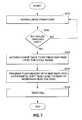
- FIG. 7is a flowchart illustrating a process for shifting a read level based on a number of P/E cycles according to one aspect of the subject technology.
- storage system 100including controller 101 , is in normal drive operation.
- controller 101is configured to monitor the number of P/E cycles experienced by a memory block in flash memory 103 .
- Controller 101may store a number or range of P/E cycles (for example, in storage medium 102 ) for immediate reference during normal drive operation.
- the number or range of P/E cyclesmay be part of software executed by controller 101 .
- step S 702controller 101 determines that the memory block has reached a specific number of P/E cycles (for example, a limit) and/or entered a range of P/E cycles, and, if it has, moves to step S 703 . Otherwise normal drive operations are continued.
- the read level lookup tableis indexed by a range of P/E cycles. Controller 101 , in step S 703 , indexes the lookup table using the current P/E cycle number to obtain the new program verify level based on a range of P/E cycles.
- step S 704controller 101 programs flash memory 103 with the new read level.
- the new read levelis a higher value than the previous value. Thus, the new read level will act in conjunction with the next read operation in step S 705 , effectively shifting 403 the voltage levels used to read the cells in the page and/or block being read to higher values (see FIG. 4 , middle row).
- FIG. 8is a flowchart illustrating a process for shifting a read level based on retention time according to one aspect of the subject technology.
- storage system 100including controller 101 , is in normal drive operation.
- controller 101is configured to monitor the retention time of a memory block in flash memory 103 .
- Controller 101may store a specific retention limit and/or range of retention times (for example, in storage medium 102 ) for immediate reference during normal drive operation.
- the retention limit and/or rangemay be part of software executed by controller 101 .
- controller 101determines whether the memory block has reached a retention time, and, if it has, moves to step S 803 . Otherwise normal drive operations are continued.
- Controller 101accesses a read level lookup table to retrieve a new read level for the retention time.
- the read level lookup tableis indexed by identifiable ranges of retention times. Controller 101 may index the table using the block's retention time to obtain the new read level based on a range of retention times.
- controller 101programs flash memory 103 with the new read level.
- the new read levelis a lower value than the previous value. Thus, the new read level will act in conjunction with the next read operation in step S 805 , effectively shifting 402 the voltage levels used to read the cells in the page and/or block being read to lower values (see FIG. 4 , bottom row).
- the read level adjustment( FIG. 5 or FIG. 6 ) is performed based on retention time and a number of P/E cycles.
- the lookup tablemay provide two levels of indexing. Controller 101 may first index the table using the current P/E cycle number, then perform an additional index to obtain the new read level based on the retention time (or vice versa).
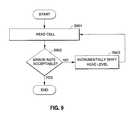
- FIG. 9is a flowchart illustrating a process for iteratively adjusting a read level based on error rate according to one aspect of the subject technology.
- controller 101reads a page and/or block of flash memory 103 (for example, in step S 605 or S 705 ) and a BER is obtained for the read operation.
- controller S 902determines whether the BER is acceptable. Controller 101 may store a specific BER limit (for example, in storage medium 102 ) for immediate reference during normal drive operation.
- the BER limit(and/or range of BER) may be determined by software executed by controller 101 (for example, ECC). If the BER is at an acceptable value, the normal drive operations are continued. If the BER is unacceptable (beyond the BER limit) then, in step S 903 , controller 101 will adjust the read levels by an incremental value prior to attempting to execute a new read operation. In some aspects, controller 101 will determine the incremental value based on stored information from previous read level adjustments and/or recent program verify level adjustments and/or values. For example, if a corresponding program verify level was recently increased (see FIG. 5 ), then controller 101 may choose to increase the read level. However, if an increase in read level is causing excessive BER, then controller may decrease the read level in smaller steps.
- step S 903After the read level has been incremented by step S 903 , the process returns to step S 901 and controller 101 attempts to re-read the page and/or block. The process loops until the BER is reduced to an acceptable value, after which the read operation is completed, data returned, and normal drive operations continue.
- program verify levels and/or read levelsare not fixed apriori.
- theyare dynamically adjusted to conform to flash degradation, and thus moving, voltage threshold distributions as the memory device degrades during cycling and retention.
- theyare dynamically adjusted to reduce bit error rates (BER). For the same level of maximum acceptable BER and the same expected retention time, the subject technology allows one to achieve a higher number of P/E cycles the device can undergo.
- BERbit error rates
- the subject technologyallows the SSD to achieve a lower BER, markedly improving SSD performance throughout the lifetime of the drive.
- the adjustmentoccurs during run-time, for example, when the drive is in operation. It is thus an object of the subject technology to provide the dynamic adjustment herein described to improve SSD performance throughout the lifetime of the drive, and, to allow, for the same level of maximum acceptable BER and the same expected retention time, the device to achieve a higher number of P/E cycles, and, for the same number of P/E cycles and the same expected retention time, achieve a lower BER.
- a processor configured to monitor and control an operation or a componentmay also mean the processor being programmed to monitor and control the operation or the processor being operable to monitor and control the operation.
- a processor configured to execute codecan be construed as a processor programmed to execute code or operable to execute code.
- a phrase such as an “aspect”does not imply that such aspect is essential to the subject technology or that such aspect applies to all configurations of the subject technology.
- a disclosure relating to an aspectmay apply to all configurations, or one or more configurations.
- An aspectmay provide one or more examples.
- a phrase such as an aspectmay refer to one or more aspects and vice versa.
- a phrase such as an “embodiment”does not imply that such embodiment is essential to the subject technology or that such embodiment applies to all configurations of the subject technology.
- a disclosure relating to an embodimentmay apply to all embodiments, or one or more embodiments.
- An embodimentmay provide one or more examples.
- a phrase such as an “embodiment”may refer to one or more embodiments and vice versa.
- a phrase such as a “configuration”does not imply that such configuration is essential to the subject technology or that such configuration applies to all configurations of the subject technology.
- a disclosure relating to a configurationmay apply to all configurations, or one or more configurations.
- a configurationmay provide one or more examples.
- a phrase such as a “configuration”may refer to one or more configurations and vice versa.
Landscapes
- Engineering & Computer Science (AREA)
- Theoretical Computer Science (AREA)
- Computing Systems (AREA)
- Physics & Mathematics (AREA)
- Quality & Reliability (AREA)
- General Engineering & Computer Science (AREA)
- General Physics & Mathematics (AREA)
- Computer Hardware Design (AREA)
- Mathematical Physics (AREA)
- Read Only Memory (AREA)
- Techniques For Improving Reliability Of Storages (AREA)
Abstract
Description
Claims (18)
Priority Applications (1)
| Application Number | Priority Date | Filing Date | Title |
|---|---|---|---|
| US13/044,464US8819503B2 (en) | 2010-07-02 | 2011-03-09 | Apparatus and method for determining an operating condition of a memory cell based on cycle information |
Applications Claiming Priority (2)
| Application Number | Priority Date | Filing Date | Title |
|---|---|---|---|
| US36128810P | 2010-07-02 | 2010-07-02 | |
| US13/044,464US8819503B2 (en) | 2010-07-02 | 2011-03-09 | Apparatus and method for determining an operating condition of a memory cell based on cycle information |
Publications (2)
| Publication Number | Publication Date |
|---|---|
| US20120239991A1 US20120239991A1 (en) | 2012-09-20 |
| US8819503B2true US8819503B2 (en) | 2014-08-26 |
Family
ID=46829460
Family Applications (1)
| Application Number | Title | Priority Date | Filing Date |
|---|---|---|---|
| US13/044,464Active2032-04-03US8819503B2 (en) | 2010-07-02 | 2011-03-09 | Apparatus and method for determining an operating condition of a memory cell based on cycle information |
Country Status (1)
| Country | Link |
|---|---|
| US (1) | US8819503B2 (en) |
Cited By (38)
| Publication number | Priority date | Publication date | Assignee | Title |
|---|---|---|---|---|
| US20130185612A1 (en)* | 2012-01-18 | 2013-07-18 | Samsung Electronics Co., Ltd. | Flash memory system and read method of flash memory system |
| US20130227200A1 (en)* | 2012-02-23 | 2013-08-29 | Stec, Inc. | Determining bias information for offsetting operating variations in memory cells based on wordline address |
| US9047955B2 (en) | 2011-03-30 | 2015-06-02 | Stec, Inc. | Adjusting operating parameters for memory cells based on wordline address and cycle information |
| US20150270008A1 (en)* | 2014-03-21 | 2015-09-24 | Doohyun Kim | Nonvolatile memory device and storage device having the same and operation method thereof |
| US9715908B2 (en)* | 2015-07-01 | 2017-07-25 | Nandext Srl | Controller for a solid-state drive, and related solid-state drive |
| US9778851B2 (en) | 2015-12-03 | 2017-10-03 | Samsung Electronics Co., Ltd. | Method of operation for a nonvolatile memory system and method of operating a memory controller |
| US10095417B1 (en) | 2016-12-13 | 2018-10-09 | EMC IP Holding Company LLC | Method and system for improving flash storage read performance in partially programmed blocks |
| US10289550B1 (en) | 2016-12-30 | 2019-05-14 | EMC IP Holding Company LLC | Method and system for dynamic write-back cache sizing in solid state memory storage |
| US10290331B1 (en) | 2017-04-28 | 2019-05-14 | EMC IP Holding Company LLC | Method and system for modulating read operations to support error correction in solid state memory |
| US10338983B2 (en) | 2016-12-30 | 2019-07-02 | EMC IP Holding Company LLC | Method and system for online program/erase count estimation |
| US10403366B1 (en) | 2017-04-28 | 2019-09-03 | EMC IP Holding Company LLC | Method and system for adapting solid state memory write parameters to satisfy performance goals based on degree of read errors |
| US11069418B1 (en)* | 2016-12-30 | 2021-07-20 | EMC IP Holding Company LLC | Method and system for offline program/erase count estimation |
| US11250926B2 (en) | 2019-10-16 | 2022-02-15 | Sandisk Technologies Llc | Positive feedback and parallel searching enhanced optimal read method for non-volatile memory |
| US11275681B1 (en) | 2017-11-17 | 2022-03-15 | Pure Storage, Inc. | Segmented write requests |
| US11416338B2 (en) | 2020-04-24 | 2022-08-16 | Pure Storage, Inc. | Resiliency scheme to enhance storage performance |
| US11474986B2 (en) | 2020-04-24 | 2022-10-18 | Pure Storage, Inc. | Utilizing machine learning to streamline telemetry processing of storage media |
| US11487455B2 (en) | 2020-12-17 | 2022-11-01 | Pure Storage, Inc. | Dynamic block allocation to optimize storage system performance |
| US11500570B2 (en) | 2018-09-06 | 2022-11-15 | Pure Storage, Inc. | Efficient relocation of data utilizing different programming modes |
| US11507297B2 (en) | 2020-04-15 | 2022-11-22 | Pure Storage, Inc. | Efficient management of optimal read levels for flash storage systems |
| US11513974B2 (en) | 2020-09-08 | 2022-11-29 | Pure Storage, Inc. | Using nonce to control erasure of data blocks of a multi-controller storage system |
| US11520514B2 (en) | 2018-09-06 | 2022-12-06 | Pure Storage, Inc. | Optimized relocation of data based on data characteristics |
| US11581943B2 (en) | 2016-10-04 | 2023-02-14 | Pure Storage, Inc. | Queues reserved for direct access via a user application |
| US11614893B2 (en) | 2010-09-15 | 2023-03-28 | Pure Storage, Inc. | Optimizing storage device access based on latency |
| US11630593B2 (en) | 2021-03-12 | 2023-04-18 | Pure Storage, Inc. | Inline flash memory qualification in a storage system |
| US11681448B2 (en) | 2020-09-08 | 2023-06-20 | Pure Storage, Inc. | Multiple device IDs in a multi-fabric module storage system |
| US11714572B2 (en) | 2019-06-19 | 2023-08-01 | Pure Storage, Inc. | Optimized data resiliency in a modular storage system |
| US11768763B2 (en) | 2020-07-08 | 2023-09-26 | Pure Storage, Inc. | Flash secure erase |
| US11832410B2 (en) | 2021-09-14 | 2023-11-28 | Pure Storage, Inc. | Mechanical energy absorbing bracket apparatus |
| US11947814B2 (en) | 2017-06-11 | 2024-04-02 | Pure Storage, Inc. | Optimizing resiliency group formation stability |
| US11994723B2 (en) | 2021-12-30 | 2024-05-28 | Pure Storage, Inc. | Ribbon cable alignment apparatus |
| US12001684B2 (en) | 2019-12-12 | 2024-06-04 | Pure Storage, Inc. | Optimizing dynamic power loss protection adjustment in a storage system |
| US12001688B2 (en) | 2019-04-29 | 2024-06-04 | Pure Storage, Inc. | Utilizing data views to optimize secure data access in a storage system |
| US12008266B2 (en) | 2010-09-15 | 2024-06-11 | Pure Storage, Inc. | Efficient read by reconstruction |
| US12032848B2 (en) | 2021-06-21 | 2024-07-09 | Pure Storage, Inc. | Intelligent block allocation in a heterogeneous storage system |
| US12039165B2 (en) | 2016-10-04 | 2024-07-16 | Pure Storage, Inc. | Utilizing allocation shares to improve parallelism in a zoned drive storage system |
| US12099742B2 (en) | 2021-03-15 | 2024-09-24 | Pure Storage, Inc. | Utilizing programming page size granularity to optimize data segment storage in a storage system |
| US12153818B2 (en) | 2020-09-24 | 2024-11-26 | Pure Storage, Inc. | Bucket versioning snapshots |
| US12175124B2 (en) | 2018-04-25 | 2024-12-24 | Pure Storage, Inc. | Enhanced data access using composite data views |
Families Citing this family (65)
| Publication number | Priority date | Publication date | Assignee | Title |
|---|---|---|---|---|
| US8819503B2 (en) | 2010-07-02 | 2014-08-26 | Stec, Inc. | Apparatus and method for determining an operating condition of a memory cell based on cycle information |
| US8737141B2 (en)* | 2010-07-07 | 2014-05-27 | Stec, Inc. | Apparatus and method for determining an operating condition of a memory cell based on cycle information |
| US8737136B2 (en) | 2010-07-09 | 2014-05-27 | Stec, Inc. | Apparatus and method for determining a read level of a memory cell based on cycle information |
| US8451662B2 (en)* | 2011-03-03 | 2013-05-28 | Micron Technology, Inc. | Reading memory cell history during program operation for adaptive programming |
| US10481992B1 (en)* | 2011-03-31 | 2019-11-19 | EMC IP Holding Company LLC | Optimization of flash storage |
| JP5404685B2 (en) | 2011-04-06 | 2014-02-05 | 株式会社東芝 | Nonvolatile semiconductor memory device |
| US20130006896A1 (en)* | 2011-06-28 | 2013-01-03 | Seagate Technology Llc | Training Datasets for Memory Devices |
| KR101826140B1 (en)* | 2011-08-04 | 2018-03-22 | 삼성전자주식회사 | Method for operating memory controller, and memory system having the same |
| US10359949B2 (en)* | 2011-10-31 | 2019-07-23 | Apple Inc. | Systems and methods for obtaining and using nonvolatile memory health information |
| US20130145075A1 (en)* | 2011-12-01 | 2013-06-06 | International Business Machines Corporation | Dynamically managing memory lifespan in hybrid storage configurations |
| US20130145077A1 (en)* | 2011-12-01 | 2013-06-06 | International Business Machines Corporation | Dynamically managing memory lifespan in hybrid storage configurations |
| US8832506B2 (en)* | 2012-01-20 | 2014-09-09 | International Business Machines Corporation | Bit error rate based wear leveling for solid state drive memory |
| US20130262942A1 (en)* | 2012-03-27 | 2013-10-03 | Yung-Chiang Chu | Flash memory lifetime evaluation method |
| JP5929456B2 (en)* | 2012-04-17 | 2016-06-08 | ソニー株式会社 | Storage control device, storage device, information processing system, and processing method therefor |
| US9645177B2 (en)* | 2012-05-04 | 2017-05-09 | Seagate Technology Llc | Retention-drift-history-based non-volatile memory read threshold optimization |
| KR102028128B1 (en)* | 2012-08-07 | 2019-10-02 | 삼성전자주식회사 | Operating method of memory system including nonvolatile random access memory and nand flash memory |
| US10230396B1 (en) | 2013-03-05 | 2019-03-12 | Microsemi Solutions (Us), Inc. | Method and apparatus for layer-specific LDPC decoding |
| US9813080B1 (en) | 2013-03-05 | 2017-11-07 | Microsemi Solutions (U.S.), Inc. | Layer specific LDPC decoder |
| US9015409B2 (en)* | 2013-03-15 | 2015-04-21 | Advanced Digital Broadcast Sa | Apparatus and methods for prolonging service life of solid-state memory device in a digital video recorder |
| US9013920B2 (en)* | 2013-04-03 | 2015-04-21 | Western Digital Technologies, Inc. | Systems and methods of write precompensation to extend life of a solid-state memory |
| US9256371B2 (en) | 2013-05-28 | 2016-02-09 | Globalfoundries Inc. | Implementing reinforcement learning based flash control |
| GB201322075D0 (en)* | 2013-12-13 | 2014-01-29 | Ibm | Device for selecting a level for at least one read voltage |
| KR102069274B1 (en) | 2014-02-05 | 2020-01-22 | 삼성전자주식회사 | Memory control method |
| KR102222463B1 (en)* | 2014-03-14 | 2021-03-03 | 삼성전자주식회사 | Storage and timer setting methof and driving methods thereof |
| US9401217B2 (en) | 2014-08-27 | 2016-07-26 | Freescale Semiconductor, Inc. | Flash memory with improved read performance |
| US9799401B2 (en)* | 2014-09-16 | 2017-10-24 | Seagate Technology Llc | Incremental step pulse programming |
| US20160093397A1 (en)* | 2014-09-30 | 2016-03-31 | Emc Corporation | Method and system for improving flash storage utilization using read-threshold tables |
| US10365859B2 (en) | 2014-10-21 | 2019-07-30 | International Business Machines Corporation | Storage array management employing a merged background management process |
| US9563373B2 (en) | 2014-10-21 | 2017-02-07 | International Business Machines Corporation | Detecting error count deviations for non-volatile memory blocks for advanced non-volatile memory block management |
| US9905302B2 (en) | 2014-11-20 | 2018-02-27 | Western Digital Technologies, Inc. | Read level grouping algorithms for increased flash performance |
| US9720754B2 (en) | 2014-11-20 | 2017-08-01 | Western Digital Technologies, Inc. | Read level grouping for increased flash performance |
| US9576671B2 (en) | 2014-11-20 | 2017-02-21 | Western Digital Technologies, Inc. | Calibrating optimal read levels |
| US10339048B2 (en) | 2014-12-23 | 2019-07-02 | International Business Machines Corporation | Endurance enhancement scheme using memory re-evaluation |
| US20160179399A1 (en)* | 2014-12-23 | 2016-06-23 | Sandisk Technologies Inc. | System and Method for Selecting Blocks for Garbage Collection Based on Block Health |
| US9990279B2 (en) | 2014-12-23 | 2018-06-05 | International Business Machines Corporation | Page-level health equalization |
| US9940457B2 (en)* | 2015-02-13 | 2018-04-10 | International Business Machines Corporation | Detecting a cryogenic attack on a memory device with embedded error correction |
| US9606851B2 (en) | 2015-02-02 | 2017-03-28 | International Business Machines Corporation | Error monitoring of a memory device containing embedded error correction |
| US10332613B1 (en) | 2015-05-18 | 2019-06-25 | Microsemi Solutions (Us), Inc. | Nonvolatile memory system with retention monitor |
| US9715430B2 (en)* | 2015-07-01 | 2017-07-25 | Nandext Srl | Controller for a solid-state drive, and related solid-state drive |
| US9799405B1 (en)* | 2015-07-29 | 2017-10-24 | Ip Gem Group, Llc | Nonvolatile memory system with read circuit for performing reads using threshold voltage shift read instruction |
| US9672928B2 (en) | 2015-11-10 | 2017-06-06 | Samsung Electronics Co., Ltd. | Method and apparatus for estimating read levels of nonvolatile memory and for programming pilot signals used for such estimation |
| US20170148525A1 (en)* | 2015-11-25 | 2017-05-25 | Sandisk Technologies Llc | Method and System For Adaptively Adjusting a Verify Voltage to Reduce Storage Raw Bit Error Rate |
| US9886214B2 (en) | 2015-12-11 | 2018-02-06 | Ip Gem Group, Llc | Nonvolatile memory system with erase suspend circuit and method for erase suspend management |
| US9892794B2 (en) | 2016-01-04 | 2018-02-13 | Ip Gem Group, Llc | Method and apparatus with program suspend using test mode |
| US9899092B2 (en) | 2016-01-27 | 2018-02-20 | Ip Gem Group, Llc | Nonvolatile memory system with program step manager and method for program step management |
| US9792998B1 (en) | 2016-03-29 | 2017-10-17 | Sandisk Technologies Llc | System and method for erase detection before programming of a storage device |
| US10157677B2 (en) | 2016-07-28 | 2018-12-18 | Ip Gem Group, Llc | Background reference positioning and local reference positioning using threshold voltage shift read |
| US10291263B2 (en) | 2016-07-28 | 2019-05-14 | Ip Gem Group, Llc | Auto-learning log likelihood ratio |
| US10236915B2 (en) | 2016-07-29 | 2019-03-19 | Microsemi Solutions (U.S.), Inc. | Variable T BCH encoding |
| CN108255634B (en)* | 2016-12-28 | 2020-08-07 | 华为技术有限公司 | Method and device for reading data |
| US10379769B2 (en)* | 2016-12-30 | 2019-08-13 | Western Digital Technologies, Inc. | Continuous adaptive calibration for flash memory devices |
| US10891052B2 (en)* | 2017-06-26 | 2021-01-12 | Western Digital Technologies, Inc. | Adaptive system for optimization of non-volatile storage operational parameters |
| US10777271B2 (en)* | 2017-09-29 | 2020-09-15 | Intel Corporation | Method and apparatus for adjusting demarcation voltages based on cycle count metrics |
| US11184446B2 (en) | 2018-12-05 | 2021-11-23 | Micron Technology, Inc. | Methods and apparatus for incentivizing participation in fog networks |
| US11037637B2 (en)* | 2018-12-10 | 2021-06-15 | Micron Technology, Inc. | Defect detection in memories with time-varying bit error rate |
| US11327551B2 (en)* | 2019-02-14 | 2022-05-10 | Micron Technology, Inc. | Methods and apparatus for characterizing memory devices |
| US11256778B2 (en) | 2019-02-14 | 2022-02-22 | Micron Technology, Inc. | Methods and apparatus for checking the results of characterized memory searches |
| US12118056B2 (en) | 2019-05-03 | 2024-10-15 | Micron Technology, Inc. | Methods and apparatus for performing matrix transformations within a memory array |
| US11481265B2 (en)* | 2019-06-06 | 2022-10-25 | Micron Technology, Inc. | Persistent health monitoring for volatile memory systems |
| US10867655B1 (en) | 2019-07-08 | 2020-12-15 | Micron Technology, Inc. | Methods and apparatus for dynamically adjusting performance of partitioned memory |
| US10971228B2 (en)* | 2019-08-26 | 2021-04-06 | Micron Technology, Inc. | Adaptive application of voltage pulses to stabilize memory cell voltage levels |
| US11449577B2 (en) | 2019-11-20 | 2022-09-20 | Micron Technology, Inc. | Methods and apparatus for performing video processing matrix operations within a memory array |
| US11853385B2 (en) | 2019-12-05 | 2023-12-26 | Micron Technology, Inc. | Methods and apparatus for performing diversity matrix operations within a memory array |
| US12314598B2 (en)* | 2021-03-03 | 2025-05-27 | Gylicon Ltd | Solid state storage device with look-up tables providing improved reference voltages |
| US11687248B2 (en)* | 2021-05-13 | 2023-06-27 | Micron Technology, Inc. | Life time extension of memory device based on rating of individual memory units |
Citations (41)
| Publication number | Priority date | Publication date | Assignee | Title |
|---|---|---|---|---|
| US5729489A (en) | 1995-12-14 | 1998-03-17 | Intel Corporation | Programming flash memory using predictive learning methods |
| US6396742B1 (en) | 2000-07-28 | 2002-05-28 | Silicon Storage Technology, Inc. | Testing of multilevel semiconductor memory |
| US6429785B1 (en)* | 1999-01-08 | 2002-08-06 | Siemens Power Transmission & Distribution Inc. | Revenue meter having precision time clock |
| US20020174394A1 (en)* | 2001-05-16 | 2002-11-21 | Ledford James S. | External control of algorithm execution in a built-in self-test circuit and method therefor |
| US6519184B2 (en) | 2001-04-19 | 2003-02-11 | Hitachi, Ltd. | Non-volatile memory device with plurality of threshold voltage distributions |
| US6643177B1 (en) | 2003-01-21 | 2003-11-04 | Advanced Micro Devices, Inc. | Method for improving read margin in a flash memory device |
| US6675071B1 (en)* | 1999-01-08 | 2004-01-06 | Siemens Transmission & Distribution. Llc | Power quality utility metering system having waveform capture |
| US6888758B1 (en) | 2004-01-21 | 2005-05-03 | Sandisk Corporation | Programming non-volatile memory |
| US20050125199A1 (en)* | 1999-09-23 | 2005-06-09 | Intel Corporation, A California Corporation | Computer system monitoring |
| US20050144358A1 (en)* | 2003-12-30 | 2005-06-30 | Conley Kevin M. | Management of non-volatile memory systems having large erase blocks |
| US6928001B2 (en) | 2000-12-07 | 2005-08-09 | Saifun Semiconductors Ltd. | Programming and erasing methods for a non-volatile memory cell |
| US20050248999A1 (en)* | 2001-08-09 | 2005-11-10 | Renesas Technology Corp. | Memory card and memory controller |
| US20060039196A1 (en)* | 2003-10-03 | 2006-02-23 | Gorobets Sergey A | Corrected data storage and handling methods |
| US7009889B2 (en) | 2004-05-28 | 2006-03-07 | Sandisk Corporation | Comprehensive erase verification for non-volatile memory |
| US20060061795A1 (en)* | 2004-05-27 | 2006-03-23 | Silverbrook Research Pty Ltd | Storage of key in arbitrary locations in memory |
| US7054199B2 (en) | 2004-02-26 | 2006-05-30 | Samsung Electronics Co., Ltd. | Multi level flash memory device and program method |
| US20060244041A1 (en)* | 2005-04-28 | 2006-11-02 | Renesas Technology Corp. | Programmable nonvolatile memory and semiconductor integrated circuit device |
| US20090104900A1 (en)* | 2007-10-22 | 2009-04-23 | Matsushita Electric Industrial Co., Ltd. | Methods and apparatus for controlling the operation of wireless communications systems |
| US20090109756A1 (en) | 2006-03-24 | 2009-04-30 | Micron Technology, Inc. | Memory device with variable trim setting |
| US20090187785A1 (en)* | 2003-10-03 | 2009-07-23 | Gonzalez Carlos J | Flash Memory Data Correction And Scrub Techniques |
| US7599208B2 (en)* | 2006-07-27 | 2009-10-06 | Hynix Semiconductor Inc. | Nonvolatile ferroelectric memory device and refresh method thereof |
| US20090259916A1 (en) | 2008-04-10 | 2009-10-15 | Phison Electronics Corp. | Data accessing method, controller and storage system using the same |
| US7613045B2 (en) | 2007-11-26 | 2009-11-03 | Sandisk Il, Ltd. | Operation sequence and commands for measuring threshold voltage distribution in memory |
| US20090282189A1 (en)* | 2005-08-04 | 2009-11-12 | Best Scott C | Memory controller with refresh logic to accomodate low-retention storage rows in a memory device |
| US20100008137A1 (en) | 2008-07-10 | 2010-01-14 | Chae Kyu Jang | Nonvolatile memory device and program or erase method using the same |
| US7656707B2 (en) | 2007-12-14 | 2010-02-02 | Intel Corporation | Systems and methods for discrete channel decoding of LDPC codes for flash memory |
| US20100110748A1 (en)* | 2007-04-17 | 2010-05-06 | Best Scott C | Hybrid volatile and non-volatile memory device |
| US20100118608A1 (en) | 2008-11-10 | 2010-05-13 | Samsung Electronics Co., Ltd. | Non-volatile memory device, memory card and system, and method determining read voltage in same |
| US20100180073A1 (en) | 2007-12-05 | 2010-07-15 | Hanan Weingarten | Flash memory device with physical cell value deterioration accommodation and methods useful in conjunction therewith |
| US20100315873A1 (en)* | 2009-06-15 | 2010-12-16 | Samsung Electronics Co., Ltd. | Nonvolatile memory device and related programming method |
| US20110167305A1 (en) | 2008-09-30 | 2011-07-07 | Haratsch Erich F | Methods and Apparatus for Soft Data Generation for Memory Devices Based on Performance Factor Adjustment |
| US20110188291A1 (en)* | 2008-07-31 | 2011-08-04 | Unity Semiconductor Corporation | Preservation circuit and methods to maintain values representing data in one or more layers of memory |
| US20110219203A1 (en) | 2008-11-11 | 2011-09-08 | Nokia Corporation | Method and device for temperature-based data refresh in non-volatile memories |
| US8072805B2 (en) | 2009-08-18 | 2011-12-06 | Skymedi Corporation | Method and system of finding a read voltage for a flash memory |
| US20120017138A1 (en)* | 2010-07-13 | 2012-01-19 | Eran Erez | Adaptive Flash Interface |
| US20120239991A1 (en) | 2010-07-02 | 2012-09-20 | Stec, Inc. | Apparatus and method for determining an operating condition of a memory cell based on cycle information |
| US20120236641A1 (en) | 2010-10-05 | 2012-09-20 | STEC, Inc. A California Corporation | Asymmetric log-likelihood ratio for mlc flash channel |
| US8315092B2 (en) | 2010-01-27 | 2012-11-20 | Fusion-Io, Inc. | Apparatus, system, and method for determining a read voltage threshold for solid-state storage media |
| US20120319585A1 (en)* | 2007-09-21 | 2012-12-20 | Point Somee Limited Liability Company | Regulation of Wavelength Shift and Perceived Color of Solid State Lighting with Temperature Variation |
| US20130007344A1 (en)* | 2011-07-01 | 2013-01-03 | Belgal Hanmant P | Apparatus, System, and Method for Refreshing Non-volatile Memory |
| US20130097362A1 (en)* | 2011-10-12 | 2013-04-18 | Phison Electronics Corp. | Data writing method, and memory controller and memory storage apparatus using the same |
- 2011
- 2011-03-09USUS13/044,464patent/US8819503B2/enactiveActive
Patent Citations (48)
| Publication number | Priority date | Publication date | Assignee | Title |
|---|---|---|---|---|
| US5729489A (en) | 1995-12-14 | 1998-03-17 | Intel Corporation | Programming flash memory using predictive learning methods |
| US6675071B1 (en)* | 1999-01-08 | 2004-01-06 | Siemens Transmission & Distribution. Llc | Power quality utility metering system having waveform capture |
| US6429785B1 (en)* | 1999-01-08 | 2002-08-06 | Siemens Power Transmission & Distribution Inc. | Revenue meter having precision time clock |
| US20050125199A1 (en)* | 1999-09-23 | 2005-06-09 | Intel Corporation, A California Corporation | Computer system monitoring |
| US6937521B2 (en) | 2000-05-04 | 2005-08-30 | Saifun Semiconductors Ltd. | Programming and erasing methods for a non-volatile memory cell |
| US6396742B1 (en) | 2000-07-28 | 2002-05-28 | Silicon Storage Technology, Inc. | Testing of multilevel semiconductor memory |
| US6928001B2 (en) | 2000-12-07 | 2005-08-09 | Saifun Semiconductors Ltd. | Programming and erasing methods for a non-volatile memory cell |
| US6519184B2 (en) | 2001-04-19 | 2003-02-11 | Hitachi, Ltd. | Non-volatile memory device with plurality of threshold voltage distributions |
| US20020174394A1 (en)* | 2001-05-16 | 2002-11-21 | Ledford James S. | External control of algorithm execution in a built-in self-test circuit and method therefor |
| US20080229164A1 (en)* | 2001-08-09 | 2008-09-18 | Renesas Technology Corp. | Memory card and memory controller |
| US20050248999A1 (en)* | 2001-08-09 | 2005-11-10 | Renesas Technology Corp. | Memory card and memory controller |
| US6643177B1 (en) | 2003-01-21 | 2003-11-04 | Advanced Micro Devices, Inc. | Method for improving read margin in a flash memory device |
| US20090187785A1 (en)* | 2003-10-03 | 2009-07-23 | Gonzalez Carlos J | Flash Memory Data Correction And Scrub Techniques |
| US20110055468A1 (en)* | 2003-10-03 | 2011-03-03 | Gonzalez Carlos J | Flash Memory Data Correction and Scrub Techniques |
| US20060039196A1 (en)* | 2003-10-03 | 2006-02-23 | Gorobets Sergey A | Corrected data storage and handling methods |
| US7173852B2 (en)* | 2003-10-03 | 2007-02-06 | Sandisk Corporation | Corrected data storage and handling methods |
| US20050144358A1 (en)* | 2003-12-30 | 2005-06-30 | Conley Kevin M. | Management of non-volatile memory systems having large erase blocks |
| US6888758B1 (en) | 2004-01-21 | 2005-05-03 | Sandisk Corporation | Programming non-volatile memory |
| US7054199B2 (en) | 2004-02-26 | 2006-05-30 | Samsung Electronics Co., Ltd. | Multi level flash memory device and program method |
| US20060061795A1 (en)* | 2004-05-27 | 2006-03-23 | Silverbrook Research Pty Ltd | Storage of key in arbitrary locations in memory |
| US7009889B2 (en) | 2004-05-28 | 2006-03-07 | Sandisk Corporation | Comprehensive erase verification for non-volatile memory |
| US20060244041A1 (en)* | 2005-04-28 | 2006-11-02 | Renesas Technology Corp. | Programmable nonvolatile memory and semiconductor integrated circuit device |
| US7812389B2 (en)* | 2005-04-28 | 2010-10-12 | Renesas Technology Corp. | Programmable nonvolatile memory and semiconductor integrated circuit device |
| US20090282189A1 (en)* | 2005-08-04 | 2009-11-12 | Best Scott C | Memory controller with refresh logic to accomodate low-retention storage rows in a memory device |
| US20090109756A1 (en) | 2006-03-24 | 2009-04-30 | Micron Technology, Inc. | Memory device with variable trim setting |
| US7599208B2 (en)* | 2006-07-27 | 2009-10-06 | Hynix Semiconductor Inc. | Nonvolatile ferroelectric memory device and refresh method thereof |
| US20100110748A1 (en)* | 2007-04-17 | 2010-05-06 | Best Scott C | Hybrid volatile and non-volatile memory device |
| US20120319585A1 (en)* | 2007-09-21 | 2012-12-20 | Point Somee Limited Liability Company | Regulation of Wavelength Shift and Perceived Color of Solid State Lighting with Temperature Variation |
| US20090104900A1 (en)* | 2007-10-22 | 2009-04-23 | Matsushita Electric Industrial Co., Ltd. | Methods and apparatus for controlling the operation of wireless communications systems |
| US8086225B2 (en)* | 2007-10-22 | 2011-12-27 | Panasonic Corporation | Methods and apparatus for controlling the operation of wireless communications systems |
| US7613045B2 (en) | 2007-11-26 | 2009-11-03 | Sandisk Il, Ltd. | Operation sequence and commands for measuring threshold voltage distribution in memory |
| US20100180073A1 (en) | 2007-12-05 | 2010-07-15 | Hanan Weingarten | Flash memory device with physical cell value deterioration accommodation and methods useful in conjunction therewith |
| US7656707B2 (en) | 2007-12-14 | 2010-02-02 | Intel Corporation | Systems and methods for discrete channel decoding of LDPC codes for flash memory |
| US20090259916A1 (en) | 2008-04-10 | 2009-10-15 | Phison Electronics Corp. | Data accessing method, controller and storage system using the same |
| US20100008137A1 (en) | 2008-07-10 | 2010-01-14 | Chae Kyu Jang | Nonvolatile memory device and program or erase method using the same |
| US20110188291A1 (en)* | 2008-07-31 | 2011-08-04 | Unity Semiconductor Corporation | Preservation circuit and methods to maintain values representing data in one or more layers of memory |
| US20120147660A1 (en)* | 2008-07-31 | 2012-06-14 | Unity Semiconductor Corporation | Preservation Circuit And Methods To Maintain Values Representing Data In One Or More Layers Of Memory |
| US20110167305A1 (en) | 2008-09-30 | 2011-07-07 | Haratsch Erich F | Methods and Apparatus for Soft Data Generation for Memory Devices Based on Performance Factor Adjustment |
| US20100118608A1 (en) | 2008-11-10 | 2010-05-13 | Samsung Electronics Co., Ltd. | Non-volatile memory device, memory card and system, and method determining read voltage in same |
| US20110219203A1 (en) | 2008-11-11 | 2011-09-08 | Nokia Corporation | Method and device for temperature-based data refresh in non-volatile memories |
| US20100315873A1 (en)* | 2009-06-15 | 2010-12-16 | Samsung Electronics Co., Ltd. | Nonvolatile memory device and related programming method |
| US8072805B2 (en) | 2009-08-18 | 2011-12-06 | Skymedi Corporation | Method and system of finding a read voltage for a flash memory |
| US8315092B2 (en) | 2010-01-27 | 2012-11-20 | Fusion-Io, Inc. | Apparatus, system, and method for determining a read voltage threshold for solid-state storage media |
| US20120239991A1 (en) | 2010-07-02 | 2012-09-20 | Stec, Inc. | Apparatus and method for determining an operating condition of a memory cell based on cycle information |
| US20120017138A1 (en)* | 2010-07-13 | 2012-01-19 | Eran Erez | Adaptive Flash Interface |
| US20120236641A1 (en) | 2010-10-05 | 2012-09-20 | STEC, Inc. A California Corporation | Asymmetric log-likelihood ratio for mlc flash channel |
| US20130007344A1 (en)* | 2011-07-01 | 2013-01-03 | Belgal Hanmant P | Apparatus, System, and Method for Refreshing Non-volatile Memory |
| US20130097362A1 (en)* | 2011-10-12 | 2013-04-18 | Phison Electronics Corp. | Data writing method, and memory controller and memory storage apparatus using the same |
Non-Patent Citations (3)
| Title |
|---|
| Hongchao Zhou; Anxiao Jiang; Bruck, J., "Error-correcting schemes with dynamic thresholds in nonvolatile memories," Information Theory Proceedings (ISIT), 2011 IEEE International Symposium on , vol., no., pp. 2143,2147, Jul. 31, 2011-Aug. 5, 2011.* |
| Shih-Liang Chen; Bo-Ru Ke; Jian-Nan Chen; Chih-Tsun Huang, "Reliability analysis and improvement for multi-level non-volatile memories with soft information," Design Automation Conference (DAC), 2011 48th ACM/EDAC/IEEE , vol., no., pp. 753,758, Jun. 5-9, 2011.* |
| Yu Cai; Yalcin, G.; Mutlu, O.; Haratsch, E.F.; Cristal, A.; Unsal, O.S.; Ken Mai, "Flash correct-and-refresh: Retention-aware error management for increased flash memory lifetime," Computer Design (ICCD), 2012 IEEE 30th International Conference on , vol., no., pp. 94,101, Sep. 30, 2012-Oct. 3, 2012.* |
Cited By (45)
| Publication number | Priority date | Publication date | Assignee | Title |
|---|---|---|---|---|
| US12008266B2 (en) | 2010-09-15 | 2024-06-11 | Pure Storage, Inc. | Efficient read by reconstruction |
| US11614893B2 (en) | 2010-09-15 | 2023-03-28 | Pure Storage, Inc. | Optimizing storage device access based on latency |
| US12282686B2 (en) | 2010-09-15 | 2025-04-22 | Pure Storage, Inc. | Performing low latency operations using a distinct set of resources |
| US9047955B2 (en) | 2011-03-30 | 2015-06-02 | Stec, Inc. | Adjusting operating parameters for memory cells based on wordline address and cycle information |
| US9224456B2 (en) | 2011-03-30 | 2015-12-29 | Hgst Technologies Santa Ana, Inc. | Setting operating parameters for memory cells based on wordline address and cycle information |
| US20130185612A1 (en)* | 2012-01-18 | 2013-07-18 | Samsung Electronics Co., Ltd. | Flash memory system and read method of flash memory system |
| US20130227200A1 (en)* | 2012-02-23 | 2013-08-29 | Stec, Inc. | Determining bias information for offsetting operating variations in memory cells based on wordline address |
| US9195586B2 (en)* | 2012-02-23 | 2015-11-24 | Hgst Technologies Santa Ana, Inc. | Determining bias information for offsetting operating variations in memory cells based on wordline address |
| US9377962B2 (en)* | 2012-02-23 | 2016-06-28 | Hgst Technologies Santa Ana, Inc. | Determining bias information for offsetting operating variations in memory cells |
| US20150270008A1 (en)* | 2014-03-21 | 2015-09-24 | Doohyun Kim | Nonvolatile memory device and storage device having the same and operation method thereof |
| US9864682B2 (en)* | 2014-03-21 | 2018-01-09 | Samsung Electronics Co., Ltd. | Nonvolatile memory device and storage device having the same and operation method thereof |
| US9715908B2 (en)* | 2015-07-01 | 2017-07-25 | Nandext Srl | Controller for a solid-state drive, and related solid-state drive |
| US10089016B2 (en) | 2015-12-03 | 2018-10-02 | Samsung Electronics Co., Ltd. | Method of operation for a nonvolatile memory system and method of operating a memory controller |
| US9778851B2 (en) | 2015-12-03 | 2017-10-03 | Samsung Electronics Co., Ltd. | Method of operation for a nonvolatile memory system and method of operating a memory controller |
| US11581943B2 (en) | 2016-10-04 | 2023-02-14 | Pure Storage, Inc. | Queues reserved for direct access via a user application |
| US12039165B2 (en) | 2016-10-04 | 2024-07-16 | Pure Storage, Inc. | Utilizing allocation shares to improve parallelism in a zoned drive storage system |
| US10095417B1 (en) | 2016-12-13 | 2018-10-09 | EMC IP Holding Company LLC | Method and system for improving flash storage read performance in partially programmed blocks |
| US11069418B1 (en)* | 2016-12-30 | 2021-07-20 | EMC IP Holding Company LLC | Method and system for offline program/erase count estimation |
| US10338983B2 (en) | 2016-12-30 | 2019-07-02 | EMC IP Holding Company LLC | Method and system for online program/erase count estimation |
| US10289550B1 (en) | 2016-12-30 | 2019-05-14 | EMC IP Holding Company LLC | Method and system for dynamic write-back cache sizing in solid state memory storage |
| US10861556B2 (en) | 2017-04-28 | 2020-12-08 | EMC IP Holding Company LLC | Method and system for adapting solid state memory write parameters to satisfy performance goals based on degree of read errors |
| US10403366B1 (en) | 2017-04-28 | 2019-09-03 | EMC IP Holding Company LLC | Method and system for adapting solid state memory write parameters to satisfy performance goals based on degree of read errors |
| US10290331B1 (en) | 2017-04-28 | 2019-05-14 | EMC IP Holding Company LLC | Method and system for modulating read operations to support error correction in solid state memory |
| US11947814B2 (en) | 2017-06-11 | 2024-04-02 | Pure Storage, Inc. | Optimizing resiliency group formation stability |
| US11275681B1 (en) | 2017-11-17 | 2022-03-15 | Pure Storage, Inc. | Segmented write requests |
| US12175124B2 (en) | 2018-04-25 | 2024-12-24 | Pure Storage, Inc. | Enhanced data access using composite data views |
| US11500570B2 (en) | 2018-09-06 | 2022-11-15 | Pure Storage, Inc. | Efficient relocation of data utilizing different programming modes |
| US11520514B2 (en) | 2018-09-06 | 2022-12-06 | Pure Storage, Inc. | Optimized relocation of data based on data characteristics |
| US12001688B2 (en) | 2019-04-29 | 2024-06-04 | Pure Storage, Inc. | Utilizing data views to optimize secure data access in a storage system |
| US11714572B2 (en) | 2019-06-19 | 2023-08-01 | Pure Storage, Inc. | Optimized data resiliency in a modular storage system |
| US11250926B2 (en) | 2019-10-16 | 2022-02-15 | Sandisk Technologies Llc | Positive feedback and parallel searching enhanced optimal read method for non-volatile memory |
| US12001684B2 (en) | 2019-12-12 | 2024-06-04 | Pure Storage, Inc. | Optimizing dynamic power loss protection adjustment in a storage system |
| US11507297B2 (en) | 2020-04-15 | 2022-11-22 | Pure Storage, Inc. | Efficient management of optimal read levels for flash storage systems |
| US11474986B2 (en) | 2020-04-24 | 2022-10-18 | Pure Storage, Inc. | Utilizing machine learning to streamline telemetry processing of storage media |
| US11416338B2 (en) | 2020-04-24 | 2022-08-16 | Pure Storage, Inc. | Resiliency scheme to enhance storage performance |
| US11768763B2 (en) | 2020-07-08 | 2023-09-26 | Pure Storage, Inc. | Flash secure erase |
| US11681448B2 (en) | 2020-09-08 | 2023-06-20 | Pure Storage, Inc. | Multiple device IDs in a multi-fabric module storage system |
| US11513974B2 (en) | 2020-09-08 | 2022-11-29 | Pure Storage, Inc. | Using nonce to control erasure of data blocks of a multi-controller storage system |
| US12153818B2 (en) | 2020-09-24 | 2024-11-26 | Pure Storage, Inc. | Bucket versioning snapshots |
| US11487455B2 (en) | 2020-12-17 | 2022-11-01 | Pure Storage, Inc. | Dynamic block allocation to optimize storage system performance |
| US11630593B2 (en) | 2021-03-12 | 2023-04-18 | Pure Storage, Inc. | Inline flash memory qualification in a storage system |
| US12099742B2 (en) | 2021-03-15 | 2024-09-24 | Pure Storage, Inc. | Utilizing programming page size granularity to optimize data segment storage in a storage system |
| US12032848B2 (en) | 2021-06-21 | 2024-07-09 | Pure Storage, Inc. | Intelligent block allocation in a heterogeneous storage system |
| US11832410B2 (en) | 2021-09-14 | 2023-11-28 | Pure Storage, Inc. | Mechanical energy absorbing bracket apparatus |
| US11994723B2 (en) | 2021-12-30 | 2024-05-28 | Pure Storage, Inc. | Ribbon cable alignment apparatus |
Also Published As
| Publication number | Publication date |
|---|---|
| US20120239991A1 (en) | 2012-09-20 |
Similar Documents
| Publication | Publication Date | Title |
|---|---|---|
| US8819503B2 (en) | Apparatus and method for determining an operating condition of a memory cell based on cycle information | |
| US10613781B2 (en) | Apparatus and method for determining an operating condition of a memory cell based on cycle information | |
| US9377962B2 (en) | Determining bias information for offsetting operating variations in memory cells | |
| US9224456B2 (en) | Setting operating parameters for memory cells based on wordline address and cycle information | |
| US8364888B2 (en) | Erase-suspend system and method | |
| US8737136B2 (en) | Apparatus and method for determining a read level of a memory cell based on cycle information | |
| US8694715B2 (en) | Methods for adaptively programming flash memory devices and flash memory systems incorporating same | |
| US8484519B2 (en) | Optimal programming levels for LDPC | |
| US9305640B2 (en) | Asymmetric log-likelihood ratio for flash channel | |
| US9905302B2 (en) | Read level grouping algorithms for increased flash performance | |
| CN102667944B (en) | Non-volatile memory and method for managing errors through read-after-write and adaptive rewrite | |
| US10580485B2 (en) | System and method for adjusting read levels in a storage device based on bias functions | |
| US20140359202A1 (en) | Reading voltage calculation in solid-state storage devices | |
| US20100110798A1 (en) | Program window adjust for memory cell signal line delay | |
| US9983991B2 (en) | Data storage based on rank modulation in single-level flash memory | |
| WO2009053963A2 (en) | Methods for adaptively programming flash memory devices and flash memory systems incorporating same | |
| WO2008093327A1 (en) | Flash memory with improved programming precision | |
| US10008275B1 (en) | Control method for solid state storage device | |
| US8605501B2 (en) | System and method for determining data dependent noise calculation for a flash channel | |
| CN112562772B (en) | Adaptive low density parity check hard decoder | |
| KR20090110648A (en) | How to write data to flash memory, how to read data recorded in flash memory, and flash memory system |
Legal Events
| Date | Code | Title | Description |
|---|---|---|---|
| AS | Assignment | Owner name:STEC, INC., CALIFORNIA Free format text:ASSIGNMENT OF ASSIGNORS INTEREST;ASSIGNOR:MELIK-MARTIROSIAN, ASHOT;REEL/FRAME:025936/0627 Effective date:20110221 | |
| SULP | Surcharge for late payment | ||
| STCF | Information on status: patent grant | Free format text:PATENTED CASE | |
| AS | Assignment | Owner name:HGST TECHNOLOGIES SANTA ANA, INC., CALIFORNIA Free format text:CHANGE OF NAME;ASSIGNOR:STEC, INC.;REEL/FRAME:036042/0390 Effective date:20131105 | |
| MAFP | Maintenance fee payment | Free format text:PAYMENT OF MAINTENANCE FEE, 4TH YEAR, LARGE ENTITY (ORIGINAL EVENT CODE: M1551) Year of fee payment:4 | |
| AS | Assignment | Owner name:WESTERN DIGITAL TECHNOLOGIES, INC., CALIFORNIA Free format text:ASSIGNMENT OF ASSIGNORS INTEREST;ASSIGNOR:HGST TECHNOLOGIES SANTA ANA, INC.;REEL/FRAME:046174/0446 Effective date:20180410 | |
| AS | Assignment | Owner name:JPMORGAN CHASE BANK, N.A., AS AGENT, ILLINOIS Free format text:SECURITY INTEREST;ASSIGNOR:WESTERN DIGITAL TECHNOLOGIES, INC.;REEL/FRAME:052915/0566 Effective date:20200113 | |
| MAFP | Maintenance fee payment | Free format text:PAYMENT OF MAINTENANCE FEE, 8TH YEAR, LARGE ENTITY (ORIGINAL EVENT CODE: M1552); ENTITY STATUS OF PATENT OWNER: LARGE ENTITY Year of fee payment:8 | |
| AS | Assignment | Owner name:WESTERN DIGITAL TECHNOLOGIES, INC., CALIFORNIA Free format text:RELEASE OF SECURITY INTEREST AT REEL 052915 FRAME 0566;ASSIGNOR:JPMORGAN CHASE BANK, N.A.;REEL/FRAME:059127/0001 Effective date:20220203 | |
| AS | Assignment | Owner name:JPMORGAN CHASE BANK, N.A., ILLINOIS Free format text:PATENT COLLATERAL AGREEMENT - A&R LOAN AGREEMENT;ASSIGNOR:WESTERN DIGITAL TECHNOLOGIES, INC.;REEL/FRAME:064715/0001 Effective date:20230818 Owner name:JPMORGAN CHASE BANK, N.A., ILLINOIS Free format text:PATENT COLLATERAL AGREEMENT - DDTL LOAN AGREEMENT;ASSIGNOR:WESTERN DIGITAL TECHNOLOGIES, INC.;REEL/FRAME:067045/0156 Effective date:20230818 | |
| AS | Assignment | Owner name:SANDISK TECHNOLOGIES, INC., CALIFORNIA Free format text:ASSIGNMENT OF ASSIGNORS INTEREST;ASSIGNOR:WESTERN DIGITAL TECHNOLOGIES, INC.;REEL/FRAME:067567/0682 Effective date:20240503 | |
| AS | Assignment | Owner name:SANDISK TECHNOLOGIES, INC., CALIFORNIA Free format text:CHANGE OF NAME;ASSIGNOR:SANDISK TECHNOLOGIES, INC.;REEL/FRAME:067982/0032 Effective date:20240621 | |
| AS | Assignment | Owner name:JPMORGAN CHASE BANK, N.A., AS THE AGENT, ILLINOIS Free format text:PATENT COLLATERAL AGREEMENT;ASSIGNOR:SANDISK TECHNOLOGIES, INC.;REEL/FRAME:068762/0494 Effective date:20240820 | |
| AS | Assignment | Owner name:WESTERN DIGITAL TECHNOLOGIES, INC., CALIFORNIA Free format text:ASSIGNMENT OF ASSIGNORS INTEREST;ASSIGNOR:SANDISK TECHNOLOGIES, INC.;REEL/FRAME:069168/0273 Effective date:20241008 | |
| AS | Assignment | Owner name:JPMORGAN CHASE BANK, N.A., AS COLLATERAL AGENT, ILLINOIS Free format text:SECURITY AGREEMENT (SUPPLEMENTAL);ASSIGNOR:WESTERN DIGITAL TECHNOLOGIES, INC.;REEL/FRAME:069411/0208 Effective date:20241030 |