US8816754B1 - Body bias circuits and methods - Google Patents
Body bias circuits and methodsDownload PDFInfo
- Publication number
- US8816754B1 US8816754B1US13/668,063US201213668063AUS8816754B1US 8816754 B1US8816754 B1US 8816754B1US 201213668063 AUS201213668063 AUS 201213668063AUS 8816754 B1US8816754 B1US 8816754B1
- Authority
- US
- United States
- Prior art keywords
- monitor
- circuit
- tut
- section
- power supply
- Prior art date
- Legal status (The legal status is an assumption and is not a legal conclusion. Google has not performed a legal analysis and makes no representation as to the accuracy of the status listed.)
- Active
Links
Images


Classifications
- H—ELECTRICITY
- H03—ELECTRONIC CIRCUITRY
- H03K—PULSE TECHNIQUE
- H03K17/00—Electronic switching or gating, i.e. not by contact-making and –breaking
- H03K17/14—Modifications for compensating variations of physical values, e.g. of temperature
- H03K17/145—Modifications for compensating variations of physical values, e.g. of temperature in field-effect transistor switches
- H—ELECTRICITY
- H03—ELECTRONIC CIRCUITRY
- H03K—PULSE TECHNIQUE
- H03K19/00—Logic circuits, i.e. having at least two inputs acting on one output; Inverting circuits
- H03K19/003—Modifications for increasing the reliability for protection
- H03K19/00369—Modifications for compensating variations of temperature, supply voltage or other physical parameters
- H03K19/00384—Modifications for compensating variations of temperature, supply voltage or other physical parameters in field effect transistor circuits
- H—ELECTRICITY
- H10—SEMICONDUCTOR DEVICES; ELECTRIC SOLID-STATE DEVICES NOT OTHERWISE PROVIDED FOR
- H10D—INORGANIC ELECTRIC SEMICONDUCTOR DEVICES
- H10D30/00—Field-effect transistors [FET]
- H10D30/60—Insulated-gate field-effect transistors [IGFET]
- H10D30/62—Fin field-effect transistors [FinFET]
- H10D30/6211—Fin field-effect transistors [FinFET] having fin-shaped semiconductor bodies integral with the bulk semiconductor substrates
Definitions
- the present inventionrelates generally to integrated circuit (IC) devices, and more particularly to body bias circuits and methods for insulated gate field effect transistors of IC devices.
- ICintegrated circuit
- Integrated circuit (IC) devicescan be subject to manufacturing variations that can impact performance.
- electrical signalscan be transmitted via an interconnect structure formed by multiple metallization layers, separated from one another by interlayer dielectrics (ILDs).
- ILDsinterlayer dielectrics
- Signalscan be generated by transistors driving metallization layers between different potentials.
- CMPchemical-mechanical polishing
- Active devicesmay also be subject to some variation in performance.
- uncontrollable manufacturing variationscan result in “fast” transistors and “slow” transistors.
- Fast transistorscan provide faster driving capability than slow transistors.
- Such fast vs. slow variationscan be systematic, i.e., they can affect the mean value of performance parameters.
- timing pathscan be designed with sufficient margin to be adequate for a slowest case. This can require large signal driving devices and increased power consumption, as well as increased design effort. For some very high performance IC devices, such variations can present a limit to device speed and/or reliability.
- FIG. 1is a block schematic diagram of an integrated circuit device according to an embodiment.
- FIG. 2is a block schematic diagram of a combination logic section according to an embodiment.
- FIG. 3is a block schematic diagram of a monitoring section that can be included in embodiments.
- FIGS. 4A and 4Bare diagrams showing a monitoring section and operation that can be included in embodiments.
- FIG. 5is a block schematic diagram of another monitoring section that can be included in embodiments.
- FIG. 6Ais a block schematic diagram of a transistor under test (TUT) selection circuit that can be included in embodiments.
- FIG. 6Bis a block schematic diagram of a load capacitance selection circuit that can be included in embodiments.
- FIG. 7is a block schematic diagram of a drive monitor circuit according to another embodiment.
- FIG. 8is a diagram of a metal-metal capacitor that can be included in embodiments.
- FIG. 9is a diagram showing capacitance corresponding to metallization fabrication variations.
- FIG. 10is a block schematic diagram of an integrated circuit device according to an embodiment.
- FIG. 11is a block schematic diagram of a power gating circuit according to an embodiment.
- FIG. 12is a block schematic diagram of a core biasing circuit that can be used in an embodiment like that of FIG. 11 .
- FIG. 13is a block schematic diagram of a regulator circuit according to an embodiment.
- FIGS. 14A to 14Dare side cross sectional views of devices that can be body biased according to embodiments.
- FIG. 15Ais a side cross sectional view of a deeply depleted channel (DDC) transistor that can be included in embodiments.
- DDCdeeply depleted channel
- FIG. 15Bis a side cross sectional view of FinFET transistor that can be included in embodiments.
- FIG. 15Cis a side cross sectional views of FinFET transistor having a screening region, and optionally, a threshold voltage set region, that can be included in embodiments.
- FIGS. 16A-0 to 16 B- 1are graphs showing how transistor performance can be measured with a circuit like that of FIG. 4A , and how a body bias can be adjusted to change transistor performance.
- FIG. 17shows one embodiment of a bias voltage distribution network using monitor circuits to implement a fine grained body biasing technique.
- FIG. 18shows one embodiment of the bias tuning circuit using a resistive divider to generate the local body bias voltage.
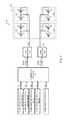
- FIG. 1is a block schematic diagram of an integrated circuit (IC) device 100 according to one embodiment.
- An IC device 100can include a number of monitoring sections 102 - 0 to - n , a combination logic section 104 , an n-type body bias circuit 106 - 0 , a p-type body bias circuit 106 - 1 , and an operational section 150 .
- Monitoring sections ( 102 - 0 to - n )can include physical structures corresponding to those of the IC device 100 .
- Each monitoring section ( 102 - 0 to - n )can include physical circuit elements of the IC device 100 that can vary according to process variation. Monitoring sections ( 102 - 0 to - n ) can output monitor values M0 to Mn that reflect variations in performance resulting from variations in process. In particular embodiments, each monitoring section ( 102 - 0 to - n ) can provide a monitor value (M0 to Mn) that is dominated by one or more particular process features. In the particular embodiment shown, monitor sections ( 102 - 0 to - n ) include those dominated by: n-type transistor performance, p-type transistor performance, wiring, and diffusion. It is understood that such features are but exemplary.
- a monitoring sectioncan include a ring oscillator circuit having an oscillating frequency reflecting the effect of one or more sources of process variations.
- a monitoring sectioncan include a transistor drive monitoring section, embodiments of which are described in more detail below.
- Monitor sections ( 102 - 0 to - n )can provide monitor values in various ways. For example, in some embodiments or modes of operation, monitor sections ( 102 - 0 to - n ) can be operational during a test or characterization phase. Monitor values (M0 to Mn) generated in the test/characterization phase can be stored such that they remain fixed throughout the operation of the device. After the monitor values have been generated, the combination logic section 104 can access the stored monitor values to set the n-type and p-type transistor body bias voltages based on one or more of the stored monitor values during the operation of the device. The monitor values can be stored in internal storage that is part of the combination logic section 104 , or in external storage that is located outside the combination logic section 104 and accessed by the combination logic section 104 .
- monitor sections( 102 - 0 to - n ) can be activated periodically and/or constantly, allowing monitor values to be updated while the device is in operation.
- a combination logic section 104can receive the periodically or continuously updated monitor values ( 102 - 0 to - n ) and modify the n-type and p-type body bias voltages based on the updated monitor values.
- monitor sections ( 102 - 0 to - n )can be enabled in response to a command input to the IC device 100 , where the monitor sections generate and store updated monitor values during a test/characterization phase that is initiated in response to receiving the command input at the IC device.
- the monitor sections ( 102 - 0 to - n )can be enabled in response to received status information indicative of particular conditions or changes to particular conditions (e.g., power-on, reset, temperature, power supply voltage, etc.).
- test/characterization phasecan be initiated if temperature exceeds a predetermined threshold value, such that monitor sections ( 102 - 0 to - n ) are enabled to generate and store updated monitor values that are used to modify the n-type and p-type body bias voltages.
- a combination logic section 104can receive monitor values (M0 to Mn), and from such values, generates n-type and p-type body bias control values (NBias, PBias).
- a combination logic section 104can assign different weights to one or more of the monitor values (M0 to Mn) such that particular monitor values (M0 to Mn) have a greater weight over others, to reflect how one type of process variation can have a greater effect than other types of process variations on a particular performance characteristic of a circuit within the IC device 100 . In this way, body biases can be tuned to optimize an IC device for a particular performance target.
- bias control valuescan be static during the operation of the IC device 100 .
- such valuescan be static, changing according to mode of operation, and/or operating conditions.
- the weightscan compensate for differing sensitivities of the monitoring circuits to the variations, as well as the IC's sensitivity to such variations.
- bias control values (NBias, PBias) generated by a combination logic section 104can be digital or analog values.
- An n-type body bias circuit 106 - 0can receive a bias control value (NBias), and in response generate an n-channel transistor body bias voltage (Vbn). That is, a voltage Vbn can vary according to the bias control value NBias. In very particular embodiments, Vbn can vary from a “back bias” level (VBB) to a forward bias level (VFB). A back bias level can force a body region below a low power supply voltage (e.g., less than VSS) to increase a threshold voltage, but lower a switching speed of an n-type transistor (as compared to such a transistor having a body bias of VSS).
- a low power supply voltagee.g., less than VSS
- a forward bias levelcan force a body region above a low power supply voltage (e.g., greater than VSS) to lower a threshold voltage of a transistor, but increase a switching speed of an n-type transistor (as compared to such a transistor having a body bias of VSS).
- a low power supply voltagee.g., greater than VSS
- a p-type body bias circuit 106 - 1can receive a bias control value (PBias), and in response, generate a p-channel transistor body bias voltage (Vbp).
- Vbpcan vary from a “back bias” level (e.g., greater than a high power supply voltage VDD) to a “forward bias” level (e.g., less than VDD).
- An operational section 150can include transistors formed with body regions that can receive the body bias voltages (Vbn, Vbp). Such transistors can be arranged to provide a predetermined function as part of different functional blocks having different predetermined target performance characteristics, where the performance of each functional block can be independently adjusted by selection of the n-type and p-type body bias voltages. Accordingly, an operational section 150 can include n-type transistors formed in p-type body regions 108 - 0 , and p-type transistors formed in n-type body regions 108 - 1 . Body regions ( 108 - 0 / 1 ) can vary according to transistor type. Various examples of transistors that can have a body bias will be described in more detail below.
- Body bias voltagescan be applied to transistors of operational section 150 to compensate for process variations detected by monitoring sections ( 102 - 0 to - n ).
- a body bias voltagecan be lowered, to increase the driving speed of the transistors in the device.
- a body bias voltagecan be reduced or increased, for p-type and n-type transistors respectively, to bring the performance of the transistors back into a desired speed range.
- the opposite type of adjustmentis possible as well. If metallization presents a smaller capacitance or transistors are “fast”, a body bias can be increased or decreased to compensate for these variations by corresponding changes of the transistor speeds in response to the applied body bias.
- FIG. 2shows a combination logic section 204 according to an embodiment.
- a combination logic section 204can be one implementation of that shown as 104 in FIG. 1 .
- a combination logic section 204can include a monitor value store 210 , weight value store 212 , and a body bias value generator circuit 214 .
- a monitor value store 210can store monitor values (Mo to Mn) received from monitor sections (not shown). As noted above, monitor values can be static or dynamic.
- a monitor value store 210can be formed with any suitable storage elements, including non-volatile elements, volatile storage elements, or combinations of thereof.
- a weight value store 212can provide weight values (W0 to Wi) to increase or decrease the effect that a monitor value can have on a resulting bias control value (PBias, NBias), typically achieved by multiplying the monitor value by the corresponding weight value.
- weight values (W0 to Wi)can be determined through simulation or characterization of circuits within an integrated circuit device.
- weight values (W0 to Wi)can be established by testing integrated devices of a same manufacturing group (e.g., lot), or by circuits on the device itself (such as monitor sections, described herein). Once such weight values are determined, the values (W0 to Wn) can remain fixed during the operation of the device, or alternatively, can be updated during the operation of the device.
- a monitor value store 210can be formed with any suitable storage elements, including non-volatile elements, volatile storage elements (e.g., flash memory, fuses, SRAM, latches), or combinations of thereof.
- volatile storage elementse.g., flash memory, fuses, SRAM, latches
- a back end processsuch as the opening of fusible links can be used to set the weight values.
- a bias value generator circuit 214can apply weighting values (W0 to Wn) to corresponding monitor values (M0 to Mn), and combine the results to generate bias control values (NBias, PBias) that are responsive to the weighting values (W0 to Wn) and the monitor values (M0 to Mn).
- a bias value generator circuit 214can include any circuits suitable for combining/weighting monitor values.
- a bias value generator circuit 214can be an analog circuit, combining/multiplying voltages or currents.
- a bias value generator circuit 214can be a digital circuit, combining digital values through operations such as binary addition and multiplication. In the latter case, a bias value generator circuit 214 can be formed with custom logic, programmable logic, and/or can include a processor executing predetermined instructions.
- a combination logic section 204can also modify a bias control value in response to additional control parameters.
- the bias control valuese.g., NBias and/or PBias
- the bias control valuescan be adjusted according to a power supply voltage of the device.
- Such one or more of the bias control valuescan be adjusted by a predetermined amount if a change on the power supply voltage exceeds a threshold value.
- Such adjustmentscan be performed by directly modifying the bias control values, modifying the stored monitor values (M0 to Mn), or adjusting the weights (W0 to Wn) in response to received values of the control parameters.
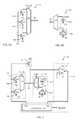
- FIG. 3shows a drive monitoring circuit 302 according to one embodiment.
- a drive monitoring circuit 302can be one of a type of monitor circuit, such as those shown as 102 - 0 to - n in FIG. 1 ).
- a drive monitor circuit 302can include a transistor-under-test (TUT) section 316 , a load section 318 , and a monitor section 320 .
- TUT section 316can include one or more transistors that can be tested for performance. Such transistors can include n-channel transistors, p-channel transistors, or combinations thereof.
- a load section 318can include an impedance that is driven by TUT section 316 in a monitor operation.
- a load section 318can include circuit elements (e.g., capacitors) formed with physical structures of an IC device, to reflect process variations of such structures.
- a monitor section 320can generate a monitor value Mx reflecting a TUT section 316 driving a load section 318 .
- the monitor section 320generates the monitor value Mx by first charging the capacitor to a predetermined first voltage.
- the TUT sectionis configured to be in a non-conductive state while the capacitor is being pre-charged to set a predetermined initial condition prior to the TUT measurement operation.
- the capacitorcan be pre-discharged to set the initial condition. For simplicity we use the terms pre-charged and dis-charged for the setting of the initial conditions and TUT measurement operations, respectively).
- the monitor section 320stops charging the capacitor and configures the TUT section 316 to a conductive state such that the capacitor starts discharging to a second predetermined voltage through the TUT section 316 .
- a drive monitoring circuit 302can be “dominated” by the performance of transistor(s) in TUT section 316 and/or physical features of an IC device reflected by load section 318 . If different TUT sections 316 are used discharge a capacitor that is charged to the same predetermined first voltage, the rate at which the capacitor is discharged through the TUT section 316 represents the speed of the TUT section.
- the rate at which the load section 318 is dischargedrepresents the magnitude of the load resulting from the physical features of the IC device associated with the load section 318 .
- Alternative embodiments of the drive monitoring circuit 302can first discharge the load section 318 to a first predetermined voltage, and subsequently charge it to a second predetermined voltage through the TUT, where the rate of charging the load section 318 can represent the performance of the load section 318 or the TUT section 316 .
- FIG. 4Ais a block schematic diagram of a drive monitor circuit 402 according to an embodiment.
- a drive monitor circuit 402can be one particular implementation of that shown in FIG. 3 .
- a drive monitor circuit 402can include a TUT section 416 , composed of an n-channel TUT 428 having a source-drain path connected between a monitor node 426 and a low power supply voltage VSS, and a gate connected to a “Start” signal generated by a counter circuit 424 .
- the TUT 416can discharge monitor node 426 from a predetermined initial voltage to (or toward) VSS, where the time interval to discharge the monitor node to a reference voltage level Vref is representative of the TUT performance.
- a load section 418can be a capacitance, which in the embodiment shown, is connected between monitor node 426 and low power supply voltage VSS. Load section 418 can be charged to a predetermined voltage by monitor circuit 420 through switch element 421 , and in a subsequent monitor operation, can be discharged by TUT section 416 .
- a monitor circuit 420can include a switch element 421 , a comparator 422 , and a counter circuit 424 .
- a switch element 421can charge monitor node 426 to (or toward) VDD in response to a Start output from counter circuit 424 .
- a comparator 422can have a negative polarity input (labeled “ ⁇ ” in FIG. 4A ) connected to monitor node 426 , a positive polarity input (labeled “+” in FIG. 4A ) that receives a reference voltage Vref, and an output connected to a Stop input of counter circuit 424 .
- a counter circuit 424can generate a count value Mx(count) that corresponds (i.e., is inversely proportional) to a speed at which a load section 418 can be discharged by TUT section 416 .
- counter circuit 424can start a count operation while simultaneously activating a Start signal.
- the activated Start signalcan start a monitor operation by disabling switch element 421 and enabling TUT section 416 , thereby starting the discharge of the load section 418 through the TUT.
- an output of comparator 422goes high, i.e. after the monitor node has discharged to reference voltage Vref, the “Stop” signal is activated and the count operation stops.
- FIG. 4Bis a timing diagram showing one particular monitor operation for the drive monitor circuit 402 of FIG. 4A .
- a Start outputcan be inactive (low).
- Switch element 421can be enabled, and monitor node 426 can charge the capacitance of load section 418 to VDD.
- TUT section 416can be disabled. With monitor node 426 above a Vref, an output of comparator 422 can be low.
- a Start outputis activated (driven high).
- Switch element 421is disabled and TUT section 416 is enabled.
- load section 418starts to discharge toward VSS.
- monitor circuit 420initiates the count operation. The count operation continues as long as the voltage at the monitor node 426 exceeds the reference voltage Vref, and output of comparator 422 remains low.
- a Start outputcan return to the inactive state.
- TUT section 416can be disabled and switch element 421 can be enabled.
- monitor node 426can be pre-charged once again to VDD, and the monitor operation can be repeated.
- FIG. 5is a block schematic diagram of a drive monitor circuit 502 according to another embodiment.
- the drive monitor circuit 502can be one particular implementation of that shown in FIG. 3 .
- a drive monitor circuit 502includes sections corresponding to FIG. 4A , but with reversed transistor conductivity types. Thus, a count value Mx(count) can reflect the performance of a p-channel TUT section 516 and/or load section 518 .
- the TUT section 516 of the drive monitor circuit 502is composed of a p-channel TUT having a source-drain path connected between a monitor node 526 and a high power supply voltage VDD, and a gate connected to a “StartN” signal generated by a counter circuit 524 .
- the TUT section 516can charge the monitor node 526 from a predetermined initial voltage (which is a negative voltage in this embodiment) to (or toward) VDD, where the time interval to charge the monitor node to a reference voltage level Vref is representative of the performance of the TUT section 516 .
- the load section 518can be a capacitance, which in the embodiment shown is connected between the monitor node 526 and the high power supply voltage VDD.
- the monitor circuit 520can include a switch element 521 , a comparator 522 , and a counter circuit 524 .
- the “StartN” signal generated by the counter circuit 524is an active-low signal that starts the monitor operation when it is at a low voltage level.
- the switch element 521pre-discharges the monitor node 526 towards VSS, and therefore, the load section 518 is discharged until the voltage across the load section 518 is ⁇ VDD (or negative VDD).
- the counter circuit 524starts a count operation and simultaneously activates the “StartN” signal by placing a low voltage level on that signal.
- the activated “StartN” signalstarts the monitor operation by disabling switch element 521 and enabling the TUT section 516 , thereby starting to charge the load section 518 through the TUT section 516 .
- the charging of the load sectioncontinues either as long as the “StartN” signal is asserted, or until the monitor node voltage reaches VDD (i.e., the load section 518 has been charged such that the voltage across the load section 518 increases from ⁇ VSS to VDD).
- the output of the comparator 522goes high after the monitor node voltage exceeds the reference voltage Vref. This activates the “Stop” signal and stops the count operation of the counter circuit 524 .
- the resulting count value after the count operation has stoppedis the monitor value Mx(count).
- FIG. 6Ais a block schematic diagram of a TUT section 616 that can be included in embodiments. TUT section 616 can be one particular implementation of that shown as 416 in FIG. 4 ). A TUT section 616 can select one of multiple transistors ( 628 - 0 to - i ) for a monitoring operation.
- a TUT section 616can include multiple TUTs ( 628 - 0 to - i ) and a multiplexer (MUX) 630 .
- TUTscan include a low threshold voltage transistor (LVT), a standard threshold voltage transistor (SVT) (which is slower than LVT transistors), and a high threshold voltage transistor (HVT) (which is slower than both SVT and LVT transistors).
- LVTlow threshold voltage transistor
- SVTstandard threshold voltage transistor
- HVThigh threshold voltage transistor
- TUTscan include transistors having other differences (e.g., doping profiles, width/length ratios, oxide thicknesses, etc.).
- FIG. 6Ashows n-channel device, other embodiments can include p-channel transistors.
- a MUX 630can be formed from the same device types as corresponding TUTs (i.e., n-channel, p-channel). That is, a charge/discharge path flows through a transistor(s) having a same conductivity type.
- a MUX 630can include signal paths formed by complementary conductivity (e.g., CMOS) devices, which can introduce substantially no threshold voltage drop into the charge/discharge path. Regardless, the conductivity of the MUX should be much greater than that of the TUT so that the result is not significantly impacted. Alternatively, the weights and Vref on the comparator can be adjusted so that the measurement results properly represents the TUT and load combination.
- Switching in different TUT typescan enable a monitor value to represent the performance of such a transistor type.
- FIG. 6Bis a block schematic diagram of a load section 6718 that can be included in embodiments.
- Load section 618can be one particular implementation of that shown as 418 in FIG. 4A or 518 in FIG. 5 ).
- a load section 618can select one of multiple loads ( 634 - 0 to - j ) for a monitoring operation.
- a load section 618can include multiple loads ( 634 - 0 to - j ) and a multiplexer (MUX) 632 .
- loadscan include capacitors formed by various structures of an IC device, and hence can reflect process variations of the device.
- one capacitance 634 - 0can be a metal-metal capacitor having one plate formed by a metallization layer(s), a second plate formed by metallization layer(s), and a dielectric formed by one or more interlayer dielectric(s).
- another capacitance 634 - jcan be a transistor capacitance having one plate formed by a transistor gate, a second plate formed by a substrate (source/drain/channel), and a dielectric formed by a gate capacitance and diffusion capacitance.
- loads ( 634 - 0 to - j )can include other impedance types, or combinations of impedances, such as resistance, inductance, etc.
- Switching in different load typescan enable a monitor value to represent the delay caused by the capacitance presented by such a load type. Additionally, in the presence of systemic variation of the IC, the monitor value can also represent the performance impact resulting from such variations.
- FIG. 7is a block schematic diagram of a drive monitor circuit 702 according to another embodiment.
- a drive monitor circuit 702can be one particular implementation of that shown in FIG. 3 .
- a drive monitor circuit 702can include sections like those of FIG. 4A , including a TUT section 716 and a load section 718 .
- a TUT section 716can take a form like that of FIG. 6A , enable the selection of any of a number of different TUTs 728 - 0 to 728 - i . While FIG. 7 shows a TUT section 716 with n-channel TUTs, TUT section 716 can include p-channel TUTs as well.
- a MUX 730can selectively connect one or more TUTs ( 728 - 0 to 728 - i ) to monitor node 726 .
- a load section 718can take the form of that shown in FIG. 6B , enabling the selection of any of a number of different loads 734 - 0 to 734 - j.
- a drive monitor circuit 702can evaluate circuit element performance by executing different monitor operations, as described herein or equivalents, that select different combinations of TUTs ( 728 - 0 to 728 - i ) with different loads ( 734 - 0 to 734 - j ). It is understood that such different monitor operations can select a single TUT and a single load, multiple TUTs and a single load, a single TUT and multiple loads, as multiple TUTs with multiple loads.
- the monitor section 720can evaluate the performance of one or more transistors included in the TUT section 716 by performing a monitor operation for each of the transistors while setting the select input Z_SEL to connect the same capacitor of the load section 718 to the monitor node 726 .
- the monitor section 720selects one of the TUTs of the TUT section 716 using the TUT_SEL input (e.g., TUT0, . . . , TUTi) and generates the monitor value Mx for the selected TUT by first charging the load section 718 to a predetermined first voltage.
- TUT_SEL inpute.g., TUT0, . . . , TUTi
- the TUT section 716is configured to be in a non-conductive state while the load section 718 is being charged.
- the monitor operationis started by asserting the “Start” signal of the counter circuit 724 and simultaneously starting the count operation of the counter circuit 724 . This stops the charging of the load section 718 and configures the selected TUT of the TUT section 716 to a conductive state such that the load section 718 starts discharging to VSS through the selected TUT.
- This discharging of the load section 718continues either as long as the “Start” signal is asserted, or until the monitor node voltage reaches VSS (i.e., the load section 718 has been discharged such that the voltage across the load section 718 decreases from VDD to VSS).
- the output of the comparator 722goes high after the monitor node 726 voltage goes below the reference voltage Vref. This activates the “Stop” signal and stops the count operation of the counter circuit 724 .
- the resulting count value after the count operation has stoppedis the monitor value Mx(count).
- the performance of additional TUTs in the TUT sectionare evaluated by charging the load section 718 to VDD, setting TUT_SEL input to a value that selects the next TUT of the TUT section 716 that is to be evaluated, and performing another monitor operation by activating the start signal to obtain the monitor value Mx for the next TUT. This process can be repeated to obtain the monitor value for additional TUTs in the TUT section 718 .
- the monitor circuit 702can evaluate the performance impact resulting from different process variations and physical features of the IC device by performing the monitor operation for corresponding loads of the load section 718 , e.g. 734 - 0 . . . j , under the control of the load select signal Z_SEL, while using the same TUT section to discharge the selected load section, then the rate at which the selected load section is discharged represents the performance impact of the load resulting from the process variation or physical feature of the IC device associated with the selected load.
- the value of the load select signal Z_SELcan be changed to select additional loads in the load section 718 , and the steps for charging the monitor node 726 and subsequently discharging it using the same TUT section can be repeated to evaluate the performance impact of additional sources of process variation or physical features of the ID device.
- FIG. 8is a diagram showing one particular example of a metal-metal (M-M) capacitor 834 that can be included in embodiments.
- M-M capacitor 843can include plate members formed by interdigitated metallization layers. Plate members 840 - 0 / 1 can be formed by a lower metallization layer. Plate members 838 - 0 / 1 formed by another metallization layer formed over members 840 - 0 / 1 . Plate members 836 - 0 / 1 formed by another metallization layer formed over members 838 - 0 / 1 .
- M-M capacitor 834can be formed by members 836 - 0 / 838 - 0 / 840 - 0 conductively connected together by vertical interconnects 837 - 0 / 1 .
- Another plate of M-M capacitor 834can be formed by members 836 - 1 / 838 - 1 / 840 - 1 conductively connected together by vertical interconnects 837 - 0 / 1 .
- Such M-M capacitorscan be readily designed to match the IC timing paths, e.g., having the same line to line spacing on the same layers, as well as the requisite crossing widths and orientations so as to mimic signal lines on the IC.
- M-M capacitorscan be formed with single interdigitated metallization layer, to monitor a capacitance arising from lateral separation of wirings.
- other M-M capacitorscan be formed by vertically stacked metallization layers, to monitor a capacitance arising from vertical separation of wirings.
- FIG. 9is a diagram showing how differences in conductive layers can introduce variations in capacitance.
- FIG. 9shows different conductive layers in relation to one another.
- Metallization layerscan have different vertical thickness (e.g., tM4, tM5, tM6 . . . tMj, tMk), different horizontal widths (e.g., W4 . . . Wm), different vertical separation (dV4, dV5 . . . dVj, dVk) created by interlayer dielectrics, and different lateral separation (pitch) (e.g., S4 . . . Sm).
- tM4, tM5, tM6 . . . tMj, tMkdifferent horizontal widths
- dV4, dV5 . . . dVj, dVkdifferent vertical separation
- Pitche.g., S4 . . . Sm
- a capacitance between such layerscan vary according to process variation. Accordingly, by including capacitors formed by combinations of metallization layers as load elements in monitoring sections, the effect of such processes variation can be compensated for, to optimize circuit performance.
- FIG. 10is a block schematic diagram of an IC device 1000 according to one embodiment.
- An IC device 1000can be one particular implementation of that shown as 100 in FIG. 1 .
- An IC device 1000can include a combination logic section 1004 , an n-type body bias circuit 1006 - 0 , a p-type body bias circuit 1006 - 1 , and monitoring sections (not shown) that provide monitoring values to combination logic section 1004 .
- an n-type body bias circuit 1006 - 0can include a charge pump 1047 and a frequency adjust (frequency control) circuit 1046 .
- a charge pump 1047can drive its output Vbn to a potential based on a clock signal CLK_Q.
- Frequency adjust circuit 1046can generate clock signal CLK_Q according to bias control values NBias, which can be generated as described for embodiments herein, or equivalents.
- bias control values NBiascan be generated as described for embodiments herein, or equivalents.
- an NBias valuecan cause frequency adjust circuit 1046 to increase the frequency of CLK_Q.
- an NBias valuecan cause frequency adjust circuit 1046 to decrease the frequency of CLK_Q.
- a p-type body bias circuit 1006 - 1can include a switched capacitor network 1045 and a switch control circuit 1044 .
- a switched capacitor network 1045can drive its output Vbp to a potential based on a switch control network 1044 .
- Switch control network 1044can generate control signals based on bias control values PBias, which can be generated as described for embodiments herein, or equivalents.
- Body bias circuits as described hereincan generate forward body bias voltages VFB and reverse body bias voltages VBB.
- a forward body bias voltagecan be generated by creating a voltage offset from a generated body bias voltage.
- FIG. 11One such embodiment is shown in FIG. 11 .
- FIG. 11is a block schematic diagram of a power switching circuit 1100 according to an embodiment.
- a power switching circuit 1100can include a p-type body bias circuit 1106 - 1 , a voltage offset circuit 1148 , a mode select MUX 1150 , a power switching device 1152 , and a load section 1156 .
- a power switching circuit 1100can provide a low impedance power supply path to a load 1156 that can vary according to mode of operation.
- a p-type body bias circuit 1106 - 1can generate a body bias voltage Vbp based on bias control values PBias.
- Bias control values PBiascan be generated according to weighted monitor values, as described herein. That is, PBias can be a function of one or more monitor values (Mx) weighted by one or more weight values (Wx).
- a body bias voltage Vbpcan be a reverse body bias voltage VRB that can increase a threshold voltage and decrease leakage of a p-channel transistor.
- a voltage offset circuit 1148can generate a voltage having a predetermined offset with respect to a received voltage.
- an offsetcan be a voltage lower than a received voltage.
- V1can be a forward body bias voltage VFB.
- a voltage offset circuitcan be a Widlar voltage source circuit, but any suitable offset circuit can be employed.
- a mode select MUX 1150can selectively apply either Vbp or V1 as a body bias voltage for power switching device 1152 .
- mode select MUX 1150can apply V1 as a body bias voltage, to lower a threshold voltage of a switching device 1152 .
- mode select MUX 1150can apply Vbp as a body bias voltage, to increase a threshold voltage of a switching device 1152 .
- a switching device 1152can be one or more p-channel transistors having a body connected to an output of mode select MUX 1150 , a source connected to a high power supply VDD, a drain connected to an internal power supply node 1158 , and a gate connected to receive an enable signal EN. By operation of switching device 1152 , a voltage VDD_PG can be generated at internal power supply node 1158 , to provide power to load section 1156 .
- a load section 1156can be connected between internal power supply node 1158 and a low power supply VSS.
- a load section 1156can include a circuit that provides some predetermined function for the IC device containing the power switching circuit 1100 .
- FIG. 12is a block schematic diagram of a core biasing circuit 1256 that can be used in an embodiment like that of FIG. 11 .
- core biasing circuit 1256can correspond to load section 1156 of FIG. 11 .
- a core biasing circuit 1256can include a “core” section 1262 and a core bias MUX 1260 .
- a core section 1262can perform a predetermined function, and can include complementary (i.e., p-channel and n-channel) transistors, having bodies that receive adjustable body bias voltages (Vpcore, Vbn).
- a core section 1262can be formed between an internal power supply node 1258 VDD_PG and a low power supply node VSS.
- an internal power supply node 1258 VDD_PGcan correspond to that shown as 1158 in FIG. 11 (i.e., it can be switched between a high body bias Vbp and a lower VFB of V1).
- n-channel transistors of core section 1262can have bodies biased to a voltage Vbn.
- a voltage Vbncan be a generated according to embodiments shown herein, or equivalents.
- Bodies of p-channel transistors of core section 1262can be biased according to an output from core bias MUX 1260 .
- Core bias MUX 1260can selectively apply either a body bias voltage Vbp or the voltage at internal power supply node VDD_PG (which can be less than Vbp), according to a mode value MODE_SEL. More particularly, in one mode (e.g., an active or high performance mode), core bias MUX 1260 can apply VDD_PG as a body bias voltage. In a second mode (e.g., an inactive or low leakage mode), core bias MUX 1260 can apply Vbp as a body bias voltage. Such a local switching of the p-channel wells of core section 1262 can reduce band to band tunneling junction current when a switching device (i.e., 1152 of FIG. 11 ) is off, and VDD_PG can be at a relatively low voltage.
- a switching devicei.e., 1152 of FIG. 11
- body biasingas described for a power gating switch in FIG. 11 , can also be applied to a device that supplies a regulated voltage.
- a device that supplies a regulated voltageOne such embodiment is shown in FIG. 13 .
- FIG. 13is a block schematic diagram of a regulator circuit according to an embodiment.
- a regulator circuit 1300can include sections like those of FIG. 11 , including a p-type body bias circuit 1306 - 1 , a voltage offset circuit 1348 , and a mode select MUX 1350 . Such like sections can operating in the same fashion as those shown in FIG. 11 , or equivalents.
- a voltage regulating circuit 1300can also include a low dropout regulator (LDO) section 1368 and core section 1362 .
- An LDO section 1368can include a regulating device 1352 , a mode control MUX 1364 , and an amplifier 1366 .
- a regulating device 1352can be a p-channel transistor having a body connected to an output of mode select MUX 1350 , a source connected to a high power supply VDD, a drain connected to a regulated node 1358 , and a gate connected to receive a regulation control voltage Vreg, output from mode control MUX 1364 .
- a mode control MUX 1364can selectively output either a high power supply voltage VDD or an output of amplifier 1366 .
- mode control MUX 1364can apply the output of amplifier 1366 , which can drive a gate of regulating device 1352 to maintain regulated node 1358 at a predetermined voltage.
- mode control MUX 1364can apply VDD as a body bias voltage, to turn off regulating device 1352 .
- An amplifier 1366can provide an output that can vary according to a feedback voltage Vfdbk provided from core section 1362 . Thus, if a voltage at regulated node 1358 is too low, Vfdbk can fall below Vref, and an output of amplifier 1366 can be driven lower. Conversely, if a voltage at regulated node 1358 is too high, Vfdbk can rise above Vref, and an output of amplifier 1366 can be driven higher.
- a core section 1362is represented by load sections 1356 - 0 and 1356 - 1 . It is understood that such sections ( 1356 - 0 / 1 ) can represent circuits for performing the various functions of an IC device.
- Body biasing as described for embodiments hereincan be applied to bodies of various transistor types. Examples of some transistor types which can receive a body bias voltage are shown in FIG. 14A to 15 .
- FIG. 14Ashows a bulk substrate n-channel transistor 1470 -A, in which a transistor body can be biased via a bulk substrate 1408 -A.
- FIG. 14Bshows a p-channel transistor 1470 -B formed in an n-type well, formed in a p-type substrate. In such a transistor, a body can be biased via well 1408 -B.
- FIGS. 14C and 14Dshow a semiconductor-on-insulator type transistor (e.g., silicon-on-insulator, SOI) having an active semiconductor region 1475 separated in a vertical direction from a bulk substrate 1472 by an insulating layer 1474 .
- Active region 1475can be separated in a lateral direction from other active regions (not shown) by lateral insulating structures 1476 .
- FIG. 14Cshows an n-channel transistor 1470 -C having source and drain regions that do not extend to insulating layer 1474 .
- a body regioncan be biased via body region 1408 -C.
- FIG. 14Dshows an n-channel transistor 1470 -C having source and drain regions that extend to insulating layer 1474 .
- a body regioncan be biased via body region 1408 -D.
- FIG. 15Ashows a deeply depleted channel (DDC) type transistor 1570 , which can be included in embodiments.
- DDC transistor 1570can be configured to have an enhanced body coefficient, along with the ability to set a threshold voltage (Vt) with enhanced precision.
- a DDC transistor 1570can include a gate electrode 1582 , source 1584 , drain 1586 , and a gate dielectric 1588 positioned over a substantially undoped channel 1511 .
- Optional lightly doped source and drain extensions (SDE) 1590can be positioned respectively adjacent to source 1584 and drain 1586 . Such extensions 1590 can extend toward each other, reducing effective length of the substantially undoped channel 1511 .
- SDElightly doped source and drain extensions
- the DDC transistor 1570is shown as an n-channel transistor having a source 1584 and drain 1586 made of n-type dopant material, formed upon a substrate such as a p-type doped silicon substrate providing a p-well 1517 .
- the n-channel DDC transistor 1570 in FIG. 15Acan include a highly doped screening region 1515 made of p-type dopant material, and a threshold voltage set region 1513 made of p-type dopant material.
- FIG. 15Bshows FinFET type transistor 1570 -B which can be included in embodiments.
- the FinFET transistor 1570 -Bcan include a gate electrode 1582 -B and gate dielectric 1588 -B that surround a substantially undoped channel 1511 -B on opposing sides.
- the view of FIG. 15Bis taken along a channel length.
- source and drain regionscan extend into and out of the view shown. Further, such source and drain regions can be separated from screening region 1515 -B by portions of undoped channel region 1511 -B.
- FIG. 15Cshows a FinFET type transistor 1570 -C having a screening region 1515 -C which can be included in embodiments.
- the FinFET transistor 1570 -C having a screening regioncan be configured to have an enhanced body coefficient, along with the ability to set a Vt with enhanced precision.
- the transistor 1570 -Cincludes a gate electrode 1582 -C and gate dielectric 1588 -C formed over a substantially undoped channel 1511 -C on opposing sides.
- a highly doped screening region 1515 -Cis formed in a substrate 1519 below substantially undoped channel 1511 -C.
- a Vt set region 1513 -Cis formed between the screening region 1515 -C substantially undoped channel 1511 -C.
- FIG. 15Cis taken along a channel length, and source and drain regions can extend into and out of the view, separated from screening region 1515 -C by portions of undoped channel region 1511 -C.
- Embodiments of various structures and manufacturing processes suitable for use in DDC transistorsare disclosed in U.S. patent application Ser. No. 12/708,497, filed on Feb. 18, 2010, titled Electronic Devices and Systems, and Methods for Making and Using the Same, by Scott E. Thompson et al.; U.S. Pat. No. 8,273,617, issued on Sep. 25, 2012, titled Low Power Semiconductor Transistor Structure and Method of Fabrication Thereof; U.S. patent application Ser. No. 12/971,955 filed on Dec. 17, 2010 titled Transistor with Threshold Voltage Set Notch and Method of Fabrication Thereof; U.S. patent application Ser. No. 12/895,785 filed on Sep.
- conductivities of any of the transistors described abovecan be switched (i.e., from p-channel to n-channel and vice versa).
- FIG. 16A-0is a graph showing performance variations of n-channel TUTs in a circuit like that of FIG. 4A .
- Curve 1651shows transistor performance for a “slow” n-channel TUT.
- Curve 1653shows transistor performance for a “fast” n-channel TUT.
- Curve 1655shows a nominal transistor performance for an n-channel TUT.
- the n-channel TUTs of FIG. 16A-0are DDC transistors like that shown in FIG. 15 , having a reverse body bias voltage of 0.3V, and source-drain voltage (VDS) of 0.9V.
- VDSsource-drain voltage
- a monitor circuitcan determine the performance of the TUT by determining the duration of time taken by a monitor node voltage to dis-charge from an initial voltage level to a predetermined voltage level. For example, in the embodiment shown in the figure, the monitor circuit determines three different performance levels for the TUT (shown as t_fast, t_nom, and t_slow) by determining the time (e.g. count) at which the voltage at the monitor node falls below 0.44V.
- FIG. 16A-1is a graph showing how an adjustment of a body bias can compensate for variations in transistor performance.
- Curve 1651 ′shows a “slow” n-channel device performance after the body bias has been adjusted in the forward body bias direction to 0.04V. As shown, after such an adjustment, the slow n-channel transistor can closely follow the nominal case 1655 .
- curve 1653 ′shows a “fast” n-channel device performance after the body bias has been adjusted in the reverse body bias direction to 0.46V. As shown, after such an adjustment, the fast n-channel transistor now closely follows the nominal case 1655 .
- FIG. 16B-0is a graph showing performance n-channel TUTs like that of FIG. 16A-0 , but at a lower source-drain voltage (VDS) of 0.6V, and a capacitive load that is 20% of that used for FIG. 16A-0 .
- VDSsource-drain voltage
- curve 1671shows transistor performance for a slow n-channel TUT
- curve 1673shows transistor performance for a fast n-channel TUT
- curve 1675shows a nominal transistor performance for an n-channel TUT.
- Speeds of transistorscan are based on the time (e.g., count) when a monitor node falls below 0.3V (shown again as t_fast, t_nom, and t_slow).
- FIG. 16B-1shows how adjustment of a body bias can compensate for variations in transistor performance in the same manner as FIG. 16A-1 (but with different body bias adjustments).
- a body bias voltagecan be adjusted to bring a transistor performance within a desired limit.
- a body bias voltagecan be adjusted to enable the devices to have similar or substantially identical performance to the nominal case.
- the ICcan have its systematic variability compensated towards the nominal IC performance, thereby limiting IC non-uniformity due to manufacturing variations.
- FIG. 17shows one embodiment of a bias voltage distribution network that uses monitor circuits to implement a fine grained body biasing technique.
- FIG. 17shows an integrated circuit 1700 , with four functional blocks 1702 , 1704 , 1706 , and 1708 .
- Functional block 1702includes a monitor circuit 1710 and a body bias tuning circuit 1712
- functional block 1704includes a monitor circuit 1714 and a body bias tuning circuit 1716
- functional block 1706includes a monitor circuit 1718 and a body bias tuning circuit 1720
- functional block 1708includes a monitor circuit 1722 and body bias tuning circuit 1724 .
- the functional blocks 1702 - 1708can be SRAM arrays having different sizes or different performance targets, graphics processors, general purpose processors, memory controllers, etc.
- the design of one or more of the functional blocks 1702 - 1708can be the same as one of the other functional blocks on the integrated circuit, where the different identically designed functional blocks are configured to operate at different performance targets (e.g., speed, power consumption, etc.) by the application of different body bias voltages.
- the integrated circuit 1700can be divided into several regions, instead of functional blocks where each region has a monitor circuit and a body bias tuning circuit.
- the integrated circuit 1700uses one body bias generator 1750 that generates a pmos body bias voltage and an nmos body bias voltage sufficient to provide the highest body bias voltage that is to be supplied to the p-channel and n-channel transistors, respectively, of the functional blocks in the integrated circuit 1700 .
- the nmos and pmos body bias voltages generated by the body bias generator 1750are distributed to the functional blocks 1702 - 1708 using wires 1752 and 1754 , respectively.
- the body bias tuning circuit at each functional blockreceives the body bias voltages on the wires 1752 and 1754 , and generates local pmos and nmos body bias voltages for the corresponding functional block in accordance with the body bias control signal received from the monitor circuit of that functional block.
- the body bias generator 1750can generate only one body bias voltage, and only one wire can be used to distribute that body bias voltage to the functional blocks in the integrated circuit.
- FIG. 18shows one embodiment of the bias tuning circuit using a resistive divider 1805 to generate the local body bias voltage 1815 .
- the voltage 1810is received from the body bias generator, and different body bias voltages are generated using the resistive divider 1805 .
- the number of resistors (R) and the values of the resistors in the resistive dividerare determined in accordance with the different body bias voltages to be provided to the corresponding functional block.
- a switch network 1825receives the voltages generated by the resistive divider and connects the generated voltage selected by the bias voltage select signal 1820 to the local body bias voltage terminal 1815 .
- the body bias voltage select signalis received from the monitor circuit of the functional block.
Landscapes
- Physics & Mathematics (AREA)
- Engineering & Computer Science (AREA)
- Computer Hardware Design (AREA)
- Computing Systems (AREA)
- General Engineering & Computer Science (AREA)
- Mathematical Physics (AREA)
- Semiconductor Integrated Circuits (AREA)
Abstract
Description
The present invention relates generally to integrated circuit (IC) devices, and more particularly to body bias circuits and methods for insulated gate field effect transistors of IC devices.
Integrated circuit (IC) devices can be subject to manufacturing variations that can impact performance. In a typical IC device, electrical signals can be transmitted via an interconnect structure formed by multiple metallization layers, separated from one another by interlayer dielectrics (ILDs). Signals can be generated by transistors driving metallization layers between different potentials.
Many fabrication processes utilize chemical-mechanical polishing (CMP) to planarize ILD surfaces. While CMP can improve planarization over other fabrication methods, it can still impart systematic and random thickness variations at the lot, wafer, die and pattern levels. Die level variation in such structures can result in performance and timing differences in the same type of devices. In particular, signal transmission paths can be affected by variations in metal-metal capacitance inherent in an interconnect structure. Differences in metal-metal capacitance can arise from variations in dielectric thickness between metallization lines and/or variations in metal thickness and width. Differences in resistance can also arise from such variations in metal thickness and width.
Active devices (e.g., transistors) may also be subject to some variation in performance. For example, uncontrollable manufacturing variations can result in “fast” transistors and “slow” transistors. Fast transistors can provide faster driving capability than slow transistors. Such fast vs. slow variations can be systematic, i.e., they can affect the mean value of performance parameters.
These and other variations can result in IC devices having differing performance limits. Conventionally, timing paths can be designed with sufficient margin to be adequate for a slowest case. This can require large signal driving devices and increased power consumption, as well as increased design effort. For some very high performance IC devices, such variations can present a limit to device speed and/or reliability.
Various embodiments of the present invention will now be described in detail with reference to a number of drawings. The embodiments show integrated circuits and methods for biasing bodies of transistors in an integrated circuit device, where such biasing can be based on performance of actual circuit structures present on the integrated circuit device.
In the various embodiments below, like items are referred to by the same reference character but the leading digits corresponding to the figure number.
Each monitoring section (102-0 to -n) can include physical circuit elements of theIC device 100 that can vary according to process variation. Monitoring sections (102-0 to -n) can output monitor values M0 to Mn that reflect variations in performance resulting from variations in process. In particular embodiments, each monitoring section (102-0 to -n) can provide a monitor value (M0 to Mn) that is dominated by one or more particular process features. In the particular embodiment shown, monitor sections (102-0 to -n) include those dominated by: n-type transistor performance, p-type transistor performance, wiring, and diffusion. It is understood that such features are but exemplary. In some embodiments, a monitoring section can include a ring oscillator circuit having an oscillating frequency reflecting the effect of one or more sources of process variations. However, in particular embodiments, a monitoring section can include a transistor drive monitoring section, embodiments of which are described in more detail below.
Monitor sections (102-0 to -n) can provide monitor values in various ways. For example, in some embodiments or modes of operation, monitor sections (102-0 to -n) can be operational during a test or characterization phase. Monitor values (M0 to Mn) generated in the test/characterization phase can be stored such that they remain fixed throughout the operation of the device. After the monitor values have been generated, thecombination logic section 104 can access the stored monitor values to set the n-type and p-type transistor body bias voltages based on one or more of the stored monitor values during the operation of the device. The monitor values can be stored in internal storage that is part of thecombination logic section 104, or in external storage that is located outside thecombination logic section 104 and accessed by thecombination logic section 104.
In other embodiments or modes of operation, monitor sections (102-0 to -n) can be activated periodically and/or constantly, allowing monitor values to be updated while the device is in operation. In such embodiments, acombination logic section 104 can receive the periodically or continuously updated monitor values (102-0 to -n) and modify the n-type and p-type body bias voltages based on the updated monitor values.
In still other embodiments or modes of operation, monitor sections (102-0 to -n) can be enabled in response to a command input to theIC device 100, where the monitor sections generate and store updated monitor values during a test/characterization phase that is initiated in response to receiving the command input at the IC device. In other embodiments, the monitor sections (102-0 to -n) can be enabled in response to received status information indicative of particular conditions or changes to particular conditions (e.g., power-on, reset, temperature, power supply voltage, etc.). For example, the test/characterization phase can be initiated if temperature exceeds a predetermined threshold value, such that monitor sections (102-0 to -n) are enabled to generate and store updated monitor values that are used to modify the n-type and p-type body bias voltages.
Acombination logic section 104 can receive monitor values (M0 to Mn), and from such values, generates n-type and p-type body bias control values (NBias, PBias). In particular embodiments, acombination logic section 104 can assign different weights to one or more of the monitor values (M0 to Mn) such that particular monitor values (M0 to Mn) have a greater weight over others, to reflect how one type of process variation can have a greater effect than other types of process variations on a particular performance characteristic of a circuit within theIC device 100. In this way, body biases can be tuned to optimize an IC device for a particular performance target. In some embodiments, bias control values (NBias, PBias) can be static during the operation of theIC device 100. However, in other embodiments, such values can be static, changing according to mode of operation, and/or operating conditions. Additionally, the weights can compensate for differing sensitivities of the monitoring circuits to the variations, as well as the IC's sensitivity to such variations.
It is noted that bias control values (NBias, PBias) generated by acombination logic section 104 can be digital or analog values.
An n-type body bias circuit106-0 can receive a bias control value (NBias), and in response generate an n-channel transistor body bias voltage (Vbn). That is, a voltage Vbn can vary according to the bias control value NBias. In very particular embodiments, Vbn can vary from a “back bias” level (VBB) to a forward bias level (VFB). A back bias level can force a body region below a low power supply voltage (e.g., less than VSS) to increase a threshold voltage, but lower a switching speed of an n-type transistor (as compared to such a transistor having a body bias of VSS). In contrast, a forward bias level can force a body region above a low power supply voltage (e.g., greater than VSS) to lower a threshold voltage of a transistor, but increase a switching speed of an n-type transistor (as compared to such a transistor having a body bias of VSS).
In a similar fashion, a p-type body bias circuit106-1 can receive a bias control value (PBias), and in response, generate a p-channel transistor body bias voltage (Vbp). In certain embodiments, Vbp can vary from a “back bias” level (e.g., greater than a high power supply voltage VDD) to a “forward bias” level (e.g., less than VDD).
Anoperational section 150 can include transistors formed with body regions that can receive the body bias voltages (Vbn, Vbp). Such transistors can be arranged to provide a predetermined function as part of different functional blocks having different predetermined target performance characteristics, where the performance of each functional block can be independently adjusted by selection of the n-type and p-type body bias voltages. Accordingly, anoperational section 150 can include n-type transistors formed in p-type body regions108-0, and p-type transistors formed in n-type body regions108-1. Body regions (108-0/1) can vary according to transistor type. Various examples of transistors that can have a body bias will be described in more detail below.
Body bias voltages (Vbn, Vbp) can be applied to transistors ofoperational section 150 to compensate for process variations detected by monitoring sections (102-0 to -n). Thus, if a metallization structure presents a high capacitance, resulting in a slower signal transmission speed, a body bias voltage can be lowered, to increase the driving speed of the transistors in the device. Similarly, if such transistors are considered “slow” transistors, a body bias voltage can be reduced or increased, for p-type and n-type transistors respectively, to bring the performance of the transistors back into a desired speed range. The opposite type of adjustment is possible as well. If metallization presents a smaller capacitance or transistors are “fast”, a body bias can be increased or decreased to compensate for these variations by corresponding changes of the transistor speeds in response to the applied body bias.
Aweight value store 212 can provide weight values (W0 to Wi) to increase or decrease the effect that a monitor value can have on a resulting bias control value (PBias, NBias), typically achieved by multiplying the monitor value by the corresponding weight value. In some embodiments, weight values (W0 to Wi) can be determined through simulation or characterization of circuits within an integrated circuit device. In other embodiments, weight values (W0 to Wi) can be established by testing integrated devices of a same manufacturing group (e.g., lot), or by circuits on the device itself (such as monitor sections, described herein). Once such weight values are determined, the values (W0 to Wn) can remain fixed during the operation of the device, or alternatively, can be updated during the operation of the device. Amonitor value store 210 can be formed with any suitable storage elements, including non-volatile elements, volatile storage elements (e.g., flash memory, fuses, SRAM, latches), or combinations of thereof. In the case of fixed weight values, a back end process, such as the opening of fusible links can be used to set the weight values.
A biasvalue generator circuit 214 can apply weighting values (W0 to Wn) to corresponding monitor values (M0 to Mn), and combine the results to generate bias control values (NBias, PBias) that are responsive to the weighting values (W0 to Wn) and the monitor values (M0 to Mn). A biasvalue generator circuit 214 can include any circuits suitable for combining/weighting monitor values. In some embodiments, a biasvalue generator circuit 214 can be an analog circuit, combining/multiplying voltages or currents. In other embodiments, a biasvalue generator circuit 214 can be a digital circuit, combining digital values through operations such as binary addition and multiplication. In the latter case, a biasvalue generator circuit 214 can be formed with custom logic, programmable logic, and/or can include a processor executing predetermined instructions.
It is noted that acombination logic section 204 can also modify a bias control value in response to additional control parameters. As but one example, the bias control values (e.g., NBias and/or PBias) can be adjusted according to a power supply voltage of the device. Such one or more of the bias control values can be adjusted by a predetermined amount if a change on the power supply voltage exceeds a threshold value. Such adjustments can be performed by directly modifying the bias control values, modifying the stored monitor values (M0 to Mn), or adjusting the weights (W0 to Wn) in response to received values of the control parameters.
Aload section 318 can include an impedance that is driven byTUT section 316 in a monitor operation. In some embodiments, aload section 318 can include circuit elements (e.g., capacitors) formed with physical structures of an IC device, to reflect process variations of such structures.
Amonitor section 320 can generate a monitor value Mx reflecting aTUT section 316 driving aload section 318. For example, in embodiments where theload section 318 is a capacitor, themonitor section 320 generates the monitor value Mx by first charging the capacitor to a predetermined first voltage. Typically, the TUT section is configured to be in a non-conductive state while the capacitor is being pre-charged to set a predetermined initial condition prior to the TUT measurement operation. (In certain embodiments, the capacitor can be pre-discharged to set the initial condition. For simplicity we use the terms pre-charged and dis-charged for the setting of the initial conditions and TUT measurement operations, respectively). After the capacitor has been charged to the predetermined first voltage, themonitor section 320 stops charging the capacitor and configures theTUT section 316 to a conductive state such that the capacitor starts discharging to a second predetermined voltage through theTUT section 316. Thus, adrive monitoring circuit 302 can be “dominated” by the performance of transistor(s) inTUT section 316 and/or physical features of an IC device reflected byload section 318. Ifdifferent TUT sections 316 are used discharge a capacitor that is charged to the same predetermined first voltage, the rate at which the capacitor is discharged through theTUT section 316 represents the speed of the TUT section. Alternatively, if different load sections or different capacitors that are representative of different physical features of the IC device are charged to the same first predetermined voltage, and the same TUT section is used to discharge these load sections, then the rate at which theload section 318 is discharged represents the magnitude of the load resulting from the physical features of the IC device associated with theload section 318. Alternative embodiments of thedrive monitoring circuit 302, can first discharge theload section 318 to a first predetermined voltage, and subsequently charge it to a second predetermined voltage through the TUT, where the rate of charging theload section 318 can represent the performance of theload section 318 or theTUT section 316.
Aload section 418 can be a capacitance, which in the embodiment shown, is connected betweenmonitor node 426 and low power supply voltage VSS.Load section 418 can be charged to a predetermined voltage bymonitor circuit 420 throughswitch element 421, and in a subsequent monitor operation, can be discharged by TUT section416.
Amonitor circuit 420 can include aswitch element 421, acomparator 422, and acounter circuit 424. Aswitch element 421 can charge monitornode 426 to (or toward) VDD in response to a Start output fromcounter circuit 424. Acomparator 422 can have a negative polarity input (labeled “−” inFIG. 4A ) connected to monitornode 426, a positive polarity input (labeled “+” inFIG. 4A ) that receives a reference voltage Vref, and an output connected to a Stop input ofcounter circuit 424.
Acounter circuit 424 can generate a count value Mx(count) that corresponds (i.e., is inversely proportional) to a speed at which aload section 418 can be discharged by TUT section416. In particular,counter circuit 424 can start a count operation while simultaneously activating a Start signal. The activated Start signal can start a monitor operation by disablingswitch element 421 and enabling TUT section416, thereby starting the discharge of theload section 418 through the TUT. When an output ofcomparator 422 goes high, i.e. after the monitor node has discharged to reference voltage Vref, the “Stop” signal is activated and the count operation stops.
At time t1, a Start output is activated (driven high).Switch element 421 is disabled and TUT section416 is enabled. As a result,load section 418 starts to discharge toward VSS. At the same time,monitor circuit 420 initiates the count operation. The count operation continues as long as the voltage at themonitor node 426 exceeds the reference voltage Vref, and output ofcomparator 422 remains low.
At time t2, as the monitor node continues to discharge through TUT section416 if the voltage at themonitor node 426 falls below Vref. As a result, thecomparator 422 transitions to a high voltage level, thereby activating the “Stop” signal and stopping the count operation. The resulting count value after time count operation has stopped is the monitor value Mx(count).
At time t3, a Start output can return to the inactive state. TUT section416 can be disabled andswitch element 421 can be enabled. As a result,monitor node 426 can be pre-charged once again to VDD, and the monitor operation can be repeated.
Thus, theTUT section 516 of the drive monitor circuit502 is composed of a p-channel TUT having a source-drain path connected between amonitor node 526 and a high power supply voltage VDD, and a gate connected to a “StartN” signal generated by acounter circuit 524. In a monitor operation, theTUT section 516 can charge themonitor node 526 from a predetermined initial voltage (which is a negative voltage in this embodiment) to (or toward) VDD, where the time interval to charge the monitor node to a reference voltage level Vref is representative of the performance of theTUT section 516.
Theload section 518 can be a capacitance, which in the embodiment shown is connected between themonitor node 526 and the high power supply voltage VDD. Themonitor circuit 520 can include aswitch element 521, acomparator 522, and acounter circuit 524. The “StartN” signal generated by thecounter circuit 524 is an active-low signal that starts the monitor operation when it is at a low voltage level. When the “StartN” signal is at a high voltage level, theswitch element 521 pre-discharges themonitor node 526 towards VSS, and therefore, theload section 518 is discharged until the voltage across theload section 518 is −VDD (or negative VDD). Subsequently, thecounter circuit 524 starts a count operation and simultaneously activates the “StartN” signal by placing a low voltage level on that signal. The activated “StartN” signal starts the monitor operation by disablingswitch element 521 and enabling theTUT section 516, thereby starting to charge theload section 518 through theTUT section 516. The charging of the load section continues either as long as the “StartN” signal is asserted, or until the monitor node voltage reaches VDD (i.e., theload section 518 has been charged such that the voltage across theload section 518 increases from −VSS to VDD). As the monitor node voltage increases from VSS towards VDD, the output of thecomparator 522 goes high after the monitor node voltage exceeds the reference voltage Vref. This activates the “Stop” signal and stops the count operation of thecounter circuit 524. The resulting count value after the count operation has stopped is the monitor value Mx(count).
An IC can have different transistor types, sizes, etc. comprising those on the critical timing paths, so it can be useful to monitor multiple devices by having corresponding TUTs. These multiple TUTs can have individual loads or may share loads.FIG. 6A is a block schematic diagram of aTUT section 616 that can be included in embodiments.TUT section 616 can be one particular implementation of that shown as416 inFIG. 4 ). ATUT section 616 can select one of multiple transistors (628-0 to -i) for a monitoring operation.
ATUT section 616 can include multiple TUTs (628-0 to -i) and a multiplexer (MUX)630. In response to select inputs TUT_SEL, one of TUTs (628-0 to -i) can be connected to monitornode 626. In the particular embodiment shown, TUTs can include a low threshold voltage transistor (LVT), a standard threshold voltage transistor (SVT) (which is slower than LVT transistors), and a high threshold voltage transistor (HVT) (which is slower than both SVT and LVT transistors). However, in other embodiments, TUTs can include transistors having other differences (e.g., doping profiles, width/length ratios, oxide thicknesses, etc.). Also, whileFIG. 6A shows n-channel device, other embodiments can include p-channel transistors.
AMUX 630 can be formed from the same device types as corresponding TUTs (i.e., n-channel, p-channel). That is, a charge/discharge path flows through a transistor(s) having a same conductivity type. In other embodiments, aMUX 630 can include signal paths formed by complementary conductivity (e.g., CMOS) devices, which can introduce substantially no threshold voltage drop into the charge/discharge path. Regardless, the conductivity of the MUX should be much greater than that of the TUT so that the result is not significantly impacted. Alternatively, the weights and Vref on the comparator can be adjusted so that the measurement results properly represents the TUT and load combination.
Switching in different TUT types can enable a monitor value to represent the performance of such a transistor type.
Aload section 618 can include multiple loads (634-0 to -j) and a multiplexer (MUX)632. In response to select inputs Z_SEL, one of loads (634-0 to -j) can be connected to monitornode 626. In the particular embodiment shown, loads can include capacitors formed by various structures of an IC device, and hence can reflect process variations of the device. InFIG. 6 , one capacitance634-0 can be a metal-metal capacitor having one plate formed by a metallization layer(s), a second plate formed by metallization layer(s), and a dielectric formed by one or more interlayer dielectric(s). In contrast, another capacitance634-jcan be a transistor capacitance having one plate formed by a transistor gate, a second plate formed by a substrate (source/drain/channel), and a dielectric formed by a gate capacitance and diffusion capacitance.
However, in other embodiments, loads (634-0 to -j) can include other impedance types, or combinations of impedances, such as resistance, inductance, etc.
Switching in different load types can enable a monitor value to represent the delay caused by the capacitance presented by such a load type. Additionally, in the presence of systemic variation of the IC, the monitor value can also represent the performance impact resulting from such variations.
However, unlikeFIG. 4A , aTUT section 716 can take a form like that ofFIG. 6A , enable the selection of any of a number of different TUTs728-0 to728-i. WhileFIG. 7 shows aTUT section 716 with n-channel TUTs,TUT section 716 can include p-channel TUTs as well. AMUX 730 can selectively connect one or more TUTs (728-0 to728-i) to monitornode 726. Similarly, aload section 718 can take the form of that shown inFIG. 6B , enabling the selection of any of a number of different loads734-0 to734-j.
Accordingly, in operation, adrive monitor circuit 702 can evaluate circuit element performance by executing different monitor operations, as described herein or equivalents, that select different combinations of TUTs (728-0 to728-i) with different loads (734-0 to734-j). It is understood that such different monitor operations can select a single TUT and a single load, multiple TUTs and a single load, a single TUT and multiple loads, as multiple TUTs with multiple loads.
For example, in embodiments where theload section 718 includes a capacitor, themonitor section 720 can evaluate the performance of one or more transistors included in theTUT section 716 by performing a monitor operation for each of the transistors while setting the select input Z_SEL to connect the same capacitor of theload section 718 to themonitor node 726. During each monitor operation themonitor section 720 selects one of the TUTs of theTUT section 716 using the TUT_SEL input (e.g., TUT0, . . . , TUTi) and generates the monitor value Mx for the selected TUT by first charging theload section 718 to a predetermined first voltage. Typically, theTUT section 716 is configured to be in a non-conductive state while theload section 718 is being charged. After theload section 718 has been charged to VDD, the monitor operation is started by asserting the “Start” signal of thecounter circuit 724 and simultaneously starting the count operation of thecounter circuit 724. This stops the charging of theload section 718 and configures the selected TUT of theTUT section 716 to a conductive state such that theload section 718 starts discharging to VSS through the selected TUT. This discharging of theload section 718 continues either as long as the “Start” signal is asserted, or until the monitor node voltage reaches VSS (i.e., theload section 718 has been discharged such that the voltage across theload section 718 decreases from VDD to VSS). As the monitor node voltage decreases from VDD towards VSS, the output of thecomparator 722 goes high after themonitor node 726 voltage goes below the reference voltage Vref. This activates the “Stop” signal and stops the count operation of thecounter circuit 724. The resulting count value after the count operation has stopped is the monitor value Mx(count). After the monitor value for the selected TUT has been completed, the performance of additional TUTs in the TUT section are evaluated by charging theload section 718 to VDD, setting TUT_SEL input to a value that selects the next TUT of theTUT section 716 that is to be evaluated, and performing another monitor operation by activating the start signal to obtain the monitor value Mx for the next TUT. This process can be repeated to obtain the monitor value for additional TUTs in theTUT section 718.
Alternatively, themonitor circuit 702 can evaluate the performance impact resulting from different process variations and physical features of the IC device by performing the monitor operation for corresponding loads of theload section 718, e.g.734-0 . . .j, under the control of the load select signal Z_SEL, while using the same TUT section to discharge the selected load section, then the rate at which the selected load section is discharged represents the performance impact of the load resulting from the process variation or physical feature of the IC device associated with the selected load. The value of the load select signal Z_SEL can be changed to select additional loads in theload section 718, and the steps for charging themonitor node 726 and subsequently discharging it using the same TUT section can be repeated to evaluate the performance impact of additional sources of process variation or physical features of the ID device.
Other M-M capacitors can be formed with single interdigitated metallization layer, to monitor a capacitance arising from lateral separation of wirings. Similarly, other M-M capacitors can be formed by vertically stacked metallization layers, to monitor a capacitance arising from vertical separation of wirings.
A capacitance between such layers (partially represented by capacitances C0 to C7) can vary according to process variation. Accordingly, by including capacitors formed by combinations of metallization layers as load elements in monitoring sections, the effect of such processes variation can be compensated for, to optimize circuit performance.
In the embodiment shown, an n-type body bias circuit1006-0 can include acharge pump 1047 and a frequency adjust (frequency control)circuit 1046. Acharge pump 1047 can drive its output Vbn to a potential based on a clock signal CLK_Q. Frequency adjustcircuit 1046 can generate clock signal CLK_Q according to bias control values NBias, which can be generated as described for embodiments herein, or equivalents. Thus, to increase a magnitude of Vbn (i.e., drive Vbn to a lower potential), an NBias value can cause frequency adjustcircuit 1046 to increase the frequency of CLK_Q. Conversely, to decrease a magnitude of Vbn (i.e., drive Vbn to a higher potential), an NBias value can cause frequency adjustcircuit 1046 to decrease the frequency of CLK_Q.
In the embodiment shown, a p-type body bias circuit1006-1 can include a switchedcapacitor network 1045 and aswitch control circuit 1044. A switchedcapacitor network 1045 can drive its output Vbp to a potential based on aswitch control network 1044.Switch control network 1044 can generate control signals based on bias control values PBias, which can be generated as described for embodiments herein, or equivalents.
Body bias circuits as described herein, can generate forward body bias voltages VFB and reverse body bias voltages VBB. In particular embodiments, a forward body bias voltage can be generated by creating a voltage offset from a generated body bias voltage. One such embodiment is shown inFIG. 11 .
A p-type body bias circuit1106-1 can generate a body bias voltage Vbp based on bias control values PBias. Bias control values PBias can be generated according to weighted monitor values, as described herein. That is, PBias can be a function of one or more monitor values (Mx) weighted by one or more weight values (Wx). In one particular embodiment, a body bias voltage Vbp can be a reverse body bias voltage VRB that can increase a threshold voltage and decrease leakage of a p-channel transistor.
A voltage offsetcircuit 1148 can generate a voltage having a predetermined offset with respect to a received voltage. In some embodiments, an offset can be a voltage lower than a received voltage. In the embodiment shown, voltage offsetcircuit 1148 can generate a voltage V1, where V1=Vbp−Voffset. V1 can be a forward body bias voltage VFB. In one particular embodiment, a voltage offset circuit can be a Widlar voltage source circuit, but any suitable offset circuit can be employed.
A modeselect MUX 1150 can selectively apply either Vbp or V1 as a body bias voltage forpower switching device 1152. In one mode (e.g., an active or high performance mode), modeselect MUX 1150 can apply V1 as a body bias voltage, to lower a threshold voltage of aswitching device 1152. In a second mode (e.g., an inactive or low leakage mode), modeselect MUX 1150 can apply Vbp as a body bias voltage, to increase a threshold voltage of aswitching device 1152.
Aswitching device 1152 can be one or more p-channel transistors having a body connected to an output of modeselect MUX 1150, a source connected to a high power supply VDD, a drain connected to an internalpower supply node 1158, and a gate connected to receive an enable signal EN. By operation ofswitching device 1152, a voltage VDD_PG can be generated at internalpower supply node 1158, to provide power to loadsection 1156.
Aload section 1156 can be connected between internalpower supply node 1158 and a low power supply VSS. In some embodiments, aload section 1156 can include a circuit that provides some predetermined function for the IC device containing thepower switching circuit 1100.
Acore section 1262 can perform a predetermined function, and can include complementary (i.e., p-channel and n-channel) transistors, having bodies that receive adjustable body bias voltages (Vpcore, Vbn). Acore section 1262 can be formed between an internalpower supply node 1258 VDD_PG and a low power supply node VSS. In one embodiment, an internalpower supply node 1258 VDD_PG can correspond to that shown as1158 inFIG. 11 (i.e., it can be switched between a high body bias Vbp and a lower VFB of V1). In the embodiment shown, n-channel transistors ofcore section 1262 can have bodies biased to a voltage Vbn. A voltage Vbn can be a generated according to embodiments shown herein, or equivalents. Bodies of p-channel transistors ofcore section 1262 can be biased according to an output fromcore bias MUX 1260.
In some embodiments, body biasing, as described for a power gating switch inFIG. 11 , can also be applied to a device that supplies a regulated voltage. One such embodiment is shown inFIG. 13 .
Avoltage regulating circuit 1300 can also include a low dropout regulator (LDO)section 1368 andcore section 1362. AnLDO section 1368 can include aregulating device 1352, amode control MUX 1364, and anamplifier 1366. Aregulating device 1352 can be a p-channel transistor having a body connected to an output of modeselect MUX 1350, a source connected to a high power supply VDD, a drain connected to aregulated node 1358, and a gate connected to receive a regulation control voltage Vreg, output frommode control MUX 1364.
Amode control MUX 1364 can selectively output either a high power supply voltage VDD or an output ofamplifier 1366. In one mode (e.g., a regulated mode),mode control MUX 1364 can apply the output ofamplifier 1366, which can drive a gate of regulatingdevice 1352 to maintainregulated node 1358 at a predetermined voltage. In a second mode (e.g., an inactive or low leakage mode),mode control MUX 1364 can apply VDD as a body bias voltage, to turn off regulatingdevice 1352.
Anamplifier 1366 can provide an output that can vary according to a feedback voltage Vfdbk provided fromcore section 1362. Thus, if a voltage atregulated node 1358 is too low, Vfdbk can fall below Vref, and an output ofamplifier 1366 can be driven lower. Conversely, if a voltage atregulated node 1358 is too high, Vfdbk can rise above Vref, and an output ofamplifier 1366 can be driven higher.
Acore section 1362 is represented by load sections1356-0 and1356-1. It is understood that such sections (1356-0/1) can represent circuits for performing the various functions of an IC device.
Body biasing as described for embodiments herein can be applied to bodies of various transistor types. Examples of some transistor types which can receive a body bias voltage are shown inFIG. 14A to 15 .
InFIG. 15A , theDDC transistor 1570 is shown as an n-channel transistor having asource 1584 and drain1586 made of n-type dopant material, formed upon a substrate such as a p-type doped silicon substrate providing a p-well 1517. In addition, the n-channel DDC transistor 1570 inFIG. 15A can include a highly dopedscreening region 1515 made of p-type dopant material, and a thresholdvoltage set region 1513 made of p-type dopant material.
As in the case ofFIG. 15B , the view ofFIG. 15C is taken along a channel length, and source and drain regions can extend into and out of the view, separated from screening region1515-C by portions of undoped channel region1511-C.
Embodiments of various structures and manufacturing processes suitable for use in DDC transistors are disclosed in U.S. patent application Ser. No. 12/708,497, filed on Feb. 18, 2010, titled Electronic Devices and Systems, and Methods for Making and Using the Same, by Scott E. Thompson et al.; U.S. Pat. No. 8,273,617, issued on Sep. 25, 2012, titled Low Power Semiconductor Transistor Structure and Method of Fabrication Thereof; U.S. patent application Ser. No. 12/971,955 filed on Dec. 17, 2010 titled Transistor with Threshold Voltage Set Notch and Method of Fabrication Thereof; U.S. patent application Ser. No. 12/895,785 filed on Sep. 30, 2010 titled “Advanced Transistors With Threshold Voltage Set Dopant Structures”; and U.S. patent application Ser. No. 13/071,399 filed on Mar. 24, 2011, titled “Analog Circuits Having Improved Transistors, and Method Therefor”, by Lawrence T. Clark et al; the disclosures of which are hereby incorporated by reference in their entirety. In addition, methods and structures for modifying the threshold voltage of DDC transistors are discussed in pending U.S. patent application Ser. No. 13/459,971 titled “Multiple Transistor Types Formed in a Common Epitaxial Layer by Differential Out-diffusion from a Doped Underlayer”, filed Apr. 30, 2012, the entirety of which disclosure is incorporated by reference herein.
It is understood that, with appropriate change to substrate or dopant material, conductivities of any of the transistors described above can be switched (i.e., from p-channel to n-channel and vice versa).
Having described various circuit features, methods of monitoring and adjusting transistor performance will now be described.
Accordingly, according to monitor results, a body bias voltage can be adjusted to bring a transistor performance within a desired limit. Thus, if devices are manufactured having different transistor performance, such difference can be detected by monitoring circuits, and a body bias adjusted to enable the devices to have similar or substantially identical performance to the nominal case. Thus the IC can have its systematic variability compensated towards the nominal IC performance, thereby limiting IC non-uniformity due to manufacturing variations.
The monitor circuit embodiments described above can be used to implement a fine grained body biasing scheme, where the body bias voltages used for individual functional blocks or different regions of the integrated circuit can be independently adjusted to compensate for local variations (e.g., process, temperature, or voltage variations) across the integrated circuit.FIG. 17 shows one embodiment of a bias voltage distribution network that uses monitor circuits to implement a fine grained body biasing technique.FIG. 17 shows anintegrated circuit 1700, with fourfunctional blocks Functional block 1702 includes amonitor circuit 1710 and a bodybias tuning circuit 1712,functional block 1704 includes amonitor circuit 1714 and a bodybias tuning circuit 1716,functional block 1706 includes amonitor circuit 1718 and a body bias tuning circuit1720, andfunctional block 1708 includes amonitor circuit 1722 and bodybias tuning circuit 1724. The functional blocks1702-1708 can be SRAM arrays having different sizes or different performance targets, graphics processors, general purpose processors, memory controllers, etc. In addition, the design of one or more of the functional blocks1702-1708 can be the same as one of the other functional blocks on the integrated circuit, where the different identically designed functional blocks are configured to operate at different performance targets (e.g., speed, power consumption, etc.) by the application of different body bias voltages. In alternative embodiments, theintegrated circuit 1700 can be divided into several regions, instead of functional blocks where each region has a monitor circuit and a body bias tuning circuit.
Theintegrated circuit 1700 uses onebody bias generator 1750 that generates a pmos body bias voltage and an nmos body bias voltage sufficient to provide the highest body bias voltage that is to be supplied to the p-channel and n-channel transistors, respectively, of the functional blocks in theintegrated circuit 1700. The nmos and pmos body bias voltages generated by thebody bias generator 1750 are distributed to the functional blocks1702-1708 usingwires wires body bias generator 1750 can generate only one body bias voltage, and only one wire can be used to distribute that body bias voltage to the functional blocks in the integrated circuit.
It should be appreciated that in the foregoing description of exemplary embodiments of the invention, various features of the invention are sometimes grouped together in a single embodiment, figure, or description thereof for the purpose of streamlining the disclosure aiding in the understanding of one or more of the various inventive aspects. This method of disclosure, however, is not to be interpreted as reflecting an intention that the claimed invention requires more features than are expressly recited in each claim. Rather, as the following claims reflect, inventive aspects lie in less than all features of a single foregoing disclosed embodiment. Thus, the claims following the detailed description are hereby expressly incorporated into this detailed description, with each claim standing on its own as a separate embodiment of this invention.
It is also understood that the embodiments of the invention may be practiced in the absence of an element and/or step not specifically disclosed. That is, an inventive feature of the invention may be elimination of an element.
Accordingly, while the various aspects of the particular embodiments set forth herein have been described in detail, the present invention could be subject to various changes, substitutions, and alterations without departing from the spirit and scope of the invention.
Claims (6)
1. An integrated circuit, comprising:
at least one power supply transistor having a source-drain path coupled between a first power supply node and an internal power supply node, and a body coupled to a receive at least a first body bias voltage;
a plurality of monitoring sections formed in a same substrate as the power supply transistor, each configured to output a monitor value reflecting at least one different process variation effect on circuit performance;
a combination logic section configured to generate at least a first bias value by weighting and combining the monitor values;
a first bias circuit configured to generate the first body bias voltage in response to the first bias value; and
a power mode multiplexer circuit configured to selectively apply the first body bias voltage, or a lower body bias voltage to the body of the power supply transistor, the lower body bias voltage having a smaller magnitude and same polarity as the first body bias voltage.
2. The integrated circuit ofclaim 1 , wherein:
at least one of the monitoring sections is a drive monitoring circuit, comprising
at least one transistor under test (TUT) having a source coupled to a first monitor power supply node, a gate coupled to receive a start indication, and a drain coupled to a monitor node,
at least one monitor capacitor, and
a timing circuit configured to generate a monitor value corresponding to a rate at which the TUT can transfer current between the monitor node and the first monitor power supply node.
3. The integrated circuit ofclaim 1 , further including:
a core section comprising a plurality of core transistors formed in core body regions coupled to receive the first body bias voltage; and
an offset circuit configured to generate the lower body bias voltage from the first body bias voltage.
4. The integrated circuit ofclaim 1 , further including:
a regulated section comprising a plurality of transistors having sources coupled to the internal power supply node; and
a low dropout regulator circuit, comprising
the power supply transistor, and
an amplifier having a first input coupled to receive a reference voltage, a second input coupled to the regulated section, and an output coupled to a gate of the power supply transistor.
5. The integrated circuit ofclaim 1 , wherein:
the at one power supply transistor comprises a deeply depleted channel transistor having a substantially undoped channel formed over highly doped screening region to provide a strong body coefficient.
6. The integrated circuit ofclaim 1 , further including:
the plurality of monitoring sections include
at least one n-type drive monitoring circuit that includes
at least one n-type transistor under test (TUT) coupled to a first a monitor node,
a first monitor capacitor coupled to the first monitor node, and
at least one p-type drive monitoring circuit that includes
at least one p-type TUT coupled to a second monitor node,
a second monitor capacitor coupled to the second monitor node, and
timing circuits configured to generate monitor values corresponding to rates at which the n-type TUT can transfer current between the first monitor node and a first monitor power supply node, and the p-type TUT can transfer current between the second monitor node and a second monitor power supply node.
Priority Applications (2)
| Application Number | Priority Date | Filing Date | Title |
|---|---|---|---|
| US13/668,063US8816754B1 (en) | 2012-11-02 | 2012-11-02 | Body bias circuits and methods |
| US14/463,399US9154123B1 (en) | 2012-11-02 | 2014-08-19 | Body bias circuits and methods |
Applications Claiming Priority (1)
| Application Number | Priority Date | Filing Date | Title |
|---|---|---|---|
| US13/668,063US8816754B1 (en) | 2012-11-02 | 2012-11-02 | Body bias circuits and methods |
Related Child Applications (1)
| Application Number | Title | Priority Date | Filing Date |
|---|---|---|---|
| US14/463,399DivisionUS9154123B1 (en) | 2012-11-02 | 2014-08-19 | Body bias circuits and methods |
Publications (1)
| Publication Number | Publication Date |
|---|---|
| US8816754B1true US8816754B1 (en) | 2014-08-26 |
Family
ID=51358550
Family Applications (2)
| Application Number | Title | Priority Date | Filing Date |
|---|---|---|---|
| US13/668,063ActiveUS8816754B1 (en) | 2012-11-02 | 2012-11-02 | Body bias circuits and methods |
| US14/463,399ActiveUS9154123B1 (en) | 2012-11-02 | 2014-08-19 | Body bias circuits and methods |
Family Applications After (1)
| Application Number | Title | Priority Date | Filing Date |
|---|---|---|---|
| US14/463,399ActiveUS9154123B1 (en) | 2012-11-02 | 2014-08-19 | Body bias circuits and methods |
Country Status (1)
| Country | Link |
|---|---|
| US (2) | US8816754B1 (en) |
Cited By (13)
| Publication number | Priority date | Publication date | Assignee | Title |
|---|---|---|---|---|
| CN106169310A (en)* | 2015-05-19 | 2016-11-30 | 爱思开海力士有限公司 | Voltage generator, semiconductor storage unit and operational approach thereof |
| US9559665B2 (en)* | 2015-06-30 | 2017-01-31 | Stmicroelectronics International N.V. | Ultra-low voltage temperature threshold detector |
| WO2019025047A1 (en)* | 2017-08-04 | 2019-02-07 | RACYICS GmbH | Apparatus and method for generation and adaptive regulation of control voltages in integrated circuits with body biasing or back-biasing |
| CN109842407A (en)* | 2017-11-27 | 2019-06-04 | 爱思开海力士有限公司 | Power gating control system and its control method |
| FR3075407A1 (en)* | 2017-12-19 | 2019-06-21 | Commissariat A L'energie Atomique Et Aux Energies Alternatives | CONTROL CIRCUIT FOR POLARIZING TRANSISTORS |
| US20190213296A1 (en)* | 2018-01-10 | 2019-07-11 | Qualcomm Incorporated | Digital design with bundled data asynchronous logic and body-biasing tuning |
| US10378967B1 (en)* | 2016-10-27 | 2019-08-13 | Rambus Inc. | Dual temperature band integrated circuit device |
| US20190252375A1 (en)* | 2018-02-09 | 2019-08-15 | Xcelsis Corporation | Back biasing of FD-SOI circuit blocks |
| US10739807B2 (en) | 2018-09-11 | 2020-08-11 | Stmicroelectronics (Crolles 2) Sas | Body biasing for ultra-low voltage digital circuits |
| US10775826B2 (en) | 2018-11-20 | 2020-09-15 | Globalfoundries Inc. | Back-gate biasing voltage divider topology circuit structure |
| CN111817560A (en)* | 2019-04-04 | 2020-10-23 | 恩倍科微公司 | Improved strong arm comparator |
| US10892757B1 (en) | 2019-11-25 | 2021-01-12 | Stmicroelectronics (Research & Development) Limited | Reverse body biasing of a transistor using a photovoltaic source |
| US11641161B1 (en)* | 2021-11-17 | 2023-05-02 | Gutschsemi Limited | Charge pump circuit |
Families Citing this family (1)
| Publication number | Priority date | Publication date | Assignee | Title |
|---|---|---|---|---|
| US20190107569A1 (en)* | 2017-10-11 | 2019-04-11 | Qualcomm Incorporated | Digital current measurement for in-situ device monitoring |
Citations (473)
| Publication number | Priority date | Publication date | Assignee | Title |
|---|---|---|---|---|
| US3958266A (en) | 1974-04-19 | 1976-05-18 | Rca Corporation | Deep depletion insulated gate field effect transistors |
| US4000504A (en) | 1975-05-12 | 1976-12-28 | Hewlett-Packard Company | Deep channel MOS transistor |
| US4021835A (en) | 1974-01-25 | 1977-05-03 | Hitachi, Ltd. | Semiconductor device and a method for fabricating the same |
| US4242691A (en) | 1978-09-18 | 1980-12-30 | Mitsubishi Denki Kabushiki Kaisha | MOS Semiconductor device |
| US4276095A (en) | 1977-08-31 | 1981-06-30 | International Business Machines Corporation | Method of making a MOSFET device with reduced sensitivity of threshold voltage to source to substrate voltage variations |
| US4315781A (en) | 1980-04-23 | 1982-02-16 | Hughes Aircraft Company | Method of controlling MOSFET threshold voltage with self-aligned channel stop |
| US4518926A (en) | 1982-12-20 | 1985-05-21 | At&T Bell Laboratories | Gate-coupled field-effect transistor pair amplifier |
| US4559091A (en) | 1984-06-15 | 1985-12-17 | Regents Of The University Of California | Method for producing hyperabrupt doping profiles in semiconductors |
| US4578128A (en) | 1984-12-03 | 1986-03-25 | Ncr Corporation | Process for forming retrograde dopant distributions utilizing simultaneous outdiffusion of dopants |
| US4617066A (en) | 1984-11-26 | 1986-10-14 | Hughes Aircraft Company | Process of making semiconductors having shallow, hyperabrupt doped regions by implantation and two step annealing |
| US4662061A (en) | 1985-02-27 | 1987-05-05 | Texas Instruments Incorporated | Method for fabricating a CMOS well structure |
| EP0274278A1 (en) | 1987-01-05 | 1988-07-13 | Seiko Instruments Inc. | MOS field effect transistor and method of manufacturing the same |
| US4761384A (en) | 1986-06-10 | 1988-08-02 | Siemens Aktiengesellschaft | Forming retrograde twin wells by outdiffusion of impurity ions in epitaxial layer followed by CMOS device processing |
| US4780748A (en) | 1986-06-06 | 1988-10-25 | American Telephone & Telegraph Company, At&T Bell Laboratories | Field-effect transistor having a delta-doped ohmic contact |
| US4819043A (en) | 1985-11-29 | 1989-04-04 | Hitachi, Ltd. | MOSFET with reduced short channel effect |
| EP0312237A2 (en) | 1987-10-13 | 1989-04-19 | AT&T Corp. | Interface charge enhancement in delta-doped heterostructure |
| US4885477A (en) | 1987-06-08 | 1989-12-05 | U.S. Philips Corporation | Differential amplifier and current sensing circuit including such an amplifier |
| US4908681A (en) | 1980-04-30 | 1990-03-13 | Sanyo Electric Co., Ltd. | Insulated gate field effect transistor with buried layer |
| US4945254A (en) | 1986-03-19 | 1990-07-31 | The Secretary of State for Defence in Her Britannic Majesty's Government for the United Kingdom of Great Britain and Northern Ireland | Method and apparatus for monitoring surface layer growth |
| US4956311A (en) | 1989-06-27 | 1990-09-11 | National Semiconductor Corporation | Double-diffused drain CMOS process using a counterdoping technique |
| US5034337A (en) | 1989-02-10 | 1991-07-23 | Texas Instruments Incorporated | Method of making an integrated circuit that combines multi-epitaxial power transistors with logic/analog devices |
| US5144378A (en) | 1990-03-06 | 1992-09-01 | Fujitsu Limited | High electron mobility transistor |
| US5156989A (en) | 1988-11-08 | 1992-10-20 | Siliconix, Incorporated | Complementary, isolated DMOS IC technology |
| US5156990A (en) | 1986-07-23 | 1992-10-20 | Texas Instruments Incorporated | Floating-gate memory cell with tailored doping profile |
| US5166765A (en) | 1991-08-26 | 1992-11-24 | At&T Bell Laboratories | Insulated gate field-effect transistor with pulse-shaped doping |
| EP0531621A2 (en) | 1991-09-12 | 1993-03-17 | Pohang Iron & Steel Co., Ltd. | Process for formation of delta-doped quantum well field effect transistor |
| US5208473A (en) | 1989-11-29 | 1993-05-04 | Mitsubishi Denki Kabushiki Kaisha | Lightly doped MISFET with reduced latchup and punchthrough |
| US5294821A (en) | 1990-10-09 | 1994-03-15 | Seiko Epson Corporation | Thin-film SOI semiconductor device having heavily doped diffusion regions beneath the channels of transistors |
| US5298763A (en) | 1992-11-02 | 1994-03-29 | Motorola, Inc. | Intrinsically doped semiconductor structure and method for making |
| US5369288A (en) | 1992-05-08 | 1994-11-29 | Fujitsu Limited | Semiconductor device for switching a ballistic flow of carriers |
| US5373186A (en) | 1984-11-19 | 1994-12-13 | Max-Planck Gesellschaft Zur Foerderung Der Wissenschaften E.V. | Bipolar transistor with monoatomic base layer between emitter and collector layers |
| US5384476A (en) | 1979-08-25 | 1995-01-24 | Zaidan Hojin Handotai Kenkyu Shinkokai | Short channel MOSFET with buried anti-punch through region |
| US5426328A (en) | 1992-09-21 | 1995-06-20 | Siliconix Incorporated | BICDMOS structures |
| US5444008A (en) | 1993-09-24 | 1995-08-22 | Vlsi Technology, Inc. | High-performance punchthrough implant method for MOS/VLSI |
| US5461338A (en)* | 1992-04-17 | 1995-10-24 | Nec Corporation | Semiconductor integrated circuit incorporated with substrate bias control circuit |
| EP0683515A1 (en) | 1994-05-17 | 1995-11-22 | Samsung Electronics Co., Ltd. | CMOS and method for manufacturing the same |
| US5552332A (en) | 1995-06-02 | 1996-09-03 | Motorola, Inc. | Process for fabricating a MOSFET device having reduced reverse short channel effects |
| US5559368A (en) | 1994-08-30 | 1996-09-24 | The Regents Of The University Of California | Dynamic threshold voltage mosfet having gate to body connection for ultra-low voltage operation |
| US5608253A (en) | 1995-03-22 | 1997-03-04 | Advanced Micro Devices Inc. | Advanced transistor structures with optimum short channel controls for high density/high performance integrated circuits |
| US5622880A (en) | 1994-08-18 | 1997-04-22 | Sun Microsystems, Inc. | Method of making a low power, high performance junction transistor |
| US5625568A (en) | 1993-12-22 | 1997-04-29 | Vlsi Technology, Inc. | Method and apparatus for compacting integrated circuits with standard cell architectures |
| US5624863A (en) | 1995-07-17 | 1997-04-29 | Micron Technology, Inc. | Semiconductor processing method of forming complementary N-type doped and P-type doped active regions within a semiconductor substrate |
| US5641980A (en) | 1995-06-16 | 1997-06-24 | Mitsubishi Denki Kabushiki Kaisha | Device having a high concentration region under the channel |
| US5663583A (en) | 1995-06-06 | 1997-09-02 | Hughes Aircraft Company | Low-noise and power ALGaPSb/GaInAs HEMTs and pseudomorpohic HEMTs on GaAs substrate |
| US5712501A (en) | 1995-10-10 | 1998-01-27 | Motorola, Inc. | Graded-channel semiconductor device |
| US5726488A (en) | 1985-11-29 | 1998-03-10 | Hitachi, Ltd. | Semiconductor device having semiconductor elements formed in a retrograde well structure |
| US5726562A (en) | 1995-09-07 | 1998-03-10 | Nec Corporation | Semiconductor device and power supply controller for same |
| US5731626A (en) | 1994-12-01 | 1998-03-24 | Lucent Technologies Inc. | Process for controlling dopant diffusion in a semiconductor layer and semiconductor layer formed thereby |
| US5736419A (en) | 1996-11-12 | 1998-04-07 | National Semiconductor Corporation | Method of fabricating a raised source/drain MOSFET using self-aligned POCl3 for doping gate/source/drain regions |
| US5754826A (en) | 1995-08-04 | 1998-05-19 | Synopsys, Inc. | CAD and simulation system for targeting IC designs to multiple fabrication processes |
| US5753555A (en) | 1995-11-22 | 1998-05-19 | Nec Corporation | Method for forming semiconductor device |
| US5756365A (en) | 1992-10-30 | 1998-05-26 | Kabushiki Kaisha Toshiba | Method of manufacturing MOS-type semiconductor device having electrode structure capable of coping with short-channel effects |
| US5763921A (en) | 1991-10-22 | 1998-06-09 | Mitsubishi Denki Kabushiki Kaisha | Semiconductor device including retrograde well structure with suppressed substrate bias effects |
| US5847419A (en) | 1996-09-17 | 1998-12-08 | Kabushiki Kaisha Toshiba | Si-SiGe semiconductor device and method of fabricating the same |
| US5856003A (en) | 1997-11-17 | 1999-01-05 | Taiwan Semiconductor Manufacturing Company, Ltd. | Method for forming pseudo buried layer for sub-micron bipolar or BiCMOS device |
| EP0889502A2 (en) | 1997-06-30 | 1999-01-07 | International Business Machines Corporation | Semiconductor structure with abrupt doping profile |
| US5861334A (en) | 1995-08-07 | 1999-01-19 | Hyundai Electronics Industries Co., | Method for fabricating semiconductor device having a buried channel |
| US5885876A (en) | 1996-02-07 | 1999-03-23 | Thunderbird Technologies, Inc. | Methods of fabricating short channel fermi-threshold field effect transistors including drain field termination region |
| US5889315A (en) | 1994-08-18 | 1999-03-30 | National Semiconductor Corporation | Semiconductor structure having two levels of buried regions |
| US5895954A (en) | 1997-03-27 | 1999-04-20 | Mitsubishi Denki Kabushiki Kaisha | Field effect transistor with impurity concentration peak under gate electrode |
| US5918129A (en) | 1997-02-25 | 1999-06-29 | Advanced Micro Devices, Inc. | Method of channel doping using diffusion from implanted polysilicon |
| US5923067A (en) | 1997-04-04 | 1999-07-13 | International Business Machines Corporation | 3-D CMOS-on-SOI ESD structure and method |
| US5923987A (en) | 1997-06-30 | 1999-07-13 | Sun Microsystems, Inc. | Method for forming MOS devices with retrograde pocket regions and counter dopant regions at the substrate surface |
| US5936868A (en) | 1997-03-06 | 1999-08-10 | Harris Corporation | Method for converting an integrated circuit design for an upgraded process |
| US5946214A (en) | 1997-07-11 | 1999-08-31 | Advanced Micro Devices | Computer implemented method for estimating fabrication yield for semiconductor integrated circuit including memory blocks with redundant rows and/or columns |
| US5985705A (en) | 1998-06-30 | 1999-11-16 | Lsi Logic Corporation | Low threshold voltage MOS transistor and method of manufacture |
| US5989963A (en) | 1997-07-21 | 1999-11-23 | Advanced Micro Devices, Inc. | Method for obtaining a steep retrograde channel profile |
| US6001695A (en) | 1998-03-02 | 1999-12-14 | Texas Instruments - Acer Incorporated | Method to form ultra-short channel MOSFET with a gate-side airgap structure |
| US6020227A (en) | 1995-09-12 | 2000-02-01 | National Semiconductor Corporation | Fabrication of multiple field-effect transistor structure having local threshold-adjust doping |
| US6060364A (en) | 1999-03-02 | 2000-05-09 | Advanced Micro Devices, Inc. | Fast Mosfet with low-doped source/drain |
| US6060345A (en) | 1997-04-21 | 2000-05-09 | Advanced Micro Devices, Inc. | Method of making NMOS and PMOS devices with reduced masking steps |
| US6066533A (en) | 1998-09-29 | 2000-05-23 | Advanced Micro Devices, Inc. | MOS transistor with dual metal gate structure |
| US6072217A (en) | 1998-06-11 | 2000-06-06 | Sun Microsystems, Inc. | Tunable threshold SOI device using isolated well structure for back gate |
| US6087691A (en) | 1997-02-04 | 2000-07-11 | Mitsubishi Denki Kabushiki Kaisha | Semiconductor device having lower minority carrier noise |
| US6087210A (en) | 1998-06-05 | 2000-07-11 | Hyundai Electronics Industries | Method of manufacturing a CMOS Transistor |
| US6088518A (en) | 1998-01-30 | 2000-07-11 | Aspec Technology, Inc. | Method and system for porting an integrated circuit layout from a reference process to a target process |
| US6091286A (en) | 1994-02-14 | 2000-07-18 | Philips Electronics North America Corporation | Fully integrated reference circuit having controlled temperature dependence |
| US6096611A (en) | 1998-03-13 | 2000-08-01 | Texas Instruments - Acer Incorporated | Method to fabricate dual threshold CMOS circuits |
| US6103562A (en) | 1998-01-14 | 2000-08-15 | Lg Semicon Co., Ltd. | Method of making semiconductor device with decreased channel width and constant threshold voltage |
| US6121153A (en) | 1994-08-29 | 2000-09-19 | Fujitsu Limited | Semiconductor device having a regrowth crystal region |
| US6147383A (en) | 1995-03-10 | 2000-11-14 | Sony Corporation | LDD buried channel field effect semiconductor device and manufacturing method |
| US6153920A (en) | 1994-12-01 | 2000-11-28 | Lucent Technologies Inc. | Process for controlling dopant diffusion in a semiconductor layer and semiconductor device formed thereby |
| US6157073A (en) | 1997-09-29 | 2000-12-05 | Stmicroelectronics S.A. | Isolation between power supplies of an analog-digital circuit |
| US6175582B1 (en) | 1997-11-26 | 2001-01-16 | Mitsui Chemicals Inc. | Semiconductor laser device |
| US6184112B1 (en) | 1998-12-02 | 2001-02-06 | Advanced Micro Devices, Inc. | Method of forming a MOSFET transistor with a shallow abrupt retrograde dopant profile |
| US6190979B1 (en) | 1999-07-12 | 2001-02-20 | International Business Machines Corporation | Method for fabricating dual workfunction devices on a semiconductor substrate using counter-doping and gapfill |
| US6194259B1 (en) | 1997-06-27 | 2001-02-27 | Advanced Micro Devices, Inc. | Forming retrograde channel profile and shallow LLDD/S-D extensions using nitrogen implants |
| US6198157B1 (en) | 1997-02-26 | 2001-03-06 | Hitachi, Ltd. | Semiconductor device having buried boron and carbon regions |
| US6218895B1 (en) | 1997-06-20 | 2001-04-17 | Intel Corporation | Multiple well transistor circuits having forward body bias |
| US6218892B1 (en) | 1997-06-20 | 2001-04-17 | Intel Corporation | Differential circuits employing forward body bias |
| US6221724B1 (en) | 1998-11-06 | 2001-04-24 | Advanced Micro Devices, Inc. | Method of fabricating an integrated circuit having punch-through suppression |
| US6232164B1 (en) | 1999-05-24 | 2001-05-15 | Taiwan Semiconductor Manufacturing Company | Process of making CMOS device structure having an anti-SCE block implant |
| US6235597B1 (en) | 1999-08-06 | 2001-05-22 | International Business Machines Corporation | Semiconductor structure having reduced silicide resistance between closely spaced gates and method of fabrication |
| US6245618B1 (en) | 1999-02-03 | 2001-06-12 | Advanced Micro Devices, Inc. | Mosfet with localized amorphous region with retrograde implantation |
| US6268640B1 (en) | 1999-08-12 | 2001-07-31 | International Business Machines Corporation | Forming steep lateral doping distribution at source/drain junctions |
| US6271551B1 (en) | 1995-12-15 | 2001-08-07 | U.S. Philips Corporation | Si-Ge CMOS semiconductor device |
| US6271070B2 (en) | 1997-12-25 | 2001-08-07 | Matsushita Electronics Corporation | Method of manufacturing semiconductor device |
| US20010014495A1 (en) | 1999-01-27 | 2001-08-16 | Bin Yu | Method for forming super-steep retrograded channel (SSRC) for cmos transistor using rapid laser annealing to reduce thermal budget |
| US6288429B1 (en) | 1996-12-04 | 2001-09-11 | Sharp Kabushiki Kaisha | Semiconductor device |
| US6297132B1 (en) | 2000-02-07 | 2001-10-02 | Chartered Semiconductor Manufacturing Ltd. | Process to control the lateral doping profile of an implanted channel region |
| US6300177B1 (en) | 2001-01-25 | 2001-10-09 | Chartered Semiconductor Manufacturing Inc. | Method to form transistors with multiple threshold voltages (VT) using a combination of different work function gate materials |
| US6313489B1 (en) | 1999-11-16 | 2001-11-06 | Philips Electronics North America Corporation | Lateral thin-film silicon-on-insulator (SOI) device having a lateral drift region with a retrograde doping profile, and method of making such a device |
| US6320222B1 (en) | 1998-09-01 | 2001-11-20 | Micron Technology, Inc. | Structure and method for reducing threshold voltage variations due to dopant fluctuations |
| US6319799B1 (en) | 2000-05-09 | 2001-11-20 | Board Of Regents, The University Of Texas System | High mobility heterojunction transistor and method |
| US6323525B1 (en) | 1997-09-18 | 2001-11-27 | Kabushiki Kaisha Toshiba | MISFET semiconductor device having relative impurity concentration levels between layers |
| US6326666B1 (en) | 2000-03-23 | 2001-12-04 | International Business Machines Corporation | DTCMOS circuit having improved speed |
| US6335233B1 (en) | 1998-07-02 | 2002-01-01 | Samsung Electronics Co., Ltd. | Method for fabricating MOS transistor |
| US6358806B1 (en) | 2001-06-29 | 2002-03-19 | Lsi Logic Corporation | Silicon carbide CMOS channel |
| US20020042184A1 (en) | 2000-10-10 | 2002-04-11 | Mahalingam Nandakumar | Reduction in well implant channeling and resulting latchup characteristics in shallow trench ilolation by implanting wells through nitride |
| US6380019B1 (en) | 1998-11-06 | 2002-04-30 | Advanced Micro Devices, Inc. | Method of manufacturing a transistor with local insulator structure |
| US6391752B1 (en) | 2000-09-12 | 2002-05-21 | Taiwan Semiconductor Manufacturing, Co., Ltd. | Method of fabricating a silicon-on-insulator semiconductor device with an implanted ground plane |
| US6426260B1 (en) | 1997-12-02 | 2002-07-30 | Magepower Semiconductor Corp. | Switching speed improvement in DMO by implanting lightly doped region under gate |
| US6426279B1 (en) | 1999-08-18 | 2002-07-30 | Advanced Micro Devices, Inc. | Epitaxial delta doping for retrograde channel profile |
| US6432754B1 (en) | 2001-02-20 | 2002-08-13 | International Business Machines Corporation | Double SOI device with recess etch and epitaxy |
| US6444551B1 (en) | 2001-07-23 | 2002-09-03 | Taiwan Semiconductor Manufacturing Company | N-type buried layer drive-in recipe to reduce pits over buried antimony layer |
| US6444550B1 (en) | 1999-08-18 | 2002-09-03 | Advanced Micro Devices, Inc. | Laser tailoring retrograde channel profile in surfaces |
| US6449749B1 (en) | 1999-11-18 | 2002-09-10 | Pdf Solutions, Inc. | System and method for product yield prediction |
| US6456104B1 (en) | 1999-08-18 | 2002-09-24 | International Business Machines Corporation | Method and structure for in-line monitoring of negative bias temperature instability in field effect transistors |
| US6461920B1 (en) | 1996-04-01 | 2002-10-08 | Mitsubishi Denki Kabushiki Kaisha | Semiconductor device and method of manufacturing the same |
| US6461928B2 (en) | 2000-05-23 | 2002-10-08 | Texas Instruments Incorporated | Methodology for high-performance, high reliability input/output devices and analog-compatible input/output and core devices using core device implants |
| US6472278B1 (en) | 1998-06-22 | 2002-10-29 | Motorola, Inc. | Method and apparatus for creating a voltage threshold in a FET |
| US6482714B1 (en) | 1999-02-24 | 2002-11-19 | Kabushiki Kaisha Toshiba | Semiconductor device and method of manufacturing the same |
| US6489224B1 (en) | 2001-05-31 | 2002-12-03 | Sun Microsystems, Inc. | Method for engineering the threshold voltage of a device using buried wells |
| US6492232B1 (en) | 1998-06-15 | 2002-12-10 | Motorola, Inc. | Method of manufacturing vertical semiconductor device |
| US6500739B1 (en) | 2001-06-14 | 2002-12-31 | Taiwan Semiconductor Manufacturing Company | Formation of an indium retrograde profile via antimony ion implantation to improve NMOS short channel effect |
| US6503805B2 (en) | 1999-09-02 | 2003-01-07 | Micron Technology, Inc. | Channel implant through gate polysilicon |
| US6503801B1 (en) | 1999-08-18 | 2003-01-07 | Advanced Micro Devices, Inc. | Non-uniform channel profile via enhanced diffusion |
| US20030006415A1 (en) | 2000-06-27 | 2003-01-09 | Toshiya Yokogawa | Semiconductor device |
| US6506640B1 (en) | 1999-09-24 | 2003-01-14 | Advanced Micro Devices, Inc. | Multiple channel implantation to form retrograde channel profile and to engineer threshold voltage and sub-surface punch-through |
| US6518623B1 (en) | 2000-06-09 | 2003-02-11 | Mitsubishi Denki Kabushiki Kaisha | Semiconductor device having a buried-channel MOS structure |
| US6521470B1 (en) | 2001-10-31 | 2003-02-18 | United Microelectronics Corp. | Method of measuring thickness of epitaxial layer |
| US6534373B1 (en) | 2001-03-26 | 2003-03-18 | Advanced Micro Devices, Inc. | MOS transistor with reduced floating body effect |
| US6541829B2 (en) | 1999-12-03 | 2003-04-01 | Kabushiki Kaisha Toshiba | Semiconductor device and method of manufacturing the same |
| US6541328B2 (en) | 2001-02-19 | 2003-04-01 | Samsung Electronics Co., Ltd. | Method of fabricating metal oxide semiconductor transistor with lightly doped impurity regions formed after removing spacers used for defining higher density impurity regions |
| US6548842B1 (en) | 2000-03-31 | 2003-04-15 | National Semiconductor Corporation | Field-effect transistor for alleviating short-channel effects |
| US6551885B1 (en) | 2001-02-09 | 2003-04-22 | Advanced Micro Devices, Inc. | Low temperature process for a thin film transistor |
| US6573129B2 (en) | 1999-08-06 | 2003-06-03 | Raytheon Company | Gate electrode formation in double-recessed transistor by two-step etching |
| US6576535B2 (en) | 2001-04-11 | 2003-06-10 | Texas Instruments Incorporated | Carbon doped epitaxial layer for high speed CB-CMOS |
| US6600200B1 (en) | 1999-08-25 | 2003-07-29 | Infineon Technologies Ag | MOS transistor, method for fabricating a MOS transistor and method for fabricating two complementary MOS transistors |
| US6620671B1 (en) | 2001-05-01 | 2003-09-16 | Advanced Micro Devices, Inc. | Method of fabricating transistor having a single crystalline gate conductor |
| US20030173626A1 (en) | 2001-05-18 | 2003-09-18 | Burr James B. | Device including a resistive path to introduce an equivalent RC circuit |
| US6624488B1 (en) | 2000-08-07 | 2003-09-23 | Advanced Micro Devices, Inc. | Epitaxial silicon growth and usage of epitaxial gate insulator for low power, high performance devices |
| US6627473B1 (en) | 1999-11-16 | 2003-09-30 | Nec Compound Semiconductor Devices, Ltd. | Compound semiconductor device with delta doped layer under etching stopper layer for decreasing resistance between active layer and ohmic electrode and process of fabrication thereof |
| US20030183856A1 (en) | 2002-03-28 | 2003-10-02 | Karsten Wieczorek | Semiconductor device having a retrograde dopant profile in a channel region and method for fabricating the same |
| US6630710B1 (en) | 1998-09-29 | 2003-10-07 | Newport Fab, Llc | Elevated channel MOSFET |
| US20030215992A1 (en) | 2002-05-20 | 2003-11-20 | Sohn Yong Sun | Method for forming transistor of semiconductor device |
| US6662350B2 (en) | 2002-01-28 | 2003-12-09 | International Business Machines Corporation | FinFET layout generation |
| US6660605B1 (en) | 2002-11-12 | 2003-12-09 | Texas Instruments Incorporated | Method to fabricate optimal HDD with dual diffusion process to optimize transistor drive current junction capacitance, tunneling current and channel dopant loss |
| US6670260B1 (en) | 1998-11-06 | 2003-12-30 | Advanced Micro Devices, Inc. | Transistor with local insulator structure |
| US6693333B1 (en) | 2001-05-01 | 2004-02-17 | Advanced Micro Devices, Inc. | Semiconductor-on-insulator circuit with multiple work functions |
| US20040075143A1 (en) | 2000-01-07 | 2004-04-22 | Geum-Jong Bae | CMOS integrated circuit devices and substrates having buried silicon germanium layers therein and methods of forming same |
| US20040075118A1 (en) | 2000-12-08 | 2004-04-22 | Bernd Heinemann | Layers in substrate wafers |
| US6730568B2 (en) | 2002-09-17 | 2004-05-04 | Hynix Semiconductor Inc. | Method for fabricating semiconductor device with ultra-shallow super-steep-retrograde epi-channel by boron-fluoride compound doping |
| US20040087090A1 (en) | 2002-10-31 | 2004-05-06 | Grudowski Paul A. | Semiconductor fabrication process using transistor spacers of differing widths |
| US20040084731A1 (en) | 2001-03-29 | 2004-05-06 | Kabushiki Kaisha Toshiba | Semiconductor device comprising buried channel region and method for manufacturing the same |
| US6743291B2 (en) | 2002-07-09 | 2004-06-01 | Chartered Semiconductor Manufacturing Ltd. | Method of fabricating a CMOS device with integrated super-steep retrograde twin wells using double selective epitaxial growth |
| US6743684B2 (en) | 2002-10-11 | 2004-06-01 | Texas Instruments Incorporated | Method to produce localized halo for MOS transistor |
| US6751519B1 (en) | 2001-10-25 | 2004-06-15 | Kla-Tencor Technologies Corporation | Methods and systems for predicting IC chip yield |
| US6753230B2 (en) | 2002-05-18 | 2004-06-22 | Hynix Semiconductor Inc. | Method for fabricating semiconductor device with ultra-shallow super-steep-retrograde epi-channel by decaborane doping |
| US20040126947A1 (en) | 2002-12-30 | 2004-07-01 | Hynix Semiconductor Inc. | pMOS device having ultra shallow super-steep-retrograde epi-channel with dual channel doping and method for fabricating the same |
| US6760900B2 (en) | 2001-12-03 | 2004-07-06 | Anadigics Inc. | Integrated circuits with scalable design |
| EP1450394A1 (en) | 2002-07-11 | 2004-08-25 | Matsushita Electric Industrial Co., Ltd. | Semiconductor device and method for manufacturing same |
| US6787424B1 (en) | 2001-02-09 | 2004-09-07 | Advanced Micro Devices, Inc. | Fully depleted SOI transistor with elevated source and drain |
| US20040175893A1 (en) | 2003-03-07 | 2004-09-09 | Applied Materials, Inc. | Apparatuses and methods for forming a substantially facet-free epitaxial film |
| US20040180488A1 (en) | 2003-03-13 | 2004-09-16 | Won-Ho Lee | Method for fabricating complementary metal oxide semiconductor image sensor |
| US6797553B2 (en) | 2000-10-24 | 2004-09-28 | International Business Machines Corporation | Method for making multiple threshold voltage FET using multiple work-function gate materials |
| US6797602B1 (en) | 2001-02-09 | 2004-09-28 | Advanced Micro Devices, Inc. | Method of manufacturing a semiconductor device with supersaturated source/drain extensions and metal silicide contacts |
| US6797994B1 (en) | 2000-02-14 | 2004-09-28 | Raytheon Company | Double recessed transistor |
| US6808994B1 (en) | 2003-06-17 | 2004-10-26 | Micron Technology, Inc. | Transistor structures and processes for forming same |
| US6808004B2 (en) | 2002-01-31 | 2004-10-26 | Tht Presses Inc. | Semi-solid molding method |
| US6813750B2 (en) | 2001-04-02 | 2004-11-02 | Kabushiki Kaisha Toshiba | Logic circuit design equipment and method for designing logic circuit for reducing leakage current |
| US6821825B2 (en) | 2001-02-12 | 2004-11-23 | Asm America, Inc. | Process for deposition of semiconductor films |
| US6821852B2 (en) | 2001-02-13 | 2004-11-23 | Micron Technology, Inc. | Dual doped gates |
| US6822297B2 (en) | 2001-06-07 | 2004-11-23 | Texas Instruments Incorporated | Additional n-type LDD/pocket implant for improving short-channel NMOS ESD robustness |
| US6831292B2 (en) | 2001-09-21 | 2004-12-14 | Amberwave Systems Corporation | Semiconductor structures employing strained material layers with defined impurity gradients and methods for fabricating same |
| US6835639B2 (en) | 2001-11-30 | 2004-12-28 | Texas Instruments Incorporated | Multiple work function gates |
| US6852603B2 (en) | 2001-12-12 | 2005-02-08 | Texas Instruments Incorporated | Fabrication of abrupt ultra-shallow junctions |
| US6852602B2 (en) | 2001-01-31 | 2005-02-08 | Matsushita Electric Industrial Co., Ltd. | Semiconductor crystal film and method for preparation thereof |
| US6891439B2 (en) | 2002-11-04 | 2005-05-10 | Advanced Micro Devices, Inc. | Circuit and a method for controlling the bias current in a switched capacitor circuit |
| US6893947B2 (en) | 2002-06-25 | 2005-05-17 | Freescale Semiconductor, Inc. | Advanced RF enhancement-mode FETs with improved gate properties |
| US20050106824A1 (en) | 2001-12-04 | 2005-05-19 | Carnera Alberto | Method for suppressing transient enhanced diffusion of dopants in silicon |
| US6900519B2 (en) | 2002-07-18 | 2005-05-31 | International Business Machines Corporation | Diffused extrinsic base and method for fabrication |
| US20050116282A1 (en) | 2003-12-02 | 2005-06-02 | Vishay-Siliconix | Closed cell trench metal-oxide-semiconductor field effect transistor |
| US20050134394A1 (en) | 2003-12-23 | 2005-06-23 | Liu Jonathan H. | On-chip transistor degradation monitoring |
| US6916698B2 (en) | 2002-04-19 | 2005-07-12 | International Business Machines Corporation | High performance CMOS device structure with mid-gap metal gate |
| US6917237B1 (en) | 2004-03-02 | 2005-07-12 | Intel Corporation | Temperature dependent regulation of threshold voltage |
| US6927463B2 (en) | 1996-06-28 | 2005-08-09 | Sharp Kabushiki Kaisha | Semiconductor device and method for fabricating the same |
| US6928128B1 (en) | 1999-05-03 | 2005-08-09 | Rambus Inc. | Clock alignment circuit having a self regulating voltage supply |
| US6930007B2 (en) | 2003-09-15 | 2005-08-16 | Texas Instruments Incorporated | Integration of pre-S/D anneal selective nitride/oxide composite cap for improving transistor performance |
| US6930360B2 (en) | 2002-09-24 | 2005-08-16 | Kabushiki Kaisha Toshiba | Semiconductor device and manufacturing method of the same |
| US6957163B2 (en) | 2002-04-24 | 2005-10-18 | Yoshiyuki Ando | Integrated circuits having post-silicon adjustment control |
| US6963090B2 (en) | 2003-01-09 | 2005-11-08 | Freescale Semiconductor, Inc. | Enhancement mode metal-oxide-semiconductor field effect transistor |
| US20050250289A1 (en) | 2002-10-30 | 2005-11-10 | Babcock Jeffrey A | Control of dopant diffusion from buried layers in bipolar integrated circuits |
| US20050280075A1 (en) | 2003-06-10 | 2005-12-22 | Fujitsu Limited | Semiconductor integrated circuit device having improved punch-through resistance and production method thereof, semiconductor integrated circuit device including a low-voltage transistor and a high-voltage transistor |
| US20060022270A1 (en) | 2004-07-30 | 2006-02-02 | International Business Machines Corporation | Ultra-thin body super-steep retrograde well (ssrw) fet devices |
| US6995397B2 (en) | 2001-09-14 | 2006-02-07 | Matsushita Electric Industrial Co., Ltd. | Semiconductor device |
| US7008836B2 (en) | 2003-03-28 | 2006-03-07 | Infineon Technologies Wireless Solutions Sweden Ab | Method to provide a triple well in an epitaxially based CMOS or BiCMOS process |
| US20060049464A1 (en) | 2004-09-03 | 2006-03-09 | Rao G R Mohan | Semiconductor devices with graded dopant regions |
| US7013359B1 (en) | 2001-12-21 | 2006-03-14 | Cypress Semiconductor Corporation | High speed memory interface system and method |
| US7015741B2 (en) | 2003-12-23 | 2006-03-21 | Intel Corporation | Adaptive body bias for clock skew compensation |
| US7015546B2 (en) | 2000-02-23 | 2006-03-21 | Semiconductor Research Corporation | Deterministically doped field-effect devices and methods of making same |
| US20060068555A1 (en) | 2004-09-30 | 2006-03-30 | International Business Machines Corporation | Structure and method for manufacturing MOSFET with super-steep retrograded island |
| US20060068586A1 (en) | 2004-09-17 | 2006-03-30 | Bedabrata Pain | Method for implementation of back-illuminated CMOS or CCD imagers |
| US7022559B2 (en) | 1998-09-30 | 2006-04-04 | Intel Corporation | MOSFET gate electrodes having performance tuned work functions and methods of making same |
| US20060071278A1 (en) | 2004-09-27 | 2006-04-06 | Fujitsu Limited | Semiconductor device and method for fabricating the same |
| US7036098B2 (en) | 2003-06-30 | 2006-04-25 | Sun Microsystems, Inc. | On-chip signal state duration measurement and adjustment |
| US7039881B2 (en) | 1999-12-08 | 2006-05-02 | Timothy James Regan | Modification of integrated circuits |
| US7038258B2 (en) | 2003-06-05 | 2006-05-02 | Texas Instruments Incorporated | Semiconductor device having a localized halo implant therein and method of manufacture therefor |
| US7045456B2 (en) | 2003-12-22 | 2006-05-16 | Texas Instruments Incorporated | MOS transistor gates with thin lower metal silicide and methods for making the same |
| US7057216B2 (en) | 2003-10-31 | 2006-06-06 | International Business Machines Corporation | High mobility heterojunction complementary field effect transistors and methods thereof |
| US7061058B2 (en) | 2003-12-01 | 2006-06-13 | Texas Instruments Incorporated | Forming a retrograde well in a transistor to enhance performance of the transistor |
| US7064399B2 (en) | 2000-09-15 | 2006-06-20 | Texas Instruments Incorporated | Advanced CMOS using super steep retrograde wells |
| US7071103B2 (en) | 2004-07-30 | 2006-07-04 | International Business Machines Corporation | Chemical treatment to retard diffusion in a semiconductor overlayer |
| US20060154428A1 (en) | 2005-01-12 | 2006-07-13 | International Business Machines Corporation | Increasing doping of well compensating dopant region according to increasing gate length |
| US7078325B2 (en) | 2000-07-12 | 2006-07-18 | Infineon Technologies Ag | Process for producing a doped semiconductor substrate |
| US7089513B2 (en) | 2004-03-19 | 2006-08-08 | International Business Machines Corporation | Integrated circuit design for signal integrity, avoiding well proximity effects |
| US7089515B2 (en) | 2004-03-09 | 2006-08-08 | International Business Machines Corporation | Threshold voltage roll-off compensation using back-gated MOSFET devices for system high-performance and low standby power |
| US7091093B1 (en) | 1999-09-17 | 2006-08-15 | Matsushita Electric Industrial Co., Ltd. | Method for fabricating a semiconductor device having a pocket dopant diffused layer |
| US7103861B2 (en) | 2004-06-10 | 2006-09-05 | Chartered Semiconductor Manufacturing Ltd. | Test structure for automatic dynamic negative-bias temperature instability testing |
| US7105399B1 (en) | 2004-12-07 | 2006-09-12 | Advanced Micro Devices, Inc. | Selective epitaxial growth for tunable channel thickness |
| US20060203581A1 (en) | 2005-03-10 | 2006-09-14 | Joshi Rajiv V | Efficient method and computer program for modeling and improving static memory performance across process variations and environmental conditions |
| US7109099B2 (en) | 2003-10-17 | 2006-09-19 | Chartered Semiconductor Manufacturing Ltd. | End of range (EOR) secondary defect engineering using substitutional carbon doping |
| US20060220114A1 (en) | 2005-03-30 | 2006-10-05 | Fujitsu Limited | Semiconductor device and manufacturing method thereof |
| US20060223248A1 (en) | 2005-03-29 | 2006-10-05 | Texas Instruments Incorporated | N+ poly on high-k dielectric for semiconductor devices |
| US7119381B2 (en) | 2004-07-30 | 2006-10-10 | Freescale Semiconductor, Inc. | Complementary metal-oxide-semiconductor field effect transistor structure having ion implant in only one of the complementary devices |
| US7122411B2 (en) | 2000-08-31 | 2006-10-17 | Micron Technology, Inc | SOI device with reduced drain induced barrier lowering |
| US7127687B1 (en) | 2003-10-14 | 2006-10-24 | Sun Microsystems, Inc. | Method and apparatus for determining transistor sizes |
| US7132323B2 (en) | 2003-11-14 | 2006-11-07 | International Business Machines Corporation | CMOS well structure and method of forming the same |
| US7161401B2 (en) | 2004-02-27 | 2007-01-09 | Broadcom Corporation | Wide output-range charge pump with active biasing current |
| US7170120B2 (en) | 2005-03-31 | 2007-01-30 | Intel Corporation | Carbon nanotube energy well (CNEW) field effect transistor |
| US7169675B2 (en) | 2004-07-07 | 2007-01-30 | Chartered Semiconductor Manufacturing, Ltd | Material architecture for the fabrication of low temperature transistor |
| US7176137B2 (en) | 2003-05-09 | 2007-02-13 | Taiwan Semiconductor Manufacturing Co., Ltd. | Method for multiple spacer width control |
| US20070040222A1 (en) | 2005-06-15 | 2007-02-22 | Benjamin Van Camp | Method and apparatus for improved ESD performance |
| US7189627B2 (en) | 2004-08-19 | 2007-03-13 | Texas Instruments Incorporated | Method to improve SRAM performance and stability |
| US7202517B2 (en) | 2003-07-18 | 2007-04-10 | Interuniversitair Microelektronica Centrum (Imec Vzw) | Multiple gate semiconductor device and method for forming same |
| US7208354B2 (en) | 2003-07-23 | 2007-04-24 | Asm America, Inc. | Deposition of silicon germanium on silicon-on-insulator structures and bulk substrates |
| US7211871B2 (en) | 2003-12-31 | 2007-05-01 | Dongbu Electronics, Co., Ltd. | Transistors of semiconductor devices and methods of fabricating the same |
| US7221021B2 (en) | 2004-06-25 | 2007-05-22 | Taiwan Semiconductor Manufacturing Co., Ltd. | Method of forming high voltage devices with retrograde well |
| US7226833B2 (en) | 2004-10-29 | 2007-06-05 | Freescale Semiconductor, Inc. | Semiconductor device structure and method therefor |
| US7226843B2 (en) | 2002-09-30 | 2007-06-05 | Intel Corporation | Indium-boron dual halo MOSFET |
| US7230680B2 (en) | 2002-12-20 | 2007-06-12 | Kabushiki Kaisha Toshiba | Wafer flatness evaluation method, wafer flatness evaluation apparatus carrying out the evaluation method, wafer manufacturing method using the evaluation method, wafer quality assurance method using the evaluation method, semiconductor device manufacturing method using the evaluation method and semiconductor device manufacturing method using a wafer evaluated by the evaluation method |
| US7235822B2 (en) | 2003-12-30 | 2007-06-26 | Infineon Technologies Ag | Transistor with silicon and carbon layer in the channel region |
| US7256639B1 (en) | 2004-02-02 | 2007-08-14 | Transmeta Corporation | Systems and methods for integrated circuits comprising multiple body bias domains |
| US7259428B2 (en) | 2004-08-05 | 2007-08-21 | Kabushiki Kaisha Toshiba | Semiconductor device using SOI structure having a triple-well region |
| US7260562B2 (en) | 2003-06-30 | 2007-08-21 | Intel Corporation | Solutions for constraint satisfaction problems requiring multiple constraints |
| US20070212861A1 (en) | 2006-03-07 | 2007-09-13 | International Business Machines Corporation | Laser surface annealing of antimony doped amorphized semiconductor region |
| US20070238253A1 (en) | 2006-04-10 | 2007-10-11 | Tucker Jesse B | Semiconductor transistors having reduced channel widths and methods of fabricating same |
| US7294877B2 (en) | 2003-03-28 | 2007-11-13 | Nantero, Inc. | Nanotube-on-gate FET structures and applications |
| US7297994B2 (en) | 2002-03-28 | 2007-11-20 | Advanced Micro Devices, Inc. | Semiconductor device having a retrograde dopant profile in a channel region |
| US7301208B2 (en) | 2004-08-04 | 2007-11-27 | Matsushita Electric Industrial Co., Ltd. | Semiconductor device and method for fabricating the same |
| US7304350B2 (en) | 2005-09-05 | 2007-12-04 | Matsushita Electric Industrial Co., Ltd. | Threshold voltage control layer in a semiconductor device |
| US7307471B2 (en) | 2005-08-26 | 2007-12-11 | Texas Instruments Incorporated | Adaptive voltage control and body bias for performance and energy optimization |
| KR100794094B1 (en) | 2001-12-28 | 2008-01-10 | 주식회사 하이닉스반도체 | Method of manufacturing transistor of semiconductor device |
| US7321254B2 (en) | 2004-12-03 | 2008-01-22 | Lsi Logic Corporation | On-chip automatic process variation, supply voltage variation, and temperature deviation (PVT) compensation method |
| US7323754B2 (en) | 2003-04-10 | 2008-01-29 | Fujitsu Limited | Semiconductor device and its manufacture method |
| US7332439B2 (en) | 2004-09-29 | 2008-02-19 | Intel Corporation | Metal gate transistors with epitaxial source and drain regions |
| US20080067589A1 (en) | 2006-09-20 | 2008-03-20 | Akira Ito | Transistor having reduced channel dopant fluctuation |
| US7348629B2 (en) | 2006-04-20 | 2008-03-25 | International Business Machines Corporation | Metal gated ultra short MOSFET devices |
| US7354833B2 (en) | 2005-06-10 | 2008-04-08 | Taiwan Semiconductor Manufacturing Co., Ltd. | Method for improving threshold voltage stability of a MOS device |
| US20080108208A1 (en) | 2006-11-08 | 2008-05-08 | Varian Semiconductor Equipment Associates, Inc. | Techniques for forming shallow junctions |
| US7380225B2 (en) | 2006-03-14 | 2008-05-27 | International Business Machines Corporation | Method and computer program for efficient cell failure rate estimation in cell arrays |
| US7398497B2 (en) | 2001-07-11 | 2008-07-08 | Fujitsu Limited | Electronic circuit designing method apparatus for designing an electronic circuit, and storage medium for storing an electronic circuit designing method |
| US20080169493A1 (en) | 2007-01-15 | 2008-07-17 | Lee Jin-Woo | Semiconductor devices and dynamic random access memories having a retrograde region and methods of forming the same |
| US20080169516A1 (en) | 2007-01-17 | 2008-07-17 | Taiwan Semiconductor Manufacturing Co., Ltd. | Semiconductor devices for alleviating well proximity effects |
| US7402207B1 (en) | 2004-05-05 | 2008-07-22 | Advanced Micro Devices, Inc. | Method and apparatus for controlling the thickness of a selective epitaxial growth layer |
| US7402872B2 (en) | 2004-11-18 | 2008-07-22 | Intel Corporation | Method for forming an integrated circuit |
| US20080197439A1 (en) | 2004-11-08 | 2008-08-21 | Alfred Goerlach | Semiconductor Device And Method For Manufacturing Same |
| US7416605B2 (en) | 2007-01-08 | 2008-08-26 | Freescale Semiconductor, Inc. | Anneal of epitaxial layer in a semiconductor device |
| US20080227250A1 (en) | 2007-03-15 | 2008-09-18 | Pushkar Ranade | CMOS device with dual-EPI channels and self-aligned contacts |
| US7427788B2 (en) | 2004-10-28 | 2008-09-23 | Samsung Electronics Co., Ltd. | Multi bridge channel field effect transistors with nano-wire channels and methods of manufacturing the same |
| US20080237661A1 (en) | 2007-03-30 | 2008-10-02 | Pushkar Ranade | Ultra-abrupt semiconductor junction profile |
| US20080258198A1 (en) | 2005-04-29 | 2008-10-23 | International Business Machines Corporation | Stabilization of flatband voltages and threshold voltages in hafnium oxide based silicon transistors for cmos |
| US7442971B2 (en) | 2004-07-30 | 2008-10-28 | Advanced Micro Devices, Inc. | Self-biasing transistor structure and an SRAM cell having less than six transistors |
| US20080272409A1 (en) | 2007-05-03 | 2008-11-06 | Dsm Solutions, Inc.; | JFET Having a Step Channel Doping Profile and Method of Fabrication |
| US7449733B2 (en) | 2005-11-09 | 2008-11-11 | Kabushiki Kaisha Toshiba | Semiconductor device and method of fabricating the same |
| US7462908B2 (en) | 2004-07-14 | 2008-12-09 | International Rectifier Corporation | Dynamic deep depletion field effect transistor |
| US7469164B2 (en) | 2006-06-26 | 2008-12-23 | Nanometrics Incorporated | Method and apparatus for process control with in-die metrology |
| US7470593B2 (en) | 2004-12-29 | 2008-12-30 | Hynix Semiconductor Inc. | Method for manufacturing a cell transistor of a semiconductor memory device |
| US7485536B2 (en) | 2005-12-30 | 2009-02-03 | Intel Corporation | Abrupt junction formation by atomic layer epitaxy of in situ delta doped dopant diffusion barriers |
| US7487474B2 (en) | 2003-01-02 | 2009-02-03 | Pdf Solutions, Inc. | Designing an integrated circuit to improve yield using a variant design element |
| US7491988B2 (en) | 2004-06-28 | 2009-02-17 | Intel Corporation | Transistors with increased mobility in the channel zone and method of fabrication |
| US7496867B2 (en) | 2007-04-02 | 2009-02-24 | Lsi Corporation | Cell library management for power optimization |
| US7496862B2 (en) | 2006-08-29 | 2009-02-24 | Taiwan Semiconductor Manufacturing Co., Ltd. | Method for automatically modifying integrated circuit layout |
| US7498637B2 (en) | 2004-06-15 | 2009-03-03 | Renesas Technology Corp. | Semiconductor memory |
| US20090057746A1 (en) | 2007-09-05 | 2009-03-05 | Renesas Technology Corp. | Semiconductor device |
| US7503020B2 (en) | 2006-06-19 | 2009-03-10 | International Business Machines Corporation | IC layout optimization to improve yield |
| US7501880B2 (en) | 2005-02-28 | 2009-03-10 | International Business Machines Corporation | Body-biased enhanced precision current mirror |
| US7504876B1 (en) | 2006-06-28 | 2009-03-17 | Cypress Semiconductor Corporation | Substrate bias feedback scheme to reduce chip leakage power |
| US7514766B2 (en) | 2005-10-07 | 2009-04-07 | Nec Electronics Corporation | Semiconductor device |
| US7521323B2 (en) | 2003-09-03 | 2009-04-21 | Nxp B.V. | Method of fabricating a double gate field effect transistor device, and such a double gate field effect transistor device |
| US20090108350A1 (en) | 2007-10-26 | 2009-04-30 | Jin Cai | Method For Fabricating Super-Steep Retrograde Well Mosfet On SOI or Bulk Silicon Substrate, And Device Fabricated In Accordance With The Method |
| US7531393B2 (en) | 2005-01-18 | 2009-05-12 | Intel Corporation | Non-planar MOS structure with a strained channel region |
| US7531836B2 (en) | 2005-03-31 | 2009-05-12 | Intel Corporation | Body bias compensation for aged transistors |
| US7538412B2 (en) | 2006-06-30 | 2009-05-26 | Infineon Technologies Austria Ag | Semiconductor device with a field stop zone |
| US7538364B2 (en) | 2003-04-28 | 2009-05-26 | Sharp Kabushiki Kaisha | Compound semiconductor FET |
| US20090134468A1 (en) | 2007-11-28 | 2009-05-28 | Renesas Technology Corp. | Semiconductor device and method for controlling semiconductor device |
| US7562233B1 (en) | 2004-06-22 | 2009-07-14 | Transmeta Corporation | Adaptive control of operating and body bias voltages |
| US7564105B2 (en) | 2004-04-24 | 2009-07-21 | Taiwan Semiconductor Manufacturing Co., Ltd. | Quasi-plannar and FinFET-like transistors on bulk silicon |
| US7569456B2 (en) | 2003-02-28 | 2009-08-04 | Samsung Electronics Co., Ltd. | MOS transistor with elevated source and drain structures and method of fabrication thereof |
| US7586322B1 (en) | 2007-05-02 | 2009-09-08 | Altera Corporation | Test structure and method for measuring mismatch and well proximity effects |
| US20090224319A1 (en) | 2005-02-14 | 2009-09-10 | Texas Instruments Incorporated | Highly Conductive Shallow Junction Formation |
| US7595243B1 (en) | 2004-03-17 | 2009-09-29 | National Semiconductor Corporation | Fabrication of semiconductor structure having N-channel channel-junction field-effect transistor |
| US7605429B2 (en) | 2005-04-15 | 2009-10-20 | International Business Machines Corporation | Hybrid crystal orientation CMOS structure for adaptive well biasing and for power and performance enhancement |
| US7605060B2 (en) | 2003-03-28 | 2009-10-20 | Nxp B.V. | Method of epitaxial deoposition of an n-doped silicon layer |
| US7608496B2 (en) | 1999-03-12 | 2009-10-27 | International Business Machines Corporation | High speed GE channel heterostructures for field effect devices |
| US7615802B2 (en) | 2003-03-19 | 2009-11-10 | Siced Electronics Development Gmbh & Co. Kg | Semiconductor structure comprising a highly doped conductive channel region and method for producing a semiconductor structure |
| US7622341B2 (en) | 2008-01-16 | 2009-11-24 | International Business Machines Corporation | Sige channel epitaxial development for high-k PFET manufacturability |
| US20090311837A1 (en) | 2005-10-28 | 2009-12-17 | Dsm Solutions, Inc. | Integrated Circuit Using Complementary Junction Field Effect Transistor and MOS Transistor in Silicon and Silicon Alloys |
| US20090309140A1 (en) | 2008-06-13 | 2009-12-17 | Texas Instruments Incorporated | IN-SITU CARBON DOPED e-SiGeCB STACK FOR MOS TRANSISTOR |
| US7638380B2 (en) | 2000-01-05 | 2009-12-29 | Agere Systems Inc. | Method for manufacturing a laterally diffused metal oxide semiconductor device |
| US20090321849A1 (en) | 2006-05-23 | 2009-12-31 | Nec Corporation | Semiconductor device, integrated circuit, and semiconductor manufacturing method |
| US7644377B1 (en) | 2007-01-31 | 2010-01-05 | Hewlett-Packard Development Company, L.P. | Generating a configuration of a system that satisfies constraints contained in models |
| US7645665B2 (en) | 2006-03-30 | 2010-01-12 | Fujitsu Microelectronics Limited | Semiconductor device having shallow b-doped region and its manufacture |
| US20100012988A1 (en) | 2008-07-21 | 2010-01-21 | Advanced Micro Devices, Inc. | Metal oxide semiconductor devices having implanted carbon diffusion retardation layers and methods for fabricating the same |
| US7651920B2 (en) | 2007-06-29 | 2010-01-26 | Infineon Technologies Ag | Noise reduction in semiconductor device using counter-doping |
| US7659772B2 (en) | 2005-01-06 | 2010-02-09 | Nec Corporation | Semiconductor integrated circuit device |
| US20100038724A1 (en) | 2008-08-12 | 2010-02-18 | Anderson Brent A | Metal-Gate High-K Reference Structure |
| US7673273B2 (en) | 2002-07-08 | 2010-03-02 | Tier Logic, Inc. | MPGA products based on a prototype FPGA |
| US7675348B2 (en)* | 2002-10-21 | 2010-03-09 | Panasonic Corporation | Semiconductor integrated circuit apparatus which is capable of controlling a substrate voltage under low source voltage driving a miniaturized MOSFET |
| US7675126B2 (en) | 2004-12-30 | 2010-03-09 | Dongbu Electronics Co., Ltd. | Metal oxide semiconductor field effect transistor and method of fabricating the same |
| US7675317B2 (en) | 2007-09-14 | 2010-03-09 | Altera Corporation | Integrated circuits with adjustable body bias and power supply circuitry |
| US7682887B2 (en) | 2005-01-27 | 2010-03-23 | International Business Machines Corporation | Transistor having high mobility channel and methods |
| US7683442B1 (en) | 2006-09-29 | 2010-03-23 | Burr James B | Raised source/drain with super steep retrograde channel |
| US7681628B2 (en) | 2006-04-12 | 2010-03-23 | International Business Machines Corporation | Dynamic control of back gate bias in a FinFET SRAM cell |
| US7696000B2 (en) | 2006-12-01 | 2010-04-13 | International Business Machines Corporation | Low defect Si:C layer with retrograde carbon profile |
| US20100100856A1 (en) | 2008-10-17 | 2010-04-22 | Anurag Mittal | Automated optimization of an integrated circuit layout using cost functions associated with circuit performance characteristics |
| US7704822B2 (en) | 2005-12-27 | 2010-04-27 | Dongbu Hitek Co., Ltd. | Semiconductor device |
| US7704844B2 (en) | 2007-10-04 | 2010-04-27 | International Business Machines Corporation | High performance MOSFET |
| US7710191B2 (en)* | 2006-10-12 | 2010-05-04 | Panasonic Corporation | Enabling higher operation speed and/or lower power consumption in a semiconductor integrated circuit device |
| US7709828B2 (en) | 2001-09-24 | 2010-05-04 | Taiwan Semiconductor Manufacturing Company, Ltd. | RF circuits including transistors having strained material layers |
| US7737472B2 (en) | 2007-04-05 | 2010-06-15 | Panasonic Corporation | Semiconductor integrated circuit device |
| US20100149854A1 (en) | 2007-05-01 | 2010-06-17 | Suvolta, Inc. | Semiconductor device storage cell structure, method of operation, and method of manufacture |
| US20100148153A1 (en) | 2008-12-16 | 2010-06-17 | Hudait Mantu K | Group III-V devices with delta-doped layer under channel region |
| US7741200B2 (en) | 2006-12-01 | 2010-06-22 | Applied Materials, Inc. | Formation and treatment of epitaxial layer containing silicon and carbon |
| US7741138B2 (en) | 2007-08-29 | 2010-06-22 | Dongbu Hitek Co., Ltd. | Semiconductor device and fabricating method thereof |
| US7745270B2 (en) | 2007-12-28 | 2010-06-29 | Intel Corporation | Tri-gate patterning using dual layer gate stack |
| US7750682B2 (en) | 2008-03-10 | 2010-07-06 | International Business Machines Corporation | CMOS back-gated keeper technique |
| US7750405B2 (en) | 2005-08-08 | 2010-07-06 | International Business Machines Corporation | Low-cost high-performance planar back-gate CMOS |
| US7750374B2 (en) | 2006-11-14 | 2010-07-06 | Freescale Semiconductor, Inc | Process for forming an electronic device including a transistor having a metal gate electrode |
| US7750381B2 (en) | 2007-03-20 | 2010-07-06 | Kabushiki Kaisha Toshiba | Semiconductor device and method of manufacturing semiconductor device |
| US7755144B2 (en) | 2005-11-15 | 2010-07-13 | Infineon Technologies Ag | Multiple-gate MOS transistors |
| US7755146B2 (en) | 2002-07-08 | 2010-07-13 | Round Rock Research, Llc | Formation of standard voltage threshold and low voltage threshold MOSFET devices |
| US7761820B2 (en) | 2005-08-05 | 2010-07-20 | International Business Machines Corporation | Automated migration of analog and mixed-signal VLSI design |
| US7759714B2 (en) | 2007-06-26 | 2010-07-20 | Hitachi, Ltd. | Semiconductor device |
| US7759206B2 (en) | 2005-11-29 | 2010-07-20 | International Business Machines Corporation | Methods of forming semiconductor devices using embedded L-shape spacers |
| US20100207182A1 (en) | 2009-02-13 | 2010-08-19 | International Business Machines Corporation | Implementing Variable Threshold Voltage Transistors |
| US7795677B2 (en) | 2007-09-05 | 2010-09-14 | International Business Machines Corporation | Nanowire field-effect transistors |
| US7808410B2 (en) | 2008-04-11 | 2010-10-05 | Samsung Electronic Co., Ltd. | Current control circuit |
| US7808045B2 (en) | 2005-08-01 | 2010-10-05 | Renesas Electronics Corporation | Semiconductor device and semiconductor integrated circuit using the same |
| US7811873B2 (en) | 2006-09-29 | 2010-10-12 | Oki Semiconductor Co., Ltd. | Method for fabricating MOS-FET |
| US7811881B2 (en) | 2005-10-28 | 2010-10-12 | International Business Machines Corporation | Methods for forming semiconductor structures with buried isolation collars and semiconductor structures formed by these methods |
| US7816936B2 (en) | 2005-07-27 | 2010-10-19 | Panasonic Corporation | Apparatus for controlling substrate voltage of semiconductor device |
| US7818702B2 (en) | 2007-02-28 | 2010-10-19 | International Business Machines Corporation | Structure incorporating latch-up resistant semiconductor device structures on hybrid substrates |
| US7821066B2 (en) | 2006-12-08 | 2010-10-26 | Michael Lebby | Multilayered BOX in FDSOI MOSFETS |
| US20100270600A1 (en) | 2009-04-27 | 2010-10-28 | Kabushiki Kaisha Toshiba | Semiconductor integrated circuit device and method of designing the same |
| US7831873B1 (en) | 2007-03-07 | 2010-11-09 | Xilinx, Inc. | Method and apparatus for detecting sudden temperature/voltage changes in integrated circuits |
| US7829402B2 (en) | 2009-02-10 | 2010-11-09 | General Electric Company | MOSFET devices and methods of making |
| US7846822B2 (en) | 2004-07-30 | 2010-12-07 | The Board Of Trustees Of The University Of Illinois | Methods for controlling dopant concentration and activation in semiconductor structures |
| US7855118B2 (en) | 2008-05-30 | 2010-12-21 | Advanced Micro Devices, Inc. | Drive current increase in transistors by asymmetric amorphization implantation |
| US7859013B2 (en) | 2006-05-25 | 2010-12-28 | International Business Machines Corporation | Metal oxide field effect transistor with a sharp halo |
| US7859290B2 (en) | 2007-04-06 | 2010-12-28 | Dongbu Hitek Co., Ltd. | Apparatus and method for measuring effective channel |
| US7863163B2 (en) | 2005-12-22 | 2011-01-04 | Asm America, Inc. | Epitaxial deposition of doped semiconductor materials |
| US7867835B2 (en) | 2008-02-29 | 2011-01-11 | Chartered Semiconductor Manufacturing Ltd. | Integrated circuit system for suppressing short channel effects |
| US7888205B2 (en) | 2007-06-19 | 2011-02-15 | Sandisk 3D Llc | Highly scalable thin film transistor |
| US7888747B2 (en) | 2008-05-19 | 2011-02-15 | Kabushiki Kaisha Toshiba | Semiconductor device and method of fabricating the same |
| US7895546B2 (en) | 2007-09-04 | 2011-02-22 | Lsi Corporation | Statistical design closure |
| US7897495B2 (en) | 2006-12-12 | 2011-03-01 | Applied Materials, Inc. | Formation of epitaxial layer containing silicon and carbon |
| US20110059588A1 (en) | 2007-04-06 | 2011-03-10 | Shanghai Ic R&D Center | Mos transistor for reducing short-channel effects and its production |
| US7906813B2 (en) | 2006-02-23 | 2011-03-15 | Seiko Epson Corporation | Semiconductor device having a first circuit block isolating a plurality of circuit blocks |
| US7910419B2 (en) | 2008-06-11 | 2011-03-22 | Commissariat A L'energie Atomique | SOI transistor with self-aligned ground plane and gate and buried oxide of variable thickness |
| US20110074498A1 (en) | 2009-09-30 | 2011-03-31 | Suvolta, Inc. | Electronic Devices and Systems, and Methods for Making and Using the Same |
| US20110073961A1 (en) | 2009-09-28 | 2011-03-31 | International Business Machines Corporation | Self-aligned well implant for improving short channel effects control, parasitic capacitance, and junction leakage |
| US7919791B2 (en) | 2002-03-25 | 2011-04-05 | Cree, Inc. | Doped group III-V nitride materials, and microelectronic devices and device precursor structures comprising same |
| US20110079860A1 (en) | 2009-10-06 | 2011-04-07 | Imec | Tunnel field effect transistor with improved subthreshold swing |
| US20110079861A1 (en) | 2009-09-30 | 2011-04-07 | Lucian Shifren | Advanced Transistors with Threshold Voltage Set Dopant Structures |
| US7926018B2 (en) | 2007-09-25 | 2011-04-12 | Synopsys, Inc. | Method and apparatus for generating a layout for a transistor |
| US20110095811A1 (en) | 2009-10-22 | 2011-04-28 | Taiwan Semiconductor Manufacturing Company, Ltd. | Substrate bias control circuit for system on chip |
| US7935984B2 (en) | 2006-05-31 | 2011-05-03 | Sumitomo Chemical Company, Limited | Compound semiconductor epitaxial substrate and method for producing the same |
| US7941776B2 (en) | 2006-05-26 | 2011-05-10 | Open-Silicon Inc. | Method of IC design optimization via creation of design-specific cells from post-layout patterns |
| US7945800B2 (en) | 2003-12-23 | 2011-05-17 | Round Rock Research, Llc | Synchronization devices having input/output delay model tuning elements in signal paths to provide tuning capabilities to offset signal mismatch |
| US7948008B2 (en) | 2007-10-26 | 2011-05-24 | Micron Technology, Inc. | Floating body field-effect transistors, and methods of forming floating body field-effect transistors |
| WO2011062788A1 (en) | 2009-11-17 | 2011-05-26 | Suvolta, Inc. | Electronic devices and systems, and methods for making and using the same |
| US7952147B2 (en) | 2006-05-22 | 2011-05-31 | Samsung Electronics Co., Ltd. | Semiconductor device having analog transistor with improved operating and flicker noise characteristics and method of making same |
| US7960238B2 (en) | 2008-12-29 | 2011-06-14 | Texas Instruments Incorporated | Multiple indium implant methods and devices and integrated circuits therefrom |
| US7960232B2 (en) | 2005-07-01 | 2011-06-14 | Synopsys, Inc. | Methods of designing an integrated circuit on corrugated substrate |
| US20110147828A1 (en) | 2009-12-21 | 2011-06-23 | Murthy Anand S | Semiconductor device having doped epitaxial region and its methods of fabrication |
| US7968400B2 (en) | 2007-03-13 | 2011-06-28 | Fairchild Semiconductor Corporation | Short channel LV, MV, and HV CMOS devices |
| US7968411B2 (en) | 2003-10-20 | 2011-06-28 | Micron Technology, Inc. | Threshold voltage adjustment for long-channel transistors |
| US7968440B2 (en) | 2008-03-19 | 2011-06-28 | The Board Of Trustees Of The University Of Illinois | Preparation of ultra-shallow semiconductor junctions using intermediate temperature ramp rates and solid interfaces for defect engineering |
| US7968459B2 (en) | 2006-05-04 | 2011-06-28 | International Business Machines Corporation | Ion implantation combined with in situ or ex situ heat treatment for improved field effect transistors |
| US20110169082A1 (en) | 2010-01-14 | 2011-07-14 | International Business Machines Corporation | Method for forming retrograded well for mosfet |
| US7982532B2 (en)* | 2004-07-09 | 2011-07-19 | Mosaid Technologies Incorporated | Systems and methods for minimizing static leakage of an integrated circuit |
| US20110175170A1 (en) | 2010-01-21 | 2011-07-21 | International Business Machines Corporation | Structure and method for making low leakage and low mismatch nmosfet |
| US20110180880A1 (en) | 2009-04-14 | 2011-07-28 | International Business Machines Corporation | Dual metal and dual dielectric integration for metal high-k fets |
| US7989900B2 (en) | 2007-02-21 | 2011-08-02 | International Business Machines Corporation | Semiconductor structure including gate electrode having laterally variable work function |
| US7994573B2 (en) | 2007-12-14 | 2011-08-09 | Fairchild Semiconductor Corporation | Structure and method for forming power devices with carbon-containing region |
| US20110193164A1 (en) | 2009-09-30 | 2011-08-11 | Huilong Zhu | Semiconductor device and method for manufacturing the same |
| US8004024B2 (en) | 2005-04-06 | 2011-08-23 | International Business Machines Corporation | Field effect transistor |
| US20110212590A1 (en) | 2010-02-26 | 2011-09-01 | Taiwan Semiconductor Manufacturing Company, Ltd. | High temperature implantation method for stressor formation |
| US8012827B2 (en) | 2008-04-22 | 2011-09-06 | Imec | Method for fabricating a dual workfunction semiconductor device and the device made thereof |
| US20110230039A1 (en) | 2007-10-31 | 2011-09-22 | Anthony Mowry | Dopant profile tuning for mos devices by adapting a spacer width prior to implantation |
| US8031252B2 (en) | 2006-02-15 | 2011-10-04 | Sony Corporation | Solid-state image capturing device, driving method thereof, camera, electric charge transfer device, driving method and driving device for driving load, and electronic equipment |
| US8029620B2 (en) | 2006-07-31 | 2011-10-04 | Applied Materials, Inc. | Methods of forming carbon-containing silicon epitaxial layers |
| US20110242921A1 (en) | 2010-03-30 | 2011-10-06 | Hieu Van Tran | Systems And Methods Of Non-Volatile Memory Sensing Including Selective/Differential Threshold Voltage Features |
| US20110248352A1 (en) | 2010-04-12 | 2011-10-13 | Lucian Shifren | Low power semiconductor transistor structure and method of fabrication thereof |
| US8039332B2 (en) | 2008-02-27 | 2011-10-18 | Stmicroelectronics (Crolles 2) Sas | Method of manufacturing a buried-gate semiconductor device and corresponding integrated circuit |
| US8046598B2 (en) | 2007-01-22 | 2011-10-25 | Samsung Electronics Co., Ltd. | Device and method for controlling supply voltage/frequency using information of process variation |
| US8051340B2 (en) | 2005-02-15 | 2011-11-01 | International Business Machines Corporation | System and method for balancing delay of signal communication paths through well voltage adjustment |
| US8048810B2 (en) | 2010-01-29 | 2011-11-01 | Taiwan Semiconductor Manufacturing Company, Ltd. | Method for metal gate N/P patterning |
| US8048791B2 (en) | 2009-02-23 | 2011-11-01 | Globalfoundries Inc. | Method of forming a semiconductor device |
| US8053340B2 (en) | 2007-09-27 | 2011-11-08 | National University Of Singapore | Method for fabricating semiconductor devices with reduced junction diffusion |
| US8063466B2 (en) | 2006-09-07 | 2011-11-22 | Sumco Corporation | Semiconductor substrate for solid-state image sensing device as well as solid-state image sensing device and method for producing the same |
| US8067279B2 (en) | 2003-10-27 | 2011-11-29 | Texas Instruments Incorporated | Application of different isolation schemes for logic and embedded memory |
| US8067976B2 (en) | 2005-08-02 | 2011-11-29 | Panasonic Corporation | Semiconductor integrated circuit |
| US8067302B2 (en) | 2008-09-25 | 2011-11-29 | Applied Materials, Inc. | Defect-free junction formation using laser melt annealing of octadecaborane self-amorphizing implants |
| US8067280B2 (en) | 2004-11-30 | 2011-11-29 | Taiwan Semiconductor Manufacturing Co., Ltd. | High performance CMOS devices and methods for making same |
| US20110294278A1 (en) | 2010-05-28 | 2011-12-01 | Renesas Electronics Corporation | Method for manufacturing semiconductor device |
| US8076719B2 (en) | 2008-02-14 | 2011-12-13 | Maxpower Semiconductor, Inc. | Semiconductor device structures and related processes |
| US20110309447A1 (en) | 2010-06-22 | 2011-12-22 | Reza Arghavani | Transistor with threshold voltage set notch and method of fabrication thereof |
| US8097529B2 (en) | 2005-12-09 | 2012-01-17 | Semequip, Inc. | System and method for the manufacture of semiconductor devices by the implantation of carbon clusters |
| US8103983B2 (en) | 2008-11-12 | 2012-01-24 | International Business Machines Corporation | Electrically-driven optical proximity correction to compensate for non-optical effects |
| US20120021594A1 (en) | 2008-11-05 | 2012-01-26 | Micron Technology, Inc. | Methods of Forming a Plurality of Transistor Gates, and Methods of Forming a Plurality of Transistor Gates Having at Least Two Different Work Functions |
| US8106481B2 (en) | 2004-09-03 | 2012-01-31 | Rao G R Mohan | Semiconductor devices with graded dopant regions |
| US8106461B2 (en) | 2006-04-06 | 2012-01-31 | Taiwan Semiconductor Manufacturing Co., Ltd. | Apparatus for NBTI prediction |
| US8106424B2 (en) | 2003-12-23 | 2012-01-31 | Infineon Technologies Ag | Field effect transistor with a heterostructure |
| US8105891B2 (en) | 2008-09-12 | 2012-01-31 | Taiwan Semiconductor Manufacturing Company, Ltd. | Method for tuning a work function of high-K metal gate devices |
| US8110487B2 (en) | 2008-01-31 | 2012-02-07 | Advanced Micro Devices, Inc. | Method of creating a strained channel region in a transistor by deep implantation of strain-inducing species below the channel region |
| US8114761B2 (en) | 2009-11-30 | 2012-02-14 | Applied Materials, Inc. | Method for doping non-planar transistors |
| US8120069B2 (en) | 2005-12-29 | 2012-02-21 | Intellectual Ventures Ii Llc | Stratified photodiode for high resolution CMOS image sensor implemented with STI technology |
| US8119482B2 (en) | 2005-06-06 | 2012-02-21 | Alpha And Omega Semiconductor Incorporated | MOSFET using gate work function engineering for switching applications |
| US8129797B2 (en) | 2008-06-18 | 2012-03-06 | International Business Machines Corporation | Work function engineering for eDRAM MOSFETs |
| US8134159B2 (en) | 2009-01-22 | 2012-03-13 | Kabushiki Kaisha Toshiba | Semiconductor device including a p-type transistor having extension regions in sours and drain regions and method of fabricating the same |
| US20120065920A1 (en) | 2010-09-10 | 2012-03-15 | Renesas Electronics Corporation | Evaluation method, evaluation apparatus, and simulation method of semiconductor device |
| US8143120B2 (en) | 2004-09-29 | 2012-03-27 | Agere Systems Inc. | Multiple doping level bipolar junctions transistors and method for forming |
| US8143678B2 (en) | 2007-02-09 | 2012-03-27 | Samsung Electronics Co., Ltd | Thin film transistors having multi-layer channel |
| US8143124B2 (en) | 2003-05-20 | 2012-03-27 | Fairchild Semiconductor Corporation | Methods of making power semiconductor devices with thick bottom oxide layer |
| US8148774B2 (en) | 2008-10-28 | 2012-04-03 | Renesas Electronics Corporation | Method of fabricating semiconductor device with a high breakdown voltage between neighboring wells |
| US8163619B2 (en) | 2009-03-27 | 2012-04-24 | National Semiconductor Corporation | Fabrication of semiconductor structure having asymmetric field-effect transistor with tailored pocket portion along source/drain zone |
| US8171323B2 (en) | 2008-07-01 | 2012-05-01 | Broadcom Corporation | Integrated circuit with modular dynamic power optimization architecture |
| US8170857B2 (en) | 2008-11-26 | 2012-05-01 | International Business Machines Corporation | In-situ design method and system for improved memory yield |
| US8169002B2 (en) | 2009-12-31 | 2012-05-01 | National Chiao Tung University | High electron mobility transistor and method for fabricating the same |
| US8173499B2 (en) | 2009-06-12 | 2012-05-08 | Taiwan Semiconductor Manufacturing Co., Ltd. | Method of fabricating a gate stack integration of complementary MOS device |
| US8176461B1 (en) | 2010-05-10 | 2012-05-08 | Xilinx, Inc. | Design-specific performance specification based on a yield for programmable integrated circuits |
| US8173502B2 (en) | 2004-07-15 | 2012-05-08 | Infineon Technologies Ag | Formation of active area using semiconductor growth process without STI integration |
| US8178430B2 (en) | 2009-04-08 | 2012-05-15 | International Business Machines Corporation | N-type carrier enhancement in semiconductors |
| US8179530B2 (en) | 2000-09-20 | 2012-05-15 | Kla-Tencor Technologies Corp. | Methods and systems for determining a critical dimension and overlay of a specimen |
| US8183096B2 (en) | 2008-08-29 | 2012-05-22 | Advanced Micro Devices, Inc. | Static RAM cell design and multi-contact regime for connecting double channel transistors |
| US8183107B2 (en) | 2009-05-27 | 2012-05-22 | Globalfoundries Inc. | Semiconductor devices with improved local matching and end resistance of RX based resistors |
| US8185865B2 (en) | 2005-05-06 | 2012-05-22 | Tela Innovations, Inc. | Methods for gate-length biasing using annotation data |
| US8187959B2 (en) | 2003-12-18 | 2012-05-29 | Imec | Semiconductor substrate with solid phase epitaxial regrowth with reduced junction leakage and method of producing same |
| US8188542B2 (en) | 2007-02-05 | 2012-05-29 | Samsung Electronics Co., Ltd. | Field effect transistors including variable width channels and methods of forming the same |
| US20120132998A1 (en) | 2010-11-29 | 2012-05-31 | International Business Machines Corporation | Replacement Metal Gate Structures Providing Independent Control On Work Function and Gate Leakage Current |
| US20120138953A1 (en) | 2010-12-06 | 2012-06-07 | International Business Machines Corporation | STRUCTURE AND METHOD FOR Vt TUNING AND SHORT CHANNEL CONTROL WITH HIGH K/METAL GATE MOSFETs |
| US8196545B2 (en) | 2008-04-25 | 2012-06-12 | Sumco Techxiv Corporation | Device and method for manufacturing a semiconductor wafer |
| US8201122B2 (en) | 2010-05-25 | 2012-06-12 | International Business Machines Corporation | Computing resistance sensitivities with respect to geometric parameters of conductors with arbitrary shapes |
| US20120146155A1 (en) | 2008-11-28 | 2012-06-14 | Advanced Micro Devices, Inc. | Technique for enhancing dopant profile and channel conductivity by millisecond anneal processes |
| US20120167025A1 (en) | 2010-12-22 | 2012-06-28 | Advanced Micro Devices, Inc. | Method for analyzing sensitivity and failure probability of a circuit |
| US8214190B2 (en) | 2009-04-13 | 2012-07-03 | International Business Machines Corporation | Methodology for correlated memory fail estimations |
| US8217712B2 (en) | 2008-12-25 | 2012-07-10 | Elpida Memory, Inc. | Semiconductor device that can adjust substrate voltage |
| US8217423B2 (en) | 2007-01-04 | 2012-07-10 | International Business Machines Corporation | Structure and method for mobility enhanced MOSFETs with unalloyed silicide |
| US8225255B2 (en) | 2008-05-21 | 2012-07-17 | International Business Machines Corporation | Placement and optimization of process dummy cells |
| US8227307B2 (en) | 2009-06-24 | 2012-07-24 | International Business Machines Corporation | Method for removing threshold voltage adjusting layer with external acid diffusion process |
| US8239803B2 (en) | 2007-09-07 | 2012-08-07 | Renesas Electronics Corporation | Layout method and layout apparatus for semiconductor integrated circuit |
| US8255843B2 (en) | 2005-11-14 | 2012-08-28 | Taiwan Semiconductor Manufacturing Company, Ltd. | Method of manufacturing strained-silicon semiconductor device |
| US8258026B2 (en) | 2005-08-29 | 2012-09-04 | National Semiconductor Corporation | Fabrication of semiconductor architecture having field-effect transistors especially suitable for analog applications |
| US20120223363A1 (en) | 2008-12-31 | 2012-09-06 | Advanced Micro Devices, Inc. | Transistor with an embedded strain-inducing material having a gradually shaped configuration |
| US8266567B2 (en) | 2007-06-28 | 2012-09-11 | Sagantec Israel Ltd. | Semiconductor layout modification method based on design rule and user constraints |
| US8286180B2 (en) | 2006-07-04 | 2012-10-09 | Imagination Technologies Limited | Synchronisation of execution threads on a multi-threaded processor |
| US8288798B2 (en) | 2010-02-10 | 2012-10-16 | Taiwan Semiconductor Manufacturing Company, Ltd. | Step doping in extensions of III-V family semiconductor devices |
| US8293606B2 (en) | 2007-10-18 | 2012-10-23 | GLOBALFOUNDARIES, Inc. | Body tie test structure for accurate body effect measurement |
| US8299562B2 (en) | 2011-03-28 | 2012-10-30 | Nanya Technology Corporation | Isolation structure and device structure including the same |
| US8324059B2 (en) | 2011-04-25 | 2012-12-04 | United Microelectronics Corp. | Method of fabricating a semiconductor structure |
| US8354671B1 (en) | 2010-05-17 | 2013-01-15 | Xilinx, Inc. | Integrated circuit with adaptive VGG setting |
Family Cites Families (4)
| Publication number | Priority date | Publication date | Assignee | Title |
|---|---|---|---|---|
| US6348806B1 (en)* | 1999-03-18 | 2002-02-19 | Motorola, Inc. | Method and apparatus for measuring gate leakage current in an integrated circuit |
| US6342790B1 (en)* | 2000-04-13 | 2002-01-29 | Pmc-Sierra, Inc. | High-speed, adaptive IDDQ measurement |
| US7336088B2 (en)* | 2002-09-20 | 2008-02-26 | Josep Rius Vazquez | Method and apparatus for determining IDDQ |
| US8361872B2 (en) | 2010-09-07 | 2013-01-29 | International Business Machines Corporation | High performance low power bulk FET device and method of manufacture |
- 2012
- 2012-11-02USUS13/668,063patent/US8816754B1/enactiveActive
- 2014
- 2014-08-19USUS14/463,399patent/US9154123B1/enactiveActive
Patent Citations (520)
| Publication number | Priority date | Publication date | Assignee | Title |
|---|---|---|---|---|
| US4021835A (en) | 1974-01-25 | 1977-05-03 | Hitachi, Ltd. | Semiconductor device and a method for fabricating the same |
| US3958266A (en) | 1974-04-19 | 1976-05-18 | Rca Corporation | Deep depletion insulated gate field effect transistors |
| US4000504A (en) | 1975-05-12 | 1976-12-28 | Hewlett-Packard Company | Deep channel MOS transistor |
| US4276095A (en) | 1977-08-31 | 1981-06-30 | International Business Machines Corporation | Method of making a MOSFET device with reduced sensitivity of threshold voltage to source to substrate voltage variations |
| US4242691A (en) | 1978-09-18 | 1980-12-30 | Mitsubishi Denki Kabushiki Kaisha | MOS Semiconductor device |
| US5384476A (en) | 1979-08-25 | 1995-01-24 | Zaidan Hojin Handotai Kenkyu Shinkokai | Short channel MOSFET with buried anti-punch through region |
| US4315781A (en) | 1980-04-23 | 1982-02-16 | Hughes Aircraft Company | Method of controlling MOSFET threshold voltage with self-aligned channel stop |
| US4908681A (en) | 1980-04-30 | 1990-03-13 | Sanyo Electric Co., Ltd. | Insulated gate field effect transistor with buried layer |
| US4518926A (en) | 1982-12-20 | 1985-05-21 | At&T Bell Laboratories | Gate-coupled field-effect transistor pair amplifier |
| US4559091A (en) | 1984-06-15 | 1985-12-17 | Regents Of The University Of California | Method for producing hyperabrupt doping profiles in semiconductors |
| US5373186A (en) | 1984-11-19 | 1994-12-13 | Max-Planck Gesellschaft Zur Foerderung Der Wissenschaften E.V. | Bipolar transistor with monoatomic base layer between emitter and collector layers |
| US4617066A (en) | 1984-11-26 | 1986-10-14 | Hughes Aircraft Company | Process of making semiconductors having shallow, hyperabrupt doped regions by implantation and two step annealing |
| US4578128A (en) | 1984-12-03 | 1986-03-25 | Ncr Corporation | Process for forming retrograde dopant distributions utilizing simultaneous outdiffusion of dopants |
| US4662061A (en) | 1985-02-27 | 1987-05-05 | Texas Instruments Incorporated | Method for fabricating a CMOS well structure |
| US4819043A (en) | 1985-11-29 | 1989-04-04 | Hitachi, Ltd. | MOSFET with reduced short channel effect |
| US5726488A (en) | 1985-11-29 | 1998-03-10 | Hitachi, Ltd. | Semiconductor device having semiconductor elements formed in a retrograde well structure |
| US4945254A (en) | 1986-03-19 | 1990-07-31 | The Secretary of State for Defence in Her Britannic Majesty's Government for the United Kingdom of Great Britain and Northern Ireland | Method and apparatus for monitoring surface layer growth |
| US4780748A (en) | 1986-06-06 | 1988-10-25 | American Telephone & Telegraph Company, At&T Bell Laboratories | Field-effect transistor having a delta-doped ohmic contact |
| US4761384A (en) | 1986-06-10 | 1988-08-02 | Siemens Aktiengesellschaft | Forming retrograde twin wells by outdiffusion of impurity ions in epitaxial layer followed by CMOS device processing |
| US5156990A (en) | 1986-07-23 | 1992-10-20 | Texas Instruments Incorporated | Floating-gate memory cell with tailored doping profile |
| US6229188B1 (en) | 1987-01-05 | 2001-05-08 | Seiko Instruments Inc. | MOS field effect transistor and its manufacturing method |
| EP0274278A1 (en) | 1987-01-05 | 1988-07-13 | Seiko Instruments Inc. | MOS field effect transistor and method of manufacturing the same |
| US4885477A (en) | 1987-06-08 | 1989-12-05 | U.S. Philips Corporation | Differential amplifier and current sensing circuit including such an amplifier |
| EP0312237A2 (en) | 1987-10-13 | 1989-04-19 | AT&T Corp. | Interface charge enhancement in delta-doped heterostructure |
| US5156989A (en) | 1988-11-08 | 1992-10-20 | Siliconix, Incorporated | Complementary, isolated DMOS IC technology |
| US5034337A (en) | 1989-02-10 | 1991-07-23 | Texas Instruments Incorporated | Method of making an integrated circuit that combines multi-epitaxial power transistors with logic/analog devices |
| US4956311A (en) | 1989-06-27 | 1990-09-11 | National Semiconductor Corporation | Double-diffused drain CMOS process using a counterdoping technique |
| US5208473A (en) | 1989-11-29 | 1993-05-04 | Mitsubishi Denki Kabushiki Kaisha | Lightly doped MISFET with reduced latchup and punchthrough |
| US5144378A (en) | 1990-03-06 | 1992-09-01 | Fujitsu Limited | High electron mobility transistor |
| US5294821A (en) | 1990-10-09 | 1994-03-15 | Seiko Epson Corporation | Thin-film SOI semiconductor device having heavily doped diffusion regions beneath the channels of transistors |
| US5166765A (en) | 1991-08-26 | 1992-11-24 | At&T Bell Laboratories | Insulated gate field-effect transistor with pulse-shaped doping |
| EP0531621A2 (en) | 1991-09-12 | 1993-03-17 | Pohang Iron & Steel Co., Ltd. | Process for formation of delta-doped quantum well field effect transistor |
| US5763921A (en) | 1991-10-22 | 1998-06-09 | Mitsubishi Denki Kabushiki Kaisha | Semiconductor device including retrograde well structure with suppressed substrate bias effects |
| US5461338A (en)* | 1992-04-17 | 1995-10-24 | Nec Corporation | Semiconductor integrated circuit incorporated with substrate bias control circuit |
| US5369288A (en) | 1992-05-08 | 1994-11-29 | Fujitsu Limited | Semiconductor device for switching a ballistic flow of carriers |
| US5426328A (en) | 1992-09-21 | 1995-06-20 | Siliconix Incorporated | BICDMOS structures |
| US5756365A (en) | 1992-10-30 | 1998-05-26 | Kabushiki Kaisha Toshiba | Method of manufacturing MOS-type semiconductor device having electrode structure capable of coping with short-channel effects |
| US5298763A (en) | 1992-11-02 | 1994-03-29 | Motorola, Inc. | Intrinsically doped semiconductor structure and method for making |
| US5444008A (en) | 1993-09-24 | 1995-08-22 | Vlsi Technology, Inc. | High-performance punchthrough implant method for MOS/VLSI |
| US5625568A (en) | 1993-12-22 | 1997-04-29 | Vlsi Technology, Inc. | Method and apparatus for compacting integrated circuits with standard cell architectures |
| US6091286A (en) | 1994-02-14 | 2000-07-18 | Philips Electronics North America Corporation | Fully integrated reference circuit having controlled temperature dependence |
| EP0683515A1 (en) | 1994-05-17 | 1995-11-22 | Samsung Electronics Co., Ltd. | CMOS and method for manufacturing the same |
| US5719422A (en) | 1994-08-18 | 1998-02-17 | Sun Microsystems, Inc. | Low threshold voltage, high performance junction transistor |
| US5889315A (en) | 1994-08-18 | 1999-03-30 | National Semiconductor Corporation | Semiconductor structure having two levels of buried regions |
| US5899714A (en) | 1994-08-18 | 1999-05-04 | National Semiconductor Corporation | Fabrication of semiconductor structure having two levels of buried regions |
| US5622880A (en) | 1994-08-18 | 1997-04-22 | Sun Microsystems, Inc. | Method of making a low power, high performance junction transistor |
| US6121153A (en) | 1994-08-29 | 2000-09-19 | Fujitsu Limited | Semiconductor device having a regrowth crystal region |
| US5780899A (en) | 1994-08-30 | 1998-07-14 | The Regents Of The University Of California | Delta doped and counter doped dynamic threshold voltage MOSFET for ultra-low voltage operation |
| US5559368A (en) | 1994-08-30 | 1996-09-24 | The Regents Of The University Of California | Dynamic threshold voltage mosfet having gate to body connection for ultra-low voltage operation |
| US6043139A (en) | 1994-12-01 | 2000-03-28 | Lucent Technologies Inc. | Process for controlling dopant diffusion in a semiconductor layer |
| US5731626A (en) | 1994-12-01 | 1998-03-24 | Lucent Technologies Inc. | Process for controlling dopant diffusion in a semiconductor layer and semiconductor layer formed thereby |
| US6153920A (en) | 1994-12-01 | 2000-11-28 | Lucent Technologies Inc. | Process for controlling dopant diffusion in a semiconductor layer and semiconductor device formed thereby |
| US6147383A (en) | 1995-03-10 | 2000-11-14 | Sony Corporation | LDD buried channel field effect semiconductor device and manufacturing method |
| US5608253A (en) | 1995-03-22 | 1997-03-04 | Advanced Micro Devices Inc. | Advanced transistor structures with optimum short channel controls for high density/high performance integrated circuits |
| US5877049A (en) | 1995-03-22 | 1999-03-02 | Advanced Micro Devices, Inc. | Method for forming advanced transistor structures with optimum short channel controls for high density/high performance integrated circuits |
| US5552332A (en) | 1995-06-02 | 1996-09-03 | Motorola, Inc. | Process for fabricating a MOSFET device having reduced reverse short channel effects |
| US5663583A (en) | 1995-06-06 | 1997-09-02 | Hughes Aircraft Company | Low-noise and power ALGaPSb/GaInAs HEMTs and pseudomorpohic HEMTs on GaAs substrate |
| US5641980A (en) | 1995-06-16 | 1997-06-24 | Mitsubishi Denki Kabushiki Kaisha | Device having a high concentration region under the channel |
| US5624863A (en) | 1995-07-17 | 1997-04-29 | Micron Technology, Inc. | Semiconductor processing method of forming complementary N-type doped and P-type doped active regions within a semiconductor substrate |
| US5754826A (en) | 1995-08-04 | 1998-05-19 | Synopsys, Inc. | CAD and simulation system for targeting IC designs to multiple fabrication processes |
| US5861334A (en) | 1995-08-07 | 1999-01-19 | Hyundai Electronics Industries Co., | Method for fabricating semiconductor device having a buried channel |
| US5726562A (en) | 1995-09-07 | 1998-03-10 | Nec Corporation | Semiconductor device and power supply controller for same |
| US6020227A (en) | 1995-09-12 | 2000-02-01 | National Semiconductor Corporation | Fabrication of multiple field-effect transistor structure having local threshold-adjust doping |
| US5712501A (en) | 1995-10-10 | 1998-01-27 | Motorola, Inc. | Graded-channel semiconductor device |
| US5753555A (en) | 1995-11-22 | 1998-05-19 | Nec Corporation | Method for forming semiconductor device |
| US6271551B1 (en) | 1995-12-15 | 2001-08-07 | U.S. Philips Corporation | Si-Ge CMOS semiconductor device |
| US5885876A (en) | 1996-02-07 | 1999-03-23 | Thunderbird Technologies, Inc. | Methods of fabricating short channel fermi-threshold field effect transistors including drain field termination region |
| US6461920B1 (en) | 1996-04-01 | 2002-10-08 | Mitsubishi Denki Kabushiki Kaisha | Semiconductor device and method of manufacturing the same |
| US6927463B2 (en) | 1996-06-28 | 2005-08-09 | Sharp Kabushiki Kaisha | Semiconductor device and method for fabricating the same |
| US5847419A (en) | 1996-09-17 | 1998-12-08 | Kabushiki Kaisha Toshiba | Si-SiGe semiconductor device and method of fabricating the same |
| US5736419A (en) | 1996-11-12 | 1998-04-07 | National Semiconductor Corporation | Method of fabricating a raised source/drain MOSFET using self-aligned POCl3 for doping gate/source/drain regions |
| US6288429B1 (en) | 1996-12-04 | 2001-09-11 | Sharp Kabushiki Kaisha | Semiconductor device |
| US6087691A (en) | 1997-02-04 | 2000-07-11 | Mitsubishi Denki Kabushiki Kaisha | Semiconductor device having lower minority carrier noise |
| US5918129A (en) | 1997-02-25 | 1999-06-29 | Advanced Micro Devices, Inc. | Method of channel doping using diffusion from implanted polysilicon |
| US6198157B1 (en) | 1997-02-26 | 2001-03-06 | Hitachi, Ltd. | Semiconductor device having buried boron and carbon regions |
| US5936868A (en) | 1997-03-06 | 1999-08-10 | Harris Corporation | Method for converting an integrated circuit design for an upgraded process |
| US5895954A (en) | 1997-03-27 | 1999-04-20 | Mitsubishi Denki Kabushiki Kaisha | Field effect transistor with impurity concentration peak under gate electrode |
| US5923067A (en) | 1997-04-04 | 1999-07-13 | International Business Machines Corporation | 3-D CMOS-on-SOI ESD structure and method |
| US6060345A (en) | 1997-04-21 | 2000-05-09 | Advanced Micro Devices, Inc. | Method of making NMOS and PMOS devices with reduced masking steps |
| US6218895B1 (en) | 1997-06-20 | 2001-04-17 | Intel Corporation | Multiple well transistor circuits having forward body bias |
| US6218892B1 (en) | 1997-06-20 | 2001-04-17 | Intel Corporation | Differential circuits employing forward body bias |
| US6194259B1 (en) | 1997-06-27 | 2001-02-27 | Advanced Micro Devices, Inc. | Forming retrograde channel profile and shallow LLDD/S-D extensions using nitrogen implants |
| EP0889502A2 (en) | 1997-06-30 | 1999-01-07 | International Business Machines Corporation | Semiconductor structure with abrupt doping profile |
| US7906413B2 (en) | 1997-06-30 | 2011-03-15 | International Business Machines Corporation | Abrupt “delta-like” doping in Si and SiGe films by UHV-CVD |
| US5923987A (en) | 1997-06-30 | 1999-07-13 | Sun Microsystems, Inc. | Method for forming MOS devices with retrograde pocket regions and counter dopant regions at the substrate surface |
| US5946214A (en) | 1997-07-11 | 1999-08-31 | Advanced Micro Devices | Computer implemented method for estimating fabrication yield for semiconductor integrated circuit including memory blocks with redundant rows and/or columns |
| US5989963A (en) | 1997-07-21 | 1999-11-23 | Advanced Micro Devices, Inc. | Method for obtaining a steep retrograde channel profile |
| US6323525B1 (en) | 1997-09-18 | 2001-11-27 | Kabushiki Kaisha Toshiba | MISFET semiconductor device having relative impurity concentration levels between layers |
| US6157073A (en) | 1997-09-29 | 2000-12-05 | Stmicroelectronics S.A. | Isolation between power supplies of an analog-digital circuit |
| US5856003A (en) | 1997-11-17 | 1999-01-05 | Taiwan Semiconductor Manufacturing Company, Ltd. | Method for forming pseudo buried layer for sub-micron bipolar or BiCMOS device |
| US6175582B1 (en) | 1997-11-26 | 2001-01-16 | Mitsui Chemicals Inc. | Semiconductor laser device |
| US6426260B1 (en) | 1997-12-02 | 2002-07-30 | Magepower Semiconductor Corp. | Switching speed improvement in DMO by implanting lightly doped region under gate |
| US6271070B2 (en) | 1997-12-25 | 2001-08-07 | Matsushita Electronics Corporation | Method of manufacturing semiconductor device |
| US6103562A (en) | 1998-01-14 | 2000-08-15 | Lg Semicon Co., Ltd. | Method of making semiconductor device with decreased channel width and constant threshold voltage |
| US6088518A (en) | 1998-01-30 | 2000-07-11 | Aspec Technology, Inc. | Method and system for porting an integrated circuit layout from a reference process to a target process |
| US6001695A (en) | 1998-03-02 | 1999-12-14 | Texas Instruments - Acer Incorporated | Method to form ultra-short channel MOSFET with a gate-side airgap structure |
| US6096611A (en) | 1998-03-13 | 2000-08-01 | Texas Instruments - Acer Incorporated | Method to fabricate dual threshold CMOS circuits |
| US6087210A (en) | 1998-06-05 | 2000-07-11 | Hyundai Electronics Industries | Method of manufacturing a CMOS Transistor |
| US6072217A (en) | 1998-06-11 | 2000-06-06 | Sun Microsystems, Inc. | Tunable threshold SOI device using isolated well structure for back gate |
| US6492232B1 (en) | 1998-06-15 | 2002-12-10 | Motorola, Inc. | Method of manufacturing vertical semiconductor device |
| US6472278B1 (en) | 1998-06-22 | 2002-10-29 | Motorola, Inc. | Method and apparatus for creating a voltage threshold in a FET |
| US5985705A (en) | 1998-06-30 | 1999-11-16 | Lsi Logic Corporation | Low threshold voltage MOS transistor and method of manufacture |
| US6335233B1 (en) | 1998-07-02 | 2002-01-01 | Samsung Electronics Co., Ltd. | Method for fabricating MOS transistor |
| US6320222B1 (en) | 1998-09-01 | 2001-11-20 | Micron Technology, Inc. | Structure and method for reducing threshold voltage variations due to dopant fluctuations |
| US6066533A (en) | 1998-09-29 | 2000-05-23 | Advanced Micro Devices, Inc. | MOS transistor with dual metal gate structure |
| US6630710B1 (en) | 1998-09-29 | 2003-10-07 | Newport Fab, Llc | Elevated channel MOSFET |
| US6552377B1 (en) | 1998-09-29 | 2003-04-22 | Advanced Micro Devices, Inc. | Mos transistor with dual metal gate structure |
| US7022559B2 (en) | 1998-09-30 | 2006-04-04 | Intel Corporation | MOSFET gate electrodes having performance tuned work functions and methods of making same |
| US6380019B1 (en) | 1998-11-06 | 2002-04-30 | Advanced Micro Devices, Inc. | Method of manufacturing a transistor with local insulator structure |
| US6670260B1 (en) | 1998-11-06 | 2003-12-30 | Advanced Micro Devices, Inc. | Transistor with local insulator structure |
| US6221724B1 (en) | 1998-11-06 | 2001-04-24 | Advanced Micro Devices, Inc. | Method of fabricating an integrated circuit having punch-through suppression |
| US6184112B1 (en) | 1998-12-02 | 2001-02-06 | Advanced Micro Devices, Inc. | Method of forming a MOSFET transistor with a shallow abrupt retrograde dopant profile |
| US20010014495A1 (en) | 1999-01-27 | 2001-08-16 | Bin Yu | Method for forming super-steep retrograded channel (SSRC) for cmos transistor using rapid laser annealing to reduce thermal budget |
| US6245618B1 (en) | 1999-02-03 | 2001-06-12 | Advanced Micro Devices, Inc. | Mosfet with localized amorphous region with retrograde implantation |
| US6482714B1 (en) | 1999-02-24 | 2002-11-19 | Kabushiki Kaisha Toshiba | Semiconductor device and method of manufacturing the same |
| US6737724B2 (en) | 1999-02-24 | 2004-05-18 | Kabushiki Kaisha Toshiba | Semiconductor device and method of manufacturing the same |
| US20030047763A1 (en) | 1999-02-24 | 2003-03-13 | Kabushiki Kaisha Toshiba | Semiconductor device and method of manufacturing the same |
| US6060364A (en) | 1999-03-02 | 2000-05-09 | Advanced Micro Devices, Inc. | Fast Mosfet with low-doped source/drain |
| US7608496B2 (en) | 1999-03-12 | 2009-10-27 | International Business Machines Corporation | High speed GE channel heterostructures for field effect devices |
| US6928128B1 (en) | 1999-05-03 | 2005-08-09 | Rambus Inc. | Clock alignment circuit having a self regulating voltage supply |
| US6232164B1 (en) | 1999-05-24 | 2001-05-15 | Taiwan Semiconductor Manufacturing Company | Process of making CMOS device structure having an anti-SCE block implant |
| US6190979B1 (en) | 1999-07-12 | 2001-02-20 | International Business Machines Corporation | Method for fabricating dual workfunction devices on a semiconductor substrate using counter-doping and gapfill |
| US6573129B2 (en) | 1999-08-06 | 2003-06-03 | Raytheon Company | Gate electrode formation in double-recessed transistor by two-step etching |
| US6235597B1 (en) | 1999-08-06 | 2001-05-22 | International Business Machines Corporation | Semiconductor structure having reduced silicide resistance between closely spaced gates and method of fabrication |
| US6268640B1 (en) | 1999-08-12 | 2001-07-31 | International Business Machines Corporation | Forming steep lateral doping distribution at source/drain junctions |
| US6426279B1 (en) | 1999-08-18 | 2002-07-30 | Advanced Micro Devices, Inc. | Epitaxial delta doping for retrograde channel profile |
| US6456104B1 (en) | 1999-08-18 | 2002-09-24 | International Business Machines Corporation | Method and structure for in-line monitoring of negative bias temperature instability in field effect transistors |
| US6444550B1 (en) | 1999-08-18 | 2002-09-03 | Advanced Micro Devices, Inc. | Laser tailoring retrograde channel profile in surfaces |
| US6503801B1 (en) | 1999-08-18 | 2003-01-07 | Advanced Micro Devices, Inc. | Non-uniform channel profile via enhanced diffusion |
| US6600200B1 (en) | 1999-08-25 | 2003-07-29 | Infineon Technologies Ag | MOS transistor, method for fabricating a MOS transistor and method for fabricating two complementary MOS transistors |
| US6503805B2 (en) | 1999-09-02 | 2003-01-07 | Micron Technology, Inc. | Channel implant through gate polysilicon |
| US7091093B1 (en) | 1999-09-17 | 2006-08-15 | Matsushita Electric Industrial Co., Ltd. | Method for fabricating a semiconductor device having a pocket dopant diffused layer |
| US6506640B1 (en) | 1999-09-24 | 2003-01-14 | Advanced Micro Devices, Inc. | Multiple channel implantation to form retrograde channel profile and to engineer threshold voltage and sub-surface punch-through |
| US6627473B1 (en) | 1999-11-16 | 2003-09-30 | Nec Compound Semiconductor Devices, Ltd. | Compound semiconductor device with delta doped layer under etching stopper layer for decreasing resistance between active layer and ohmic electrode and process of fabrication thereof |
| US6313489B1 (en) | 1999-11-16 | 2001-11-06 | Philips Electronics North America Corporation | Lateral thin-film silicon-on-insulator (SOI) device having a lateral drift region with a retrograde doping profile, and method of making such a device |
| US6901564B2 (en) | 1999-11-18 | 2005-05-31 | Pdf Solutions, Inc. | System and method for product yield prediction |
| US6449749B1 (en) | 1999-11-18 | 2002-09-10 | Pdf Solutions, Inc. | System and method for product yield prediction |
| US7078776B2 (en) | 1999-12-03 | 2006-07-18 | Kabushiki Kaisha Toshiba | Low threshold voltage semiconductor device |
| US6770944B2 (en) | 1999-12-03 | 2004-08-03 | Kabushiki Kaisha Toshiba | Semiconductor device having counter and channel impurity regions |
| US6541829B2 (en) | 1999-12-03 | 2003-04-01 | Kabushiki Kaisha Toshiba | Semiconductor device and method of manufacturing the same |
| US20030122203A1 (en) | 1999-12-03 | 2003-07-03 | Kabushiki Kaisha Toshiba | Semiconductor device and method of manufacturing the same |
| US7039881B2 (en) | 1999-12-08 | 2006-05-02 | Timothy James Regan | Modification of integrated circuits |
| US7638380B2 (en) | 2000-01-05 | 2009-12-29 | Agere Systems Inc. | Method for manufacturing a laterally diffused metal oxide semiconductor device |
| US20040075143A1 (en) | 2000-01-07 | 2004-04-22 | Geum-Jong Bae | CMOS integrated circuit devices and substrates having buried silicon germanium layers therein and methods of forming same |
| US7642140B2 (en) | 2000-01-07 | 2010-01-05 | Samsung Electronics Co., Ltd. | CMOS integrated circuit devices and substrates having buried silicon germanium layers therein and method of forming same |
| US6297132B1 (en) | 2000-02-07 | 2001-10-02 | Chartered Semiconductor Manufacturing Ltd. | Process to control the lateral doping profile of an implanted channel region |
| US6797994B1 (en) | 2000-02-14 | 2004-09-28 | Raytheon Company | Double recessed transistor |
| US7015546B2 (en) | 2000-02-23 | 2006-03-21 | Semiconductor Research Corporation | Deterministically doped field-effect devices and methods of making same |
| US6326666B1 (en) | 2000-03-23 | 2001-12-04 | International Business Machines Corporation | DTCMOS circuit having improved speed |
| US6548842B1 (en) | 2000-03-31 | 2003-04-15 | National Semiconductor Corporation | Field-effect transistor for alleviating short-channel effects |
| US6319799B1 (en) | 2000-05-09 | 2001-11-20 | Board Of Regents, The University Of Texas System | High mobility heterojunction transistor and method |
| US6461928B2 (en) | 2000-05-23 | 2002-10-08 | Texas Instruments Incorporated | Methodology for high-performance, high reliability input/output devices and analog-compatible input/output and core devices using core device implants |
| US6518623B1 (en) | 2000-06-09 | 2003-02-11 | Mitsubishi Denki Kabushiki Kaisha | Semiconductor device having a buried-channel MOS structure |
| US20030006415A1 (en) | 2000-06-27 | 2003-01-09 | Toshiya Yokogawa | Semiconductor device |
| US7078325B2 (en) | 2000-07-12 | 2006-07-18 | Infineon Technologies Ag | Process for producing a doped semiconductor substrate |
| US6624488B1 (en) | 2000-08-07 | 2003-09-23 | Advanced Micro Devices, Inc. | Epitaxial silicon growth and usage of epitaxial gate insulator for low power, high performance devices |
| US7566600B2 (en) | 2000-08-31 | 2009-07-28 | Micron Technology, Inc. | SOI device with reduced drain induced barrier lowering |
| US7122411B2 (en) | 2000-08-31 | 2006-10-17 | Micron Technology, Inc | SOI device with reduced drain induced barrier lowering |
| US6391752B1 (en) | 2000-09-12 | 2002-05-21 | Taiwan Semiconductor Manufacturing, Co., Ltd. | Method of fabricating a silicon-on-insulator semiconductor device with an implanted ground plane |
| US20060197158A1 (en) | 2000-09-15 | 2006-09-07 | Texas Instruments Incorporated | Advanced CMOS using Super Steep Retrograde Wells |
| US7501324B2 (en) | 2000-09-15 | 2009-03-10 | Texas Instruments Incorporated | Advanced CMOS using super steep retrograde wells |
| US8129246B2 (en) | 2000-09-15 | 2012-03-06 | Texas Instruments Incorporated | Advanced CMOS using super steep retrograde wells |
| US7199430B2 (en) | 2000-09-15 | 2007-04-03 | Texas Instruments Incorporated | Advanced CMOS using super steep retrograde wells |
| US7064399B2 (en) | 2000-09-15 | 2006-06-20 | Texas Instruments Incorporated | Advanced CMOS using super steep retrograde wells |
| US7655523B2 (en) | 2000-09-15 | 2010-02-02 | Texas Instruments Incorporated | Advanced CMOS using super steep retrograde wells |
| US7883977B2 (en) | 2000-09-15 | 2011-02-08 | Texas Instruments Incorporated | Advanced CMOS using super steep retrograde wells |
| US8179530B2 (en) | 2000-09-20 | 2012-05-15 | Kla-Tencor Technologies Corp. | Methods and systems for determining a critical dimension and overlay of a specimen |
| US20020042184A1 (en) | 2000-10-10 | 2002-04-11 | Mahalingam Nandakumar | Reduction in well implant channeling and resulting latchup characteristics in shallow trench ilolation by implanting wells through nitride |
| US6797553B2 (en) | 2000-10-24 | 2004-09-28 | International Business Machines Corporation | Method for making multiple threshold voltage FET using multiple work-function gate materials |
| US20040075118A1 (en) | 2000-12-08 | 2004-04-22 | Bernd Heinemann | Layers in substrate wafers |
| US6300177B1 (en) | 2001-01-25 | 2001-10-09 | Chartered Semiconductor Manufacturing Inc. | Method to form transistors with multiple threshold voltages (VT) using a combination of different work function gate materials |
| US6852602B2 (en) | 2001-01-31 | 2005-02-08 | Matsushita Electric Industrial Co., Ltd. | Semiconductor crystal film and method for preparation thereof |
| US6787424B1 (en) | 2001-02-09 | 2004-09-07 | Advanced Micro Devices, Inc. | Fully depleted SOI transistor with elevated source and drain |
| US6551885B1 (en) | 2001-02-09 | 2003-04-22 | Advanced Micro Devices, Inc. | Low temperature process for a thin film transistor |
| US6797602B1 (en) | 2001-02-09 | 2004-09-28 | Advanced Micro Devices, Inc. | Method of manufacturing a semiconductor device with supersaturated source/drain extensions and metal silicide contacts |
| US6821825B2 (en) | 2001-02-12 | 2004-11-23 | Asm America, Inc. | Process for deposition of semiconductor films |
| US6821852B2 (en) | 2001-02-13 | 2004-11-23 | Micron Technology, Inc. | Dual doped gates |
| US6541328B2 (en) | 2001-02-19 | 2003-04-01 | Samsung Electronics Co., Ltd. | Method of fabricating metal oxide semiconductor transistor with lightly doped impurity regions formed after removing spacers used for defining higher density impurity regions |
| US6432754B1 (en) | 2001-02-20 | 2002-08-13 | International Business Machines Corporation | Double SOI device with recess etch and epitaxy |
| US6534373B1 (en) | 2001-03-26 | 2003-03-18 | Advanced Micro Devices, Inc. | MOS transistor with reduced floating body effect |
| US20040084731A1 (en) | 2001-03-29 | 2004-05-06 | Kabushiki Kaisha Toshiba | Semiconductor device comprising buried channel region and method for manufacturing the same |
| US6813750B2 (en) | 2001-04-02 | 2004-11-02 | Kabushiki Kaisha Toshiba | Logic circuit design equipment and method for designing logic circuit for reducing leakage current |
| US6576535B2 (en) | 2001-04-11 | 2003-06-10 | Texas Instruments Incorporated | Carbon doped epitaxial layer for high speed CB-CMOS |
| US6620671B1 (en) | 2001-05-01 | 2003-09-16 | Advanced Micro Devices, Inc. | Method of fabricating transistor having a single crystalline gate conductor |
| US6693333B1 (en) | 2001-05-01 | 2004-02-17 | Advanced Micro Devices, Inc. | Semiconductor-on-insulator circuit with multiple work functions |
| US20030173626A1 (en) | 2001-05-18 | 2003-09-18 | Burr James B. | Device including a resistive path to introduce an equivalent RC circuit |
| US6489224B1 (en) | 2001-05-31 | 2002-12-03 | Sun Microsystems, Inc. | Method for engineering the threshold voltage of a device using buried wells |
| US6822297B2 (en) | 2001-06-07 | 2004-11-23 | Texas Instruments Incorporated | Additional n-type LDD/pocket implant for improving short-channel NMOS ESD robustness |
| US6500739B1 (en) | 2001-06-14 | 2002-12-31 | Taiwan Semiconductor Manufacturing Company | Formation of an indium retrograde profile via antimony ion implantation to improve NMOS short channel effect |
| US6358806B1 (en) | 2001-06-29 | 2002-03-19 | Lsi Logic Corporation | Silicon carbide CMOS channel |
| US7398497B2 (en) | 2001-07-11 | 2008-07-08 | Fujitsu Limited | Electronic circuit designing method apparatus for designing an electronic circuit, and storage medium for storing an electronic circuit designing method |
| US6444551B1 (en) | 2001-07-23 | 2002-09-03 | Taiwan Semiconductor Manufacturing Company | N-type buried layer drive-in recipe to reduce pits over buried antimony layer |
| US6995397B2 (en) | 2001-09-14 | 2006-02-07 | Matsushita Electric Industrial Co., Ltd. | Semiconductor device |
| US6831292B2 (en) | 2001-09-21 | 2004-12-14 | Amberwave Systems Corporation | Semiconductor structures employing strained material layers with defined impurity gradients and methods for fabricating same |
| US7709828B2 (en) | 2001-09-24 | 2010-05-04 | Taiwan Semiconductor Manufacturing Company, Ltd. | RF circuits including transistors having strained material layers |
| US6751519B1 (en) | 2001-10-25 | 2004-06-15 | Kla-Tencor Technologies Corporation | Methods and systems for predicting IC chip yield |
| US8247300B2 (en) | 2001-10-31 | 2012-08-21 | Texas Instruments Incorporated | Control of dopant diffusion from buried layers in bipolar integrated circuits |
| US6521470B1 (en) | 2001-10-31 | 2003-02-18 | United Microelectronics Corp. | Method of measuring thickness of epitaxial layer |
| US6835639B2 (en) | 2001-11-30 | 2004-12-28 | Texas Instruments Incorporated | Multiple work function gates |
| US6760900B2 (en) | 2001-12-03 | 2004-07-06 | Anadigics Inc. | Integrated circuits with scalable design |
| US20050106824A1 (en) | 2001-12-04 | 2005-05-19 | Carnera Alberto | Method for suppressing transient enhanced diffusion of dopants in silicon |
| US6852603B2 (en) | 2001-12-12 | 2005-02-08 | Texas Instruments Incorporated | Fabrication of abrupt ultra-shallow junctions |
| US7013359B1 (en) | 2001-12-21 | 2006-03-14 | Cypress Semiconductor Corporation | High speed memory interface system and method |
| KR100794094B1 (en) | 2001-12-28 | 2008-01-10 | 주식회사 하이닉스반도체 | Method of manufacturing transistor of semiconductor device |
| US6662350B2 (en) | 2002-01-28 | 2003-12-09 | International Business Machines Corporation | FinFET layout generation |
| US6808004B2 (en) | 2002-01-31 | 2004-10-26 | Tht Presses Inc. | Semi-solid molding method |
| US7919791B2 (en) | 2002-03-25 | 2011-04-05 | Cree, Inc. | Doped group III-V nitride materials, and microelectronic devices and device precursor structures comprising same |
| US20030183856A1 (en) | 2002-03-28 | 2003-10-02 | Karsten Wieczorek | Semiconductor device having a retrograde dopant profile in a channel region and method for fabricating the same |
| US7297994B2 (en) | 2002-03-28 | 2007-11-20 | Advanced Micro Devices, Inc. | Semiconductor device having a retrograde dopant profile in a channel region |
| US6881641B2 (en) | 2002-03-28 | 2005-04-19 | Advanced Micro Devices, Inc. | Semiconductor device having a retrograde dopant profile in a channel region and method for fabricating the same |
| US6916698B2 (en) | 2002-04-19 | 2005-07-12 | International Business Machines Corporation | High performance CMOS device structure with mid-gap metal gate |
| US6957163B2 (en) | 2002-04-24 | 2005-10-18 | Yoshiyuki Ando | Integrated circuits having post-silicon adjustment control |
| US6753230B2 (en) | 2002-05-18 | 2004-06-22 | Hynix Semiconductor Inc. | Method for fabricating semiconductor device with ultra-shallow super-steep-retrograde epi-channel by decaborane doping |
| US6667200B2 (en) | 2002-05-20 | 2003-12-23 | Hynix Semiconductor Inc. | Method for forming transistor of semiconductor device |
| US20030215992A1 (en) | 2002-05-20 | 2003-11-20 | Sohn Yong Sun | Method for forming transistor of semiconductor device |
| US6893947B2 (en) | 2002-06-25 | 2005-05-17 | Freescale Semiconductor, Inc. | Advanced RF enhancement-mode FETs with improved gate properties |
| US7755146B2 (en) | 2002-07-08 | 2010-07-13 | Round Rock Research, Llc | Formation of standard voltage threshold and low voltage threshold MOSFET devices |
| US7673273B2 (en) | 2002-07-08 | 2010-03-02 | Tier Logic, Inc. | MPGA products based on a prototype FPGA |
| US6743291B2 (en) | 2002-07-09 | 2004-06-01 | Chartered Semiconductor Manufacturing Ltd. | Method of fabricating a CMOS device with integrated super-steep retrograde twin wells using double selective epitaxial growth |
| US7507999B2 (en) | 2002-07-11 | 2009-03-24 | Panasonic Corporation | Semiconductor device and method for manufacturing same |
| EP1450394A1 (en) | 2002-07-11 | 2004-08-25 | Matsushita Electric Industrial Co., Ltd. | Semiconductor device and method for manufacturing same |
| US6900519B2 (en) | 2002-07-18 | 2005-05-31 | International Business Machines Corporation | Diffused extrinsic base and method for fabrication |
| US6730568B2 (en) | 2002-09-17 | 2004-05-04 | Hynix Semiconductor Inc. | Method for fabricating semiconductor device with ultra-shallow super-steep-retrograde epi-channel by boron-fluoride compound doping |
| US6930360B2 (en) | 2002-09-24 | 2005-08-16 | Kabushiki Kaisha Toshiba | Semiconductor device and manufacturing method of the same |
| US7186598B2 (en) | 2002-09-24 | 2007-03-06 | Kabushiki Kaisha Toshiba | Semiconductor device and manufacturing method of the same |
| US7226843B2 (en) | 2002-09-30 | 2007-06-05 | Intel Corporation | Indium-boron dual halo MOSFET |
| US6743684B2 (en) | 2002-10-11 | 2004-06-01 | Texas Instruments Incorporated | Method to produce localized halo for MOS transistor |
| US7064039B2 (en) | 2002-10-11 | 2006-06-20 | Texas Instruments Incorporated | Method to produce localized halo for MOS transistor |
| US7675348B2 (en)* | 2002-10-21 | 2010-03-09 | Panasonic Corporation | Semiconductor integrated circuit apparatus which is capable of controlling a substrate voltage under low source voltage driving a miniaturized MOSFET |
| US20050250289A1 (en) | 2002-10-30 | 2005-11-10 | Babcock Jeffrey A | Control of dopant diffusion from buried layers in bipolar integrated circuits |
| US20040087090A1 (en) | 2002-10-31 | 2004-05-06 | Grudowski Paul A. | Semiconductor fabrication process using transistor spacers of differing widths |
| US6891439B2 (en) | 2002-11-04 | 2005-05-10 | Advanced Micro Devices, Inc. | Circuit and a method for controlling the bias current in a switched capacitor circuit |
| US6660605B1 (en) | 2002-11-12 | 2003-12-09 | Texas Instruments Incorporated | Method to fabricate optimal HDD with dual diffusion process to optimize transistor drive current junction capacitance, tunneling current and channel dopant loss |
| US7230680B2 (en) | 2002-12-20 | 2007-06-12 | Kabushiki Kaisha Toshiba | Wafer flatness evaluation method, wafer flatness evaluation apparatus carrying out the evaluation method, wafer manufacturing method using the evaluation method, wafer quality assurance method using the evaluation method, semiconductor device manufacturing method using the evaluation method and semiconductor device manufacturing method using a wafer evaluated by the evaluation method |
| US20040126947A1 (en) | 2002-12-30 | 2004-07-01 | Hynix Semiconductor Inc. | pMOS device having ultra shallow super-steep-retrograde epi-channel with dual channel doping and method for fabricating the same |
| US6881987B2 (en) | 2002-12-30 | 2005-04-19 | Hynix Semiconductor Inc. | pMOS device having ultra shallow super-steep-retrograde epi-channel with dual channel doping and method for fabricating the same |
| US7487474B2 (en) | 2003-01-02 | 2009-02-03 | Pdf Solutions, Inc. | Designing an integrated circuit to improve yield using a variant design element |
| US6963090B2 (en) | 2003-01-09 | 2005-11-08 | Freescale Semiconductor, Inc. | Enhancement mode metal-oxide-semiconductor field effect transistor |
| US7569456B2 (en) | 2003-02-28 | 2009-08-04 | Samsung Electronics Co., Ltd. | MOS transistor with elevated source and drain structures and method of fabrication thereof |
| US20040175893A1 (en) | 2003-03-07 | 2004-09-09 | Applied Materials, Inc. | Apparatuses and methods for forming a substantially facet-free epitaxial film |
| US20040180488A1 (en) | 2003-03-13 | 2004-09-16 | Won-Ho Lee | Method for fabricating complementary metal oxide semiconductor image sensor |
| US7615802B2 (en) | 2003-03-19 | 2009-11-10 | Siced Electronics Development Gmbh & Co. Kg | Semiconductor structure comprising a highly doped conductive channel region and method for producing a semiconductor structure |
| US7605060B2 (en) | 2003-03-28 | 2009-10-20 | Nxp B.V. | Method of epitaxial deoposition of an n-doped silicon layer |
| US7008836B2 (en) | 2003-03-28 | 2006-03-07 | Infineon Technologies Wireless Solutions Sweden Ab | Method to provide a triple well in an epitaxially based CMOS or BiCMOS process |
| US7294877B2 (en) | 2003-03-28 | 2007-11-13 | Nantero, Inc. | Nanotube-on-gate FET structures and applications |
| US7605041B2 (en) | 2003-04-10 | 2009-10-20 | Fujitsu Microelectronics Limited | Semiconductor device and its manufacture method |
| US7323754B2 (en) | 2003-04-10 | 2008-01-29 | Fujitsu Limited | Semiconductor device and its manufacture method |
| US7538364B2 (en) | 2003-04-28 | 2009-05-26 | Sharp Kabushiki Kaisha | Compound semiconductor FET |
| US7176137B2 (en) | 2003-05-09 | 2007-02-13 | Taiwan Semiconductor Manufacturing Co., Ltd. | Method for multiple spacer width control |
| US8143124B2 (en) | 2003-05-20 | 2012-03-27 | Fairchild Semiconductor Corporation | Methods of making power semiconductor devices with thick bottom oxide layer |
| US7038258B2 (en) | 2003-06-05 | 2006-05-02 | Texas Instruments Incorporated | Semiconductor device having a localized halo implant therein and method of manufacture therefor |
| US20050280075A1 (en) | 2003-06-10 | 2005-12-22 | Fujitsu Limited | Semiconductor integrated circuit device having improved punch-through resistance and production method thereof, semiconductor integrated circuit device including a low-voltage transistor and a high-voltage transistor |
| US6808994B1 (en) | 2003-06-17 | 2004-10-26 | Micron Technology, Inc. | Transistor structures and processes for forming same |
| US7036098B2 (en) | 2003-06-30 | 2006-04-25 | Sun Microsystems, Inc. | On-chip signal state duration measurement and adjustment |
| US7260562B2 (en) | 2003-06-30 | 2007-08-21 | Intel Corporation | Solutions for constraint satisfaction problems requiring multiple constraints |
| US7202517B2 (en) | 2003-07-18 | 2007-04-10 | Interuniversitair Microelektronica Centrum (Imec Vzw) | Multiple gate semiconductor device and method for forming same |
| US7208354B2 (en) | 2003-07-23 | 2007-04-24 | Asm America, Inc. | Deposition of silicon germanium on silicon-on-insulator structures and bulk substrates |
| US7521323B2 (en) | 2003-09-03 | 2009-04-21 | Nxp B.V. | Method of fabricating a double gate field effect transistor device, and such a double gate field effect transistor device |
| US6930007B2 (en) | 2003-09-15 | 2005-08-16 | Texas Instruments Incorporated | Integration of pre-S/D anneal selective nitride/oxide composite cap for improving transistor performance |
| US7127687B1 (en) | 2003-10-14 | 2006-10-24 | Sun Microsystems, Inc. | Method and apparatus for determining transistor sizes |
| US7109099B2 (en) | 2003-10-17 | 2006-09-19 | Chartered Semiconductor Manufacturing Ltd. | End of range (EOR) secondary defect engineering using substitutional carbon doping |
| US7968411B2 (en) | 2003-10-20 | 2011-06-28 | Micron Technology, Inc. | Threshold voltage adjustment for long-channel transistors |
| US8067279B2 (en) | 2003-10-27 | 2011-11-29 | Texas Instruments Incorporated | Application of different isolation schemes for logic and embedded memory |
| US7057216B2 (en) | 2003-10-31 | 2006-06-06 | International Business Machines Corporation | High mobility heterojunction complementary field effect transistors and methods thereof |
| US7132323B2 (en) | 2003-11-14 | 2006-11-07 | International Business Machines Corporation | CMOS well structure and method of forming the same |
| US7061058B2 (en) | 2003-12-01 | 2006-06-13 | Texas Instruments Incorporated | Forming a retrograde well in a transistor to enhance performance of the transistor |
| US20050116282A1 (en) | 2003-12-02 | 2005-06-02 | Vishay-Siliconix | Closed cell trench metal-oxide-semiconductor field effect transistor |
| US8187959B2 (en) | 2003-12-18 | 2012-05-29 | Imec | Semiconductor substrate with solid phase epitaxial regrowth with reduced junction leakage and method of producing same |
| US7045456B2 (en) | 2003-12-22 | 2006-05-16 | Texas Instruments Incorporated | MOS transistor gates with thin lower metal silicide and methods for making the same |
| US8106424B2 (en) | 2003-12-23 | 2012-01-31 | Infineon Technologies Ag | Field effect transistor with a heterostructure |
| US20050134394A1 (en) | 2003-12-23 | 2005-06-23 | Liu Jonathan H. | On-chip transistor degradation monitoring |
| US7015741B2 (en) | 2003-12-23 | 2006-03-21 | Intel Corporation | Adaptive body bias for clock skew compensation |
| US7945800B2 (en) | 2003-12-23 | 2011-05-17 | Round Rock Research, Llc | Synchronization devices having input/output delay model tuning elements in signal paths to provide tuning capabilities to offset signal mismatch |
| US7235822B2 (en) | 2003-12-30 | 2007-06-26 | Infineon Technologies Ag | Transistor with silicon and carbon layer in the channel region |
| US7211871B2 (en) | 2003-12-31 | 2007-05-01 | Dongbu Electronics, Co., Ltd. | Transistors of semiconductor devices and methods of fabricating the same |
| US7256639B1 (en) | 2004-02-02 | 2007-08-14 | Transmeta Corporation | Systems and methods for integrated circuits comprising multiple body bias domains |
| US7161401B2 (en) | 2004-02-27 | 2007-01-09 | Broadcom Corporation | Wide output-range charge pump with active biasing current |
| US6917237B1 (en) | 2004-03-02 | 2005-07-12 | Intel Corporation | Temperature dependent regulation of threshold voltage |
| US7089515B2 (en) | 2004-03-09 | 2006-08-08 | International Business Machines Corporation | Threshold voltage roll-off compensation using back-gated MOSFET devices for system high-performance and low standby power |
| US7595243B1 (en) | 2004-03-17 | 2009-09-29 | National Semiconductor Corporation | Fabrication of semiconductor structure having N-channel channel-junction field-effect transistor |
| US7089513B2 (en) | 2004-03-19 | 2006-08-08 | International Business Machines Corporation | Integrated circuit design for signal integrity, avoiding well proximity effects |
| US7564105B2 (en) | 2004-04-24 | 2009-07-21 | Taiwan Semiconductor Manufacturing Co., Ltd. | Quasi-plannar and FinFET-like transistors on bulk silicon |
| US7402207B1 (en) | 2004-05-05 | 2008-07-22 | Advanced Micro Devices, Inc. | Method and apparatus for controlling the thickness of a selective epitaxial growth layer |
| US7103861B2 (en) | 2004-06-10 | 2006-09-05 | Chartered Semiconductor Manufacturing Ltd. | Test structure for automatic dynamic negative-bias temperature instability testing |
| US7498637B2 (en) | 2004-06-15 | 2009-03-03 | Renesas Technology Corp. | Semiconductor memory |
| US7562233B1 (en) | 2004-06-22 | 2009-07-14 | Transmeta Corporation | Adaptive control of operating and body bias voltages |
| US7221021B2 (en) | 2004-06-25 | 2007-05-22 | Taiwan Semiconductor Manufacturing Co., Ltd. | Method of forming high voltage devices with retrograde well |
| US7491988B2 (en) | 2004-06-28 | 2009-02-17 | Intel Corporation | Transistors with increased mobility in the channel zone and method of fabrication |
| US7169675B2 (en) | 2004-07-07 | 2007-01-30 | Chartered Semiconductor Manufacturing, Ltd | Material architecture for the fabrication of low temperature transistor |
| US20070117326A1 (en) | 2004-07-07 | 2007-05-24 | Tan Chung F | Material architecture for the fabrication of low temperature transistor |
| US7982532B2 (en)* | 2004-07-09 | 2011-07-19 | Mosaid Technologies Incorporated | Systems and methods for minimizing static leakage of an integrated circuit |
| US7462908B2 (en) | 2004-07-14 | 2008-12-09 | International Rectifier Corporation | Dynamic deep depletion field effect transistor |
| US8173502B2 (en) | 2004-07-15 | 2012-05-08 | Infineon Technologies Ag | Formation of active area using semiconductor growth process without STI integration |
| US7002214B1 (en) | 2004-07-30 | 2006-02-21 | International Business Machines Corporation | Ultra-thin body super-steep retrograde well (SSRW) FET devices |
| US7119381B2 (en) | 2004-07-30 | 2006-10-10 | Freescale Semiconductor, Inc. | Complementary metal-oxide-semiconductor field effect transistor structure having ion implant in only one of the complementary devices |
| US20060022270A1 (en) | 2004-07-30 | 2006-02-02 | International Business Machines Corporation | Ultra-thin body super-steep retrograde well (ssrw) fet devices |
| US7071103B2 (en) | 2004-07-30 | 2006-07-04 | International Business Machines Corporation | Chemical treatment to retard diffusion in a semiconductor overlayer |
| US7442971B2 (en) | 2004-07-30 | 2008-10-28 | Advanced Micro Devices, Inc. | Self-biasing transistor structure and an SRAM cell having less than six transistors |
| US7846822B2 (en) | 2004-07-30 | 2010-12-07 | The Board Of Trustees Of The University Of Illinois | Methods for controlling dopant concentration and activation in semiconductor structures |
| US7301208B2 (en) | 2004-08-04 | 2007-11-27 | Matsushita Electric Industrial Co., Ltd. | Semiconductor device and method for fabricating the same |
| US7259428B2 (en) | 2004-08-05 | 2007-08-21 | Kabushiki Kaisha Toshiba | Semiconductor device using SOI structure having a triple-well region |
| US7189627B2 (en) | 2004-08-19 | 2007-03-13 | Texas Instruments Incorporated | Method to improve SRAM performance and stability |
| US20060049464A1 (en) | 2004-09-03 | 2006-03-09 | Rao G R Mohan | Semiconductor devices with graded dopant regions |
| US8106481B2 (en) | 2004-09-03 | 2012-01-31 | Rao G R Mohan | Semiconductor devices with graded dopant regions |
| US20070158790A1 (en) | 2004-09-03 | 2007-07-12 | Rao G R M | Semiconductor devices with graded dopant regions |
| US20060068586A1 (en) | 2004-09-17 | 2006-03-30 | Bedabrata Pain | Method for implementation of back-illuminated CMOS or CCD imagers |
| US7592241B2 (en) | 2004-09-27 | 2009-09-22 | Fujitsu Microelectronics Limited | Semiconductor device having well with peak impurity concentrations and method for fabricating the same |
| US20060071278A1 (en) | 2004-09-27 | 2006-04-06 | Fujitsu Limited | Semiconductor device and method for fabricating the same |
| US7332439B2 (en) | 2004-09-29 | 2008-02-19 | Intel Corporation | Metal gate transistors with epitaxial source and drain regions |
| US8143120B2 (en) | 2004-09-29 | 2012-03-27 | Agere Systems Inc. | Multiple doping level bipolar junctions transistors and method for forming |
| US7723750B2 (en) | 2004-09-30 | 2010-05-25 | International Business Machines Corporation | MOSFET with super-steep retrograded island |
| US20060068555A1 (en) | 2004-09-30 | 2006-03-30 | International Business Machines Corporation | Structure and method for manufacturing MOSFET with super-steep retrograded island |
| US7427788B2 (en) | 2004-10-28 | 2008-09-23 | Samsung Electronics Co., Ltd. | Multi bridge channel field effect transistors with nano-wire channels and methods of manufacturing the same |
| US7226833B2 (en) | 2004-10-29 | 2007-06-05 | Freescale Semiconductor, Inc. | Semiconductor device structure and method therefor |
| US20080197439A1 (en) | 2004-11-08 | 2008-08-21 | Alfred Goerlach | Semiconductor Device And Method For Manufacturing Same |
| US7402872B2 (en) | 2004-11-18 | 2008-07-22 | Intel Corporation | Method for forming an integrated circuit |
| US8067280B2 (en) | 2004-11-30 | 2011-11-29 | Taiwan Semiconductor Manufacturing Co., Ltd. | High performance CMOS devices and methods for making same |
| US7321254B2 (en) | 2004-12-03 | 2008-01-22 | Lsi Logic Corporation | On-chip automatic process variation, supply voltage variation, and temperature deviation (PVT) compensation method |
| US7105399B1 (en) | 2004-12-07 | 2006-09-12 | Advanced Micro Devices, Inc. | Selective epitaxial growth for tunable channel thickness |
| US7470593B2 (en) | 2004-12-29 | 2008-12-30 | Hynix Semiconductor Inc. | Method for manufacturing a cell transistor of a semiconductor memory device |
| US7675126B2 (en) | 2004-12-30 | 2010-03-09 | Dongbu Electronics Co., Ltd. | Metal oxide semiconductor field effect transistor and method of fabricating the same |
| US7659772B2 (en) | 2005-01-06 | 2010-02-09 | Nec Corporation | Semiconductor integrated circuit device |
| US20060154428A1 (en) | 2005-01-12 | 2006-07-13 | International Business Machines Corporation | Increasing doping of well compensating dopant region according to increasing gate length |
| US7531393B2 (en) | 2005-01-18 | 2009-05-12 | Intel Corporation | Non-planar MOS structure with a strained channel region |
| US7682887B2 (en) | 2005-01-27 | 2010-03-23 | International Business Machines Corporation | Transistor having high mobility channel and methods |
| US20090224319A1 (en) | 2005-02-14 | 2009-09-10 | Texas Instruments Incorporated | Highly Conductive Shallow Junction Formation |
| US8051340B2 (en) | 2005-02-15 | 2011-11-01 | International Business Machines Corporation | System and method for balancing delay of signal communication paths through well voltage adjustment |
| US7501880B2 (en) | 2005-02-28 | 2009-03-10 | International Business Machines Corporation | Body-biased enhanced precision current mirror |
| US20060203581A1 (en) | 2005-03-10 | 2006-09-14 | Joshi Rajiv V | Efficient method and computer program for modeling and improving static memory performance across process variations and environmental conditions |
| US20060223248A1 (en) | 2005-03-29 | 2006-10-05 | Texas Instruments Incorporated | N+ poly on high-k dielectric for semiconductor devices |
| US20060220114A1 (en) | 2005-03-30 | 2006-10-05 | Fujitsu Limited | Semiconductor device and manufacturing method thereof |
| US7312500B2 (en) | 2005-03-30 | 2007-12-25 | Fujitsu Limited | Manufacturing method of semiconductor device suppressing short-channel effect |
| US7223646B2 (en) | 2005-03-30 | 2007-05-29 | Fujitsu Limited | Manufacturing method of semiconductor device suppressing short-channel effect |
| US7170120B2 (en) | 2005-03-31 | 2007-01-30 | Intel Corporation | Carbon nanotube energy well (CNEW) field effect transistor |
| US7531836B2 (en) | 2005-03-31 | 2009-05-12 | Intel Corporation | Body bias compensation for aged transistors |
| US8004024B2 (en) | 2005-04-06 | 2011-08-23 | International Business Machines Corporation | Field effect transistor |
| US7605429B2 (en) | 2005-04-15 | 2009-10-20 | International Business Machines Corporation | Hybrid crystal orientation CMOS structure for adaptive well biasing and for power and performance enhancement |
| US20080258198A1 (en) | 2005-04-29 | 2008-10-23 | International Business Machines Corporation | Stabilization of flatband voltages and threshold voltages in hafnium oxide based silicon transistors for cmos |
| US8185865B2 (en) | 2005-05-06 | 2012-05-22 | Tela Innovations, Inc. | Methods for gate-length biasing using annotation data |
| US8119482B2 (en) | 2005-06-06 | 2012-02-21 | Alpha And Omega Semiconductor Incorporated | MOSFET using gate work function engineering for switching applications |
| US7354833B2 (en) | 2005-06-10 | 2008-04-08 | Taiwan Semiconductor Manufacturing Co., Ltd. | Method for improving threshold voltage stability of a MOS device |
| US20070040222A1 (en) | 2005-06-15 | 2007-02-22 | Benjamin Van Camp | Method and apparatus for improved ESD performance |
| US7960232B2 (en) | 2005-07-01 | 2011-06-14 | Synopsys, Inc. | Methods of designing an integrated circuit on corrugated substrate |
| US7816936B2 (en) | 2005-07-27 | 2010-10-19 | Panasonic Corporation | Apparatus for controlling substrate voltage of semiconductor device |
| US7808045B2 (en) | 2005-08-01 | 2010-10-05 | Renesas Electronics Corporation | Semiconductor device and semiconductor integrated circuit using the same |
| US8067976B2 (en) | 2005-08-02 | 2011-11-29 | Panasonic Corporation | Semiconductor integrated circuit |
| US7761820B2 (en) | 2005-08-05 | 2010-07-20 | International Business Machines Corporation | Automated migration of analog and mixed-signal VLSI design |
| US7750405B2 (en) | 2005-08-08 | 2010-07-06 | International Business Machines Corporation | Low-cost high-performance planar back-gate CMOS |
| US7307471B2 (en) | 2005-08-26 | 2007-12-11 | Texas Instruments Incorporated | Adaptive voltage control and body bias for performance and energy optimization |
| US8258026B2 (en) | 2005-08-29 | 2012-09-04 | National Semiconductor Corporation | Fabrication of semiconductor architecture having field-effect transistors especially suitable for analog applications |
| US7304350B2 (en) | 2005-09-05 | 2007-12-04 | Matsushita Electric Industrial Co., Ltd. | Threshold voltage control layer in a semiconductor device |
| US7514766B2 (en) | 2005-10-07 | 2009-04-07 | Nec Electronics Corporation | Semiconductor device |
| US7811881B2 (en) | 2005-10-28 | 2010-10-12 | International Business Machines Corporation | Methods for forming semiconductor structures with buried isolation collars and semiconductor structures formed by these methods |
| US20090311837A1 (en) | 2005-10-28 | 2009-12-17 | Dsm Solutions, Inc. | Integrated Circuit Using Complementary Junction Field Effect Transistor and MOS Transistor in Silicon and Silicon Alloys |
| US7449733B2 (en) | 2005-11-09 | 2008-11-11 | Kabushiki Kaisha Toshiba | Semiconductor device and method of fabricating the same |
| US8255843B2 (en) | 2005-11-14 | 2012-08-28 | Taiwan Semiconductor Manufacturing Company, Ltd. | Method of manufacturing strained-silicon semiconductor device |
| US7755144B2 (en) | 2005-11-15 | 2010-07-13 | Infineon Technologies Ag | Multiple-gate MOS transistors |
| US7759206B2 (en) | 2005-11-29 | 2010-07-20 | International Business Machines Corporation | Methods of forming semiconductor devices using embedded L-shape spacers |
| US8097529B2 (en) | 2005-12-09 | 2012-01-17 | Semequip, Inc. | System and method for the manufacture of semiconductor devices by the implantation of carbon clusters |
| US7863163B2 (en) | 2005-12-22 | 2011-01-04 | Asm America, Inc. | Epitaxial deposition of doped semiconductor materials |
| US7704822B2 (en) | 2005-12-27 | 2010-04-27 | Dongbu Hitek Co., Ltd. | Semiconductor device |
| US8120069B2 (en) | 2005-12-29 | 2012-02-21 | Intellectual Ventures Ii Llc | Stratified photodiode for high resolution CMOS image sensor implemented with STI technology |
| US7485536B2 (en) | 2005-12-30 | 2009-02-03 | Intel Corporation | Abrupt junction formation by atomic layer epitaxy of in situ delta doped dopant diffusion barriers |
| US8031252B2 (en) | 2006-02-15 | 2011-10-04 | Sony Corporation | Solid-state image capturing device, driving method thereof, camera, electric charge transfer device, driving method and driving device for driving load, and electronic equipment |
| US7906813B2 (en) | 2006-02-23 | 2011-03-15 | Seiko Epson Corporation | Semiconductor device having a first circuit block isolating a plurality of circuit blocks |
| US20070212861A1 (en) | 2006-03-07 | 2007-09-13 | International Business Machines Corporation | Laser surface annealing of antimony doped amorphized semiconductor region |
| US7380225B2 (en) | 2006-03-14 | 2008-05-27 | International Business Machines Corporation | Method and computer program for efficient cell failure rate estimation in cell arrays |
| US7645665B2 (en) | 2006-03-30 | 2010-01-12 | Fujitsu Microelectronics Limited | Semiconductor device having shallow b-doped region and its manufacture |
| US8106461B2 (en) | 2006-04-06 | 2012-01-31 | Taiwan Semiconductor Manufacturing Co., Ltd. | Apparatus for NBTI prediction |
| US20070238253A1 (en) | 2006-04-10 | 2007-10-11 | Tucker Jesse B | Semiconductor transistors having reduced channel widths and methods of fabricating same |
| US7681628B2 (en) | 2006-04-12 | 2010-03-23 | International Business Machines Corporation | Dynamic control of back gate bias in a FinFET SRAM cell |
| US7348629B2 (en) | 2006-04-20 | 2008-03-25 | International Business Machines Corporation | Metal gated ultra short MOSFET devices |
| US7678638B2 (en) | 2006-04-20 | 2010-03-16 | International Business Machines Corporation | Metal gated ultra short MOSFET devices |
| US7494861B2 (en) | 2006-04-20 | 2009-02-24 | International Business Machines Corporation | Method for metal gated ultra short MOSFET devices |
| US7968459B2 (en) | 2006-05-04 | 2011-06-28 | International Business Machines Corporation | Ion implantation combined with in situ or ex situ heat treatment for improved field effect transistors |
| US7952147B2 (en) | 2006-05-22 | 2011-05-31 | Samsung Electronics Co., Ltd. | Semiconductor device having analog transistor with improved operating and flicker noise characteristics and method of making same |
| US20090321849A1 (en) | 2006-05-23 | 2009-12-31 | Nec Corporation | Semiconductor device, integrated circuit, and semiconductor manufacturing method |
| US7859013B2 (en) | 2006-05-25 | 2010-12-28 | International Business Machines Corporation | Metal oxide field effect transistor with a sharp halo |
| US7941776B2 (en) | 2006-05-26 | 2011-05-10 | Open-Silicon Inc. | Method of IC design optimization via creation of design-specific cells from post-layout patterns |
| US7935984B2 (en) | 2006-05-31 | 2011-05-03 | Sumitomo Chemical Company, Limited | Compound semiconductor epitaxial substrate and method for producing the same |
| US7503020B2 (en) | 2006-06-19 | 2009-03-10 | International Business Machines Corporation | IC layout optimization to improve yield |
| US7469164B2 (en) | 2006-06-26 | 2008-12-23 | Nanometrics Incorporated | Method and apparatus for process control with in-die metrology |
| US7504876B1 (en) | 2006-06-28 | 2009-03-17 | Cypress Semiconductor Corporation | Substrate bias feedback scheme to reduce chip leakage power |
| US7538412B2 (en) | 2006-06-30 | 2009-05-26 | Infineon Technologies Austria Ag | Semiconductor device with a field stop zone |
| US8286180B2 (en) | 2006-07-04 | 2012-10-09 | Imagination Technologies Limited | Synchronisation of execution threads on a multi-threaded processor |
| US8029620B2 (en) | 2006-07-31 | 2011-10-04 | Applied Materials, Inc. | Methods of forming carbon-containing silicon epitaxial layers |
| US7496862B2 (en) | 2006-08-29 | 2009-02-24 | Taiwan Semiconductor Manufacturing Co., Ltd. | Method for automatically modifying integrated circuit layout |
| US8063466B2 (en) | 2006-09-07 | 2011-11-22 | Sumco Corporation | Semiconductor substrate for solid-state image sensing device as well as solid-state image sensing device and method for producing the same |
| US20080067589A1 (en) | 2006-09-20 | 2008-03-20 | Akira Ito | Transistor having reduced channel dopant fluctuation |
| US7811873B2 (en) | 2006-09-29 | 2010-10-12 | Oki Semiconductor Co., Ltd. | Method for fabricating MOS-FET |
| US7683442B1 (en) | 2006-09-29 | 2010-03-23 | Burr James B | Raised source/drain with super steep retrograde channel |
| US7710191B2 (en)* | 2006-10-12 | 2010-05-04 | Panasonic Corporation | Enabling higher operation speed and/or lower power consumption in a semiconductor integrated circuit device |
| US20080108208A1 (en) | 2006-11-08 | 2008-05-08 | Varian Semiconductor Equipment Associates, Inc. | Techniques for forming shallow junctions |
| US7750374B2 (en) | 2006-11-14 | 2010-07-06 | Freescale Semiconductor, Inc | Process for forming an electronic device including a transistor having a metal gate electrode |
| US7741200B2 (en) | 2006-12-01 | 2010-06-22 | Applied Materials, Inc. | Formation and treatment of epitaxial layer containing silicon and carbon |
| US7696000B2 (en) | 2006-12-01 | 2010-04-13 | International Business Machines Corporation | Low defect Si:C layer with retrograde carbon profile |
| US7821066B2 (en) | 2006-12-08 | 2010-10-26 | Michael Lebby | Multilayered BOX in FDSOI MOSFETS |
| US7897495B2 (en) | 2006-12-12 | 2011-03-01 | Applied Materials, Inc. | Formation of epitaxial layer containing silicon and carbon |
| US8217423B2 (en) | 2007-01-04 | 2012-07-10 | International Business Machines Corporation | Structure and method for mobility enhanced MOSFETs with unalloyed silicide |
| US7416605B2 (en) | 2007-01-08 | 2008-08-26 | Freescale Semiconductor, Inc. | Anneal of epitaxial layer in a semiconductor device |
| US20080169493A1 (en) | 2007-01-15 | 2008-07-17 | Lee Jin-Woo | Semiconductor devices and dynamic random access memories having a retrograde region and methods of forming the same |
| US20080169516A1 (en) | 2007-01-17 | 2008-07-17 | Taiwan Semiconductor Manufacturing Co., Ltd. | Semiconductor devices for alleviating well proximity effects |
| US8046598B2 (en) | 2007-01-22 | 2011-10-25 | Samsung Electronics Co., Ltd. | Device and method for controlling supply voltage/frequency using information of process variation |
| US7644377B1 (en) | 2007-01-31 | 2010-01-05 | Hewlett-Packard Development Company, L.P. | Generating a configuration of a system that satisfies constraints contained in models |
| US8188542B2 (en) | 2007-02-05 | 2012-05-29 | Samsung Electronics Co., Ltd. | Field effect transistors including variable width channels and methods of forming the same |
| US8143678B2 (en) | 2007-02-09 | 2012-03-27 | Samsung Electronics Co., Ltd | Thin film transistors having multi-layer channel |
| US7989900B2 (en) | 2007-02-21 | 2011-08-02 | International Business Machines Corporation | Semiconductor structure including gate electrode having laterally variable work function |
| US7818702B2 (en) | 2007-02-28 | 2010-10-19 | International Business Machines Corporation | Structure incorporating latch-up resistant semiconductor device structures on hybrid substrates |
| US7831873B1 (en) | 2007-03-07 | 2010-11-09 | Xilinx, Inc. | Method and apparatus for detecting sudden temperature/voltage changes in integrated circuits |
| US7968400B2 (en) | 2007-03-13 | 2011-06-28 | Fairchild Semiconductor Corporation | Short channel LV, MV, and HV CMOS devices |
| US7598142B2 (en) | 2007-03-15 | 2009-10-06 | Pushkar Ranade | CMOS device with dual-epi channels and self-aligned contacts |
| US20080227250A1 (en) | 2007-03-15 | 2008-09-18 | Pushkar Ranade | CMOS device with dual-EPI channels and self-aligned contacts |
| US7750381B2 (en) | 2007-03-20 | 2010-07-06 | Kabushiki Kaisha Toshiba | Semiconductor device and method of manufacturing semiconductor device |
| US20080237661A1 (en) | 2007-03-30 | 2008-10-02 | Pushkar Ranade | Ultra-abrupt semiconductor junction profile |
| US7496867B2 (en) | 2007-04-02 | 2009-02-24 | Lsi Corporation | Cell library management for power optimization |
| US7737472B2 (en) | 2007-04-05 | 2010-06-15 | Panasonic Corporation | Semiconductor integrated circuit device |
| US7859290B2 (en) | 2007-04-06 | 2010-12-28 | Dongbu Hitek Co., Ltd. | Apparatus and method for measuring effective channel |
| US20110059588A1 (en) | 2007-04-06 | 2011-03-10 | Shanghai Ic R&D Center | Mos transistor for reducing short-channel effects and its production |
| US20100149854A1 (en) | 2007-05-01 | 2010-06-17 | Suvolta, Inc. | Semiconductor device storage cell structure, method of operation, and method of manufacture |
| US7586322B1 (en) | 2007-05-02 | 2009-09-08 | Altera Corporation | Test structure and method for measuring mismatch and well proximity effects |
| US20080272409A1 (en) | 2007-05-03 | 2008-11-06 | Dsm Solutions, Inc.; | JFET Having a Step Channel Doping Profile and Method of Fabrication |
| US7888205B2 (en) | 2007-06-19 | 2011-02-15 | Sandisk 3D Llc | Highly scalable thin film transistor |
| US7759714B2 (en) | 2007-06-26 | 2010-07-20 | Hitachi, Ltd. | Semiconductor device |
| US8266567B2 (en) | 2007-06-28 | 2012-09-11 | Sagantec Israel Ltd. | Semiconductor layout modification method based on design rule and user constraints |
| US7651920B2 (en) | 2007-06-29 | 2010-01-26 | Infineon Technologies Ag | Noise reduction in semiconductor device using counter-doping |
| US7741138B2 (en) | 2007-08-29 | 2010-06-22 | Dongbu Hitek Co., Ltd. | Semiconductor device and fabricating method thereof |
| US7895546B2 (en) | 2007-09-04 | 2011-02-22 | Lsi Corporation | Statistical design closure |
| US20090057746A1 (en) | 2007-09-05 | 2009-03-05 | Renesas Technology Corp. | Semiconductor device |
| US7795677B2 (en) | 2007-09-05 | 2010-09-14 | International Business Machines Corporation | Nanowire field-effect transistors |
| US8239803B2 (en) | 2007-09-07 | 2012-08-07 | Renesas Electronics Corporation | Layout method and layout apparatus for semiconductor integrated circuit |
| US7675317B2 (en) | 2007-09-14 | 2010-03-09 | Altera Corporation | Integrated circuits with adjustable body bias and power supply circuitry |
| US7926018B2 (en) | 2007-09-25 | 2011-04-12 | Synopsys, Inc. | Method and apparatus for generating a layout for a transistor |
| US20120034745A1 (en) | 2007-09-27 | 2012-02-09 | Globalfoundries Singapore Pte. Ltd. | Method for fabricating semiconductor devices with reduced junction diffusion |
| US8053340B2 (en) | 2007-09-27 | 2011-11-08 | National University Of Singapore | Method for fabricating semiconductor devices with reduced junction diffusion |
| US20100187641A1 (en) | 2007-10-04 | 2010-07-29 | International Business Machines Corporation | High performance mosfet |
| US7704844B2 (en) | 2007-10-04 | 2010-04-27 | International Business Machines Corporation | High performance MOSFET |
| US8293606B2 (en) | 2007-10-18 | 2012-10-23 | GLOBALFOUNDARIES, Inc. | Body tie test structure for accurate body effect measurement |
| US20090108350A1 (en) | 2007-10-26 | 2009-04-30 | Jin Cai | Method For Fabricating Super-Steep Retrograde Well Mosfet On SOI or Bulk Silicon Substrate, And Device Fabricated In Accordance With The Method |
| US7948008B2 (en) | 2007-10-26 | 2011-05-24 | Micron Technology, Inc. | Floating body field-effect transistors, and methods of forming floating body field-effect transistors |
| US20090302388A1 (en) | 2007-10-26 | 2009-12-10 | International Business Machines Corporation | Method for Fabricating Super-Steep Retrograde Well Mosfet on SOI or Bulk Silicon Substrate, and Device Fabricated in Accordance with the Method |
| US20110230039A1 (en) | 2007-10-31 | 2011-09-22 | Anthony Mowry | Dopant profile tuning for mos devices by adapting a spacer width prior to implantation |
| US20090134468A1 (en) | 2007-11-28 | 2009-05-28 | Renesas Technology Corp. | Semiconductor device and method for controlling semiconductor device |
| US7994573B2 (en) | 2007-12-14 | 2011-08-09 | Fairchild Semiconductor Corporation | Structure and method for forming power devices with carbon-containing region |
| US7745270B2 (en) | 2007-12-28 | 2010-06-29 | Intel Corporation | Tri-gate patterning using dual layer gate stack |
| US7622341B2 (en) | 2008-01-16 | 2009-11-24 | International Business Machines Corporation | Sige channel epitaxial development for high-k PFET manufacturability |
| US8110487B2 (en) | 2008-01-31 | 2012-02-07 | Advanced Micro Devices, Inc. | Method of creating a strained channel region in a transistor by deep implantation of strain-inducing species below the channel region |
| US8076719B2 (en) | 2008-02-14 | 2011-12-13 | Maxpower Semiconductor, Inc. | Semiconductor device structures and related processes |
| US8039332B2 (en) | 2008-02-27 | 2011-10-18 | Stmicroelectronics (Crolles 2) Sas | Method of manufacturing a buried-gate semiconductor device and corresponding integrated circuit |
| US7867835B2 (en) | 2008-02-29 | 2011-01-11 | Chartered Semiconductor Manufacturing Ltd. | Integrated circuit system for suppressing short channel effects |
| US7750682B2 (en) | 2008-03-10 | 2010-07-06 | International Business Machines Corporation | CMOS back-gated keeper technique |
| US7968440B2 (en) | 2008-03-19 | 2011-06-28 | The Board Of Trustees Of The University Of Illinois | Preparation of ultra-shallow semiconductor junctions using intermediate temperature ramp rates and solid interfaces for defect engineering |
| US7808410B2 (en) | 2008-04-11 | 2010-10-05 | Samsung Electronic Co., Ltd. | Current control circuit |
| US8012827B2 (en) | 2008-04-22 | 2011-09-06 | Imec | Method for fabricating a dual workfunction semiconductor device and the device made thereof |
| US8196545B2 (en) | 2008-04-25 | 2012-06-12 | Sumco Techxiv Corporation | Device and method for manufacturing a semiconductor wafer |
| US7888747B2 (en) | 2008-05-19 | 2011-02-15 | Kabushiki Kaisha Toshiba | Semiconductor device and method of fabricating the same |
| US8225255B2 (en) | 2008-05-21 | 2012-07-17 | International Business Machines Corporation | Placement and optimization of process dummy cells |
| US7855118B2 (en) | 2008-05-30 | 2010-12-21 | Advanced Micro Devices, Inc. | Drive current increase in transistors by asymmetric amorphization implantation |
| US7910419B2 (en) | 2008-06-11 | 2011-03-22 | Commissariat A L'energie Atomique | SOI transistor with self-aligned ground plane and gate and buried oxide of variable thickness |
| US20090309140A1 (en) | 2008-06-13 | 2009-12-17 | Texas Instruments Incorporated | IN-SITU CARBON DOPED e-SiGeCB STACK FOR MOS TRANSISTOR |
| US8129797B2 (en) | 2008-06-18 | 2012-03-06 | International Business Machines Corporation | Work function engineering for eDRAM MOSFETs |
| US20120108050A1 (en) | 2008-06-18 | 2012-05-03 | International Business Machines Corporation | Work function engineering for edram mosfets |
| US8171323B2 (en) | 2008-07-01 | 2012-05-01 | Broadcom Corporation | Integrated circuit with modular dynamic power optimization architecture |
| US20100012988A1 (en) | 2008-07-21 | 2010-01-21 | Advanced Micro Devices, Inc. | Metal oxide semiconductor devices having implanted carbon diffusion retardation layers and methods for fabricating the same |
| US20100038724A1 (en) | 2008-08-12 | 2010-02-18 | Anderson Brent A | Metal-Gate High-K Reference Structure |
| US8183096B2 (en) | 2008-08-29 | 2012-05-22 | Advanced Micro Devices, Inc. | Static RAM cell design and multi-contact regime for connecting double channel transistors |
| US8105891B2 (en) | 2008-09-12 | 2012-01-31 | Taiwan Semiconductor Manufacturing Company, Ltd. | Method for tuning a work function of high-K metal gate devices |
| US8067302B2 (en) | 2008-09-25 | 2011-11-29 | Applied Materials, Inc. | Defect-free junction formation using laser melt annealing of octadecaborane self-amorphizing implants |
| US20100100856A1 (en) | 2008-10-17 | 2010-04-22 | Anurag Mittal | Automated optimization of an integrated circuit layout using cost functions associated with circuit performance characteristics |
| US8148774B2 (en) | 2008-10-28 | 2012-04-03 | Renesas Electronics Corporation | Method of fabricating semiconductor device with a high breakdown voltage between neighboring wells |
| US20120021594A1 (en) | 2008-11-05 | 2012-01-26 | Micron Technology, Inc. | Methods of Forming a Plurality of Transistor Gates, and Methods of Forming a Plurality of Transistor Gates Having at Least Two Different Work Functions |
| US8103983B2 (en) | 2008-11-12 | 2012-01-24 | International Business Machines Corporation | Electrically-driven optical proximity correction to compensate for non-optical effects |
| US8170857B2 (en) | 2008-11-26 | 2012-05-01 | International Business Machines Corporation | In-situ design method and system for improved memory yield |
| US20120146155A1 (en) | 2008-11-28 | 2012-06-14 | Advanced Micro Devices, Inc. | Technique for enhancing dopant profile and channel conductivity by millisecond anneal processes |
| US20100148153A1 (en) | 2008-12-16 | 2010-06-17 | Hudait Mantu K | Group III-V devices with delta-doped layer under channel region |
| US8217712B2 (en) | 2008-12-25 | 2012-07-10 | Elpida Memory, Inc. | Semiconductor device that can adjust substrate voltage |
| US7960238B2 (en) | 2008-12-29 | 2011-06-14 | Texas Instruments Incorporated | Multiple indium implant methods and devices and integrated circuits therefrom |
| US20120223363A1 (en) | 2008-12-31 | 2012-09-06 | Advanced Micro Devices, Inc. | Transistor with an embedded strain-inducing material having a gradually shaped configuration |
| US8134159B2 (en) | 2009-01-22 | 2012-03-13 | Kabushiki Kaisha Toshiba | Semiconductor device including a p-type transistor having extension regions in sours and drain regions and method of fabricating the same |
| US7829402B2 (en) | 2009-02-10 | 2010-11-09 | General Electric Company | MOSFET devices and methods of making |
| US20100207182A1 (en) | 2009-02-13 | 2010-08-19 | International Business Machines Corporation | Implementing Variable Threshold Voltage Transistors |
| US8048791B2 (en) | 2009-02-23 | 2011-11-01 | Globalfoundries Inc. | Method of forming a semiconductor device |
| US8163619B2 (en) | 2009-03-27 | 2012-04-24 | National Semiconductor Corporation | Fabrication of semiconductor structure having asymmetric field-effect transistor with tailored pocket portion along source/drain zone |
| US20120190177A1 (en) | 2009-04-08 | 2012-07-26 | International Business Machines Corporation | N-type carrier enhancement in semiconductors |
| US8178430B2 (en) | 2009-04-08 | 2012-05-15 | International Business Machines Corporation | N-type carrier enhancement in semiconductors |
| US8214190B2 (en) | 2009-04-13 | 2012-07-03 | International Business Machines Corporation | Methodology for correlated memory fail estimations |
| US20110180880A1 (en) | 2009-04-14 | 2011-07-28 | International Business Machines Corporation | Dual metal and dual dielectric integration for metal high-k fets |
| US20100270600A1 (en) | 2009-04-27 | 2010-10-28 | Kabushiki Kaisha Toshiba | Semiconductor integrated circuit device and method of designing the same |
| US8183107B2 (en) | 2009-05-27 | 2012-05-22 | Globalfoundries Inc. | Semiconductor devices with improved local matching and end resistance of RX based resistors |
| US8173499B2 (en) | 2009-06-12 | 2012-05-08 | Taiwan Semiconductor Manufacturing Co., Ltd. | Method of fabricating a gate stack integration of complementary MOS device |
| US8227307B2 (en) | 2009-06-24 | 2012-07-24 | International Business Machines Corporation | Method for removing threshold voltage adjusting layer with external acid diffusion process |
| US20110073961A1 (en) | 2009-09-28 | 2011-03-31 | International Business Machines Corporation | Self-aligned well implant for improving short channel effects control, parasitic capacitance, and junction leakage |
| US8236661B2 (en) | 2009-09-28 | 2012-08-07 | International Business Machines Corporation | Self-aligned well implant for improving short channel effects control, parasitic capacitance, and junction leakage |
| US20110074498A1 (en) | 2009-09-30 | 2011-03-31 | Suvolta, Inc. | Electronic Devices and Systems, and Methods for Making and Using the Same |
| US20110193164A1 (en) | 2009-09-30 | 2011-08-11 | Huilong Zhu | Semiconductor device and method for manufacturing the same |
| US20110079861A1 (en) | 2009-09-30 | 2011-04-07 | Lucian Shifren | Advanced Transistors with Threshold Voltage Set Dopant Structures |
| US20110079860A1 (en) | 2009-10-06 | 2011-04-07 | Imec | Tunnel field effect transistor with improved subthreshold swing |
| US20110095811A1 (en) | 2009-10-22 | 2011-04-28 | Taiwan Semiconductor Manufacturing Company, Ltd. | Substrate bias control circuit for system on chip |
| WO2011062788A1 (en) | 2009-11-17 | 2011-05-26 | Suvolta, Inc. | Electronic devices and systems, and methods for making and using the same |
| US8114761B2 (en) | 2009-11-30 | 2012-02-14 | Applied Materials, Inc. | Method for doping non-planar transistors |
| US20110147828A1 (en) | 2009-12-21 | 2011-06-23 | Murthy Anand S | Semiconductor device having doped epitaxial region and its methods of fabrication |
| US8169002B2 (en) | 2009-12-31 | 2012-05-01 | National Chiao Tung University | High electron mobility transistor and method for fabricating the same |
| US20120187491A1 (en) | 2010-01-14 | 2012-07-26 | International Business Machines Corporation | Method for forming retrograded well for mosfet |
| US20110169082A1 (en) | 2010-01-14 | 2011-07-14 | International Business Machines Corporation | Method for forming retrograded well for mosfet |
| US20110175170A1 (en) | 2010-01-21 | 2011-07-21 | International Business Machines Corporation | Structure and method for making low leakage and low mismatch nmosfet |
| US8048810B2 (en) | 2010-01-29 | 2011-11-01 | Taiwan Semiconductor Manufacturing Company, Ltd. | Method for metal gate N/P patterning |
| US8288798B2 (en) | 2010-02-10 | 2012-10-16 | Taiwan Semiconductor Manufacturing Company, Ltd. | Step doping in extensions of III-V family semiconductor devices |
| US20110212590A1 (en) | 2010-02-26 | 2011-09-01 | Taiwan Semiconductor Manufacturing Company, Ltd. | High temperature implantation method for stressor formation |
| US20110242921A1 (en) | 2010-03-30 | 2011-10-06 | Hieu Van Tran | Systems And Methods Of Non-Volatile Memory Sensing Including Selective/Differential Threshold Voltage Features |
| US20110248352A1 (en) | 2010-04-12 | 2011-10-13 | Lucian Shifren | Low power semiconductor transistor structure and method of fabrication thereof |
| US8176461B1 (en) | 2010-05-10 | 2012-05-08 | Xilinx, Inc. | Design-specific performance specification based on a yield for programmable integrated circuits |
| US8354671B1 (en) | 2010-05-17 | 2013-01-15 | Xilinx, Inc. | Integrated circuit with adaptive VGG setting |
| US8201122B2 (en) | 2010-05-25 | 2012-06-12 | International Business Machines Corporation | Computing resistance sensitivities with respect to geometric parameters of conductors with arbitrary shapes |
| US20110294278A1 (en) | 2010-05-28 | 2011-12-01 | Renesas Electronics Corporation | Method for manufacturing semiconductor device |
| US20110309447A1 (en) | 2010-06-22 | 2011-12-22 | Reza Arghavani | Transistor with threshold voltage set notch and method of fabrication thereof |
| US20120065920A1 (en) | 2010-09-10 | 2012-03-15 | Renesas Electronics Corporation | Evaluation method, evaluation apparatus, and simulation method of semiconductor device |
| US20120132998A1 (en) | 2010-11-29 | 2012-05-31 | International Business Machines Corporation | Replacement Metal Gate Structures Providing Independent Control On Work Function and Gate Leakage Current |
| US20120138953A1 (en) | 2010-12-06 | 2012-06-07 | International Business Machines Corporation | STRUCTURE AND METHOD FOR Vt TUNING AND SHORT CHANNEL CONTROL WITH HIGH K/METAL GATE MOSFETs |
| US20120167025A1 (en) | 2010-12-22 | 2012-06-28 | Advanced Micro Devices, Inc. | Method for analyzing sensitivity and failure probability of a circuit |
| US8299562B2 (en) | 2011-03-28 | 2012-10-30 | Nanya Technology Corporation | Isolation structure and device structure including the same |
| US8324059B2 (en) | 2011-04-25 | 2012-12-04 | United Microelectronics Corp. | Method of fabricating a semiconductor structure |
Non-Patent Citations (47)
| Title |
|---|
| Abiko, H et al., "A Channel Engineering Combined with Channel Epitaxy Optimization and TED Suppression for 0.15 mum n-n Gate CMOS Technology", 1995 Symposium on VLSI Technology Digest of Technical Papers, 1995, pp. 23-24. |
| Abiko, H et al., "A Channel Engineering Combined with Channel Epitaxy Optimization and TED Suppression for 0.15 μm n-n Gate CMOS Technology", 1995 Symposium on VLSI Technology Digest of Technical Papers, 1995, pp. 23-24. |
| Banerjee et al., "Compensating Non-Optical Effects using Electrically-Driven Optical Proximity Correction", Proc. of SPIE, vol. 7275, 2009. |
| Chan et al., "DDRO: A Novel Performance Monitoring Methodology Based on Design-Dependent Ring Oscillators", IEEE International Symposium on Quality Electronic Design, Mar. 9, 2012. |
| Chau, R et al., "A 50nm Depleted-Substrate CMOS Transistor (DST)", Electron Device Meeting 2001, IEDM Technical Digest, IEEE International, 2001, pp. 29.1.1-29.1.4. |
| Chen et al., "Fully On-Chip Temperature, Process, and Voltage Sensors", IEEE International Symposium on Circuits and Systems, 2010. |
| Cheng et al., "Extremely Thin SOI (ETSOI) CMOS with Record Low Variability for Low Power System-on-Chip Applications", IEDM 2009, Dec. 2009. |
| Cheng et al., "Fully Depleted Extremely Thin SOI Technology Fabricated by a Novel Integration Scheme Featuring Implant-Free, Zero-Silicon-Loss, and Faceted Raised Source/Drain", 2009 Symposium on VLSI Technology Digest of Technical Papers, 2009. |
| Datta et al., "A 45.6u2 13.4uW 7.1V/V Resolution Sub-Threshold Based Digital Process-Sensing Circuit in 45nm CMOS", GLSVLSI '11, Lausanne, Switzerland, May 2, 2011 to May 4, 2011. |
| Drennan et al., "Implications of Proximity Effects for Analog Design", Custom Integrated Circuits Conference, 2006, CICC '06, IEEE, Sep. 10-13, 2006, pp. 169-176. |
| Ducroquet, F et al. "Fully Depleted Silicon-On-Insulator nMOSFETs with Tensile Strained High Carbon Content Si1-yCy Channel", 2006, ECS 210th Meeting, Abstract 1033. |
| English Translation of JP 8153873 Submitted herewith, 1996. |
| Ernst, T et al., "Nanoscaled MOSFET Transistors on Strained Si, SiGe, Ge Layers: Some Integration and Electrical Properties Features", 2006, ECS Trans. 2006, vol. 3, Issue 7, pp. 947-961. |
| Ghosh et al., "On-Chip Negative Bias Temperature Instability Sensor Using Slew Rate Monitoring Circuitry", IEEE International Symposium on Circuits and Systems, May 24, 2009 to May 27, 2009. |
| Ghosh et al., "On-Chip Process Variation Detection and Compensation for Parametric Yield Enhancement in sub-100nm CMOS Technology", IEEE International Symposium on Circuits and Systemi, IBM Austin Center for Advanced Studies, 2007. |
| Goesele, U et al., Diffusion Engineering by Carbon in Silicon, 2000, Mat. Res. Soc. Symp. vol. 610. |
| Hokazono, A et al., "Steep Channel & Halo Profiles Utilizing Boron-Diffusion-Barrier Layers (Si:C) for 32 nm Node and Beyond", 2008, 2008 Symposium on VLSI Technology Digest of Technical Papers, pp. 112-113. |
| Hokazono, A et al., "Steep Channel Profiles in n/pMOS Controlled by Boron-Doped Si:C Layers for Continual Bulk-CMOS Scaling", 2009, IEDM09-676 Symposium, pp. 29.1.1-29.1.4. |
| Holland, OW and Thomas, DK "A Method to Improve Activation of Implanted Dopants in SiC", 2001, Oak Ridge National Laboratory, Oak Ridge, TN. |
| Hook et al., "Lateral Ion Implant Straggle and Mask Proximity Effect", IEEE Transactions on Electron Devices, vol. 50, No. 9, Sep. 2003. |
| Hori et al., "A 0.1 um CMOS with a Step Channel Profile Formed by Ultra High Vacuum CVD and In-Situ Doped Ions", IEDM 1993, May 12, 1993. |
| Komaragiri, R. et al., "Depletion-Free Poly Gate Electrode Architecture for Sub 100 Nanometer CMOS Devices with High-K Gate Dielectrics", IEEE IEDM Tech Dig., San Francisco CA, 833-836, Dec 13-15, 2004. |
| Kotaki, H., et al., "Novel Bulk Dynamic Threshold Voltage MOSFET (B-DTMOS) with Advanced Isolation (SITOS) and Gate to Shallow-Well Contact (SSS-C) Processes for Ultra Low Power Dual Gate CMOS", 1996, IEDM 96, pp. 459-462. |
| Lavéant, P. "Incorporation, Diffusion and Agglomeration of Carbon in Silicon", 2002, Solid State Phenomena, vols. 82-84, pp. 189-194. |
| Machine Translation of KR 10-0794094, Submitted herewith, 2003. |
| Matsuhashi et al., "High-Performance Double-Layer Epitaxial-Channel PMOSFET Compatible with a Single Gate CMOSFET", 1996 Symposium on VLSI Technology Digest of Technical Papers, 1996. |
| Nan et al., "Dynamic Voltage and Frequency Scaling for Power-Constrained Design using Process Voltage and Temperature Sensor Circuits", Journal of Information Processing Systems, vol. 7, No. 1, Mar. 2011. |
| Noda, K et al., "A 0.1-mum Delta-Doped MOSFET Fabricated with Post-Low-Energy Implanting Selective Epitaxy", Apr. 1998, IEEE Transactions on Electron Devices, vol. 45, No. 4, pp. 809-814. |
| Noda, K et al., "A 0.1-μm Delta-Doped MOSFET Fabricated with Post-Low-Energy Implanting Selective Epitaxy", Apr. 1998, IEEE Transactions on Electron Devices, vol. 45, No. 4, pp. 809-814. |
| Ohguro, T et al., "An 0.18-mum CMOS for Mixed Digital and Analog Aplications with Zero-Volt-Vth Epitaxial-Channel MOSFET's", Jul. 1999, IEEE Transactions on Electron Devices, vol. 46, No. 7, pp. 1378-1383. |
| Ohguro, T et al., "An 0.18-μm CMOS for Mixed Digital and Analog Aplications with Zero-Volt-Vth Epitaxial-Channel MOSFET's", Jul. 1999, IEEE Transactions on Electron Devices, vol. 46, No. 7, pp. 1378-1383. |
| Pinacho, R et al., "Carbon in Silicon: Modeling of Diffusion and Clustering Mechanisms", Aug. 2002, Journal of Applied Physics, vol. 92, No. 3, pp. 1582-1588. |
| Robertson, LS et al., "The Effect of Impurities on Diffusion and Activation of Ion Implanted Boron in Silicon", 2000, Mat. Res. Soc. Symp. vol. 610. |
| Samsudin, K et al., Integrating Intrinsic Parameter Fluctuation Description into BSIMSOI to Forecast sub-15 nm UTB SOI based 6T SRAM Operation, Solid-State Electronics (50), pp. 86-93, 2005. |
| Saxena et al., "Variation in Transistor Performance and Leakage in Nanometer-Scale Technologies", IEEE Transactions on Electron Devices, vol. 55, No. 1, Jan. 2008. |
| Scholz, R et al., "Carbon-Induced Undersaturation of Silicon Self-Interstitials", Jan. 1998, Appl. Phys. Lett. 72(2), pp. 200-202. |
| Scholz, RF et al., "The Contribution of Vacancies to Carbon Out-Diffusion in Silicon", Jan. 1999,Appl. Phys. Lett., vol. 74, No. 3, pp. 392-394. |
| Shao et al., "Boron diffusion in silicon: the anomalies and control by point defect engineering", Materials Science and Engineering R 42 (2003), Nov. 2003, pp. 65-114. |
| Sheu et al., "Modeling the Well-Edge Proximity Effect in Highly Scaled MOSFETs", IEEE Transactions on Electron Devices, vol. 53, No. 11, Nov. 2006, pp. 2792-2798. |
| Stolk, PA et al., "Physical Mechanisms of Transient Enhanced Dopant Diffusion in Ion-Implanted Silicon", May 1997, J. Appl. Phys. 81(9), pp. 6031-6050. |
| Thompson, S et al., "MOS Scaling: Transistor Challenges for the 21st Century", 1998, Intel Technology Journal Q3' 1998, pp. 1-19. |
| Tschanz et al., "Adaptive Body Bias for Reducing Impacts of Die-to-Die and Within-Die Parameter Variations on Microprocessor Frequency and Leakage", IEEE Journal of Solid-State Circuits, vol. 37, No. 11, Nov. 2002. |
| Wann, C. et al., "Channel Profile Optimization and Device Design for Low-Power High-Performance Dynamic-Threshold MOSFET", 1996, IEDM 96, pp. 113-116. |
| Werner, P et al., "Carbon Diffusion in Silicon", Oct. 1998, Applied Physics Letters, vol. 73, No. 17, pp. 2465-2467. |
| Wong, H et al., "Nanoscale CMOS", Proceedings of the IEEE, Vo. 87, No. 4, pp. 537-570, 1999. |
| Yan, Ran-Hong et al., "Scaling the Si MOSFET: From Bulk to SOI to Bulk", Jul. 1992, IEEE Transactions on Electron Devices, vol. 39, No. 7. |
| Zhang et al., "An On-Chip Characterizing System for Within-Die Delay Variation Measurement of Individual Standard Cells in 65-nm CMOS", Design Automation Conference, Jan. 25, 2011 to Jan. 28, 2011. |
Cited By (23)
| Publication number | Priority date | Publication date | Assignee | Title |
|---|---|---|---|---|
| CN106169310A (en)* | 2015-05-19 | 2016-11-30 | 爱思开海力士有限公司 | Voltage generator, semiconductor storage unit and operational approach thereof |
| US9607709B2 (en)* | 2015-05-19 | 2017-03-28 | SK Hynix Inc. | Voltage generator, semiconductor memory device having the same, and method of operating semiconductor memory device |
| CN106169310B (en)* | 2015-05-19 | 2020-07-28 | 爱思开海力士有限公司 | Voltage generator, semiconductor memory device and method of operating the same |
| US9559665B2 (en)* | 2015-06-30 | 2017-01-31 | Stmicroelectronics International N.V. | Ultra-low voltage temperature threshold detector |
| US11029216B1 (en) | 2016-10-27 | 2021-06-08 | Rambus Inc. | IC with stragically biased digital circuitry |
| US10378967B1 (en)* | 2016-10-27 | 2019-08-13 | Rambus Inc. | Dual temperature band integrated circuit device |
| WO2019025047A1 (en)* | 2017-08-04 | 2019-02-07 | RACYICS GmbH | Apparatus and method for generation and adaptive regulation of control voltages in integrated circuits with body biasing or back-biasing |
| US10777235B2 (en) | 2017-08-04 | 2020-09-15 | RACYICS GmbH | Apparatus and method for generation and adaptive regulation of control voltages in integrated circuits with body biasing or back-biasing |
| CN109842407A (en)* | 2017-11-27 | 2019-06-04 | 爱思开海力士有限公司 | Power gating control system and its control method |
| CN109842407B (en)* | 2017-11-27 | 2022-12-06 | 爱思开海力士有限公司 | Power gating control system and control method thereof |
| US10418977B2 (en) | 2017-12-19 | 2019-09-17 | Commissariat à l'énergie atomique et aux énergies alternatives | Control circuit for transistor biasing |
| EP3502827A1 (en)* | 2017-12-19 | 2019-06-26 | Commissariat à l'Energie Atomique et aux Energies Alternatives | Control circuit for transistor biasing |
| FR3075407A1 (en)* | 2017-12-19 | 2019-06-21 | Commissariat A L'energie Atomique Et Aux Energies Alternatives | CONTROL CIRCUIT FOR POLARIZING TRANSISTORS |
| US10552563B2 (en)* | 2018-01-10 | 2020-02-04 | Qualcomm Incorporated | Digital design with bundled data asynchronous logic and body-biasing tuning |
| US20190213296A1 (en)* | 2018-01-10 | 2019-07-11 | Qualcomm Incorporated | Digital design with bundled data asynchronous logic and body-biasing tuning |
| US20190252375A1 (en)* | 2018-02-09 | 2019-08-15 | Xcelsis Corporation | Back biasing of FD-SOI circuit blocks |
| US11127738B2 (en)* | 2018-02-09 | 2021-09-21 | Xcelsis Corporation | Back biasing of FD-SOI circuit blocks |
| US10739807B2 (en) | 2018-09-11 | 2020-08-11 | Stmicroelectronics (Crolles 2) Sas | Body biasing for ultra-low voltage digital circuits |
| US10775826B2 (en) | 2018-11-20 | 2020-09-15 | Globalfoundries Inc. | Back-gate biasing voltage divider topology circuit structure |
| CN111817560A (en)* | 2019-04-04 | 2020-10-23 | 恩倍科微公司 | Improved strong arm comparator |
| US10892757B1 (en) | 2019-11-25 | 2021-01-12 | Stmicroelectronics (Research & Development) Limited | Reverse body biasing of a transistor using a photovoltaic source |
| US11641161B1 (en)* | 2021-11-17 | 2023-05-02 | Gutschsemi Limited | Charge pump circuit |
| US20230155496A1 (en)* | 2021-11-17 | 2023-05-18 | Gutschsemi Limited | Charge pump circuit |
Also Published As
| Publication number | Publication date |
|---|---|
| US9154123B1 (en) | 2015-10-06 |
Similar Documents
| Publication | Publication Date | Title |
|---|---|---|
| US8816754B1 (en) | Body bias circuits and methods | |
| US7060566B2 (en) | Standby current reduction over a process window with a trimmable well bias | |
| KR0171228B1 (en) | Reference voltage generator | |
| US7592832B2 (en) | Adjustable transistor body bias circuitry | |
| US4460835A (en) | Semiconductor integrated circuit device with low power consumption in a standby mode using an on-chip substrate bias generator | |
| JP4703133B2 (en) | Internal voltage generation circuit and semiconductor integrated circuit device | |
| US7400123B1 (en) | Voltage regulator with variable drive strength for improved phase margin in integrated circuits | |
| EP3461289B1 (en) | A method and a circuit for adaptive regulation of body bias voltages controlling nmos and pmos transistors of an ic | |
| US20080088358A1 (en) | Systems and methods for minimizing static leakage of an integrated circuit | |
| US8995204B2 (en) | Circuit devices and methods having adjustable transistor body bias | |
| US7151417B1 (en) | System and method for characterizing a potential distribution | |
| US9548086B2 (en) | Integrated circuit device body bias circuits and methods | |
| US9035706B2 (en) | Variability and aging sensor for integrated circuits | |
| US6087813A (en) | Internal voltage generation circuit capable of stably generating internal voltage with low power consumption | |
| US7573300B2 (en) | Current control mechanism for dynamic logic keeper circuits in an integrated circuit and method of regulating same | |
| US9319034B2 (en) | Slew based process and bias monitors and related methods | |
| US9081402B2 (en) | Semiconductor device having a complementary field effect transistor | |
| US6861895B1 (en) | High voltage regulation circuit to minimize voltage overshoot | |
| US7170116B2 (en) | Integrated circuit well bias circuitry | |
| US20130257548A1 (en) | Circuits, apparatuses, and methods for oscillators | |
| US7068093B2 (en) | Semiconductor integrated circuit with voltage adjusting circuit | |
| US6867629B2 (en) | Integrated circuit and method of adjusting capacitance of a node of an integrated circuit | |
| US20100244936A1 (en) | Semiconductor device having a complementary field effect transistor | |
| US4503345A (en) | MOS/LSI Time delay circuit | |
| US10115452B2 (en) | Semiconductor device |
Legal Events
| Date | Code | Title | Description |
|---|---|---|---|
| AS | Assignment | Owner name:SUVOLTA, INC., CALIFORNIA Free format text:ASSIGNMENT OF ASSIGNORS INTEREST;ASSIGNORS:CLARK, LAWRENCE T.;MCGREGOR, MICHAEL S.;ROGENMOSER, ROBERT;AND OTHERS;SIGNING DATES FROM 20121030 TO 20121101;REEL/FRAME:029236/0244 | |
| STCF | Information on status: patent grant | Free format text:PATENTED CASE | |
| AS | Assignment | Owner name:MIE FUJITSU SEMICONDUCTOR LIMITED, JAPAN Free format text:ASSIGNMENT OF ASSIGNORS INTEREST;ASSIGNOR:SU VOLTA, INC.;REEL/FRAME:035508/0113 Effective date:20150303 | |
| MAFP | Maintenance fee payment | Free format text:PAYMENT OF MAINTENANCE FEE, 4TH YEAR, LARGE ENTITY (ORIGINAL EVENT CODE: M1551) Year of fee payment:4 | |
| MAFP | Maintenance fee payment | Free format text:PAYMENT OF MAINTENANCE FEE, 8TH YEAR, LARGE ENTITY (ORIGINAL EVENT CODE: M1552); ENTITY STATUS OF PATENT OWNER: LARGE ENTITY Year of fee payment:8 |