US8811065B2 - Performing error detection on DRAMs - Google Patents
Performing error detection on DRAMsDownload PDFInfo
- Publication number
- US8811065B2 US8811065B2US13/620,565US201213620565AUS8811065B2US 8811065 B2US8811065 B2US 8811065B2US 201213620565 AUS201213620565 AUS 201213620565AUS 8811065 B2US8811065 B2US 8811065B2
- Authority
- US
- United States
- Prior art keywords
- data
- memory
- dram integrated
- chip
- integrated circuits
- Prior art date
- Legal status (The legal status is an assumption and is not a legal conclusion. Google has not performed a legal analysis and makes no representation as to the accuracy of the status listed.)
- Active
Links
- 238000001514detection methodMethods0.000titledescription7
- 230000015654memoryEffects0.000claimsabstractdescription492
- 238000000034methodMethods0.000claimsdescription28
- 230000004044responseEffects0.000claimsdescription8
- 239000000872bufferSubstances0.000description104
- 238000010586diagramMethods0.000description39
- 230000003936working memoryEffects0.000description25
- 238000013461designMethods0.000description8
- 230000001360synchronised effectEffects0.000description8
- 230000006399behaviorEffects0.000description6
- 238000000638solvent extractionMethods0.000description6
- 230000006870functionEffects0.000description5
- 238000012546transferMethods0.000description5
- 238000013519translationMethods0.000description5
- 230000014616translationEffects0.000description5
- 230000001960triggered effectEffects0.000description5
- 230000011664signalingEffects0.000description4
- 238000004088simulationMethods0.000description4
- 238000013459approachMethods0.000description3
- 238000012937correctionMethods0.000description3
- 230000001186cumulative effectEffects0.000description3
- 238000005516engineering processMethods0.000description3
- 238000004519manufacturing processMethods0.000description3
- 238000005192partitionMethods0.000description3
- 238000012360testing methodMethods0.000description3
- 238000012795verificationMethods0.000description3
- 230000007423decreaseEffects0.000description2
- 238000013507mappingMethods0.000description2
- 230000003071parasitic effectEffects0.000description2
- 238000011084recoveryMethods0.000description2
- XUIMIQQOPSSXEZ-UHFFFAOYSA-NSiliconChemical compound[Si]XUIMIQQOPSSXEZ-UHFFFAOYSA-N0.000description1
- 230000004075alterationEffects0.000description1
- 230000008901benefitEffects0.000description1
- 230000003139buffering effectEffects0.000description1
- JJWKPURADFRFRB-UHFFFAOYSA-Ncarbonyl sulfideChemical compoundO=C=SJJWKPURADFRFRB-UHFFFAOYSA-N0.000description1
- 230000003247decreasing effectEffects0.000description1
- 230000007547defectEffects0.000description1
- 230000002950deficientEffects0.000description1
- 230000000694effectsEffects0.000description1
- 230000003116impacting effectEffects0.000description1
- 239000010978jasperSubstances0.000description1
- 238000012423maintenanceMethods0.000description1
- 230000007334memory performanceEffects0.000description1
- 238000012986modificationMethods0.000description1
- 230000004048modificationEffects0.000description1
- 238000012544monitoring processMethods0.000description1
- 239000002245particleSubstances0.000description1
- 150000003071polychlorinated biphenylsChemical class0.000description1
- 230000008439repair processEffects0.000description1
- 229910052710siliconInorganic materials0.000description1
- 239000010703siliconSubstances0.000description1
- 229910000679solderInorganic materials0.000description1
Images


Classifications
- G—PHYSICS
- G11—INFORMATION STORAGE
- G11C—STATIC STORES
- G11C5/00—Details of stores covered by group G11C11/00
- G11C5/02—Disposition of storage elements, e.g. in the form of a matrix array
- G—PHYSICS
- G11—INFORMATION STORAGE
- G11C—STATIC STORES
- G11C7/00—Arrangements for writing information into, or reading information out from, a digital store
- G—PHYSICS
- G11—INFORMATION STORAGE
- G11C—STATIC STORES
- G11C11/00—Digital stores characterised by the use of particular electric or magnetic storage elements; Storage elements therefor
- G11C11/21—Digital stores characterised by the use of particular electric or magnetic storage elements; Storage elements therefor using electric elements
- G11C11/34—Digital stores characterised by the use of particular electric or magnetic storage elements; Storage elements therefor using electric elements using semiconductor devices
- G11C11/40—Digital stores characterised by the use of particular electric or magnetic storage elements; Storage elements therefor using electric elements using semiconductor devices using transistors
- G—PHYSICS
- G11—INFORMATION STORAGE
- G11C—STATIC STORES
- G11C5/00—Details of stores covered by group G11C11/00
- G11C5/06—Arrangements for interconnecting storage elements electrically, e.g. by wiring
- G—PHYSICS
- G11—INFORMATION STORAGE
- G11C—STATIC STORES
- G11C11/00—Digital stores characterised by the use of particular electric or magnetic storage elements; Storage elements therefor
- G11C11/21—Digital stores characterised by the use of particular electric or magnetic storage elements; Storage elements therefor using electric elements
- G11C11/34—Digital stores characterised by the use of particular electric or magnetic storage elements; Storage elements therefor using electric elements using semiconductor devices
- G11C11/40—Digital stores characterised by the use of particular electric or magnetic storage elements; Storage elements therefor using electric elements using semiconductor devices using transistors
- G11C11/401—Digital stores characterised by the use of particular electric or magnetic storage elements; Storage elements therefor using electric elements using semiconductor devices using transistors forming cells needing refreshing or charge regeneration, i.e. dynamic cells
- G11C11/4063—Auxiliary circuits, e.g. for addressing, decoding, driving, writing, sensing or timing
- G11C11/407—Auxiliary circuits, e.g. for addressing, decoding, driving, writing, sensing or timing for memory cells of the field-effect type
- G11C11/409—Read-write [R-W] circuits
- G11C11/4093—Input/output [I/O] data interface arrangements, e.g. data buffers
- G—PHYSICS
- G11—INFORMATION STORAGE
- G11C—STATIC STORES
- G11C29/00—Checking stores for correct operation ; Subsequent repair; Testing stores during standby or offline operation
- G11C29/70—Masking faults in memories by using spares or by reconfiguring
- G11C29/78—Masking faults in memories by using spares or by reconfiguring using programmable devices
- G11C29/80—Masking faults in memories by using spares or by reconfiguring using programmable devices with improved layout
- G11C29/812—Masking faults in memories by using spares or by reconfiguring using programmable devices with improved layout using a reduced amount of fuses
- G—PHYSICS
- G11—INFORMATION STORAGE
- G11C—STATIC STORES
- G11C7/00—Arrangements for writing information into, or reading information out from, a digital store
- G11C7/10—Input/output [I/O] data interface arrangements, e.g. I/O data control circuits, I/O data buffers
- H—ELECTRICITY
- H01—ELECTRIC ELEMENTS
- H01L—SEMICONDUCTOR DEVICES NOT COVERED BY CLASS H10
- H01L23/00—Details of semiconductor or other solid state devices
- H01L23/12—Mountings, e.g. non-detachable insulating substrates
Definitions
- the present inventionis directed toward the field of building custom memory systems cost-effectively for a wide range of markets.
- DRAMDynamic Random Access Memory
- Mb/$Cost-effectiveness
- the DRAM interface speed in several important marketsis increasing rapidly.
- the PC market todayuses 667 MHz DDR2 SDRAMs.
- the industryis on track to use 800 MHz DDR2 SDRAMs in 2006.
- Effortis also underway in developing DDR3 SDRAMs that are expected to have interface speeds ranging from 800 MHz to 1600 MHz.
- large capacity memory systemsare constructed using stacked memory integrated circuits or chips.
- the stacked memory chipsare constructed in such a way that eliminates problems like signal integrity while still meeting current and future memory standards.
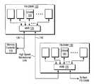
- FIG. 1illustrates one embodiment for a FB-DIMM.
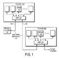
- FIG. 2Aincludes the FB-DIMMs of FIG. 1 with annotations to illustrate latencies between a memory controller and two FB-DIMMs.
- FIG. 2Billustrates latency in accessing an FB-DIMM with DRAM stacks, where each stack contains two DRAMs.
- FIG. 3is a block diagram illustrating one embodiment of a memory device that includes multiple memory core chips.
- FIG. 4is a block diagram illustrating one embodiment for partitioning a high speed DRAM device into asynchronous memory core chip and an interface chip.
- FIG. 5is a block diagram illustrating one embodiment for partitioning a memory device into a synchronous memory chip and a data interface chip.
- FIG. 6illustrates one embodiment for stacked memory chips.
- FIG. 7is a block diagram illustrating one embodiment for interfacing a memory device to a DDR2 memory bus.
- FIG. 8 ais a block diagram illustrating one embodiment for stacking memory chips on a DIMM module.
- FIG. 8 bis a block diagram illustrating one embodiment for stacking memory chips with memory sparing.
- FIG. 8 cis a block diagram illustrating operation of a working pool of stack memory.
- FIG. 8 dis a block diagram illustrating one embodiment for implementing memory sparing for stacked memory chips.
- FIG. 8 eis a block diagram illustrating one embodiment for implementing memory sparing on a per stack basis.
- FIG. 9 ais a block diagram illustrating memory mirroring in accordance with one embodiment.
- FIG. 9 bis a block diagram illustrating one embodiment for a memory device that enables memory mirroring.
- FIG. 9 cis a block diagram illustrating one embodiment for a mirrored memory system with stacks of memory.
- FIG. 9 dis a block diagram illustrating one embodiment for enabling memory mirroring simultaneously across all stacks of a DIMM.
- FIG. 9 eis a block diagram illustrating one embodiment for enabling memory mirroring on a per stack basis.
- FIG. 10 ais a block diagram illustrating a stack of memory chips with memory RAID capability during execution of a write operation.
- FIG. 10 bis a block diagram illustrating a stack of memory chips with memory RAID capability during a read operation.
- FIG. 11illustrates conventional impedance loading as a result of adding DRAMs to a high-speed memory bus.
- FIG. 12illustrates impedance loading as a result of adding DRAMs to a high-speed memory bus in accordance with one embodiment.
- FIG. 13is a block diagram illustrating one embodiment for adding low-speed memory chips using a socket.
- FIG. 14illustrates a PCB with a socket located on top of a stack.
- FIG. 15illustrates a PCB with a socket located on the opposite side from the stack.
- FIG. 16illustrates an upgrade PCB that contains one or more memory chips.
- FIG. 17is a block diagram illustrating one embodiment for stacking memory chips.
- FIG. 18is a timing diagram for implementing memory RAID using a datamask (“DM”) signal in a three chip stack composed of 8 bit wide DDR2 SDRAMS.
- DMdatamask
- FIG. 1illustrates one embodiment of a memory channel with FB-DIMMs.
- FB-DIMMs 100 and 150include DRAM chips ( 110 and 160 ) and AMBs 120 and 170 .
- a high-speed bi-directional link 135couples a memory controller 130 to FB-DIMM 100 .
- FB-DIMM 100is coupled to FB-DIMM 150 via high-speed bi-directional link 140 . Additional FB-DIMMs may be added in a similar manner.
- the FB-DIMM solutionhas some drawbacks, the two main ones being higher cost and higher latency (i.e. lower performance).
- Each AMBis expected to cost $10-$15 in volume, a substantial additional fraction of the memory module cost.
- each AMBintroduces a substantial amount of latency ( ⁇ 5 ns). Therefore, as the memory capacity of the system increases by adding more FB-DIMMs, the performance of the system degrades due to the latencies of successive AMBs.
- FIG. 2Aincludes the FB-DIMMs of FIG. 1 with annotations to illustrate latencies between a memory controller and two FB-DIMMs.
- the latency between memory controller 130 and FB-DIMM 100is the sum of t 1 and t c1 , wherein t 1 is the delay between memory channel interface of the AMB 120 and the DRAM interface of AMB 120 (i.e., the delay through AMB 120 when acting as a bridge), and t c1 is the signal propagation delay between memory controller 130 and FB-DIMM 100 .
- t 1includes the delay of the address/control signals through AMB 120 and optionally that of the data signals through AMB 120 .
- t c1includes the propagation delay of signals from the memory controller 130 to FB-DIMM 100 and optionally, that of the signals from FB-DIMM 100 to the memory controller 130 . As shown in FIG.
- the latency between memory controller 130 and FB-DIMM 150is the sum of t 2 +t 1 +t c1 +t c2 , wherein t 2 is the delay between input and output memory channel interfaces of AMB 120 (i.e. when AMB 120 is operating as a repeater) and t c2 is a signal propagation delay between FB-DIMM 100 and FB-DIMM 150 .
- t 2includes the delay of the signals from the memory controller 130 to FB-DIMM 150 through AMB 120 , and optionally that of the signals from FB-DIMM 150 to memory controller 130 through AMB 120 .
- t c2represents the propagation delay of signals from FB-DIMM 100 to FB-DIMM 150 and optionally that of signals from FB-DIMM 150 and FB-DIMM 100 .
- t 1represents the delay of the signals through an AMB chip that is operating as a bridge, which in this instance, is AMB 170 .
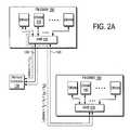
- FIG. 2Billustrates latency in accessing an FB-DIMM with DRAM stacks, where each stack contains two DRAMs.
- a “stack”comprises at least one DRAM chip.
- a “stack”comprises an interface or buffer chip with at least one DRAM chip.
- FB-DIMM 210includes three stacks of DRAMs ( 220 , 230 and 240 ) and AMB 250 accessed by memory controller 200 . As shown in FIG. 2B , the latency for accessing the stacks of DRAMs is the sum of t 1 and t c1 . It can be seen from FIGS.
- FIG. 2Bshows the case of 2 standard FB-DIMMs vs. an FB-DIMM that uses 2-DRAM stacks as an example. However, this may be extended to n standard FB-DIMMs vs. an FB-DIMM that uses n-DRAM stacks.
- Stacking high speed DRAMs on top of each otherhas its own challenges. As high speed DRAMs are stacked, their respective electrical loads or input parasitics (input capacitance, input inductance, etc.) add up, causing signal integrity and electrical loading problems and thus limiting the maximum interface speed at which a stack may operate. In addition, the use of source synchronous strobe signals introduces an added level of complexity when stacking high speed DRAMs.
- FIG. 3is a block diagram illustrating one embodiment of a memory device that includes multiple memory core chips.
- Memory device 320includes a high speed interface chip 300 and a plurality of low speed memory chips 310 stacked behind high speed interface chip 300 .
- FIG. 4is a block diagram illustrating one embodiment for partitioning a high speed DRAM device into asynchronous memory core and an interface chip.
- Memory device 400includes asynchronous memory core chip 420 interfaced to a memory channel via interface chip 410 .
- interface chip 410receives address ( 430 ), command ( 440 ) and data ( 460 ) from an external data bus, and uses address ( 435 ), command & control ( 445 and 450 ) and data ( 465 ) over an internal data bus to communicate with asynchronous memory core chip 420 .
- the address bus of a high speed DRAMtypically runs at a lower speed than the data bus.
- the address busruns at a 200 MHz speed while the data bus runs at a 400 MHz speed
- the address busruns at a 400 MHz speed while the data bus runs at an 800 MHz speed.
- High-speed DRAMsuse pre-fetching in order to support high data rates.
- a DDR2-800 deviceruns internally at a rate equivalent to 200 MHz rate except that 4n data bits are accessed from the memory core for each read or write operation, where n is the width of the external data bus.
- the 4n internal data bitsare multiplexed/de-multiplexed onto the n external data pins, which enables the external data pins to run at 4 times the internal data rate of 200 MHz.
- FIG. 5is a block diagram illustrating one embodiment for partitioning a memory device into a synchronous memory chip and a data interface chip.
- memory device 500includes synchronous memory chip 510 and a data interface chip 520 .
- Synchronous memory chip 510receives address ( 530 ) and command & clock 540 from a memory channel. It also connected with data interface chip 520 through command & control ( 550 ) and data 570 over a 4n bit wide internal data bus.
- Data interface chip 520connects to an n-bit wide external data bus 545 and a 4n-bit wide internal data bus 570 .
- an n-bit wide high speed DRAMmay be partitioned into an m*n-bit wide synchronous DRAM chip and a high-speed data interface chip that does the m*n-to-n data multiplexing/de-multiplexing, where m is the amount of pre-fetching, m>1, and m is typically an even number.
- the partitioningshould be done in such a way that: the host system sees only a single load (per DIMM in the embodiments where the memory devices are on a DIMM) on the high speed signals or pins of the memory channel or bus and the memory chips that are to be stacked on top of each other operate at a speed lower than the data rate of the memory channel or bus (i.e. the rate of the external data bus), such that stacking these chips does not affect the signal integrity.
- multiple memory chipsmay be stacked behind a single interface chip that interfaces to some or all of the signals of the memory channel. Note that this means that some or all of the I/O signals of a memory chip connect to the interface chip rather than directly to the memory channel or bus of the host system.
- the I/O signals from the multiple memory chipsmay be bussed together to the interface chip or may be connected as individual signals to the interface chip.
- the I/O signals from the multiple memory chips that are to be connected directly to the memory channel or bus of the host systemmay be bussed together or may be connected as individual signals to the external memory bus.
- One or more busesmay be used when the I/O signals are to be bussed to either the interface chip or the memory channel or bus.
- the power for the memory chipsmay be supplied by the interface chip or may come directly from the host system.
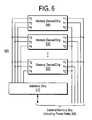
- FIG. 6illustrates one embodiment for stacked memory chips.
- Memory chips( 620 , 630 and 640 ) include inputs and/or outputs for s 1 , s 2 , s 3 , s 4 as well as v 1 and v 2 .
- the s 1 and s 2 inputs and/or outputsare coupled to external memory bus 650
- s 3 and s 4 inputs and/or outputsare coupled to interface chip 610 .
- Memory signals s 1 and s 4are examples of signals that are not bussed.
- Memory signals s 2 and s 3are examples of bussed memory signals.
- Memory power rail v 1is an example of memory power connected directly to external bus 650
- v 2is an example of memory power rail connected to interface 610 .
- the memory chips that are to be stacked on top of each othermay be stacked as dies or as individually packaged parts.
- One methodis to stack individually packaged parts since these parts may be tested and burnt-in before stacking.
- packaged partsmay be stacked on top of each other and soldered together, it is quite easy to repair a stack. To illustrate, if a part in the stack were to fail, the stack may be de-soldered and separated into individual packages, the failed chip may be replaced by a new and functional chip, and the stack may be re-assembled.
- repairing a stack as described aboveis time consuming and labor intensive.
- One way to build an effective p-chip memory stackis to use p+q memory chips and an interface chip, where the q extra memory chips (1 ⁇ q ⁇ p, typically) are spare chips, wherein p and q comprise integer values. If one or more of the p memory chips becomes damaged during assembly of the stack, they may be replaced with the spare chips.
- the post-assembly detection of a failed chipmay either be done using a tester or using built-in self test (BIST) logic in the interface chip.
- BISTbuilt-in self test
- the interface chipmay also be designed to have the ability to replace a failed chip with a spare chip such that the replacement is transparent to the host system.
- a hard erroris typically caused by broken or defective hardware such that the memory chip consistently returns incorrect results. For example, a cell in the memory array might be stuck low so that it always returns a value of “0” even when a “1” is stored in that cell.
- Hard errorsare caused by silicon defects, bad solder joints, broken connector pins, etc. Hard errors may typically be screened by rigorous testing and burn-in of DRAM chips and memory modules.
- Soft errorsare random, temporary errors that are caused when a disturbance near a memory cell alters the content of the cell. The disturbance is usually caused by cosmic particles impinging on the memory chips. Soft errors may be corrected by overwriting the bad content of the memory cell with the correct data. For DRAMs, soft errors are more prevalent than hard errors.
- ECCerror correcting code
- Computer manufacturersuse many techniques to deal with soft errors. The simplest way is to use an error correcting code (ECC), where typically 72 bits are used to store 64 bits of data. This type of code allows the detection and correction of a single-bit error, and the detection of two-bit errors. ECC does not protect against a hard failure of a DRAM chip. Computer manufacturers use a technique called Chipkill or Advanced ECC to protect against this type of chip failure. Disk manufacturers use a technique called Redundant Array of Inexpensive Disks (RAID) to deal with similar disk errors.
- RAIDRedundant Array of Inexpensive Disks
- Memory sparinginvolves the use of a spare or redundant memory bank that replaces a memory bank that exhibits an unacceptable level of soft errors.
- a memory bankmay be composed of a single DIMM or multiple DIMMs. Note that the memory bank in this discussion about advanced memory protection techniques should not be confused with the internal banks of DRAMs.
- every block of datais written to system or working memory as well as to the same location in mirrored memory but data is read back only from working memory. If a bank in the working memory exhibits an unacceptable level of errors during read back, the working memory will be replaced by the mirrored memory.
- RAIDis a well-known set of techniques used by the disk industry to protect against disk errors. Similar RAID techniques may be applied to memory technology to protect against memory errors. Memory RAID is similar in concept to RAID 3 or RAID 4 used in disk technology. In memory RAID a block of data (typically some integer number of cachelines) is written to two or more memory banks while the parity for that block is stored in a dedicated parity bank. If any of the banks were to fail, the block of data may be re-created with the data from the remaining banks and the parity data.
- a DIMM or FB-DIMMmay be built using memory stacks instead of individual DRAMs.
- a standard FB-DIMMmight contain nine, 18, or more DDR2 SDRAM chips.
- An FB-DIMMmay contain nine 18, or more DDR2 stacks, wherein each stack contains a DDR2 SDRAM interface chip and one or more low speed memory chips stacked on top of it (i.e. electrically behind the interface chip—the interface chip is electrically between the memory chips and the external memory bus).
- a standard DDR2 DIMMmay contain nine 18 or more DDR2 SDRAM chips.
- a DDR2 DIMMmay instead contain nine 18, or more DDR2 stacks, wherein each stack contains a DDR2 SDRAM interface chip and one or more low speed memory chips stacked on top of it.
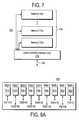
- An example of a DDR2 stack built according to one embodimentis shown in FIG. 7 .
- FIG. 7is a block diagram illustrating one embodiment for interfacing a memory device to a DDR2 memory bus.
- memory device 700comprises memory chips 720 coupled to DDR2 SDRAM interface chip 710 .
- DDR2 SDRAM interface chip 710interfaces memory chips 720 to external DDR2 memory bus 730 .
- an effective p-chip memory stackmay be built with p+q memory chips and an interface chip, where the q chips may be used as spares, and p and q are integer values.
- the p+q chipsmay be separated into two pools of chips: a working pool of p chips and a spare pool of q chips.
- a chip in the working poolmay be replaced by a chip from the spare pool.
- the replacement of a failed working chip by a spare chipmay be triggered, for example, by the detection of a multi-bit failure in a working chip, or when the number of errors in the data read back from a working chip crosses a pre-defined or programmable error threshold.
- ECCis typically implemented across the entire 64 data bits in the memory channel and optionally, across a plurality of memory channels, the detection of single-bit or multi-bit errors in the data read back is only done by the memory controller (or the AMB in the case of an FB-DIMM).
- the memory controller(or AMB) may be designed to keep a running count of errors in the data read back from each DIMM. If this running count of errors were to exceed a certain pre-defined or programmed threshold, then the memory controller may communicate to the interface chip to replace the chip in the working pool that is generating the errors with a chip from the spare pool.
- each DDR2 stackconsists of five chips, four of which are assigned to the working pool and the fifth chip is assigned to the spare pool.
- the first chip in the working poolcorresponds to address range [N-1:0]
- the second chip in the working poolcorresponds to address range [2N-1:N]
- the third chip in the working poolcorresponds to address range [3N-1:2N]
- the fourth chip in the working poolcorresponds to address range [4N-1:3N], where “N” is an integer value.
- the memory controllermay be designed to keep track of the errors in the data from the address ranges [4N-1:3N], [3N-1:2N], [2N-1:N], and [N-1:0]. If, say, the errors in the data in the address range [3N-1:2N] exceeded the pre-defined threshold, then the memory controller may instruct the interface chip in the stack to replace the third chip in the working pool with the spare chip in the stack. This replacement may either be done simultaneously in all the nine stacks in the DIMM or may be done on a per-stack basis. Assume that the errors in the data from the address range [3N-1:2N] are confined to data bits [7:0] from the DIMM.
- the third chip in all the stackswill be replaced by the spare chip in the respective stacks.
- the latter caseonly the third chip in stack 0 (the LSB stack) will be replaced by the spare chip in that stack.
- the latter caseis more flexible since it compensates for or tolerates one failing chip in each stack (which need not be the same chip in all the stacks), whereas the former case compensates for or tolerates one failing chip over all the stacks in the DIMM. So, in the latter case, for an effective p-chip stack built with p+q memory chips, up to q chips may fail per stack and be replaced with spare chips.
- the memory controller(or AMB) may trigger the memory sparing operation (i.e. replacing a failing working chip with a spare chip) by communicating with the interface chips either through in-band signaling or through sideband signaling.
- a System Management Bus (SMBus)is an example of sideband signaling.
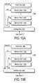
- FIGS. 8 a - 8 eEmbodiments for memory sparing within a memory stack configured in accordance with some embodiments are shown in FIGS. 8 a - 8 e.
- FIG. 8 ais a block diagram illustrating one embodiment for stacking memory chips on a DIMM module.
- memory module 800includes nine stacks ( 810 , 820 , 830 , 840 , 850 , 860 , 870 , 880 and 890 ). Each stack comprises at least two memory chips.
- memory module 800is configured to work in accordance with DDR2 specifications.
- FIG. 8 bis a block diagram illustrating one embodiment for stacking memory chips with memory sparing.
- memory device 875includes memory chips ( 885 , 886 , 888 and 892 ) stacked to form the working memory pool.
- the memory chipsare each assigned a range of addresses as shown in FIG. 8 b .
- Memory device 875also includes spare memory chip 895 that forms the spare memory pool.
- the spare memory poolmay comprise any number of memory chips.
- FIG. 8 cis a block diagram illustrating operation of a working memory pool.
- memory module 812includes a plurality of integrated circuit memory stacks ( 814 , 815 , 816 , 817 , 818 , 819 , 821 , 822 and 823 ).
- each stackcontains a working memory pool 825 and a spare memory chip 855 .
- FIG. 8 dis a block diagram illustrating one embodiment for implementing memory sparing for stacked memory chips.
- memory module 824also includes a plurality of integrated circuit memory stacks ( 826 , 827 , 828 , 829 , 831 , 832 , 833 , 834 and 835 ).
- memory sparingmay be enabled if data errors occur in one or more memory chips (i.e., occur in an address range).
- data errors exceeding a predetermined thresholdhave occurred in DQ[7:0] in the address range [3N-1:2N].
- the failing chipis replaced simultaneously in all of the stacks of the DIMM. Specifically, for this example, failing chip 857 is replaced by spare chip 855 in all memory stacks of the DIMM.
- FIG. 8 eis a block diagram illustrating one embodiment for implementing memory sparing on a per stack basis.
- memory module 836also includes a plurality of integrated circuit memory stacks ( 837 , 838 , 839 , 841 , 842 , 843 , 844 , 846 and 847 ).
- Each stackis apportioned into the working memory pool and a spare memory pool (e.g., spare chip 861 ).
- memory chip chip 863failed in stack 847 .
- the spare chip in stack 847replaces the failing chip, and all other stacks continue to operate using the working pool.
- Memory mirroringcan be implemented by dividing the p+q chips in each stack into two equally sized sections—the working section and the mirrored section. Each data that is written to memory by the memory controller is stored in the same location in the working section and in the mirrored section.
- the interface chipreads only the appropriate location in the working section and returns the data to the memory controller. If the memory controller detects that the data returned had a multi-bit error, for example, or if the cumulative errors in the read data exceeded a pre-defined or programmed threshold, the memory controller can be designed to tell the interface chip (by means of in-band or sideband signaling) to stop using the working section and instead treat the mirrored section as the working section.
- this replacementcan either be done across all the stacks in the DIMM or can be done on a per-stack basis.
- the latter caseis more flexible since it can compensate for or tolerate one failing chip in each stack whereas the former case can compensate for or tolerate one failing chip over all the stacks in the DIMM.
- FIGS. 9 a - 9 eEmbodiments for memory mirroring within a memory stack are shown in FIGS. 9 a - 9 e.
- FIG. 9 ais a block diagram illustrating memory mirroring in accordance with one embodiment.
- a memory device 900includes interface chip 910 that interfaces memory to an external memory bus.
- the memoryis apportioned into a working memory section 920 and a mirrored memory section 930 .
- write operationsoccur in both the working memory section 920 and the mirrored memory section 930 .
- read operationsare only conducted from the working memory section 920 .
- FIG. 9 bis a block diagram illustrating one embodiment for a memory device that enables memory mirroring.
- memory device 900uses mirrored memory section 930 as working memory due to a threshold of errors that occurred in the working memory 920 .
- working memory section 920is labeled as the unusable working memory section.
- interface chip 910executes write operations to mirrored memory section 930 and optionally to the unusable working memory section 920 .
- readsoccur from mirrored memory section 930 .
- FIG. 9 cis a block diagram illustrating one embodiment for a mirrored memory system with integrated circuit memory stacks.
- memory module 915includes a plurality of integrated circuit memory stacks ( 902 , 903 , 904 , 905 , 906 , 907 , 908 , 909 and 912 ).
- each stackis apportioned into a working memory section 953 , and labeled “W” in FIG. 9 c , as well as a mirrored memory section 951 , labeled “M” in FIG. 9 c .
- the working memory sectionis accessed (i.e., mirrored memory is not enabled).
- FIG. 9 dis a block diagram illustrating one embodiment for enabling memory mirroring simultaneously across all stacks of a DIMM.
- memory module 925also includes a plurality of integrated circuit memory stacks ( 921 , 922 , 923 , 924 , 926 , 927 , 928 , 929 and 931 ) apportioned into a mirrored memory section 956 and a working memory section 958 .
- a mirrored memory section 956and a working memory section 958 .
- all chips in the mirrored memory section for each stack in the DIMMare used as the working memory.
- FIG. 9 eis a block diagram illustrating one embodiment for enabling memory mirroring on a per stack basis.
- memory module 935includes a plurality of integrated circuit memory stacks ( 941 , 942 , 943 , 944 , 945 , 946 , 947 , 948 and 949 ) apportioned into a mirrored section 961 (labeled “M”) and a working memory section 963 (labeled “W”).
- mirrored memory from the corresponding stackis replaced with working memory. For example, if data errors occurred in DQ[7:0] and exceed a threshold, then mirrored memory section 961 (labeled “Mu”) replaces working memory section 963 (labeled “uW”) for stack 949 only.
- memory RAID within a (p+1)-chip stackmay be implemented by storing data across p chips and storing the parity (i.e. the error correction code or information) in a separate chip (i.e. the parity chip). So, when a block of data is written to the stack, the block is broken up into p equal sized portions and each portion of data is written to a separate chip in the stack. That is, the data is “striped” across p chips in the stack.
- the memory controllerwrites data block A to the memory stack.
- the interface chipsplits this data block into p equal sized portions (A 1 , A 2 , A 3 , . . . , Ad and writes A 1 to the first chip in the stack, A 2 to the second chip, A 3 to the third chip, and so on, till A p is written to the p th chip in the stack.
- the parity information for the entire data block Ais computed by the interface chip and stored in the parity chip.
- the interface chipreads A 1 , A 2 , A 3 , . . . , A p from the first, second, third, . . .
- the memory controllermay instruct the interface chip to re-create the correct data using the parity information and the correct portions of the data block A.
- Embodiments for memory RAID within a memory stackare shown in FIGS. 10 a and 10 b.
- FIG. 10 ais a block diagram illustrating a stack of memory chips with memory RAID capability during execution of a write operation.
- Memory device 1000includes an interface chip 1010 to interface “p+1” memory chips ( 1015 , 1020 , 1025 , and 1030 ) to an external memory bus.
- FIG. 10 ashows a write operation of a data block “A”, wherein data for data block “A” is written into memory chips as follows.
- AAp . . . A2, A1;
- Parity[A](Ap)n . . . n(A2), n(A1),
- nis the bitwise exclusive OR operator
- FIG. 10 bis a block diagram illustrating a stack of memory chips with memory RAID capability during a read operation.
- Memory device 1040includes interface chip 1050 , “p” memory chips ( 1060 , 1070 and 1080 ) and a parity memory chip 1090 .
- data block “A”consists of A1, A2, . . . Ap and Parity[A], and is read from the respective memory memory chips as shown in FIG. 10 b.
- the memory controllermay implement error correction across the data from all the memory stacks on a DIMM, and optionally, across multiple DIMMs.
- the bits stored in the extra chipmay have alternative functions than parity.
- the extra storage or hidden bit fieldmay be used to tag a cacheline with the address of associated cachelines.
- the memory controllerfetched cacheline A, it also then fetched cacheline B (where B is a random address).
- the memory controllercan then write back cacheline A with the address of cacheline B in the hidden bit field.
- the next time the memory controller reads cacheline Ait will also read the data in the hidden bit field and pre-fetch cacheline B.
- metadata or cache tags or prefetch informationmay be stored in the hidden bit field.
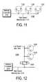
- FIG. 11illustrates conventional impedance loading as a result of adding DRAMs to a high-speed memory bus.
- memory controller 1110accesses memory on high-speed bus 1115 .
- the load of a conventional DRAM on high-speed memory bus 1115is illustrated in FIG. 11 ( 1120 ).
- memory chipsare added to the high-speed bus 1115 , and consequently additional loads ( 1125 and 1130 ) are also added to the high-speed memory bus 1115 .
- a single high speed interface chipcan be connected to some or all of the lines of a memory bus, thus providing a known and fixed load on the memory bus. Since the other side of the interface chip runs at a lower speed, multiple low speed memory chips can be connected to (the low speed side of) the interface chip without sacrificing performance, thus providing the ability to upgrade memory. In effect, the electrical loading of additional memory chips has been shifted from a high speed bus (which is the case today with conventional high speed DRAMs) to a low speed bus. Adding additional electrical loads on a low speed bus is always a much easier problem to solve than that of adding additional electrical loads on a high speed bus.
- FIG. 12illustrates impedance loading as a result of adding DRAMs to a high-speed memory bus in accordance with one embodiment.
- memory controller 1210accesses a high-speed interface chip 1200 on high-speed memory bus 1215 .
- the load 1220 from the high-speed interface chipis shown in FIG. 12 .
- a low speed bus 1240couples to high-speed interface chip 1200 .
- the loads of the memory chips ( 1230 and 1225 )are applied to low speed bus 1240 . As a result, additional loads are not added to high-speed memory bus 1215 .
- the number of low speed memory chips that are connected to the interface chipmay either be fixed at the time of the manufacture of the memory stack or may be changed after the manufacture.
- the ability to upgrade and add extra memory capacity after the manufacture of the memory stackis particularly useful in markets such as desktop PCs where the user may not have a clear understanding of the total system memory capacity that is needed by the intended applications.
- This ability to add additional memory capacitywill become very critical when the PC industry adopts DDR3 memories in several major market segments such as desktops and mobile. The reason is that at DDR3 speeds, it is expected that only one DIMM can be supported per memory channel. This means that there is no easy way for the end user to add additional memory to the system after the system has been built and shipped.
- a socketmay be used to add at least one low speed memory chip.
- the socketcan be on the same side of the printed circuit board (PCB) as the memory stack but be adjacent to the memory stack, wherein a memory stack may consist of at least one high speed interface chip or at least one high speed interface chip and at least one low speed memory chip.
- FIG. 13is a block diagram illustrating one embodiment for adding low speed memory chips using a socket.
- a printed circuit board (PCB) 1300such as a DIMM, includes one or more stacks of high speed interface chips.
- the stacksalso include low-speed memory chips. As shown in FIG.
- one or more socketsare mounted on the PCB 1300 adjacent to the stacks 1320 .
- Low-speed memory chipsmay be added to the sockets to increase the memory capacity of the PCB 1300 .
- the sockets 1310are located on the same side of the PCB 1300 as stacks 1320 .
- the socket for additional low speed memory chipscan be designed to be on the same side of the PCB as the memory stack and sit on top of the memory stack, as shown in FIG. 14 .
- FIG. 14illustrates a PCB with a socket located on top of a stack.
- PCB 1400includes a plurality of stacks ( 1420 ).
- a stackcontains a high speed interface chip and optionally, one or more low speed memory chips.
- a socket ( 1410 )sits on top of one or more stacks.
- Memory chipsare placed in the socket(s) ( 1410 ) to add memory capacity to the PCB (e.g., DIMM).
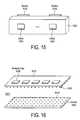
- the socket for the additional low speed memory chipscan be designed to be on the opposite side of the PCB from the memory stack, as shown in FIG. 15 .
- FIG. 15illustrates a PCB with a socket located on the opposite side from the stack.
- PCB 1500such as a DIMM, comprises one or more stacks ( 1520 ) containing high speed interface chips, and optionally, one or more low speed memory chips.
- one or more sockets ( 1510 )are mounted on the opposite side of the PCB from the stack as shown in FIG. 15 .
- the low speed memory chipsmay be added to the memory stacks one at a time. That is, each stack may have an associated socket. In this case, adding additional capacity to the memory system would involve adding one or more low speed memory chips to each stack in a memory rank (a rank denotes all the memory chips or stacks that respond to a memory access; i.e.
- socketscan be used.
- the socketmay be a female type and the PCB with the upgrade memory chips may have associated male pins.
- FIG. 16illustrates an upgrade PCB that contains one or more memory chips.
- an upgrade PCB 1610includes one or more memory chips ( 1620 ).
- PCB 1610includes male socket pins 1630 .
- a female receptacle socket 1650 on a DIMM PCBmates with the male socket pins 1630 to upgrade the memory capacity to include additional memory chips ( 1620 ).
- Another approachwould be to use a male type socket and an upgrade PCB with associated female receptacles.
- DRAMsuse source synchronous strobe signals as the timing reference for bi-directional transfer of data.
- a dedicated strobe signalis associated with the four data signals of the DRAM.
- a dedicated strobe signalis associated with the eight data signals.
- a dedicated strobe signalis associated with each set of eight data signals.
- Most memory controllersare designed to accommodate a dedicated strobe signal for every four or eight data lines in the memory channel or bus.
- a buffer chipis located between the external memory channel and the DRAM chips and buffers at least one of the address, control, and data signals to and from the DRAM chips.
- one buffer chipmay be used per stack. In other implementations, more than one buffer chip may be used per stack. In yet other implementations, one buffer chip may be used for a plurality of stacks.
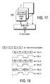
- FIG. 17is a block diagram illustrating one embodiment for stacking memory chips.
- buffer chip 1810is coupled to a host system, typically to the memory controller of the system.
- Memory device 1800contains at least two high-speed memory chips 1820 (e.g., DRAMs such as DDR2 SDRAMs) stacked behind the buffer chip 1810 (e.g., the high-speed memory chips 1820 are accessed by buffer chip 1810 ).
- DRAMssuch as DDR2 SDRAMs
- FIG. 17is similar to that described previously and illustrated in FIG. 3 .
- the main differenceis that in the scheme illustrated in FIG. 3 , multiple low speed memory chips were stacked on top of a high speed interface chip.
- the high speed interface chippresented an industry-standard interface (such as DDR SDRAM or DDR2 SDRAM) to the host system while the interface between the high speed interface chip and the low speed memory chips may be non-standard (i.e. proprietary) or may conform to an industry standard.
- the scheme illustrated in FIG. 17stacks multiple high speed, off-the-shelf DRAMs on top of a high speed buffer chip.
- the buffer chipmay or may not perform protocol translation (i.e. the buffer chip may present an industry-standard interface such as DDR2 to both the external memory channel and to the high speed DRAM chips) and may simply isolate the electrical loads represented by the memory chips (i.e. the input parasitics of the memory chips) from the memory channel.
- the buffer chipmay perform protocol translations.
- the buffer chipmay provide translation from DDR3 to DDR2.
- multiple DDR2 SDRAM chipsmight appear to the host system as one or more DDR3 SDRAM chips.
- the buffer chipmay also translate from one version of a protocol to another version of the same protocol.
- the buffer chipmay translate from one set of DDR2 parameters to a different set of DDR2 parameters.
- the buffer chipmight, for example, make one or more DDR2 chips of one type (e.g. 4-4-4 DDR2 SDRAM) appear to the host system as one of more DDR2 chips of a different type (e.g. 6-6-6 DDR2 SDRAM).
- a buffer chipmay be shared by more than one stack.
- the buffer chipmay be external to the stack rather than being part of the stack. More than one buffer chip may also be associated with a stack.
- Using a buffer chip to isolate the electrical loads of the high speed DRAMs from the memory channelallows us to stack multiple (typically between two and eight) memory chips on top of a buffer chip.
- all the memory chips in a stackmay connect to the same address bus.
- a plurality of address busesmay connect to the memory chips in a stack, wherein each address bus connects to at least one memory chip in the stack.
- the data and strobe signals of all the memory chips in a stackmay connect to the same data bus in one embodiment, while in another embodiment, multiple data buses may connect to the data and strobe signals of the memory chips in a stack, wherein each memory chip connects to only one data bus and each data bus connects to at least one memory chip in the stack.
- the simulationmay refer to any simulating, emulating, disguising, and/or the like that results in at least one aspect (e.g. a number in this embodiment, etc.) of the DRAMs appearing different to the system.
- the simulationmay be electrical in nature, logical in nature, and/or performed in any other desired manner. For instance, in the context of electrical simulation, a number of pins, wires, signals, etc. may be simulated, while, in the context of logical simulation, a particular function may be simulated.
- the second numbermay be more or less than the first number. Still yet, in the latter case, the second number may be one, such that a single DRAM is simulated.
- Different optional embodiments which may employ various aspects of the present embodimentwill be set forth hereinafter.
- the buffer chipmay be operable to interface the DRAMs and the system for simulating at least one DRAM with at least one aspect that is different from at least one aspect of at least one of the plurality of the DRAMs.
- such aspectmay include a signal, a capacity, a timing, a logical interface, etc.
- such signalmay include an address signal, control signal, data signal, and/or any other signal, for that matter.
- a number of the aforementioned signalsmay be simulated to appear as fewer or more signals, or even simulated to correspond to a different type.
- multiple signalsmay be combined to simulate another signal. Even still, a length of time in which a signal is asserted may be simulated to be different.
- the buffer chipmay be operable for simulating at least one DRAM with a first memory capacity that is greater than (or less than) a second memory capacity of at least one of the DRAMs.
- the timingmay possibly relate to a latency (e.g. time delay, etc.).
- a latencye.g. time delay, etc.
- such latencymay include a column address strobe (CAS) latency (tCAS), which refers to a latency associated with accessing a column of data.
- the latencymay include a row address strobe (RAS) to CAS latency (tRCD), which refers to a latency required between RAS and CAS.
- RASrow address strobe
- tRCDrow address strobe
- the latencymay include a row precharge latency (tRP), which refers a latency required to terminate access to an open row.
- the latencymay include an active to precharge latency (tRAS), which refers to a latency required to access a certain row of data between a data request and a precharge command.
- tRASactive to precharge latency
- the buffer chipmay be operable for simulating at least one DRAM with a first latency that is longer (or shorter) than a second latency of at least one of the DRAMs.
- a buffer chipmay be operable to receive a signal from the system and communicate the signal to at least one of the DRAMs after a delay.
- the signalmay refer to an address signal, a command signal (e.g. activate command signal, precharge command signal, a write signal, etc.) data signal, or any other signal for that matter.
- a command signale.g. activate command signal, precharge command signal, a write signal, etc.
- delaymay be fixed or variable.
- the delaymay include a cumulative delay associated with any one or more of the aforementioned signals. Even still, the delay may time shift the signal forward and/or back in time (with respect to other signals). Of course, such forward and backward time shift may or may not be equal in magnitude. In one embodiment, this time shifting may be accomplished by utilizing a plurality of delay functions which each apply a different delay to a different signal.
- the aforementioned buffer chipmay include a register, an advanced memory buffer (AMB), a component positioned on at least one DIMM, a memory controller, etc.
- AMBadvanced memory buffer
- Such registermay, in various embodiments, include a Joint Electron Device Engineering Council (JEDEC) register, a JEDEC register including one or more functions set forth herein, a register with forwarding, storing, and/or buffering capabilities, etc.
- JEDECJoint Electron Device Engineering Council
- the simulated DRAM circuitmay be desirable to determine whether the simulated DRAM circuit behaves according to a desired DRAM standard or other design specification.
- a behavior of many DRAM circuitsis specified by the JEDEC standards and it may be desirable, in some embodiments, to exactly simulate a particular JEDEC standard DRAM.
- the JEDEC standarddefines commands that a DRAM circuit must accept and the behavior of the DRAM circuit as a result of such commands.
- the JEDEC specification for a DDR2 DRAMis known as JESD79-2B.
- the following algorithmmay be used. Such algorithm checks, using a set of software verification tools for formal verification of logic, that protocol behavior of the simulated DRAM circuit is the same as a desired standard or other design specification. This formal verification is quite feasible because the DRAM protocol described in a DRAM standard is typically limited to a few protocol commands (e.g. approximately 15 protocol commands in the case of the JEDEC DDR2 specification, for example).
- Examples of the aforementioned software verification toolsinclude MAGELLAN supplied by SYNOPSYS, or other software verification tools, such as INCISIVE supplied by CADENCE, verification tools supplied by JASPER, VERIX supplied by REAL INTENT, 0-IN supplied by MENTOR CORPORATION, and others. These software verification tools use written assertions that correspond to the rules established by the DRAM protocol and specification. These written assertions are further included in the code that forms the logic description for the buffer chip. By writing assertions that correspond to the desired behavior of the simulated DRAM circuit, a proof may be constructed that determines whether the desired design requirements are met. In this way, one may test various embodiments for compliance with a standard, multiple standards, or other design specification.
- an assertionmay be written that no two DRAM control signals are allowed to be issued to an address, control and clock bus at the same time.
- the aforementioned algorithmmay allow a designer to prove that the simulated DRAM circuit exactly meets the required standard or other design specification. If, for example, an address mapping that uses a common bus for data and a common bus for address results in a control and clock bus that does not meet a required specification, alternative designs for the buffer chip with other bus arrangements or alternative designs for the interconnect between the buffer chip and other components may be used and tested for compliance with the desired standard or other design specification.
- the buffer chipmay be designed to have the same footprint (or pin out) as an industry-standard DRAM (e.g. a DDR2 SDRAM footprint).
- the high speed DRAM chips that are stacked on top of the buffer chipmay either have an industry-standard pin out or can have a non-standard pin out. This allows us to use a standard DIMM PCB since each stack has the same footprint as a single industry-standard DRAM chip.
- Several companieshave developed proprietary ways to stack multiple DRAMs on top of each other (e.g. ⁇ Z Ball Stack from Tessera, Inc., High Performance Stakpak from Staktek Holdings, Inc.).
- the disclosed techniques of stacking multiple memory chips behind either a buffer chip ( FIG. 18 ) or a high speed interface chip ( FIG. 3 )is compatible with all the different ways of stacking memory chips. It does not require any particular stacking technique.
- a double sided DIMMi.e. a DIMM that has memory chips on both sides of the PCB
- a single sided DIMMis electrically worse than a single sided DIMM, especially if the high speed data and strobe signals have to be routed to two DRAMs, one on each side of the board.
- a T topologyis typically worse from a signal integrity perspective than a point-to-point topology.
- Rambus used mirror packages on double sided Rambus In-line Memory Modules (RIMMs)so that the high speed signals had a point-to-point topology rather than a T topology.
- the buffer chipmay be designed with an industry-standard DRAM pin out and a mirrored pin out.
- the DRAM chips that are stacked behind the buffer chipmay have a common industry-standard pin out, irrespective of whether the buffer chip has an industry-standard pin out or a mirrored pin out.
- Thisallows us to build double sided DIMMs that are both high speed and high capacity by using mirrored packages and stacking respectively, while still using off-the-shelf DRAM chips.
- thisrequires the use of a non-standard DIMM PCB since the standard DIMM PCBs are all designed to accommodate standard (i.e. non-mirrored) DRAM packages on both sides of the PCB.
- the buffer chipmay be designed not only to isolate the electrical loads of the stacked memory chips from the memory channel but also have the ability to provide redundancy features such as memory sparing, memory mirroring, and memory RAID.
- redundancy featuressuch as memory sparing, memory mirroring, and memory RAID.
- Thisallows us to build high density DIMMs that not only have the same footprint (i.e. pin compatible) as industry-standard memory modules but also provide a full suite of redundancy features. This capability is important for key segments of the server market such as the blade server segment and the 1 U rack server segment, where the number of DIMM slots (or connectors) is constrained by the small form factor of the server motherboard. Many analysts have predicted that these will be the fastest growing segments in the server market.
- Memory sparingmay be implemented with one or more stacks of p+q high speed memory chips and a buffer chip.
- the p memory chips of each stackare assigned to the working pool and are available to system resources such as the operating system (OS) and application software.
- OSoperating system
- the memory controlleror optionally the AMB detects that one of the memory chips in the stack's working pool has, for example, generated an uncorrectable multi-bit error or has generated correctable errors that exceeded a pre-defined threshold, it may choose to replace the faulty chip with one of the q chips that have been placed in the spare pool.
- the memory controllermay choose to do the sparing across all the stacks in a rank even though only one working chip in one specific stack triggered the error condition, or may choose to confine the sparing operation to only the specific stack that triggered the error condition.
- the former methodis simpler to implement from the memory controller's perspective while the latter method is more fault-tolerant.
- Memory sparingwas illustrated in FIG. 8 for stacks built with a high speed interface chip and multiple low speed DRAMs. The same method is applicable to stacks built with high speed, off-the-shelf DRAMs and a buffer chip.
- the buffer chipmay not be part of the stack.
- a buffer chipmay be used with a plurality of stacks of memory chips or a plurality of buffer chips may be used by a single stack of memory chips.
- Memory mirroringcan be implemented by dividing the high speed memory chips in a stack into two equal sets—a working set and a mirrored set.
- the buffer chipWhen the memory controller writes data to the memory, the buffer chip writes the data to the same location in both the working set and the mirrored set. During reads, the buffer chip returns the data from the working set. If the returned data had an uncorrectable error condition or if the cumulative correctable errors in the returned data exceeded a pre-defined threshold, the memory controller may instruct the buffer chip to henceforth return data (on memory reads) from the mirrored set until the error condition in the working set has been rectified. The buffer chip may continue to send writes to both the working set and the mirrored set or may confine it to just the mirrored set.
- the memory mirroring operationmay be triggered simultaneously on all the memory stacks in a rank or may be done on a per-stack basis as and when necessary.
- the former methodis easier to implement while the latter method provides more fault tolerance.
- Memory mirroringwas illustrated in FIG. 9 for stacks built with a high speed interface chip and multiple low speed memory chips. The same method is applicable to stacks built with high speed, off-the-shelf DRAMs and a buffer chip.
- the buffer chipmay not be part of the stack.
- a buffer chipmay be used with a plurality of stacks of memory chips or a plurality of buffer chips may be used by a single stack of memory chips.
- the switch from the working set to the mirrored setmay be triggered by the memory controller (or AMB) sending an in-band or sideband signal to the buffers in the respective stacks.
- logicmay be added to the buffers so that the buffers themselves have the ability to switch from the working set to the mirrored set.
- some of the server memory controller hubs (MCH) from Intelwill read a memory location for a second time if the MCH detects an uncorrectable error on the first read of that memory location.
- the buffer chipmay be designed to keep track of the addresses of the last m reads and to compare the address of the current read with the stored m addresses.
- the buffer chipmay now read the contents of the memory location from the mirrored set since it knows that the contents in the corresponding location in the working set had an error.
- the buffer chipmay also be designed to keep track of the number of such events (i.e. a second read to a location due to an uncorrectable error) over some period of time. If the number of these events exceeded a certain threshold within a sliding time window, then the buffer chip may permanently switch to the mirrored set and notify an external device that the working set was being disabled.
- DDR2 SDRAMshave a minimum burst length of four
- a single read or write operationinvolves transferring four bytes of data between the memory controller and a stack. This means that the memory controller must transfer a minimum of 32 bytes of data to a memory rank (four bytes per stack*eight stacks) for each read or write operation.
- Modern CPUstypically use a 64-byte cacheline as the basic unit of data transfer to and from the system memory. This implies that eight bytes of data may be transferred between the memory controller and each stack for a read or write operation.
- the buffer chipmay be designed such that it writes the first four bytes (say, bytes Z0, Z1, Z2, and Z3) to the specified memory locations (say, addresses x1, x2, x3, and x4) in chip A and writes the second four bytes (say, bytes Z4, Z5, Z6, and Z7) to the same locations (i.e. addresses x1, x2, x3, and x4) in chip B.
- the buffer chipmay also be designed to store the parity information corresponding to these eight bytes in the same locations in chip C.
- the buffer chipwill read locations x1, x2, x3, and x4 in both chips A and B and will return bytes Z0, Z1, Z2, and Z3 from chip A and then bytes Z4, Z5, Z6, and Z7 from chip B.
- the memory controllerdetected a multi-bit error in byte Z1.
- some of the Intel server MCHswill re-read the address location when they detect an uncorrectable error in the data that was returned in response to the initial read command. So, when the memory controller re-reads the address location corresponding to byte Z1, the buffer chip may be designed to detect the second read and return P [1,5] ⁇ Z5 rather than Z1 since it knows that the memory controller detected an uncorrectable error in Z1.
- the buffer chipmay be designed to look at the appropriate column addresses to determine which byte corresponds to the uncorrectable error. For example, say that byte Z1 corresponds to the uncorrectable error and that the memory controller requests that the stack send the eight bytes (Z0 through Z7) back to the controller starting with byte Z1. In other words, the memory controller asks the stack to send the eight bytes back in the following order: Z1, Z2, Z3, Z0, Z5, Z6, Z7, and Z4 (i.e.
- the buffer chipmay be designed to recognize that this indicates that byte Z1 corresponds to the uncorrectable error and return P [1,5] ⁇ Z5, Z2, Z3, Z0, Z5, Z6, Z7, and Z4. Alternately, the buffer chip may be designed to return P [1,5] ⁇ Z5, P [2,6] ⁇ Z6, P [3,7] ⁇ Z7, P [0,4] ⁇ Z4, Z5, Z6, Z7, and Z4 if it is desired to correct not only an uncorrectable error in any given byte but also the case where an entire chip (in this case, chip A) fails.
- the memory controllerIf, on the other hand, the memory controller reads the entire cacheline in the same order both during a normal read operation and during a second read caused by an uncorrectable error, then the controller has to indicate to the buffer chip which byte or chip corresponds to the uncorrectable error either through an in-band signal or through a sideband signal before or during the time it performs the second read.
- the memory controllerdoes a 64-byte cacheline read or write in two separate bursts of length 4 (rather than a single burst of length 8 ). This may also be the case when an I/O device initiates the memory access. This may also be the case if the 64-byte cacheline is stored in parallel in two DIMMs. In such a case, the memory RAID implementation might require the use of the DM (Data Mask) signal.
- DMData Mask
- the buffer chipmay be designed to use the DM signal to steer two of the four bytes in a burst to chip A and steer the other two bytes in a burst to chip B. This concept is best illustrated by the example below.
- the stack in this exampleis composed of three 8-bit DDR2 SDRAMs (chips A, B, and C) and a buffer chip.
- the buffer chipmay be designed to generate a write command to locations x1, x2, x3, and x4 on all the three chips A, B, and C, and perform the following actions:
- FIG. 18is a timing diagram for implementing memory RAID using a datamask (DM) signal in a three chip stack composed of 8 bit wide DDR2 SDRAMS.
- the first signal of the timing diagram of FIG. 18represents data sent to the stack from the host system.
- the second and third signals, labeled DQ_A and DM_Arepresent the data and data mask signals sent by the buffer chip to chip A during a write operation to chip A.
- signals DQ_B and DM_Brepresent signals sent by the buffer chip to chip B during a write operation to chip B
- signals DQ_C and DM_Crepresent signals sent by the buffer chip to chip C during a write operation to chip C.
- the buffer chipwill read locations x1, x2, x3, and x4 from both chips A and B, select the appropriate two bytes from the four bytes returned by each chip, re-construct the original data, and send it back to the memory controller.
- the data striping across the two chipsmay be done in other ways. For example, bytes Z0 and Z1 may be written to chip A and bytes Z2 and Z3 may be written to chip B. Also, this concept may be extended to stacks that are built with a different number of chips.
- a 4-byte burst to a stackmay be striped across four chips by writing one byte to each chip and using the DM signal to mask the remaining three writes in the burst.
- the parity informationmay be stored in the fifth chip, again using the associated DM signal.
- the buffer chipmay be designed to re-construct the bad data using the data in the other chips as well as the parity information.
- the buffer chipmay perform this operation either when explicitly instructed to do so by the memory controller or by monitoring the read requests sent by the memory controller and detecting multiple reads to the same address within some period of time, or by some other means.
- the memory read latency for the case where the buffer chip has to re-construct the bad datamay most likely be higher than the normal read latency. This may be accommodated in multiple ways. Say that the normal read latency is 4 clock cycles while the read latency when the buffer chip has to re-create the bad data is 5 clock cycles. The memory controller may simply choose to use 5 clock cycles as the read latency for all read operations. Alternately, the controller may default to 4 clock cycles for all normal read operations but switch to 5 clock cycles when the buffer chip has to re-create the data. Another option would be for the buffer chip to stall the memory controller when it has to re-create some part of the data. These and other methods fall within the scope of this disclosure.
- memory RAIDusing a combination of memory chips and a buffer chip in a stack. This provides us with the ability to correct multi-bit errors either within a single memory chip or across multiple memory chips in a rank.
- chip DBy adding a fourth chip (chip D) to the stack, we can create an additional level of redundancy. Say that chip B has either failed or is generating an unacceptable level of uncorrectable errors.
- the buffer chip in the stackmay re-construct the data in chip B using the data in chip A and the parity information in chip C in the same manner that is used in well-known disk RAID systems. Obviously, the performance of the memory system may be degraded (due to the possibly higher latency associated with re-creating the data in chip B) until chip B is effectively replaced. However, since we have an unused memory chip in the stack (chip D), we may substitute it for chip B until the next maintenance operation.
- the buffer chipmay be designed to re-create the data in chip B (using the data in chip A and the parity information in chip C) and write it to chip D. Once this is completed, chip B may be discarded (i.e. no longer used by the buffer chip).
- the re-creation of the data in chip B and the transfer of the re-created data to chip Dmay be made to run in the background (i.e. during the cycles when the rank containing chips A, B, C, and D are not used) or may be performed during cycles that have been explicitly scheduled by the memory controller for the data recovery operation.
- the logic necessary to implement the higher levels of memory protectionsuch as memory sparing, memory mirroring, and memory RAID may be embedded in a buffer chip associated with each stack or may be implemented in a “more global” buffer chip (i.e. a buffer chip that buffers more data bits than is associated with an individual stack). For example, this logic may be embedded in the AMB. This variation is also covered by this disclosure.
Landscapes
- Engineering & Computer Science (AREA)
- Microelectronics & Electronic Packaging (AREA)
- Computer Hardware Design (AREA)
- Physics & Mathematics (AREA)
- Condensed Matter Physics & Semiconductors (AREA)
- General Physics & Mathematics (AREA)
- Power Engineering (AREA)
- Techniques For Improving Reliability Of Storages (AREA)
- Dram (AREA)
- For Increasing The Reliability Of Semiconductor Memories (AREA)
- Semiconductor Memories (AREA)
- Static Random-Access Memory (AREA)
Abstract
Description
- Write Z1 and Z3 to chip B and mask the writes of Z0 and Z2 to chip B
- Write (Z0^Z1) and (Z2^Z3) to chip C and mask the other two writes
Claims (20)
Priority Applications (4)
| Application Number | Priority Date | Filing Date | Title |
|---|---|---|---|
| US13/620,565US8811065B2 (en) | 2005-09-02 | 2012-09-14 | Performing error detection on DRAMs |
| US14/090,342US9171585B2 (en) | 2005-06-24 | 2013-11-26 | Configurable memory circuit system and method |
| US14/922,388US9507739B2 (en) | 2005-06-24 | 2015-10-26 | Configurable memory circuit system and method |
| US15/358,335US10013371B2 (en) | 2005-06-24 | 2016-11-22 | Configurable memory circuit system and method |
Applications Claiming Priority (3)
| Application Number | Priority Date | Filing Date | Title |
|---|---|---|---|
| US71381505P | 2005-09-02 | 2005-09-02 | |
| US11/515,223US8619452B2 (en) | 2005-09-02 | 2006-09-01 | Methods and apparatus of stacking DRAMs |
| US13/620,565US8811065B2 (en) | 2005-09-02 | 2012-09-14 | Performing error detection on DRAMs |
Related Parent Applications (2)
| Application Number | Title | Priority Date | Filing Date |
|---|---|---|---|
| US11/515,223ContinuationUS8619452B2 (en) | 2005-06-24 | 2006-09-01 | Methods and apparatus of stacking DRAMs |
| US14/922,388ContinuationUS9507739B2 (en) | 2005-06-24 | 2015-10-26 | Configurable memory circuit system and method |
Related Child Applications (2)
| Application Number | Title | Priority Date | Filing Date |
|---|---|---|---|
| US11/515,223Continuation-In-PartUS8619452B2 (en) | 2005-06-24 | 2006-09-01 | Methods and apparatus of stacking DRAMs |
| US14/090,342Continuation-In-PartUS9171585B2 (en) | 2005-06-24 | 2013-11-26 | Configurable memory circuit system and method |
Publications (2)
| Publication Number | Publication Date |
|---|---|
| US20130100746A1 US20130100746A1 (en) | 2013-04-25 |
| US8811065B2true US8811065B2 (en) | 2014-08-19 |
Family
ID=37809625
Family Applications (6)
| Application Number | Title | Priority Date | Filing Date |
|---|---|---|---|
| US11/515,406ActiveUS7379316B2 (en) | 2005-09-02 | 2006-09-01 | Methods and apparatus of stacking DRAMs |
| US11/515,223Active2029-11-29US8619452B2 (en) | 2005-06-24 | 2006-09-01 | Methods and apparatus of stacking DRAMs |
| US12/055,107ActiveUS7599205B2 (en) | 2005-09-02 | 2008-03-25 | Methods and apparatus of stacking DRAMs |
| US12/574,628ActiveUS8213205B2 (en) | 2005-09-02 | 2009-10-06 | Memory system including multiple memory stacks |
| US13/536,093Expired - LifetimeUS8582339B2 (en) | 2005-09-02 | 2012-06-28 | System including memory stacks |
| US13/620,565ActiveUS8811065B2 (en) | 2005-06-24 | 2012-09-14 | Performing error detection on DRAMs |
Family Applications Before (5)
| Application Number | Title | Priority Date | Filing Date |
|---|---|---|---|
| US11/515,406ActiveUS7379316B2 (en) | 2005-09-02 | 2006-09-01 | Methods and apparatus of stacking DRAMs |
| US11/515,223Active2029-11-29US8619452B2 (en) | 2005-06-24 | 2006-09-01 | Methods and apparatus of stacking DRAMs |
| US12/055,107ActiveUS7599205B2 (en) | 2005-09-02 | 2008-03-25 | Methods and apparatus of stacking DRAMs |
| US12/574,628ActiveUS8213205B2 (en) | 2005-09-02 | 2009-10-06 | Memory system including multiple memory stacks |
| US13/536,093Expired - LifetimeUS8582339B2 (en) | 2005-09-02 | 2012-06-28 | System including memory stacks |
Country Status (6)
| Country | Link |
|---|---|
| US (6) | US7379316B2 (en) |
| JP (3) | JP5242397B2 (en) |
| KR (1) | KR101303518B1 (en) |
| DE (2) | DE112006004263B4 (en) |
| GB (1) | GB2444663B (en) |
| WO (1) | WO2007028109A2 (en) |
Cited By (5)
| Publication number | Priority date | Publication date | Assignee | Title |
|---|---|---|---|---|
| US10013212B2 (en) | 2015-11-30 | 2018-07-03 | Samsung Electronics Co., Ltd. | System architecture with memory channel DRAM FPGA module |
| US10224960B2 (en) | 2016-09-19 | 2019-03-05 | Samsung Electronics Co., Ltd. | Memory device with error check function of memory cell array and memory module including the same |
| US10409742B2 (en) | 2015-10-07 | 2019-09-10 | Rambus Inc. | Interface for memory readout from a memory component in the event of fault |
| US10685736B2 (en) | 2018-07-24 | 2020-06-16 | Dell Products, L.P. | Maintaining highest performance of DDR5 channel with marginal signal integrity |
| US20220158639A1 (en)* | 2020-01-21 | 2022-05-19 | Kioxia Corporation | Semiconductor memory device |
Families Citing this family (236)
| Publication number | Priority date | Publication date | Assignee | Title |
|---|---|---|---|---|
| US8250295B2 (en) | 2004-01-05 | 2012-08-21 | Smart Modular Technologies, Inc. | Multi-rank memory module that emulates a memory module having a different number of ranks |
| DE102005009806A1 (en)* | 2005-03-03 | 2006-09-14 | Infineon Technologies Ag | Buffer component for use in e.g. dynamic random access memory module, has control unit setting control signal for activating memory chips group with consecutive address and command signals, so that signals are taken to memory chips of group |
| US8438328B2 (en) | 2008-02-21 | 2013-05-07 | Google Inc. | Emulation of abstracted DIMMs using abstracted DRAMs |
| US8244971B2 (en) | 2006-07-31 | 2012-08-14 | Google Inc. | Memory circuit system and method |
| US20080028136A1 (en)* | 2006-07-31 | 2008-01-31 | Schakel Keith R | Method and apparatus for refresh management of memory modules |
| US8055833B2 (en) | 2006-10-05 | 2011-11-08 | Google Inc. | System and method for increasing capacity, performance, and flexibility of flash storage |
| US8796830B1 (en) | 2006-09-01 | 2014-08-05 | Google Inc. | Stackable low-profile lead frame package |
| US7609567B2 (en) | 2005-06-24 | 2009-10-27 | Metaram, Inc. | System and method for simulating an aspect of a memory circuit |
| US8397013B1 (en) | 2006-10-05 | 2013-03-12 | Google Inc. | Hybrid memory module |
| US9507739B2 (en) | 2005-06-24 | 2016-11-29 | Google Inc. | Configurable memory circuit system and method |
| US8089795B2 (en) | 2006-02-09 | 2012-01-03 | Google Inc. | Memory module with memory stack and interface with enhanced capabilities |
| US20080082763A1 (en) | 2006-10-02 | 2008-04-03 | Metaram, Inc. | Apparatus and method for power management of memory circuits by a system or component thereof |
| US9542352B2 (en) | 2006-02-09 | 2017-01-10 | Google Inc. | System and method for reducing command scheduling constraints of memory circuits |
| US7392338B2 (en)* | 2006-07-31 | 2008-06-24 | Metaram, Inc. | Interface circuit system and method for autonomously performing power management operations in conjunction with a plurality of memory circuits |
| US7590796B2 (en) | 2006-07-31 | 2009-09-15 | Metaram, Inc. | System and method for power management in memory systems |
| US8386722B1 (en) | 2008-06-23 | 2013-02-26 | Google Inc. | Stacked DIMM memory interface |
| US7386656B2 (en) | 2006-07-31 | 2008-06-10 | Metaram, Inc. | Interface circuit system and method for performing power management operations in conjunction with only a portion of a memory circuit |
| US8327104B2 (en) | 2006-07-31 | 2012-12-04 | Google Inc. | Adjusting the timing of signals associated with a memory system |
| US8077535B2 (en) | 2006-07-31 | 2011-12-13 | Google Inc. | Memory refresh apparatus and method |
| US8090897B2 (en) | 2006-07-31 | 2012-01-03 | Google Inc. | System and method for simulating an aspect of a memory circuit |
| US8335894B1 (en) | 2008-07-25 | 2012-12-18 | Google Inc. | Configurable memory system with interface circuit |
| US8060774B2 (en) | 2005-06-24 | 2011-11-15 | Google Inc. | Memory systems and memory modules |
| US9171585B2 (en) | 2005-06-24 | 2015-10-27 | Google Inc. | Configurable memory circuit system and method |
| US8359187B2 (en) | 2005-06-24 | 2013-01-22 | Google Inc. | Simulating a different number of memory circuit devices |
| US8081474B1 (en) | 2007-12-18 | 2011-12-20 | Google Inc. | Embossed heat spreader |
| US8130560B1 (en) | 2006-11-13 | 2012-03-06 | Google Inc. | Multi-rank partial width memory modules |
| US10013371B2 (en) | 2005-06-24 | 2018-07-03 | Google Llc | Configurable memory circuit system and method |
| US20080126690A1 (en)* | 2006-02-09 | 2008-05-29 | Rajan Suresh N | Memory module with memory stack |
| US7580312B2 (en)* | 2006-07-31 | 2009-08-25 | Metaram, Inc. | Power saving system and method for use with a plurality of memory circuits |
| KR101377305B1 (en) | 2005-06-24 | 2014-03-25 | 구글 인코포레이티드 | An integrated memory core and memory interface circuit |
| US8041881B2 (en) | 2006-07-31 | 2011-10-18 | Google Inc. | Memory device with emulated characteristics |
| US8111566B1 (en) | 2007-11-16 | 2012-02-07 | Google, Inc. | Optimal channel design for memory devices for providing a high-speed memory interface |
| US7327592B2 (en) | 2005-08-30 | 2008-02-05 | Micron Technology, Inc. | Self-identifying stacked die semiconductor components |
| WO2007028109A2 (en)* | 2005-09-02 | 2007-03-08 | Metaram, Inc. | Methods and apparatus of stacking drams |
| US20070051949A1 (en)* | 2005-09-06 | 2007-03-08 | Peter Schneider | Method and arrangment for testing a stacked die semiconductor device |
| US11328764B2 (en) | 2005-09-26 | 2022-05-10 | Rambus Inc. | Memory system topologies including a memory die stack |
| US7464225B2 (en) | 2005-09-26 | 2008-12-09 | Rambus Inc. | Memory module including a plurality of integrated circuit memory devices and a plurality of buffer devices in a matrix topology |
| US7562271B2 (en) | 2005-09-26 | 2009-07-14 | Rambus Inc. | Memory system topologies including a buffer device and an integrated circuit memory device |
| JP4790386B2 (en)* | 2005-11-18 | 2011-10-12 | エルピーダメモリ株式会社 | Stacked memory |
| US9632929B2 (en) | 2006-02-09 | 2017-04-25 | Google Inc. | Translating an address associated with a command communicated between a system and memory circuits |
| US7362651B2 (en)* | 2006-05-12 | 2008-04-22 | International Business Machines Corporation | Using common mode differential data signals of DDR2 SDRAM for control signal transmission |
| US7379361B2 (en)* | 2006-07-24 | 2008-05-27 | Kingston Technology Corp. | Fully-buffered memory-module with redundant memory buffer in serializing advanced-memory buffer (AMB) for repairing DRAM |
| US7724589B2 (en) | 2006-07-31 | 2010-05-25 | Google Inc. | System and method for delaying a signal communicated from a system to at least one of a plurality of memory circuits |
| US20080028137A1 (en)* | 2006-07-31 | 2008-01-31 | Schakel Keith R | Method and Apparatus For Refresh Management of Memory Modules |
| US20080025136A1 (en)* | 2006-07-31 | 2008-01-31 | Metaram, Inc. | System and method for storing at least a portion of information received in association with a first operation for use in performing a second operation |
| US8074022B2 (en)* | 2006-09-28 | 2011-12-06 | Virident Systems, Inc. | Programmable heterogeneous memory controllers for main memory with different memory modules |
| JP4245180B2 (en)* | 2006-10-30 | 2009-03-25 | エルピーダメモリ株式会社 | Stacked memory |
| DE102006051514B4 (en)* | 2006-10-31 | 2010-01-21 | Qimonda Ag | Memory module and method for operating a memory module |
| JP5616636B2 (en) | 2006-12-14 | 2014-10-29 | ラムバス・インコーポレーテッド | Multi-die memory device |
| US20080162807A1 (en)* | 2006-12-29 | 2008-07-03 | Rothman Michael A | Method and apparatus for redundant memory arrays |
| US7613049B2 (en)* | 2007-01-08 | 2009-11-03 | Macronix International Co., Ltd | Method and system for a serial peripheral interface |
| US8886892B2 (en)* | 2007-01-26 | 2014-11-11 | Hewlett-Packard Development Company, L.P. | Memory module and method employing a multiplexer to replace a memory device |
| US20080235542A1 (en)* | 2007-03-22 | 2008-09-25 | Duncan Gurley | Electronic testing device for memory devices and related methods |
| WO2008121376A2 (en)* | 2007-03-30 | 2008-10-09 | Rambus, Inc. | Adjustable width strobe interface |
| US8151009B2 (en)* | 2007-04-25 | 2012-04-03 | Hewlett-Packard Development Company, L.P. | Serial connection external interface from printed circuit board translation to parallel memory protocol |
| US8102671B2 (en) | 2007-04-25 | 2012-01-24 | Hewlett-Packard Development Company, L.P. | Serial connection external interface riser cards avoidance of abutment of parallel connection external interface memory modules |
| US7996710B2 (en)* | 2007-04-25 | 2011-08-09 | Hewlett-Packard Development Company, L.P. | Defect management for a semiconductor memory system |
| US7996602B1 (en) | 2007-04-30 | 2011-08-09 | Hewlett-Packard Development Company, L.P. | Parallel memory device rank selection |
| US7739441B1 (en)* | 2007-04-30 | 2010-06-15 | Hewlett-Packard Development Company, L.P. | Communicating between a native fully buffered dual in-line memory module protocol and a double data rate synchronous dynamic random access memory protocol |
| US7711887B1 (en)* | 2007-04-30 | 2010-05-04 | Hewlett-Packard Development Company, L.P. | Employing a native fully buffered dual in-line memory module protocol to write parallel protocol memory module channels |
| US9405339B1 (en) | 2007-04-30 | 2016-08-02 | Hewlett Packard Enterprise Development Lp | Power controller |
| US8041990B2 (en)* | 2007-06-28 | 2011-10-18 | International Business Machines Corporation | System and method for error correction and detection in a memory system |
| US7633785B2 (en)* | 2007-07-10 | 2009-12-15 | Samsung Electronics Co., Ltd. | Semiconductor memory device and method of generating chip enable signal thereof |
| US8209479B2 (en) | 2007-07-18 | 2012-06-26 | Google Inc. | Memory circuit system and method |
| US7511644B2 (en)* | 2007-07-20 | 2009-03-31 | Micron Technology, Inc. | Variable resistance logic |
| US8347005B2 (en)* | 2007-07-31 | 2013-01-01 | Hewlett-Packard Development Company, L.P. | Memory controller with multi-protocol interface |
| US8230145B2 (en)* | 2007-07-31 | 2012-07-24 | Hewlett-Packard Development Company, L.P. | Memory expansion blade for multiple architectures |
| US8108761B2 (en)* | 2007-08-23 | 2012-01-31 | Intel Corporation | Optimizing the size of memory devices used for error correction code storage |
| US8082482B2 (en)* | 2007-08-31 | 2011-12-20 | International Business Machines Corporation | System for performing error correction operations in a memory hub device of a memory module |
| US7861014B2 (en)* | 2007-08-31 | 2010-12-28 | International Business Machines Corporation | System for supporting partial cache line read operations to a memory module to reduce read data traffic on a memory channel |
| US7584308B2 (en)* | 2007-08-31 | 2009-09-01 | International Business Machines Corporation | System for supporting partial cache line write operations to a memory module to reduce write data traffic on a memory channel |
| US7865674B2 (en)* | 2007-08-31 | 2011-01-04 | International Business Machines Corporation | System for enhancing the memory bandwidth available through a memory module |
| US8086936B2 (en)* | 2007-08-31 | 2011-12-27 | International Business Machines Corporation | Performing error correction at a memory device level that is transparent to a memory channel |
| US7840748B2 (en)* | 2007-08-31 | 2010-11-23 | International Business Machines Corporation | Buffered memory module with multiple memory device data interface ports supporting double the memory capacity |
| US7899983B2 (en)* | 2007-08-31 | 2011-03-01 | International Business Machines Corporation | Buffered memory module supporting double the memory device data width in the same physical space as a conventional memory module |
| US7818497B2 (en)* | 2007-08-31 | 2010-10-19 | International Business Machines Corporation | Buffered memory module supporting two independent memory channels |
| US8019919B2 (en)* | 2007-09-05 | 2011-09-13 | International Business Machines Corporation | Method for enhancing the memory bandwidth available through a memory module |
| US7558887B2 (en)* | 2007-09-05 | 2009-07-07 | International Business Machines Corporation | Method for supporting partial cache line read and write operations to a memory module to reduce read and write data traffic on a memory channel |
| US8080874B1 (en) | 2007-09-14 | 2011-12-20 | Google Inc. | Providing additional space between an integrated circuit and a circuit board for positioning a component therebetween |
| US8898368B2 (en)* | 2007-11-07 | 2014-11-25 | Inphi Corporation | Redriven/retimed registered dual inline memory module |
| US20090150721A1 (en)* | 2007-12-10 | 2009-06-11 | International Business Machines Corporation | Utilizing A Potentially Unreliable Memory Module For Memory Mirroring In A Computing System |
| US7925825B2 (en)* | 2008-01-24 | 2011-04-12 | International Business Machines Corporation | System to support a full asynchronous interface within a memory hub device |
| US8140936B2 (en)* | 2008-01-24 | 2012-03-20 | International Business Machines Corporation | System for a combined error correction code and cyclic redundancy check code for a memory channel |
| US7925824B2 (en)* | 2008-01-24 | 2011-04-12 | International Business Machines Corporation | System to reduce latency by running a memory channel frequency fully asynchronous from a memory device frequency |
| US7770077B2 (en)* | 2008-01-24 | 2010-08-03 | International Business Machines Corporation | Using cache that is embedded in a memory hub to replace failed memory cells in a memory subsystem |
| US7930469B2 (en)* | 2008-01-24 | 2011-04-19 | International Business Machines Corporation | System to provide memory system power reduction without reducing overall memory system performance |
| US7930470B2 (en)* | 2008-01-24 | 2011-04-19 | International Business Machines Corporation | System to enable a memory hub device to manage thermal conditions at a memory device level transparent to a memory controller |
| US7925826B2 (en)* | 2008-01-24 | 2011-04-12 | International Business Machines Corporation | System to increase the overall bandwidth of a memory channel by allowing the memory channel to operate at a frequency independent from a memory device frequency |
| US20090193175A1 (en)* | 2008-01-28 | 2009-07-30 | Advanced Micro Devices, Inc. | Identification of an onboard memory buffer device from a system address |
| US9229887B2 (en)* | 2008-02-19 | 2016-01-05 | Micron Technology, Inc. | Memory device with network on chip methods, apparatus, and systems |
| JP5157515B2 (en)* | 2008-02-21 | 2013-03-06 | 株式会社リコー | Printed circuit board |
| US8190543B2 (en) | 2008-03-08 | 2012-05-29 | Tokyo Electron Limited | Autonomous biologically based learning tool |
| US8396582B2 (en) | 2008-03-08 | 2013-03-12 | Tokyo Electron Limited | Method and apparatus for self-learning and self-improving a semiconductor manufacturing tool |
| US8787060B2 (en) | 2010-11-03 | 2014-07-22 | Netlist, Inc. | Method and apparatus for optimizing driver load in a memory package |
| US8154901B1 (en) | 2008-04-14 | 2012-04-10 | Netlist, Inc. | Circuit providing load isolation and noise reduction |
| US8001434B1 (en) | 2008-04-14 | 2011-08-16 | Netlist, Inc. | Memory board with self-testing capability |
| WO2009137522A2 (en)* | 2008-05-06 | 2009-11-12 | Rambus Inc. | Method and apparatus for power sequence timing to mitigate supply resonance in power distribution network |
| US8521979B2 (en) | 2008-05-29 | 2013-08-27 | Micron Technology, Inc. | Memory systems and methods for controlling the timing of receiving read data |
| US7979757B2 (en) | 2008-06-03 | 2011-07-12 | Micron Technology, Inc. | Method and apparatus for testing high capacity/high bandwidth memory devices |
| JP5700907B2 (en)* | 2008-06-26 | 2015-04-15 | ピーエスフォー ルクスコ エスエイアールエルPS4 Luxco S.a.r.l. | Semiconductor memory device |
| US20100005214A1 (en)* | 2008-07-01 | 2010-01-07 | International Business Machines Corporation | Enhancing bus efficiency in a memory system |
| US20100005206A1 (en)* | 2008-07-01 | 2010-01-07 | International Business Machines Corporation | Automatic read data flow control in a cascade interconnect memory system |
| US20100005219A1 (en)* | 2008-07-01 | 2010-01-07 | International Business Machines Corporation | 276-pin buffered memory module with enhanced memory system interconnect and features |
| US20100005212A1 (en)* | 2008-07-01 | 2010-01-07 | International Business Machines Corporation | Providing a variable frame format protocol in a cascade interconnected memory system |
| US20100005218A1 (en)* | 2008-07-01 | 2010-01-07 | International Business Machines Corporation | Enhanced cascade interconnected memory system |
| US7717752B2 (en)* | 2008-07-01 | 2010-05-18 | International Business Machines Corporation | 276-pin buffered memory module with enhanced memory system interconnect and features |
| US20100005220A1 (en)* | 2008-07-01 | 2010-01-07 | International Business Machines Corporation | 276-pin buffered memory module with enhanced memory system interconnect and features |
| US8234540B2 (en) | 2008-07-01 | 2012-07-31 | International Business Machines Corporation | Error correcting code protected quasi-static bit communication on a high-speed bus |
| US7855931B2 (en) | 2008-07-21 | 2010-12-21 | Micron Technology, Inc. | Memory system and method using stacked memory device dice, and system using the memory system |
| US7978721B2 (en) | 2008-07-02 | 2011-07-12 | Micron Technology Inc. | Multi-serial interface stacked-die memory architecture |
| US8756486B2 (en)* | 2008-07-02 | 2014-06-17 | Micron Technology, Inc. | Method and apparatus for repairing high capacity/high bandwidth memory devices |
| US8289760B2 (en) | 2008-07-02 | 2012-10-16 | Micron Technology, Inc. | Multi-mode memory device and method having stacked memory dice, a logic die and a command processing circuit and operating in direct and indirect modes |
| US8127204B2 (en) | 2008-08-15 | 2012-02-28 | Micron Technology, Inc. | Memory system and method using a memory device die stacked with a logic die using data encoding, and system using the memory system |
| US8086913B2 (en) | 2008-09-11 | 2011-12-27 | Micron Technology, Inc. | Methods, apparatus, and systems to repair memory |
| US8281074B2 (en) | 2008-10-07 | 2012-10-02 | Micron Technology, Inc. | Interface device for memory in a stack, storage devices and a processor |
| JP2010102640A (en)* | 2008-10-27 | 2010-05-06 | Nec Computertechno Ltd | Memory controller, computer and memory mirroring method |
| US20100162037A1 (en)* | 2008-12-22 | 2010-06-24 | International Business Machines Corporation | Memory System having Spare Memory Devices Attached to a Local Interface Bus |
| KR101529675B1 (en)* | 2008-12-26 | 2015-06-29 | 삼성전자주식회사 | Multi-chip package memory device |
| US7929368B2 (en)* | 2008-12-30 | 2011-04-19 | Micron Technology, Inc. | Variable memory refresh devices and methods |
| KR20100079378A (en)* | 2008-12-31 | 2010-07-08 | 삼성전자주식회사 | Memory module tester |
| US8032804B2 (en)* | 2009-01-12 | 2011-10-04 | Micron Technology, Inc. | Systems and methods for monitoring a memory system |
| US8261174B2 (en) | 2009-01-13 | 2012-09-04 | International Business Machines Corporation | Protecting and migrating memory lines |
| US20100180154A1 (en)* | 2009-01-13 | 2010-07-15 | International Business Machines Corporation | Built In Self-Test of Memory Stressor |
| US8572320B1 (en) | 2009-01-23 | 2013-10-29 | Cypress Semiconductor Corporation | Memory devices and systems including cache devices for memory modules |
| US7894230B2 (en) | 2009-02-24 | 2011-02-22 | Mosaid Technologies Incorporated | Stacked semiconductor devices including a master device |
| JP2010282511A (en)* | 2009-06-05 | 2010-12-16 | Elpida Memory Inc | Memory module and memory system including the same |
| DE202010017690U1 (en) | 2009-06-09 | 2012-05-29 | Google, Inc. | Programming dimming terminating resistor values |
| WO2010148359A1 (en) | 2009-06-18 | 2010-12-23 | Cypress Semiconductor Corporation | Memory devices and systems including multi-speed access of memory modules |
| DE102009031011A1 (en)* | 2009-06-29 | 2010-08-19 | Siemens Aktiengesellschaft | Universal serial bus storage-stick has unit with connection for connecting to universal serial bus interface, controller, data storage and emergency power supply |
| KR101044507B1 (en)* | 2009-06-29 | 2011-06-27 | 주식회사 하이닉스반도체 | Memory chip package device |
| US8327225B2 (en)* | 2010-01-04 | 2012-12-04 | Micron Technology, Inc. | Error correction in a stacked memory |
| US8966208B2 (en)* | 2010-02-25 | 2015-02-24 | Conversant Ip Management Inc. | Semiconductor memory device with plural memory die and controller die |
| US8712984B2 (en)* | 2010-03-04 | 2014-04-29 | Microsoft Corporation | Buffer pool extension for database server |
| US9235531B2 (en) | 2010-03-04 | 2016-01-12 | Microsoft Technology Licensing, Llc | Multi-level buffer pool extensions |
| US8484536B1 (en)* | 2010-03-26 | 2013-07-09 | Google Inc. | Techniques for data storage, access, and maintenance |
| US9123552B2 (en) | 2010-03-30 | 2015-09-01 | Micron Technology, Inc. | Apparatuses enabling concurrent communication between an interface die and a plurality of dice stacks, interleaved conductive paths in stacked devices, and methods for forming and operating the same |
| KR20110119087A (en) | 2010-04-26 | 2011-11-02 | 삼성전자주식회사 | Stacked Semiconductor Devices |
| US8868826B2 (en) | 2010-05-20 | 2014-10-21 | Cisco Technology, Inc. | Facilitating communication between memory devices and CPUs |
| WO2011156746A2 (en)* | 2010-06-11 | 2011-12-15 | California Institute Of Technology | Systems and methods for rapid processing and storage of data |
| US8719675B1 (en) | 2010-06-16 | 2014-05-06 | Google Inc. | Orthogonal coding for data storage, access, and maintenance |
| JP5382220B2 (en)* | 2010-06-30 | 2014-01-08 | 富士通株式会社 | Data restoration program, data restoration apparatus, and data restoration method |
| US8582373B2 (en)* | 2010-08-31 | 2013-11-12 | Micron Technology, Inc. | Buffer die in stacks of memory dies and methods |
| KR101796116B1 (en) | 2010-10-20 | 2017-11-10 | 삼성전자 주식회사 | Semiconductor device, memory module and memory system having the same and operating method thereof |
| US9606863B2 (en)* | 2010-10-25 | 2017-03-28 | SMART High Reliability Solutions, LLC | Fabric-based solid state drive architecture |
| US9009391B2 (en)* | 2010-10-25 | 2015-04-14 | Fastor Systems, Inc. | Solid state drive architecture |
| JP2012099189A (en)* | 2010-11-04 | 2012-05-24 | Elpida Memory Inc | Semiconductor device |
| US8400808B2 (en) | 2010-12-16 | 2013-03-19 | Micron Technology, Inc. | Phase interpolators and push-pull buffers |
| KR101214285B1 (en)* | 2010-12-30 | 2012-12-20 | 에스케이하이닉스 주식회사 | Memory system and operating method thereof |
| US8578208B2 (en)* | 2011-01-13 | 2013-11-05 | Micron Technology, Inc. | Determining location of error detection data |
| JP5710992B2 (en)* | 2011-01-28 | 2015-04-30 | ピーエスフォー ルクスコ エスエイアールエルPS4 Luxco S.a.r.l. | Semiconductor device |
| US9477597B2 (en)* | 2011-03-25 | 2016-10-25 | Nvidia Corporation | Techniques for different memory depths on different partitions |
| US8667325B2 (en)* | 2011-03-29 | 2014-03-04 | Intel Corporation | Method, apparatus and system for providing memory sparing information |
| US8930647B1 (en) | 2011-04-06 | 2015-01-06 | P4tents1, LLC | Multiple class memory systems |
| US9176671B1 (en) | 2011-04-06 | 2015-11-03 | P4tents1, LLC | Fetching data between thread execution in a flash/DRAM/embedded DRAM-equipped system |
| US9164679B2 (en) | 2011-04-06 | 2015-10-20 | Patents1, Llc | System, method and computer program product for multi-thread operation involving first memory of a first memory class and second memory of a second memory class |
| US9158546B1 (en) | 2011-04-06 | 2015-10-13 | P4tents1, LLC | Computer program product for fetching from a first physical memory between an execution of a plurality of threads associated with a second physical memory |
| US9432298B1 (en) | 2011-12-09 | 2016-08-30 | P4tents1, LLC | System, method, and computer program product for improving memory systems |
| US9170744B1 (en) | 2011-04-06 | 2015-10-27 | P4tents1, LLC | Computer program product for controlling a flash/DRAM/embedded DRAM-equipped system |
| US8701057B2 (en) | 2011-04-11 | 2014-04-15 | Nvidia Corporation | Design, layout, and manufacturing techniques for multivariant integrated circuits |
| US8694857B2 (en)* | 2011-04-13 | 2014-04-08 | Inphi Corporation | Systems and methods for error detection and correction in a memory module which includes a memory buffer |
| WO2013003029A2 (en) | 2011-06-29 | 2013-01-03 | Rambus Inc. | Multi-element memory device with power control for individual elements |
| US8621317B1 (en) | 2011-07-25 | 2013-12-31 | Google Inc. | Modified orthogonal coding techniques for storing data |
| US9529712B2 (en) | 2011-07-26 | 2016-12-27 | Nvidia Corporation | Techniques for balancing accesses to memory having different memory types |
| US9417754B2 (en) | 2011-08-05 | 2016-08-16 | P4tents1, LLC | User interface system, method, and computer program product |
| US8745323B2 (en)* | 2011-09-01 | 2014-06-03 | Dell Products L.P. | System and method for controller independent faulty memory replacement |
| KR101900423B1 (en)* | 2011-09-19 | 2018-09-21 | 삼성전자주식회사 | Semiconductor memory device |
| US8615698B1 (en) | 2011-09-28 | 2013-12-24 | Google Inc. | Skewed orthogonal coding techniques |
| US10296480B2 (en)* | 2011-10-20 | 2019-05-21 | SK Hynix Inc. | Data processing system having combined memory block and stack package |
| US8624626B2 (en)* | 2011-11-14 | 2014-01-07 | Taiwan Semiconductor Manufacturing Co., Ltd. | 3D IC structure and method |
| US8804394B2 (en) | 2012-01-11 | 2014-08-12 | Rambus Inc. | Stacked memory with redundancy |
| US8856619B1 (en) | 2012-03-09 | 2014-10-07 | Google Inc. | Storing data across groups of storage nodes |
| WO2013184139A1 (en) | 2012-06-08 | 2013-12-12 | Hewlett-Packard Development Company, L.P. | Accessing memory |
| US8874979B2 (en) | 2012-06-14 | 2014-10-28 | International Business Machines Corporation | Three dimensional(3D) memory device sparing |
| US8869007B2 (en)* | 2012-06-14 | 2014-10-21 | International Business Machines Corporation | Three dimensional (3D) memory device sparing |
| US9147628B2 (en)* | 2012-06-27 | 2015-09-29 | Infineon Technoloiges Austria AG | Package-in-packages and methods of formation thereof |
| KR101975528B1 (en) | 2012-07-17 | 2019-05-07 | 삼성전자주식회사 | semiconductor memory cell array having fast array area and semiconductor memory including the same |
| US8872322B2 (en) | 2012-10-22 | 2014-10-28 | International Business Machines Corporation | Stacked chip module with integrated circuit chips having integratable built-in self-maintenance blocks |
| US8853847B2 (en) | 2012-10-22 | 2014-10-07 | International Business Machines Corporation | Stacked chip module with integrated circuit chips having integratable and reconfigurable built-in self-maintenance blocks |
| US9194912B2 (en) | 2012-11-29 | 2015-11-24 | International Business Machines Corporation | Circuits for self-reconfiguration or intrinsic functional changes of chips before vs. after stacking |
| US8966348B2 (en) | 2012-11-30 | 2015-02-24 | Hewlett-Packard Development Company, L.P. | Memory error identification based on corrupted symbol patterns |
| CN105283918B (en)* | 2012-11-30 | 2018-11-06 | 英特尔公司 | The equipment realized memory device and accessed, method and system are ordered using the multicycle |
| US9229803B2 (en)* | 2012-12-19 | 2016-01-05 | Advanced Micro Devices, Inc. | Dirty cacheline duplication |
| US9304703B1 (en)* | 2015-04-15 | 2016-04-05 | Symbolic Io Corporation | Method and apparatus for dense hyper IO digital retention |
| US9190133B2 (en) | 2013-03-11 | 2015-11-17 | Micron Technology, Inc. | Apparatuses and methods for a memory die architecture including an interface memory |
| TWI570738B (en)* | 2013-03-29 | 2017-02-11 | 萬國商業機器公司 | A primary memory module with a record of usage history and applications of the primary memory module to a computer system |
| US9236343B2 (en)* | 2013-05-03 | 2016-01-12 | Blackcomb Design Automation Inc. | Architecture of spare wiring structures for improved engineering change orders |
| KR102140783B1 (en)* | 2013-06-17 | 2020-08-04 | 삼성전자주식회사 | Semiconductor memory device and semiconductor package |
| KR20140147218A (en)* | 2013-06-19 | 2014-12-30 | 에스케이하이닉스 주식회사 | Memory device and system including the same |
| JP6200236B2 (en) | 2013-08-09 | 2017-09-20 | ルネサスエレクトロニクス株式会社 | Electronic equipment |
| US20150063039A1 (en)* | 2013-08-29 | 2015-03-05 | Taiwan Semiconductor Manufacturing Company Ltd. | Redundancy in stacked memory structure |
| US9171597B2 (en) | 2013-08-30 | 2015-10-27 | Micron Technology, Inc. | Apparatuses and methods for providing strobe signals to memories |
| EP3058571A1 (en)* | 2013-10-15 | 2016-08-24 | Rambus Inc. | Load reduced memory module |
| US9312199B2 (en) | 2013-12-05 | 2016-04-12 | International Business Machines Corporation | Intelligent chip placement within a three-dimensional chip stack |
| US9568940B2 (en) | 2013-12-05 | 2017-02-14 | International Business Machines Corporation | Multiple active vertically aligned cores for three-dimensional chip stack |
| US9265152B2 (en) | 2013-12-17 | 2016-02-16 | Lenovo Enterprise Solutions (Singapore) Pte. Ltd. | Dual side staggered surface mount dual in-line memory module |
| US11132328B2 (en) | 2013-12-20 | 2021-09-28 | Rambus, Inc. | High level instructions with lower-level assembly code style primitives within a memory appliance for accessing memory |
| US9606944B2 (en)* | 2014-03-20 | 2017-03-28 | International Business Machines Corporation | System and method for computer memory with linked paths |
| US9123441B1 (en) | 2014-04-04 | 2015-09-01 | Inphi Corporation | Backward compatible dynamic random access memory device and method of testing therefor |
| US9484113B2 (en)* | 2014-04-15 | 2016-11-01 | Advanced Micro Devices, Inc. | Error-correction coding for hot-swapping semiconductor devices |
| KR20150135004A (en) | 2014-05-23 | 2015-12-02 | 삼성전자주식회사 | Memory module with address mirroring |
| US8908450B1 (en) | 2014-07-21 | 2014-12-09 | I'M Intelligent Memory Limited | Double capacity computer memory device |
| KR102204391B1 (en) | 2014-08-18 | 2021-01-18 | 삼성전자주식회사 | Memory device having sharable ECC (Error Correction Code) cell array |
| JP6374008B2 (en) | 2014-09-12 | 2018-08-15 | 東芝メモリ株式会社 | Storage device |
| CN107408412B (en) | 2015-03-10 | 2021-01-15 | 东芝存储器株式会社 | Memory device and memory system |
| US9965193B2 (en)* | 2015-06-26 | 2018-05-08 | Xitore, Inc. | Apparatus, system, and method of sequencing, shadowing, and queuing operations in a non-volatile storage memory |
| WO2017058494A1 (en) | 2015-10-01 | 2017-04-06 | Rambus Inc. | Memory system with cached memory module operations |
| US10198187B1 (en) | 2015-10-16 | 2019-02-05 | Rambus Inc. | Buffering device with status communication method for memory controller |
| KR20170082798A (en)* | 2016-01-07 | 2017-07-17 | 에스케이하이닉스 주식회사 | Memory module |
| WO2017126014A1 (en)* | 2016-01-18 | 2017-07-27 | ウルトラメモリ株式会社 | Layered semiconductor device, and production method therefor |
| CN107180000B (en)* | 2016-03-10 | 2020-04-14 | 华为技术有限公司 | Storage device and data access method |
| US10339072B2 (en)* | 2016-04-01 | 2019-07-02 | Intel Corporation | Read delivery for memory subsystem with narrow bandwidth repeater channel |
| US10153251B2 (en) | 2016-06-06 | 2018-12-11 | Micron Technology, Inc. | Apparatuses and methods for scalable memory |
| US10810144B2 (en)* | 2016-06-08 | 2020-10-20 | Samsung Electronics Co., Ltd. | System and method for operating a DRR-compatible asynchronous memory module |
| KR20180002939A (en)* | 2016-06-29 | 2018-01-09 | 삼성전자주식회사 | Memory device, memory package including the same, and memory module including the same |
| KR102612003B1 (en) | 2016-07-11 | 2023-12-08 | 삼성전자주식회사 | Solid state drive device and storage system having the same |
| US10679722B2 (en) | 2016-08-26 | 2020-06-09 | Sandisk Technologies Llc | Storage system with several integrated components and method for use therewith |
| JP6370953B1 (en)* | 2017-03-23 | 2018-08-08 | ファナック株式会社 | Multi-rank SDRAM control method and SDRAM controller |
| KR102399490B1 (en)* | 2017-06-20 | 2022-05-19 | 에스케이하이닉스 주식회사 | Semiconductor memory apparatus capable of performing various operation modes, memory module and system includng the same |
| US10459809B2 (en) | 2017-06-30 | 2019-10-29 | Intel Corporation | Stacked memory chip device with enhanced data protection capability |
| KR102457825B1 (en)* | 2018-04-10 | 2022-10-24 | 에스케이하이닉스 주식회사 | Semiconductor system |
| CN111771192A (en) | 2018-05-11 | 2020-10-13 | 拉姆伯斯公司 | Efficient Storage of Error Correcting Code Information |
| US11048597B2 (en)* | 2018-05-14 | 2021-06-29 | Micron Technology, Inc. | Memory die remapping |
| US10838831B2 (en)* | 2018-05-14 | 2020-11-17 | Micron Technology, Inc. | Die-scope proximity disturb and defect remapping scheme for non-volatile memory |
| US11055167B2 (en) | 2018-05-14 | 2021-07-06 | Micron Technology, Inc. | Channel-scope proximity disturb and defect remapping scheme for non-volatile memory |
| US10871906B2 (en) | 2018-09-28 | 2020-12-22 | Intel Corporation | Periphery shoreline augmentation for integrated circuits |
| JP2020057257A (en)* | 2018-10-03 | 2020-04-09 | 富士通株式会社 | Information processing apparatus and restoration management program |
| CN112823351B (en)* | 2018-10-12 | 2024-06-25 | 里米奇公司 | Automatic storage unit publisher |
| KR102767457B1 (en) | 2019-10-07 | 2025-02-17 | 삼성전자주식회사 | Memory chip, memory system having the same and operating method thereof |
| CN110750406B (en)* | 2019-10-29 | 2023-10-31 | 湖南国科微电子股份有限公司 | Detection method and device and SOC chip |
| US11164847B2 (en) | 2019-12-03 | 2021-11-02 | Intel Corporation | Methods and apparatus for managing thermal behavior in multichip packages |
| CN113393887B (en)* | 2020-03-11 | 2022-04-12 | 长鑫存储技术有限公司 | Memory test method and related equipment |
| KR102731055B1 (en) | 2020-09-11 | 2024-11-15 | 삼성전자주식회사 | Semiconductor memory devices |
| KR20240093768A (en)* | 2021-10-22 | 2024-06-24 | 태크염 엘티디. | Layout for dual inline memory to support 128-byte cache line processors |
| WO2023076830A1 (en)* | 2021-10-26 | 2023-05-04 | Rambus Inc. | Stacked memory device with interface die |
| US12300346B2 (en)* | 2021-12-06 | 2025-05-13 | Advanced Micro Devices, Inc. | High-bandwidth memory module architecture |
| US20250021139A1 (en)* | 2023-07-13 | 2025-01-16 | Mellanox Technologies, Ltd. | Multi-level baseboard management control structure |
Citations (710)
| Publication number | Priority date | Publication date | Assignee | Title |
|---|---|---|---|---|
| US3800292A (en) | 1972-10-05 | 1974-03-26 | Honeywell Inf Systems | Variable masking for segmented memory |
| US4069452A (en) | 1976-09-15 | 1978-01-17 | Dana Laboratories, Inc. | Apparatus for automatically detecting values of periodically time varying signals |
| US4323965A (en) | 1980-01-08 | 1982-04-06 | Honeywell Information Systems Inc. | Sequential chip select decode apparatus and method |
| US4334307A (en) | 1979-12-28 | 1982-06-08 | Honeywell Information Systems Inc. | Data processing system with self testing and configuration mapping capability |
| US4345319A (en) | 1978-06-28 | 1982-08-17 | Cselt-Centro Studi E Laboratori Telecomunicazioni S.P.A. | Self-correcting, solid-state-mass-memory organized by bits and with reconfiguration capability for a stored program control system |
| US4392212A (en) | 1979-11-12 | 1983-07-05 | Fujitsu Limited | Semiconductor memory device with decoder for chip selection/write in |
| EP0132129A2 (en) | 1983-07-14 | 1985-01-23 | BURROUGHS CORPORATION (a Michigan corporation) | Address translation buffer |
| US4500958A (en) | 1982-04-21 | 1985-02-19 | Digital Equipment Corporation | Memory controller with data rotation arrangement |
| US4525921A (en) | 1981-07-13 | 1985-07-02 | Irvine Sensors Corporation | High-density electronic processing package-structure and fabrication |
| US4566082A (en) | 1983-03-23 | 1986-01-21 | Tektronix, Inc. | Memory pack addressing system |
| US4592019A (en) | 1983-08-31 | 1986-05-27 | At&T Bell Laboratories | Bus oriented LIFO/FIFO memory |
| US4628407A (en) | 1983-04-22 | 1986-12-09 | Cray Research, Inc. | Circuit module with enhanced heat transfer and distribution |
| US4646128A (en) | 1980-09-16 | 1987-02-24 | Irvine Sensors Corporation | High-density electronic processing package--structure and fabrication |
| US4698748A (en) | 1983-10-07 | 1987-10-06 | Essex Group, Inc. | Power-conserving control system for turning-off the power and the clocking for data transactions upon certain system inactivity |
| US4706166A (en) | 1986-04-25 | 1987-11-10 | Irvine Sensors Corporation | High-density electronic modules--process and product |
| US4710903A (en) | 1986-03-31 | 1987-12-01 | Wang Laboratories, Inc. | Pseudo-static memory subsystem |
| US4764846A (en) | 1987-01-05 | 1988-08-16 | Irvine Sensors Corporation | High density electronic package comprising stacked sub-modules |
| US4780843A (en) | 1983-11-07 | 1988-10-25 | Motorola, Inc. | Wait mode power reduction system and method for data processor |
| US4794597A (en) | 1986-03-28 | 1988-12-27 | Mitsubishi Denki Kabushiki Kaisha | Memory device equipped with a RAS circuit |
| US4796232A (en) | 1987-10-20 | 1989-01-03 | Contel Corporation | Dual port memory controller |
| US4807191A (en) | 1988-01-04 | 1989-02-21 | Motorola, Inc. | Redundancy for a block-architecture memory |
| US4841440A (en) | 1983-04-26 | 1989-06-20 | Nec Corporation | Control processor for controlling a peripheral unit |
| US4862347A (en) | 1986-04-22 | 1989-08-29 | International Business Machine Corporation | System for simulating memory arrays in a logic simulation machine |
| US4884237A (en) | 1984-03-28 | 1989-11-28 | International Business Machines Corporation | Stacked double density memory module using industry standard memory chips |
| US4887240A (en) | 1987-12-15 | 1989-12-12 | National Semiconductor Corporation | Staggered refresh for dram array |
| US4888687A (en) | 1987-05-04 | 1989-12-19 | Prime Computer, Inc. | Memory control system |
| US4899107A (en) | 1988-09-30 | 1990-02-06 | Micron Technology, Inc. | Discrete die burn-in for nonpackaged die |
| US4912678A (en) | 1987-09-26 | 1990-03-27 | Mitsubishi Denki Kabushiki Kaisha | Dynamic random access memory device with staggered refresh |
| US4916575A (en) | 1988-08-08 | 1990-04-10 | Asten Francis C Van | Multiple circuit board module |
| US4922451A (en) | 1987-03-23 | 1990-05-01 | International Business Machines Corporation | Memory re-mapping in a microcomputer system |
| US4935734A (en) | 1985-09-11 | 1990-06-19 | Pilkington Micro-Electronics Limited | Semi-conductor integrated circuits/systems |
| US4937791A (en) | 1988-06-02 | 1990-06-26 | The California Institute Of Technology | High performance dynamic ram interface |
| US4956694A (en) | 1988-11-04 | 1990-09-11 | Dense-Pac Microsystems, Inc. | Integrated circuit chip stacking |
| US4982265A (en) | 1987-06-24 | 1991-01-01 | Hitachi, Ltd. | Semiconductor integrated circuit device and method of manufacturing the same |
| US4983533A (en) | 1987-10-28 | 1991-01-08 | Irvine Sensors Corporation | High-density electronic modules - process and product |
| US5025364A (en) | 1987-06-29 | 1991-06-18 | Hewlett-Packard Company | Microprocessor emulation system with memory mapping using variable definition and addressing of memory space |
| US5072424A (en) | 1985-07-12 | 1991-12-10 | Anamartic Limited | Wafer-scale integrated circuit memory |
| US5083266A (en) | 1986-12-26 | 1992-01-21 | Kabushiki Kaisha Toshiba | Microcomputer which enters sleep mode for a predetermined period of time on response to an activity of an input/output device |
| US5104820A (en) | 1989-07-07 | 1992-04-14 | Irvine Sensors Corporation | Method of fabricating electronic circuitry unit containing stacked IC layers having lead rerouting |
| US5193072A (en) | 1990-12-21 | 1993-03-09 | Vlsi Technology, Inc. | Hidden refresh of a dynamic random access memory |
| US5212666A (en) | 1989-07-10 | 1993-05-18 | Seiko Epson Corporation | Memory apparatus having flexibly designed memory capacity |
| US5220672A (en) | 1990-12-25 | 1993-06-15 | Mitsubishi Denki Kabushiki Kaisha | Low power consuming digital circuit device |
| US5222014A (en) | 1992-03-02 | 1993-06-22 | Motorola, Inc. | Three-dimensional multi-chip pad array carrier |
| US5241266A (en) | 1992-04-10 | 1993-08-31 | Micron Technology, Inc. | Built-in test circuit connection for wafer level burnin and testing of individual dies |
| US5252807A (en) | 1990-07-02 | 1993-10-12 | George Chizinsky | Heated plate rapid thermal processor |
| US5257233A (en) | 1990-10-31 | 1993-10-26 | Micron Technology, Inc. | Low power memory module using restricted RAM activation |
| US5278796A (en) | 1991-04-12 | 1994-01-11 | Micron Technology, Inc. | Temperature-dependent DRAM refresh circuit |
| US5282177A (en) | 1992-04-08 | 1994-01-25 | Micron Technology, Inc. | Multiple register block write method and circuit for video DRAMs |
| US5332922A (en) | 1990-04-26 | 1994-07-26 | Hitachi, Ltd. | Multi-chip semiconductor package |
| US5347428A (en) | 1992-12-03 | 1994-09-13 | Irvine Sensors Corporation | Module comprising IC memory stack dedicated to and structurally combined with an IC microprocessor chip |
| US5369749A (en) | 1989-05-17 | 1994-11-29 | Ibm Corporation | Method and apparatus for the direct transfer of information between application programs running on distinct processors without utilizing the services of one or both operating systems |
| US5384745A (en) | 1992-04-27 | 1995-01-24 | Mitsubishi Denki Kabushiki Kaisha | Synchronous semiconductor memory device |
| US5388265A (en) | 1992-03-06 | 1995-02-07 | Intel Corporation | Method and apparatus for placing an integrated circuit chip in a reduced power consumption state |
| US5390078A (en) | 1993-08-30 | 1995-02-14 | At&T Global Information Solutions Company | Apparatus for using an active circuit board as a heat sink |
| US5390334A (en) | 1990-10-29 | 1995-02-14 | International Business Machines Corporation | Workstation power management by page placement control |
| US5392251A (en) | 1993-07-13 | 1995-02-21 | Micron Semiconductor, Inc. | Controlling dynamic memory refresh cycle time |
| US5408190A (en) | 1991-06-04 | 1995-04-18 | Micron Technology, Inc. | Testing apparatus having substrate interconnect for discrete die burn-in for nonpackaged die |
| US5432729A (en) | 1993-04-23 | 1995-07-11 | Irvine Sensors Corporation | Electronic module comprising a stack of IC chips each interacting with an IC chip secured to the stack |
| EP0644547A3 (en) | 1993-09-13 | 1995-07-12 | Ibm | Integrated multichip memory module, structure and fabrication. |
| US5448511A (en) | 1994-06-01 | 1995-09-05 | Storage Technology Corporation | Memory stack with an integrated interconnect and mounting structure |
| US5453434A (en) | 1989-11-13 | 1995-09-26 | Allergan, Inc. | N-substituted derivatives of 3R,4R-ethyl-[(1-methyl-1H-imidazol-5-yl)methyl]-2-pyrrolidone |
| US5467455A (en) | 1993-11-03 | 1995-11-14 | Motorola, Inc. | Data processing system and method for performing dynamic bus termination |
| US5483497A (en) | 1993-08-24 | 1996-01-09 | Fujitsu Limited | Semiconductor memory having a plurality of banks usable in a plurality of bank configurations |
| US5498886A (en) | 1991-11-05 | 1996-03-12 | Monolithic System Technology, Inc. | Circuit module redundancy architecture |
| US5502333A (en) | 1994-03-30 | 1996-03-26 | International Business Machines Corporation | Semiconductor stack structures and fabrication/sparing methods utilizing programmable spare circuit |
| US5513135A (en) | 1994-12-02 | 1996-04-30 | International Business Machines Corporation | Synchronous memory packaged in single/dual in-line memory module and method of fabrication |
| US5513339A (en) | 1992-09-30 | 1996-04-30 | At&T Corp. | Concurrent fault simulation of circuits with both logic elements and functional circuits |
| US5519832A (en) | 1992-11-13 | 1996-05-21 | Digital Equipment Corporation | Method and apparatus for displaying module diagnostic results |
| US5526320A (en) | 1994-12-23 | 1996-06-11 | Micron Technology Inc. | Burst EDO memory device |
| US5530836A (en) | 1994-08-12 | 1996-06-25 | International Business Machines Corporation | Method and apparatus for multiple memory bank selection |
| US5550781A (en) | 1989-05-08 | 1996-08-27 | Hitachi Maxell, Ltd. | Semiconductor apparatus with two activating modes of different number of selected word lines at refreshing |
| US5559990A (en) | 1992-02-14 | 1996-09-24 | Advanced Micro Devices, Inc. | Memories with burst mode access |
| US5561622A (en) | 1993-09-13 | 1996-10-01 | International Business Machines Corporation | Integrated memory cube structure |
| US5566344A (en) | 1994-12-20 | 1996-10-15 | National Semiconductor Corporation | In-system programming architecture for a multiple chip processor |
| US5581498A (en) | 1993-08-13 | 1996-12-03 | Irvine Sensors Corporation | Stack of IC chips in lieu of single IC chip |
| US5590071A (en) | 1995-11-16 | 1996-12-31 | International Business Machines Corporation | Method and apparatus for emulating a high capacity DRAM |
| US5598376A (en) | 1994-12-23 | 1997-01-28 | Micron Technology, Inc. | Distributed write data drivers for burst access memories |
| US5604714A (en) | 1995-11-30 | 1997-02-18 | Micron Technology, Inc. | DRAM having multiple column address strobe operation |
| US5608262A (en) | 1995-02-24 | 1997-03-04 | Lucent Technologies Inc. | Packaging multi-chip modules without wire-bond interconnection |
| US5610864A (en) | 1994-12-23 | 1997-03-11 | Micron Technology, Inc. | Burst EDO memory device with maximized write cycle timing |
| US5627791A (en) | 1996-02-16 | 1997-05-06 | Micron Technology, Inc. | Multiple bank memory with auto refresh to specified bank |
| US5640364A (en) | 1994-12-23 | 1997-06-17 | Micron Technology, Inc. | Self-enabling pulse trapping circuit |
| US5640337A (en) | 1992-07-10 | 1997-06-17 | Lsi Logic Corp. | Method and apparatus for interim in-situ testing of an electronic system with an inchoate ASIC |
| US5652724A (en) | 1994-12-23 | 1997-07-29 | Micron Technology, Inc. | Burst EDO memory device having pipelined output buffer |
| US5654204A (en) | 1994-07-20 | 1997-08-05 | Anderson; James C. | Die sorter |
| US5661677A (en) | 1996-05-15 | 1997-08-26 | Micron Electronics, Inc. | Circuit and method for on-board programming of PRD Serial EEPROMS |
| US5668773A (en) | 1994-12-23 | 1997-09-16 | Micron Technology, Inc. | Synchronous burst extended data out DRAM |
| US5675549A (en) | 1994-12-23 | 1997-10-07 | Micron Technology, Inc. | Burst EDO memory device address counter |
| US5680342A (en) | 1996-04-10 | 1997-10-21 | International Business Machines Corporation | Memory module package with address bus buffering |
| US5682354A (en) | 1995-11-06 | 1997-10-28 | Micron Technology, Inc. | CAS recognition in burst extended data out DRAM |
| US5692202A (en) | 1995-12-29 | 1997-11-25 | Intel Corporation | System, apparatus, and method for managing power in a computer system |
| US5692121A (en) | 1995-04-14 | 1997-11-25 | International Business Machines Corporation | Recovery unit for mirrored processors |
| US5696929A (en) | 1995-10-03 | 1997-12-09 | Intel Corporation | Flash EEPROM main memory in a computer system |
| US5717654A (en) | 1995-02-10 | 1998-02-10 | Micron Technology, Inc. | Burst EDO memory device with maximized write cycle timing |
| USRE35733E (en) | 1991-11-26 | 1998-02-17 | Circuit Components Incorporated | Device for interconnecting integrated circuit packages to circuit boards |
| US5721859A (en) | 1994-12-23 | 1998-02-24 | Micron Technology, Inc. | Counter control circuit in a burst memory |
| US5724288A (en) | 1995-08-30 | 1998-03-03 | Micron Technology, Inc. | Data communication for memory |
| US5729503A (en) | 1994-12-23 | 1998-03-17 | Micron Technology, Inc. | Address transition detection on a synchronous design |
| US5729504A (en) | 1995-12-14 | 1998-03-17 | Micron Technology, Inc. | Continuous burst edo memory device |
| US5742792A (en) | 1993-04-23 | 1998-04-21 | Emc Corporation | Remote data mirroring |
| US5748914A (en) | 1995-10-19 | 1998-05-05 | Rambus, Inc. | Protocol for communication with dynamic memory |
| US5752045A (en) | 1995-07-14 | 1998-05-12 | United Microelectronics Corporation | Power conservation in synchronous SRAM cache memory blocks of a computer system |
| US5760478A (en) | 1996-08-20 | 1998-06-02 | International Business Machines Corporation | Clock skew minimization system and method for integrated circuits |
| US5761703A (en) | 1996-08-16 | 1998-06-02 | Unisys Corporation | Apparatus and method for dynamic memory refresh |
| US5765203A (en) | 1995-12-19 | 1998-06-09 | Seagate Technology, Inc. | Storage and addressing method for a buffer memory control system for accessing user and error imformation |
| US5781766A (en) | 1996-05-13 | 1998-07-14 | National Semiconductor Corporation | Programmable compensating device to optimize performance in a DRAM controller chipset |
| US5787457A (en) | 1996-10-18 | 1998-07-28 | International Business Machines Corporation | Cached synchronous DRAM architecture allowing concurrent DRAM operations |
| US5798961A (en) | 1994-08-23 | 1998-08-25 | Emc Corporation | Non-volatile memory module |
| US5802555A (en) | 1995-03-15 | 1998-09-01 | Texas Instruments Incorporated | Computer system including a refresh controller circuit having a row address strobe multiplexer and associated method |
| US5802395A (en) | 1996-07-08 | 1998-09-01 | International Business Machines Corporation | High density memory modules with improved data bus performance |
| US5819065A (en) | 1995-06-28 | 1998-10-06 | Quickturn Design Systems, Inc. | System and method for emulating memory |
| US5818788A (en) | 1997-05-30 | 1998-10-06 | Nec Corporation | Circuit technique for logic integrated DRAM with SIMD architecture and a method for controlling low-power, high-speed and highly reliable operation |
| US5831833A (en) | 1995-07-17 | 1998-11-03 | Nec Corporation | Bear chip mounting printed circuit board and a method of manufacturing thereof by photoetching |
| US5835435A (en) | 1997-12-02 | 1998-11-10 | Intel Corporation | Method and apparatus for dynamically placing portions of a memory in a reduced power consumtion state |
| US5838165A (en) | 1996-08-21 | 1998-11-17 | Chatter; Mukesh | High performance self modifying on-the-fly alterable logic FPGA, architecture and method |
| US5838177A (en) | 1997-01-06 | 1998-11-17 | Micron Technology, Inc. | Adjustable output driver circuit having parallel pull-up and pull-down elements |
| US5841580A (en) | 1990-04-18 | 1998-11-24 | Rambus, Inc. | Integrated circuit I/O using a high performance bus interface |
| US5845108A (en) | 1995-12-22 | 1998-12-01 | Samsung Electronics, Co., Ltd. | Semiconductor memory device using asynchronous signal |
| US5843807A (en) | 1993-03-29 | 1998-12-01 | Staktek Corporation | Method of manufacturing an ultra-high density warp-resistant memory module |
| US5850368A (en) | 1995-06-01 | 1998-12-15 | Micron Technology, Inc. | Burst EDO memory address counter |
| US5860106A (en) | 1995-07-13 | 1999-01-12 | Intel Corporation | Method and apparatus for dynamically adjusting power/performance characteristics of a memory subsystem |
| US5870350A (en) | 1997-05-21 | 1999-02-09 | International Business Machines Corporation | High performance, high bandwidth memory bus architecture utilizing SDRAMs |
| US5870347A (en) | 1997-03-11 | 1999-02-09 | Micron Technology, Inc. | Multi-bank memory input/output line selection |
| US5872907A (en) | 1991-12-16 | 1999-02-16 | International Business Machines Corporation | Fault tolerant design for identification of AC defects including variance of cycle time to maintain system operation |
| US5875142A (en) | 1997-06-17 | 1999-02-23 | Micron Technology, Inc. | Integrated circuit with temperature detector |
| US5878279A (en) | 1995-08-03 | 1999-03-02 | Sgs-Thomson Microelectronics S.A. | HDLC integrated circuit using internal arbitration to prioritize access to a shared internal bus amongst a plurality of devices |
| US5901105A (en) | 1995-04-05 | 1999-05-04 | Ong; Adrian E | Dynamic random access memory having decoding circuitry for partial memory blocks |
| US5903500A (en) | 1997-04-11 | 1999-05-11 | Intel Corporation | 1.8 volt output buffer on flash memories |
| US5905688A (en) | 1997-04-01 | 1999-05-18 | Lg Semicon Co., Ltd. | Auto power down circuit for a semiconductor memory device |
| US5907512A (en) | 1989-08-14 | 1999-05-25 | Micron Technology, Inc. | Mask write enablement for memory devices which permits selective masked enablement of plural segments |
| US5910010A (en) | 1994-04-26 | 1999-06-08 | Hitachi, Ltd. | Semiconductor integrated circuit device, and process and apparatus for manufacturing the same |
| US5913072A (en) | 1997-04-08 | 1999-06-15 | Wieringa; Fred | Image processing system in which image processing programs stored in a personal computer are selectively executed through user interface of a scanner |
| US5915167A (en) | 1997-04-04 | 1999-06-22 | Elm Technology Corporation | Three dimensional structure memory |
| US5917758A (en) | 1996-11-04 | 1999-06-29 | Micron Technology, Inc. | Adjustable output driver circuit |
| US5923611A (en) | 1996-12-20 | 1999-07-13 | Micron Technology, Inc. | Memory having a plurality of external clock signal inputs |
| US5924111A (en) | 1995-10-17 | 1999-07-13 | Huang; Chu-Kai | Method and system for interleaving data in multiple memory bank partitions |
| US5926435A (en) | 1996-12-31 | 1999-07-20 | Hyundai Electronics Industries Co., Ltd. | Apparatus for saving power consumption in semiconductor memory devices |
| US5929650A (en) | 1997-02-04 | 1999-07-27 | Motorola, Inc. | Method and apparatus for performing operative testing on an integrated circuit |
| US5943254A (en) | 1995-02-22 | 1999-08-24 | International Business Machines Corporation | Multichip semiconductor structures with consolidated circuitry and programmable ESD protection for input/output nodes |
| US5949254A (en) | 1996-11-26 | 1999-09-07 | Micron Technology, Inc. | Adjustable output driver circuit |
| US5953263A (en) | 1997-02-10 | 1999-09-14 | Rambus Inc. | Synchronous memory device having a programmable register and method of controlling same |
| US5953215A (en) | 1997-12-01 | 1999-09-14 | Karabatsos; Chris | Apparatus and method for improving computer memory speed and capacity |
| US5956233A (en) | 1997-12-19 | 1999-09-21 | Texas Instruments Incorporated | High density single inline memory module |
| US5960468A (en) | 1997-04-30 | 1999-09-28 | Sony Corporation | Asynchronous memory interface for a video processor with a 2N sized buffer and N+1 bit wide gray coded counters |
| US5963429A (en) | 1997-08-20 | 1999-10-05 | Sulzer Intermedics Inc. | Printed circuit substrate with cavities for encapsulating integrated circuits |
| US5963464A (en) | 1998-02-26 | 1999-10-05 | International Business Machines Corporation | Stackable memory card |
| US5962435A (en) | 1993-12-10 | 1999-10-05 | Hoechst Marion Roussel, Inc. | Method of lowering serum cholesterol levels with 2,6-di-alkyl-4-silyl-phenols |
| US5966727A (en) | 1996-07-12 | 1999-10-12 | Dux Inc. | Combination flash memory and dram memory board interleave-bypass memory access method, and memory access device incorporating both the same |
| US5966724A (en) | 1996-01-11 | 1999-10-12 | Micron Technology, Inc. | Synchronous memory device with dual page and burst mode operations |
| KR19990076659A (en) | 1995-12-22 | 1999-10-15 | 린치 마이클 엘. | Circuits and Methods for Enabling Functions in Multiple Memory Device Modules |
| US5969996A (en) | 1995-04-25 | 1999-10-19 | Hiachi, Ltd. | Semiconductor memory device and memory system |
| US5973392A (en) | 1997-04-02 | 1999-10-26 | Nec Corporation | Stacked carrier three-dimensional memory module and semiconductor device using the same |
| US5978304A (en) | 1998-06-30 | 1999-11-02 | Lsi Logic Corporation | Hierarchical, adaptable-configuration dynamic random access memory |
| US5995443A (en) | 1990-04-18 | 1999-11-30 | Rambus Inc. | Synchronous memory device |
| US5995424A (en) | 1997-07-16 | 1999-11-30 | Tanisys Technology, Inc. | Synchronous memory test system |
| US6001671A (en) | 1996-04-18 | 1999-12-14 | Tessera, Inc. | Methods for manufacturing a semiconductor package having a sacrificial layer |
| US6014339A (en) | 1997-04-03 | 2000-01-11 | Fujitsu Limited | Synchronous DRAM whose power consumption is minimized |
| US6016282A (en) | 1998-05-28 | 2000-01-18 | Micron Technology, Inc. | Clock vernier adjustment |
| US6026027A (en) | 1994-01-31 | 2000-02-15 | Norand Corporation | Flash memory system having memory cache |
| US6026050A (en) | 1997-07-09 | 2000-02-15 | Micron Technology, Inc. | Method and apparatus for adaptively adjusting the timing of a clock signal used to latch digital signals, and memory device using same |
| US6029250A (en) | 1998-09-09 | 2000-02-22 | Micron Technology, Inc. | Method and apparatus for adaptively adjusting the timing offset between a clock signal and digital signals transmitted coincident with that clock signal, and memory device and system using same |
| US6034916A (en) | 1997-11-18 | 2000-03-07 | Samsung Electronics Co., Ltd. | Data masking circuits and methods for integrated circuit memory devices, including data strobe signal synchronization |
| US6038673A (en) | 1998-11-03 | 2000-03-14 | Intel Corporation | Computer system with power management scheme for DRAM devices |
| US6044032A (en) | 1998-12-03 | 2000-03-28 | Micron Technology, Inc. | Addressing scheme for a double data rate SDRAM |
| US6044028A (en) | 1995-10-16 | 2000-03-28 | Seiko Epson Corporation | Semiconductor storage device and electronic equipment using the same |
| US6047361A (en) | 1996-08-21 | 2000-04-04 | International Business Machines Corporation | Memory control device, with a common synchronous interface coupled thereto, for accessing asynchronous memory devices and different synchronous devices |
| US6047344A (en) | 1997-03-05 | 2000-04-04 | Kabushiki Kaisha Toshiba | Semiconductor memory device with multiplied internal clock |
| US6047073A (en) | 1994-11-02 | 2000-04-04 | Advanced Micro Devices, Inc. | Digital wavetable audio synthesizer with delay-based effects processing |
| US6053948A (en) | 1995-06-07 | 2000-04-25 | Synopsys, Inc. | Method and apparatus using a memory model |
| US6058451A (en) | 1997-12-22 | 2000-05-02 | Emc Corporation | Method and apparatus for refreshing a non-clocked memory |
| US6065092A (en) | 1994-11-30 | 2000-05-16 | Hitachi Micro Systems, Inc. | Independent and cooperative multichannel memory architecture for use with master device |
| US6073223A (en) | 1997-07-21 | 2000-06-06 | Hewlett-Packard Company | Memory controller and method for intermittently activating and idling a clock signal for a synchronous memory |
| US6075730A (en) | 1997-10-10 | 2000-06-13 | Rambus Incorporated | High performance cost optimized memory with delayed memory writes |
| US6075744A (en) | 1997-10-10 | 2000-06-13 | Rambus Inc. | Dram core refresh with reduced spike current |
| US6079025A (en) | 1990-06-01 | 2000-06-20 | Vadem | System and method of computer operating mode control for power consumption reduction |
| US6078546A (en) | 1997-03-18 | 2000-06-20 | Samsung Electronics Co., Ltd. | Synchronous semiconductor memory device with double data rate scheme |
| US6088290A (en) | 1997-08-13 | 2000-07-11 | Kabushiki Kaisha Toshiba | Semiconductor memory device having a power-down mode |
| US6091251A (en) | 1991-06-04 | 2000-07-18 | Wood; Alan G. | Discrete die burn-in for nonpackaged die |
| US6101564A (en) | 1995-08-03 | 2000-08-08 | Sgs-Thomson Microelectronics S.A. | Device for organizing the access to a memory bus |
| US6101612A (en) | 1998-10-30 | 2000-08-08 | Micron Technology, Inc. | Apparatus for aligning clock and data signals received from a RAM |
| US6108795A (en) | 1998-10-30 | 2000-08-22 | Micron Technology, Inc. | Method for aligning clock and data signals received from a RAM |
| US6111812A (en) | 1999-07-23 | 2000-08-29 | Micron Technology, Inc. | Method and apparatus for adjusting control signal timing in a memory device |
| USRE36839E (en) | 1995-02-14 | 2000-08-29 | Philips Semiconductor, Inc. | Method and apparatus for reducing power consumption in digital electronic circuits |
| US6125072A (en) | 1998-07-21 | 2000-09-26 | Seagate Technology, Inc. | Method and apparatus for contiguously addressing a memory system having vertically expanded multiple memory arrays |
| US6134638A (en) | 1997-08-13 | 2000-10-17 | Compaq Computer Corporation | Memory controller supporting DRAM circuits with different operating speeds |
| US6154370A (en) | 1998-07-21 | 2000-11-28 | Lucent Technologies Inc. | Recessed flip-chip package |
| US6166991A (en) | 1999-11-03 | 2000-12-26 | Cypress Semiconductor Corp. | Circuit, architecture and method for reducing power consumption in a synchronous integrated circuit |
| US6181640B1 (en) | 1997-06-24 | 2001-01-30 | Hyundai Electronics Industries Co., Ltd. | Control circuit for semiconductor memory device |
| US6199151B1 (en) | 1998-06-05 | 2001-03-06 | Intel Corporation | Apparatus and method for storing a device row indicator for use in a subsequent page-miss memory cycle |
| US6208168B1 (en) | 1997-06-27 | 2001-03-27 | Samsung Electronics Co., Ltd. | Output driver circuits having programmable pull-up and pull-down capability for driving variable loads |
| US6216246B1 (en) | 1996-05-24 | 2001-04-10 | Jeng-Jye Shau | Methods to make DRAM fully compatible with SRAM using error correction code (ECC) mechanism |
| US6222739B1 (en) | 1998-01-20 | 2001-04-24 | Viking Components | High-density computer module with stacked parallel-plane packaging |
| US6226730B1 (en) | 1998-06-05 | 2001-05-01 | Intel Corporation | Achieving page hit memory cycles on a virtual address reference |
| US6226709B1 (en) | 1997-10-24 | 2001-05-01 | Compaq Computer Corporation | Memory refresh control system |
| US20010000822A1 (en) | 1998-04-28 | 2001-05-03 | Dell Timothy Jay | Dynamic configuration of memory module using presence detect data |
| US6233192B1 (en) | 1998-03-05 | 2001-05-15 | Sharp Kabushiki Kaisha | Semiconductor memory device |
| US6233650B1 (en) | 1998-04-01 | 2001-05-15 | Intel Corporation | Using FET switches for large memory arrays |
| US6240048B1 (en) | 1999-06-29 | 2001-05-29 | Nec Corporation | Synchronous type semiconductor memory system with less power consumption |
| US20010003198A1 (en) | 1999-11-30 | 2001-06-07 | Chung-Che Wu | Method for timing setting of a system memory |
| US6252807B1 (en) | 1999-08-06 | 2001-06-26 | Mitsubishi Electric Engineering Company, Limited | Memory device with reduced power consumption when byte-unit accessed |
| US6253278B1 (en) | 1996-08-15 | 2001-06-26 | Micron Technology, Inc. | Synchronous DRAM modules including multiple clock out signals for increasing processing speed |
| US6262938B1 (en) | 1999-03-03 | 2001-07-17 | Samsung Electronics Co., Ltd. | Synchronous DRAM having posted CAS latency and method for controlling CAS latency |
| US20010011322A1 (en) | 1998-06-22 | 2001-08-02 | Patrick F. Stolt | Data strobe for faster data access from a memory array |
| US6274395B1 (en) | 1999-12-23 | 2001-08-14 | Lsi Logic Corporation | Method and apparatus for maintaining test data during fabrication of a semiconductor wafer |
| US6279069B1 (en) | 1996-12-26 | 2001-08-21 | Intel Corporation | Interface for flash EEPROM memory arrays |
| US20010019509A1 (en) | 1999-12-22 | 2001-09-06 | Ari Aho | Memory controller |
| US20010021106A1 (en) | 1999-01-14 | 2001-09-13 | Rick Weber | Stacked printed circuit board memory module |
| US20010021137A1 (en) | 2000-03-13 | 2001-09-13 | Yasukazu Kai | Dynamic random access memory |
| US6295572B1 (en) | 1994-01-24 | 2001-09-25 | Advanced Micro Devices, Inc. | Integrated SCSI and ethernet controller on a PCI local bus |
| US6297966B1 (en) | 1998-12-24 | 2001-10-02 | Foxconn Precision Components Co., Ltd. | Memory module having improved heat dissipation and shielding |
| US6298426B1 (en) | 1997-12-31 | 2001-10-02 | Intel Corporation | Controller configurable for use with multiple memory organizations |
| US6307769B1 (en) | 1999-09-02 | 2001-10-23 | Micron Technology, Inc. | Semiconductor devices having mirrored terminal arrangements, devices including same, and methods of testing such semiconductor devices |
| US6317352B1 (en) | 2000-09-18 | 2001-11-13 | Intel Corporation | Apparatus for implementing a buffered daisy chain connection between a memory controller and memory modules |
| US6317381B1 (en) | 1999-12-07 | 2001-11-13 | Micron Technology, Inc. | Method and system for adaptively adjusting control signal timing in a memory device |
| US6324120B2 (en) | 1990-04-18 | 2001-11-27 | Rambus Inc. | Memory device having a variable data output length |
| US20010046129A1 (en) | 2000-05-24 | 2001-11-29 | International Business Machines Corporation | Interposer for connecting two substrates and resulting assembly |
| US20010046163A1 (en) | 2000-05-19 | 2001-11-29 | Fujitsu Limited | Memory system and memory controller with reliable data latch operation |
| US6327664B1 (en) | 1999-04-30 | 2001-12-04 | International Business Machines Corporation | Power management on a memory card having a signal processing element |
| US20010052062A1 (en) | 1994-03-01 | 2001-12-13 | G. Jack Lipovski | Parallel computer within dynamic random access memory |
| US6336174B1 (en) | 1999-08-09 | 2002-01-01 | Maxtor Corporation | Hardware assisted memory backup system and method |
| US20020002662A1 (en) | 1998-07-13 | 2002-01-03 | Olarig Sompong Paul | Method and apparatus for supporting heterogeneous memory in computer systems |
| US6338108B1 (en) | 1997-04-15 | 2002-01-08 | Nec Corporation | Coprocessor-integrated packet-type memory LSI, packet-type memory/coprocessor bus, and control method thereof |
| US6338113B1 (en) | 1998-06-10 | 2002-01-08 | Mitsubishi Denki Kabushiki Kaisha | Memory module system having multiple memory modules |
| US20020004897A1 (en) | 2000-07-05 | 2002-01-10 | Min-Cheng Kao | Data processing apparatus for executing multiple instruction sets |
| US6341347B1 (en) | 1999-05-11 | 2002-01-22 | Sun Microsystems, Inc. | Thread switch logic in a multiple-thread processor |
| JP2002025255A (en) | 2000-07-04 | 2002-01-25 | Hitachi Ltd | Semiconductor storage device |
| US6343019B1 (en) | 1997-12-22 | 2002-01-29 | Micron Technology, Inc. | Apparatus and method of stacking die on a substrate |
| US20020015340A1 (en) | 2000-07-03 | 2002-02-07 | Victor Batinovich | Method and apparatus for memory module circuit interconnection |
| US20020019961A1 (en) | 1998-08-28 | 2002-02-14 | Blodgett Greg A. | Device and method for repairing a semiconductor memory |
| US6353561B1 (en) | 1998-09-18 | 2002-03-05 | Fujitsu Limited | Semiconductor integrated circuit and method for controlling the same |
| US6356500B1 (en) | 2000-08-23 | 2002-03-12 | Micron Technology, Inc. | Reduced power DRAM device and method |
| US6356105B1 (en) | 2000-06-28 | 2002-03-12 | Intel Corporation | Impedance control system for a center tapped termination bus |
| US20020038405A1 (en) | 1998-09-30 | 2002-03-28 | Michael W. Leddige | Method and apparatus for implementing multiple memory buses on a memory module |
| US20020040416A1 (en) | 2000-07-19 | 2002-04-04 | Tsern Ely K. | Memory controller with power management logic |
| US20020041507A1 (en) | 2000-10-10 | 2002-04-11 | Woo Steven C. | Methods and systems for reducing heat flux in memory systems |
| US6381668B1 (en) | 1997-03-21 | 2002-04-30 | International Business Machines Corporation | Address mapping for system memory |
| US6381188B1 (en) | 1999-01-12 | 2002-04-30 | Samsung Electronics Co., Ltd. | DRAM capable of selectively performing self-refresh operation for memory bank |
| US20020051398A1 (en) | 2000-09-12 | 2002-05-02 | Seiko Epson Corporation | Semiconductor device, method for refreshing the same, system memory, and electronics apparatus |
| US6389514B1 (en) | 1999-03-25 | 2002-05-14 | Hewlett-Packard Company | Method and computer system for speculatively closing pages in memory |
| US6392304B1 (en) | 1998-11-12 | 2002-05-21 | United Memories, Inc. | Multi-chip memory apparatus and associated method |
| US20020060948A1 (en) | 2000-11-21 | 2002-05-23 | Nai-Shung Chang | Clock device for supporting multiplicity of memory module types |
| US20020060945A1 (en) | 2000-11-20 | 2002-05-23 | Fujitsu Limited | Synchronous semiconductor device and method for latching input signals |
| US20020064083A1 (en) | 2000-11-24 | 2002-05-30 | Ryu Dong-Ryul | Clock generating circuits controlling activation of a delay locked loop circuit on transition to a standby mode of a semiconductor memory device and methods for operating the same |
| US20020064073A1 (en) | 2000-11-30 | 2002-05-30 | Pien Chien | Dram module and method of using sram to replace damaged dram cell |
| US6414868B1 (en) | 1999-06-07 | 2002-07-02 | Sun Microsystems, Inc. | Memory expansion module including multiple memory banks and a bank control circuit |
| US20020089970A1 (en) | 1998-01-08 | 2002-07-11 | Kabushiki Kaisha Toshiba | Multimedia private branch exchanger and private branch exchange system |
| US20020089831A1 (en) | 2001-01-09 | 2002-07-11 | Forthun John A. | Module with one side stacked memory |
| US6421754B1 (en) | 1994-12-22 | 2002-07-16 | Texas Instruments Incorporated | System management mode circuits, systems and methods |
| US20020094671A1 (en) | 1996-03-07 | 2002-07-18 | Distefano Thomas H. | Methods for providing void-free layers for semiconductor assemblies |
| JP3304893B2 (en) | 1994-06-28 | 2002-07-22 | 日本電気株式会社 | Memory selection circuit and semiconductor memory device |
| US6424532B2 (en) | 1998-06-12 | 2002-07-23 | Nec Corporation | Heat sink and memory module with heat sink |
| US6429029B1 (en) | 1997-01-15 | 2002-08-06 | Formfactor, Inc. | Concurrent design and subsequent partitioning of product and test die |
| US6430103B2 (en) | 2000-02-03 | 2002-08-06 | Hitachi, Ltd. | Semiconductor integrated circuit device with memory banks and read buffer capable of storing data read out from one memory bank when data of another memory bank is outputting |
| US6434660B1 (en) | 2000-05-23 | 2002-08-13 | Centennial Technologies, Inc. | Emulating one tape protocol of flash memory to a different type protocol of flash memory |
| US6438057B1 (en) | 2001-07-06 | 2002-08-20 | Infineon Technologies Ag | DRAM refresh timing adjustment device, system and method |
| US6442698B2 (en) | 1998-11-04 | 2002-08-27 | Intel Corporation | Method and apparatus for power management in a memory subsystem |
| US6445591B1 (en) | 2000-08-10 | 2002-09-03 | Nortel Networks Limited | Multilayer circuit board |
| US20020121650A1 (en) | 2001-03-01 | 2002-09-05 | Masanori Minamio | Resin-encapsulated semiconductor device and method for manufacturing the same |
| US20020121670A1 (en) | 2001-03-01 | 2002-09-05 | Matsushita Electric Industrial Co., Ltd. | Lead frame |
| US20020129204A1 (en) | 2001-03-06 | 2002-09-12 | Lance Leighnor | Hypercache RAM based disk emulation and method |
| US6453400B1 (en) | 1997-09-16 | 2002-09-17 | Nec Corporation | Semiconductor integrated circuit device |
| US6453434B2 (en) | 1998-10-02 | 2002-09-17 | International Business Machines Corporation | Dynamically-tunable memory controller |
| US6452826B1 (en) | 2000-10-26 | 2002-09-17 | Samsung Electronics Co., Ltd. | Memory module system |
| US6453402B1 (en) | 1999-07-13 | 2002-09-17 | Micron Technology, Inc. | Method for synchronizing strobe and data signals from a RAM |
| US6455348B1 (en) | 1998-03-12 | 2002-09-24 | Matsushita Electric Industrial Co., Ltd. | Lead frame, resin-molded semiconductor device, and method for manufacturing the same |
| US6457095B1 (en) | 1999-12-13 | 2002-09-24 | Intel Corporation | Method and apparatus for synchronizing dynamic random access memory exiting from a low power state |
| US6459651B1 (en) | 2000-09-16 | 2002-10-01 | Samsung Electronics Co., Ltd. | Semiconductor memory device having data masking pin and memory system including the same |
| JP2002288037A (en) | 2001-03-27 | 2002-10-04 | Sony Corp | Memory control device and method |
| US6473831B1 (en) | 1999-10-01 | 2002-10-29 | Avido Systems Corporation | Method and system for providing universal memory bus and module |
| US6476476B1 (en) | 2001-08-16 | 2002-11-05 | Amkor Technology, Inc. | Integrated circuit package including pin and barrel interconnects |
| US20020165706A1 (en) | 2001-05-03 | 2002-11-07 | Raynham Michael B. | Memory controller emulator |
| US6480929B1 (en) | 1998-10-31 | 2002-11-12 | Advanced Micro Devices Inc. | Pseudo-concurrency between a volatile memory and a non-volatile memory on a same data bus |
| US20020167092A1 (en) | 2001-05-08 | 2002-11-14 | Fee Setho Sing | Interposer, packages including the interposer, and methods |
| US20020172024A1 (en) | 2001-05-21 | 2002-11-21 | Hui Chong Chin | Method for encapsulating intermediate conductive elements connecting a semiconductor die to a substrate and semiconductor devices so packaged |
| US20020174274A1 (en) | 2001-05-15 | 2002-11-21 | Wu Kun Ho | DDR and QDR converter and interface card, motherboard and memory module interface using the same |
| US6487102B1 (en) | 2000-09-18 | 2002-11-26 | Intel Corporation | Memory module having buffer for isolating stacked memory devices |
| US6490161B1 (en) | 2002-01-08 | 2002-12-03 | International Business Machines Corporation | Peripheral land grid array package with improved thermal performance |
| US6489669B2 (en) | 2000-09-11 | 2002-12-03 | Rohm Co., Ltd. | Integrated circuit device |
| US20020184438A1 (en) | 2001-05-31 | 2002-12-05 | Fujitsu Limited | Memory control system |
| US6493789B2 (en) | 1995-10-19 | 2002-12-10 | Rambus Inc. | Memory device which receives write masking and automatic precharge information |
| US6492726B1 (en) | 2000-09-22 | 2002-12-10 | Chartered Semiconductor Manufacturing Ltd. | Chip scale packaging with multi-layer flip chip arrangement and ball grid array interconnection |
| US6496440B2 (en) | 1999-03-01 | 2002-12-17 | Micron Technology, Inc. | Method and system for accessing rows in multiple memory banks within an integrated circuit |
| US6498766B2 (en) | 2000-05-22 | 2002-12-24 | Samsung Electronics Co., Ltd. | Integrated circuit memory devices that utilize indication signals to increase reliability of reading and writing operations and methods of operating same |
| US6502161B1 (en)* | 2000-01-05 | 2002-12-31 | Rambus Inc. | Memory system including a point-to-point linked memory subsystem |
| US20030002262A1 (en) | 2001-07-02 | 2003-01-02 | Martin Benisek | Electronic printed circuit board having a plurality of identically designed, housing-encapsulated semiconductor memories |
| US20030011993A1 (en) | 2001-06-28 | 2003-01-16 | Intel Corporation | Heat transfer apparatus |
| US6510503B2 (en) | 1998-07-27 | 2003-01-21 | Mosaid Technologies Incorporated | High bandwidth memory interface |
| US6510097B2 (en) | 2001-02-15 | 2003-01-21 | Oki Electric Industry Co., Ltd. | DRAM interface circuit providing continuous access across row boundaries |
| US20030016550A1 (en) | 2001-07-20 | 2003-01-23 | Yoo Chang-Sik | Semiconductor memory systems, methods, and devices for controlling active termination |
| US6512392B2 (en) | 1998-04-17 | 2003-01-28 | International Business Machines Corporation | Method for testing semiconductor devices |
| US20030021175A1 (en) | 2001-07-27 | 2003-01-30 | Jong Tae Kwak | Low power type Rambus DRAM |
| US20030026159A1 (en) | 2001-07-31 | 2003-02-06 | Infineon Technologies North America Corp. | Fuse programmable I/O organization |
| US20030026155A1 (en) | 2001-08-01 | 2003-02-06 | Mitsubishi Denki Kabushiki Kaisha | Semiconductor memory module and register buffer device for use in the same |
| US6521984B2 (en) | 2000-11-07 | 2003-02-18 | Mitsubishi Denki Kabushiki Kaisha | Semiconductor module with semiconductor devices attached to upper and lower surface of a semiconductor substrate |
| US6526471B1 (en) | 1998-09-18 | 2003-02-25 | Digeo, Inc. | Method and apparatus for a high-speed memory subsystem |
| US6526484B1 (en) | 1998-11-16 | 2003-02-25 | Infineon Technologies Ag | Methods and apparatus for reordering of the memory requests to achieve higher average utilization of the command and data bus |
| US6526473B1 (en) | 1999-04-07 | 2003-02-25 | Samsung Electronics Co., Ltd. | Memory module system for controlling data input and output by connecting selected memory modules to a data line |
| US20030041295A1 (en) | 2001-08-24 | 2003-02-27 | Chien-Tzu Hou | Method of defects recovery and status display of dram |
| US20030039158A1 (en) | 1998-04-10 | 2003-02-27 | Masashi Horiguchi | Semiconductor device, such as a synchronous dram, including a control circuit for reducing power consumption |
| US20030061459A1 (en) | 2001-09-27 | 2003-03-27 | Nagi Aboulenein | Method and apparatus for memory access scheduling to reduce memory access latency |
| US20030061458A1 (en) | 2001-09-25 | 2003-03-27 | Wilcox Jeffrey R. | Memory control with lookahead power management |
| US6545895B1 (en) | 2002-04-22 | 2003-04-08 | High Connection Density, Inc. | High capacity SDRAM memory module with stacked printed circuit boards |
| US6553450B1 (en) | 2000-09-18 | 2003-04-22 | Intel Corporation | Buffer to multiply memory interface |
| US20030083855A1 (en) | 2001-10-30 | 2003-05-01 | Hiroyuki Fukuyama | Method for generating logic simulation model |
| US6560158B2 (en) | 2001-04-27 | 2003-05-06 | Samsung Electronics Co., Ltd. | Power down voltage control method and apparatus |
| US20030088743A1 (en) | 2001-11-08 | 2003-05-08 | Rader Sheila M. | Mobile wireless communication device architectures and methods therefor |
| US6564285B1 (en) | 1994-06-03 | 2003-05-13 | Intel Corporation | Synchronous interface for a nonvolatile memory |
| US6563337B2 (en) | 2001-06-28 | 2003-05-13 | Intel Corporation | Driver impedance control mechanism |
| US20030093614A1 (en) | 2001-10-22 | 2003-05-15 | Sun Microsystems | Dram power management |
| US20030101392A1 (en) | 2001-11-26 | 2003-05-29 | Lee Chen-Tsai | Method of testing memory with continuous, varying data |
| US6574150B2 (en) | 2000-07-19 | 2003-06-03 | Oki Electric Industry Co., Ltd. | Dynamic random access memory with low power consumption |
| US20030105932A1 (en) | 2001-11-30 | 2003-06-05 | David Howard S. | Emulation of memory clock enable pin and use of chip select for memory power control |
| US20030110339A1 (en) | 2001-12-10 | 2003-06-12 | International Business Machines Corporation | Chip to chip interface for interconnecting chips |
| US20030117875A1 (en) | 2001-12-21 | 2003-06-26 | Lee Kang Seol | Power-up signal generator for semiconductor memory devices |
| US20030123389A1 (en) | 2001-12-31 | 2003-07-03 | Russell Patrick Gene | Apparatus and method for controlling data transmission |
| US20030126338A1 (en) | 2001-12-31 | 2003-07-03 | Dodd James M. | Memory bus termination with memory unit having termination control |
| US6590822B2 (en) | 2001-05-07 | 2003-07-08 | Samsung Electronics Co., Ltd. | System and method for performing partial array self-refresh operation in a semiconductor memory device |
| US20030131160A1 (en) | 2001-10-22 | 2003-07-10 | Hampel Craig E. | Timing calibration apparatus and method for a memory device signaling system |
| US20030127737A1 (en) | 2002-01-10 | 2003-07-10 | Norio Takahashi | Semiconductor device |
| US6594770B1 (en) | 1998-11-30 | 2003-07-15 | Fujitsu Limited | Semiconductor integrated circuit device |
| US6597617B2 (en) | 2000-05-24 | 2003-07-22 | Mitsubishi Denki Kabushiki Kaisha | Semiconductor device with reduced current consumption in standby state |
| US20030145163A1 (en) | 2002-01-25 | 2003-07-31 | Jong-Cheul Seo | Electronic system and refresh method |
| US20030158995A1 (en) | 2002-02-15 | 2003-08-21 | Ming-Hsien Lee | Method for DRAM control with adjustable page size |
| US6614700B2 (en) | 2001-04-05 | 2003-09-02 | Infineon Technologies Ag | Circuit configuration with a memory array |
| US20030164539A1 (en) | 2002-03-01 | 2003-09-04 | Sampson Taiwan Ltd. | Method for stacking semiconductor package units and stacked package |
| US20030164543A1 (en) | 2002-03-04 | 2003-09-04 | Teck Kheng Lee | Interposer configured to reduce the profiles of semiconductor device assemblies and packages including the same and methods |
| US6618791B1 (en) | 2000-09-29 | 2003-09-09 | Intel Corporation | System and method for controlling power states of a memory device via detection of a chip select signal |
| US6618267B1 (en) | 1998-09-22 | 2003-09-09 | International Business Machines Corporation | Multi-level electronic package and method for making same |
| US6621760B1 (en) | 2000-01-13 | 2003-09-16 | Intel Corporation | Method, apparatus, and system for high speed data transfer using source synchronous data strobe |
| US20030174569A1 (en) | 2002-03-12 | 2003-09-18 | Hossein Amidi | System and method for translation of SDRAM and DDR signals |
| US20030182513A1 (en) | 2002-03-22 | 2003-09-25 | Dodd James M. | Memory system with burst length shorter than prefetch length |
| US6629282B1 (en) | 1999-11-05 | 2003-09-30 | Advantest Corp. | Module based flexible semiconductor test system |
| US6628538B2 (en) | 2000-03-10 | 2003-09-30 | Hitachi, Ltd. | Memory module including module data wirings available as a memory access data bus |
| US20030183934A1 (en) | 2002-03-29 | 2003-10-02 | Barrett Joseph C. | Method and apparatus for stacking multiple die in a flip chip semiconductor package |
| US6631086B1 (en) | 2002-07-22 | 2003-10-07 | Advanced Micro Devices, Inc. | On-chip repair of defective address of core flash memory cells |
| US6630729B2 (en) | 2000-09-04 | 2003-10-07 | Siliconware Precision Industries Co., Ltd. | Low-profile semiconductor package with strengthening structure |
| US20030189868A1 (en) | 2002-04-09 | 2003-10-09 | Riesenman Robert J. | Early power-down digital memory device and method |
| US20030189870A1 (en) | 2002-04-05 | 2003-10-09 | Wilcox Jeffrey R. | Individual memory page activity timing method and system |
| US20030191915A1 (en) | 2002-04-09 | 2003-10-09 | Alankar Saxena | Method, system, and apparatus for reducing power consumption of a memory |
| US20030191888A1 (en) | 2002-04-09 | 2003-10-09 | Klein Dean A. | Method and system for dynamically operating memory in a power-saving error correction mode |
| US20030200474A1 (en) | 2002-04-17 | 2003-10-23 | Fujitsu Limited | Clock control apparatus and method for a memory controller |
| US20030200382A1 (en) | 2002-04-18 | 2003-10-23 | Wells Owen Newton | Methods and apparatus for backing up a memory device |
| US6639820B1 (en) | 2002-06-27 | 2003-10-28 | Intel Corporation | Memory buffer arrangement |
| US20030206476A1 (en) | 2002-05-06 | 2003-11-06 | Micron Technology, Inc. | Low power consumption memory device having row-to-column short |
| US20030205802A1 (en) | 2002-02-20 | 2003-11-06 | Segaram Para Kanagasabai | Method of bonding a semiconductor die without an ESD circuit and a separate ESD circuit to an external lead, and a semiconductor device made thereby |
| US6650594B1 (en) | 2002-07-12 | 2003-11-18 | Samsung Electronics Co., Ltd. | Device and method for selecting power down exit |
| US20030217303A1 (en) | 2002-05-20 | 2003-11-20 | Hitachi, Ltd. | Interface circuit |
| US6657634B1 (en) | 1999-02-25 | 2003-12-02 | Ati International Srl | Dynamic graphics and/or video memory power reducing circuit and method |
| US6657919B2 (en) | 1994-10-06 | 2003-12-02 | Mosaid Technologies Incorporated | Delayed locked loop implementation in a synchronous dynamic random access memory |
| US6658530B1 (en) | 2000-10-12 | 2003-12-02 | Sun Microsystems, Inc. | High-performance memory module |
| US6658016B1 (en) | 1999-03-05 | 2003-12-02 | Broadcom Corporation | Packet switching fabric having a segmented ring with token based resource control protocol and output queuing control |
| US20030223290A1 (en) | 2002-06-04 | 2003-12-04 | Park Myun-Joo | Semiconductor memory device with data bus scheme for reducing high frequency noise |
| US6659512B1 (en) | 2002-07-18 | 2003-12-09 | Hewlett-Packard Development Company, L.P. | Integrated circuit package employing flip-chip technology and method of assembly |
| US20030227798A1 (en) | 2002-06-07 | 2003-12-11 | Pax George E | Reduced power registered memory module and method |
| US20030229821A1 (en) | 2002-05-15 | 2003-12-11 | Kenneth Ma | Method and apparatus for adaptive power management of memory |
| US6665227B2 (en) | 2001-10-24 | 2003-12-16 | Hewlett-Packard Development Company, L.P. | Method and apparatus for reducing average power in RAMs by dynamically changing the bias on PFETs contained in memory cells |
| US6664625B2 (en) | 2002-03-05 | 2003-12-16 | Fujitsu Limited | Mounting structure of a semiconductor device |
| US6665224B1 (en) | 2002-05-22 | 2003-12-16 | Infineon Technologies Ag | Partial refresh for synchronous dynamic random access memory (SDRAM) circuits |
| US20030231540A1 (en) | 2002-06-18 | 2003-12-18 | Nanoamp Solutions, Inc. | DRAM with total self refresh and control circuit |
| US20030230801A1 (en) | 2002-06-18 | 2003-12-18 | Tongbi Jiang | Semiconductor device assemblies and packages including multiple semiconductor devices and methods |
| US20030231542A1 (en) | 2002-06-14 | 2003-12-18 | Zaharinova-Papazova Vesselina K. | Power governor for dynamic ram |
| US6668242B1 (en) | 1998-09-25 | 2003-12-23 | Infineon Technologies North America Corp. | Emulator chip package that plugs directly into the target system |
| US20030234664A1 (en) | 2002-06-20 | 2003-12-25 | Mitsubishi Denki Kabushiki Kaisha | Data bus |
| US20040000708A1 (en) | 2001-10-26 | 2004-01-01 | Staktek Group, L.P. | Memory expansion and chip scale stacking system and method |
| US6683372B1 (en)* | 1999-11-18 | 2004-01-27 | Sun Microsystems, Inc. | Memory expansion module with stacked memory packages and a serial storage unit |
| US6684292B2 (en) | 2001-09-28 | 2004-01-27 | Hewlett-Packard Development Company, L.P. | Memory module resync |
| US6690191B2 (en) | 2001-12-21 | 2004-02-10 | Sun Microsystems, Inc. | Bi-directional output buffer |
| US20040034755A1 (en) | 2002-08-16 | 2004-02-19 | Laberge Paul A. | Latency reduction using negative clock edge and read flags |
| US20040034732A1 (en) | 2002-08-15 | 2004-02-19 | Network Appliance, Inc. | Apparatus and method for placing memory into self-refresh state |
| US20040037133A1 (en) | 2002-08-23 | 2004-02-26 | Park Myun-Joo | Semiconductor memory system having multiple system data buses |
| US6701446B2 (en) | 1997-10-10 | 2004-03-02 | Rambus Inc. | Power control system for synchronous memory device |
| US20040044808A1 (en) | 2002-08-29 | 2004-03-04 | Intel Corporation (A Delaware Corporation) | Slave I/O driver calibration using error-nulling master reference |
| US20040042503A1 (en) | 2002-08-30 | 2004-03-04 | Derek Shaeffer | Circuits and methods for data multiplexing |
| US20040049624A1 (en) | 2002-09-06 | 2004-03-11 | Oak Technology, Inc. | Network to computer internal interface |
| US20040047228A1 (en) | 2001-10-11 | 2004-03-11 | Cascade Semiconductor Corporation | Asynchronous hidden refresh of semiconductor memory |
| US20040047722A1 (en) | 2002-09-06 | 2004-03-11 | Honeywell International, Inc. | Aperiodic struts for enhanced blade responses |
| US6708144B1 (en) | 1997-01-27 | 2004-03-16 | Unisys Corporation | Spreadsheet driven I/O buffer synthesis process |
| US6705877B1 (en) | 2003-01-17 | 2004-03-16 | High Connection Density, Inc. | Stackable memory module with variable bandwidth |
| US6711043B2 (en) | 2000-08-14 | 2004-03-23 | Matrix Semiconductor, Inc. | Three-dimensional memory cache system |
| US6713856B2 (en) | 2002-09-03 | 2004-03-30 | Ultratera Corporation | Stacked chip package with enhanced thermal conductivity |
| US6714433B2 (en) | 2001-06-15 | 2004-03-30 | Sun Microsystems, Inc. | Memory module with equal driver loading |
| US6714891B2 (en) | 2001-12-14 | 2004-03-30 | Intel Corporation | Method and apparatus for thermal management of a power supply to a high performance processor in a computer system |
| US20040064767A1 (en) | 2002-09-27 | 2004-04-01 | Infineon Technologies North America Corp. | Method of self-repairing dynamic random access memory |
| US20040064647A1 (en) | 2002-06-27 | 2004-04-01 | Microsoft Corporation | Method and apparatus to reduce power consumption and improve read/write performance of hard disk drives using non-volatile memory |
| US6724684B2 (en) | 2001-12-24 | 2004-04-20 | Hynix Semiconductor Inc. | Apparatus for pipe latch control circuit in synchronous memory device |
| US20040083324A1 (en) | 2002-10-24 | 2004-04-29 | Josef Rabinovitz | Large array of mass data storage devices connected to a computer by a serial link |
| US6730540B2 (en) | 2002-04-18 | 2004-05-04 | Tru-Si Technologies, Inc. | Clock distribution networks and conductive lines in semiconductor integrated circuits |
| US6731527B2 (en) | 2001-07-11 | 2004-05-04 | Micron Technology, Inc. | Architecture for a semiconductor memory device for minimizing interference and cross-coupling between control signal lines and power lines |
| US6731009B1 (en) | 2000-03-20 | 2004-05-04 | Cypress Semiconductor Corporation | Multi-die assembly |
| US20040088475A1 (en) | 2002-10-31 | 2004-05-06 | Infineon Technologies North America Corp. | Memory device with column select being variably delayed |
| US6742098B1 (en) | 2000-10-03 | 2004-05-25 | Intel Corporation | Dual-port buffer-to-memory interface |
| US20040100837A1 (en) | 2002-11-20 | 2004-05-27 | Samsung Electronics Co., Ltd. | On-die termination circuit and method for reducing on-chip DC current, and memory system including memory device having the same |
| US6744687B2 (en) | 2002-05-13 | 2004-06-01 | Hynix Semiconductor Inc. | Semiconductor memory device with mode register and method for controlling deep power down mode therein |
| US6751696B2 (en) | 1990-04-18 | 2004-06-15 | Rambus Inc. | Memory device having a programmable register |
| US6751113B2 (en) | 2002-03-07 | 2004-06-15 | Netlist, Inc. | Arrangement of integrated circuits in a memory module |
| WO2004051645A1 (en) | 2002-12-04 | 2004-06-17 | Koninklijke Philips Electronics N.V. | Portable media player with adaptative playback buffer control |
| US20040117723A1 (en) | 2002-11-29 | 2004-06-17 | Foss Richard C. | Error correction scheme for memory |
| US6754129B2 (en) | 2002-01-24 | 2004-06-22 | Micron Technology, Inc. | Memory module with integrated bus termination |
| US6754132B2 (en) | 2001-10-19 | 2004-06-22 | Samsung Electronics Co., Ltd. | Devices and methods for controlling active termination resistors in a memory system |
| US20040123173A1 (en) | 2002-12-23 | 2004-06-24 | Emberling Brian D. | Controlling the propagation of a control signal by means of variable I/O delay compensation using a programmable delay circuit and detection sequence |
| US6757751B1 (en) | 2000-08-11 | 2004-06-29 | Harrison Gene | High-speed, multiple-bank, stacked, and PCB-mounted memory module |
| US20040125635A1 (en) | 2002-11-21 | 2004-07-01 | Maksim Kuzmenka | Memory system and memory subsystem |
| US20040133736A1 (en) | 2003-01-03 | 2004-07-08 | Samsung Electronics Co., Ltd. | Memory module device for use in high-frequency operation |
| US20040133374A1 (en) | 2003-01-07 | 2004-07-08 | Guide Technology, Inc. | System for providing a calibrated path for multi-signal cables in testing of integrated circuits |
| US6762948B2 (en) | 2001-10-23 | 2004-07-13 | Samsung Electronics Co., Ltd. | Semiconductor memory device having first and second memory architecture and memory system using the same |
| US20040139359A1 (en) | 2003-01-09 | 2004-07-15 | Samson Eric C. | Power/performance optimized memory controller considering processor power states |
| US6766469B2 (en) | 2000-01-25 | 2004-07-20 | Hewlett-Packard Development Company, L.P. | Hot-replace of memory |
| US6765812B2 (en) | 2001-01-17 | 2004-07-20 | Honeywell International Inc. | Enhanced memory module architecture |
| US20040145963A1 (en) | 2003-01-17 | 2004-07-29 | Byon Gyung-Su | Semiconductor device including duty cycle correction circuit |
| US6771526B2 (en) | 2002-02-11 | 2004-08-03 | Micron Technology, Inc. | Method and apparatus for data transfer |
| US6772359B2 (en) | 1999-11-30 | 2004-08-03 | Hyundai Electronics Industries Co., Ltd. | Clock control circuit for Rambus DRAM |
| US20040151038A1 (en) | 2002-11-29 | 2004-08-05 | Hermann Ruckerbauer | Memory module and method for operating a memory module in a data memory system |
| US6785767B2 (en) | 2000-12-26 | 2004-08-31 | Intel Corporation | Hybrid mass storage system and method with two different types of storage medium |
| US20040174765A1 (en) | 2003-03-04 | 2004-09-09 | Samsung Electronics Co., Ltd. | Double data rate synchronous dynamic random access memory semiconductor device |
| US20040177079A1 (en) | 2003-03-05 | 2004-09-09 | Ilya Gluhovsky | Modeling overlapping of memory references in a queueing system model |
| US6791877B2 (en) | 2001-06-11 | 2004-09-14 | Renesas Technology Corporation | Semiconductor device with non-volatile memory and random access memory |
| US20040178824A1 (en) | 2003-03-11 | 2004-09-16 | Micron Technology, Inc. | Low skew clock input buffer and method |
| US20040186956A1 (en) | 2000-01-05 | 2004-09-23 | Richard Perego | Configurable width buffered module |
| US6799241B2 (en) | 2002-01-03 | 2004-09-28 | Intel Corporation | Method for dynamically adjusting a memory page closing policy |
| US20040188704A1 (en) | 2000-09-29 | 2004-09-30 | Intel Corporation, A Delaware Corporation | Buffering and interleaving data transfer between a chipset and memory modules |
| US6801989B2 (en) | 2001-06-28 | 2004-10-05 | Micron Technology, Inc. | Method and system for adjusting the timing offset between a clock signal and respective digital signals transmitted along with that clock signal, and memory device and computer system using same |
| US20040196732A1 (en) | 2003-04-03 | 2004-10-07 | Sang-Bo Lee | Multi-stage output multiplexing circuits and methods for double data rate synchronous memory devices |
| US20040195682A1 (en) | 2001-05-25 | 2004-10-07 | Naoto Kimura | Semiconductor device |
| US20040205433A1 (en) | 2003-04-14 | 2004-10-14 | International Business Machines Corporation | High reliability memory module with a fault tolerant address and command bus |
| US6807655B1 (en) | 2002-05-17 | 2004-10-19 | Lsi Logic Corporation | Adaptive off tester screening method based on intrinsic die parametric measurements |
| US6807650B2 (en) | 2002-06-03 | 2004-10-19 | International Business Machines Corporation | DDR-II driver impedance adjustment control algorithm and interface circuits |
| US20040208173A1 (en) | 2003-04-15 | 2004-10-21 | Infineon Technologies Ag | Scheduler for signaling a time out |
| US6810475B1 (en) | 1998-10-06 | 2004-10-26 | Texas Instruments Incorporated | Processor with pipeline conflict resolution using distributed arbitration and shadow registers |
| US6816991B2 (en) | 2001-11-27 | 2004-11-09 | Sun Microsystems, Inc. | Built-in self-testing for double data rate input/output |
| US20040225858A1 (en) | 2003-05-09 | 2004-11-11 | Brueggen Christopher M. | Systems and methods for processor memory allocation |
| US6819602B2 (en) | 2002-05-10 | 2004-11-16 | Samsung Electronics Co., Ltd. | Multimode data buffer and method for controlling propagation delay time |
| US6820163B1 (en) | 2000-09-18 | 2004-11-16 | Intel Corporation | Buffering data transfer between a chipset and memory modules |
| US20040228166A1 (en) | 2003-03-07 | 2004-11-18 | Georg Braun | Buffer chip and method for actuating one or more memory arrangements |
| US20040230932A1 (en) | 2002-09-27 | 2004-11-18 | Rory Dickmann | Method for controlling semiconductor chips and control apparatus |
| US20040228203A1 (en) | 2003-05-16 | 2004-11-18 | Kie-Bong Koo | Data input device in semiconductor memory device |
| JP2004327474A (en) | 2003-04-21 | 2004-11-18 | Elpida Memory Inc | Memory module and memory system |
| US20040228196A1 (en) | 2003-05-13 | 2004-11-18 | Kwak Jin-Seok | Memory devices, systems and methods using selective on-die termination |
| US20040236877A1 (en) | 1997-12-17 | 2004-11-25 | Lee A. Burton | Switch/network adapter port incorporating shared memory resources selectively accessible by a direct execution logic element and one or more dense logic devices in a fully buffered dual in-line memory module format (FB-DIMM) |
| US6826104B2 (en) | 2000-03-24 | 2004-11-30 | Kabushiki Kaisha Toshiba | Synchronous semiconductor memory |
| US20040250989A1 (en) | 2003-02-11 | 2004-12-16 | Yun-Hyeok Im | Clothespin type heat dissipating apparatus for semiconductor module |
| US20040260957A1 (en) | 2003-06-20 | 2004-12-23 | Jeddeloh Joseph M. | System and method for selective memory module power management |
| US20040256638A1 (en) | 2000-01-05 | 2004-12-23 | Richard Perego | Configurable width buffered module having a bypass circuit |
| US20040257857A1 (en) | 2003-06-23 | 2004-12-23 | Hitachi, Ltd. | Storage system that is connected to external storage |
| US20040268161A1 (en) | 2003-06-30 | 2004-12-30 | Ross Jason M | Reference voltage generator |
| US20040264255A1 (en) | 2003-06-24 | 2004-12-30 | Micron Technology, Inc. | Memory device having data paths with multiple speeds |
| US6845027B2 (en) | 2000-06-30 | 2005-01-18 | Infineon Technologies Ag | Semiconductor chip |
| US6845055B1 (en) | 2003-11-06 | 2005-01-18 | Fujitsu Limited | Semiconductor memory capable of transitioning from a power-down state in a synchronous mode to a standby state in an asynchronous mode without setting by a control register |
| US20050021874A1 (en) | 2003-07-25 | 2005-01-27 | Georgiou Christos J. | Single chip protocol converter |
| US20050018495A1 (en) | 2004-01-29 | 2005-01-27 | Netlist, Inc. | Arrangement of integrated circuits in a memory module |
| US6850449B2 (en) | 2002-10-11 | 2005-02-01 | Nec Electronics Corp. | Semiconductor memory device having mode storing one bit data in two memory cells and method of controlling same |
| US20050024963A1 (en) | 2003-07-08 | 2005-02-03 | Infineon Technologies Ag | Semiconductor memory module |
| US20050027928A1 (en) | 2003-07-31 | 2005-02-03 | M-Systems Flash Disk Pioneers, Ltd. | SDRAM memory device with an embedded NAND flash controller |
| US20050028038A1 (en) | 2003-07-30 | 2005-02-03 | Pomaranski Ken Gary | Persistent volatile memory fault tracking |
| US6854043B2 (en) | 2002-07-05 | 2005-02-08 | Hewlett-Packard Development Company, L.P. | System and method for multi-modal memory controller system operation |
| US20050036350A1 (en) | 2003-08-13 | 2005-02-17 | So Byung-Se | Memory module |
| US20050044303A1 (en) | 2000-01-05 | 2005-02-24 | Perego Richard E. | Memory system including an integrated circuit buffer device |
| US20050044305A1 (en) | 2003-07-08 | 2005-02-24 | Infineon Technologies Ag | Semiconductor memory module |
| US20050044302A1 (en) | 2003-08-06 | 2005-02-24 | Pauley Robert S. | Non-standard dual in-line memory modules with more than two ranks of memory per module and multiple serial-presence-detect devices to simulate multiple modules |
| US6862653B1 (en) | 2000-09-18 | 2005-03-01 | Intel Corporation | System and method for controlling data flow direction in a memory system |
| US20050047192A1 (en) | 2003-09-03 | 2005-03-03 | Renesas Technology Corp. | Semiconductor integrated circuit |
| JP2005062914A (en) | 2003-08-08 | 2005-03-10 | Melco Holdings Inc | Memory module and memory auxiliary module |
| US20050071543A1 (en) | 2003-09-29 | 2005-03-31 | Ellis Robert M. | Memory buffer device integrating refresh |
| US6878570B2 (en) | 1999-09-27 | 2005-04-12 | Samsung Electronics Co., Ltd. | Thin stacked package and manufacturing method thereof |
| US20050078532A1 (en) | 2003-07-30 | 2005-04-14 | Hermann Ruckerbauer | Semiconductor memory module |
| US20050081085A1 (en) | 2003-09-29 | 2005-04-14 | Ellis Robert M. | Memory buffer device integrating ECC |
| JP2005108224A (en) | 2003-09-29 | 2005-04-21 | Hewlett-Packard Development Co Lp | Improved raid memory system |
| US20050086548A1 (en) | 2002-11-15 | 2005-04-21 | Haid Christopher J. | Automatic power savings stand-by control for non-volatile memory |
| US20050102590A1 (en) | 2003-11-06 | 2005-05-12 | International Business Machines Corporation | Method for performing a burn-in test |
| US20050099834A1 (en) | 2003-11-06 | 2005-05-12 | Elpida Memory, Inc | Stacked memory, memory module and memory system |
| US6894933B2 (en) | 2003-01-21 | 2005-05-17 | Infineon Technologies Ag | Buffer amplifier architecture for semiconductor memory circuits |
| US20050108460A1 (en) | 2003-11-14 | 2005-05-19 | Intel Corporation | Partial bank DRAM refresh |
| US20050105318A1 (en) | 2002-10-31 | 2005-05-19 | Seiji Funaba | Memory module, memory chip, and memory system |
| US6898683B2 (en) | 2000-12-19 | 2005-05-24 | Fujitsu Limited | Clock synchronized dynamic memory and clock synchronized integrated circuit |
| US20050127531A1 (en) | 2000-05-16 | 2005-06-16 | Tay Wuu Y. | Method for ball grid array chip packages having improved testing and stacking characteristics |
| US6908314B2 (en) | 2003-07-15 | 2005-06-21 | Alcatel | Tailored interconnect module |
| US20050138304A1 (en) | 2003-12-18 | 2005-06-23 | Siva Ramakrishnan | Performing memory RAS operations over a point-to-point interconnect |
| US20050138267A1 (en) | 2003-12-23 | 2005-06-23 | Bains Kuljit S. | Integral memory buffer and serial presence detect capability for fully-buffered memory modules |
| US20050135176A1 (en) | 2003-12-18 | 2005-06-23 | Siva Ramakrishnan | Synchronizing memory copy operations with memory accesses |
| US20050141199A1 (en) | 2003-12-24 | 2005-06-30 | Super Talent Electronics Inc. | Heat Sink Riveted to Memory Module with Upper Slots and Open Bottom Edge for Air Flow |
| US20050139977A1 (en) | 2003-12-25 | 2005-06-30 | Elpida Memory, Inc | Semiconductor integrated circuit device |
| US6914786B1 (en) | 2001-06-14 | 2005-07-05 | Lsi Logic Corporation | Converter device |
| US6912778B2 (en) | 2001-07-19 | 2005-07-05 | Micron Technology, Inc. | Methods of fabricating full-wafer silicon probe cards for burn-in and testing of semiconductor devices |
| US6917219B2 (en) | 2003-03-12 | 2005-07-12 | Xilinx, Inc. | Multi-chip programmable logic device having configurable logic circuitry and configuration data storage on different dice |
| US20050152212A1 (en) | 2004-01-14 | 2005-07-14 | Sunplus Technology Co., Ltd. | Memory controller capable of estimating memory power consumption |
| US6922371B2 (en) | 2001-06-05 | 2005-07-26 | Nec Electronics Corporation | Semiconductor storage device |
| US20050166026A1 (en) | 2000-01-05 | 2005-07-28 | Fred Ware | Configurable width buffered module having switch elements |
| US20050193183A1 (en) | 1998-03-10 | 2005-09-01 | Barth Richard M. | Method and apparatus for initializing dynamic random access memory (DRAM) devices |
| US20050194991A1 (en) | 2004-03-08 | 2005-09-08 | Navneet Dour | Method and apparatus for PVT controller for programmable on die termination |
| US20050195629A1 (en) | 2004-03-02 | 2005-09-08 | Leddige Michael W. | Interchangeable connection arrays for double-sided memory module placement |
| US20050194676A1 (en) | 2004-03-04 | 2005-09-08 | Matsushita Electric Industrial Co., Ltd. | Resin-encapsulated semiconductor device and lead frame, and method for manufacturing the same |
| US6944748B2 (en) | 2000-07-27 | 2005-09-13 | Stmicroelectronics Sa | Signal processor executing variable size instructions using parallel memory banks that do not include any no-operation type codes, and corresponding method |
| US6943450B2 (en) | 2001-08-29 | 2005-09-13 | Micron Technology, Inc. | Packaged microelectronic devices and methods of forming same |
| US20050204111A1 (en) | 2004-03-10 | 2005-09-15 | Rohit Natarajan | Command scheduling for dual-data-rate two (DDR2) memory devices |
| US20050201063A1 (en) | 2004-03-15 | 2005-09-15 | Hae-Hyung Lee | Semiconductor module with heat sink and method thereof |
| US6947341B2 (en) | 1999-04-14 | 2005-09-20 | Micron Technology, Inc. | Integrated semiconductor memory chip with presence detect data capability |
| US6951982B2 (en) | 2002-11-22 | 2005-10-04 | Micron Technology, Inc. | Packaged microelectronic component assemblies |
| US6952794B2 (en) | 2002-10-10 | 2005-10-04 | Ching-Hung Lu | Method, system and apparatus for scanning newly added disk drives and automatically updating RAID configuration and rebuilding RAID data |
| US20050224948A1 (en) | 2004-04-08 | 2005-10-13 | Jong-Joo Lee | Semiconductor device package having buffered memory module and method thereof |
| US20050232049A1 (en) | 2004-04-20 | 2005-10-20 | Hynix Semiconductor Inc. | Semiconductor memory device |
| US20050235119A1 (en) | 2002-10-04 | 2005-10-20 | Microsoft Corporation | Methods and mechanisms for proactive memory management |
| US20050235131A1 (en) | 2004-04-20 | 2005-10-20 | Ware Frederick A | Memory controller for non-homogeneous memory system |
| JP2005298192A (en) | 2004-04-15 | 2005-10-27 | Ishikawajima Constr Mach Co | Fitting structure of rope sheave to crawler crane lattice jib |
| US20050237838A1 (en) | 2004-04-27 | 2005-10-27 | Jong-Tae Kwak | Refresh control circuit and method for multi-bank structure DRAM |
| US6961281B2 (en) | 2003-09-12 | 2005-11-01 | Sun Microsystems, Inc. | Single rank memory module for use in a two-rank memory module system |
| US20050246558A1 (en) | 2004-04-29 | 2005-11-03 | Ku Joseph W | Power management using a pre-determined thermal characteristic of a memory module |
| US20050243635A1 (en) | 2002-08-26 | 2005-11-03 | Micron Technology, Inc. | Power savings in active standby mode |
| US20050249011A1 (en) | 2001-02-23 | 2005-11-10 | Canon Kabushiki Kaisha | Memory control device having less power consumption for backup |
| US6968416B2 (en) | 2002-02-15 | 2005-11-22 | International Business Machines Corporation | Method, system, and program for processing transaction requests during a pendency of a delayed read request in a system including a bus, a target device and devices capable of accessing the target device over the bus |
| US6968419B1 (en) | 1998-02-13 | 2005-11-22 | Intel Corporation | Memory module having a memory module controller controlling memory transactions for a plurality of memory devices |
| US20050259504A1 (en) | 2004-05-21 | 2005-11-24 | Paul Murtugh | DRAM interface circuits having enhanced skew, slew rate and impedance control |
| US6970968B1 (en) | 1998-02-13 | 2005-11-29 | Intel Corporation | Memory module controller for providing an interface between a system memory controller and a plurality of memory devices on a memory module |
| US20050263312A1 (en) | 2003-09-16 | 2005-12-01 | Bolken Todd O | Moisture-resistant electronic device package and methods of assembly |
| US20050269715A1 (en) | 2004-06-08 | 2005-12-08 | Cheol-Joon Yoo | Semiconductor package, mold used in manufacturing the same, and method for manufacturing the same |
| US20050278474A1 (en) | 2004-05-26 | 2005-12-15 | Perersen Ryan M | Method of increasing DDR memory bandwidth in DDR SDRAM modules |
| US20050281096A1 (en) | 2004-03-05 | 2005-12-22 | Bhakta Jayesh R | High-density memory module utilizing low-density memory components |
| US20050281123A1 (en) | 2002-03-19 | 2005-12-22 | Micron Technology, Inc. | Memory with address management |
| US20050283572A1 (en) | 2004-06-16 | 2005-12-22 | Yuzo Ishihara | Semiconductor integrated circuit and power-saving control method thereof |
| US6980021B1 (en) | 2004-06-18 | 2005-12-27 | Inphi Corporation | Output buffer with time varying source impedance for driving capacitively-terminated transmission lines |
| US20050286334A1 (en) | 2004-06-29 | 2005-12-29 | Nec Corporation | Stacked semiconductor memory device |
| US20050289292A1 (en) | 2004-06-29 | 2005-12-29 | Morrow Warren R | System and method for thermal throttling of memory modules |
| US20050285174A1 (en) | 2004-06-28 | 2005-12-29 | Nec Corporation | Stacked semiconductor memory device |
| US20050289317A1 (en) | 2004-06-24 | 2005-12-29 | Ming-Shi Liou | Method and related apparatus for accessing memory |
| US20060002201A1 (en) | 2002-11-20 | 2006-01-05 | Micron Technology, Inc. | Active termination control |
| US20060010339A1 (en) | 2004-06-24 | 2006-01-12 | Klein Dean A | Memory system and method having selective ECC during low power refresh |
| US6992501B2 (en) | 2004-03-15 | 2006-01-31 | Staktek Group L.P. | Reflection-control system and method |
| US20060026484A1 (en) | 2001-06-08 | 2006-02-02 | Broadcom Corporation | System and method for interleaving data in a communication device |
| US20060041730A1 (en) | 2004-08-19 | 2006-02-23 | Larson Douglas A | Memory command delay balancing in a daisy-chained memory topology |
| US20060039205A1 (en) | 2004-08-23 | 2006-02-23 | Cornelius William P | Reducing the number of power and ground pins required to drive address signals to memory modules |
| US20060038597A1 (en) | 2004-08-20 | 2006-02-23 | Eric Becker | Delay circuit with reset-based forward path static delay |
| US20060039204A1 (en) | 2004-08-23 | 2006-02-23 | Cornelius William P | Method and apparatus for encoding memory control signals to reduce pin count |
| US20060041711A1 (en) | 2002-11-28 | 2006-02-23 | Renesas Technology Corporation | Memory module, memory system, and information device |
| US7007095B2 (en) | 2001-12-07 | 2006-02-28 | Redback Networks Inc. | Method and apparatus for unscheduled flow control in packet form |
| US7007175B2 (en) | 2001-04-02 | 2006-02-28 | Via Technologies, Inc. | Motherboard with reduced power consumption |
| US20060044909A1 (en) | 2004-08-31 | 2006-03-02 | Kinsley Thomas H | Method and system for reducing the peak current in refreshing dynamic random access memory devices |
| US20060044913A1 (en) | 2004-08-31 | 2006-03-02 | Klein Dean A | Memory system and method using ECC to achieve low power refresh |
| US7010736B1 (en) | 2002-07-22 | 2006-03-07 | Advanced Micro Devices, Inc. | Address sequencer within BIST (Built-in-Self-Test) system |
| US20060049502A1 (en) | 2004-09-03 | 2006-03-09 | Staktek Group, L.P. | Module thermal management system and method |
| US20060056244A1 (en) | 2004-09-15 | 2006-03-16 | Ware Frederick A | Memory systems with variable delays for write data signals |
| US20060062047A1 (en) | 2004-03-05 | 2006-03-23 | Bhakta Jayesh R | Memory module decoder |
| US7024518B2 (en) | 1998-02-13 | 2006-04-04 | Intel Corporation | Dual-port buffer-to-memory interface |
| US7028215B2 (en) | 2002-05-03 | 2006-04-11 | Hewlett-Packard Development Company, L.P. | Hot mirroring in a computer system with redundant memory subsystems |
| US7026708B2 (en) | 2001-10-26 | 2006-04-11 | Staktek Group L.P. | Low profile chip scale stacking system and method |
| US20060085616A1 (en) | 2004-10-20 | 2006-04-20 | Zeighami Roy M | Method and system for dynamically adjusting DRAM refresh rate |
| US7033861B1 (en) | 2005-05-18 | 2006-04-25 | Staktek Group L.P. | Stacked module systems and method |
| US20060090054A1 (en) | 2004-10-25 | 2006-04-27 | Hee-Joo Choi | System controlling interface timing in memory module and related method |
| US20060090031A1 (en) | 2004-10-21 | 2006-04-27 | Microsoft Corporation | Using external memory devices to improve system performance |
| US20060087900A1 (en) | 2004-10-21 | 2006-04-27 | Infineon Technologies Ag | Semi-conductor component, as well as a process for the in-or output of test data |
| US7043599B1 (en) | 2002-06-20 | 2006-05-09 | Rambus Inc. | Dynamic memory supporting simultaneous refresh and data-access transactions |
| US7043611B2 (en) | 2002-12-11 | 2006-05-09 | Lsi Logic Corporation | Reconfigurable memory controller |
| US7046538B2 (en) | 2004-09-01 | 2006-05-16 | Micron Technology, Inc. | Memory stacking system and method |
| US7045396B2 (en) | 1999-12-16 | 2006-05-16 | Amkor Technology, Inc. | Stackable semiconductor package and method for manufacturing same |
| US7045901B2 (en) | 2000-05-19 | 2006-05-16 | Megic Corporation | Chip-on-chip connection with second chip located in rectangular open window hole in printed circuit board |
| US20060106951A1 (en) | 2004-11-18 | 2006-05-18 | Bains Kuljit S | Command controlling different operations in different chips |
| DE102004053316A1 (en) | 2004-11-04 | 2006-05-18 | Infineon Technologies Ag | Operating parameters e.g. operating temperatures, reading and selecting method for e.g. dynamic RAM, involves providing memory with registers to store parameters, where read and write access on register takes place similar to access on cell |
| US20060112219A1 (en) | 2004-11-19 | 2006-05-25 | Gaurav Chawla | Functional partitioning method for providing modular data storage systems |
| US20060112214A1 (en) | 2004-11-24 | 2006-05-25 | Tsuei-Chi Yeh | Method for applying downgraded DRAM to an electronic device and the electronic device thereof |
| US7053478B2 (en) | 2001-10-26 | 2006-05-30 | Staktek Group L.P. | Pitch change and chip scale stacking system |
| US7053470B1 (en) | 2005-02-19 | 2006-05-30 | Azul Systems, Inc. | Multi-chip package having repairable embedded memories on a system chip with an EEPROM chip storing repair information |
| US20060117152A1 (en) | 2004-01-05 | 2006-06-01 | Smart Modular Technologies Inc., A California Corporation | Transparent four rank memory module for standard two rank sub-systems |
| US20060117160A1 (en) | 2004-12-01 | 2006-06-01 | Intel Corporation | Method to consolidate memory usage to reduce power consumption |
| US7058776B2 (en) | 2002-07-30 | 2006-06-06 | Samsung Electronics Co., Ltd. | Asynchronous memory using source synchronous transfer and system employing the same |
| US7058863B2 (en) | 2001-04-26 | 2006-06-06 | Kabushiki Kaisha Toshiba | Semiconductor integrated circuit |
| US20060120193A1 (en) | 2004-12-03 | 2006-06-08 | Casper Stephen L | System and method for reducing power consumption during extended refresh periods of dynamic random access memory devices |
| US20060123265A1 (en) | 2004-12-03 | 2006-06-08 | Hermann Ruckerbauer | Semiconductor memory module |
| US20060118933A1 (en) | 2004-12-07 | 2006-06-08 | Tessera, Inc. | Stackable frames for packaging microelectronic devices |
| US7061823B2 (en) | 2004-08-24 | 2006-06-13 | Promos Technologies Inc. | Limited output address register technique providing selectively variable write latency in DDR2 (double data rate two) integrated circuit memory devices |
| US20060129755A1 (en) | 2004-12-10 | 2006-06-15 | Siva Raghuram | Memory rank decoder for a Multi-Rank Dual Inline Memory Module (DIMM) |
| US20060129740A1 (en) | 2004-12-13 | 2006-06-15 | Hermann Ruckerbauer | Memory device, memory controller and method for operating the same |
| US20060129712A1 (en) | 2004-12-10 | 2006-06-15 | Siva Raghuram | Buffer chip for a multi-rank dual inline memory module (DIMM) |
| US20060126369A1 (en) | 2004-12-10 | 2006-06-15 | Siva Raghuram | Stacked DRAM memory chip for a dual inline memory module (DIMM) |
| US20060136791A1 (en) | 2004-12-16 | 2006-06-22 | Klaus Nierle | Test method, control circuit and system for reduced time combined write window and retention testing |
| US20060133173A1 (en) | 2004-12-21 | 2006-06-22 | Jain Sandeep K | Method, apparatus, and system for active refresh management |
| US7066741B2 (en) | 1999-09-24 | 2006-06-27 | Staktek Group L.P. | Flexible circuit connector for stacked chip module |
| US20060149857A1 (en) | 1997-12-05 | 2006-07-06 | Holman Thomas J | Memory system including a memory module having a memory module controller |
| US20060149982A1 (en) | 2004-12-30 | 2006-07-06 | Vogt Pete D | Memory power saving state |
| US7075175B2 (en) | 2004-04-22 | 2006-07-11 | Qualcomm Incorporated | Systems and methods for testing packaged dies |
| US7079441B1 (en) | 2005-02-04 | 2006-07-18 | Infineon Technologies Ag | Methods and apparatus for implementing a power down in a memory device |
| US7079396B2 (en) | 2004-06-14 | 2006-07-18 | Sun Microsystems, Inc. | Memory module cooling |
| US7085152B2 (en) | 2003-12-29 | 2006-08-01 | Intel Corporation | Memory system segmented power supply and control |
| US20060174082A1 (en) | 2005-02-03 | 2006-08-03 | Bellows Mark D | Method and apparatus for managing write-to-read turnarounds in an early read after write memory system |
| US7089438B2 (en) | 2002-06-25 | 2006-08-08 | Micron Technology, Inc. | Circuit, system and method for selectively turning off internal clock drivers |
| US20060179333A1 (en) | 2005-02-09 | 2006-08-10 | International Business Machines Corporation | Power management via DIMM read operation limiter |
| US20060176744A1 (en) | 2005-02-10 | 2006-08-10 | Micron Technology, Inc. | Low power chip select (CS) latency option |
| US20060179334A1 (en) | 2005-02-09 | 2006-08-10 | International Business Machines Corporation | Dynamic power management via DIMM read operation limiter |
| US20060179262A1 (en) | 2005-02-09 | 2006-08-10 | International Business Machines Corporation | Streaming reads for early processing in a cascaded memory subsystem with buffered memory devices |
| US7093101B2 (en) | 2002-11-21 | 2006-08-15 | Microsoft Corporation | Dynamic data structures for tracking file system free space in a flash memory device |
| US20060180926A1 (en) | 2005-02-11 | 2006-08-17 | Rambus, Inc. | Heat spreader clamping mechanism for semiconductor modules |
| US20060181953A1 (en) | 2005-02-11 | 2006-08-17 | Eric Rotenberg | Systems, methods and devices for providing variable-latency write operations in memory devices |
| US20060195631A1 (en) | 2005-01-31 | 2006-08-31 | Ramasubramanian Rajamani | Memory buffers for merging local data from memory modules |
| JP2006236388A (en) | 1997-06-27 | 2006-09-07 | Renesas Technology Corp | Memory module and data processing system |
| US20060203590A1 (en) | 2005-03-10 | 2006-09-14 | Yuki Mori | Dynamic random access memories and method for testing performance of the same |
| US7111143B2 (en) | 2003-12-30 | 2006-09-19 | Infineon Technologies Ag | Burst mode implementation in a memory device |
| US7117309B2 (en) | 2003-04-14 | 2006-10-03 | Hewlett-Packard Development Company, L.P. | Method of detecting sequential workloads to increase host read throughput |
| US7119428B2 (en) | 2004-03-01 | 2006-10-10 | Hitachi, Ltd. | Semiconductor device |
| US7120727B2 (en) | 2003-06-19 | 2006-10-10 | Micron Technology, Inc. | Reconfigurable memory module and method |
| US20060233012A1 (en) | 2005-03-30 | 2006-10-19 | Elpida Memory, Inc. | Semiconductor storage device having a plurality of stacked memory chips |
| US20060236165A1 (en) | 2005-03-21 | 2006-10-19 | Cepulis Darren J | Managing memory health |
| US7126399B1 (en) | 2004-05-27 | 2006-10-24 | Altera Corporation | Memory interface phase-shift circuitry to support multiple frequency ranges |
| US20060248387A1 (en) | 2005-04-15 | 2006-11-02 | Microsoft Corporation | In-line non volatile memory disk read cache and write buffer |
| US20060248261A1 (en) | 2005-04-18 | 2006-11-02 | Jacob Bruce L | System and method for performing multi-rank command scheduling in DDR SDRAM memory systems |
| US7133960B1 (en) | 2003-12-31 | 2006-11-07 | Intel Corporation | Logical to physical address mapping of chip selects |
| US7136978B2 (en) | 2002-09-11 | 2006-11-14 | Renesas Technology Corporation | System and method for using dynamic random access memory and flash memory |
| US7138823B2 (en) | 2005-01-20 | 2006-11-21 | Micron Technology, Inc. | Apparatus and method for independent control of on-die termination for output buffers of a memory device |
| US20060262586A1 (en) | 2004-03-05 | 2006-11-23 | Solomon Jeffrey C | Memory module with a circuit providing load isolation and memory domain translation |
| US20060277355A1 (en) | 2005-06-01 | 2006-12-07 | Mark Ellsberry | Capacity-expanding memory device |
| US7149824B2 (en) | 2002-07-10 | 2006-12-12 | Micron Technology, Inc. | Dynamically setting burst length of memory device by applying signal to at least one external pin during a read or write transaction |
| US7149145B2 (en) | 2004-07-19 | 2006-12-12 | Micron Technology, Inc. | Delay stage-interweaved analog DLL/PLL |
| US20060294295A1 (en) | 2005-06-24 | 2006-12-28 | Yukio Fukuzo | DRAM chip device well-communicated with flash memory chip and multi-chip package comprising such a device |
| US20070005998A1 (en) | 2005-06-30 | 2007-01-04 | Sandeep Jain | Various apparatuses and methods for reduced power states in system memory |
| US20070011421A1 (en) | 2005-07-07 | 2007-01-11 | Keller Thomas W Jr | Method and system for decreasing power consumption in memory arrays having usage-driven power management |
| US7173863B2 (en) | 2004-03-08 | 2007-02-06 | Sandisk Corporation | Flash controller cache architecture |
| US20070050530A1 (en) | 2005-06-24 | 2007-03-01 | Rajan Suresh N | Integrated memory core and memory interface circuit |
| US20070058471A1 (en)* | 2005-09-02 | 2007-03-15 | Rajan Suresh N | Methods and apparatus of stacking DRAMs |
| US20070070669A1 (en) | 2005-09-26 | 2007-03-29 | Rambus Inc. | Memory module including a plurality of integrated circuit memory devices and a plurality of buffer devices in a matrix topology |
| US7205789B1 (en) | 2004-08-26 | 2007-04-17 | Chris Karabatsos | Termination arrangement for high speed data rate multi-drop data bit connections |
| US7210059B2 (en) | 2003-08-19 | 2007-04-24 | Micron Technology, Inc. | System and method for on-board diagnostics of memory modules |
| US20070091696A1 (en) | 2003-12-09 | 2007-04-26 | Tim Niggemeier | Memory controller |
| US20070106860A1 (en) | 2005-11-10 | 2007-05-10 | International Business Machines Corporation | Redistribution of memory to reduce computer system power consumption |
| US7218566B1 (en) | 2005-04-28 | 2007-05-15 | Network Applicance, Inc. | Power management of memory via wake/sleep cycles |
| US7224595B2 (en) | 2004-07-30 | 2007-05-29 | International Business Machines Corporation | 276-Pin buffered memory module with enhanced fault tolerance |
| US7228264B2 (en) | 2001-04-04 | 2007-06-05 | Infineon Technologies Ag | Program-controlled unit |
| US7231562B2 (en) | 2003-01-11 | 2007-06-12 | Infineon Technologies Ag | Memory module, test system and method for testing one or a plurality of memory modules |
| US20070136537A1 (en) | 2005-12-14 | 2007-06-14 | Sun Microsystems, Inc. | System memory board subsystem using dram with stacked dedicated high speed point to point links |
| US7233541B2 (en) | 2004-06-16 | 2007-06-19 | Sony Corporation | Storage device |
| US7234081B2 (en) | 2004-02-04 | 2007-06-19 | Hewlett-Packard Development Company, L.P. | Memory module with testing logic |
| US20070152313A1 (en) | 2005-12-29 | 2007-07-05 | Shanggar Periaman | Stacked die semiconductor package |
| US7243185B2 (en) | 2004-04-05 | 2007-07-10 | Super Talent Electronics, Inc. | Flash memory system with a high-speed flash controller |
| US20070162700A1 (en) | 2005-12-16 | 2007-07-12 | Microsoft Corporation | Optimizing write and wear performance for a memory |
| US7254036B2 (en) | 2004-04-09 | 2007-08-07 | Netlist, Inc. | High density memory module using stacked printed circuit boards |
| US20070192563A1 (en) | 2006-02-09 | 2007-08-16 | Rajan Suresh N | System and method for translating an address associated with a command communicated between a system and memory circuits |
| US20070188997A1 (en) | 2006-02-14 | 2007-08-16 | Sun Microsystems, Inc. | Interconnect design for reducing radiated emissions |
| US20070195613A1 (en) | 2006-02-09 | 2007-08-23 | Rajan Suresh N | Memory module with memory stack and interface with enhanced capabilities |
| US20070204075A1 (en) | 2006-02-09 | 2007-08-30 | Rajan Suresh N | System and method for reducing command scheduling constraints of memory circuits |
| US20070216445A1 (en) | 2006-03-14 | 2007-09-20 | Inphi Corporation | Output buffer with switchable output impedance |
| US7274583B2 (en) | 2004-12-31 | 2007-09-25 | Postech | Memory system having multi-terminated multi-drop bus |
| US20070247194A1 (en) | 2006-04-24 | 2007-10-25 | Inphi Corporation | Output buffer to drive AC-coupled terminated transmission lines |
| US7296754B2 (en) | 2004-05-11 | 2007-11-20 | Renesas Technology Corp. | IC card module |
| US7302598B2 (en) | 2001-10-26 | 2007-11-27 | Fujitsu Limited | Apparatus to reduce the internal frequency of an integrated circuit by detecting a drop in the voltage and frequency |
| US20070279084A1 (en) | 2006-06-02 | 2007-12-06 | Kyung Suk Oh | Integrated circuit with graduated on-die termination |
| US7307863B2 (en) | 2005-08-02 | 2007-12-11 | Inphi Corporation | Programmable strength output buffer for RDIMM address register |
| US20070288686A1 (en) | 2006-06-08 | 2007-12-13 | Bitmicro Networks, Inc. | Optimized placement policy for solid state storage devices |
| US20070285895A1 (en) | 2004-02-23 | 2007-12-13 | Infineon Technologies Ag | Cooling System For Device Having Power Semiconductors And Method For Cooling The Device |
| US20070288683A1 (en) | 2006-06-07 | 2007-12-13 | Microsoft Corporation | Hybrid memory device with single interface |
| US20070288687A1 (en) | 2006-06-09 | 2007-12-13 | Microsoft Corporation | High speed nonvolatile memory device |
| US20070290333A1 (en) | 2006-06-16 | 2007-12-20 | Intel Corporation | Chip stack with a higher power chip on the outside of the stack |
| US20080002447A1 (en) | 2006-06-29 | 2008-01-03 | Smart Modular Technologies, Inc. | Memory supermodule utilizing point to point serial data links |
| US7317250B2 (en) | 2004-09-30 | 2008-01-08 | Kingston Technology Corporation | High density memory card assembly |
| US20080010435A1 (en) | 2005-06-24 | 2008-01-10 | Michael John Sebastian Smith | Memory systems and memory modules |
| US20080028136A1 (en) | 2006-07-31 | 2008-01-31 | Schakel Keith R | Method and apparatus for refresh management of memory modules |
| US20080027697A1 (en) | 2006-07-31 | 2008-01-31 | Metaram, Inc. | Memory circuit simulation system and method with power saving capabilities |
| US20080028135A1 (en) | 2006-07-31 | 2008-01-31 | Metaram, Inc. | Multiple-component memory interface system and method |
| US20080025137A1 (en) | 2005-06-24 | 2008-01-31 | Metaram, Inc. | System and method for simulating an aspect of a memory circuit |
| US20080025136A1 (en) | 2006-07-31 | 2008-01-31 | Metaram, Inc. | System and method for storing at least a portion of information received in association with a first operation for use in performing a second operation |
| US20080028137A1 (en) | 2006-07-31 | 2008-01-31 | Schakel Keith R | Method and Apparatus For Refresh Management of Memory Modules |
| US20080025122A1 (en) | 2006-07-31 | 2008-01-31 | Metaram, Inc. | Memory refresh system and method |
| US20080025108A1 (en) | 2006-07-31 | 2008-01-31 | Metaram, Inc. | System and method for delaying a signal communicated from a system to at least one of a plurality of memory circuits |
| US7327613B2 (en) | 2004-04-28 | 2008-02-05 | Hynix Semiconductor Inc. | Input circuit for a memory device |
| US20080031030A1 (en) | 2006-07-31 | 2008-02-07 | Metaram, Inc. | System and method for power management in memory systems |
| US20080031072A1 (en) | 2006-07-31 | 2008-02-07 | Metaram, Inc. | Power saving system and method for use with a plurality of memory circuits |
| US7336490B2 (en) | 2004-11-24 | 2008-02-26 | Hewlett-Packard Development Company, L.P. | Multi-chip module with power system |
| US20080056014A1 (en) | 2006-07-31 | 2008-03-06 | Suresh Natarajan Rajan | Memory device with emulated characteristics |
| US20080062773A1 (en) | 2006-07-31 | 2008-03-13 | Suresh Natarajan Rajan | System and method for simulating an aspect of a memory circuit |
| US20080082763A1 (en) | 2006-10-02 | 2008-04-03 | Metaram, Inc. | Apparatus and method for power management of memory circuits by a system or component thereof |
| US20080086588A1 (en) | 2006-10-05 | 2008-04-10 | Metaram, Inc. | System and Method for Increasing Capacity, Performance, and Flexibility of Flash Storage |
| US20080089034A1 (en) | 2006-10-13 | 2008-04-17 | Dell Products L.P. | Heat dissipation apparatus utilizing empty component slot |
| US20080098277A1 (en) | 2006-10-23 | 2008-04-24 | International Business Machines Corporation | High density high reliability memory module with power gating and a fault tolerant address and command bus |
| US20080115006A1 (en) | 2006-07-31 | 2008-05-15 | Michael John Sebastian Smith | System and method for adjusting the timing of signals associated with a memory system |
| US20080126690A1 (en) | 2006-02-09 | 2008-05-29 | Rajan Suresh N | Memory module with memory stack |
| US20080126624A1 (en) | 2006-11-27 | 2008-05-29 | Edoardo Prete | Memory buffer and method for buffering data |
| US20080130364A1 (en) | 1997-08-07 | 2008-06-05 | Guterman Daniel C | Novel Multi-State Memory |
| US7386656B2 (en) | 2006-07-31 | 2008-06-10 | Metaram, Inc. | Interface circuit system and method for performing power management operations in conjunction with only a portion of a memory circuit |
| US7392338B2 (en) | 2006-07-31 | 2008-06-24 | Metaram, Inc. | Interface circuit system and method for autonomously performing power management operations in conjunction with a plurality of memory circuits |
| US20080155136A1 (en) | 2006-12-22 | 2008-06-26 | Tomonori Hishino | Memory controller, computer, and data read method |
| US20080159027A1 (en) | 2006-12-28 | 2008-07-03 | Young Ju Kim | Semiconductor memory device with mirror function module and using the same |
| US7409492B2 (en) | 2006-03-29 | 2008-08-05 | Hitachi, Ltd. | Storage system using flash memory modules logically grouped for wear-leveling and RAID |
| US7408393B1 (en) | 2007-03-08 | 2008-08-05 | Inphi Corporation | Master-slave flip-flop and clocking scheme |
| JP2008179994A (en) | 2007-01-25 | 2008-08-07 | Shin Nikkei Co Ltd | Functional panel |
| US20080195894A1 (en) | 2007-02-12 | 2008-08-14 | Micron Technology, Inc. | Memory array error correction apparatus, systems, and methods |
| US7414917B2 (en) | 2005-07-29 | 2008-08-19 | Infineon Technologies | Re-driving CAwD and rD signal lines |
| US20080215832A1 (en) | 2007-03-01 | 2008-09-04 | Allen James J | Data bus bandwidth scheduling in an fbdimm memory system operating in variable latency mode |
| US20080256282A1 (en) | 2007-04-16 | 2008-10-16 | Zhendong Guo | Calibration of Read/Write Memory Access via Advanced Memory Buffer |
| US7441064B2 (en) | 2005-07-11 | 2008-10-21 | Via Technologies, Inc. | Flexible width data protocol |
| US20080282341A1 (en) | 2007-05-09 | 2008-11-13 | Sony Computer Entertainment Inc. | Methods and apparatus for random number generation in a multiprocessor system |
| US20080282084A1 (en) | 2007-05-09 | 2008-11-13 | Sony Computer Entertainment Inc. | Methods and apparatus for secure operating system distribution in a multiprocessor system |
| US7457122B2 (en) | 2006-02-22 | 2008-11-25 | Fu Zhun Precision Industry (Shen Zhen) Co., Ltd. | Memory module assembly including a clip for mounting a heat sink thereon |
| US7472220B2 (en) | 2006-07-31 | 2008-12-30 | Metaram, Inc. | Interface circuit system and method for performing power management operations utilizing power management signals |
| US7474576B2 (en) | 2006-07-24 | 2009-01-06 | Kingston Technology Corp. | Repairing Advanced-Memory Buffer (AMB) with redundant memory buffer for repairing DRAM on a fully-buffered memory-module |
| US7480774B2 (en) | 2003-04-01 | 2009-01-20 | International Business Machines Corporation | Method for performing a command cancel function in a DRAM |
| US20090024790A1 (en) | 2006-07-31 | 2009-01-22 | Suresh Natarajan Rajan | Memory circuit system and method |
| US20090024789A1 (en) | 2007-07-18 | 2009-01-22 | Suresh Natarajan Rajan | Memory circuit system and method |
| US20090049266A1 (en) | 2004-12-04 | 2009-02-19 | Reinhard Kuhne | Memory system with sector buffers |
| US7496777B2 (en) | 2005-10-12 | 2009-02-24 | Sun Microsystems, Inc. | Power throttling in a memory system |
| US20090063865A1 (en) | 2007-08-31 | 2009-03-05 | Berenbaum Alan D | Configurable Signature for Authenticating Data or Program Code |
| US20090063896A1 (en) | 2007-09-04 | 2009-03-05 | International Business Machines Corporation | System and method for providing dram device-level repair via address remappings external to the device |
| US20090070520A1 (en) | 2007-09-06 | 2009-03-12 | Nagamasa Mizushima | Semiconductor storage device and method of controlling semiconductor storage device |
| US20090089480A1 (en) | 2007-09-28 | 2009-04-02 | Kok Lye Wah | Supporting un-buffered memory modules on a platform configured for registered memory modules |
| US20090109613A1 (en) | 2006-01-17 | 2009-04-30 | Qimonda Ag | Memory module heat sink |
| US7539800B2 (en) | 2004-07-30 | 2009-05-26 | International Business Machines Corporation | System, method and storage medium for providing segment level sparing |
| US20090180926A1 (en) | 2005-04-22 | 2009-07-16 | Alverix, Inc. | Assay test strips and reading same |
| US7573136B2 (en) | 2002-06-27 | 2009-08-11 | Micron Technology, Inc. | Semiconductor device assemblies and packages including multiple semiconductor device components |
| US20090216939A1 (en) | 2008-02-21 | 2009-08-27 | Smith Michael J S | Emulation of abstracted DIMMs using abstracted DRAMs |
| US7606245B2 (en) | 2000-12-11 | 2009-10-20 | Cisco Technology, Inc. | Distributed packet processing architecture for network access servers |
| US20100005218A1 (en) | 2008-07-01 | 2010-01-07 | International Business Machines Corporation | Enhanced cascade interconnected memory system |
| US7738252B2 (en) | 2006-01-09 | 2010-06-15 | Ocz Technology, Group, Inc. | Method and apparatus for thermal management of computer memory modules |
| US7791889B2 (en) | 2005-02-16 | 2010-09-07 | Hewlett-Packard Development Company, L.P. | Redundant power beneath circuit board |
| US7911798B2 (en) | 2007-11-09 | 2011-03-22 | Chih-I Chang | Memory heat sink device provided with a larger heat dissipating area |
| US7934070B2 (en) | 2005-02-09 | 2011-04-26 | International Business Machines Corporation | Streaming reads for early processing in a cascaded memory subsystem with buffered memory devices |
| US7990797B2 (en) | 2009-02-11 | 2011-08-02 | Stec, Inc. | State of health monitored flash backed dram module |
| DE102005036528B4 (en) | 2005-07-29 | 2012-01-26 | Qimonda Ag | Memory module and method for operating a memory module |
| US8116144B2 (en) | 2008-10-15 | 2012-02-14 | Hewlett-Packard Development Company, L.P. | Memory module having a memory device configurable to different data pin configurations |
Family Cites Families (36)
| Publication number | Priority date | Publication date | Assignee | Title |
|---|---|---|---|---|
| US620169A (en)* | 1899-02-28 | Means for transmitting power | ||
| JPS6188685A (en) | 1984-10-06 | 1986-05-06 | Victor Co Of Japan Ltd | Color image pickup device |
| JPS62121978U (en) | 1986-01-28 | 1987-08-03 | ||
| JPH01171047A (en) | 1987-12-26 | 1989-07-06 | Fujitsu Ltd | Chip alternation controller for memory element |
| JPH03276487A (en) | 1990-03-26 | 1991-12-06 | Hitachi Ltd | semiconductor storage device |
| JPH03286234A (en) | 1990-03-30 | 1991-12-17 | Matsushita Electric Ind Co Ltd | Memory control device |
| JPH05274227A (en)* | 1992-03-24 | 1993-10-22 | Shikoku Nippon Denki Software Kk | Electronic disk device |
| JPH05298192A (en)* | 1992-04-23 | 1993-11-12 | Mitsubishi Electric Corp | Information processing equipment |
| US5594139A (en) | 1993-01-29 | 1997-01-14 | Agouron Pharmaceuticals, Inc. | Processes for preparing antiproliferative garft-inhibiting compounds |
| JP3315501B2 (en) | 1993-11-19 | 2002-08-19 | 株式会社日立製作所 | Semiconductor storage device |
| JPH0816327A (en)* | 1994-06-27 | 1996-01-19 | Shikoku Nippon Denki Software Kk | Disk array device |
| JPH0877097A (en) | 1994-09-08 | 1996-03-22 | Ricoh Co Ltd | Memory system |
| DE69523124T2 (en)* | 1994-12-15 | 2002-05-29 | Hewlett-Packard Co. (N.D.Ges.D.Staates Delaware), Palo Alto | Fault detection system for a mirrored memory in a duplicated controller of a disk storage system |
| JPH08179994A (en)* | 1994-12-26 | 1996-07-12 | Toshiba Corp | Computer system |
| JP3476991B2 (en)* | 1995-03-28 | 2003-12-10 | 株式会社東芝 | Non-volatile semiconductor memory |
| DE69716233T2 (en)* | 1996-08-16 | 2003-02-20 | Tokyo Electron Device Ltd., Yokohama | SEMICONDUCTOR MEMORY ARRANGEMENT WITH ERROR DETECTION AND CORRECTION |
| JPH10214235A (en)* | 1997-01-30 | 1998-08-11 | Nec Corp | Electronic disk device |
| JP3865790B2 (en) | 1997-06-27 | 2007-01-10 | 株式会社ルネサステクノロジ | Memory module |
| JPH1196081A (en)* | 1997-09-22 | 1999-04-09 | Chishiki Joho Kenkyusho:Kk | Storage device control method, storage device, and storage device manufacturing method |
| US6186987B1 (en) | 1997-09-30 | 2001-02-13 | Ronald K. Grooters | Aortic cannula with spoon-shaped lip |
| JP2001167001A (en)* | 1999-10-28 | 2001-06-22 | Hewlett Packard Co <Hp> | Self-recovery memory configuration |
| US6418068B1 (en)* | 2001-01-19 | 2002-07-09 | Hewlett-Packard Co. | Self-healing memory |
| JP3588599B2 (en)* | 2001-07-05 | 2004-11-10 | 株式会社東芝 | Semiconductor buffer capacity adjustment method, semiconductor buffer capacity adjustment system, and semiconductor device |
| JP4034949B2 (en)* | 2001-09-06 | 2008-01-16 | 株式会社ルネサステクノロジ | Nonvolatile semiconductor memory device |
| US7006618B1 (en)* | 2001-11-09 | 2006-02-28 | Cisco Technology, Inc. | Method and apparatus for managing incoming and outgoing calls at an endpoint placed on hold |
| KR100472460B1 (en)* | 2002-07-04 | 2005-03-10 | 삼성전자주식회사 | Method for restoring defects of memory and apparatus therefor |
| US7130229B2 (en)* | 2002-11-08 | 2006-10-31 | Intel Corporation | Interleaved mirrored memory systems |
| US20050158303A1 (en)* | 2003-04-04 | 2005-07-21 | Genentech, Inc. | Methods of treating IgE-mediated disorders comprising the administration of high concentration anti-IgE antibody formulations |
| US7149825B2 (en) | 2003-08-08 | 2006-12-12 | Hewlett-Packard Development Company, L.P. | System and method for sending data at sampling rate based on bit transfer period |
| JP4272968B2 (en)* | 2003-10-16 | 2009-06-03 | エルピーダメモリ株式会社 | Semiconductor device and semiconductor chip control method |
| DE102004004562A1 (en)* | 2004-01-29 | 2005-08-25 | Infineon Technologies Ag | Memory device with redundant memory management has a reserve memory cell field and a memory control unit that reallocates defective main memory cells to reserve memory cells |
| JP4423453B2 (en)* | 2005-05-25 | 2010-03-03 | エルピーダメモリ株式会社 | Semiconductor memory device |
| JP4790386B2 (en)* | 2005-11-18 | 2011-10-12 | エルピーダメモリ株式会社 | Stacked memory |
| JP4245180B2 (en)* | 2006-10-30 | 2009-03-25 | エルピーダメモリ株式会社 | Stacked memory |
| JP2008140220A (en)* | 2006-12-04 | 2008-06-19 | Nec Corp | Semiconductor device |
| JP2008299997A (en)* | 2007-06-01 | 2008-12-11 | Toshiba Corp | Semiconductor memory unit |
- 2006
- 2006-09-01WOPCT/US2006/034390patent/WO2007028109A2/enactiveApplication Filing
- 2006-09-01DEDE200611004263patent/DE112006004263B4/enactiveActive
- 2006-09-01GBGB0803913Apatent/GB2444663B/enactiveActive
- 2006-09-01KRKR1020087005172Apatent/KR101303518B1/enactiveActive
- 2006-09-01USUS11/515,406patent/US7379316B2/enactiveActive
- 2006-09-01USUS11/515,223patent/US8619452B2/enactiveActive
- 2006-09-01DEDE200611002300patent/DE112006002300B4/enactiveActive
- 2006-09-01JPJP2008529353Apatent/JP5242397B2/ennot_activeExpired - Fee Related
- 2008
- 2008-03-25USUS12/055,107patent/US7599205B2/enactiveActive
- 2009
- 2009-10-06USUS12/574,628patent/US8213205B2/enactiveActive
- 2012
- 2012-06-11JPJP2012132119Apatent/JP5671665B2/enactiveActive
- 2012-06-28USUS13/536,093patent/US8582339B2/ennot_activeExpired - Lifetime
- 2012-09-14USUS13/620,565patent/US8811065B2/enactiveActive
- 2014
- 2014-05-07JPJP2014096048Apatent/JP5874119B2/enactiveActive
Patent Citations (892)
| Publication number | Priority date | Publication date | Assignee | Title |
|---|---|---|---|---|
| US3800292A (en) | 1972-10-05 | 1974-03-26 | Honeywell Inf Systems | Variable masking for segmented memory |
| US4069452A (en) | 1976-09-15 | 1978-01-17 | Dana Laboratories, Inc. | Apparatus for automatically detecting values of periodically time varying signals |
| US4345319A (en) | 1978-06-28 | 1982-08-17 | Cselt-Centro Studi E Laboratori Telecomunicazioni S.P.A. | Self-correcting, solid-state-mass-memory organized by bits and with reconfiguration capability for a stored program control system |
| US4392212A (en) | 1979-11-12 | 1983-07-05 | Fujitsu Limited | Semiconductor memory device with decoder for chip selection/write in |
| US4334307A (en) | 1979-12-28 | 1982-06-08 | Honeywell Information Systems Inc. | Data processing system with self testing and configuration mapping capability |
| US4323965A (en) | 1980-01-08 | 1982-04-06 | Honeywell Information Systems Inc. | Sequential chip select decode apparatus and method |
| US4646128A (en) | 1980-09-16 | 1987-02-24 | Irvine Sensors Corporation | High-density electronic processing package--structure and fabrication |
| US4525921A (en) | 1981-07-13 | 1985-07-02 | Irvine Sensors Corporation | High-density electronic processing package-structure and fabrication |
| US4500958A (en) | 1982-04-21 | 1985-02-19 | Digital Equipment Corporation | Memory controller with data rotation arrangement |
| US4566082A (en) | 1983-03-23 | 1986-01-21 | Tektronix, Inc. | Memory pack addressing system |
| US4628407A (en) | 1983-04-22 | 1986-12-09 | Cray Research, Inc. | Circuit module with enhanced heat transfer and distribution |
| US4841440A (en) | 1983-04-26 | 1989-06-20 | Nec Corporation | Control processor for controlling a peripheral unit |
| EP0132129A2 (en) | 1983-07-14 | 1985-01-23 | BURROUGHS CORPORATION (a Michigan corporation) | Address translation buffer |
| US4592019A (en) | 1983-08-31 | 1986-05-27 | At&T Bell Laboratories | Bus oriented LIFO/FIFO memory |
| US4698748A (en) | 1983-10-07 | 1987-10-06 | Essex Group, Inc. | Power-conserving control system for turning-off the power and the clocking for data transactions upon certain system inactivity |
| US4780843A (en) | 1983-11-07 | 1988-10-25 | Motorola, Inc. | Wait mode power reduction system and method for data processor |
| US4884237A (en) | 1984-03-28 | 1989-11-28 | International Business Machines Corporation | Stacked double density memory module using industry standard memory chips |
| US5072424A (en) | 1985-07-12 | 1991-12-10 | Anamartic Limited | Wafer-scale integrated circuit memory |
| US4935734A (en) | 1985-09-11 | 1990-06-19 | Pilkington Micro-Electronics Limited | Semi-conductor integrated circuits/systems |
| US4794597A (en) | 1986-03-28 | 1988-12-27 | Mitsubishi Denki Kabushiki Kaisha | Memory device equipped with a RAS circuit |
| US4710903A (en) | 1986-03-31 | 1987-12-01 | Wang Laboratories, Inc. | Pseudo-static memory subsystem |
| US4862347A (en) | 1986-04-22 | 1989-08-29 | International Business Machine Corporation | System for simulating memory arrays in a logic simulation machine |
| US4706166A (en) | 1986-04-25 | 1987-11-10 | Irvine Sensors Corporation | High-density electronic modules--process and product |
| US5083266A (en) | 1986-12-26 | 1992-01-21 | Kabushiki Kaisha Toshiba | Microcomputer which enters sleep mode for a predetermined period of time on response to an activity of an input/output device |
| US4764846A (en) | 1987-01-05 | 1988-08-16 | Irvine Sensors Corporation | High density electronic package comprising stacked sub-modules |
| US4922451A (en) | 1987-03-23 | 1990-05-01 | International Business Machines Corporation | Memory re-mapping in a microcomputer system |
| US4888687A (en) | 1987-05-04 | 1989-12-19 | Prime Computer, Inc. | Memory control system |
| US4982265A (en) | 1987-06-24 | 1991-01-01 | Hitachi, Ltd. | Semiconductor integrated circuit device and method of manufacturing the same |
| US5025364A (en) | 1987-06-29 | 1991-06-18 | Hewlett-Packard Company | Microprocessor emulation system with memory mapping using variable definition and addressing of memory space |
| US4912678A (en) | 1987-09-26 | 1990-03-27 | Mitsubishi Denki Kabushiki Kaisha | Dynamic random access memory device with staggered refresh |
| US4796232A (en) | 1987-10-20 | 1989-01-03 | Contel Corporation | Dual port memory controller |
| US4983533A (en) | 1987-10-28 | 1991-01-08 | Irvine Sensors Corporation | High-density electronic modules - process and product |
| US4887240A (en) | 1987-12-15 | 1989-12-12 | National Semiconductor Corporation | Staggered refresh for dram array |
| US4807191A (en) | 1988-01-04 | 1989-02-21 | Motorola, Inc. | Redundancy for a block-architecture memory |
| US4937791A (en) | 1988-06-02 | 1990-06-26 | The California Institute Of Technology | High performance dynamic ram interface |
| US4916575A (en) | 1988-08-08 | 1990-04-10 | Asten Francis C Van | Multiple circuit board module |
| US4899107A (en) | 1988-09-30 | 1990-02-06 | Micron Technology, Inc. | Discrete die burn-in for nonpackaged die |
| US4956694A (en) | 1988-11-04 | 1990-09-11 | Dense-Pac Microsystems, Inc. | Integrated circuit chip stacking |
| US5550781A (en) | 1989-05-08 | 1996-08-27 | Hitachi Maxell, Ltd. | Semiconductor apparatus with two activating modes of different number of selected word lines at refreshing |
| US5369749A (en) | 1989-05-17 | 1994-11-29 | Ibm Corporation | Method and apparatus for the direct transfer of information between application programs running on distinct processors without utilizing the services of one or both operating systems |
| US5104820A (en) | 1989-07-07 | 1992-04-14 | Irvine Sensors Corporation | Method of fabricating electronic circuitry unit containing stacked IC layers having lead rerouting |
| US5212666A (en) | 1989-07-10 | 1993-05-18 | Seiko Epson Corporation | Memory apparatus having flexibly designed memory capacity |
| US5907512A (en) | 1989-08-14 | 1999-05-25 | Micron Technology, Inc. | Mask write enablement for memory devices which permits selective masked enablement of plural segments |
| US5453434A (en) | 1989-11-13 | 1995-09-26 | Allergan, Inc. | N-substituted derivatives of 3R,4R-ethyl-[(1-methyl-1H-imidazol-5-yl)methyl]-2-pyrrolidone |
| US6807598B2 (en) | 1990-04-18 | 2004-10-19 | Rambus Inc. | Integrated circuit device having double data rate capability |
| US6378020B2 (en) | 1990-04-18 | 2002-04-23 | Rambus Inc. | System having double data transfer rate and intergrated circuit therefor |
| US6032215A (en) | 1990-04-18 | 2000-02-29 | Rambus Inc. | Synchronous memory device utilizing two external clocks |
| US6035365A (en) | 1990-04-18 | 2000-03-07 | Rambus Inc. | Dual clocked synchronous memory device having a delay time register and method of operating same |
| US6546446B2 (en) | 1990-04-18 | 2003-04-08 | Rambus Inc. | Synchronous memory device having automatic precharge |
| US6034918A (en) | 1990-04-18 | 2000-03-07 | Rambus Inc. | Method of operating a memory having a variable data output length and a programmable register |
| US5995443A (en) | 1990-04-18 | 1999-11-30 | Rambus Inc. | Synchronous memory device |
| US6038195A (en) | 1990-04-18 | 2000-03-14 | Rambus Inc. | Synchronous memory device having a delay time register and method of operating same |
| US6452863B2 (en) | 1990-04-18 | 2002-09-17 | Rambus Inc. | Method of operating a memory device having a variable data input length |
| US6101152A (en) | 1990-04-18 | 2000-08-08 | Rambus Inc. | Method of operating a synchronous memory device |
| US6564281B2 (en) | 1990-04-18 | 2003-05-13 | Rambus Inc. | Synchronous memory device having automatic precharge |
| US5841580A (en) | 1990-04-18 | 1998-11-24 | Rambus, Inc. | Integrated circuit I/O using a high performance bus interface |
| US6751696B2 (en) | 1990-04-18 | 2004-06-15 | Rambus Inc. | Memory device having a programmable register |
| US6182184B1 (en) | 1990-04-18 | 2001-01-30 | Rambus Inc. | Method of operating a memory device having a variable data input length |
| US6032214A (en) | 1990-04-18 | 2000-02-29 | Rambus Inc. | Method of operating a synchronous memory device having a variable data output length |
| US6697295B2 (en) | 1990-04-18 | 2004-02-24 | Rambus Inc. | Memory device having a programmable register |
| US6426916B2 (en) | 1990-04-18 | 2002-07-30 | Rambus Inc. | Memory device having a variable data output length and a programmable register |
| US6266285B1 (en) | 1990-04-18 | 2001-07-24 | Rambus Inc. | Method of operating a memory device having write latency |
| US5954804A (en) | 1990-04-18 | 1999-09-21 | Rambus Inc. | Synchronous memory device having an internal register |
| US6260097B1 (en) | 1990-04-18 | 2001-07-10 | Rambus | Method and apparatus for controlling a synchronous memory device |
| US6314051B1 (en) | 1990-04-18 | 2001-11-06 | Rambus Inc. | Memory device having write latency |
| US6324120B2 (en) | 1990-04-18 | 2001-11-27 | Rambus Inc. | Memory device having a variable data output length |
| US5915105A (en) | 1990-04-18 | 1999-06-22 | Rambus Inc. | Integrated circuit I/O using a high performance bus interface |
| US7110322B2 (en) | 1990-04-18 | 2006-09-19 | Rambus Inc. | Memory module including an integrated circuit device |
| US6584037B2 (en) | 1990-04-18 | 2003-06-24 | Rambus Inc | Memory device which samples data after an amount of time transpires |
| US5332922A (en) | 1990-04-26 | 1994-07-26 | Hitachi, Ltd. | Multi-chip semiconductor package |
| US6079025A (en) | 1990-06-01 | 2000-06-20 | Vadem | System and method of computer operating mode control for power consumption reduction |
| US5252807A (en) | 1990-07-02 | 1993-10-12 | George Chizinsky | Heated plate rapid thermal processor |
| US5390334A (en) | 1990-10-29 | 1995-02-14 | International Business Machines Corporation | Workstation power management by page placement control |
| US6862202B2 (en) | 1990-10-31 | 2005-03-01 | Micron Technology, Inc. | Low power memory module using restricted device activation |
| US20040057317A1 (en) | 1990-10-31 | 2004-03-25 | Scott Schaefer | Low power memory module using restricted device activation |
| US20020145900A1 (en) | 1990-10-31 | 2002-10-10 | Scott Schaefer | Low power memory module using restricted RAM activation |
| US5257233A (en) | 1990-10-31 | 1993-10-26 | Micron Technology, Inc. | Low power memory module using restricted RAM activation |
| US5193072A (en) | 1990-12-21 | 1993-03-09 | Vlsi Technology, Inc. | Hidden refresh of a dynamic random access memory |
| US5220672A (en) | 1990-12-25 | 1993-06-15 | Mitsubishi Denki Kabushiki Kaisha | Low power consuming digital circuit device |
| US5278796A (en) | 1991-04-12 | 1994-01-11 | Micron Technology, Inc. | Temperature-dependent DRAM refresh circuit |
| US5408190A (en) | 1991-06-04 | 1995-04-18 | Micron Technology, Inc. | Testing apparatus having substrate interconnect for discrete die burn-in for nonpackaged die |
| US6091251A (en) | 1991-06-04 | 2000-07-18 | Wood; Alan G. | Discrete die burn-in for nonpackaged die |
| US5843799A (en) | 1991-11-05 | 1998-12-01 | Monolithic System Technology, Inc. | Circuit module redundancy architecture process |
| US5498886A (en) | 1991-11-05 | 1996-03-12 | Monolithic System Technology, Inc. | Circuit module redundancy architecture |
| USRE35733E (en) | 1991-11-26 | 1998-02-17 | Circuit Components Incorporated | Device for interconnecting integrated circuit packages to circuit boards |
| US5872907A (en) | 1991-12-16 | 1999-02-16 | International Business Machines Corporation | Fault tolerant design for identification of AC defects including variance of cycle time to maintain system operation |
| US5559990A (en) | 1992-02-14 | 1996-09-24 | Advanced Micro Devices, Inc. | Memories with burst mode access |
| US5222014A (en) | 1992-03-02 | 1993-06-22 | Motorola, Inc. | Three-dimensional multi-chip pad array carrier |
| US5388265A (en) | 1992-03-06 | 1995-02-07 | Intel Corporation | Method and apparatus for placing an integrated circuit chip in a reduced power consumption state |
| US5282177A (en) | 1992-04-08 | 1994-01-25 | Micron Technology, Inc. | Multiple register block write method and circuit for video DRAMs |
| US5241266A (en) | 1992-04-10 | 1993-08-31 | Micron Technology, Inc. | Built-in test circuit connection for wafer level burnin and testing of individual dies |
| US5384745A (en) | 1992-04-27 | 1995-01-24 | Mitsubishi Denki Kabushiki Kaisha | Synchronous semiconductor memory device |
| US5640337A (en) | 1992-07-10 | 1997-06-17 | Lsi Logic Corp. | Method and apparatus for interim in-situ testing of an electronic system with an inchoate ASIC |
| US5513339A (en) | 1992-09-30 | 1996-04-30 | At&T Corp. | Concurrent fault simulation of circuits with both logic elements and functional circuits |
| US5519832A (en) | 1992-11-13 | 1996-05-21 | Digital Equipment Corporation | Method and apparatus for displaying module diagnostic results |
| US5347428A (en) | 1992-12-03 | 1994-09-13 | Irvine Sensors Corporation | Module comprising IC memory stack dedicated to and structurally combined with an IC microprocessor chip |
| US5843807A (en) | 1993-03-29 | 1998-12-01 | Staktek Corporation | Method of manufacturing an ultra-high density warp-resistant memory module |
| US5432729A (en) | 1993-04-23 | 1995-07-11 | Irvine Sensors Corporation | Electronic module comprising a stack of IC chips each interacting with an IC chip secured to the stack |
| US5742792A (en) | 1993-04-23 | 1998-04-21 | Emc Corporation | Remote data mirroring |
| US5392251A (en) | 1993-07-13 | 1995-02-21 | Micron Semiconductor, Inc. | Controlling dynamic memory refresh cycle time |
| US5581498A (en) | 1993-08-13 | 1996-12-03 | Irvine Sensors Corporation | Stack of IC chips in lieu of single IC chip |
| US5483497A (en) | 1993-08-24 | 1996-01-09 | Fujitsu Limited | Semiconductor memory having a plurality of banks usable in a plurality of bank configurations |
| US5390078A (en) | 1993-08-30 | 1995-02-14 | At&T Global Information Solutions Company | Apparatus for using an active circuit board as a heat sink |
| US5502667A (en) | 1993-09-13 | 1996-03-26 | International Business Machines Corporation | Integrated multichip memory module structure |
| US5561622A (en) | 1993-09-13 | 1996-10-01 | International Business Machines Corporation | Integrated memory cube structure |
| US5702984A (en) | 1993-09-13 | 1997-12-30 | International Business Machines Corporation | Integrated mulitchip memory module, structure and fabrication |
| EP0644547A3 (en) | 1993-09-13 | 1995-07-12 | Ibm | Integrated multichip memory module, structure and fabrication. |
| US5563086A (en) | 1993-09-13 | 1996-10-08 | International Business Machines Corporation | Integrated memory cube, structure and fabrication |
| US5467455A (en) | 1993-11-03 | 1995-11-14 | Motorola, Inc. | Data processing system and method for performing dynamic bus termination |
| US5962435A (en) | 1993-12-10 | 1999-10-05 | Hoechst Marion Roussel, Inc. | Method of lowering serum cholesterol levels with 2,6-di-alkyl-4-silyl-phenols |
| US6295572B1 (en) | 1994-01-24 | 2001-09-25 | Advanced Micro Devices, Inc. | Integrated SCSI and ethernet controller on a PCI local bus |
| US6026027A (en) | 1994-01-31 | 2000-02-15 | Norand Corporation | Flash memory system having memory cache |
| US20010052062A1 (en) | 1994-03-01 | 2001-12-13 | G. Jack Lipovski | Parallel computer within dynamic random access memory |
| US5502333A (en) | 1994-03-30 | 1996-03-26 | International Business Machines Corporation | Semiconductor stack structures and fabrication/sparing methods utilizing programmable spare circuit |
| US5910010A (en) | 1994-04-26 | 1999-06-08 | Hitachi, Ltd. | Semiconductor integrated circuit device, and process and apparatus for manufacturing the same |
| US5448511A (en) | 1994-06-01 | 1995-09-05 | Storage Technology Corporation | Memory stack with an integrated interconnect and mounting structure |
| US6564285B1 (en) | 1994-06-03 | 2003-05-13 | Intel Corporation | Synchronous interface for a nonvolatile memory |
| JP3304893B2 (en) | 1994-06-28 | 2002-07-22 | 日本電気株式会社 | Memory selection circuit and semiconductor memory device |
| US5834838A (en) | 1994-07-20 | 1998-11-10 | Anderson; James C. | Pin array set-up device |
| US5654204A (en) | 1994-07-20 | 1997-08-05 | Anderson; James C. | Die sorter |
| US5530836A (en) | 1994-08-12 | 1996-06-25 | International Business Machines Corporation | Method and apparatus for multiple memory bank selection |
| US5798961A (en) | 1994-08-23 | 1998-08-25 | Emc Corporation | Non-volatile memory module |
| US6657918B2 (en) | 1994-10-06 | 2003-12-02 | Mosaid Technologies Incorporated | Delayed locked loop implementation in a synchronous dynamic random access memory |
| US6657919B2 (en) | 1994-10-06 | 2003-12-02 | Mosaid Technologies Incorporated | Delayed locked loop implementation in a synchronous dynamic random access memory |
| US20050265506A1 (en) | 1994-10-06 | 2005-12-01 | Mosaid Technologies, Inc. | Delay locked loop implementation in a synchronous dynamic random access memory |
| US6992950B2 (en) | 1994-10-06 | 2006-01-31 | Mosaid Technologies Incorporated | Delay locked loop implementation in a synchronous dynamic random access memory |
| US6047073A (en) | 1994-11-02 | 2000-04-04 | Advanced Micro Devices, Inc. | Digital wavetable audio synthesizer with delay-based effects processing |
| US6065092A (en) | 1994-11-30 | 2000-05-16 | Hitachi Micro Systems, Inc. | Independent and cooperative multichannel memory architecture for use with master device |
| US5513135A (en) | 1994-12-02 | 1996-04-30 | International Business Machines Corporation | Synchronous memory packaged in single/dual in-line memory module and method of fabrication |
| US5566344A (en) | 1994-12-20 | 1996-10-15 | National Semiconductor Corporation | In-system programming architecture for a multiple chip processor |
| US5581779A (en) | 1994-12-20 | 1996-12-03 | National Semiconductor Corporation | Multiple chip processor architecture with memory interface control register for in-system programming |
| US5606710A (en) | 1994-12-20 | 1997-02-25 | National Semiconductor Corporation | Multiple chip package processor having feed through paths on one die |
| US5623686A (en) | 1994-12-20 | 1997-04-22 | National Semiconductor Corporation | Non-volatile memory control and data loading architecture for multiple chip processor |
| US6421754B1 (en) | 1994-12-22 | 2002-07-16 | Texas Instruments Incorporated | System management mode circuits, systems and methods |
| US5696732A (en) | 1994-12-23 | 1997-12-09 | Micron Technology, Inc. | Burst EDO memory device |
| US5831932A (en) | 1994-12-23 | 1998-11-03 | Micron Technology, Inc. | Self-enabling pulse-trapping circuit |
| US5802010A (en) | 1994-12-23 | 1998-09-01 | Micron Technology, Inc. | Burst EDO memory device |
| US5812488A (en) | 1994-12-23 | 1998-09-22 | Micron Technology, Inc. | Synchronous burst extended data out dram |
| US5721859A (en) | 1994-12-23 | 1998-02-24 | Micron Technology, Inc. | Counter control circuit in a burst memory |
| US5963504A (en) | 1994-12-23 | 1999-10-05 | Micron Technology, Inc. | Address transition detection in a synchronous design |
| US5729503A (en) | 1994-12-23 | 1998-03-17 | Micron Technology, Inc. | Address transition detection on a synchronous design |
| US5526320A (en) | 1994-12-23 | 1996-06-11 | Micron Technology Inc. | Burst EDO memory device |
| US5675549A (en) | 1994-12-23 | 1997-10-07 | Micron Technology, Inc. | Burst EDO memory device address counter |
| US5668773A (en) | 1994-12-23 | 1997-09-16 | Micron Technology, Inc. | Synchronous burst extended data out DRAM |
| US5661695A (en) | 1994-12-23 | 1997-08-26 | Micron Technolgy, Inc. | Burst EDO memory device |
| US5652724A (en) | 1994-12-23 | 1997-07-29 | Micron Technology, Inc. | Burst EDO memory device having pipelined output buffer |
| US5640364A (en) | 1994-12-23 | 1997-06-17 | Micron Technology, Inc. | Self-enabling pulse trapping circuit |
| US5706247A (en) | 1994-12-23 | 1998-01-06 | Micron Technology, Inc. | Self-enabling pulse-trapping circuit |
| US5610864A (en) | 1994-12-23 | 1997-03-11 | Micron Technology, Inc. | Burst EDO memory device with maximized write cycle timing |
| US5757703A (en) | 1994-12-23 | 1998-05-26 | Micron Technology, Inc. | Distributed write data drivers for burst access memories |
| US5598376A (en) | 1994-12-23 | 1997-01-28 | Micron Technology, Inc. | Distributed write data drivers for burst access memories |
| US5717654A (en) | 1995-02-10 | 1998-02-10 | Micron Technology, Inc. | Burst EDO memory device with maximized write cycle timing |
| USRE36839E (en) | 1995-02-14 | 2000-08-29 | Philips Semiconductor, Inc. | Method and apparatus for reducing power consumption in digital electronic circuits |
| US5943254A (en) | 1995-02-22 | 1999-08-24 | International Business Machines Corporation | Multichip semiconductor structures with consolidated circuitry and programmable ESD protection for input/output nodes |
| US5608262A (en) | 1995-02-24 | 1997-03-04 | Lucent Technologies Inc. | Packaging multi-chip modules without wire-bond interconnection |
| US5802555A (en) | 1995-03-15 | 1998-09-01 | Texas Instruments Incorporated | Computer system including a refresh controller circuit having a row address strobe multiplexer and associated method |
| US5901105A (en) | 1995-04-05 | 1999-05-04 | Ong; Adrian E | Dynamic random access memory having decoding circuitry for partial memory blocks |
| US5692121A (en) | 1995-04-14 | 1997-11-25 | International Business Machines Corporation | Recovery unit for mirrored processors |
| US5969996A (en) | 1995-04-25 | 1999-10-19 | Hiachi, Ltd. | Semiconductor memory device and memory system |
| US5850368A (en) | 1995-06-01 | 1998-12-15 | Micron Technology, Inc. | Burst EDO memory address counter |
| US6053948A (en) | 1995-06-07 | 2000-04-25 | Synopsys, Inc. | Method and apparatus using a memory model |
| US5819065A (en) | 1995-06-28 | 1998-10-06 | Quickturn Design Systems, Inc. | System and method for emulating memory |
| US5860106A (en) | 1995-07-13 | 1999-01-12 | Intel Corporation | Method and apparatus for dynamically adjusting power/performance characteristics of a memory subsystem |
| US5752045A (en) | 1995-07-14 | 1998-05-12 | United Microelectronics Corporation | Power conservation in synchronous SRAM cache memory blocks of a computer system |
| US5831833A (en) | 1995-07-17 | 1998-11-03 | Nec Corporation | Bear chip mounting printed circuit board and a method of manufacturing thereof by photoetching |
| US5878279A (en) | 1995-08-03 | 1999-03-02 | Sgs-Thomson Microelectronics S.A. | HDLC integrated circuit using internal arbitration to prioritize access to a shared internal bus amongst a plurality of devices |
| US6101564A (en) | 1995-08-03 | 2000-08-08 | Sgs-Thomson Microelectronics S.A. | Device for organizing the access to a memory bus |
| US5724288A (en) | 1995-08-30 | 1998-03-03 | Micron Technology, Inc. | Data communication for memory |
| US6002613A (en) | 1995-08-30 | 1999-12-14 | Micron, Technology, Inc. | Data communication for memory |
| US5696929A (en) | 1995-10-03 | 1997-12-09 | Intel Corporation | Flash EEPROM main memory in a computer system |
| US6044028A (en) | 1995-10-16 | 2000-03-28 | Seiko Epson Corporation | Semiconductor storage device and electronic equipment using the same |
| US5924111A (en) | 1995-10-17 | 1999-07-13 | Huang; Chu-Kai | Method and system for interleaving data in multiple memory bank partitions |
| US6493789B2 (en) | 1995-10-19 | 2002-12-10 | Rambus Inc. | Memory device which receives write masking and automatic precharge information |
| US6496897B2 (en) | 1995-10-19 | 2002-12-17 | Rambus Inc. | Semiconductor memory device which receives write masking information |
| US5748914A (en) | 1995-10-19 | 1998-05-05 | Rambus, Inc. | Protocol for communication with dynamic memory |
| US5831931A (en) | 1995-11-06 | 1998-11-03 | Micron Technology, Inc. | Address strobe recognition in a memory device |
| US5682354A (en) | 1995-11-06 | 1997-10-28 | Micron Technology, Inc. | CAS recognition in burst extended data out DRAM |
| US5590071A (en) | 1995-11-16 | 1996-12-31 | International Business Machines Corporation | Method and apparatus for emulating a high capacity DRAM |
| US5703813A (en) | 1995-11-30 | 1997-12-30 | Micron Technology, Inc. | DRAM having multiple column address strobe operation |
| US5604714A (en) | 1995-11-30 | 1997-02-18 | Micron Technology, Inc. | DRAM having multiple column address strobe operation |
| US5729504A (en) | 1995-12-14 | 1998-03-17 | Micron Technology, Inc. | Continuous burst edo memory device |
| US5946265A (en) | 1995-12-14 | 1999-08-31 | Micron Technology, Inc. | Continuous burst EDO memory device |
| US5765203A (en) | 1995-12-19 | 1998-06-09 | Seagate Technology, Inc. | Storage and addressing method for a buffer memory control system for accessing user and error imformation |
| KR19990076659A (en) | 1995-12-22 | 1999-10-15 | 린치 마이클 엘. | Circuits and Methods for Enabling Functions in Multiple Memory Device Modules |
| US5845108A (en) | 1995-12-22 | 1998-12-01 | Samsung Electronics, Co., Ltd. | Semiconductor memory device using asynchronous signal |
| US5692202A (en) | 1995-12-29 | 1997-11-25 | Intel Corporation | System, apparatus, and method for managing power in a computer system |
| US5884088A (en) | 1995-12-29 | 1999-03-16 | Intel Corporation | System, apparatus and method for managing power in a computer system |
| US5966724A (en) | 1996-01-11 | 1999-10-12 | Micron Technology, Inc. | Synchronous memory device with dual page and burst mode operations |
| US5627791A (en) | 1996-02-16 | 1997-05-06 | Micron Technology, Inc. | Multiple bank memory with auto refresh to specified bank |
| US20020094671A1 (en) | 1996-03-07 | 2002-07-18 | Distefano Thomas H. | Methods for providing void-free layers for semiconductor assemblies |
| US5680342A (en) | 1996-04-10 | 1997-10-21 | International Business Machines Corporation | Memory module package with address bus buffering |
| US6001671A (en) | 1996-04-18 | 1999-12-14 | Tessera, Inc. | Methods for manufacturing a semiconductor package having a sacrificial layer |
| US5781766A (en) | 1996-05-13 | 1998-07-14 | National Semiconductor Corporation | Programmable compensating device to optimize performance in a DRAM controller chipset |
| US5859792A (en) | 1996-05-15 | 1999-01-12 | Micron Electronics, Inc. | Circuit for on-board programming of PRD serial EEPROMs |
| US5661677A (en) | 1996-05-15 | 1997-08-26 | Micron Electronics, Inc. | Circuit and method for on-board programming of PRD Serial EEPROMS |
| US6243282B1 (en) | 1996-05-15 | 2001-06-05 | Micron Technology Inc. | Apparatus for on-board programming of serial EEPROMs |
| US5963463A (en) | 1996-05-15 | 1999-10-05 | Micron Electronics, Inc. | Method for on-board programming of PRD serial EEPROMS |
| US6216246B1 (en) | 1996-05-24 | 2001-04-10 | Jeng-Jye Shau | Methods to make DRAM fully compatible with SRAM using error correction code (ECC) mechanism |
| US5802395A (en) | 1996-07-08 | 1998-09-01 | International Business Machines Corporation | High density memory modules with improved data bus performance |
| US6070217A (en) | 1996-07-08 | 2000-05-30 | International Business Machines Corporation | High density memory module with in-line bus switches being enabled in response to read/write selection state of connected RAM banks to improve data bus performance |
| US5966727A (en) | 1996-07-12 | 1999-10-12 | Dux Inc. | Combination flash memory and dram memory board interleave-bypass memory access method, and memory access device incorporating both the same |
| US6253278B1 (en) | 1996-08-15 | 2001-06-26 | Micron Technology, Inc. | Synchronous DRAM modules including multiple clock out signals for increasing processing speed |
| US5761703A (en) | 1996-08-16 | 1998-06-02 | Unisys Corporation | Apparatus and method for dynamic memory refresh |
| US5760478A (en) | 1996-08-20 | 1998-06-02 | International Business Machines Corporation | Clock skew minimization system and method for integrated circuits |
| US5838165A (en) | 1996-08-21 | 1998-11-17 | Chatter; Mukesh | High performance self modifying on-the-fly alterable logic FPGA, architecture and method |
| US6047361A (en) | 1996-08-21 | 2000-04-04 | International Business Machines Corporation | Memory control device, with a common synchronous interface coupled thereto, for accessing asynchronous memory devices and different synchronous devices |
| US5787457A (en) | 1996-10-18 | 1998-07-28 | International Business Machines Corporation | Cached synchronous DRAM architecture allowing concurrent DRAM operations |
| US6326810B1 (en) | 1996-11-04 | 2001-12-04 | Micron Technology, Inc. | Adjustable output driver circuit |
| US5917758A (en) | 1996-11-04 | 1999-06-29 | Micron Technology, Inc. | Adjustable output driver circuit |
| US6437600B1 (en) | 1996-11-04 | 2002-08-20 | Micron Technology, Inc. | Adjustable output driver circuit |
| US6084434A (en) | 1996-11-26 | 2000-07-04 | Micron Technology, Inc. | Adjustable output driver circuit |
| US5949254A (en) | 1996-11-26 | 1999-09-07 | Micron Technology, Inc. | Adjustable output driver circuit |
| US5923611A (en) | 1996-12-20 | 1999-07-13 | Micron Technology, Inc. | Memory having a plurality of external clock signal inputs |
| US6279069B1 (en) | 1996-12-26 | 2001-08-21 | Intel Corporation | Interface for flash EEPROM memory arrays |
| US5926435A (en) | 1996-12-31 | 1999-07-20 | Hyundai Electronics Industries Co., Ltd. | Apparatus for saving power consumption in semiconductor memory devices |
| US6069504A (en) | 1997-01-06 | 2000-05-30 | Micron Technnology, Inc. | Adjustable output driver circuit having parallel pull-up and pull-down elements |
| US5838177A (en) | 1997-01-06 | 1998-11-17 | Micron Technology, Inc. | Adjustable output driver circuit having parallel pull-up and pull-down elements |
| US6429029B1 (en) | 1997-01-15 | 2002-08-06 | Formfactor, Inc. | Concurrent design and subsequent partitioning of product and test die |
| US6708144B1 (en) | 1997-01-27 | 2004-03-16 | Unisys Corporation | Spreadsheet driven I/O buffer synthesis process |
| US5929650A (en) | 1997-02-04 | 1999-07-27 | Motorola, Inc. | Method and apparatus for performing operative testing on an integrated circuit |
| US5953263A (en) | 1997-02-10 | 1999-09-14 | Rambus Inc. | Synchronous memory device having a programmable register and method of controlling same |
| US6047344A (en) | 1997-03-05 | 2000-04-04 | Kabushiki Kaisha Toshiba | Semiconductor memory device with multiplied internal clock |
| US5870347A (en) | 1997-03-11 | 1999-02-09 | Micron Technology, Inc. | Multi-bank memory input/output line selection |
| US6078546A (en) | 1997-03-18 | 2000-06-20 | Samsung Electronics Co., Ltd. | Synchronous semiconductor memory device with double data rate scheme |
| US6381668B1 (en) | 1997-03-21 | 2002-04-30 | International Business Machines Corporation | Address mapping for system memory |
| US5905688A (en) | 1997-04-01 | 1999-05-18 | Lg Semicon Co., Ltd. | Auto power down circuit for a semiconductor memory device |
| US5973392A (en) | 1997-04-02 | 1999-10-26 | Nec Corporation | Stacked carrier three-dimensional memory module and semiconductor device using the same |
| US6014339A (en) | 1997-04-03 | 2000-01-11 | Fujitsu Limited | Synchronous DRAM whose power consumption is minimized |
| US5915167A (en) | 1997-04-04 | 1999-06-22 | Elm Technology Corporation | Three dimensional structure memory |
| US5913072A (en) | 1997-04-08 | 1999-06-15 | Wieringa; Fred | Image processing system in which image processing programs stored in a personal computer are selectively executed through user interface of a scanner |
| US5903500A (en) | 1997-04-11 | 1999-05-11 | Intel Corporation | 1.8 volt output buffer on flash memories |
| US6338108B1 (en) | 1997-04-15 | 2002-01-08 | Nec Corporation | Coprocessor-integrated packet-type memory LSI, packet-type memory/coprocessor bus, and control method thereof |
| US5960468A (en) | 1997-04-30 | 1999-09-28 | Sony Corporation | Asynchronous memory interface for a video processor with a 2N sized buffer and N+1 bit wide gray coded counters |
| US5870350A (en) | 1997-05-21 | 1999-02-09 | International Business Machines Corporation | High performance, high bandwidth memory bus architecture utilizing SDRAMs |
| US5818788A (en) | 1997-05-30 | 1998-10-06 | Nec Corporation | Circuit technique for logic integrated DRAM with SIMD architecture and a method for controlling low-power, high-speed and highly reliable operation |
| US6002627A (en) | 1997-06-17 | 1999-12-14 | Micron Technology, Inc. | Integrated circuit with temperature detector |
| US5875142A (en) | 1997-06-17 | 1999-02-23 | Micron Technology, Inc. | Integrated circuit with temperature detector |
| US6181640B1 (en) | 1997-06-24 | 2001-01-30 | Hyundai Electronics Industries Co., Ltd. | Control circuit for semiconductor memory device |
| US6362656B2 (en) | 1997-06-27 | 2002-03-26 | Samsung Electronics Co., Ltd. | Integrated circuit memory devices having programmable output driver circuits therein |
| JP2006236388A (en) | 1997-06-27 | 2006-09-07 | Renesas Technology Corp | Memory module and data processing system |
| US6208168B1 (en) | 1997-06-27 | 2001-03-27 | Samsung Electronics Co., Ltd. | Output driver circuits having programmable pull-up and pull-down capability for driving variable loads |
| US6026050A (en) | 1997-07-09 | 2000-02-15 | Micron Technology, Inc. | Method and apparatus for adaptively adjusting the timing of a clock signal used to latch digital signals, and memory device using same |
| US5995424A (en) | 1997-07-16 | 1999-11-30 | Tanisys Technology, Inc. | Synchronous memory test system |
| US6073223A (en) | 1997-07-21 | 2000-06-06 | Hewlett-Packard Company | Memory controller and method for intermittently activating and idling a clock signal for a synchronous memory |
| US20080130364A1 (en) | 1997-08-07 | 2008-06-05 | Guterman Daniel C | Novel Multi-State Memory |
| US6088290A (en) | 1997-08-13 | 2000-07-11 | Kabushiki Kaisha Toshiba | Semiconductor memory device having a power-down mode |
| US6134638A (en) | 1997-08-13 | 2000-10-17 | Compaq Computer Corporation | Memory controller supporting DRAM circuits with different operating speeds |
| US5963429A (en) | 1997-08-20 | 1999-10-05 | Sulzer Intermedics Inc. | Printed circuit substrate with cavities for encapsulating integrated circuits |
| US6453400B1 (en) | 1997-09-16 | 2002-09-17 | Nec Corporation | Semiconductor integrated circuit device |
| US6075744A (en) | 1997-10-10 | 2000-06-13 | Rambus Inc. | Dram core refresh with reduced spike current |
| US6701446B2 (en) | 1997-10-10 | 2004-03-02 | Rambus Inc. | Power control system for synchronous memory device |
| US6597616B2 (en) | 1997-10-10 | 2003-07-22 | Rambus Inc. | DRAM core refresh with reduced spike current |
| US6343042B1 (en) | 1997-10-10 | 2002-01-29 | Rambus, Inc. | DRAM core refresh with reduced spike current |
| US6266292B1 (en) | 1997-10-10 | 2001-07-24 | Rambus, Inc. | DRAM core refresh with reduced spike current |
| US6075730A (en) | 1997-10-10 | 2000-06-13 | Rambus Incorporated | High performance cost optimized memory with delayed memory writes |
| US6226709B1 (en) | 1997-10-24 | 2001-05-01 | Compaq Computer Corporation | Memory refresh control system |
| US6034916A (en) | 1997-11-18 | 2000-03-07 | Samsung Electronics Co., Ltd. | Data masking circuits and methods for integrated circuit memory devices, including data strobe signal synchronization |
| US5953215A (en) | 1997-12-01 | 1999-09-14 | Karabatsos; Chris | Apparatus and method for improving computer memory speed and capacity |
| US5835435A (en) | 1997-12-02 | 1998-11-10 | Intel Corporation | Method and apparatus for dynamically placing portions of a memory in a reduced power consumtion state |
| US20060149857A1 (en) | 1997-12-05 | 2006-07-06 | Holman Thomas J | Memory system including a memory module having a memory module controller |
| US20040236877A1 (en) | 1997-12-17 | 2004-11-25 | Lee A. Burton | Switch/network adapter port incorporating shared memory resources selectively accessible by a direct execution logic element and one or more dense logic devices in a fully buffered dual in-line memory module format (FB-DIMM) |
| US5956233A (en) | 1997-12-19 | 1999-09-21 | Texas Instruments Incorporated | High density single inline memory module |
| US6058451A (en) | 1997-12-22 | 2000-05-02 | Emc Corporation | Method and apparatus for refreshing a non-clocked memory |
| US6343019B1 (en) | 1997-12-22 | 2002-01-29 | Micron Technology, Inc. | Apparatus and method of stacking die on a substrate |
| US6298426B1 (en) | 1997-12-31 | 2001-10-02 | Intel Corporation | Controller configurable for use with multiple memory organizations |
| US20020089970A1 (en) | 1998-01-08 | 2002-07-11 | Kabushiki Kaisha Toshiba | Multimedia private branch exchanger and private branch exchange system |
| US6222739B1 (en) | 1998-01-20 | 2001-04-24 | Viking Components | High-density computer module with stacked parallel-plane packaging |
| US7024518B2 (en) | 1998-02-13 | 2006-04-04 | Intel Corporation | Dual-port buffer-to-memory interface |
| US6968419B1 (en) | 1998-02-13 | 2005-11-22 | Intel Corporation | Memory module having a memory module controller controlling memory transactions for a plurality of memory devices |
| US6970968B1 (en) | 1998-02-13 | 2005-11-29 | Intel Corporation | Memory module controller for providing an interface between a system memory controller and a plurality of memory devices on a memory module |
| US5963464A (en) | 1998-02-26 | 1999-10-05 | International Business Machines Corporation | Stackable memory card |
| US6233192B1 (en) | 1998-03-05 | 2001-05-15 | Sharp Kabushiki Kaisha | Semiconductor memory device |
| US20050193183A1 (en) | 1998-03-10 | 2005-09-01 | Barth Richard M. | Method and apparatus for initializing dynamic random access memory (DRAM) devices |
| US7581121B2 (en) | 1998-03-10 | 2009-08-25 | Rambus Inc. | System for a memory device having a power down mode and method |
| US6455348B1 (en) | 1998-03-12 | 2002-09-24 | Matsushita Electric Industrial Co., Ltd. | Lead frame, resin-molded semiconductor device, and method for manufacturing the same |
| US6233650B1 (en) | 1998-04-01 | 2001-05-15 | Intel Corporation | Using FET switches for large memory arrays |
| US20030039158A1 (en) | 1998-04-10 | 2003-02-27 | Masashi Horiguchi | Semiconductor device, such as a synchronous dram, including a control circuit for reducing power consumption |
| US6512392B2 (en) | 1998-04-17 | 2003-01-28 | International Business Machines Corporation | Method for testing semiconductor devices |
| US20010000822A1 (en) | 1998-04-28 | 2001-05-03 | Dell Timothy Jay | Dynamic configuration of memory module using presence detect data |
| US6016282A (en) | 1998-05-28 | 2000-01-18 | Micron Technology, Inc. | Clock vernier adjustment |
| US6226730B1 (en) | 1998-06-05 | 2001-05-01 | Intel Corporation | Achieving page hit memory cycles on a virtual address reference |
| US6199151B1 (en) | 1998-06-05 | 2001-03-06 | Intel Corporation | Apparatus and method for storing a device row indicator for use in a subsequent page-miss memory cycle |
| US6338113B1 (en) | 1998-06-10 | 2002-01-08 | Mitsubishi Denki Kabushiki Kaisha | Memory module system having multiple memory modules |
| US6424532B2 (en) | 1998-06-12 | 2002-07-23 | Nec Corporation | Heat sink and memory module with heat sink |
| US20010011322A1 (en) | 1998-06-22 | 2001-08-02 | Patrick F. Stolt | Data strobe for faster data access from a memory array |
| US5978304A (en) | 1998-06-30 | 1999-11-02 | Lsi Logic Corporation | Hierarchical, adaptable-configuration dynamic random access memory |
| US20020002662A1 (en) | 1998-07-13 | 2002-01-03 | Olarig Sompong Paul | Method and apparatus for supporting heterogeneous memory in computer systems |
| US6125072A (en) | 1998-07-21 | 2000-09-26 | Seagate Technology, Inc. | Method and apparatus for contiguously addressing a memory system having vertically expanded multiple memory arrays |
| US6154370A (en) | 1998-07-21 | 2000-11-28 | Lucent Technologies Inc. | Recessed flip-chip package |
| US20080120458A1 (en) | 1998-07-27 | 2008-05-22 | Peter Gillingham | High bandwidth memory interface |
| US6779097B2 (en) | 1998-07-27 | 2004-08-17 | Mosaid Technologies Incorporated | High bandwidth memory interface |
| US7299330B2 (en) | 1998-07-27 | 2007-11-20 | Mosaid Technologies Incorporated | High bandwidth memory interface |
| US6510503B2 (en) | 1998-07-27 | 2003-01-21 | Mosaid Technologies Incorporated | High bandwidth memory interface |
| US20080065820A1 (en) | 1998-07-27 | 2008-03-13 | Peter Gillingham | High bandwidth memory interface |
| US20020019961A1 (en) | 1998-08-28 | 2002-02-14 | Blodgett Greg A. | Device and method for repairing a semiconductor memory |
| US6029250A (en) | 1998-09-09 | 2000-02-22 | Micron Technology, Inc. | Method and apparatus for adaptively adjusting the timing offset between a clock signal and digital signals transmitted coincident with that clock signal, and memory device and system using same |
| US6353561B1 (en) | 1998-09-18 | 2002-03-05 | Fujitsu Limited | Semiconductor integrated circuit and method for controlling the same |
| US6526471B1 (en) | 1998-09-18 | 2003-02-25 | Digeo, Inc. | Method and apparatus for a high-speed memory subsystem |
| US6618267B1 (en) | 1998-09-22 | 2003-09-09 | International Business Machines Corporation | Multi-level electronic package and method for making same |
| US6668242B1 (en) | 1998-09-25 | 2003-12-23 | Infineon Technologies North America Corp. | Emulator chip package that plugs directly into the target system |
| US20020038405A1 (en) | 1998-09-30 | 2002-03-28 | Michael W. Leddige | Method and apparatus for implementing multiple memory buses on a memory module |
| US6587912B2 (en) | 1998-09-30 | 2003-07-01 | Intel Corporation | Method and apparatus for implementing multiple memory buses on a memory module |
| US6453434B2 (en) | 1998-10-02 | 2002-09-17 | International Business Machines Corporation | Dynamically-tunable memory controller |
| US6810475B1 (en) | 1998-10-06 | 2004-10-26 | Texas Instruments Incorporated | Processor with pipeline conflict resolution using distributed arbitration and shadow registers |
| US6330683B1 (en) | 1998-10-30 | 2001-12-11 | Micron Technology, Inc. | Method for aligning clock and data signals received from a RAM |
| US6260154B1 (en) | 1998-10-30 | 2001-07-10 | Micron Technology, Inc. | Apparatus for aligning clock and data signals received from a RAM |
| US6108795A (en) | 1998-10-30 | 2000-08-22 | Micron Technology, Inc. | Method for aligning clock and data signals received from a RAM |
| US6101612A (en) | 1998-10-30 | 2000-08-08 | Micron Technology, Inc. | Apparatus for aligning clock and data signals received from a RAM |
| US6480929B1 (en) | 1998-10-31 | 2002-11-12 | Advanced Micro Devices Inc. | Pseudo-concurrency between a volatile memory and a non-volatile memory on a same data bus |
| US6038673A (en) | 1998-11-03 | 2000-03-14 | Intel Corporation | Computer system with power management scheme for DRAM devices |
| US6442698B2 (en) | 1998-11-04 | 2002-08-27 | Intel Corporation | Method and apparatus for power management in a memory subsystem |
| US20020124195A1 (en) | 1998-11-04 | 2002-09-05 | Puthiya K. Nizar | Method and apparatus for power management in a memory subsystem |
| US6392304B1 (en) | 1998-11-12 | 2002-05-21 | United Memories, Inc. | Multi-chip memory apparatus and associated method |
| US6526484B1 (en) | 1998-11-16 | 2003-02-25 | Infineon Technologies Ag | Methods and apparatus for reordering of the memory requests to achieve higher average utilization of the command and data bus |
| US6594770B1 (en) | 1998-11-30 | 2003-07-15 | Fujitsu Limited | Semiconductor integrated circuit device |
| US6044032A (en) | 1998-12-03 | 2000-03-28 | Micron Technology, Inc. | Addressing scheme for a double data rate SDRAM |
| US6297966B1 (en) | 1998-12-24 | 2001-10-02 | Foxconn Precision Components Co., Ltd. | Memory module having improved heat dissipation and shielding |
| US6381188B1 (en) | 1999-01-12 | 2002-04-30 | Samsung Electronics Co., Ltd. | DRAM capable of selectively performing self-refresh operation for memory bank |
| US6418034B1 (en) | 1999-01-14 | 2002-07-09 | Micron Technology, Inc. | Stacked printed circuit board memory module and method of augmenting memory therein |
| US20010021106A1 (en) | 1999-01-14 | 2001-09-13 | Rick Weber | Stacked printed circuit board memory module |
| US20020034068A1 (en) | 1999-01-14 | 2002-03-21 | Rick Weber | Stacked printed circuit board memory module and method of augmenting memory therein |
| US6657634B1 (en) | 1999-02-25 | 2003-12-02 | Ati International Srl | Dynamic graphics and/or video memory power reducing circuit and method |
| US6496440B2 (en) | 1999-03-01 | 2002-12-17 | Micron Technology, Inc. | Method and system for accessing rows in multiple memory banks within an integrated circuit |
| US6262938B1 (en) | 1999-03-03 | 2001-07-17 | Samsung Electronics Co., Ltd. | Synchronous DRAM having posted CAS latency and method for controlling CAS latency |
| US6658016B1 (en) | 1999-03-05 | 2003-12-02 | Broadcom Corporation | Packet switching fabric having a segmented ring with token based resource control protocol and output queuing control |
| US6389514B1 (en) | 1999-03-25 | 2002-05-14 | Hewlett-Packard Company | Method and computer system for speculatively closing pages in memory |
| US6526473B1 (en) | 1999-04-07 | 2003-02-25 | Samsung Electronics Co., Ltd. | Memory module system for controlling data input and output by connecting selected memory modules to a data line |
| US6947341B2 (en) | 1999-04-14 | 2005-09-20 | Micron Technology, Inc. | Integrated semiconductor memory chip with presence detect data capability |
| US6327664B1 (en) | 1999-04-30 | 2001-12-04 | International Business Machines Corporation | Power management on a memory card having a signal processing element |
| US6341347B1 (en) | 1999-05-11 | 2002-01-22 | Sun Microsystems, Inc. | Thread switch logic in a multiple-thread processor |
| US6414868B1 (en) | 1999-06-07 | 2002-07-02 | Sun Microsystems, Inc. | Memory expansion module including multiple memory banks and a bank control circuit |
| US6240048B1 (en) | 1999-06-29 | 2001-05-29 | Nec Corporation | Synchronous type semiconductor memory system with less power consumption |
| US6453402B1 (en) | 1999-07-13 | 2002-09-17 | Micron Technology, Inc. | Method for synchronizing strobe and data signals from a RAM |
| US6304511B1 (en) | 1999-07-23 | 2001-10-16 | Micron Technology, Inc. | Method and apparatus for adjusting control signal timing in a memory device |
| US6111812A (en) | 1999-07-23 | 2000-08-29 | Micron Technology, Inc. | Method and apparatus for adjusting control signal timing in a memory device |
| US6252807B1 (en) | 1999-08-06 | 2001-06-26 | Mitsubishi Electric Engineering Company, Limited | Memory device with reduced power consumption when byte-unit accessed |
| US6336174B1 (en) | 1999-08-09 | 2002-01-01 | Maxtor Corporation | Hardware assisted memory backup system and method |
| US6307769B1 (en) | 1999-09-02 | 2001-10-23 | Micron Technology, Inc. | Semiconductor devices having mirrored terminal arrangements, devices including same, and methods of testing such semiconductor devices |
| US7066741B2 (en) | 1999-09-24 | 2006-06-27 | Staktek Group L.P. | Flexible circuit connector for stacked chip module |
| US6878570B2 (en) | 1999-09-27 | 2005-04-12 | Samsung Electronics Co., Ltd. | Thin stacked package and manufacturing method thereof |
| US6473831B1 (en) | 1999-10-01 | 2002-10-29 | Avido Systems Corporation | Method and system for providing universal memory bus and module |
| US6166991A (en) | 1999-11-03 | 2000-12-26 | Cypress Semiconductor Corp. | Circuit, architecture and method for reducing power consumption in a synchronous integrated circuit |
| US6363031B2 (en) | 1999-11-03 | 2002-03-26 | Cypress Semiconductor Corp. | Circuit, architecture and method for reducing power consumption in a synchronous integrated circuit |
| US6629282B1 (en) | 1999-11-05 | 2003-09-30 | Advantest Corp. | Module based flexible semiconductor test system |
| US6683372B1 (en)* | 1999-11-18 | 2004-01-27 | Sun Microsystems, Inc. | Memory expansion module with stacked memory packages and a serial storage unit |
| US6772359B2 (en) | 1999-11-30 | 2004-08-03 | Hyundai Electronics Industries Co., Ltd. | Clock control circuit for Rambus DRAM |
| US20010003198A1 (en) | 1999-11-30 | 2001-06-07 | Chung-Che Wu | Method for timing setting of a system memory |
| US6317381B1 (en) | 1999-12-07 | 2001-11-13 | Micron Technology, Inc. | Method and system for adaptively adjusting control signal timing in a memory device |
| US6457095B1 (en) | 1999-12-13 | 2002-09-24 | Intel Corporation | Method and apparatus for synchronizing dynamic random access memory exiting from a low power state |
| US7045396B2 (en) | 1999-12-16 | 2006-05-16 | Amkor Technology, Inc. | Stackable semiconductor package and method for manufacturing same |
| US20010019509A1 (en) | 1999-12-22 | 2001-09-06 | Ari Aho | Memory controller |
| US6274395B1 (en) | 1999-12-23 | 2001-08-14 | Lsi Logic Corporation | Method and apparatus for maintaining test data during fabrication of a semiconductor wafer |
| US20050210196A1 (en) | 2000-01-05 | 2005-09-22 | Perego Richard E | Memory module having an integrated circuit buffer device |
| US7000062B2 (en) | 2000-01-05 | 2006-02-14 | Rambus Inc. | System and method featuring a controller device and a memory module that includes an integrated circuit buffer device and a plurality of integrated circuit memory devices |
| US20060067141A1 (en) | 2000-01-05 | 2006-03-30 | Perego Richard E | Integrated circuit buffer device |
| US20050041504A1 (en) | 2000-01-05 | 2005-02-24 | Perego Richard E. | Method of operating a memory system including an integrated circuit buffer device |
| US20040186956A1 (en) | 2000-01-05 | 2004-09-23 | Richard Perego | Configurable width buffered module |
| US20050044303A1 (en) | 2000-01-05 | 2005-02-24 | Perego Richard E. | Memory system including an integrated circuit buffer device |
| US20050149662A1 (en) | 2000-01-05 | 2005-07-07 | Perego Richard E. | System having a plurality of integrated circuit buffer devices |
| US20050156934A1 (en) | 2000-01-05 | 2005-07-21 | Perego Richard E. | System featuring memory modules that include an integrated circuit buffer devices |
| US20050166026A1 (en) | 2000-01-05 | 2005-07-28 | Fred Ware | Configurable width buffered module having switch elements |
| US7010642B2 (en) | 2000-01-05 | 2006-03-07 | Rambus Inc. | System featuring a controller device and a memory module that includes an integrated circuit buffer device and a plurality of integrated circuit memory devices |
| US20050193163A1 (en) | 2000-01-05 | 2005-09-01 | Perego Richard E. | Integrated circuit buffer device |
| US7003618B2 (en) | 2000-01-05 | 2006-02-21 | Rambus Inc. | System featuring memory modules that include an integrated circuit buffer devices |
| US6502161B1 (en)* | 2000-01-05 | 2002-12-31 | Rambus Inc. | Memory system including a point-to-point linked memory subsystem |
| US20050223179A1 (en) | 2000-01-05 | 2005-10-06 | Perego Richard E | Buffer device and method of operation in a buffer device |
| US20050207255A1 (en) | 2000-01-05 | 2005-09-22 | Perego Richard E | System having a controller device, a buffer device and a plurality of memory devices |
| US20040256638A1 (en) | 2000-01-05 | 2004-12-23 | Richard Perego | Configurable width buffered module having a bypass circuit |
| US20080034130A1 (en) | 2000-01-05 | 2008-02-07 | Rambus Inc. | Buffered Memory Having A Control Bus And Dedicated Data Lines |
| US7363422B2 (en) | 2000-01-05 | 2008-04-22 | Rambus Inc. | Configurable width buffered module |
| US6621760B1 (en) | 2000-01-13 | 2003-09-16 | Intel Corporation | Method, apparatus, and system for high speed data transfer using source synchronous data strobe |
| US6839290B2 (en) | 2000-01-13 | 2005-01-04 | Intel Corporation | Method, apparatus, and system for high speed data transfer using source synchronous data strobe |
| US6766469B2 (en) | 2000-01-25 | 2004-07-20 | Hewlett-Packard Development Company, L.P. | Hot-replace of memory |
| US6430103B2 (en) | 2000-02-03 | 2002-08-06 | Hitachi, Ltd. | Semiconductor integrated circuit device with memory banks and read buffer capable of storing data read out from one memory bank when data of another memory bank is outputting |
| US6628538B2 (en) | 2000-03-10 | 2003-09-30 | Hitachi, Ltd. | Memory module including module data wirings available as a memory access data bus |
| US20010021137A1 (en) | 2000-03-13 | 2001-09-13 | Yasukazu Kai | Dynamic random access memory |
| US6731009B1 (en) | 2000-03-20 | 2004-05-04 | Cypress Semiconductor Corporation | Multi-die assembly |
| US6826104B2 (en) | 2000-03-24 | 2004-11-30 | Kabushiki Kaisha Toshiba | Synchronous semiconductor memory |
| US20050127531A1 (en) | 2000-05-16 | 2005-06-16 | Tay Wuu Y. | Method for ball grid array chip packages having improved testing and stacking characteristics |
| US20010046163A1 (en) | 2000-05-19 | 2001-11-29 | Fujitsu Limited | Memory system and memory controller with reliable data latch operation |
| US7045901B2 (en) | 2000-05-19 | 2006-05-16 | Megic Corporation | Chip-on-chip connection with second chip located in rectangular open window hole in printed circuit board |
| US6498766B2 (en) | 2000-05-22 | 2002-12-24 | Samsung Electronics Co., Ltd. | Integrated circuit memory devices that utilize indication signals to increase reliability of reading and writing operations and methods of operating same |
| US6434660B1 (en) | 2000-05-23 | 2002-08-13 | Centennial Technologies, Inc. | Emulating one tape protocol of flash memory to a different type protocol of flash memory |
| US6597617B2 (en) | 2000-05-24 | 2003-07-22 | Mitsubishi Denki Kabushiki Kaisha | Semiconductor device with reduced current consumption in standby state |
| US20040027902A1 (en) | 2000-05-24 | 2004-02-12 | Mitsubishi Denki Kabushiki Kaisha | Semiconductor device with reduced current consumption in standby state |
| US20010046129A1 (en) | 2000-05-24 | 2001-11-29 | International Business Machines Corporation | Interposer for connecting two substrates and resulting assembly |
| US6356105B1 (en) | 2000-06-28 | 2002-03-12 | Intel Corporation | Impedance control system for a center tapped termination bus |
| US6845027B2 (en) | 2000-06-30 | 2005-01-18 | Infineon Technologies Ag | Semiconductor chip |
| US20020015340A1 (en) | 2000-07-03 | 2002-02-07 | Victor Batinovich | Method and apparatus for memory module circuit interconnection |
| JP2002025255A (en) | 2000-07-04 | 2002-01-25 | Hitachi Ltd | Semiconductor storage device |
| US6563759B2 (en) | 2000-07-04 | 2003-05-13 | Hitachi, Ltd. | Semiconductor memory device |
| US20020004897A1 (en) | 2000-07-05 | 2002-01-10 | Min-Cheng Kao | Data processing apparatus for executing multiple instruction sets |
| US7003639B2 (en) | 2000-07-19 | 2006-02-21 | Rambus Inc. | Memory controller with power management logic |
| US6574150B2 (en) | 2000-07-19 | 2003-06-03 | Oki Electric Industry Co., Ltd. | Dynamic random access memory with low power consumption |
| US20020040416A1 (en) | 2000-07-19 | 2002-04-04 | Tsern Ely K. | Memory controller with power management logic |
| US6944748B2 (en) | 2000-07-27 | 2005-09-13 | Stmicroelectronics Sa | Signal processor executing variable size instructions using parallel memory banks that do not include any no-operation type codes, and corresponding method |
| US6445591B1 (en) | 2000-08-10 | 2002-09-03 | Nortel Networks Limited | Multilayer circuit board |
| US6757751B1 (en) | 2000-08-11 | 2004-06-29 | Harrison Gene | High-speed, multiple-bank, stacked, and PCB-mounted memory module |
| US6711043B2 (en) | 2000-08-14 | 2004-03-23 | Matrix Semiconductor, Inc. | Three-dimensional memory cache system |
| US6356500B1 (en) | 2000-08-23 | 2002-03-12 | Micron Technology, Inc. | Reduced power DRAM device and method |
| US6630729B2 (en) | 2000-09-04 | 2003-10-07 | Siliconware Precision Industries Co., Ltd. | Low-profile semiconductor package with strengthening structure |
| US20040016994A1 (en) | 2000-09-04 | 2004-01-29 | Siliconware Precision Industries Co., Ltd. | Semiconductor package and fabricating method thereof |
| US6489669B2 (en) | 2000-09-11 | 2002-12-03 | Rohm Co., Ltd. | Integrated circuit device |
| US20020051398A1 (en) | 2000-09-12 | 2002-05-02 | Seiko Epson Corporation | Semiconductor device, method for refreshing the same, system memory, and electronics apparatus |
| US6459651B1 (en) | 2000-09-16 | 2002-10-01 | Samsung Electronics Co., Ltd. | Semiconductor memory device having data masking pin and memory system including the same |
| US6487102B1 (en) | 2000-09-18 | 2002-11-26 | Intel Corporation | Memory module having buffer for isolating stacked memory devices |
| US6820163B1 (en) | 2000-09-18 | 2004-11-16 | Intel Corporation | Buffering data transfer between a chipset and memory modules |
| US6553450B1 (en) | 2000-09-18 | 2003-04-22 | Intel Corporation | Buffer to multiply memory interface |
| US6862653B1 (en) | 2000-09-18 | 2005-03-01 | Intel Corporation | System and method for controlling data flow direction in a memory system |
| US6747887B2 (en) | 2000-09-18 | 2004-06-08 | Intel Corporation | Memory module having buffer for isolating stacked memory devices |
| US6317352B1 (en) | 2000-09-18 | 2001-11-13 | Intel Corporation | Apparatus for implementing a buffered daisy chain connection between a memory controller and memory modules |
| US20030035312A1 (en) | 2000-09-18 | 2003-02-20 | Intel Corporation | Memory module having buffer for isolating stacked memory devices |
| US6492726B1 (en) | 2000-09-22 | 2002-12-10 | Chartered Semiconductor Manufacturing Ltd. | Chip scale packaging with multi-layer flip chip arrangement and ball grid array interconnection |
| US6618791B1 (en) | 2000-09-29 | 2003-09-09 | Intel Corporation | System and method for controlling power states of a memory device via detection of a chip select signal |
| US20040188704A1 (en) | 2000-09-29 | 2004-09-30 | Intel Corporation, A Delaware Corporation | Buffering and interleaving data transfer between a chipset and memory modules |
| US6742098B1 (en) | 2000-10-03 | 2004-05-25 | Intel Corporation | Dual-port buffer-to-memory interface |
| US20020041507A1 (en) | 2000-10-10 | 2002-04-11 | Woo Steven C. | Methods and systems for reducing heat flux in memory systems |
| US6658530B1 (en) | 2000-10-12 | 2003-12-02 | Sun Microsystems, Inc. | High-performance memory module |
| US6452826B1 (en) | 2000-10-26 | 2002-09-17 | Samsung Electronics Co., Ltd. | Memory module system |
| US6521984B2 (en) | 2000-11-07 | 2003-02-18 | Mitsubishi Denki Kabushiki Kaisha | Semiconductor module with semiconductor devices attached to upper and lower surface of a semiconductor substrate |
| US20020060945A1 (en) | 2000-11-20 | 2002-05-23 | Fujitsu Limited | Synchronous semiconductor device and method for latching input signals |
| US20020060948A1 (en) | 2000-11-21 | 2002-05-23 | Nai-Shung Chang | Clock device for supporting multiplicity of memory module types |
| US20020064083A1 (en) | 2000-11-24 | 2002-05-30 | Ryu Dong-Ryul | Clock generating circuits controlling activation of a delay locked loop circuit on transition to a standby mode of a semiconductor memory device and methods for operating the same |
| US20020064073A1 (en) | 2000-11-30 | 2002-05-30 | Pien Chien | Dram module and method of using sram to replace damaged dram cell |
| US7606245B2 (en) | 2000-12-11 | 2009-10-20 | Cisco Technology, Inc. | Distributed packet processing architecture for network access servers |
| US6898683B2 (en) | 2000-12-19 | 2005-05-24 | Fujitsu Limited | Clock synchronized dynamic memory and clock synchronized integrated circuit |
| US6785767B2 (en) | 2000-12-26 | 2004-08-31 | Intel Corporation | Hybrid mass storage system and method with two different types of storage medium |
| US20020089831A1 (en) | 2001-01-09 | 2002-07-11 | Forthun John A. | Module with one side stacked memory |
| US6765812B2 (en) | 2001-01-17 | 2004-07-20 | Honeywell International Inc. | Enhanced memory module architecture |
| US6510097B2 (en) | 2001-02-15 | 2003-01-21 | Oki Electric Industry Co., Ltd. | DRAM interface circuit providing continuous access across row boundaries |
| US20050249011A1 (en) | 2001-02-23 | 2005-11-10 | Canon Kabushiki Kaisha | Memory control device having less power consumption for backup |
| US6710430B2 (en) | 2001-03-01 | 2004-03-23 | Matsushita Electric Industrial Co., Ltd. | Resin-encapsulated semiconductor device and method for manufacturing the same |
| US20020121670A1 (en) | 2001-03-01 | 2002-09-05 | Matsushita Electric Industrial Co., Ltd. | Lead frame |
| US20020121650A1 (en) | 2001-03-01 | 2002-09-05 | Masanori Minamio | Resin-encapsulated semiconductor device and method for manufacturing the same |
| US6674154B2 (en) | 2001-03-01 | 2004-01-06 | Matsushita Electric Industrial Co., Ltd. | Lead frame with multiple rows of external terminals |
| US20020129204A1 (en) | 2001-03-06 | 2002-09-12 | Lance Leighnor | Hypercache RAM based disk emulation and method |
| JP2002288037A (en) | 2001-03-27 | 2002-10-04 | Sony Corp | Memory control device and method |
| US7007175B2 (en) | 2001-04-02 | 2006-02-28 | Via Technologies, Inc. | Motherboard with reduced power consumption |
| US7228264B2 (en) | 2001-04-04 | 2007-06-05 | Infineon Technologies Ag | Program-controlled unit |
| US6614700B2 (en) | 2001-04-05 | 2003-09-02 | Infineon Technologies Ag | Circuit configuration with a memory array |
| US7058863B2 (en) | 2001-04-26 | 2006-06-06 | Kabushiki Kaisha Toshiba | Semiconductor integrated circuit |
| US6560158B2 (en) | 2001-04-27 | 2003-05-06 | Samsung Electronics Co., Ltd. | Power down voltage control method and apparatus |
| US20020165706A1 (en) | 2001-05-03 | 2002-11-07 | Raynham Michael B. | Memory controller emulator |
| US6819617B2 (en) | 2001-05-07 | 2004-11-16 | Samsung Electronics Co., Ltd. | System and method for performing partial array self-refresh operation in a semiconductor memory device |
| US6590822B2 (en) | 2001-05-07 | 2003-07-08 | Samsung Electronics Co., Ltd. | System and method for performing partial array self-refresh operation in a semiconductor memory device |
| US20020167092A1 (en) | 2001-05-08 | 2002-11-14 | Fee Setho Sing | Interposer, packages including the interposer, and methods |
| US20020174274A1 (en) | 2001-05-15 | 2002-11-21 | Wu Kun Ho | DDR and QDR converter and interface card, motherboard and memory module interface using the same |
| US20020172024A1 (en) | 2001-05-21 | 2002-11-21 | Hui Chong Chin | Method for encapsulating intermediate conductive elements connecting a semiconductor die to a substrate and semiconductor devices so packaged |
| US20040195682A1 (en) | 2001-05-25 | 2004-10-07 | Naoto Kimura | Semiconductor device |
| US20020184438A1 (en) | 2001-05-31 | 2002-12-05 | Fujitsu Limited | Memory control system |
| US6922371B2 (en) | 2001-06-05 | 2005-07-26 | Nec Electronics Corporation | Semiconductor storage device |
| US20060026484A1 (en) | 2001-06-08 | 2006-02-02 | Broadcom Corporation | System and method for interleaving data in a communication device |
| US6791877B2 (en) | 2001-06-11 | 2004-09-14 | Renesas Technology Corporation | Semiconductor device with non-volatile memory and random access memory |
| US6914786B1 (en) | 2001-06-14 | 2005-07-05 | Lsi Logic Corporation | Converter device |
| US6714433B2 (en) | 2001-06-15 | 2004-03-30 | Sun Microsystems, Inc. | Memory module with equal driver loading |
| US6801989B2 (en) | 2001-06-28 | 2004-10-05 | Micron Technology, Inc. | Method and system for adjusting the timing offset between a clock signal and respective digital signals transmitted along with that clock signal, and memory device and computer system using same |
| US6563337B2 (en) | 2001-06-28 | 2003-05-13 | Intel Corporation | Driver impedance control mechanism |
| US20030011993A1 (en) | 2001-06-28 | 2003-01-16 | Intel Corporation | Heat transfer apparatus |
| US20030002262A1 (en) | 2001-07-02 | 2003-01-02 | Martin Benisek | Electronic printed circuit board having a plurality of identically designed, housing-encapsulated semiconductor memories |
| US6438057B1 (en) | 2001-07-06 | 2002-08-20 | Infineon Technologies Ag | DRAM refresh timing adjustment device, system and method |
| US6731527B2 (en) | 2001-07-11 | 2004-05-04 | Micron Technology, Inc. | Architecture for a semiconductor memory device for minimizing interference and cross-coupling between control signal lines and power lines |
| US6912778B2 (en) | 2001-07-19 | 2005-07-05 | Micron Technology, Inc. | Methods of fabricating full-wafer silicon probe cards for burn-in and testing of semiconductor devices |
| US20030016550A1 (en) | 2001-07-20 | 2003-01-23 | Yoo Chang-Sik | Semiconductor memory systems, methods, and devices for controlling active termination |
| US6646939B2 (en) | 2001-07-27 | 2003-11-11 | Hynix Semiconductor Inc. | Low power type Rambus DRAM |
| US20030021175A1 (en) | 2001-07-27 | 2003-01-30 | Jong Tae Kwak | Low power type Rambus DRAM |
| US20030026159A1 (en) | 2001-07-31 | 2003-02-06 | Infineon Technologies North America Corp. | Fuse programmable I/O organization |
| US20030026155A1 (en) | 2001-08-01 | 2003-02-06 | Mitsubishi Denki Kabushiki Kaisha | Semiconductor memory module and register buffer device for use in the same |
| US6650588B2 (en) | 2001-08-01 | 2003-11-18 | Mitsubishi Denki Kabushiki Kaisha | Semiconductor memory module and register buffer device for use in the same |
| US6476476B1 (en) | 2001-08-16 | 2002-11-05 | Amkor Technology, Inc. | Integrated circuit package including pin and barrel interconnects |
| US20030041295A1 (en) | 2001-08-24 | 2003-02-27 | Chien-Tzu Hou | Method of defects recovery and status display of dram |
| US6943450B2 (en) | 2001-08-29 | 2005-09-13 | Micron Technology, Inc. | Packaged microelectronic devices and methods of forming same |
| US20030061458A1 (en) | 2001-09-25 | 2003-03-27 | Wilcox Jeffrey R. | Memory control with lookahead power management |
| US6820169B2 (en) | 2001-09-25 | 2004-11-16 | Intel Corporation | Memory control with lookahead power management |
| US20030061459A1 (en) | 2001-09-27 | 2003-03-27 | Nagi Aboulenein | Method and apparatus for memory access scheduling to reduce memory access latency |
| US6684292B2 (en) | 2001-09-28 | 2004-01-27 | Hewlett-Packard Development Company, L.P. | Memory module resync |
| US20040047228A1 (en) | 2001-10-11 | 2004-03-11 | Cascade Semiconductor Corporation | Asynchronous hidden refresh of semiconductor memory |
| US6862249B2 (en) | 2001-10-19 | 2005-03-01 | Samsung Electronics Co., Ltd. | Devices and methods for controlling active termination resistors in a memory system |
| US6754132B2 (en) | 2001-10-19 | 2004-06-22 | Samsung Electronics Co., Ltd. | Devices and methods for controlling active termination resistors in a memory system |
| US20050132158A1 (en) | 2001-10-22 | 2005-06-16 | Rambus Inc. | Memory device signaling system and method with independent timing calibration for parallel signal paths |
| US20030093614A1 (en) | 2001-10-22 | 2003-05-15 | Sun Microsystems | Dram power management |
| US20030131160A1 (en) | 2001-10-22 | 2003-07-10 | Hampel Craig E. | Timing calibration apparatus and method for a memory device signaling system |
| US6938119B2 (en) | 2001-10-22 | 2005-08-30 | Sun Microsystems, Inc. | DRAM power management |
| US6762948B2 (en) | 2001-10-23 | 2004-07-13 | Samsung Electronics Co., Ltd. | Semiconductor memory device having first and second memory architecture and memory system using the same |
| US6665227B2 (en) | 2001-10-24 | 2003-12-16 | Hewlett-Packard Development Company, L.P. | Method and apparatus for reducing average power in RAMs by dynamically changing the bias on PFETs contained in memory cells |
| US7026708B2 (en) | 2001-10-26 | 2006-04-11 | Staktek Group L.P. | Low profile chip scale stacking system and method |
| US7053478B2 (en) | 2001-10-26 | 2006-05-30 | Staktek Group L.P. | Pitch change and chip scale stacking system |
| US20040000708A1 (en) | 2001-10-26 | 2004-01-01 | Staktek Group, L.P. | Memory expansion and chip scale stacking system and method |
| US7302598B2 (en) | 2001-10-26 | 2007-11-27 | Fujitsu Limited | Apparatus to reduce the internal frequency of an integrated circuit by detecting a drop in the voltage and frequency |
| US20030083855A1 (en) | 2001-10-30 | 2003-05-01 | Hiroyuki Fukuyama | Method for generating logic simulation model |
| US20030088743A1 (en) | 2001-11-08 | 2003-05-08 | Rader Sheila M. | Mobile wireless communication device architectures and methods therefor |
| US20030101392A1 (en) | 2001-11-26 | 2003-05-29 | Lee Chen-Tsai | Method of testing memory with continuous, varying data |
| US6816991B2 (en) | 2001-11-27 | 2004-11-09 | Sun Microsystems, Inc. | Built-in self-testing for double data rate input/output |
| US20030105932A1 (en) | 2001-11-30 | 2003-06-05 | David Howard S. | Emulation of memory clock enable pin and use of chip select for memory power control |
| US7007095B2 (en) | 2001-12-07 | 2006-02-28 | Redback Networks Inc. | Method and apparatus for unscheduled flow control in packet form |
| US20030110339A1 (en) | 2001-12-10 | 2003-06-12 | International Business Machines Corporation | Chip to chip interface for interconnecting chips |
| US6714891B2 (en) | 2001-12-14 | 2004-03-30 | Intel Corporation | Method and apparatus for thermal management of a power supply to a high performance processor in a computer system |
| US6690191B2 (en) | 2001-12-21 | 2004-02-10 | Sun Microsystems, Inc. | Bi-directional output buffer |
| US20030117875A1 (en) | 2001-12-21 | 2003-06-26 | Lee Kang Seol | Power-up signal generator for semiconductor memory devices |
| US6724684B2 (en) | 2001-12-24 | 2004-04-20 | Hynix Semiconductor Inc. | Apparatus for pipe latch control circuit in synchronous memory device |
| US20030126338A1 (en) | 2001-12-31 | 2003-07-03 | Dodd James M. | Memory bus termination with memory unit having termination control |
| US20030123389A1 (en) | 2001-12-31 | 2003-07-03 | Russell Patrick Gene | Apparatus and method for controlling data transmission |
| US6799241B2 (en) | 2002-01-03 | 2004-09-28 | Intel Corporation | Method for dynamically adjusting a memory page closing policy |
| US6490161B1 (en) | 2002-01-08 | 2002-12-03 | International Business Machines Corporation | Peripheral land grid array package with improved thermal performance |
| US20030127737A1 (en) | 2002-01-10 | 2003-07-10 | Norio Takahashi | Semiconductor device |
| US6754129B2 (en) | 2002-01-24 | 2004-06-22 | Micron Technology, Inc. | Memory module with integrated bus termination |
| US20030145163A1 (en) | 2002-01-25 | 2003-07-31 | Jong-Cheul Seo | Electronic system and refresh method |
| US6771526B2 (en) | 2002-02-11 | 2004-08-03 | Micron Technology, Inc. | Method and apparatus for data transfer |
| US6968416B2 (en) | 2002-02-15 | 2005-11-22 | International Business Machines Corporation | Method, system, and program for processing transaction requests during a pendency of a delayed read request in a system including a bus, a target device and devices capable of accessing the target device over the bus |
| US20030158995A1 (en) | 2002-02-15 | 2003-08-21 | Ming-Hsien Lee | Method for DRAM control with adjustable page size |
| US20030205802A1 (en) | 2002-02-20 | 2003-11-06 | Segaram Para Kanagasabai | Method of bonding a semiconductor die without an ESD circuit and a separate ESD circuit to an external lead, and a semiconductor device made thereby |
| US20030164539A1 (en) | 2002-03-01 | 2003-09-04 | Sampson Taiwan Ltd. | Method for stacking semiconductor package units and stacked package |
| US20030164543A1 (en) | 2002-03-04 | 2003-09-04 | Teck Kheng Lee | Interposer configured to reduce the profiles of semiconductor device assemblies and packages including the same and methods |
| US6664625B2 (en) | 2002-03-05 | 2003-12-16 | Fujitsu Limited | Mounting structure of a semiconductor device |
| US6930900B2 (en) | 2002-03-07 | 2005-08-16 | Netlist, Inc. | Arrangement of integrated circuits in a memory module |
| US6930903B2 (en) | 2002-03-07 | 2005-08-16 | Netlist, Inc. | Arrangement of integrated circuits in a memory module |
| US6873534B2 (en) | 2002-03-07 | 2005-03-29 | Netlist, Inc. | Arrangement of integrated circuits in a memory module |
| US6751113B2 (en) | 2002-03-07 | 2004-06-15 | Netlist, Inc. | Arrangement of integrated circuits in a memory module |
| US20030174569A1 (en) | 2002-03-12 | 2003-09-18 | Hossein Amidi | System and method for translation of SDRAM and DDR signals |
| US20050281123A1 (en) | 2002-03-19 | 2005-12-22 | Micron Technology, Inc. | Memory with address management |
| US6795899B2 (en) | 2002-03-22 | 2004-09-21 | Intel Corporation | Memory system with burst length shorter than prefetch length |
| US20030182513A1 (en) | 2002-03-22 | 2003-09-25 | Dodd James M. | Memory system with burst length shorter than prefetch length |
| US20030183934A1 (en) | 2002-03-29 | 2003-10-02 | Barrett Joseph C. | Method and apparatus for stacking multiple die in a flip chip semiconductor package |
| US20030189870A1 (en) | 2002-04-05 | 2003-10-09 | Wilcox Jeffrey R. | Individual memory page activity timing method and system |
| US20030191888A1 (en) | 2002-04-09 | 2003-10-09 | Klein Dean A. | Method and system for dynamically operating memory in a power-saving error correction mode |
| US20030191915A1 (en) | 2002-04-09 | 2003-10-09 | Alankar Saxena | Method, system, and apparatus for reducing power consumption of a memory |
| US7103730B2 (en) | 2002-04-09 | 2006-09-05 | Intel Corporation | Method, system, and apparatus for reducing power consumption of a memory |
| US20030189868A1 (en) | 2002-04-09 | 2003-10-09 | Riesenman Robert J. | Early power-down digital memory device and method |
| US7085941B2 (en) | 2002-04-17 | 2006-08-01 | Fujitsu Limited | Clock control apparatus and method, for a memory controller, that processes a block access into single continuous macro access while minimizing power consumption |
| US20030200474A1 (en) | 2002-04-17 | 2003-10-23 | Fujitsu Limited | Clock control apparatus and method for a memory controller |
| US20030200382A1 (en) | 2002-04-18 | 2003-10-23 | Wells Owen Newton | Methods and apparatus for backing up a memory device |
| US6730540B2 (en) | 2002-04-18 | 2004-05-04 | Tru-Si Technologies, Inc. | Clock distribution networks and conductive lines in semiconductor integrated circuits |
| US6545895B1 (en) | 2002-04-22 | 2003-04-08 | High Connection Density, Inc. | High capacity SDRAM memory module with stacked printed circuit boards |
| US7028215B2 (en) | 2002-05-03 | 2006-04-11 | Hewlett-Packard Development Company, L.P. | Hot mirroring in a computer system with redundant memory subsystems |
| US20030206476A1 (en) | 2002-05-06 | 2003-11-06 | Micron Technology, Inc. | Low power consumption memory device having row-to-column short |
| US6819602B2 (en) | 2002-05-10 | 2004-11-16 | Samsung Electronics Co., Ltd. | Multimode data buffer and method for controlling propagation delay time |
| US6744687B2 (en) | 2002-05-13 | 2004-06-01 | Hynix Semiconductor Inc. | Semiconductor memory device with mode register and method for controlling deep power down mode therein |
| US20030229821A1 (en) | 2002-05-15 | 2003-12-11 | Kenneth Ma | Method and apparatus for adaptive power management of memory |
| US6807655B1 (en) | 2002-05-17 | 2004-10-19 | Lsi Logic Corporation | Adaptive off tester screening method based on intrinsic die parametric measurements |
| US20030217303A1 (en) | 2002-05-20 | 2003-11-20 | Hitachi, Ltd. | Interface circuit |
| US6665224B1 (en) | 2002-05-22 | 2003-12-16 | Infineon Technologies Ag | Partial refresh for synchronous dynamic random access memory (SDRAM) circuits |
| US6807650B2 (en) | 2002-06-03 | 2004-10-19 | International Business Machines Corporation | DDR-II driver impedance adjustment control algorithm and interface circuits |
| US20030223290A1 (en) | 2002-06-04 | 2003-12-04 | Park Myun-Joo | Semiconductor memory device with data bus scheme for reducing high frequency noise |
| US20030227798A1 (en) | 2002-06-07 | 2003-12-11 | Pax George E | Reduced power registered memory module and method |
| US20040184324A1 (en) | 2002-06-07 | 2004-09-23 | Pax George E | Reduced power registered memory module and method |
| US20030231542A1 (en) | 2002-06-14 | 2003-12-18 | Zaharinova-Papazova Vesselina K. | Power governor for dynamic ram |
| US20030230801A1 (en) | 2002-06-18 | 2003-12-18 | Tongbi Jiang | Semiconductor device assemblies and packages including multiple semiconductor devices and methods |
| US20030231540A1 (en) | 2002-06-18 | 2003-12-18 | Nanoamp Solutions, Inc. | DRAM with total self refresh and control circuit |
| US7043599B1 (en) | 2002-06-20 | 2006-05-09 | Rambus Inc. | Dynamic memory supporting simultaneous refresh and data-access transactions |
| US20030234664A1 (en) | 2002-06-20 | 2003-12-25 | Mitsubishi Denki Kabushiki Kaisha | Data bus |
| US6844754B2 (en) | 2002-06-20 | 2005-01-18 | Renesas Technology Corp. | Data bus |
| US7089438B2 (en) | 2002-06-25 | 2006-08-08 | Micron Technology, Inc. | Circuit, system and method for selectively turning off internal clock drivers |
| US20040064647A1 (en) | 2002-06-27 | 2004-04-01 | Microsoft Corporation | Method and apparatus to reduce power consumption and improve read/write performance of hard disk drives using non-volatile memory |
| US7573136B2 (en) | 2002-06-27 | 2009-08-11 | Micron Technology, Inc. | Semiconductor device assemblies and packages including multiple semiconductor device components |
| US6639820B1 (en) | 2002-06-27 | 2003-10-28 | Intel Corporation | Memory buffer arrangement |
| US6854043B2 (en) | 2002-07-05 | 2005-02-08 | Hewlett-Packard Development Company, L.P. | System and method for multi-modal memory controller system operation |
| US7149824B2 (en) | 2002-07-10 | 2006-12-12 | Micron Technology, Inc. | Dynamically setting burst length of memory device by applying signal to at least one external pin during a read or write transaction |
| US6650594B1 (en) | 2002-07-12 | 2003-11-18 | Samsung Electronics Co., Ltd. | Device and method for selecting power down exit |
| US6659512B1 (en) | 2002-07-18 | 2003-12-09 | Hewlett-Packard Development Company, L.P. | Integrated circuit package employing flip-chip technology and method of assembly |
| US6631086B1 (en) | 2002-07-22 | 2003-10-07 | Advanced Micro Devices, Inc. | On-chip repair of defective address of core flash memory cells |
| US7010736B1 (en) | 2002-07-22 | 2006-03-07 | Advanced Micro Devices, Inc. | Address sequencer within BIST (Built-in-Self-Test) system |
| US7058776B2 (en) | 2002-07-30 | 2006-06-06 | Samsung Electronics Co., Ltd. | Asynchronous memory using source synchronous transfer and system employing the same |
| US20040034732A1 (en) | 2002-08-15 | 2004-02-19 | Network Appliance, Inc. | Apparatus and method for placing memory into self-refresh state |
| US20040034755A1 (en) | 2002-08-16 | 2004-02-19 | Laberge Paul A. | Latency reduction using negative clock edge and read flags |
| US20040037133A1 (en) | 2002-08-23 | 2004-02-26 | Park Myun-Joo | Semiconductor memory system having multiple system data buses |
| US7215561B2 (en) | 2002-08-23 | 2007-05-08 | Samsung Electronics Co., Ltd. | Semiconductor memory system having multiple system data buses |
| US7277333B2 (en) | 2002-08-26 | 2007-10-02 | Micron Technology, Inc. | Power savings in active standby mode |
| US20050243635A1 (en) | 2002-08-26 | 2005-11-03 | Micron Technology, Inc. | Power savings in active standby mode |
| US20040044808A1 (en) | 2002-08-29 | 2004-03-04 | Intel Corporation (A Delaware Corporation) | Slave I/O driver calibration using error-nulling master reference |
| US20040042503A1 (en) | 2002-08-30 | 2004-03-04 | Derek Shaeffer | Circuits and methods for data multiplexing |
| US6713856B2 (en) | 2002-09-03 | 2004-03-30 | Ultratera Corporation | Stacked chip package with enhanced thermal conductivity |
| US20040047722A1 (en) | 2002-09-06 | 2004-03-11 | Honeywell International, Inc. | Aperiodic struts for enhanced blade responses |
| US20040049624A1 (en) | 2002-09-06 | 2004-03-11 | Oak Technology, Inc. | Network to computer internal interface |
| US7136978B2 (en) | 2002-09-11 | 2006-11-14 | Renesas Technology Corporation | System and method for using dynamic random access memory and flash memory |
| US6986118B2 (en) | 2002-09-27 | 2006-01-10 | Infineon Technologies Ag | Method for controlling semiconductor chips and control apparatus |
| US20040064767A1 (en) | 2002-09-27 | 2004-04-01 | Infineon Technologies North America Corp. | Method of self-repairing dynamic random access memory |
| US7028234B2 (en) | 2002-09-27 | 2006-04-11 | Infineon Technologies Ag | Method of self-repairing dynamic random access memory |
| US20040230932A1 (en) | 2002-09-27 | 2004-11-18 | Rory Dickmann | Method for controlling semiconductor chips and control apparatus |
| US20050235119A1 (en) | 2002-10-04 | 2005-10-20 | Microsoft Corporation | Methods and mechanisms for proactive memory management |
| US6952794B2 (en) | 2002-10-10 | 2005-10-04 | Ching-Hung Lu | Method, system and apparatus for scanning newly added disk drives and automatically updating RAID configuration and rebuilding RAID data |
| US6850449B2 (en) | 2002-10-11 | 2005-02-01 | Nec Electronics Corp. | Semiconductor memory device having mode storing one bit data in two memory cells and method of controlling same |
| US20040083324A1 (en) | 2002-10-24 | 2004-04-29 | Josef Rabinovitz | Large array of mass data storage devices connected to a computer by a serial link |
| US7035150B2 (en) | 2002-10-31 | 2006-04-25 | Infineon Technologies Ag | Memory device with column select being variably delayed |
| US20060050574A1 (en) | 2002-10-31 | 2006-03-09 | Harald Streif | Memory device with column select being variably delayed |
| US20050105318A1 (en) | 2002-10-31 | 2005-05-19 | Seiji Funaba | Memory module, memory chip, and memory system |
| US20040088475A1 (en) | 2002-10-31 | 2004-05-06 | Infineon Technologies North America Corp. | Memory device with column select being variably delayed |
| US20050086548A1 (en) | 2002-11-15 | 2005-04-21 | Haid Christopher J. | Automatic power savings stand-by control for non-volatile memory |
| US20040100837A1 (en) | 2002-11-20 | 2004-05-27 | Samsung Electronics Co., Ltd. | On-die termination circuit and method for reducing on-chip DC current, and memory system including memory device having the same |
| US20060002201A1 (en) | 2002-11-20 | 2006-01-05 | Micron Technology, Inc. | Active termination control |
| US7245541B2 (en) | 2002-11-20 | 2007-07-17 | Micron Technology, Inc. | Active termination control |
| US20040125635A1 (en) | 2002-11-21 | 2004-07-01 | Maksim Kuzmenka | Memory system and memory subsystem |
| US7093101B2 (en) | 2002-11-21 | 2006-08-15 | Microsoft Corporation | Dynamic data structures for tracking file system free space in a flash memory device |
| US6951982B2 (en) | 2002-11-22 | 2005-10-04 | Micron Technology, Inc. | Packaged microelectronic component assemblies |
| US20060041711A1 (en) | 2002-11-28 | 2006-02-23 | Renesas Technology Corporation | Memory module, memory system, and information device |
| US7613880B2 (en) | 2002-11-28 | 2009-11-03 | Renesas Technology Corp. | Memory module, memory system, and information device |
| US20040151038A1 (en) | 2002-11-29 | 2004-08-05 | Hermann Ruckerbauer | Memory module and method for operating a memory module in a data memory system |
| US20040117723A1 (en) | 2002-11-29 | 2004-06-17 | Foss Richard C. | Error correction scheme for memory |
| WO2004051645A1 (en) | 2002-12-04 | 2004-06-17 | Koninklijke Philips Electronics N.V. | Portable media player with adaptative playback buffer control |
| US7043611B2 (en) | 2002-12-11 | 2006-05-09 | Lsi Logic Corporation | Reconfigurable memory controller |
| US20040123173A1 (en) | 2002-12-23 | 2004-06-24 | Emberling Brian D. | Controlling the propagation of a control signal by means of variable I/O delay compensation using a programmable delay circuit and detection sequence |
| US20040133736A1 (en) | 2003-01-03 | 2004-07-08 | Samsung Electronics Co., Ltd. | Memory module device for use in high-frequency operation |
| US20040133374A1 (en) | 2003-01-07 | 2004-07-08 | Guide Technology, Inc. | System for providing a calibrated path for multi-signal cables in testing of integrated circuits |
| US20040139359A1 (en) | 2003-01-09 | 2004-07-15 | Samson Eric C. | Power/performance optimized memory controller considering processor power states |
| US7231562B2 (en) | 2003-01-11 | 2007-06-12 | Infineon Technologies Ag | Memory module, test system and method for testing one or a plurality of memory modules |
| US20040145963A1 (en) | 2003-01-17 | 2004-07-29 | Byon Gyung-Su | Semiconductor device including duty cycle correction circuit |
| US6705877B1 (en) | 2003-01-17 | 2004-03-16 | High Connection Density, Inc. | Stackable memory module with variable bandwidth |
| US6894933B2 (en) | 2003-01-21 | 2005-05-17 | Infineon Technologies Ag | Buffer amplifier architecture for semiconductor memory circuits |
| US20040250989A1 (en) | 2003-02-11 | 2004-12-16 | Yun-Hyeok Im | Clothespin type heat dissipating apparatus for semiconductor module |
| US20040174765A1 (en) | 2003-03-04 | 2004-09-09 | Samsung Electronics Co., Ltd. | Double data rate synchronous dynamic random access memory semiconductor device |
| US20040177079A1 (en) | 2003-03-05 | 2004-09-09 | Ilya Gluhovsky | Modeling overlapping of memory references in a queueing system model |
| US20040228166A1 (en) | 2003-03-07 | 2004-11-18 | Georg Braun | Buffer chip and method for actuating one or more memory arrangements |
| US20040178824A1 (en) | 2003-03-11 | 2004-09-16 | Micron Technology, Inc. | Low skew clock input buffer and method |
| US6847582B2 (en) | 2003-03-11 | 2005-01-25 | Micron Technology, Inc. | Low skew clock input buffer and method |
| US6917219B2 (en) | 2003-03-12 | 2005-07-12 | Xilinx, Inc. | Multi-chip programmable logic device having configurable logic circuitry and configuration data storage on different dice |
| US7480774B2 (en) | 2003-04-01 | 2009-01-20 | International Business Machines Corporation | Method for performing a command cancel function in a DRAM |
| US20040196732A1 (en) | 2003-04-03 | 2004-10-07 | Sang-Bo Lee | Multi-stage output multiplexing circuits and methods for double data rate synchronous memory devices |
| US7366947B2 (en) | 2003-04-14 | 2008-04-29 | International Business Machines Corporation | High reliability memory module with a fault tolerant address and command bus |
| US20040205433A1 (en) | 2003-04-14 | 2004-10-14 | International Business Machines Corporation | High reliability memory module with a fault tolerant address and command bus |
| US20060236201A1 (en) | 2003-04-14 | 2006-10-19 | Gower Kevin C | High reliability memory module with a fault tolerant address and command bus |
| US7117309B2 (en) | 2003-04-14 | 2006-10-03 | Hewlett-Packard Development Company, L.P. | Method of detecting sequential workloads to increase host read throughput |
| US20040208173A1 (en) | 2003-04-15 | 2004-10-21 | Infineon Technologies Ag | Scheduler for signaling a time out |
| US20040257847A1 (en) | 2003-04-21 | 2004-12-23 | Yoshinori Matsui | Memory module and memory system |
| JP2004327474A (en) | 2003-04-21 | 2004-11-18 | Elpida Memory Inc | Memory module and memory system |
| US20060262587A1 (en) | 2003-04-21 | 2006-11-23 | Elpida Memory, Inc. | Memory module and memory system |
| US20040225858A1 (en) | 2003-05-09 | 2004-11-11 | Brueggen Christopher M. | Systems and methods for processor memory allocation |
| US20040228196A1 (en) | 2003-05-13 | 2004-11-18 | Kwak Jin-Seok | Memory devices, systems and methods using selective on-die termination |
| US20040228203A1 (en) | 2003-05-16 | 2004-11-18 | Kie-Bong Koo | Data input device in semiconductor memory device |
| US7120727B2 (en) | 2003-06-19 | 2006-10-10 | Micron Technology, Inc. | Reconfigurable memory module and method |
| US20060206738A1 (en) | 2003-06-20 | 2006-09-14 | Jeddeloh Joseph M | System and method for selective memory module power management |
| US20040260957A1 (en) | 2003-06-20 | 2004-12-23 | Jeddeloh Joseph M. | System and method for selective memory module power management |
| US7428644B2 (en) | 2003-06-20 | 2008-09-23 | Micron Technology, Inc. | System and method for selective memory module power management |
| US7437579B2 (en) | 2003-06-20 | 2008-10-14 | Micron Technology, Inc. | System and method for selective memory module power management |
| US20040257857A1 (en) | 2003-06-23 | 2004-12-23 | Hitachi, Ltd. | Storage system that is connected to external storage |
| US20040264255A1 (en) | 2003-06-24 | 2004-12-30 | Micron Technology, Inc. | Memory device having data paths with multiple speeds |
| US20040268161A1 (en) | 2003-06-30 | 2004-12-30 | Ross Jason M | Reference voltage generator |
| US20050024963A1 (en) | 2003-07-08 | 2005-02-03 | Infineon Technologies Ag | Semiconductor memory module |
| US20050044305A1 (en) | 2003-07-08 | 2005-02-24 | Infineon Technologies Ag | Semiconductor memory module |
| US7061784B2 (en) | 2003-07-08 | 2006-06-13 | Infineon Technologies Ag | Semiconductor memory module |
| US6908314B2 (en) | 2003-07-15 | 2005-06-21 | Alcatel | Tailored interconnect module |
| US20050021874A1 (en) | 2003-07-25 | 2005-01-27 | Georgiou Christos J. | Single chip protocol converter |
| US20050078532A1 (en) | 2003-07-30 | 2005-04-14 | Hermann Ruckerbauer | Semiconductor memory module |
| US20050028038A1 (en) | 2003-07-30 | 2005-02-03 | Pomaranski Ken Gary | Persistent volatile memory fault tracking |
| US20050027928A1 (en) | 2003-07-31 | 2005-02-03 | M-Systems Flash Disk Pioneers, Ltd. | SDRAM memory device with an embedded NAND flash controller |
| US20050044302A1 (en) | 2003-08-06 | 2005-02-24 | Pauley Robert S. | Non-standard dual in-line memory modules with more than two ranks of memory per module and multiple serial-presence-detect devices to simulate multiple modules |
| JP2005062914A (en) | 2003-08-08 | 2005-03-10 | Melco Holdings Inc | Memory module and memory auxiliary module |
| US20050036350A1 (en) | 2003-08-13 | 2005-02-17 | So Byung-Se | Memory module |
| US7210059B2 (en) | 2003-08-19 | 2007-04-24 | Micron Technology, Inc. | System and method for on-board diagnostics of memory modules |
| US20050047192A1 (en) | 2003-09-03 | 2005-03-03 | Renesas Technology Corp. | Semiconductor integrated circuit |
| US6961281B2 (en) | 2003-09-12 | 2005-11-01 | Sun Microsystems, Inc. | Single rank memory module for use in a two-rank memory module system |
| US20050263312A1 (en) | 2003-09-16 | 2005-12-01 | Bolken Todd O | Moisture-resistant electronic device package and methods of assembly |
| US20050071543A1 (en) | 2003-09-29 | 2005-03-31 | Ellis Robert M. | Memory buffer device integrating refresh |
| US20050081085A1 (en) | 2003-09-29 | 2005-04-14 | Ellis Robert M. | Memory buffer device integrating ECC |
| JP2005108224A (en) | 2003-09-29 | 2005-04-21 | Hewlett-Packard Development Co Lp | Improved raid memory system |
| US6845055B1 (en) | 2003-11-06 | 2005-01-18 | Fujitsu Limited | Semiconductor memory capable of transitioning from a power-down state in a synchronous mode to a standby state in an asynchronous mode without setting by a control register |
| US20050102590A1 (en) | 2003-11-06 | 2005-05-12 | International Business Machines Corporation | Method for performing a burn-in test |
| US20050099834A1 (en) | 2003-11-06 | 2005-05-12 | Elpida Memory, Inc | Stacked memory, memory module and memory system |
| US20050108460A1 (en) | 2003-11-14 | 2005-05-19 | Intel Corporation | Partial bank DRAM refresh |
| US20070091696A1 (en) | 2003-12-09 | 2007-04-26 | Tim Niggemeier | Memory controller |
| US7127567B2 (en) | 2003-12-18 | 2006-10-24 | Intel Corporation | Performing memory RAS operations over a point-to-point interconnect |
| US20050138304A1 (en) | 2003-12-18 | 2005-06-23 | Siva Ramakrishnan | Performing memory RAS operations over a point-to-point interconnect |
| US20050135176A1 (en) | 2003-12-18 | 2005-06-23 | Siva Ramakrishnan | Synchronizing memory copy operations with memory accesses |
| US20050138267A1 (en) | 2003-12-23 | 2005-06-23 | Bains Kuljit S. | Integral memory buffer and serial presence detect capability for fully-buffered memory modules |
| US20050141199A1 (en) | 2003-12-24 | 2005-06-30 | Super Talent Electronics Inc. | Heat Sink Riveted to Memory Module with Upper Slots and Open Bottom Edge for Air Flow |
| US20050139977A1 (en) | 2003-12-25 | 2005-06-30 | Elpida Memory, Inc | Semiconductor integrated circuit device |
| US7085152B2 (en) | 2003-12-29 | 2006-08-01 | Intel Corporation | Memory system segmented power supply and control |
| US7111143B2 (en) | 2003-12-30 | 2006-09-19 | Infineon Technologies Ag | Burst mode implementation in a memory device |
| US7133960B1 (en) | 2003-12-31 | 2006-11-07 | Intel Corporation | Logical to physical address mapping of chip selects |
| US20060117152A1 (en) | 2004-01-05 | 2006-06-01 | Smart Modular Technologies Inc., A California Corporation | Transparent four rank memory module for standard two rank sub-systems |
| US20050152212A1 (en) | 2004-01-14 | 2005-07-14 | Sunplus Technology Co., Ltd. | Memory controller capable of estimating memory power consumption |
| US20050018495A1 (en) | 2004-01-29 | 2005-01-27 | Netlist, Inc. | Arrangement of integrated circuits in a memory module |
| US7234081B2 (en) | 2004-02-04 | 2007-06-19 | Hewlett-Packard Development Company, L.P. | Memory module with testing logic |
| US20070285895A1 (en) | 2004-02-23 | 2007-12-13 | Infineon Technologies Ag | Cooling System For Device Having Power Semiconductors And Method For Cooling The Device |
| US7119428B2 (en) | 2004-03-01 | 2006-10-10 | Hitachi, Ltd. | Semiconductor device |
| US20050195629A1 (en) | 2004-03-02 | 2005-09-08 | Leddige Michael W. | Interchangeable connection arrays for double-sided memory module placement |
| US20050194676A1 (en) | 2004-03-04 | 2005-09-08 | Matsushita Electric Industrial Co., Ltd. | Resin-encapsulated semiconductor device and lead frame, and method for manufacturing the same |
| US7289386B2 (en) | 2004-03-05 | 2007-10-30 | Netlist, Inc. | Memory module decoder |
| US7532537B2 (en) | 2004-03-05 | 2009-05-12 | Netlist, Inc. | Memory module with a circuit providing load isolation and memory domain translation |
| US20060262586A1 (en) | 2004-03-05 | 2006-11-23 | Solomon Jeffrey C | Memory module with a circuit providing load isolation and memory domain translation |
| US20050281096A1 (en) | 2004-03-05 | 2005-12-22 | Bhakta Jayesh R | High-density memory module utilizing low-density memory components |
| US7286436B2 (en) | 2004-03-05 | 2007-10-23 | Netlist, Inc. | High-density memory module utilizing low-density memory components |
| US20060062047A1 (en) | 2004-03-05 | 2006-03-23 | Bhakta Jayesh R | Memory module decoder |
| US7619912B2 (en) | 2004-03-05 | 2009-11-17 | Netlist, Inc. | Memory module decoder |
| US20050194991A1 (en) | 2004-03-08 | 2005-09-08 | Navneet Dour | Method and apparatus for PVT controller for programmable on die termination |
| US7173863B2 (en) | 2004-03-08 | 2007-02-06 | Sandisk Corporation | Flash controller cache architecture |
| US20050204111A1 (en) | 2004-03-10 | 2005-09-15 | Rohit Natarajan | Command scheduling for dual-data-rate two (DDR2) memory devices |
| US20050201063A1 (en) | 2004-03-15 | 2005-09-15 | Hae-Hyung Lee | Semiconductor module with heat sink and method thereof |
| US6992501B2 (en) | 2004-03-15 | 2006-01-31 | Staktek Group L.P. | Reflection-control system and method |
| US7243185B2 (en) | 2004-04-05 | 2007-07-10 | Super Talent Electronics, Inc. | Flash memory system with a high-speed flash controller |
| US20050224948A1 (en) | 2004-04-08 | 2005-10-13 | Jong-Joo Lee | Semiconductor device package having buffered memory module and method thereof |
| US7254036B2 (en) | 2004-04-09 | 2007-08-07 | Netlist, Inc. | High density memory module using stacked printed circuit boards |
| JP2005298192A (en) | 2004-04-15 | 2005-10-27 | Ishikawajima Constr Mach Co | Fitting structure of rope sheave to crawler crane lattice jib |
| US20050235131A1 (en) | 2004-04-20 | 2005-10-20 | Ware Frederick A | Memory controller for non-homogeneous memory system |
| US7269708B2 (en) | 2004-04-20 | 2007-09-11 | Rambus Inc. | Memory controller for non-homogenous memory system |
| US20050232049A1 (en) | 2004-04-20 | 2005-10-20 | Hynix Semiconductor Inc. | Semiconductor memory device |
| US7075175B2 (en) | 2004-04-22 | 2006-07-11 | Qualcomm Incorporated | Systems and methods for testing packaged dies |
| US20050237838A1 (en) | 2004-04-27 | 2005-10-27 | Jong-Tae Kwak | Refresh control circuit and method for multi-bank structure DRAM |
| US7327613B2 (en) | 2004-04-28 | 2008-02-05 | Hynix Semiconductor Inc. | Input circuit for a memory device |
| US20050246558A1 (en) | 2004-04-29 | 2005-11-03 | Ku Joseph W | Power management using a pre-determined thermal characteristic of a memory module |
| US7296754B2 (en) | 2004-05-11 | 2007-11-20 | Renesas Technology Corp. | IC card module |
| US20050259504A1 (en) | 2004-05-21 | 2005-11-24 | Paul Murtugh | DRAM interface circuits having enhanced skew, slew rate and impedance control |
| US7079446B2 (en) | 2004-05-21 | 2006-07-18 | Integrated Device Technology, Inc. | DRAM interface circuits having enhanced skew, slew rate and impedance control |
| US20050278474A1 (en) | 2004-05-26 | 2005-12-15 | Perersen Ryan M | Method of increasing DDR memory bandwidth in DDR SDRAM modules |
| US7126399B1 (en) | 2004-05-27 | 2006-10-24 | Altera Corporation | Memory interface phase-shift circuitry to support multiple frequency ranges |
| US20050269715A1 (en) | 2004-06-08 | 2005-12-08 | Cheol-Joon Yoo | Semiconductor package, mold used in manufacturing the same, and method for manufacturing the same |
| US7079396B2 (en) | 2004-06-14 | 2006-07-18 | Sun Microsystems, Inc. | Memory module cooling |
| US20050283572A1 (en) | 2004-06-16 | 2005-12-22 | Yuzo Ishihara | Semiconductor integrated circuit and power-saving control method thereof |
| US7233541B2 (en) | 2004-06-16 | 2007-06-19 | Sony Corporation | Storage device |
| US6980021B1 (en) | 2004-06-18 | 2005-12-27 | Inphi Corporation | Output buffer with time varying source impedance for driving capacitively-terminated transmission lines |
| US20050289317A1 (en) | 2004-06-24 | 2005-12-29 | Ming-Shi Liou | Method and related apparatus for accessing memory |
| US20060010339A1 (en) | 2004-06-24 | 2006-01-12 | Klein Dean A | Memory system and method having selective ECC during low power refresh |
| US20050285174A1 (en) | 2004-06-28 | 2005-12-29 | Nec Corporation | Stacked semiconductor memory device |
| US20050289292A1 (en) | 2004-06-29 | 2005-12-29 | Morrow Warren R | System and method for thermal throttling of memory modules |
| US20050286334A1 (en) | 2004-06-29 | 2005-12-29 | Nec Corporation | Stacked semiconductor memory device |
| US7149145B2 (en) | 2004-07-19 | 2006-12-12 | Micron Technology, Inc. | Delay stage-interweaved analog DLL/PLL |
| US7224595B2 (en) | 2004-07-30 | 2007-05-29 | International Business Machines Corporation | 276-Pin buffered memory module with enhanced fault tolerance |
| US7539800B2 (en) | 2004-07-30 | 2009-05-26 | International Business Machines Corporation | System, method and storage medium for providing segment level sparing |
| US20060041730A1 (en) | 2004-08-19 | 2006-02-23 | Larson Douglas A | Memory command delay balancing in a daisy-chained memory topology |
| US20060038597A1 (en) | 2004-08-20 | 2006-02-23 | Eric Becker | Delay circuit with reset-based forward path static delay |
| US20060039205A1 (en) | 2004-08-23 | 2006-02-23 | Cornelius William P | Reducing the number of power and ground pins required to drive address signals to memory modules |
| US20060039204A1 (en) | 2004-08-23 | 2006-02-23 | Cornelius William P | Method and apparatus for encoding memory control signals to reduce pin count |
| US7061823B2 (en) | 2004-08-24 | 2006-06-13 | Promos Technologies Inc. | Limited output address register technique providing selectively variable write latency in DDR2 (double data rate two) integrated circuit memory devices |
| US7205789B1 (en) | 2004-08-26 | 2007-04-17 | Chris Karabatsos | Termination arrangement for high speed data rate multi-drop data bit connections |
| US20060044909A1 (en) | 2004-08-31 | 2006-03-02 | Kinsley Thomas H | Method and system for reducing the peak current in refreshing dynamic random access memory devices |
| US20060044913A1 (en) | 2004-08-31 | 2006-03-02 | Klein Dean A | Memory system and method using ECC to achieve low power refresh |
| US7269042B2 (en) | 2004-09-01 | 2007-09-11 | Micron Technology, Inc. | Memory stacking system and method |
| US20060198178A1 (en) | 2004-09-01 | 2006-09-07 | Kinsley Thomas H | Memory stacking system and method |
| US7046538B2 (en) | 2004-09-01 | 2006-05-16 | Micron Technology, Inc. | Memory stacking system and method |
| US20060049502A1 (en) | 2004-09-03 | 2006-03-09 | Staktek Group, L.P. | Module thermal management system and method |
| US20060056244A1 (en) | 2004-09-15 | 2006-03-16 | Ware Frederick A | Memory systems with variable delays for write data signals |
| US7317250B2 (en) | 2004-09-30 | 2008-01-08 | Kingston Technology Corporation | High density memory card assembly |
| US20060085616A1 (en) | 2004-10-20 | 2006-04-20 | Zeighami Roy M | Method and system for dynamically adjusting DRAM refresh rate |
| US20060090031A1 (en) | 2004-10-21 | 2006-04-27 | Microsoft Corporation | Using external memory devices to improve system performance |
| US20060087900A1 (en) | 2004-10-21 | 2006-04-27 | Infineon Technologies Ag | Semi-conductor component, as well as a process for the in-or output of test data |
| DE102004051345B4 (en) | 2004-10-21 | 2013-08-22 | Qimonda Ag | Semiconductor device, method for inputting and / or outputting test data, and memory module |
| US20060090054A1 (en) | 2004-10-25 | 2006-04-27 | Hee-Joo Choi | System controlling interface timing in memory module and related method |
| DE102004053316A1 (en) | 2004-11-04 | 2006-05-18 | Infineon Technologies Ag | Operating parameters e.g. operating temperatures, reading and selecting method for e.g. dynamic RAM, involves providing memory with registers to store parameters, where read and write access on register takes place similar to access on cell |
| US20060106951A1 (en) | 2004-11-18 | 2006-05-18 | Bains Kuljit S | Command controlling different operations in different chips |
| US20060112219A1 (en) | 2004-11-19 | 2006-05-25 | Gaurav Chawla | Functional partitioning method for providing modular data storage systems |
| US7499281B2 (en) | 2004-11-24 | 2009-03-03 | Hewlett-Packard Development Company, L.P. | Multi-chip module with power system |
| US20060112214A1 (en) | 2004-11-24 | 2006-05-25 | Tsuei-Chi Yeh | Method for applying downgraded DRAM to an electronic device and the electronic device thereof |
| US7336490B2 (en) | 2004-11-24 | 2008-02-26 | Hewlett-Packard Development Company, L.P. | Multi-chip module with power system |
| US20060117160A1 (en) | 2004-12-01 | 2006-06-01 | Intel Corporation | Method to consolidate memory usage to reduce power consumption |
| US20060120193A1 (en) | 2004-12-03 | 2006-06-08 | Casper Stephen L | System and method for reducing power consumption during extended refresh periods of dynamic random access memory devices |
| US20060123265A1 (en) | 2004-12-03 | 2006-06-08 | Hermann Ruckerbauer | Semiconductor memory module |
| US20090049266A1 (en) | 2004-12-04 | 2009-02-19 | Reinhard Kuhne | Memory system with sector buffers |
| US20060118933A1 (en) | 2004-12-07 | 2006-06-08 | Tessera, Inc. | Stackable frames for packaging microelectronic devices |
| US20060126369A1 (en) | 2004-12-10 | 2006-06-15 | Siva Raghuram | Stacked DRAM memory chip for a dual inline memory module (DIMM) |
| US20060129712A1 (en) | 2004-12-10 | 2006-06-15 | Siva Raghuram | Buffer chip for a multi-rank dual inline memory module (DIMM) |
| US7266639B2 (en)* | 2004-12-10 | 2007-09-04 | Infineon Technologies Ag | Memory rank decoder for a multi-rank Dual Inline Memory Module (DIMM) |
| US7200021B2 (en)* | 2004-12-10 | 2007-04-03 | Infineon Technologies Ag | Stacked DRAM memory chip for a dual inline memory module (DIMM) |
| US20060129755A1 (en) | 2004-12-10 | 2006-06-15 | Siva Raghuram | Memory rank decoder for a Multi-Rank Dual Inline Memory Module (DIMM) |
| US20060129740A1 (en) | 2004-12-13 | 2006-06-15 | Hermann Ruckerbauer | Memory device, memory controller and method for operating the same |
| US20060136791A1 (en) | 2004-12-16 | 2006-06-22 | Klaus Nierle | Test method, control circuit and system for reduced time combined write window and retention testing |
| US20060133173A1 (en) | 2004-12-21 | 2006-06-22 | Jain Sandeep K | Method, apparatus, and system for active refresh management |
| US20060149982A1 (en) | 2004-12-30 | 2006-07-06 | Vogt Pete D | Memory power saving state |
| US7274583B2 (en) | 2004-12-31 | 2007-09-25 | Postech | Memory system having multi-terminated multi-drop bus |
| US7138823B2 (en) | 2005-01-20 | 2006-11-21 | Micron Technology, Inc. | Apparatus and method for independent control of on-die termination for output buffers of a memory device |
| US20060195631A1 (en) | 2005-01-31 | 2006-08-31 | Ramasubramanian Rajamani | Memory buffers for merging local data from memory modules |
| US20060174082A1 (en) | 2005-02-03 | 2006-08-03 | Bellows Mark D | Method and apparatus for managing write-to-read turnarounds in an early read after write memory system |
| US7079441B1 (en) | 2005-02-04 | 2006-07-18 | Infineon Technologies Ag | Methods and apparatus for implementing a power down in a memory device |
| US7337293B2 (en) | 2005-02-09 | 2008-02-26 | International Business Machines Corporation | Streaming reads for early processing in a cascaded memory subsystem with buffered memory devices |
| US20060179334A1 (en) | 2005-02-09 | 2006-08-10 | International Business Machines Corporation | Dynamic power management via DIMM read operation limiter |
| US7934070B2 (en) | 2005-02-09 | 2011-04-26 | International Business Machines Corporation | Streaming reads for early processing in a cascaded memory subsystem with buffered memory devices |
| US20060179333A1 (en) | 2005-02-09 | 2006-08-10 | International Business Machines Corporation | Power management via DIMM read operation limiter |
| US20060179262A1 (en) | 2005-02-09 | 2006-08-10 | International Business Machines Corporation | Streaming reads for early processing in a cascaded memory subsystem with buffered memory devices |
| US20060176744A1 (en) | 2005-02-10 | 2006-08-10 | Micron Technology, Inc. | Low power chip select (CS) latency option |
| US20060180926A1 (en) | 2005-02-11 | 2006-08-17 | Rambus, Inc. | Heat spreader clamping mechanism for semiconductor modules |
| US20060181953A1 (en) | 2005-02-11 | 2006-08-17 | Eric Rotenberg | Systems, methods and devices for providing variable-latency write operations in memory devices |
| US7791889B2 (en) | 2005-02-16 | 2010-09-07 | Hewlett-Packard Development Company, L.P. | Redundant power beneath circuit board |
| US7053470B1 (en) | 2005-02-19 | 2006-05-30 | Azul Systems, Inc. | Multi-chip package having repairable embedded memories on a system chip with an EEPROM chip storing repair information |
| US20060203590A1 (en) | 2005-03-10 | 2006-09-14 | Yuki Mori | Dynamic random access memories and method for testing performance of the same |
| US20060236165A1 (en) | 2005-03-21 | 2006-10-19 | Cepulis Darren J | Managing memory health |
| US20060233012A1 (en) | 2005-03-30 | 2006-10-19 | Elpida Memory, Inc. | Semiconductor storage device having a plurality of stacked memory chips |
| US20060248387A1 (en) | 2005-04-15 | 2006-11-02 | Microsoft Corporation | In-line non volatile memory disk read cache and write buffer |
| US20060248261A1 (en) | 2005-04-18 | 2006-11-02 | Jacob Bruce L | System and method for performing multi-rank command scheduling in DDR SDRAM memory systems |
| US20090180926A1 (en) | 2005-04-22 | 2009-07-16 | Alverix, Inc. | Assay test strips and reading same |
| US7218566B1 (en) | 2005-04-28 | 2007-05-15 | Network Applicance, Inc. | Power management of memory via wake/sleep cycles |
| US7033861B1 (en) | 2005-05-18 | 2006-04-25 | Staktek Group L.P. | Stacked module systems and method |
| US20060277355A1 (en) | 2005-06-01 | 2006-12-07 | Mark Ellsberry | Capacity-expanding memory device |
| US20080027702A1 (en) | 2005-06-24 | 2008-01-31 | Metaram, Inc. | System and method for simulating a different number of memory circuits |
| US20090285031A1 (en) | 2005-06-24 | 2009-11-19 | Suresh Natarajan Rajan | System and method for simulating an aspect of a memory circuit |
| US7515453B2 (en) | 2005-06-24 | 2009-04-07 | Metaram, Inc. | Integrated memory core and memory interface circuit |
| US20080010435A1 (en) | 2005-06-24 | 2008-01-10 | Michael John Sebastian Smith | Memory systems and memory modules |
| US20080025137A1 (en) | 2005-06-24 | 2008-01-31 | Metaram, Inc. | System and method for simulating an aspect of a memory circuit |
| US20060294295A1 (en) | 2005-06-24 | 2006-12-28 | Yukio Fukuzo | DRAM chip device well-communicated with flash memory chip and multi-chip package comprising such a device |
| US20070050530A1 (en) | 2005-06-24 | 2007-03-01 | Rajan Suresh N | Integrated memory core and memory interface circuit |
| US7609567B2 (en) | 2005-06-24 | 2009-10-27 | Metaram, Inc. | System and method for simulating an aspect of a memory circuit |
| US20090290442A1 (en) | 2005-06-24 | 2009-11-26 | Rajan Suresh N | Method and circuit for configuring memory core integrated circuit dies with memory interface integrated circuit dies |
| US20070005998A1 (en) | 2005-06-30 | 2007-01-04 | Sandeep Jain | Various apparatuses and methods for reduced power states in system memory |
| US20070011421A1 (en) | 2005-07-07 | 2007-01-11 | Keller Thomas W Jr | Method and system for decreasing power consumption in memory arrays having usage-driven power management |
| US7441064B2 (en) | 2005-07-11 | 2008-10-21 | Via Technologies, Inc. | Flexible width data protocol |
| US7414917B2 (en) | 2005-07-29 | 2008-08-19 | Infineon Technologies | Re-driving CAwD and rD signal lines |
| DE102005036528B4 (en) | 2005-07-29 | 2012-01-26 | Qimonda Ag | Memory module and method for operating a memory module |
| US7307863B2 (en) | 2005-08-02 | 2007-12-11 | Inphi Corporation | Programmable strength output buffer for RDIMM address register |
| US7379316B2 (en) | 2005-09-02 | 2008-05-27 | Metaram, Inc. | Methods and apparatus of stacking DRAMs |
| US20100020585A1 (en) | 2005-09-02 | 2010-01-28 | Rajan Suresh N | Methods and apparatus of stacking drams |
| US20070058471A1 (en)* | 2005-09-02 | 2007-03-15 | Rajan Suresh N | Methods and apparatus of stacking DRAMs |
| US7599205B2 (en) | 2005-09-02 | 2009-10-06 | Metaram, Inc. | Methods and apparatus of stacking DRAMs |
| US20080170425A1 (en) | 2005-09-02 | 2008-07-17 | Rajan Suresh N | Methods and apparatus of stacking drams |
| WO2007038225A2 (en) | 2005-09-26 | 2007-04-05 | Rambus Incorporated | A memory module including a plurality of integrated circuit memory devices and a plurality of buffer devices in a matrix topology |
| US7464225B2 (en) | 2005-09-26 | 2008-12-09 | Rambus Inc. | Memory module including a plurality of integrated circuit memory devices and a plurality of buffer devices in a matrix topology |
| US20070070669A1 (en) | 2005-09-26 | 2007-03-29 | Rambus Inc. | Memory module including a plurality of integrated circuit memory devices and a plurality of buffer devices in a matrix topology |
| US20070088995A1 (en) | 2005-09-26 | 2007-04-19 | Rambus Inc. | System including a buffered memory module |
| US7496777B2 (en) | 2005-10-12 | 2009-02-24 | Sun Microsystems, Inc. | Power throttling in a memory system |
| US20070106860A1 (en) | 2005-11-10 | 2007-05-10 | International Business Machines Corporation | Redistribution of memory to reduce computer system power consumption |
| US20070136537A1 (en) | 2005-12-14 | 2007-06-14 | Sun Microsystems, Inc. | System memory board subsystem using dram with stacked dedicated high speed point to point links |
| US20070162700A1 (en) | 2005-12-16 | 2007-07-12 | Microsoft Corporation | Optimizing write and wear performance for a memory |
| US20070152313A1 (en) | 2005-12-29 | 2007-07-05 | Shanggar Periaman | Stacked die semiconductor package |
| US7738252B2 (en) | 2006-01-09 | 2010-06-15 | Ocz Technology, Group, Inc. | Method and apparatus for thermal management of computer memory modules |
| US20090109613A1 (en) | 2006-01-17 | 2009-04-30 | Qimonda Ag | Memory module heat sink |
| US20070195613A1 (en) | 2006-02-09 | 2007-08-23 | Rajan Suresh N | Memory module with memory stack and interface with enhanced capabilities |
| US20080109595A1 (en) | 2006-02-09 | 2008-05-08 | Rajan Suresh N | System and method for reducing command scheduling constraints of memory circuits |
| US20080120443A1 (en) | 2006-02-09 | 2008-05-22 | Suresh Natarajan Rajan | System and method for reducing command scheduling constraints of memory circuits |
| US20070192563A1 (en) | 2006-02-09 | 2007-08-16 | Rajan Suresh N | System and method for translating an address associated with a command communicated between a system and memory circuits |
| US20080126690A1 (en) | 2006-02-09 | 2008-05-29 | Rajan Suresh N | Memory module with memory stack |
| US20070204075A1 (en) | 2006-02-09 | 2007-08-30 | Rajan Suresh N | System and method for reducing command scheduling constraints of memory circuits |
| US20070188997A1 (en) | 2006-02-14 | 2007-08-16 | Sun Microsystems, Inc. | Interconnect design for reducing radiated emissions |
| US7457122B2 (en) | 2006-02-22 | 2008-11-25 | Fu Zhun Precision Industry (Shen Zhen) Co., Ltd. | Memory module assembly including a clip for mounting a heat sink thereon |
| US20070216445A1 (en) | 2006-03-14 | 2007-09-20 | Inphi Corporation | Output buffer with switchable output impedance |
| US7409492B2 (en) | 2006-03-29 | 2008-08-05 | Hitachi, Ltd. | Storage system using flash memory modules logically grouped for wear-leveling and RAID |
| US20070247194A1 (en) | 2006-04-24 | 2007-10-25 | Inphi Corporation | Output buffer to drive AC-coupled terminated transmission lines |
| US20070279084A1 (en) | 2006-06-02 | 2007-12-06 | Kyung Suk Oh | Integrated circuit with graduated on-die termination |
| US20070288683A1 (en) | 2006-06-07 | 2007-12-13 | Microsoft Corporation | Hybrid memory device with single interface |
| US20070288686A1 (en) | 2006-06-08 | 2007-12-13 | Bitmicro Networks, Inc. | Optimized placement policy for solid state storage devices |
| US20070288687A1 (en) | 2006-06-09 | 2007-12-13 | Microsoft Corporation | High speed nonvolatile memory device |
| US20070290333A1 (en) | 2006-06-16 | 2007-12-20 | Intel Corporation | Chip stack with a higher power chip on the outside of the stack |
| US20080002447A1 (en) | 2006-06-29 | 2008-01-03 | Smart Modular Technologies, Inc. | Memory supermodule utilizing point to point serial data links |
| US7474576B2 (en) | 2006-07-24 | 2009-01-06 | Kingston Technology Corp. | Repairing Advanced-Memory Buffer (AMB) with redundant memory buffer for repairing DRAM on a fully-buffered memory-module |
| US20080031072A1 (en) | 2006-07-31 | 2008-02-07 | Metaram, Inc. | Power saving system and method for use with a plurality of memory circuits |
| US20080103753A1 (en) | 2006-07-31 | 2008-05-01 | Rajan Suresh N | Memory device with emulated characteristics |
| US20080028136A1 (en) | 2006-07-31 | 2008-01-31 | Schakel Keith R | Method and apparatus for refresh management of memory modules |
| US20080027697A1 (en) | 2006-07-31 | 2008-01-31 | Metaram, Inc. | Memory circuit simulation system and method with power saving capabilities |
| US20080028135A1 (en) | 2006-07-31 | 2008-01-31 | Metaram, Inc. | Multiple-component memory interface system and method |
| US20100281280A1 (en) | 2006-07-31 | 2010-11-04 | Google Inc. | Interface Circuit System And Method For Performing Power Management Operations In Conjunction With Only A Portion Of A Memory Circuit |
| US7392338B2 (en) | 2006-07-31 | 2008-06-24 | Metaram, Inc. | Interface circuit system and method for autonomously performing power management operations in conjunction with a plurality of memory circuits |
| US20100271888A1 (en) | 2006-07-31 | 2010-10-28 | Google Inc. | System and Method for Delaying a Signal Communicated from a System to at Least One of a Plurality of Memory Circuits |
| US7386656B2 (en) | 2006-07-31 | 2008-06-10 | Metaram, Inc. | Interface circuit system and method for performing power management operations in conjunction with only a portion of a memory circuit |
| US20080239858A1 (en) | 2006-07-31 | 2008-10-02 | Suresh Natarajan Rajan | Interface circuit system and method for autonomously performing power management operations in conjunction with a plurality of memory circuits |
| US20080239857A1 (en) | 2006-07-31 | 2008-10-02 | Suresh Natarajan Rajan | Interface circuit system and method for performing power management operations in conjunction with only a portion of a memory circuit |
| US20080133825A1 (en) | 2006-07-31 | 2008-06-05 | Suresh Natarajan Rajan | System and method for simulating an aspect of a memory circuit |
| US20100257304A1 (en) | 2006-07-31 | 2010-10-07 | Google Inc. | Apparatus and method for power management of memory circuits by a system or component thereof |
| US20080123459A1 (en) | 2006-07-31 | 2008-05-29 | Metaram, Inc. | Combined signal delay and power saving system and method for use with a plurality of memory circuits |
| US20080025136A1 (en) | 2006-07-31 | 2008-01-31 | Metaram, Inc. | System and method for storing at least a portion of information received in association with a first operation for use in performing a second operation |
| US7761724B2 (en) | 2006-07-31 | 2010-07-20 | Google Inc. | Interface circuit system and method for performing power management operations in conjunction with only a portion of a memory circuit |
| US20080028137A1 (en) | 2006-07-31 | 2008-01-31 | Schakel Keith R | Method and Apparatus For Refresh Management of Memory Modules |
| US20080126687A1 (en) | 2006-07-31 | 2008-05-29 | Suresh Natarajan Rajan | Memory device with emulated characteristics |
| US7472220B2 (en) | 2006-07-31 | 2008-12-30 | Metaram, Inc. | Interface circuit system and method for performing power management operations utilizing power management signals |
| US20080126689A1 (en) | 2006-07-31 | 2008-05-29 | Suresh Natarajan Rajan | Memory device with emulated characteristics |
| US20080126688A1 (en) | 2006-07-31 | 2008-05-29 | Suresh Natarajan Rajan | Memory device with emulated characteristics |
| US7730338B2 (en) | 2006-07-31 | 2010-06-01 | Google Inc. | Interface circuit system and method for autonomously performing power management operations in conjunction with a plurality of memory circuits |
| US20090024790A1 (en) | 2006-07-31 | 2009-01-22 | Suresh Natarajan Rajan | Memory circuit system and method |
| US7724589B2 (en) | 2006-07-31 | 2010-05-25 | Google Inc. | System and method for delaying a signal communicated from a system to at least one of a plurality of memory circuits |
| US20080126692A1 (en) | 2006-07-31 | 2008-05-29 | Suresh Natarajan Rajan | Memory device with emulated characteristics |
| US20080115006A1 (en) | 2006-07-31 | 2008-05-15 | Michael John Sebastian Smith | System and method for adjusting the timing of signals associated with a memory system |
| US20080109598A1 (en) | 2006-07-31 | 2008-05-08 | Schakel Keith R | Method and apparatus for refresh management of memory modules |
| US20080027703A1 (en) | 2006-07-31 | 2008-01-31 | Metaram, Inc. | Memory circuit simulation system and method with refresh capabilities |
| US20080025122A1 (en) | 2006-07-31 | 2008-01-31 | Metaram, Inc. | Memory refresh system and method |
| US20080025108A1 (en) | 2006-07-31 | 2008-01-31 | Metaram, Inc. | System and method for delaying a signal communicated from a system to at least one of a plurality of memory circuits |
| US20080031030A1 (en) | 2006-07-31 | 2008-02-07 | Metaram, Inc. | System and method for power management in memory systems |
| US20080109597A1 (en) | 2006-07-31 | 2008-05-08 | Schakel Keith R | Method and apparatus for refresh management of memory modules |
| US20080109206A1 (en) | 2006-07-31 | 2008-05-08 | Rajan Suresh N | Memory device with emulated characteristics |
| US20080037353A1 (en) | 2006-07-31 | 2008-02-14 | Metaram, Inc. | Interface circuit system and method for performing power saving operations during a command-related latency |
| US20080104314A1 (en) | 2006-07-31 | 2008-05-01 | Rajan Suresh N | Memory device with emulated characteristics |
| US20080056014A1 (en) | 2006-07-31 | 2008-03-06 | Suresh Natarajan Rajan | Memory device with emulated characteristics |
| US20080062773A1 (en) | 2006-07-31 | 2008-03-13 | Suresh Natarajan Rajan | System and method for simulating an aspect of a memory circuit |
| US7580312B2 (en) | 2006-07-31 | 2009-08-25 | Metaram, Inc. | Power saving system and method for use with a plurality of memory circuits |
| US7590796B2 (en) | 2006-07-31 | 2009-09-15 | Metaram, Inc. | System and method for power management in memory systems |
| US7581127B2 (en) | 2006-07-31 | 2009-08-25 | Metaram, Inc. | Interface circuit system and method for performing power saving operations during a command-related latency |
| US20080082763A1 (en) | 2006-10-02 | 2008-04-03 | Metaram, Inc. | Apparatus and method for power management of memory circuits by a system or component thereof |
| US20080086588A1 (en) | 2006-10-05 | 2008-04-10 | Metaram, Inc. | System and Method for Increasing Capacity, Performance, and Flexibility of Flash Storage |
| US7480147B2 (en) | 2006-10-13 | 2009-01-20 | Dell Products L.P. | Heat dissipation apparatus utilizing empty component slot |
| US20080089034A1 (en) | 2006-10-13 | 2008-04-17 | Dell Products L.P. | Heat dissipation apparatus utilizing empty component slot |
| US20080098277A1 (en) | 2006-10-23 | 2008-04-24 | International Business Machines Corporation | High density high reliability memory module with power gating and a fault tolerant address and command bus |
| US20080126624A1 (en) | 2006-11-27 | 2008-05-29 | Edoardo Prete | Memory buffer and method for buffering data |
| US20080155136A1 (en) | 2006-12-22 | 2008-06-26 | Tomonori Hishino | Memory controller, computer, and data read method |
| US20080159027A1 (en) | 2006-12-28 | 2008-07-03 | Young Ju Kim | Semiconductor memory device with mirror function module and using the same |
| JP2008179994A (en) | 2007-01-25 | 2008-08-07 | Shin Nikkei Co Ltd | Functional panel |
| US20080195894A1 (en) | 2007-02-12 | 2008-08-14 | Micron Technology, Inc. | Memory array error correction apparatus, systems, and methods |
| US20080215832A1 (en) | 2007-03-01 | 2008-09-04 | Allen James J | Data bus bandwidth scheduling in an fbdimm memory system operating in variable latency mode |
| US7408393B1 (en) | 2007-03-08 | 2008-08-05 | Inphi Corporation | Master-slave flip-flop and clocking scheme |
| US20080256282A1 (en) | 2007-04-16 | 2008-10-16 | Zhendong Guo | Calibration of Read/Write Memory Access via Advanced Memory Buffer |
| US20080282084A1 (en) | 2007-05-09 | 2008-11-13 | Sony Computer Entertainment Inc. | Methods and apparatus for secure operating system distribution in a multiprocessor system |
| US20080282341A1 (en) | 2007-05-09 | 2008-11-13 | Sony Computer Entertainment Inc. | Methods and apparatus for random number generation in a multiprocessor system |
| US20090024789A1 (en) | 2007-07-18 | 2009-01-22 | Suresh Natarajan Rajan | Memory circuit system and method |
| US20090063865A1 (en) | 2007-08-31 | 2009-03-05 | Berenbaum Alan D | Configurable Signature for Authenticating Data or Program Code |
| US20090063896A1 (en) | 2007-09-04 | 2009-03-05 | International Business Machines Corporation | System and method for providing dram device-level repair via address remappings external to the device |
| US20090070520A1 (en) | 2007-09-06 | 2009-03-12 | Nagamasa Mizushima | Semiconductor storage device and method of controlling semiconductor storage device |
| US20090089480A1 (en) | 2007-09-28 | 2009-04-02 | Kok Lye Wah | Supporting un-buffered memory modules on a platform configured for registered memory modules |
| US7911798B2 (en) | 2007-11-09 | 2011-03-22 | Chih-I Chang | Memory heat sink device provided with a larger heat dissipating area |
| US20090216939A1 (en) | 2008-02-21 | 2009-08-27 | Smith Michael J S | Emulation of abstracted DIMMs using abstracted DRAMs |
| US20100005218A1 (en) | 2008-07-01 | 2010-01-07 | International Business Machines Corporation | Enhanced cascade interconnected memory system |
| US8116144B2 (en) | 2008-10-15 | 2012-02-14 | Hewlett-Packard Development Company, L.P. | Memory module having a memory device configurable to different data pin configurations |
| US7990797B2 (en) | 2009-02-11 | 2011-08-02 | Stec, Inc. | State of health monitored flash backed dram module |
Non-Patent Citations (334)
| Title |
|---|
| "BIOS and Kernel Developer's Guide (BKDG) for AMD Family 10h Processors," AMD, 31116 Rev 3.00, Sep. 7, 2007. |
| "Using Two Chip Selects to Enable Quad Rank," IP.com PriorArtDatabase, copyright IP.com, Inc. 2004. |
| Buffer Device for Memory Modules (DIMM), IP.com Prior Art Database, <URL: http://ip.com/IPCOM/000144850>, Feb. 10, 2007, 1 pg. |
| English Translation of Office Action from co-pending Japanese patent application No. 2012-132119, dated Jan. 7, 2014. |
| English Translation of Office Action from co-pending Japanese patent application No. P2012-197675, Dec. 3, 2013. |
| English Translation of Office Action from co-pending Japanese patent application No. P2012-197678, Dec. 3, 2013. |
| English Translation of Office Action from co-pending Korean patent application No. 10-2008-7019582, dated Sep. 16, 2013. |
| English Translation of Office Action from co-pending Korean patent application No. 10-2013-7004006, Dated Apr. 12, 2013. |
| English Translation of Office Action from co-pending Korean patent application No. 10-2013-7004006, dated Dec. 26, 2013. |
| English translation of Office Action from co-pending Korean patent application No. 10-2014-7005128, dated Apr. 10, 2014. |
| English translation of Office Action from co-pending Korean patent application No. KR1020087005172, dated Dec. 20, 2012. |
| English translation of Office Action from co-pending Korean patent application No. KR1020087019582, Dated Mar. 13, 2013. |
| EPO Communication for Co-pending European patent application No. EP11194862.6, dated May 5, 2013. |
| European Search Report from co-pending European application No. 11194862.6-2212/2450800, Dated Apr. 12, 2012. |
| European Search Report from co-pending European application No. 11194876.6-2212/2450798, Dated Apr. 12, 2012. |
| European Search Report from co-pending European application No. 11194883.2-2212, Dated Apr. 27, 2012. |
| Examination Report from GB Intellectual Property Office Dated Mar. 1, 2010. |
| Extended European Search Report for co-pending European patent application No. EP12150807.1, dated Feb. 1, 2013, mailed Mar. 22, 2013. |
| Fang et al., W. Power Complexity Analysis of Adiabatic SRAM, 6th Int. Conference on ASIC, vol. 1, Oct. 2005, pp. 334-337. |
| Final Office Action from U.S. Appl. No. 11/461,420 Dated Jul. 20, 2011. |
| Final Office Action from U.S. Appl. No. 11/461,420 Mailed Apr. 28, 2010. |
| Final Office Action from U.S. Appl. No. 11/461,430 mailed on Sep. 8, 2008. |
| Final Office Action from U.S. Appl. No. 11/461,435 Dated May 13, 2010. |
| Final Office Action From U.S. Appl. No. 11/461,435 Mailed Jan. 28, 2009. |
| Final Office Action from U.S. Appl. No. 11/461,435 mailed on Jan. 28, 2009. |
| Final Office Action from U.S. Appl. No. 11/515,167 Dated Jun. 3, 2010. |
| Final Office Action from U.S. Appl. No. 11/553,390 Dated Jun. 24, 2010. |
| Final Office Action from U.S. Appl. No. 11/588,739 Dated Dec. 15, 2010. |
| Final Office Action from U.S. Appl. No. 11/672,921 Dated Feb. 16, 2012. |
| Final Office Action from U.S. Appl. No. 11/672,921 Dated Jul. 23, 2010. |
| Final Office Action from U.S. Appl. No. 11/672,921, Dated May 24, 2013. |
| Final Office Action from U.S. Appl. No. 11/672,924 Dated Feb. 16, 2012. |
| Final Office Action from U.S. Appl. No. 11/672,924 Dated Sep. 7, 2010. |
| Final Office Action from U.S. Appl. No. 11/672,924, Dated Feb. 1, 2013. |
| Final Office Action from U.S. Appl. No. 11/672,924, dated May 8, 2014. |
| Final Office Action from U.S. Appl. No. 11/702,960 Dated Jun. 21, 2010. |
| Final Office Action from U.S. Appl. No. 11/828,181 Dated Feb. 23, 2012. |
| Final Office Action from U.S. Appl. No. 11/828,181, Dated Jun. 20, 2013. |
| Final Office Action from U.S. Appl. No. 11/828,182 Dated Dec. 22, 2010. |
| Final Office Action from U.S. Appl. No. 11/855,805, Dated Jun. 14, 2012. |
| Final Office Action from U.S. Appl. No. 11/855,805, Dated May 26, 2011. |
| Final Office Action from U.S. Appl. No. 11/858,518 Mailed Apr. 21, 2010. |
| Final Office Action from U.S. Appl. No. 11/858,518, Dated Apr. 17, 2012. |
| Final Office Action from U.S. Appl. No. 11/929,225 Dated Aug. 27, 2010. |
| Final Office Action from U.S. Appl. No. 11/929,225 Dated Feb. 16, 2012. |
| Final Office Action from U.S. Appl. No. 11/929,225, Dated May 24, 2013. |
| Final Office Action from U.S. Appl. No. 11/929,261 Dated Sep. 7, 2010. |
| Final Office Action From U.S. Appl. No. 11/929,286 Dated Aug. 20, 2010. |
| Final Office Action From U.S. Appl. No. 11/929,403 Dated Aug. 31, 2010. |
| Final Office Action From U.S. Appl. No. 11/929,417 Dated Aug. 31, 2010. |
| Final Office Action From U.S. Appl. No. 11/929,432 Dated Aug. 20, 2010. |
| Final Office Action From U.S. Appl. No. 11/929,450 Dated Aug. 20, 2010. |
| Final Office Action from U.S. Appl. No. 11/929,500 Dated Jun. 24, 2010. |
| Final Office Action from U.S. Appl. No. 11/929,571 Dated Mar. 3, 2011. |
| Final Office Action from U.S. Appl. No. 11/929,631 Dated Nov. 18, 2010. |
| Final Office Action from U.S. Appl. No. 11/929,655 Dated Jan. 19, 2012. |
| Final Office Action from U.S. Appl. No. 11/929,655 Dated Nov. 22, 2010. |
| Final Office Action from U.S. Appl. No. 11/939,440 Dated Dec. 12, 2011. |
| Final Office Action from U.S. Appl. No. 11/939,440 Dated May 19, 2011. |
| Final Office Action from U.S. Appl. No. 12/057,306 Dated Jun. 15, 2011. |
| Final Office Action from U.S. Appl. No. 12/378,328 Dated Feb. 3, 2012. |
| Final Office Action from U.S. Appl. No. 12/507,682 Dated Mar. 29, 2011. |
| Final Office Action from U.S. Appl. No. 12/507,682, dated Apr. 2, 2014. |
| Final Office Action from U.S. Appl. No. 12/574,628 Dated Mar. 3, 2011. |
| Final Office Action from U.S. Appl. No. 12/769,428 Dated Jun. 16, 2011. |
| Final Office Action from U.S. Appl. No. 13/276,212, Dated Aug. 30, 2012. |
| Final Office Action from U.S. Appl. No. 13/280,251, Dated Sep. 12, 2012. |
| Final Office Action from U.S. Appl. No. 13/315,933, Dated Aug. 24, 2012. |
| Final Office Action from U.S. Appl. No. 13/315,933, Dated May 3, 2013. |
| Final Office Action from U.S. Appl. No. 13/343,852, dated Apr. 18, 2014. |
| Final Office Action from U.S. Appl. No. 13/367,182, dated Apr. 1, 2014. |
| Final Office Action from U.S. Appl. No. 13/367,182, Dated Aug. 8, 2013. |
| Final Office Action from U.S. Appl. No. 13/620,601, dated Mar. 3, 2014. |
| Final Office Action from U.S. Appl. No. 13/620,650, Dated Aug. 30, 2013. |
| Final Office Action from U.S. Appl. No. 13/620,793, dated Nov. 13, 2013. |
| Final Rejection From U.S. Appl. No. 11/461,437 Mailed Nov. 10, 2009. |
| Final Rejection from U.S. Appl. No. 11/762,010 Mailed Dec. 4, 2009. |
| German Office Action from German Patent Application No. 11 2006 001 810.8-55 Dated Feb. 18, 2009 (With Translation). |
| German Office Action from German Patent Application No. 11 2006 002 300.4-55 Dated May 11, 2009 (With Translation). |
| German Office Action From German Patent Application No. 11 2006 002 300.4-55 Mailed Jun. 5, 2009 (With Translation). |
| Great Britain Office Action from GB Patent Application No. GB0800734.6 Mailed Mar. 1, 2010. |
| Great Britain Office Action from GB Patent Application No. GB0803913.3 Dated Mar. 1, 2010. |
| International Preliminary Examination Report From PCT Application No. PCT/US07/016385 Dated Feb. 3, 2009. |
| International Search Report for Application No. EP12150807 Dated Feb. 16, 2012. |
| International Search Report for related foreign application PCT/US06/34390. |
| International Search Report for Related Foreign Application PCT/US2006/024360. |
| International Search Report from PCT Application No. PCT/US06/34390 mailed on Nov. 21, 2007. |
| Kellerbauer "Die Schnelle Million," with translation, "The quick million." |
| Non-Final Office Action from U.S. Appl. No. 11/461,420 Dated Jul. 23, 2009. |
| Non-Final Office Action From U.S. Appl. No. 11/461,430 Mailed Feb. 19, 2009. |
| Non-final Office Action from U.S. Appl. No. 11/461,430 mailed on Feb. 19, 2009. |
| Non-Final Office Action from U.S. Appl. No. 11/461,435 Dated Aug. 5, 2009. |
| Non-Final Office Action from U.S. Appl. No. 11/461,437 Dated Jan. 4, 2011. |
| Non-Final Office Action From U.S. Appl. No. 11/461,437 Mailed Jan. 26, 2009. |
| Non-final Office Action from U.S. Appl. No. 11/461,437 mailed on Jan. 26, 2009. |
| Non-Final Office Action From U.S. Appl. No. 11/461,441 Mailed Apr. 2, 2009. |
| Non-Final Office Action from U.S. Appl. No. 11/461,520 Dated Feb. 29, 2012. |
| Non-Final Office Action from U.S. Appl. No. 11/515,167 Dated Sep. 25, 2009. |
| Non-Final Office Action from U.S. Appl. No. 11/538,041 Dated Jun. 10, 2009. |
| Non-Final Office Action from U.S. Appl. No. 11/553,372 Dated Jan. 5, 2011. |
| Non-Final Office Action from U.S. Appl. No. 11/553,372 Dated Jun. 25, 2009. |
| Non-Final Office Action from U.S. Appl. No. 11/553,372 Dated Nov. 14, 2011. |
| Non-Final Office Action from U.S. Appl. No. 11/553,390 Dated Sep. 9, 2009. |
| Non-Final Office Action from U.S. Appl. No. 11/553,390, dated Dec. 31, 2013. |
| Non-Final Office Action from U.S. Appl. No. 11/553,399 Dated Jul. 7, 2009. |
| Non-Final Office Action from U.S. Appl. No. 11/553/372, Dated May 3, 2012. |
| Non-Final Office Action from U.S. Appl. No. 11/588,739 Dated Oct. 13, 2011. |
| Non-Final Office Action from U.S. Appl. No. 11/588,739 Mailed Dec. 29, 2009. |
| Non-Final Office Action From U.S. Appl. No. 11/611,374 Mailed Mar. 23, 2009. |
| Non-Final Office Action from U.S. Appl. No. 11/672,921 Dated May 27, 2011. |
| Non-Final Office Action from U.S. Appl. No. 11/672,921, Dated Oct. 1, 2012. |
| Non-Final Office Action from U.S. Appl. No. 11/672,924 Dated Jun. 8, 2011. |
| Non-Final Office Action from U.S. Appl. No. 11/702,960 Dated Jun. 23, 2011. |
| Non-Final Office Action from U.S. Appl. No. 11/702,960 Dated Sep. 25, 2009. |
| Non-Final Office Action from U.S. Appl. No. 11/702,981 Dated Aug. 19, 2009. |
| Non-Final Office Action from U.S. Appl. No. 11/702,981 Dated Mar. 11, 2009. |
| Non-Final Office Action From U.S. Appl. No. 11/762,010 Mailed Mar. 20, 2009. |
| Non-Final Office Action from U.S. Appl. No. 11/762,013 Dated Jun. 5, 2009. |
| Non-Final Office Action from U.S. Appl. No. 11/763,365 Dated Oct. 28, 2009. |
| Non-Final Office Action from U.S. Appl. No. 11/828,181 Dated Jun. 27, 2011. |
| Non-Final Office Action from U.S. Appl. No. 11/828,181 Mailed Mar. 2, 2010. |
| Non-Final Office Action from U.S. Appl. No. 11/828,182 Dated Jun. 27, 2011. |
| Non-Final Office Action from U.S. Appl. No. 11/828,182 Mailed Mar. 29, 2010. |
| Non-Final Office Action from U.S. Appl. No. 11/828,182, Dated Jun. 20, 2013. |
| Non-Final Office Action from U.S. Appl. No. 11/855,805 Dated Sep. 21, 2010. |
| Non-Final Office Action from U.S. Appl. No. 11/855,826 Dated Jan. 13, 2011. |
| Non-Final Office Action from U.S. Appl. No. 11/858,518 Dated Aug. 14, 2009. |
| Non-Final Office Action from U.S. Appl. No. 11/858,518 Dated Sep. 27, 2011. |
| Non-Final Office Action from U.S. Appl. No. 11/858,518 Dated Sep. 8, 2010. |
| Non-Final Office Action from U.S. Appl. No. 11/929,225 Dated Jun. 8, 2011. |
| Non-Final Office Action from U.S. Appl. No. 11/929,225, Dated Sep. 17, 2012. |
| Non-Final Office Action from U.S. Appl. No. 11/929,403 Dated Mar. 31, 2011. |
| Non-Final Office Action from U.S. Appl. No. 11/929,417 Dated Mar. 31, 2011. |
| Non-Final Office Action from U.S. Appl. No. 11/929,432 Mailed Jan. 14, 2010. |
| Non-Final Office Action from U.S. Appl. No. 11/929,500 Dated Oct. 13, 2009. |
| Non-Final Office Action from U.S. Appl. No. 11/929,571 Mailed Mar. 3, 2010. |
| Non-Final Office Action from U.S. Appl. No. 11/929,631 Dated Nov. 1, 2011. |
| Non-Final Office Action from U.S. Appl. No. 11/929,631 Mailed Mar. 3, 2010. |
| Non-Final Office Action from U.S. Appl. No. 11/929,636 Mailed Mar. 9, 2010. |
| Non-Final Office Action from U.S. Appl. No. 11/929,655 Dated Jun. 24, 2011. |
| Non-Final Office Action from U.S. Appl. No. 11/929,655 Mailed Mar. 3, 2010. |
| Non-Final Office Action from U.S. Appl. No. 11/929,655, Dated Jun. 21, 2013. |
| Non-Final Office Action from U.S. Appl. No. 11/939,432 Mailed Apr. 12, 2010. |
| Non-Final Office Action From U.S. Appl. No. 11/939,432 Mailed Feb. 6, 2009. |
| Non-final Office Action from U.S. Appl. No. 11/939,432 mailed on Feb. 6, 2009. |
| Non-Final Office Action from U.S. Appl. No. 11/939,440 Dated Sep. 17, 2010. |
| Non-Final Office Action from U.S. Appl. No. 11/941,589 Dated Oct. 1, 2009. |
| Non-Final Office Action from U.S. Appl. No. 12/057,306 Dated Oct. 8, 2010. |
| Non-Final Office Action From U.S. Appl. No. 12/111,819 Mailed Apr. 27, 2009. |
| Non-Final Office Action From U.S. Appl. No. 12/111,828 Mailed Apr. 17, 2009. |
| Non-Final Office Action from U.S. Appl. No. 12/144,396, Dated May 29, 2012. |
| Non-Final Office Action from U.S. Appl. No. 12/203,100 Dated Dec. 1, 2010. |
| Non-Final Office Action from U.S. Appl. No. 12/378,328 Dated Jul. 15, 2011. |
| Non-Final Office Action from U.S. Appl. No. 12/507,682 Mailed Mar. 8, 2010. |
| Non-Final Office Action from U.S. Appl. No. 12/507,683, Dated Aug. 27, 2013. |
| Non-Final Office Action from U.S. Appl. No. 12/508,496 Dated Oct. 11, 2011. |
| Non-Final Office Action from U.S. Appl. No. 12/574,628 Dated Sep. 20, 2011. |
| Non-Final Office Action from U.S. Appl. No. 12/769,428 Dated Nov. 8, 2010. |
| Non-Final Office Action from U.S. Appl. No. 12/797,557 Dated Jun. 21, 2011. |
| Non-Final Office Action from U.S. Appl. No. 12/816,756 Dated Feb. 7, 2011. |
| Non-Final Office Action from U.S. Appl. No. 12/838,896 Dated Sep. 3, 2010. |
| Non-Final Office Action from U.S. Appl. No. 13/165,713, Dated May 22, 2012. |
| Non-Final Office Action from U.S. Appl. No. 13/165,713, Dated May 31, 2012. |
| Non-Final Office Action from U.S. Appl. No. 13/260,650, Dated Feb. 1, 2013. |
| Non-Final Office Action from U.S. Appl. No. 13/276,212 Dated Mar. 15, 2012. |
| Non-Final Office Action from U.S. Appl. No. 13/279,068, dated Sep. 30, 2013. |
| Non-Final Office Action from U.S. Appl. No. 13/280,251, Dated Jun. 12, 2012. |
| Non-Final Office Action from U.S. Appl. No. 13/315,933, Dated Aug. 27, 2013. |
| Non-Final Office Action from U.S. Appl. No. 13/343,612 Dated Mar. 29, 2012. |
| Non-Final Office Action from U.S. Appl. No. 13/343,852, dated Sep. 27, 2013. |
| Non-Final Office Action from U.S. Appl. No. 13/367,182, Dated Aug. 31, 2012. |
| Non-Final Office Action from U.S. Appl. No. 13/367,182, dated Jan. 29, 2014. |
| Non-Final Office Action from U.S. Appl. No. 13/411,489, Dated Oct. 17, 2012. |
| Non-Final Office Action from U.S. Appl. No. 13/455,691, Dated Jun. 4, 2013. |
| Non-Final Office Action from U.S. Appl. No. 13/471,283, Dated Dec. 7, 2012. |
| Non-Final Office Action from U.S. Appl. No. 13/536,093, Dated Mar. 1, 2013. |
| Non-Final Office Action from U.S. Appl. No. 13/620,199, Dated Jun. 17, 2013. |
| Non-Final Office Action from U.S. Appl. No. 13/620,207, Dated Jun. 20, 2013. |
| Non-Final Office Action from U.S. Appl. No. 13/620,233, Dated Aug. 2, 2013. |
| Non-Final Office Action from U.S. Appl. No. 13/620,291, Dated Sep. 12, 2013. |
| Non-Final Office Action from U.S. Appl. No. 13/620,565, Dated May 24, 2013. |
| Non-Final Office Action from U.S. Appl. No. 13/620,601, Dated Aug. 23, 2013. |
| Non-Final Office Action from U.S. Appl. No. 13/620,645, Dated Jun. 26, 2013. |
| Non-Final Office Action from U.S. Appl. No. 13/620,793, dated Apr. 9, 2014. |
| Non-Final Office Action from U.S. Appl. No. 13/620,793, Dated May 6, 2013. |
| Non-Final Office Action from U.S. Appl. No. 13/898,002, dated Oct. 10, 2013. |
| Non-Final Rejection from U.S. Appl. No. 11/672,921 Mailed Dec. 8, 2009. |
| Non-Final Rejection from U.S. Appl. No. 11/672,924 Mailed Dec. 14, 2009. |
| Non-Final Rejection from U.S. Appl. No. 11/929,225 Mailed Dec. 14, 2009. |
| Non-Final Rejection from U.S. Appl. No. 11/929,261 Mailed Dec. 14, 2009. |
| Notice of Allowability from U.S. Appl. No. 11/855,826 Dated Aug. 15, 2011. |
| Notice of Allowance from U.S. Appl. No. 11/461,420, Dated Sep. 5, 2012. |
| Notice of Allowance from U.S. Appl. No. 11/461,430 Dated Sep. 10, 2009. |
| Notice of Allowance from U.S. Appl. No. 11/461,435, Dated Mar. 6, 2013. |
| Notice of Allowance from U.S. Appl. No. 11/461,437 Dated Jul. 25, 2011. |
| Notice of Allowance from U.S. Appl. No. 11/474,075 mailed on Nov. 26, 2008. |
| Notice of Allowance from U.S. Appl. No. 11/515,167, dated Apr. 2, 2014. |
| Notice of Allowance from U.S. Appl. No. 11/515,223, Dated Jul. 18, 2013. |
| Notice of Allowance from U.S. Appl. No. 11/515,223, Dated Mar. 18, 2013. |
| Notice of Allowance from U.S. Appl. No. 11/515,223, dated Oct. 24, 2013. |
| Notice of Allowance from U.S. Appl. No. 11/553,372 Dated Aug. 4, 2010. |
| Notice of Allowance from U.S. Appl. No. 11/553,372 Dated Sep. 30, 2009. |
| Notice of Allowance from U.S. Appl. No. 11/553,372 Mailed Mar. 12, 2010. |
| Notice of Allowance from U.S. Appl. No. 11/553,399 Dated Dec. 3, 2010. |
| Notice of Allowance from U.S. Appl. No. 11/553,399 Dated Mar. 18, 2011. |
| Notice of Allowance from U.S. Appl. No. 11/553,399 Dated Oct. 13, 2009. |
| Notice of Allowance from U.S. Appl. No. 11/553,399 Mailed Mar. 22, 2010. |
| Notice of Allowance from U.S. Appl. No. 11/611,374 Dated Jul. 19, 2010. |
| Notice of Allowance from U.S. Appl. No. 11/611,374 Dated Jun. 24, 2011. |
| Notice of Allowance from U.S. Appl. No. 11/611,374 Dated Mar. 4, 2011. |
| Notice of Allowance from U.S. Appl. No. 11/611,374 Dated Oct. 29, 2010. |
| Notice of Allowance from U.S. Appl. No. 11/611,374 Dated Sep. 15, 2009. |
| Notice of Allowance from U.S. Appl. No. 11/611,374 Mailed Apr. 5, 2010. |
| Notice of Allowance From U.S. Appl. No. 11/611,374 Mailed Nov. 30, 2009. |
| Notice of Allowance from U.S. Appl. No. 11/702,981 Dated Apr. 25, 2011. |
| Notice of Allowance from U.S. Appl. No. 11/702,981 Dated Aug. 5, 2011. |
| Notice of Allowance from U.S. Appl. No. 11/762,010 Dated Feb. 18, 2011. |
| Notice of Allowance from U.S. Appl. No. 11/762,010 Dated Jul. 2, 2010. |
| Notice of Allowance from U.S. Appl. No. 11/762,010 Dated Jun. 8, 2011. |
| Notice of Allowance from U.S. Appl. No. 11/762,010 Dated Oct. 22, 2010. |
| Notice of Allowance from U.S. Appl. No. 11/762,013 Dated Aug. 17, 2010. |
| Notice of Allowance from U.S. Appl. No. 11/762,013 Dated Dec. 7, 2010. |
| Notice of Allowance from U.S. Appl. No. 11/762,013 Dated Feb. 23, 2011. |
| Notice of Allowance from U.S. Appl. No. 11/762,013 Dated Jun. 20, 2011. |
| Notice of Allowance from U.S. Appl. No. 11/763,365 Dated Jun. 24, 2011. |
| Notice of Allowance from U.S. Appl. No. 11/763,365 Dated Jun. 29, 2010. |
| Notice of Allowance from U.S. Appl. No. 11/763,365 Dated Oct. 20, 2010. |
| Notice of Allowance from U.S. Appl. No. 11/929,320 Dated May 5, 2011. |
| Notice of Allowance From U.S. Appl. No. 11/929,320 Dated Sep. 29, 2010. |
| Notice of Allowance from U.S. Appl. No. 11/929,483 Dated Jun. 23, 2011. |
| Notice of Allowance From U.S. Appl. No. 11/929,483 Dated Oct. 7, 2010. |
| Notice of Allowance from U.S. Appl. No. 11/929,500 Dated Feb. 24, 2011. |
| Notice of Allowance from U.S. Appl. No. 11/929,500 Dated Jun. 13, 2011. |
| Notice of Allowance from U.S. Appl. No. 11/929,500 Dated Sep. 27, 2011. |
| Notice of Allowance from U.S. Appl. No. 11/929,571 Dated Sep. 27, 2011. |
| Notice of Allowance from U.S. Appl. No. 11/929,631, Dated May 28, 2013. |
| Notice of Allowance from U.S. Appl. No. 11/929,631, Dated May 3, 2012. |
| Notice of Allowance from U.S. Appl. No. 11/929,636, Dated Apr. 17, 2012. |
| Notice of Allowance from U.S. Appl. No. 11/939,432 Dated Feb. 18, 2011. |
| Notice of Allowance from U.S. Appl. No. 11/939,432 Dated Oct. 24, 2011. |
| Notice of Allowance from U.S. Appl. No. 11/939,432 Dated Sep. 24, 2009. |
| Notice of Allowance From U.S. Appl. No. 11/939,432 Mailed Dec. 1, 2009. |
| Notice of Allowance from U.S. Appl. No. 11/939,440 Dated Mar. 30, 2012. |
| Notice of Allowance from U.S. Appl. No. 11/941,589 Dated Jun. 15, 2011. |
| Notice of Allowance From U.S. Appl. No. 11/941,589 Dated Oct. 25, 2010. |
| Notice of Allowance from U.S. Appl. No. 11/941,589 Dated Sep. 30, 2011. |
| Notice of Allowance from U.S. Appl. No. 12/057,306, Dated Oct. 10, 2012. |
| Notice of Allowance from U.S. Appl. No. 12/111,819 Mailed Mar. 10, 2010. |
| Notice of Allowance From U.S. Appl. No. 12/111,819 Mailed Nov. 20, 2009. |
| Notice of Allowance From U.S. Appl. No. 12/111,828 Mailed Dec. 15, 2009. |
| Notice of Allowance from U.S. Appl. No. 12/144,396 Dated Feb. 1, 2011. |
| Notice of Allowance from U.S. Appl. No. 12/144,396, Dated Oct. 11, 2012. |
| Notice of Allowance from U.S. Appl. No. 12/203,100 Dated Jun. 17, 2011. |
| Notice of Allowance from U.S. Appl. No. 12/378,328, Dated Feb. 27, 2013. |
| Notice of Allowance from U.S. Appl. No. 12/508,496, Dated Sep. 17, 2012. |
| Notice of Allowance from U.S. Appl. No. 12/574,628 Dated Mar. 6, 2012. |
| Notice of Allowance from U.S. Appl. No. 12/769,428 Dated Nov. 29, 2011. |
| Notice of Allowance from U.S. Appl. No. 12/797,557 Dated Dec. 28, 2011. |
| Notice of Allowance from U.S. Appl. No. 12/816,756 Dated Oct. 3, 2011. |
| Notice of Allowance from U.S. Appl. No. 12/838,896 Dated Apr. 19, 2011. |
| Notice of Allowance from U.S. Appl. No. 12/838,896 Dated Jan. 18, 2012. |
| Notice of Allowance from U.S. Appl. No. 13/141,844, Dated Feb. 5, 2013. |
| Notice of Allowance from U.S. Appl. No. 13/181,716, Dated Apr. 3, 2013. |
| Notice of Allowance from U.S. Appl. No. 13/181,716, Dated Jul. 22, 2013. |
| Notice of Allowance from U.S. Appl. No. 13/181,747, Dated Jul. 9, 2013. |
| Notice of Allowance from U.S. Appl. No. 13/181,747, dated Oct. 28, 2013. |
| Notice of Allowance from U.S. Appl. No. 13/182,234, Dated Jul. 22, 2013. |
| Notice of Allowance from U.S. Appl. No. 13/182,234, Dated May 1, 2013. |
| Notice of Allowance from U.S. Appl. No. 13/279,068, dated Jan. 21, 2014. |
| Notice of Allowance from U.S. Appl. No. 13/315,933, dated Feb. 26,2014. |
| Notice of Allowance from U.S. Appl. No. 13/341,844, Dated May 30, 2013. |
| Notice of Allowance from U.S. Appl. No. 13/341,844, Dated Sep. 17, 2013. |
| Notice of Allowance from U.S. Appl. No. 13/455,691, dated Dec. 31, 2013. |
| Notice of Allowance from U.S. Appl. No. 13/455,691, dated Mar. 10, 2014. |
| Notice of Allowance from U.S. Appl. No. 13/471,283, Dated Jun. 28, 2013. |
| Notice of Allowance from U.S. Appl. No. 13/471,283, Dated Mar. 21, 2013. |
| Notice of Allowance from U.S. Appl. No. 13/471,283, dated Oct. 15, 2013. |
| Notice of Allowance from U.S. Appl. No. 13/473,827, dated Nov. 20, 2013. |
| Notice of Allowance from U.S. Appl. No. 13/597,895, Dated Jun. 25, 2013. |
| Notice of Allowance from U.S. Appl. No. 13/597,895, dated Oct. 29, 2013. |
| Notice of Allowance from U.S. Appl. No. 13/615,008, Dated Aug. 15, 2013. |
| Notice of Allowance from U.S. Appl. No. 13/615,008, dated Dec. 3, 2013. |
| Notice of Allowance from U.S. Appl. No. 13/618,246, Dated Apr. 23, 2013. |
| Notice of Allowance from U.S. Appl. No. 13/618,246, dated Nov. 14, 2013. |
| Notice of Allowance from U.S. Appl. No. 13/620,199, dated Mar. 11, 2014. |
| Notice of Allowance from U.S. Appl. No. 13/620,199, dated Nov. 13, 2013. |
| Notice of Allowance from U.S. Appl. No. 13/620,207, dated Mar. 6, 2014. |
| Notice of Allowance from U.S. Appl. No. 13/620,207, dated Oct. 9, 2013. |
| Notice of Allowance from U.S. Appl. No. 13/620,412, dated Jan. 21, 2014. |
| Notice of Allowance from U.S. Appl. No. 13/620,412, dated Sep. 25, 2013. |
| Notice of Allowance from U.S. Appl. No. 13/620,424, dated Feb. 11, 2014. |
| Notice of Allowance from U.S. Appl. No. 13/620,424, Dated May 29, 2013. |
| Notice of Allowance from U.S. Appl. No. 13/620,424, Dated Sep. 11, 2013. |
| Notice of Allowance from U.S. Appl. No. 13/620,425, Dated Aug. 20, 2013. |
| Notice of Allowance from U.S. Appl. No. 13/620,425, dated Dec. 11, 2013. |
| Notice of Allowance from U.S. Appl. No. 13/620,425, dated Jan. 13, 2014. |
| Notice of Allowance from U.S. Appl. No. 13/620,425, dated Mar. 31, 2014. |
| Notice of Allowance from U.S. Appl. No. 13/620,565, dated Sep. 27, 2013. |
| Notice of Allowance from U.S. Appl. No. 13/898,002, dated Feb. 3, 2014. |
| Office Action from co-pending European patent application No. EP12150798, Dated Jan. 3, 2013. |
| Office Action from co-pending Japanese patent application No. 2012-132119, Dated Mar. 6, 2013. |
| Office Action from co-pending Korean patent application No. 10-2013-7029741, dated Dec. 20, 2013. |
| Office Action from U.S. Appl. No. 11/461,427 mailed on Sep. 5, 2008. |
| Office Action from U.S. Appl. No. 11/474,076 mailed on Nov. 3, 2008. |
| Office Action from U.S. Appl. No. 11/524,811 mailed on Sep. 17, 2008. |
| Office Action from U.S. Appl. No. 12/574,628 Dated Jun. 10, 2010. |
| Office Action, including English translation, from co-pending Japanese application No. 2008-529353, Dated Dec. 27, 2012. |
| Office Action, including English translation, from co-pending Japanese application No. 2008-529353, Dated Jul. 31 2012. |
| Office Action, including English translation, from related Japanese application No. 2008-529353, Dated Jan. 10, 2012. |
| Pavan et al., P. A Complete Model of E2PROM Memory Cells for Circuit Simulations, IEEE Transactions on Computer-Aided Design of Integrated Circuits and Systems, vol. 22, No. 8, Aug. 2003, pp. 1072-1079. |
| Preliminary Report on Patentability from PCT Application No. PCT/US06/24360 mailed on Jan. 10, 2008. |
| Search Report and Written Opinion From PCT Application No. PCT/US07/03460 Dated on Feb. 14, 2008. |
| Search Report from co-pending European Patent Application No. 13191794, dated Dec. 12, 2013. |
| Search Report from co-pending European Patent Application No. 13191796, dated Feb. 10, 2014. |
| Search Report From PCT Application No. PCT/US10/038041 Dated Aug. 23, 2010. |
| Skerlj et al., "Buffer Device for Memory Modules (DIMM)" Qimonda 2006, p. 1. |
| Supplemental European Search Report and Search Opinion issued Sep. 21, 2009 in European Application No. 07870726.2, 8 pp. |
| U.S. Appl. No. 13/615,008, filed Sep. 13, 2012, Smith et al., Adjusting the Timing of Signals Associated with a Memory System. |
| U.S. Appl. No. 13/618,246, filed Sep. 14, 2012, Smith et al., Memory Modules with Reliability and Serviceability Functions. |
| U.S. Appl. No. 13/620,207, filed Sep. 14, 2012, Rajan et al., Configurable Memory System. |
| U.S. Appl. No. 13/620,412, filed Sep. 14, 2012, Zohni et al., Embossed Heat Spreader. |
| U.S. Appl. No. 13/620,424, filed Sep. 14, 2012, Danilak et al., System and Method for Increasing Capacity, Performance, and Flexibility of Flash Storage. |
| U.S. Appl. No. 13/620,425, filed Sep. 14, 2012, Rajan et al., Memory Module with Memory Stack and Interface with Enhanced Capabilities. |
| U.S. Appl. No. 13/620,645, filed Sep. 14, 2012, Schakel et al., Method and Apparatus for Refresh Management of Memory Modules. |
| U.S. Appl. No. 13/620,650, filed Sep. 14, 2012, Rajan et al., System and Method for Translating an Address Associated with a Command Communicated between a System and Memory Circuits. |
| U.S. Appl. No. 13/620,793, filed Sep. 15, 2012, Rosenband et al., Hybrid Memory Module. |
| Woo et al. ("An Optimized 3D, Stacked Memory Architecture by Exploiting Excessive, High, Density TSV Bandwidth, by Dong Hyuk Woo," 987-1-4244-5659-8/09/02009, IEEE, 2009 doi:10.1109/HPCA.2010.5416628), 12 pages. |
| Written Opinion from International PCT Application No. PCT/US06/34390 mailed on Nov. 21, 2007. |
| Written Opinion from PCT Application No. PCT/US06/24360 mailed on Jan. 8, 2007. |
| Written Opinion of the International Searching Authority for related foreign application PCT/US06/34390. |
| Written Opinion of the International Searching Authority for Related Foreign Application PCT/US2006/024360. |
| Wu et al., "eNVy: A Non-Volatile, Main Memory Storage System", ASPLOS-VI Proceedings, Oct. 4-7, 1994, pp. 86-97. |
| Wu et al., "eNVy: A Non-Volatile, Main Memory Storage System," ASPLOS-VI Proceedings-Sixth International Conference on Architectural Support for Programming Languages and Operating Systems, San Jose, California, Oct. 4-7, 1994. SIGARCH Computer Architecture News 22(Special Issue Oct. 1994). |
| Wu et al., "eNVy: A Non-Volatile, Main Memory Storage System," to appear in ASPLOS VI. |
Cited By (10)
| Publication number | Priority date | Publication date | Assignee | Title |
|---|---|---|---|---|
| US10409742B2 (en) | 2015-10-07 | 2019-09-10 | Rambus Inc. | Interface for memory readout from a memory component in the event of fault |
| US11308009B2 (en) | 2015-10-07 | 2022-04-19 | Rambus Inc. | Interface for memory readout from a memory component in the event of fault |
| US11625346B2 (en) | 2015-10-07 | 2023-04-11 | Rambus Inc. | Interface for memory readout from a memory component in the event of fault |
| US12066957B2 (en) | 2015-10-07 | 2024-08-20 | Rambus Inc. | Interface for memory readout from a memory component in the event of fault |
| US10013212B2 (en) | 2015-11-30 | 2018-07-03 | Samsung Electronics Co., Ltd. | System architecture with memory channel DRAM FPGA module |
| US10224960B2 (en) | 2016-09-19 | 2019-03-05 | Samsung Electronics Co., Ltd. | Memory device with error check function of memory cell array and memory module including the same |
| US10685736B2 (en) | 2018-07-24 | 2020-06-16 | Dell Products, L.P. | Maintaining highest performance of DDR5 channel with marginal signal integrity |
| US20220158639A1 (en)* | 2020-01-21 | 2022-05-19 | Kioxia Corporation | Semiconductor memory device |
| US11637555B2 (en)* | 2020-01-21 | 2023-04-25 | Kioxia Corporation | Semiconductor memory device |
| US12034443B2 (en) | 2020-01-21 | 2024-07-09 | Kioxia Corporation | Memory device |
Also Published As
| Publication number | Publication date |
|---|---|
| US7599205B2 (en) | 2009-10-06 |
| US20070058410A1 (en) | 2007-03-15 |
| JP2012238376A (en) | 2012-12-06 |
| DE112006004263B4 (en) | 2015-05-13 |
| US8619452B2 (en) | 2013-12-31 |
| US20070058471A1 (en) | 2007-03-15 |
| JP5874119B2 (en) | 2016-03-02 |
| JP2009507324A (en) | 2009-02-19 |
| US20130100746A1 (en) | 2013-04-25 |
| KR20080039466A (en) | 2008-05-07 |
| GB2444663B (en) | 2011-12-07 |
| KR101303518B1 (en) | 2013-09-03 |
| WO2007028109A2 (en) | 2007-03-08 |
| US7379316B2 (en) | 2008-05-27 |
| US20120268982A1 (en) | 2012-10-25 |
| DE112006002300T5 (en) | 2008-07-10 |
| DE112006002300B4 (en) | 2013-12-19 |
| US20100020585A1 (en) | 2010-01-28 |
| GB0803913D0 (en) | 2008-04-09 |
| WO2007028109A3 (en) | 2008-01-10 |
| GB2444663A (en) | 2008-06-11 |
| JP2014194795A (en) | 2014-10-09 |
| JP5671665B2 (en) | 2015-02-18 |
| JP5242397B2 (en) | 2013-07-24 |
| US20080170425A1 (en) | 2008-07-17 |
| DE112006004263A5 (en) | 2012-12-13 |
| US8582339B2 (en) | 2013-11-12 |
| US8213205B2 (en) | 2012-07-03 |
Similar Documents
| Publication | Publication Date | Title |
|---|---|---|
| US8811065B2 (en) | Performing error detection on DRAMs | |
| NL2035035B1 (en) | Adaptive error correction to improve for system memory reliability, availability, and serviceability (ras) | |
| CN100578656C (en) | Systems and methods for self-testing and repairing memory modules | |
| US8566669B2 (en) | Memory system and method for generating and transferring parity information | |
| US8874979B2 (en) | Three dimensional(3D) memory device sparing | |
| US6598199B2 (en) | Memory array organization | |
| US20140325315A1 (en) | Memory module buffer data storage | |
| US11721408B2 (en) | Memory device capable of outputting fail data in parallel bit test and memory system including the memory device | |
| US12142313B2 (en) | Systems and methods for capture and replacement of hammered word line address | |
| US11487613B2 (en) | Method for accessing semiconductor memory module | |
| US5533194A (en) | Hardware-assisted high speed memory test apparatus and method | |
| JP2001167001A (en) | Self-recovery memory configuration | |
| KR20230095437A (en) | Memory system and method of operating the same |
Legal Events
| Date | Code | Title | Description |
|---|---|---|---|
| AS | Assignment | Owner name:GOOGLE INC., CALIFORNIA Free format text:ASSIGNMENT OF ASSIGNORS INTEREST;ASSIGNOR:METARAM, INC.;REEL/FRAME:029582/0368 Effective date:20090911 Owner name:METARAM, INC., CALIFORNIA Free format text:ASSIGNMENT OF ASSIGNORS INTEREST;ASSIGNORS:RAJAN, SURESH NATARAJAN;SMITH, MICHAEL JOHN SEBASTIAN;WANG, DAVID T.;SIGNING DATES FROM 20061106 TO 20061110;REEL/FRAME:029582/0364 | |
| STCF | Information on status: patent grant | Free format text:PATENTED CASE | |
| AS | Assignment | Owner name:GOOGLE LLC, CALIFORNIA Free format text:CHANGE OF NAME;ASSIGNOR:GOOGLE INC.;REEL/FRAME:044129/0001 Effective date:20170929 | |
| MAFP | Maintenance fee payment | Free format text:PAYMENT OF MAINTENANCE FEE, 4TH YEAR, LARGE ENTITY (ORIGINAL EVENT CODE: M1551) Year of fee payment:4 | |
| MAFP | Maintenance fee payment | Free format text:PAYMENT OF MAINTENANCE FEE, 8TH YEAR, LARGE ENTITY (ORIGINAL EVENT CODE: M1552); ENTITY STATUS OF PATENT OWNER: LARGE ENTITY Year of fee payment:8 |