US8808808B2 - Method for imprint lithography utilizing an adhesion primer layer - Google Patents
Method for imprint lithography utilizing an adhesion primer layerDownload PDFInfo
- Publication number
- US8808808B2 US8808808B2US11/734,542US73454207AUS8808808B2US 8808808 B2US8808808 B2US 8808808B2US 73454207 AUS73454207 AUS 73454207AUS 8808808 B2US8808808 B2US 8808808B2
- Authority
- US
- United States
- Prior art keywords
- substrate
- primer layer
- adhesion
- functional component
- component
- Prior art date
- Legal status (The legal status is an assumption and is not a legal conclusion. Google has not performed a legal analysis and makes no representation as to the accuracy of the status listed.)
- Active, expires
Links
- 238000000034methodMethods0.000titleclaimsabstractdescription74
- 238000001459lithographyMethods0.000titleclaimsabstractdescription15
- 239000000758substrateSubstances0.000claimsabstractdescription137
- 230000008569processEffects0.000claimsabstractdescription23
- 239000000463materialSubstances0.000claimsdescription107
- 125000005647linker groupChemical group0.000claimsdescription19
- JPPHEZSCZWYTOP-UHFFFAOYSA-Ntrimethoxysilylmethyl prop-2-enoateChemical groupCO[Si](OC)(OC)COC(=O)C=CJPPHEZSCZWYTOP-UHFFFAOYSA-N0.000claimsdescription15
- VYPSYNLAJGMNEJ-UHFFFAOYSA-Nsilicon dioxideInorganic materialsO=[Si]=OVYPSYNLAJGMNEJ-UHFFFAOYSA-N0.000claimsdescription13
- 238000006116polymerization reactionMethods0.000claimsdescription12
- 229910052710siliconInorganic materials0.000claimsdescription12
- 239000010703siliconSubstances0.000claimsdescription12
- 238000009835boilingMethods0.000claimsdescription10
- 229910052782aluminiumInorganic materials0.000claimsdescription8
- XAGFODPZIPBFFR-UHFFFAOYSA-NaluminiumChemical compound[Al]XAGFODPZIPBFFR-UHFFFAOYSA-N0.000claimsdescription8
- ICJGKYTXBRDUMV-UHFFFAOYSA-Ntrichloro(6-trichlorosilylhexyl)silaneChemical compoundCl[Si](Cl)(Cl)CCCCCC[Si](Cl)(Cl)ClICJGKYTXBRDUMV-UHFFFAOYSA-N0.000claimsdescription5
- JCGDCINCKDQXDX-UHFFFAOYSA-Ntrimethoxy(2-trimethoxysilylethyl)silaneChemical compoundCO[Si](OC)(OC)CC[Si](OC)(OC)OCJCGDCINCKDQXDX-UHFFFAOYSA-N0.000claimsdescription5
- 239000005350fused silica glassSubstances0.000claimsdescription4
- 239000010453quartzSubstances0.000claimsdescription4
- WDUXKFKVDQRWJN-UHFFFAOYSA-Ntriethoxysilylmethyl prop-2-enoateChemical groupCCO[Si](OCC)(OCC)COC(=O)C=CWDUXKFKVDQRWJN-UHFFFAOYSA-N0.000claimsdescription4
- 229910052581Si3N4Inorganic materials0.000claimsdescription3
- RJCRUVXAWQRZKQ-UHFFFAOYSA-Noxosilicon;siliconChemical compound[Si].[Si]=ORJCRUVXAWQRZKQ-UHFFFAOYSA-N0.000claimsdescription3
- 229910052715tantalumInorganic materials0.000claimsdescription3
- GUVRBAGPIYLISA-UHFFFAOYSA-Ntantalum atomChemical compound[Ta]GUVRBAGPIYLISA-UHFFFAOYSA-N0.000claimsdescription3
- 238000009281ultraviolet germicidal irradiationMethods0.000claimsdescription2
- 239000010410layerSubstances0.000abstractdescription118
- 239000002987primer (paints)Substances0.000abstractdescription95
- 238000006243chemical reactionMethods0.000abstractdescription13
- 239000012530fluidSubstances0.000abstractdescription13
- 239000013047polymeric layerSubstances0.000abstractdescription13
- 238000000576coating methodMethods0.000abstractdescription11
- 230000000977initiatory effectEffects0.000abstractdescription11
- 239000000203mixtureSubstances0.000description74
- 230000015572biosynthetic processEffects0.000description52
- 125000000524functional groupChemical group0.000description37
- 239000011521glassSubstances0.000description28
- 241000446313LamellaSpecies0.000description23
- 239000013590bulk materialSubstances0.000description16
- 238000004528spin coatingMethods0.000description13
- 238000012360testing methodMethods0.000description12
- 238000004519manufacturing processMethods0.000description11
- 238000000926separation methodMethods0.000description11
- 239000000126substanceSubstances0.000description9
- 239000004094surface-active agentSubstances0.000description9
- NIXOWILDQLNWCW-UHFFFAOYSA-Nacrylic acid groupChemical groupC(C=C)(=O)ONIXOWILDQLNWCW-UHFFFAOYSA-N0.000description8
- 238000004132cross linkingMethods0.000description8
- 238000003618dip coatingMethods0.000description8
- PSGCQDPCAWOCSH-UHFFFAOYSA-N(4,7,7-trimethyl-3-bicyclo[2.2.1]heptanyl) prop-2-enoateChemical compoundC1CC2(C)C(OC(=O)C=C)CC1C2(C)CPSGCQDPCAWOCSH-UHFFFAOYSA-N0.000description7
- KFZMGEQAYNKOFK-UHFFFAOYSA-NIsopropanolChemical compoundCC(C)OKFZMGEQAYNKOFK-UHFFFAOYSA-N0.000description7
- LNMQRPPRQDGUDR-UHFFFAOYSA-Nhexyl prop-2-enoateChemical compoundCCCCCCOC(=O)C=CLNMQRPPRQDGUDR-UHFFFAOYSA-N0.000description7
- 239000007788liquidSubstances0.000description7
- 125000004432carbon atomChemical groupC*0.000description6
- 238000005229chemical vapour depositionMethods0.000description6
- 238000010438heat treatmentMethods0.000description6
- 238000007740vapor depositionMethods0.000description6
- KUDUQBURMYMBIJ-UHFFFAOYSA-N2-prop-2-enoyloxyethyl prop-2-enoateChemical compoundC=CC(=O)OCCOC(=O)C=CKUDUQBURMYMBIJ-UHFFFAOYSA-N0.000description5
- IJGRMHOSHXDMSA-UHFFFAOYSA-NAtomic nitrogenChemical compoundN#NIJGRMHOSHXDMSA-UHFFFAOYSA-N0.000description5
- RMKZLFMHXZAGTM-UHFFFAOYSA-N[dimethoxy(propyl)silyl]oxymethyl prop-2-enoateChemical compoundCCC[Si](OC)(OC)OCOC(=O)C=CRMKZLFMHXZAGTM-UHFFFAOYSA-N0.000description5
- 125000004429atomChemical group0.000description5
- 230000032798delaminationEffects0.000description5
- 238000000151depositionMethods0.000description5
- 230000003993interactionEffects0.000description5
- 238000000059patterningMethods0.000description5
- 238000005411Van der Waals forceMethods0.000description4
- 230000004913activationEffects0.000description4
- 239000011248coating agentSubstances0.000description4
- 230000037029cross reactionEffects0.000description4
- 125000000956methoxy groupChemical group[H]C([H])([H])O*0.000description4
- 239000000178monomerSubstances0.000description4
- 238000012545processingMethods0.000description4
- 230000004044responseEffects0.000description4
- XMLYCEVDHLAQEL-UHFFFAOYSA-N2-hydroxy-2-methyl-1-phenylpropan-1-oneChemical compoundCC(C)(O)C(=O)C1=CC=CC=C1XMLYCEVDHLAQEL-UHFFFAOYSA-N0.000description3
- LEPRPXBFZRAOGU-UHFFFAOYSA-N3-trichlorosilylpropyl prop-2-enoateChemical compoundCl[Si](Cl)(Cl)CCCOC(=O)C=CLEPRPXBFZRAOGU-UHFFFAOYSA-N0.000description3
- NIXOWILDQLNWCW-UHFFFAOYSA-MAcrylateChemical compound[O-]C(=O)C=CNIXOWILDQLNWCW-UHFFFAOYSA-M0.000description3
- 239000004971Cross linkerSubstances0.000description3
- 229920003270Cymel®Polymers0.000description3
- YCKRFDGAMUMZLT-UHFFFAOYSA-NFluorine atomChemical compound[F]YCKRFDGAMUMZLT-UHFFFAOYSA-N0.000description3
- 230000001070adhesive effectEffects0.000description3
- 239000012298atmosphereSubstances0.000description3
- 150000001875compoundsChemical class0.000description3
- 230000001419dependent effectEffects0.000description3
- 230000008021depositionEffects0.000description3
- 238000005516engineering processMethods0.000description3
- 229910052731fluorineInorganic materials0.000description3
- 239000011737fluorineSubstances0.000description3
- 239000003999initiatorSubstances0.000description3
- 239000007791liquid phaseSubstances0.000description3
- 230000007246mechanismEffects0.000description3
- JDSHMPZPIAZGSV-UHFFFAOYSA-NmelamineChemical compoundNC1=NC(N)=NC(N)=N1JDSHMPZPIAZGSV-UHFFFAOYSA-N0.000description3
- 230000005855radiationEffects0.000description3
- 239000004065semiconductorSubstances0.000description3
- 238000007711solidificationMethods0.000description3
- 230000008023solidificationEffects0.000description3
- 238000005019vapor deposition processMethods0.000description3
- HTSGKJQDMSTCGS-UHFFFAOYSA-N1,4-bis(4-chlorophenyl)-2-(4-methylphenyl)sulfonylbutane-1,4-dioneChemical compoundC1=CC(C)=CC=C1S(=O)(=O)C(C(=O)C=1C=CC(Cl)=CC=1)CC(=O)C1=CC=C(Cl)C=C1HTSGKJQDMSTCGS-UHFFFAOYSA-N0.000description2
- ZAXXZBQODQDCOW-UHFFFAOYSA-N1-methoxypropyl acetateChemical compoundCCC(OC)OC(C)=OZAXXZBQODQDCOW-UHFFFAOYSA-N0.000description2
- XKRFYHLGVUSROY-UHFFFAOYSA-NArgonChemical compound[Ar]XKRFYHLGVUSROY-UHFFFAOYSA-N0.000description2
- 101000623895Bos taurus Mucin-15Proteins0.000description2
- NBIIXXVUZAFLBC-UHFFFAOYSA-NPhosphoric acidChemical compoundOP(O)(O)=ONBIIXXVUZAFLBC-UHFFFAOYSA-N0.000description2
- 229910020776SixNyInorganic materials0.000description2
- QYKIQEUNHZKYBP-UHFFFAOYSA-NVinyl etherChemical classC=COC=CQYKIQEUNHZKYBP-UHFFFAOYSA-N0.000description2
- 238000013459approachMethods0.000description2
- 125000003118aryl groupChemical group0.000description2
- 230000009286beneficial effectEffects0.000description2
- 230000005587bubblingEffects0.000description2
- 229910052799carbonInorganic materials0.000description2
- 238000004891communicationMethods0.000description2
- 238000011109contaminationMethods0.000description2
- 238000007334copolymerization reactionMethods0.000description2
- -1e.g.Substances0.000description2
- 230000005670electromagnetic radiationEffects0.000description2
- 238000001704evaporationMethods0.000description2
- 239000001307heliumSubstances0.000description2
- 229910052734heliumInorganic materials0.000description2
- SWQJXJOGLNCZEY-UHFFFAOYSA-Nhelium atomChemical compound[He]SWQJXJOGLNCZEY-UHFFFAOYSA-N0.000description2
- 238000005259measurementMethods0.000description2
- QSHDDOUJBYECFT-UHFFFAOYSA-NmercuryChemical compound[Hg]QSHDDOUJBYECFT-UHFFFAOYSA-N0.000description2
- 229910052753mercuryInorganic materials0.000description2
- 125000005395methacrylic acid groupChemical group0.000description2
- 125000002496methyl groupChemical group[H]C([H])([H])*0.000description2
- 229910052757nitrogenInorganic materials0.000description2
- 239000002245particleSubstances0.000description2
- 238000013001point bendingMethods0.000description2
- 229920000642polymerPolymers0.000description2
- 230000009467reductionEffects0.000description2
- 239000002094self assembled monolayerSubstances0.000description2
- 239000002904solventSubstances0.000description2
- SMZOUWXMTYCWNB-UHFFFAOYSA-N2-(2-methoxy-5-methylphenyl)ethanamineChemical compoundCOC1=CC=C(C)C=C1CCNSMZOUWXMTYCWNB-UHFFFAOYSA-N0.000description1
- JTXMVXSTHSMVQF-UHFFFAOYSA-N2-acetyloxyethyl acetateChemical compoundCC(=O)OCCOC(C)=OJTXMVXSTHSMVQF-UHFFFAOYSA-N0.000description1
- JBRZTFJDHDCESZ-UHFFFAOYSA-NAsGaChemical compound[As]#[Ga]JBRZTFJDHDCESZ-UHFFFAOYSA-N0.000description1
- 0C*[Y](C)C.CC[W].C[Y](C)C[Y](C)CChemical compoundC*[Y](C)C.CC[W].C[Y](C)C[Y](C)C0.000description1
- KBQVDAIIQCXKPI-UHFFFAOYSA-NC=CC(=O)OCCC[Si](OC)(OC)OCChemical compoundC=CC(=O)OCCC[Si](OC)(OC)OCKBQVDAIIQCXKPI-UHFFFAOYSA-N0.000description1
- OKTJSMMVPCPJKN-UHFFFAOYSA-NCarbonChemical compound[C]OKTJSMMVPCPJKN-UHFFFAOYSA-N0.000description1
- 239000004215Carbon black (E152)Substances0.000description1
- 239000004970Chain extenderSubstances0.000description1
- 241000252506CharaciformesSpecies0.000description1
- 229940126062Compound ADrugs0.000description1
- 239000004593EpoxySubstances0.000description1
- 206010073306Exposure to radiationDiseases0.000description1
- 229910001218Gallium arsenideInorganic materials0.000description1
- NLDMNSXOCDLTTB-UHFFFAOYSA-NHeterophylliin ANatural productsO1C2COC(=O)C3=CC(O)=C(O)C(O)=C3C3=C(O)C(O)=C(O)C=C3C(=O)OC2C(OC(=O)C=2C=C(O)C(O)=C(O)C=2)C(O)C1OC(=O)C1=CC(O)=C(O)C(O)=C1NLDMNSXOCDLTTB-UHFFFAOYSA-N0.000description1
- 229910016006MoSiInorganic materials0.000description1
- QAOWNCQODCNURD-UHFFFAOYSA-NSulfuric acidChemical compoundOS(O)(=O)=OQAOWNCQODCNURD-UHFFFAOYSA-N0.000description1
- PSGCQDPCAWOCSH-BREBYQMCSA-N[(1r,3r,4r)-4,7,7-trimethyl-3-bicyclo[2.2.1]heptanyl] prop-2-enoateChemical compoundC1C[C@@]2(C)[C@H](OC(=O)C=C)C[C@@H]1C2(C)CPSGCQDPCAWOCSH-BREBYQMCSA-N0.000description1
- 230000002378acidificating effectEffects0.000description1
- 150000001252acrylic acid derivativesChemical class0.000description1
- 230000009471actionEffects0.000description1
- 239000000853adhesiveSubstances0.000description1
- 125000000217alkyl groupChemical group0.000description1
- 229910000147aluminium phosphateInorganic materials0.000description1
- 239000006117anti-reflective coatingSubstances0.000description1
- 229910052786argonInorganic materials0.000description1
- 150000001732carboxylic acid derivativesChemical class0.000description1
- 239000012159carrier gasSubstances0.000description1
- 230000015556catabolic processEffects0.000description1
- 239000003795chemical substances by applicationSubstances0.000description1
- 229910052681coesiteInorganic materials0.000description1
- 230000000052comparative effectEffects0.000description1
- 239000002131composite materialSubstances0.000description1
- 239000000470constituentSubstances0.000description1
- 229910052906cristobaliteInorganic materials0.000description1
- 238000006731degradation reactionMethods0.000description1
- 239000008367deionised waterSubstances0.000description1
- 238000005137deposition processMethods0.000description1
- 238000011161developmentMethods0.000description1
- 229910001873dinitrogenInorganic materials0.000description1
- 238000001035dryingMethods0.000description1
- 125000003700epoxy groupChemical group0.000description1
- 238000005530etchingMethods0.000description1
- 238000002474experimental methodMethods0.000description1
- 230000006870functionEffects0.000description1
- 239000007789gasSubstances0.000description1
- 239000000499gelSubstances0.000description1
- 229910052732germaniumInorganic materials0.000description1
- GNPVGFCGXDBREM-UHFFFAOYSA-Ngermanium atomChemical compound[Ge]GNPVGFCGXDBREM-UHFFFAOYSA-N0.000description1
- 229930195733hydrocarbonNatural products0.000description1
- 150000002430hydrocarbonsChemical class0.000description1
- 125000001183hydrocarbyl groupChemical group0.000description1
- 238000006460hydrolysis reactionMethods0.000description1
- 125000002887hydroxy groupChemical group[H]O*0.000description1
- AMGQUBHHOARCQH-UHFFFAOYSA-Nindium;oxotinChemical compound[In].[Sn]=OAMGQUBHHOARCQH-UHFFFAOYSA-N0.000description1
- VCEXCCILEWFFBG-UHFFFAOYSA-Nmercury tellurideChemical compound[Hg]=[Te]VCEXCCILEWFFBG-UHFFFAOYSA-N0.000description1
- 150000002734metacrylic acid derivativesChemical class0.000description1
- 229910052751metalInorganic materials0.000description1
- 239000002184metalSubstances0.000description1
- 238000012986modificationMethods0.000description1
- 230000004048modificationEffects0.000description1
- 230000003287optical effectEffects0.000description1
- 239000012071phaseSubstances0.000description1
- 229920001568phenolic resinPolymers0.000description1
- 239000005011phenolic resinSubstances0.000description1
- 229920003023plasticPolymers0.000description1
- 239000004033plasticSubstances0.000description1
- 229920000647polyepoxidePolymers0.000description1
- 238000004886process controlMethods0.000description1
- LLHKCFNBLRBOGN-UHFFFAOYSA-Npropylene glycol methyl ether acetateChemical compoundCOCC(C)OC(C)=OLLHKCFNBLRBOGN-UHFFFAOYSA-N0.000description1
- 230000009257reactivityEffects0.000description1
- 230000001105regulatory effectEffects0.000description1
- 229920005989resinPolymers0.000description1
- 239000011347resinSubstances0.000description1
- 230000000717retained effectEffects0.000description1
- 229920006395saturated elastomerPolymers0.000description1
- 239000000377silicon dioxideSubstances0.000description1
- 230000007480spreadingEffects0.000description1
- 238000003892spreadingMethods0.000description1
- 229910052682stishoviteInorganic materials0.000description1
- 238000003860storageMethods0.000description1
- 238000012546transferMethods0.000description1
- 230000001131transforming effectEffects0.000description1
- 229910052905tridymiteInorganic materials0.000description1
Images


Classifications
- C—CHEMISTRY; METALLURGY
- C08—ORGANIC MACROMOLECULAR COMPOUNDS; THEIR PREPARATION OR CHEMICAL WORKING-UP; COMPOSITIONS BASED THEREON
- C08L—COMPOSITIONS OF MACROMOLECULAR COMPOUNDS
- C08L59/00—Compositions of polyacetals; Compositions of derivatives of polyacetals
- B—PERFORMING OPERATIONS; TRANSPORTING
- B05—SPRAYING OR ATOMISING IN GENERAL; APPLYING FLUENT MATERIALS TO SURFACES, IN GENERAL
- B05D—PROCESSES FOR APPLYING FLUENT MATERIALS TO SURFACES, IN GENERAL
- B05D1/00—Processes for applying liquids or other fluent materials
- B05D1/36—Successively applying liquids or other fluent materials, e.g. without intermediate treatment
- B—PERFORMING OPERATIONS; TRANSPORTING
- B05—SPRAYING OR ATOMISING IN GENERAL; APPLYING FLUENT MATERIALS TO SURFACES, IN GENERAL
- B05D—PROCESSES FOR APPLYING FLUENT MATERIALS TO SURFACES, IN GENERAL
- B05D3/00—Pretreatment of surfaces to which liquids or other fluent materials are to be applied; After-treatment of applied coatings, e.g. intermediate treating of an applied coating preparatory to subsequent applications of liquids or other fluent materials
- B—PERFORMING OPERATIONS; TRANSPORTING
- B05—SPRAYING OR ATOMISING IN GENERAL; APPLYING FLUENT MATERIALS TO SURFACES, IN GENERAL
- B05D—PROCESSES FOR APPLYING FLUENT MATERIALS TO SURFACES, IN GENERAL
- B05D7/00—Processes, other than flocking, specially adapted for applying liquids or other fluent materials to particular surfaces or for applying particular liquids or other fluent materials
- B—PERFORMING OPERATIONS; TRANSPORTING
- B82—NANOTECHNOLOGY
- B82Y—SPECIFIC USES OR APPLICATIONS OF NANOSTRUCTURES; MEASUREMENT OR ANALYSIS OF NANOSTRUCTURES; MANUFACTURE OR TREATMENT OF NANOSTRUCTURES
- B82Y10/00—Nanotechnology for information processing, storage or transmission, e.g. quantum computing or single electron logic
- B—PERFORMING OPERATIONS; TRANSPORTING
- B82—NANOTECHNOLOGY
- B82Y—SPECIFIC USES OR APPLICATIONS OF NANOSTRUCTURES; MEASUREMENT OR ANALYSIS OF NANOSTRUCTURES; MANUFACTURE OR TREATMENT OF NANOSTRUCTURES
- B82Y40/00—Manufacture or treatment of nanostructures
- G—PHYSICS
- G03—PHOTOGRAPHY; CINEMATOGRAPHY; ANALOGOUS TECHNIQUES USING WAVES OTHER THAN OPTICAL WAVES; ELECTROGRAPHY; HOLOGRAPHY
- G03F—PHOTOMECHANICAL PRODUCTION OF TEXTURED OR PATTERNED SURFACES, e.g. FOR PRINTING, FOR PROCESSING OF SEMICONDUCTOR DEVICES; MATERIALS THEREFOR; ORIGINALS THEREFOR; APPARATUS SPECIALLY ADAPTED THEREFOR
- G03F7/00—Photomechanical, e.g. photolithographic, production of textured or patterned surfaces, e.g. printing surfaces; Materials therefor, e.g. comprising photoresists; Apparatus specially adapted therefor
- G03F7/0002—Lithographic processes using patterning methods other than those involving the exposure to radiation, e.g. by stamping
- G—PHYSICS
- G11—INFORMATION STORAGE
- G11B—INFORMATION STORAGE BASED ON RELATIVE MOVEMENT BETWEEN RECORD CARRIER AND TRANSDUCER
- G11B5/00—Recording by magnetisation or demagnetisation of a record carrier; Reproducing by magnetic means; Record carriers therefor
- G11B5/84—Processes or apparatus specially adapted for manufacturing record carriers
- G11B5/855—Coating only part of a support with a magnetic layer
- Y—GENERAL TAGGING OF NEW TECHNOLOGICAL DEVELOPMENTS; GENERAL TAGGING OF CROSS-SECTIONAL TECHNOLOGIES SPANNING OVER SEVERAL SECTIONS OF THE IPC; TECHNICAL SUBJECTS COVERED BY FORMER USPC CROSS-REFERENCE ART COLLECTIONS [XRACs] AND DIGESTS
- Y10—TECHNICAL SUBJECTS COVERED BY FORMER USPC
- Y10T—TECHNICAL SUBJECTS COVERED BY FORMER US CLASSIFICATION
- Y10T428/00—Stock material or miscellaneous articles
- Y10T428/31504—Composite [nonstructural laminate]
- Y10T428/31652—Of asbestos
- Y10T428/31663—As siloxane, silicone or silane
- Y—GENERAL TAGGING OF NEW TECHNOLOGICAL DEVELOPMENTS; GENERAL TAGGING OF CROSS-SECTIONAL TECHNOLOGIES SPANNING OVER SEVERAL SECTIONS OF THE IPC; TECHNICAL SUBJECTS COVERED BY FORMER USPC CROSS-REFERENCE ART COLLECTIONS [XRACs] AND DIGESTS
- Y10—TECHNICAL SUBJECTS COVERED BY FORMER USPC
- Y10T—TECHNICAL SUBJECTS COVERED BY FORMER US CLASSIFICATION
- Y10T428/00—Stock material or miscellaneous articles
- Y10T428/31504—Composite [nonstructural laminate]
- Y10T428/31678—Of metal
- Y10T428/31692—Next to addition polymer from unsaturated monomers
Definitions
- the inventionprovides a method of applying an adhesion primer layer for an imprint lithography process.
- the methodallows adhesion primer coating for double-sided imprinting applications including patterned magnetic media.
- Nano-fabricationinvolves the fabrication of very small structures, e.g., having features on the order of nanometers or smaller.
- One area in which nano-fabrication has had a sizeable impactis in the processing of integrated circuits.
- nano-fabricationbecomes increasingly important. Nano-fabrication provides greater process control while allowing increased reduction of the minimum feature dimension of the structures formed.
- Other areas of development in which nano-fabrication has been employedinclude biotechnology, optical technology, mechanical systems and the like.
- An exemplary nano-fabrication techniqueis commonly referred to as imprint lithography.
- Exemplary imprint lithography processesare described in detail in numerous publications, such as U.S. Patent Application Publication No. 20040065976 to Sreenivasan et al., entitled “Method and a Mold to Arrange Features on a Substrate to Replicate Features having Minimal Dimensional Variability;”
- U.S. Patent Application Publication No. 20040065252 to Sreenivasan et al.entitled “Method of Forming a Layer on a Substrate to Facilitate Fabrication of Metrology Standards;”
- U.S. Pat. No. 6,936,194 to Wattsentitled “Functional Patterning Material for Imprint Lithography Processes;” all of which are incorporated by reference herein.
- the fundamental imprint lithography technique disclosed in each of the aforementioned United States patent application publications and United States patentincludes formation of a relief pattern in a polymerizable layer and transferring a pattern corresponding to the relief pattern into an underlying substrate.
- the substratemay be positioned upon a motion stage to obtain a desired position to facilitate patterning thereof.
- a templateis employed spaced-apart from the substrate with a formable liquid present between the template and the substrate.
- the liquidis solidified to form a solidified layer that has a pattern recorded therein that is conforming to a shape of the surface of the template in contact with the liquid.
- the templateis then separated from the solidified layer such that the template and the substrate are spaced-apart.
- the substrate and the solidified layerare then subjected to processes to transfer, into the substrate, a relief image that corresponds to the pattern in the solidified layer.
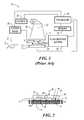
- a system 10 employed to form the relief patternincludes a stage 11 upon which a substrate 12 is supported, and a template 14 having a mold 16 with a patterning surface 18 thereon. Patterning surface 18 may be substantially smooth and/or planar, or may be patterned so that one or more recesses are formed therein.
- Template 14is coupled to an imprint head 20 to facilitate movement of template 14 .
- a fluid dispense system 22is coupled to be selectively placed in fluid communication with substrate 12 so as to deposit polymerizable material 24 thereon.
- a source 26 of energy 28is coupled to direct energy 28 along a path 30 .
- Imprint head 20 and stage 11are configured to arrange mold 16 and substrate 12 , respectively, to be in superimposition, and disposed in path 30 . Either imprint head 20 , stage 11 , or both vary a distance between mold 16 and substrate 12 to define a desired volume therebetween that is filled by polymerizable material 24 .
- polymerizable material 24is disposed upon substrate 12 before the desired volume is defined between mold 16 and substrate 12 .
- polymerizable material 24may fill the volume after the desired volume has been obtained.
- source 26produces energy 28 , which causes polymerizable material 24 to solidify and/or cross-link, forming polymeric material conforming to the shape of the substrate surface 25 and mold surface 18 .
- Control of this processis regulated by processor 32 that is in data communication with stage 11 imprint head 20 , fluid dispense system 22 , and source 26 , operating on a computer-readable program stored in memory 34 .
- One criterion associated with accurately transforming a pattern into a polymerizable materialis to reduce, if not prevent, adhesion to the template of the solidified layer, while ensuring suitable adhesion to the substrate. This is referred to as preferential release and adhesion properties. By preferential release and adhesion, the pattern recorded in the solidified layer is not distorted during separation of the template.
- a method to improve the adhesion of the solidified layer to the substrateis to introduce an adhesion primer layer (or primer layer).
- the adhesion primer layerneeds to adhere well to both the solidified layer and the substrate.
- the adhesion primer layeris put down by a spin coating method. After one side is coated, the wafer is flipped and the coated side physically touches part of spin coating apparatus in order to coat the second side. The physical contact between the spin coating apparatus and the coated surface can result in particle contamination of the adhesion primer layer.
- utilizing the spin coating process to apply the adhesion primer layermay limit the overall throughput of the process.
- the inventionfeatures a method including the steps of: (a) contacting a fluid with a surface of a substrate in a coating process, wherein a component of the fluid has a first functional group on a first end of the component and a second functional group on a second end of the component; (b) initiating a first chemical reaction that forms a first covalent bond between the first end of the component and the surface of the substrate such that an adhesion primer layer is adhered to the surface of the substrate; and (c) adhering a polymeric layer to the surface of the substrate with an imprint lithography process.
- the adheringincludes: (i) depositing a polymerizable material on the adhesion primer layer on the surface of the substrate, (ii) initiating polymerization of the polymerizable material to form a polymeric layer, and (iii) initiating a second chemical reaction between the second functional group of the component in the adhesion primer layer and the polymerizable material to adhere the polymeric layer to the surface of the substrate.
- Implementations of the inventioncan include one or more of the following features. Some embodiments include substantially simultaneously contacting the fluid with the surface of the substrate and with a second surface of the substrate in the coating process, and substantially simultaneously adhering the adhesion primer layer to the surface of the substrate and a second adhesion primer layer to the second surface of the substrate.
- Some embodimentsmay further include adhering a second polymeric layer to the second surface of the substrate with an imprint lithography process, wherein the adhering comprises: (a) depositing a second polymerizable material on the second adhesion primer layer on the second surface of the substrate, (b) initiating polymerization of the second polymerizable material to form a second polymeric layer, and (c) initiating the second chemical reaction between the second functional group of the component in the second adhesion primer layer and the second polymerizable material to adhere the second polymeric layer to the second surface of the substrate.
- the surface of the substrate and the second surface of the substratemay be substantially parallel.
- the componentmay include a first functional group at the first end of the component.
- the first functional groupmay be a leaving group.
- the fluidis a vapor
- the coating processis a chemical vapor deposition process.
- the vapormay be formed from a liquid.
- the fluidis a liquid
- the coating processis a dip-coating process.
- the fluidmay include an additional component, and the method may include copolymerizing the component with the additional component.
- initiating the first chemical reactionincludes heating.
- Initiating the second chemical reactionmay include exposing the polymerizable material to UV radiation.
- the substrateincludes silicon.
- the substratemay be chosen from a group consisting of silicon, silicon oxide silicon nitride, tantalum, aluminum, quartz, and fused silica.
- the substratemay include magnetic media.
- the inventionfeatures a method including contacting a substrate with a multi-functional component, covalently bonding the tetravalent atom of the first end of the multi-functional component to the substrate to form an adhesion primer layer; and covalently bonding the second end of the multi-functional component to a polymerizable material during an imprint lithography process.
- the multi-functional componentincludes a first end, a second end, and a linker group between the first end and the second end.
- the first endincludes a tetravalent atom
- the linker groupis a hydrocarbon group with up to three carbon atoms.
- the multi-functional componentmay have a boiling point that is at most about 350° C. and/or a viscosity that is at most about 100 cP.
- the linker groupmay be —CH 2 —.
- the tetravalent atommay be silicon.
- the multi-functional componentmay be acryloxymethyltrimethoxysilane, Acryloxymethyltriethoxysilane, acryloxypropyltrichlorosilane, and/or acryloxypropyl-trimethoxysilane.
- the substratemay be contacted with one or more additional components.
- An additional componentmay be 1,2-bis(trimethoxy-silyl)ethane and/or 1,6-bis(trichlorosilyl)hexane.
- the substratemay include silicon.
- the substrateis chosen from a group consisting of silicon, silicon oxide silicon nitride, tantalum, aluminum, quartz, and fused silica.
- features from specific embodimentsmay be combined with features from other embodiments.
- features from one embodimentmay be combined with features from any of the other embodiments.
- additional featuresmay be added to the specific embodiments described herein.
- FIG. 1is a simplified plan view of a lithographic system in accordance with the prior art
- FIG. 2is a simplified elevation view of a template and imprinting material disposed on a substrate in accordance with the present invention
- FIG. 3is a simplified elevation view of the template and substrate, shown in FIG. 2 , with the imprinting material being shown as patterned and solidified upon the layer;
- FIG. 4is a cross-sectional view of the template contacting imprinting material demonstrating the formation of the weak boundary lamella between solidified imprinting material and a template;
- FIG. 5is a detailed view of the droplets of imprint material, shown in FIG. 2 , showing the bifurcation of the droplets into surfactant-rich regions and surfactant-depleted regions;
- FIG. 6is a detailed view of a layer of imprinting material, deposited employing spin-on techniques, showing the bifurcation of the layer into surfactant-rich regions and surfactant-depleted regions;
- FIG. 7is a cross-sectional view of the template contacting solidified imprinting material, deposited as shown in either FIG. 5 or 6 , formed on a substrate including a primer layer;
- FIG. 8is a plan view showing the chemical structure of a component that may be used to form an adhesion primer layer
- FIG. 9is a plan view showing the chemical structure of another component that may be used to form an adhesion primer layer
- FIG. 10is a plan view showing the chemical structure of another component that may be used to form an adhesion primer layer
- FIG. 11is a plan view showing the chemical structure of another component that may be used to form an adhesion primer layer.
- FIG. 12is a plan view showing the chemical structure of another component that may be used to form an adhesion primer layer.
- a mold 36in accordance with the present invention, may be employed in system 10 , and may define a surface having a substantially smooth or planar profile (not shown).
- mold 36may include features defined by a plurality of spaced-apart recessions 38 and protrusions 40 .
- the plurality of featuresdefines an original pattern that forms the basis of a pattern to be formed on a substrate 42 .
- Substrate 42may comprise a bare wafer or a wafer with one or more layers disposed thereon, one of which is shown as primer layer 45 . To that end, reduced is a distance “d” between mold 36 and substrate 42 .
- the features on mold 36may be imprinted into a conformable region of substrate 42 , such as an imprinting or polymerizable material disposed on a portion of surface 44 that presents a substantially planar profile.
- the imprinting materialmay be deposited using any known technique, e.g., spin-coating, dip coating and the like. In the present example, however, the imprinting material is deposited as a plurality of spaced-apart discrete droplets 46 on substrate 42 . Imprinting material is formed from a composition that may be selectively polymerized and cross-linked to record the original pattern therein, defining a recorded pattern.
- the pattern recorded in the imprinting materialis produced, in part, by interaction with mold 36 , e.g., electrical interaction, magnetic interaction, thermal interaction, mechanical interaction or the like.
- mold 36comes into mechanical contact with the imprinting material, spreading droplets 36 , so as to generate a contiguous formation 50 of the imprinting material (a polymeric layer) over surface 44 .
- distance “d”is reduced to allow sub-portions 52 of imprinting material to ingress into and fill recessions 38 .
- the atmosphere between mold 36 and droplets 46is saturated with helium or is completely evacuated or is a partially evacuated atmosphere of helium.
- the imprinting materialis provided with the requisite properties to completely fill recessions 38 while covering surface 44 with a contiguous formation of the imprinting material.
- sub-portions 54 of imprinting material in superimposition with protrusions 40remain after the desired, usually minimum, distance “d” has been reached.
- This actionprovides formation 50 with sub-portions 52 having a thickness t 1 , and sub-portions 54 , having a thickness t 2 .
- Thicknesses “t 1 ” and “t 2 ”may be any thickness desired, dependent upon the application.
- formation 50is solidified by exposing the same to the appropriate curing agent, e.g., energy, such as electromagnetic radiation, thermal energy or the like, depending upon the imprinting material.
- formation 50is solidified to provide side 56 thereof with a shape conforming to a shape of a surface 58 of mold 36 .
- the characteristics of the imprinting materialare important to efficiently pattern substrate 42 in light of the unique patterning process employed.
- the imprinting materialit is desired that the imprinting material have certain characteristics to facilitate rapid and even filling of the features of mold 36 so that all thicknesses t 1 are substantially uniform and all thicknesses t 2 are substantially uniform.
- the viscosity of the imprinting materialit is desirable that the viscosity of the imprinting material be established, based upon the deposition process employed, to achieve the aforementioned characteristics.
- the imprinting materialmay be deposited on substrate 42 employing various techniques.
- a composition from which the imprinting material is formedhave relatively low viscosity, e.g., in a range of 0.5 to 20 centipoise (cP).
- cPcentipoise
- the compositionprovides the imprinting material with certain solidified phase characteristics.
- substrate 42may be formed from silicon, plastics, gallium arsenide, mercury telluride, and composites thereof.
- substrate 42may include one or more layers shown as primer layer 45 , e.g., dielectric layer, metal layer, semiconductor layer, planarization layer and the like, upon which formation 50 is generated.
- primer layer 45would be deposited upon a wafer 47 employing any suitable technique, such as chemical vapor deposition, spin-coating and the like.
- primer layer 45may be formed from any suitable material, such as silicon, germanium and the like.
- mold 36may be formed from several materials, e.g., fused-silica, quartz, indium tin oxide diamond-like carbon, MoSi, sol-gels and the like.
- composition from which formation 50 is generatedmay be fabricated from several different families of bulk materials.
- the compositionmay be fabricated from vinyl ethers, methacrylates, epoxies, thiolenes and acrylates, etc.
- An exemplary bulk material from which to form formation 50is as follows:
- the acrylate componentisobornyl acrylate (IBOA)
- IBOAisobornyl acrylate
- IBOAis Sartomer Company, Inc. of Exton, Pa. available under the product name SR 506.
- n-hexyl acrylate(n-HA) has the following structure:
- n-HAis employed to reduce the viscosity of the prior art bulk material so that bulk material, in the liquid phase, has a viscosity in a range 2-9 Centipoises, inclusive.
- An exemplary source for the n-HA componentis the Aldrich Chemical Company of Milwaukee, Wis.
- a cross-linking componentethylene glycol diacrylate, has the following structure:
- EGDAalso contributes to the modulus and stiffness buildup, as well as facilitates cross-linking of n-HA and IBOA during polymerization of the bulk material.
- An initiator component2-hydroxy-2-methyl-1-phenyl-propan-1-one is available from Ciba Specialty Chemicals of Tarrytown, N.Y. under the trade name DAROCUR® 1173, and has the following structure:
- the electromagnetic radiation to which the initiator is responsiveis broad band ultra-violet energy generated by a medium-pressure mercury lamp. In this manner, the initiator facilitates cross-linking and polymerization of the components of the bulk material.
- composition for the imprinting materialthat includes one of several compositions, such as the BULK IMPRINTING MATERIAL discussed above, along with a component that contains low surface energy groups, referred to as a surfactant component and fully described in U.S. Patent Application Publication No. 20060111454.
- the surfactant componentrises, after a period of time, to the air liquid interface, providing droplets 146 of imprinting material with a bifurcated concentration of materials.
- droplets 146include a higher concentration of the surfactant component, referred to as a surfactant-component-rich (SCR) sub-portion 136 , than the second portion, referred to as a surfactant-component-depleted (SCD) sub-portion 137 .
- SCR sub-rich sub-portion 136a surfactant-component-rich
- SCD sub-portion 137is positioned between surface 44 and SCR sub-portion 136 .
- SCR sub-portion 136attenuates the adhesion forces between mold 36 and the imprinting material, once the imprinting material is solidified.
- the surfactant componenthas opposed ends.
- the imprinting materialis in the liquid phase, i.e., polymerizable, one of the opposed ends has an affinity for the bulk material included in the imprinting material.
- the remaining endhas a fluorine component.
- the surfactant componentis orientated so that the fluorine component extends from an air-liquid interface defined by the imprinting material and the surrounding ambient.
- Lamella 60Upon solidification of the imprinting material, a first portion of the imprinting material generates a lamella 60 and a second portion of the imprinting material is solidified, i.e., polymeric material shown as formation 50 .
- Lamella 60is positioned between formation 50 and mold 36 .
- Lamella 60results from the presence and location of the fluorine components in the SCR sub-portion 136 .
- Lamella 60prevents strong adhesion forces from being developed between mold 36 and formation 50 .
- formation 50has first and second opposed sides 62 and 64 .
- Side 62adheres to mold 36 with a first adhesion force.
- Side 64adheres to substrate 42 with a second adhesion force.
- Lamella 60results in the first adhesion force being less than the second adhesion force.
- mold 36may be easily removed from formation 50 while minimizing distortions and/or the force required to separate mold 36 therefrom.
- formation 50is shown with side 62 being patterned, it should be understood that side
- lamella 60so as to be disposed between formation 50 and substrate 42 .
- Thismay be achieved, for example, by applying imprinting material to mold 36 and subsequently contacting substrate 42 with the imprinting material on mold 36 .
- formation 50will be disposed between lamella 60 and the body, e.g., mold 36 or substrate 42 , upon which the polymerizable material is deposited.
- the imprinting material depositedemploying spin-coating techniques, similar bifurcated concentration of materials occurs, as shown in FIG. 6 with respect to SCR sub-portion 236 and second and SCD sub-portion 237 .
- the time required for the bifurcationis dependent upon several factors, including the size of molecules in the composition and the viscosity of the composition. Only a few seconds is needed to achieve the aforementioned bifurcation of composition with viscosity below 20 cP. Material with viscosity in the hundreds of cP, however, may require a few seconds to several minutes.
- lamella 60may not be uniform. Some regions of lamella 60 are thinner than others, and in some extreme cases, lamella 60 may be absent in an extremely small percentage of the template surface so that template 36 is in contact with formation 50 . As a result of the thinner regions of lamella 60 and in the absence of lamella 60 , distortion and/or delamination of formation 50 from substrate 42 may occur. Specifically, upon separation of mold 36 , formation 50 is subjected to a separation force F S . Separation force F S is attributable to a pulling force F P on mold 36 and adhering forces, e.g., Van der Waals forces, between formation 50 and mold 36 as reduced by lamella 60 .
- separation force F Sis attributable to a pulling force F P on mold 36 and adhering forces, e.g., Van der Waals forces, between formation 50 and mold 36 as reduced by lamella 60 .
- lamella 60 separation force F Stypically has a magnitude that is less than the magnitude of an adhering force F A between formation 50 and substrate 42 .
- local separation force F Smay approach the magnitude of local adhering force F A .
- local forceswhat is meant are the forces present in a given region of lamella layer 60 , which in this example are the local forces proximate to a thin region of lamella layer 60 or where lamella layer 60 is substantially absent. This leads to distortion and/or delamination of formation 50 from substrate 42 .
- a more complex situationexists due to the presence of two interfaces 66 and 68 .
- a first adhering force F 1is present between primer layer 45 and formation 50 .
- a second adhering force, F 2is present between primer layer 45 and wafer 47 .
- the separation force F Shave a magnitude that is less than either adhering forces F 1 and F 2 .
- separation force F Smay be similar or approach the magnitude of one or both of adhering forces F 1 and F 2 . This may cause delamination of formation 50 from primer layer 45 , primer layer 45 from wafer 47 or both.
- primer layer 45is formed from a composition that forms strong bonds at interface 66 , i.e., between primer layer 45 and formation 50 , as well as, i.e., between interface 66 , primer layer 45 and wafer 47 .
- the compositionmay include one or more components.
- the compositionincludes one component and moisture (H 2 O) from the atmosphere that may be used, for instance, in a hydrolysis reaction.
- adhesion between primer layer 45 and formation 50 at first interface 66is the result of covalent bonding, i.e., covalent bonds between the composition from which primer layer 45 is formed and the composition from which formation 50 is formed are present.
- Adhesion between primer layer 45 and wafer 47may be achieved through any one of various mechanisms. These mechanisms may include covalent bonds formed between the composition from which primer layer 45 is formed and the material from which wafer 47 is formed. Alternatively, or in addition to, the covalent bonds, ionic bonds may be formed between the composition from which primer layer 45 is formed and the material from which wafer 47 is formed. Alternatively, or in addition to, the covalent bonds, and/or the ionic bonds or both, adhesion between the composition from which primer layer 45 is formed and the material from which wafer 47 is formed may be achieved vis-à-vis Van der Waals forces.
- adhesion primer layer 45from a composition that includes one or more components generally represented as follows:
- Compositions for the adhesion primer layermay include components I, II, or III or combinations thereof.
- Components I, II, and IIIinclude a first end, a second end, and a linker group (R, R′, R′′).
- R, R′, R′′a linker group
- the first endmay be thought of as including YX n Z 3-n
- the first end of component IIImay be thought of as including W.
- the second endmay be thought of as including X′.
- X′is a functional group that may bond covalently with the imprinting monomer (polymerizable material) during activation such as, for instance, UV irradiation.
- the imprinting monomerpolymerizable material
- X′may be, for instance, an acrylic group or a methacrylic group.
- Yis a tetravalent atom including, but not limited to, Si
- Xis a functional group (for instance, a leaving group) which allows the Y—X bond to be hydrolyzed to Y—OH. The hydroxyl group may subsequently react with the imprinting substrate to form a covalent bond with the substrate.
- Xmay be, for instance —OCH 3 , —OCH 2 CH 3 , —Cl, —OC( ⁇ O)CH 3 , etc.
- n and mrange from 1 to 3, inclusive.
- a higher number of leaving groupsmay allow for multiple bonding to a substrate (for instance, a surface of a substrate) and/or to other molecules in the adhesion primer layer, increasing the strength of adhesion of the adhesion primer layer to the surface of the substrate.
- Zis generally an unreactive group which fulfills the tetravalent requirement of Y.
- Zmay be, for instance, a methyl group.
- Wis an acidic functional group that may react or interact with imprinting substrate.
- Wis, for instance, carboxylic acid or phosphoric acid, etc.
- R, R′, and R′′are linker groups with different lengths.
- Typical linkersare hydrocarbon based.
- the linker groupsmay include, for instance, 1-10 or more carbons atoms (alkyl groups, ethylenically unsaturated groups, aromatic groups).
- a linker groupmay be chosen for a variety of factors including, but not limited to length, rigidity, and/or bond strength(s) of the linker group
- Xis selected to achieve cross-reaction of an end of component I and II (for instance, the first end) with the material from which substrate 42 is formed to adhere thereto by forming a covalent bond therewith, ionic bond therewith, and/or Van der Waals forces with the surface of the substrate. This may be achieved directly or indirectly. That is, if X is a leaving group, X does not directly react with the surface of the substrate. In this embodiment, a chemical reaction involving the leaving of X allows Y to chemically react to form a covalent bond with the surface of the substrate.
- functional groups Xmay participate in the cross-linking and polymerization reactions of adhesion primer layer 45 .
- X functional groupsmay facilitate polymerization and cross-linking in response to an activation energy that differs from the activation energy in response to which X′ functional groups cross-react.
- the X functional groupsmay facilitate cross-linking of molecules in primer layer 45 in response to exposure to thermal energy.
- Functional groups Xare selected to facilitate cross-reaction with substrate 42 through mechanisms including but not limited to: 1) direct reaction with material from which substrate 42 is formed; 2) reaction with cross-linker molecules with a linking functional group of the cross-linker reacting with substrate 42 ; 3) polymerization of and cross-linking of primer layer 45 so that chains of molecules of sufficient length may be developed to connect between formation 50 (polymeric layer) and surface of substrate 42 ; and 4) leaving of X to allow Y to achieve 1-3 above, which allows the polymeric layer to adhere to the surface of the substrate.
- X′is selected to achieve cross-reaction with the polymerizable material from which formation 50 (polymeric layer) is formed to form a covalent bond therebetween.
- the functionality of the X′ groupis established so the cross-reaction occurs during polymerization of formation 50 .
- the selection of functional group X′depends upon the characteristics of the polymerizable material from which formation 50 (polymeric layer) is formed.
- X′is chosen to react with the functional groups of the composition from which formation 50 is formed.
- X′may include acrylic, vinyl ether, and or methacrylic groups, and/or functional groups that may copolymerize with acrylic groups in formation 50 .
- X′ functional groupscross-react in response to activation such as, for instance, ultraviolet radiation.
- an exemplary multi-functional reactive compound Athat may be employed to form primer layer 45 in the presence of formation 50 being formed from BULK MATERIAL includes acryloxymethyltrimethoxysilane (Gelest, Inc., Morristown, Pa.). Acryloxymethyltrimethoxysilane has the following structure:
- the X′ functional group 70provides acrylic functionality for bonding with imprinting material.
- Functional groups 70 and 72are coupled to opposing ends of a backbone component or linker group 74 .
- Acryloxymethyltrimethoxysilanewith a flash point of about 60° C., has a boiling point of about 170° C., or about 20° C. lower than the boiling point of tridecafluoro-1,1,2,2-tetrahydrooctyltrichlorosilane (FOTS) self-assembling monolayer (SAM), which is known in the art to be vapor depositable. It may be desirable to keep the boiling temperature low while meeting all the adhesion requirements, thus facilitating the vapor deposition process.
- FOTStridecafluoro-1,1,2,2-tetrahydrooctyltrichlorosilane
- SAMself-assembling monolayer
- backbone component 74includes one carbon atom.
- a short backbone componentmay hold the X′ and X functional groups together more securely, requiring more energy to break the X′ and X functional groups apart during mold separation. Therefore, a shorter backbone component may provide a stronger adhesion primer layer and may therefore a stronger bond between the polymerized material and the substrate than a longer backbone component.
- acryloxymethyltriethoxysilanemay be used as multi-functional reactive compound I.
- another multi-functional reactive compound Ithat may be employed to form primer layer 45 in the presence of formation 50 being formed from BULK MATERIAL includes acryloxypropyltrichlorosilane (Gelest, Inc.) that has the following structure:
- the X′ functional group 76provides acrylic functionality for bonding with imprinting material.
- Functional groups 76 and 78are coupled to opposing ends of a backbone component 80 .
- Backbone component 80includes three carbon atoms.
- another multi-functional reactive compound Ithat may be employed to form primer layer 45 in the presence of formation 50 being formed from BULK MATERIAL includes acryloxypropyltrimethoxysilane (Aldrich; Milwaukee, Wis.) that has the following structure:
- the X′ functional group 82provides acrylic functionality for bonding with imprinting material.
- Backbone component 86includes three carbon atoms.
- a multi-functional reactive compound IIthat may be employed to form primer layer 45 in the presence of formation 50 being formed from BULK MATERIAL includes 1,2-bis(trimethoxysilyl)ethane (Aldrich) that has the following structure:
- Backbone component 94includes two carbon atoms.
- a multi-functional reactive compound IIthat may be employed to form primer layer 45 in the presence of formation 50 being formed from BULK MATERIAL includes 1,6-bis(trichlorosilyl)hexane (Aldrich) that has the following structure:
- Backbone component 98includes six carbon atoms.
- IIImay be, for example, acrylic acid (Aldrich), with the following structure:
- components I, II, and/or III in the fluid stateare contacted with a substrate during a coating process to adhere an adhesion primer layer on the substrate.
- the coating processmay include any dip-coating or chemical vapor deposition process known in the art.
- An adhesion primer layermay include, for instance, I but not II and III; III but not I and II; I and II but not III; I and III but not II; or I, II, and III.
- the X functionality in IIallows II to serve as a chain extender for co-polymerization of I and II.
- a component of an adhesion primer layeris contacted with a surface of a substrate. Initiation of a chemical reaction between the primer layer composition and the substrate can allow a first end of component I and/or component II and/or the W functional group of component III to bond (for instance, covalently, ionically, or through Van der Waals forces) to the substrate.
- the a primer layer componentsinclude acryloxymethyltrimethoxysilane or acryloxypropyltrimethoxysilane
- the componentsbond to each other (as well as the substrate), to form a networked polymer coating on the surface of the substrate.
- co-polymerization of I and IImay enhance the networked polymer coating.
- Initiation of the chemical reactionmay be achieved, for instance, through heating of the primer layer composition and/or substrate.
- a method of initiating the chemical reaction between the primer layer composition and the substratedoes not affect the X′ functionality of components of the primer layer composition.
- heating of the primer layer compositionmay cause bonding of a first end of components I, II, or III to a surface of a substrate, directly or indirectly through functional groups, without causing a reaction of a second end of components I or III (that is, without altering the X′ functionality).
- the X′ functionalityreacts during a step in an imprint lithography process.
- the X′ functionalitymay react during UV exposure or irradiation of the imprinting material, such that the X′ functionality of components of the primer layer composition reacts to form covalent bonds with the monomer in the polymerizable imprinting material during polymerization to facilitate strong adhesion between the polymeric layer (formed from the polymerizable material) and the substrate.
- Vapor deposition of an adhesion primer layermay be achieved through any chemical vapor deposition method known in the art. For instance, vapor deposition may be achieved in a vacuum oven or with a track type tool compatible with a semiconductor manufacturing process.
- an adhesion primer layer compositionmay be vaporized by heating during a vapor deposition process.
- an adhesion primer layer compositionmay be vaporized by a combination of heating and reduced pressure during a vapor deposition process.
- an adhesion primer layer compositionmay be vaporized by bubbling the composition with a carrier gas such as nitrogen or argon.
- a boiling point of an adhesion primer layer composition at ambient pressuremay be, for instance, less than about 350° C. In some embodiments, a boiling temperature of an adhesion primer layer composition may be less than about 250° C.
- a deposition temperaturemay be lower than the boiling point of the adhesion primer layer composition in a reduced pressure environment or with a gas bubbling technique.
- an adhesion primer layermay be adhered to one surface of a substrate by chemical vapor deposition. In other embodiments, an adhesion primer layer may be adhered simultaneously to two or more surfaces of a substrate through chemical vapor deposition.
- a substratemay be positioned on, for instance, a pin lift to allow vapor to contact two or more surfaces of a substrate substantially simultaneously without turning or repositioning the substrate between coating of a first surface and a second surface of the substrate.
- vapor deposition of an adhesion primer layermay allow batch processing of substrates, thereby reducing the processing time required for wafer-to-wafer spin-coating processes conventionally used to deposit adhesion primer layers.
- vapor deposition of an adhesion primer layermay allow two or more surfaces of substrate to be coated with an adhesion primer layer without particle contamination caused during physical contact of a substrate and spin-coating apparatus, for instance, a spin chuck, during a spin-coating process.
- Adhesion primer layersmay be vapor deposited on two surfaces of a substrate that are substantially parallel.
- vapor deposition of an adhesion primer layerwill facilitate manufacturing of double-sided media, including magnetic media. Examples of double-sided media may include, for instance, compact discs, digital video discs, and hard discs.
- Components of an adhesion primer layer compositionmay be chosen for factors including, but not limited to, functionality (multi-functional or mono-functional), linker group length, linker rigidity, link bond strength(s), pH, cross-linking density, reactivity, shelf life and/or stability, and boiling temperature.
- the strength of the adhesion layermay be limited by properties of the linker group (for instance, the weakest bond in the linker group).
- a componentmay be chosen to have a short linker with a strong bond between X and X′ functionalities.
- a strong linker bondfor instance, some aromatic groups
- COMPOSITION 1is a 0.1% solution of acryloxymethyltrimethoxysilane (shown in FIG. 8 ) in isopropanol. This composition was applied by dip coating.
- COMPOSITION 2is a 0.1% solution of acryloxypropyltrimethoxysilane (APTMS) (shown in FIG. 10 ), in isopropanol. This composition was applied by dip coating.
- APITMSacryloxypropyltrimethoxysilane
- COMPOSITION 3is DUV30J-16, a bottom anti-reflective coating (BARC) (Brewer Science, Rolla, Mo.).
- DUV30J-16contains phenolic resins, and its cross-linker can react with carboxylic functional groups. It is believed that DUV30J-16 will not form covalent bonds with formation 50 .
- COMPOSITION 4includes approximately 77 grams of IsoRad 501 (available from Schenectady International, Inc. in Schenectady, N.Y.), 22 grams of Cymel 303ULF (Cytec Industries, Inc.; West Patterson, N.J.) and one gram of Cycat 4040 (Cytec Industries, Inc.). IsoRad 501, Cymel 303ULF and Cycat are combined. The combination of IsoRad 501, Cymel 303ULF and Cycat is then introduced into approximately 1900 grams of PM Acetate.
- PM Acetateis a product name of a solvent consisting of 2-(1-methoxy)propyl acetate (Eastman Chemical Company; Kingsport, Tenn.).
- Glass slidesapproximately 1 mm thick, 75 ⁇ 25 mm in the lateral dimension, were dip-coated with COMPOSITIONS 1-2 to generate comparative data of the strength of the adhesion forces of interfaces 66 and 68 .
- COMPOSITIONS 1-2are deposited onto glass slides employing dip-coating techniques known in the art.
- COMPOSITIONS 3-4are deposited onto glass slides employing spin-coating techniques known in the art.
- primer layer 45is dried on the glass slides on hot plates at 80° C. for 10 minutes.
- primer layer 45is dried on the glass slides on hot plates at 180° C. for 2 minutes.
- primer layer 45is dried on the glass slides on hot plates at 150° C. for 5 minutes.
- dip- and spin-coated COMPOSITIONS 1-4are solidified, i.e., polymerized and cross-linked, by exposure to thermal energy.
- a drop of BULK IMPRINTING MATERIALis applied to a center of a coated side of a first glass slide.
- the BULK IMPRINTING MATERIALis then sandwiched between two primer layers 45 by having the primer layer on the two glass slides facing one another and contacting BULK IMPRINTING MATERIAL.
- a longitudinal axis of one of the two glass slidesextends orthogonally to the longitudinal axis of the remaining glass slide to form a “t” shape, with an overlapping area of about 25 ⁇ 25 mm.
- the BULK IMPRINTING MATERIALis solidified, i.e., polymerized, and cross-linked by exposing the two glass slides to actinic energy, such as broad band ultraviolet wavelengths, using a medium pressure mercury UV lamp for 40 seconds at 20 mW/cm 2 intensity.
- COMPOSITIONS 2 and 3demonstrated similar adhesion values of about 4 lbf. Under the same testing, COMPOSITIONS 1 and 4 resulted in broken slide(s) before the true adhesion was measured. Adhesion at the time of breaking (minimum adhesion) was measured to be about 12 lbf. Thus, COMPOSITIONS 1 and 4 demonstrated adhesion of at least about 3 times stronger than the adhesion of COMPOSITIONS 2 and 3 under similar conditions.
- acryloxymethyltrimethoxysilane(from COMPOSITION 1) was vapor deposited by bubbler and heating methods. Adhesion properties of vapor-deposited acryloxymethyltrimethoxysilane were compared to adhesion properties of spin-coated COMPOSITION 4. This demonstration utilized 65 mm glass discs as supplied by Hitachi Global Storage Technologies (San Jose, Calif.) with 5 nm of surface Si x N y coating. Substrates were taken straight from the carrier without precleaning.
- a 65 mm substratewas set on an aluminum slide, the aluminum slide is partially covered by this substrate, and the aluminum slide was positioned on a hot plate.
- the hot platewas maintained at 90° C. 3 ⁇ L of acryloxymethyltrimethoxysilane was dispensed on the uncovered portion of the aluminum slide.
- a lidwas placed over both the substrate and aluminum slide to retain the vapor generated by heat. The retained vapor was deposited onto the substrates. Substrates were removed after 1 minute, and exposed to ambient conditions for 20 minutes before conducting the adhesion test. Glass rods with a 5 mm diameter were also coated with acryloxymethyltrimethoxysilane in a similar manner.
- COMPOSITION 3was spin-coated on substrates and exposed to ambient conditions for 20 minutes before conducting the adhesion test. Glass rods with a 5 mm diameter were brush-coated with COMPOSITION 3.
- COMPOSITION 4was spin-coated on substrates and exposed to ambient conditions for 20 minutes before conducting the adhesion test. Glass rods with a 5 mm diameter were brush-coated with COMPOSITION 4.
- the adhesion testwas conducted by placing a drop of BULK IMPRINTING MATERIAL on the coated substrate, and positioning a coated glass rod on the substrate, such that the glass rod was substantially perpendicular to the lateral plane of the substrate.
- the imprinting materialwas cured with ultraviolet radiation. With the glass rod anchored on the substrate, shear testing of the glass rod was performed to assess adhesion of the glass rod to the substrate. That is, the adhesion force was recorded as the force required to shear the glass rod from the substrate.
- Shear testingresulted in shear force of about 35 lbf for COMPOSITION 1 (about 37 lbf for the evaporation method and about 33 lbf for the bubbler method), and and 10 lbf for spin-coated COMPOSITION 3.
- the shear force of COMPOSITION 1is about 3.5 times the shear force of COMPOSITION 3
- the true adhesion in the form of the peel of COMPOSITION 1is more than 3.5 times of that of COMPOSITION 3 once the friction forces is removed from the shear force.
Landscapes
- Engineering & Computer Science (AREA)
- Chemical & Material Sciences (AREA)
- Nanotechnology (AREA)
- Physics & Mathematics (AREA)
- Crystallography & Structural Chemistry (AREA)
- General Physics & Mathematics (AREA)
- Mathematical Physics (AREA)
- Organic Chemistry (AREA)
- Condensed Matter Physics & Semiconductors (AREA)
- Manufacturing & Machinery (AREA)
- Polymers & Plastics (AREA)
- Theoretical Computer Science (AREA)
- Health & Medical Sciences (AREA)
- Chemical Kinetics & Catalysis (AREA)
- Medicinal Chemistry (AREA)
- Life Sciences & Earth Sciences (AREA)
- Wood Science & Technology (AREA)
- Shaping Of Tube Ends By Bending Or Straightening (AREA)
- Exposure Of Semiconductors, Excluding Electron Or Ion Beam Exposure (AREA)
- Laminated Bodies (AREA)
- Manufacturing Of Magnetic Record Carriers (AREA)
- Application Of Or Painting With Fluid Materials (AREA)
Abstract
Description
- isobornyl acrylate
- n-hexyl acrylate
- ethylene glycol diacrylate
- 2-hydroxy-2-methyl-1-phenyl-propan-1-one

and comprises approximately 47% of bulk material by weight, but may be present in a range of 20% to 80%, inclusive. As a result, the mechanical properties of

and comprises approximately 25% of bulk material by weight, but may be present in a range of 0% to 50%, inclusive. Also providing flexibility to

and comprises approximately 25% of bulk material by weight, and may be present in a range of 10% to 50%, inclusive. EGDA also contributes to the modulus and stiffness buildup, as well as facilitates cross-linking of n-HA and IBOA during polymerization of the bulk material.

and comprises approximately 3% of the bulk material by weight, and may be present in a range of 1% to 5%, inclusive. The electromagnetic radiation to which the initiator is responsive is broad band ultra-violet energy generated by a medium-pressure mercury lamp. In this manner, the initiator facilitates cross-linking and polymerization of the components of the bulk material.

Compositions for the adhesion primer layer may include components I, II, or III or combinations thereof. Components I, II, and III include a first end, a second end, and a linker group (R, R′, R″). For instance, in components I and II, the first end may be thought of as including YXnZ3-n, while the first end of component III may be thought of as including W. Similarly, in Components I and III, the second end may be thought of as including X′.

The X′

The X′

The X′

The X functional groups88 (m=3) and90 (n=3) include three methoxy leaving groups bound to Y (tetravalent Si).

The X functional groups94 (m=3) and96 (n=3) include three —Cl leaving groups bound to Y (tetravalent Si).

Claims (20)
Priority Applications (9)
| Application Number | Priority Date | Filing Date | Title |
|---|---|---|---|
| US11/734,542US8808808B2 (en) | 2005-07-22 | 2007-04-12 | Method for imprint lithography utilizing an adhesion primer layer |
| KR1020097021203AKR101536217B1 (en) | 2007-04-12 | 2008-03-19 | Method for imprint lithography utilizing an adhesion primer layer |
| MYPI20094023AMY153677A (en) | 2007-04-12 | 2008-03-19 | Method for imprint lithography utilizing an adhesion primer layer |
| PCT/US2008/057518WO2008127835A1 (en) | 2007-04-12 | 2008-03-19 | Method for imprint lithography utilizing an adhesion primer layer |
| JP2010503115AJP5399374B2 (en) | 2007-04-12 | 2008-03-19 | Method for imprint lithography utilizing an adhesive primer layer |
| CN2008800115510ACN101702886B (en) | 2007-04-12 | 2008-03-19 | Imprint lithography method using adhesion primer layer |
| EP08744071AEP2136933A4 (en) | 2007-04-12 | 2008-03-19 | Method for imprint lithography utilizing an adhesion primer layer |
| TW97110543ATWI432892B (en) | 2007-04-12 | 2008-03-25 | Method for imprint lithography utilizing an adhesion primer layer |
| US12/326,709US8846195B2 (en) | 2005-07-22 | 2008-12-02 | Ultra-thin polymeric adhesion layer |
Applications Claiming Priority (3)
| Application Number | Priority Date | Filing Date | Title |
|---|---|---|---|
| US11/187,407US8557351B2 (en) | 2005-07-22 | 2005-07-22 | Method for adhering materials together |
| US11/187,406US7759407B2 (en) | 2005-07-22 | 2005-07-22 | Composition for adhering materials together |
| US11/734,542US8808808B2 (en) | 2005-07-22 | 2007-04-12 | Method for imprint lithography utilizing an adhesion primer layer |
Related Parent Applications (2)
| Application Number | Title | Priority Date | Filing Date |
|---|---|---|---|
| US11/187,406Continuation-In-PartUS7759407B2 (en) | 2005-07-22 | 2005-07-22 | Composition for adhering materials together |
| US11/187,407Continuation-In-PartUS8557351B2 (en) | 2005-07-22 | 2005-07-22 | Method for adhering materials together |
Related Child Applications (1)
| Application Number | Title | Priority Date | Filing Date |
|---|---|---|---|
| US11/187,407Continuation-In-PartUS8557351B2 (en) | 2005-07-22 | 2005-07-22 | Method for adhering materials together |
Publications (2)
| Publication Number | Publication Date |
|---|---|
| US20070212494A1 US20070212494A1 (en) | 2007-09-13 |
| US8808808B2true US8808808B2 (en) | 2014-08-19 |
Family
ID=39864653
Family Applications (1)
| Application Number | Title | Priority Date | Filing Date |
|---|---|---|---|
| US11/734,542Active2027-04-25US8808808B2 (en) | 2005-07-22 | 2007-04-12 | Method for imprint lithography utilizing an adhesion primer layer |
Country Status (8)
| Country | Link |
|---|---|
| US (1) | US8808808B2 (en) |
| EP (1) | EP2136933A4 (en) |
| JP (1) | JP5399374B2 (en) |
| KR (1) | KR101536217B1 (en) |
| CN (1) | CN101702886B (en) |
| MY (1) | MY153677A (en) |
| TW (1) | TWI432892B (en) |
| WO (1) | WO2008127835A1 (en) |
Cited By (14)
| Publication number | Priority date | Publication date | Assignee | Title |
|---|---|---|---|---|
| EP3141956A1 (en) | 2015-09-08 | 2017-03-15 | Canon Kabushiki Kaisha | Substrate pretreatment for reducing fill time in nanoimprint lithography |
| US9773672B2 (en) | 2015-02-09 | 2017-09-26 | Samsung Electronics Co., Ltd. | Method of forming micropatterns |
| US9811671B1 (en) | 2000-05-24 | 2017-11-07 | Copilot Ventures Fund Iii Llc | Authentication method and system |
| US9846814B1 (en) | 2008-04-23 | 2017-12-19 | Copilot Ventures Fund Iii Llc | Authentication method and system |
| US10095106B2 (en) | 2016-03-31 | 2018-10-09 | Canon Kabushiki Kaisha | Removing substrate pretreatment compositions in nanoimprint lithography |
| US10134588B2 (en) | 2016-03-31 | 2018-11-20 | Canon Kabushiki Kaisha | Imprint resist and substrate pretreatment for reducing fill time in nanoimprint lithography |
| US10317793B2 (en) | 2017-03-03 | 2019-06-11 | Canon Kabushiki Kaisha | Substrate pretreatment compositions for nanoimprint lithography |
| US10488753B2 (en) | 2015-09-08 | 2019-11-26 | Canon Kabushiki Kaisha | Substrate pretreatment and etch uniformity in nanoimprint lithography |
| US10509313B2 (en) | 2016-06-28 | 2019-12-17 | Canon Kabushiki Kaisha | Imprint resist with fluorinated photoinitiator and substrate pretreatment for reducing fill time in nanoimprint lithography |
| US10620539B2 (en) | 2016-03-31 | 2020-04-14 | Canon Kabushiki Kaisha | Curing substrate pretreatment compositions in nanoimprint lithography |
| US10754244B2 (en) | 2016-03-31 | 2020-08-25 | Canon Kabushiki Kaisha | Pattern forming method as well as production methods for processed substrate, optical component, circuit board, electronic component and imprint mold |
| US10829644B2 (en) | 2016-03-31 | 2020-11-10 | Canon Kabushiki Kaisha | Pattern forming method as well as production methods for processed substrate, optical component, circuit board, electronic component and imprint mold |
| US10883006B2 (en) | 2016-03-31 | 2021-01-05 | Canon Kabushiki Kaisha | Pattern forming method as well as production methods for processed substrate, optical component, circuit board, electronic component and imprint mold |
| US11520226B2 (en) | 2017-05-12 | 2022-12-06 | Canon Kabushiki Kaisha | Imprint method, imprint apparatus, imprint system, and method of manufacturing article |
Families Citing this family (36)
| Publication number | Priority date | Publication date | Assignee | Title |
|---|---|---|---|---|
| US8294025B2 (en) | 2002-06-08 | 2012-10-23 | Solarity, Llc | Lateral collection photovoltaics |
| US7307118B2 (en)* | 2004-11-24 | 2007-12-11 | Molecular Imprints, Inc. | Composition to reduce adhesion between a conformable region and a mold |
| US7906180B2 (en)* | 2004-02-27 | 2011-03-15 | Molecular Imprints, Inc. | Composition for an etching mask comprising a silicon-containing material |
| US7759407B2 (en) | 2005-07-22 | 2010-07-20 | Molecular Imprints, Inc. | Composition for adhering materials together |
| US8808808B2 (en) | 2005-07-22 | 2014-08-19 | Molecular Imprints, Inc. | Method for imprint lithography utilizing an adhesion primer layer |
| US8846195B2 (en) | 2005-07-22 | 2014-09-30 | Canon Nanotechnologies, Inc. | Ultra-thin polymeric adhesion layer |
| US8557351B2 (en)* | 2005-07-22 | 2013-10-15 | Molecular Imprints, Inc. | Method for adhering materials together |
| US8142703B2 (en)* | 2005-10-05 | 2012-03-27 | Molecular Imprints, Inc. | Imprint lithography method |
| US9323143B2 (en)* | 2008-02-05 | 2016-04-26 | Canon Nanotechnologies, Inc. | Controlling template surface composition in nano-imprint lithography |
| US8415010B2 (en)* | 2008-10-20 | 2013-04-09 | Molecular Imprints, Inc. | Nano-imprint lithography stack with enhanced adhesion between silicon-containing and non-silicon containing layers |
| US8361546B2 (en)* | 2008-10-30 | 2013-01-29 | Molecular Imprints, Inc. | Facilitating adhesion between substrate and patterned layer |
| US8529778B2 (en)* | 2008-11-13 | 2013-09-10 | Molecular Imprints, Inc. | Large area patterning of nano-sized shapes |
| US20110030770A1 (en) | 2009-08-04 | 2011-02-10 | Molecular Imprints, Inc. | Nanostructured organic solar cells |
| JP5583374B2 (en)* | 2009-09-07 | 2014-09-03 | 株式会社島津製作所 | Photo-curing resin characteristic testing device, holder used in the testing device, and characteristic testing method |
| WO2011066450A2 (en) | 2009-11-24 | 2011-06-03 | Molecular Imprints, Inc. | Adhesion layers in nanoimprint lithography |
| KR20130105648A (en)* | 2010-09-08 | 2013-09-25 | 몰레큘러 임프린츠 인코퍼레이티드 | Vapor delivery system for use in imprint lithography |
| JP5218521B2 (en)* | 2010-10-21 | 2013-06-26 | 大日本印刷株式会社 | Imprint method and transfer substrate and adhesive used therefor |
| KR102046933B1 (en) | 2010-11-05 | 2019-11-20 | 캐논 나노테크놀로지즈 인코퍼레이티드 | Patterning of non-convex shaped nanostructures |
| JP2012183753A (en)* | 2011-03-07 | 2012-09-27 | Fujifilm Corp | Nanoimprinting method |
| US20140242744A1 (en)* | 2011-09-26 | 2014-08-28 | Solarity, Inc. | Substrate and superstrate design and process for nano-imprinting lithography of light and carrier collection management devices |
| JP5767615B2 (en)* | 2011-10-07 | 2015-08-19 | 富士フイルム株式会社 | Underlayer film composition for imprint and pattern forming method using the same |
| WO2013051735A1 (en)* | 2011-10-07 | 2013-04-11 | Fujifilm Corporation | Underlay film composition for imprints and method of forming pattern and pattern formation method using the same |
| US9147423B2 (en)* | 2012-04-17 | 2015-09-29 | HGST Netherlands B.V. | Method for improving a patterned perpendicular magnetic recording disk with annealing |
| JP5899145B2 (en)* | 2012-06-18 | 2016-04-06 | 富士フイルム株式会社 | Composition for forming underlayer film for imprint and pattern forming method |
| JP2015210834A (en)* | 2014-04-25 | 2015-11-24 | 株式会社東芝 | Pattern formation method and manufacturing method of magnetic recording medium |
| EP3158578B1 (en)* | 2014-07-08 | 2024-01-10 | Canon Kabushiki Kaisha | Adhesion layer composition, method for forming film by nanoimprinting, methods for manufacturing optical component, circuit board and electronic apparatus |
| US10156786B2 (en) | 2015-09-30 | 2018-12-18 | Thomas E. Seidel | Method and structure for nanoimprint lithography masks using optical film coatings |
| KR101720895B1 (en) | 2016-01-20 | 2017-03-29 | 경희대학교 산학협력단 | Nanoimprinting method |
| KR102607657B1 (en) | 2016-06-07 | 2023-11-28 | 티씨엘 차이나 스타 옵토일렉트로닉스 테크놀로지 컴퍼니 리미티드 | Method for forming fine pattern |
| JP7112220B2 (en)* | 2017-05-12 | 2022-08-03 | キヤノン株式会社 | Methods, apparatus, systems, and methods of manufacturing articles |
| US11634529B2 (en)* | 2017-06-16 | 2023-04-25 | Fujifilm Electronic Materials U.S.A., Inc. | Multilayer structure |
| JP7017623B2 (en)* | 2018-03-07 | 2022-02-08 | 富士フイルム株式会社 | Underlayer film forming composition for imprint, curable composition for imprint, kit |
| TWI771575B (en)* | 2018-03-27 | 2022-07-21 | 日商富士軟片股份有限公司 | Underlayer film forming composition for imprinting, set, curable composition for imprinting, laminate, method for producing laminate, method for forming pattern, and method for producing semiconductor device |
| US10780682B2 (en) | 2018-12-20 | 2020-09-22 | Canon Kabushiki Kaisha | Liquid adhesion composition, multi-layer structure and method of making said structure |
| EP3929658A1 (en) | 2020-06-23 | 2021-12-29 | Koninklijke Philips N.V. | Imprinting method and patterned layer |
| US12325046B2 (en)* | 2022-06-28 | 2025-06-10 | Canon Kabushiki Kaisha | Superstrate including a body and layers and methods of forming and using the same |
Citations (244)
| Publication number | Priority date | Publication date | Assignee | Title |
|---|---|---|---|---|
| US3498827A (en)* | 1966-02-02 | 1970-03-03 | Exxon Research Engineering Co | Abrasion resistant metal articles |
| US3810874A (en) | 1969-03-10 | 1974-05-14 | Minnesota Mining & Mfg | Polymers prepared from poly(perfluoro-alkylene oxide) compounds |
| US4251277A (en) | 1978-04-24 | 1981-02-17 | Sws Silicones Corporation | Compositions containing thiofunctional polysiloxanes |
| US4506003A (en) | 1980-06-21 | 1985-03-19 | Hoechst Aktiengesellschaft | Positive-working radiation-sensitive mixture |
| US4512848A (en) | 1984-02-06 | 1985-04-23 | Exxon Research And Engineering Co. | Procedure for fabrication of microstructures over large areas using physical replication |
| US4614667A (en) | 1984-05-21 | 1986-09-30 | Minnesota Mining And Manufacturing Company | Composite low surface energy liner of perfluoropolyether |
| US4617238A (en) | 1982-04-01 | 1986-10-14 | General Electric Company | Vinyloxy-functional organopolysiloxane compositions |
| US4687707A (en) | 1984-06-26 | 1987-08-18 | Asahi Glass Company Ltd. | Low reflectance transparent material having antisoiling properties |
| US4731155A (en) | 1987-04-15 | 1988-03-15 | General Electric Company | Process for forming a lithographic mask |
| US4826943A (en) | 1986-07-25 | 1989-05-02 | Oki Electric Industry Co., Ltd. | Negative resist material |
| US4848911A (en) | 1986-06-11 | 1989-07-18 | Kabushiki Kaisha Toshiba | Method for aligning first and second objects, relative to each other, and apparatus for practicing this method |
| US4931351A (en) | 1987-01-12 | 1990-06-05 | Eastman Kodak Company | Bilayer lithographic process |
| US4959252A (en) | 1986-09-29 | 1990-09-25 | Rhone-Poulenc Chimie | Highly oriented thermotropic optical disc member |
| US5028511A (en) | 1989-05-30 | 1991-07-02 | E. I. Du Pont De Nemours And Company | Process for preparing a precolored image using photosensitive reproduction element containing a photorelease layer |
| US5028366A (en) | 1988-01-12 | 1991-07-02 | Air Products And Chemicals, Inc. | Water based mold release compositions for making molded polyurethane foam |
| US5110514A (en) | 1989-05-01 | 1992-05-05 | Soane Technologies, Inc. | Controlled casting of a shrinkable material |
| US5148037A (en) | 1988-09-09 | 1992-09-15 | Canon Kabushiki Kaisha | Position detecting method and apparatus |
| US5149592A (en) | 1990-05-09 | 1992-09-22 | Avery Dennison Corporation | Ultraviolet radiation curable clearcoat |
| US5151754A (en) | 1989-10-06 | 1992-09-29 | Kabushiki Kaisha Toshiba | Method and an apparatus for measuring a displacement between two objects and a method and an apparatus for measuring a gap distance between two objects |
| US5169494A (en) | 1989-03-27 | 1992-12-08 | Matsushita Electric Industrial Co., Ltd. | Fine pattern forming method |
| US5206983A (en) | 1991-06-24 | 1993-05-04 | Wisconsin Alumni Research Foundation | Method of manufacturing micromechanical devices |
| US5240550A (en) | 1990-09-21 | 1993-08-31 | U.S. Philips Corp. | Method of forming at least one groove in a substrate layer |
| US5242711A (en) | 1991-08-16 | 1993-09-07 | Rockwell International Corp. | Nucleation control of diamond films by microlithographic patterning |
| US5259926A (en) | 1991-09-24 | 1993-11-09 | Hitachi, Ltd. | Method of manufacturing a thin-film pattern on a substrate |
| US5298556A (en) | 1992-07-21 | 1994-03-29 | Tse Industries, Inc. | Mold release composition and method coating a mold core |
| EP0592972A2 (en)* | 1992-10-13 | 1994-04-20 | INSTITUT FÜR MIKROTECHNIK MAINZ GmbH | Resist coated metal- or semiconductor-substrate having a stable resist-substrate adhesion |
| US5314731A (en) | 1991-05-17 | 1994-05-24 | Asahi Glass Company Ltd. | Surface-treated substrate |
| US5318870A (en) | 1989-10-18 | 1994-06-07 | Massachusetts Institute Of Technology | Method of patterning a phenolic polymer film without photoactive additive through exposure to high energy radiation below 225 nm with subsequent organometallic treatment and the associated imaged article |
| US5331020A (en) | 1991-11-14 | 1994-07-19 | Dow Corning Limited | Organosilicon compounds and compositions containing them |
| US5362940A (en) | 1990-11-09 | 1994-11-08 | Litel Instruments | Use of Fresnel zone plates for material processing |
| US5369722A (en) | 1991-09-18 | 1994-11-29 | Schott Glaswerke | Optical inorganic waveguide with a substantially planar organic substrate |
| US5368942A (en) | 1993-01-15 | 1994-11-29 | The United States Of America As Represented By The Secreatary Of Commerce | Method of adhering substrates |
| US5371822A (en) | 1992-06-09 | 1994-12-06 | Digital Equipment Corporation | Method of packaging and assembling opto-electronic integrated circuits |
| US5374454A (en) | 1990-09-18 | 1994-12-20 | International Business Machines Incorporated | Method for conditioning halogenated polymeric materials and structures fabricated therewith |
| US5380474A (en) | 1993-05-20 | 1995-01-10 | Sandia Corporation | Methods for patterned deposition on a substrate |
| US5389696A (en) | 1993-09-17 | 1995-02-14 | Miles Inc. | Process for the production of molded products using internal mold release agents |
| US5395954A (en) | 1992-07-20 | 1995-03-07 | Societe Des Ceramiques Techniques | Organic-inorganic polycondensate and a method of obtaining the same |
| US5425848A (en) | 1993-03-16 | 1995-06-20 | U.S. Philips Corporation | Method of providing a patterned relief of cured photoresist on a flat substrate surface and device for carrying out such a method |
| US5432700A (en) | 1992-12-21 | 1995-07-11 | Ford Motor Company | Adaptive active vehicle suspension system |
| US5439766A (en) | 1988-12-30 | 1995-08-08 | International Business Machines Corporation | Composition for photo imaging |
| US5458953A (en) | 1991-09-12 | 1995-10-17 | Mannington Mills, Inc. | Resilient floor covering and method of making same |
| US5459198A (en) | 1994-07-29 | 1995-10-17 | E. I. Du Pont De Nemours And Company | Fluoroinfused composites, articles of manufacture formed therefrom, and processes for the preparation thereof |
| US5462700A (en) | 1993-11-08 | 1995-10-31 | Alliedsignal Inc. | Process for making an array of tapered photopolymerized waveguides |
| US5480047A (en) | 1993-06-04 | 1996-01-02 | Sharp Kabushiki Kaisha | Method for forming a fine resist pattern |
| US5482768A (en) | 1993-05-14 | 1996-01-09 | Asahi Glass Company Ltd. | Surface-treated substrate and process for its production |
| WO1996000656A1 (en) | 1994-06-30 | 1996-01-11 | Elf Atochem S.A. | Packaging material including a silica layer and a polyolefin layer |
| US5512131A (en) | 1993-10-04 | 1996-04-30 | President And Fellows Of Harvard College | Formation of microstamped patterns on surfaces and derivative articles |
| US5527662A (en) | 1990-05-24 | 1996-06-18 | Matsushita Electric Industrial Co., Ltd. | Process for forming fine pattern |
| US5542978A (en) | 1994-06-10 | 1996-08-06 | Johnson & Johnson Vision Products, Inc. | Apparatus for applying a surfactant to mold surfaces |
| US5545367A (en)* | 1992-04-15 | 1996-08-13 | Soane Technologies, Inc. | Rapid prototype three dimensional stereolithography |
| US5550196A (en) | 1994-11-09 | 1996-08-27 | Shell Oil Company | Low viscosity adhesive compositions containing asymmetric radial polymers |
| US5578683A (en) | 1994-06-27 | 1996-11-26 | Avery Dennison Corporation | Crosslinkable graft pressure-sensitive adhesives |
| US5594042A (en) | 1993-05-18 | 1997-01-14 | Dow Corning Corporation | Radiation curable compositions containing vinyl ether functional polyorganosiloxanes |
| US5601641A (en) | 1992-07-21 | 1997-02-11 | Tse Industries, Inc. | Mold release composition with polybutadiene and method of coating a mold core |
| US5629095A (en) | 1993-05-18 | 1997-05-13 | Dow Corning Corporation | Radiation curable compositions containing vinyl ether functional polysiloxanes and methods for the preparation |
| US5629128A (en) | 1994-10-31 | 1997-05-13 | Fuji Photo Film Co., Ltd. | Positive photoresist composition |
| US5669303A (en) | 1996-03-04 | 1997-09-23 | Motorola | Apparatus and method for stamping a surface |
| US5723242A (en) | 1996-03-28 | 1998-03-03 | Minnesota Mining And Manufacturing Company | Perfluoroether release coatings for organic photoreceptors |
| US5725788A (en) | 1996-03-04 | 1998-03-10 | Motorola | Apparatus and method for patterning a surface |
| US5772905A (en) | 1995-11-15 | 1998-06-30 | Regents Of The University Of Minnesota | Nanoimprint lithography |
| US5776748A (en) | 1993-10-04 | 1998-07-07 | President And Fellows Of Harvard College | Method of formation of microstamped patterns on plates for adhesion of cells and other biological materials, devices and uses therefor |
| US5812629A (en) | 1997-04-30 | 1998-09-22 | Clauser; John F. | Ultrahigh resolution interferometric x-ray imaging |
| US5820769A (en) | 1995-05-24 | 1998-10-13 | Regents Of The University Of Minnesota | Method for making magnetic storage having discrete elements with quantized magnetic moments |
| US5837314A (en) | 1994-06-10 | 1998-11-17 | Johnson & Johnson Vision Products, Inc. | Method and apparatus for applying a surfactant to mold surfaces |
| US5849222A (en) | 1995-09-29 | 1998-12-15 | Johnson & Johnson Vision Products, Inc. | Method for reducing lens hole defects in production of contact lens blanks |
| US5849209A (en) | 1995-03-31 | 1998-12-15 | Johnson & Johnson Vision Products, Inc. | Mold material made with additives |
| US5858580A (en) | 1997-09-17 | 1999-01-12 | Numerical Technologies, Inc. | Phase shifting circuit manufacture method and apparatus |
| US5888650A (en) | 1996-06-03 | 1999-03-30 | Minnesota Mining And Manufacturing Company | Temperature-responsive adhesive article |
| US5895263A (en) | 1996-12-19 | 1999-04-20 | International Business Machines Corporation | Process for manufacture of integrated circuit device |
| US5942302A (en) | 1996-02-23 | 1999-08-24 | Imation Corp. | Polymer layer for optical media |
| US5948470A (en) | 1997-04-28 | 1999-09-07 | Harrison; Christopher | Method of nanoscale patterning and products made thereby |
| US5974150A (en) | 1997-09-30 | 1999-10-26 | Tracer Detection Technology Corp. | System and method for authentication of goods |
| EP0592139B1 (en) | 1992-10-06 | 1999-10-27 | Ciba SC Holding AG | Composition for priming and cleaning based on organosilane |
| US6015609A (en) | 1996-04-04 | 2000-01-18 | Navartis Ag | Process for manufacture of a porous polymer from a mixture |
| US6046056A (en) | 1996-06-28 | 2000-04-04 | Caliper Technologies Corporation | High throughput screening assay systems in microscale fluidic devices |
| US6060530A (en) | 1996-04-04 | 2000-05-09 | Novartis Ag | Process for manufacture of a porous polymer by use of a porogen |
| US6063888A (en) | 1996-04-09 | 2000-05-16 | Dsm N.V. | Liquid curable resin composition |
| US6074827A (en) | 1996-07-30 | 2000-06-13 | Aclara Biosciences, Inc. | Microfluidic method for nucleic acid purification and processing |
| US6117708A (en) | 1998-02-05 | 2000-09-12 | Micron Technology, Inc. | Use of residual organic compounds to facilitate gate break on a carrier substrate for a semiconductor device |
| US6132632A (en) | 1997-09-11 | 2000-10-17 | International Business Machines Corporation | Method and apparatus for achieving etch rate uniformity in a reactive ion etcher |
| US6146811A (en) | 1998-08-01 | 2000-11-14 | Korea Advanced Institute Of Science And Technology | Photoresist using dioxaspiro ring-substituted acryl derivatives |
| US6160030A (en) | 1996-04-04 | 2000-12-12 | Novartis Ag | High water content porous polymer |
| US6174931B1 (en) | 1991-02-28 | 2001-01-16 | 3M Innovative Properties Company | Multi-stage irradiation process for production of acrylic based compositions and compositions made thereby |
| US6174932B1 (en) | 1998-05-20 | 2001-01-16 | Denovus Llc | Curable sealant composition |
| US6190929B1 (en) | 1999-07-23 | 2001-02-20 | Micron Technology, Inc. | Methods of forming semiconductor devices and methods of forming field emission displays |
| US6200736B1 (en) | 1998-04-15 | 2001-03-13 | Etec Systems, Inc. | Photoresist developer and method |
| US6204343B1 (en) | 1996-12-11 | 2001-03-20 | 3M Innovative Properties Company | Room temperature curable resin |
| US6218316B1 (en) | 1998-10-22 | 2001-04-17 | Micron Technology, Inc. | Planarization of non-planar surfaces in device fabrication |
| US6225367B1 (en) | 1998-09-15 | 2001-05-01 | Novartis Ag | Polymers |
| US6261469B1 (en) | 1998-10-13 | 2001-07-17 | Honeywell International Inc. | Three dimensionally periodic structural assemblies on nanometer and longer scales |
| US6274294B1 (en) | 1999-02-03 | 2001-08-14 | Electroformed Stents, Inc. | Cylindrical photolithography exposure process and apparatus |
| WO2001063605A1 (en) | 2000-02-22 | 2001-08-30 | Krauss-Maffei Kunststofftechnik Gmbh | Method and device for producing a dvd |
| US6309580B1 (en) | 1995-11-15 | 2001-10-30 | Regents Of The University Of Minnesota | Release surfaces, particularly for use in nanoimprint lithography |
| US20010044075A1 (en) | 2000-04-25 | 2001-11-22 | Jsr Corporation | Radiation sensitive resin composition for forming barrier ribs for an EL display element, barrier rib and EL display element |
| US6326627B1 (en) | 2000-08-02 | 2001-12-04 | Archimedes Technology Group, Inc. | Mass filtering sputtered ion source |
| US6334960B1 (en) | 1999-03-11 | 2002-01-01 | Board Of Regents, The University Of Texas System | Step and flash imprint lithography |
| US6344105B1 (en) | 1999-06-30 | 2002-02-05 | Lam Research Corporation | Techniques for improving etch rate uniformity |
| US6348999B1 (en) | 1995-05-10 | 2002-02-19 | Epigem Limited | Micro relief element and preparation thereof |
| JP2002060529A (en) | 2000-08-22 | 2002-02-26 | Fuji Photo Film Co Ltd | High-adhesion hard coated film |
| US6355198B1 (en) | 1996-03-15 | 2002-03-12 | President And Fellows Of Harvard College | Method of forming articles including waveguides via capillary micromolding and microtransfer molding |
| US20020042027A1 (en) | 1998-10-09 | 2002-04-11 | Chou Stephen Y. | Microscale patterning and articles formed thereby |
| US6391217B2 (en) | 1999-12-23 | 2002-05-21 | University Of Massachusetts | Methods and apparatus for forming submicron patterns on films |
| US6399406B2 (en) | 2000-06-19 | 2002-06-04 | International Business Machines Corporation | Encapsulated MEMS band-pass filter for integrated circuits and method of fabrication thereof |
| US20020072009A1 (en) | 2000-12-13 | 2002-06-13 | Kim Hyun-Woo | Photosensitive polymer containing Si, Ge or Sn and resist composition comprising the same |
| US20020094496A1 (en) | 2000-07-17 | 2002-07-18 | Choi Byung J. | Method and system of automatic fluid dispensing for imprint lithography processes |
| US20020123592A1 (en) | 2001-03-02 | 2002-09-05 | Zenastra Photonics Inc. | Organic-inorganic hybrids surface adhesion promoter |
| WO2002069040A1 (en) | 2001-02-27 | 2002-09-06 | Shipley Company, Llc | Novel polymers, processes for polymer synthesis and photoresist compositions |
| US6446933B1 (en) | 1998-09-03 | 2002-09-10 | Micron Technology, Inc. | Film on a surface of a mold used during semiconductor device fabrication |
| US6447919B1 (en) | 1997-02-03 | 2002-09-10 | Cytonix Corporation | Hydrophobic coating compositions, articles coated with said compositions, and processes for manufacturing same |
| US20020132482A1 (en) | 2000-07-18 | 2002-09-19 | Chou Stephen Y. | Fluid pressure imprint lithography |
| US20020135099A1 (en) | 2001-01-19 | 2002-09-26 | Robinson Timothy R. | Mold with metal oxide surface compatible with ionic release agents |
| US20020146642A1 (en) | 2001-04-04 | 2002-10-10 | Kim Hyun-Woo | Photosensitive polymers and resist compositions comprising the photosensitive polymers |
| US6468642B1 (en) | 1995-10-03 | 2002-10-22 | N.V. Bekaert S.A. | Fluorine-doped diamond-like coatings |
| US6475704B1 (en) | 1997-09-12 | 2002-11-05 | Canon Kabushiki Kaisha | Method for forming fine structure |
| US20020168578A1 (en) | 1996-09-18 | 2002-11-14 | Numerical Technologies, Inc. | Phase shifting circuit manufacture method and apparatus |
| US20020170880A1 (en) | 2001-03-22 | 2002-11-21 | Yong Chen | Scanning probe based lithographic alignment |
| JP2002355543A (en) | 2001-01-25 | 2002-12-10 | Sekisui Chem Co Ltd | Dispersant, heat developable photosensitive material, ceramic green sheet, primer for plastic lens, recording agent for water base ink and adhesive for metallic foil |
| US6495624B1 (en) | 1997-02-03 | 2002-12-17 | Cytonix Corporation | Hydrophobic coating compositions, articles coated with said compositions, and processes for manufacturing same |
| US6498640B1 (en) | 1999-12-30 | 2002-12-24 | Koninklijke Philips Electronics N.V. | Method to measure alignment using latent image grating structures |
| US6497961B2 (en) | 1999-02-22 | 2002-12-24 | 3M Innovative Properties Company | Ceramer composition and composite comprising free radically curable fluorochemical component |
| US6503914B1 (en) | 2000-10-23 | 2003-01-07 | Board Of Regents, The University Of Texas System | Thienopyrimidine-based inhibitors of the Src family |
| US20030017368A1 (en) | 1999-05-07 | 2003-01-23 | Junhua Wu | Elastomeric lubricants for magnetic recording media |
| US20030025895A1 (en) | 2001-08-03 | 2003-02-06 | Michael Binnard | Apparatus and methods for detecting tool-induced shift in microlithography apparatus |
| US6518168B1 (en) | 1995-08-18 | 2003-02-11 | President And Fellows Of Harvard College | Self-assembled monolayer directed patterning of surfaces |
| US6518189B1 (en) | 1995-11-15 | 2003-02-11 | Regents Of The University Of Minnesota | Method and apparatus for high density nanostructures |
| US6517977B2 (en) | 2001-03-28 | 2003-02-11 | Motorola, Inc. | Lithographic template and method of formation and use |
| US6517995B1 (en) | 1999-09-14 | 2003-02-11 | Massachusetts Institute Of Technology | Fabrication of finely featured devices by liquid embossing |
| US20030054115A1 (en) | 2001-09-14 | 2003-03-20 | Ralph Albano | Ultraviolet curing process for porous low-K materials |
| US6541356B2 (en) | 2001-05-21 | 2003-04-01 | International Business Machines Corporation | Ultimate SIMOX |
| US20030062334A1 (en) | 2001-09-25 | 2003-04-03 | Lee Hong Hie | Method for forming a micro-pattern on a substrate by using capillary force |
| US6544594B2 (en) | 1999-09-10 | 2003-04-08 | Nano-Tex, Llc | Water-repellent and soil-resistant finish for textiles |
| US20030080472A1 (en) | 2001-10-29 | 2003-05-01 | Chou Stephen Y. | Lithographic method with bonded release layer for molding small patterns |
| US20030081193A1 (en) | 2001-06-01 | 2003-05-01 | White Donald L. | Holder, system, and process for improving overlay in lithography |
| US6565776B1 (en) | 1999-06-11 | 2003-05-20 | Bausch & Lomb Incorporated | Lens molds with protective coatings for production of contact lenses and other ophthalmic products |
| US6580172B2 (en) | 2001-03-02 | 2003-06-17 | Motorola, Inc. | Lithographic template and method of formation and use |
| US20030137494A1 (en) | 2000-05-01 | 2003-07-24 | Tulbert David J. | Human-machine interface |
| US6605849B1 (en) | 2002-02-14 | 2003-08-12 | Symmetricom, Inc. | MEMS analog frequency divider |
| US6610458B2 (en) | 2001-07-23 | 2003-08-26 | Kodak Polychrome Graphics Llc | Method and system for direct-to-press imaging |
| US20030166814A1 (en) | 2002-02-28 | 2003-09-04 | David Sparrowe | Prepolymer material, polymer material, imprinting process and their use |
| WO2003073164A2 (en) | 2002-02-27 | 2003-09-04 | Brewer Science, Inc. | Novel planarization method for multi-layer lithography processing |
| EP1342736A2 (en) | 2002-02-28 | 2003-09-10 | MERCK PATENT GmbH | Prepolymer material, polymer material, imprinting process and their Use |
| US6621960B2 (en) | 2002-01-24 | 2003-09-16 | Oplink Communications, Inc. | Method of fabricating multiple superimposed fiber Bragg gratings |
| US20030174435A1 (en) | 2002-03-18 | 2003-09-18 | International Business Machines Corporation | Method and apparatus for providing an aligned coil for an inductive head structure using a patterned seed layer |
| US20030186140A1 (en) | 2001-06-27 | 2003-10-02 | Fries David P. | Maskless photolithography for using photoreactive agents |
| WO2003087935A2 (en) | 2002-04-17 | 2003-10-23 | Clariant Gmbh | Nanoimprint resist |
| US6646662B1 (en) | 1998-05-26 | 2003-11-11 | Seiko Epson Corporation | Patterning method, patterning apparatus, patterning template, and method for manufacturing the patterning template |
| US6649272B2 (en) | 2001-11-08 | 2003-11-18 | 3M Innovative Properties Company | Coating composition comprising fluorochemical polyether silane polycondensate and use thereof |
| US6664026B2 (en) | 2001-03-22 | 2003-12-16 | International Business Machines Corporation | Method of manufacturing high aspect ratio photolithographic features |
| US6664306B2 (en) | 2000-09-08 | 2003-12-16 | 3M Innovative Properties Company | Crosslinkable polymeric compositions and use thereof |
| US6667082B2 (en) | 1997-01-21 | 2003-12-23 | Cryovac, Inc. | Additive transfer film suitable for cook-in end use |
| US20030235787A1 (en) | 2002-06-24 | 2003-12-25 | Watts Michael P.C. | Low viscosity high resolution patterning material |
| JP2004051706A (en) | 2002-07-17 | 2004-02-19 | Fuji Photo Film Co Ltd | Hard coat-treated article and method for producing the same |
| US6696220B2 (en) | 2000-10-12 | 2004-02-24 | Board Of Regents, The University Of Texas System | Template for room temperature, low pressure micro-and nano-imprint lithography |
| US20040037956A1 (en) | 2002-08-22 | 2004-02-26 | Eastman Kodak Company | Method of coating micro-electromechanical devices |
| US20040036201A1 (en) | 2000-07-18 | 2004-02-26 | Princeton University | Methods and apparatus of field-induced pressure imprint lithography |
| WO2004021083A1 (en) | 2002-08-27 | 2004-03-11 | Obducat Ab | Device for transferring a pattern to an object |
| DE10237280A1 (en) | 2002-08-14 | 2004-03-11 | Micronas Holding Gmbh | Process for connecting surfaces, semiconductors with bonded surfaces as well as bio-chip and bio-sensor |
| US20040046288A1 (en) | 2000-07-18 | 2004-03-11 | Chou Stephen Y. | Laset assisted direct imprint lithography |
| US20040065252A1 (en) | 2002-10-04 | 2004-04-08 | Sreenivasan Sidlgata V. | Method of forming a layer on a substrate to facilitate fabrication of metrology standards |
| US20040065976A1 (en) | 2002-10-04 | 2004-04-08 | Sreenivasan Sidlgata V. | Method and a mold to arrange features on a substrate to replicate features having minimal dimensional variability |
| US6721529B2 (en) | 2001-09-21 | 2004-04-13 | Nexpress Solutions Llc | Release agent donor member having fluorocarbon thermoplastic random copolymer overcoat |
| US6720076B2 (en) | 2002-05-31 | 2004-04-13 | Omnova Solutions Inc. | In-mold primer coating for thermoplastic substrates |
| US6737489B2 (en) | 2001-05-21 | 2004-05-18 | 3M Innovative Properties Company | Polymers containing perfluorovinyl ethers and applications for such polymers |
| US20040110096A1 (en) | 2001-04-10 | 2004-06-10 | Takahiro Kishioka | Composition for forming antireflection film for lithography |
| US20040110856A1 (en) | 2002-12-04 | 2004-06-10 | Young Jung Gun | Polymer solution for nanoimprint lithography to reduce imprint temperature and pressure |
| US20040116548A1 (en) | 2002-12-12 | 2004-06-17 | Molecular Imprints, Inc. | Compositions for dark-field polymerization and method of using the same for imprint lithography processes |
| US20040127613A1 (en) | 2002-12-11 | 2004-07-01 | Shin-Etsu Chemical Co., Ltd. | Radiation curing silicone rubber composition, adhesive silicone elastomer film formed from same, semiconductor device using same, and method of producing semiconductor device |
| US20040131718A1 (en) | 2000-07-18 | 2004-07-08 | Princeton University | Lithographic apparatus for fluid pressure imprint lithography |
| US20040137734A1 (en) | 1995-11-15 | 2004-07-15 | Princeton University | Compositions and processes for nanoimprinting |
| US6774183B1 (en) | 2000-04-27 | 2004-08-10 | Bostik, Inc. | Copolyesters having improved retained adhesion |
| US20040156108A1 (en) | 2001-10-29 | 2004-08-12 | Chou Stephen Y. | Articles comprising nanoscale patterns with reduced edge roughness and methods of making same |
| US20040157078A1 (en) | 2001-01-25 | 2004-08-12 | Takahiro Yoshida | Polyvinyl acetal, polyvinyl acetal composition, ink coating material, dispersant, heat-developable photosensitive material,ceramic green sheet, primer for plastic lens, recording agent for water-based ink and adhesive for metal foil |
| US6776094B1 (en) | 1993-10-04 | 2004-08-17 | President & Fellows Of Harvard College | Kit For Microcontact Printing |
| US20040168613A1 (en) | 2003-02-27 | 2004-09-02 | Molecular Imprints, Inc. | Composition and method to form a release layer |
| US20040170770A1 (en) | 2003-02-27 | 2004-09-02 | Molecular Imprints, Inc. | Method to reduce adhesion between a polymerizable layer and a substrate employing a fluorine-containing layer |
| US20040175631A1 (en) | 2002-10-21 | 2004-09-09 | Nanoink, Inc. | Nanometer-scale engineered structures, methods and apparatus for fabrication thereof, and applications to mask repair, enhancement, and fabrications |
| US6790905B2 (en) | 2001-10-09 | 2004-09-14 | E. I. Du Pont De Nemours And Company | Highly repellent carpet protectants |
| US20040192041A1 (en) | 2003-03-27 | 2004-09-30 | Jun-Ho Jeong | UV nanoimprint lithography process using elementwise embossed stamp and selectively additive pressurization |
| US20040191429A1 (en) | 1999-08-17 | 2004-09-30 | Western Washington University | Liquid crystal imprinting |
| US20040188381A1 (en) | 2003-03-25 | 2004-09-30 | Molecular Imprints, Inc. | Positive tone bi-layer imprint lithography method |
| US20040197843A1 (en) | 2001-07-25 | 2004-10-07 | Chou Stephen Y. | Nanochannel arrays and their preparation and use for high throughput macromolecular analysis |
| US6802870B2 (en) | 2001-05-25 | 2004-10-12 | 3M Innovative Properties Company | Method for imparting soil and stain resistance to carpet |
| US20040202865A1 (en) | 2003-04-08 | 2004-10-14 | Andrew Homola | Release coating for stamper |
| US20040241338A1 (en) | 2001-11-07 | 2004-12-02 | Foster Kenneth L. | Planarized microelectronic substrates |
| US6830819B2 (en) | 2003-03-18 | 2004-12-14 | Xerox Corporation | Fluorosilicone release agent for fluoroelastomer fuser members |
| US20040250945A1 (en) | 2003-06-10 | 2004-12-16 | Industrial Technology Research Institute | Method for and apparatus for bonding patterned imprint to a substrate by adhering means |
| US20040259992A1 (en) | 2001-01-26 | 2004-12-23 | Roland Gobel | Adhesives for metal-polymer composites |
| EP1491356A2 (en) | 2003-06-25 | 2004-12-29 | Fuji Photo Film Co., Ltd. | Lithographic printing plate precursor and lithographic printing method |
| US6849558B2 (en) | 2002-05-22 | 2005-02-01 | The Board Of Trustees Of The Leland Stanford Junior University | Replication and transfer of microstructures and nanostructures |
| US20050037143A1 (en) | 2000-07-18 | 2005-02-17 | Chou Stephen Y. | Imprint lithography with improved monitoring and control and apparatus therefor |
| US6873087B1 (en) | 1999-10-29 | 2005-03-29 | Board Of Regents, The University Of Texas System | High precision orientation alignment and gap control stages for imprint lithography processes |
| US20050084804A1 (en) | 2003-10-16 | 2005-04-21 | Molecular Imprints, Inc. | Low surface energy templates |
| US20050098534A1 (en) | 2003-11-12 | 2005-05-12 | Molecular Imprints, Inc. | Formation of conductive templates employing indium tin oxide |
| US6900881B2 (en) | 2002-07-11 | 2005-05-31 | Molecular Imprints, Inc. | Step and repeat imprint lithography systems |
| US20050118749A1 (en) | 2002-02-19 | 2005-06-02 | Nissan Chemical Industries | Composition for forming anti-reflective coating |
| US6908861B2 (en) | 2002-07-11 | 2005-06-21 | Molecular Imprints, Inc. | Method for imprint lithography using an electric field |
| US6916584B2 (en) | 2002-08-01 | 2005-07-12 | Molecular Imprints, Inc. | Alignment methods for imprint lithography |
| US6916585B2 (en) | 2000-07-16 | 2005-07-12 | Board Of Regents, The University Of Texas Systems | Method of varying template dimensions to achieve alignment during imprint lithography |
| US20050156357A1 (en) | 2002-12-12 | 2005-07-21 | Board Of Regents, The University Of Texas System | Planarization method of patterning a substrate |
| US20050160934A1 (en) | 2004-01-23 | 2005-07-28 | Molecular Imprints, Inc. | Materials and methods for imprint lithography |
| US6932934B2 (en) | 2002-07-11 | 2005-08-23 | Molecular Imprints, Inc. | Formation of discontinuous films during an imprint lithography process |
| US20050187339A1 (en) | 2004-02-23 | 2005-08-25 | Molecular Imprints, Inc. | Materials for imprint lithography |
| US6936194B2 (en) | 2002-09-05 | 2005-08-30 | Molecular Imprints, Inc. | Functional patterning material for imprint lithography processes |
| US6957608B1 (en) | 2002-08-02 | 2005-10-25 | Kovio, Inc. | Contact print methods |
| US6958531B2 (en) | 2003-11-14 | 2005-10-25 | The Regents Of The University Of Michigan | Multi-substrate package and method for assembling same |
| US6964793B2 (en) | 2002-05-16 | 2005-11-15 | Board Of Regents, The University Of Texas System | Method for fabricating nanoscale patterns in light curable compositions using an electric field |
| US20060030071A1 (en) | 2004-08-05 | 2006-02-09 | Fujitsu Limited | Method for processing base |
| US20060029811A1 (en) | 2004-08-06 | 2006-02-09 | Nippon Shokubai Co., Ltd. | Resin composition, method of its composition, and cured formulation |
| US20060030653A1 (en) | 2004-08-04 | 2006-02-09 | Xerox Corporation | Polycarbonates and photoconductive imaging members |
| US20060035029A1 (en) | 2004-08-16 | 2006-02-16 | Molecular Imprints, Inc. | Method to provide a layer with uniform etch characteristics |
| US20060040058A1 (en)* | 2003-11-21 | 2006-02-23 | Babak Heidari | Multilayer nano imprint lithography |
| US20060046069A1 (en) | 2004-08-30 | 2006-03-02 | Jung Gun Y | Increasing adhesion in an imprinting procedure |
| US7011932B2 (en) | 2001-05-01 | 2006-03-14 | E. I. Du Pont De Nemours And Company | Polymer waveguide fabrication process |
| US20060062922A1 (en) | 2004-09-23 | 2006-03-23 | Molecular Imprints, Inc. | Polymerization technique to attenuate oxygen inhibition of solidification of liquids and composition therefor |
| US20060076717A1 (en) | 2002-07-11 | 2006-04-13 | Molecular Imprints, Inc. | Step and repeat imprint lithography processes |
| US20060081557A1 (en) | 2004-10-18 | 2006-04-20 | Molecular Imprints, Inc. | Low-k dielectric functional imprinting materials |
| US7037639B2 (en) | 2002-05-01 | 2006-05-02 | Molecular Imprints, Inc. | Methods of manufacturing a lithography template |
| US20060111454A1 (en) | 2004-11-24 | 2006-05-25 | Molecular Imprints, Inc. | Composition to reduce adhesion between a conformable region and a mold |
| US20060108710A1 (en) | 2004-11-24 | 2006-05-25 | Molecular Imprints, Inc. | Method to reduce adhesion between a conformable region and a mold |
| US20060145398A1 (en) | 2004-12-30 | 2006-07-06 | Board Of Regents, The University Of Texas System | Release layer comprising diamond-like carbon (DLC) or doped DLC with tunable composition for imprint lithography templates and contact masks |
| US20060188751A1 (en) | 2005-02-24 | 2006-08-24 | Tdk Corporation | Magnetic recording medium and magnetic recording/reproducing device |
| US20060222897A1 (en) | 2005-03-30 | 2006-10-05 | Kabushiki Kaisha Toshiba | Discrete track media and method of manufacturing the same |
| US7122482B2 (en) | 2003-10-27 | 2006-10-17 | Molecular Imprints, Inc. | Methods for fabricating patterned features utilizing imprint lithography |
| US7128875B2 (en) | 1995-04-10 | 2006-10-31 | Cubicciotti Roger S | Signal processing devices comprising biological and bio-mimetic components |
| US7138362B2 (en) | 2002-02-19 | 2006-11-21 | Kanto Kagaku Kabushiki Kaisha | Washing liquid composition for semiconductor substrate |
| US7141188B2 (en) | 2001-05-30 | 2006-11-28 | Honeywell International Inc. | Organic compositions |
| US20060279024A1 (en) | 2003-06-17 | 2006-12-14 | Molecular Imprints, Inc. | Method for providing desirable wetting and release characteristics between a mold and a polymerizable composition |
| US7163888B2 (en) | 2004-11-22 | 2007-01-16 | Motorola, Inc. | Direct imprinting of etch barriers using step and flash imprint lithography |
| US20070021520A1 (en)* | 2005-07-22 | 2007-01-25 | Molecular Imprints, Inc. | Composition for adhering materials together |
| US20070017631A1 (en) | 2005-07-22 | 2007-01-25 | Molecular Imprints, Inc. | Method for adhering materials together |
| US20070042173A1 (en) | 2005-08-22 | 2007-02-22 | Fuji Photo Film Co., Ltd. | Antireflection film, manufacturing method thereof, and polarizing plate using the same, and image display device |
| US20070051697A1 (en) | 2005-09-02 | 2007-03-08 | Dipietro Richard A | Processes and materials for step and flash imprint lithography |
| US20070059211A1 (en) | 2005-03-11 | 2007-03-15 | The College Of Wooster | TNT sensor containing molecularly imprinted sol gel-derived films |
| US20070212494A1 (en) | 2005-07-22 | 2007-09-13 | Molecular Imprints, Inc. | Method for Imprint Lithography Utilizing an Adhesion Primer Layer |
| US7309225B2 (en) | 2004-08-13 | 2007-12-18 | Molecular Imprints, Inc. | Moat system for an imprint lithography template |
| US20080110557A1 (en) | 2006-11-15 | 2008-05-15 | Molecular Imprints, Inc. | Methods and Compositions for Providing Preferential Adhesion and Release of Adjacent Surfaces |
| US20080131623A1 (en) | 2006-11-28 | 2008-06-05 | Wei Zhang | Method and apparatus to apply surface release coating for imprint mold |
| US7393789B2 (en) | 2005-09-01 | 2008-07-01 | Micron Technology, Inc. | Protective coating for planarization |
| US7396475B2 (en) | 2003-04-25 | 2008-07-08 | Molecular Imprints, Inc. | Method of forming stepped structures employing imprint lithography |
| US20090136654A1 (en) | 2005-10-05 | 2009-05-28 | Molecular Imprints, Inc. | Contact Angle Attenuations on Multiple Surfaces |
| US20090155583A1 (en) | 2005-07-22 | 2009-06-18 | Molecular Imprints, Inc. | Ultra-thin Polymeric Adhesion Layer |
| US20090197057A1 (en) | 2008-02-05 | 2009-08-06 | Molecular Imprints, Inc. | Controlling Template Surface Composition in Nano-Imprint Lithography |
| JP4330650B2 (en) | 2005-06-03 | 2009-09-16 | 中 奥村 | Medication support program |
| US20100112236A1 (en) | 2008-10-30 | 2010-05-06 | Molecular Imprints, Inc. | Facilitating Adhesion Between Substrate and Patterned Layer |
Family Cites Families (1)
| Publication number | Priority date | Publication date | Assignee | Title |
|---|---|---|---|---|
| JPH04330650A (en)* | 1991-05-01 | 1992-11-18 | Dainippon Ink & Chem Inc | Manufacturing method of optical disc substrate |
- 2007
- 2007-04-12USUS11/734,542patent/US8808808B2/enactiveActive
- 2008
- 2008-03-19KRKR1020097021203Apatent/KR101536217B1/enactiveActive
- 2008-03-19WOPCT/US2008/057518patent/WO2008127835A1/enactiveApplication Filing
- 2008-03-19MYMYPI20094023Apatent/MY153677A/enunknown
- 2008-03-19EPEP08744071Apatent/EP2136933A4/ennot_activeWithdrawn
- 2008-03-19CNCN2008800115510Apatent/CN101702886B/enactiveActive
- 2008-03-19JPJP2010503115Apatent/JP5399374B2/enactiveActive
- 2008-03-25TWTW97110543Apatent/TWI432892B/enactive
Patent Citations (281)
| Publication number | Priority date | Publication date | Assignee | Title |
|---|---|---|---|---|
| US3498827A (en)* | 1966-02-02 | 1970-03-03 | Exxon Research Engineering Co | Abrasion resistant metal articles |
| US3810874A (en) | 1969-03-10 | 1974-05-14 | Minnesota Mining & Mfg | Polymers prepared from poly(perfluoro-alkylene oxide) compounds |
| US4251277A (en) | 1978-04-24 | 1981-02-17 | Sws Silicones Corporation | Compositions containing thiofunctional polysiloxanes |
| US4506003A (en) | 1980-06-21 | 1985-03-19 | Hoechst Aktiengesellschaft | Positive-working radiation-sensitive mixture |
| US4617238A (en) | 1982-04-01 | 1986-10-14 | General Electric Company | Vinyloxy-functional organopolysiloxane compositions |
| US4512848A (en) | 1984-02-06 | 1985-04-23 | Exxon Research And Engineering Co. | Procedure for fabrication of microstructures over large areas using physical replication |
| US4614667A (en) | 1984-05-21 | 1986-09-30 | Minnesota Mining And Manufacturing Company | Composite low surface energy liner of perfluoropolyether |
| US4687707A (en) | 1984-06-26 | 1987-08-18 | Asahi Glass Company Ltd. | Low reflectance transparent material having antisoiling properties |
| US4848911A (en) | 1986-06-11 | 1989-07-18 | Kabushiki Kaisha Toshiba | Method for aligning first and second objects, relative to each other, and apparatus for practicing this method |
| US4826943A (en) | 1986-07-25 | 1989-05-02 | Oki Electric Industry Co., Ltd. | Negative resist material |
| US4959252A (en) | 1986-09-29 | 1990-09-25 | Rhone-Poulenc Chimie | Highly oriented thermotropic optical disc member |
| US4931351A (en) | 1987-01-12 | 1990-06-05 | Eastman Kodak Company | Bilayer lithographic process |
| US4731155A (en) | 1987-04-15 | 1988-03-15 | General Electric Company | Process for forming a lithographic mask |
| US5028366A (en) | 1988-01-12 | 1991-07-02 | Air Products And Chemicals, Inc. | Water based mold release compositions for making molded polyurethane foam |
| US5148037A (en) | 1988-09-09 | 1992-09-15 | Canon Kabushiki Kaisha | Position detecting method and apparatus |
| US5439766A (en) | 1988-12-30 | 1995-08-08 | International Business Machines Corporation | Composition for photo imaging |
| US5169494A (en) | 1989-03-27 | 1992-12-08 | Matsushita Electric Industrial Co., Ltd. | Fine pattern forming method |
| US5110514A (en) | 1989-05-01 | 1992-05-05 | Soane Technologies, Inc. | Controlled casting of a shrinkable material |
| US5028511A (en) | 1989-05-30 | 1991-07-02 | E. I. Du Pont De Nemours And Company | Process for preparing a precolored image using photosensitive reproduction element containing a photorelease layer |
| US5151754A (en) | 1989-10-06 | 1992-09-29 | Kabushiki Kaisha Toshiba | Method and an apparatus for measuring a displacement between two objects and a method and an apparatus for measuring a gap distance between two objects |
| US5318870A (en) | 1989-10-18 | 1994-06-07 | Massachusetts Institute Of Technology | Method of patterning a phenolic polymer film without photoactive additive through exposure to high energy radiation below 225 nm with subsequent organometallic treatment and the associated imaged article |
| US5149592A (en) | 1990-05-09 | 1992-09-22 | Avery Dennison Corporation | Ultraviolet radiation curable clearcoat |
| US5527662A (en) | 1990-05-24 | 1996-06-18 | Matsushita Electric Industrial Co., Ltd. | Process for forming fine pattern |
| US5374454A (en) | 1990-09-18 | 1994-12-20 | International Business Machines Incorporated | Method for conditioning halogenated polymeric materials and structures fabricated therewith |
| US5240550A (en) | 1990-09-21 | 1993-08-31 | U.S. Philips Corp. | Method of forming at least one groove in a substrate layer |
| US5362940A (en) | 1990-11-09 | 1994-11-08 | Litel Instruments | Use of Fresnel zone plates for material processing |
| US6174931B1 (en) | 1991-02-28 | 2001-01-16 | 3M Innovative Properties Company | Multi-stage irradiation process for production of acrylic based compositions and compositions made thereby |
| US5314731A (en) | 1991-05-17 | 1994-05-24 | Asahi Glass Company Ltd. | Surface-treated substrate |
| US5206983A (en) | 1991-06-24 | 1993-05-04 | Wisconsin Alumni Research Foundation | Method of manufacturing micromechanical devices |
| US5242711A (en) | 1991-08-16 | 1993-09-07 | Rockwell International Corp. | Nucleation control of diamond films by microlithographic patterning |
| US5458953A (en) | 1991-09-12 | 1995-10-17 | Mannington Mills, Inc. | Resilient floor covering and method of making same |
| US5369722A (en) | 1991-09-18 | 1994-11-29 | Schott Glaswerke | Optical inorganic waveguide with a substantially planar organic substrate |
| US5259926A (en) | 1991-09-24 | 1993-11-09 | Hitachi, Ltd. | Method of manufacturing a thin-film pattern on a substrate |
| US5331020A (en) | 1991-11-14 | 1994-07-19 | Dow Corning Limited | Organosilicon compounds and compositions containing them |
| US5545367A (en)* | 1992-04-15 | 1996-08-13 | Soane Technologies, Inc. | Rapid prototype three dimensional stereolithography |
| US5371822A (en) | 1992-06-09 | 1994-12-06 | Digital Equipment Corporation | Method of packaging and assembling opto-electronic integrated circuits |
| US5395954A (en) | 1992-07-20 | 1995-03-07 | Societe Des Ceramiques Techniques | Organic-inorganic polycondensate and a method of obtaining the same |
| US5601641A (en) | 1992-07-21 | 1997-02-11 | Tse Industries, Inc. | Mold release composition with polybutadiene and method of coating a mold core |
| US5298556A (en) | 1992-07-21 | 1994-03-29 | Tse Industries, Inc. | Mold release composition and method coating a mold core |
| EP0592139B1 (en) | 1992-10-06 | 1999-10-27 | Ciba SC Holding AG | Composition for priming and cleaning based on organosilane |
| EP0592972A2 (en)* | 1992-10-13 | 1994-04-20 | INSTITUT FÜR MIKROTECHNIK MAINZ GmbH | Resist coated metal- or semiconductor-substrate having a stable resist-substrate adhesion |
| US5432700A (en) | 1992-12-21 | 1995-07-11 | Ford Motor Company | Adaptive active vehicle suspension system |
| US5368942A (en) | 1993-01-15 | 1994-11-29 | The United States Of America As Represented By The Secreatary Of Commerce | Method of adhering substrates |
| US5425848A (en) | 1993-03-16 | 1995-06-20 | U.S. Philips Corporation | Method of providing a patterned relief of cured photoresist on a flat substrate surface and device for carrying out such a method |
| US5482768A (en) | 1993-05-14 | 1996-01-09 | Asahi Glass Company Ltd. | Surface-treated substrate and process for its production |
| US5594042A (en) | 1993-05-18 | 1997-01-14 | Dow Corning Corporation | Radiation curable compositions containing vinyl ether functional polyorganosiloxanes |
| US5861467A (en) | 1993-05-18 | 1999-01-19 | Dow Corning Corporation | Radiation curable siloxane compositions containing vinyl ether functionality and methods for their preparation |
| US5629095A (en) | 1993-05-18 | 1997-05-13 | Dow Corning Corporation | Radiation curable compositions containing vinyl ether functional polysiloxanes and methods for the preparation |
| US5380474A (en) | 1993-05-20 | 1995-01-10 | Sandia Corporation | Methods for patterned deposition on a substrate |
| US5480047A (en) | 1993-06-04 | 1996-01-02 | Sharp Kabushiki Kaisha | Method for forming a fine resist pattern |
| US5389696A (en) | 1993-09-17 | 1995-02-14 | Miles Inc. | Process for the production of molded products using internal mold release agents |
| US6776094B1 (en) | 1993-10-04 | 2004-08-17 | President & Fellows Of Harvard College | Kit For Microcontact Printing |
| US5512131A (en) | 1993-10-04 | 1996-04-30 | President And Fellows Of Harvard College | Formation of microstamped patterns on surfaces and derivative articles |
| US5776748A (en) | 1993-10-04 | 1998-07-07 | President And Fellows Of Harvard College | Method of formation of microstamped patterns on plates for adhesion of cells and other biological materials, devices and uses therefor |
| US5462700A (en) | 1993-11-08 | 1995-10-31 | Alliedsignal Inc. | Process for making an array of tapered photopolymerized waveguides |
| US5837314A (en) | 1994-06-10 | 1998-11-17 | Johnson & Johnson Vision Products, Inc. | Method and apparatus for applying a surfactant to mold surfaces |
| US5542978A (en) | 1994-06-10 | 1996-08-06 | Johnson & Johnson Vision Products, Inc. | Apparatus for applying a surfactant to mold surfaces |
| US5578683A (en) | 1994-06-27 | 1996-11-26 | Avery Dennison Corporation | Crosslinkable graft pressure-sensitive adhesives |
| WO1996000656A1 (en) | 1994-06-30 | 1996-01-11 | Elf Atochem S.A. | Packaging material including a silica layer and a polyolefin layer |
| US5731092A (en) | 1994-06-30 | 1998-03-24 | Elf Atochem S.A. | Packaging material comprising a silicon oxide layer and a polyolefin layer |
| US5459198A (en) | 1994-07-29 | 1995-10-17 | E. I. Du Pont De Nemours And Company | Fluoroinfused composites, articles of manufacture formed therefrom, and processes for the preparation thereof |
| US5629128A (en) | 1994-10-31 | 1997-05-13 | Fuji Photo Film Co., Ltd. | Positive photoresist composition |
| US5550196A (en) | 1994-11-09 | 1996-08-27 | Shell Oil Company | Low viscosity adhesive compositions containing asymmetric radial polymers |
| US5849209A (en) | 1995-03-31 | 1998-12-15 | Johnson & Johnson Vision Products, Inc. | Mold material made with additives |
| US7128875B2 (en) | 1995-04-10 | 2006-10-31 | Cubicciotti Roger S | Signal processing devices comprising biological and bio-mimetic components |
| US6348999B1 (en) | 1995-05-10 | 2002-02-19 | Epigem Limited | Micro relief element and preparation thereof |
| US5956216A (en) | 1995-05-24 | 1999-09-21 | Regents Of The University Of Minnesota | Magnetic storage having discrete elements with quantized magnetic moments |
| US5820769A (en) | 1995-05-24 | 1998-10-13 | Regents Of The University Of Minnesota | Method for making magnetic storage having discrete elements with quantized magnetic moments |
| US6518168B1 (en) | 1995-08-18 | 2003-02-11 | President And Fellows Of Harvard College | Self-assembled monolayer directed patterning of surfaces |
| US5849222A (en) | 1995-09-29 | 1998-12-15 | Johnson & Johnson Vision Products, Inc. | Method for reducing lens hole defects in production of contact lens blanks |
| US6468642B1 (en) | 1995-10-03 | 2002-10-22 | N.V. Bekaert S.A. | Fluorine-doped diamond-like coatings |
| US5772905A (en) | 1995-11-15 | 1998-06-30 | Regents Of The University Of Minnesota | Nanoimprint lithography |
| US6309580B1 (en) | 1995-11-15 | 2001-10-30 | Regents Of The University Of Minnesota | Release surfaces, particularly for use in nanoimprint lithography |
| US6828244B2 (en) | 1995-11-15 | 2004-12-07 | Regents Of The University Of Minnesota | Method and apparatus for high density nanostructures |
| US6809356B2 (en) | 1995-11-15 | 2004-10-26 | Regents Of The University Of Minnesota | Method and apparatus for high density nanostructures |
| US6518189B1 (en) | 1995-11-15 | 2003-02-11 | Regents Of The University Of Minnesota | Method and apparatus for high density nanostructures |
| US20040137734A1 (en) | 1995-11-15 | 2004-07-15 | Princeton University | Compositions and processes for nanoimprinting |
| US5942302A (en) | 1996-02-23 | 1999-08-24 | Imation Corp. | Polymer layer for optical media |
| US5725788A (en) | 1996-03-04 | 1998-03-10 | Motorola | Apparatus and method for patterning a surface |
| US5669303A (en) | 1996-03-04 | 1997-09-23 | Motorola | Apparatus and method for stamping a surface |
| US6355198B1 (en) | 1996-03-15 | 2002-03-12 | President And Fellows Of Harvard College | Method of forming articles including waveguides via capillary micromolding and microtransfer molding |
| US5723242A (en) | 1996-03-28 | 1998-03-03 | Minnesota Mining And Manufacturing Company | Perfluoroether release coatings for organic photoreceptors |
| US6160030A (en) | 1996-04-04 | 2000-12-12 | Novartis Ag | High water content porous polymer |
| US6060530A (en) | 1996-04-04 | 2000-05-09 | Novartis Ag | Process for manufacture of a porous polymer by use of a porogen |
| US6015609A (en) | 1996-04-04 | 2000-01-18 | Navartis Ag | Process for manufacture of a porous polymer from a mixture |
| US6063888A (en) | 1996-04-09 | 2000-05-16 | Dsm N.V. | Liquid curable resin composition |
| US5888650A (en) | 1996-06-03 | 1999-03-30 | Minnesota Mining And Manufacturing Company | Temperature-responsive adhesive article |
| US6046056A (en) | 1996-06-28 | 2000-04-04 | Caliper Technologies Corporation | High throughput screening assay systems in microscale fluidic devices |
| US6074827A (en) | 1996-07-30 | 2000-06-13 | Aclara Biosciences, Inc. | Microfluidic method for nucleic acid purification and processing |
| US20020168578A1 (en) | 1996-09-18 | 2002-11-14 | Numerical Technologies, Inc. | Phase shifting circuit manufacture method and apparatus |
| US6204343B1 (en) | 1996-12-11 | 2001-03-20 | 3M Innovative Properties Company | Room temperature curable resin |
| US5895263A (en) | 1996-12-19 | 1999-04-20 | International Business Machines Corporation | Process for manufacture of integrated circuit device |
| US6667082B2 (en) | 1997-01-21 | 2003-12-23 | Cryovac, Inc. | Additive transfer film suitable for cook-in end use |
| US6447919B1 (en) | 1997-02-03 | 2002-09-10 | Cytonix Corporation | Hydrophobic coating compositions, articles coated with said compositions, and processes for manufacturing same |
| US6495624B1 (en) | 1997-02-03 | 2002-12-17 | Cytonix Corporation | Hydrophobic coating compositions, articles coated with said compositions, and processes for manufacturing same |
| US5948470A (en) | 1997-04-28 | 1999-09-07 | Harrison; Christopher | Method of nanoscale patterning and products made thereby |
| US5812629A (en) | 1997-04-30 | 1998-09-22 | Clauser; John F. | Ultrahigh resolution interferometric x-ray imaging |
| US6132632A (en) | 1997-09-11 | 2000-10-17 | International Business Machines Corporation | Method and apparatus for achieving etch rate uniformity in a reactive ion etcher |
| US6475704B1 (en) | 1997-09-12 | 2002-11-05 | Canon Kabushiki Kaisha | Method for forming fine structure |
| US5858580A (en) | 1997-09-17 | 1999-01-12 | Numerical Technologies, Inc. | Phase shifting circuit manufacture method and apparatus |
| US5974150A (en) | 1997-09-30 | 1999-10-26 | Tracer Detection Technology Corp. | System and method for authentication of goods |
| US6316290B1 (en) | 1998-02-05 | 2001-11-13 | Micron Technology, Inc. | Method of fabricating a semiconductor device utilizing a residual organic compound to facilitate gate break on a carrier substrate |
| US6117708A (en) | 1998-02-05 | 2000-09-12 | Micron Technology, Inc. | Use of residual organic compounds to facilitate gate break on a carrier substrate for a semiconductor device |
| US6200736B1 (en) | 1998-04-15 | 2001-03-13 | Etec Systems, Inc. | Photoresist developer and method |
| US6174932B1 (en) | 1998-05-20 | 2001-01-16 | Denovus Llc | Curable sealant composition |
| US6646662B1 (en) | 1998-05-26 | 2003-11-11 | Seiko Epson Corporation | Patterning method, patterning apparatus, patterning template, and method for manufacturing the patterning template |
| US20030034329A1 (en) | 1998-06-30 | 2003-02-20 | Chou Stephen Y. | Lithographic method for molding pattern with nanoscale depth |
| US20020167117A1 (en) | 1998-06-30 | 2002-11-14 | Regents Of The University Of Minnesota | Release surfaces, particularly for use in nanoimprint lithography |
| US6146811A (en) | 1998-08-01 | 2000-11-14 | Korea Advanced Institute Of Science And Technology | Photoresist using dioxaspiro ring-substituted acryl derivatives |
| US6446933B1 (en) | 1998-09-03 | 2002-09-10 | Micron Technology, Inc. | Film on a surface of a mold used during semiconductor device fabrication |
| US6607173B2 (en) | 1998-09-03 | 2003-08-19 | Micron Technology, Inc. | Film on a surface of a mold used during semiconductor device fabrication |
| US6225367B1 (en) | 1998-09-15 | 2001-05-01 | Novartis Ag | Polymers |
| US6713238B1 (en) | 1998-10-09 | 2004-03-30 | Stephen Y. Chou | Microscale patterning and articles formed thereby |
| US20040118809A1 (en) | 1998-10-09 | 2004-06-24 | Chou Stephen Y. | Microscale patterning and articles formed thereby |
| US20020042027A1 (en) | 1998-10-09 | 2002-04-11 | Chou Stephen Y. | Microscale patterning and articles formed thereby |
| US6261469B1 (en) | 1998-10-13 | 2001-07-17 | Honeywell International Inc. | Three dimensionally periodic structural assemblies on nanometer and longer scales |
| US6218316B1 (en) | 1998-10-22 | 2001-04-17 | Micron Technology, Inc. | Planarization of non-planar surfaces in device fabrication |
| US6274294B1 (en) | 1999-02-03 | 2001-08-14 | Electroformed Stents, Inc. | Cylindrical photolithography exposure process and apparatus |
| US6497961B2 (en) | 1999-02-22 | 2002-12-24 | 3M Innovative Properties Company | Ceramer composition and composite comprising free radically curable fluorochemical component |
| US20050236739A1 (en) | 1999-03-11 | 2005-10-27 | Board Of Regents, The University Of Texas System | Step and flash imprint lithography |
| US6719915B2 (en) | 1999-03-11 | 2004-04-13 | Board Of Regents, The University Of Texas System | Step and flash imprint lithography |
| US6334960B1 (en) | 1999-03-11 | 2002-01-01 | Board Of Regents, The University Of Texas System | Step and flash imprint lithography |
| US20030017368A1 (en) | 1999-05-07 | 2003-01-23 | Junhua Wu | Elastomeric lubricants for magnetic recording media |
| US6565776B1 (en) | 1999-06-11 | 2003-05-20 | Bausch & Lomb Incorporated | Lens molds with protective coatings for production of contact lenses and other ophthalmic products |
| US6344105B1 (en) | 1999-06-30 | 2002-02-05 | Lam Research Corporation | Techniques for improving etch rate uniformity |
| US6190929B1 (en) | 1999-07-23 | 2001-02-20 | Micron Technology, Inc. | Methods of forming semiconductor devices and methods of forming field emission displays |
| US20040191429A1 (en) | 1999-08-17 | 2004-09-30 | Western Washington University | Liquid crystal imprinting |
| US6544594B2 (en) | 1999-09-10 | 2003-04-08 | Nano-Tex, Llc | Water-repellent and soil-resistant finish for textiles |
| US6517995B1 (en) | 1999-09-14 | 2003-02-11 | Massachusetts Institute Of Technology | Fabrication of finely featured devices by liquid embossing |
| US6873087B1 (en) | 1999-10-29 | 2005-03-29 | Board Of Regents, The University Of Texas System | High precision orientation alignment and gap control stages for imprint lithography processes |
| US6391217B2 (en) | 1999-12-23 | 2002-05-21 | University Of Massachusetts | Methods and apparatus for forming submicron patterns on films |
| US6498640B1 (en) | 1999-12-30 | 2002-12-24 | Koninklijke Philips Electronics N.V. | Method to measure alignment using latent image grating structures |
| WO2001063605A1 (en) | 2000-02-22 | 2001-08-30 | Krauss-Maffei Kunststofftechnik Gmbh | Method and device for producing a dvd |
| US20010044075A1 (en) | 2000-04-25 | 2001-11-22 | Jsr Corporation | Radiation sensitive resin composition for forming barrier ribs for an EL display element, barrier rib and EL display element |
| US6774183B1 (en) | 2000-04-27 | 2004-08-10 | Bostik, Inc. | Copolyesters having improved retained adhesion |
| US20030137494A1 (en) | 2000-05-01 | 2003-07-24 | Tulbert David J. | Human-machine interface |
| US6399406B2 (en) | 2000-06-19 | 2002-06-04 | International Business Machines Corporation | Encapsulated MEMS band-pass filter for integrated circuits and method of fabrication thereof |
| US6916585B2 (en) | 2000-07-16 | 2005-07-12 | Board Of Regents, The University Of Texas Systems | Method of varying template dimensions to achieve alignment during imprint lithography |
| US20020094496A1 (en) | 2000-07-17 | 2002-07-18 | Choi Byung J. | Method and system of automatic fluid dispensing for imprint lithography processes |
| US20050037143A1 (en) | 2000-07-18 | 2005-02-17 | Chou Stephen Y. | Imprint lithography with improved monitoring and control and apparatus therefor |
| US20040036201A1 (en) | 2000-07-18 | 2004-02-26 | Princeton University | Methods and apparatus of field-induced pressure imprint lithography |
| US20040131718A1 (en) | 2000-07-18 | 2004-07-08 | Princeton University | Lithographic apparatus for fluid pressure imprint lithography |
| US6946360B2 (en) | 2000-07-18 | 2005-09-20 | Nanonex Corporation | Fluid pressure bonding |
| US20020132482A1 (en) | 2000-07-18 | 2002-09-19 | Chou Stephen Y. | Fluid pressure imprint lithography |
| US6482742B1 (en) | 2000-07-18 | 2002-11-19 | Stephen Y. Chou | Fluid pressure imprint lithography |
| US20040046288A1 (en) | 2000-07-18 | 2004-03-11 | Chou Stephen Y. | Laset assisted direct imprint lithography |
| US6326627B1 (en) | 2000-08-02 | 2001-12-04 | Archimedes Technology Group, Inc. | Mass filtering sputtered ion source |
| JP2002060529A (en) | 2000-08-22 | 2002-02-26 | Fuji Photo Film Co Ltd | High-adhesion hard coated film |
| US6664306B2 (en) | 2000-09-08 | 2003-12-16 | 3M Innovative Properties Company | Crosslinkable polymeric compositions and use thereof |
| US6696220B2 (en) | 2000-10-12 | 2004-02-24 | Board Of Regents, The University Of Texas System | Template for room temperature, low pressure micro-and nano-imprint lithography |
| US6503914B1 (en) | 2000-10-23 | 2003-01-07 | Board Of Regents, The University Of Texas System | Thienopyrimidine-based inhibitors of the Src family |
| US20020072009A1 (en) | 2000-12-13 | 2002-06-13 | Kim Hyun-Woo | Photosensitive polymer containing Si, Ge or Sn and resist composition comprising the same |
| US20020135099A1 (en) | 2001-01-19 | 2002-09-26 | Robinson Timothy R. | Mold with metal oxide surface compatible with ionic release agents |
| US20040157078A1 (en) | 2001-01-25 | 2004-08-12 | Takahiro Yoshida | Polyvinyl acetal, polyvinyl acetal composition, ink coating material, dispersant, heat-developable photosensitive material,ceramic green sheet, primer for plastic lens, recording agent for water-based ink and adhesive for metal foil |
| JP2002355543A (en) | 2001-01-25 | 2002-12-10 | Sekisui Chem Co Ltd | Dispersant, heat developable photosensitive material, ceramic green sheet, primer for plastic lens, recording agent for water base ink and adhesive for metallic foil |
| US20040259992A1 (en) | 2001-01-26 | 2004-12-23 | Roland Gobel | Adhesives for metal-polymer composites |
| WO2002069040A1 (en) | 2001-02-27 | 2002-09-06 | Shipley Company, Llc | Novel polymers, processes for polymer synthesis and photoresist compositions |
| US20020123592A1 (en) | 2001-03-02 | 2002-09-05 | Zenastra Photonics Inc. | Organic-inorganic hybrids surface adhesion promoter |
| US6580172B2 (en) | 2001-03-02 | 2003-06-17 | Motorola, Inc. | Lithographic template and method of formation and use |
| US6664026B2 (en) | 2001-03-22 | 2003-12-16 | International Business Machines Corporation | Method of manufacturing high aspect ratio photolithographic features |
| US6955767B2 (en) | 2001-03-22 | 2005-10-18 | Hewlett-Packard Development Company, Lp. | Scanning probe based lithographic alignment |
| US20020170880A1 (en) | 2001-03-22 | 2002-11-21 | Yong Chen | Scanning probe based lithographic alignment |
| US6517977B2 (en) | 2001-03-28 | 2003-02-11 | Motorola, Inc. | Lithographic template and method of formation and use |
| US20020146642A1 (en) | 2001-04-04 | 2002-10-10 | Kim Hyun-Woo | Photosensitive polymers and resist compositions comprising the photosensitive polymers |
| US20040110096A1 (en) | 2001-04-10 | 2004-06-10 | Takahiro Kishioka | Composition for forming antireflection film for lithography |
| US7011932B2 (en) | 2001-05-01 | 2006-03-14 | E. I. Du Pont De Nemours And Company | Polymer waveguide fabrication process |
| US6541356B2 (en) | 2001-05-21 | 2003-04-01 | International Business Machines Corporation | Ultimate SIMOX |
| US6737489B2 (en) | 2001-05-21 | 2004-05-18 | 3M Innovative Properties Company | Polymers containing perfluorovinyl ethers and applications for such polymers |
| US6802870B2 (en) | 2001-05-25 | 2004-10-12 | 3M Innovative Properties Company | Method for imparting soil and stain resistance to carpet |
| US7141188B2 (en) | 2001-05-30 | 2006-11-28 | Honeywell International Inc. | Organic compositions |
| US20030081193A1 (en) | 2001-06-01 | 2003-05-01 | White Donald L. | Holder, system, and process for improving overlay in lithography |
| US20030186140A1 (en) | 2001-06-27 | 2003-10-02 | Fries David P. | Maskless photolithography for using photoreactive agents |
| US6610458B2 (en) | 2001-07-23 | 2003-08-26 | Kodak Polychrome Graphics Llc | Method and system for direct-to-press imaging |
| US20040197843A1 (en) | 2001-07-25 | 2004-10-07 | Chou Stephen Y. | Nanochannel arrays and their preparation and use for high throughput macromolecular analysis |
| US20030025895A1 (en) | 2001-08-03 | 2003-02-06 | Michael Binnard | Apparatus and methods for detecting tool-induced shift in microlithography apparatus |
| US6678038B2 (en) | 2001-08-03 | 2004-01-13 | Nikon Corporation | Apparatus and methods for detecting tool-induced shift in microlithography apparatus |
| US20030054115A1 (en) | 2001-09-14 | 2003-03-20 | Ralph Albano | Ultraviolet curing process for porous low-K materials |
| US6721529B2 (en) | 2001-09-21 | 2004-04-13 | Nexpress Solutions Llc | Release agent donor member having fluorocarbon thermoplastic random copolymer overcoat |
| US20030062334A1 (en) | 2001-09-25 | 2003-04-03 | Lee Hong Hie | Method for forming a micro-pattern on a substrate by using capillary force |
| US6790905B2 (en) | 2001-10-09 | 2004-09-14 | E. I. Du Pont De Nemours And Company | Highly repellent carpet protectants |
| US20030080472A1 (en) | 2001-10-29 | 2003-05-01 | Chou Stephen Y. | Lithographic method with bonded release layer for molding small patterns |
| US20040156108A1 (en) | 2001-10-29 | 2004-08-12 | Chou Stephen Y. | Articles comprising nanoscale patterns with reduced edge roughness and methods of making same |
| US20030080471A1 (en) | 2001-10-29 | 2003-05-01 | Chou Stephen Y. | Lithographic method for molding pattern with nanoscale features |
| US20040241338A1 (en) | 2001-11-07 | 2004-12-02 | Foster Kenneth L. | Planarized microelectronic substrates |
| US6649272B2 (en) | 2001-11-08 | 2003-11-18 | 3M Innovative Properties Company | Coating composition comprising fluorochemical polyether silane polycondensate and use thereof |
| US6621960B2 (en) | 2002-01-24 | 2003-09-16 | Oplink Communications, Inc. | Method of fabricating multiple superimposed fiber Bragg gratings |
| US6605849B1 (en) | 2002-02-14 | 2003-08-12 | Symmetricom, Inc. | MEMS analog frequency divider |
| US20050118749A1 (en) | 2002-02-19 | 2005-06-02 | Nissan Chemical Industries | Composition for forming anti-reflective coating |
| US7138362B2 (en) | 2002-02-19 | 2006-11-21 | Kanto Kagaku Kabushiki Kaisha | Washing liquid composition for semiconductor substrate |
| WO2003073164A2 (en) | 2002-02-27 | 2003-09-04 | Brewer Science, Inc. | Novel planarization method for multi-layer lithography processing |
| EP1342736A2 (en) | 2002-02-28 | 2003-09-10 | MERCK PATENT GmbH | Prepolymer material, polymer material, imprinting process and their Use |
| US20030166814A1 (en) | 2002-02-28 | 2003-09-04 | David Sparrowe | Prepolymer material, polymer material, imprinting process and their use |
| US20030174435A1 (en) | 2002-03-18 | 2003-09-18 | International Business Machines Corporation | Method and apparatus for providing an aligned coil for an inductive head structure using a patterned seed layer |
| US7117583B2 (en) | 2002-03-18 | 2006-10-10 | International Business Machines Corporation | Method and apparatus using a pre-patterned seed layer for providing an aligned coil for an inductive head structure |
| WO2003087935A2 (en) | 2002-04-17 | 2003-10-23 | Clariant Gmbh | Nanoimprint resist |
| US20050224452A1 (en) | 2002-04-17 | 2005-10-13 | Walter Spiess | Nanoimprint resist |
| US7037639B2 (en) | 2002-05-01 | 2006-05-02 | Molecular Imprints, Inc. | Methods of manufacturing a lithography template |
| US6964793B2 (en) | 2002-05-16 | 2005-11-15 | Board Of Regents, The University Of Texas System | Method for fabricating nanoscale patterns in light curable compositions using an electric field |
| US6849558B2 (en) | 2002-05-22 | 2005-02-01 | The Board Of Trustees Of The Leland Stanford Junior University | Replication and transfer of microstructures and nanostructures |
| US6720076B2 (en) | 2002-05-31 | 2004-04-13 | Omnova Solutions Inc. | In-mold primer coating for thermoplastic substrates |
| US20030235787A1 (en) | 2002-06-24 | 2003-12-25 | Watts Michael P.C. | Low viscosity high resolution patterning material |
| US6900881B2 (en) | 2002-07-11 | 2005-05-31 | Molecular Imprints, Inc. | Step and repeat imprint lithography systems |
| US7077992B2 (en) | 2002-07-11 | 2006-07-18 | Molecular Imprints, Inc. | Step and repeat imprint lithography processes |
| US7338275B2 (en) | 2002-07-11 | 2008-03-04 | Molecular Imprints, Inc. | Formation of discontinuous films during an imprint lithography process |
| US20060077374A1 (en) | 2002-07-11 | 2006-04-13 | Molecular Imprints, Inc. | Step and repeat imprint lithography systems |
| US20060076717A1 (en) | 2002-07-11 | 2006-04-13 | Molecular Imprints, Inc. | Step and repeat imprint lithography processes |
| US20060062867A1 (en) | 2002-07-11 | 2006-03-23 | Molecular Imprints, Inc. | Formation of discontinuous films during an imprint lithography process |
| US7727453B2 (en) | 2002-07-11 | 2010-06-01 | Molecular Imprints, Inc. | Step and repeat imprint lithography processes |
| US6932934B2 (en) | 2002-07-11 | 2005-08-23 | Molecular Imprints, Inc. | Formation of discontinuous films during an imprint lithography process |
| US6908861B2 (en) | 2002-07-11 | 2005-06-21 | Molecular Imprints, Inc. | Method for imprint lithography using an electric field |
| JP2004051706A (en) | 2002-07-17 | 2004-02-19 | Fuji Photo Film Co Ltd | Hard coat-treated article and method for producing the same |
| US6916584B2 (en) | 2002-08-01 | 2005-07-12 | Molecular Imprints, Inc. | Alignment methods for imprint lithography |
| US6957608B1 (en) | 2002-08-02 | 2005-10-25 | Kovio, Inc. | Contact print methods |
| DE10237280A1 (en) | 2002-08-14 | 2004-03-11 | Micronas Holding Gmbh | Process for connecting surfaces, semiconductors with bonded surfaces as well as bio-chip and bio-sensor |
| US20040037956A1 (en) | 2002-08-22 | 2004-02-26 | Eastman Kodak Company | Method of coating micro-electromechanical devices |
| WO2004021083A1 (en) | 2002-08-27 | 2004-03-11 | Obducat Ab | Device for transferring a pattern to an object |
| US6936194B2 (en) | 2002-09-05 | 2005-08-30 | Molecular Imprints, Inc. | Functional patterning material for imprint lithography processes |
| US20040065252A1 (en) | 2002-10-04 | 2004-04-08 | Sreenivasan Sidlgata V. | Method of forming a layer on a substrate to facilitate fabrication of metrology standards |
| US20040065976A1 (en) | 2002-10-04 | 2004-04-08 | Sreenivasan Sidlgata V. | Method and a mold to arrange features on a substrate to replicate features having minimal dimensional variability |
| US20040175631A1 (en) | 2002-10-21 | 2004-09-09 | Nanoink, Inc. | Nanometer-scale engineered structures, methods and apparatus for fabrication thereof, and applications to mask repair, enhancement, and fabrications |
| US20040110856A1 (en) | 2002-12-04 | 2004-06-10 | Young Jung Gun | Polymer solution for nanoimprint lithography to reduce imprint temperature and pressure |
| US7241823B2 (en) | 2002-12-11 | 2007-07-10 | Shin-Etsu Chemical Co., Ltd. | Radiation curing silicone rubber composition, adhesive silicone elastomer film formed from same, semiconductor device using same, and method of producing semiconductor device |
| US20040127613A1 (en) | 2002-12-11 | 2004-07-01 | Shin-Etsu Chemical Co., Ltd. | Radiation curing silicone rubber composition, adhesive silicone elastomer film formed from same, semiconductor device using same, and method of producing semiconductor device |
| US7365103B2 (en) | 2002-12-12 | 2008-04-29 | Board Of Regents, The University Of Texas System | Compositions for dark-field polymerization and method of using the same for imprint lithography processes |
| US20040116548A1 (en) | 2002-12-12 | 2004-06-17 | Molecular Imprints, Inc. | Compositions for dark-field polymerization and method of using the same for imprint lithography processes |
| US20050156357A1 (en) | 2002-12-12 | 2005-07-21 | Board Of Regents, The University Of Texas System | Planarization method of patterning a substrate |
| US20040168613A1 (en) | 2003-02-27 | 2004-09-02 | Molecular Imprints, Inc. | Composition and method to form a release layer |
| US20040170770A1 (en) | 2003-02-27 | 2004-09-02 | Molecular Imprints, Inc. | Method to reduce adhesion between a polymerizable layer and a substrate employing a fluorine-containing layer |
| US6830819B2 (en) | 2003-03-18 | 2004-12-14 | Xerox Corporation | Fluorosilicone release agent for fluoroelastomer fuser members |
| US20040188381A1 (en) | 2003-03-25 | 2004-09-30 | Molecular Imprints, Inc. | Positive tone bi-layer imprint lithography method |
| US20040192041A1 (en) | 2003-03-27 | 2004-09-30 | Jun-Ho Jeong | UV nanoimprint lithography process using elementwise embossed stamp and selectively additive pressurization |
| US20040202865A1 (en) | 2003-04-08 | 2004-10-14 | Andrew Homola | Release coating for stamper |
| US7396475B2 (en) | 2003-04-25 | 2008-07-08 | Molecular Imprints, Inc. | Method of forming stepped structures employing imprint lithography |
| US20040250945A1 (en) | 2003-06-10 | 2004-12-16 | Industrial Technology Research Institute | Method for and apparatus for bonding patterned imprint to a substrate by adhering means |
| US20060279024A1 (en) | 2003-06-17 | 2006-12-14 | Molecular Imprints, Inc. | Method for providing desirable wetting and release characteristics between a mold and a polymerizable composition |
| US7157036B2 (en) | 2003-06-17 | 2007-01-02 | Molecular Imprints, Inc | Method to reduce adhesion between a conformable region and a pattern of a mold |
| EP1491356A2 (en) | 2003-06-25 | 2004-12-29 | Fuji Photo Film Co., Ltd. | Lithographic printing plate precursor and lithographic printing method |
| US20050084804A1 (en) | 2003-10-16 | 2005-04-21 | Molecular Imprints, Inc. | Low surface energy templates |
| US7122482B2 (en) | 2003-10-27 | 2006-10-17 | Molecular Imprints, Inc. | Methods for fabricating patterned features utilizing imprint lithography |
| US20050098534A1 (en) | 2003-11-12 | 2005-05-12 | Molecular Imprints, Inc. | Formation of conductive templates employing indium tin oxide |
| US6958531B2 (en) | 2003-11-14 | 2005-10-25 | The Regents Of The University Of Michigan | Multi-substrate package and method for assembling same |
| EP1533657B1 (en) | 2003-11-21 | 2011-03-09 | Obducat AB | Multilayer nano imprint lithography |
| US20080138460A1 (en) | 2003-11-21 | 2008-06-12 | Obducat Ab | Multilayer nano imprint lithography |
| US20060040058A1 (en)* | 2003-11-21 | 2006-02-23 | Babak Heidari | Multilayer nano imprint lithography |
| US20060175736A1 (en) | 2004-01-23 | 2006-08-10 | Molecular Imprints, Inc. | Method of providing desirable wetting and release characterstics between a mold and a polymerizable composition |
| US20070272825A1 (en) | 2004-01-23 | 2007-11-29 | Molecular Imprints, Inc. | Composition to Reduce Adhesion Between a Conformable Region and a Mold |
| US7837921B2 (en) | 2004-01-23 | 2010-11-23 | Molecular Imprints, Inc. | Method of providing desirable wetting and release characteristics between a mold and a polymerizable composition |
| US20050160934A1 (en) | 2004-01-23 | 2005-07-28 | Molecular Imprints, Inc. | Materials and methods for imprint lithography |
| US20050187339A1 (en) | 2004-02-23 | 2005-08-25 | Molecular Imprints, Inc. | Materials for imprint lithography |
| US20060030653A1 (en) | 2004-08-04 | 2006-02-09 | Xerox Corporation | Polycarbonates and photoconductive imaging members |
| US20060030071A1 (en) | 2004-08-05 | 2006-02-09 | Fujitsu Limited | Method for processing base |
| US20060029811A1 (en) | 2004-08-06 | 2006-02-09 | Nippon Shokubai Co., Ltd. | Resin composition, method of its composition, and cured formulation |
| US7309225B2 (en) | 2004-08-13 | 2007-12-18 | Molecular Imprints, Inc. | Moat system for an imprint lithography template |
| US20060035029A1 (en) | 2004-08-16 | 2006-02-16 | Molecular Imprints, Inc. | Method to provide a layer with uniform etch characteristics |
| US20060046069A1 (en) | 2004-08-30 | 2006-03-02 | Jung Gun Y | Increasing adhesion in an imprinting procedure |
| US20060062922A1 (en) | 2004-09-23 | 2006-03-23 | Molecular Imprints, Inc. | Polymerization technique to attenuate oxygen inhibition of solidification of liquids and composition therefor |
| US20070141271A1 (en) | 2004-09-23 | 2007-06-21 | Molecular Imprints, Inc. | Method for controlling distribution of fluid components on a body |
| US20060081557A1 (en) | 2004-10-18 | 2006-04-20 | Molecular Imprints, Inc. | Low-k dielectric functional imprinting materials |
| US7163888B2 (en) | 2004-11-22 | 2007-01-16 | Motorola, Inc. | Direct imprinting of etch barriers using step and flash imprint lithography |
| US20060108710A1 (en) | 2004-11-24 | 2006-05-25 | Molecular Imprints, Inc. | Method to reduce adhesion between a conformable region and a mold |
| US20060111454A1 (en) | 2004-11-24 | 2006-05-25 | Molecular Imprints, Inc. | Composition to reduce adhesion between a conformable region and a mold |
| US20060145398A1 (en) | 2004-12-30 | 2006-07-06 | Board Of Regents, The University Of Texas System | Release layer comprising diamond-like carbon (DLC) or doped DLC with tunable composition for imprint lithography templates and contact masks |
| US20060188751A1 (en) | 2005-02-24 | 2006-08-24 | Tdk Corporation | Magnetic recording medium and magnetic recording/reproducing device |
| US20070059211A1 (en) | 2005-03-11 | 2007-03-15 | The College Of Wooster | TNT sensor containing molecularly imprinted sol gel-derived films |
| US20060222897A1 (en) | 2005-03-30 | 2006-10-05 | Kabushiki Kaisha Toshiba | Discrete track media and method of manufacturing the same |
| JP4330650B2 (en) | 2005-06-03 | 2009-09-16 | 中 奥村 | Medication support program |
| US20090155583A1 (en) | 2005-07-22 | 2009-06-18 | Molecular Imprints, Inc. | Ultra-thin Polymeric Adhesion Layer |
| US20070212494A1 (en) | 2005-07-22 | 2007-09-13 | Molecular Imprints, Inc. | Method for Imprint Lithography Utilizing an Adhesion Primer Layer |
| US20070021520A1 (en)* | 2005-07-22 | 2007-01-25 | Molecular Imprints, Inc. | Composition for adhering materials together |
| US20070017631A1 (en) | 2005-07-22 | 2007-01-25 | Molecular Imprints, Inc. | Method for adhering materials together |
| US20070042173A1 (en) | 2005-08-22 | 2007-02-22 | Fuji Photo Film Co., Ltd. | Antireflection film, manufacturing method thereof, and polarizing plate using the same, and image display device |
| US7393789B2 (en) | 2005-09-01 | 2008-07-01 | Micron Technology, Inc. | Protective coating for planarization |
| US20070051697A1 (en) | 2005-09-02 | 2007-03-08 | Dipietro Richard A | Processes and materials for step and flash imprint lithography |
| US20090136654A1 (en) | 2005-10-05 | 2009-05-28 | Molecular Imprints, Inc. | Contact Angle Attenuations on Multiple Surfaces |
| US20080110557A1 (en) | 2006-11-15 | 2008-05-15 | Molecular Imprints, Inc. | Methods and Compositions for Providing Preferential Adhesion and Release of Adjacent Surfaces |
| US20080131623A1 (en) | 2006-11-28 | 2008-06-05 | Wei Zhang | Method and apparatus to apply surface release coating for imprint mold |
| WO2008127835A1 (en) | 2007-04-12 | 2008-10-23 | Molecular Imprints, Inc. | Method for imprint lithography utilizing an adhesion primer layer |
| WO2009085090A1 (en) | 2007-12-04 | 2009-07-09 | Molecular Imprints, Inc. | Ultra-thin polymeric adhesion layer |
| US20090197057A1 (en) | 2008-02-05 | 2009-08-06 | Molecular Imprints, Inc. | Controlling Template Surface Composition in Nano-Imprint Lithography |
| WO2010051024A1 (en) | 2008-10-30 | 2010-05-06 | Molecular Imprints, Inc. | Facilitating adhesion between substrate and patterned layer |
| US20100112236A1 (en) | 2008-10-30 | 2010-05-06 | Molecular Imprints, Inc. | Facilitating Adhesion Between Substrate and Patterned Layer |
Non-Patent Citations (96)
| Title |
|---|
| Abstract of Japanese patent 02-192045, Jul. 27, 1990. |
| Abstract of Japanese Patent 02-24848, Jan. 26, 1990. |
| Abstract of Japanese Patent 02-248480, Oct. 4, 1990. |
| Abstract of Japanese Patent 02-92603, Aug. 12, 2004. |
| Abstract of Japanese Patent 03-090345, Apr. 1, 1991. |
| Abstract of Japanese Patent 09-278490, Oct. 1, 1997. |
| Abstract of Japanese Patent 09-278490, Oct. 28, 1997. |
| Abstract of Japanese Patent 3-090345, Apr. 16, 1991. |
| Abstract of Japanese Patent 61-040845, Feb. 27, 1986. |
| Alpha-Silanes from Wacker Improve Scratch Resistance of Coatings and Bonding Properties of Adhesives. SpecialChem-Mar. 22, 2005. [online]. Retreived online on [Apr. 6, 2012]. Retrieved from Internert .* |
| Alpha-Silanes from Wacker Improve Scratch Resistance of Coatings and Bonding Properties of Adhesives. SpecialChem—Mar. 22, 2005. [online]. Retreived online on [Apr. 6, 2012]. Retrieved from Internert <URL://http://www.specialchem4coatings.com/news-trends/displaynews.aspx?id=2774>.* |
| Bailey et al., Step and Flash Imprint Lithography: Defect Analysis, Journal of Vacuum Science, B 19(6), pp. 2806-2810 Nov. 1, 2001. |
| Bailey et al., Step and Flash Imprint Lithography: Template Surface Treatment and Defect Analysis, Journal of Vacuum Science, B 18(6), pp. 3572-3577 Nov. 1, 2000. |
| Bender et al., Fabrication of Nanostructures using a UV-based Imprint Technique, Microelectronic Engineering 53, pp. 233-236 Jan. 1, 2000. |
| Bender et al., Multiple Imprinting in UV-based Nanoimprint Lithography: Related Material Issues, Microelectronic Engineering 61-62, pp. 407-413 Jan. 1, 2002. |
| Bender, M.; "Multiple imprinting UV-based nanoimprint lithography: related material issues;" Microelectronic Engineering; 2002; pp. 407-413; Elsevier Science B.V. |
| Blomquist et al., Fluorinated Acrylates in making Low-Loss, Low-Birefringence, and Single-Mode Optical Waveguides with Exceptional Thermo-Optic Properties, SPIE Conference on Linear Optical Properties of Waveguides and Fibers, vol. 3799, pp. 266-279 Jul. 1, 1999. |
| Butter et al., Production and Wetting Properties of Fluorinated Diamond-Like Carbon Coatings, Thin Solid Films, 311(1-2); pp. 107-113 Dec. 31, 1997. |
| Choi et al., Design of Orientation Stages for Step and Flash Imprint Lithography, Precision Engineering, pp. 192-199 Jan. 1, 2001. |
| Chou et al., Imprint Lithography with 25-Nanometer Resolution, Science vol. 272, pp. 85-87 Apr. 5, 1996. |
| Chou et al., Imprint Lithography with Sub-10 nm Feature Size and High Throughput, Microelectronic Engineering 35, pp. 237-240 Jan. 1, 1997. |
| Chou et al., Imprint of Sub-25 nm Vias and Trenches in Polymers, Appl. Phys. Lett. 67 (21) Nov. 20, 1995. |
| Chou et al., Lithographically Induced Self-assembly of Periodic Polymer Micropillar Arrays, J. Vac. Sci. Technol. B 17 (6), pp. 3197-3202 Nov. 1, 1999. |
| Chou et al., Nanoimprint Lithography, Journal of Vacuum Science Technolgoy B 14(16), pp. 4129-4133 Nov. 1, 1996. |
| Chou et al., Ultrafast and Direct Imprint of Nanostructures in Silicon, Nature, Col. 417, (Jun. 2002), pp. 835-837 Jun. 1, 2002. |
| Chou, Nanoimprint Lithography and Lithographically Induced Self-Assembly, MRS Bulletin, pp. 512-517 Jul. 1, 2001. |
| Colburn et al., Characterization and Modeling of Volumetric and Mechanical Properties for Step and Flash Imprint Lithography Photopolymers, Journal of Vacuum Science Technology. vol. b. 19(6) Nov. 1, 2001. |
| Colburn et al., Development and Advantages of Step-and-Flash Lithography, Solid State Technology Jul. 1, 2001. |
| Colburn et al., Dissertation for the Degree of Doctor of Philosophy, Step and Flash Imprint Lithography: A Low-Pressure, Room-Temperature Nanoimprint Lithography Aug. 1, 2001. |
| Colburn et al., Step and Flash Imprint Lithography for sub-100 nm Patterning, Proceedings of SPIE vol. 3997, pp. 453-457 Jan. 1, 2000. |
| Colburn et al., Step and Flash Imprint Lithography: A New Approach to High-Resolution Patterning, Proc. of SPIE, vol. 3676 Mar. 1, 1999. |
| Compon et al., Electroanalysis at Diamond-Like and Doped-Diamond Electrodes, Electroanalysis 15(17); pp. 1349-1363 Sep. 1, 2003. |
| Dorfman et al., Diamond-like nanocomposites (DLN), Thin Solid Films, vol. 212; pp. 267-273 May 15, 1992. |
| DuPont Zonyl Fluorochemical Intermediates, www.dupont.com/zonyl/pdf/intermediates.pdf; pp. 1-16 Jun. 21, 2003. |
| DuPont Zonyl FSN, www.dupont.com/zonyl/odf/FSN.pdf; pp. 1-2 Aug. 24, 2003. |
| DuPont Zonyl UR, www.dupont.com/zonyl/pdf/UR.pdf; pp. 1-2 Jun. 21, 2003. |
| FC-4432 Produce Brochure, 3M Fluorosurfactant Mar. 1, 2002. |
| Golden et al., Designing Porous Low-k Dielectrics, www.reed-electronics.com/semiconductor/index.asp?layout=articlePrint&articleID=CA82824 Apr. 6, 2005. |
| Haisma et al., Mold-assisted Nanolithography: A Process for Reliable Pattern Replication, J. Vac. Sci. Technol. 8, pp. 4124-4128 Nov. 1, 1996. |
| Hakovirta et al., Heat Resistance of Fluorinated Diamond-Like Carbon Films, Diamond and Related Materiasl 10(8); pp. 1486-1490 Aug. 1, 2001. |
| Hakovirta et al., Optical Properties of Fluorinated Diamond-Like Carbon Films Produced by Pulsed Glow Discharge Plasma Immersion Ion Processing, Journal of Applied Physics 88(3); pp. 1456-1459 Aug. 1, 2000. |
| Heidari, Nanoimprint Lithography at the 6 in. Wafer Scale, J. Vac. Sci. Technol. B 18(6), pp. 3557-3560 Nov. 1, 2000. |
| Hirai et al., Abstract of Mold Surface Treatment for Imprint Lithography, Journal of Photopolymer Science and Technology, pp. 457-462, vol. 14, No. 3 Aug. 1, 2001. |
| Hirai et al., Mold Surface Treatment for Imprint Lithography, Journal of Photopolymer Science and Technology, vol. 14, No. 3, pp. 457-462 Aug. 1, 2001. |
| Hu et al., Fluorescence Probe Techniques (FPT) for Measuring the Relative Efficiencies of Free-Radical Photoinitiators, Macromolecules 1998, 31, pp. 4107-4113 May 29, 1998. |
| Huang et al., Reversal Imprinting by Transferring Polymer from Mold to Substrate, J. Vac. Sc. Technol. B 20(6); pp. 2872-2876 Nov. 1, 2002. |
| International Search Report for Publication No. for WO/2007/050133, dated Sep. 13, 2007, 1 page. |
| International Search Report for Publication No. WO/2009/085090, dated Jun. 1, 2009, 1 page. |
| Johnson et al., Advances in Step and Flash Imprint Lithography, SPIE Microlithography Conference Feb. 23, 2003. |
| Kiyohara et al., Abstract of Plasma Etching of CVD Diamond Films using an ECR-type Oxygen Source, http://www.iop.org/EJ/abstract/0957-4484/10/4/304 Sep. 26, 2003. |
| Mansano et al., Protective Carbon Layer for Chemical Corrosion of Stainless Steel, Diamond and Related Materials 12 (3-7); pp. 749-752 Mar. 1, 2003. |
| Masurf FS-230, www.masonsurfactants.com/Products/Masurf-FS-230.htm; pp. 1-2 Apr. 5, 2004. |
| Masurf FS-230, www.masonsurfactants.com/Products/Masurf—FS—230.htm; pp. 1-2 Apr. 5, 2004. |
| Matinlinna et al. The effect of a novel silane blend system on resin bond strength to silica-coated Ti substrate. Journal of Denistry, 34, 2005 (online print date), 436-443.* |
| Morita et al., Three-Dimensional Nanoimprint Fabrication by Focused-Ion-Beam Chemical Vapor Deposition, Jpn. J. Appl. Phys., vol. 42, Pt. 1, No. 6B, pp. 3874-3876 Jan. 1, 2003. |
| Nguyen, Asymmetric Fluid-Structure Dynamics in Nanoscale Imprint Lithography, The University of Texas at Austin, pp. 1-111 Aug. 1, 2001. |
| Novec Fluorosurfacants for Paints and Coatings, Nov. 3, 2003. |
| Novec Fluorosurfactant FC-4432, http://multimedia.mmm.com/mws/mediawebserver.dyn?333333SQa783cMj3wMj333wyXuFiiiiH-Aug. 4, 2005. |
| Novec Fluorosurfactant FC-4432, http://multimedia.mmm.com/mws/mediawebserver.dyn?333333SQa783cMj3wMj333wyXuFiiiiH—Aug. 4, 2005. |
| Padovani et al., Chemically Bonded Porogens in Methylsilsesquioxane: I. Structure and Bonding, Journal of the Electrochemical Society, 149 (12) F161-F170 Oct. 16, 2002. |
| Papirer et al., Abstract of The Grafting of Perfluorinated Silanes onto the Surface of Silica: Characterization by Inverse Gas Chromatography, Journal of Colloid and Interface Science 159, pp. 238-242 Aug. 1, 1993. |
| Papirer et al., The Grafting of Perfluorinated Silanes onto the Surface of Silica: Characterization by Inverse Gas Chromatography, Journal of Colloid and Interface Science 159, pp. 238-242 Aug. 1, 1993. |
| PCT/US2008/057518 ISR, Jun. 25, 2008. |
| PCT/US2010/058089 International Search Report and Written Opinion, PCT, Aug. 29, 2011, 12 pages. |
| Peeters et al., ‘07O-NMR of Sol-Gel Processes of TEOS and TMOS,’ Journal of Sol-Gel Science and Technology 13 (1998) 71-74. |
| Peeters et al., '07O-NMR of Sol-Gel Processes of TEOS and TMOS,' Journal of Sol-Gel Science and Technology 13 (1998) 71-74. |
| Resnick et al., Release Layers for Contact and Imprint Lithography, Semiconductor International, pp. 71-80 Jun. 1, 2002. |
| Roos et al., Abstract of Nanoimprint Lithography with a Commercial 4 Inch Bond System for Hot Embossing, Proceedings of SPIE vol. 4343, pp. 427-435 Oct. 1, 2001. |
| Roos et al., Nanoimprint Lithography with a Commercial 4 Inch Bond System for Hot embossing, Proceedings of SPIE vol. 4343, pp. 427-435 Oct. 1, 2001. |
| Schenectady International, Inc Technical Data Sheet for IsoRad(TM) 501. [online], [retrieved on Oct. 18, 2011]. Retrieved from the Internet: URL: www.siigroup.com/product-documents/IsoRad501.PDF; 1 page. |
| Schenectady International, Inc Technical Data Sheet for IsoRad™ 501. [online], [retrieved on Oct. 18, 2011]. Retrieved from the Internet: URL: www.siigroup.com/product—documents/IsoRad501.PDF; 1 page. |
| Schneider et al., Stripes of Partially Fluorinated Alkyl Chains: Dipolar Langmuir Monolayers, J. Chem. Phys. vol. 122, Issue 9 Mar. 1, 2005. |
| Sung et al., Abstract of Micro/nano-tribological Characteristics of Self-Assembled Monolayer and its Application in Nano-Structure Fabrication, Elsevier Science B.V., vol. 255, No. 7 Jul. 1, 2003. |
| Sung et al., Micro/nano-tribological Characteristics of Self-Assembled Monolayer and its Application in Nano-Structure Fabrication, Elsevier Science B.V., vol. 255, No. 7, pp. 808-818 Jul. 1, 2003. |
| Supplementary European Search Report, Application No. EP 08744071; Dec. 22, 2010. |
| Taniguchi et al., ‘Measurement of Adhesive Force Between Mold and Photocurable Resin in Imprint Technology,’ Japanese Journal of Applied Physics, 41 (2002) 4194-4197. |
| Taniguchi et al., Diamond Nanoimprint Lithography, Nanotechnology, 2002, vol. 13, No. 5, pp. 592-596(5) Jan. 1, 2002. |
| Taniguchi et al., 'Measurement of Adhesive Force Between Mold and Photocurable Resin in Imprint Technology,' Japanese Journal of Applied Physics, 41 (2002) 4194-4197. |
| Translation of Japanese Patent 02-24848, Jan. 26, 1990. |
| Translation of Japanese Patent 02-248480, Oct. 1, 1990. |
| Translation of Japanese Patent 02-92603, Apr. 3, 1990. |
| Translation of Japanese Patent 03-090345, Apr. 1, 1991. |
| Translation of Japanese Patent 09-278490, Oct. 1, 1997. |
| Translation of Japanese Patent 61-40845, Feb. 1, 1986. |
| U.S. Appl. No. 11/560,266, naming Inventors Xu, entitled Methods and Compositions for Providing Preferential Adhesion and Release of Adjacent Surfaces, filed Nov. 15, 2006. |
| U.S. Appl. No. 11/837,757, naming Inventors Xu et al., entitled Composition to Reduce Adhesion between a Conformable Region and a Mol, filed Aug. 13, 2007. |
| Wacker Chemie AG. Technical Brochure for Geniosil (2011) retrieved online on 4/6/08/2012]. Retrieved from URL:.* |
| Wacker Chemie AG. Technical Brochure for Geniosil (2011) retrieved online on 4/6/08/2012]. Retrieved from URL:<http://www.wacker.com/cms/media/publications/downloads/6085—EN.pdf>.* |
| Wolf et al., Silicion Processing for the VLSI Era, vol. 1-Process Technology, pp. 407-413 Jan. 1, 1986. |
| Wolf et al., Silicion Processing for the VLSI Era, vol. 1—Process Technology, pp. 407-413 Jan. 1, 1986. |
| Wolf et al., Silicon Processing for the VLSI Era, vol. 1-Process Technology, pp. 541, 542, 544, 564, 565 Jan. 1, 1986. |
| Wolf et al., Silicon Processing for the VLSI Era, vol. 1—Process Technology, pp. 541, 542, 544, 564, 565 Jan. 1, 1986. |
| Xia et al., Soft Lithography, Angew. Chem. Int. Ed., pp. 550-575 Jan. 1, 1998. |
| Yao et al., Structural, Mechanical and Hydrophobic Properties of Fluorine-Doped Diamond-Like Carbon Films Synthesized by Plasma Immersion Ion Implantation and Deposition (PIII-D), Applied Surface Science 230; pp. 172-178 Apr. 17, 2004. |
| Yu et al., Properties of Fluorinated Amorphous Diamond Like Carbon Films by PECVD, Applied Surface Science 219 (3-4); pp. 228-237 Dec. 1, 2003. |
| Zhu et al., The Improvement of the Oxidation Resistance of TiAl Alloys by Fluorine Plasma-Based Ion Implantation, Surface and Coatings Technology 158; pp. 502-507 Sep. 1, 2002. |
Cited By (20)
| Publication number | Priority date | Publication date | Assignee | Title |
|---|---|---|---|---|
| US9811671B1 (en) | 2000-05-24 | 2017-11-07 | Copilot Ventures Fund Iii Llc | Authentication method and system |
| US9846814B1 (en) | 2008-04-23 | 2017-12-19 | Copilot Ventures Fund Iii Llc | Authentication method and system |
| US12212690B2 (en) | 2008-04-23 | 2025-01-28 | Copilot Ventures Fund Iii Llc | Authentication method and system |
| US10275675B1 (en) | 2008-04-23 | 2019-04-30 | Copilot Ventures Fund Iii Llc | Authentication method and system |
| US11924356B2 (en) | 2008-04-23 | 2024-03-05 | Copilot Ventures Fund Iii Llc | Authentication method and system |
| US11600056B2 (en) | 2008-04-23 | 2023-03-07 | CoPilot Ventures III LLC | Authentication method and system |
| US11200439B1 (en) | 2008-04-23 | 2021-12-14 | Copilot Ventures Fund Iii Llc | Authentication method and system |
| US9773672B2 (en) | 2015-02-09 | 2017-09-26 | Samsung Electronics Co., Ltd. | Method of forming micropatterns |
| US10668677B2 (en) | 2015-09-08 | 2020-06-02 | Canon Kabushiki Kaisha | Substrate pretreatment for reducing fill time in nanoimprint lithography |
| EP3141956A1 (en) | 2015-09-08 | 2017-03-15 | Canon Kabushiki Kaisha | Substrate pretreatment for reducing fill time in nanoimprint lithography |
| US10488753B2 (en) | 2015-09-08 | 2019-11-26 | Canon Kabushiki Kaisha | Substrate pretreatment and etch uniformity in nanoimprint lithography |
| US10134588B2 (en) | 2016-03-31 | 2018-11-20 | Canon Kabushiki Kaisha | Imprint resist and substrate pretreatment for reducing fill time in nanoimprint lithography |
| US10754244B2 (en) | 2016-03-31 | 2020-08-25 | Canon Kabushiki Kaisha | Pattern forming method as well as production methods for processed substrate, optical component, circuit board, electronic component and imprint mold |
| US10829644B2 (en) | 2016-03-31 | 2020-11-10 | Canon Kabushiki Kaisha | Pattern forming method as well as production methods for processed substrate, optical component, circuit board, electronic component and imprint mold |
| US10883006B2 (en) | 2016-03-31 | 2021-01-05 | Canon Kabushiki Kaisha | Pattern forming method as well as production methods for processed substrate, optical component, circuit board, electronic component and imprint mold |
| US10620539B2 (en) | 2016-03-31 | 2020-04-14 | Canon Kabushiki Kaisha | Curing substrate pretreatment compositions in nanoimprint lithography |
| US10095106B2 (en) | 2016-03-31 | 2018-10-09 | Canon Kabushiki Kaisha | Removing substrate pretreatment compositions in nanoimprint lithography |
| US10509313B2 (en) | 2016-06-28 | 2019-12-17 | Canon Kabushiki Kaisha | Imprint resist with fluorinated photoinitiator and substrate pretreatment for reducing fill time in nanoimprint lithography |
| US10317793B2 (en) | 2017-03-03 | 2019-06-11 | Canon Kabushiki Kaisha | Substrate pretreatment compositions for nanoimprint lithography |
| US11520226B2 (en) | 2017-05-12 | 2022-12-06 | Canon Kabushiki Kaisha | Imprint method, imprint apparatus, imprint system, and method of manufacturing article |
Also Published As
| Publication number | Publication date |
|---|---|
| MY153677A (en) | 2015-03-13 |
| JP5399374B2 (en) | 2014-01-29 |
| JP2010526426A (en) | 2010-07-29 |
| US20070212494A1 (en) | 2007-09-13 |
| WO2008127835A1 (en) | 2008-10-23 |
| TW200903146A (en) | 2009-01-16 |
| KR20090128473A (en) | 2009-12-15 |
| EP2136933A1 (en) | 2009-12-30 |
| EP2136933A4 (en) | 2011-01-26 |
| TWI432892B (en) | 2014-04-01 |
| CN101702886B (en) | 2013-07-10 |
| KR101536217B1 (en) | 2015-07-14 |
| CN101702886A (en) | 2010-05-05 |
Similar Documents
| Publication | Publication Date | Title |
|---|---|---|
| US8808808B2 (en) | Method for imprint lithography utilizing an adhesion primer layer | |
| US8557351B2 (en) | Method for adhering materials together | |
| US7759407B2 (en) | Composition for adhering materials together | |
| US8846195B2 (en) | Ultra-thin polymeric adhesion layer | |
| US7122482B2 (en) | Methods for fabricating patterned features utilizing imprint lithography | |
| US7981481B2 (en) | Method for controlling distribution of fluid components on a body | |
| US7157036B2 (en) | Method to reduce adhesion between a conformable region and a pattern of a mold | |
| US8415010B2 (en) | Nano-imprint lithography stack with enhanced adhesion between silicon-containing and non-silicon containing layers | |
| US20080110557A1 (en) | Methods and Compositions for Providing Preferential Adhesion and Release of Adjacent Surfaces | |
| CN103279011B (en) | Sulfydryl-alkene ultraviolet curing nanoimprint lithography material | |
| US20110165412A1 (en) | Adhesion layers in nanoimprint lithograhy | |
| TWI495951B (en) | Ultra-thin polymeric adhesion layer |
Legal Events
| Date | Code | Title | Description |
|---|---|---|---|
| AS | Assignment | Owner name:MOLECULAR IMPRINTS, INC., TEXAS Free format text:ASSIGNMENT OF ASSIGNORS INTEREST;ASSIGNORS:XU, FRANK Y.;SREENIVASAN, SIDLGATA V.;FLETCHER, EDWARD B.;REEL/FRAME:019360/0710 Effective date:20070522 | |
| FEPP | Fee payment procedure | Free format text:PAYOR NUMBER ASSIGNED (ORIGINAL EVENT CODE: ASPN); ENTITY STATUS OF PATENT OWNER: LARGE ENTITY | |
| AS | Assignment | Owner name:MII NEWCO, INC., TEXAS Free format text:ASSIGNMENT OF JOINT OWNERSHIP;ASSIGNOR:MOLECULAR IMPRINTS, INC.;REEL/FRAME:033329/0280 Effective date:20140710 | |
| AS | Assignment | Owner name:CANON NANOTECHNOLOGIES, INC., TEXAS Free format text:CHANGE OF NAME;ASSIGNOR:MOLECULAR IMPRINTS, INC.;REEL/FRAME:033400/0184 Effective date:20140417 | |
| AS | Assignment | Owner name:MOLECULAR IMPRINTS, INC., TEXAS Free format text:CHANGE OF NAME;ASSIGNOR:MII NEWCO, INC.;REEL/FRAME:033449/0684 Effective date:20140423 | |
| STCF | Information on status: patent grant | Free format text:PATENTED CASE | |
| AS | Assignment | Owner name:MOLECULAR IMPRINTS, INC., TEXAS Free format text:CONFIRMATORY ASSIGNMENT OF JOINT PATENT OWNERSHIP;ASSIGNOR:CANON NANOTECHNOLOGIES, INC.;REEL/FRAME:035507/0559 Effective date:20150427 | |
| MAFP | Maintenance fee payment | Free format text:PAYMENT OF MAINTENANCE FEE, 4TH YEAR, LARGE ENTITY (ORIGINAL EVENT CODE: M1551) Year of fee payment:4 | |
| AS | Assignment | Owner name:JP MORGAN CHASE BANK, N.A., NEW YORK Free format text:PATENT SECURITY AGREEMENT;ASSIGNORS:MAGIC LEAP, INC.;MOLECULAR IMPRINTS, INC.;MENTOR ACQUISITION ONE, LLC;REEL/FRAME:050138/0287 Effective date:20190820 | |
| AS | Assignment | Owner name:CITIBANK, N.A., NEW YORK Free format text:ASSIGNMENT OF SECURITY INTEREST IN PATENTS;ASSIGNOR:JPMORGAN CHASE BANK, N.A.;REEL/FRAME:050967/0138 Effective date:20191106 | |
| MAFP | Maintenance fee payment | Free format text:PAYMENT OF MAINTENANCE FEE, 8TH YEAR, LARGE ENTITY (ORIGINAL EVENT CODE: M1552); ENTITY STATUS OF PATENT OWNER: LARGE ENTITY Year of fee payment:8 |