US8806297B2 - Data recovery using additional error correction coding data - Google Patents
Data recovery using additional error correction coding dataDownload PDFInfo
- Publication number
- US8806297B2 US8806297B2US13/913,845US201313913845AUS8806297B2US 8806297 B2US8806297 B2US 8806297B2US 201313913845 AUS201313913845 AUS 201313913845AUS 8806297 B2US8806297 B2US 8806297B2
- Authority
- US
- United States
- Prior art keywords
- ecc
- data
- additional
- memory
- storage device
- Prior art date
- Legal status (The legal status is an assumption and is not a legal conclusion. Google has not performed a legal analysis and makes no representation as to the accuracy of the status listed.)
- Active
Links
Images


Classifications
- G—PHYSICS
- G06—COMPUTING OR CALCULATING; COUNTING
- G06F—ELECTRIC DIGITAL DATA PROCESSING
- G06F11/00—Error detection; Error correction; Monitoring
- G06F11/07—Responding to the occurrence of a fault, e.g. fault tolerance
- G06F11/08—Error detection or correction by redundancy in data representation, e.g. by using checking codes
- G06F11/10—Adding special bits or symbols to the coded information, e.g. parity check, casting out 9's or 11's
- G06F11/1008—Adding special bits or symbols to the coded information, e.g. parity check, casting out 9's or 11's in individual solid state devices
- G06F11/1012—Adding special bits or symbols to the coded information, e.g. parity check, casting out 9's or 11's in individual solid state devices using codes or arrangements adapted for a specific type of error
- G—PHYSICS
- G06—COMPUTING OR CALCULATING; COUNTING
- G06F—ELECTRIC DIGITAL DATA PROCESSING
- G06F11/00—Error detection; Error correction; Monitoring
- G06F11/07—Responding to the occurrence of a fault, e.g. fault tolerance
- G06F11/08—Error detection or correction by redundancy in data representation, e.g. by using checking codes
- G06F11/10—Adding special bits or symbols to the coded information, e.g. parity check, casting out 9's or 11's
Definitions
- the present disclosureis generally related to data recovery.
- flash memoryenables non-volatile storage of data with a storage density that can be enhanced by storing multiple data bits per memory cell.
- data written to a memorymay be unintentionally altered due to physical conditions of the memory, such as thermal noise, cosmic rays, or damage to physical components of the memory.
- Error correction coding (ECC) schemesare often used to correct errors that may occur in data.
- ECC schemestypically include encoding the data using redundant information, providing robust recovery from errors but also increasing manufacturing cost and reducing data storage density of the memory device.
- An ECC scheme selected to provide error correction capability for an expected range of operating conditions of a memory devicemay be insufficient to correct errors generated by conditions encountered during fabrication.
- contentmay be pre-loaded into a memory device prior to attaching the memory device to a printed circuit board (PCB). Attaching the memory device to the PCB may include polishing, reflow, or other processes. Errors occurring to the pre-loaded data during such processes may exceed the error correction capability of the ECC scheme. Errors may occur in the pre-loaded data as a result of one or more other processes. For example, some memory devices may experience degradation of stored data based on a length of time the data is stored in the device.
- Enhanced error correctionis provided to data blocks by providing additional ECC data that is external to the data blocks and that corresponds to sub-blocks of the data blocks. If a data block and main parity for the data block have too many errors to be corrected using the main parity, one or more sub-blocks may be individually corrected using the additional ECC data.
- the additional ECC datacan include additional parity dedicated to a single sub-block to enable correction of a greater number of errors in the sub-block than are correctable using the main parity.
- the additional ECC datamay be provided in a data storage device to enable additional protection of pre-loaded content that may be corrupted during a polishing or reflow process.
- a data correction proceduremay be performed to restore corrupted pre-loaded content using the additional ECC data as needed.
- memory locations storing the additional ECC datamay retain the additional ECC data or optionally may be freed to increase available space in the memory.
- FIG. 1is a block diagram of a particular illustrative embodiment of a system to provide data recovery using additional error correction coding (ECC) data;
- ECCerror correction coding
- FIG. 2is a general diagram of a first illustrative embodiment of pre-loaded content and additional ECC data stored at the memory 112 of FIG. 1 ;
- FIG. 3is a general diagram of a second illustrative embodiment of pre-loaded data and additional ECC data stored at the memory 112 of FIG. 1 ;
- FIG. 4is a flow diagram of a first illustrative embodiment of a method of providing data recovery using additional error correction coding (ECC) data;
- ECCerror correction coding
- FIG. 5is a flow diagram of a second illustrative embodiment of a method of providing data recovery using additional error correction coding (ECC) data;
- FIG. 6is a flow diagram of a third illustrative embodiment of a method of providing data recovery using additional error correction coding (ECC) data.
- ECCerror correction coding
- the system 100includes a data storage device 102 that may be operatively coupled to a host device 104 .
- the data storage device 102includes a memory 112 that stores additional parity to enable correction of data that is corrupted beyond an error correction capability of a main ECC encoding scheme.
- the host device 104may be configured to provide data to be stored at the data storage device 102 or to request data to be read from the data storage device 102 .
- the host device 104may include a mobile telephone, a music or video player, a gaming console, an electronic book reader, a personal digital assistant (PDA), a computer such as a laptop computer or notebook computer, any other electronic device, or any combination thereof.
- PDApersonal digital assistant
- the data storage device 102includes a controller 110 coupled to the memory 112 .
- the data storage device 102may be a memory card, such as a Secure Digital SD® card, a microSD® card, a miniSDTM card (trademarks of SD-3C LLC, Wilmington, Del.), a MultiMediaCardTM (MMCTM) card (trademark of JEDEC Solid State Technology Association, Arlington, Va.), or a CompactFlash® (CF) card (trademark of SanDisk Corporation, Milpitas, Calif.).
- a memory cardsuch as a Secure Digital SD® card, a microSD® card, a miniSDTM card (trademarks of SD-3C LLC, Wilmington, Del.), a MultiMediaCardTM (MMCTM) card (trademark of JEDEC Solid State Technology Association, Arlington, Va.), or a CompactFlash® (CF) card (trademark of SanDisk Corporation, Milpitas, Calif.).
- the data storage device 102may be configured to be coupled to the host device 104 as embedded memory, such as eMMC® (trademark of JEDEC Solid State Technology Association, Arlington, Va.) and eSD, as illustrative examples.
- the data storage device 102may include a hard disk drive that includes one or more rotating platters for data storage.
- the memory 112may include a non-volatile memory device, such as a flash memory.
- the data storage device 102may be one of a flash memory card, a universal serial bus (USB), a flash drive, a solid state drive (SSD), and an embedded flash memory.
- the memory 112may be a three-dimensional (3D) memory.
- the data storage device 102may be configured to be coupled to the host device 104 as an embedded memory.
- the data storage device 102may be configured to be removably coupled to the host device 104 , such as a memory card or USB flash drive (UFD).
- the data storage device 102may be a hard drive or other type of storage device.
- the controller 110includes an error correction coding (ECC) engine 114 .
- ECCerror correction coding
- the ECC engine 114is configured to receive coded data that may include user data and parity bits and to decode the encoded data after a corrupting event, such as a reflow event that may cause corruption to data stored at the memory 112 .
- the memory 112may include a pre-loaded content area 160 and an additional parity area 162 .
- Pre-loaded contentmay include data that is stored at the memory 112 by a manufacturer of the memory 112 or of the data storage device 102 .
- the pre-loaded contentmay be stored in the memory 112 before the memory 112 is attached to a printed circuit board (PCB). Attachment of the memory 112 to the PCB can include a reflow event, such as a solder, infra-red (IR), or other reflow type, that may expose the memory 112 to an elevated temperature.
- IRinfra-red
- the pre-loaded content stored in the memory 112may experience error rates higher than error rates typically experienced during normal operation.
- An ECC page 120is illustrated as a representative unit of content storage.
- the representative ECC page 120includes a data block 122 and main ECC data 124 .
- the data block 122may include data that has been stored at the memory 112 and the main ECC data 124 may include parity bits that have been generated using an error correction coding to form the ECC page 120 .
- the parity bit of the main ECC data 124may be used by the ECC engine 114 to enable detection and correction of one or more errors occurring in the ECC page 120 .
- the additional parity area 162may include additional parity bits corresponding to data stored in the memory 112 , such as data in the pre-loaded content area 160 .
- the additional parity area 162includes first additional ECC data 130 , second additional ECC data 132 , and third additional ECC data 134 .
- Each of the additional ECC data 130 - 134may correspond to a portion of a data block in the pre-loaded content area 160 .
- the first additional ECC data 130may include first additional parity (AP) bits that provide redundancy for a first sub-block 126 of the data block 122 .
- APadditional parity
- the first additional ECC data 130may be generated by encoding only the first sub-block 126 (i.e., without a second sub-block 128 ) to generate a code word.
- the parity included in the generated code wordmay be stored as the first additional ECC data 130 and may enable detection and correction of errors when combined with the first sub-block 126 and provided to the ECC engine 114 .
- the second additional ECC data 132may be usable by the ECC engine 114 to correct errors in another single sub-block of multiple sub-blocks within the data block 122 .
- the second additional ECC data 132may be usable by the ECC engine 114 to perform error correction for the second sub-block 128 .
- an error correction capability to correct errors within the sub-blockmay be enhanced as compared to an error correction capability of the main ECC data 124 .
- an error correction capability using the main ECC data 124may be exceeded by a number of errors occurring in the first sub-block 126 and the second sub-block 128 combined, while an error correction capability using the first additional ECC data 130 (e.g. using additional parity) may not be exceeded when applied to the first sub-block 126 alone.
- the controller 110may be configured to initiate a first ECC operation 150 at the ECC engine 114 to process a data block, such as the data block 122 , using main ECC data for the data block, such as the main ECC data 124 .
- Each of the sub-blocks 126 and 128 and the main ECC data 124may include errors, illustrated in FIG. 1 as hatched blocks of data.
- the controller 110may be configured to retrieve first additional ECC data that is external to the data block 122 from the memory 112 . For example, the controller 110 may retrieve the first additional ECC data 130 from the additional parity area 162 of the memory 112 .
- the controller 110may be configured to process the first sub-block 126 of the data block 122 using the first additional ECC data 130 in a second ECC operation 152 .
- the second ECC operation 152may result in a correction of errors occurring in the first sub-block 126 , resulting in an error corrected version of the first sub-block 127 .
- the controller 110may be configured to initiate a third ECC operation 154 at the ECC engine 114 .
- the third ECC operation 154may be performed using the error corrected first sub-block 127 , in addition to the second sub-block 128 and the main ECC data 124 originally retrieved from the memory 112 . Because a portion of the data has been error corrected, a total number of errors in the ECC page may be reduced and may fall within the error correction capability of the ECC engine 114 using the main ECC data 124 . As a result, the third ECC operation 154 may produce an error-corrected data block including the first error corrected sub-block 127 and an error-corrected second sub-block 129 .
- FIG. 1illustrates performing a single ECC operation using additional parity (i.e., in the second ECC operation 152 )
- the controller 110may be configured to perform multiple secondary ECC operations, each of the secondary ECC operations configured to decode other sub-blocks of the data block 122 using other additional parity blocks.
- the second ECC operation 152may be followed by another ECC operation to correct the second sub-block 128 using the second additional ECC data 132 .
- Sequential processing of sub-blocksmay continue until all sub-blocks of the ECC page 120 have been separately processed using additional ECC data.
- the third ECC operation 154 using the main ECC data 124may be bypassed because all errors may have been detected and corrected in the individual sub-blocks.
- one or more additional ECC operations using additional paritymay be performed. For example, after receiving an indication that there are uncorrectable errors in the data block 122 during the third ECC operation 154 , a fourth ECC operation may be initiated by the controller 110 to decode the second sub-block 128 using the second additional ECC data 132 .
- FIG. 1illustrates a single representative ECC page 120 in the pre-loaded content area 160
- multiple ECC pages of pre-loaded contentmay be included in the memory 112
- the additional parity area 162is illustrated as including the representative additional ECC data 130 - 134 , it should be understood that a sufficient amount of additional ECC data may be stored in the memory 112 to provide additional error correction capacity to pre-loaded content.
- the memory 112is illustrated as having a single pre-loaded content area 160 and additional parity area 162 , in other implementations the memory 112 may include multiple pre-loaded content areas, multiple additional parity areas, or a combination thereof.
- the controller 110may initiate a data correction procedure that scans the pre-loaded content area 160 , performs error correction, and re-stores the error corrected data to the memory 112 .
- ECC pages that are determined to not be recoverable using the main ECC datamay be corrected by initiating secondary ECC operations, such as the second ECC operation 152 , where additional ECC data for each sub-block is retrieved to provide additional error correction capability and data recovery from the error causing event.
- secondary ECC operationssuch as the second ECC operation 152
- additional ECC data for each sub-blockis retrieved to provide additional error correction capability and data recovery from the error causing event.
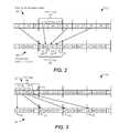
- FIG. 2depicts a first illustrative embodiment 200 of a memory structure storing pre-loaded content and additional ECC data.
- a first word line 202may include pre-loaded content, such as the pre-loaded content stored in the memory of 112 of FIG. 1 .
- the first word line 202may include four ECC pages including a first representative ECC page 206 .
- Each ECC pagemay include one or more sub-blocks, such as a first representative sub-block 212 and a second representative sub-block 214 .
- Each ECC pagemay also include main ECC data, such as representative main ECC data 218 that includes parity bits for error correction of the first sub-block 212 and the second sub-block 214 .
- a second word line 204stores additional ECC data.
- the second word line 204includes multiple ECC pages including a representative second ECC page 208 .
- Each of the ECC pages of the second word line 204includes multiple blocks of additional ECC data (e.g. additional parity) that correspond to one or more sub-blocks of the first word line 202 .
- the second representative ECC page 208includes first additional ECC data 220 , second additional ECC data 222 , third additional ECC data 224 , and fourth additional ECC data 226 .
- the second ECC page 208also includes main ECC data 228 , which provides error correction capability for errors that may occur in any of the additional ECC data 220 - 226 .
- Each of the additional ECC data 220 - 226corresponds to a sub-block of the pre-loaded content.
- a first sub-block of each of the ECC pages of the first word line 202may be individually encoded and the resulting additional parity stored in the second ECC page 208 , in a manner as illustrated and described with respect to FIG. 1 .
- the second ECC page 208includes four sets of additional ECC data 220 - 226 , and thus provides additional ECC data for the entire first word line 202 .
- the second word line 204may provide additional ECC data for data recovery for a total of four word lines that store pre-loaded content.
- one or more sub-blocks of the ECC pages of the first word line 202do not have corresponding additional parity.
- the second sub-block 214may not be protected by additional ECC data.
- the main ECC data 218may be insufficient to correct errors in the sub-blocks 212 and 214 combined, the main ECC data 218 may be sufficient to correct errors in the second sub-block 214 after the first sub-block 212 has been corrected using the second additional ECC data 222 .
- all sub-blocks of an ECC pagemay be protected using additional ECC data, as described with respect to FIG. 3 .
- FIG. 3depicts another illustrative embodiment 300 of a memory structure storing pre-loaded content and additional ECC data for the pre-loaded content.
- a first word line 302stores pre-loaded content in multiple ECC pages including a first representative ECC page 306 .
- the first ECC page 306includes four sub-blocks 310 - 316 and a main ECC data portion 318 .
- a second word line 304includes additional ECC data.
- each ECC page of the second word line 304includes four sub-blocks, with each sub-block including additional ECC data corresponding to pre-loaded content.
- a first sub-block 320 of a first page of the second word line 304provides additional ECC data for the first sub-block 310 .
- a first sub-block 322 of the second page of the second word line 304provides additional ECC data for the second sub-block 312 .
- a first sub-block 324 of a third ECC page of the second word line 304provides additional ECC data for the third sub-block 314 .
- a first sub-block 326 of a fourth ECC page of the second word line 304provides additional ECC data for the fourth sub-block 316 of the first ECC page 306 .
- FIG. 3illustrates that additional parity may be provided for individual sub-blocks of ECC pages having multiple sub-blocks of pre-loaded content.
- FIG. 3also illustrates that additional ECC data for multiple sub-blocks of a single ECC page may be stored at separate distinct ECC pages of the additional ECC data.
- the second word line 204 of FIG. 2 or the second word line 304 of FIG. 3each storing additional ECC data to aid in the data recovery of pre-loaded content, may also be protected with additional ECC data.
- errors occurring in the second ECC page 208 of FIG. 2may be correctable by applying an ECC operation using the main parity 228 . If a number of errors occurring in the second ECC page 208 exceeds an error correction capability using the main parity 228 , one or more of the sub-blocks containing the additional ECC data 220 - 226 may be provided to an ECC engine as a sub-block to be decoded using still further additional ECC parity stored in the memory in a manner similar to the second ECC operation 152 of FIG. 1 . Therefore, additional word lines may be provided to include additional parity, to enable error recovery of additional parity, which in turn enables error recovery of pre-loaded data.
- the main ECC data and the additional ECC datamay include any type of ECC data.
- the main ECC data 218 and the second additional ECC data 222may include parity bits or other redundant information according to a Bose-Chaudhuri-Hocquenghem (BCH) encoding, a Reed-Solomon encoding, a low density parity check (LDPC) encoding, or another type of encoding.
- BCHBose-Chaudhuri-Hocquenghem
- LDPClow density parity check
- the main ECC data and the additional ECC datamay use a same encoding scheme, such as a BCH scheme.
- the main ECC data and the additional ECC datamay use different encoding schemes.
- the main ECC data and the additional ECC datamay contain a same number of parity bits or may contain a different number of parity bits.
- Content datacan be stored in sectors (e.g. ECC sectors, such as the ECC page 120 of FIG. 1 ).
- the sectorsmay be organized in a word line as shown in FIGS. 2-3 .
- FIGS. 2-3illustrate organization of content data and additional ECC data in word lines, such as for a NAND flash memory array, other types of memory and other memory architectures may be used.
- Error correctionmay be a function of the number of parity bytes used in the ECC scheme.
- each word line in FIGS. 2-3may store 8 kilobytes (KB) of content data, plus parity and header data.
- Each word lineis illustrated as containing four ECC pages, and each ECC page (e.g. the first ECC page 206 ) may include 230 bytes of main ECC data (“main parity”) plus 2 KB of content data.
- main paritymain ECC data
- an error correction capability of ECC pagescould be improved by increasing a number of the main parity bits, such an increase can lead to an increase in size of a memory array (e.g. in NAND flash implementations) that may increase a cost of the memory.
- Additional paritycan be generated for a chunk, or sub-block, of the ECC page.
- the additional paritycan be generated for all of the content data.
- Each ECC pagecan include its original parity (main parity) to cover the 2 kilobytes of data and can also be associated with additional parity (e.g. of 230 bytes) to provide error detection and correction for the left-most (or right-most) half of the ECC page, such as illustrated in FIG. 2 .
- the additional paritycan be added for every quarter of the ECC page as illustrated in FIG. 3 , to both halves of the ECC page as described with respect to FIG. 1 , or according to one or more other configurations. A determination of which configuration of additional parity to use may be based on how much storage would be used for the additional parities.
- the additional paritiesmay be stored in blocks set aside to store additional parity.
- the additional parity area 162 of FIG. 1may include one or more blocks of a memory array dedicated to storing additional parity data.
- Each blockmay include multiple word lines, each word line containing one or more sectors or ECC pages of additional parity, as illustrated in FIGS. 2-3 .
- FIG. 4a particular embodiment of a method of correcting pre-loaded content in a data storage device is depicted.
- the methodis illustrated as beginning with a data storage device manufacturer pre-loading the data storage device with content 490 , additional parity 492 , and a table 494 to locate additional data, at 402 .
- the table 494may be accessible to a controller of the data storage device, such as the controller 110 of FIG. 1 , to enable the controller to locate additional parity for a particular ECC page of pre-loaded content.
- the table 494may be arranged to be indexed by a word line address and an ECC page indicator to locate an entry including a memory address or location of a corresponding additional ECC data block.
- the data storage device manufacturermay provide the pre-loaded device 404 to a host manufacturer.
- the host manufacturermay manufacture portable electronic devices that include embedded data storage devices with pre-loaded content.
- the host manufacturermay receive the pre-loaded data storage device 404 and may fasten the device 404 to a printed circuit board 406 , at 408 .
- Fastening the device 404 to the printed circuit board 406may expose the device 404 to one or more data corruption events.
- fastening the device 404may include polishing the device 404 , reflow, or one or more other events that may corrupt the pre-loaded data.
- the host manufacturermay initiate the data correction procedure, at 410 .
- the data correction proceduremay be performed by a controller of the data storage device, such as the controller 110 of FIG. 1 .
- the data correction proceduremay include decoding an ECC page of pre-loaded content using main ECC data, at 412 .
- the controller 110 of FIG. 1may be configured to start scanning the memory 112 to examine each ECC page of the pre-loaded content area 160 and to decode each ECC page using the main ECC data, such as the main ECC data 124 .
- a determinationmay be made whether the ECC page is correctable using the main ECC data, at 414 .
- the data correction proceduremay include determining whether additional pre-loaded content remains to be analyzed, at 416 .
- a next ECC page of the pre-loaded contentmay be retrieved, at 418 , and the processing returns to decode the next ECC page of the pre-loaded content using the main ECC data, at 412 .
- processingmay continue with retrieving additional parity for a sub-block of the ECC page, at 420 .
- the sub-blockmay be individually decoded, at 422 , such as illustrated and described with respect to the second ECC operation 152 of FIG. 1 .
- the ECC pagemay be updated with an error-corrected sub-block, at 424 , and processing may return to 412 , where the ECC page including the error-corrected sub-block may be decoded using the main ECC data.
- the decodingmay correspond to the third ECC operation 154 of FIG. 1 .
- the data correction proceduremay include freeing memory that contains additional parity, at 426 .
- memory locations that contain additional ECC datamay be freed by updating a file system table to indicate that the memory locations containing the additional data are unused.
- blocks containing the additional ECC datamay be erased and marked as available for storing data.
- the additional paritymay not be freed, and may be retained in the memory by the controller to enable additional ECC correction by the data storage device in case of future errors in the pre-loaded content.
- the data correction procedureis described with respect to correcting pre-loaded content after a data corrupting event occurs during manufacture, in other implementations the data correction procedure may be performed under other circumstances.
- the data correction proceduremay be used to recover user data that has been protected by additional ECC data to provide a higher error correction capability.
- the data correction procedure described with respect to FIG. 4may be a special firmware procedure may be performed by a controller or processor of the memory device.
- the proceduremay include reading each ECC page in a word line and determining if corrupted data content can be corrected with the main parity. If the data content cannot be corrected with the main parity, then the additional parity for that ECC page is retrieved and the corresponding data fields (e.g. one or more sub-blocks protected by the additional parity) will be corrected using the retrieved additional parity. After correcting the one or more sub-blocks using the additional parity, the main parity may then be used to correct the remaining errors.
- error detection and correctionmay be performed “on the fly” as content data is read from the memory instead of during a dedicated data correction procedure. Error correction may therefore be performed incrementally, as opposed to performing data correction for all pre-loaded content data in a single procedure.
- Providing additional ECC dataenables an increase of the parity for word lines without increasing a size of the memory (i.e. without increasing a size of the main ECC data 124 of FIG. 1 to accommodate additional parity bits).
- Methods of providing and using the additional ECC datamay be used with any ECC technique (e.g. BCH, Reed-Solomon, etc.).
- Enhanced error correction as described in conjunction with FIGS. 1-4may be adopted into existing controllers through firmware executed by the controllers and may be used to address corruption of preloaded content data due to soldering or other manufacturing processes.
- FIG. 5is a flowchart of a particular embodiment of a method 500 of using additional ECC data.
- the method 500may be performed in a controller of a data storage device, such as the controller 110 of FIG. 1 .
- the method 500includes receiving data including a data block and main ECC data for the data block, at 502 .
- the data blockincludes multiple sub-blocks (e.g. a first sub-block of data and a second sub-block of data).
- the controller 110may send an instruction to the memory 112 including an address of the ECC page 120 for the controller 110 to read the ECC page 120 .
- the controller 110may receive the data block corresponding to the ECC page 120 from the memory 112 .
- An ECC operation to process the data block using the main ECC datais initiated, at 504 .
- the controller 110may initiate the first ECC operation 150 of FIG. 1 to process the data block 122 using the main ECC data 124 .
- the controller 110 of FIG. 1may provide the received data block and main ECC data to an input of the ECC engine 114 .
- the controller 110may also provide a control signal to the ECC engine 114 to cause the ECC engine 114 to perform an ECC decoding operation using the data block and the main ECC data at the input of the ECC engine 114 .
- first additional ECC datathat is external to the data block is retrieved.
- the first additional ECC datacorresponds to the first sub-block of data.
- a second ECC operationis initiated to process the first sub-block of data using the first additional ECC data, at 506 .
- the controller 110may send a read instruction to the memory 112 including an address of the first additional ECC data 130 .
- the controller 110may receive the first additional ECC data 130 from the memory 112 .
- the controller 110may provide the first sub-block 126 and the first additional ECC data 130 to an input of the ECC engine 114 .
- the controller 110may also provide a control signal to the ECC engine 114 to initiate a decoding operation.
- the decoding operationmay correspond to the second ECC operation 152 of FIG. 2 .
- the data block and the main ECC datamay be retrieved as a first ECC page from a first word line of a memory, such as the first ECC page 206 of FIG. 2
- the first additional ECC datamay be retrieved from a second word line of the memory as a portion of a second ECC page, such as the second sub-block of the second ECC page 208 of FIG. 2 storing the second additional ECC data 222 .
- the second ECC pagemay include the first additional ECC data for correcting errors in the first sub-block of the first ECC page and second additional ECC data for correcting errors in the second sub-block of the first ECC page.
- the second ECC pagemay further include main parity bits, such as the main ECC data 228 of FIG. 2 , for correcting errors in the first additional ECC data and the second additional ECC data.
- the controllermay determine a location of the first additional ECC data via one or more computations, such as by applying one or more additive or multiplicative factors to a location of the data block. For example, a series of computations may be performed to map the first ECC page 206 or 306 of FIGS. 2-3 to a corresponding sub-block of the second ECC page 208 or 308 .
- a location of the first additional ECC datamay be determined by performing a table lookup operation based on a memory address of the data.
- the location of the first additional ECC datamay be further based on a location of the first sub-block within the data block.
- the controller 110may access a table that may be stored in the memory 112 of FIG. 1 or at other memory that is accessible to the controller 110 .
- the controller 110may provide an address of the data, such as an indicator of a block number and a word line number within the block for use in locating an element of the table.
- the controller 110may also provide an indication of a location of the data within the word line, such as an index of an ECC page within the word line.
- the provided location informationmay be used to locate a table element that stores a location of the first additional ECC data 130 .
- the location of the first additional ECC data 130may be retrieved from the table and used to retrieve the first additional ECC data 130 from the memory 112 .
- the ECC operation and the first sub-block ECC operationcan be performed at a common ECC engine of the data storage device, such as the ECC engine 114 of FIG. 1 that performs the first ECC operation 150 and the second ECC operation 152 .
- the ECC operation and the first sub-block ECC operationmay be performed at different ECC engines of the data storage device.
- the main ECC data and the first additional ECC datamay have a same number of parity bits.
- the main ECC datamay have a first number of parity bits and the first additional ECC data may have a second number of parity bits, the second number different from the first number.
- a third ECC operation to process the data block using the main ECC datamay be initiated, at 508 .
- the third ECC operationmay correspond to the third ECC operation 154 of FIG. 1 .
- all sub-blocks of the data blockmay be error corrected using additional ECC data and error correction using the main ECC data may be bypassed.
- the datamay correspond to pre-loaded content stored in the data storage device. Initiating the ECC operation can be performed during a data correction procedure to correct and re-store the pre-loaded content in the data storage device after a data corrupting event occurs.
- the data corrupting eventmay result from a soldering or reflow process to attach the data storage device to a printed circuit board.
- the datamay not correspond to pre-loaded content and may instead include user data that is protected by additional ECC data to provide a higher error correction capability.
- FIG. 6illustrates a particular embodiment of a method 600 of providing additional ECC data.
- the method 600may be performed in a data storage device including a memory and an error correction coding (ECC) engine, such as the memory 112 and the ECC engine 114 of the data storage device 102 of FIG. 1 .
- the method 600includes storing a first ECC page including a data block and first main ECC data to the memory, at 602 .
- the first main ECC datais usable by the ECC engine to correct errors in the first ECC page.
- the first ECC pagemay be the first ECC page 206 of FIG. 2 .
- a second ECC page including first additional ECC datais stored to the memory, at 604 .
- the first additional ECC datais usable by the ECC engine to correct errors in a single sub-block of multiple sub-blocks within the data block.
- the second ECC pagemay be the second ECC page 208 of FIG. 2 .
- a table that associates an address of the first ECC page with a location of the second ECC pagemay be stored, at 606 .
- the tablemay be stored to enable the data storage device to locate the second ECC page when a number of errors occurring in the first ECC page exceeds a correction capability of the ECC engine using the main ECC data.
- the method 600may be controlled by the data storage device manufacturer of FIG. 4 to form the pre-loaded device 404 .
- the first ECC pagemay be part of pre-loaded content stored to a first portion of the memory
- the second ECC pagemay be part of additional parity stored to a second portion of the memory.
- the pre-loaded content and the additional paritymay be stored to the memory prior to raising a temperature of the data storage device during a soldering or reflow process, such as described with respect to the host manufacturing process of FIG. 4 .
- such componentsmay include one or more microprocessors, state machines, or other circuits configured to enable the data storage device 102 of FIG. 1 to perform the particular functions attributed to such components.
- the controller 110 of FIG. 1may represent physical components, such as hardware controllers, state machines, logic circuits, or other structures, to enable the data storage device 102 to perform sub-block data correction using the additional ECC data.
- the controller 110may include dedicated hardware (i.e. circuitry) to implement error correction using additional ECC data.
- the controller 110may implement error correction using additional ECC data using a microprocessor or microcontroller programmed to determine when to retrieve and use additional ECC data to decode sub-blocks of an ECC page.
- the controller 110includes executable instructions that are executed by a processor and the instructions are stored at the memory 112 .
- executable instructions that are executed by a processor that may be included in the controller 110may be stored at a separate memory location that is not part of the memory 112 , such as at a read-only memory (ROM).
- ROMread-only memory
- the data storage device 102may be a portable device configured to be selectively coupled to one or more external devices.
- the data storage device 102may be attached or embedded within one or more host devices, such as within a housing of a portable communication device.
- the data storage device 102may be within a packaged apparatus such as a wireless telephone, personal digital assistant (PDA), gaming device or console, portable navigation device, or other device that uses internal non-volatile memory.
- PDApersonal digital assistant
- gaming device or consoleportable navigation device, or other device that uses internal non-volatile memory.
- the data storage device 102includes a non-volatile memory, such as a flash memory (e.g., NAND, NOR, Multi-Level Cell (MLC), Divided bit-line NOR (DINOR), AND, high capacitive coupling ratio (HiCR), asymmetrical contactless transistor (ACT), or other flash memories), an erasable programmable read-only memory (EPROM), an electrically-erasable programmable read-only memory (EEPROM), a read-only memory (ROM), a one-time programmable memory (OTP), or any other type of memory.
- a flash memorye.g., NAND, NOR, Multi-Level Cell (MLC), Divided bit-line NOR (DINOR), AND, high capacitive coupling ratio (HiCR), asymmetrical contactless transistor (ACT), or other flash memories
- EPROMerasable programmable read-only memory
- EEPROMelectrically-erasable programmable read-only memory
- ROMread-only memory
Landscapes
- Engineering & Computer Science (AREA)
- Theoretical Computer Science (AREA)
- Quality & Reliability (AREA)
- Physics & Mathematics (AREA)
- General Engineering & Computer Science (AREA)
- General Physics & Mathematics (AREA)
- Techniques For Improving Reliability Of Storages (AREA)
- Detection And Correction Of Errors (AREA)
Abstract
Description
Claims (19)
Priority Applications (1)
| Application Number | Priority Date | Filing Date | Title |
|---|---|---|---|
| US13/913,845US8806297B2 (en) | 2011-02-08 | 2013-06-10 | Data recovery using additional error correction coding data |
Applications Claiming Priority (2)
| Application Number | Priority Date | Filing Date | Title |
|---|---|---|---|
| US13/023,147US8484542B2 (en) | 2011-02-08 | 2011-02-08 | Data recovery using additional error correction coding data |
| US13/913,845US8806297B2 (en) | 2011-02-08 | 2013-06-10 | Data recovery using additional error correction coding data |
Related Parent Applications (1)
| Application Number | Title | Priority Date | Filing Date |
|---|---|---|---|
| US13/023,147DivisionUS8484542B2 (en) | 2011-02-08 | 2011-02-08 | Data recovery using additional error correction coding data |
Publications (2)
| Publication Number | Publication Date |
|---|---|
| US20130275832A1 US20130275832A1 (en) | 2013-10-17 |
| US8806297B2true US8806297B2 (en) | 2014-08-12 |
Family
ID=45569776
Family Applications (2)
| Application Number | Title | Priority Date | Filing Date |
|---|---|---|---|
| US13/023,147Active2031-12-27US8484542B2 (en) | 2011-02-08 | 2011-02-08 | Data recovery using additional error correction coding data |
| US13/913,845ActiveUS8806297B2 (en) | 2011-02-08 | 2013-06-10 | Data recovery using additional error correction coding data |
Family Applications Before (1)
| Application Number | Title | Priority Date | Filing Date |
|---|---|---|---|
| US13/023,147Active2031-12-27US8484542B2 (en) | 2011-02-08 | 2011-02-08 | Data recovery using additional error correction coding data |
Country Status (6)
| Country | Link |
|---|---|
| US (2) | US8484542B2 (en) |
| EP (1) | EP2673709B1 (en) |
| KR (1) | KR101394596B1 (en) |
| CN (1) | CN103329104B (en) |
| TW (1) | TW201245953A (en) |
| WO (1) | WO2012109101A1 (en) |
Cited By (7)
| Publication number | Priority date | Publication date | Assignee | Title |
|---|---|---|---|---|
| US20150106677A1 (en)* | 2013-10-15 | 2015-04-16 | International Business Machines Corporation | Handling errors in ternary content addressable memories |
| US9472270B2 (en) | 2014-10-24 | 2016-10-18 | Sandisk Technologies Llc | Nonvolatile storage reflow detection |
| US9583206B2 (en) | 2014-10-02 | 2017-02-28 | Sandisk Technologies Llc | Data storage device having reflow awareness |
| US9786386B2 (en)* | 2015-02-27 | 2017-10-10 | Microsoft Technology Licensing, Llc | Dynamic approximate storage for custom applications |
| US11500728B2 (en) | 2020-11-27 | 2022-11-15 | Samsung Electronics Co., Ltd. | Storage controller and method of restoring error of the same |
| US11831333B2 (en) | 2020-01-09 | 2023-11-28 | Microsoft Technology Licensing, Llc. | Encoding for data recovery in storage systems |
| US12266410B2 (en) | 2021-03-02 | 2025-04-01 | Micron Technology, Inc. | Methods and systems for improving ECC operation of memories |
Families Citing this family (105)
| Publication number | Priority date | Publication date | Assignee | Title |
|---|---|---|---|---|
| US8418026B2 (en)* | 2010-10-27 | 2013-04-09 | Sandisk Technologies Inc. | Hybrid error correction coding to address uncorrectable errors |
| KR101751506B1 (en)* | 2011-03-28 | 2017-06-29 | 삼성전자주식회사 | Nonvolatile memory device and management method of bad area thereof |
| US10031850B2 (en)* | 2011-06-07 | 2018-07-24 | Sandisk Technologies Llc | System and method to buffer data |
| JP5426711B2 (en)* | 2011-06-08 | 2014-02-26 | パナソニック株式会社 | MEMORY CONTROLLER AND NONVOLATILE MEMORY DEVICE |
| KR20130012737A (en)* | 2011-07-26 | 2013-02-05 | 에스케이하이닉스 주식회사 | Semiconductor memory apparatus and semiconductor system comprising the same |
| CN103197985B (en)* | 2011-11-08 | 2018-07-13 | 索尼公司 | Storage control device |
| JP2013109567A (en)* | 2011-11-21 | 2013-06-06 | Toshiba Corp | Storage device and error correction method |
| US8694862B2 (en)* | 2012-04-20 | 2014-04-08 | Arm Limited | Data processing apparatus using implicit data storage data storage and method of implicit data storage |
| JP5965076B2 (en)* | 2012-09-25 | 2016-08-03 | ヒューレット−パッカード デベロップメント カンパニー エル.ピー.Hewlett‐Packard Development Company, L.P. | Uncorrectable memory error processing method and its readable medium |
| US9059736B2 (en)* | 2012-12-03 | 2015-06-16 | Western Digital Technologies, Inc. | Methods, solid state drive controllers and data storage devices having a runtime variable raid protection scheme |
| US8904250B2 (en) | 2013-02-14 | 2014-12-02 | Micron Technology, Inc. | Autorecovery after manufacturing/system integration |
| US9367391B2 (en) | 2013-03-15 | 2016-06-14 | Micron Technology, Inc. | Error correction operations in a memory device |
| US9569308B1 (en) | 2013-07-15 | 2017-02-14 | Rambus Inc. | Reduced-overhead error detection and correction |
| JP6028709B2 (en)* | 2013-10-18 | 2016-11-16 | ソニー株式会社 | Storage control device, storage device, information processing system, and storage control method thereof |
| US9165670B2 (en)* | 2013-11-14 | 2015-10-20 | Sandisk Technologies Inc. | Data retention detection techniques for a data storage device |
| US9229806B2 (en) | 2013-11-14 | 2016-01-05 | Sandisk Technologies Inc. | Block closure techniques for a data storage device |
| US10417090B2 (en) | 2013-12-23 | 2019-09-17 | Cnex Labs, Inc. | Computing system with data protection mechanism and method of operation thereof |
| TWI544492B (en)* | 2013-12-31 | 2016-08-01 | 慧榮科技股份有限公司 | Electronic device and data management method thereof |
| CN106104491A (en)* | 2014-03-01 | 2016-11-09 | 希耐克斯实验室公司 | There is calculating system and the operational approach thereof of data protection schemes |
| US9323607B2 (en) | 2014-04-29 | 2016-04-26 | Seagate Technology Llc | Data recovery once ECC fails to correct the data |
| US9652381B2 (en)* | 2014-06-19 | 2017-05-16 | Sandisk Technologies Llc | Sub-block garbage collection |
| US10146482B2 (en) | 2014-08-01 | 2018-12-04 | Toshiba Memory Corporation | Global error recovery system |
| US10067828B2 (en)* | 2014-10-03 | 2018-09-04 | Hitachi, Ltd. | Memory controller and data control method |
| US10248497B2 (en)* | 2014-10-22 | 2019-04-02 | Advanced Micro Devices, Inc. | Error detection and correction utilizing locally stored parity information |
| KR20160059050A (en) | 2014-11-17 | 2016-05-26 | 에스케이하이닉스 주식회사 | Data storage device and operating method thereof |
| US9811420B2 (en) | 2015-03-27 | 2017-11-07 | Intel Corporation | Extracting selective information from on-die dynamic random access memory (DRAM) error correction code (ECC) |
| TWI541809B (en) | 2015-04-24 | 2016-07-11 | 群聯電子股份有限公司 | Data accessing method, memory controlling circuit unit and memory storage apparatus |
| US10063263B2 (en)* | 2015-05-20 | 2018-08-28 | International Business Machines Corporation | Extended error correction coding data storage |
| TWI575531B (en)* | 2015-08-10 | 2017-03-21 | 慧榮科技股份有限公司 | Method for accessing flash memory module and associated flash memory controller and memory device |
| US9734009B2 (en)* | 2015-10-08 | 2017-08-15 | Sandisk Technologies Llc | Data encoding techniques for a device |
| US10284232B2 (en)* | 2015-10-28 | 2019-05-07 | Pure Storage, Inc. | Dynamic error processing in a storage device |
| KR102413755B1 (en)* | 2015-11-20 | 2022-06-28 | 삼성전자주식회사 | Method of storage device to recovering performance degradation due to retention charateristic and method of data processing system including the same |
| US10152527B1 (en) | 2015-12-28 | 2018-12-11 | EMC IP Holding Company LLC | Increment resynchronization in hash-based replication |
| US9946596B2 (en) | 2016-01-29 | 2018-04-17 | Toshiba Memory Corporation | Global error recovery system |
| US10318378B2 (en) | 2016-02-25 | 2019-06-11 | Micron Technology, Inc | Redundant array of independent NAND for a three-dimensional memory array |
| US10324782B1 (en) | 2016-03-24 | 2019-06-18 | Emc Corporation | Hiccup management in a storage array |
| US10705907B1 (en) | 2016-03-24 | 2020-07-07 | EMC IP Holding Company LLC | Data protection in a heterogeneous random access storage array |
| US10101934B1 (en) | 2016-03-24 | 2018-10-16 | Emc Corporation | Memory allocation balancing for storage systems |
| US10558525B2 (en)* | 2016-06-30 | 2020-02-11 | Taiwan Semiconductor Manufacturing Company, Ltd. | Method of correcting errors in a memory array and a system for implementing the same |
| US10152371B1 (en)* | 2016-09-30 | 2018-12-11 | EMC IP Holding Company LLC | End-to-end data protection for distributed storage |
| US10223008B1 (en) | 2016-09-30 | 2019-03-05 | EMC IP Holding Company LLC | Storage array sizing for compressed applications |
| US10255172B1 (en) | 2016-09-30 | 2019-04-09 | EMC IP Holding Company LLC | Controlled testing using code error injection |
| US10079613B2 (en)* | 2016-11-18 | 2018-09-18 | SK Hynix Inc. | Data mapping scheme for generalized product codes |
| KR102844275B1 (en)* | 2017-02-02 | 2025-08-12 | 에스케이하이닉스 주식회사 | Memory system and operating method of memory system |
| US10761743B1 (en) | 2017-07-17 | 2020-09-01 | EMC IP Holding Company LLC | Establishing data reliability groups within a geographically distributed data storage environment |
| US10817388B1 (en) | 2017-07-21 | 2020-10-27 | EMC IP Holding Company LLC | Recovery of tree data in a geographically distributed environment |
| US10684780B1 (en) | 2017-07-27 | 2020-06-16 | EMC IP Holding Company LLC | Time sensitive data convolution and de-convolution |
| US10880040B1 (en) | 2017-10-23 | 2020-12-29 | EMC IP Holding Company LLC | Scale-out distributed erasure coding |
| US10528260B1 (en) | 2017-10-26 | 2020-01-07 | EMC IP Holding Company LLC | Opportunistic ‘XOR’ of data for geographically diverse storage |
| US20190196726A1 (en)* | 2017-12-26 | 2019-06-27 | Nanya Technology Corporation | Dynamic random access memory and method of operating the same |
| CN108052414B (en)* | 2017-12-28 | 2021-09-17 | 湖南国科微电子股份有限公司 | Method and system for improving working temperature range of SSD |
| US10382554B1 (en) | 2018-01-04 | 2019-08-13 | Emc Corporation | Handling deletes with distributed erasure coding |
| KR102432551B1 (en)* | 2018-02-13 | 2022-08-16 | 삼성전자주식회사 | Semiconductor memory devices, memory systems including the same and methods of operating semiconductor memory devices |
| US10817374B2 (en) | 2018-04-12 | 2020-10-27 | EMC IP Holding Company LLC | Meta chunks |
| US10579297B2 (en) | 2018-04-27 | 2020-03-03 | EMC IP Holding Company LLC | Scaling-in for geographically diverse storage |
| US11023130B2 (en) | 2018-06-15 | 2021-06-01 | EMC IP Holding Company LLC | Deleting data in a geographically diverse storage construct |
| US10936196B2 (en) | 2018-06-15 | 2021-03-02 | EMC IP Holding Company LLC | Data convolution for geographically diverse storage |
| US10719250B2 (en)* | 2018-06-29 | 2020-07-21 | EMC IP Holding Company LLC | System and method for combining erasure-coded protection sets |
| US10795759B2 (en) | 2018-09-10 | 2020-10-06 | Micron Technology, Inc. | Apparatuses and methods for error correction coding and data bus inversion for semiconductor memories |
| KR102766573B1 (en)* | 2018-09-21 | 2025-02-12 | 삼성전자주식회사 | Memory device and memory system having multiple error correction function and operating method thereof |
| KR102719499B1 (en) | 2018-10-15 | 2024-10-21 | 에스케이하이닉스 주식회사 | Error correction circuit, memory controller having the error correction circuit, and memory system having the memory controller |
| US11436203B2 (en) | 2018-11-02 | 2022-09-06 | EMC IP Holding Company LLC | Scaling out geographically diverse storage |
| US10901635B2 (en) | 2018-12-04 | 2021-01-26 | EMC IP Holding Company LLC | Mapped redundant array of independent nodes for data storage with high performance using logical columns of the nodes with different widths and different positioning patterns |
| US11119683B2 (en) | 2018-12-20 | 2021-09-14 | EMC IP Holding Company LLC | Logical compaction of a degraded chunk in a geographically diverse data storage system |
| US10931777B2 (en) | 2018-12-20 | 2021-02-23 | EMC IP Holding Company LLC | Network efficient geographically diverse data storage system employing degraded chunks |
| US10892782B2 (en) | 2018-12-21 | 2021-01-12 | EMC IP Holding Company LLC | Flexible system and method for combining erasure-coded protection sets |
| US10768840B2 (en) | 2019-01-04 | 2020-09-08 | EMC IP Holding Company LLC | Updating protection sets in a geographically distributed storage environment |
| US11023331B2 (en) | 2019-01-04 | 2021-06-01 | EMC IP Holding Company LLC | Fast recovery of data in a geographically distributed storage environment |
| US10942827B2 (en) | 2019-01-22 | 2021-03-09 | EMC IP Holding Company LLC | Replication of data in a geographically distributed storage environment |
| US10846003B2 (en) | 2019-01-29 | 2020-11-24 | EMC IP Holding Company LLC | Doubly mapped redundant array of independent nodes for data storage |
| US10936239B2 (en) | 2019-01-29 | 2021-03-02 | EMC IP Holding Company LLC | Cluster contraction of a mapped redundant array of independent nodes |
| US10942825B2 (en) | 2019-01-29 | 2021-03-09 | EMC IP Holding Company LLC | Mitigating real node failure in a mapped redundant array of independent nodes |
| US10866766B2 (en) | 2019-01-29 | 2020-12-15 | EMC IP Holding Company LLC | Affinity sensitive data convolution for data storage systems |
| KR102851230B1 (en) | 2019-02-14 | 2025-08-27 | 에스케이하이닉스 주식회사 | Memory controller |
| US10983883B2 (en) | 2019-03-27 | 2021-04-20 | Spin Memory, Inc. | Error recovery in magnetic random access memory after reflow soldering |
| US11029865B2 (en) | 2019-04-03 | 2021-06-08 | EMC IP Holding Company LLC | Affinity sensitive storage of data corresponding to a mapped redundant array of independent nodes |
| US10944826B2 (en) | 2019-04-03 | 2021-03-09 | EMC IP Holding Company LLC | Selective instantiation of a storage service for a mapped redundant array of independent nodes |
| US11119686B2 (en) | 2019-04-30 | 2021-09-14 | EMC IP Holding Company LLC | Preservation of data during scaling of a geographically diverse data storage system |
| US11121727B2 (en) | 2019-04-30 | 2021-09-14 | EMC IP Holding Company LLC | Adaptive data storing for data storage systems employing erasure coding |
| US11113146B2 (en) | 2019-04-30 | 2021-09-07 | EMC IP Holding Company LLC | Chunk segment recovery via hierarchical erasure coding in a geographically diverse data storage system |
| US11748004B2 (en) | 2019-05-03 | 2023-09-05 | EMC IP Holding Company LLC | Data replication using active and passive data storage modes |
| US11209996B2 (en) | 2019-07-15 | 2021-12-28 | EMC IP Holding Company LLC | Mapped cluster stretching for increasing workload in a data storage system |
| US11449399B2 (en) | 2019-07-30 | 2022-09-20 | EMC IP Holding Company LLC | Mitigating real node failure of a doubly mapped redundant array of independent nodes |
| US11023145B2 (en) | 2019-07-30 | 2021-06-01 | EMC IP Holding Company LLC | Hybrid mapped clusters for data storage |
| KR20210015087A (en) | 2019-07-31 | 2021-02-10 | 에스케이하이닉스 주식회사 | Error correction circuit, memory controller having the error correction circuit, and memory system having the memory controller |
| US11228322B2 (en) | 2019-09-13 | 2022-01-18 | EMC IP Holding Company LLC | Rebalancing in a geographically diverse storage system employing erasure coding |
| US11449248B2 (en) | 2019-09-26 | 2022-09-20 | EMC IP Holding Company LLC | Mapped redundant array of independent data storage regions |
| US11435910B2 (en) | 2019-10-31 | 2022-09-06 | EMC IP Holding Company LLC | Heterogeneous mapped redundant array of independent nodes for data storage |
| US11288139B2 (en) | 2019-10-31 | 2022-03-29 | EMC IP Holding Company LLC | Two-step recovery employing erasure coding in a geographically diverse data storage system |
| US11119690B2 (en) | 2019-10-31 | 2021-09-14 | EMC IP Holding Company LLC | Consolidation of protection sets in a geographically diverse data storage environment |
| US11435957B2 (en) | 2019-11-27 | 2022-09-06 | EMC IP Holding Company LLC | Selective instantiation of a storage service for a doubly mapped redundant array of independent nodes |
| US11144220B2 (en) | 2019-12-24 | 2021-10-12 | EMC IP Holding Company LLC | Affinity sensitive storage of data corresponding to a doubly mapped redundant array of independent nodes |
| US11231860B2 (en) | 2020-01-17 | 2022-01-25 | EMC IP Holding Company LLC | Doubly mapped redundant array of independent nodes for data storage with high performance |
| US11507308B2 (en) | 2020-03-30 | 2022-11-22 | EMC IP Holding Company LLC | Disk access event control for mapped nodes supported by a real cluster storage system |
| US11218165B2 (en)* | 2020-05-15 | 2022-01-04 | Alibaba Group Holding Limited | Memory-mapped two-dimensional error correction code for multi-bit error tolerance in DRAM |
| US11288229B2 (en) | 2020-05-29 | 2022-03-29 | EMC IP Holding Company LLC | Verifiable intra-cluster migration for a chunk storage system |
| US11043266B1 (en) | 2020-06-15 | 2021-06-22 | Western Digital Technologies, Inc. | Multi-level read after heating event in non-volatile storage |
| US11693983B2 (en) | 2020-10-28 | 2023-07-04 | EMC IP Holding Company LLC | Data protection via commutative erasure coding in a geographically diverse data storage system |
| US11468963B2 (en)* | 2020-12-08 | 2022-10-11 | Macronix International Co., Ltd. | Memory device and read method thereof |
| US11847141B2 (en) | 2021-01-19 | 2023-12-19 | EMC IP Holding Company LLC | Mapped redundant array of independent nodes employing mapped reliability groups for data storage |
| US11625174B2 (en) | 2021-01-20 | 2023-04-11 | EMC IP Holding Company LLC | Parity allocation for a virtual redundant array of independent disks |
| US11449234B1 (en) | 2021-05-28 | 2022-09-20 | EMC IP Holding Company LLC | Efficient data access operations via a mapping layer instance for a doubly mapped redundant array of independent nodes |
| US11354191B1 (en) | 2021-05-28 | 2022-06-07 | EMC IP Holding Company LLC | Erasure coding in a large geographically diverse data storage system |
| KR20230026016A (en)* | 2021-08-17 | 2023-02-24 | 삼성전자주식회사 | Storage devices |
| US11994947B2 (en)* | 2022-08-09 | 2024-05-28 | Micron Technology, Inc. | Multi-layer code rate architecture for special event protection with reduced performance penalty |
Citations (26)
| Publication number | Priority date | Publication date | Assignee | Title |
|---|---|---|---|---|
| US5901159A (en) | 1995-12-25 | 1999-05-04 | Sony Corporation | Apparatus and method for decoding a coded digital signal |
| US5978958A (en)* | 1995-04-03 | 1999-11-02 | Matsushita Electric Industrial Co., Ltd. | Data transmission system, data recording and reproducing apparatus and recording medium each having data structure of error correcting code |
| US6092231A (en) | 1998-06-12 | 2000-07-18 | Qlogic Corporation | Circuit and method for rapid checking of error correction codes using cyclic redundancy check |
| US6651212B1 (en) | 1999-12-16 | 2003-11-18 | Hitachi, Ltd. | Recording/reproduction device, semiconductor memory, and memory card using the semiconductor memory |
| US6757862B1 (en)* | 2000-08-21 | 2004-06-29 | Handspring, Inc. | Method and apparatus for digital data error correction coding |
| US20050091569A1 (en) | 2003-10-24 | 2005-04-28 | Hon Hai Precision Industry Co., Ltd. | System and method for securely storing data in a memory |
| US7171591B2 (en) | 2003-12-23 | 2007-01-30 | International Business Machines Corporation | Method and apparatus for encoding special uncorrectable errors in an error correction code |
| US7173852B2 (en) | 2003-10-03 | 2007-02-06 | Sandisk Corporation | Corrected data storage and handling methods |
| US20070157064A1 (en) | 2005-12-27 | 2007-07-05 | D.S.P. Group Ltd. | Systems and methods for error corrections |
| US20080168319A1 (en) | 2007-01-08 | 2008-07-10 | Samsung Electronics Co., Ltd. | Flash memory Device Error Correction Code Controllers and Related Methods and Memory Systems |
| US20080256420A1 (en) | 2007-04-12 | 2008-10-16 | International Business Machines Corporation | Error checking addressable blocks in storage |
| US20090013233A1 (en) | 2007-07-06 | 2009-01-08 | Micron Technology, Inc. | Error recovery storage along a nand-flash string |
| US7518919B2 (en) | 2003-10-03 | 2009-04-14 | Sandisk Corporation | Flash memory data correction and scrub techniques |
| US20090292970A1 (en) | 2008-05-23 | 2009-11-26 | Chun Fung Man | Using error information from nearby locations to recover uncorrectable data in non-volatile memory |
| US7747903B2 (en)* | 2007-07-09 | 2010-06-29 | Micron Technology, Inc. | Error correction for memory |
| US7809994B2 (en)* | 2006-05-17 | 2010-10-05 | Sandisk Corporation | Error correction coding for multiple-sector pages in flash memory devices |
| US7849381B2 (en) | 2004-12-21 | 2010-12-07 | Sandisk Corporation | Method for copying data in reprogrammable non-volatile memory |
| US7859931B2 (en)* | 2007-12-14 | 2010-12-28 | Hynix Semiconductor Inc. | Refresh period signal generator with digital temperature information generation function |
| US7898862B2 (en)* | 2004-10-25 | 2011-03-01 | Kabushiki Kaisha Toshiba | Memory card, semiconductor device, and method of controlling memory card |
| US7900117B2 (en)* | 2007-09-26 | 2011-03-01 | Kabushiki Kaisha Toshiba | Semiconductor memory device and its control method |
| US7958427B1 (en) | 2007-03-30 | 2011-06-07 | Link—A—Media Devices Corporation | ECC with out of order completion |
| US8095851B2 (en) | 2007-09-06 | 2012-01-10 | Siliconsystems, Inc. | Storage subsystem capable of adjusting ECC settings based on monitored conditions |
| US8098537B2 (en)* | 2008-12-18 | 2012-01-17 | Sandisk Technologies Inc. | Data refresh for non-volatile storage |
| US8136008B1 (en) | 2007-03-30 | 2012-03-13 | Link—A—Media Devices Corporation | ECC with out of order completion |
| US8234541B2 (en)* | 2007-09-07 | 2012-07-31 | Artek Microelectronics Co., Ltd. | Method and controller for data access in a flash memory |
| US8245101B2 (en) | 2007-12-27 | 2012-08-14 | Sandisk Enterprise Ip Llc | Patrol function used in flash storage controller to detect data errors |
- 2011
- 2011-02-08USUS13/023,147patent/US8484542B2/enactiveActive
- 2012
- 2012-02-03EPEP12703224.1Apatent/EP2673709B1/enactiveActive
- 2012-02-03WOPCT/US2012/023735patent/WO2012109101A1/enactiveApplication Filing
- 2012-02-03CNCN201280005978.6Apatent/CN103329104B/ennot_activeExpired - Fee Related
- 2012-02-03KRKR1020137021030Apatent/KR101394596B1/ennot_activeExpired - Fee Related
- 2012-02-07TWTW101103943Apatent/TW201245953A/enunknown
- 2013
- 2013-06-10USUS13/913,845patent/US8806297B2/enactiveActive
Patent Citations (28)
| Publication number | Priority date | Publication date | Assignee | Title |
|---|---|---|---|---|
| US5978958A (en)* | 1995-04-03 | 1999-11-02 | Matsushita Electric Industrial Co., Ltd. | Data transmission system, data recording and reproducing apparatus and recording medium each having data structure of error correcting code |
| US6397366B1 (en)* | 1995-04-03 | 2002-05-28 | Matsushita Electric Industrial Co., Ltd. | Data transmission system, data recording and reproducing apparatus and recording medium each having data structure of error correcting code |
| US5901159A (en) | 1995-12-25 | 1999-05-04 | Sony Corporation | Apparatus and method for decoding a coded digital signal |
| US6092231A (en) | 1998-06-12 | 2000-07-18 | Qlogic Corporation | Circuit and method for rapid checking of error correction codes using cyclic redundancy check |
| US6651212B1 (en) | 1999-12-16 | 2003-11-18 | Hitachi, Ltd. | Recording/reproduction device, semiconductor memory, and memory card using the semiconductor memory |
| US6757862B1 (en)* | 2000-08-21 | 2004-06-29 | Handspring, Inc. | Method and apparatus for digital data error correction coding |
| US7173852B2 (en) | 2003-10-03 | 2007-02-06 | Sandisk Corporation | Corrected data storage and handling methods |
| US7518919B2 (en) | 2003-10-03 | 2009-04-14 | Sandisk Corporation | Flash memory data correction and scrub techniques |
| US20050091569A1 (en) | 2003-10-24 | 2005-04-28 | Hon Hai Precision Industry Co., Ltd. | System and method for securely storing data in a memory |
| US7171591B2 (en) | 2003-12-23 | 2007-01-30 | International Business Machines Corporation | Method and apparatus for encoding special uncorrectable errors in an error correction code |
| US7898862B2 (en)* | 2004-10-25 | 2011-03-01 | Kabushiki Kaisha Toshiba | Memory card, semiconductor device, and method of controlling memory card |
| US7849381B2 (en) | 2004-12-21 | 2010-12-07 | Sandisk Corporation | Method for copying data in reprogrammable non-volatile memory |
| US20070157064A1 (en) | 2005-12-27 | 2007-07-05 | D.S.P. Group Ltd. | Systems and methods for error corrections |
| US7809994B2 (en)* | 2006-05-17 | 2010-10-05 | Sandisk Corporation | Error correction coding for multiple-sector pages in flash memory devices |
| US20080168319A1 (en) | 2007-01-08 | 2008-07-10 | Samsung Electronics Co., Ltd. | Flash memory Device Error Correction Code Controllers and Related Methods and Memory Systems |
| US7958427B1 (en) | 2007-03-30 | 2011-06-07 | Link—A—Media Devices Corporation | ECC with out of order completion |
| US8136008B1 (en) | 2007-03-30 | 2012-03-13 | Link—A—Media Devices Corporation | ECC with out of order completion |
| US20080256420A1 (en) | 2007-04-12 | 2008-10-16 | International Business Machines Corporation | Error checking addressable blocks in storage |
| US20090013233A1 (en) | 2007-07-06 | 2009-01-08 | Micron Technology, Inc. | Error recovery storage along a nand-flash string |
| US7747903B2 (en)* | 2007-07-09 | 2010-06-29 | Micron Technology, Inc. | Error correction for memory |
| US7996727B2 (en)* | 2007-07-09 | 2011-08-09 | Micron Technology, Inc. | Error correction for memory |
| US8095851B2 (en) | 2007-09-06 | 2012-01-10 | Siliconsystems, Inc. | Storage subsystem capable of adjusting ECC settings based on monitored conditions |
| US8234541B2 (en)* | 2007-09-07 | 2012-07-31 | Artek Microelectronics Co., Ltd. | Method and controller for data access in a flash memory |
| US7900117B2 (en)* | 2007-09-26 | 2011-03-01 | Kabushiki Kaisha Toshiba | Semiconductor memory device and its control method |
| US7859931B2 (en)* | 2007-12-14 | 2010-12-28 | Hynix Semiconductor Inc. | Refresh period signal generator with digital temperature information generation function |
| US8245101B2 (en) | 2007-12-27 | 2012-08-14 | Sandisk Enterprise Ip Llc | Patrol function used in flash storage controller to detect data errors |
| US20090292970A1 (en) | 2008-05-23 | 2009-11-26 | Chun Fung Man | Using error information from nearby locations to recover uncorrectable data in non-volatile memory |
| US8098537B2 (en)* | 2008-12-18 | 2012-01-17 | Sandisk Technologies Inc. | Data refresh for non-volatile storage |
Non-Patent Citations (5)
| Title |
|---|
| International Preliminary Report on Patentability for International Application No. PCT/US2012/023735, issued Aug. 13, 2013, 6 pages. |
| Notice of Allowance and Fee(s) Due mailed Mar. 14, 2013 in U.S. Appl. No. 13/023,147, 15 pages. |
| Office Action mailed Sep. 24, 2013 in Korean Application No. 10-2013-7021030 with English translation, 8 pages. |
| Supplemental Notice of Allowability mailed Apr. 18, 2013 in U.S. Appl. No. 13/023,147, 12 pages. |
| The International Search Report and Written Opinion mailed Apr. 23, 2012 in International Application No. PCT/US2012/023735, 11 pages. |
Cited By (10)
| Publication number | Priority date | Publication date | Assignee | Title |
|---|---|---|---|---|
| US20150106677A1 (en)* | 2013-10-15 | 2015-04-16 | International Business Machines Corporation | Handling errors in ternary content addressable memories |
| US20150106676A1 (en)* | 2013-10-15 | 2015-04-16 | International Business Machines Corporation | Handling errors in ternary content addressable memories |
| US9213596B2 (en)* | 2013-10-15 | 2015-12-15 | International Business Machines Corporation | Handling errors in ternary content addressable memories |
| US9213595B2 (en)* | 2013-10-15 | 2015-12-15 | International Business Machines Corporation | Handling errors in ternary content addressable memories |
| US9583206B2 (en) | 2014-10-02 | 2017-02-28 | Sandisk Technologies Llc | Data storage device having reflow awareness |
| US9472270B2 (en) | 2014-10-24 | 2016-10-18 | Sandisk Technologies Llc | Nonvolatile storage reflow detection |
| US9786386B2 (en)* | 2015-02-27 | 2017-10-10 | Microsoft Technology Licensing, Llc | Dynamic approximate storage for custom applications |
| US11831333B2 (en) | 2020-01-09 | 2023-11-28 | Microsoft Technology Licensing, Llc. | Encoding for data recovery in storage systems |
| US11500728B2 (en) | 2020-11-27 | 2022-11-15 | Samsung Electronics Co., Ltd. | Storage controller and method of restoring error of the same |
| US12266410B2 (en) | 2021-03-02 | 2025-04-01 | Micron Technology, Inc. | Methods and systems for improving ECC operation of memories |
Also Published As
| Publication number | Publication date |
|---|---|
| TW201245953A (en) | 2012-11-16 |
| EP2673709B1 (en) | 2019-06-12 |
| US20130275832A1 (en) | 2013-10-17 |
| WO2012109101A1 (en) | 2012-08-16 |
| US20120204077A1 (en) | 2012-08-09 |
| CN103329104A (en) | 2013-09-25 |
| CN103329104B (en) | 2016-08-10 |
| KR101394596B1 (en) | 2014-05-14 |
| KR20130101149A (en) | 2013-09-12 |
| EP2673709A1 (en) | 2013-12-18 |
| US8484542B2 (en) | 2013-07-09 |
Similar Documents
| Publication | Publication Date | Title |
|---|---|---|
| US8806297B2 (en) | Data recovery using additional error correction coding data | |
| US8418026B2 (en) | Hybrid error correction coding to address uncorrectable errors | |
| US9043678B2 (en) | Detecting effect of corrupting event on preloaded data in non-volatile memory | |
| US9124300B2 (en) | Error correction coding in non-volatile memory | |
| US8719677B2 (en) | Using ECC encoding to verify an ECC decode operation | |
| JP5675954B2 (en) | Detection of irregular parity distribution via metadata tag | |
| US8635510B2 (en) | Non-systematic coded error correction | |
| US9244767B1 (en) | Data storage device with in-memory parity circuitry | |
| CN109426580A (en) | Data storage device and its operating method | |
| US9229801B2 (en) | Method and device for write abort protection | |
| US20150046772A1 (en) | Method and device for error correcting code (ecc) error handling | |
| US9129689B2 (en) | Tracking erase pulses for non-volatile memory | |
| TW201351425A (en) | System and method to decode data subject to a disturb condition | |
| WO2013138115A1 (en) | Statistical distribution based variable-bit error correction coding | |
| WO2013126182A1 (en) | Erasure correction using single error detection parity | |
| US20100287448A1 (en) | Flash memory device with rectifiable redundancy bit and method of controlling the same | |
| US9117533B2 (en) | Tracking erase operations to regions of non-volatile memory | |
| US20130047056A1 (en) | Flash memory device with rectifiable redundancy and method of controlling the same | |
| US20250123922A1 (en) | Non-Blocking Chipkill Recovery | |
| CN119025020A (en) | Data access management method, memory controller of memory device, memory device and electronic device | |
| US9223649B2 (en) | System and method of sending correction data to a buffer of a non-volatile memory |
Legal Events
| Date | Code | Title | Description |
|---|---|---|---|
| AS | Assignment | Owner name:SANDISK TECHNOLOGIES INC., TEXAS Free format text:ASSIGNMENT OF ASSIGNORS INTEREST;ASSIGNORS:D'ABREU, MANUEL ANTONIO;SKALA, STEPHEN;REEL/FRAME:030578/0708 Effective date:20130606 | |
| STCF | Information on status: patent grant | Free format text:PATENTED CASE | |
| AS | Assignment | Owner name:SANDISK TECHNOLOGIES LLC, TEXAS Free format text:CHANGE OF NAME;ASSIGNOR:SANDISK TECHNOLOGIES INC;REEL/FRAME:038807/0948 Effective date:20160516 | |
| MAFP | Maintenance fee payment | Free format text:PAYMENT OF MAINTENANCE FEE, 4TH YEAR, LARGE ENTITY (ORIGINAL EVENT CODE: M1551) Year of fee payment:4 | |
| MAFP | Maintenance fee payment | Free format text:PAYMENT OF MAINTENANCE FEE, 8TH YEAR, LARGE ENTITY (ORIGINAL EVENT CODE: M1552); ENTITY STATUS OF PATENT OWNER: LARGE ENTITY Year of fee payment:8 | |
| AS | Assignment | Owner name:SANDISK TECHNOLOGIES, INC., CALIFORNIA Free format text:ASSIGNMENT OF ASSIGNORS INTEREST;ASSIGNOR:SANDISK TECHNOLOGIES LLC;REEL/FRAME:069796/0423 Effective date:20241227 | |
| AS | Assignment | Owner name:SANDISK TECHNOLOGIES, INC., CALIFORNIA Free format text:PARTIAL RELEASE OF SECURITY INTERESTS;ASSIGNOR:JPMORGAN CHASE BANK, N.A., AS AGENT;REEL/FRAME:071382/0001 Effective date:20250424 Owner name:JPMORGAN CHASE BANK, N.A., AS COLLATERAL AGENT, ILLINOIS Free format text:SECURITY AGREEMENT;ASSIGNOR:SANDISK TECHNOLOGIES, INC.;REEL/FRAME:071050/0001 Effective date:20250424 |