US8806152B2 - Method and apparatus for sending data from multiple sources over a communications bus - Google Patents
Method and apparatus for sending data from multiple sources over a communications busDownload PDFInfo
- Publication number
- US8806152B2 US8806152B2US13/692,269US201213692269AUS8806152B2US 8806152 B2US8806152 B2US 8806152B2US 201213692269 AUS201213692269 AUS 201213692269AUS 8806152 B2US8806152 B2US 8806152B2
- Authority
- US
- United States
- Prior art keywords
- data
- source
- section
- source data
- lane
- Prior art date
- Legal status (The legal status is an assumption and is not a legal conclusion. Google has not performed a legal analysis and makes no representation as to the accuracy of the status listed.)
- Expired - Lifetime
Links
Images


Classifications
- G—PHYSICS
- G06—COMPUTING OR CALCULATING; COUNTING
- G06F—ELECTRIC DIGITAL DATA PROCESSING
- G06F13/00—Interconnection of, or transfer of information or other signals between, memories, input/output devices or central processing units
- G06F13/14—Handling requests for interconnection or transfer
- G06F13/16—Handling requests for interconnection or transfer for access to memory bus
- G06F13/1605—Handling requests for interconnection or transfer for access to memory bus based on arbitration
- G06F13/161—Handling requests for interconnection or transfer for access to memory bus based on arbitration with latency improvement
- G—PHYSICS
- G06—COMPUTING OR CALCULATING; COUNTING
- G06F—ELECTRIC DIGITAL DATA PROCESSING
- G06F13/00—Interconnection of, or transfer of information or other signals between, memories, input/output devices or central processing units
- G06F13/14—Handling requests for interconnection or transfer
- G06F13/16—Handling requests for interconnection or transfer for access to memory bus
- G—PHYSICS
- G06—COMPUTING OR CALCULATING; COUNTING
- G06F—ELECTRIC DIGITAL DATA PROCESSING
- G06F12/00—Accessing, addressing or allocating within memory systems or architectures
- G—PHYSICS
- G06—COMPUTING OR CALCULATING; COUNTING
- G06F—ELECTRIC DIGITAL DATA PROCESSING
- G06F13/00—Interconnection of, or transfer of information or other signals between, memories, input/output devices or central processing units
- G—PHYSICS
- G06—COMPUTING OR CALCULATING; COUNTING
- G06F—ELECTRIC DIGITAL DATA PROCESSING
- G06F13/00—Interconnection of, or transfer of information or other signals between, memories, input/output devices or central processing units
- G06F13/38—Information transfer, e.g. on bus
- G06F13/40—Bus structure
- G06F13/4004—Coupling between buses
- G06F13/4009—Coupling between buses with data restructuring
- G06F13/4013—Coupling between buses with data restructuring with data re-ordering, e.g. Endian conversion
- G—PHYSICS
- G06—COMPUTING OR CALCULATING; COUNTING
- G06F—ELECTRIC DIGITAL DATA PROCESSING
- G06F13/00—Interconnection of, or transfer of information or other signals between, memories, input/output devices or central processing units
- G06F13/38—Information transfer, e.g. on bus
- G06F13/42—Bus transfer protocol, e.g. handshake; Synchronisation
- G06F13/4247—Bus transfer protocol, e.g. handshake; Synchronisation on a daisy chain bus
- G—PHYSICS
- G06—COMPUTING OR CALCULATING; COUNTING
- G06F—ELECTRIC DIGITAL DATA PROCESSING
- G06F2213/00—Indexing scheme relating to interconnection of, or transfer of information or other signals between, memories, input/output devices or central processing units
- G06F2213/16—Memory access
Definitions
- a computer system 100may include a processor 102 , a memory controller 104 , and main memory storage 106 .
- Main memory storage 106includes one or more memory chips, such as Dynamic Random Access Memory (DRAM) chips.
- DRAMDynamic Random Access Memory
- the processor 102sends a data request to the memory controller 104 over a communications bus 108 .
- Memory controller 104processes and reformats the request, and sends one or more reformatted request messages to main memory storage 106 over a main memory storage bus 110 .
- Main memory storage 106then returns the requested data to memory controller 104 over the main memory storage bus 110 .
- memory controller 104then sends the data to processor 102 over the data communications bus 108 .
- memory controller 104could be processing multiple transactions simultaneously. This can result in a situation where data from multiple sources (e.g., multiple DRAMs within main memory storage 106 ) are simultaneously available to be returned from main memory storage 106 to the memory controller 104 over the main memory storage bus 110 . When this occurs, memory controller 104 performs an arbitration process to determine which source (e.g., which DRAM) will be granted access to the main memory storage bus 110 .
- sourcese.g., multiple DRAMs within main memory storage 106
- main memory storage 106places the data associated with a transaction on the main memory storage bus 110 for one or more bus clock cycles, depending on the size of the transaction and the width of the main memory storage bus 110 (e.g., the number of parallel bits). For example, if a transaction includes 52 data bits, and the bus width is 32 bits, two clock cycles would be used to transfer the data on the bus 110 . Assuming, for simplicity, that no header information is included, the first 32 bits could be transferred during a first clock cycle, and the last 20 bits could be transferred during a second clock cycle.
- the above exampleillustrates that, during the last clock cycle in which a transaction's data is being transferred on the main memory storage bus 110 , the bus 110 often is not completely filled. In this example, only 20 of the 32 available bits are filled during the second clock cycle, leaving 12 bits empty. In current systems, if the main memory storage bus 110 will be granted to another source (e.g., another DRAM) upon the completion of the transaction, these 12 bits would be left empty, and the data for the next transaction would start on the next clock cycle.
- another sourcee.g., another DRAM
- the exampleillustrates that gaps inherently exist on the main memory storage bus 110 , using prior art techniques. These gaps result in increased system latency and decreased bandwidth.
- an electronic systemincludes a processor, which generates and sends one or more memory access requests, and multiple memory modules.
- the memory modulesare operatively coupled together through a communications bus, and they return data requested in the one or more memory access requests.
- Each of the multiple memory modulesis a data source, and a memory module of the multiple memory modules determines that first source data and second source data are available. It also allocates one or more first contiguous lanes within a first section of a data block to at least some of the first source data, where the data block includes a set of multiple lanes, and each lane includes a set of configurable bits, and allocates one or more second contiguous lanes within a second section of the data block to at least some of the second source data.
- the second sectionbegins at a next lane, which is contiguous with the first section.
- the memory modulealso sends, over the communications bus and during a data block transmission period, at least a portion of the first source data within the first section of the data block, and at least a portion of the second source data within the second section of the data block.
- a memory moduleincludes one or more memory storage units for storing local data, and a hub, operatively coupled to the one or more memory storage units and to a communications bus over which the hub can receive downstream data from one or more other hubs.
- the hubdetermines that first source data and second source data are available.
- the hubalso allocates one or more first contiguous lanes within a first section of a data block to at least some of the first source data, where the data block includes a set of multiple lanes, and each lane includes a set of configurable bits, and allocates one or more second contiguous lanes within a second section of the data block to at least some of the second source data, where the second section begins at a next lane, which is contiguous with the first section.
- the hubalso sends, over the communications bus and during a data block transmission period, at least a portion of the first source data within the first section of the data block, and at least a portion of the second source data within the second section of the data block.
- an apparatus for assembling and sending dataincludes means for receiving local data from one or more memory storage units, means for receiving downstream data over a communications bus from one or more downstream data sources, and means for making a determination of how the local data and the downstream data will be sent over the communications bus. Making the determination includes allocating one or more first contiguous lanes within a first section of a data block to at least some of the local data, where the data block includes a set of multiple lanes, and each lane includes a set of configurable bits, and allocating one or more second contiguous lanes within a second section of the data block to at least some of the downstream data, where the first section and the second section are contiguous.
- an apparatus for sending data over a communications busincludes means for receiving first source data from a first data source, means for receiving second source data from a second data source, and means for sending the first source data and the second source data over the communications bus.
- Sending the first source data and the second source dataincludes sending the first source data over the communications bus, identifying a first breakpoint corresponding to an end of the first source data, sending the second source data over the communications bus contiguously with the end of the first source data, and identifying a second breakpoint corresponding to an end of the second source data.
- a method for sending data on a communications busincludes arranging a first portion of first source data within a data block structure during a first processing period, where the data block structure includes a fixed number of contiguous, configurable bits, and sending the first portion of the first source data over the communications bus.
- the methodfurther includes arranging a remainder portion of the first source data within a first section of the data block structure during a second processing period, where the first section includes a first set of contiguous bits, arranging a first portion of second source data within a second section of the data block structure during the second processing period, where the second section is contiguous with the first section, and the second section includes a second set of contiguous bits, and sending the remainder portion of the first source data and the first portion of the second source data.
- a methodincludes determining that first source data and second source data are available, and allocating one or more first contiguous lanes within a first section of a data block to at least some of the first source data, where the data block includes a set of multiple lanes, and each lane includes a set of configurable bits.
- the methodfurther includes allocating one or more second contiguous lanes within a second section of the data block to at least some of the second source data, where the second section begins at a next lane, which is contiguous with the first section, and sending, over a communications bus and during a data block transmission period, at least a portion of the first source data within the first section of the data block, and at least a portion of the second source data within the second section of the data block.
- a methodin a further embodiment, includes arranging first source data from a first source within a first section of a data block structure, where the data block structure includes a fixed number of contiguous, configurable bits, and data within the data block structure is periodically sent out on a communications bus. The method further includes determining that second source data from a second source is available to be sent over the communications bus, and requesting access to the communications bus to send the second source data.
- the methodfurther includes receiving an indication of where, within the data block structure, at least a portion of the second source data should be placed, arranging at least a portion of the second source data within the data block structure according to the indication, resulting in at least a portion of the second source data occupying a second section of the data block that is contiguous with an end of the first section, and sending the first source data and at least a portion of the second source data over the communications bus during a data block transmission period.
- a methodin a further embodiment, includes arranging first source data within a first section of a data block structure, where the data block structure includes fixed number of contiguous, configurable bits. The method further includes receiving a request to send second source data over the communications bus, identifying a location of a breakpoint in the first source data, and arranging at least a portion of the second source data within a second section of the data block structure after the breakpoint, where the second section is contiguous with an end of the first section. The method further includes sending the first source data and at least a portion of the second source data over the communications bus during a data block transmission period. Additional embodiments are disclosed, and several embodiments will now be described in more detail.
- FIG. 1illustrates a simplified block diagram of a computer system, in accordance with the prior art
- FIG. 2illustrates a simplified block diagram of a computer system, in accordance with an embodiment of the invention
- FIG. 3illustrates a simplified block diagram of a memory module, in accordance with an embodiment of the invention
- FIG. 4illustrates a simplified block diagram of a hub, in accordance with an embodiment of the invention
- FIG. 5illustrates an example of a timing diagram, in accordance with an embodiment of the invention
- FIG. 6illustrates a flowchart of a method for requesting access to the bus, in accordance with an embodiment of the invention
- FIG. 7illustrates a flowchart of a method for granting access to the bus, in accordance with an embodiment of the invention.
- FIG. 8illustrates an electronic system, in accordance with an embodiment of the invention.
- inventions of the inventioninvolve new and novel methods and apparatuses for assembling and sending data.
- the embodiments of the inventionhave several significant advantages over prior art methods. Specifically, many embodiments of the invention provide decreased system latency and increased bandwidth when implemented in a memory system in which data from multiple sources is be returned to one or more requesters.
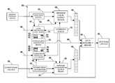
- FIG. 2illustrates a simplified block diagram of a computer system 200 , in accordance with an embodiment of the invention.
- system 200includes one or more processors 202 , a link controller 206 , and one or more memory modules 208 - 211 .
- processors 202For ease of description, only a single processor 202 and link controller 206 are illustrated and discussed. However, multiple processors 202 and/or link controllers 206 could exist within a system. Similarly, although four memory modules 208 - 211 are illustrated, more or fewer memory modules also could exist within a system.
- each memory module 208 - 211is located on a separate substrate, such as an insertable printed circuit board.
- multiple memory modulescould be located on a single substrate, and/or portions of the memory modules could be distributed across multiple substrates.
- a memory modulein accordance with an embodiment of the invention, will be described in more detail later in conjunction with FIG. 3 .
- processor 202From time to time, processor 202 generates and sends requests for access to information stored within one or more of memory modules 208 - 211 . These “memory access requests” include requests to store data within memory modules 208 - 211 , as well as requests to retrieve data from memory modules 208 - 211 .
- processor 202one or more other requesters 204 could be present within the system 200 , in one embodiment.
- the system 200could include one or more other processors, interfaces, ports, adapters, or other entities which are capable of requesting data.
- Processor 202 and the one or more other requesters 204are referred to herein as “request originators.”
- Each access requestis initially processed by link controller 206 , which receives the access requests from the request originators 202 , 204 .
- link controller 206could be a North Bridge or some other type of processing element. Based on the content of the request, link controller 206 generates and sends one or more “memory access commands” to one or more of the memory modules 208 - 211 over a communications bus 220 , referred to herein as the “link bus.” If a memory access request asks for data to be retrieved (as opposed to stored), the memory modules 208 - 211 return the requested data to the link controller 206 over the link bus 220 , and the link controller 206 routes the requested data back to the request originator 202 , 204 .
- memory modules 208 - 211are operatively coupled together via the link bus 220 in a “tunneled” or “daisy-chained” configuration.
- link controller 206is interconnected over the link bus with a first memory module 208 .
- a first part 222 of the link bus 220interconnects link controller 206 and the first memory module 208 .
- the first memory module 208is interconnected over the link bus with a second memory module 209 .
- a second part 224 of the link bus 220interconnects first memory module 208 and a second memory module 209 , and so on.
- the link bus 220is a parallel bus.
- the link bus 220is 32-bits wide.
- the link bus 220could be wider or narrower than 32 bits, or it could be a serial bus.
- the terms “downstream” and “upstream”will be used throughout a remainder of this description.
- the bottom memory module 211exists at the furthest downstream end of the link bus 220
- the link controller 206exists at the furthest upstream end of the link bus 220 . Accordingly, data and information that a memory module receives from the direction of the last memory module 211 is considered to be received from a downstream direction. In contrast, data and information that a memory module receives from the direction of the link controller 206 is considered to be received from an upstream direction.
- memory module 211is considered to be downstream from memory module 210
- memory modules 210 and 211are considered to be downstream from memory module 209
- memory modules 209 - 211are considered to be downstream from memory module 208 .
- Each memory module 208 - 210(except for the lowest memory module 211 ) provides a tunneled connection to any downstream memory module.
- additional memory modulescould be added downstream from memory module 211 , or additional memory modules could be inserted at any other point in the tunnel (e.g., between or above one or more existing memory modules).
- each memory module 208 - 210passes each received, memory access command to its next downstream memory module, regardless of the command destination (e.g., the memory module to which the command is addressed). In another embodiment, each memory module 208 - 210 passes a received, memory access command in the downstream direction only if it is not the destination of the command.
- downstream dataAny type of information received from a downstream direction is referred to herein as “downstream data,” which could include data retrieved from memory, headers and other protocol information, and any other type of information received from a downstream memory module.
- upstream datais used herein to mean any type of information received from upstream direction, and could include memory access commands, data to be stored, headers and other protocol information.
- datais not meant to be limited only to actual data that is stored or retrieved. This term is also meant to include headers, other protocol information, commands, and other types of information.
- FIG. 3illustrates a simplified block diagram of a memory module 300 , in accordance with an embodiment of the invention.
- each memory module 300includes a hub 302 and one or more memory storage units 304 .
- a hubin accordance with an embodiment of the invention, will be described in more detail later in conjunction with FIG. 4 .
- hub 302 and memory storage units 304are co-located on a single substrate (e.g., a printed circuit board), which is removably connectable to the communications bus.
- hub 302 and one or more of the memory storage units 304could be located on separate substrates, and/or the substrates could be permanently connectable to the bus. Either way, each hub 302 has a set of memory storage units 304 associated with it, and which it may access exclusively. Accordingly, each memory module 300 can be considered a “data source.”
- Memory storage units 304could be connected to hub 302 through a common link (as shown), through point-to-point connections, through a daisy chain link, or in some other way.
- each memory storage unit 304is a distinct memory component, such as a dynamic random access memory (DRAM) device, for example.
- DRAMdynamic random access memory
- memory storage units 304could include other types of memory devices (e.g., read only memory (e.g., ROM, PROM, EEPROM, etc.), flash memory or other memory types). Although four memory storage units 304 are illustrated in FIG. 3 , more or fewer units 304 could be included on any memory module 300 .
- Hub 302includes one or more application-specific integrated circuits (ASICs), in one embodiment. In another embodiment, hub 302 includes one or more general-purpose or specific-purpose processors. Hub 302 communicates over the upstream link bus 310 to upstream memory modules 208 ( FIG. 2 ) or to link controller 206 . In addition, if any downstream memory modules exist, hub 302 communicates over the downstream link bus 312 to downstream memory modules. Accordingly, hub 302 receives data from downstream memory modules on a first part of the bus (i.e., the downstream link bus 312 ), and sends data toward the link controller 206 on a second part of the bus (i.e., the upstream link bus 310 ).
- ASICsapplication-specific integrated circuits
- hub 302includes one or more general-purpose or specific-purpose processors. Hub 302 communicates over the upstream link bus 310 to upstream memory modules 208 ( FIG. 2 ) or to link controller 206 . In addition, if any downstream memory modules exist, hub 302 communicates over
- hub 302when hub 302 receives a memory access command on the upstream link bus 310 , hub 302 retransmits the command on the downstream link bus 312 , and stores information regarding the command in a command queue (see element 412 , FIG. 4 , described later). Hub 302 also determines whether it is the destination of the command. If so, hub 302 makes whatever accesses are necessary to the memory storage units 304 associated with the memory module 300 , and sends the requested data on the upstream link bus 310 . In addition, hub 302 receives data on the downstream link bus 312 from downstream memory modules (not shown), and hub 302 retransmits that data on the upstream link bus 310 .
- hub 302receives data from at least two sources: a) data from the memory storage units 304 ; and b) data from downstream memory modules.
- Data retrieved by hub 302 from the memory storage units 304 associated with the hub 302are referred to herein as “local data.”
- data received by hub 302 from one or more downstream memory modules on the downstream link bus 312are referred to herein as “downstream data.”
- local data and downstream datamight be construed to mean that only two data sources exist within the system, the terms are not meant to be so limiting. Data could originate from one or multiple other sources (e.g., one or multiple downstream memory modules or other sources).
- hub 302receives both the local data and the downstream data, and to provide both to the upstream link bus 310 .
- hub 302receives the local data and downstream data, and sends them on the upstream link bus 310 in a manner that efficiently uses the resources available on the upstream link bus 310 .
- the datais merged and sent without causing significant data “gaps” on the bus, where a “gap” includes one or more bits sent over the link bus without valid data, even though valid downstream or local data is available to be returned. The way that this is accomplished is described in detail, in conjunction with the embodiments illustrated in FIGS. 4-8 .
- FIG. 4illustrates a simplified, functional block diagram of a hub 400 , in accordance with an embodiment of the invention.
- hub 400includes various functional elements, which are illustrated as distinct blocks in FIG. 4 , for the purposes of illustration.
- the actual logic elements and hardware associated with each functional elementcould be resident in a single ASIC, or could be resident in multiple ASICs and/or other discrete devices.
- various aspects of the functional elements illustrated in FIG. 4could be implemented in hardware, software or both.
- hub 400receives local data and downstream data, determines how the data from the two sources will be merged together, and provides the merged data to the upstream link bus 452 .
- the functional components of hub 400are briefly described in the next paragraph, in accordance with one particular embodiment. Other embodiments and additional details are included in the description that follows.
- Hub 400includes a local data buffer 410 and a downstream data buffer 420 , which are used as means to receive and store local data and downstream data, respectively, if necessary.
- Hub 400also includes local arbitration logic means 414 , downstream arbitration logic means 422 , and inter-source arbitration means 416 , which operate cooperatively to determine how the local data and downstream data will be sent on the upstream link bus 452 .
- Hub 400also includes means for arranging local output 430 , means for arranging downstream output 432 , and data assembly means 450 , which function to arrange the local data and the downstream data into a data block structure, in accordance with the determinations made by the arbitration means 414 , 416 , 422 .
- the data block structureis represented by buffers 440 , 442 .
- the data organized into the data block structureis sent on the upstream link bus 452 in a contiguous manner.
- hub 400includes command queue 412 , into which the hub stores information relating to received memory access commands.
- the data block structure(also referred to herein as a “data block”) includes a fixed number of configurable bits, in one embodiment.
- a data blockincludes 256 bits. In alternate embodiments, more or fewer bits could be present within a data block.
- the bits of the data block structureare appropriately configured (e.g., by filling them with a “1” or “0”) with data, and the data is clocked out onto the bus during a data block transmission period (i.e., one or more link bus clock cycles, described later).
- the data blockis divided into an integer number of contiguous “lanes,” where each lane includes a set of configurable bits.
- the data blockincludes a set of 8 lanes.
- the number of lanes within the data block structureis fixed, in one embodiment, and each lane includes the same number of bits. In other embodiments, the number of lanes could vary, and/or the number of bits per lane could differ from lane to lane.
- the lane structureis represented in FIG. 4 by buffers 440 , 442 .
- Each buffer 440 , 442represents a data block with 8 lanes, labeled “0” through “7”. In practice, buffers 440 , 442 could be separate buffers, or they could be the same buffer. Buffers 440 , 442 are represented separately in FIG. 4 for ease of description.
- each lanewould include 32 bits. Accordingly, lane 0 could be designated as bits 0 - 31 , lane 1 could be designated as bits 32 - 63 , lane 2 could be designated as bits 64 - 95 , and so on, with lane 7 being designated as bits 224 - 255 . In alternate embodiments, more or fewer lanes could be present within a data block. For example, a data block could include as few as two lanes. In other alternate embodiments, lane 0 could include the most significant bits and lane 7 could include the least significant bits, or vice versa, or the bits allocated to each lane could be allocated in a non-sequential manner.
- the lane structure of the various embodimentsenables the hub 400 to efficiently send data over the upstream link bus 452 , when data is available from both a local and downstream source.
- the hub 400performs several basic processes. First, the hub determines when data from first and second sources (e.g., the local and downstream sources, or vice versa) are received and available. Second, an arbitration process is performed to determine which data will be granted access to the upstream link bus during any particular data block transmission period. Third, a lane filling process is performed to identify which lanes will be utilized by which data during a particular data block transmission period.
- the lane filling processinvolves allocating one or more first contiguous lanes within a first section of a data block to at least some of the first source data, and allocating one or more second contiguous lanes within a second section of the data block to at least some of the second source data, where the second section begins at a next lane, which is contiguous with the first section. Finally, the portions of the first source data and the second source data are sent over the communications bus during the data block transmission period.
- downstream datais received from the downstream link bus 454 .
- the downstream datais either placed into a downstream data buffer 420 , or is routed to a downstream flythrough path 472 .
- local datais received from memory storage unit(s) 402 (e.g., units 304 , FIG. 3 ).
- the local datais either placed into a local data buffer 410 , or is routed to a local flythrough path 470 .
- the downstream flythrough path 472 and the local flythrough path 470are used, in one embodiment, when no downstream or local data remain unsent in the downstream data buffer 420 or local data buffer 410 , and when data from only one source is vying for the upstream bus 452 . In these situations, the data from either source is simply granted the bus, in order to expedite the return of the data to the requester. In other embodiments, either or both flythrough paths 470 , 472 could be excluded from the system, and the local and downstream data could be buffered regardless of the state of buffers 410 , 420 .
- the remainder of the descriptionassumes that multiple sources are vying for the bus, and that local data and downstream data are being temporarily stored in the local data buffer 410 and/or the downstream data buffer 420 , respectively, rather than being routed through either flythrough path 470 , 472 . Accordingly, data from multiple sources are assumed to be available, in much of the description that follows, and the multiple sources are vying for access to the upstream link bus 452 .
- downstream data strobe signal 408is sent to the downstream arbitration logic means 422 . Assuming that the downstream data is being placed into the downstream data buffer 420 , a downstream buffer status signal 467 indicates that the downstream data buffer is not empty. When the buffer is not empty, the downstream flythrough path 472 is not used.
- Downstream arbitration logic means 422includes means for generating a bus access request. When the data strobe 408 and buffer status signal 467 indicate that downstream data is available to be sent over the upstream link bus 452 , the downstream arbitration logic means 422 sends a downstream request signal 461 to the inter-source arbitration means 416 . The downstream request asks the inter-source arbitration means 416 to allow the downstream arbitration logic means 422 to provide its downstream data on the upstream link bus 452 .
- a local data strobe signal 404is sent to the local arbitration logic means 414 . Assuming that the local data is being placed into the local data buffer 410 , a local buffer status signal 477 indicates that the local data buffer is not empty. When the buffer is not empty, the local flythrough path 470 is not used.
- Local arbitration logic means 414includes means for generating a bus access request.
- the local arbitration logic means 414sends a local request signal 471 to the inter-source arbitration means 416 . Similar to the downstream side previously discussed, the local request asks the inter-source arbitration means 416 to allow the local arbitration logic means 414 to provide its local data on the upstream link bus 452 .
- inter-source arbitration means 416receives requests 471 , 461 to access the bus from both local arbitration logic means 414 and downstream arbitration logic means 422 .
- Inter-source arbitration means 416includes a means for making a determination of how the local and downstream data will be sent over the bus. Accordingly, when multiple requests are pending, means 416 performs an arbitration process, and grants access to the local or downstream data.
- Neither the local or downstream arbitration logic means 414 , 422send their data until they have been granted access to the bus.
- the inter-source arbitration means 416decides to switch a grant from one source to another, the inter-source arbitration means 416 determines and indicates where the next source should start its data, within the lane structure. Inter-source arbitration means 416 uses various information from the downstream and local arbitration logic means 422 , 414 to make this determination.
- a source that is granted access to the buspredicts where a “breakpoint” in its data will occur, and informs the inter-source arbitration means 416 of the predicted location of the breakpoint.
- the inter-source arbitration means 416uses that predicted location to determine where, within the lane structure, the next granted source may begin to insert its data.
- FIG. 5illustrates an example of a timing diagram, in accordance with an embodiment of the invention. Initially, only the internal clock signal 502 and the lane data signals 508 - 515 will be discussed. The other signals shown in FIG. 5 will be discussed later.
- Signal 502represents an internal clock signal.
- the internal clock signalis used to define a “processing period” within which each data block is assembled.
- a processing periodrefers to a period of time within which a single data block is assembled.
- FIG. 5illustrates a processing period that is one internal clock cycle long, a processing period may be longer or shorter than one internal clock cycle.
- the data blockincludes 8 lanes, and valid data is available in those lanes as indicated by lane data signals 508 - 515 .
- datais inserted into the lanes 508 - 515 of the data block structure. Once assembled, that data is made available to the bus.
- a next processing period 542different data is inserted into the lanes 508 - 515 of the data block structure, and subsequently made available to the bus.
- the relationship between the various edges of the internal clock (i.e., the rising and falling edges) and the data and other signalsis illustrated in one particular way in FIG. 5 , this relationship could be different, in other embodiments.
- the clock signalcould be inverted with respect to the other signals.
- Other modificationscould be contemplated as well.
- a particular memory access requestis considered a “transaction,” and a transaction identifier is associated with the request in order to identify data that is returned.
- a transactioncan be virtually any length. For example, a transaction could be as short as a single bit, or a transaction could be millions of bits long.
- the data associated with a transactionis returned as a set of “data fragments,” with each fragment including a number of bits that corresponds to the width of a lane. For example, if a transaction includes 256 bits, and each lane is 32 bits wide, then the transaction could be divided into 8 data fragments.
- a headermay be sent along with the data for a transaction, in order to identify the data.
- a headercould be of any length. In the embodiment described below, a header consumes no more than one lane. In other embodiments, a header could consume more than one lane, or a protocol could be used for which a header is not returned for each transaction.
- the first data being transferredincludes a header 550 , located in lane “0” 508 , and a first portion of local data consisting of seven fragments of local data, which are shown in lanes “1-7” 509 - 515 .
- the symbols included in each data envelopeare represented as follows: “L” indicates local data; “R” indicates downstream (or remote) data; “T*” indicates the transaction number; and “D*” indicates the data fragment number for the transaction.
- the identifier “L_T 0 _D 0 ” shown in lane “1” 509indicates that the data within lane “1” during processing period 540 corresponds to the first fragment (D 0 ) of local data (L), for the local transaction identified by “0” (T 0 ).
- the identifier “R_T 0 _D 7 ” shown in lane “1” 509 during processing period 544indicates that the data corresponds to the eighth fragment (D 7 ) of downstream data (R), for the downstream transaction identified by “0” (T 0 ).
- the inter-source arbitration means( 416 , FIG. 4 ) previously granted access to the bus to the local source.
- the local sourcehad eight data fragments to send during the first grant. Because the header 550 consumed lane “0” 508 during the first processing period 540 , only seven of the eight data fragments could be assembled during that first processing period 540 .
- the remainder portion of the local source data, consisting of the eighth fragment designated “L_T 0 _D 7 ,”is shown to be placed in lane “0” during the second processing period 542 .
- the end of the eighth fragment “L_T 0 _D 7 ”represents a “breakpoint” in the local source data. This breakpoint coincides with the beginning of lane “1” 509 of the second processing period 542 .
- data from the local or downstream sourcecan be used to fill the remaining lanes “1-7” for the second processing period 542 .
- the inter-source arbitration means( 416 , FIG. 4 ), granted access next to the downstream source (R).
- the downstream sourcehas a header, and 16 data fragments (D 0 through D 15 ) to send during its first transaction (T 0 ). Because the breakpoint occurs at the beginning of lane “1” 509 of the second processing period 542 , the header can be placed there.
- the 16 data fragmentsfollow, as indicated by the indicators “R_T 0 _D 0 ,” in lane “2” 510 of the second processing period 542 , through “R_T 0 _D 15 ,” in lane “1” 509 of the fourth processing period 546 .
- 6 of the 16 data fragments(R_T 0 _D 0 through R_T 0 _D 5 ) are placed in lanes 2-7 of the second processing period 542 .
- a remainder portion of data from a first sourceis placed in a first section of the data block structure
- a portion of data from a second sourceis placed in a second section of the data block structure.
- the third processing period 544is consumed entirely by the R_T 0 transaction, and no breakpoint occurs during that period.
- the breakpoint of the downstream transactiondoes not occur until the beginning of lane “2” 510 of the fourth processing period 546 .
- a header and the first 5 of 10 local data fragments for a second local transaction, designated “T 1 ,”are assembled during the fourth and fifth processing periods 546 , 548 .
- data from multiple sourcescan be placed in the lanes to be sent out during a particular data block transmission period. This is particularly illustrated during processing periods 542 and 546 .
- data from a first sourcee.g., local data or downstream data
- data from a second sourcee.g., downstream data or local data
- both first source data and second source datacan be sent on the upstream link bus during a single data block transmission period.
- first source datais placed in a first section of a data block
- second source datais placed in a second section of the data block, where the second section begins at a next lane, which is contiguous with the first section.
- local data associated with a first local transaction(“L_T 0 ”) is indicated as being available by the state of the local data signal 504 .
- downstream data associated with a first downstream transaction(“R_T 0 ”) is indicated as being available by the state of the downstream data signal 506 .
- the local data signal 504corresponds to the data stored in local data buffer 410
- the downstream data signal 506corresponds to the data stored in downstream data buffer 420 .
- the local arbitration logic means 414sends a bus access request 471 to the inter-source arbitration means 416 .
- the downstream arbitration logic means 422also sends a bus access request 461 to the inter-source arbitration means 416 .
- Inter-source arbitration means 416uses various criteria to determine who will be granted the bus during any given processing period. When inter-source arbitration means 416 decides to grant the bus to a particular source, it sends a bus grant signal to that source. For example, as FIG. 5 indicates, the local data 504 (L_T 0 ) is first granted the bus. Accordingly, inter-source arbitration means 416 sends a bus grant signal 474 to local arbitration logic means 414 . In one embodiment, the bus grant signal 474 is sent during the processing period in which the data will actually be placed in the data block (e.g., processing period 540 ). In other embodiments, the signal 474 could be sent during a previous processing period.
- inter-source arbitration means 416sends a position indicator, described further below, that enables local arbitration logic means 414 to know in which lane the header or data should first be placed. In one embodiment, inter-source arbitration means 416 sends this indication in the form of a “next lane in” signal 475 to local arbitration logic means 414 .
- the “next lane in” for the first processing period 540is lane “0” 508 . Accordingly, lane “0” is the lane into which the local arbitration logic means 414 causes the header for its transaction data to be placed. Local arbitration logic means 414 then arranges its data so that the remaining lanes of the first processing period 540 will be filled with data fragments for its first transaction.
- arrange local output means 430receives a signal 476 from local arbitration logic means 414 , which indicates the next lane in. Arrange local output means 430 then retrieves the header, if one is to be assembled that processing period. In one embodiment, information to be included in the header is retrieved from the command queue 412 . In addition, means 430 retrieves the data, from the local data buffer 410 . Arrange local output means 430 arranges the header and/or data into a local pre-transmit data block 440 , which has the data block/lane structure.
- local output means 430would place the header in lane “0” of the local pre-transmit data block 440 , and would place the first seven data fragments (L_T 0 _D 0 through L_T 0 _D 6 ) in lanes “1” through “7.”
- means 414predicts the breakpoint of its data. In other words, it determines at which processing period, and in which lane, its data for the transaction will be completed. In one embodiment, this prediction is based on knowledge, by the local arbitration logic means 414 , of the transaction size, which was previously stored in the command queue 412 . In one embodiment, local arbitration logic means 414 predicts the breakpoint as the end of the entire transaction. In another embodiment, return of the data for a transaction could be performed in multiple parts (e.g., if the transaction exceeds a certain size), and the breakpoint could occur somewhere before the end of the data.
- the local arbitration logic means 414if it predicts that a breakpoint will occur within the next upcoming processing period, then it makes an indication that the breakpoint will occur by sending a local breakpoint indicator signal 472 to the inter-source arbitration means. In addition, means 414 makes an indication of the location of the end of the data, within the data block structure. In one embodiment, this is done by sending an indicator 473 of where, in the lane structure, the breakpoint will occur. These signals correspond to signals 526 and 524 , in FIG. 5 , respectively.
- the local data arbitration logic means 414knows that its transaction size includes 8 data fragments (D 0 -D 7 ), and thus it determines that it will only need to fill lane “0” 508 of the second processing period 542 , in order to complete the transaction. Accordingly, local data arbitration logic means 414 would determine that a breakpoint would be occurring in the next processing period 542 .
- local data arbitration logic means 414indicates to the inter-source arbitration means 416 that a breakpoint will be occurring. In the illustrated embodiment, this indication is made by setting signal 472 , 526 to a high state. In alternate embodiments, a low setting could be used, or some other type of indication could be made. Because the local breakpoint signal 472 , 526 is a binary indication (i.e., either there is an upcoming breakpoint or not), the signal can be represented with a single bit or wire.
- next local lane signal 473( FIG. 4 ), 524 ( FIG. 5 )
- local data arbitration logic means 414indicates to the inter-source arbitration means 416 where the next breakpoint will occur within the lane structure.
- this indicationcomes in the form of an identification of which lane will first be available, in the next processing period 542 .
- the next local lane signal 473 , 524could carry a “1,” indicating that lane “1” 509 will be available to another source, if the other source is granted bus access.
- next local lane signal 473 , 524could indicate which lane would carry the last fragment of data for the current transaction (e.g., “L_T 0 _D 7 ,” in the current example). In such an embodiment, the next local lane signal 473 , 524 would carry a “0,” indicating that lane “0” 508 will carry the last fragment.
- next local lane signal 473 , 524indicates the identity of a lane
- the number of bits that could be used for the signal 473 , 524is sufficient to make such an indication. In an embodiment that uses 8 lanes, 3 bits of information or wires could be used for the signal 473 , 524 .
- inter-source arbitration means 416could receive other types of information that enable it to determine whether a breakpoint will occur in the next processing period, and where that breakpoint will occur. Alternatively, inter-source arbitration means 416 could make either or both of these determinations itself. In still other embodiments, an arbitration means, 414 , 416 or 422 , could determine and indicate where a breakpoint will occur, even if the breakpoint will occur during a processing period that occurs after the next processing period. Numerous alternate embodiments could be contemplated, and those embodiments are intended to fall within the scope of the present invention.
- inter-source arbitration means 416may decide to grant the bus to the same source (i.e., the local source, in the current example) or to another source (i.e., the downstream source, in the current example) during the next period 542 .
- inter-source arbitration unit 416decides to grant the bus to the downstream data 506 (R_T 0 ), which also had a pending request from the first processing period 540 .
- inter-source arbitration unit 416sends a bus grant signal 464 to downstream arbitration logic means 422 .
- the signal 464is sent during the second processing period 542 .
- the signal 464could be send earlier (e.g., during the first processing period 540 ).
- inter-source arbitration means 416sends a position indicator, which enables downstream arbitration logic means 422 to know in which lane its header or data should first be placed. In one embodiment, inter-source arbitration means 416 sends this indication in the form of the next lane in signal 465 to downstream arbitration logic means 422 .
- the next lane in signal 465could include a “lane identifier,” which is an integer number identifying the lane. For example, in the example where 8 lanes exist within the data block structure, the lane identifiers could be the integer numbers from 0 to 7. In other embodiments, a bit number within the data structure (e.g., a number from 0 to 255 for a 256 bit data structure) or some other indication of the location of the breakpoint could be sent.
- the next lane in signal 465corresponds to the next local lane signal 524 sent by the previously granted source (e.g., the local source, in this case), during the previous processing period 540 .
- the next local lane signal 524 sent by the local arbitration logic means 414 during the previous processing periodwas a “1”, meaning that lane “1” 509 is the first lane available after the breakpoint of the local data.
- next lane in signal 465could be a value that is based on the value of the next local lane signal 524 , although it may not be exactly the same.
- the next local lane signal 524may indicate the last lane that the local data will consume, and the next lane in signal 465 could indicate the first lane that the downstream data should first occupy.
- the next local lane signals and next lane in signalscould be indicated in a manner other than with a lane identifier. For example, either or both could indicate a bit position, within the data block, or could be indicated in some other manner.
- the “next lane in” for the second processing period 542is lane “1” 509 , as was indicated during processing period 540 . Accordingly, lane “1” is the lane into which the downstream arbitration logic means 422 causes the header for its transaction data to be placed. Downstream arbitration logic means 422 then arranges its data so that the remaining lanes for the second processing period 542 will be filled with data fragments for its first transaction.
- downstream arbitration logic means 422predicts the breakpoint of its data. In one embodiment, this prediction is based on knowledge, by the downstream arbitration logic means 422 , of the transaction size, which was previously stored in the command queue 412 .
- the transaction sizeis 16 data fragments. Accordingly, the breakpoint will not occur during the third processing period 544 (i.e., the next processing period). Instead, the predicted breakpoint occurs in the fourth processing period 546 . Further, the downstream data arbitration logic means 422 knows that its transaction size includes 16 data fragments (D 0 -D 15 ), and thus it determines that it will fill lane “0” and “1” of the fourth processing period 546 , in order to complete the transaction.
- the downstream arbitration logic means 422causes the remaining contiguous lanes to be filled with its header and data fragments. However, because a breakpoint will not be occurring during the next processing period 544 , it does not indicate, during processing period 542 , via the downstream breakpoint signal 462 , 530 , that a breakpoint is upcoming. Instead, as is discussed below, this indication is made during processing period 544 .
- downstream arbitration logic means 422causes the entire data block to be filled with its transaction data (D 6 -D 13 ). Now, because a breakpoint will be occurring during the next processing period 546 , downstream arbitration logic means 422 indicates, via the downstream breakpoint signal 462 , 530 , that a breakpoint is upcoming. In addition, downstream arbitration logic means 422 indicates, via the next downstream lane signal 463 , 528 , the location of the breakpoint. As the next downstream lane signal 528 of the example of FIG. 5 indicates, the breakpoint will occur in lane “2” 510 during the fourth processing period 546 .
- inter-source arbitration means 416may decide to grant the bus to the same source (i.e., the downstream source, in the current example) or to another source (i.e., the local source, in the current example) during the next period 546 .
- inter-source arbitration unit 416decides to grant the bus to the local data 506 (R_T 1 ), which had a pending request from the second processing period 542 . The process then continues to repeat itself.
- local arbitration logic means 414 and downstream arbitration logic means 422arrange their data so that the lanes of the data block, for any given processing period, are correctly filled with either local or downstream data. In one embodiment, this is done as follows, using the example of the second processing period 542 ( FIG. 5 ).
- Arrange downstream output means 432receives a signal 466 from local arbitration logic means 414 , which indicates the next lane in. Arrange downstream output means 432 then retrieves the header, if one is to be assembled that processing period. In one embodiment, information to be included in the header is retrieved from the command queue 412 . In addition, means 432 retrieves the data, from the downstream data buffer 420 . Arrange downstream output means 432 arranges the header and/or data into a downstream pre-transmit data block 442 , which has the data block/lane structure.
- downstream output means 432would place the header in lane “1” of the downstream pre-transmit data block 442 , and would place the first six data fragments (R_T 0 _D 0 through R_T 0 _D 5 ) in lanes “2” through “7.”
- lane “0” of the data blockis allocated to the remainder of the data from the local source. Accordingly, arrange local output means 430 would place that remainder data in the local pre-transmit data block 440 . Specifically, it would place the last data fragment (L_T 0 _D 7 ) from the transaction into lane “0” of the local pre-transmit data block 440 .
- inter-source arbitration means 416sends a “local/downstream select” signal 460 to data assembly means 450 .
- Data assembly means 450includes a means for assembling the data and sending the data over the upstream link bus 452 during a data block transmission period.
- the local/downstream select signal 460is a signal having a number of bits that corresponds to the number of lanes in the data block structure.
- the local/downstream select signal 460is an eight bit signal, where each bit corresponds to a lane. If a bit is in a first state (e.g., 0) it may indicate to the data assembly means 450 that it should retrieve data from the corresponding lane of the local pre-transmit data block 440 , and if the bit is in a second state (e.g., 1), it may indicate that the data should be retrieved from the corresponding lane of the downstream pre-transmit data block 442 , or vice versa.
- a first statee.g., 0
- a second statee.g., 1
- the local/downstream select signal 460corresponds to lane “0,” and the least significant bit of the signal corresponds to lane “7.” Assume also that a value of “0” indicates the local source, and a value of “1” indicates the downstream source.
- the local/downstream select signal 460would have a value of “0 1 1 1 1 1 1”.
- the signal 460would have a value of “1 1 0 0 0 0 0 0 0 0”.
- which bit corresponds to which particular lanecould be different.
- a value of “1”could indicate the local source and “0” could indicate the local source.
- the data assembly means 450could determine which source to use for which lane using information that is differently formatted.
- a separate local pre-transmit data block 440 and downstream pre-transmit data block 442might not be used. Instead, data from the local and downstream source could be placed directly into a single pre-transmit data block (not illustrated). In this embodiment, it may not be necessary to inform data assembly means 450 of the configuration of the lanes (i.e., which source is granted which lane). Instead, data assembly means 450 could simply provide the data in the single pre-transmit data block to the upstream link bus 452 .
- the internal clock signal 502operates at a lower frequency than the link bus clock, and the link bus clock frequency is approximately an integer multiple of the internal clock signal 502 frequency.
- the internal clock signal 502could operate at a frequency in the Megahertz (MHz) range, while the link bus clock could operate at a frequency in the Gigahertz (GHz) range.
- the internal clock and/or the link bus clockcould operate at higher or lower data frequencies, as well.
- the clockscould operate at approximately the same frequency, in other embodiments.
- Each link bus clock cycle, data provided by data assembly means 450can be sent over the upstream link bus 452 .
- one data blockis sent out over the upstream link bus 452 during a single “data block transmission period,” where a data block transmission period could be one or multiple link bus clock cycles long.
- each data blockincludes 64 bits of data. If the link bus is 32 bits wide, then two link bus clock cycles could be used to send one data block.
- the frequency of the link bus clockcould be two times the frequency of the internal clock, assuming that a processing period (e.g., period 540 ) is one internal clock cycle long, which may not be the case. For example, if the internal clock is operating at 400 MHz, the link bus clock could operate at about 800 MHz.
- the link bus clockcould be 16 times the frequency of the internal clock. For example, if the internal clock is operating at 400 MHz, the link bus clock could operate at about 6.4 GHz.
- FIGS. 6 and 7are now described, in order to provide further understanding of the various embodiments.
- FIG. 6illustrates a flowchart of a method for requesting access to the bus, in accordance with an embodiment of the invention.
- all or portions of the methodcould be performed by local arbitration logic means 414 ( FIG. 4 ) and/or downstream arbitration logic means 422 ( FIG. 4 ).
- other functional elementscould perform all or portions of the method.
- first source and second sourceare used to describe an entity requesting access to the upstream bus. These terms are not meant to specifically identify the local or downstream arbitration logic means 414 , 422 .
- the methodbegins, in block 602 , by determining whether data from a first source is available for transmission over the upstream link bus. In one embodiment, this determination can be made from the state of a data strobe signal (e.g., strobe 404 , 408 , FIG. 4 ). In another embodiment, the determination could be made from a buffer empty/not empty signal (e.g., signal 477 , 467 , FIG. 4 ). The determination could be made in other ways, as well, in other embodiments. If no first source data is available, the method waits.
- a data strobe signale.g., strobe 404 , 408 , FIG. 4
- the determinationcould be made from a buffer empty/not empty signal (e.g., signal 477 , 467 , FIG. 4 ). The determination could be made in other ways, as well, in other embodiments. If no first source data is available, the method waits.
- first source datais available, then the first source sends a bus access request, in block 604 .
- the requestis sent to the inter-source arbitration means 416 ( FIG. 4 ).
- the inter-source arbitration means 416could receive requests from other sources as well, during a particular internal processing period.
- the inter-source arbitration means 416is responsible for arbitrating the incoming bus access requests, and granting access.
- the first sourcewaits for a grant indication from the inter-source arbitration means 416 , in block 606 .
- the first sourcelooks for a next lane available indicator from the inter-source arbitration means 416 .
- the next lane available indicatortells the first source where it should begin to place a header and/or data, within the data block being constructed for transmission.
- the first sourcethen arranges its data within the data block, accordingly.
- datais arranged within one or more pre-transmission data blocks (e.g., blocks 440 , 442 , FIG. 4 ).
- pre-transmission data blockse.g., blocks 440 , 442 , FIG. 4 .
- only one sourceplaces data within the data block, while during other processing periods, at least two sources place data within the data block.
- the first sourceWhen it is determined that the first source's transaction will be completed during a next processing period, then in block 612 , the first source indicates, to the inter-source arbitration unit 416 ( FIG. 4 ), that a breakpoint will occur. In addition, the first source sends an indication of where the breakpoint will occur. For example, the first source could send the identity of the next lane available after the end of the transaction.
- the first sourcethen arranges any remaining data, in block 614 , within one or more first contiguous lanes within a first section of the next data block. If no data remains (e.g., if the breakpoint occurred after the last lane of the previous period), then the first source does not place any data within the next data block. The method then repeats.
- inter-source arbitration unit 416decides to grant the bus next to a second source, then data from the second source will be placed within one or more second contiguous lanes within a second section of the data block, where the second section begins at a next lane, which is contiguous with the first section.
- the first source data and the second source dataare sent over the bus during a data block transmission period (i.e., one or more link bus clock cycles).
- FIG. 7illustrates a flowchart of a method for granting access to the bus, in accordance with an embodiment of the invention.
- all or portions of the methodcould be performed by inter-source arbitration logic means 416 ( FIG. 4 ).
- other functional elementscould perform all or portions of the method.
- the methodbegins, in block 702 , when a bus access request is received from a first source.
- a bus access requestcould be made by the local arbitration logic means 414 ( FIG. 4 ) or the downstream arbitration logic means 422 ( FIG. 4 ).
- the inter-source arbitration logic means 416could have from zero to many bus access requests pending, meaning that the requesters had not yet been granted access to the bus.
- a breakpointe.g., an identity of the next lane available
- the inter-source arbitration means 416may then control the assembly and transmission of the data within the data block to be sent. In one embodiment, this is achieved by sending a local/downstream select signal 460 ( FIG. 4 ), to the functional element (e.g., data assembly means 450 , FIG. 4 ) that is responsible for multiplexing and sending the data over the upstream link bus. The method then ends.
- a breakpoint signale.g., signals 472 , 462 , FIG. 4
- the identity of the location of the breakpointis determined, in block 708 .
- the location of the breakpointis determined by observing a “next lane out” signal (e.g., signals 473 , 463 , FIG. 4 ) provided by the source that is using the bus.
- any pending requestsare arbitrated, to determine who will be granted access to use the bus next.
- the arbitration processcan use various criteria in determining who will gain access to the bus.
- the inter-source arbitration means 416may indicate, to another source that has requested access to the bus, that it is granted access to the bus, in block 716 .
- the inter-source arbitration means 416may indicate where the breakpoint will occur (e.g., an identity of the next lane available). Block 718 is then performed, and the method ends.
- the hub architectureis described as being implemented primarily in hardware, in embodiments described above.
- one or more elements of the hub architecturecould be implemented in firmware or software, as a series of instructions which, when executed by a microprocessor or other computing device, perform the same function and produce the same result as the embodiments described above.
- a set of computer-executable instructions for performing the functions of the hubcould be stored on a computer-readable medium (e.g., a hard disk, optical or magnetic disk, ROM, RAM, or virtually any other computer-readable medium).
- FIG. 8illustrates an electronic system, in accordance with an embodiment of the invention.
- FIG. 8 and the following discussionare intended to provide a brief, general description of a suitable environment in which embodiments of the invention may be implemented.
- Those skilled in the artwill appreciate that the invention may be practiced with other computer system configurations, including hand-held devices, multi-processor systems, microprocessor-based or programmable consumer electronics, network personal computers, minicomputers, mainframe computers, database computers, and the like.
- the system shown in FIG. 8includes a general purpose computer 800 , which includes one or more processing units 810 , a North Bridge 812 , system memory 814 , and a system bus 820 , which interconnects various system components, and may be any of several types of bus structures.
- a general purpose computer 800which includes one or more processing units 810 , a North Bridge 812 , system memory 814 , and a system bus 820 , which interconnects various system components, and may be any of several types of bus structures.
- the North Bridge 812acts as an interface between the system bus 820 and the processing unit 810 and system memory 814 , in one embodiment. Accordingly, the North Bridge 812 operates as an input/output (I/O) controller and a memory controller. In one embodiment, the North Bridge 812 may contain a link controller, in lieu of a memory controller.
- the North Bridge 812communicates with the processing unit 810 over a processor bus 816 , and communicates with system memory 814 over a memory bus 818 .
- system memory 814is configured in accordance with an embodiment of the invention. Accordingly, system memory 814 includes one or more memory modules 824 (e.g., modules 208 , FIG. 2 ). Further, system memory 814 could include a link controller (e.g., controller 206 , FIG. 2 ), and/or read only memory (ROM) 825 , and/or random access memory (RAM) 826 , in various embodiments.
- a link controllere.g., controller 206 , FIG. 2
- ROMread only memory
- RAMrandom access memory
- the computer 800further can include a hard disk drive 827 for reading from and writing to a hard disk, not shown, a magnetic disk drive 828 for reading from or writing to a removable magnetic disk 829 , and an optical disk drive 830 for reading from or writing to a removable optical disk 831 , such as a CD ROM or other optical media.
- the hard disk drive 827 , magnetic disk drive 828 , and optical disk drive 830can be connected to the system bus 820 by a hard disk drive interface 832 , a magnetic disk drive interface 833 , and an optical drive interface 834 , respectively.
- a usermay enter requests and information into the computer 800 through input devices, such as a keyboard 840 , pointing device 842 or other input devices (not shown). These and other input devices may be connected to processing units 810 through a serial port interface 846 that is coupled to the system bus, or may be connected by other interfaces, such as a parallel port, game port or a universal serial bus (USB).
- a monitor 847 or other type of display devicealso may be connected to the system bus 820 via an interface, such as a video adapter 848 .
- the systemmay also include other peripheral output devices (not shown), such as speakers and printers.
- the computer 800may operate in a networked environment using logical connections to one or more remote computers, such as a remote computer 849 .
- Computer 800 and remote computer 849may be clients, servers, routers, network personal computers, peer devices or other common network nodes.
- the logical connections depicted in FIG. 8include a local area network (LAN) 851 and a wide area network (WAN) 852 .
- LANlocal area network
- WANwide area network
- the computer 800When used in a LAN networking environment, the computer 800 is connected to the local network 851 through a network interface or adapter 853 . When used in a WAN networking environment, the computer 800 typically includes a modem 854 or other means for establishing communications over the WAN 852 .
- the modem 854which may be internal or external, is connected to the system bus 820 via the serial port interface 846 . It will be appreciated that the network connections shown are exemplary and other means of establishing a communications link between the computers may be used.
Landscapes
- Engineering & Computer Science (AREA)
- Theoretical Computer Science (AREA)
- General Engineering & Computer Science (AREA)
- Physics & Mathematics (AREA)
- General Physics & Mathematics (AREA)
- Computer Hardware Design (AREA)
- Bus Control (AREA)
- Information Transfer Systems (AREA)
- Hardware Redundancy (AREA)
- Small-Scale Networks (AREA)
Abstract
Description
Claims (23)
Priority Applications (2)
| Application Number | Priority Date | Filing Date | Title |
|---|---|---|---|
| US13/692,269US8806152B2 (en) | 2003-10-17 | 2012-12-03 | Method and apparatus for sending data from multiple sources over a communications bus |
| US14/456,372US9652412B2 (en) | 2003-10-17 | 2014-08-11 | Method and apparatus for sending data from multiple sources over a communications bus |
Applications Claiming Priority (4)
| Application Number | Priority Date | Filing Date | Title |
|---|---|---|---|
| US10/688,461US7779212B2 (en) | 2003-10-17 | 2003-10-17 | Method and apparatus for sending data from multiple sources over a communications bus |
| US12/847,801US8095748B2 (en) | 2003-10-17 | 2010-07-30 | Method and apparatus for sending data from multiple sources over a communications bus |
| US13/345,379US8327089B2 (en) | 2003-10-17 | 2012-01-06 | Method and apparatus for sending data from multiple sources over a communications bus |
| US13/692,269US8806152B2 (en) | 2003-10-17 | 2012-12-03 | Method and apparatus for sending data from multiple sources over a communications bus |
Related Parent Applications (1)
| Application Number | Title | Priority Date | Filing Date |
|---|---|---|---|
| US13/345,379ContinuationUS8327089B2 (en) | 2003-10-17 | 2012-01-06 | Method and apparatus for sending data from multiple sources over a communications bus |
Related Child Applications (1)
| Application Number | Title | Priority Date | Filing Date |
|---|---|---|---|
| US14/456,372ContinuationUS9652412B2 (en) | 2003-10-17 | 2014-08-11 | Method and apparatus for sending data from multiple sources over a communications bus |
Publications (2)
| Publication Number | Publication Date |
|---|---|
| US20130097395A1 US20130097395A1 (en) | 2013-04-18 |
| US8806152B2true US8806152B2 (en) | 2014-08-12 |
Family
ID=34465593
Family Applications (5)
| Application Number | Title | Priority Date | Filing Date |
|---|---|---|---|
| US10/688,461Expired - LifetimeUS7779212B2 (en) | 2003-10-17 | 2003-10-17 | Method and apparatus for sending data from multiple sources over a communications bus |
| US12/847,801Expired - LifetimeUS8095748B2 (en) | 2003-10-17 | 2010-07-30 | Method and apparatus for sending data from multiple sources over a communications bus |
| US13/345,379Expired - Fee RelatedUS8327089B2 (en) | 2003-10-17 | 2012-01-06 | Method and apparatus for sending data from multiple sources over a communications bus |
| US13/692,269Expired - LifetimeUS8806152B2 (en) | 2003-10-17 | 2012-12-03 | Method and apparatus for sending data from multiple sources over a communications bus |
| US14/456,372Expired - Fee RelatedUS9652412B2 (en) | 2003-10-17 | 2014-08-11 | Method and apparatus for sending data from multiple sources over a communications bus |
Family Applications Before (3)
| Application Number | Title | Priority Date | Filing Date |
|---|---|---|---|
| US10/688,461Expired - LifetimeUS7779212B2 (en) | 2003-10-17 | 2003-10-17 | Method and apparatus for sending data from multiple sources over a communications bus |
| US12/847,801Expired - LifetimeUS8095748B2 (en) | 2003-10-17 | 2010-07-30 | Method and apparatus for sending data from multiple sources over a communications bus |
| US13/345,379Expired - Fee RelatedUS8327089B2 (en) | 2003-10-17 | 2012-01-06 | Method and apparatus for sending data from multiple sources over a communications bus |
Family Applications After (1)
| Application Number | Title | Priority Date | Filing Date |
|---|---|---|---|
| US14/456,372Expired - Fee RelatedUS9652412B2 (en) | 2003-10-17 | 2014-08-11 | Method and apparatus for sending data from multiple sources over a communications bus |
Country Status (8)
| Country | Link |
|---|---|
| US (5) | US7779212B2 (en) |
| EP (1) | EP1678621B1 (en) |
| JP (1) | JP4466653B2 (en) |
| KR (1) | KR100825238B1 (en) |
| CN (1) | CN100487685C (en) |
| AT (1) | ATE428984T1 (en) |
| DE (1) | DE602004020647D1 (en) |
| WO (1) | WO2005038660A2 (en) |
Cited By (1)
| Publication number | Priority date | Publication date | Assignee | Title |
|---|---|---|---|---|
| US9652412B2 (en) | 2003-10-17 | 2017-05-16 | Micron Technology, Inc. | Method and apparatus for sending data from multiple sources over a communications bus |
Families Citing this family (59)
| Publication number | Priority date | Publication date | Assignee | Title |
|---|---|---|---|---|
| US20040044508A1 (en)* | 2002-08-29 | 2004-03-04 | Hoffman Robert R. | Method for generating commands for testing hardware device models |
| US20050210185A1 (en)* | 2004-03-18 | 2005-09-22 | Kirsten Renick | System and method for organizing data transfers with memory hub memory modules |
| US7539800B2 (en) | 2004-07-30 | 2009-05-26 | International Business Machines Corporation | System, method and storage medium for providing segment level sparing |
| US7296129B2 (en) | 2004-07-30 | 2007-11-13 | International Business Machines Corporation | System, method and storage medium for providing a serialized memory interface with a bus repeater |
| US7441060B2 (en) | 2004-10-29 | 2008-10-21 | International Business Machines Corporation | System, method and storage medium for providing a service interface to a memory system |
| US7277988B2 (en) | 2004-10-29 | 2007-10-02 | International Business Machines Corporation | System, method and storage medium for providing data caching and data compression in a memory subsystem |
| US7305574B2 (en) | 2004-10-29 | 2007-12-04 | International Business Machines Corporation | System, method and storage medium for bus calibration in a memory subsystem |
| US7512762B2 (en) | 2004-10-29 | 2009-03-31 | International Business Machines Corporation | System, method and storage medium for a memory subsystem with positional read data latency |
| US7356737B2 (en) | 2004-10-29 | 2008-04-08 | International Business Machines Corporation | System, method and storage medium for testing a memory module |
| US7331010B2 (en) | 2004-10-29 | 2008-02-12 | International Business Machines Corporation | System, method and storage medium for providing fault detection and correction in a memory subsystem |
| US7778812B2 (en)* | 2005-01-07 | 2010-08-17 | Micron Technology, Inc. | Selecting data to verify in hardware device model simulation test generation |
| US20070016698A1 (en)* | 2005-06-22 | 2007-01-18 | Vogt Pete D | Memory channel response scheduling |
| US7652922B2 (en) | 2005-09-30 | 2010-01-26 | Mosaid Technologies Incorporated | Multiple independent serial link memory |
| KR101293365B1 (en) | 2005-09-30 | 2013-08-05 | 모사이드 테크놀로지스 인코퍼레이티드 | Memory with output control |
| US20070165457A1 (en)* | 2005-09-30 | 2007-07-19 | Jin-Ki Kim | Nonvolatile memory system |
| US20070076502A1 (en)* | 2005-09-30 | 2007-04-05 | Pyeon Hong B | Daisy chain cascading devices |
| US7478259B2 (en) | 2005-10-31 | 2009-01-13 | International Business Machines Corporation | System, method and storage medium for deriving clocks in a memory system |
| US7685392B2 (en)* | 2005-11-28 | 2010-03-23 | International Business Machines Corporation | Providing indeterminate read data latency in a memory system |
| US7471538B2 (en) | 2006-03-30 | 2008-12-30 | Micron Technology, Inc. | Memory module, system and method of making same |
| ATE488009T1 (en)* | 2006-03-31 | 2010-11-15 | Mosaid Technologies Inc | FLASH MEMORY SYSTEM CONTROL METHOD |
| US7636813B2 (en) | 2006-05-22 | 2009-12-22 | International Business Machines Corporation | Systems and methods for providing remote pre-fetch buffers |
| US7640386B2 (en) | 2006-05-24 | 2009-12-29 | International Business Machines Corporation | Systems and methods for providing memory modules with multiple hub devices |
| US7594055B2 (en) | 2006-05-24 | 2009-09-22 | International Business Machines Corporation | Systems and methods for providing distributed technology independent memory controllers |
| US7584336B2 (en) | 2006-06-08 | 2009-09-01 | International Business Machines Corporation | Systems and methods for providing data modification operations in memory subsystems |
| US7620763B2 (en)* | 2006-07-26 | 2009-11-17 | International Business Machines Corporation | Memory chip having an apportionable data bus |
| US7844769B2 (en)* | 2006-07-26 | 2010-11-30 | International Business Machines Corporation | Computer system having an apportionable data bus and daisy chained memory chips |
| US7493439B2 (en) | 2006-08-01 | 2009-02-17 | International Business Machines Corporation | Systems and methods for providing performance monitoring in a memory system |
| US7581073B2 (en) | 2006-08-09 | 2009-08-25 | International Business Machines Corporation | Systems and methods for providing distributed autonomous power management in a memory system |
| US7587559B2 (en) | 2006-08-10 | 2009-09-08 | International Business Machines Corporation | Systems and methods for memory module power management |
| US7539842B2 (en) | 2006-08-15 | 2009-05-26 | International Business Machines Corporation | Computer memory system for selecting memory buses according to physical memory organization information stored in virtual address translation tables |
| JP4476267B2 (en)* | 2006-10-06 | 2010-06-09 | 株式会社日立製作所 | Processor and data transfer unit |
| US7477522B2 (en) | 2006-10-23 | 2009-01-13 | International Business Machines Corporation | High density high reliability memory module with a fault tolerant address and command bus |
| US8745315B2 (en) | 2006-11-06 | 2014-06-03 | Rambus Inc. | Memory Systems and methods supporting volatile and wear-leveled nonvolatile physical memory |
| US7606988B2 (en) | 2007-01-29 | 2009-10-20 | International Business Machines Corporation | Systems and methods for providing a dynamic memory bank page policy |
| US7603526B2 (en) | 2007-01-29 | 2009-10-13 | International Business Machines Corporation | Systems and methods for providing dynamic memory pre-fetch |
| WO2008121559A1 (en) | 2007-03-30 | 2008-10-09 | Rambus Incorporated | System including hierarchical memory modules having different types of integrated circuit memory devices |
| CN100562021C (en)* | 2007-07-10 | 2009-11-18 | 北京易路联动技术有限公司 | A distributed and synchronizable multi-source data control method and device |
| US8601181B2 (en)* | 2007-11-26 | 2013-12-03 | Spansion Llc | System and method for read data buffering wherein an arbitration policy determines whether internal or external buffers are given preference |
| EP2192495A1 (en)* | 2008-11-11 | 2010-06-02 | Thomson Licensing | Method for processing data via triple-buffering |
| CN101930788A (en)* | 2009-06-24 | 2010-12-29 | 鸿富锦精密工业(深圳)有限公司 | Mobile storage device and storage device with mobile storage device |
| KR101796116B1 (en) | 2010-10-20 | 2017-11-10 | 삼성전자 주식회사 | Semiconductor device, memory module and memory system having the same and operating method thereof |
| US9104690B2 (en) | 2011-01-27 | 2015-08-11 | Micron Technology, Inc. | Transactional memory |
| JP5895378B2 (en)* | 2011-06-28 | 2016-03-30 | コニカミノルタ株式会社 | Data storage control device, data storage control method and program |
| EP3364304B1 (en) | 2011-09-30 | 2022-06-15 | INTEL Corporation | Memory channel that supports near memory and far memory access |
| JP5678257B2 (en)* | 2012-01-23 | 2015-02-25 | 株式会社日立製作所 | Memory module |
| KR20160069262A (en) | 2014-12-08 | 2016-06-16 | 에스케이하이닉스 주식회사 | Operation device module |
| US9514006B1 (en) | 2015-12-16 | 2016-12-06 | International Business Machines Corporation | Transaction tracking within a microprocessor |
| GB2553102B (en)* | 2016-08-19 | 2020-05-20 | Advanced Risc Mach Ltd | A memory unit and method of operation of a memory unit to handle operation requests |
| US10679722B2 (en) | 2016-08-26 | 2020-06-09 | Sandisk Technologies Llc | Storage system with several integrated components and method for use therewith |
| US11055241B2 (en)* | 2017-11-06 | 2021-07-06 | M31 Technology Corporation | Integrated circuit having lanes interchangeable between clock and data lanes in clock forward interface receiver |
| US11159153B2 (en) | 2018-03-29 | 2021-10-26 | Nvidia Corp. | Data bus inversion (DBI) on pulse amplitude modulation (PAM) and reducing coupling and power noise on PAM-4 I/O |
| US10599606B2 (en) | 2018-03-29 | 2020-03-24 | Nvidia Corp. | 424 encoding schemes to reduce coupling and power noise on PAM-4 data buses |
| US11966348B2 (en) | 2019-01-28 | 2024-04-23 | Nvidia Corp. | Reducing coupling and power noise on PAM-4 I/O interface |
| US10657094B2 (en) | 2018-03-29 | 2020-05-19 | Nvidia Corp. | Relaxed 433 encoding to reduce coupling and power noise on PAM-4 data buses |
| JP7393095B2 (en)* | 2018-06-07 | 2023-12-06 | トヨタ自動車株式会社 | gas compression equipment |
| US10623200B2 (en) | 2018-07-20 | 2020-04-14 | Nvidia Corp. | Bus-invert coding with restricted hamming distance for multi-byte interfaces |
| US12347508B2 (en) | 2021-02-12 | 2025-07-01 | Nvidia Corp. | Error detection pin encoding scheme to avoid maximum transitions and further improve signal integrity on high speed graphic memory interfaces |
| US12135607B2 (en) | 2022-03-18 | 2024-11-05 | Nvidia Corp. | Hardware-efficient PAM-3 encoder and decoder |
| US12132590B2 (en) | 2022-03-18 | 2024-10-29 | Nvidia, Corp. | Hardware-efficient PAM-3 encoder and decoder |
Citations (87)
| Publication number | Priority date | Publication date | Assignee | Title |
|---|---|---|---|---|
| US3798613A (en) | 1971-10-27 | 1974-03-19 | Ibm | Controlling peripheral subsystems |
| US5423019A (en) | 1991-12-19 | 1995-06-06 | Opti Inc. | Automatic cache flush with readable and writable cache tag memory |
| US5448577A (en) | 1992-10-30 | 1995-09-05 | Intel Corporation | Method for reliably storing non-data fields in a flash EEPROM memory array |
| US5542058A (en) | 1992-07-06 | 1996-07-30 | Digital Equipment Corporation | Pipelined computer with operand context queue to simplify context-dependent execution flow |
| US5553258A (en) | 1992-04-24 | 1996-09-03 | Digital Equipment Corporation | Method and apparatus for forming an exchange address for a system with different size caches |
| US5574907A (en)* | 1994-11-30 | 1996-11-12 | Microsoft Corporation | Two-pass defragmentation of compressed hard disk data with a single data rewrite |
| US5588111A (en) | 1988-12-09 | 1996-12-24 | Tandem Computers, Incorporated | Fault-tolerant computer system having switchable I/O bus interface modules |
| US5600579A (en) | 1994-07-08 | 1997-02-04 | Apple Computer, Inc. | Hardware simulation and design verification system and method |
| US5669000A (en) | 1991-11-20 | 1997-09-16 | Apple Computer, Inc. | Interpreter for performing remote testing of computer systems |
| US5726918A (en) | 1995-06-05 | 1998-03-10 | Synopsys, Inc. | Tool, system and method for dynamic timing analysis in a plural-instance digital system simulation |
| US5758188A (en) | 1995-11-21 | 1998-05-26 | Quantum Corporation | Synchronous DMA burst transfer protocol having the peripheral device toggle the strobe signal such that data is latched using both edges of the strobe signal |
| US5768567A (en) | 1996-05-14 | 1998-06-16 | Mentor Graphics Corporation | Optimizing hardware and software co-simulator |
| US5777942A (en) | 1992-11-06 | 1998-07-07 | Mitsubishi Denki Kabushiki Kaisha | Semiconductor memory device including dynamic type memory and static type memory formed on the common chip and an operating method thereof |
| US5809253A (en) | 1994-06-29 | 1998-09-15 | Cabletron Systems, Inc. | Method and apparatus for interconnecting network devices in a networking hub |
| US5809320A (en) | 1990-06-29 | 1998-09-15 | Digital Equipment Corporation | High-performance multi-processor having floating point unit |
| US5832418A (en) | 1997-06-23 | 1998-11-03 | Micron Electronics | Apparatus for testing a controller with random contraints |
| US5841967A (en) | 1996-10-17 | 1998-11-24 | Quickturn Design Systems, Inc. | Method and apparatus for design verification using emulation and simulation |
| US5867733A (en) | 1996-06-04 | 1999-02-02 | Micron Electronics, Inc. | Mass data storage controller permitting data to be directly transferred between storage devices without transferring data to main memory and without transferring data over input-output bus |
| US5872909A (en) | 1995-01-24 | 1999-02-16 | Wind River Systems, Inc. | Logic analyzer for software |
| US5956741A (en) | 1994-03-24 | 1999-09-21 | Discovision Associates | Interface for connecting a bus to a random access memory using a swing buffer and a buffer manager |
| US5966306A (en) | 1997-07-07 | 1999-10-12 | Motorola Inc. | Method for verifying protocol conformance of an electrical interface |
| US6047331A (en) | 1997-02-19 | 2000-04-04 | Massachusetts Institute Of Technology | Method and apparatus for automatic protection switching |
| US6073198A (en) | 1998-03-31 | 2000-06-06 | Micron Electronics, Inc. | System for peer-to-peer mastering over a computer bus |
| US6076180A (en) | 1997-06-23 | 2000-06-13 | Micron Electronics, Inc. | Method for testing a controller with random constraints |
| US6115747A (en)* | 1995-11-13 | 2000-09-05 | Roger E. Billings | Computer network interface that merges remote data received from other computers with local data before transmitting the merged data to a network |
| US6131079A (en) | 1997-10-01 | 2000-10-10 | Lsi Logic Corporation | Method and device for automatic simulation verification |
| US6170078B1 (en) | 1998-02-27 | 2001-01-02 | International Business Machines Corporation | Fault simulation using dynamically alterable behavioral models |
| US6182258B1 (en) | 1997-06-03 | 2001-01-30 | Verisity Ltd. | Method and apparatus for test generation during circuit design |
| US6188975B1 (en) | 1998-03-31 | 2001-02-13 | Synopsys, Inc. | Programmatic use of software debugging to redirect hardware related operations to a hardware simulator |
| US6223238B1 (en) | 1998-03-31 | 2001-04-24 | Micron Electronics, Inc. | Method of peer-to-peer mastering over a computer bus |
| US20010016877A1 (en) | 1998-05-05 | 2001-08-23 | Liberate Technologies | Internet service provider preliminary user registration mechanism provided by centralized authority |
| US20010035845A1 (en) | 1995-11-28 | 2001-11-01 | Zwern Arthur L. | Portable display and method for controlling same with speech |
| US20010040827A1 (en) | 1991-04-18 | 2001-11-15 | Katsumi Dosaka | Semiconductor memory device |
| US6321289B1 (en) | 1999-04-08 | 2001-11-20 | Micron Technology, Inc. | Apparatus for automatically notifying operating system level applications of the occurrence of system management events |
| US20010044872A1 (en) | 1998-10-26 | 2001-11-22 | James W. Meyer | Method for controlling a cache memory in a computer system |
| US6323511B1 (en) | 1998-09-03 | 2001-11-27 | Micron Technology, Inc. | Structures including low carbon/oxygen conductive layers |
| US6336176B1 (en) | 1999-04-08 | 2002-01-01 | Micron Technology, Inc. | Memory configuration data protection |
| US6378047B1 (en) | 1997-07-07 | 2002-04-23 | Micron Technology, Inc. | System and method for invalidating set-associative cache memory with simultaneous set validity determination |
| US6397299B1 (en) | 1998-01-21 | 2002-05-28 | Micron Technology, Inc. | Reduced latency memory configuration method using non-cacheable memory physically distinct from main memory |
| US6401151B1 (en) | 1999-06-07 | 2002-06-04 | Micron Technology, Inc. | Method for configuring bus architecture through software control |
| US6425048B1 (en) | 1999-01-06 | 2002-07-23 | Nec Corporation | Memory pool control circuit and memory pool control method |
| US20020099909A1 (en) | 1998-01-21 | 2002-07-25 | Meyer James W. | System controller with integrated low latency memory using non-cacheable memory physically distinct from main memory |
| US20020107929A1 (en) | 2000-06-05 | 2002-08-08 | Frederic Soussin | Method of transmitting messages between two computers connected to a network and corresponding messaging system |
| US6446164B1 (en) | 1991-06-27 | 2002-09-03 | Integrated Device Technology, Inc. | Test mode accessing of an internal cache memory |
| US6446188B1 (en) | 1998-12-01 | 2002-09-03 | Fast-Chip, Inc. | Caching dynamically allocated objects |
| US20020144085A1 (en) | 2001-03-19 | 2002-10-03 | Shinji Hiratsuka | System for controlling data transfer, method of controlling data transfer |
| US6477634B1 (en) | 1999-06-21 | 2002-11-05 | Bull S.A. | Physical pages de-allocation method for virtual addressing machine |
| US20020167829A1 (en) | 2000-08-14 | 2002-11-14 | Friedman David R. | Three-dimensional memory cache system |
| US6490671B1 (en) | 1999-05-28 | 2002-12-03 | Oracle Corporation | System for efficiently maintaining translation lockaside buffer consistency in a multi-threaded, multi-processor virtual memory system |
| US6516383B1 (en) | 2001-05-30 | 2003-02-04 | Cisco Technology, Inc. | Techniques for efficient location of free entries for TCAM inserts |
| US6529999B1 (en) | 1999-10-27 | 2003-03-04 | Advanced Micro Devices, Inc. | Computer system implementing system and method for ordering write operations and maintaining memory coherency |
| US6571204B1 (en) | 1998-08-04 | 2003-05-27 | Micron Technology, Inc. | Bus modeling language generator |
| US20030101307A1 (en) | 2001-03-15 | 2003-05-29 | Riccardo Gemelli | System of distributed microprocessor interfaces toward macro-cell based designs implemented as ASIC or FPGA bread boarding and relative common bus protocol |
| US6591318B1 (en) | 2000-01-24 | 2003-07-08 | Micron Technology, Inc. | Computer system having reduced number of bus bridge terminals |
| US20030182498A1 (en) | 2001-01-30 | 2003-09-25 | Villaret Yves Emmanuel | Combined content addressable memories |
| US20030196066A1 (en) | 1999-12-30 | 2003-10-16 | Intel Corporation | System and method for translation buffer accommodating multiple page sizes |
| US20030200049A1 (en) | 2002-04-23 | 2003-10-23 | Sutton Christopher K. | Electronic test program with run selection |
| US6654832B1 (en) | 2000-01-18 | 2003-11-25 | Micron Technology, Inc. | Method of initializing a processor and computer system |
| US6678875B2 (en) | 2002-01-25 | 2004-01-13 | Logicvision, Inc. | Self-contained embedded test design environment and environment setup utility |
| US6687786B1 (en) | 2001-09-28 | 2004-02-03 | Cisco Technology, Inc. | Automated free entry management for content-addressable memory using virtual page pre-fetch |
| US20040044508A1 (en) | 2002-08-29 | 2004-03-04 | Hoffman Robert R. | Method for generating commands for testing hardware device models |
| US6707693B1 (en) | 2001-08-03 | 2004-03-16 | Netlogic Microsystems, Inc. | Content addressable memory with simultaneous write and compare function |
| US6725326B1 (en) | 2000-08-15 | 2004-04-20 | Cisco Technology, Inc. | Techniques for efficient memory management for longest prefix match problems |
| US20040122990A1 (en) | 2002-12-23 | 2004-06-24 | Micron Technology, Inc. | Distributed configuration storage |
| US20040199786A1 (en) | 2002-12-02 | 2004-10-07 | Walmsley Simon Robert | Randomisation of the location of secret information on each of a series of integrated circuits |
| US20040213027A1 (en) | 2003-04-22 | 2004-10-28 | Kwo-Jen Liu | Integrated content addressable memory architecture |
| US6812726B1 (en) | 2002-11-27 | 2004-11-02 | Inapac Technology, Inc. | Entering test mode and accessing of a packaged semiconductor device |
| US20050086417A1 (en) | 2003-10-17 | 2005-04-21 | Micron Technology, Inc. | Method and apparatus for sending data from multiple sources over a communications bus |
| US20050108495A1 (en) | 2003-11-14 | 2005-05-19 | Lsi Logic Corporation | Flexible design for memory use in integrated circuits |
| US6912672B2 (en) | 2000-04-08 | 2005-06-28 | Samsung Electronics Co., Ltd. | Method of verifying defect management area information of disc and test apparatus for performing the same |
| US6944039B1 (en) | 2003-12-12 | 2005-09-13 | Netlogic Microsystems, Inc. | Content addressable memory with mode-selectable match detect timing |
| US20050204058A1 (en) | 1997-10-14 | 2005-09-15 | Philbrick Clive M. | Method and apparatus for data re-assembly with a high performance network interface |
| US6971109B1 (en) | 1998-07-24 | 2005-11-29 | Micron Technology, Inc. | Integrated application management system |
| US6970816B1 (en) | 2000-08-14 | 2005-11-29 | International Business Machines Corporation | Method and system for efficiently generating parameterized bus transactions |
| US7000224B1 (en) | 2000-04-13 | 2006-02-14 | Empirix Inc. | Test code generator, engine and analyzer for testing middleware applications |
| US7017089B1 (en) | 2001-11-01 | 2006-03-21 | Netlogic Microsystems, Inc | Method and apparatus for testing a content addressable memory device |
| US7016997B2 (en) | 2001-08-23 | 2006-03-21 | Via Technologies, Inc. | Method for determining an interruption source |
| US7019998B2 (en) | 2003-09-09 | 2006-03-28 | Silicon Storage Technology, Inc. | Unified multilevel cell memory |
| US20060156269A1 (en) | 2005-01-07 | 2006-07-13 | Micron Technology, Inc. | Selecting data to verify in hardware device model simulation test generation |
| US20060187251A1 (en) | 2004-05-27 | 2006-08-24 | Silverbrook Research Pty Ltd | Printer controller for supplying data to a printhead module having interleaved shift registers |
| US20060274112A1 (en) | 2004-05-27 | 2006-12-07 | Silverbrook Research Pty Ltd | Printhead comprising different printhead modules |
| US20060294312A1 (en) | 2004-05-27 | 2006-12-28 | Silverbrook Research Pty Ltd | Generation sequences |
| US20070019016A1 (en) | 2004-05-27 | 2007-01-25 | Silverbrook Research Pty Ltd | Printer comprising a printhead and at least two printer controllers connected to a common input of the printhead |
| US20070070986A1 (en) | 2000-06-06 | 2007-03-29 | Broadcom Corporation | Delay reduction method for telephony systems with multiple packet generators |
| US20070083491A1 (en) | 2004-05-27 | 2007-04-12 | Silverbrook Research Pty Ltd | Storage of key in non-volatile memory |
| US7343477B1 (en) | 2003-12-29 | 2008-03-11 | Sun Microsystems, Inc. | Efficient read after write bypass |
| US7404058B2 (en) | 2003-05-31 | 2008-07-22 | Sun Microsystems, Inc. | Method and apparatus for avoiding collisions during packet enqueue and dequeue |
Family Cites Families (3)
| Publication number | Priority date | Publication date | Assignee | Title |
|---|---|---|---|---|
| US5517627A (en) | 1992-09-18 | 1996-05-14 | 3Com Corporation | Read and write data aligner and method |
| US6934785B2 (en) | 2000-12-22 | 2005-08-23 | Micron Technology, Inc. | High speed interface with looped bus |
| US7343447B2 (en) | 2005-11-08 | 2008-03-11 | International Business Machines Corporation | Method and system for synchronizing direct access storage volumes |
- 2003
- 2003-10-17USUS10/688,461patent/US7779212B2/ennot_activeExpired - Lifetime
- 2004
- 2004-10-18DEDE602004020647Tpatent/DE602004020647D1/ennot_activeExpired - Lifetime
- 2004-10-18ATAT04795616Tpatent/ATE428984T1/ennot_activeIP Right Cessation
- 2004-10-18WOPCT/US2004/034475patent/WO2005038660A2/enactiveSearch and Examination
- 2004-10-18JPJP2006535430Apatent/JP4466653B2/ennot_activeExpired - Lifetime
- 2004-10-18KRKR1020067009565Apatent/KR100825238B1/ennot_activeExpired - Lifetime
- 2004-10-18CNCNB2004800369275Apatent/CN100487685C/ennot_activeExpired - Lifetime
- 2004-10-18EPEP04795616Apatent/EP1678621B1/ennot_activeExpired - Lifetime
- 2010
- 2010-07-30USUS12/847,801patent/US8095748B2/ennot_activeExpired - Lifetime
- 2012
- 2012-01-06USUS13/345,379patent/US8327089B2/ennot_activeExpired - Fee Related
- 2012-12-03USUS13/692,269patent/US8806152B2/ennot_activeExpired - Lifetime
- 2014
- 2014-08-11USUS14/456,372patent/US9652412B2/ennot_activeExpired - Fee Related
Patent Citations (105)
| Publication number | Priority date | Publication date | Assignee | Title |
|---|---|---|---|---|
| US3798613A (en) | 1971-10-27 | 1974-03-19 | Ibm | Controlling peripheral subsystems |
| US5588111A (en) | 1988-12-09 | 1996-12-24 | Tandem Computers, Incorporated | Fault-tolerant computer system having switchable I/O bus interface modules |
| US5758113A (en) | 1988-12-09 | 1998-05-26 | Tandem Computers Incorporated | Refresh control for dynamic memory in multiple processor system |
| US5809320A (en) | 1990-06-29 | 1998-09-15 | Digital Equipment Corporation | High-performance multi-processor having floating point unit |
| US20010040827A1 (en) | 1991-04-18 | 2001-11-15 | Katsumi Dosaka | Semiconductor memory device |
| US6446164B1 (en) | 1991-06-27 | 2002-09-03 | Integrated Device Technology, Inc. | Test mode accessing of an internal cache memory |
| US5669000A (en) | 1991-11-20 | 1997-09-16 | Apple Computer, Inc. | Interpreter for performing remote testing of computer systems |
| US5423019A (en) | 1991-12-19 | 1995-06-06 | Opti Inc. | Automatic cache flush with readable and writable cache tag memory |
| US5553258A (en) | 1992-04-24 | 1996-09-03 | Digital Equipment Corporation | Method and apparatus for forming an exchange address for a system with different size caches |
| US5542058A (en) | 1992-07-06 | 1996-07-30 | Digital Equipment Corporation | Pipelined computer with operand context queue to simplify context-dependent execution flow |
| US5448577A (en) | 1992-10-30 | 1995-09-05 | Intel Corporation | Method for reliably storing non-data fields in a flash EEPROM memory array |
| US5777942A (en) | 1992-11-06 | 1998-07-07 | Mitsubishi Denki Kabushiki Kaisha | Semiconductor memory device including dynamic type memory and static type memory formed on the common chip and an operating method thereof |
| US5956741A (en) | 1994-03-24 | 1999-09-21 | Discovision Associates | Interface for connecting a bus to a random access memory using a swing buffer and a buffer manager |
| US5809253A (en) | 1994-06-29 | 1998-09-15 | Cabletron Systems, Inc. | Method and apparatus for interconnecting network devices in a networking hub |
| US5600579A (en) | 1994-07-08 | 1997-02-04 | Apple Computer, Inc. | Hardware simulation and design verification system and method |
| US5574907A (en)* | 1994-11-30 | 1996-11-12 | Microsoft Corporation | Two-pass defragmentation of compressed hard disk data with a single data rewrite |
| US5872909A (en) | 1995-01-24 | 1999-02-16 | Wind River Systems, Inc. | Logic analyzer for software |
| US5726918A (en) | 1995-06-05 | 1998-03-10 | Synopsys, Inc. | Tool, system and method for dynamic timing analysis in a plural-instance digital system simulation |
| US6115747A (en)* | 1995-11-13 | 2000-09-05 | Roger E. Billings | Computer network interface that merges remote data received from other computers with local data before transmitting the merged data to a network |
| US5758188A (en) | 1995-11-21 | 1998-05-26 | Quantum Corporation | Synchronous DMA burst transfer protocol having the peripheral device toggle the strobe signal such that data is latched using both edges of the strobe signal |
| US20010035845A1 (en) | 1995-11-28 | 2001-11-01 | Zwern Arthur L. | Portable display and method for controlling same with speech |
| US5768567A (en) | 1996-05-14 | 1998-06-16 | Mentor Graphics Corporation | Optimizing hardware and software co-simulator |
| US5898891A (en) | 1996-06-04 | 1999-04-27 | Micron Electronics, Inc. | Method for transferring data directly between the first and second data storage devices without transferring data to the memory array or over the input-output bus |
| US5867733A (en) | 1996-06-04 | 1999-02-02 | Micron Electronics, Inc. | Mass data storage controller permitting data to be directly transferred between storage devices without transferring data to main memory and without transferring data over input-output bus |
| US5841967A (en) | 1996-10-17 | 1998-11-24 | Quickturn Design Systems, Inc. | Method and apparatus for design verification using emulation and simulation |
| US6058492A (en) | 1996-10-17 | 2000-05-02 | Quickturn Design Systems, Inc. | Method and apparatus for design verification using emulation and simulation |
| US6047331A (en) | 1997-02-19 | 2000-04-04 | Massachusetts Institute Of Technology | Method and apparatus for automatic protection switching |
| US6182258B1 (en) | 1997-06-03 | 2001-01-30 | Verisity Ltd. | Method and apparatus for test generation during circuit design |
| US6076180A (en) | 1997-06-23 | 2000-06-13 | Micron Electronics, Inc. | Method for testing a controller with random constraints |
| US6006166A (en) | 1997-06-23 | 1999-12-21 | Micron Electronics, Inc. | Apparatus for testing a controller with random constraints |
| US5832418A (en) | 1997-06-23 | 1998-11-03 | Micron Electronics | Apparatus for testing a controller with random contraints |
| US5966306A (en) | 1997-07-07 | 1999-10-12 | Motorola Inc. | Method for verifying protocol conformance of an electrical interface |
| US6378047B1 (en) | 1997-07-07 | 2002-04-23 | Micron Technology, Inc. | System and method for invalidating set-associative cache memory with simultaneous set validity determination |
| US6131079A (en) | 1997-10-01 | 2000-10-10 | Lsi Logic Corporation | Method and device for automatic simulation verification |
| US20050204058A1 (en) | 1997-10-14 | 2005-09-15 | Philbrick Clive M. | Method and apparatus for data re-assembly with a high performance network interface |
| US20020099909A1 (en) | 1998-01-21 | 2002-07-25 | Meyer James W. | System controller with integrated low latency memory using non-cacheable memory physically distinct from main memory |
| US6560680B2 (en) | 1998-01-21 | 2003-05-06 | Micron Technology, Inc. | System controller with Integrated low latency memory using non-cacheable memory physically distinct from main memory |
| US6397299B1 (en) | 1998-01-21 | 2002-05-28 | Micron Technology, Inc. | Reduced latency memory configuration method using non-cacheable memory physically distinct from main memory |
| US6170078B1 (en) | 1998-02-27 | 2001-01-02 | International Business Machines Corporation | Fault simulation using dynamically alterable behavioral models |
| US6073198A (en) | 1998-03-31 | 2000-06-06 | Micron Electronics, Inc. | System for peer-to-peer mastering over a computer bus |
| US6356953B1 (en) | 1998-03-31 | 2002-03-12 | Micron Technology, Inc. | System for peer-to-peer mastering over a computer bus |
| US6223238B1 (en) | 1998-03-31 | 2001-04-24 | Micron Electronics, Inc. | Method of peer-to-peer mastering over a computer bus |
| US6188975B1 (en) | 1998-03-31 | 2001-02-13 | Synopsys, Inc. | Programmatic use of software debugging to redirect hardware related operations to a hardware simulator |
| US20010016877A1 (en) | 1998-05-05 | 2001-08-23 | Liberate Technologies | Internet service provider preliminary user registration mechanism provided by centralized authority |
| US6971109B1 (en) | 1998-07-24 | 2005-11-29 | Micron Technology, Inc. | Integrated application management system |
| US6571204B1 (en) | 1998-08-04 | 2003-05-27 | Micron Technology, Inc. | Bus modeling language generator |
| US6323511B1 (en) | 1998-09-03 | 2001-11-27 | Micron Technology, Inc. | Structures including low carbon/oxygen conductive layers |
| US6425056B2 (en) | 1998-10-26 | 2002-07-23 | Micron Technology, Inc. | Method for controlling a direct mapped or two way set associative cache memory in a computer system |
| US20010044872A1 (en) | 1998-10-26 | 2001-11-22 | James W. Meyer | Method for controlling a cache memory in a computer system |
| US6446188B1 (en) | 1998-12-01 | 2002-09-03 | Fast-Chip, Inc. | Caching dynamically allocated objects |
| US6425048B1 (en) | 1999-01-06 | 2002-07-23 | Nec Corporation | Memory pool control circuit and memory pool control method |
| US6321289B1 (en) | 1999-04-08 | 2001-11-20 | Micron Technology, Inc. | Apparatus for automatically notifying operating system level applications of the occurrence of system management events |
| US6336176B1 (en) | 1999-04-08 | 2002-01-01 | Micron Technology, Inc. | Memory configuration data protection |
| US6490671B1 (en) | 1999-05-28 | 2002-12-03 | Oracle Corporation | System for efficiently maintaining translation lockaside buffer consistency in a multi-threaded, multi-processor virtual memory system |
| US6401151B1 (en) | 1999-06-07 | 2002-06-04 | Micron Technology, Inc. | Method for configuring bus architecture through software control |
| US6477634B1 (en) | 1999-06-21 | 2002-11-05 | Bull S.A. | Physical pages de-allocation method for virtual addressing machine |
| US6529999B1 (en) | 1999-10-27 | 2003-03-04 | Advanced Micro Devices, Inc. | Computer system implementing system and method for ordering write operations and maintaining memory coherency |
| US20030196066A1 (en) | 1999-12-30 | 2003-10-16 | Intel Corporation | System and method for translation buffer accommodating multiple page sizes |
| US6654832B1 (en) | 2000-01-18 | 2003-11-25 | Micron Technology, Inc. | Method of initializing a processor and computer system |
| US6591318B1 (en) | 2000-01-24 | 2003-07-08 | Micron Technology, Inc. | Computer system having reduced number of bus bridge terminals |
| US6912672B2 (en) | 2000-04-08 | 2005-06-28 | Samsung Electronics Co., Ltd. | Method of verifying defect management area information of disc and test apparatus for performing the same |
| US7000224B1 (en) | 2000-04-13 | 2006-02-14 | Empirix Inc. | Test code generator, engine and analyzer for testing middleware applications |
| US20020107929A1 (en) | 2000-06-05 | 2002-08-08 | Frederic Soussin | Method of transmitting messages between two computers connected to a network and corresponding messaging system |
| US20070070986A1 (en) | 2000-06-06 | 2007-03-29 | Broadcom Corporation | Delay reduction method for telephony systems with multiple packet generators |
| US20020167829A1 (en) | 2000-08-14 | 2002-11-14 | Friedman David R. | Three-dimensional memory cache system |
| US6970816B1 (en) | 2000-08-14 | 2005-11-29 | International Business Machines Corporation | Method and system for efficiently generating parameterized bus transactions |
| US6725326B1 (en) | 2000-08-15 | 2004-04-20 | Cisco Technology, Inc. | Techniques for efficient memory management for longest prefix match problems |
| US20030182498A1 (en) | 2001-01-30 | 2003-09-25 | Villaret Yves Emmanuel | Combined content addressable memories |
| US6957299B2 (en) | 2001-01-30 | 2005-10-18 | Memcall Inc. | Combined content addressable memories |
| US20030101307A1 (en) | 2001-03-15 | 2003-05-29 | Riccardo Gemelli | System of distributed microprocessor interfaces toward macro-cell based designs implemented as ASIC or FPGA bread boarding and relative common bus protocol |
| US20020144085A1 (en) | 2001-03-19 | 2002-10-03 | Shinji Hiratsuka | System for controlling data transfer, method of controlling data transfer |
| US6516383B1 (en) | 2001-05-30 | 2003-02-04 | Cisco Technology, Inc. | Techniques for efficient location of free entries for TCAM inserts |
| US6707693B1 (en) | 2001-08-03 | 2004-03-16 | Netlogic Microsystems, Inc. | Content addressable memory with simultaneous write and compare function |
| US7016997B2 (en) | 2001-08-23 | 2006-03-21 | Via Technologies, Inc. | Method for determining an interruption source |
| US6687786B1 (en) | 2001-09-28 | 2004-02-03 | Cisco Technology, Inc. | Automated free entry management for content-addressable memory using virtual page pre-fetch |
| US7017089B1 (en) | 2001-11-01 | 2006-03-21 | Netlogic Microsystems, Inc | Method and apparatus for testing a content addressable memory device |
| US6678875B2 (en) | 2002-01-25 | 2004-01-13 | Logicvision, Inc. | Self-contained embedded test design environment and environment setup utility |
| US20030200049A1 (en) | 2002-04-23 | 2003-10-23 | Sutton Christopher K. | Electronic test program with run selection |
| US20060271347A1 (en) | 2002-08-29 | 2006-11-30 | Micron Technology, Inc. | Method for generating commands for testing hardware device models |
| US20040044508A1 (en) | 2002-08-29 | 2004-03-04 | Hoffman Robert R. | Method for generating commands for testing hardware device models |
| US6812726B1 (en) | 2002-11-27 | 2004-11-02 | Inapac Technology, Inc. | Entering test mode and accessing of a packaged semiconductor device |
| US20050182985A1 (en) | 2002-12-02 | 2005-08-18 | Gary Shipton | Mechanism for reducing multi-word write problems |
| US20050177633A1 (en) | 2002-12-02 | 2005-08-11 | Plunkett Richard T. | Timeslot arbitration scheme |
| US20040199786A1 (en) | 2002-12-02 | 2004-10-07 | Walmsley Simon Robert | Randomisation of the location of secret information on each of a series of integrated circuits |
| US20040122990A1 (en) | 2002-12-23 | 2004-06-24 | Micron Technology, Inc. | Distributed configuration storage |
| US20040213027A1 (en) | 2003-04-22 | 2004-10-28 | Kwo-Jen Liu | Integrated content addressable memory architecture |
| US7404058B2 (en) | 2003-05-31 | 2008-07-22 | Sun Microsystems, Inc. | Method and apparatus for avoiding collisions during packet enqueue and dequeue |
| US7019998B2 (en) | 2003-09-09 | 2006-03-28 | Silicon Storage Technology, Inc. | Unified multilevel cell memory |
| WO2005038660A2 (en) | 2003-10-17 | 2005-04-28 | Micron Technology, Inc. | Method and apparatus for sending data from multiple sources over a communications bus |
| US20050086417A1 (en) | 2003-10-17 | 2005-04-21 | Micron Technology, Inc. | Method and apparatus for sending data from multiple sources over a communications bus |
| US8327089B2 (en) | 2003-10-17 | 2012-12-04 | Micron Technology, Inc. | Method and apparatus for sending data from multiple sources over a communications bus |
| US20120110255A1 (en) | 2003-10-17 | 2012-05-03 | Meyer James W | Method and apparatus for sending data from multiple sources over a communications bus |
| WO2005038660A3 (en) | 2003-10-17 | 2005-09-01 | Micron Technology Inc | Method and apparatus for sending data from multiple sources over a communications bus |
| US8095748B2 (en) | 2003-10-17 | 2012-01-10 | Micron Technology, Inc. | Method and apparatus for sending data from multiple sources over a communications bus |
| US20100299440A1 (en) | 2003-10-17 | 2010-11-25 | Meyer James W | Method and apparatus for sending data from multiple sources over a communications bus |
| US7779212B2 (en) | 2003-10-17 | 2010-08-17 | Micron Technology, Inc. | Method and apparatus for sending data from multiple sources over a communications bus |
| US20050108495A1 (en) | 2003-11-14 | 2005-05-19 | Lsi Logic Corporation | Flexible design for memory use in integrated circuits |
| US6944039B1 (en) | 2003-12-12 | 2005-09-13 | Netlogic Microsystems, Inc. | Content addressable memory with mode-selectable match detect timing |
| US7343477B1 (en) | 2003-12-29 | 2008-03-11 | Sun Microsystems, Inc. | Efficient read after write bypass |
| US20060274112A1 (en) | 2004-05-27 | 2006-12-07 | Silverbrook Research Pty Ltd | Printhead comprising different printhead modules |
| US20070083491A1 (en) | 2004-05-27 | 2007-04-12 | Silverbrook Research Pty Ltd | Storage of key in non-volatile memory |
| US20070019016A1 (en) | 2004-05-27 | 2007-01-25 | Silverbrook Research Pty Ltd | Printer comprising a printhead and at least two printer controllers connected to a common input of the printhead |
| US20060294312A1 (en) | 2004-05-27 | 2006-12-28 | Silverbrook Research Pty Ltd | Generation sequences |
| US20060187251A1 (en) | 2004-05-27 | 2006-08-24 | Silverbrook Research Pty Ltd | Printer controller for supplying data to a printhead module having interleaved shift registers |
| US20060156269A1 (en) | 2005-01-07 | 2006-07-13 | Micron Technology, Inc. | Selecting data to verify in hardware device model simulation test generation |
Non-Patent Citations (4)
| Title |
|---|
| "IEEE Standard for High-Bandwidth Memory Interface Based on Scalable Coherent Interface(SCI) Signaling Technology (RAMLink)", IEEE Std 1596.4-1996, Institute of Electrical and Electronics Engineers, Inc,, (Dec. 31, 1996). |
| Mullins, C. S, "", Chapter 5 Application Design, Section "Locking", Database Administration: The Complete Guide to practices and Procedures, (Jun. 14, 2002), 8 pgs. |
| Petersen, WO9506285, 1995.* |
| Saunders, et al., ""Testbench Tutorial, Part 2"", Integrated System Design, http://www.eetimes.com/editorial/1995/hdlcolumn9505.html, (1996), 7 pgs. |
Cited By (1)
| Publication number | Priority date | Publication date | Assignee | Title |
|---|---|---|---|---|
| US9652412B2 (en) | 2003-10-17 | 2017-05-16 | Micron Technology, Inc. | Method and apparatus for sending data from multiple sources over a communications bus |
Also Published As
| Publication number | Publication date |
|---|---|
| US7779212B2 (en) | 2010-08-17 |
| CN1890650A (en) | 2007-01-03 |
| EP1678621B1 (en) | 2009-04-15 |
| US8327089B2 (en) | 2012-12-04 |
| US20050086417A1 (en) | 2005-04-21 |
| JP2007534044A (en) | 2007-11-22 |
| JP4466653B2 (en) | 2010-05-26 |
| DE602004020647D1 (en) | 2009-05-28 |
| ATE428984T1 (en) | 2009-05-15 |
| KR20060100417A (en) | 2006-09-20 |
| US8095748B2 (en) | 2012-01-10 |
| EP1678621A2 (en) | 2006-07-12 |
| KR100825238B1 (en) | 2008-04-25 |
| US20100299440A1 (en) | 2010-11-25 |
| WO2005038660A2 (en) | 2005-04-28 |
| US9652412B2 (en) | 2017-05-16 |
| CN100487685C (en) | 2009-05-13 |
| WO2005038660A3 (en) | 2005-09-01 |
| US20130097395A1 (en) | 2013-04-18 |
| US20140351502A1 (en) | 2014-11-27 |
| US20120110255A1 (en) | 2012-05-03 |
Similar Documents
| Publication | Publication Date | Title |
|---|---|---|
| US8806152B2 (en) | Method and apparatus for sending data from multiple sources over a communications bus | |
| US7257683B2 (en) | Memory arbitration system and method having an arbitration packet protocol | |
| EP1027657B1 (en) | A fully-pipelined fixed-latency communications system with a real-time dynamic bandwidth allocation | |
| US7165094B2 (en) | Communications system and method with non-blocking shared interface | |
| US5586299A (en) | Systems and methods for accessing multi-port memories | |
| EP0329664B1 (en) | Arbitration technique for a split transaction bus in a multprocessor computer system | |
| US4669079A (en) | Method and apparatus for bus arbitration in a data processing system | |
| US20070079044A1 (en) | Packet Combiner for a Packetized Bus with Dynamic Holdoff time | |
| US6247104B1 (en) | Memory access control circuit | |
| US6970936B2 (en) | Data processing system and method of communication that employ a request-and-forget protocol | |
| US20020078267A1 (en) | Scheduler for a data memory access having multiple channels | |
| US7107371B1 (en) | Method and apparatus for providing and embedding control information in a bus system | |
| KR100432701B1 (en) | Method and apparatus for an improved interface between computer components | |
| US5590130A (en) | Bus protocol using separate clocks for arbitration and data transfer | |
| US5970253A (en) | Priority logic for selecting and stacking data | |
| EP0378422B1 (en) | Look ahead bus transfer request | |
| CN118034638B (en) | Reorder buffer, system, component, device and transmission method | |
| US7552253B2 (en) | Systems and methods for determining size of a device buffer | |
| CN116775547A (en) | Device for supporting PCI-E weak order request out-of-order transmission | |
| KR20020096650A (en) | arbitration apparatus for memory access in video processor and method of the same |
Legal Events
| Date | Code | Title | Description |
|---|---|---|---|
| FEPP | Fee payment procedure | Free format text:PAYOR NUMBER ASSIGNED (ORIGINAL EVENT CODE: ASPN); ENTITY STATUS OF PATENT OWNER: LARGE ENTITY | |
| AS | Assignment | Owner name:MICRON TECHNOLOGY, INC., IDAHO Free format text:ASSIGNMENT OF ASSIGNORS INTEREST;ASSIGNORS:MEYER, JAMES W;RENICK, KIRSTEN;REEL/FRAME:033221/0915 Effective date:20030730 | |
| STCF | Information on status: patent grant | Free format text:PATENTED CASE | |
| AS | Assignment | Owner name:U.S. BANK NATIONAL ASSOCIATION, AS COLLATERAL AGENT, CALIFORNIA Free format text:SECURITY INTEREST;ASSIGNOR:MICRON TECHNOLOGY, INC.;REEL/FRAME:038669/0001 Effective date:20160426 Owner name:U.S. BANK NATIONAL ASSOCIATION, AS COLLATERAL AGEN Free format text:SECURITY INTEREST;ASSIGNOR:MICRON TECHNOLOGY, INC.;REEL/FRAME:038669/0001 Effective date:20160426 | |
| AS | Assignment | Owner name:MORGAN STANLEY SENIOR FUNDING, INC., AS COLLATERAL AGENT, MARYLAND Free format text:PATENT SECURITY AGREEMENT;ASSIGNOR:MICRON TECHNOLOGY, INC.;REEL/FRAME:038954/0001 Effective date:20160426 Owner name:MORGAN STANLEY SENIOR FUNDING, INC., AS COLLATERAL Free format text:PATENT SECURITY AGREEMENT;ASSIGNOR:MICRON TECHNOLOGY, INC.;REEL/FRAME:038954/0001 Effective date:20160426 | |
| AS | Assignment | Owner name:U.S. BANK NATIONAL ASSOCIATION, AS COLLATERAL AGENT, CALIFORNIA Free format text:CORRECTIVE ASSIGNMENT TO CORRECT THE REPLACE ERRONEOUSLY FILED PATENT #7358718 WITH THE CORRECT PATENT #7358178 PREVIOUSLY RECORDED ON REEL 038669 FRAME 0001. ASSIGNOR(S) HEREBY CONFIRMS THE SECURITY INTEREST;ASSIGNOR:MICRON TECHNOLOGY, INC.;REEL/FRAME:043079/0001 Effective date:20160426 Owner name:U.S. BANK NATIONAL ASSOCIATION, AS COLLATERAL AGEN Free format text:CORRECTIVE ASSIGNMENT TO CORRECT THE REPLACE ERRONEOUSLY FILED PATENT #7358718 WITH THE CORRECT PATENT #7358178 PREVIOUSLY RECORDED ON REEL 038669 FRAME 0001. ASSIGNOR(S) HEREBY CONFIRMS THE SECURITY INTEREST;ASSIGNOR:MICRON TECHNOLOGY, INC.;REEL/FRAME:043079/0001 Effective date:20160426 | |
| MAFP | Maintenance fee payment | Free format text:PAYMENT OF MAINTENANCE FEE, 4TH YEAR, LARGE ENTITY (ORIGINAL EVENT CODE: M1551) Year of fee payment:4 | |
| AS | Assignment | Owner name:JPMORGAN CHASE BANK, N.A., AS COLLATERAL AGENT, ILLINOIS Free format text:SECURITY INTEREST;ASSIGNORS:MICRON TECHNOLOGY, INC.;MICRON SEMICONDUCTOR PRODUCTS, INC.;REEL/FRAME:047540/0001 Effective date:20180703 Owner name:JPMORGAN CHASE BANK, N.A., AS COLLATERAL AGENT, IL Free format text:SECURITY INTEREST;ASSIGNORS:MICRON TECHNOLOGY, INC.;MICRON SEMICONDUCTOR PRODUCTS, INC.;REEL/FRAME:047540/0001 Effective date:20180703 | |
| AS | Assignment | Owner name:MICRON TECHNOLOGY, INC., IDAHO Free format text:RELEASE BY SECURED PARTY;ASSIGNOR:U.S. BANK NATIONAL ASSOCIATION, AS COLLATERAL AGENT;REEL/FRAME:047243/0001 Effective date:20180629 | |
| AS | Assignment | Owner name:MICRON TECHNOLOGY, INC., IDAHO Free format text:RELEASE BY SECURED PARTY;ASSIGNOR:MORGAN STANLEY SENIOR FUNDING, INC., AS COLLATERAL AGENT;REEL/FRAME:050937/0001 Effective date:20190731 | |
| AS | Assignment | Owner name:MICRON TECHNOLOGY, INC., IDAHO Free format text:RELEASE BY SECURED PARTY;ASSIGNOR:JPMORGAN CHASE BANK, N.A., AS COLLATERAL AGENT;REEL/FRAME:051028/0001 Effective date:20190731 Owner name:MICRON SEMICONDUCTOR PRODUCTS, INC., IDAHO Free format text:RELEASE BY SECURED PARTY;ASSIGNOR:JPMORGAN CHASE BANK, N.A., AS COLLATERAL AGENT;REEL/FRAME:051028/0001 Effective date:20190731 | |
| MAFP | Maintenance fee payment | Free format text:PAYMENT OF MAINTENANCE FEE, 8TH YEAR, LARGE ENTITY (ORIGINAL EVENT CODE: M1552); ENTITY STATUS OF PATENT OWNER: LARGE ENTITY Year of fee payment:8 |