US8803823B2 - Capacitive touch sensor, touch detection device and touch terminal - Google Patents
Capacitive touch sensor, touch detection device and touch terminalDownload PDFInfo
- Publication number
- US8803823B2 US8803823B2US13/069,405US201113069405AUS8803823B2US 8803823 B2US8803823 B2US 8803823B2US 201113069405 AUS201113069405 AUS 201113069405AUS 8803823 B2US8803823 B2US 8803823B2
- Authority
- US
- United States
- Prior art keywords
- electrode layer
- sensing
- hollowed
- sensing electrode
- driving
- Prior art date
- Legal status (The legal status is an assumption and is not a legal conclusion. Google has not performed a legal analysis and makes no representation as to the accuracy of the status listed.)
- Active, expires
Links
Images


Classifications
- G—PHYSICS
- G06—COMPUTING OR CALCULATING; COUNTING
- G06F—ELECTRIC DIGITAL DATA PROCESSING
- G06F3/00—Input arrangements for transferring data to be processed into a form capable of being handled by the computer; Output arrangements for transferring data from processing unit to output unit, e.g. interface arrangements
- G06F3/01—Input arrangements or combined input and output arrangements for interaction between user and computer
- G06F3/03—Arrangements for converting the position or the displacement of a member into a coded form
- G06F3/041—Digitisers, e.g. for touch screens or touch pads, characterised by the transducing means
- G06F3/044—Digitisers, e.g. for touch screens or touch pads, characterised by the transducing means by capacitive means
- G06F3/0445—Digitisers, e.g. for touch screens or touch pads, characterised by the transducing means by capacitive means using two or more layers of sensing electrodes, e.g. using two layers of electrodes separated by a dielectric layer
- G—PHYSICS
- G06—COMPUTING OR CALCULATING; COUNTING
- G06F—ELECTRIC DIGITAL DATA PROCESSING
- G06F3/00—Input arrangements for transferring data to be processed into a form capable of being handled by the computer; Output arrangements for transferring data from processing unit to output unit, e.g. interface arrangements
- G06F3/01—Input arrangements or combined input and output arrangements for interaction between user and computer
- G06F3/03—Arrangements for converting the position or the displacement of a member into a coded form
- G06F3/041—Digitisers, e.g. for touch screens or touch pads, characterised by the transducing means
- G06F3/044—Digitisers, e.g. for touch screens or touch pads, characterised by the transducing means by capacitive means
- G06F3/0446—Digitisers, e.g. for touch screens or touch pads, characterised by the transducing means by capacitive means using a grid-like structure of electrodes in at least two directions, e.g. using row and column electrodes
- G—PHYSICS
- G06—COMPUTING OR CALCULATING; COUNTING
- G06F—ELECTRIC DIGITAL DATA PROCESSING
- G06F3/00—Input arrangements for transferring data to be processed into a form capable of being handled by the computer; Output arrangements for transferring data from processing unit to output unit, e.g. interface arrangements
- G06F3/01—Input arrangements or combined input and output arrangements for interaction between user and computer
- G06F3/03—Arrangements for converting the position or the displacement of a member into a coded form
- G06F3/041—Digitisers, e.g. for touch screens or touch pads, characterised by the transducing means
- G06F3/044—Digitisers, e.g. for touch screens or touch pads, characterised by the transducing means by capacitive means
- G06F3/0448—Details of the electrode shape, e.g. for enhancing the detection of touches, for generating specific electric field shapes, for enhancing display quality
- H—ELECTRICITY
- H03—ELECTRONIC CIRCUITRY
- H03K—PULSE TECHNIQUE
- H03K17/00—Electronic switching or gating, i.e. not by contact-making and –breaking
- H03K17/94—Electronic switching or gating, i.e. not by contact-making and –breaking characterised by the way in which the control signals are generated
- H03K17/96—Touch switches
- H03K17/962—Capacitive touch switches
- H—ELECTRICITY
- H03—ELECTRONIC CIRCUITRY
- H03K—PULSE TECHNIQUE
- H03K17/00—Electronic switching or gating, i.e. not by contact-making and –breaking
- H03K17/94—Electronic switching or gating, i.e. not by contact-making and –breaking characterised by the way in which the control signals are generated
- H03K17/96—Touch switches
- H03K2017/9602—Touch switches characterised by the type or shape of the sensing electrodes
- H—ELECTRICITY
- H03—ELECTRONIC CIRCUITRY
- H03K—PULSE TECHNIQUE
- H03K2217/00—Indexing scheme related to electronic switching or gating, i.e. not by contact-making or -breaking covered by H03K17/00
- H03K2217/94—Indexing scheme related to electronic switching or gating, i.e. not by contact-making or -breaking covered by H03K17/00 characterised by the way in which the control signal is generated
- H03K2217/96—Touch switches
- H03K2217/9607—Capacitive touch switches
- H03K2217/960755—Constructional details of capacitive touch and proximity switches
- H03K2217/96077—Constructional details of capacitive touch and proximity switches comprising an electrode which is floating
Definitions
- the present inventionrelates to touch detection technology, and more particularly to a capacitive touch sensor, a touch detection device and a touch terminal.
- FIG. 1An existing capacitive touch sensor is implemented as shown in FIG. 1 (a single-touch structure or a cell of a multi-touch structure), including from top to bottom a touch panel 11 , a sensing electrode layer 12 , an insulating isolation layer 13 , a driving electrode layer 14 and a substrate 15 .
- the touch panel 11can be made of glass, acrylic or PVC type material.
- this capacitive touch sensorthere is a large overlapping area between a driving electrode of the driving electrode layer 14 and a sensing electrode of the sensing electrode layer 12 , the initial capacitance between the driving electrode and the sensing electrode is thus relatively large.
- most of the electric field lines ELare between the driving electrode 14 and the sensing electrode 12 .
- the capacitive touch sensorhas a small capacitance change rate when touched. Because of this defect, only a small change in data acquisition can be detected by the detection circuit, and as a result the sensitivity of the capacitive touch sensor is not ideally high and the signal to noise ratio (SNR) is quite small, and a rather complex filtering processing by software should be engaged to compensate for it in this case.
- SNRsignal to noise ratio
- the present inventionis to provide a capacitive touch sensor, a touch detection device and a touch terminal with high sensitivity.
- a capacitive touch sensor provided in the inventioncomprises a driving electrode layer and a sensing electrode layer, an insulating isolation layer is disposed between the sensing electrode layer and the driving electrode layer, a touch panel is disposed over the sensing electrode layer, and the sensing electrode layer has sensing electrodes with hollowed-out pattern.
- each sensing electrode of the sensing electrode layerhas one hollowed-out region or multiple hollowed-out regions separate from each other.
- suspended blocksare filled inside the hollowed-out sensing electrodes and/or between the sensing electrodes of the sensing electrode layer; and gaps are left between the suspended blocks and the sensing electrodes of the sensing electrode layer.
- the solid area of a hollowed-out part of each sensing electrode of the sensing electrode layerfully overlaps a driving electrode of the driving electrode layer.
- a touch detection device provided in the inventioncomprises any one of the above-mentioned capacitive touch sensors, and a touch controller connected to the capacitive touch sensor.
- a touch terminal provided in the inventioncomprises a touch detection device as above-mentioned.
- the present inventionprovides a new sensor structure in which the sensing-electrode layer (either in a pattern of diamond, rectangular, round etc.) is hollowed-out to improve sensitivity of touch detection and the signal to noise ratio (SNR).
- the sensing-electrode layereither in a pattern of diamond, rectangular, round etc.
- suspended blockscan be filled in the hollowed-out regions or between the sensing electrodes.
- the new sensor structurecan be applied in various touch screen terminals and other kinds of touch terminals.
- FIG. 1shows an implementation principle of a conventional capacitive touch sensor.
- FIG. 2shows an implementation principle of a capacitive touch sensor according to an embodiment of the present invention.
- FIG. 3is a block diagram of a touch detection device using the above-mentioned capacitive touch sensor of the present invention.
- FIGS. 4A ⁇ 4Care schematic diagrams of an entire capacitive multi-touch screen structure, a sensing electrode layer and a driving electrode layer of it respectively, according to the present invention.
- FIG. 5is a schematic diagram, partially showing a driving electrode layer and leads A of the driving electrode layer according to an embodiment of the present invention.
- FIG. 6Ais a schematic diagram, partially showing a sensing electrode layer having sensing electrodes with diamond hollowed-out regions, leads B 1 of the sensing electrode layer, and suspended blocks C 1 according to an embodiment of the present invention.
- FIG. 6Bis a schematic assembled view of a structure comprising the driving electrodes of FIG. 5 and the sensing electrodes of FIG. 6A .
- FIG. 7Ais a schematic diagram, partially showing a sensing electrode layer having sensing electrodes with diamond hollowed-out regions, leads B 2 of the sensing electrode layer and suspended blocks C 2 , according to another embodiment of the present invention.
- FIG. 7Bis a schematic assembled view of a structure including the driving electrodes of FIG. 5 and the sensing electrodes of FIG. 7A .
- FIG. 8Ais a schematic diagram, partially showing a sensing electrode layer having sensing electrodes with rectangular hollowed-out regions, leads B 3 of the sensing electrode layer and suspended blocks C 3 , according to an embodiment of the present invention.
- FIG. 8Bis a schematic assembled view of a structure including the driving electrodes of FIG. 5 and the sensing electrodes of FIG. 8A .
- FIG. 9Ais a schematic diagram, partially showing a sensing electrode layer having sensing electrodes with round hollowed-out regions, leads B 4 of the sensing electrode layer and suspended blocks C 4 , according to an embodiment of the present invention.
- FIG. 9Bis a schematic assembled view of a structure including the driving electrodes of FIG. 5 and the sensing electrodes of FIG. 9A .
- FIG. 10Ais a schematic diagram, partially showing a sensing electrode layer having sensing electrodes with hexagonal hollowed-out regions, leads B 5 of the sensing electrode layer and suspended blocks C 5 , according to an embodiment of the present invention.
- FIG. 10Bis a schematic assembled view of a structure including the driving electrodes of FIG. 5 and the sensing electrodes of FIG. 10A .
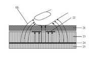
- FIG. 2shows an implementation principle of a capacitive touch sensor according to an embodiment of the present invention.
- a driving electrode layer 24 with one or multiple driving electrodesis closely layed out on a bottom surface of an insulating isolation layer 23 .
- a sensing electrode layer 22 with one or multiple sensing electrodesis closely layed out on a top surface of the insulating isolation layer 23 .
- a touch panel 21is configured above the sensing electrode layer 22 .
- a substrate 25is optionally configured on a bottom surface of the driving electrode layer 24 .
- the sensing electrode layer 22has hollowed-out regions.
- the capacitance change rate caused by touching the detection pointcan be increased by increasing the difference between C 0 and C T , so as to improve detection control circuits to detect and recognize the touch operation.
- ⁇is a dielectric constant
- Sis an overlapping area of the top and bottom substrates
- kis an electrostatic constant
- dis a distance between the top and bottom substrates.
- the value of the capacitor Cis linearly proportional to the overlapping area of the parallel plate capacitor.
- the capacitor formed by the driving electrode layer and the sensing electrode layeris a non-standard parallel plate capacitor, but the capacitance is still proportional to the overlapping area.
- the overlapping area between the driving electrode and the sensing electrodeis decreased and the initial capacitance C 0 is thereby decreased, by hollowing out the sensing electrode layer.
- the sensing electrode layer 22is hollowed-out, more electric field lines between the driving electrode layer 24 and the sensing electrode layer 22 can be extended beyond the overlapping area than those in conventional capacitive touch sensors. Thus, more electric field lines can be touched by finger, and a larger change in capacitance can be caused, that is, the value of C 0 ⁇ C T is increased. Therefore, the capacitance change rate of the capacitive touch sensor as shown in FIG. 2 is increased largely when the capacitive touch sensor is touched by finger; this means that sensitivity of the capacitive touch sensor is also improved.
- each sensing electrode of the sensing electrode layer 22fully overlaps a driving electrode of the driving electrode layer 24 , so that the sensing electrode can be shielded against interference from a lower component such as an LCD by the overlapped driving electrode.
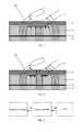
- FIG. 3is a block diagram of a touch detection device using the above-mentioned capacitive touch sensor of the present invention.
- a touch controller of the touch detection deviceis configured for scanning detection and control, processing and calculating sampled data, and further outputting a coordinate to an upper CPU.
- the upper CPUprocesses the received coordinate.
- FIGS. 4A ⁇ 4Care respectively schematic diagrams of an entire screen structure, a sensing electrode layer and a driving electrode layer of a multi-touch capacitive structure which can be realized by the above-mentioned technology.
- the experimentsprove that the capacitive structure has advantages of small initial capacitance at the detection point, large capacitance change rate when touched by finger, strong detected signal data, high sensitivity, and greatly improved signal to noise ratio (SNR) of the detection data.
- SNRsignal to noise ratio
- FIG. 5is a schematic diagram, partially showing a driving electrode layer and leads A of the driving electrode layer according to an embodiment of the present invention.
- FIG. 6Ais a schematic diagram, partially showing a sensing electrode layer having diamond pattern sensing electrodes with hollowed-out regions, leads B 1 of the sensing electrode layer, and suspended blocks C 1 according to an embodiment of the present invention.
- FIG. 6Bis a schematic assembled view of a structure including the driving electrodes of FIG. 5 and the sensing electrodes of FIG. 6A .
- FIG. 7Ais a schematic diagram, partially showing a sensing electrode layer having diamond pattern sensing electrodes with hollowed-out regions, leads B 2 of the sensing electrode layer and suspended blocks C 2 , according to another embodiment of the present invention.
- FIG. 7Bis a schematic assembled view of a structure including the driving electrodes of FIG. 5 and the sensing electrodes of FIG. 7A .
- FIG. 8Ais a schematic diagram, partially showing a sensing electrode layer having rectangular pattern sensing electrodes with hollowed-out regions, leads B 3 of the sensing electrode layer and suspended blocks C 3 , according to an embodiment of the present invention.
- FIG. 7Ais a schematic diagram, partially showing a sensing electrode layer having rectangular pattern sensing electrodes with hollowed-out regions, leads B 3 of the sensing electrode layer and suspended blocks C 3 , according to an embodiment of the present invention.
- FIG. 8Bis a schematic assembled view of a structure including the driving electrodes of FIG. 5 and the sensing electrodes of FIG. 8A .
- FIG. 9Ais a schematic diagram, partially showing a sensing electrode layer having round pattern sensing electrodes with hollowed-out regions, leads B 4 of the sensing electrode layer and suspended blocks C 4 , according to an embodiment of the present invention.
- FIG. 9Bis a schematic assembled view of a structure including the driving electrodes of FIG. 5 and the sensing electrodes of FIG. 9A .
- FIG. 10Ais a schematic diagram, partially showing a sensing electrode layer having hexagonal pattern sensing electrodes with hollowed-out regions, leads B 5 of the sensing electrode layer and suspended blocks C 5 , according to an embodiment of the present invention.
- FIG. 9Ais a schematic diagram, partially showing a sensing electrode layer having hexagonal pattern sensing electrodes with hollowed-out regions, leads B 5 of the sensing electrode layer and suspended blocks C 5 , according to an embodiment of the present
- each sensing electrodecan have only one hollowed-out region as exemplarily shown in FIG. 8A , or have multiple hollowed-out regions separate from each other as exemplarily shown in FIG. 6A , FIG. 7A , FIG. 9A and FIG. 10A .
- the initial capacitancecan be adjusted by adjusting the area of the hollowed-out regions, for adapting to different situations, such as the capacitive touch sensors with different thickness.
- a distance between the driving electrode layer and the sensing electrode layeris relatively shorter.
- the initial capacitance C 0is thus increased and the capacitance change rate is thus reduced.
- the area of the hollowed-out regionscan be increased to reduce the overlapping area between the driving electrode layer and the sensing electrode layer.
- the initial capacitanceis reduced to counteract the negative impact of the small capacitance change rate caused by the short distance between the driving electrode layer and the sensing electrode layer.
- capacitive touch sensorscan be used in touch detection devices, or directly used in various capacitive touch terminals, such as capacitive touch button control terminals, capacitive touch slider control terminals, capacitive touch wheel control terminals or capacitive touch screen terminals.
Landscapes
- Engineering & Computer Science (AREA)
- General Engineering & Computer Science (AREA)
- Theoretical Computer Science (AREA)
- Human Computer Interaction (AREA)
- Physics & Mathematics (AREA)
- General Physics & Mathematics (AREA)
- Quality & Reliability (AREA)
- Position Input By Displaying (AREA)
Abstract
Description
δ=(C0−CT)/C0 (1)
C=∈S/(4πkd) (2)
Claims (4)
Applications Claiming Priority (4)
| Application Number | Priority Date | Filing Date | Title |
|---|---|---|---|
| CN20102011486.1 | 2010-02-04 | ||
| CN2010201104861UCN201622554U (en) | 2010-02-04 | 2010-02-04 | Capacitance touch sensor, touch detection device, and touch control terminal |
| CN201020110486U | 2010-02-24 | ||
| PCT/CN2011/070673WO2011095102A1 (en) | 2010-02-04 | 2011-01-26 | Capacitive type touch sensor, touch detection device and touch control terminal |
Related Parent Applications (1)
| Application Number | Title | Priority Date | Filing Date |
|---|---|---|---|
| PCT/CN2011/070673ContinuationWO2011095102A1 (en) | 2010-02-04 | 2011-01-26 | Capacitive type touch sensor, touch detection device and touch control terminal |
Publications (2)
| Publication Number | Publication Date |
|---|---|
| US20110187676A1 US20110187676A1 (en) | 2011-08-04 |
| US8803823B2true US8803823B2 (en) | 2014-08-12 |
Family
ID=43026013
Family Applications (1)
| Application Number | Title | Priority Date | Filing Date |
|---|---|---|---|
| US13/069,405Active2031-06-26US8803823B2 (en) | 2010-02-04 | 2011-03-23 | Capacitive touch sensor, touch detection device and touch terminal |
Country Status (4)
| Country | Link |
|---|---|
| US (1) | US8803823B2 (en) |
| KR (1) | KR200483031Y1 (en) |
| CN (1) | CN201622554U (en) |
| WO (1) | WO2011095102A1 (en) |
Cited By (14)
| Publication number | Priority date | Publication date | Assignee | Title |
|---|---|---|---|---|
| US20140111222A1 (en)* | 2012-10-19 | 2014-04-24 | Microchip Technology Incorporated | Electrode Design for Electric Field Measurement System |
| US9069411B2 (en) | 2010-12-30 | 2015-06-30 | Egalax—Empia Technology Inc. | Capacitive touch screen |
| USD735175S1 (en)* | 2013-01-30 | 2015-07-28 | Htc Corporation | Display module for an electronic device |
| USD735176S1 (en)* | 2013-01-30 | 2015-07-28 | Htc Corporation | Display module for an electronic device |
| US9639734B1 (en) | 2015-11-13 | 2017-05-02 | Cypress Semiconductor Corporation | Fingerprint sensor-compatible overlay material |
| US9811206B2 (en) | 2014-10-21 | 2017-11-07 | Industrial Technology Research Institute | Touch sensing method, touch display apparatus and portable electronic device |
| US9823796B2 (en) | 2014-03-25 | 2017-11-21 | Hailiang Wang | Systems and methods for touch sensors on polymer lenses |
| US10282585B2 (en) | 2015-11-13 | 2019-05-07 | Cypress Semiconductor Corporation | Sensor-compatible overlay |
| US10294422B2 (en) | 2015-07-16 | 2019-05-21 | Hailiang Wang | Etching compositions for transparent conductive layers comprising silver nanowires |
| US10372246B2 (en) | 2015-07-16 | 2019-08-06 | Hailiang Wang | Transferable nanocomposites for touch sensors |
| US10747372B2 (en) | 2015-03-25 | 2020-08-18 | Hailiang Wang | Systems and high throughput methods for touch sensors |
| US10817087B2 (en)* | 2016-07-12 | 2020-10-27 | Hailiang Wang | Transferable nanocomposites for touch sensors |
| US10832029B2 (en) | 2015-11-13 | 2020-11-10 | Cypress Semiconductor Corporation | Sensor-compatible overlay |
| US11520421B2 (en) | 2017-09-29 | 2022-12-06 | Samsung Display Co., Ltd. | Display device and method of driving the same |
Families Citing this family (59)
| Publication number | Priority date | Publication date | Assignee | Title |
|---|---|---|---|---|
| KR101073684B1 (en)* | 2009-08-25 | 2011-10-14 | 주식회사 지니틱스 | Transparent Electrode Pattern Of Capacitive Touch Screen For Low Resistance |
| CN201622554U (en)* | 2010-02-04 | 2010-11-03 | 深圳市汇顶科技有限公司 | Capacitance touch sensor, touch detection device, and touch control terminal |
| TWI426437B (en) | 2010-10-28 | 2014-02-11 | Young Lighting Technology Inc | Capacitive touch panel |
| CN102467303B (en)* | 2010-11-04 | 2014-09-03 | 扬升照明股份有限公司 | Capacitive touch panel |
| TWI421756B (en)* | 2010-12-23 | 2014-01-01 | Au Optronics Corp | Touch display panel and touch sensing panel |
| JP5806684B2 (en)* | 2011-01-11 | 2015-11-10 | アルプス電気株式会社 | Coordinate input device |
| CN102367982A (en)* | 2011-10-09 | 2012-03-07 | 广东美的电器股份有限公司 | Air conditioner and control method thereof |
| US20130154996A1 (en)* | 2011-12-16 | 2013-06-20 | Matthew Trend | Touch Sensor Including Mutual Capacitance Electrodes and Self-Capacitance Electrodes |
| US9634660B2 (en) | 2011-12-20 | 2017-04-25 | Atmel Corporation | Touch sensor with reduced anti-touch effects |
| KR101893111B1 (en) | 2012-01-04 | 2018-08-31 | 삼성디스플레이 주식회사 | Display device including sensor |
| US20130176262A1 (en)* | 2012-01-05 | 2013-07-11 | Silicon Integrated Systems Corp. | Projected capacitive touch panel |
| CN103207712B (en)* | 2012-01-13 | 2016-04-13 | 江西沃格光电股份有限公司 | Capacitive touch screen and preparation technology thereof |
| KR101941507B1 (en) | 2012-02-10 | 2019-04-12 | 삼성전자주식회사 | Apparatus and method for compensating touch error in electronic device with touch screen |
| TWI531948B (en)* | 2012-03-14 | 2016-05-01 | 宏達國際電子股份有限公司 | Touch panel |
| US8895882B2 (en)* | 2012-03-14 | 2014-11-25 | Htc Corporation | Touch panel |
| CN102662544A (en)* | 2012-03-31 | 2012-09-12 | 苏州瀚瑞微电子有限公司 | Double-layer ITO (indium tin oxide) wire arrangement structure |
| CN102662516A (en)* | 2012-03-31 | 2012-09-12 | 苏州瀚瑞微电子有限公司 | Touch screen electrode layout |
| KR101385438B1 (en) | 2012-06-12 | 2014-04-15 | 삼성디스플레이 주식회사 | Touch screen panel |
| CN102750039A (en)* | 2012-06-29 | 2012-10-24 | 苏州瀚瑞微电子有限公司 | Wiring structure of touch screen |
| CN102778972B (en)* | 2012-06-29 | 2016-08-10 | 苏州瀚瑞微电子有限公司 | A kind of wire structures of double-deck ITO |
| CN103576998B (en)* | 2012-07-20 | 2017-07-28 | 上海思立微电子科技有限公司 | Capacitive touch screen and single layer cloth line electrode array |
| TWI472973B (en)* | 2012-08-20 | 2015-02-11 | Sitronix Technology Corp | Touch electrode module and its touch device |
| CN102968226B (en)* | 2012-08-29 | 2017-05-31 | 北京集创北方科技股份有限公司 | A kind of double-layer capacitive touch screen |
| TW201413519A (en)* | 2012-09-27 | 2014-04-01 | Wintek Corp | Touch panel and touch display panel |
| CN102915170B (en)* | 2012-10-26 | 2016-06-22 | 苏州瀚瑞微电子有限公司 | A kind of electrode lay-out of touch screen |
| CN102945098B (en)* | 2012-11-29 | 2016-05-11 | 苏州瀚瑞微电子有限公司 | A kind of electrode lay-out of touch-screen |
| CN103970313A (en)* | 2013-01-25 | 2014-08-06 | 深圳欧菲光科技股份有限公司 | Touch inducing element and touch screen |
| CN103135862A (en)* | 2013-03-04 | 2013-06-05 | 敦泰科技有限公司 | Capacitive touch screen and electronic device |
| US9035906B2 (en)* | 2013-03-13 | 2015-05-19 | Synaptics Incorporated | Proximity sensing |
| US9557866B2 (en)* | 2013-03-15 | 2017-01-31 | Beijing Boe Optoelectronics Technology Co., Ltd. | Capacitive touch panel and touch display apparatus |
| CN104102331B (en)* | 2013-04-08 | 2017-07-07 | 宏碁股份有限公司 | Touch panel input analysis system and method |
| CN103309503B (en)* | 2013-05-17 | 2016-03-02 | 北京京东方光电科技有限公司 | A kind of touch-screen and display device |
| CN103455225A (en)* | 2013-08-15 | 2013-12-18 | 深圳欧菲光科技股份有限公司 | Capacitive touch component and touch device |
| CN104423754A (en)* | 2013-09-11 | 2015-03-18 | 比亚迪股份有限公司 | Touch detection assembly, touch control device and portable electronic equipment |
| CN103472951B (en)* | 2013-09-13 | 2016-10-05 | 京东方科技集团股份有限公司 | A kind of touch screen and preparation method thereof, display device |
| CN103543895A (en)* | 2013-09-30 | 2014-01-29 | 领威联芯(北京)科技有限公司 | Electrode device of touch screen and mutual capacitance touch screen using electrode device |
| JP6233075B2 (en)* | 2014-02-06 | 2017-11-22 | 大日本印刷株式会社 | Touch panel sensor and input / output device including touch panel sensor |
| US10098198B2 (en)* | 2014-04-03 | 2018-10-09 | Ford Global Technologies, Llc | Interior ambient and task light bars |
| EP3130984B1 (en)* | 2014-04-07 | 2019-09-04 | Murata Manufacturing Co., Ltd. | Touch panel and electronic device |
| EP2958000B1 (en)* | 2014-05-30 | 2018-04-11 | Marvell World Trade Ltd. | Touch panel and touch detection circuit |
| US20150370404A1 (en)* | 2014-06-23 | 2015-12-24 | Touchplus Information Corp. | Multi-phase touch-sensing electronic device |
| CN104536629B (en) | 2015-01-16 | 2019-03-26 | 京东方科技集团股份有限公司 | A kind of In-cell touch panel and display device |
| CN104777940B (en)* | 2015-04-30 | 2017-11-14 | 京东方科技集团股份有限公司 | A kind of touch control electrode layer and touch-screen |
| TWI658384B (en)* | 2015-05-29 | 2019-05-01 | 巴貝多商馬維爾國際貿易有限公司 | Touch panel and touch detection circuit |
| CN205427802U (en)* | 2016-02-26 | 2016-08-03 | 意力(广州)电子科技有限公司 | Touch screen |
| US10588202B1 (en)* | 2016-05-02 | 2020-03-10 | Technology For Humankind Llc | Communicative lighting systems |
| CN106325641A (en)* | 2016-08-29 | 2017-01-11 | 红河以恒科技集团有限公司 | Touch electrode structure, touch panel and touch display |
| CN106339142A (en)* | 2016-08-29 | 2017-01-18 | 贵州乾盛科技有限公司 | Touch electrode structure, touch panel and touch display device |
| CN106325640A (en)* | 2016-08-29 | 2017-01-11 | 红河以恒科技集团有限公司 | Touch electrode structure, touch panel and touch display device |
| KR102811755B1 (en) | 2017-02-03 | 2025-05-23 | 삼성디스플레이 주식회사 | Touch sensor and display device having the touch sensor |
| KR101932650B1 (en) | 2017-05-15 | 2018-12-28 | 삼성디스플레이 주식회사 | Touch sensor and display device having the touch sensor |
| KR102044801B1 (en)* | 2017-06-20 | 2019-11-15 | 주식회사 하이딥 | Touch sensor panel |
| KR102424954B1 (en)* | 2017-08-07 | 2022-07-26 | 삼성디스플레이 주식회사 | Input sensing unit and display device having the same |
| CN108037846B (en)* | 2017-11-30 | 2021-02-26 | 广州国显科技有限公司 | Touch display panel, preparation method thereof and touch display device |
| WO2019105051A1 (en)* | 2017-11-30 | 2019-06-06 | 云谷(固安)科技有限公司 | Touch display panel and preparation method therefor, and touch display device |
| WO2019105050A1 (en)* | 2017-11-30 | 2019-06-06 | 云谷(固安)科技有限公司 | Touch control display panel and touch control display apparatus |
| US20190245011A1 (en)* | 2018-02-06 | 2019-08-08 | Innolux Corporation | Display device |
| CN109742100B (en)* | 2018-12-18 | 2020-08-04 | 武汉华星光电半导体显示技术有限公司 | Display panel |
| CN111327306B (en)* | 2020-02-26 | 2023-03-21 | 业成科技(成都)有限公司 | Touch button and operating handle |
Citations (3)
| Publication number | Priority date | Publication date | Assignee | Title |
|---|---|---|---|---|
| US20090213090A1 (en)* | 2008-02-27 | 2009-08-27 | Norio Mamba | Display Panel |
| US8269743B2 (en)* | 2009-03-02 | 2012-09-18 | Au Optronics Corporation | Touch sensing display panel and touch sensing substrate |
| US8279187B2 (en)* | 2008-08-01 | 2012-10-02 | 3M Innovative Properties Company | Touch sensitive devices with composite electrodes |
Family Cites Families (10)
| Publication number | Priority date | Publication date | Assignee | Title |
|---|---|---|---|---|
| GB0519170D0 (en)* | 2005-09-20 | 2005-10-26 | Philipp Harald | Capacitive touch sensor |
| US7932898B2 (en)* | 2005-09-20 | 2011-04-26 | Atmel Corporation | Touch sensitive screen |
| KR100791102B1 (en)* | 2006-08-16 | 2008-01-02 | (주)휴엔텍 | Touchpad type remote control |
| CN100495139C (en)* | 2007-10-10 | 2009-06-03 | 友达光电股份有限公司 | Touch panel and manufacturing method thereof |
| JP4816668B2 (en)* | 2008-03-28 | 2011-11-16 | ソニー株式会社 | Display device with touch sensor |
| CN101303635A (en)* | 2008-07-01 | 2008-11-12 | 友达光电股份有限公司 | Capacitive touch panel and manufacturing method thereof |
| CN101393502B (en)* | 2008-10-31 | 2012-03-07 | 敦泰科技有限公司 | Mutual capacitance touch screen and combined mutual capacitance touch screen |
| CN101424817B (en)* | 2008-12-17 | 2010-07-21 | 友达光电股份有限公司 | Method for manufacturing color filtering touch substrate |
| CN101441538B (en)* | 2008-12-19 | 2010-11-10 | 友达光电股份有限公司 | Structure of touch control type apparatus and touch control type display panel |
| CN201622554U (en)* | 2010-02-04 | 2010-11-03 | 深圳市汇顶科技有限公司 | Capacitance touch sensor, touch detection device, and touch control terminal |
- 2010
- 2010-02-04CNCN2010201104861Upatent/CN201622554U/ennot_activeExpired - Lifetime
- 2011
- 2011-01-26KRKR2020127000044Upatent/KR200483031Y1/ennot_activeExpired - Lifetime
- 2011-01-26WOPCT/CN2011/070673patent/WO2011095102A1/enactiveApplication Filing
- 2011-03-23USUS13/069,405patent/US8803823B2/enactiveActive
Patent Citations (3)
| Publication number | Priority date | Publication date | Assignee | Title |
|---|---|---|---|---|
| US20090213090A1 (en)* | 2008-02-27 | 2009-08-27 | Norio Mamba | Display Panel |
| US8279187B2 (en)* | 2008-08-01 | 2012-10-02 | 3M Innovative Properties Company | Touch sensitive devices with composite electrodes |
| US8269743B2 (en)* | 2009-03-02 | 2012-09-18 | Au Optronics Corporation | Touch sensing display panel and touch sensing substrate |
Cited By (20)
| Publication number | Priority date | Publication date | Assignee | Title |
|---|---|---|---|---|
| US9069411B2 (en) | 2010-12-30 | 2015-06-30 | Egalax—Empia Technology Inc. | Capacitive touch screen |
| US9459296B2 (en)* | 2012-10-19 | 2016-10-04 | Microchip Technology Germany Gmbh Ii & Co. Kg | Electrode design for electric field measurement system |
| US20160322971A1 (en)* | 2012-10-19 | 2016-11-03 | Microchip Technology Germany Gmbh Ii & Co. Kg | Electrode Design For Electric Field Measurement System |
| US10873330B2 (en) | 2012-10-19 | 2020-12-22 | Microchip Technology Germany Gmbh Ii & Co. Kg | Electrode design for electric field measurement system |
| US20140111222A1 (en)* | 2012-10-19 | 2014-04-24 | Microchip Technology Incorporated | Electrode Design for Electric Field Measurement System |
| USD735175S1 (en)* | 2013-01-30 | 2015-07-28 | Htc Corporation | Display module for an electronic device |
| USD735176S1 (en)* | 2013-01-30 | 2015-07-28 | Htc Corporation | Display module for an electronic device |
| US9823796B2 (en) | 2014-03-25 | 2017-11-21 | Hailiang Wang | Systems and methods for touch sensors on polymer lenses |
| US9811206B2 (en) | 2014-10-21 | 2017-11-07 | Industrial Technology Research Institute | Touch sensing method, touch display apparatus and portable electronic device |
| US10747372B2 (en) | 2015-03-25 | 2020-08-18 | Hailiang Wang | Systems and high throughput methods for touch sensors |
| US10372246B2 (en) | 2015-07-16 | 2019-08-06 | Hailiang Wang | Transferable nanocomposites for touch sensors |
| US10294422B2 (en) | 2015-07-16 | 2019-05-21 | Hailiang Wang | Etching compositions for transparent conductive layers comprising silver nanowires |
| US10282585B2 (en) | 2015-11-13 | 2019-05-07 | Cypress Semiconductor Corporation | Sensor-compatible overlay |
| US10235558B2 (en) | 2015-11-13 | 2019-03-19 | Cypress Semiconductor Corporation | Fingerprint sensor-compatible overlay material |
| US10832029B2 (en) | 2015-11-13 | 2020-11-10 | Cypress Semiconductor Corporation | Sensor-compatible overlay |
| US9639734B1 (en) | 2015-11-13 | 2017-05-02 | Cypress Semiconductor Corporation | Fingerprint sensor-compatible overlay material |
| US10817087B2 (en)* | 2016-07-12 | 2020-10-27 | Hailiang Wang | Transferable nanocomposites for touch sensors |
| US11520421B2 (en) | 2017-09-29 | 2022-12-06 | Samsung Display Co., Ltd. | Display device and method of driving the same |
| US11640211B2 (en) | 2017-09-29 | 2023-05-02 | Samsung Display Co., Ltd. | Display device and method of driving the same |
| US12079411B2 (en) | 2017-09-29 | 2024-09-03 | Samsung Display Co., Ltd. | Display device and method of driving the same |
Also Published As
| Publication number | Publication date |
|---|---|
| WO2011095102A1 (en) | 2011-08-11 |
| CN201622554U (en) | 2010-11-03 |
| US20110187676A1 (en) | 2011-08-04 |
| KR200483031Y1 (en) | 2017-03-27 |
| KR20120007716U (en) | 2012-11-08 |
Similar Documents
| Publication | Publication Date | Title |
|---|---|---|
| US8803823B2 (en) | Capacitive touch sensor, touch detection device and touch terminal | |
| KR101542043B1 (en) | Touch screen panel | |
| US8829926B2 (en) | Transparent proximity sensor | |
| US10402000B2 (en) | Display with integrated pressure sensing utilizing capacitive coupling to circuit elements | |
| CN104216584B (en) | Touch-control display panel and display device | |
| TWI408580B (en) | Projective capacitive touch sensor | |
| US10025433B2 (en) | Touch display device and method for manufacturing the same | |
| US20110100727A1 (en) | Touch Sensitive Device with Dielectric Layer | |
| US20130088448A1 (en) | Touch screen panel | |
| TWI630537B (en) | Touch display system with pressure sensing | |
| CN103116431B (en) | Self-capacitance touch screen and electronic equipment | |
| WO2014190672A1 (en) | Array substrate, touch panel, and display apparatus | |
| US20100231531A1 (en) | Touch panel device | |
| CN101738765B (en) | Liquid crystal display panel and device integrated with touch screen and touch detection method | |
| CN103513825A (en) | touch device | |
| CN102662513B (en) | Sensing structure of touch panel | |
| US9298330B2 (en) | Capacitive touch panel having complementarily matching adjacent electrode units and display device including the capacitive touch panel | |
| CN107728863A (en) | touch display panel | |
| CN106125975A (en) | A kind of contact panel and preparation method thereof, contactor control device | |
| US20120092295A1 (en) | Touch-Sensitive Coordinate Input Apparatus, Touch Panel and Electronic Devices Having the Same | |
| CN104571767A (en) | Touch panel, display device and touch drive method | |
| KR20120035744A (en) | Touch screen panel of electric capacity type having via hole and method of manufacturing the same | |
| CN114077363A (en) | Balanced mutual capacitance system and method | |
| WO2018201728A1 (en) | Touch control substrate and touchscreen | |
| WO2015080891A1 (en) | Methods and apparatus for arranging electrode layers and associated routing traces in a sensor device |
Legal Events
| Date | Code | Title | Description |
|---|---|---|---|
| AS | Assignment | Owner name:SHENZHEN GOODIX TECHNOLOGY CO., LTD., CHINA Free format text:ASSIGNMENT OF ASSIGNORS INTEREST;ASSIGNORS:CHANG, HAO;DENG, GENGCHUN;REEL/FRAME:026000/0920 Effective date:20110301 | |
| AS | Assignment | Owner name:SHENZHEN HUIDING TECHNOLOGY CO., LTD., CHINA Free format text:CHANGE OF NAME;ASSIGNOR:SHENZHEN GOODIX TECHNOLOGY CO., LTD.;REEL/FRAME:030490/0818 Effective date:20120920 | |
| STCF | Information on status: patent grant | Free format text:PATENTED CASE | |
| MAFP | Maintenance fee payment | Free format text:PAYMENT OF MAINTENANCE FEE, 4TH YR, SMALL ENTITY (ORIGINAL EVENT CODE: M2551) Year of fee payment:4 | |
| AS | Assignment | Owner name:SHENZHEN GOODIX TECHNOLOGY CO., LTD., CHINA Free format text:ASSIGNMENT OF ASSIGNORS INTEREST;ASSIGNOR:SHENZHEN HUIDING TECHNOLOGY CO., LTD.;REEL/FRAME:045855/0977 Effective date:20180226 | |
| FEPP | Fee payment procedure | Free format text:ENTITY STATUS SET TO UNDISCOUNTED (ORIGINAL EVENT CODE: BIG.); ENTITY STATUS OF PATENT OWNER: LARGE ENTITY | |
| MAFP | Maintenance fee payment | Free format text:PAYMENT OF MAINTENANCE FEE UNDER 1.28(C) (ORIGINAL EVENT CODE: M1559); ENTITY STATUS OF PATENT OWNER: LARGE ENTITY | |
| FEPP | Fee payment procedure | Free format text:PETITION RELATED TO MAINTENANCE FEES GRANTED (ORIGINAL EVENT CODE: PTGR); ENTITY STATUS OF PATENT OWNER: LARGE ENTITY | |
| MAFP | Maintenance fee payment | Free format text:PAYMENT OF MAINTENANCE FEE, 8TH YEAR, LARGE ENTITY (ORIGINAL EVENT CODE: M1552); ENTITY STATUS OF PATENT OWNER: LARGE ENTITY Year of fee payment:8 |