US8802545B2 - Method and apparatus for plasma dicing a semi-conductor wafer - Google Patents
Method and apparatus for plasma dicing a semi-conductor waferDownload PDFInfo
- Publication number
- US8802545B2 US8802545B2US13/412,119US201213412119AUS8802545B2US 8802545 B2US8802545 B2US 8802545B2US 201213412119 AUS201213412119 AUS 201213412119AUS 8802545 B2US8802545 B2US 8802545B2
- Authority
- US
- United States
- Prior art keywords
- substrate
- plasma
- work piece
- time division
- division multiplex
- Prior art date
- Legal status (The legal status is an assumption and is not a legal conclusion. Google has not performed a legal analysis and makes no representation as to the accuracy of the status listed.)
- Active
Links
Images


Classifications
- H—ELECTRICITY
- H01—ELECTRIC ELEMENTS
- H01J—ELECTRIC DISCHARGE TUBES OR DISCHARGE LAMPS
- H01J37/00—Discharge tubes with provision for introducing objects or material to be exposed to the discharge, e.g. for the purpose of examination or processing thereof
- H01J37/32—Gas-filled discharge tubes
- H01J37/32431—Constructional details of the reactor
- H01J37/32623—Mechanical discharge control means
- H—ELECTRICITY
- H01—ELECTRIC ELEMENTS
- H01J—ELECTRIC DISCHARGE TUBES OR DISCHARGE LAMPS
- H01J37/00—Discharge tubes with provision for introducing objects or material to be exposed to the discharge, e.g. for the purpose of examination or processing thereof
- H01J37/32—Gas-filled discharge tubes
- H01J37/32009—Arrangements for generation of plasma specially adapted for examination or treatment of objects, e.g. plasma sources
- H01J37/32082—Radio frequency generated discharge
- H01J37/321—Radio frequency generated discharge the radio frequency energy being inductively coupled to the plasma
- H—ELECTRICITY
- H01—ELECTRIC ELEMENTS
- H01J—ELECTRIC DISCHARGE TUBES OR DISCHARGE LAMPS
- H01J37/00—Discharge tubes with provision for introducing objects or material to be exposed to the discharge, e.g. for the purpose of examination or processing thereof
- H01J37/32—Gas-filled discharge tubes
- H01J37/32009—Arrangements for generation of plasma specially adapted for examination or treatment of objects, e.g. plasma sources
- H01J37/32082—Radio frequency generated discharge
- H01J37/32137—Radio frequency generated discharge controlling of the discharge by modulation of energy
- H01J37/32155—Frequency modulation
- H—ELECTRICITY
- H01—ELECTRIC ELEMENTS
- H01J—ELECTRIC DISCHARGE TUBES OR DISCHARGE LAMPS
- H01J37/00—Discharge tubes with provision for introducing objects or material to be exposed to the discharge, e.g. for the purpose of examination or processing thereof
- H01J37/32—Gas-filled discharge tubes
- H01J37/32431—Constructional details of the reactor
- H01J37/32623—Mechanical discharge control means
- H01J37/32642—Focus rings
- H—ELECTRICITY
- H01—ELECTRIC ELEMENTS
- H01J—ELECTRIC DISCHARGE TUBES OR DISCHARGE LAMPS
- H01J37/00—Discharge tubes with provision for introducing objects or material to be exposed to the discharge, e.g. for the purpose of examination or processing thereof
- H01J37/32—Gas-filled discharge tubes
- H01J37/32431—Constructional details of the reactor
- H01J37/32623—Mechanical discharge control means
- H01J37/32651—Shields, e.g. dark space shields, Faraday shields
- H—ELECTRICITY
- H01—ELECTRIC ELEMENTS
- H01J—ELECTRIC DISCHARGE TUBES OR DISCHARGE LAMPS
- H01J37/00—Discharge tubes with provision for introducing objects or material to be exposed to the discharge, e.g. for the purpose of examination or processing thereof
- H01J37/32—Gas-filled discharge tubes
- H01J37/32431—Constructional details of the reactor
- H01J37/32715—Workpiece holder
- H01J37/32724—Temperature
- H—ELECTRICITY
- H01—ELECTRIC ELEMENTS
- H01L—SEMICONDUCTOR DEVICES NOT COVERED BY CLASS H10
- H01L21/00—Processes or apparatus adapted for the manufacture or treatment of semiconductor or solid state devices or of parts thereof
- H01L21/02—Manufacture or treatment of semiconductor devices or of parts thereof
- H01L21/04—Manufacture or treatment of semiconductor devices or of parts thereof the devices having potential barriers, e.g. a PN junction, depletion layer or carrier concentration layer
- H01L21/18—Manufacture or treatment of semiconductor devices or of parts thereof the devices having potential barriers, e.g. a PN junction, depletion layer or carrier concentration layer the devices having semiconductor bodies comprising elements of Group IV of the Periodic Table or AIIIBV compounds with or without impurities, e.g. doping materials
- H01L21/30—Treatment of semiconductor bodies using processes or apparatus not provided for in groups H01L21/20 - H01L21/26
- H01L21/302—Treatment of semiconductor bodies using processes or apparatus not provided for in groups H01L21/20 - H01L21/26 to change their surface-physical characteristics or shape, e.g. etching, polishing, cutting
- H01L21/306—Chemical or electrical treatment, e.g. electrolytic etching
- H01L21/3065—Plasma etching; Reactive-ion etching
- H01L21/30655—Plasma etching; Reactive-ion etching comprising alternated and repeated etching and passivation steps, e.g. Bosch process
- H—ELECTRICITY
- H01—ELECTRIC ELEMENTS
- H01L—SEMICONDUCTOR DEVICES NOT COVERED BY CLASS H10
- H01L21/00—Processes or apparatus adapted for the manufacture or treatment of semiconductor or solid state devices or of parts thereof
- H01L21/67—Apparatus specially adapted for handling semiconductor or electric solid state devices during manufacture or treatment thereof; Apparatus specially adapted for handling wafers during manufacture or treatment of semiconductor or electric solid state devices or components ; Apparatus not specifically provided for elsewhere
- H01L21/67005—Apparatus not specifically provided for elsewhere
- H01L21/67011—Apparatus for manufacture or treatment
- H01L21/67017—Apparatus for fluid treatment
- H01L21/67063—Apparatus for fluid treatment for etching
- H01L21/67069—Apparatus for fluid treatment for etching for drying etching
- H—ELECTRICITY
- H01—ELECTRIC ELEMENTS
- H01L—SEMICONDUCTOR DEVICES NOT COVERED BY CLASS H10
- H01L21/00—Processes or apparatus adapted for the manufacture or treatment of semiconductor or solid state devices or of parts thereof
- H01L21/67—Apparatus specially adapted for handling semiconductor or electric solid state devices during manufacture or treatment thereof; Apparatus specially adapted for handling wafers during manufacture or treatment of semiconductor or electric solid state devices or components ; Apparatus not specifically provided for elsewhere
- H01L21/68—Apparatus specially adapted for handling semiconductor or electric solid state devices during manufacture or treatment thereof; Apparatus specially adapted for handling wafers during manufacture or treatment of semiconductor or electric solid state devices or components ; Apparatus not specifically provided for elsewhere for positioning, orientation or alignment
- H—ELECTRICITY
- H01—ELECTRIC ELEMENTS
- H01L—SEMICONDUCTOR DEVICES NOT COVERED BY CLASS H10
- H01L21/00—Processes or apparatus adapted for the manufacture or treatment of semiconductor or solid state devices or of parts thereof
- H01L21/67—Apparatus specially adapted for handling semiconductor or electric solid state devices during manufacture or treatment thereof; Apparatus specially adapted for handling wafers during manufacture or treatment of semiconductor or electric solid state devices or components ; Apparatus not specifically provided for elsewhere
- H01L21/683—Apparatus specially adapted for handling semiconductor or electric solid state devices during manufacture or treatment thereof; Apparatus specially adapted for handling wafers during manufacture or treatment of semiconductor or electric solid state devices or components ; Apparatus not specifically provided for elsewhere for supporting or gripping
- H01L21/6831—Apparatus specially adapted for handling semiconductor or electric solid state devices during manufacture or treatment thereof; Apparatus specially adapted for handling wafers during manufacture or treatment of semiconductor or electric solid state devices or components ; Apparatus not specifically provided for elsewhere for supporting or gripping using electrostatic chucks
- H01L21/6833—Details of electrostatic chucks
- H—ELECTRICITY
- H01—ELECTRIC ELEMENTS
- H01L—SEMICONDUCTOR DEVICES NOT COVERED BY CLASS H10
- H01L21/00—Processes or apparatus adapted for the manufacture or treatment of semiconductor or solid state devices or of parts thereof
- H01L21/67—Apparatus specially adapted for handling semiconductor or electric solid state devices during manufacture or treatment thereof; Apparatus specially adapted for handling wafers during manufacture or treatment of semiconductor or electric solid state devices or components ; Apparatus not specifically provided for elsewhere
- H01L21/683—Apparatus specially adapted for handling semiconductor or electric solid state devices during manufacture or treatment thereof; Apparatus specially adapted for handling wafers during manufacture or treatment of semiconductor or electric solid state devices or components ; Apparatus not specifically provided for elsewhere for supporting or gripping
- H01L21/687—Apparatus specially adapted for handling semiconductor or electric solid state devices during manufacture or treatment thereof; Apparatus specially adapted for handling wafers during manufacture or treatment of semiconductor or electric solid state devices or components ; Apparatus not specifically provided for elsewhere for supporting or gripping using mechanical means, e.g. chucks, clamps or pinches
- H01L21/68714—Apparatus specially adapted for handling semiconductor or electric solid state devices during manufacture or treatment thereof; Apparatus specially adapted for handling wafers during manufacture or treatment of semiconductor or electric solid state devices or components ; Apparatus not specifically provided for elsewhere for supporting or gripping using mechanical means, e.g. chucks, clamps or pinches the wafers being placed on a susceptor, stage or support
- H01L21/68735—Apparatus specially adapted for handling semiconductor or electric solid state devices during manufacture or treatment thereof; Apparatus specially adapted for handling wafers during manufacture or treatment of semiconductor or electric solid state devices or components ; Apparatus not specifically provided for elsewhere for supporting or gripping using mechanical means, e.g. chucks, clamps or pinches the wafers being placed on a susceptor, stage or support characterised by edge profile or support profile
- H—ELECTRICITY
- H01—ELECTRIC ELEMENTS
- H01L—SEMICONDUCTOR DEVICES NOT COVERED BY CLASS H10
- H01L21/00—Processes or apparatus adapted for the manufacture or treatment of semiconductor or solid state devices or of parts thereof
- H01L21/67—Apparatus specially adapted for handling semiconductor or electric solid state devices during manufacture or treatment thereof; Apparatus specially adapted for handling wafers during manufacture or treatment of semiconductor or electric solid state devices or components ; Apparatus not specifically provided for elsewhere
- H01L21/683—Apparatus specially adapted for handling semiconductor or electric solid state devices during manufacture or treatment thereof; Apparatus specially adapted for handling wafers during manufacture or treatment of semiconductor or electric solid state devices or components ; Apparatus not specifically provided for elsewhere for supporting or gripping
- H01L21/687—Apparatus specially adapted for handling semiconductor or electric solid state devices during manufacture or treatment thereof; Apparatus specially adapted for handling wafers during manufacture or treatment of semiconductor or electric solid state devices or components ; Apparatus not specifically provided for elsewhere for supporting or gripping using mechanical means, e.g. chucks, clamps or pinches
- H01L21/68714—Apparatus specially adapted for handling semiconductor or electric solid state devices during manufacture or treatment thereof; Apparatus specially adapted for handling wafers during manufacture or treatment of semiconductor or electric solid state devices or components ; Apparatus not specifically provided for elsewhere for supporting or gripping using mechanical means, e.g. chucks, clamps or pinches the wafers being placed on a susceptor, stage or support
- H01L21/68742—Apparatus specially adapted for handling semiconductor or electric solid state devices during manufacture or treatment thereof; Apparatus specially adapted for handling wafers during manufacture or treatment of semiconductor or electric solid state devices or components ; Apparatus not specifically provided for elsewhere for supporting or gripping using mechanical means, e.g. chucks, clamps or pinches the wafers being placed on a susceptor, stage or support characterised by a lifting arrangement, e.g. lift pins
- H—ELECTRICITY
- H01—ELECTRIC ELEMENTS
- H01L—SEMICONDUCTOR DEVICES NOT COVERED BY CLASS H10
- H01L21/00—Processes or apparatus adapted for the manufacture or treatment of semiconductor or solid state devices or of parts thereof
- H01L21/70—Manufacture or treatment of devices consisting of a plurality of solid state components formed in or on a common substrate or of parts thereof; Manufacture of integrated circuit devices or of parts thereof
- H01L21/77—Manufacture or treatment of devices consisting of a plurality of solid state components or integrated circuits formed in, or on, a common substrate
- H01L21/78—Manufacture or treatment of devices consisting of a plurality of solid state components or integrated circuits formed in, or on, a common substrate with subsequent division of the substrate into plural individual devices
- H—ELECTRICITY
- H01—ELECTRIC ELEMENTS
- H01J—ELECTRIC DISCHARGE TUBES OR DISCHARGE LAMPS
- H01J37/00—Discharge tubes with provision for introducing objects or material to be exposed to the discharge, e.g. for the purpose of examination or processing thereof
- H01J37/32—Gas-filled discharge tubes
- H01J37/32009—Arrangements for generation of plasma specially adapted for examination or treatment of objects, e.g. plasma sources
- H01J37/32422—Arrangement for selecting ions or species in the plasma
- H—ELECTRICITY
- H01—ELECTRIC ELEMENTS
- H01L—SEMICONDUCTOR DEVICES NOT COVERED BY CLASS H10
- H01L21/00—Processes or apparatus adapted for the manufacture or treatment of semiconductor or solid state devices or of parts thereof
- H01L21/02—Manufacture or treatment of semiconductor devices or of parts thereof
- H01L21/04—Manufacture or treatment of semiconductor devices or of parts thereof the devices having potential barriers, e.g. a PN junction, depletion layer or carrier concentration layer
- H01L21/18—Manufacture or treatment of semiconductor devices or of parts thereof the devices having potential barriers, e.g. a PN junction, depletion layer or carrier concentration layer the devices having semiconductor bodies comprising elements of Group IV of the Periodic Table or AIIIBV compounds with or without impurities, e.g. doping materials
- H01L21/30—Treatment of semiconductor bodies using processes or apparatus not provided for in groups H01L21/20 - H01L21/26
- H01L21/31—Treatment of semiconductor bodies using processes or apparatus not provided for in groups H01L21/20 - H01L21/26 to form insulating layers thereon, e.g. for masking or by using photolithographic techniques; After treatment of these layers; Selection of materials for these layers
- H01L21/3105—After-treatment
- H01L21/311—Etching the insulating layers by chemical or physical means
- H01L21/31105—Etching inorganic layers
- H01L21/31111—Etching inorganic layers by chemical means
- H01L21/31116—Etching inorganic layers by chemical means by dry-etching
- H—ELECTRICITY
- H01—ELECTRIC ELEMENTS
- H01L—SEMICONDUCTOR DEVICES NOT COVERED BY CLASS H10
- H01L21/00—Processes or apparatus adapted for the manufacture or treatment of semiconductor or solid state devices or of parts thereof
- H01L21/67—Apparatus specially adapted for handling semiconductor or electric solid state devices during manufacture or treatment thereof; Apparatus specially adapted for handling wafers during manufacture or treatment of semiconductor or electric solid state devices or components ; Apparatus not specifically provided for elsewhere
- H01L21/677—Apparatus specially adapted for handling semiconductor or electric solid state devices during manufacture or treatment thereof; Apparatus specially adapted for handling wafers during manufacture or treatment of semiconductor or electric solid state devices or components ; Apparatus not specifically provided for elsewhere for conveying, e.g. between different workstations
- H01L21/67739—Apparatus specially adapted for handling semiconductor or electric solid state devices during manufacture or treatment thereof; Apparatus specially adapted for handling wafers during manufacture or treatment of semiconductor or electric solid state devices or components ; Apparatus not specifically provided for elsewhere for conveying, e.g. between different workstations into and out of processing chamber
- H—ELECTRICITY
- H01—ELECTRIC ELEMENTS
- H01L—SEMICONDUCTOR DEVICES NOT COVERED BY CLASS H10
- H01L2221/00—Processes or apparatus adapted for the manufacture or treatment of semiconductor or solid state devices or of parts thereof covered by H01L21/00
- H01L2221/67—Apparatus for handling semiconductor or electric solid state devices during manufacture or treatment thereof; Apparatus for handling wafers during manufacture or treatment of semiconductor or electric solid state devices or components; Apparatus not specifically provided for elsewhere
- H01L2221/683—Apparatus for handling semiconductor or electric solid state devices during manufacture or treatment thereof; Apparatus for handling wafers during manufacture or treatment of semiconductor or electric solid state devices or components; Apparatus not specifically provided for elsewhere for supporting or gripping
- H01L2221/68304—Apparatus for handling semiconductor or electric solid state devices during manufacture or treatment thereof; Apparatus for handling wafers during manufacture or treatment of semiconductor or electric solid state devices or components; Apparatus not specifically provided for elsewhere for supporting or gripping using temporarily an auxiliary support
- H01L2221/68327—Apparatus for handling semiconductor or electric solid state devices during manufacture or treatment thereof; Apparatus for handling wafers during manufacture or treatment of semiconductor or electric solid state devices or components; Apparatus not specifically provided for elsewhere for supporting or gripping using temporarily an auxiliary support used during dicing or grinding
- Y—GENERAL TAGGING OF NEW TECHNOLOGICAL DEVELOPMENTS; GENERAL TAGGING OF CROSS-SECTIONAL TECHNOLOGIES SPANNING OVER SEVERAL SECTIONS OF THE IPC; TECHNICAL SUBJECTS COVERED BY FORMER USPC CROSS-REFERENCE ART COLLECTIONS [XRACs] AND DIGESTS
- Y10—TECHNICAL SUBJECTS COVERED BY FORMER USPC
- Y10S—TECHNICAL SUBJECTS COVERED BY FORMER USPC CROSS-REFERENCE ART COLLECTIONS [XRACs] AND DIGESTS
- Y10S414/00—Material or article handling
- Y10S414/135—Associated with semiconductor wafer handling
- Y10S414/139—Associated with semiconductor wafer handling including wafer charging or discharging means for vacuum chamber
Definitions
- the inventionrelates to the use of an apparatus for the formation of individual device chips from a semi-conductor wafer, and in particular to an apparatus which uses plasma etching to separate the wafer into individual die.
- Semi-conductor devicesare fabricated on substrates which are in the form of thin wafers. Silicon is commonly used as the substrate material, but other materials, such as III-V compounds (for example GaAs and InP) are also used.
- the substrateis a sapphire or silicon carbide wafer on which a thin layer of a semi-conducting material is deposited.
- the size of such substratesranges from 2 inches and 3 inches up to 200 mm, 300 mm, and 450 mm diameter and many standards exist (e.g., SEMI) to describe such substrate sizes.
- Plasma etching equipmentis used extensively in the processing of these substrates to produce semi-conductor devices.
- Such equipmenttypically includes a vacuum chamber fitted with a high density plasma source such as Inductively Coupled Plasma (ICP) which is used to ensure high etch rates, necessary for cost-effective manufacturing.
- ICPInductively Coupled Plasma
- the substrateis typically clamped to a cooled support.
- a cooling gastypically Helium
- a mechanical clamping mechanismin which a downward force is applied to the top side of the substrate, may be used, though this may cause contamination due to the contact between the clamp and the substrate. More frequently an Electrostatic chuck (ESC) is used to provide the clamping force.
- ESCElectrostatic chuck
- halogenFluorine, Chlorine, Bromine, or Iodine
- halogen-containing gassuch as SF 6 , F 2 or NF 3 are used to etch silicon at a high rate.
- a processBosch or TDM which alternates a high rate silicon etch step with a passivation step to control the etch sidewall, is commonly used to etch deep features into silicon.
- Chlorine and Bromine containing gasesare commonly used to etch III-V materials.
- Plasma etchingis not limited to semiconducting substrates and devices.
- the techniquemay be applied to any substrate type where a suitable gas chemistry to etch the substrate is available.
- Other substrate typesmay include carbon containing substrates (including polymeric substrates), ceramic substrates (e.g., AlTiC and sapphire), metal substrates, and glass substrates.
- Handlersare designed to support the wafers with minimal contact, to minimize possible contamination and reduce the generation of particulates. Edge contact alone, or underside contact close to the wafer edge at only a few locations (typically within 3-6 mm of the wafer edge) is generally employed. Handling schemes, which include wafer cassettes, robotic arms and within process chamber fixtures including the wafer support and ESC, are designed to handle the standard wafer sizes as noted previously.
- the individual devicesare separated from each other prior to packaging or being employed in other electronic circuitry.
- mechanical meanshave been used to separate the die from each other. Such mechanical means have included breaking the wafer along scribe lines aligned with the substrate crystal axis or by using a high speed diamond saw to saw into or through the substrate in a region (streets) between the die. More recently, lasers have been used to facilitate the scribing process.
- Such mechanical wafer dicing techniqueshave limitations which affect the cost effectiveness of this approach. Chipping and breakage along the die edges can reduce the number of good die produced, and becomes more problematic as wafer thicknesses decrease.
- the area consumed by the saw bade (kerf)may be greater than 100 microns which is valuable area not usable for die production.
- kerfsaw bade
- For wafers containing small diee.g., individual semiconductor devices with a die size of 500 microns ⁇ 500 microns
- thiscan represent a loss of greater than 20%.
- the dicing timeis increased, and productivity decreased, since each street is cut individually.
- Mechanical meansare also limited to separation along straight lines and the production of square or oblong shaped chips.
- Laser dicingalso has limitations by leaving residual material on the die surface or inducing stress into the die.
- the kerf dimensionscan be reduced to well below 20 microns
- Die topologyis not limited to a rectilinear format.
- the substratemay be thinned by mechanical grinding or similar process down to a thickness of a few hundred microns, or even less than a hundred microns.
- the substratePrior to the dicing process, the substrate is typically mounted on a dicing fixture.
- This fixtureis typically comprised of a rigid frame that supports an adhesive membrane. The substrate to be diced is adhered to the membrane. This fixture holds the separated die for subsequent downstream operations.
- Most tools used for wafer dicingsaws or laser based tools
- current automated plasma etching equipmentis not suitable for processing substrates fixtured for dicing and it is difficult to realize the benefits that plasma etch techniques should have for die separation.
- U.S. Pat. No. 6,642,127describes a plasma dicing technique in which the substrate wafer is first attached to a carrier wafer via an adhesive material, before plasma processing in equipment designed for processing silicon wafers.
- This techniqueproposes adapting the form factor of the substrate to be diced to be compatible with standard wafer processing equipment. While this technique allows standard plasma equipment to dice the wafer, the proposed technique will not be compatible with standard equipment downstream of the dicing operation. Additional steps would be required to either adapt the downstream equipment or revert the substrate form factor for standard downstream equipment.
- U.S. Patent Application 2010/0048001contemplates the use of a wafer adhered to a thin membrane and supported within a frame.
- the masking processis achieved by adhering a mask material to the backside of the wafer and using a laser to define the etch streets prior to plasma processing.
- this techniqueintroduces additional complex and expensive steps which may negate some of the advantages of plasma dicing. It also requires the additional demand of aligning the backside mask with the front side device pattern.
- a plasma etching apparatuswhich can be used for dicing a semiconductor substrate into individual die and which is compatible with the established wafer dicing technique of handling a substrate mounted on tape and supported in a frame, and which is also compatible with standard front side masking techniques.
- Another object of the present inventionis to provide a method for plasma dicing a substrate, the method comprising: providing a process chamber having a wall; providing a plasma source adjacent to the wall of the process chamber; providing a work piece support within the process chamber; placing the substrate on a carrier support to form a work piece; loading the work piece onto the work piece support; providing a cover ring disposed above the work piece; generating a plasma through the plasma source; and etching the work piece through the generated plasma.
- Yet another object of the present inventionis to provide a method for plasma dicing a substrate, the method comprising: providing a process chamber having a wall; providing a plasma source adjacent to the wall of the process chamber; providing a work piece support within the process chamber, the work piece support having an electrostatic chuck; placing the substrate on a carrier support to form a work piece; loading the work piece onto the work piece support; clamping the work piece to the work piece support through the electrostatic chuck; providing a cover ring disposed above the work piece; generating a plasma through the plasma source; etching the work piece through the generated plasma; and controlling temperature of the cover ring during the etching step.
- Still yet another object of the present inventionis to provide a method for plasma dicing a substrate, the method comprising: placing the substrate on a carrier support to form a work piece; loading the work piece into a plasma processing chamber; exposing the work piece in the plasma processing chamber to a first plasma etch process using a first etchant gas; terminating the first plasma etch process after singulation; and exposing the work piece in the plasma processing chamber to a second plasma etch process using a second etchant gas.
- Another object of the present inventionis to provide an apparatus for plasma dicing a substrate comprising: a process chamber having a wall; a plasma source adjacent to the wall of the process chamber; a work piece support within the process chamber, the work piece support having an electrostatic chuck; a work piece having the substrate on a carrier support, the work piece being placed onto the work piece support; and a cover ring disposed above the work piece, the cover ring is thermally coupled to the wall of the process chamber.
- the present inventiondescribes a plasma processing apparatus which allows for plasma dicing of a semiconductor substrate.
- the front side (circuit side) of the substrateis masked using conventional masking techniques which protects the circuit components and leaves unprotected areas between the die.
- the substrateis mounted on a thin tape which is supported within a rigid frame.
- the substrate/tape/frame assemblyis transferred into a vacuum processing chamber and exposed to reactive gas plasma where the unprotected areas between the die are etched away. During this process, the frame and tape are protected from damage by the reactive gas plasma.
- the processingleaves the die completely separated.
- the substrate/tape/frame assemblyis additionally exposed to plasma which removes potentially damaging residues from the substrate surface.
- the dieare removed from the tape using well known techniques and are then further processed (e.g., packaged) as necessary.
- the substratecan have a semiconducting layer such as Silicon and/or the substrate can have a III-V layer such as GaAs.
- the substratecan have a protective layer such as a photoresist layer that is patterned on a circuit side of the substrate.
- a process chamber having a wall with a plasma source adjacent to the wall of the process chamberis provided.
- the plasma sourcecan be a high density plasma source.
- a vacuum pump in fluid communication with the process chamber and a gas inlet in fluid communication with the process chambercan be provided.
- a work piece support within the process chamberis provided. A work piece is formed by placing the substrate on a carrier support.
- the work piececan be formed by adhering the substrate to a support film and then mounting the substrate with the support film to a frame.
- the support filmcan have a polymer layer and/or a conductive layer.
- the support filmcan be standard dicing tape.
- the framecan have a conductive layer and/or a metal layer.
- An RF power sourcecan be coupled to the work piece support to create a plasma around the work piece.
- a thermal communication between the work piece and the work piece supportcan be provided by supplying a pressurized gas such as helium from the work piece support to the work piece.
- An electrostatic chuckcan be incorporated into the work piece support whereby the electrostatic chuck can clamp the support film to the electrostatic chuck.
- the electrostatic chuckcan have monopolar or multipolar clamping electrodes and provide a clamping force through either a coulombic or Johnsen-Rahbek effect.
- the electrostatic chuckcan have a diameter that is greater than a diameter of the substrate.
- the electrostatic chuckcan have a diameter that is less than an inner diameter of the frame.
- the electrostatic chuckcan have a flat top surface.
- the electrostatic chuckcan have features that are less than a singulated die size.
- a lifting mechanismcan be incorporated into the work piece support where the work piece is loaded onto the lifting mechanism. The lifting mechanism can be designed so that it only touches the frame of the work piece.
- a filler ringcan be provided where the filler ring extends from an outer diameter of the electrostatic chuck to the lifting mechanism.
- the filler ringcan be made from a dielectric material.
- a mechanical partitioncan be provided between the high density source and the work piece.
- the partitioncan be a screen that can be conductive that can be made of aluminum.
- a cover ringis disposed above the work piece.
- An inner diameter of the cover ringcan be less than an outer diameter of the substrate.
- the pressure within the process chambercan be reduced through the vacuum pump and a process gas can be introduced into the process chamber through the gas inlet.
- a plasmais generated through the plasma source whereby the work piece is etched through the generated plasma.
- the temperature of the cover ringcan be controlled during the plasma etching step. During the plasma etching step, the cover ring can be cooled to a temperature of less than 80° C.
- the cover ringcan be cooled by using the wall of the process chamber and/or a heat sink.
- the cover ringcan be temperature controlled by contacting a temperature controlled fluid.
- the cover ringcan have a plurality of holes, a plasma resistant layer, a metal layer and/or a ceramic layer.
- a vacuum compatible transfer modulecan be provided that communicates with the process chamber.
- the work piececan be loaded onto a transfer arm in the vacuum compatible transfer module whereby the process chamber is maintained under vacuum during a transfer of the work piece from the vacuum compatible transfer module to the process chamber.
- the transfer armcan be flat, indexed to the frame, only contact the frame and/or remain substantially coplanar to the substrate during transfer.
- the work piececan be aligned prior to transfer into the process chamber by a mechanical alignment and/or an optical alignment.
- the frame and/or the substratecan be aligned prior to transfer into the process chamber.
- the substratecan have a semiconducting layer such as Silicon and/or the substrate can have a III-V layer such as GaAs.
- the substratecan have a protective layer such as a photoresist layer that is patterned on a circuit side of the substrate.
- a process chamber having a wall with a plasma source adjacent to the wall of the process chamberis provided.
- the plasma sourcecan be a high density plasma source.
- a vacuum pump in fluid communication with the process chamber and a gas inlet in fluid communication with the process chambercan be provided.
- a work piece support within the process chamberis provided. A work piece is formed by placing the substrate on a carrier support.
- the work piececan be formed by adhering the substrate to a support film and then mounting the substrate with the support film to a frame.
- the support filmcan have a polymer layer and/or a conductive layer.
- the support filmcan be standard dicing tape.
- the framecan have a conductive layer and/or a metal layer.
- An RF power sourcecan be coupled to the work piece support to create a plasma around the work piece.
- a thermal communication between the work piece and the work piece supportcan be provided by supplying a pressurized gas such as helium from the work piece support to the work piece.
- An electrostatic chuckis incorporated into the work piece support whereby the electrostatic chuck clamps the work piece to the electrostatic chuck.
- the electrostatic chuckcan be monopolar or multi-polar.
- the electrostatic chuckcan clamp the substrate using a coulombic or Johnsen-Rahbek effect.
- the electrostatic chuckcan have a diameter that is greater than a diameter of the substrate.
- the electrostatic chuckcan have a diameter that is less than an inner diameter of the frame.
- the electrostatic chuckcan have a flat top surface.
- the electrostatic chuckcan have features that are less than a singulated die size.
- a lifting mechanismcan be incorporated into the work piece support where the work piece is loaded onto the lifting mechanism. The lifting mechanism can be designed so that it only touches the frame of the work piece.
- a filler ringcan be provided where the filler ring extends from an outer diameter of the electrostatic chuck to the lifting mechanism.
- the filler ringcan be made from a dielectric material.
- a mechanical partitioncan be provided between the high density source and the work piece.
- the partitioncan be a screen that can be conductive that can be made of aluminum.
- a cover ringis disposed above the work piece.
- An inner diameter of the cover ringcan be less than an outer diameter of the substrate.
- the pressure within the process chambercan be reduced through the vacuum pump and a process gas can be introduced into the process chamber through the gas inlet.
- a plasmais generated through the plasma source whereby the work piece is etched through the generated plasma.
- the temperature of the cover ringis controlled during the plasma etching step. During the plasma etching step, the cover ring can be cooled to a temperature of less than 80° C.
- the cover ringcan be cooled by using the wall of the process chamber and/or a heat sink.
- the cover ringcan have a plurality of holes, a plasma resistant layer, a metal layer and/or a ceramic layer.
- a vacuum compatible transfer modulecan be provided that communicates with the process chamber.
- the work piececan be loaded onto a transfer arm in the vacuum compatible transfer module whereby the process chamber is maintained under vacuum during a transfer of the work piece from the vacuum compatible transfer module to the process chamber.
- the transfer armcan be flat, indexed to the frame, only contact the frame and/or remain coplanar to the substrate during transfer.
- the work piececan be aligned prior to transfer into the process chamber by a mechanical alignment and/or an optical alignment.
- the frame and/or the substratecan be aligned prior to transfer into the process chamber.
- Still yet another feature of the present inventionis to provide a method for plasma dicing a substrate.
- a work pieceis formed by placing the substrate on a carrier support.
- the work piececan be formed by adhering the substrate to a support film and then mounting the substrate with the support film to a frame.
- the support filmcan have a polymer layer and/or a conductive layer.
- the support filmcan be standard dicing tape.
- the framecan have a conductive layer and/or a metal layer.
- the work pieceis loaded into a plasma processing chamber.
- a cover ringcan be disposed above the work piece.
- the work pieceis exposed to a first plasma etch process using a first etchant gas within the plasma processing chamber.
- the first etchant gascan be a halogen containing gas such as a Fluorine containing gas or a Chlorine containing gas.
- the first etch processcan be a time division multiplexed etch process.
- the first plasma etch processis terminated after the die are singulated. The termination of the first plasma etch process can occur at an interface between the substrate and the support film which can be determined using a standard endpoint technique.
- the work piececan be exposed to a second plasma etch process using a second etchant gas within the plasma processing chamber.
- the second plasma etch processcan be a lower etch rate process designed to reduce undercut.
- the second etchant gascan be a second halogen containing gas such as a Fluorine containing gas or a Chlorine containing gas.
- the second etch processcan be a second time division multiplexed etch process.
- the work piececan be exposed to a third plasma etch process using a third etchant gas within the plasma processing chamber.
- the third plasma etch processcan remove unwanted residues that exist on devices after exposure to the first plasma etch process and/or second plasma etch process.
- the third etchant gascan be a hydrogen containing gas.
- Another feature of the present inventionis to provide an apparatus for plasma dicing a substrate comprising a process chamber having a wall with a plasma source adjacent to the wall of the process chamber.
- the plasma sourcecan be a high density plasma source.
- the process chambercan have a vacuum pump in fluid communication with the process chamber and a gas inlet in fluid communication with the process chamber.
- a work piece support within the process chamberwhich has an electrostatic chuck.
- a work piece having the substrate mounted on a carrier supportis placed onto the work piece support.
- the work piececan have the substrate on a support film which is then mounted on a frame.
- the support filmcan have a polymer layer and/or a conductive layer.
- the support filmcan be standard dicing tape.
- the framecan have a conductive layer and/or a metal layer.
- a cover ringis disposed above the work piece and the cover ring is thermally coupled to the wall of the process chamber and/or a heat sink.
- the cover ringcan have a plurality of holes.
- a mechanical partitioncan be placed between the high density source and the work piece.
- a lifting mechanismcan be placed within the work piece support.
- a filler ring that extends from an outer diameter of the electrostatic chuck to the lifting mechanismcan be included.
- FIG. 1is a top down view of a semiconductor substrate illustrating individual devices separated by streets;
- FIG. 2is a cross-sectional view of a semiconductor substrate illustrating individual devices separated by streets;
- FIG. 3is a cross-sectional view of a semiconductor substrate mounted to tape and a frame;
- FIG. 4is a cross-sectional view of a semiconductor substrate mounted to tape and a frame being etched by a plasma process
- FIG. 5is a cross-sectional view of separated semiconductor devices mounted to tape and a frame
- FIG. 6is a cross-sectional view of a vacuum processing chamber
- FIG. 7is a cross-sectional of a wafer/frame in process position
- FIG. 8is an enlarged cross-sectional view of a frame and a cover ring in a vacuum processing chamber
- FIG. 9is a cross-sectional view of a section of the inside the chamber with the cover ring mounted to a chamber wall;
- FIG. 10is a cross-sectional view of a section of the inside the chamber with the cover ring mounted to an internal heat sink;
- FIG. 11is a top down view of a semiconductor substrate mounted to tape and a frame supported by a transfer arm;
- FIG. 12is a cross-sectional view of a semiconductor substrate mounted to tape and a frame supported by a transfer arm;
- FIG. 13is a cross-sectional view of a wafer/frame in a transfer position
- FIG. 14is a top view of a screen
- FIG. 15is a cross-sectional view of an electrostatic chuck.
- FIG. 16is a schematic view of a chamber in a transfer position.
- FIG. 1A typical semiconductor substrate after device fabrication is illustrated in FIG. 1 .
- the substrate ( 1 )has on its surface a number of areas containing device structures ( 2 ) separated by street areas ( 3 ) in which there are no structures which allows for separation of the device structures into individual die.
- siliconis commonly used as a substrate material, other materials chosen for their particular characteristics are frequently employed.
- substrate materialsinclude gallium arsenide and other III-V materials or non-semi-conductor substrates on which has been deposited a semi-conducting layer.
- the device structures ( 2 )are then covered with a protective material ( 4 ) while the street areas ( 3 ) remain unprotected.
- This protective material ( 4 )can be a photoresist, applied and patterned by well-known techniques.
- Some devices, as a final process stepare coated with a protective dielectric layer such as silicon dioxide or PSG which is applied across the whole substrate. This can be selectively removed from the street areas ( 3 ) by patterning with photoresist and etching the dielectric material, as is well known in the industry. This leaves the device structures ( 2 ) protected by the dielectric material and the substrate ( 1 ) substantially unprotected in the street areas ( 3 ).
- test features to check the wafer qualitymay be located in the street areas ( 3 ). Depending on the specific wafer fabrication process flow, these test features may or may not be protected during the wafer dicing process.
- the device pattern illustratedshows oblong die, this is not necessary, and the individual device structures ( 2 ) may be any other shape, such as hexagons, as best suits the optimum utilization of the substrate ( 1 ).
- the protective filmcan consist of multiple materials. It is also important to note that some portion of the protective film may be an integral part of the final device structure. (e.g., a passivation dielectric, metal bonding pad, etc.)
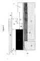
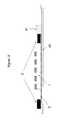
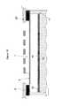
- the substrate ( 1 )may be thinned, typically by a grinding process, which reduces the substrate thickness to a few hundred microns to as thin as approximately 30 microns or less. As is shown in FIG. 3 , the thinned substrate ( 1 ) is then adhered to a tape ( 5 ) which in turn is mounted in a rigid frame ( 6 ) to form a work piece ( 1 A).
- the tape ( 5 )is typically made from a carbon-containing polymer material, and may additionally have a thin conductive layer applied to its surface. The tape ( 5 ) provides support for the thinned substrate ( 1 ) which is otherwise too fragile to handle without breakage.
- the sequence of patterning, thinning and then mountingis not critical and the steps may be adjusted to best fit the particular devices and substrate and the processing equipment used. It is important to note that while the previous example considers a work piece ( 1 A) that is comprised of mounting a substrate ( 1 ) on an adhesive tape ( 5 ) which in turn is attached to a frame ( 6 ), that the invention is not limited by the configuration of the wafer and carrier.
- the wafer carriercan be comprised a variety of materials.
- the carriersupports the substrate during the plasma dicing process.
- the waferneed not be attached to the carrier using an adhesive—any method that holds the wafer to the carrier and allows a means thermal communication of the substrate to the cathode is sufficient. (e.g. an electrostatically clamped carrier, a carrier with a mechanical clamping mechanism, etc.)
- the transfer moduleis also under vacuum which allows the process chamber to remain at vacuum during transfer, reducing processing time and preventing exposure of the process chamber to atmosphere and possible contamination. As shown in FIG.
- the vacuum processing chamber ( 10 )is equipped with a gas inlet ( 11 ), a high density plasma source ( 12 ) to generate a high density plasma, such as an Inductively Coupled Plasma (ICP), a work piece support ( 13 ) to support the work piece ( 1 A), an RF power source ( 14 ) to couple RF power to the work piece ( 1 A) through the work piece support ( 13 ) and a vacuum pump ( 15 ) for pumping gas from the processing chamber ( 10 ).
- ICPInductively Coupled Plasma
- a work piece support ( 13 )to support the work piece ( 1 A)
- an RF power source ( 14 )to couple RF power to the work piece ( 1 A) through the work piece support ( 13 )
- a vacuum pump ( 15 )for pumping gas from the processing chamber ( 10 ).
- the unprotected areas of substrate ( 1 )are etched away using a reactive plasma etch process ( 7 ) as shown in FIG. 4 . This leaves the devices ( 2 ) separated into
- the unprotected areas of the substrate ( 1 )are partially etched away using a reactive plasma etch process ( 7 ).
- a downstream operationsuch as a mechanical breaking operation, can be used to complete the die separation.
- the frame ( 6 )When the substrate/tape/frame assembly ( 1 A) is in the position for plasma processing, it is important that the frame ( 6 ) is protected from exposure to the plasma ( 7 ). Exposure to the plasma ( 7 ) will cause heating of the frame ( 6 ) which in turn will cause local heating of the mounting tape ( 5 ). At temperatures above approximately 100° C., the physical properties of the tape ( 5 ) and its adhesive capability may deteriorate and it will no longer adhere to the frame ( 6 ). Additionally, exposure of the frame ( 6 ) to the reactive plasma gas may cause degradation of the frame ( 6 ). Since the frame ( 6 ) is typically re-used after wafer dicing, this may limit the useful lifetime of a frame ( 6 ).
- Exposure of the frame ( 6 ) to the plasma ( 7 )may also adversely affect the etch process: for example the frame material may react with the process gas, effectively reducing its concentration in the plasma which will reduce the etch rate of the substrate material, thus increasing process time.
- a protective cover ring ( 20 )is positioned above the frame ( 6 ). The cover ring ( 20 ) does not touch the frame ( 6 ) since contact with the frame ( 6 ) (which would occur during transfer into the process chamber ( 10 )) can generate undesirable particles.
- dimension (A)represents the distance between the cover ring ( 20 ) and the frame ( 6 ). This dimension can range from greater than approximately 0.5 mm to less than approximately 5 mm with an optimal value of 1.5 mm. If the distance (A) is too large, plasma ( 7 ) will contact the frame ( 6 ) and the benefits of the cover ring ( 20 ) will be lost.
- the cover ring ( 20 )is temperature controlled, otherwise its temperature will increase due to exposure to the plasma ( 7 ) and in turn heat the tape ( 5 ) and the frame ( 6 ) via radiational heating, causing degradation as noted above.
- cooling of the cover ring ( 20 )is accomplished by having it in direct contact with a cooled body, such as the process chamber wall ( 10 W) shown in FIG. 9 or a heat sink ( 30 ) located within the process chamber ( 10 ) shown in FIG. 10 .
- the cover ring ( 20 )should be made of a material that has good thermal conductivity.
- Such materialsinclude many metals, for example Aluminum, but other thermally conductive materials, such as Aluminum Nitride and other ceramics can be used.
- the choice of the cover ring materialis chosen to be compatible with the plasma process gases used. While Aluminum is satisfactory for Fluorine based processes, an alternate material, such as Aluminum Nitride, or the addition of a protective coating, such as Aluminum Oxide may be necessary when Chlorine based processes are used. Operation temperature of the cover ring ( 20 ) during plasma processing is typically less than 80° C. which minimizes heat radiation to the tape ( 5 ) and the frame ( 6 ) and ensures that the tape ( 5 ) maintains its mechanical integrity.
- the cover ring ( 20 )may be temperature controlled by bringing the cover ring ( 20 ) into contact with a temperature controlled fluid.
- This fluidcan be a liquid or gas.
- the cover ring ( 20 )may contain a number of fluid channels to facilitate heat transfer. These fluid channels can be internal to the cover ring ( 20 ), externally attached, or some combination of the two.
- the cover ring ( 20 )can extend from the substrate diameter to the inner chamber diameter continuously.
- a plurality of holes ( 21 )can be added to the cover ring ( 20 ) which allows sufficient conductance of the process gas while still providing a path for heat removal from the cover ring ( 20 ).
- FIGS. 9 and 10a plurality of holes ( 21 ) arranged in a specific geometry is shown, but the density, size, pattern and symmetry of the holes ( 21 ) can vary depending on the process chamber ( 10 ) dimensions and the pumping conductance required.
- the substrate/tape/frame assembly ( 1 A)is transferred both into and out of the process chamber ( 10 ) by a transfer arm ( 40 ) that supports the frame ( 6 ) and substrate ( 1 ) so that they are maintained coplanar as shown in FIGS. 11 and 12 .
- the transfer arm ( 40 )may support both the tape ( 5 ) and the frame ( 6 ) or the frame ( 6 ) alone, but it is important that the assembly ( 1 A) not be supported beneath the substrate ( 1 ) area alone because of the fragile nature of thinned substrates ( 1 ).
- the transfer arm ( 40 )has an alignment fixture ( 41 ) attached to it that aligns the frame ( 6 ) in a repeatable position before being transferred into the process chamber ( 10 ).
- the frame ( 6 )can also be aligned by other techniques well-known in semiconductor processing (e.g., optical alignment).
- the alignmentcan also be performed on the substrate ( 1 ) by such well-known techniques. It is important that the substrate/tape/frame assembly ( 1 A) be aligned before placement within the process chamber ( 10 ) to avoid mis-processing as explained below.
- the dimension (D)represents the distance between the outer diameter of the substrate ( 1 ) and the inner diameter of the frame ( 6 ). This may be 20 mm to 30 mm (e.g., Disco Corporation dicing frame is 250 mm for 200 mm substrates, so that the dimension (D) is nominally 25 mm).
- the deviation of wafer ( 1 ) placementmay be as much as 2 mm so that dimension (E), which is the distance between the substrate ( 1 ) outer diameter and the inner diameter of the cover ring ( 20 ) can also vary from assembly to assembly by up to 2 mm.
- the cover ring ( 20 )will overlay the edge of the substrate ( 1 ). This point will be shadowed and prevented from etching, which can prevent die separation and cause problems in subsequent processing steps. Alignment of the substrate/tape/frame assembly ( 1 A) prior to transfer is required to prevent such problems. Further, to additionally ensure that dimension (E) is not less than zero, the cover ring inner diameter should be greater than the diameter of the substrate ( 1 ) with a preferred diameter 5 mm greater than the substrate (e.g., 205 mm cover ring inner diameter for 200 mm substrate). Dimension (F) in FIG. 8 represents the distance from the inner diameter of the cover ring ( 20 ) to the inner diameter of the frame ( 6 ).
- Alignment of the frame ( 6 ) prior to transfer into the process chamber ( 10 )ensures that (F) remains constant for the entire circumference around the substrate ( 1 ) and that any portion of tape ( 5 ) that is not contacted by the Electrostatic chuck (ESC) ( 16 ) is shadowed from the plasma ( 7 ).
- the substrate/tape/frame assembly ( 1 A)When the substrate/tape/frame assembly ( 1 A) is transferred into the process chamber ( 10 ), it is placed onto the lifting mechanism ( 17 ) and removed from the transfer arm ( 40 ). The reverse process occurs during transfer of the substrate/tape/frame assembly ( 1 A) out of the process chamber ( 10 ).
- the lifting mechanism ( 17 )touches the frame ( 6 ) area and provides no point contact to the substrate ( 1 ). Point contact to the substrate ( 1 ) can cause damage to the substrate ( 1 ), particularly after die separation and unloading of the substrate/tape/frame assembly ( 1 A), since the flexibility of the tape ( 5 ) would cause the die to contact each other and damage to occur.
- the frame ( 6 )shows the lifting mechanism ( 17 ) contacting the frame ( 6 ) from the underside: however the frame ( 6 ) can also be removed from the transfer arm ( 40 ) by contact with the top surface or outer diameter using a clamping device.
- the frame ( 6 ), the work piece support ( 13 ), and the cover ring ( 20 )move relative to each other. This can be accomplished by moving either the cover ring ( 20 ), the work piece support ( 13 ), or the lifting mechanism ( 17 ) or any combination of the three.
- a conductive screen ( 25 )(e.g., made from aluminum or aluminum coated with an appropriate plasma resistant coating) can be placed between the substrate ( 1 ) and the plasma ( 7 ). This will reduce ion bombardment on the substrate ( 1 ) and thus reduce heating of the substrate ( 1 ).
- FIG 14shows the screen ( 25 ) is provided with a plurality of holes ( 26 ) which still allows neutral species from the plasma ( 7 ) to reach the substrate ( 1 ) such that the etch rate is only slightly reduced. Holes ( 27 ) allow for mounting of the screen ( 25 ) to the processing chamber ( 10 ).
- ESCElectrostatic chuck
- Such ESCs ( 16 )are commonly used in semiconductor processing to apply downward force to the substrate ( 1 ) while a pressurized gas such as Helium is maintained between the substrate ( 1 ) and the electrode. This ensures that heat transfer can occur between the substrate ( 1 ) and the electrode, which is cooled.
- ESCs ( 16 )are the same diameter or smaller than the substrate ( 1 ) to prevent unwanted exposure of the ESC ( 16 ) surface to potentially corrosive plasma gases that can decrease the lifetime of the ESC ( 16 ).
- the area outside the diameter of the substrate ( 1 )is tape ( 5 ).
- FIG. 8shows the use of an ESC ( 16 ) that is made purposely larger than the substrate diameter so that any tape ( 5 ) which is exposed to the plasma in region (E) is also clamped and cooled. This diameter can be extended outwards to the outer diameter of the frame ( 6 ), but is preferred to be 2 mm less than the inner diameter of the frame ( 6 ).
- FIG. 8shows a filler ring ( 18 ) that extends from the outer diameter of the ESC ( 16 ) to the lifting mechanism ( 17 ).
- This filler ring ( 18 )is used to prevent the back surface of any exposed tape ( 5 ) from being contacted by the plasma ( 7 ).
- a separate filler ring ( 18 )is shown, an extension of the ESC ( 16 ) would also prevent plasma ( 7 ) exposure to the backside of the tape ( 5 ).
- the filler ring ( 18 )is typically made of a dielectric material, such as a ceramic (e.g., Aluminum Oxide) or a plastic material, (e.g., polytetrafluoroethylene (PTFE, Teflon)) selected for both its low thermal conductivity and its low electrical conductivity.
- Typical ESCs ( 16 ) used in semiconductor processinghave a pattern of shallow features fabricated on their surface to facilitate Helium distribution or to minimize contact with the backside of a substrate ( 1 ) to reduce particle formation. Such an ESC ( 16 ) can be used for plasma dicing when a substrate ( 1 ) is separated into multiple die, providing the feature dimensions on the ESC surface are smaller than the die size.
- the tapeWhen the die size approaches and becomes smaller than the ESC feature size, the tape will now conform to the features and flex, possibly causing the die to touch each other which can cause damage.
- the use of a substantially coplanar ESC surfaceeliminates this problem. Note that though the preceding example describes an ESC that cools the substrate, for some materials (e.g. approximately 180° C. for indium containing substrates) that require a higher temperature to facilitate the plasma etch process, a higher temperature controlled ESC ( 16 ) temperature may be desirable.
- a typical ESC ( 16 )(coulombic design of FIG. 15 ) consists of one or more electrodes ( 33 ) to which a high voltage ( 19 ) is applied, separated from the work piece support ( 13 ) by a thick insulating layer ( 32 ) and separated from the material to be clamped by a thin layer of dielectric material ( 34 ).
- the clamping force generated by electrostatic forcesincreases as the thickness of this dielectric layer ( 34 ) decreases and increases as the voltage applied increases.
- the thickness of the tape ( 5 )adds to the total dielectric thickness interposed between the electrode ( 33 ) and the substrate ( 1 ).
- This total thicknessshould not be determined primarily by the tape thickness, since this is likely to vary, resulting in a variable clamping performance. Rather the ESC dielectric ( 34 ) should be relatively thick (of the order of a few 100 microns) to maintain a clamping performance independent of tape thickness.
- a high clamping forcecan be achieved by operating at a high clamping voltage (up to approximately 10 kV).
- RF power ( 14 )is coupled to the substrate ( 1 ) to control ion bombardment on the substrate ( 1 ) and control the etch characteristics.
- the frequency of this RFmay vary from 100's of MHz down to a few hundred kHz.
- problems with the etch associated with charging of the insulating layerare well known. Such problems include localized severe undercutting at the substrate/insulator interface which is undesirable during die separation, since this affects the performance of the singulated die.
- charging problemscan be reduced by operating at low RF frequencies and additionally pulsing or modulating the RF power at low frequency.
- the RF coupling to the substrate ( 1 )is preferably via the one or more ESC electrodes, for example via a coupling capacitor ( 35 ) rather than via the RF powered work piece support ( 13 ).
- the ESC electrode or electrodesshould also be uniformly disposed behind the substrate ( 1 ). This is difficult to achieve if multiple electrodes are used, since the necessary gaps between the electrodes result in a local variation in the RF coupling which adversely affects the quality of the etch, particularly the undercutting at the substrate/tape interface.
- a preferred embodiment of the ESC designtherefore incorporates a so called monopolar design, in which a single electrode is used to provide the clamping force. Additionally, there should be as few as possible penetrations through this electrode (for example as for pin lifts) since these penetrations will also disturb the RF coupling and degrade the etch performance.
- the substratecan be processed using techniques well known in the semiconductor industry. Silicon substrates are generally processed using a Fluorine based chemistry such as SF 6 . SF 6 /O 2 chemistry is commonly used to etch Silicon because of its high rate and anisotropic profile. A disadvantage of this chemistry is its relatively low selectivity to masking material for example to photoresist which is 15-20:1. Alternatively a Timed Division Multiplex (TDM) process can be used which alternates between deposition and etching to produce highly anisotropic deep profiles.
- TDMTimed Division Multiplex
- an alternating process to etch Siliconuses a C 4 F 8 step to deposit polymer on all exposed surfaces of the Silicon substrate (i.e., mask surface, etch sidewalls and etch floor) and then an SF 6 step is used to selectively remove the polymer from the etch floor and then isotropically etch a small amount of silicon. The steps repeat until terminated.
- Such a TDM processcan produce anisotropic features deep into Silicon with selectivities to the masking layer of greater than 200:1. This then makes a TDM process the desired approach for plasma separation of Silicon substrates.
- the inventionis not limited to the use of fluorine containing chemistries or a time division multiplex (TDM) process.
- silicon substratesmay also be etched with Cl, HBr or I containing chemistries as is known in the art.
- III-V substratessuch as GaAs
- a Chlorine based chemistryis extensively used in the semiconductor industry.
- thinned GaAs substratesare mounted with the device side down onto a carrier, where they are then thinned and patterned with photoresist.
- the GaAsis etched away to expose electrical contacts to the front side circuitry.
- This well-known processcan also be used to separate the devices by the front side processing described in the above mentioned invention.
- Other semiconductor substrates and appropriate plasma processescan also be used for the separation of die in the above mentioned invention.
- the processcan be changed at the point at which the interface is exposed to a second process which has less tendency to undercut and is typically a lower etch rate process.
- the point in time at which the change takes placedepends upon the substrate thickness, which is likely to vary.
- the time at which the substrate/tape interface is reachedis detected using an endpoint technique.
- Optical techniques which monitor the plasma emissionare commonly used to detect endpoint and U.S. Pat. Nos. 6,982,175 and 7,101,805 describe such an endpoint technique which is appropriate to a TDM process.
- Aluminumis commonly used as an electrical contact for semiconductor devices and when exposed to Fluorine based plasmas a layer of AlF 3 is formed on its surface.
- AlF 3is nonvolatile under normal plasma processing conditions and is not pumped away from the substrate and out of the system and remains on the surface after processing.
- AlF 3 on Aluminumis a common cause of failure for devices because the bonding strength of wires to the electrical contacts is greatly reduced.
- Wet methodscan be used; however, this becomes difficult because of the fragile nature of the separated die, and the possible damage to the tape causing die release.
- the processcan be changed to a third process while the substrate is still within the vacuum chamber, to a process designed to remove any AlF 3 formed.
- U.S. Pat. No. 7,150,796describes a method for in-situ removal of AlF 3 using an Hydrogen based plasma. Likewise, an in-situ treatment can be used to remove other halogen-containing residues when other halogen-containing gases are used to etch the substrate.
Landscapes
- Engineering & Computer Science (AREA)
- Physics & Mathematics (AREA)
- Power Engineering (AREA)
- Microelectronics & Electronic Packaging (AREA)
- Manufacturing & Machinery (AREA)
- Computer Hardware Design (AREA)
- General Physics & Mathematics (AREA)
- Condensed Matter Physics & Semiconductors (AREA)
- Plasma & Fusion (AREA)
- Chemical & Material Sciences (AREA)
- Analytical Chemistry (AREA)
- Drying Of Semiconductors (AREA)
- Dicing (AREA)
- Container, Conveyance, Adherence, Positioning, Of Wafer (AREA)
- Plasma Technology (AREA)
Abstract
Description
Claims (5)
Priority Applications (50)
| Application Number | Priority Date | Filing Date | Title |
|---|---|---|---|
| US13/412,119US8802545B2 (en) | 2011-03-14 | 2012-03-05 | Method and apparatus for plasma dicing a semi-conductor wafer |
| EP13188085.8AEP2698816A3 (en) | 2011-03-14 | 2012-03-12 | Method and apparatus for plasma dicing a semi-conductor wafer |
| EP13188081.7AEP2698813B1 (en) | 2011-03-14 | 2012-03-12 | Method for plasma dicing a semi-conductor wafer |
| CN201510187572.XACN105047558A (en) | 2011-03-14 | 2012-03-12 | Method for plasma dicing a substrate |
| EP13188083.3AEP2698815A3 (en) | 2011-03-14 | 2012-03-12 | Method and apparatus for plasma dicing a semi-conductor wafer |
| CN2012800136424ACN103460350A (en) | 2011-03-14 | 2012-03-12 | Method and apparatus for plasma dicing of semiconductor wafers |
| EP12719486.8AEP2686877B1 (en) | 2011-03-14 | 2012-03-12 | Method for plasma dicing a semi-conductor wafer |
| CN201510187545.2ACN105047599B (en) | 2011-03-14 | 2012-03-12 | Method for carrying out plasma cut to substrate |
| CN201510186311.6ACN104821289A (en) | 2011-03-14 | 2012-03-12 | Method for plasma dicing a semi-conductor wafer |
| PCT/US2012/028771WO2012125560A2 (en) | 2011-03-14 | 2012-03-12 | Method and apparatus for plasma dicing a semi-conductor wafer |
| EP13188082.5AEP2698814B1 (en) | 2011-03-14 | 2012-03-12 | Method for plasma dicing a semi-conductor wafer |
| CN201510187553.7ACN104979265B (en) | 2011-03-14 | 2012-03-12 | Method for plasma cutting a substrate |
| JP2013558089AJP6165635B2 (en) | 2011-03-14 | 2012-03-12 | Method and apparatus for plasma dicing semiconductor wafer |
| CN201510186312.0ACN104810274B (en) | 2011-03-14 | 2012-03-12 | Method for carrying out plasma cut to substrate |
| EP13188079.1AEP2698812A3 (en) | 2011-03-14 | 2012-03-12 | Method and apparatus for plasma dicing a semi-conductor wafer |
| US13/448,769US8778806B2 (en) | 2011-03-14 | 2012-04-17 | Method and apparatus for plasma dicing a semi-conductor wafer |
| US13/764,110US8796154B2 (en) | 2011-03-14 | 2013-02-11 | Method and apparatus for plasma dicing a semi-conductor wafer |
| US13/764,177US9202720B2 (en) | 2011-03-14 | 2013-02-11 | Method and apparatus for plasma dicing a semi-conductor wafer |
| US13/764,142US8785332B2 (en) | 2011-03-14 | 2013-02-11 | Method and apparatus for plasma dicing a semi-conductor wafer |
| US13/764,160US8980764B2 (en) | 2011-03-14 | 2013-02-11 | Method and apparatus for plasma dicing a semi-conductor wafer |
| US13/767,459US8946058B2 (en) | 2011-03-14 | 2013-02-14 | Method and apparatus for plasma dicing a semi-conductor wafer |
| US13/787,153US9105705B2 (en) | 2011-03-14 | 2013-03-06 | Method and apparatus for plasma dicing a semi-conductor wafer |
| US13/787,032US9070760B2 (en) | 2011-03-14 | 2013-03-06 | Method and apparatus for plasma dicing a semi-conductor wafer |
| US13/829,324US8691702B2 (en) | 2011-03-14 | 2013-03-14 | Method and apparatus for plasma dicing a semi-conductor wafer |
| US14/014,040US9343365B2 (en) | 2011-03-14 | 2013-08-29 | Method and apparatus for plasma dicing a semi-conductor wafer |
| US14/176,747US9202721B2 (en) | 2011-03-14 | 2014-02-10 | Method and apparatus for plasma dicing a semi-conductor wafer |
| US14/201,409US9082839B2 (en) | 2011-03-14 | 2014-03-07 | Method and apparatus for plasma dicing a semi-conductor wafer |
| JP2015093181AJP6072851B2 (en) | 2011-03-14 | 2015-04-30 | Method and apparatus for plasma dicing semiconductor wafer |
| JP2015093178AJP2015146464A (en) | 2011-03-14 | 2015-04-30 | Method and apparatus for plasma dicing semiconductor wafer |
| JP2015093180AJP2015179851A (en) | 2011-03-14 | 2015-04-30 | Method and apparatus for plasma dicing semiconductor wafer |
| JP2015093177AJP2015146463A (en) | 2011-03-14 | 2015-04-30 | Method and apparatus for plasma dicing semiconductor wafer |
| JP2015093179AJP2015173279A (en) | 2011-03-14 | 2015-04-30 | Method and apparatus for plasma dicing semiconductor wafer |
| US14/721,443US9496177B2 (en) | 2011-03-14 | 2015-05-26 | Method and apparatus for plasma dicing a semi-conductor wafer |
| US14/721,462US20150255297A1 (en) | 2011-03-14 | 2015-05-26 | Method and Apparatus for Plasma Dicing a Semi-conductor Wafer |
| US14/728,517US9202737B2 (en) | 2011-03-14 | 2015-06-02 | Method and apparatus for plasma dicing a semi-conductor wafer |
| US14/729,610US10573557B2 (en) | 2011-03-14 | 2015-06-03 | Method and apparatus for plasma dicing a semi-conductor wafer |
| US14/842,365US10297427B2 (en) | 2011-03-14 | 2015-09-01 | Method and apparatus for plasma dicing a semi-conductor wafer |
| US14/854,127USRE46339E1 (en) | 2011-03-14 | 2015-09-15 | Method and apparatus for plasma dicing a semi-conductor wafer |
| US14/974,840US9564366B2 (en) | 2011-03-14 | 2015-12-18 | Method and apparatus for plasma dicing a semi-conductor wafer |
| US15/287,501US9711406B2 (en) | 2011-03-14 | 2016-10-06 | Method and apparatus for plasma dicing a semi-conductor wafer |
| US15/287,412US9911654B2 (en) | 2011-03-14 | 2016-10-06 | Method and apparatus for plasma dicing a semi-conductor wafer |
| JP2017073392AJP2017143294A (en) | 2011-03-14 | 2017-04-03 | Method and apparatus for plasma dicing semiconductor wafer |
| JP2017073391AJP2017152713A (en) | 2011-03-14 | 2017-04-03 | Method and apparatus for plasma dicing semiconductor wafer |
| JP2017104134AJP6336658B2 (en) | 2011-03-14 | 2017-05-26 | Method and apparatus for plasma dicing semiconductor wafer |
| JP2017147610AJP6427236B2 (en) | 2011-03-14 | 2017-07-31 | Method and apparatus for plasma dicing semiconductor wafers |
| US15/910,561US10741447B2 (en) | 2011-03-14 | 2018-03-02 | Method and apparatus for plasma dicing a semi-conductor wafer |
| US16/132,040US10707060B2 (en) | 2011-03-14 | 2018-09-14 | Method and apparatus for plasma dicing a semi-conductor wafer |
| US16/381,913US11488865B2 (en) | 2011-03-14 | 2019-04-11 | Method and apparatus for plasma dicing a semi-conductor wafer |
| US17/950,048US20230020438A1 (en) | 2011-03-14 | 2022-09-21 | Method and apparatus for plasma dicing a semi-conductor wafer |
| US18/213,806US20230343647A1 (en) | 2011-03-14 | 2023-06-23 | Method and apparatus for plasma dicing a semi-conductor wafer |
Applications Claiming Priority (2)
| Application Number | Priority Date | Filing Date | Title |
|---|---|---|---|
| US201161452450P | 2011-03-14 | 2011-03-14 | |
| US13/412,119US8802545B2 (en) | 2011-03-14 | 2012-03-05 | Method and apparatus for plasma dicing a semi-conductor wafer |
Related Parent Applications (1)
| Application Number | Title | Priority Date | Filing Date |
|---|---|---|---|
| US13/767,459Continuation-In-PartUS8946058B2 (en) | 2011-03-14 | 2013-02-14 | Method and apparatus for plasma dicing a semi-conductor wafer |
Related Child Applications (11)
| Application Number | Title | Priority Date | Filing Date |
|---|---|---|---|
| US13/448,769DivisionUS8778806B2 (en) | 2011-03-14 | 2012-04-17 | Method and apparatus for plasma dicing a semi-conductor wafer |
| US13/764,110DivisionUS8796154B2 (en) | 2011-03-14 | 2013-02-11 | Method and apparatus for plasma dicing a semi-conductor wafer |
| US13/764,160DivisionUS8980764B2 (en) | 2011-03-14 | 2013-02-11 | Method and apparatus for plasma dicing a semi-conductor wafer |
| US13/764,142DivisionUS8785332B2 (en) | 2011-03-14 | 2013-02-11 | Method and apparatus for plasma dicing a semi-conductor wafer |
| US13/764,177DivisionUS9202720B2 (en) | 2011-03-14 | 2013-02-11 | Method and apparatus for plasma dicing a semi-conductor wafer |
| US13/767,459Continuation-In-PartUS8946058B2 (en) | 2011-03-14 | 2013-02-14 | Method and apparatus for plasma dicing a semi-conductor wafer |
| US13/787,032Continuation-In-PartUS9070760B2 (en) | 2011-03-14 | 2013-03-06 | Method and apparatus for plasma dicing a semi-conductor wafer |
| US13/829,324Continuation-In-PartUS8691702B2 (en) | 2011-03-14 | 2013-03-14 | Method and apparatus for plasma dicing a semi-conductor wafer |
| US13/829,324ContinuationUS8691702B2 (en) | 2011-03-14 | 2013-03-14 | Method and apparatus for plasma dicing a semi-conductor wafer |
| US14/014,040Continuation-In-PartUS9343365B2 (en) | 2011-03-14 | 2013-08-29 | Method and apparatus for plasma dicing a semi-conductor wafer |
| US14/201,409Continuation-In-PartUS9082839B2 (en) | 2011-03-14 | 2014-03-07 | Method and apparatus for plasma dicing a semi-conductor wafer |
Publications (2)
| Publication Number | Publication Date |
|---|---|
| US20130065378A1 US20130065378A1 (en) | 2013-03-14 |
| US8802545B2true US8802545B2 (en) | 2014-08-12 |
Family
ID=46828800
Family Applications (10)
| Application Number | Title | Priority Date | Filing Date |
|---|---|---|---|
| US13/412,119ActiveUS8802545B2 (en) | 2011-03-14 | 2012-03-05 | Method and apparatus for plasma dicing a semi-conductor wafer |
| US13/448,769ActiveUS8778806B2 (en) | 2011-03-14 | 2012-04-17 | Method and apparatus for plasma dicing a semi-conductor wafer |
| US13/764,160ActiveUS8980764B2 (en) | 2011-03-14 | 2013-02-11 | Method and apparatus for plasma dicing a semi-conductor wafer |
| US13/764,142ActiveUS8785332B2 (en) | 2011-03-14 | 2013-02-11 | Method and apparatus for plasma dicing a semi-conductor wafer |
| US13/764,177ActiveUS9202720B2 (en) | 2011-03-14 | 2013-02-11 | Method and apparatus for plasma dicing a semi-conductor wafer |
| US13/764,110ActiveUS8796154B2 (en) | 2011-03-14 | 2013-02-11 | Method and apparatus for plasma dicing a semi-conductor wafer |
| US14/176,747Active2032-07-05US9202721B2 (en) | 2011-03-14 | 2014-02-10 | Method and apparatus for plasma dicing a semi-conductor wafer |
| US14/842,365Active2032-04-18US10297427B2 (en) | 2011-03-14 | 2015-09-01 | Method and apparatus for plasma dicing a semi-conductor wafer |
| US14/974,840ActiveUS9564366B2 (en) | 2011-03-14 | 2015-12-18 | Method and apparatus for plasma dicing a semi-conductor wafer |
| US16/132,040Active2032-06-25US10707060B2 (en) | 2011-03-14 | 2018-09-14 | Method and apparatus for plasma dicing a semi-conductor wafer |
Family Applications After (9)
| Application Number | Title | Priority Date | Filing Date |
|---|---|---|---|
| US13/448,769ActiveUS8778806B2 (en) | 2011-03-14 | 2012-04-17 | Method and apparatus for plasma dicing a semi-conductor wafer |
| US13/764,160ActiveUS8980764B2 (en) | 2011-03-14 | 2013-02-11 | Method and apparatus for plasma dicing a semi-conductor wafer |
| US13/764,142ActiveUS8785332B2 (en) | 2011-03-14 | 2013-02-11 | Method and apparatus for plasma dicing a semi-conductor wafer |
| US13/764,177ActiveUS9202720B2 (en) | 2011-03-14 | 2013-02-11 | Method and apparatus for plasma dicing a semi-conductor wafer |
| US13/764,110ActiveUS8796154B2 (en) | 2011-03-14 | 2013-02-11 | Method and apparatus for plasma dicing a semi-conductor wafer |
| US14/176,747Active2032-07-05US9202721B2 (en) | 2011-03-14 | 2014-02-10 | Method and apparatus for plasma dicing a semi-conductor wafer |
| US14/842,365Active2032-04-18US10297427B2 (en) | 2011-03-14 | 2015-09-01 | Method and apparatus for plasma dicing a semi-conductor wafer |
| US14/974,840ActiveUS9564366B2 (en) | 2011-03-14 | 2015-12-18 | Method and apparatus for plasma dicing a semi-conductor wafer |
| US16/132,040Active2032-06-25US10707060B2 (en) | 2011-03-14 | 2018-09-14 | Method and apparatus for plasma dicing a semi-conductor wafer |
Country Status (6)
| Country | Link |
|---|---|
| US (10) | US8802545B2 (en) |
| EP (6) | EP2686877B1 (en) |
| JP (10) | JP6165635B2 (en) |
| CN (6) | CN104810274B (en) |
| TW (7) | TWI569317B (en) |
| WO (1) | WO2012125560A2 (en) |
Cited By (8)
| Publication number | Priority date | Publication date | Assignee | Title |
|---|---|---|---|---|
| US9385041B2 (en) | 2014-08-26 | 2016-07-05 | Semiconductor Components Industries, Llc | Method for insulating singulated electronic die |
| US10283381B2 (en) | 2015-10-22 | 2019-05-07 | Spts Technologies Limited | Apparatus for plasma dicing |
| US10714356B2 (en) | 2017-10-20 | 2020-07-14 | Panasonic Intellectual Property Management Co., Ltd. | Plasma processing method |
| US20210118739A1 (en)* | 2018-06-25 | 2021-04-22 | Semiconductor Components Industries, Llc | Method of reducing residual contamination in singulated semiconductor die |
| US20210272847A1 (en)* | 2018-09-19 | 2021-09-02 | Semiconductor Components Industries, Llc | Jet ablation die singulation systems and related methods |
| US11747494B2 (en) | 2016-11-18 | 2023-09-05 | Plasma-Therm Llc | Ion filter using aperture plate with plurality of zones |
| US20230402325A1 (en)* | 2018-06-25 | 2023-12-14 | Semiconductor Components Industries, Llc | Method of reducing residual contamination in singulated semiconductor die |
| US11972970B1 (en) | 2020-09-01 | 2024-04-30 | Hrl Laboratories, Llc | Singulation process for chiplets |
Families Citing this family (170)
| Publication number | Priority date | Publication date | Assignee | Title |
|---|---|---|---|---|
| US8642448B2 (en) | 2010-06-22 | 2014-02-04 | Applied Materials, Inc. | Wafer dicing using femtosecond-based laser and plasma etch |
| US9343365B2 (en) | 2011-03-14 | 2016-05-17 | Plasma-Therm Llc | Method and apparatus for plasma dicing a semi-conductor wafer |
| US8691702B2 (en)* | 2011-03-14 | 2014-04-08 | Plasma-Therm Llc | Method and apparatus for plasma dicing a semi-conductor wafer |
| US8946058B2 (en)* | 2011-03-14 | 2015-02-03 | Plasma-Therm Llc | Method and apparatus for plasma dicing a semi-conductor wafer |
| US9029242B2 (en) | 2011-06-15 | 2015-05-12 | Applied Materials, Inc. | Damage isolation by shaped beam delivery in laser scribing process |
| US9129904B2 (en) | 2011-06-15 | 2015-09-08 | Applied Materials, Inc. | Wafer dicing using pulse train laser with multiple-pulse bursts and plasma etch |
| US8759197B2 (en) | 2011-06-15 | 2014-06-24 | Applied Materials, Inc. | Multi-step and asymmetrically shaped laser beam scribing |
| US8703581B2 (en) | 2011-06-15 | 2014-04-22 | Applied Materials, Inc. | Water soluble mask for substrate dicing by laser and plasma etch |
| US8912077B2 (en) | 2011-06-15 | 2014-12-16 | Applied Materials, Inc. | Hybrid laser and plasma etch wafer dicing using substrate carrier |
| US8507363B2 (en) | 2011-06-15 | 2013-08-13 | Applied Materials, Inc. | Laser and plasma etch wafer dicing using water-soluble die attach film |
| US8557683B2 (en) | 2011-06-15 | 2013-10-15 | Applied Materials, Inc. | Multi-step and asymmetrically shaped laser beam scribing |
| US8946057B2 (en) | 2012-04-24 | 2015-02-03 | Applied Materials, Inc. | Laser and plasma etch wafer dicing using UV-curable adhesive film |
| US9048309B2 (en) | 2012-07-10 | 2015-06-02 | Applied Materials, Inc. | Uniform masking for wafer dicing using laser and plasma etch |
| US8859397B2 (en) | 2012-07-13 | 2014-10-14 | Applied Materials, Inc. | Method of coating water soluble mask for laser scribing and plasma etch |
| US8940619B2 (en) | 2012-07-13 | 2015-01-27 | Applied Materials, Inc. | Method of diced wafer transportation |
| US20140051253A1 (en)* | 2012-08-14 | 2014-02-20 | Lam Research Corporation | Plasma baffle ring for a plasma processing apparatus and method of use |
| JP5849232B2 (en)* | 2012-09-20 | 2016-01-27 | パナソニックIpマネジメント株式会社 | Plasma processing apparatus and plasma processing method |
| US9368404B2 (en)* | 2012-09-28 | 2016-06-14 | Plasma-Therm Llc | Method for dicing a substrate with back metal |
| US9252057B2 (en) | 2012-10-17 | 2016-02-02 | Applied Materials, Inc. | Laser and plasma etch wafer dicing with partial pre-curing of UV release dicing tape for film frame wafer application |
| US9484260B2 (en) | 2012-11-07 | 2016-11-01 | Semiconductor Components Industries, Llc | Heated carrier substrate semiconductor die singulation method |
| US9136173B2 (en)* | 2012-11-07 | 2015-09-15 | Semiconductor Components Industries, Llc | Singulation method for semiconductor die having a layer of material along one major surface |
| US8975162B2 (en) | 2012-12-20 | 2015-03-10 | Applied Materials, Inc. | Wafer dicing from wafer backside |
| JP6110136B2 (en)* | 2012-12-28 | 2017-04-05 | 株式会社ディスコ | Wafer laser processing method and laser processing apparatus |
| US9236305B2 (en) | 2013-01-25 | 2016-01-12 | Applied Materials, Inc. | Wafer dicing with etch chamber shield ring for film frame wafer applications |
| US9034734B2 (en) | 2013-02-04 | 2015-05-19 | Avago Technologies General Ip (Singapore) Pte. Ltd. | Systems and methods for plasma etching compound semiconductor (CS) dies and passively aligning the dies |
| EP2965349A2 (en)* | 2013-03-06 | 2016-01-13 | Plasma-Therm, Llc | Method and apparatus for plasma dicing a semi-conductor wafer |
| TWI619165B (en) | 2013-03-14 | 2018-03-21 | 應用材料股份有限公司 | Multi-layer mask with non-light definable laser energy absorbing layer for substrate cutting by laser and plasma etching |
| US9214423B2 (en)* | 2013-03-15 | 2015-12-15 | Semiconductor Components Industries, Llc | Method of forming a HEMT semiconductor device and structure therefor |
| JP5934939B2 (en)* | 2013-05-09 | 2016-06-15 | パナソニックIpマネジメント株式会社 | Plasma processing apparatus and plasma processing method |
| JP5962921B2 (en) | 2013-05-09 | 2016-08-03 | パナソニックIpマネジメント株式会社 | Plasma processing apparatus and plasma processing method |
| GB201309583D0 (en)* | 2013-05-29 | 2013-07-10 | Spts Technologies Ltd | Apparatus for processing a semiconductor workpiece |
| US20150011073A1 (en)* | 2013-07-02 | 2015-01-08 | Wei-Sheng Lei | Laser scribing and plasma etch for high die break strength and smooth sidewall |
| JP6226118B2 (en)* | 2013-07-25 | 2017-11-08 | パナソニックIpマネジメント株式会社 | Plasma processing apparatus and plasma processing method |
| JP6226117B2 (en)* | 2013-07-25 | 2017-11-08 | パナソニックIpマネジメント株式会社 | Plasma processing apparatus and plasma processing method |
| CN104347391B (en)* | 2013-08-09 | 2017-05-24 | 无锡华润上华半导体有限公司 | Deep groove etching equipment and method |
| US9293303B2 (en)* | 2013-08-30 | 2016-03-22 | Taiwan Semiconductor Manufacturing Company, Ltd. | Low contamination chamber for surface activation |
| US9105710B2 (en) | 2013-08-30 | 2015-08-11 | Applied Materials, Inc. | Wafer dicing method for improving die packaging quality |
| JP6083529B2 (en)* | 2013-09-02 | 2017-02-22 | パナソニックIpマネジメント株式会社 | Plasma processing apparatus and plasma processing method |
| JP6094813B2 (en)* | 2013-09-02 | 2017-03-15 | パナソニックIpマネジメント株式会社 | Plasma processing equipment |
| US9224650B2 (en) | 2013-09-19 | 2015-12-29 | Applied Materials, Inc. | Wafer dicing from wafer backside and front side |
| US20150087131A1 (en)* | 2013-09-20 | 2015-03-26 | Infineon Technologies Ag | Method for processing a chip |
| US9460966B2 (en) | 2013-10-10 | 2016-10-04 | Applied Materials, Inc. | Method and apparatus for dicing wafers having thick passivation polymer layer |
| US9041198B2 (en) | 2013-10-22 | 2015-05-26 | Applied Materials, Inc. | Maskless hybrid laser scribing and plasma etching wafer dicing process |
| JP6024921B2 (en)* | 2013-11-01 | 2016-11-16 | パナソニックIpマネジメント株式会社 | Plasma processing apparatus and plasma processing method |
| JP5938716B2 (en)* | 2013-11-01 | 2016-06-22 | パナソニックIpマネジメント株式会社 | Plasma processing apparatus and plasma processing method |
| CN105706215B (en)* | 2013-11-06 | 2018-05-22 | 夏普株式会社 | The manufacturing method and semiconductor element of semiconductor element |
| TWI671812B (en)* | 2013-11-13 | 2019-09-11 | 東芝股份有限公司 | Semiconductor wafer manufacturing method, semiconductor wafer and semiconductor device |
| JP6441025B2 (en)* | 2013-11-13 | 2018-12-19 | 株式会社東芝 | Manufacturing method of semiconductor chip |
| US9312177B2 (en) | 2013-12-06 | 2016-04-12 | Applied Materials, Inc. | Screen print mask for laser scribe and plasma etch wafer dicing process |
| US9299614B2 (en) | 2013-12-10 | 2016-03-29 | Applied Materials, Inc. | Method and carrier for dicing a wafer |
| US9293304B2 (en) | 2013-12-17 | 2016-03-22 | Applied Materials, Inc. | Plasma thermal shield for heat dissipation in plasma chamber |
| US9018079B1 (en) | 2014-01-29 | 2015-04-28 | Applied Materials, Inc. | Wafer dicing using hybrid laser scribing and plasma etch approach with intermediate reactive post mask-opening clean |
| US9299611B2 (en) | 2014-01-29 | 2016-03-29 | Applied Materials, Inc. | Method of wafer dicing using hybrid laser scribing and plasma etch approach with mask plasma treatment for improved mask etch resistance |
| US8991329B1 (en) | 2014-01-31 | 2015-03-31 | Applied Materials, Inc. | Wafer coating |
| US9236284B2 (en) | 2014-01-31 | 2016-01-12 | Applied Materials, Inc. | Cooled tape frame lift and low contact shadow ring for plasma heat isolation |
| KR101906695B1 (en)* | 2014-03-07 | 2018-10-10 | 플라즈마-썸, 엘엘씨 | Method and apparatus for plasma dicing a semi-conductor wafer |
| US9275902B2 (en) | 2014-03-26 | 2016-03-01 | Applied Materials, Inc. | Dicing processes for thin wafers with bumps on wafer backside |
| US9076860B1 (en) | 2014-04-04 | 2015-07-07 | Applied Materials, Inc. | Residue removal from singulated die sidewall |
| US8975163B1 (en) | 2014-04-10 | 2015-03-10 | Applied Materials, Inc. | Laser-dominated laser scribing and plasma etch hybrid wafer dicing |
| US8932939B1 (en) | 2014-04-14 | 2015-01-13 | Applied Materials, Inc. | Water soluble mask formation by dry film lamination |
| US8912078B1 (en) | 2014-04-16 | 2014-12-16 | Applied Materials, Inc. | Dicing wafers having solder bumps on wafer backside |
| US8999816B1 (en) | 2014-04-18 | 2015-04-07 | Applied Materials, Inc. | Pre-patterned dry laminate mask for wafer dicing processes |
| US8912075B1 (en) | 2014-04-29 | 2014-12-16 | Applied Materials, Inc. | Wafer edge warp supression for thin wafer supported by tape frame |
| US9159621B1 (en) | 2014-04-29 | 2015-10-13 | Applied Materials, Inc. | Dicing tape protection for wafer dicing using laser scribe process |
| JP6364933B2 (en)* | 2014-05-01 | 2018-08-01 | 住友電気工業株式会社 | Method for manufacturing a semiconductor optical device |
| EP3140838B1 (en) | 2014-05-05 | 2021-08-25 | 3D Glass Solutions, Inc. | Inductive device in a photo-definable glass structure |
| US8980727B1 (en) | 2014-05-07 | 2015-03-17 | Applied Materials, Inc. | Substrate patterning using hybrid laser scribing and plasma etching processing schemes |
| US9112050B1 (en) | 2014-05-13 | 2015-08-18 | Applied Materials, Inc. | Dicing tape thermal management by wafer frame support ring cooling during plasma dicing |
| US20150334812A1 (en)* | 2014-05-16 | 2015-11-19 | John Mazzocco | Design to manage charge and discharge of wafers and wafer carrier rings |
| JP2015220366A (en)* | 2014-05-19 | 2015-12-07 | 株式会社ディスコ | Wafer processing method |
| US9034771B1 (en) | 2014-05-23 | 2015-05-19 | Applied Materials, Inc. | Cooling pedestal for dicing tape thermal management during plasma dicing |
| JP6399435B2 (en)* | 2014-05-26 | 2018-10-03 | パナソニックIpマネジメント株式会社 | Plasma processing method and apparatus |
| JP6319687B2 (en)* | 2014-05-26 | 2018-05-09 | パナソニックIpマネジメント株式会社 | Plasma processing apparatus and method |
| US20150371889A1 (en)* | 2014-06-20 | 2015-12-24 | Applied Materials, Inc. | Methods for shallow trench isolation formation in a silicon germanium layer |
| US9093518B1 (en) | 2014-06-30 | 2015-07-28 | Applied Materials, Inc. | Singulation of wafers having wafer-level underfill |
| US9165832B1 (en) | 2014-06-30 | 2015-10-20 | Applied Materials, Inc. | Method of die singulation using laser ablation and induction of internal defects with a laser |
| US9130057B1 (en) | 2014-06-30 | 2015-09-08 | Applied Materials, Inc. | Hybrid dicing process using a blade and laser |
| US9142459B1 (en) | 2014-06-30 | 2015-09-22 | Applied Materials, Inc. | Wafer dicing using hybrid laser scribing and plasma etch approach with mask application by vacuum lamination |
| CN105336561B (en)* | 2014-07-18 | 2017-07-21 | 中微半导体设备(上海)有限公司 | Plasma etching apparatus |
| US9349648B2 (en) | 2014-07-22 | 2016-05-24 | Applied Materials, Inc. | Hybrid wafer dicing approach using a rectangular shaped two-dimensional top hat laser beam profile or a linear shaped one-dimensional top hat laser beam profile laser scribing process and plasma etch process |
| US9117868B1 (en)* | 2014-08-12 | 2015-08-25 | Applied Materials, Inc. | Bipolar electrostatic chuck for dicing tape thermal management during plasma dicing |
| US9196498B1 (en) | 2014-08-12 | 2015-11-24 | Applied Materials, Inc. | Stationary actively-cooled shadow ring for heat dissipation in plasma chamber |
| US10283334B2 (en) | 2014-08-22 | 2019-05-07 | Applied Materials, Inc. | Methods and apparatus for maintaining low non-uniformity over target life |
| JP6296297B2 (en)* | 2014-08-27 | 2018-03-20 | パナソニックIpマネジメント株式会社 | Plasma processing apparatus and plasma processing method |
| US9281244B1 (en) | 2014-09-18 | 2016-03-08 | Applied Materials, Inc. | Hybrid wafer dicing approach using an adaptive optics-controlled laser scribing process and plasma etch process |
| US9177861B1 (en) | 2014-09-19 | 2015-11-03 | Applied Materials, Inc. | Hybrid wafer dicing approach using laser scribing process based on an elliptical laser beam profile or a spatio-temporal controlled laser beam profile |
| US11195756B2 (en)* | 2014-09-19 | 2021-12-07 | Applied Materials, Inc. | Proximity contact cover ring for plasma dicing |
| US9196536B1 (en) | 2014-09-25 | 2015-11-24 | Applied Materials, Inc. | Hybrid wafer dicing approach using a phase modulated laser beam profile laser scribing process and plasma etch process |
| US9543157B2 (en)* | 2014-09-30 | 2017-01-10 | Infineon Technologies Ag | Method for processing a carrier, a method for operating a plasma processing chamber, and a method for processing a semiconductor wafer |
| US9130056B1 (en) | 2014-10-03 | 2015-09-08 | Applied Materials, Inc. | Bi-layer wafer-level underfill mask for wafer dicing and approaches for performing wafer dicing |
| US9245803B1 (en) | 2014-10-17 | 2016-01-26 | Applied Materials, Inc. | Hybrid wafer dicing approach using a bessel beam shaper laser scribing process and plasma etch process |
| JP6254509B2 (en)* | 2014-11-07 | 2017-12-27 | 信越化学工業株式会社 | Sealing material with electromagnetic shielding support base material, post-sealing semiconductor element mounting substrate, post-sealing semiconductor element forming wafer, and semiconductor device |
| US10692765B2 (en)* | 2014-11-07 | 2020-06-23 | Applied Materials, Inc. | Transfer arm for film frame substrate handling during plasma singulation of wafers |
| CN105789008B (en)* | 2014-12-22 | 2017-12-19 | 中微半导体设备(上海)有限公司 | Plasma processing apparatus and method for etching plasma |
| CN105789010B (en)* | 2014-12-24 | 2017-11-10 | 中微半导体设备(上海)有限公司 | Plasma processing apparatus and the adjusting method of plasma distribution |
| US9330977B1 (en) | 2015-01-05 | 2016-05-03 | Applied Materials, Inc. | Hybrid wafer dicing approach using a galvo scanner and linear stage hybrid motion laser scribing process and plasma etch process |
| US9159624B1 (en) | 2015-01-05 | 2015-10-13 | Applied Materials, Inc. | Vacuum lamination of polymeric dry films for wafer dicing using hybrid laser scribing and plasma etch approach |
| US9355907B1 (en) | 2015-01-05 | 2016-05-31 | Applied Materials, Inc. | Hybrid wafer dicing approach using a line shaped laser beam profile laser scribing process and plasma etch process |
| DE102015100783A1 (en) | 2015-01-20 | 2016-07-21 | Infineon Technologies Ag | Method for dicing a wafer and semiconductor chip |
| JP6367727B2 (en)* | 2015-01-30 | 2018-08-01 | 東京エレクトロン株式会社 | Cleaning device, peeling system, cleaning method, peeling method, program, and information storage medium |
| CN106024566B (en)* | 2015-03-31 | 2019-07-05 | 松下知识产权经营株式会社 | Plasma treatment appts and plasma processing method |
| CN106024565B (en)* | 2015-03-31 | 2019-11-19 | 松下知识产权经营株式会社 | Plasma processing apparatus and plasma processing method |
| US10903055B2 (en)* | 2015-04-17 | 2021-01-26 | Applied Materials, Inc. | Edge ring for bevel polymer reduction |
| KR101682155B1 (en)* | 2015-04-20 | 2016-12-02 | 주식회사 유진테크 | Substrate processing apparatus |
| US9601375B2 (en) | 2015-04-27 | 2017-03-21 | Applied Materials, Inc. | UV-cure pre-treatment of carrier film for wafer dicing using hybrid laser scribing and plasma etch approach |
| US9478455B1 (en) | 2015-06-12 | 2016-10-25 | Applied Materials, Inc. | Thermal pyrolytic graphite shadow ring assembly for heat dissipation in plasma chamber |
| US9721839B2 (en) | 2015-06-12 | 2017-08-01 | Applied Materials, Inc. | Etch-resistant water soluble mask for hybrid wafer dicing using laser scribing and plasma etch |
| KR102382823B1 (en)* | 2015-09-04 | 2022-04-06 | 삼성전자주식회사 | ring unit having air holes and substrate processing apparatus including the same |
| US9779986B2 (en) | 2015-09-07 | 2017-10-03 | Panasonic Intellectual Property Management Co., Ltd. | Plasma treatment method and method of manufacturing electronic component |
| JP6492287B2 (en)* | 2015-10-01 | 2019-04-03 | パナソニックIpマネジメント株式会社 | Device chip manufacturing method and electronic component mounting structure manufacturing method |
| WO2017082210A1 (en)* | 2015-11-09 | 2017-05-18 | 古河電気工業株式会社 | Method for manufacturing semiconductor chip, and mask-integrated surface protection tape used therein |
| WO2017106209A1 (en) | 2015-12-13 | 2017-06-22 | GenXComm, Inc. | Interference cancellation methods and apparatus |
| JP6467592B2 (en)* | 2016-02-04 | 2019-02-13 | パナソニックIpマネジメント株式会社 | Device chip manufacturing method, electronic component mounting structure manufacturing method, and electronic component mounting structure |
| US12165809B2 (en) | 2016-02-25 | 2024-12-10 | 3D Glass Solutions, Inc. | 3D capacitor and capacitor array fabricating photoactive substrates |
| US9972575B2 (en) | 2016-03-03 | 2018-05-15 | Applied Materials, Inc. | Hybrid wafer dicing approach using a split beam laser scribing process and plasma etch process |
| JP2017162901A (en)* | 2016-03-08 | 2017-09-14 | 株式会社ディスコ | Wafer dividing method |
| JP6519802B2 (en)* | 2016-03-18 | 2019-05-29 | パナソニックIpマネジメント株式会社 | Plasma processing method and plasma processing apparatus |
| US9852997B2 (en) | 2016-03-25 | 2017-12-26 | Applied Materials, Inc. | Hybrid wafer dicing approach using a rotating beam laser scribing process and plasma etch process |
| US9793132B1 (en) | 2016-05-13 | 2017-10-17 | Applied Materials, Inc. | Etch mask for hybrid laser scribing and plasma etch wafer singulation process |
| GB201611652D0 (en)* | 2016-07-04 | 2016-08-17 | Spts Technologies Ltd | Method of detecting a condition |
| US10257746B2 (en) | 2016-07-16 | 2019-04-09 | GenXComm, Inc. | Interference cancellation methods and apparatus |
| JP6822802B2 (en)* | 2016-09-05 | 2021-01-27 | 株式会社ディスコ | Wafer processing method |
| JP6807558B2 (en)* | 2016-11-08 | 2021-01-06 | パナソニックIpマネジメント株式会社 | Plasma processing method and plasma processing equipment |
| JP6340655B2 (en)* | 2017-01-10 | 2018-06-13 | パナソニックIpマネジメント株式会社 | Plasma processing apparatus and plasma processing method |
| JP6650593B2 (en) | 2017-02-17 | 2020-02-19 | パナソニックIpマネジメント株式会社 | Plasma processing apparatus and plasma processing method |
| JP6524562B2 (en) | 2017-02-23 | 2019-06-05 | パナソニックIpマネジメント株式会社 | Element chip and method of manufacturing the same |
| JP2018156973A (en)* | 2017-03-15 | 2018-10-04 | 株式会社ディスコ | Wafer processing method |
| JP6861570B2 (en)* | 2017-04-27 | 2021-04-21 | 東京エレクトロン株式会社 | Board processing equipment |
| JP6899252B2 (en)* | 2017-05-10 | 2021-07-07 | 株式会社ディスコ | Processing method |
| US10373869B2 (en) | 2017-05-24 | 2019-08-06 | Semiconductor Components Industries, Llc | Method of separating a back layer on a substrate using exposure to reduced temperature and related apparatus |
| US11158540B2 (en) | 2017-05-26 | 2021-10-26 | Applied Materials, Inc. | Light-absorbing mask for hybrid laser scribing and plasma etch wafer singulation process |
| US10363629B2 (en) | 2017-06-01 | 2019-07-30 | Applied Materials, Inc. | Mitigation of particle contamination for wafer dicing processes |
| CN107248499B (en)* | 2017-06-20 | 2019-11-26 | 上海华力微电子有限公司 | Static release device and manufacturing method, focused ion beam equipment and application method |
| JP6524564B2 (en) | 2017-06-28 | 2019-06-05 | パナソニックIpマネジメント株式会社 | Method of manufacturing element chip and substrate heating apparatus |
| JP7069605B2 (en)* | 2017-08-29 | 2022-05-18 | 富士電機株式会社 | Manufacturing method of semiconductor device |
| JP7045635B2 (en) | 2017-08-30 | 2022-04-01 | パナソニックIpマネジメント株式会社 | Plasma processing equipment and method |
| NL2019623B1 (en)* | 2017-09-25 | 2019-04-01 | Suss Microtec Lithography Gmbh | Wafer support system, wafer support device, system comprising a wafer and a wafer support device as well as mask aligner |
| JP6782215B2 (en)* | 2017-10-18 | 2020-11-11 | 古河電気工業株式会社 | Manufacturing method of mask material for plasma dicing, mask-integrated surface protective tape and semiconductor chip |
| JP7008824B2 (en) | 2017-12-15 | 2022-01-25 | スリーディー グラス ソリューションズ,インク | Connection transmission line resonant RF filter |
| JP6998545B2 (en) | 2017-12-25 | 2022-01-18 | パナソニックIpマネジメント株式会社 | Method of manufacturing element chips |
| EP3735743A4 (en) | 2018-01-04 | 2021-03-03 | 3D Glass Solutions, Inc. | Impedance matching conductive structure for high efficiency rf circuits |
| US10665494B2 (en)* | 2018-01-31 | 2020-05-26 | Applied Materials, Inc. | Automated apparatus to temporarily attach substrates to carriers without adhesives for processing |
| US10535561B2 (en) | 2018-03-12 | 2020-01-14 | Applied Materials, Inc. | Hybrid wafer dicing approach using a multiple pass laser scribing process and plasma etch process |
| CN110277343B (en)* | 2018-03-14 | 2023-06-30 | Toto株式会社 | Electrostatic chuck |
| JP2018137483A (en)* | 2018-05-23 | 2018-08-30 | Sppテクノロジーズ株式会社 | Plasma processing method and substrate produced using this method |
| US11355394B2 (en) | 2018-09-13 | 2022-06-07 | Applied Materials, Inc. | Wafer dicing using hybrid laser scribing and plasma etch approach with intermediate breakthrough treatment |
| JP7209247B2 (en)* | 2018-09-25 | 2023-01-20 | パナソニックIpマネジメント株式会社 | Element chip manufacturing method |
| TWI675413B (en)* | 2018-10-08 | 2019-10-21 | 華邦電子股份有限公司 | Method of wafer dicing |
| US11150409B2 (en)* | 2018-12-27 | 2021-10-19 | GenXComm, Inc. | Saw assisted facet etch dicing |
| AU2019416325A1 (en) | 2018-12-28 | 2021-02-04 | 3D Glass Solutions, Inc. | Heterogenous integration for RF, microwave and mm wave systems in photoactive glass substrates |
| US10818551B2 (en)* | 2019-01-09 | 2020-10-27 | Semiconductor Components Industries, Llc | Plasma die singulation systems and related methods |
| JP7140435B2 (en) | 2019-04-05 | 2022-09-21 | スリーディー グラス ソリューションズ,インク | Glass-based empty substrate integrated waveguide device |
| KR102601781B1 (en) | 2019-04-18 | 2023-11-14 | 3디 글래스 솔루션즈 인코포레이티드 | High efficiency die dicing and release |
| US10727945B1 (en) | 2019-07-15 | 2020-07-28 | GenXComm, Inc. | Efficiently combining multiple taps of an optical filter |
| US11011424B2 (en) | 2019-08-06 | 2021-05-18 | Applied Materials, Inc. | Hybrid wafer dicing approach using a spatially multi-focused laser beam laser scribing process and plasma etch process |
| US11342226B2 (en) | 2019-08-13 | 2022-05-24 | Applied Materials, Inc. | Hybrid wafer dicing approach using an actively-focused laser beam laser scribing process and plasma etch process |
| US10903121B1 (en) | 2019-08-14 | 2021-01-26 | Applied Materials, Inc. | Hybrid wafer dicing approach using a uniform rotating beam laser scribing process and plasma etch process |
| JP7281741B2 (en) | 2019-08-23 | 2023-05-26 | パナソニックIpマネジメント株式会社 | Element chip smoothing method and element chip manufacturing method |
| KR102366179B1 (en)* | 2019-08-23 | 2022-02-22 | 세메스 주식회사 | Transger unit and apparatus for treating substrate with the transfer unit |
| US11215755B2 (en) | 2019-09-19 | 2022-01-04 | GenXComm, Inc. | Low loss, polarization-independent, large bandwidth mode converter for edge coupling |
| US11539394B2 (en) | 2019-10-29 | 2022-12-27 | GenXComm, Inc. | Self-interference mitigation in in-band full-duplex communication systems |
| US11600492B2 (en) | 2019-12-10 | 2023-03-07 | Applied Materials, Inc. | Electrostatic chuck with reduced current leakage for hybrid laser scribing and plasma etch wafer singulation process |
| TWI712104B (en)* | 2020-01-10 | 2020-12-01 | 力成科技股份有限公司 | Chip fixing device |
| KR20220164800A (en) | 2020-04-17 | 2022-12-13 | 3디 글래스 솔루션즈 인코포레이티드 | broadband inductor |
| US11796737B2 (en) | 2020-08-10 | 2023-10-24 | GenXComm, Inc. | Co-manufacturing of silicon-on-insulator waveguides and silicon nitride waveguides for hybrid photonic integrated circuits |
| US12001065B1 (en) | 2020-11-12 | 2024-06-04 | ORCA Computing Limited | Photonics package with tunable liquid crystal lens |
| US12057873B2 (en) | 2021-02-18 | 2024-08-06 | GenXComm, Inc. | Maximizing efficiency of communication systems with self-interference cancellation subsystems |
| EP4331120A1 (en) | 2021-04-29 | 2024-03-06 | Genxcomm, Inc. | Self-interference cancellation subsystems for mesh network nodes |
| US12230484B2 (en) | 2021-10-13 | 2025-02-18 | Panasonic Intellectual Property Management Co., Ltd. | Plasma processing apparatus and plasma processing method |
| CA3234722A1 (en) | 2021-10-25 | 2023-05-04 | Farzad Mokhtari-Koushyar | Hybrid photonic integrated circuits for ultra-low phase noise signal generators |
Citations (72)
| Publication number | Priority date | Publication date | Assignee | Title |
|---|---|---|---|---|
| US4377436A (en)* | 1980-05-13 | 1983-03-22 | Bell Telephone Laboratories, Incorporated | Plasma-assisted etch process with endpoint detection |
| US4479848A (en)* | 1983-02-14 | 1984-10-30 | Hitachi, Ltd. | Etching method and apparatus |
| US4496425A (en)* | 1984-01-30 | 1985-01-29 | At&T Technologies, Inc. | Technique for determining the end point of an etching process |
| US4687539A (en)* | 1986-10-29 | 1987-08-18 | International Business Machines Corp. | End point detection and control of laser induced dry chemical etching |
| US4717446A (en)* | 1986-09-18 | 1988-01-05 | Motorola Inc. | Method of detecting the endpoint of the etch of epitaxially grown silicon |
| US4975141A (en)* | 1990-03-30 | 1990-12-04 | International Business Machines Corporation | Laser ablation for plasma etching endpoint detection |
| US5024970A (en) | 1989-06-27 | 1991-06-18 | Mitsubishi Denki Kabushiki Kaisha | Method of obtaining semiconductor chips |
| US5110407A (en) | 1990-03-07 | 1992-05-05 | Hitachi, Ltd. | Surface fabricating device |
| US5405488A (en)* | 1993-09-13 | 1995-04-11 | Vlsi Technology, Inc. | System and method for plasma etching endpoint detection |
| US5578164A (en) | 1993-12-24 | 1996-11-26 | Tokyo Electron Limited | Plasma processing apparatus and method |
| US5658418A (en)* | 1995-03-31 | 1997-08-19 | International Business Machines Corporation | Apparatus for monitoring the dry etching of a dielectric film to a given thickness in an integrated circuit |
| US5693182A (en) | 1995-02-21 | 1997-12-02 | Siemens Aktiengesellschaft | Method for damage etching the back side of a semiconductor disk having a protected front side |
| US5736453A (en) | 1994-10-31 | 1998-04-07 | Rohm Co., Ltd. | Method for dividing plural semiconductor devices formed on single wafer into individual semiconductor devices |
| US6068783A (en)* | 1998-04-28 | 2000-05-30 | Winbond Electronics Corp | In-situ and non-intrusive method for monitoring plasma etch chamber condition utilizing spectroscopic technique |
| US6306772B1 (en) | 2000-03-31 | 2001-10-23 | Promos Technology, Inc | Deep trench bottle-shaped etching using Cl2 gas |
| US6406979B2 (en)* | 2000-06-27 | 2002-06-18 | Robert Bosch Gmbh | Method for sectioning a substrate wafer into a plurality of substrate chips |
| US6440263B1 (en)* | 1998-05-06 | 2002-08-27 | International Business Machines Corporation | Indirect endpoint detection by chemical reaction and chemiluminescence |
| US6479324B2 (en) | 2000-08-14 | 2002-11-12 | Murata Manufacturing, Co., Ltd. | Method and manufacturing piezoelectric device |
| US20030056899A1 (en)* | 2001-09-27 | 2003-03-27 | Mitsubishi Denki Kabushiki Kaisha | Semiconductor processing apparatus and manufacturing method of semiconductor device |
| US6632697B2 (en) | 1997-04-24 | 2003-10-14 | Fuji Electric Co., Ltd. | Semiconductor sensor chip and method for producing the chip, and semiconductor sensor and package for assembling the sensor |
| US6642127B2 (en) | 2001-10-19 | 2003-11-04 | Applied Materials, Inc. | Method for dicing a semiconductor wafer |
| US20030219986A1 (en)* | 2002-05-22 | 2003-11-27 | Applied Materials, Inc. | Substrate carrier for processing substrates |
| US6686225B2 (en) | 2001-07-27 | 2004-02-03 | Texas Instruments Incorporated | Method of separating semiconductor dies from a wafer |
| US20040102025A1 (en)* | 2002-11-20 | 2004-05-27 | Matsushita Electric Industrial Co., Ltd. | Method of manufacturing semiconductor device, plasma processing apparatus and plasma processing method |
| US20040159286A1 (en) | 2001-03-13 | 2004-08-19 | Makoto Aoki | Plasma treatment device |
| US20050029221A1 (en)* | 2003-08-09 | 2005-02-10 | Taiwan Semiconductor Manufacturing Co., Ltd. | Deep trench etching using HDP chamber |
| US6887787B2 (en)* | 2002-06-25 | 2005-05-03 | Micron Technology, Inc. | Method for fabricating semiconductor components with conductors having wire bondable metalization layers |
| US20050136622A1 (en) | 2003-12-18 | 2005-06-23 | Mulligan Rose A. | Methods and apparatus for laser dicing |
| US6933164B2 (en) | 2001-08-30 | 2005-08-23 | Hrl Laboratories, Llc | Method of fabrication of a micro-channel based integrated sensor for chemical and biological materials |
| US6933212B1 (en) | 2004-01-13 | 2005-08-23 | National Semiconductor Corporation | Apparatus and method for dicing semiconductor wafers |
| US6946410B2 (en) | 2002-04-05 | 2005-09-20 | E. I. Du Pont De Nemours And Company | Method for providing nano-structures of uniform length |
| US20050221586A1 (en) | 2003-12-18 | 2005-10-06 | Mulligan Rose A | Methods and apparatus for laser dicing |
| US6969669B2 (en) | 2003-01-23 | 2005-11-29 | Matsushita Electric Industrial Co., Ltd. | Method of manufacturing semiconductor device and cutting apparatus for cutting semiconductor wafer |
| US7012012B2 (en) | 2002-04-09 | 2006-03-14 | Lg Electronics Inc. | Method of etching substrates |
| US20060088983A1 (en) | 2004-10-21 | 2006-04-27 | Shinichi Fujisawa | Method of dividing wafer |
| US7049549B2 (en) | 2000-06-07 | 2006-05-23 | Tegal Corporation | Multi-thermal zone shielding apparatus |
| US7060531B2 (en) | 2002-12-11 | 2006-06-13 | Matsushita Electric Industrial Co., Ltd. | Method of cutting semiconductor wafer and protective sheet used in the cutting method |
| US20060130967A1 (en) | 2004-12-17 | 2006-06-22 | Disco Corporation | Wafer machining apparatus |
| US20060234512A1 (en) | 2002-03-14 | 2006-10-19 | Tokyo Electron Limited | Plasma processing apparatus and plasma processing method |
| US7150796B2 (en)* | 2001-09-28 | 2006-12-19 | Infineon Technologies Richmond, Lp | Method of removing PECVD residues of fluorinated plasma using in-situ H2 plasma |
| US7166536B1 (en)* | 1999-04-29 | 2007-01-23 | Robert Bosch Gmbh | Methods for plasma etching of silicon |
| US20070190747A1 (en) | 2006-01-23 | 2007-08-16 | Tessera Technologies Hungary Kft. | Wafer level packaging to lidded chips |
| US7375434B2 (en) | 2004-09-13 | 2008-05-20 | Infineon Technologies Ag | Semiconductor chip with flexible contacts at a face |
| US20080257263A1 (en) | 2007-04-23 | 2008-10-23 | Applied Materials, Inc. | Cooling shield for substrate processing chamber |
| US7459401B2 (en) | 2005-01-25 | 2008-12-02 | Disco Corporation | Method of dividing wafer |
| US20090008748A1 (en)* | 2004-06-30 | 2009-01-08 | Freescale Semiconductor, Inc. | Ultra-thin die and method of fabricating same |
| US20090011120A1 (en) | 2005-09-12 | 2009-01-08 | Matsushita Electric Industrial Co., Ltd | Plasma Treating Apparatus, Electrode Member for Plasma Treating Apparatus, Electrode Member Manufacturing Method and Recycling Method |
| US20090042366A1 (en) | 2007-08-07 | 2009-02-12 | Grivna Gordon M | Semiconductor die singulation method |
| US20090121321A1 (en) | 2007-11-12 | 2009-05-14 | Giuseppe Miccoli | Wafer and a Method of Dicing a Wafer |
| US20090186465A1 (en) | 2008-01-22 | 2009-07-23 | Disco Corporation | Wafer dividing method |
| US7629228B2 (en) | 2004-08-02 | 2009-12-08 | Panasonic Corporation | Manufacturing method for semiconductor devices, and formation apparatus for semiconductor wafer dicing masks |
| US20100048001A1 (en) | 2007-11-16 | 2010-02-25 | Atsushi Harikai | Plasma dicing apparatus and method of manufacturing semiconductor chips |
| US20100120227A1 (en) | 2007-08-07 | 2010-05-13 | Grivna Gordon M | Semiconductor die singulation method |
| US20100120230A1 (en) | 2007-08-07 | 2010-05-13 | Grivna Gordon M | Semiconductor die singulation method |
| US7767551B2 (en) | 2006-10-06 | 2010-08-03 | Panasonic Corporation | Method for fabricating semiconductor chip |
| US7767554B2 (en) | 2007-03-09 | 2010-08-03 | Panasonic Corporation | Method of manufacturing semicondictor chip |
| US20100216313A1 (en) | 2007-10-12 | 2010-08-26 | Panasonic Corproation | Plasma processing apparatus |
| US7785908B2 (en) | 2001-10-22 | 2010-08-31 | Lg Electronics Inc. | Method of making diode having reflective layer |
| US7838424B2 (en) | 2007-07-03 | 2010-11-23 | Taiwan Semiconductor Manufacturing Company, Ltd. | Enhanced reliability of wafer-level chip-scale packaging (WLCSP) die separation using dry etching |
| US20100311223A1 (en) | 2009-06-05 | 2010-12-09 | Chun Jung Hwan | Method Of Dicing Wafer Using Plasma |
| US7871901B2 (en) | 2005-04-19 | 2011-01-18 | Panasonic Corporation | Manufacturing method for semiconductor chips |
| US20110014777A1 (en) | 2008-03-25 | 2011-01-20 | Hiroshi Haji | Method for processing a substrate, method for manufacturing a semiconductor chip, and method for manufacturing a semiconductor chip having a resin adhesive layer |
| US7923351B2 (en) | 2005-07-11 | 2011-04-12 | Panasonic Corporation | Manufacturing method of semiconductor devices |
| US7964449B2 (en) | 2006-08-24 | 2011-06-21 | Panasonic Corporation | Method for manufacturing semiconductor chip and method for processing semiconductor wafer |
| US20110177675A1 (en) | 2010-01-18 | 2011-07-21 | Grivna Gordon M | Method of forming a semiconductor die |
| US7989803B2 (en) | 2005-01-12 | 2011-08-02 | Panasonic Corporation | Manufacturing method for semiconductor chips and semiconductor wafer |
| US8012805B2 (en) | 2005-04-14 | 2011-09-06 | Panasonic Corporation | Manufacturing method for semiconductor chips, and semiconductor chip |
| US8026181B2 (en) | 2005-04-14 | 2011-09-27 | Panasonic Corporation | Manufacturing method for semiconductor chips |
| US20110244657A1 (en) | 2007-08-07 | 2011-10-06 | Grivna Gordon M | Semiconductor die singulation method |
| US20110309479A1 (en) | 2010-06-22 | 2011-12-22 | Manfred Engelhardt | Plasma Dicing and Semiconductor Devices Formed Thereof |
| US20110312157A1 (en) | 2010-06-22 | 2011-12-22 | Wei-Sheng Lei | Wafer dicing using femtosecond-based laser and plasma etch |
| US20120021608A1 (en) | 2009-04-10 | 2012-01-26 | Panasonic Corporation | Substrate processing method, semiconductor chip manufacturing method, and resin-adhesive-layer-backed semiconductor chip manufacturing method |
Family Cites Families (157)
| Publication number | Priority date | Publication date | Assignee | Title |
|---|---|---|---|---|
| JPS5676242A (en)* | 1979-11-26 | 1981-06-23 | Tokyo Ohka Kogyo Co Ltd | Treating apparatus using gas plasma reaction |
| DE3615361C2 (en)* | 1986-05-06 | 1994-09-01 | Santos Pereira Ribeiro Car Dos | Device for the surface treatment of workpieces |
| JPH0291958A (en)* | 1988-09-29 | 1990-03-30 | Tokyo Electron Ltd | Conveying apparatus |
| JPH02114530A (en)* | 1988-10-25 | 1990-04-26 | Mitsubishi Electric Corp | Thin film forming equipment |
| JPH07101685B2 (en)* | 1989-01-26 | 1995-11-01 | 富士通株式会社 | Microwave plasma processing equipment |
| US5013400A (en)* | 1990-01-30 | 1991-05-07 | General Signal Corporation | Dry etch process for forming champagne profiles, and dry etch apparatus |
| US5202008A (en)* | 1990-03-02 | 1993-04-13 | Applied Materials, Inc. | Method for preparing a shield to reduce particles in a physical vapor deposition chamber |
| US5447570A (en)* | 1990-04-23 | 1995-09-05 | Genus, Inc. | Purge gas in wafer coating area selection |
| JP2888258B2 (en)* | 1990-11-30 | 1999-05-10 | 東京エレクトロン株式会社 | Substrate processing apparatus and substrate processing method |
| US5279669A (en)* | 1991-12-13 | 1994-01-18 | International Business Machines Corporation | Plasma reactor for processing substrates comprising means for inducing electron cyclotron resonance (ECR) and ion cyclotron resonance (ICR) conditions |
| KR100324792B1 (en)* | 1993-03-31 | 2002-06-20 | 히가시 데쓰로 | Plasma processing apparatus |
| US5591269A (en)* | 1993-06-24 | 1997-01-07 | Tokyo Electron Limited | Vacuum processing apparatus |
| US5449410A (en)* | 1993-07-28 | 1995-09-12 | Applied Materials, Inc. | Plasma processing apparatus |
| US5389182A (en)* | 1993-08-02 | 1995-02-14 | Texas Instruments Incorporated | Use of a saw frame with tape as a substrate carrier for wafer level backend processing |
| JP3118497B2 (en)* | 1993-12-24 | 2000-12-18 | 東京エレクトロン株式会社 | Plasma processing apparatus and plasma processing method |
| JP3264076B2 (en)* | 1994-01-31 | 2002-03-11 | 松下電器産業株式会社 | Vacuum processing equipment |
| US5680013A (en)* | 1994-03-15 | 1997-10-21 | Applied Materials, Inc. | Ceramic protection for heated metal surfaces of plasma processing chamber exposed to chemically aggressive gaseous environment therein and method of protecting such heated metal surfaces |
| US5783100A (en)* | 1994-03-16 | 1998-07-21 | Micron Display Technology, Inc. | Method of high density plasma etching for semiconductor manufacture |
| US5900103A (en)* | 1994-04-20 | 1999-05-04 | Tokyo Electron Limited | Plasma treatment method and apparatus |
| US5685914A (en)* | 1994-04-05 | 1997-11-11 | Applied Materials, Inc. | Focus ring for semiconductor wafer processing in a plasma reactor |
| US6391147B2 (en)* | 1994-04-28 | 2002-05-21 | Tokyo Electron Limited | Plasma treatment method and apparatus |
| JPH07312362A (en)* | 1994-05-17 | 1995-11-28 | Nissin Electric Co Ltd | Dry etching device |
| US5744049A (en)* | 1994-07-18 | 1998-04-28 | Applied Materials, Inc. | Plasma reactor with enhanced plasma uniformity by gas addition, and method of using same |
| TW295677B (en)* | 1994-08-19 | 1997-01-11 | Tokyo Electron Co Ltd | |
| JP3350278B2 (en)* | 1995-03-06 | 2002-11-25 | 大日本スクリーン製造株式会社 | Substrate processing equipment |
| TW323387B (en)* | 1995-06-07 | 1997-12-21 | Tokyo Electron Co Ltd | |
| TW309503B (en)* | 1995-06-27 | 1997-07-01 | Tokyo Electron Co Ltd | |
| JPH09129607A (en)* | 1995-11-01 | 1997-05-16 | Canon Inc | Microwave plasma etching apparatus and method |
| JP3005461B2 (en)* | 1995-11-24 | 2000-01-31 | 日本電気株式会社 | Electrostatic chuck |
| US5669977A (en) | 1995-12-22 | 1997-09-23 | Lam Research Corporation | Shape memory alloy lift pins for semiconductor processing equipment |
| US5891348A (en)* | 1996-01-26 | 1999-04-06 | Applied Materials, Inc. | Process gas focusing apparatus and method |
| ATE251341T1 (en) | 1996-08-01 | 2003-10-15 | Surface Technology Systems Plc | METHOD FOR ETCHING SUBSTRATES |
| TW334609B (en)* | 1996-09-19 | 1998-06-21 | Hitachi Ltd | Electrostatic chuck, method and device for processing sanyle use the same |
| JPH10150025A (en)* | 1996-11-20 | 1998-06-02 | Mitsubishi Electric Corp | Plasma reactor |
| JPH10172954A (en)* | 1996-12-06 | 1998-06-26 | Hitachi Ltd | Plasma processing equipment |
| US6451184B1 (en)* | 1997-02-19 | 2002-09-17 | Canon Kabushiki Kaisha | Thin film forming apparatus and process for forming thin film using same |
| US6071372A (en)* | 1997-06-05 | 2000-06-06 | Applied Materials, Inc. | RF plasma etch reactor with internal inductive coil antenna and electrically conductive chamber walls |
| WO1999019526A2 (en)* | 1997-10-15 | 1999-04-22 | Tokyo Electron Limited | Apparatus and method for adjusting density distribution of a plasma |
| JPH11176813A (en)* | 1997-12-12 | 1999-07-02 | Nec Kyushu Ltd | Dry etching equipment |
| JP4035225B2 (en)* | 1998-03-20 | 2008-01-16 | 株式会社日立製作所 | Plasma processing method |
| US6203657B1 (en)* | 1998-03-31 | 2001-03-20 | Lam Research Corporation | Inductively coupled plasma downstream strip module |
| JPH11307513A (en)* | 1998-04-20 | 1999-11-05 | Sony Corp | Plasma treating apparatus for insulator substrate |
| US6071822A (en)* | 1998-06-08 | 2000-06-06 | Plasma-Therm, Inc. | Etching process for producing substantially undercut free silicon on insulator structures |
| JP2000021861A (en)* | 1998-07-03 | 2000-01-21 | Sony Corp | Dry etching system |
| WO2000026956A1 (en)* | 1998-11-04 | 2000-05-11 | Surface Technology Systems Limited | A method and apparatus for etching a substrate |
| US6168668B1 (en)* | 1998-11-25 | 2001-01-02 | Applied Materials, Inc. | Shadow ring and guide for supporting the shadow ring in a chamber |
| WO2000036631A1 (en)* | 1998-12-11 | 2000-06-22 | Surface Technology Systems Limited | Plasma processing apparatus |
| US6305677B1 (en)* | 1999-03-30 | 2001-10-23 | Lam Research Corporation | Perimeter wafer lifting |
| JP2000286328A (en)* | 1999-03-31 | 2000-10-13 | Tokyo Electron Ltd | Gas treatment apparatus |
| US6339028B2 (en)* | 1999-04-27 | 2002-01-15 | Stmicroelectronics, Inc. | Vacuum loadlock ultra violet bake for plasma etch |
| JP4288767B2 (en)* | 1999-07-07 | 2009-07-01 | 東京エレクトロン株式会社 | Manufacturing method of semiconductor device |
| JP2001023955A (en)* | 1999-07-07 | 2001-01-26 | Mitsubishi Electric Corp | Plasma processing equipment |
| WO2001004945A1 (en) | 1999-07-08 | 2001-01-18 | Lam Research Corporation | Electrostatic chuck and its manufacturing method |
| US6406545B2 (en)* | 1999-07-27 | 2002-06-18 | Kabushiki Kaisha Toshiba | Semiconductor workpiece processing apparatus and method |
| JP4387007B2 (en) | 1999-10-26 | 2009-12-16 | 株式会社ディスコ | Method for dividing semiconductor wafer |
| US6176931B1 (en)* | 1999-10-29 | 2001-01-23 | International Business Machines Corporation | Wafer clamp ring for use in an ionized physical vapor deposition apparatus |
| DE10060002B4 (en)* | 1999-12-07 | 2016-01-28 | Komatsu Ltd. | Device for surface treatment |
| JP2001168087A (en)* | 1999-12-10 | 2001-06-22 | Nec Corp | Plasma processing apparatus and method of forming stage of plasma processing apparatus |
| KR100367662B1 (en)* | 2000-05-02 | 2003-01-10 | 주식회사 셈테크놀러지 | Hyperthermal Neutral Particle Beam Source and Neutral Particle Beam Processing Apparatus Employing the Same |
| JP2001335937A (en)* | 2000-05-29 | 2001-12-07 | Mitsubishi Heavy Ind Ltd | Method for reducing metal contamination, and method for regenerating plasma system |
| JP3792999B2 (en)* | 2000-06-28 | 2006-07-05 | 株式会社東芝 | Plasma processing equipment |
| JP3605009B2 (en)* | 2000-08-03 | 2004-12-22 | 三洋電機株式会社 | Method for manufacturing semiconductor device |
| US20020185226A1 (en)* | 2000-08-10 | 2002-12-12 | Lea Leslie Michael | Plasma processing apparatus |
| JP2002093752A (en)* | 2000-09-14 | 2002-03-29 | Tokyo Electron Ltd | Method and device of isolating semiconductor elements |
| US6726804B2 (en)* | 2001-01-22 | 2004-04-27 | Liang-Guo Wang | RF power delivery for plasma processing using modulated power signal |
| JP2002246354A (en)* | 2001-02-14 | 2002-08-30 | Enya Systems Ltd | Method for treating wafer, and mechanical chuck device used for the method |
| US6935466B2 (en) | 2001-03-01 | 2005-08-30 | Applied Materials, Inc. | Lift pin alignment and operation methods and apparatus |
| US6761796B2 (en)* | 2001-04-06 | 2004-07-13 | Axcelis Technologies, Inc. | Method and apparatus for micro-jet enabled, low-energy ion generation transport in plasma processing |
| US6755150B2 (en)* | 2001-04-20 | 2004-06-29 | Applied Materials Inc. | Multi-core transformer plasma source |
| US6483690B1 (en) | 2001-06-28 | 2002-11-19 | Lam Research Corporation | Ceramic electrostatic chuck assembly and method of making |
| JP4518712B2 (en)* | 2001-08-13 | 2010-08-04 | キヤノンアネルバ株式会社 | Tray-type multi-chamber substrate processing equipment |
| JP2003077699A (en)* | 2001-09-04 | 2003-03-14 | Canon Inc | Plasma processing method and apparatus |
| JP2003257896A (en) | 2002-02-28 | 2003-09-12 | Disco Abrasive Syst Ltd | Semiconductor wafer splitting method |
| US6776849B2 (en) | 2002-03-15 | 2004-08-17 | Asm America, Inc. | Wafer holder with peripheral lift ring |
| US6846747B2 (en) | 2002-04-09 | 2005-01-25 | Unaxis Usa Inc. | Method for etching vias |
| JP2004047511A (en)* | 2002-07-08 | 2004-02-12 | Tokyo Electron Ltd | Method for releasing, method for processing, electrostatic attracting device, and treatment apparatus |
| JP2004047823A (en) | 2002-07-12 | 2004-02-12 | Tokyo Seimitsu Co Ltd | Dicing tape sticking device and back grind dicing tape sticking system |
| JP2004087744A (en)* | 2002-08-27 | 2004-03-18 | Hitachi Ltd | Method for manufacturing semiconductor device |
| JP2004090534A (en)* | 2002-09-02 | 2004-03-25 | Tokyo Electron Ltd | Processing apparatus and processing method for substrate |
| US20030047536A1 (en)* | 2002-10-02 | 2003-03-13 | Johnson Wayne L. | Method and apparatus for distributing gas within high density plasma process chamber to ensure uniform plasma |
| US20040096636A1 (en)* | 2002-11-18 | 2004-05-20 | Applied Materials, Inc. | Lifting glass substrate without center lift pins |
| JP3966168B2 (en)* | 2002-11-20 | 2007-08-29 | 松下電器産業株式会社 | Manufacturing method of semiconductor device |
| JP4013745B2 (en)* | 2002-11-20 | 2007-11-28 | 松下電器産業株式会社 | Plasma processing method |
| FR2850790B1 (en) | 2003-02-05 | 2005-04-08 | Semco Engineering Sa | ELECTROSTATIC COLLAGE SOLE WITH RADIO FREQUENCY ELECTRODE AND INTEGRATED THERMOSTATIC MEANS |
| US6982175B2 (en) | 2003-02-14 | 2006-01-03 | Unaxis Usa Inc. | End point detection in time division multiplexed etch processes |
| US20040182315A1 (en)* | 2003-03-17 | 2004-09-23 | Tokyo Electron Limited | Reduced maintenance chemical oxide removal (COR) processing system |
| US6951821B2 (en) | 2003-03-17 | 2005-10-04 | Tokyo Electron Limited | Processing system and method for chemically treating a substrate |
| KR100756095B1 (en) | 2003-05-02 | 2007-09-05 | 동경 엘렉트론 주식회사 | Process gas introducing mechanism and plasma processing device |
| JP2007501532A (en) | 2003-05-09 | 2007-01-25 | ウナクシス ユーエスエイ、インコーポレイテッド | Envelope follower end point detection in time division multiplexing process |
| US20040244949A1 (en)* | 2003-05-30 | 2004-12-09 | Tokyo Electron Limited | Temperature controlled shield ring |
| KR100542031B1 (en)* | 2003-05-30 | 2006-01-11 | 피에스케이 주식회사 | Photoresist Removal Method in Semiconductor Manufacturing Process |
| US20050011447A1 (en)* | 2003-07-14 | 2005-01-20 | Tokyo Electron Limited | Method and apparatus for delivering process gas to a process chamber |
| US7581511B2 (en)* | 2003-10-10 | 2009-09-01 | Micron Technology, Inc. | Apparatus and methods for manufacturing microfeatures on workpieces using plasma vapor processes |
| US20050112891A1 (en)* | 2003-10-21 | 2005-05-26 | David Johnson | Notch-free etching of high aspect SOI structures using a time division multiplex process and RF bias modulation |
| US20050103267A1 (en)* | 2003-11-14 | 2005-05-19 | Hur Gwang H. | Flat panel display manufacturing apparatus |
| JP2005166820A (en)* | 2003-12-01 | 2005-06-23 | Toshiba Ceramics Co Ltd | Electrostatic chuck device |
| JP4515755B2 (en)* | 2003-12-24 | 2010-08-04 | 東京エレクトロン株式会社 | Processing equipment |
| JP2005191039A (en)* | 2003-12-24 | 2005-07-14 | Matsushita Electric Ind Co Ltd | Semiconductor wafer processing method |
| US7892357B2 (en)* | 2004-01-12 | 2011-02-22 | Axcelis Technologies, Inc. | Gas distribution plate assembly for plasma reactors |
| JP4365227B2 (en)* | 2004-01-14 | 2009-11-18 | 株式会社日立ハイテクノロジーズ | Plasma processing apparatus and plasma processing method |
| US7169691B2 (en)* | 2004-01-29 | 2007-01-30 | Micron Technology, Inc. | Method of fabricating wafer-level packaging with sidewall passivation and related apparatus |
| US8349128B2 (en)* | 2004-06-30 | 2013-01-08 | Applied Materials, Inc. | Method and apparatus for stable plasma processing |
| US7767561B2 (en)* | 2004-07-20 | 2010-08-03 | Applied Materials, Inc. | Plasma immersion ion implantation reactor having an ion shower grid |
| JP4550507B2 (en)* | 2004-07-26 | 2010-09-22 | 株式会社日立ハイテクノロジーズ | Plasma processing equipment |
| JP4559801B2 (en) | 2004-09-06 | 2010-10-13 | 東京エレクトロン株式会社 | Wafer chuck |
| KR100663351B1 (en)* | 2004-11-12 | 2007-01-02 | 삼성전자주식회사 | Plasma processing equipment |
| CN100517645C (en)* | 2005-01-24 | 2009-07-22 | 松下电器产业株式会社 | Manufacturing method of semiconductor chip and semiconductor chip |
| JP2006319043A (en)* | 2005-05-11 | 2006-11-24 | Hitachi High-Technologies Corp | Plasma processing equipment |
| JP4721794B2 (en)* | 2005-07-11 | 2011-07-13 | キヤノンアネルバ株式会社 | Fabrication method of microstructure |
| JP2007042951A (en)* | 2005-08-04 | 2007-02-15 | Tokyo Electron Ltd | Plasma processing equipment |
| EP1929315A2 (en) | 2005-08-26 | 2008-06-11 | Camtek Ltd. | Wafer inspection system and a method for translating wafers |
| JP2007073589A (en)* | 2005-09-05 | 2007-03-22 | Matsushita Electric Ind Co Ltd | Semiconductor manufacturing apparatus and semiconductor wafer processing method |
| JP4589853B2 (en)* | 2005-09-22 | 2010-12-01 | 東京エレクトロン株式会社 | Substrate transport system and substrate transport method |
| US7906032B2 (en) | 2006-03-31 | 2011-03-15 | Tokyo Electron Limited | Method for conditioning a process chamber |
| JP2007294812A (en)* | 2006-04-27 | 2007-11-08 | Fujikura Ltd | Cooling apparatus and plasma processing apparatus |
| JP4887913B2 (en)* | 2006-06-02 | 2012-02-29 | 東京エレクトロン株式会社 | Substrate processing apparatus, substrate processing method, and storage medium |
| JP4698519B2 (en) | 2006-07-31 | 2011-06-08 | 日東電工株式会社 | Semiconductor wafer mount equipment |
| JP2008041985A (en)* | 2006-08-08 | 2008-02-21 | Tokyo Ohka Kogyo Co Ltd | Support plate |
| US8057153B2 (en)* | 2006-09-05 | 2011-11-15 | Tokyo Electron Limited | Substrate transfer device, substrate processing apparatus and substrate transfer method |
| US7902018B2 (en)* | 2006-09-26 | 2011-03-08 | Applied Materials, Inc. | Fluorine plasma treatment of high-k gate stack for defect passivation |
| US20080092806A1 (en)* | 2006-10-19 | 2008-04-24 | Applied Materials, Inc. | Removing residues from substrate processing components |
| US7943005B2 (en)* | 2006-10-30 | 2011-05-17 | Applied Materials, Inc. | Method and apparatus for photomask plasma etching |
| JP5064985B2 (en)* | 2006-12-05 | 2012-10-31 | 古河電気工業株式会社 | Semiconductor wafer processing method |
| JP4840174B2 (en)* | 2007-02-08 | 2011-12-21 | パナソニック株式会社 | Manufacturing method of semiconductor chip |
| KR101397124B1 (en)* | 2007-02-28 | 2014-05-19 | 주성엔지니어링(주) | Substrate support frame, and substrate processing apparatus comprising the same, and method of loading and unloading substrate using the same |
| JP2009016453A (en)* | 2007-07-02 | 2009-01-22 | Tokyo Electron Ltd | Plasma processing device |
| KR20090024522A (en)* | 2007-09-04 | 2009-03-09 | 주식회사 유진테크 | Substrate Processing Equipment |
| JP4882970B2 (en)* | 2007-11-16 | 2012-02-22 | パナソニック株式会社 | Manufacturing method of semiconductor chip |
| JP4882971B2 (en)* | 2007-11-16 | 2012-02-22 | パナソニック株式会社 | Plasma dicing equipment |
| JP5283370B2 (en)* | 2007-11-29 | 2013-09-04 | 株式会社ニューフレアテクノロジー | Vapor growth apparatus and vapor growth method |
| JP2009141276A (en)* | 2007-12-10 | 2009-06-25 | Fuji Electric Device Technology Co Ltd | Semiconductor device and manufacturing method thereof |
| JP5254653B2 (en)* | 2008-04-04 | 2013-08-07 | 株式会社ディスコ | Protective film coating equipment |
| JP5325457B2 (en)* | 2008-05-22 | 2013-10-23 | 株式会社日立ハイテクノロジーズ | Plasma processing equipment |
| JP5272648B2 (en)* | 2008-10-27 | 2013-08-28 | 大日本印刷株式会社 | Semiconductor device manufacturing method and semiconductor substrate processing method |
| JP5253996B2 (en)* | 2008-12-26 | 2013-07-31 | 株式会社ディスコ | Work dividing method and tape expansion device |
| JP5221403B2 (en)* | 2009-01-26 | 2013-06-26 | 東京エレクトロン株式会社 | Plasma etching method, plasma etching apparatus and storage medium |
| WO2010093568A2 (en)* | 2009-02-11 | 2010-08-19 | Applied Materials, Inc. | Non-contact substrate processing |
| JP5308213B2 (en)* | 2009-03-31 | 2013-10-09 | セミコンダクター・コンポーネンツ・インダストリーズ・リミテッド・ライアビリティ・カンパニー | Manufacturing method of semiconductor device |
| JP5071437B2 (en)* | 2009-05-18 | 2012-11-14 | パナソニック株式会社 | Plasma processing apparatus and tray mounting method in plasma processing apparatus |
| JP5288555B2 (en)* | 2009-05-27 | 2013-09-11 | サムコ株式会社 | Inductively coupled plasma processing apparatus and plasma etching method |
| JP2011023505A (en)* | 2009-07-15 | 2011-02-03 | Hitachi Kokusai Electric Inc | Substrate processing apparatus |
| JP2011035199A (en)* | 2009-08-03 | 2011-02-17 | Tokyo Electron Ltd | Substrate mounting mechanism and substrate processing apparatus using the same |
| JP2011035281A (en)* | 2009-08-05 | 2011-02-17 | Disco Abrasive Syst Ltd | Workpiece storage mechanism and grinding device |
| US20110061812A1 (en)* | 2009-09-11 | 2011-03-17 | Applied Materials, Inc. | Apparatus and Methods for Cyclical Oxidation and Etching |
| US20110177694A1 (en)* | 2010-01-15 | 2011-07-21 | Tokyo Electron Limited | Switchable Neutral Beam Source |
| US8343371B2 (en)* | 2010-01-15 | 2013-01-01 | Tokyo Electron Limited | Apparatus and method for improving photoresist properties using a quasi-neutral beam |
| JP5562065B2 (en)* | 2010-02-25 | 2014-07-30 | Sppテクノロジーズ株式会社 | Plasma processing equipment |
| CN103650118B (en)* | 2011-05-31 | 2016-08-24 | 应用材料公司 | Dynamic Ion Radical Sieve and Ion Radical Aperture in an Inductively Coupled Plasma (ICP) Reactor |
| US8912077B2 (en)* | 2011-06-15 | 2014-12-16 | Applied Materials, Inc. | Hybrid laser and plasma etch wafer dicing using substrate carrier |
| KR101372805B1 (en)* | 2012-11-30 | 2014-03-19 | 로체 시스템즈(주) | Wafer etching process and using the same wafer etching system |
| US9236305B2 (en) | 2013-01-25 | 2016-01-12 | Applied Materials, Inc. | Wafer dicing with etch chamber shield ring for film frame wafer applications |
| JP5934939B2 (en)* | 2013-05-09 | 2016-06-15 | パナソニックIpマネジメント株式会社 | Plasma processing apparatus and plasma processing method |
| JP6094813B2 (en)* | 2013-09-02 | 2017-03-15 | パナソニックIpマネジメント株式会社 | Plasma processing equipment |
| JP5938716B2 (en)* | 2013-11-01 | 2016-06-22 | パナソニックIpマネジメント株式会社 | Plasma processing apparatus and plasma processing method |
| JP6024921B2 (en)* | 2013-11-01 | 2016-11-16 | パナソニックIpマネジメント株式会社 | Plasma processing apparatus and plasma processing method |
| US9293304B2 (en)* | 2013-12-17 | 2016-03-22 | Applied Materials, Inc. | Plasma thermal shield for heat dissipation in plasma chamber |
| US20150170955A1 (en)* | 2013-12-17 | 2015-06-18 | Applied Materials, Inc. | Actively-cooled shadow ring for heat dissipation in plasma chamber |
- 2012
- 2012-03-05USUS13/412,119patent/US8802545B2/enactiveActive
- 2012-03-12WOPCT/US2012/028771patent/WO2012125560A2/enactiveApplication Filing
- 2012-03-12CNCN201510186312.0Apatent/CN104810274B/enactiveActive
- 2012-03-12EPEP12719486.8Apatent/EP2686877B1/enactiveActive
- 2012-03-12CNCN2012800136424Apatent/CN103460350A/enactivePending
- 2012-03-12EPEP13188085.8Apatent/EP2698816A3/ennot_activeCeased
- 2012-03-12CNCN201510186311.6Apatent/CN104821289A/enactivePending
- 2012-03-12EPEP13188079.1Apatent/EP2698812A3/ennot_activeWithdrawn
- 2012-03-12CNCN201510187545.2Apatent/CN105047599B/enactiveActive
- 2012-03-12CNCN201510187572.XApatent/CN105047558A/enactivePending
- 2012-03-12JPJP2013558089Apatent/JP6165635B2/enactiveActive
- 2012-03-12EPEP13188083.3Apatent/EP2698815A3/ennot_activeWithdrawn
- 2012-03-12EPEP13188081.7Apatent/EP2698813B1/enactiveActive
- 2012-03-12CNCN201510187553.7Apatent/CN104979265B/enactiveActive
- 2012-03-12EPEP13188082.5Apatent/EP2698814B1/enactiveActive
- 2012-03-14TWTW104113521Apatent/TWI569317B/enactive
- 2012-03-14TWTW104113516Apatent/TW201530636A/enunknown
- 2012-03-14TWTW104113518Apatent/TWI556302B/enactive
- 2012-03-14TWTW105136857Apatent/TWI601192B/enactive
- 2012-03-14TWTW104113513Apatent/TWI550700B/enactive
- 2012-03-14TWTW101108561Apatent/TWI528433B/enactive
- 2012-03-14TWTW104113510Apatent/TWI528435B/enactive
- 2012-04-17USUS13/448,769patent/US8778806B2/enactiveActive
- 2013
- 2013-02-11USUS13/764,160patent/US8980764B2/enactiveActive
- 2013-02-11USUS13/764,142patent/US8785332B2/enactiveActive
- 2013-02-11USUS13/764,177patent/US9202720B2/enactiveActive
- 2013-02-11USUS13/764,110patent/US8796154B2/enactiveActive
- 2014
- 2014-02-10USUS14/176,747patent/US9202721B2/enactiveActive
- 2015
- 2015-04-30JPJP2015093177Apatent/JP2015146463A/enactivePending
- 2015-04-30JPJP2015093178Apatent/JP2015146464A/enactivePending
- 2015-04-30JPJP2015093179Apatent/JP2015173279A/enactivePending
- 2015-04-30JPJP2015093180Apatent/JP2015179851A/enactivePending
- 2015-04-30JPJP2015093181Apatent/JP6072851B2/enactiveActive
- 2015-09-01USUS14/842,365patent/US10297427B2/enactiveActive
- 2015-12-18USUS14/974,840patent/US9564366B2/enactiveActive
- 2017
- 2017-04-03JPJP2017073392Apatent/JP2017143294A/enactivePending
- 2017-04-03JPJP2017073391Apatent/JP2017152713A/enactivePending
- 2017-05-26JPJP2017104134Apatent/JP6336658B2/enactiveActive
- 2017-07-31JPJP2017147610Apatent/JP6427236B2/enactiveActive
- 2018
- 2018-09-14USUS16/132,040patent/US10707060B2/enactiveActive
Patent Citations (82)
| Publication number | Priority date | Publication date | Assignee | Title |
|---|---|---|---|---|
| US4377436A (en)* | 1980-05-13 | 1983-03-22 | Bell Telephone Laboratories, Incorporated | Plasma-assisted etch process with endpoint detection |
| US4479848A (en)* | 1983-02-14 | 1984-10-30 | Hitachi, Ltd. | Etching method and apparatus |
| US4496425A (en)* | 1984-01-30 | 1985-01-29 | At&T Technologies, Inc. | Technique for determining the end point of an etching process |
| US4717446A (en)* | 1986-09-18 | 1988-01-05 | Motorola Inc. | Method of detecting the endpoint of the etch of epitaxially grown silicon |
| US4687539A (en)* | 1986-10-29 | 1987-08-18 | International Business Machines Corp. | End point detection and control of laser induced dry chemical etching |
| US5024970A (en) | 1989-06-27 | 1991-06-18 | Mitsubishi Denki Kabushiki Kaisha | Method of obtaining semiconductor chips |
| US5110407A (en) | 1990-03-07 | 1992-05-05 | Hitachi, Ltd. | Surface fabricating device |
| US4975141A (en)* | 1990-03-30 | 1990-12-04 | International Business Machines Corporation | Laser ablation for plasma etching endpoint detection |
| US5405488A (en)* | 1993-09-13 | 1995-04-11 | Vlsi Technology, Inc. | System and method for plasma etching endpoint detection |
| US5779803A (en) | 1993-12-24 | 1998-07-14 | Tokyo Electron Limited | Plasma processing apparatus |
| US5578164A (en) | 1993-12-24 | 1996-11-26 | Tokyo Electron Limited | Plasma processing apparatus and method |
| US5736453A (en) | 1994-10-31 | 1998-04-07 | Rohm Co., Ltd. | Method for dividing plural semiconductor devices formed on single wafer into individual semiconductor devices |
| US5693182A (en) | 1995-02-21 | 1997-12-02 | Siemens Aktiengesellschaft | Method for damage etching the back side of a semiconductor disk having a protected front side |
| US5658418A (en)* | 1995-03-31 | 1997-08-19 | International Business Machines Corporation | Apparatus for monitoring the dry etching of a dielectric film to a given thickness in an integrated circuit |
| US6632697B2 (en) | 1997-04-24 | 2003-10-14 | Fuji Electric Co., Ltd. | Semiconductor sensor chip and method for producing the chip, and semiconductor sensor and package for assembling the sensor |
| US6068783A (en)* | 1998-04-28 | 2000-05-30 | Winbond Electronics Corp | In-situ and non-intrusive method for monitoring plasma etch chamber condition utilizing spectroscopic technique |
| US6440263B1 (en)* | 1998-05-06 | 2002-08-27 | International Business Machines Corporation | Indirect endpoint detection by chemical reaction and chemiluminescence |
| US7166536B1 (en)* | 1999-04-29 | 2007-01-23 | Robert Bosch Gmbh | Methods for plasma etching of silicon |
| US6306772B1 (en) | 2000-03-31 | 2001-10-23 | Promos Technology, Inc | Deep trench bottle-shaped etching using Cl2 gas |
| US7049549B2 (en) | 2000-06-07 | 2006-05-23 | Tegal Corporation | Multi-thermal zone shielding apparatus |
| US6406979B2 (en)* | 2000-06-27 | 2002-06-18 | Robert Bosch Gmbh | Method for sectioning a substrate wafer into a plurality of substrate chips |
| US6479324B2 (en) | 2000-08-14 | 2002-11-12 | Murata Manufacturing, Co., Ltd. | Method and manufacturing piezoelectric device |
| US20070158027A1 (en) | 2001-03-13 | 2007-07-12 | Tokyo Electron Limited | Plasma treatment device |
| US20040159286A1 (en) | 2001-03-13 | 2004-08-19 | Makoto Aoki | Plasma treatment device |
| US6686225B2 (en) | 2001-07-27 | 2004-02-03 | Texas Instruments Incorporated | Method of separating semiconductor dies from a wafer |
| US6933164B2 (en) | 2001-08-30 | 2005-08-23 | Hrl Laboratories, Llc | Method of fabrication of a micro-channel based integrated sensor for chemical and biological materials |
| US20030056899A1 (en)* | 2001-09-27 | 2003-03-27 | Mitsubishi Denki Kabushiki Kaisha | Semiconductor processing apparatus and manufacturing method of semiconductor device |
| US7150796B2 (en)* | 2001-09-28 | 2006-12-19 | Infineon Technologies Richmond, Lp | Method of removing PECVD residues of fluorinated plasma using in-situ H2 plasma |
| US6642127B2 (en) | 2001-10-19 | 2003-11-04 | Applied Materials, Inc. | Method for dicing a semiconductor wafer |
| US7785908B2 (en) | 2001-10-22 | 2010-08-31 | Lg Electronics Inc. | Method of making diode having reflective layer |
| US20060234512A1 (en) | 2002-03-14 | 2006-10-19 | Tokyo Electron Limited | Plasma processing apparatus and plasma processing method |
| US6946410B2 (en) | 2002-04-05 | 2005-09-20 | E. I. Du Pont De Nemours And Company | Method for providing nano-structures of uniform length |
| US7012012B2 (en) | 2002-04-09 | 2006-03-14 | Lg Electronics Inc. | Method of etching substrates |
| US20030219986A1 (en)* | 2002-05-22 | 2003-11-27 | Applied Materials, Inc. | Substrate carrier for processing substrates |
| US6887787B2 (en)* | 2002-06-25 | 2005-05-03 | Micron Technology, Inc. | Method for fabricating semiconductor components with conductors having wire bondable metalization layers |
| US20050173065A1 (en) | 2002-11-20 | 2005-08-11 | Matsushita Electric Industrial Co., Ltd. | Method of manufacturing semiconductor device, plasma processing apparatus and plasma processing method |
| US6897128B2 (en) | 2002-11-20 | 2005-05-24 | Matsushita Electric Industrial Co., Ltd. | Method of manufacturing semiconductor device, plasma processing apparatus and plasma processing method |
| US20040102025A1 (en)* | 2002-11-20 | 2004-05-27 | Matsushita Electric Industrial Co., Ltd. | Method of manufacturing semiconductor device, plasma processing apparatus and plasma processing method |
| US7060531B2 (en) | 2002-12-11 | 2006-06-13 | Matsushita Electric Industrial Co., Ltd. | Method of cutting semiconductor wafer and protective sheet used in the cutting method |
| US6969669B2 (en) | 2003-01-23 | 2005-11-29 | Matsushita Electric Industrial Co., Ltd. | Method of manufacturing semiconductor device and cutting apparatus for cutting semiconductor wafer |
| US20050029221A1 (en)* | 2003-08-09 | 2005-02-10 | Taiwan Semiconductor Manufacturing Co., Ltd. | Deep trench etching using HDP chamber |
| US20050221586A1 (en) | 2003-12-18 | 2005-10-06 | Mulligan Rose A | Methods and apparatus for laser dicing |
| US20050136622A1 (en) | 2003-12-18 | 2005-06-23 | Mulligan Rose A. | Methods and apparatus for laser dicing |
| US6933212B1 (en) | 2004-01-13 | 2005-08-23 | National Semiconductor Corporation | Apparatus and method for dicing semiconductor wafers |
| US20090008748A1 (en)* | 2004-06-30 | 2009-01-08 | Freescale Semiconductor, Inc. | Ultra-thin die and method of fabricating same |
| US7507638B2 (en)* | 2004-06-30 | 2009-03-24 | Freescale Semiconductor, Inc. | Ultra-thin die and method of fabricating same |
| US7629228B2 (en) | 2004-08-02 | 2009-12-08 | Panasonic Corporation | Manufacturing method for semiconductor devices, and formation apparatus for semiconductor wafer dicing masks |
| US7375434B2 (en) | 2004-09-13 | 2008-05-20 | Infineon Technologies Ag | Semiconductor chip with flexible contacts at a face |
| US20060088983A1 (en) | 2004-10-21 | 2006-04-27 | Shinichi Fujisawa | Method of dividing wafer |
| US20060130967A1 (en) | 2004-12-17 | 2006-06-22 | Disco Corporation | Wafer machining apparatus |
| US7989803B2 (en) | 2005-01-12 | 2011-08-02 | Panasonic Corporation | Manufacturing method for semiconductor chips and semiconductor wafer |
| US7459401B2 (en) | 2005-01-25 | 2008-12-02 | Disco Corporation | Method of dividing wafer |
| US8026181B2 (en) | 2005-04-14 | 2011-09-27 | Panasonic Corporation | Manufacturing method for semiconductor chips |
| US8012805B2 (en) | 2005-04-14 | 2011-09-06 | Panasonic Corporation | Manufacturing method for semiconductor chips, and semiconductor chip |
| US7871901B2 (en) | 2005-04-19 | 2011-01-18 | Panasonic Corporation | Manufacturing method for semiconductor chips |
| US7923351B2 (en) | 2005-07-11 | 2011-04-12 | Panasonic Corporation | Manufacturing method of semiconductor devices |
| US20090011120A1 (en) | 2005-09-12 | 2009-01-08 | Matsushita Electric Industrial Co., Ltd | Plasma Treating Apparatus, Electrode Member for Plasma Treating Apparatus, Electrode Member Manufacturing Method and Recycling Method |
| US20070190747A1 (en) | 2006-01-23 | 2007-08-16 | Tessera Technologies Hungary Kft. | Wafer level packaging to lidded chips |
| US7964449B2 (en) | 2006-08-24 | 2011-06-21 | Panasonic Corporation | Method for manufacturing semiconductor chip and method for processing semiconductor wafer |
| US7767551B2 (en) | 2006-10-06 | 2010-08-03 | Panasonic Corporation | Method for fabricating semiconductor chip |
| US7767554B2 (en) | 2007-03-09 | 2010-08-03 | Panasonic Corporation | Method of manufacturing semicondictor chip |
| US20080257263A1 (en) | 2007-04-23 | 2008-10-23 | Applied Materials, Inc. | Cooling shield for substrate processing chamber |
| US7838424B2 (en) | 2007-07-03 | 2010-11-23 | Taiwan Semiconductor Manufacturing Company, Ltd. | Enhanced reliability of wafer-level chip-scale packaging (WLCSP) die separation using dry etching |
| US20090042366A1 (en) | 2007-08-07 | 2009-02-12 | Grivna Gordon M | Semiconductor die singulation method |
| US20100120230A1 (en) | 2007-08-07 | 2010-05-13 | Grivna Gordon M | Semiconductor die singulation method |
| US20110244657A1 (en) | 2007-08-07 | 2011-10-06 | Grivna Gordon M | Semiconductor die singulation method |
| US20100120227A1 (en) | 2007-08-07 | 2010-05-13 | Grivna Gordon M | Semiconductor die singulation method |
| US8012857B2 (en) | 2007-08-07 | 2011-09-06 | Semiconductor Components Industries, Llc | Semiconductor die singulation method |
| US7781310B2 (en) | 2007-08-07 | 2010-08-24 | Semiconductor Components Industries, Llc | Semiconductor die singulation method |
| US7985661B2 (en) | 2007-08-07 | 2011-07-26 | Semiconductor Components Industries, Llc | Semiconductor die singulation method |
| US7989319B2 (en) | 2007-08-07 | 2011-08-02 | Semiconductor Components Industries, Llc | Semiconductor die singulation method |
| US20100216313A1 (en) | 2007-10-12 | 2010-08-26 | Panasonic Corproation | Plasma processing apparatus |
| US20090121321A1 (en) | 2007-11-12 | 2009-05-14 | Giuseppe Miccoli | Wafer and a Method of Dicing a Wafer |
| US7994026B2 (en) | 2007-11-16 | 2011-08-09 | Panasonic Corporation | Plasma dicing apparatus and method of manufacturing semiconductor chips |
| US20100048001A1 (en) | 2007-11-16 | 2010-02-25 | Atsushi Harikai | Plasma dicing apparatus and method of manufacturing semiconductor chips |
| US20090186465A1 (en) | 2008-01-22 | 2009-07-23 | Disco Corporation | Wafer dividing method |
| US20110014777A1 (en) | 2008-03-25 | 2011-01-20 | Hiroshi Haji | Method for processing a substrate, method for manufacturing a semiconductor chip, and method for manufacturing a semiconductor chip having a resin adhesive layer |
| US20120021608A1 (en) | 2009-04-10 | 2012-01-26 | Panasonic Corporation | Substrate processing method, semiconductor chip manufacturing method, and resin-adhesive-layer-backed semiconductor chip manufacturing method |
| US20100311223A1 (en) | 2009-06-05 | 2010-12-09 | Chun Jung Hwan | Method Of Dicing Wafer Using Plasma |
| US20110177675A1 (en) | 2010-01-18 | 2011-07-21 | Grivna Gordon M | Method of forming a semiconductor die |
| US20110309479A1 (en) | 2010-06-22 | 2011-12-22 | Manfred Engelhardt | Plasma Dicing and Semiconductor Devices Formed Thereof |
| US20110312157A1 (en) | 2010-06-22 | 2011-12-22 | Wei-Sheng Lei | Wafer dicing using femtosecond-based laser and plasma etch |
Cited By (15)
| Publication number | Priority date | Publication date | Assignee | Title |
|---|---|---|---|---|
| US9847270B2 (en) | 2014-08-26 | 2017-12-19 | Semiconductor Components Industries, Llc | Method for insulating singulated electronic die |
| US9385041B2 (en) | 2014-08-26 | 2016-07-05 | Semiconductor Components Industries, Llc | Method for insulating singulated electronic die |
| US10283381B2 (en) | 2015-10-22 | 2019-05-07 | Spts Technologies Limited | Apparatus for plasma dicing |
| US11769675B2 (en) | 2015-10-22 | 2023-09-26 | Spts Technologies Limited | Apparatus for plasma dicing |
| US11747494B2 (en) | 2016-11-18 | 2023-09-05 | Plasma-Therm Llc | Ion filter using aperture plate with plurality of zones |
| US10714356B2 (en) | 2017-10-20 | 2020-07-14 | Panasonic Intellectual Property Management Co., Ltd. | Plasma processing method |
| US20210118739A1 (en)* | 2018-06-25 | 2021-04-22 | Semiconductor Components Industries, Llc | Method of reducing residual contamination in singulated semiconductor die |
| US11784093B2 (en)* | 2018-06-25 | 2023-10-10 | Semiconductor Components Industries, Llc | Method of reducing residual contamination in singulated semiconductor die |
| US20230402325A1 (en)* | 2018-06-25 | 2023-12-14 | Semiconductor Components Industries, Llc | Method of reducing residual contamination in singulated semiconductor die |
| US12100622B2 (en)* | 2018-06-25 | 2024-09-24 | Semiconductor Components Industries, Llc | Method of reducing residual contamination in singulated semiconductor die |
| US20210272847A1 (en)* | 2018-09-19 | 2021-09-02 | Semiconductor Components Industries, Llc | Jet ablation die singulation systems and related methods |
| US11756830B2 (en)* | 2018-09-19 | 2023-09-12 | Semiconductor Components Industries, Llc | Jet ablation die singulation systems and related methods |
| US20230411214A1 (en)* | 2018-09-19 | 2023-12-21 | Semiconductor Components Industries, Llc | Jet ablation die singulation systems and related methods |
| US12148665B2 (en)* | 2018-09-19 | 2024-11-19 | Semiconductor Components Industries, Llc | Jet ablation die singulation systems and related methods |
| US11972970B1 (en) | 2020-09-01 | 2024-04-30 | Hrl Laboratories, Llc | Singulation process for chiplets |
Also Published As
Similar Documents
| Publication | Publication Date | Title |
|---|---|---|
| US10707060B2 (en) | Method and apparatus for plasma dicing a semi-conductor wafer | |
| US8946058B2 (en) | Method and apparatus for plasma dicing a semi-conductor wafer | |
| USRE46339E1 (en) | Method and apparatus for plasma dicing a semi-conductor wafer |
Legal Events
| Date | Code | Title | Description |
|---|---|---|---|
| AS | Assignment | Owner name:PLASMA-THERM LLC, FLORIDA Free format text:ASSIGNMENT OF ASSIGNORS INTEREST;ASSIGNORS:JOHNSON, CHRIS;JOHNSON, DAVID;MARTINEZ, LINNELL;AND OTHERS;SIGNING DATES FROM 20130108 TO 20130130;REEL/FRAME:029741/0165 | |
| AS | Assignment | Owner name:TD BANK, N.A., FLORIDA Free format text:SECURITY AGREEMENT;ASSIGNOR:PLASMA-THERM, LLC;REEL/FRAME:030157/0772 Effective date:20130329 | |
| AS | Assignment | Owner name:PLASMA-THERM LLC, FLORIDA Free format text:ASSIGNMENT OF ASSIGNORS INTEREST;ASSIGNORS:GRIVNA, GORDON M.;ON SEMICONDUCTOR CORPORATION;SEMICONDUCTOR COMPONENTS INDUSTRIES LLC;AND OTHERS;SIGNING DATES FROM 20140403 TO 20140407;REEL/FRAME:032623/0607 | |
| STCF | Information on status: patent grant | Free format text:PATENTED CASE | |
| AS | Assignment | Owner name:SUNTRUST BANK, GEORGIA Free format text:SECURITY INTEREST;ASSIGNORS:RAJE TECHNOLOGY GROUP, LLC;PLASMA-THERM, LLC;REV-TECH MANUFACTURING SOLUTIONS, LLC;AND OTHERS;REEL/FRAME:035509/0738 Effective date:20150424 | |
| AS | Assignment | Owner name:PLASMA-THERM, LLC, FLORIDA Free format text:RELEASE BY SECURED PARTY;ASSIGNOR:TD BANK, N.A.;REEL/FRAME:036221/0402 Effective date:20150728 | |
| AS | Assignment | Owner name:SUNTRUST BANK, GEORGIA Free format text:SECURITY INTEREST;ASSIGNORS:RAJE TECHNOLOGY GROUP, LLC;PLASMA-THERM, LLC;REV-TECH MANUFACTURING SOLUTIONS, LLC;AND OTHERS;REEL/FRAME:039706/0927 Effective date:20160826 | |
| IPR | Aia trial proceeding filed before the patent and appeal board: inter partes review | Free format text:TRIAL NO: IPR2017-01674 Opponent name:SPTS TECHNOLOGIES LIMITED ANDORBOTECH LTD.SPTS TEC Effective date:20170624 | |
| MAFP | Maintenance fee payment | Free format text:PAYMENT OF MAINTENANCE FEE, 4TH YEAR, LARGE ENTITY (ORIGINAL EVENT CODE: M1551) Year of fee payment:4 | |
| AS | Assignment | Owner name:DRYTEK, LLC, FLORIDA Free format text:RELEASE BY SECURED PARTY;ASSIGNOR:SUNTRUST BANK;REEL/FRAME:047608/0189 Effective date:20181121 Owner name:PLASMA-THERM IC-DISC, INC., FLORIDA Free format text:RELEASE BY SECURED PARTY;ASSIGNOR:SUNTRUST BANK;REEL/FRAME:047608/0189 Effective date:20181121 Owner name:PLASMA-THERM, LLC, FLORIDA Free format text:RELEASE BY SECURED PARTY;ASSIGNOR:SUNTRUST BANK;REEL/FRAME:047608/0189 Effective date:20181121 Owner name:REV-TECH MANUFACTURING SOLUTIONS, LLC, FLORIDA Free format text:RELEASE BY SECURED PARTY;ASSIGNOR:SUNTRUST BANK;REEL/FRAME:047608/0189 Effective date:20181121 Owner name:RAJE TECHNOLOGY GROUP, LLC, FLORIDA Free format text:RELEASE BY SECURED PARTY;ASSIGNOR:SUNTRUST BANK;REEL/FRAME:047608/0189 Effective date:20181121 Owner name:LOGIX TECHNOLOGY HOLDINGS, LLC, FLORIDA Free format text:RELEASE BY SECURED PARTY;ASSIGNOR:SUNTRUST BANK;REEL/FRAME:047608/0189 Effective date:20181121 | |
| AS | Assignment | Owner name:HSBC BANK USA, N.A., NEW YORK Free format text:SECURITY INTEREST;ASSIGNORS:RAJE TECHNOLOGY GROUP, LLC;PLASMA-THERM, LLC;REV-TECH MANUFACTURING SOLUTIONS, LLC;AND OTHERS;REEL/FRAME:048173/0954 Effective date:20181121 Owner name:HSBC BANK USA, N.A., NEW YORK Free format text:SECURITY INTEREST;ASSIGNORS:DRYTEK, LLC;LOGIX TECHNOLOGY HOLDINGS, LLC;PLASMA-THERM, LLC;REEL/FRAME:048174/0001 Effective date:20181121 Owner name:HSBC BANK USA, N.A., NEW YORK Free format text:SECURITY INTEREST;ASSIGNORS:HINE AUTOMATION, LLC;PLASMA-THERM, LLC;REEL/FRAME:047687/0357 Effective date:20181121 | |
| AS | Assignment | Owner name:HSBC BANK USA, N.A., NEW YORK Free format text:SECURITY INTEREST;ASSIGNORS:PLASMA-THERM IC-DISC, INC.;PLASMA-THERM, LLC;REEL/FRAME:047687/0418 Effective date:20181121 Owner name:HSBC BANK USA, N.A., NEW YORK Free format text:SECURITY INTEREST;ASSIGNORS:RAJE TECHNOLOGY GROUP, LLC;PLASMA-THERM, LLC;REV-TECH MANUFACTURING SOLUTIONS, LLC;AND OTHERS;REEL/FRAME:047688/0061 Effective date:20181121 Owner name:HSBC BANK USA, N.A., NEW YORK Free format text:SECURITY INTEREST;ASSIGNORS:HINE AUTOMATION, LLC;PLASMA-THERM, LLC;REEL/FRAME:047688/0644 Effective date:20181121 Owner name:HSBC BANK USA, N.A., NEW YORK Free format text:SECURITY INTEREST;ASSIGNORS:DRYTEK, LLC;LOGIX TECHNOLOGY HOLDINGS, LLC;PLASMA-THERM, LLC;REEL/FRAME:047688/0813 Effective date:20181121 Owner name:HSBC BANK USA, N.A., NEW YORK Free format text:SECURITY INTEREST;ASSIGNORS:PLASMA-THERM IC-DISC, INC.;PLASMA-THERM, LLC;REEL/FRAME:047689/0098 Effective date:20181121 | |
| IPRC | Trial and appeal board: inter partes review certificate | Kind code of ref document:K1 Free format text:INTER PARTES REVIEW CERTIFICATE; TRIAL NO. IPR2017-01674, JUN. 24, 2017 INTER PARTES REVIEW CERTIFICATE FOR PATENT 8,802,545, ISSUED AUG. 12, 2014, APPL. NO. 13/412,119, MAR. 5, 2012 INTER PARTES REVIEW CERTIFICATE ISSUED DEC. 9, 2019 Effective date:20191209 | |
| AS | Assignment | Owner name:HSBC BANK USA, N.A., NEW YORK Free format text:SECURITY INTEREST;ASSIGNORS:RAJE TECHNOLOGY GROUP, LLC;PLASMA-THERM, LLC;REV-TECH MANUFACTURING SOLUTIONS, LLC;AND OTHERS;REEL/FRAME:052679/0001 Effective date:20200427 Owner name:HSBC BANK USA, N.A., NEW YORK Free format text:SECURITY INTEREST;ASSIGNORS:RAJE TECHNOLOGY GROUP, LLC;PLASMA-THERM, LLC;REV-TECH MANUFACTURING SOLUTIONS, LLC;AND OTHERS;REEL/FRAME:052679/0788 Effective date:20200427 | |
| IPRC | Trial and appeal board: inter partes review certificate | Kind code of ref document:K1 Free format text:INTER PARTES REVIEW CERTIFICATE; TRIAL NO. IPR2017-01674, JUN. 24, 2017 INTER PARTES REVIEW CERTIFICATE FOR PATENT 8,802,545, ISSUED AUG. 12, 2014, APPL. NO. 13/412,119, MAR. 5, 2012 INTER PARTES REVIEW CERTIFICATE ISSUED DEC. 9, 2019 Effective date:20191209 | |
| AS | Assignment | Owner name:HSBC BANK USA, N.A., NEW YORK Free format text:SECURITY INTEREST;ASSIGNORS:RAJE TECHNOLOGY GROUP, LLC;PLASMA-THERM, LLC;REV-TECH MANUFACTURING SOLUTIONS, LLC;AND OTHERS;REEL/FRAME:058945/0169 Effective date:20211108 Owner name:HSBC BANK USA, N.A., NEW YORK Free format text:SECURITY INTEREST;ASSIGNORS:RAJE TECHNOLOGY GROUP, LLC;PLASMA-THERM, LLC;REV-TECH MANUFACTURING SOLUTIONS, LLC;AND OTHERS;REEL/FRAME:058899/0658 Effective date:20211121 | |
| MAFP | Maintenance fee payment | Free format text:PAYMENT OF MAINTENANCE FEE, 8TH YEAR, LARGE ENTITY (ORIGINAL EVENT CODE: M1552); ENTITY STATUS OF PATENT OWNER: LARGE ENTITY Year of fee payment:8 | |
| AS | Assignment | Owner name:VALLEY NATIONAL BANK, FLORIDA Free format text:SECURITY INTEREST;ASSIGNORS:RAJE TECHNOLOGY GROUP, LLC;PLASMA-THERM, LLC;REV-TECH MANUFACTURING SOLUTIONS, LLC;AND OTHERS;REEL/FRAME:060447/0766 Effective date:20220602 | |
| AS | Assignment | Owner name:LOGIX TECHNOLOGY HOLDINGS, LLC, FLORIDA Free format text:RELEASE BY SECURED PARTY;ASSIGNOR:HSBC BANK USA, N.A.;REEL/FRAME:061070/0642 Effective date:20220801 Owner name:DRYTEK LLC, FLORIDA Free format text:RELEASE BY SECURED PARTY;ASSIGNOR:HSBC BANK USA, N.A.;REEL/FRAME:061070/0642 Effective date:20220801 Owner name:HINE AUTOMATION, LLC, FLORIDA Free format text:RELEASE BY SECURED PARTY;ASSIGNOR:HSBC BANK USA, N.A.;REEL/FRAME:061070/0642 Effective date:20220801 Owner name:REV-TECH MANUFACTURING SOLUTIONS, LLC, FLORIDA Free format text:RELEASE BY SECURED PARTY;ASSIGNOR:HSBC BANK USA, N.A.;REEL/FRAME:061070/0642 Effective date:20220801 Owner name:PLASMA-THERM NES, LLC, FLORIDA Free format text:RELEASE BY SECURED PARTY;ASSIGNOR:HSBC BANK USA, N.A.;REEL/FRAME:061070/0642 Effective date:20220801 Owner name:PLASMA-THERM IC-DISC, INC., FLORIDA Free format text:RELEASE BY SECURED PARTY;ASSIGNOR:HSBC BANK USA, N.A.;REEL/FRAME:061070/0642 Effective date:20220801 Owner name:PLASMA-THERM, LLC, FLORIDA Free format text:RELEASE BY SECURED PARTY;ASSIGNOR:HSBC BANK USA, N.A.;REEL/FRAME:061070/0642 Effective date:20220801 Owner name:RAJE TECHNOLOGY GROUP, LLC, FLORIDA Free format text:RELEASE BY SECURED PARTY;ASSIGNOR:HSBC BANK USA, N.A.;REEL/FRAME:061070/0642 Effective date:20220801 |