US8801177B2 - Electrically controllable optical component comprising an array of cells - Google Patents
Electrically controllable optical component comprising an array of cellsDownload PDFInfo
- Publication number
- US8801177B2 US8801177B2US12/446,370US44637007AUS8801177B2US 8801177 B2US8801177 B2US 8801177B2US 44637007 AUS44637007 AUS 44637007AUS 8801177 B2US8801177 B2US 8801177B2
- Authority
- US
- United States
- Prior art keywords
- electrodes
- cells
- optical
- component according
- component
- Prior art date
- Legal status (The legal status is an assumption and is not a legal conclusion. Google has not performed a legal analysis and makes no representation as to the accuracy of the status listed.)
- Expired - Fee Related, expires
Links
Images

Classifications
- G—PHYSICS
- G02—OPTICS
- G02F—OPTICAL DEVICES OR ARRANGEMENTS FOR THE CONTROL OF LIGHT BY MODIFICATION OF THE OPTICAL PROPERTIES OF THE MEDIA OF THE ELEMENTS INVOLVED THEREIN; NON-LINEAR OPTICS; FREQUENCY-CHANGING OF LIGHT; OPTICAL LOGIC ELEMENTS; OPTICAL ANALOGUE/DIGITAL CONVERTERS
- G02F1/00—Devices or arrangements for the control of the intensity, colour, phase, polarisation or direction of light arriving from an independent light source, e.g. switching, gating or modulating; Non-linear optics
- G02F1/01—Devices or arrangements for the control of the intensity, colour, phase, polarisation or direction of light arriving from an independent light source, e.g. switching, gating or modulating; Non-linear optics for the control of the intensity, phase, polarisation or colour
- G02F1/13—Devices or arrangements for the control of the intensity, colour, phase, polarisation or direction of light arriving from an independent light source, e.g. switching, gating or modulating; Non-linear optics for the control of the intensity, phase, polarisation or colour based on liquid crystals, e.g. single liquid crystal display cells
- G02F1/133—Constructional arrangements; Operation of liquid crystal cells; Circuit arrangements
- G02F1/1333—Constructional arrangements; Manufacturing methods
- G02F1/133377—Cells with plural compartments or having plurality of liquid crystal microcells partitioned by walls, e.g. one microcell per pixel
- G—PHYSICS
- G02—OPTICS
- G02C—SPECTACLES; SUNGLASSES OR GOGGLES INSOFAR AS THEY HAVE THE SAME FEATURES AS SPECTACLES; CONTACT LENSES
- G02C7/00—Optical parts
- G02C7/02—Lenses; Lens systems ; Methods of designing lenses
- G02C7/08—Auxiliary lenses; Arrangements for varying focal length
- G02C7/081—Ophthalmic lenses with variable focal length
- G02C7/083—Electrooptic lenses
- G—PHYSICS
- G02—OPTICS
- G02C—SPECTACLES; SUNGLASSES OR GOGGLES INSOFAR AS THEY HAVE THE SAME FEATURES AS SPECTACLES; CONTACT LENSES
- G02C7/00—Optical parts
- G02C7/10—Filters, e.g. for facilitating adaptation of the eyes to the dark; Sunglasses
- G02C7/101—Filters, e.g. for facilitating adaptation of the eyes to the dark; Sunglasses having an electro-optical light valve
- G—PHYSICS
- G02—OPTICS
- G02F—OPTICAL DEVICES OR ARRANGEMENTS FOR THE CONTROL OF LIGHT BY MODIFICATION OF THE OPTICAL PROPERTIES OF THE MEDIA OF THE ELEMENTS INVOLVED THEREIN; NON-LINEAR OPTICS; FREQUENCY-CHANGING OF LIGHT; OPTICAL LOGIC ELEMENTS; OPTICAL ANALOGUE/DIGITAL CONVERTERS
- G02F1/00—Devices or arrangements for the control of the intensity, colour, phase, polarisation or direction of light arriving from an independent light source, e.g. switching, gating or modulating; Non-linear optics
- G02F1/29—Devices or arrangements for the control of the intensity, colour, phase, polarisation or direction of light arriving from an independent light source, e.g. switching, gating or modulating; Non-linear optics for the control of the position or the direction of light beams, i.e. deflection
- G—PHYSICS
- G02—OPTICS
- G02C—SPECTACLES; SUNGLASSES OR GOGGLES INSOFAR AS THEY HAVE THE SAME FEATURES AS SPECTACLES; CONTACT LENSES
- G02C2202/00—Generic optical aspects applicable to one or more of the subgroups of G02C7/00
- G02C2202/18—Cellular lens surfaces
Definitions
- the present inventionrelates to a transparent optical component which may be electrically controlled and comprises an array of juxtaposed cells parallel to one surface of this component.
- each cellis associated with two electrodes that are exclusively assigned to controlling the optical state of said cell.
- the componenttherefore comprises as many pairs of electrodes as there are cells, so as to allow the state of each cell to be controlled independently of the other cells. To produce all the electrodes is therefore a complex and onerous task, as is making the power supply connections that connect the electrodes.
- each electrode of an individual cell, and also its connectioncauses light diffraction when the cells are of small dimensions. This diffraction itself generates macroscopic scattering.
- the componentis not transparent, or else its level of transparency is not sufficient for certain applications of the component, such as for example ophthalmic applications.
- an optical componentis considered to be transparent when an image observed through this component is perceived without any significant loss of contrast.
- interposing a transparent optical component between an image and a person observing said imagedoes not significantly reduce the quality of the image.
- the diffractionis defined as the phenomenon of light scattering observed when a light wave is physically bounded (J-P. Perez, “Optique, Fondements et Applications [ Optics, Basics and Applications]”, 7th edition, published by Dunod, October 2004, page 262). Because of the diffraction, a light spot is no longer perceived as a spot through a diffracting optical component.
- the resulting macroscopic scattering, or incoherent scatteringproduces a milky appearance, or a scattering halo, of the pixelated structure of the optical component. This results in a loss of contrast of the image observed through the component. This loss of contrast can be likened to a loss of transparency, as defined above.
- an ophthalmic lensthat incorporates an electroactive substance contained in a single cavity extending over the entire surface of the lens.
- Transparent electrodesare placed facing each other on either side of the cavity, in order to control the state of the substance.
- an optical characteristic of the glassvaries.
- the light absorption of an electrochromic lensvaries according to an electrical voltage applied between two electrodes placed parallel to the surface of the lens.
- Such componentsmay be highly transparent in the sense that the sharpness and the perception contrast of an image through them are not degraded.
- the electrically controllable optical functions of this type of componentare few and very simple, so that the variety of these components is limited.
- transparent optical componentshave also been described that include a single cavity filled with an electroactive material and in which the shape of the electrodes that are used to control the state of the electroactive material is designed to create variations in their state between various points in the cavity.
- the optical function of the electrically controllable componentresults from spatial variations in the state of the electroactive material that are created by the non-uniform distribution of the electrical signal in the cavity.
- electrodes of different shapesa larger number of electrically controllable optical functions may thus be obtained.
- the edges of the electrodesare visible on the optical component, this not being compatible with certain uses of said component.
- the variation in the shape of the electrodes between two optical components manufactured in successionis difficult to control, and is not compatible with low-cost production of optical components having different optical functions.
- One object of the present inventionis therefore to provide an electrically controllable transparent optical component structure that alleviates the drawbacks mentioned above.
- an electrically controllable transparent optical componentcomprising:
- two juxtaposed cellsare located between the two electrodes and contain different respective electroactive materials, so that said cells exhibit different respective variations in at least one optical quantity in response to an electrical signal applied to the two electrodes, said two electrodes having an extension corresponding substantially to the entire area of the optical component.
- electro-active materialsor “electrooptic materials” is understood to mean any material having at least one optical property that varies by application of an electrical stimulus.
- the optical componentpossesses a multicellular structure, which furthermore incorporates a pair of electrodes suitable for simultaneously controlling the state of the electroactive materials contained in several cells.
- the two electrodes, together with the possible connections needed to electrically connect them,are then simple to produce and may have edges lying outside the regions of the optical component where such edges would be an impediment or would be aesthetically unattractive.
- the optical componentmay exhibit high transparency, which is reduced neither by the structure of the electrodes nor by the power supply connections for the latter.
- the optical function of the electrically controllable componentresults from variations, from one cell to another, in the electrooptic materials that are contained therein.
- different electrically controlled functionsmay be obtained with identical electrodes, by modifying only the electroactive materials that are contained in cells corresponding to identical locations on the surface of several optical components.
- the two electrodes of such a componentWhen the two electrodes of such a component are electrically powered, they create a substantially uniform electric field in all the cells that are located between them.
- the respective responses of the electrooptic materials that are contained in these cellsdiffer thanks to the variations in the electro-active materials themselves that are contained in the cells.
- each cellresponds in a particular way, which depends on the electrooptic material that is contained therein.
- the electrical functionwhich is controlled by the electrical signal, is therefore initially written into the optical component, by varying the electrooptic materials that are introduced into different cells. This function is subsequently activated by the electrical control, depending on the requirements of the person using the component.
- the optical function that is activated by the electrical signalis therefore obtained over the entire component.
- hermetically sealing each cellensures that different electroactive materials contained in neighbouring cells cannot become mixed during use of the optical component. In this way, the component may be used for a long time without appearance of a loss of functionality due to the progressive mixing of materials contained in adjacent cells.
- each cellis hermetically sealed by depositing a continuous, homogeneous film of a plastic having a constant thickness of 10 nm to 500 nm (nanometers), said film being between the cells and the electrodes.
- This continuous film, forming a conformal coatingadvantageously consists of poly(para-xylylene), also called “parylene”.
- the inventionalso comprises an electrically controllable transparent optical component as described above in which some of the cells located between the two electrodes contain different respective electroactive materials and other cells located between the two electrodes contain non-electroactive materials so that said materials are not sensitive to an electrical signal applied to the two electrodes.
- the optical componentmay furthermore comprise several pairs of transparent electrodes parallel to the surface of the component, each pair of electrodes being placed opposite each other in a parallel direction normal to said surface of the component, and having an extension corresponding to the regions formed by the cells containing electroactive materials.
- the optical function that is activated by the electrical signalis obtained only on that part of the component comprising regions in which the cells are filled with electroactive materials, these being connected to a pair of electrodes.
- the pairs of electrodeswill have to be placed on the surface of the optical component in such a way that they do not degrade the transparency of the component.
- the optical componentcomprises several pairs of electrodes, these will have at least one extension that extends up to a part of the periphery of the optical component, and the possible connections that are needed to connect the electrodes are also made in this/these peripheral region(s), so as to limit any impediment or unattractive feature within the optical component.
- an additional layermay advantageously be present parallel to one surface of the electrode, this being located on the surface present on the opposite side from the surface of the electrode that is in contact with the transparent array of cells.
- a quarter-wave platemakes it possible in particular to increase the transparency of the optical component by limiting the birefringence.
- This quarter-wave platemay thus have a refractive index that is adjusted between that of the material making up the electrode and that of the material making up the substrate of the optical component.
- the index n of the quarter-wave plateis the geometric mean of the indices of the materials surrounding it.
- the above formulaemay be used to determine a priori the thickness e and the refractive index n of the quarter-wave plate.
- the quarter-wave platecomprises at least one colloidal mineral oxide generally chosen from SiO 2 , TiO 2 , ZrO 2 , SnO 2 , Sb 2 O 3 , Y 2 O 3 , Ta 2 O 5 and mixtures thereof.
- the preferred colloidal mineral oxidesare SiO 2 , TiO 2 , ZrO 2 , and SiO 2 /TiO 2 and SiO 2 /ZrO 2 mixtures.
- the mixturepreferably comprises at least one high-index oxide, that is to say one having a refractive index at 25° C. n D ⁇ 1.54 and at least one low-index oxide, that is to say one having a refractive index at 25° C. n D ⁇ 1.54.
- the mineral oxide mixturesare binary mixtures, in particular of a low-index oxide and a high-index oxide.
- the low-index oxide/high-index oxide weight ratiovaries from 20/80 to 80/20, preferably 30/70 to 70/30 and better still 40/60 to 60/40.
- the size of the mineral oxide particlesgenerally varies from 10 to 80 nm, preferably 30 to 80 nm and better still from 30 to 60 nm.
- the mineral oxidemay consist of a mixture of small particles, that is to say those with a size of 10 to 15 nm, and of large particles, that is to say with a size of 30 to 80 nm.
- the quarter-wave plate of colloidal mineral oxidehas a thickness of 60 to 100 nm, preferably 70 to 90 nm and better still 80 to 90 nm, it being understood that this thickness must also be as close as possible to the theoretical thickness of a quarter-wave plate, taking into account the materials used for the optical component, for the optimum attenuation of the interference fringes.
- This quarter-wave plateis generally applied by vacuum deposition using one of the following techniques: evaporation, possibly ion-beam evaporation, ion-beam sputtering, cathode sputtering, plasma-enhanced chemical vapour deposition.
- An optical component according to the inventionmay comprise illumination device optics, an optical lens, for example an optical instrument lens intended to measure, display or form images (such as a microscope lens, a telephoto lens or a zoom), a contact lens, an ophthalmic lens designed to be fitted into the frame of a pair of spectacles, a helmet sight, the glass of a protective mask or sports goggles, an optical power additional insert intended to be bonded onto another lens, etc.
- an optical lensfor example an optical instrument lens intended to measure, display or form images (such as a microscope lens, a telephoto lens or a zoom), a contact lens, an ophthalmic lens designed to be fitted into the frame of a pair of spectacles, a helmet sight, the glass of a protective mask or sports goggles, an optical power additional insert intended to be bonded onto another lens, etc.
- the electroactive materials that are contained in the cellsmay comprise polar molecules exhibiting polarization anisotropy.
- the electric field that is generated by means of the electrodesmodifies the orientation of the molecules in each cell located between the electrodes in such a way that an apparent dielectric permittivity varies within each cell.
- variations in dielectric permittivity between neighbouring cellsmay be achieved by varying the concentration of the anisotropic molecules within said cells.
- the optical componentmay acquire one of the following functions, or possibly a combination of said functions, in response to the electrical signal applied to the two electrodes, namely those of:
- the electrical signalmay cause a progressive ophthalmic lens design suitable for example for a reading activity to pass to a design suitable for a distance-vision activity, such as for a sport or for driving a motor vehicle for example.
- One advantage of the inventionlies in the fact that the electrically controlled functions may be independent of the polarization of the light passing through the optical component. In this case, all or most of the intensity of the incident light may be transmitted through the component, so that almost no darkening effect appears when an image is observed through the component.
- the inventionalso provides a pair of spectacles that comprises an ophthalmic lens forming an optical component as described above.
- a pair of spectaclesmay possess characteristics that are adapted to two different types of situation for a person wearing the spectacles. The wearer may then modify the characteristics of his spectacles according to his activity so as to obtain greater comfort.
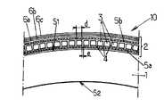
- FIG. 1is a plan view of an ophthalmic lens according to the invention.
- FIG. 2is a sectional view of a lens as per FIG. 1 ;
- FIG. 3illustrates a pair of spectacles provided with lenses according to FIGS. 1 and 2 .
- a spectacle lens blank 10also called an ophthalmic lens blank, comprises a substrate 1 having a convex anterior surface S 1 and a concave posterior surface S 2 .
- the substrate 1may itself be an ophthalmic lens blank as currently used at the present time. It may be made of an organic, mineral or composite material. It may also itself possess an optical function, such as an ophthalmic correction, a solar protection function, a photochromic function, etc.
- such a blank 10is intended to be machined along an outline denoted by C so as to form a lens that can then be fitted into the frame of a pair of spectacles.
- One of the surfaces S 1 or S 2 of the lens 10may include an array of cells 3 that are juxtaposed, one beside another, parallel to this surface, so as to form a paving of the surface.
- This pavingmay have any pattern: square, triangular, hexagonal or random.
- FIG. 1a partial cut-away shows a square paving formed by the cells 3 , given as an example.
- the cells 3are separated by walls approximately perpendicular to the surface S 1 .
- the dimension d of the cells 3 measured parallel to the surface S 1 and the thickness e of the walls 4are selected in such a way that the total area occupied by the cells 3 corresponds to a high coverage ratio of the lens 10 .
- This coverage ratioalso called the fill factor, is preferably greater than 95%, or even greater than 98%. In this way, the function conferred by the cells 3 on the lens 10 has a high effectiveness.
- the dimension d of the cells and the thickness e of the wallsare also selected so as not to cause light scattering or diffraction, which would be irksome to the person wearing the lens, or would be unattractive.
- the dimension dis preferably greater than 1 ⁇ m.
- this dimensionis advantageously less than 500 ⁇ m, so that each cell 3 cannot be individually distinguished by the naked eye.
- the lens 10thus meets the aesthetic criteria usually adopted in the ophthalmic field.
- the dimension d of the cellsis between 5 ⁇ m and 200 ⁇ m
- the thickness e of the walls 4is generally between 0.1 ⁇ m and 5 ⁇ m, and advantageously between 1 ⁇ m and 3 ⁇ m.
- the depth of the cellsis preferably between 1 ⁇ m and 50 ⁇ m. In one particular exemplary embodiment, it is equal to 10 ⁇ m.
- Such systemsare for example described in Patent Application WO 2006/013250.
- Electrodesare placed on either side of the array of cells 3 , parallel to the surface S 1 .
- the electrodes 5 a and 5 bhave outlines that are preferably superposed on and located close to the peripheral edge of the lens blank 10 .
- the electrodes 5 a and 5 bmake it possible to create a substantially uniform electric field across the cells when said electrodes are powered by an electrical voltage supply. This electric field is oriented perpendicular to the electrodes 5 a and 5 b.
- the array of cells 3is made of transparent or absorbent materials using techniques well known to those skilled in the art, such as that described for example in Patent Applications WO 2006/013250 or FR 05/07722.
- the electrodes 5 a , 5 bare advantageously made of transparent conducting materials such as a conducting oxide material like indium-doped tin oxide or ITO, or a conducting polymer, for example polyaniline, polyacetylene, or PEDOT.
- the electrodes 5 a , 5 bmay also each be formed from thin metal layers, such as silver layers. They are then advantageously combined with other layers of appropriate thickness and refractive index, in order to have a sufficient level of transparency.
- quarter-wave layerswhich represent one particular embodiment of the invention.
- the array of cells 3 and the electrodes 5 a , 5 bare advantageously designed to be cut at the same time as the substrate 1 during the operation of machining it.
- the electrode 5 a , the array of cells 3 and the electrode 5 bmay be formed in succession on the surface S 1 of the substrate 1 .
- additional treatmentsmay be applied on top of the electrode 5 b , in order to impart improved characteristics on the final lens.
- Such treatmentsknown to those skilled in the art, may consist in forming one of the following layers, or a combination thereof: an impact-resistant layer 6 a , an antireflection multilayer 6 b and an anti-fouling layer 6 c .
- Other additional treatmentsmay also be applied to the lens after formation of the electrode 5 b.
- a plastic filmadvantageously consisting of poly(para-xylylene) (or parylene) is deposited conformally between the electrode 5 b and the array of cells 3 filled with one or more electroactive materials.
- the paryleneis deposited by evaporating a parylene dimer at 150° C. Pyrolysing at 680° C. produces a gaseous reactive monomer that is vacuum-deposited, which, by polymerizing, thus forms a continuous insulation film both on the walls 4 of the cells and on the electro-active materials filling each of the cells.
- the electrode 5 bis then formed on said continuous, homogeneous and uniformly thick film made of parylene.
- the electrode 5 a , the array of cells 3 , the electrode 5 b and optionally the layers 6 a - 6 c , together with the parylene filmmay form a thin two-dimensional structure on a flexible transparent film support, which is attached to the surface S 1 of the substrate 1 .
- a structurereferenced 2 in FIG. 2 , can then be manufactured independently of the substrate 1 and then machined and bonded to one of the faces of said substrate, according to the requirements of a person intended to wear the lens 10 .
- the overall thin two-dimensional structure on the flexible supportforms a transparent functional film.
- the optical componentmust in particular have characteristics allowing it to be bonded to a curved surface, such as that formed by an optical lens or an ophthalmic lens.
- the optical componentmust thus comprise materials, especially at the electrodes, which are capable of undergoing deformation, be it minimal, by a thermoforming process, the latter being particularly suitable for integrating the transparent optical component into an ophthalmic lens.
- a person skilled in the artmay in particular refer to Patent FR 05/03306 describing such a process for applying a plane surface to a curved surface.
- the cells 3which are located between the electrodes 5 a and 5 b , are hermetically sealed so that each permanently contains an electroactive material.
- electroactive materialsare liquids, or possibly gels, they may be simply introduced into the cells 3 before they are closed off, for example using a printing head, especially of the material jet type.
- a printing headespecially of the material jet type.
- Such a headcomprises several liquid projection orifices, which may be supplied respectively by reservoirs of different liquid electroactive materials. It is therefore easy, by programming the positioning of the printing head in front of the array of cells 3 and by activating the liquid projection by one of the orifices, to fill the cells 3 with different materials depending on the position of each cell on the surface S 1 .
- the cells 3may be closed off by a continuous film that is sealed or bonded onto the tops of the walls 4 .
- the electrode 5 bis then supported by this film.
- the optical componentcomprises cells containing non-electroactive materials, these are also liquids or possibly gels. Thus, these cells may be filled by the same material jet device as that used previously.
- the electroactive materials that are contained in the cells 3may consist of at least two material components that are common to these cells and are mixed in each cell 3 in mixture proportions that vary according to the cell.
- the two material componentsare liquids, it is then sufficient for the printing head to have two orifices connected to two feed reservoirs for each of the components.
- the desired proportions of each component in each cell 3may then be obtained by suitably controlling the amount of each component that is projected into the cell by the printing head.
- the mixtures constituting the electroactive materials contained in at least certain of the cells 3comprise at least one liquid crystal.
- the proportion of this liquid crystal in the mixturesvaries among certain of the cells 3 so as to confer thereon different variations in an optical refractive index in response to the application of an electrical voltage between the electrodes 5 a and 5 b .
- the optical characteristic of each cell, which is modified upon applying the voltage,is therefore the apparent optical refractive index of the material contained in the cells.
- the refractive index gradients, which are oriented parallel to the surface S 1may thus be temporarily and reversibly generated by means of an electrical control.
- these gradientswhich are initially determined by the variations in the composition of the electroactive materials contained in the cells 3 , form a phase grating or spatial light modulator (SLM). They may correspond to different optical functions. Examples of such functions have already been mentioned above. A person skilled in the art knows the gradient profile that it is necessary to generate in order to obtain a particular optical function.
- the electroactive material contained in at least one of the cells 3has an optical refractive index variation of greater than 0.02, preferably between 0.02 and 0.2 or even possibly greater than 0.2, in response to the electrical signal applied between the two electrodes. In this way, the optical function of the electrically controllable lens 10 may have a sufficient amplitude.
- This optical functionmay be switched between two predefined fixed states in a binary fashion.
- a continuous variation of the optical functionmay be controlled, between two extreme states, by means of an appropriate progressive electrical control.
- FIG. 3shows a pair of spectacles 100 that incorporates two lenses 10 as described above.
- the spectacles 100comprise a frame with two sides 11 , into which frame the lenses 10 are fitted. It furthermore includes at least one electrical signal source 12 and electrical connections 13 which connect each of the lenses 10 to a source 12 .
- Each source 12may be a cell or battery of appropriate dimensions.
- Two connections 13are needed to deliver the electrical signal to each of the lenses 10 . These two connections are connected to the electrodes 5 a and 5 b of the lens, respectively. To do this, each connection 13 may be equipped with a terminal suitable for coming into contact with one of the electrodes 5 a , 5 b of the lens when the latter is fitted into the frame.
- a control device 14may be placed on one or more of the connections 13 in order to allow the electrical signal to be transmitted between the source 12 and at least one of the lenses 10 .
- the control device 14may be a manual control device or an automatic control device depending on a signal delivered by a detector incorporated into the spectacles.
- FIG. 3shows a pair of spectacles 100 in which each lens 10 is supplied by an independent electrical circuit.
- This circuitcomprises, for each lens, an electrical voltage source 12 , two supply connections 13 and a switch 14 that are carried by the side 11 of the frame located on the same side as the lens.
- other electrical circuitsmay alternatively be used, comprising for example a single electrical voltage source 12 and a single switch 14 to deliver the same electrical signal to both lenses 10 . These are then connected so as to simultaneously activate the optical function of the two lenses 10 which is conferred by the electroactive materials thereof.
- the electrical components 12 - 14may also be provided on the frame, and possibly on the lenses 10 , in a different manner from that shown in FIG. 3 .
- the electrical signal source 12 dedicated to one of the two lenses 10may be integrated into the lens itself instead of being carried by the frame.
- the inventionmay be carried out in many alternative ways as regards each optical component, or a pair of spectacles equipped with such components, beyond the particular embodiments that have been mentioned or described in detail above.
Landscapes
- Physics & Mathematics (AREA)
- Ophthalmology & Optometry (AREA)
- General Physics & Mathematics (AREA)
- Optics & Photonics (AREA)
- Health & Medical Sciences (AREA)
- Nonlinear Science (AREA)
- General Health & Medical Sciences (AREA)
- Mathematical Physics (AREA)
- Chemical & Material Sciences (AREA)
- Crystallography & Structural Chemistry (AREA)
- Electrochromic Elements, Electrophoresis, Or Variable Reflection Or Absorption Elements (AREA)
- Liquid Crystal (AREA)
- Eyeglasses (AREA)
- Polarising Elements (AREA)
Abstract
Description
- a transparent array of hermetically sealed cells juxtaposed parallel to one surface of the component; and
- two transparent electrodes parallel to the surface of the component and lying opposite each other in a direction normal to the surface of the component.
n=(ns×nv)
n×e=λ/4
where n is the refractive index at 25° C. for a wavelength λ=550 nm of the quarter-wave plate (the wavelength corresponding to the eye's maximum sensitivity), nsis the refractive index at 25° C. for a wavelength λ=550 nm of the substrate of the optical component and nvis the refractive index at 25° C. for a wavelength λ=550 nm of the electrode directly in contact with the quarter-wave plate.
- producing a variable wavefront deformation for light passing through the component; the electrical signal applied to the electrodes enables the retardation function of the phase plate to be modified, thereby introducing a deformation of the wavefront;
- conferring a variable prismatic power;
- forming a variable holographic grating;
- when the component is an optical lens, reversibly modifying an optical power of the lens;
- variably correcting at least one optical aberration of the lens, such as for example a geometric aberration or a chromatic aberration; and
- when the component is a progressive ophthalmic lens intended to be fitted into the frame of a pair of spectacles, also called a PAL (progressive addition lens), variably modifying a design of this lens.
Claims (35)
Applications Claiming Priority (3)
| Application Number | Priority Date | Filing Date | Title |
|---|---|---|---|
| FR0609183AFR2907559B1 (en) | 2006-10-19 | 2006-10-19 | ELECRO-COMMANDABLE OPTICAL COMPONENT COMPRISING A SET OF CELLS |
| FR0609183 | 2006-10-19 | ||
| PCT/EP2007/061090WO2008046858A1 (en) | 2006-10-19 | 2007-10-17 | Electrically controllable optical component comprising an array of cells |
Publications (2)
| Publication Number | Publication Date |
|---|---|
| US20110013136A1 US20110013136A1 (en) | 2011-01-20 |
| US8801177B2true US8801177B2 (en) | 2014-08-12 |
Family
ID=37998455
Family Applications (1)
| Application Number | Title | Priority Date | Filing Date |
|---|---|---|---|
| US12/446,370Expired - Fee RelatedUS8801177B2 (en) | 2006-10-19 | 2007-10-17 | Electrically controllable optical component comprising an array of cells |
Country Status (5)
| Country | Link |
|---|---|
| US (1) | US8801177B2 (en) |
| EP (1) | EP2082285A1 (en) |
| JP (1) | JP5341766B2 (en) |
| FR (1) | FR2907559B1 (en) |
| WO (1) | WO2008046858A1 (en) |
Cited By (10)
| Publication number | Priority date | Publication date | Assignee | Title |
|---|---|---|---|---|
| US20160116775A1 (en)* | 2014-10-28 | 2016-04-28 | Samsung Display Co., Ltd. | Liquid crystal display device and manufacturing method thereof |
| US9897886B2 (en) | 2015-02-10 | 2018-02-20 | LAFORGE Optical, Inc. | Lens for displaying a virtual image |
| US11529230B2 (en) | 2019-04-05 | 2022-12-20 | Amo Groningen B.V. | Systems and methods for correcting power of an intraocular lens using refractive index writing |
| US11564839B2 (en) | 2019-04-05 | 2023-01-31 | Amo Groningen B.V. | Systems and methods for vergence matching of an intraocular lens with refractive index writing |
| US11583388B2 (en) | 2019-04-05 | 2023-02-21 | Amo Groningen B.V. | Systems and methods for spectacle independence using refractive index writing with an intraocular lens |
| US11583389B2 (en) | 2019-04-05 | 2023-02-21 | Amo Groningen B.V. | Systems and methods for correcting photic phenomenon from an intraocular lens and using refractive index writing |
| US11678975B2 (en) | 2019-04-05 | 2023-06-20 | Amo Groningen B.V. | Systems and methods for treating ocular disease with an intraocular lens and refractive index writing |
| US11944574B2 (en) | 2019-04-05 | 2024-04-02 | Amo Groningen B.V. | Systems and methods for multiple layer intraocular lens and using refractive index writing |
| US12357509B2 (en) | 2019-04-05 | 2025-07-15 | Amo Groningen B.V. | Systems and methods for improving vision from an intraocular lens in an incorrect position and using refractive index writing |
| US12377622B2 (en) | 2019-04-05 | 2025-08-05 | Amo Groningen B.V. | Systems and methods for vergence matching with an optical profile and using refractive index writing |
Families Citing this family (25)
| Publication number | Priority date | Publication date | Assignee | Title |
|---|---|---|---|---|
| FR2910642B1 (en)* | 2006-12-26 | 2009-03-06 | Essilor Int | TRANSPARENT OPTICAL COMPONENT WITH TWO CELL ARRAYS |
| US8801174B2 (en) | 2011-02-11 | 2014-08-12 | Hpo Assets Llc | Electronic frames comprising electrical conductors |
| US8944590B2 (en) | 2010-07-02 | 2015-02-03 | Mitsui Chemicals, Inc. | Electronic spectacle frames |
| US20120002160A1 (en) | 2010-07-02 | 2012-01-05 | Pixel Optics, Inc. | Frame design for electronic spectacles |
| US10613355B2 (en)* | 2007-05-04 | 2020-04-07 | E-Vision, Llc | Moisture-resistant eye wear |
| US8979259B2 (en) | 2010-07-02 | 2015-03-17 | Mitsui Chemicals, Inc. | Electro-active spectacle frames |
| US8905541B2 (en) | 2010-07-02 | 2014-12-09 | Mitsui Chemicals, Inc. | Electronic spectacle frames |
| US11061252B2 (en) | 2007-05-04 | 2021-07-13 | E-Vision, Llc | Hinge for electronic spectacles |
| US8523354B2 (en)* | 2008-04-11 | 2013-09-03 | Pixeloptics Inc. | Electro-active diffractive lens and method for making the same |
| FR2939916B1 (en)* | 2008-12-15 | 2011-04-01 | Essilor Int | OPTICAL ELEMENT WITH VARIABLE POWER |
| FR2939910B1 (en)* | 2008-12-15 | 2011-04-01 | Essilor Int | TRANSPARENT OPTICAL ELEMENT COMPRISING A SET OF CELLS |
| JP5729878B2 (en) | 2009-01-09 | 2015-06-03 | 三井化学株式会社 | Electroactive glasses and related electronic equipment |
| FR2960305B1 (en)* | 2010-05-21 | 2013-03-01 | Essilor Int | IMPLEMENTING A TRANSPARENT OPTICAL COMPONENT WITH A CELLULAR STRUCTURE |
| US12436411B2 (en) | 2010-07-02 | 2025-10-07 | E-Vision Optics, Llc | Moisture-resistant eye wear |
| JP5721042B2 (en) | 2010-10-20 | 2015-05-20 | 株式会社ニコン | Microscope system |
| JP5757458B2 (en) | 2011-04-12 | 2015-07-29 | 株式会社ニコン | Microscope system, server and program |
| WO2013025933A1 (en) | 2011-08-17 | 2013-02-21 | Pixeloptics, Inc. | Moisture-resistant electronic spectacle frames |
| JP5761458B2 (en) | 2012-06-05 | 2015-08-12 | 株式会社ニコン | Microscope equipment |
| US9389433B2 (en)* | 2013-03-15 | 2016-07-12 | Johnson Johnson Vision Care, Inc. | Methods and apparatus to form ophthalmic devices incorporating photonic elements |
| US9429769B2 (en)* | 2013-05-09 | 2016-08-30 | Johnson & Johnson Vision Care, Inc. | Ophthalmic device with thin film nanocrystal integrated circuits |
| FR3008196B1 (en)* | 2013-07-08 | 2016-12-30 | Essilor Int | METHOD FOR MANUFACTURING AT LEAST ONE OPHTHALMIC LENS |
| ES2576489T3 (en)* | 2013-08-02 | 2016-07-07 | Essilor International (Compagnie Générale d'Optique) | A method to control a programmable ophthalmic lens device |
| TWI546666B (en)* | 2014-11-03 | 2016-08-21 | 慧榮科技股份有限公司 | Data storage device and flash memory control method |
| CN108803124B (en)* | 2018-06-27 | 2021-05-28 | 武汉华星光电技术有限公司 | Curved liquid crystal display screen and manufacturing method thereof |
| CN115390273A (en)* | 2022-09-30 | 2022-11-25 | 维沃移动通信有限公司 | Spectacles and focusing method thereof |
Citations (108)
| Publication number | Priority date | Publication date | Assignee | Title |
|---|---|---|---|---|
| US2196066A (en) | 1938-03-02 | 1940-04-02 | Feinbloom William | Contact lens |
| US2511329A (en) | 1946-12-26 | 1950-06-13 | Craig Edward | Lens shield |
| US3460960A (en) | 1965-05-03 | 1969-08-12 | Owens Illinois Inc | Coated glass and method of making same |
| US3532038A (en) | 1967-06-05 | 1970-10-06 | Ibm | Multi-lens devices for the fabrication of semiconductor devices |
| US3628854A (en) | 1969-12-08 | 1971-12-21 | Optical Sciences Group Inc | Flexible fresnel refracting membrane adhered to ophthalmic lens |
| US3978580A (en) | 1973-06-28 | 1976-09-07 | Hughes Aircraft Company | Method of fabricating a liquid crystal display |
| US4150878A (en) | 1974-04-05 | 1979-04-24 | Giorgio Barzilai | Hollow-space cell and method for its manufacture |
| US4268132A (en) | 1979-09-24 | 1981-05-19 | Neefe Charles W | Oxygen generating contact lens |
| US4601545A (en) | 1984-05-16 | 1986-07-22 | Kern Seymour P | Variable power lens system |
| US4621912A (en) | 1985-02-14 | 1986-11-11 | Meyer Donald R | Foraminated optical contact lens |
| US4720173A (en) | 1984-03-09 | 1988-01-19 | Canon Kabushiki Kaisha | Display having an orientation treatment between 0° and 15° to the spacer wall |
| US4791417A (en) | 1983-03-01 | 1988-12-13 | Tadeusz Bobak | Display device |
| US4994664A (en) | 1989-03-27 | 1991-02-19 | Massachusetts Institute Of Technology | Optically coupled focal plane arrays using lenslets and multiplexers |
| US5017000A (en) | 1986-05-14 | 1991-05-21 | Cohen Allen L | Multifocals using phase shifting |
| US5044742A (en) | 1988-03-24 | 1991-09-03 | Amir Cohen | Contact lens |
| US5067795A (en) | 1986-03-24 | 1991-11-26 | Gianni Bulgari S.P.A. | Adjustable transparency spectacles |
| US5139707A (en) | 1989-06-05 | 1992-08-18 | Essilor International (Compagnie Generale D'optique) | Indolino-spiroquinoxalino oxazine photochromatic compounds, methods for their preparation, photochromic compositions and articles containing such compounds |
| US5233038A (en) | 1990-12-06 | 1993-08-03 | Essilor International (Compagnie Generale D'optique) | Photochronic compounds of the indolino-spiro-benzoxazine type |
| US5359444A (en) | 1992-12-24 | 1994-10-25 | Motorola, Inc. | Auto-focusing optical apparatus |
| FR2718447B1 (en) | 1994-04-06 | 1996-05-24 | Essilor Int | Chromenes of the 2,2-diphenyl type heteroannelated in 6.7 and their use in the field of ophthalmic optics. |
| US5529725A (en) | 1993-11-17 | 1996-06-25 | Essilor International | Spirooxazines and use thereof in the field of ophthalmic optics |
| EP0728572A2 (en) | 1995-02-27 | 1996-08-28 | Essilor International Compagnie Generale D'optique | Process for making transparent articles of graduated refractive index |
| US5576870A (en) | 1993-04-23 | 1996-11-19 | Matsushita Electric Industrial Co., Ltd. | Liquid crystal display panel having a phase grating formed of liquid crystal molecules |
| US5585968A (en) | 1993-12-01 | 1996-12-17 | International Business Machines Corporation | Optical elements having regions of different indices of refraction and method of fabricating the same |
| US5604280A (en) | 1994-04-06 | 1997-02-18 | Essilor International Compagnie Generale D'optique | Ring spiro [fluorene-[2H]-benzopyranes] and their use in ophthalmic optics |
| US5699142A (en) | 1994-09-01 | 1997-12-16 | Alcon Laboratories, Inc. | Diffractive multifocal ophthalmic lens |
| US5733077A (en) | 1996-07-02 | 1998-03-31 | The Hilsinger Company Lp | Lens drill guide |
| US5764333A (en) | 1997-02-27 | 1998-06-09 | Somsel; John R. | Sunshields for eyeglasses |
| US5763054A (en) | 1996-09-13 | 1998-06-09 | Trw Inc. | Anti-reflection treatment for optical elements |
| US5774273A (en) | 1996-08-23 | 1998-06-30 | Vari-Lite, Inc. | Variable-geometry liquid-filled lens apparatus and method for controlling the energy distribution of a light beam |
| US5805263A (en) | 1995-10-20 | 1998-09-08 | Christian Dalloz S.A. | Lens blanks, process of manufacture therefor and eyewear incorporating lenses made therefrom |
| US5812235A (en) | 1996-09-04 | 1998-09-22 | Pemrable Technologies Inc. | Multifocal corneal contact lenses |
| DE19714434A1 (en) | 1997-04-08 | 1998-10-15 | Armin Schaeuble | Selective electronic photo-protective spectacles |
| US5905561A (en) | 1996-06-14 | 1999-05-18 | Pbh, Inc. | Annular mask lens having diffraction reducing edges |
| US5914802A (en) | 1997-07-18 | 1999-06-22 | Northrop Grumman Corporation | Combined spatial light modulator and phase mask for holographic storage system |
| US6019914A (en) | 1997-05-06 | 2000-02-01 | Essilor International Compagnie Generale D'optique | Photochromic spirooxazine compounds, their use in the field of ophthalmic optics |
| US6091546A (en)* | 1997-10-30 | 2000-07-18 | The Microoptical Corporation | Eyeglass interface system |
| US6118510A (en) | 1996-07-26 | 2000-09-12 | Sharp Kabushiki Kaisha | Liquid crystal device |
| CA2340672A1 (en) | 1999-06-16 | 2000-12-21 | Creavis Gesellschaft Fur Technologie Und Innovation Mbh | Electrically switchable composite films |
| US6199986B1 (en) | 1999-10-21 | 2001-03-13 | University Of Rochester | Rapid, automatic measurement of the eye's wave aberration |
| US6259501B1 (en) | 1998-11-27 | 2001-07-10 | Zvi Yaniv | Liquid crystal display with dielectric layer having at least two openings corresponding to each picture element and method of making same |
| US6274288B1 (en) | 1995-06-12 | 2001-08-14 | California Institute Of Technology | Self-trapping and self-focusing of optical beams in photopolymers |
| US6281366B1 (en) | 2000-02-29 | 2001-08-28 | Essilor International Compagnie Generale D'optique | Photochromic [3H]naphtho[2,1-b]pyran compounds containing an acetylenic substituent, process for their manufacture, and photochromic materials and articles obtained |
| US6301051B1 (en) | 2000-04-05 | 2001-10-09 | Rockwell Technologies, Llc | High fill-factor microlens array and fabrication method |
| US6307243B1 (en) | 1999-07-19 | 2001-10-23 | Micron Technology, Inc. | Microlens array with improved fill factor |
| US6309803B1 (en) | 1999-07-01 | 2001-10-30 | Lumenon, Innovative Lightwave Technology, Inc. | On-substrate cleaving of sol-gel waveguide |
| US6327072B1 (en) | 1999-04-06 | 2001-12-04 | E Ink Corporation | Microcell electrophoretic displays |
| US20020008898A1 (en) | 2000-05-30 | 2002-01-24 | Seiko Epson Corporation | Electrophoretic display and method for producing same |
| US20020016629A1 (en) | 2000-03-20 | 2002-02-07 | Sandstedt Christian A. | Application of wavefront sensor to lenses capable of post-fabrication power modification |
| US20020080464A1 (en) | 2000-11-27 | 2002-06-27 | Bruns Donald G. | Wavefront aberrator and method of manufacturing |
| US20020114054A1 (en) | 2001-02-19 | 2002-08-22 | Koninklijke Philips Electronics N.V. | Optical element and method of manufacturing such an optical element |
| US6449099B2 (en) | 2000-03-23 | 2002-09-10 | Rohm Co., Ltd. | Lens array and lens array assembly |
| US20020140899A1 (en) | 2000-06-23 | 2002-10-03 | Blum Ronald D. | Electro-optic lens with integrated components |
| US20020145797A1 (en) | 2001-02-07 | 2002-10-10 | Sales Tasso R.M. | High-contrast screen with random microlens array |
| US20020167638A1 (en) | 2001-05-10 | 2002-11-14 | Young-Sang Byun | Method of forming a liquid crystal layer using an ink jet system |
| US6485599B1 (en) | 2000-07-11 | 2002-11-26 | International Business Machines Corporation | Curing of sealants using multiple frequencies of radiation |
| US20020176963A1 (en) | 2001-04-23 | 2002-11-28 | Sipix Imaging, Inc. | Microcup compositions having improved flexure resistance and release properties |
| US20030003295A1 (en) | 2000-11-27 | 2003-01-02 | Dreher Andreas W. | Apparatus and method of correcting higher-order aberrations of the human eye |
| US20030021005A1 (en) | 2001-07-27 | 2003-01-30 | Rong-Chang Liang | Electrophoretic display with color filters |
| JP2003504665A (en) | 1999-07-02 | 2003-02-04 | イー・ビジョン・エルエルシー | System, apparatus and method for correcting vision using an electro-active lens |
| US20030035199A1 (en) | 2001-08-20 | 2003-02-20 | Rong-Chang Liang | Transflective electrophoretic display |
| US20030081172A1 (en) | 2001-10-25 | 2003-05-01 | Dreher Andreas W. | Eyeglass manufacturing method using variable index layer |
| US20030085906A1 (en) | 2001-05-09 | 2003-05-08 | Clairvoyante Laboratories, Inc. | Methods and systems for sub-pixel rendering with adaptive filtering |
| US6577434B2 (en) | 2000-01-14 | 2003-06-10 | Minolta Co., Ltd. | Variable focal position spatial modulation device |
| US6597340B1 (en) | 1999-03-05 | 2003-07-22 | Seiko Epson Corporation | Electrophoresis display and its production method |
| US20030143391A1 (en) | 2001-06-04 | 2003-07-31 | Lai Shui T. | Apparatus and method of fabricating a compensating element for wavefront correction using spatially localized curing of resin mixtures |
| US20030147046A1 (en) | 2002-02-06 | 2003-08-07 | Shadduck John H. | Adaptive optic lens system and method of use |
| US20030152849A1 (en) | 2001-02-15 | 2003-08-14 | Mary Chan-Park | Process for roll-to-roll manufacture of a display by synchronized photolithographic exposure on a substrate web |
| US20030174385A1 (en) | 2001-06-11 | 2003-09-18 | Rong-Chang Liang | Process for manufacture of improved color displays |
| US20030206260A1 (en) | 1999-07-16 | 2003-11-06 | Minolta Co., Ltd | Liquid crystal display and method to manufacture the same |
| US20040008319A1 (en) | 2002-07-11 | 2004-01-15 | Lai Shui T. | Optical elements and methods for making thereof |
| US20040027327A1 (en) | 2002-06-10 | 2004-02-12 | E Ink Corporation | Components and methods for use in electro-optic displays |
| US6707516B1 (en) | 1995-05-23 | 2004-03-16 | Colorlink, Inc. | Single-panel field-sequential color display systems |
| US20040051833A1 (en) | 2001-01-12 | 2004-03-18 | Mathias Hain | Optical compensation element |
| US20040114111A1 (en) | 2002-01-23 | 2004-06-17 | Shinya Watanabe | Image display and image projector |
| WO2004051354A1 (en) | 2002-12-04 | 2004-06-17 | Sipix Imaging, Inc. | Multilayer display and manufacturing method using sealant composition |
| US20040120667A1 (en) | 2002-12-23 | 2004-06-24 | Eastman Kodak Company | Walled network optical component |
| US20040125247A1 (en) | 2002-12-26 | 2004-07-01 | Krishna Seshan | Method for fabricating microelectronic image projection devices |
| US20040125337A1 (en) | 2002-10-04 | 2004-07-01 | Vision-Ease | Laminated functional wafer for plastic optical elements |
| US20040165252A1 (en) | 2000-03-03 | 2004-08-26 | Rong-Chang Liang | Electrophoretic display and novel process for its manufacture |
| US20040169932A1 (en) | 2002-11-20 | 2004-09-02 | Powervision | Lens system and methods for power adjustment |
| JP2004527785A (en) | 2002-01-08 | 2004-09-09 | トムソン ライセンシング ソシエテ アノニム | Optical compensator |
| US20040233381A1 (en) | 2001-08-07 | 2004-11-25 | Kim Hyoung Sik | Lens fixing apparatus for rimless spectacle |
| JP2005128518A (en) | 2003-10-02 | 2005-05-19 | Citizen Watch Co Ltd | Variable focus lens |
| WO2005033782A3 (en) | 2003-10-03 | 2005-07-21 | Invisia Ltd | Multifocal lens |
| US6963435B2 (en) | 2002-03-27 | 2005-11-08 | Avery Dennison Corporation | Switchable electro-optical laminates |
| US20060006336A1 (en) | 2004-07-02 | 2006-01-12 | Essilor International | Process for producing a transparent optical element, optical component involved in this process and optical element thus obtained |
| EP1308770B1 (en) | 2001-10-31 | 2006-04-26 | Optrex Corporation | Liquid crystal display element |
| US20060087614A1 (en) | 2002-08-12 | 2006-04-27 | Shadduck John H | Adaptive optic lens system and method of use |
| US7036929B1 (en) | 2004-04-12 | 2006-05-02 | William Rolf Harvey | Method and device for the application and removal of disposable corrective optical film to an eyeglass lens |
| WO2006067309A1 (en) | 2004-12-17 | 2006-06-29 | Essilor International (Compagnie Generale D'optique) | Method for making a transparent optical element, optical component used in said method and resulting optical element |
| EP1225458B1 (en) | 2001-01-19 | 2006-07-26 | Centre National De La Recherche Scientifique (Cnrs) | Method for the manufacturing of a multilayer guided-wave device on a substrate, and guided-wave device obtained therewith |
| FR2872589B1 (en) | 2004-07-02 | 2006-10-27 | Essilor Int | METHOD FOR PRODUCING A TRANSPARENT OPTICAL ELEMENT, OPTICAL COMPONENT INVOLVED IN THIS METHOD AND OPTICAL ELEMENT THUS OBTAINED |
| US7144529B1 (en) | 1999-06-22 | 2006-12-05 | Essilor International | Method for molding ophthalmic lenses |
| US20060279848A1 (en) | 2003-07-14 | 2006-12-14 | Koninklijke Philips Electronics N. V. | Variable lens |
| WO2006050366A3 (en) | 2004-11-02 | 2006-12-14 | E Vision Llc | Electro-active spectacles and method of fabricating same |
| WO2007010414A3 (en) | 2005-07-20 | 2007-03-29 | Essilor Int | Randomly pixellated optical component, its fabrication method and its use in the fabrication of a transparent optical element |
| WO2007023383A3 (en) | 2005-07-20 | 2007-05-03 | Essilor Int | Optical component with cells |
| US7227692B2 (en) | 2003-10-09 | 2007-06-05 | Micron Technology, Inc | Method and apparatus for balancing color response of imagers |
| US20070152560A1 (en) | 2004-01-21 | 2007-07-05 | Dai Nippon Printing Co., Ltd. | Display front panel, and method for producing the same |
| WO2007144308A1 (en) | 2006-06-13 | 2007-12-21 | Essilor International (Compagnie Generale D'optique) | Method of bonding a film to a curved substrate |
| US20080068723A1 (en) | 2004-09-07 | 2008-03-20 | Ophthonix, Inc. | Monomers and polymers for optical elements |
| US7404637B2 (en) | 1999-03-01 | 2008-07-29 | Boston Innovative Optics, Inc. | System and method for increasing the depth of focus of the human eye |
| US20080208335A1 (en)* | 2007-01-22 | 2008-08-28 | Blum Ronald D | Flexible electro-active lens |
| US20080212018A1 (en) | 2005-07-20 | 2008-09-04 | Essilor International | Transparent Pixelized Optical Component with Absorbing Walls, its Method of Manufacture and its Use in the Manufacture of a Transparent Optical Element |
| US20080314499A1 (en) | 2005-04-04 | 2008-12-25 | Essilor International (Compagnie General D'optique | Apparatus for Conforming a Planar Film on an Optical Lens, Method for Functionalizing an Optical Lens By Means of Said Apparatus, the Optical Lens So-Obtained |
| US7533453B2 (en) | 2005-01-24 | 2009-05-19 | Yancy Virgil T | E-facet optical lens |
| US7715107B2 (en) | 2006-04-25 | 2010-05-11 | Asml Netherlands B.V. | Optical element for correction of aberration, and a lithographic apparatus comprising same |
Family Cites Families (6)
| Publication number | Priority date | Publication date | Assignee | Title |
|---|---|---|---|---|
| JPS61140920A (en)* | 1984-12-13 | 1986-06-28 | Olympus Optical Co Ltd | Liquid crystal lens |
| JPS61177428A (en)* | 1985-02-01 | 1986-08-09 | Olympus Optical Co Ltd | Spectacles of liquid crystal |
| JPH0527214A (en)* | 1991-07-23 | 1993-02-05 | Toyota Motor Corp | Variable focal length liquid crystal lens |
| US6005651A (en)* | 1992-08-04 | 1999-12-21 | Matsushita Electric Industrial Co., Ltd. | Display panel and projection display system with use of display panel |
| JP3331559B2 (en)* | 1997-11-13 | 2002-10-07 | 日本電信電話株式会社 | Optical device |
| JPH11352453A (en)* | 1998-06-09 | 1999-12-24 | Olympus Optical Co Ltd | Optical characteristic variable optical element |
- 2006
- 2006-10-19FRFR0609183Apatent/FR2907559B1/ennot_activeExpired - Fee Related
- 2007
- 2007-10-17JPJP2009532795Apatent/JP5341766B2/ennot_activeExpired - Fee Related
- 2007-10-17USUS12/446,370patent/US8801177B2/ennot_activeExpired - Fee Related
- 2007-10-17WOPCT/EP2007/061090patent/WO2008046858A1/enactiveApplication Filing
- 2007-10-17EPEP07821455Apatent/EP2082285A1/ennot_activeWithdrawn
Patent Citations (118)
| Publication number | Priority date | Publication date | Assignee | Title |
|---|---|---|---|---|
| US2196066A (en) | 1938-03-02 | 1940-04-02 | Feinbloom William | Contact lens |
| US2511329A (en) | 1946-12-26 | 1950-06-13 | Craig Edward | Lens shield |
| US3460960A (en) | 1965-05-03 | 1969-08-12 | Owens Illinois Inc | Coated glass and method of making same |
| US3532038A (en) | 1967-06-05 | 1970-10-06 | Ibm | Multi-lens devices for the fabrication of semiconductor devices |
| US3628854A (en) | 1969-12-08 | 1971-12-21 | Optical Sciences Group Inc | Flexible fresnel refracting membrane adhered to ophthalmic lens |
| US3978580A (en) | 1973-06-28 | 1976-09-07 | Hughes Aircraft Company | Method of fabricating a liquid crystal display |
| US4150878A (en) | 1974-04-05 | 1979-04-24 | Giorgio Barzilai | Hollow-space cell and method for its manufacture |
| US4268132A (en) | 1979-09-24 | 1981-05-19 | Neefe Charles W | Oxygen generating contact lens |
| US4791417A (en) | 1983-03-01 | 1988-12-13 | Tadeusz Bobak | Display device |
| US4720173A (en) | 1984-03-09 | 1988-01-19 | Canon Kabushiki Kaisha | Display having an orientation treatment between 0° and 15° to the spacer wall |
| FR2561005B1 (en) | 1984-03-09 | 1990-04-20 | Canon Kk | OPTICAL MODULATION DEVICE |
| US4601545A (en) | 1984-05-16 | 1986-07-22 | Kern Seymour P | Variable power lens system |
| US4621912A (en) | 1985-02-14 | 1986-11-11 | Meyer Donald R | Foraminated optical contact lens |
| US5067795A (en) | 1986-03-24 | 1991-11-26 | Gianni Bulgari S.P.A. | Adjustable transparency spectacles |
| US5017000A (en) | 1986-05-14 | 1991-05-21 | Cohen Allen L | Multifocals using phase shifting |
| US5044742A (en) | 1988-03-24 | 1991-09-03 | Amir Cohen | Contact lens |
| US4994664A (en) | 1989-03-27 | 1991-02-19 | Massachusetts Institute Of Technology | Optically coupled focal plane arrays using lenslets and multiplexers |
| US5139707A (en) | 1989-06-05 | 1992-08-18 | Essilor International (Compagnie Generale D'optique) | Indolino-spiroquinoxalino oxazine photochromatic compounds, methods for their preparation, photochromic compositions and articles containing such compounds |
| US5233038A (en) | 1990-12-06 | 1993-08-03 | Essilor International (Compagnie Generale D'optique) | Photochronic compounds of the indolino-spiro-benzoxazine type |
| US5359444A (en) | 1992-12-24 | 1994-10-25 | Motorola, Inc. | Auto-focusing optical apparatus |
| US5576870A (en) | 1993-04-23 | 1996-11-19 | Matsushita Electric Industrial Co., Ltd. | Liquid crystal display panel having a phase grating formed of liquid crystal molecules |
| US5529725A (en) | 1993-11-17 | 1996-06-25 | Essilor International | Spirooxazines and use thereof in the field of ophthalmic optics |
| US5585968A (en) | 1993-12-01 | 1996-12-17 | International Business Machines Corporation | Optical elements having regions of different indices of refraction and method of fabricating the same |
| FR2718447B1 (en) | 1994-04-06 | 1996-05-24 | Essilor Int | Chromenes of the 2,2-diphenyl type heteroannelated in 6.7 and their use in the field of ophthalmic optics. |
| US5604280A (en) | 1994-04-06 | 1997-02-18 | Essilor International Compagnie Generale D'optique | Ring spiro [fluorene-[2H]-benzopyranes] and their use in ophthalmic optics |
| US5699142A (en) | 1994-09-01 | 1997-12-16 | Alcon Laboratories, Inc. | Diffractive multifocal ophthalmic lens |
| EP0728572A2 (en) | 1995-02-27 | 1996-08-28 | Essilor International Compagnie Generale D'optique | Process for making transparent articles of graduated refractive index |
| US5807906A (en) | 1995-02-27 | 1998-09-15 | Essilor International-Compagnie Generale D'optique | Process for obtaining a transparent article with a refractive index gradient |
| US6707516B1 (en) | 1995-05-23 | 2004-03-16 | Colorlink, Inc. | Single-panel field-sequential color display systems |
| US6274288B1 (en) | 1995-06-12 | 2001-08-14 | California Institute Of Technology | Self-trapping and self-focusing of optical beams in photopolymers |
| US5805263A (en) | 1995-10-20 | 1998-09-08 | Christian Dalloz S.A. | Lens blanks, process of manufacture therefor and eyewear incorporating lenses made therefrom |
| US5905561A (en) | 1996-06-14 | 1999-05-18 | Pbh, Inc. | Annular mask lens having diffraction reducing edges |
| US5733077A (en) | 1996-07-02 | 1998-03-31 | The Hilsinger Company Lp | Lens drill guide |
| US6118510A (en) | 1996-07-26 | 2000-09-12 | Sharp Kabushiki Kaisha | Liquid crystal device |
| US5774273A (en) | 1996-08-23 | 1998-06-30 | Vari-Lite, Inc. | Variable-geometry liquid-filled lens apparatus and method for controlling the energy distribution of a light beam |
| US5812235A (en) | 1996-09-04 | 1998-09-22 | Pemrable Technologies Inc. | Multifocal corneal contact lenses |
| US5763054A (en) | 1996-09-13 | 1998-06-09 | Trw Inc. | Anti-reflection treatment for optical elements |
| US5764333A (en) | 1997-02-27 | 1998-06-09 | Somsel; John R. | Sunshields for eyeglasses |
| DE19714434A1 (en) | 1997-04-08 | 1998-10-15 | Armin Schaeuble | Selective electronic photo-protective spectacles |
| US6019914A (en) | 1997-05-06 | 2000-02-01 | Essilor International Compagnie Generale D'optique | Photochromic spirooxazine compounds, their use in the field of ophthalmic optics |
| US5914802A (en) | 1997-07-18 | 1999-06-22 | Northrop Grumman Corporation | Combined spatial light modulator and phase mask for holographic storage system |
| US6091546A (en)* | 1997-10-30 | 2000-07-18 | The Microoptical Corporation | Eyeglass interface system |
| US6259501B1 (en) | 1998-11-27 | 2001-07-10 | Zvi Yaniv | Liquid crystal display with dielectric layer having at least two openings corresponding to each picture element and method of making same |
| US7404637B2 (en) | 1999-03-01 | 2008-07-29 | Boston Innovative Optics, Inc. | System and method for increasing the depth of focus of the human eye |
| US6597340B1 (en) | 1999-03-05 | 2003-07-22 | Seiko Epson Corporation | Electrophoresis display and its production method |
| US6327072B1 (en) | 1999-04-06 | 2001-12-04 | E Ink Corporation | Microcell electrophoretic displays |
| CA2340672A1 (en) | 1999-06-16 | 2000-12-21 | Creavis Gesellschaft Fur Technologie Und Innovation Mbh | Electrically switchable composite films |
| US7144529B1 (en) | 1999-06-22 | 2006-12-05 | Essilor International | Method for molding ophthalmic lenses |
| US6309803B1 (en) | 1999-07-01 | 2001-10-30 | Lumenon, Innovative Lightwave Technology, Inc. | On-substrate cleaving of sol-gel waveguide |
| JP2003504665A (en) | 1999-07-02 | 2003-02-04 | イー・ビジョン・エルエルシー | System, apparatus and method for correcting vision using an electro-active lens |
| US20030206260A1 (en) | 1999-07-16 | 2003-11-06 | Minolta Co., Ltd | Liquid crystal display and method to manufacture the same |
| US6307243B1 (en) | 1999-07-19 | 2001-10-23 | Micron Technology, Inc. | Microlens array with improved fill factor |
| US6199986B1 (en) | 1999-10-21 | 2001-03-13 | University Of Rochester | Rapid, automatic measurement of the eye's wave aberration |
| US6577434B2 (en) | 2000-01-14 | 2003-06-10 | Minolta Co., Ltd. | Variable focal position spatial modulation device |
| US6281366B1 (en) | 2000-02-29 | 2001-08-28 | Essilor International Compagnie Generale D'optique | Photochromic [3H]naphtho[2,1-b]pyran compounds containing an acetylenic substituent, process for their manufacture, and photochromic materials and articles obtained |
| US20040165252A1 (en) | 2000-03-03 | 2004-08-26 | Rong-Chang Liang | Electrophoretic display and novel process for its manufacture |
| US6987605B2 (en) | 2000-03-03 | 2006-01-17 | Sipix Imaging, Inc. | Transflective electrophoretic display |
| US20040190115A1 (en) | 2000-03-03 | 2004-09-30 | Rong-Chang Liang | Transflective electrophoretic display |
| US20020016629A1 (en) | 2000-03-20 | 2002-02-07 | Sandstedt Christian A. | Application of wavefront sensor to lenses capable of post-fabrication power modification |
| US6449099B2 (en) | 2000-03-23 | 2002-09-10 | Rohm Co., Ltd. | Lens array and lens array assembly |
| US6301051B1 (en) | 2000-04-05 | 2001-10-09 | Rockwell Technologies, Llc | High fill-factor microlens array and fabrication method |
| US20020008898A1 (en) | 2000-05-30 | 2002-01-24 | Seiko Epson Corporation | Electrophoretic display and method for producing same |
| US6871951B2 (en)* | 2000-06-23 | 2005-03-29 | E-Vision, Llc | Electro-optic lens with integrated components |
| US20020140899A1 (en) | 2000-06-23 | 2002-10-03 | Blum Ronald D. | Electro-optic lens with integrated components |
| US6485599B1 (en) | 2000-07-11 | 2002-11-26 | International Business Machines Corporation | Curing of sealants using multiple frequencies of radiation |
| US20030003295A1 (en) | 2000-11-27 | 2003-01-02 | Dreher Andreas W. | Apparatus and method of correcting higher-order aberrations of the human eye |
| US20020080464A1 (en) | 2000-11-27 | 2002-06-27 | Bruns Donald G. | Wavefront aberrator and method of manufacturing |
| US20040051833A1 (en) | 2001-01-12 | 2004-03-18 | Mathias Hain | Optical compensation element |
| EP1225458B1 (en) | 2001-01-19 | 2006-07-26 | Centre National De La Recherche Scientifique (Cnrs) | Method for the manufacturing of a multilayer guided-wave device on a substrate, and guided-wave device obtained therewith |
| US20020145797A1 (en) | 2001-02-07 | 2002-10-10 | Sales Tasso R.M. | High-contrast screen with random microlens array |
| US20030152849A1 (en) | 2001-02-15 | 2003-08-14 | Mary Chan-Park | Process for roll-to-roll manufacture of a display by synchronized photolithographic exposure on a substrate web |
| US20020114054A1 (en) | 2001-02-19 | 2002-08-22 | Koninklijke Philips Electronics N.V. | Optical element and method of manufacturing such an optical element |
| US20020176963A1 (en) | 2001-04-23 | 2002-11-28 | Sipix Imaging, Inc. | Microcup compositions having improved flexure resistance and release properties |
| US20030085906A1 (en) | 2001-05-09 | 2003-05-08 | Clairvoyante Laboratories, Inc. | Methods and systems for sub-pixel rendering with adaptive filtering |
| US20020167638A1 (en) | 2001-05-10 | 2002-11-14 | Young-Sang Byun | Method of forming a liquid crystal layer using an ink jet system |
| US20030143391A1 (en) | 2001-06-04 | 2003-07-31 | Lai Shui T. | Apparatus and method of fabricating a compensating element for wavefront correction using spatially localized curing of resin mixtures |
| US20030174385A1 (en) | 2001-06-11 | 2003-09-18 | Rong-Chang Liang | Process for manufacture of improved color displays |
| US20030021005A1 (en) | 2001-07-27 | 2003-01-30 | Rong-Chang Liang | Electrophoretic display with color filters |
| US20040233381A1 (en) | 2001-08-07 | 2004-11-25 | Kim Hyoung Sik | Lens fixing apparatus for rimless spectacle |
| US20030035199A1 (en) | 2001-08-20 | 2003-02-20 | Rong-Chang Liang | Transflective electrophoretic display |
| US20030081172A1 (en) | 2001-10-25 | 2003-05-01 | Dreher Andreas W. | Eyeglass manufacturing method using variable index layer |
| US6712466B2 (en) | 2001-10-25 | 2004-03-30 | Ophthonix, Inc. | Eyeglass manufacturing method using variable index layer |
| EP1308770B1 (en) | 2001-10-31 | 2006-04-26 | Optrex Corporation | Liquid crystal display element |
| JP2004527785A (en) | 2002-01-08 | 2004-09-09 | トムソン ライセンシング ソシエテ アノニム | Optical compensator |
| US20040114111A1 (en) | 2002-01-23 | 2004-06-17 | Shinya Watanabe | Image display and image projector |
| US20030147046A1 (en) | 2002-02-06 | 2003-08-07 | Shadduck John H. | Adaptive optic lens system and method of use |
| US6963435B2 (en) | 2002-03-27 | 2005-11-08 | Avery Dennison Corporation | Switchable electro-optical laminates |
| US20040027327A1 (en) | 2002-06-10 | 2004-02-12 | E Ink Corporation | Components and methods for use in electro-optic displays |
| US20040008319A1 (en) | 2002-07-11 | 2004-01-15 | Lai Shui T. | Optical elements and methods for making thereof |
| US6934088B2 (en) | 2002-07-11 | 2005-08-23 | Ophthonix, Inc. | Optical elements and methods for making thereof |
| US20060087614A1 (en) | 2002-08-12 | 2006-04-27 | Shadduck John H | Adaptive optic lens system and method of use |
| WO2004015481A1 (en) | 2002-08-12 | 2004-02-19 | Ophthonix, Inc. | Apparatus and method of correcting higher-order aberrations of the human eye |
| WO2004034095A2 (en) | 2002-10-03 | 2004-04-22 | Ophthonix, Inc. | Apparatus and method of fabricating a compensating element for wavefront correction using spatially localized curing of resin mixtures |
| US20040125337A1 (en) | 2002-10-04 | 2004-07-01 | Vision-Ease | Laminated functional wafer for plastic optical elements |
| US20040169932A1 (en) | 2002-11-20 | 2004-09-02 | Powervision | Lens system and methods for power adjustment |
| WO2004051354A1 (en) | 2002-12-04 | 2004-06-17 | Sipix Imaging, Inc. | Multilayer display and manufacturing method using sealant composition |
| US20040120667A1 (en) | 2002-12-23 | 2004-06-24 | Eastman Kodak Company | Walled network optical component |
| US20040125247A1 (en) | 2002-12-26 | 2004-07-01 | Krishna Seshan | Method for fabricating microelectronic image projection devices |
| US20060279848A1 (en) | 2003-07-14 | 2006-12-14 | Koninklijke Philips Electronics N. V. | Variable lens |
| JP2005128518A (en) | 2003-10-02 | 2005-05-19 | Citizen Watch Co Ltd | Variable focus lens |
| WO2005033782A3 (en) | 2003-10-03 | 2005-07-21 | Invisia Ltd | Multifocal lens |
| US7289260B2 (en) | 2003-10-03 | 2007-10-30 | Invisia Ltd. | Multifocal lens |
| US7227692B2 (en) | 2003-10-09 | 2007-06-05 | Micron Technology, Inc | Method and apparatus for balancing color response of imagers |
| US20070152560A1 (en) | 2004-01-21 | 2007-07-05 | Dai Nippon Printing Co., Ltd. | Display front panel, and method for producing the same |
| US7036929B1 (en) | 2004-04-12 | 2006-05-02 | William Rolf Harvey | Method and device for the application and removal of disposable corrective optical film to an eyeglass lens |
| FR2872589B1 (en) | 2004-07-02 | 2006-10-27 | Essilor Int | METHOD FOR PRODUCING A TRANSPARENT OPTICAL ELEMENT, OPTICAL COMPONENT INVOLVED IN THIS METHOD AND OPTICAL ELEMENT THUS OBTAINED |
| US20060006336A1 (en) | 2004-07-02 | 2006-01-12 | Essilor International | Process for producing a transparent optical element, optical component involved in this process and optical element thus obtained |
| US20080068723A1 (en) | 2004-09-07 | 2008-03-20 | Ophthonix, Inc. | Monomers and polymers for optical elements |
| WO2006050366A3 (en) | 2004-11-02 | 2006-12-14 | E Vision Llc | Electro-active spectacles and method of fabricating same |
| WO2006067309A1 (en) | 2004-12-17 | 2006-06-29 | Essilor International (Compagnie Generale D'optique) | Method for making a transparent optical element, optical component used in said method and resulting optical element |
| US7533453B2 (en) | 2005-01-24 | 2009-05-19 | Yancy Virgil T | E-facet optical lens |
| US20080314499A1 (en) | 2005-04-04 | 2008-12-25 | Essilor International (Compagnie General D'optique | Apparatus for Conforming a Planar Film on an Optical Lens, Method for Functionalizing an Optical Lens By Means of Said Apparatus, the Optical Lens So-Obtained |
| WO2007023383A3 (en) | 2005-07-20 | 2007-05-03 | Essilor Int | Optical component with cells |
| WO2007010414A3 (en) | 2005-07-20 | 2007-03-29 | Essilor Int | Randomly pixellated optical component, its fabrication method and its use in the fabrication of a transparent optical element |
| US20080212018A1 (en) | 2005-07-20 | 2008-09-04 | Essilor International | Transparent Pixelized Optical Component with Absorbing Walls, its Method of Manufacture and its Use in the Manufacture of a Transparent Optical Element |
| US7715107B2 (en) | 2006-04-25 | 2010-05-11 | Asml Netherlands B.V. | Optical element for correction of aberration, and a lithographic apparatus comprising same |
| WO2007144308A1 (en) | 2006-06-13 | 2007-12-21 | Essilor International (Compagnie Generale D'optique) | Method of bonding a film to a curved substrate |
| US20080208335A1 (en)* | 2007-01-22 | 2008-08-28 | Blum Ronald D | Flexible electro-active lens |
Non-Patent Citations (6)
| Title |
|---|
| Cognard, Philippe. "Colles et adhesifs pour emballages, Generalities," 18 pages (English Summary Provided). |
| David R. Lide, ed., CRC Handbook of Chemistry and Physics, 89th edition (internet version 2009), CRC Press/Taylor and Francis, Boca Raton, FL., pp. 10-12 through 10-13. |
| Fowles, Grant R. Introduction to Modern Optics. New York: Dover Publications, 1989. Print. pp. 138-139. |
| Hecht, Eugene, "Optics, 4th Edition" 2002 Addison Wesley, p. 428 (XP002465206). |
| Kaufman U.S. Appl. No. 60/507,940 Drawing Sheets 4, 5. |
| Perez, Jose-Philippe, (Optique-Fondement et applications [Optics-Fundamentals and Applications], 7th edition, Paris 2004, p. 262) (English summary provided). |
Cited By (13)
| Publication number | Priority date | Publication date | Assignee | Title |
|---|---|---|---|---|
| US20160116775A1 (en)* | 2014-10-28 | 2016-04-28 | Samsung Display Co., Ltd. | Liquid crystal display device and manufacturing method thereof |
| US9897886B2 (en) | 2015-02-10 | 2018-02-20 | LAFORGE Optical, Inc. | Lens for displaying a virtual image |
| US11529230B2 (en) | 2019-04-05 | 2022-12-20 | Amo Groningen B.V. | Systems and methods for correcting power of an intraocular lens using refractive index writing |
| US11564839B2 (en) | 2019-04-05 | 2023-01-31 | Amo Groningen B.V. | Systems and methods for vergence matching of an intraocular lens with refractive index writing |
| US11583388B2 (en) | 2019-04-05 | 2023-02-21 | Amo Groningen B.V. | Systems and methods for spectacle independence using refractive index writing with an intraocular lens |
| US11583389B2 (en) | 2019-04-05 | 2023-02-21 | Amo Groningen B.V. | Systems and methods for correcting photic phenomenon from an intraocular lens and using refractive index writing |
| US11678975B2 (en) | 2019-04-05 | 2023-06-20 | Amo Groningen B.V. | Systems and methods for treating ocular disease with an intraocular lens and refractive index writing |
| US11931296B2 (en) | 2019-04-05 | 2024-03-19 | Amo Groningen B.V. | Systems and methods for vergence matching of an intraocular lens with refractive index writing |
| US11944574B2 (en) | 2019-04-05 | 2024-04-02 | Amo Groningen B.V. | Systems and methods for multiple layer intraocular lens and using refractive index writing |
| US12357509B2 (en) | 2019-04-05 | 2025-07-15 | Amo Groningen B.V. | Systems and methods for improving vision from an intraocular lens in an incorrect position and using refractive index writing |
| US12357449B2 (en) | 2019-04-05 | 2025-07-15 | Amo Groningen B.V. | Systems and methods for treating ocular disease with an intraocular lens and refractive index writing |
| US12377622B2 (en) | 2019-04-05 | 2025-08-05 | Amo Groningen B.V. | Systems and methods for vergence matching with an optical profile and using refractive index writing |
| US12409028B2 (en) | 2019-04-05 | 2025-09-09 | Amo Groningen B.V. | Systems and methods for correcting photic phenomenon from an intraocular lens and using refractive index writing |
Also Published As
| Publication number | Publication date |
|---|---|
| US20110013136A1 (en) | 2011-01-20 |
| EP2082285A1 (en) | 2009-07-29 |
| FR2907559A1 (en) | 2008-04-25 |
| WO2008046858A1 (en) | 2008-04-24 |
| FR2907559B1 (en) | 2009-02-13 |
| JP2010507119A (en) | 2010-03-04 |
| JP5341766B2 (en) | 2013-11-13 |
Similar Documents
| Publication | Publication Date | Title |
|---|---|---|
| US8801177B2 (en) | Electrically controllable optical component comprising an array of cells | |
| US6927894B2 (en) | Mirror assemblies incorporating variable index of refraction materials | |
| US7019890B2 (en) | Hybrid electro-active lens | |
| US8587734B2 (en) | Adaptive lens for vision correction | |
| JP2005505789A (en) | Hybrid electroactive lens | |
| US9001282B2 (en) | Variable power optical element | |
| JP2007334348A (en) | Optical element and display, reflector, and backlight including the same | |
| US20120307165A1 (en) | Imaging System | |
| US20220252931A1 (en) | Gradient-index liquid crystal device with masked electrode boundary | |
| EP3701322B1 (en) | Spectacle lens comprising an activable optical filter and optical equipment comprising such spectacle lens | |
| TW200525184A (en) | Improved hybrid electro-active lens | |
| US11953777B2 (en) | Display module and display device | |
| JP3900189B2 (en) | Liquid crystal display device and method of manufacturing liquid crystal display device | |
| JP3931904B2 (en) | Method for manufacturing liquid crystal display device and liquid crystal display device | |
| CN120406026A (en) | concave lens | |
| JP2007114791A (en) | Liquid crystal display | |
| EP3737992A1 (en) | Tunable fresnel lens with improved image quality | |
| AU2002341982A1 (en) | Hybrid electro-active lens | |
| AU2008240326A1 (en) | Hybrid electro-active lens |
Legal Events
| Date | Code | Title | Description |
|---|---|---|---|
| AS | Assignment | Owner name:ESSILOR INTERNATIONAL (COMPAGNIE GENERALE D'OPTIQU Free format text:ASSIGNMENT OF ASSIGNORS INTEREST;ASSIGNORS:ARCHAMBEAU, SAMUEL;CANO, JEAN-PAUL;BOVET, CHRISTIAN;SIGNING DATES FROM 20090710 TO 20090720;REEL/FRAME:023068/0593 | |
| AS | Assignment | Owner name:ESSILOR INTERNATIONAL (COMPAGNIE GENERALE D'OPTIQU Free format text:ASSIGNMENT OF ASSIGNORS INTEREST;ASSIGNORS:ARCHAMBEAU, SAMUEL;CANO, JEAN-PAUL;BOVET, CHRISTIAN;SIGNING DATES FROM 20090710 TO 20090720;REEL/FRAME:025004/0935 | |
| STCF | Information on status: patent grant | Free format text:PATENTED CASE | |
| MAFP | Maintenance fee payment | Free format text:PAYMENT OF MAINTENANCE FEE, 4TH YEAR, LARGE ENTITY (ORIGINAL EVENT CODE: M1551) Year of fee payment:4 | |
| AS | Assignment | Owner name:ESSILOR INTERNATIONAL, FRANCE Free format text:ASSIGNMENT OF ASSIGNORS INTEREST;ASSIGNOR:ESSILOR INTERNATIONAL (COMPAGNIE GENERALE D'OPTIQUE);REEL/FRAME:045853/0275 Effective date:20171101 | |
| FEPP | Fee payment procedure | Free format text:MAINTENANCE FEE REMINDER MAILED (ORIGINAL EVENT CODE: REM.); ENTITY STATUS OF PATENT OWNER: LARGE ENTITY | |
| LAPS | Lapse for failure to pay maintenance fees | Free format text:PATENT EXPIRED FOR FAILURE TO PAY MAINTENANCE FEES (ORIGINAL EVENT CODE: EXP.); ENTITY STATUS OF PATENT OWNER: LARGE ENTITY | |
| STCH | Information on status: patent discontinuation | Free format text:PATENT EXPIRED DUE TO NONPAYMENT OF MAINTENANCE FEES UNDER 37 CFR 1.362 | |
| FP | Lapsed due to failure to pay maintenance fee | Effective date:20220812 |