US8797279B2 - Analog touchscreen methods and apparatus - Google Patents
Analog touchscreen methods and apparatusDownload PDFInfo
- Publication number
- US8797279B2 US8797279B2US12/787,368US78736810AUS8797279B2US 8797279 B2US8797279 B2US 8797279B2US 78736810 AUS78736810 AUS 78736810AUS 8797279 B2US8797279 B2US 8797279B2
- Authority
- US
- United States
- Prior art keywords
- display
- region
- user
- physical
- computing device
- Prior art date
- Legal status (The legal status is an assumption and is not a legal conclusion. Google has not performed a legal analysis and makes no representation as to the accuracy of the status listed.)
- Active, expires
Links
Images


Classifications
- G—PHYSICS
- G06—COMPUTING OR CALCULATING; COUNTING
- G06F—ELECTRIC DIGITAL DATA PROCESSING
- G06F3/00—Input arrangements for transferring data to be processed into a form capable of being handled by the computer; Output arrangements for transferring data from processing unit to output unit, e.g. interface arrangements
- G06F3/01—Input arrangements or combined input and output arrangements for interaction between user and computer
- G06F3/03—Arrangements for converting the position or the displacement of a member into a coded form
- G06F3/041—Digitisers, e.g. for touch screens or touch pads, characterised by the transducing means
- G06F3/0416—Control or interface arrangements specially adapted for digitisers
- G—PHYSICS
- G06—COMPUTING OR CALCULATING; COUNTING
- G06F—ELECTRIC DIGITAL DATA PROCESSING
- G06F3/00—Input arrangements for transferring data to be processed into a form capable of being handled by the computer; Output arrangements for transferring data from processing unit to output unit, e.g. interface arrangements
- G06F3/01—Input arrangements or combined input and output arrangements for interaction between user and computer
- G06F3/048—Interaction techniques based on graphical user interfaces [GUI]
- G06F3/0487—Interaction techniques based on graphical user interfaces [GUI] using specific features provided by the input device, e.g. functions controlled by the rotation of a mouse with dual sensing arrangements, or of the nature of the input device, e.g. tap gestures based on pressure sensed by a digitiser
- G06F3/0488—Interaction techniques based on graphical user interfaces [GUI] using specific features provided by the input device, e.g. functions controlled by the rotation of a mouse with dual sensing arrangements, or of the nature of the input device, e.g. tap gestures based on pressure sensed by a digitiser using a touch-screen or digitiser, e.g. input of commands through traced gestures
- G06F3/04883—Interaction techniques based on graphical user interfaces [GUI] using specific features provided by the input device, e.g. functions controlled by the rotation of a mouse with dual sensing arrangements, or of the nature of the input device, e.g. tap gestures based on pressure sensed by a digitiser using a touch-screen or digitiser, e.g. input of commands through traced gestures for inputting data by handwriting, e.g. gesture or text
- G—PHYSICS
- G06—COMPUTING OR CALCULATING; COUNTING
- G06F—ELECTRIC DIGITAL DATA PROCESSING
- G06F2203/00—Indexing scheme relating to G06F3/00 - G06F3/048
- G06F2203/041—Indexing scheme relating to G06F3/041 - G06F3/045
- G06F2203/04105—Pressure sensors for measuring the pressure or force exerted on the touch surface without providing the touch position
- G—PHYSICS
- G06—COMPUTING OR CALCULATING; COUNTING
- G06F—ELECTRIC DIGITAL DATA PROCESSING
- G06F3/00—Input arrangements for transferring data to be processed into a form capable of being handled by the computer; Output arrangements for transferring data from processing unit to output unit, e.g. interface arrangements
- G06F3/01—Input arrangements or combined input and output arrangements for interaction between user and computer
- G06F3/03—Arrangements for converting the position or the displacement of a member into a coded form
- G06F3/041—Digitisers, e.g. for touch screens or touch pads, characterised by the transducing means
- G06F3/044—Digitisers, e.g. for touch screens or touch pads, characterised by the transducing means by capacitive means
- G—PHYSICS
- G06—COMPUTING OR CALCULATING; COUNTING
- G06F—ELECTRIC DIGITAL DATA PROCESSING
- G06F3/00—Input arrangements for transferring data to be processed into a form capable of being handled by the computer; Output arrangements for transferring data from processing unit to output unit, e.g. interface arrangements
- G06F3/01—Input arrangements or combined input and output arrangements for interaction between user and computer
- G06F3/03—Arrangements for converting the position or the displacement of a member into a coded form
- G06F3/041—Digitisers, e.g. for touch screens or touch pads, characterised by the transducing means
- G06F3/045—Digitisers, e.g. for touch screens or touch pads, characterised by the transducing means using resistive elements, e.g. a single continuous surface or two parallel surfaces put in contact
Definitions
- Embodiments of the present inventionrelate to touch screen devices. More specifically, the present invention relates to touch screen devices capable of sensing the force of a touch and methods of use thereof.
- touch screen devices and touch user interfacesare now quite common place for consumers: from the signature machine in the checkout isle, to automatic teller machines at banks, to ticketing kiosks at airports, and the like.
- Touch screen capabilityis also now quite common in hand-held devices: from the Palm Pilot, to the Google Nexus One, to the Apple iPad, and the like.
- Touch capabilityhas typically been enabled for many touch screen devices through the incorporation and use of a resistive sensor network. These sensor networks can sense when a single finger of the user touches the display, or uses a stylus to touch the display.
- Drawbacks to touch screen devices incorporating resistive-based sensors determined by the inventorinclude that if a user inadvertently touches two locations on the touch screen at the same time, the location reported by the touch screen if often incorrect. As such devices typically only support detecting one finger at a time, for example, the reported touch location may be between the two fingers. Another drawback includes that the user has to press down with some force on the touch screen before the touch screen can detect the user touch.
- capacitive-based touch screen displaysare now more commonly used and address some of the short comings of a resistive-based sensor network.
- capacitive-based touch screenscan sense the individual locations of fingers when the user touch the display with more than one finger. Accordingly, these devices are often termed “multi-touch” displays.
- capacitive-based touch screensdo not require the user to press-down upon the touch screen before the finger is sensed.
- resistive and capacitive based touch screeninclude that the sensed touches are typically binary in nature, i.e. either the finger is not touching or the finger is touching. These types of devices cannot sense the force with which a user touches the touch screen display. From a user point of view, these touch screen devices also do not provide a user with any sensation of pressing a button or key, i.e. they provide no tactile feedback.
- One type of touch screen display used by Research In Motion (RIM) to provide the user with tactile feedbackwas used in the Blackberry Storm series of devices.
- RIMResearch In Motion
- one or more micro sensorswere placed under the capacitive-based touch screen display.
- the touch screen displaywould then deflect (by about a millimeter) and cause one of the micro sensors to physically click or switch. The physical click would thus provide the user with tactile confirmation of the button press.
- Drawbacks to such approaches determined by the inventorinclude that such devices were limited to the physical performance of the micro sensors. For example, a user could not type very quickly with such an approach because the user had to pause between key presses to wait until the micro sensors could fully reset before she could press the next key. Further, if the user placed two or more fingers on the touch screen at the same time she depressed the touch screen (activating the micro sensor(s)), it would be unclear which touch screen location or finger the user intended.
- Embodiments of the present inventionrelate to touch screen devices. More specifically, the present invention relates to touch screen devices capable of sensing the force of a touch and methods of use thereof.
- a computer systemsuch as a cell phone, internet access device, media player, or the like having a touch screen display and one or more physical sensors.
- the functionassociated with the touched location is determined.
- the functionmay be running of an application program, selection of a function within an application program, and the like.
- a type and/or magnitude of movementis determined by the one or more physical sensors also in response to the user touching the touch screen display. Based upon the type and/or magnitude of movement or combinations of movements, an input parameter or value may be determined for use by the selected function. Next, the function is initiated and given the input parameter or value.
- a computer systemsuch as a tablet computer, a smart phone, cell phone, or the like also having a touch screen display and one or more physical sensors.
- the function associated with the touched locationis again determined.
- the functionmay be running of an application program, selection of a function within an application program, and the like.
- a type and/or magnitude of movementis determined by the one or more physical sensors also in response to the user touching the touch screen display. The type and/or magnitude of movement is then compared to one or more thresholds for type and/or magnitude of movement. In various embodiments, if the threshold is not exceeded, the function is uninhibited.
- a computer implemented method for determining an intensity of user input to a computer system, performed by the computer system that is programmed to perform the methodincludes determining by a touchscreen display of the computer system, an indication of a position of a first user-controlled user input device relative to the touchscreen display of the computer system in response to a user-initiated change in state of the first user-controlled user input device relative to the computer system, wherein the user-initiated change in state is also associated with a magnitude of change.
- a processmay include determining by a physical sensor of the computer system, the magnitude of change in sensed physical properties by the physical sensor in response to the user-implemented change in state of the first user-controlled user input device relative to the computer system and determining by the computer system, a user selection of a function to perform in response to the indication of the position of the first user-controlled user input device.
- a methodmay include determining by the computer system, an input parameter associated with the function in response to the magnitude of change in sensed physical properties, and initiating performance by the computer system, of the function in response to the input parameter.
- a computing deviceconfigured to display images to a user and configured to sense a user touch on the touchscreen display and a touchscreen display controller coupled to the touchscreen display, wherein the touchscreen display controller is configured to determine a selected location on the touchscreen display in response to the user touch.
- One deviceincludes a physical sensor, wherein the physical sensor is configured to sense physical forces acting upon the physical sensor and configured to determine magnitudes of change in physical forces acting upon the physical sensor in response to the user touch.
- One systemincludes a processor coupled to the touchscreen display controller and to the physical sensor, wherein the processor is programmed to determine a user-selected function to perform in response to the selected location on the touchscreen display, and wherein the processor is programmed to initiate execution of the user-selected function in response to the magnitudes of change in physical forces.
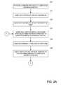
- FIG. 1illustrates a functional block diagram of various embodiments of the present invention.
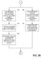
- FIGS. 2A-Dillustrate block diagrams of flow processes according to various embodiments of the present invention.
- FIG. 3is a simplified cross section diagram of components of a starting CMOS substrate according to one embodiment of the present invention.
- FIG. 4is a simplified cross section diagram of components of a monolithically integrated inertial sensing device according to one embodiment of the present invention.
- FIG. 5is a simplified cross section diagram of components of a monolithically integrated inertial sensing device according to one embodiment of the present invention.
- FIG. 6is a simplified cross section diagram of components of a monolithically integrated inertial sensing device according to one embodiment of the present invention.
- FIG. 7is a simplified cross section diagram of components of a monolithically integrated inertial sensing device according to one embodiment of the present invention.
- FIG. 8is a simplified cross section diagram of components of a monolithically integrated inertial sensing device according to one embodiment of the present invention.
- FIG. 9is a simplified cross section diagram of components of a monolithically integrated inertial sensing device according to one embodiment of the present invention.
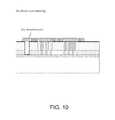
- FIG. 10is a simplified cross section diagram of components of a monolithically integrated inertial sensing device according to one embodiment of the present invention.
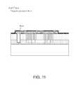
- FIG. 11is a simplified cross section diagram of components of a monolithically integrated inertial sensing device according to one embodiment of the present invention.
- FIG. 12is a simplified cross section diagram of components of a monolithically integrated inertial sensing device according to one embodiment of the present invention.
- FIG. 13is a simplified cross section diagram of components of a monolithically integrated inertial sensing device according to one embodiment of the present invention.
- FIG. 14is a simplified cross section diagram of components of a monolithically integrated inertial sensing device according to one embodiment of the present invention.
- FIGS. 15 , 16 , and 17are simplified cross section diagrams of double mechanical layer architecture of a monolithically integrated inertial sensing device according to one embodiment of the present invention.
- FIG. 1illustrates a functional block diagram of various embodiments of the present invention.
- a computing device 100typically includes an applications processor 110 , memory 120 , a touch screen display 130 and driver 140 , an image acquisition device 150 , audio input/output devices 160 , and the like. Additional communications from and to computing device are typically provided by via a wired interface 170 , a GPS/Wi-Fi/Bluetooth interface 180 , RF interfaces 190 and driver 200 , and the like. Also included in various embodiments are physical sensors 210 .
- computing device 100may be a hand-held computing device (e.g. Apple iPad, Apple iTouch, Dell Mini slate, Lenovo Skylight/IdeaPad, Asus EEE series, Microsoft Courier, Notion Ink Adam), a portable telephone (e.g. Apple iPhone, Motorola Droid, Google Nexus One, HTC Incredible/EVO 4G, Palm Pre series, Nokia N900), a portable computer (e.g. netbook, laptop), a media player (e.g. Microsoft Zune, Apple iPod), a reading device (e.g. Amazon Kindle, Barnes and Noble Nook), or the like.
- a hand-held computing devicee.g. Apple iPad, Apple iTouch, Dell Mini slate, Lenovo Skylight/IdeaPad, Asus EEE series, Microsoft Courier, Notion Ink Adam
- a portable telephonee.g. Apple iPhone, Motorola Droid, Google Nexus One, HTC Incredible/EVO 4G, Palm Pre series, Nokia N900
- a portable computere.g. netbook, laptop
- computing device 100may include one or more processors 110 .
- processors 110may also be termed application processors, and may include a processor core, a video/graphics core, and other cores.
- Processors 110may be a processor from Apple (A4), Intel (Atom), NVidia (Tegra 2), Marvell (Armada), Qualcomm (Snapdragon), Samsung, TI (OMAP), or the like.
- the processor coremay be an Intel processor, an ARM Holdings processor such as the Cortex-A, -M, -R or ARM series processors, or the like.
- the video/graphics coremay be an Imagination Technologies processor PowerVR-SGX, -MBX, -VGX graphics, an Nvidia graphics processor (e.g. GeForce), or the like.
- Other processing capabilitymay include audio processors, interface controllers, and the like. It is contemplated that other existing and/or later-developed processors may be used in various embodiments of the present invention.
- memory 120may include different types of memory (including memory controllers), such as flash memory (e.g. NOR, NAND), pseudo SRAM, DDR SDRAM, or the like.
- Memory 120may be fixed within computing device 100 or removable (e.g. SD, SDHC, MMC, MINI SD, MICRO SD, CF, SIM).
- computer-executable software codee.g. firmware, application programs
- application dataoperating system data or the like. It is contemplated that other existing and/or later-developed memory and memory technology may be used in various embodiments of the present invention.
- touch screen display 130 and driver 140may be based upon a variety of later-developed or current touch screen technology including resistive displays, capacitive displays, optical sensor displays, electromagnetic resonance, or the like. Additionally, touch screen display 130 may include single touch or multiple-touch sensing capability. Any later-developed or conventional output display technology may be used for the output display, such as TFT-LCD, OLED, Plasma, trans-reflective (Pixel Qi), electronic ink (e.g. electrophoretic, electrowetting, interferometric modulating). In various embodiments, the resolution of such displays and the resolution of such touch sensors may be set based upon engineering or non-engineering factors (e.g. sales, marketing). In some embodiments of the present invention, a display output port, such as an HDMI-based port or DVI-based port may also be included.
- a display output portsuch as an HDMI-based port or DVI-based port may also be included.
- image capture device 150may include a sensor, driver, lens and the like.
- the sensormay be based upon any later-developed or convention sensor technology, such as CMOS, CCD, or the like.
- image recognition software programsare provided to process the image data.
- such softwaremay provide functionality such as: facial recognition, head tracking, camera parameter control, or the like.
- audio input/output 160may include conventional microphone(s)/speakers. In some embodiments of the present invention, three-wire or four-wire audio connector ports are included to enable the user to use an external audio device such as external speakers, headphones or combination headphone/microphones.
- voice processing and/or recognition softwaremay be provided to applications processor 110 to enable the user to operate computing device 100 by stating voice commands. Additionally, a speech engine may be provided in various embodiments to enable computing device 100 to provide audio status messages, audio response messages, or the like.
- wired interface 170may be used to provide data transfers between computing device 100 and an external source, such as a computer, a remote server, a storage network, another computing device 100 , or the like.
- datamay include application data, operating system data, firmware, or the like.
- Embodimentsmay include any later-developed or conventional physical interface/protocol, such as: USB 2.0, 3.0, micro USB, mini USB, Firewire, Apple iPod connector, Ethernet, POTS, or the like. Additionally, software that enables communications over such networks is typically provided.
- a wireless interface 180may also be provided to provide wireless data transfers between computing device 100 and external sources, such as computers, storage networks, headphones, microphones, cameras, or the like.
- wireless protocolsmay include Wi-Fi (e.g. IEEE 802.11a/b/g/n, WiMax), Bluetooth, IR and the like.
- GPS receiving capabilitymay also be included in various embodiments of the present invention, however is not required. As illustrated in FIG. 1 , GPS functionality is included as part of wireless interface 180 merely for sake of convenience, although in implementation, such functionality is currently performed by circuitry that is distinct from the Wi-Fi circuitry and distinct from the Bluetooth circuitry.
- RF interfaces 190 and drivers 200may support any future-developed or conventional radio frequency communications protocol, such as CDMA-based protocols (e.g. WCDMA), GSM-based protocols, HSUPA-based protocols, or the like.
- driver 200is illustrated as being distinct from applications processor 110 . However, in some embodiments, these functionality are provided upon a single IC package, for example the Marvel PXA330 processor, and the like. It is contemplated that some embodiments of computing device 100 need not include the RF functionality provided by RF interface 190 and driver 200 .
- FIG. 1also illustrates computing device 100 to include physical sensors 210 .
- physical sensors 210are multi-axis Micro-Electro-Mechanical Systems (MEMS) based devices being developed by M-cube, the assignee of the present patent application.
- MEMSMicro-Electro-Mechanical Systems
- Physical sensors 210 developed by M-cubecurrently includes very low power three-axis sensors (linear, gyro or magnetic); ultra-low jitter three-axis sensors (linear, gyro or magnetic); low cost six-axis motion sensor (combination of linear, gyro, and/or magnetic); ten-axis sensors (linear, gyro, magnetic, pressure); and various combinations thereof.
- various embodiments of physical sensors 210are manufactured using a foundry-compatible process. As explained in such applications, because the process for manufacturing such physical sensors can be performed on a standard CMOS fabrication facility, it is expected that there will be a broader adoption of such components into computing device 100 .
- conventional physical sensors 210from Bosch, STMicroelectrnics, Analog Devices, Kionix or the like.
- any number of future developed or current operating systemsmay be supported, such as iPhone OS (e.g. 4.0), WindowsMobile (e.g. 7), Google Android (e.g. 2.1), Symbian, or the like.
- the operating systemmay be a multi-threaded multi-tasking operating system. Accordingly, inputs and/or outputs from and to touch screen display 130 and driver 140 and inputs/or outputs to physical sensors 210 may be processed in parallel processing threads. In other embodiments, such events or outputs may be processed serially, or the like. Inputs and outputs from other functional blocks may also be processed in parallel or serially, in other embodiments of the present invention, such as image acquisition device 150 and physical sensors 210 .
- FIG. 1is representative of one computing device 100 capable of embodying the present invention. It will be readily apparent to one of ordinary skill in the art that many other hardware and software configurations are suitable for use with the present invention. Embodiments of the present invention may include at least some but need not include all of the functional blocks illustrated in FIG. 1 .
- computing device 100may lack image acquisition unit 150 , or RF interface 190 and/or driver 200 , or GPS capability, or the like. Additional functions may also be added to various embodiments of computing device 100 , such as a physical keyboard, an additional image acquisition device, a trackball or trackpad, a joystick, or the like.
- multiple functional blocksmay be embodied into a single physical package or device, and various functional blocks may be divided and be performed among separate physical packages or devices.
- FIGS. 2A-Dillustrate block diagrams of flow processes according to various embodiments of the present invention.
- reference to elements in FIG. 1are provided in the discussion below merely for the sake of convenience.
- physical sensors 210are provided as part of a computing device 100 , step 300 .
- physical sensors 210 provided by the assignee of the present patent applicationare provided to an assembly entity to form computing device 100 .
- Computing device 100is then assembled, step 310 and provided for the user, step 320 .
- computing device 100may be a cell-phone, internet access device, a tablet computer, a personal media player/viewer, or the like running an appropriate operating system.
- computing device 100may display any number of graphical user interfaces including user-selectable regions on touch screen display 130 , step 320 .
- user-selectable regionsmay include radio buttons, sliders, selection buttons, text entry regions and the like.
- these soft buttonsmay be associated with application software functions, operating system functions, data management functions, telephony functions, audio processing functions, image processing functions, or the like.
- the userdetermines a function they wish computing device 100 to perform after viewing the graphical user interface, step 340 .
- the userthen touches or contacts a portion of touch screen display 130 corresponding to the user-selectable region, step 350 .
- the following processescan be performed in parallel by different processing threads, serially by one or more processes, or independently in separate processing threads.
- touch screen display 130senses the user contact in step 360 .
- touch screen display 130may perform this function via the use of resistive sensors, capacitive sensors, or the like.
- the user-selectable region within the GUIis determined, step 370 .
- computing device 100determines one or more functions associated with the user-selectable region, step 380 .
- computing device 100when a user contacts her finger on touch screen display 130 in step 350 , computing device 100 (physical sensors 210 ) will be physically perturbed, step 390 .
- computing device 100when the user touches touch screen display 130 , computing device 100 (physical sensors 210 ) will be subject to a force (e.g. a change in sensed physical state, a physical perturbation).
- this physical changecauses physical sensors 210 to sense a change in spatial location (sensed by an accelerometer), causes physical sensors 210 to sense a change its tilt or orientation (sensed by a gyroscope), or the like.
- FIG. 2Amerely references use of an accelerometer.
- this changecauses physical sensors 210 to sense a change in a magnetic field, sense a change in GPS coordinates, sense a change in temperature or air pressure, or the like.
- CMOS foundry-compatible MEMS physical sensor embodiments of the present inventionprovide a higher level of sensitivity and lower level of noise for such measurements than is currently available.
- the processmay then proceed to FIG. 2C or 2 D.
- the type of sensed perturbations and the thresholdmay be predetermined by the operating system, may be set by the user during, for example, a setup phase, may be specified by the application of function or the like.
- the thresholdmay be an acceleration in a ⁇ z-direction (away from a touch screen display) of 0.1 g, an acceleration in a ⁇ z-direction of 0.05 g followed by an acceleration in the +z-direction of 0.03 g; an acceleration of 0.1 g in the ⁇ z-direction and accelerations of 0.03 g in the x and y directions; a tilt of 0.5 degrees in a first axis rotation at the same time as a tilt of 1 degree in a second axis of rotation; a tilt of 0.2 degrees in a first axis followed by a tilt of ⁇ 0.3 degrees in the first axis; a increase in magnetic field by 10 gauss; an increase in atmospheric pressure of 10 mm Hg for 0.25 seconds; and the like.
- step 380if the threshold is exceeded, the function determined in step 380 is performed, step 420 ; if not, the process returns to step 330 .
- Embodimentsmay be applied to any number of different functions, for example, a virtual telephone keypad.
- a usermay inadvertently make a telephone call when the cell phone is in his pocket and he reaches for his keys. As his fingers brush against the virtual keypad, the telephone may interpret these as user selections for a telephone number to call.
- inadvertent callsmay be avoided if it is required that the physical sensors detect an acceleration (e.g. 0.1 g) primarily in the ⁇ z direction at about the same time the user touches the virtual keyboard keys.
- an acceleratione.g. 0.1 g
- the physical sensorsWhen in his pocket, when the fingers brush or knock against the key pad, the physical sensors may detect an acceleration of 0.05 g in the ⁇ z direction, 0.02 in the x direction and 0.05 in the y direction, then, the user touch may be ignored. Accordingly, the execution of unintended user functions on a computing device may be reduced.
- the process of FIG. 2Bmay proceed to FIG. 2D .
- a determinationis then made as to a value for an input parameter based upon the type, magnitude and/or direction of the sensed physical perturbations, step 430 .
- a relationship between the type of sensed perturbations and the input parametermay be predetermined by the operating system, may be set by the user during, for example, a setup phase, may be specified by the application of function or the like.
- an acceleration in a ⁇ z-direction (away from a touch screen display) of 0.1 gmay map to an input value of “1,” 0.2 g may map to “2,” 0.3 g may map to “3,” or the like; an acceleration in only a ⁇ z direction of 0.01 g may map to an input value of “256,” an acceleration of 0.01 g in the ⁇ z direction and 0.05 g in the x-direction may map to an input value of “512;” a clockwise roll of 0.1 degrees may map to an input value of “increase,” a counter clock-wise roll of 0.1 degrees may map to an input value of “decrease,” or the like.
- the functionmay be performed using this value.
- Embodimentsmay be applied to any number of different functions, for example, a painting program. In such cases, a harder tap may be associated with a larger paint spot upon a canvas, a softer tap may be associated with a smaller spot upon a canvas, and the like.
- other types of parametersmay also be adjusted based upon sensed physical change such as: position of graphic elements, brightness, contrast, gamma, sharpness, saturation, filter, and the like.
- a flick of a finger at a first velocity with a low impactmay be associated moving a series of images at a slower rate
- a flick of a finger at the first velocity with a higher impactmay be associated moving a series of images at a faster rate.
- other types of parametersmay also be adjusted, such as: rate of acceleration, rate of rotation, rate of zoom, rate of pan, and the like.
- the type or magnitude of sensed physical changemay control a volume level, a microphone sensitivity level, a bass level, a treble level, or the like. Accordingly, the execution of user functions may have different input parameters of values based upon sensed physical changes.
- FIG. 3is a simplified cross section diagram of components of a starting CMOS substrate according to one embodiment of the present invention.
- the starting substrateis a fully processed CMOS wafer.
- a dielectric layersuch as oxide and nitride is deposited on top of a top metal layer of the CMOS wafer.
- the dielectric layeris then patterned to form a structure that provides anchor points for stationary members of the mechanical sensing device.
- FIG. 4is a simplified cross section diagram of components of a monolithically integrated inertial sensing device according to one embodiment of the present invention.
- a silicon waferis bonded to the CMOS substrate.
- the bonding methodsinclude but not limited to: covalent, Sprin-on-glass (SOG), Eutectic, and anodic.
- SOGSprin-on-glass
- EutecticEutectic
- anodicThe bonding temperature is CMOS compatible and below 400C.
- FIG. 5is a simplified cross section diagram of components of a monolithically integrated inertial sensing device according to one embodiment of the present invention.
- the silicon substrateis thinned by techniques such as grinding, polishing, and etching.
- the final thickness of the remaining silicon atop of the CMOSis precisely measured by infrared interferometry method with nano meter accuracy. Infrared wavelength is used because silicon is transparent in this spectrum.
- FIG. 6is a simplified cross section diagram of components of a monolithically integrated inertial sensing device according to one embodiment of the present invention.
- a VIA holeis etched into the silicon and top dielectric layers and stop on the top metal layer.
- the size of the VIAranges from 0.5 um to a few micro meters depending on the thickness of the silicon layer.
- the profile or sidewall of the VIAis tapered or slopped for better step coverage of subsequent metalization step.
- FIG. 7is a simplified cross section diagram of components of a monolithically integrated inertial sensing device according to one embodiment of the present invention.
- a metal layeris blanket deposited on the wafer covering the silicon surface as well as the VIA surface.
- CVD or PVD recipesare optimized to achieve good step coverage of the VIA as well as low stress of the metal film.
- the metal layeris a CVD TiN material that has excellent step coverage of the VIA.
- the thickness of the metalranges from a few hundreds of angstroms to a few micro meters depending the applications requirements.
- An optional electroplating stepcan be used to fill the entire VIA with metals such as Copper or Nickel.
- FIG. 8is a simplified cross section diagram of components of a monolithically integrated inertial sensing device according to one embodiment of the present invention.
- the silicon layeris patterned typically by a DRIE step.
- the mechanical structureincludes a proof mass connected with springs, movable comb fingers and stationary comb fingers that anchored to the top oxide.
- the springshave desired stiffness/compliance that allows the proof mass to move at certain external acceleration.
- the comb fingers moving along with the proof masscouples to stationary comb fingers capacitively. The movement causes a change in capacitance between the movable comb fingers and stationary comb fingers.
- the capacitance changeis detected by the integrated circuits a few micrometer below.
- FIG. 9is a simplified cross section diagram of components of a monolithically integrated inertial sensing device according to one embodiment of the present invention.
- an organic sacrificial materialis deposited covering the mechanical structure.
- the sacrificial materialis a liquid photo resist that is spin coated on the wafer and fill all the VIA holes and trenches.
- the sacrificial materialis a dry film photoresist that is deposited on the surface of the wafer and does not fill the holes and trenches.
- FIG. 10is a simplified cross section diagram of components of a monolithically integrated inertial sensing device according to one embodiment of the present invention. As depicted, the photo resist is patterned by an exposure and develop lithography process. The exposed areas are non-trench features such as proof mass and anchors.
- FIG. 11is a simplified cross section diagram of components of a monolithically integrated inertial sensing device according to one embodiment of the present invention.
- the 1 st layer of the encapsulationis deposited by a PVD process.
- the deposition recipeis optimized for non-conforming purpose, which has little step coverage of the sidewall of the exposed photoresist trenches.
- FIG. 12is a simplified cross section diagram of components of a monolithically integrated inertial sensing device according to one embodiment of the present invention.
- the sacrificial organic materialis then removed by a dry O2 plasma ashing step. The removal of the sacrificial material releases the sensor device and forms the 1 st shell of the encapsulation.
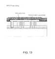
- FIG. 13is a simplified cross section diagram of components of a monolithically integrated inertial sensing device according to one embodiment of the present invention.
- the 2 nd layer of the encapsulationis deposited onto the 1 st layer.
- the sealing methodsinclude PVD, spin-on, or spray-on techniques.
- the sealing materialsinclude metal such as Ti, TiN, amorphous silicon, spin-on-glass, spray-on-glass, or a combination of the above.
- the ambient during sealingis optimized and controlled to a desired spec that defines the sensor device ambient after sealing.
- a getter materialsuch as Ti can be deposited as the 1 st layer of the encapsulation and activated later to achieve high vacuum and cleanness of the sensor ambient environment.
- an optional CVD dielectric materialsuch as oxide or nitride can be added onto the encapsulation.
- FIG. 14is a simplified cross section diagram of components of a monolithically integrated inertial sensing device according to one embodiment of the present invention. As shown, a bond pad structure is formed.
- the bond pad structurecan be formed by pattern and etch techniques known in the art, but can also be others depending on the application.
- the vertically monolithically integrated inertial sensorshave smaller chip size, lower parasitics, higher sensitivity, lower power, and lower cost.
- FIGS. 15 , 16 , and 17are simplified cross section diagrams of double mechanical layer architecture of a monolithically integrated inertial sensing device according to one embodiment of the present invention.
- piezoresistorsare embedded in the SOI substrate prior to bonding. After the bonding, a thinning process is followed to define a desired thickness of the remaining silicon in the bulk portion of the SOI substrate as illustrated in FIG. 16 .
- the thickness control techniquesinclude methods aforementioned, Infrared interferometry, VIA end-point, or double SOI substrate.
- the sensor structureis then defined by etching steps.
- the spring memberis formed in the SOI layer with the piezoresistors located in the mostly sensitive region. As the proof mass moves responding to an external acceleration, the springs deform accordingly. As a result, the strain generated in the springs change the resistance of the piezoresistors. The change in resistance is detected by the integrated circuits in a few micro below.
- the present inventioncan include a computing device including a processor coupled to a display, a display controller, and a physical sensor.
- the physical sensorcan include a monolithic MEMS and CMOS integrated circuit device.
- This integrated circuit devicecan include a first semiconductor substrate having a first surface region, one or more CMOS integrated circuit devices provided on a CMOS integrated circuit device region having a CMOS surface region overlying the first surface region, and a dielectric region having a cavity region therein overlying the CMOS surface region.
- the devicecan also include a second semiconductor substrate having a second surface region overlying the dielectric region and enclosing the cavity region.
- the second substratecan have a spring region overlying a vicinity of the cavity region.
- a first piezo resistor devicecan be provided within a first portion of the spring region of the second semiconductor substrate.
- a second piezo resistor devicecan be provided within a second portion of the spring region of the second semiconductor substrate.
- a mass of materialcan be coupled to a portion of the spring region of the second semiconductor substrate between the first and second piezo resistor devices. The mass of material can be configured overlying the cavity region and coupled to the spring region to be movable from at least a first position to a second position and to be sensed respectively by either or both the first and second piezo resistor devices.
Landscapes
- Engineering & Computer Science (AREA)
- General Engineering & Computer Science (AREA)
- Theoretical Computer Science (AREA)
- Human Computer Interaction (AREA)
- Physics & Mathematics (AREA)
- General Physics & Mathematics (AREA)
- Position Input By Displaying (AREA)
- User Interface Of Digital Computer (AREA)
Abstract
Description
Claims (8)
Priority Applications (3)
| Application Number | Priority Date | Filing Date | Title |
|---|---|---|---|
| US12/787,368US8797279B2 (en) | 2010-05-25 | 2010-05-25 | Analog touchscreen methods and apparatus |
| US12/940,026US8928602B1 (en) | 2009-03-03 | 2010-11-04 | Methods and apparatus for object tracking on a hand-held device |
| US13/069,355US8928696B1 (en) | 2010-05-25 | 2011-03-22 | Methods and apparatus for operating hysteresis on a hand held device |
Applications Claiming Priority (1)
| Application Number | Priority Date | Filing Date | Title |
|---|---|---|---|
| US12/787,368US8797279B2 (en) | 2010-05-25 | 2010-05-25 | Analog touchscreen methods and apparatus |
Publications (2)
| Publication Number | Publication Date |
|---|---|
| US20110291981A1 US20110291981A1 (en) | 2011-12-01 |
| US8797279B2true US8797279B2 (en) | 2014-08-05 |
Family
ID=45021691
Family Applications (1)
| Application Number | Title | Priority Date | Filing Date |
|---|---|---|---|
| US12/787,368Active2031-01-08US8797279B2 (en) | 2009-03-03 | 2010-05-25 | Analog touchscreen methods and apparatus |
Country Status (1)
| Country | Link |
|---|---|
| US (1) | US8797279B2 (en) |
Cited By (4)
| Publication number | Priority date | Publication date | Assignee | Title |
|---|---|---|---|---|
| US9423473B2 (en) | 2011-08-17 | 2016-08-23 | MCube Inc. | Three axis magnetic sensor device and method using flex cables |
| US9440846B2 (en) | 2009-10-28 | 2016-09-13 | Mcube, Inc. | System on a chip using integrated MEMS and CMOS devices |
| US9540232B2 (en) | 2010-11-12 | 2017-01-10 | MCube Inc. | Method and structure of MEMS WLCSP fabrication |
| US10913653B2 (en) | 2013-03-07 | 2021-02-09 | MCube Inc. | Method of fabricating MEMS devices using plasma etching and device therefor |
Families Citing this family (10)
| Publication number | Priority date | Publication date | Assignee | Title |
|---|---|---|---|---|
| US10416876B2 (en)* | 2010-11-30 | 2019-09-17 | Ncr Corporation | System, method and apparatus for implementing an improved user interface on a kiosk |
| US10552032B2 (en)* | 2010-11-30 | 2020-02-04 | Ncr Corporation | System, method and apparatus for implementing an improved user interface on a terminal |
| US10372316B2 (en)* | 2010-11-30 | 2019-08-06 | Ncr Corporation | System, method and apparatus for implementing an improved user interface |
| US20130154951A1 (en)* | 2011-12-15 | 2013-06-20 | Nokia Corporation | Performing a Function |
| US9411449B2 (en)* | 2012-02-08 | 2016-08-09 | Nec Corporation | Mobile terminal and operation method therefor |
| US11474645B2 (en)* | 2012-03-27 | 2022-10-18 | Nokia Technologies Oy | Method and apparatus for force sensing |
| US8928609B2 (en)* | 2012-07-09 | 2015-01-06 | Stmicroelectronics International N.V. | Combining touch screen and other sensing detections for user interface control |
| CN105389100B (en)* | 2015-10-16 | 2019-01-18 | 苏州佳世达电通有限公司 | Display device and its operating method |
| WO2019000288A1 (en)* | 2017-06-28 | 2019-01-03 | 深圳市柔宇科技有限公司 | Touch response method and device |
| NL2027460B1 (en)* | 2021-01-29 | 2022-09-02 | Solo30 B V | Hybrid datacentre module |
Citations (165)
| Publication number | Priority date | Publication date | Assignee | Title |
|---|---|---|---|---|
| US3614677A (en) | 1966-04-29 | 1971-10-19 | Ibm | Electromechanical monolithic resonator |
| US4954698A (en) | 1985-01-14 | 1990-09-04 | Sumitomo Electric Industries, Ltd. | Sensor aligning means for optical reading apparatus |
| US5140745A (en) | 1990-07-23 | 1992-08-25 | Mckenzie Jr Joseph A | Method for forming traces on side edges of printed circuit boards and devices formed thereby |
| US5157841A (en) | 1991-02-01 | 1992-10-27 | Dinsmore Robert C | Portable electronic compass |
| US5173597A (en) | 1990-11-23 | 1992-12-22 | Verifone, Inc. | Card reader with tapered card slot guide surface |
| US5488765A (en) | 1992-07-27 | 1996-02-06 | Murata Manufacturing Co., Ltd. | Method of measuring characteristics of a multilayer electronic component |
| US5493769A (en) | 1993-08-05 | 1996-02-27 | Murata Manufacturing Co., Ltd. | Method of manufacturing electronic component and measuring characteristics of same |
| US5610414A (en) | 1993-07-28 | 1997-03-11 | Sharp Kabushiki Kaisha | Semiconductor device |
| US5668033A (en) | 1995-05-18 | 1997-09-16 | Nippondenso Co., Ltd. | Method for manufacturing a semiconductor acceleration sensor device |
| US5729074A (en) | 1994-03-24 | 1998-03-17 | Sumitomo Electric Industries, Ltd. | Micro mechanical component and production process thereof |
| US6046409A (en) | 1997-02-26 | 2000-04-04 | Ngk Spark Plug Co., Ltd. | Multilayer microelectronic circuit |
| US6076731A (en) | 1997-04-10 | 2000-06-20 | Intermec Ip Corp. | Magnetic stripe reader with signature scanner |
| US6115261A (en) | 1999-06-14 | 2000-09-05 | Honeywell Inc. | Wedge mount for integrated circuit sensors |
| US6188322B1 (en) | 1999-09-28 | 2001-02-13 | Rockwell Technologies, Llc | Method for sensing electrical current |
| US6263736B1 (en) | 1999-09-24 | 2001-07-24 | Ut-Battelle, Llc | Electrostatically tunable resonance frequency beam utilizing a stress-sensitive film |
| US6278178B1 (en) | 1998-02-10 | 2001-08-21 | Hyundai Electronics Industries Co., Ltd. | Integrated device package and fabrication methods thereof |
| US20010053565A1 (en) | 2000-06-19 | 2001-12-20 | Khoury Theodore A. | Method and apparatus for edge connection between elements of an integrated circuit |
| US20020072163A1 (en) | 2000-08-24 | 2002-06-13 | Ark-Chew Wong | Module and method of making same |
| US20020134837A1 (en) | 2001-01-23 | 2002-09-26 | Jakob Kishon | Method and apparatus for electronically exchanging data |
| US6480699B1 (en) | 1998-08-28 | 2002-11-12 | Woodtoga Holdings Company | Stand-alone device for transmitting a wireless signal containing data from a memory or a sensor |
| US6483172B1 (en) | 1998-03-09 | 2002-11-19 | Siemens Aktiengesellschaft | Semiconductor device structure with hydrogen-rich layer for facilitating passivation of surface states |
| US6485273B1 (en) | 2000-09-01 | 2002-11-26 | Mcnc | Distributed MEMS electrostatic pumping devices |
| US6534726B1 (en) | 1999-10-25 | 2003-03-18 | Murata Manufacturing Co., Ltd. | Module substrate and method of producing the same |
| US20030058069A1 (en) | 2001-09-21 | 2003-03-27 | Schwartz Robert N. | Stress bimorph MEMS switches and methods of making same |
| US20030095115A1 (en)* | 2001-11-22 | 2003-05-22 | Taylor Brian | Stylus input device utilizing a permanent magnet |
| US6576999B2 (en) | 2000-07-06 | 2003-06-10 | Murata Manufacturing Co., Ltd. | Mounting structure for an electronic component having an external terminal electrode |
| US20030133489A1 (en) | 2002-01-17 | 2003-07-17 | Nissan Motor Co., Ltd. | Infrared radiation detecting device |
| US20030184189A1 (en) | 2002-03-29 | 2003-10-02 | Sinclair Michael J. | Electrostatic bimorph actuator |
| US6656604B2 (en) | 2000-04-06 | 2003-12-02 | Alps Electric Co., Ltd. | Magnetoresistive thin-film magnetic element and method for making the same |
| US20030230802A1 (en) | 2002-06-18 | 2003-12-18 | Poo Chia Yong | Semiconductor devices and semiconductor device components with peripherally located, castellated contacts, assemblies and packages including such semiconductor devices or packages and associated methods |
| US20040002808A1 (en) | 2002-06-26 | 2004-01-01 | Mitsubishi Denki Kabushiki Kaisha | Vehicle engine control device |
| US20040016995A1 (en) | 2002-07-25 | 2004-01-29 | Kuo Shun Meen | MEMS control chip integration |
| US20040017644A1 (en) | 2001-09-07 | 2004-01-29 | Mcnc | Overdrive structures for flexible electrostatic switch |
| US20040056742A1 (en) | 2000-12-11 | 2004-03-25 | Dabbaj Rad H. | Electrostatic device |
| US20040063325A1 (en) | 2002-01-11 | 2004-04-01 | Masami Urano | Semiconductor device having MEMS |
| US20040104268A1 (en) | 2002-07-30 | 2004-06-03 | Bailey Kenneth Stephen | Plug in credit card reader module for wireless cellular phone verifications |
| US20040113246A1 (en) | 2000-02-16 | 2004-06-17 | Micron Technology, Inc. | Method of packaging at a wafer level |
| US6753664B2 (en) | 2001-03-22 | 2004-06-22 | Creo Products Inc. | Method for linearization of an actuator via force gradient modification |
| US20040119836A1 (en) | 1998-06-26 | 2004-06-24 | Takashi Kitaguchi | Apparatus and method for correction of a deviation of digital camera |
| US20040140962A1 (en)* | 2003-01-21 | 2004-07-22 | Microsoft Corporation | Inertial sensors integration |
| US20040177045A1 (en) | 2001-04-17 | 2004-09-09 | Brown Kerry Dennis | Three-legacy mode payment card with parametric authentication and data input elements |
| US20040207035A1 (en) | 2003-04-15 | 2004-10-21 | Honeywell International Inc. | Semiconductor device and magneto-resistive sensor integration |
| US20040227201A1 (en)* | 2003-05-13 | 2004-11-18 | Innovative Technology Licensing, Llc | Modules integrating MEMS devices with pre-processed electronic circuitry, and methods for fabricating such modules |
| US6855572B2 (en) | 2002-08-28 | 2005-02-15 | Micron Technology, Inc. | Castellation wafer level packaging of integrated circuit chips |
| US20050074147A1 (en) | 2003-09-23 | 2005-04-07 | Ncr Corporation | Biometric system |
| US20050090038A1 (en) | 2001-08-03 | 2005-04-28 | Wallace Robert F. | Card manufacturing technique and resulting card |
| US6912336B2 (en) | 2002-03-15 | 2005-06-28 | Nippon Telegraph And Telephone Corporation | Optical switch device |
| US20050174338A1 (en) | 2002-06-12 | 2005-08-11 | Ros Kiri Ing | Method for locating an impact on a surface and device therefor |
| US6933165B2 (en) | 2001-08-31 | 2005-08-23 | Superconductor Technologies, Inc. | Method of making an electrostatic actuator |
| US20050199791A1 (en) | 2004-03-12 | 2005-09-15 | Kabushiki Kaisha Tokai Rika Denki Seisakusho | Encoder |
| US20050247787A1 (en) | 2002-02-12 | 2005-11-10 | Clay Von Mueller | Magnetic stripe reader with power management control for attachment to a PDA device |
| US20060049826A1 (en) | 2001-03-01 | 2006-03-09 | Onix Microsystems | Optical cross-connect system |
| US7019434B2 (en) | 2002-11-08 | 2006-03-28 | Iris Ao, Inc. | Deformable mirror method and apparatus including bimorph flexures and integrated drive |
| US20060081954A1 (en) | 2004-09-29 | 2006-04-20 | Nve Corporation | Magnetic particle flow detector |
| US20060141786A1 (en) | 2003-02-11 | 2006-06-29 | Koninklijke Philips Electronics N.V. | Method of manufacturing an electronic device and electronic device |
| US20060168832A1 (en) | 2004-10-07 | 2006-08-03 | Yamaha Corporation | Geomagnetic sensor and geomagnetic sensor correction method, temperature sensor and temperature sensor correction method, geomagnetism detection device |
| US7095226B2 (en) | 2003-12-04 | 2006-08-22 | Honeywell International, Inc. | Vertical die chip-on-board |
| US20060192465A1 (en) | 2004-03-12 | 2006-08-31 | Sri International, A California Corporation | Mechanical meta-materials |
| US20060211044A1 (en) | 2003-02-24 | 2006-09-21 | Green Lawrence R | Translucent solid matrix assay device dor microarray analysis |
| US20060208326A1 (en) | 2005-03-18 | 2006-09-21 | Nasiri Steven S | Method of fabrication of ai/ge bonding in a wafer packaging environment and a product produced therefrom |
| US20060238621A1 (en) | 2005-04-26 | 2006-10-26 | Mitsumasa Okubo | Image pickup apparatus |
| US20060243049A1 (en) | 2005-04-28 | 2006-11-02 | Fujitsu Media Devices Limited | Angular velocity sensor |
| US7145555B2 (en) | 2000-11-22 | 2006-12-05 | Cirque Corporation | Stylus input device utilizing a permanent magnet |
| US20060274399A1 (en) | 2005-06-01 | 2006-12-07 | Miradia Inc. | Method and device for fabricating a release structure to facilitate bonding of mirror devices onto a substrate |
| US7183630B1 (en) | 2002-04-15 | 2007-02-27 | Amkor Technology, Inc. | Lead frame with plated end leads |
| US20070046239A1 (en) | 2005-08-26 | 2007-03-01 | Nissan Motor Co., Ltd. | Device and method for controlling optical axis of headlamps |
| US7195945B1 (en) | 2004-09-15 | 2007-03-27 | United States Of America As Represented By The Secretary Of The Army | Minimizing the effect of 1/ƒ noise with a MEMS flux concentrator |
| US20070132733A1 (en) | 2004-06-08 | 2007-06-14 | Pranil Ram | Computer Apparatus with added functionality |
| US20070152976A1 (en)* | 2005-12-30 | 2007-07-05 | Microsoft Corporation | Unintentional touch rejection |
| US7253079B2 (en) | 2002-05-09 | 2007-08-07 | The Charles Stark Draper Laboratory, Inc. | Coplanar mounting member for a MEM sensor |
| US20070181962A1 (en) | 2006-01-20 | 2007-08-09 | Aaron Partridge | Wafer encapsulated microelectromechanical structure and method of manufacturing same |
| US7258009B2 (en) | 2004-01-27 | 2007-08-21 | Seiko Epson Corporation | Clock generating device, vibration type gyro sensor, navigation device, imaging device, and electronic apparatus |
| US20070200564A1 (en) | 2006-02-28 | 2007-08-30 | Mario Motz | Magnetic Field Sensor, Sensor Comprising Same and Method for Manufacturing Same |
| US20070281379A1 (en) | 2006-06-04 | 2007-12-06 | Stark Brian H | Microelectromechanical systems having stored charge and methods for fabricating and using same |
| US20080014682A1 (en) | 2003-10-24 | 2008-01-17 | Miradia Inc. | Method and system for sealing packages for optics |
| US20080066547A1 (en) | 2005-03-31 | 2008-03-20 | Fujitsu Media Devices Limited | Angular velocity sensor |
| US7358724B2 (en) | 2005-05-16 | 2008-04-15 | Allegro Microsystems, Inc. | Integrated magnetic flux concentrator |
| US7370530B2 (en) | 2004-09-01 | 2008-05-13 | Honeywell International Inc. | Package for MEMS devices |
| US20080110259A1 (en) | 2004-10-07 | 2008-05-15 | Shoichi Takeno | Angular Velocity Sensor Unit And Angular Velocity Sensor Diagnosing Device |
| US20080119000A1 (en) | 2006-11-20 | 2008-05-22 | Richard Yeh | Monolithic IC and MEMS microfabrication process |
| US20080123242A1 (en) | 2006-11-28 | 2008-05-29 | Zhou Tiansheng | Monolithic capacitive transducer |
| US7402449B2 (en) | 2005-02-25 | 2008-07-22 | Hitachi, Ltd. | Integrated micro electro-mechanical system and manufacturing method thereof |
| US20080211450A1 (en) | 2007-03-02 | 2008-09-04 | Denso Corporation | Rotating machinery controller |
| US20080210007A1 (en) | 2007-01-23 | 2008-09-04 | Fujitsu Media Devices Limited | Angular velocity sensor |
| US20080211043A1 (en) | 2007-03-02 | 2008-09-04 | Miradia Inc. | Method and system for flip chip packaging of micro-mirror devices |
| US20080211113A1 (en) | 2002-06-14 | 2008-09-04 | Micron Technology, Inc. | Wafer level packaging |
| US20080277747A1 (en) | 2007-05-08 | 2008-11-13 | Nazir Ahmad | MEMS device support structure for sensor packaging |
| US7454705B2 (en) | 2000-03-02 | 2008-11-18 | Microsoft Corporation | Cluster-based visualization of user traffic on an internet site |
| US7453269B2 (en) | 2004-05-11 | 2008-11-18 | Samsung Electronics Co., Ltd. | Magnetic MEMS sensor device |
| US20080283991A1 (en) | 2007-05-14 | 2008-11-20 | Fraunhofer-Gesellschaft Zur Foerderung Der Angewandten Forschung E.V. | Housed active microstructures with direct contacting to a substrate |
| US20090007661A1 (en)* | 2007-07-06 | 2009-01-08 | Invensense Inc. | Integrated Motion Processing Unit (MPU) With MEMS Inertial Sensing And Embedded Digital Electronics |
| US20090015251A1 (en) | 2007-06-13 | 2009-01-15 | Junichi Azumi | Magnetic sensor and production method thereof |
| US7498715B2 (en) | 2005-10-31 | 2009-03-03 | Xiao Yang | Method and structure for an out-of plane compliant micro actuator |
| US7511379B1 (en) | 2006-03-23 | 2009-03-31 | National Semiconductor Corporation | Surface mountable direct chip attach device and method including integral integrated circuit |
| US7514760B1 (en) | 2007-03-09 | 2009-04-07 | Silicon Clocks, Inc. | IC-compatible MEMS structure |
| US7521783B2 (en) | 2004-06-12 | 2009-04-21 | Macronix International Co., Ltd. | Ultra thin image sensor package structure and method for fabrication |
| US20090108440A1 (en) | 2007-10-26 | 2009-04-30 | Infineon Technologies Ag | Semiconductor device |
| US20090115412A1 (en) | 2005-03-24 | 2009-05-07 | Alps Electric Co., Ltd. | Magnetic sensing device and electronic compass using the same |
| US7536909B2 (en) | 2006-01-20 | 2009-05-26 | Memsic, Inc. | Three-dimensional multi-chips and tri-axial sensors and methods of manufacturing the same |
| US20090153500A1 (en)* | 2007-12-17 | 2009-06-18 | Samsung Electronics Co., Ltd. | Dual pointing device and method based on 3-D motion and touch sensors |
| US7585750B2 (en) | 2007-05-04 | 2009-09-08 | Stats Chippac, Ltd. | Semiconductor package having through-hole via on saw streets formed with partial saw |
| US7599277B1 (en) | 1998-11-09 | 2009-10-06 | Seiko Instruments Inc. | Near-field optical head having tapered hole for guiding light beam |
| US20090262074A1 (en) | 2007-01-05 | 2009-10-22 | Invensense Inc. | Controlling and accessing content using motion processing on mobile devices |
| US20090267906A1 (en)* | 2008-04-25 | 2009-10-29 | Nokia Corporation | Touch sensitive apparatus |
| US7612443B1 (en) | 2003-09-04 | 2009-11-03 | University Of Notre Dame Du Lac | Inter-chip communication |
| US20090307557A1 (en) | 2008-06-06 | 2009-12-10 | Satyanarayana Rao | Packet Re-transmission Controller for Block Acknowledgement in a Communications System |
| US20090321510A1 (en) | 2008-05-30 | 2009-12-31 | Ncr Corporation | Token communication |
| US20100044121A1 (en)* | 2008-08-15 | 2010-02-25 | Simon Steven H | Sensors, algorithms and applications for a high dimensional touchpad |
| US20100045282A1 (en) | 2006-11-30 | 2010-02-25 | Ichiro Shibasaki | Thin film lamination, thin film magnetic sensor using the thin film lamination and method for manufacturing the thin film lamination |
| US7671478B2 (en) | 2005-09-02 | 2010-03-02 | Honeywell International Inc. | Low height vertical sensor packaging |
| US20100075481A1 (en) | 2008-07-08 | 2010-03-25 | Xiao (Charles) Yang | Method and structure of monolithically integrated ic-mems oscillator using ic foundry-compatible processes |
| US20100071467A1 (en) | 2008-09-24 | 2010-03-25 | Invensense | Integrated multiaxis motion sensor |
| US7690255B2 (en) | 2006-08-31 | 2010-04-06 | Evigia Systems, Inc. | Three-axis inertial sensor and method of forming |
| US20100083756A1 (en) | 2007-04-05 | 2010-04-08 | Fraunhofer-Gesellschaft zur Foeerderung der angewa | Micromechanical Inertial Sensor for Measuring Rotation Rates |
| US20100095769A1 (en) | 2006-09-15 | 2010-04-22 | Hitachi, Ltd. | Angular Velocity Measuring Device |
| US7708189B1 (en) | 2002-05-17 | 2010-05-04 | Cipriano Joseph J | Identification verification system and method |
| US20100109102A1 (en) | 2005-01-03 | 2010-05-06 | Miradia Inc. | Method and structure for forming a gyroscope and accelerometer |
| US20100171570A1 (en) | 2008-10-29 | 2010-07-08 | Cornell University | Digitally Programmable RF Mems Filters with Mechanically Coupled Resonators |
| US20100208118A1 (en) | 2009-02-17 | 2010-08-19 | Canon Kabushiki Kaisha | Image processing apparatus and method |
| US7779689B2 (en) | 2007-02-21 | 2010-08-24 | Freescale Semiconductor, Inc. | Multiple axis transducer with multiple sensing range capability |
| US20100236327A1 (en) | 2009-03-17 | 2010-09-23 | Minyao Mao | Tri-axis Angular Rate Sensor |
| US20100248662A1 (en) | 2009-03-25 | 2010-09-30 | Qualcomm Incorporated | Altitude-dependent power management |
| US20100260388A1 (en) | 2008-12-31 | 2010-10-14 | Peter Garrett | Hand-held Electronics Device for Aggregation of and Management of Personal Electronic Data |
| US7814792B2 (en) | 2007-01-26 | 2010-10-19 | Epson Toyocom Corporation | Gyro-module |
| US7814791B2 (en) | 2004-10-20 | 2010-10-19 | Imego Ab | Sensor device |
| US7814793B2 (en) | 2007-02-05 | 2010-10-19 | Epson Toyocom Corporation | Gyro sensor module and angular velocity detection method |
| US20100306117A1 (en) | 2009-05-29 | 2010-12-02 | Fujifilm Corporation | Construction inspection system, portable terminal, construction inspection method, program, and recording medium |
| US20100302199A1 (en) | 2009-05-26 | 2010-12-02 | Microsoft Corporation | Ferromagnetic user interfaces |
| US20100312519A1 (en) | 2009-06-03 | 2010-12-09 | Apple Inc. | Automatically identifying geographic direction |
| US20100307016A1 (en) | 2009-06-05 | 2010-12-09 | Apple Inc. | Magnetometer Accuracy and Use |
| US7861422B2 (en) | 2007-08-22 | 2011-01-04 | Solmetric Corporation | Skyline imaging system for solar access determination |
| US20110146401A1 (en) | 2009-12-22 | 2011-06-23 | Sony Corporation | Angular velocity sensor and electronic apparatus |
| US20110154905A1 (en) | 2009-12-25 | 2011-06-30 | Industrial Technology Research Institute | Capacitive sensor and manufacturing method thereof |
| US20110172918A1 (en) | 2010-01-13 | 2011-07-14 | Qualcomm Incorporated | Motion state detection for mobile device |
| US20110183456A1 (en)* | 2010-01-22 | 2011-07-28 | Solid State System Co., Ltd. | Method for fabricating mems device |
| US20110198395A1 (en) | 2010-02-16 | 2011-08-18 | Mike Chen | Handheld mobile credit card reader |
| US8011577B2 (en) | 2007-12-24 | 2011-09-06 | Dynamics Inc. | Payment cards and devices with gift card, global integration, and magnetic stripe reader communication functionality |
| US8016191B2 (en) | 2004-07-01 | 2011-09-13 | American Express Travel Related Services Company, Inc. | Smartcard transaction system and method |
| US8037758B2 (en) | 2007-06-20 | 2011-10-18 | Seiko Epson Corporation | Angular velocity detection apparatus |
| US20110265574A1 (en) | 2009-10-28 | 2011-11-03 | Mcube, Inc. | System on a Chip Using Integrated MEMS and CMOS Devices |
| US20110266340A9 (en) | 1998-04-17 | 2011-11-03 | James Block | Cash dispensing automated banking machine with flexible display |
| US8056412B2 (en) | 2008-09-10 | 2011-11-15 | Rosemount Aerospace Inc. | Inertial measurement unit and method of constructing the same using two orthogonal surfaces |
| US20110312349A1 (en) | 2010-06-16 | 2011-12-22 | Qualcomm Incorporated | Layout design of proximity sensors to enable shortcuts |
| US8087296B2 (en) | 2006-03-15 | 2012-01-03 | Panasonic Corporation | Angular velocity sensor |
| US20120007598A1 (en) | 2010-07-09 | 2012-01-12 | Invensense, Inc. | Micromachined magnetic field sensors |
| US20120007597A1 (en) | 2010-07-09 | 2012-01-12 | Invensense, Inc. | Micromachined offset reduction structures for magnetic field sensing |
| US8140358B1 (en) | 1996-01-29 | 2012-03-20 | Progressive Casualty Insurance Company | Vehicle monitoring system |
| US8148808B2 (en) | 2007-08-13 | 2012-04-03 | Lv Sensors, Inc. | Partitioning of electronic packages |
| US8181874B1 (en) | 2010-11-04 | 2012-05-22 | MCube Inc. | Methods and apparatus for facilitating capture of magnetic credit card data on a hand held device |
| US8227285B1 (en) | 2008-06-25 | 2012-07-24 | MCube Inc. | Method and structure of monolithetically integrated inertial sensor using IC foundry-compatible processes |
| US8236577B1 (en) | 2010-01-15 | 2012-08-07 | MCube Inc. | Foundry compatible process for manufacturing a magneto meter using lorentz force for integrated systems |
| US8245923B1 (en) | 2010-11-04 | 2012-08-21 | MCube Inc. | Methods and apparatus for capturing magnetic credit card data on a hand held device |
| US20120215475A1 (en) | 2010-08-20 | 2012-08-23 | Seektech, Inc. | Magnetic sensing user interface device methods and apparatus |
| US8259311B2 (en) | 2007-05-10 | 2012-09-04 | Leica Geosystems Ag | Method for determining position, laser beam detector and detector-reflector device for a system for determining position |
| US8324047B1 (en) | 2009-11-13 | 2012-12-04 | MCube Inc. | Method and structure of an integrated CMOS and MEMS device using air dielectric |
| US8342021B2 (en) | 2009-02-17 | 2013-01-01 | Seiko Epson Corporation | Composite sensor and electronic device |
| US8367522B1 (en) | 2010-04-08 | 2013-02-05 | MCube Inc. | Method and structure of integrated micro electro-mechanical systems and electronic devices using edge bond pads |
| US8395252B1 (en) | 2009-11-13 | 2013-03-12 | MCube Inc. | Integrated MEMS and CMOS package and method |
| US8402666B1 (en) | 2009-11-30 | 2013-03-26 | Mcube, Inc. | Magneto meter using lorentz force for integrated systems |
| US8407905B1 (en) | 2010-01-15 | 2013-04-02 | Mcube, Inc. | Multiple magneto meters using Lorentz force for integrated systems |
| US8421082B1 (en) | 2010-01-19 | 2013-04-16 | Mcube, Inc. | Integrated CMOS and MEMS with air dielectric method and system |
| US8476129B1 (en) | 2010-05-24 | 2013-07-02 | MCube Inc. | Method and structure of sensors and MEMS devices using vertical mounting with interconnections |
| US8477473B1 (en) | 2010-08-19 | 2013-07-02 | MCube Inc. | Transducer structure and method for MEMS devices |
| US8476084B1 (en) | 2010-05-24 | 2013-07-02 | MCube Inc. | Method and structure of sensors or electronic devices using vertical mounting |
| US8486723B1 (en) | 2010-08-19 | 2013-07-16 | MCube Inc. | Three axis magnetic sensor device and method |
- 2010
- 2010-05-25USUS12/787,368patent/US8797279B2/enactiveActive
Patent Citations (182)
| Publication number | Priority date | Publication date | Assignee | Title |
|---|---|---|---|---|
| US3614677A (en) | 1966-04-29 | 1971-10-19 | Ibm | Electromechanical monolithic resonator |
| US4954698A (en) | 1985-01-14 | 1990-09-04 | Sumitomo Electric Industries, Ltd. | Sensor aligning means for optical reading apparatus |
| US5140745A (en) | 1990-07-23 | 1992-08-25 | Mckenzie Jr Joseph A | Method for forming traces on side edges of printed circuit boards and devices formed thereby |
| US5173597A (en) | 1990-11-23 | 1992-12-22 | Verifone, Inc. | Card reader with tapered card slot guide surface |
| US5157841A (en) | 1991-02-01 | 1992-10-27 | Dinsmore Robert C | Portable electronic compass |
| US5488765A (en) | 1992-07-27 | 1996-02-06 | Murata Manufacturing Co., Ltd. | Method of measuring characteristics of a multilayer electronic component |
| US5610414A (en) | 1993-07-28 | 1997-03-11 | Sharp Kabushiki Kaisha | Semiconductor device |
| US5493769A (en) | 1993-08-05 | 1996-02-27 | Murata Manufacturing Co., Ltd. | Method of manufacturing electronic component and measuring characteristics of same |
| US5729074A (en) | 1994-03-24 | 1998-03-17 | Sumitomo Electric Industries, Ltd. | Micro mechanical component and production process thereof |
| US5668033A (en) | 1995-05-18 | 1997-09-16 | Nippondenso Co., Ltd. | Method for manufacturing a semiconductor acceleration sensor device |
| US8140358B1 (en) | 1996-01-29 | 2012-03-20 | Progressive Casualty Insurance Company | Vehicle monitoring system |
| US6046409A (en) | 1997-02-26 | 2000-04-04 | Ngk Spark Plug Co., Ltd. | Multilayer microelectronic circuit |
| US6076731A (en) | 1997-04-10 | 2000-06-20 | Intermec Ip Corp. | Magnetic stripe reader with signature scanner |
| US6278178B1 (en) | 1998-02-10 | 2001-08-21 | Hyundai Electronics Industries Co., Ltd. | Integrated device package and fabrication methods thereof |
| US6483172B1 (en) | 1998-03-09 | 2002-11-19 | Siemens Aktiengesellschaft | Semiconductor device structure with hydrogen-rich layer for facilitating passivation of surface states |
| US20110266340A9 (en) | 1998-04-17 | 2011-11-03 | James Block | Cash dispensing automated banking machine with flexible display |
| US8070055B2 (en) | 1998-04-17 | 2011-12-06 | Diebold Self-Service Systems Division Of Diebold, Incorporated | Banking terminal that operates to cause financial transfers responsive to data bearing records |
| US20040119836A1 (en) | 1998-06-26 | 2004-06-24 | Takashi Kitaguchi | Apparatus and method for correction of a deviation of digital camera |
| US6480699B1 (en) | 1998-08-28 | 2002-11-12 | Woodtoga Holdings Company | Stand-alone device for transmitting a wireless signal containing data from a memory or a sensor |
| US7599277B1 (en) | 1998-11-09 | 2009-10-06 | Seiko Instruments Inc. | Near-field optical head having tapered hole for guiding light beam |
| US6115261A (en) | 1999-06-14 | 2000-09-05 | Honeywell Inc. | Wedge mount for integrated circuit sensors |
| US6263736B1 (en) | 1999-09-24 | 2001-07-24 | Ut-Battelle, Llc | Electrostatically tunable resonance frequency beam utilizing a stress-sensitive film |
| US6188322B1 (en) | 1999-09-28 | 2001-02-13 | Rockwell Technologies, Llc | Method for sensing electrical current |
| US6534726B1 (en) | 1999-10-25 | 2003-03-18 | Murata Manufacturing Co., Ltd. | Module substrate and method of producing the same |
| US20040113246A1 (en) | 2000-02-16 | 2004-06-17 | Micron Technology, Inc. | Method of packaging at a wafer level |
| US7454705B2 (en) | 2000-03-02 | 2008-11-18 | Microsoft Corporation | Cluster-based visualization of user traffic on an internet site |
| US6656604B2 (en) | 2000-04-06 | 2003-12-02 | Alps Electric Co., Ltd. | Magnetoresistive thin-film magnetic element and method for making the same |
| US20010053565A1 (en) | 2000-06-19 | 2001-12-20 | Khoury Theodore A. | Method and apparatus for edge connection between elements of an integrated circuit |
| US6576999B2 (en) | 2000-07-06 | 2003-06-10 | Murata Manufacturing Co., Ltd. | Mounting structure for an electronic component having an external terminal electrode |
| US20020072163A1 (en) | 2000-08-24 | 2002-06-13 | Ark-Chew Wong | Module and method of making same |
| US6485273B1 (en) | 2000-09-01 | 2002-11-26 | Mcnc | Distributed MEMS electrostatic pumping devices |
| US7145555B2 (en) | 2000-11-22 | 2006-12-05 | Cirque Corporation | Stylus input device utilizing a permanent magnet |
| US20040056742A1 (en) | 2000-12-11 | 2004-03-25 | Dabbaj Rad H. | Electrostatic device |
| US20020134837A1 (en) | 2001-01-23 | 2002-09-26 | Jakob Kishon | Method and apparatus for electronically exchanging data |
| US20060049826A1 (en) | 2001-03-01 | 2006-03-09 | Onix Microsystems | Optical cross-connect system |
| US6753664B2 (en) | 2001-03-22 | 2004-06-22 | Creo Products Inc. | Method for linearization of an actuator via force gradient modification |
| US20040177045A1 (en) | 2001-04-17 | 2004-09-09 | Brown Kerry Dennis | Three-legacy mode payment card with parametric authentication and data input elements |
| US20050090038A1 (en) | 2001-08-03 | 2005-04-28 | Wallace Robert F. | Card manufacturing technique and resulting card |
| US6933165B2 (en) | 2001-08-31 | 2005-08-23 | Superconductor Technologies, Inc. | Method of making an electrostatic actuator |
| US20040017644A1 (en) | 2001-09-07 | 2004-01-29 | Mcnc | Overdrive structures for flexible electrostatic switch |
| US20030058069A1 (en) | 2001-09-21 | 2003-03-27 | Schwartz Robert N. | Stress bimorph MEMS switches and methods of making same |
| US20030095115A1 (en)* | 2001-11-22 | 2003-05-22 | Taylor Brian | Stylus input device utilizing a permanent magnet |
| US20040063325A1 (en) | 2002-01-11 | 2004-04-01 | Masami Urano | Semiconductor device having MEMS |
| US20030133489A1 (en) | 2002-01-17 | 2003-07-17 | Nissan Motor Co., Ltd. | Infrared radiation detecting device |
| US7430674B2 (en) | 2002-02-12 | 2008-09-30 | Semtek Innovative Solutions, Inc. | Magnetic stripe reader with power management control for attachment to a PDA device |
| US20050247787A1 (en) | 2002-02-12 | 2005-11-10 | Clay Von Mueller | Magnetic stripe reader with power management control for attachment to a PDA device |
| US6912336B2 (en) | 2002-03-15 | 2005-06-28 | Nippon Telegraph And Telephone Corporation | Optical switch device |
| US20030184189A1 (en) | 2002-03-29 | 2003-10-02 | Sinclair Michael J. | Electrostatic bimorph actuator |
| US7183630B1 (en) | 2002-04-15 | 2007-02-27 | Amkor Technology, Inc. | Lead frame with plated end leads |
| US7253079B2 (en) | 2002-05-09 | 2007-08-07 | The Charles Stark Draper Laboratory, Inc. | Coplanar mounting member for a MEM sensor |
| US7708189B1 (en) | 2002-05-17 | 2010-05-04 | Cipriano Joseph J | Identification verification system and method |
| US20050174338A1 (en) | 2002-06-12 | 2005-08-11 | Ros Kiri Ing | Method for locating an impact on a surface and device therefor |
| US20080211113A1 (en) | 2002-06-14 | 2008-09-04 | Micron Technology, Inc. | Wafer level packaging |
| US20030230802A1 (en) | 2002-06-18 | 2003-12-18 | Poo Chia Yong | Semiconductor devices and semiconductor device components with peripherally located, castellated contacts, assemblies and packages including such semiconductor devices or packages and associated methods |
| US20040002808A1 (en) | 2002-06-26 | 2004-01-01 | Mitsubishi Denki Kabushiki Kaisha | Vehicle engine control device |
| US20040016995A1 (en) | 2002-07-25 | 2004-01-29 | Kuo Shun Meen | MEMS control chip integration |
| US20040104268A1 (en) | 2002-07-30 | 2004-06-03 | Bailey Kenneth Stephen | Plug in credit card reader module for wireless cellular phone verifications |
| US7193312B2 (en) | 2002-08-28 | 2007-03-20 | Micron Technology, Inc. | Castellation wafer level packaging of integrated circuit chips |
| US6855572B2 (en) | 2002-08-28 | 2005-02-15 | Micron Technology, Inc. | Castellation wafer level packaging of integrated circuit chips |
| US7019434B2 (en) | 2002-11-08 | 2006-03-28 | Iris Ao, Inc. | Deformable mirror method and apparatus including bimorph flexures and integrated drive |
| US20040140962A1 (en)* | 2003-01-21 | 2004-07-22 | Microsoft Corporation | Inertial sensors integration |
| US20060141786A1 (en) | 2003-02-11 | 2006-06-29 | Koninklijke Philips Electronics N.V. | Method of manufacturing an electronic device and electronic device |
| US20060211044A1 (en) | 2003-02-24 | 2006-09-21 | Green Lawrence R | Translucent solid matrix assay device dor microarray analysis |
| US20040207035A1 (en) | 2003-04-15 | 2004-10-21 | Honeywell International Inc. | Semiconductor device and magneto-resistive sensor integration |
| US7239000B2 (en) | 2003-04-15 | 2007-07-03 | Honeywell International Inc. | Semiconductor device and magneto-resistive sensor integration |
| US6979872B2 (en) | 2003-05-13 | 2005-12-27 | Rockwell Scientific Licensing, Llc | Modules integrating MEMS devices with pre-processed electronic circuitry, and methods for fabricating such modules |
| US20040227201A1 (en)* | 2003-05-13 | 2004-11-18 | Innovative Technology Licensing, Llc | Modules integrating MEMS devices with pre-processed electronic circuitry, and methods for fabricating such modules |
| US7612443B1 (en) | 2003-09-04 | 2009-11-03 | University Of Notre Dame Du Lac | Inter-chip communication |
| US7493496B2 (en) | 2003-09-23 | 2009-02-17 | Ncr Corporation | Biometric system |
| US20050074147A1 (en) | 2003-09-23 | 2005-04-07 | Ncr Corporation | Biometric system |
| US20080014682A1 (en) | 2003-10-24 | 2008-01-17 | Miradia Inc. | Method and system for sealing packages for optics |
| US7095226B2 (en) | 2003-12-04 | 2006-08-22 | Honeywell International, Inc. | Vertical die chip-on-board |
| US7258009B2 (en) | 2004-01-27 | 2007-08-21 | Seiko Epson Corporation | Clock generating device, vibration type gyro sensor, navigation device, imaging device, and electronic apparatus |
| US20050199791A1 (en) | 2004-03-12 | 2005-09-15 | Kabushiki Kaisha Tokai Rika Denki Seisakusho | Encoder |
| US20060192465A1 (en) | 2004-03-12 | 2006-08-31 | Sri International, A California Corporation | Mechanical meta-materials |
| US7453269B2 (en) | 2004-05-11 | 2008-11-18 | Samsung Electronics Co., Ltd. | Magnetic MEMS sensor device |
| US20070132733A1 (en) | 2004-06-08 | 2007-06-14 | Pranil Ram | Computer Apparatus with added functionality |
| US7521783B2 (en) | 2004-06-12 | 2009-04-21 | Macronix International Co., Ltd. | Ultra thin image sensor package structure and method for fabrication |
| US8016191B2 (en) | 2004-07-01 | 2011-09-13 | American Express Travel Related Services Company, Inc. | Smartcard transaction system and method |
| US7370530B2 (en) | 2004-09-01 | 2008-05-13 | Honeywell International Inc. | Package for MEMS devices |
| US7195945B1 (en) | 2004-09-15 | 2007-03-27 | United States Of America As Represented By The Secretary Of The Army | Minimizing the effect of 1/ƒ noise with a MEMS flux concentrator |
| US20060081954A1 (en) | 2004-09-29 | 2006-04-20 | Nve Corporation | Magnetic particle flow detector |
| US7391091B2 (en) | 2004-09-29 | 2008-06-24 | Nve Corporation | Magnetic particle flow detector |
| US20060168832A1 (en) | 2004-10-07 | 2006-08-03 | Yamaha Corporation | Geomagnetic sensor and geomagnetic sensor correction method, temperature sensor and temperature sensor correction method, geomagnetism detection device |
| US20080110259A1 (en) | 2004-10-07 | 2008-05-15 | Shoichi Takeno | Angular Velocity Sensor Unit And Angular Velocity Sensor Diagnosing Device |
| US7676340B2 (en) | 2004-10-07 | 2010-03-09 | Yamaha Corporation | Geomagnetic sensor and geomagnetic sensor correction method, temperature sensor and temperature sensor correction method, geomagnetism detection device |
| US7814791B2 (en) | 2004-10-20 | 2010-10-19 | Imego Ab | Sensor device |
| US20100109102A1 (en) | 2005-01-03 | 2010-05-06 | Miradia Inc. | Method and structure for forming a gyroscope and accelerometer |
| US7402449B2 (en) | 2005-02-25 | 2008-07-22 | Hitachi, Ltd. | Integrated micro electro-mechanical system and manufacturing method thereof |
| US20090049911A1 (en) | 2005-02-25 | 2009-02-26 | Hitachi, Ltd. | Integrated micro electro-mechanical system and manufacturing method thereof |
| US20060208326A1 (en) | 2005-03-18 | 2006-09-21 | Nasiri Steven S | Method of fabrication of ai/ge bonding in a wafer packaging environment and a product produced therefrom |
| US20090115412A1 (en) | 2005-03-24 | 2009-05-07 | Alps Electric Co., Ltd. | Magnetic sensing device and electronic compass using the same |
| US20080066547A1 (en) | 2005-03-31 | 2008-03-20 | Fujitsu Media Devices Limited | Angular velocity sensor |
| US20060238621A1 (en) | 2005-04-26 | 2006-10-26 | Mitsumasa Okubo | Image pickup apparatus |
| US20060243049A1 (en) | 2005-04-28 | 2006-11-02 | Fujitsu Media Devices Limited | Angular velocity sensor |
| US7358724B2 (en) | 2005-05-16 | 2008-04-15 | Allegro Microsystems, Inc. | Integrated magnetic flux concentrator |
| US20060274399A1 (en) | 2005-06-01 | 2006-12-07 | Miradia Inc. | Method and device for fabricating a release structure to facilitate bonding of mirror devices onto a substrate |
| US20070046239A1 (en) | 2005-08-26 | 2007-03-01 | Nissan Motor Co., Ltd. | Device and method for controlling optical axis of headlamps |
| US7671478B2 (en) | 2005-09-02 | 2010-03-02 | Honeywell International Inc. | Low height vertical sensor packaging |
| US7498715B2 (en) | 2005-10-31 | 2009-03-03 | Xiao Yang | Method and structure for an out-of plane compliant micro actuator |
| US20070152976A1 (en)* | 2005-12-30 | 2007-07-05 | Microsoft Corporation | Unintentional touch rejection |
| US20070181962A1 (en) | 2006-01-20 | 2007-08-09 | Aaron Partridge | Wafer encapsulated microelectromechanical structure and method of manufacturing same |
| US7536909B2 (en) | 2006-01-20 | 2009-05-26 | Memsic, Inc. | Three-dimensional multi-chips and tri-axial sensors and methods of manufacturing the same |
| US20070200564A1 (en) | 2006-02-28 | 2007-08-30 | Mario Motz | Magnetic Field Sensor, Sensor Comprising Same and Method for Manufacturing Same |
| US8087296B2 (en) | 2006-03-15 | 2012-01-03 | Panasonic Corporation | Angular velocity sensor |
| US7511379B1 (en) | 2006-03-23 | 2009-03-31 | National Semiconductor Corporation | Surface mountable direct chip attach device and method including integral integrated circuit |
| US7713785B1 (en) | 2006-03-23 | 2010-05-11 | National Semiconductor Corporation | Surface mountable direct chip attach device and method including integral integrated circuit |
| US7456042B2 (en) | 2006-06-04 | 2008-11-25 | Robert Bosch Gmbh | Microelectromechanical systems having stored charge and methods for fabricating and using same |
| US20070281379A1 (en) | 2006-06-04 | 2007-12-06 | Stark Brian H | Microelectromechanical systems having stored charge and methods for fabricating and using same |
| US7690255B2 (en) | 2006-08-31 | 2010-04-06 | Evigia Systems, Inc. | Three-axis inertial sensor and method of forming |
| US20100095769A1 (en) | 2006-09-15 | 2010-04-22 | Hitachi, Ltd. | Angular Velocity Measuring Device |
| US20080119000A1 (en) | 2006-11-20 | 2008-05-22 | Richard Yeh | Monolithic IC and MEMS microfabrication process |
| US20080123242A1 (en) | 2006-11-28 | 2008-05-29 | Zhou Tiansheng | Monolithic capacitive transducer |
| US8165323B2 (en) | 2006-11-28 | 2012-04-24 | Zhou Tiansheng | Monolithic capacitive transducer |
| US20100045282A1 (en) | 2006-11-30 | 2010-02-25 | Ichiro Shibasaki | Thin film lamination, thin film magnetic sensor using the thin film lamination and method for manufacturing the thin film lamination |
| US20090262074A1 (en) | 2007-01-05 | 2009-10-22 | Invensense Inc. | Controlling and accessing content using motion processing on mobile devices |
| US20080210007A1 (en) | 2007-01-23 | 2008-09-04 | Fujitsu Media Devices Limited | Angular velocity sensor |
| US7814792B2 (en) | 2007-01-26 | 2010-10-19 | Epson Toyocom Corporation | Gyro-module |
| US7814793B2 (en) | 2007-02-05 | 2010-10-19 | Epson Toyocom Corporation | Gyro sensor module and angular velocity detection method |
| US7779689B2 (en) | 2007-02-21 | 2010-08-24 | Freescale Semiconductor, Inc. | Multiple axis transducer with multiple sensing range capability |
| US20080211043A1 (en) | 2007-03-02 | 2008-09-04 | Miradia Inc. | Method and system for flip chip packaging of micro-mirror devices |
| US20080211450A1 (en) | 2007-03-02 | 2008-09-04 | Denso Corporation | Rotating machinery controller |
| US7514760B1 (en) | 2007-03-09 | 2009-04-07 | Silicon Clocks, Inc. | IC-compatible MEMS structure |
| US20100083756A1 (en) | 2007-04-05 | 2010-04-08 | Fraunhofer-Gesellschaft zur Foeerderung der angewa | Micromechanical Inertial Sensor for Measuring Rotation Rates |
| US7585750B2 (en) | 2007-05-04 | 2009-09-08 | Stats Chippac, Ltd. | Semiconductor package having through-hole via on saw streets formed with partial saw |
| US20080277747A1 (en) | 2007-05-08 | 2008-11-13 | Nazir Ahmad | MEMS device support structure for sensor packaging |
| US8259311B2 (en) | 2007-05-10 | 2012-09-04 | Leica Geosystems Ag | Method for determining position, laser beam detector and detector-reflector device for a system for determining position |
| US20080283991A1 (en) | 2007-05-14 | 2008-11-20 | Fraunhofer-Gesellschaft Zur Foerderung Der Angewandten Forschung E.V. | Housed active microstructures with direct contacting to a substrate |
| US20090015251A1 (en) | 2007-06-13 | 2009-01-15 | Junichi Azumi | Magnetic sensor and production method thereof |
| US8037758B2 (en) | 2007-06-20 | 2011-10-18 | Seiko Epson Corporation | Angular velocity detection apparatus |
| US8250921B2 (en) | 2007-07-06 | 2012-08-28 | Invensense, Inc. | Integrated motion processing unit (MPU) with MEMS inertial sensing and embedded digital electronics |
| US20090007661A1 (en)* | 2007-07-06 | 2009-01-08 | Invensense Inc. | Integrated Motion Processing Unit (MPU) With MEMS Inertial Sensing And Embedded Digital Electronics |
| US8148808B2 (en) | 2007-08-13 | 2012-04-03 | Lv Sensors, Inc. | Partitioning of electronic packages |
| US7861422B2 (en) | 2007-08-22 | 2011-01-04 | Solmetric Corporation | Skyline imaging system for solar access determination |
| US20090108440A1 (en) | 2007-10-26 | 2009-04-30 | Infineon Technologies Ag | Semiconductor device |
| US20090153500A1 (en)* | 2007-12-17 | 2009-06-18 | Samsung Electronics Co., Ltd. | Dual pointing device and method based on 3-D motion and touch sensors |
| US8011577B2 (en) | 2007-12-24 | 2011-09-06 | Dynamics Inc. | Payment cards and devices with gift card, global integration, and magnetic stripe reader communication functionality |
| US20090267906A1 (en)* | 2008-04-25 | 2009-10-29 | Nokia Corporation | Touch sensitive apparatus |
| US20090321510A1 (en) | 2008-05-30 | 2009-12-31 | Ncr Corporation | Token communication |
| US20090307557A1 (en) | 2008-06-06 | 2009-12-10 | Satyanarayana Rao | Packet Re-transmission Controller for Block Acknowledgement in a Communications System |
| US8227285B1 (en) | 2008-06-25 | 2012-07-24 | MCube Inc. | Method and structure of monolithetically integrated inertial sensor using IC foundry-compatible processes |
| US20100075481A1 (en) | 2008-07-08 | 2010-03-25 | Xiao (Charles) Yang | Method and structure of monolithically integrated ic-mems oscillator using ic foundry-compatible processes |
| US20100044121A1 (en)* | 2008-08-15 | 2010-02-25 | Simon Steven H | Sensors, algorithms and applications for a high dimensional touchpad |
| US8056412B2 (en) | 2008-09-10 | 2011-11-15 | Rosemount Aerospace Inc. | Inertial measurement unit and method of constructing the same using two orthogonal surfaces |
| US20100071467A1 (en) | 2008-09-24 | 2010-03-25 | Invensense | Integrated multiaxis motion sensor |
| US20100171570A1 (en) | 2008-10-29 | 2010-07-08 | Cornell University | Digitally Programmable RF Mems Filters with Mechanically Coupled Resonators |
| US20100260388A1 (en) | 2008-12-31 | 2010-10-14 | Peter Garrett | Hand-held Electronics Device for Aggregation of and Management of Personal Electronic Data |
| US20100208118A1 (en) | 2009-02-17 | 2010-08-19 | Canon Kabushiki Kaisha | Image processing apparatus and method |
| US8342021B2 (en) | 2009-02-17 | 2013-01-01 | Seiko Epson Corporation | Composite sensor and electronic device |
| US20100236327A1 (en) | 2009-03-17 | 2010-09-23 | Minyao Mao | Tri-axis Angular Rate Sensor |
| US20100248662A1 (en) | 2009-03-25 | 2010-09-30 | Qualcomm Incorporated | Altitude-dependent power management |
| US20100302199A1 (en) | 2009-05-26 | 2010-12-02 | Microsoft Corporation | Ferromagnetic user interfaces |
| US20100306117A1 (en) | 2009-05-29 | 2010-12-02 | Fujifilm Corporation | Construction inspection system, portable terminal, construction inspection method, program, and recording medium |
| US20100312519A1 (en) | 2009-06-03 | 2010-12-09 | Apple Inc. | Automatically identifying geographic direction |
| US20110131825A1 (en) | 2009-06-05 | 2011-06-09 | Apple Inc. | Magnetometer Accuracy and Use |
| US8061049B2 (en) | 2009-06-05 | 2011-11-22 | Apple Inc. | Magnetometer accuracy and use |
| US20100307016A1 (en) | 2009-06-05 | 2010-12-09 | Apple Inc. | Magnetometer Accuracy and Use |
| US7891103B2 (en) | 2009-06-05 | 2011-02-22 | Apple Inc. | Magnetometer accuracy and use |
| US20110265574A1 (en) | 2009-10-28 | 2011-11-03 | Mcube, Inc. | System on a Chip Using Integrated MEMS and CMOS Devices |
| US8395252B1 (en) | 2009-11-13 | 2013-03-12 | MCube Inc. | Integrated MEMS and CMOS package and method |
| US8324047B1 (en) | 2009-11-13 | 2012-12-04 | MCube Inc. | Method and structure of an integrated CMOS and MEMS device using air dielectric |
| US8402666B1 (en) | 2009-11-30 | 2013-03-26 | Mcube, Inc. | Magneto meter using lorentz force for integrated systems |
| US20110146401A1 (en) | 2009-12-22 | 2011-06-23 | Sony Corporation | Angular velocity sensor and electronic apparatus |
| US20110154905A1 (en) | 2009-12-25 | 2011-06-30 | Industrial Technology Research Institute | Capacitive sensor and manufacturing method thereof |
| US20110172918A1 (en) | 2010-01-13 | 2011-07-14 | Qualcomm Incorporated | Motion state detection for mobile device |
| US8236577B1 (en) | 2010-01-15 | 2012-08-07 | MCube Inc. | Foundry compatible process for manufacturing a magneto meter using lorentz force for integrated systems |
| US8407905B1 (en) | 2010-01-15 | 2013-04-02 | Mcube, Inc. | Multiple magneto meters using Lorentz force for integrated systems |
| US8421082B1 (en) | 2010-01-19 | 2013-04-16 | Mcube, Inc. | Integrated CMOS and MEMS with air dielectric method and system |
| US20110183456A1 (en)* | 2010-01-22 | 2011-07-28 | Solid State System Co., Ltd. | Method for fabricating mems device |
| US20110198395A1 (en) | 2010-02-16 | 2011-08-18 | Mike Chen | Handheld mobile credit card reader |
| US8367522B1 (en) | 2010-04-08 | 2013-02-05 | MCube Inc. | Method and structure of integrated micro electro-mechanical systems and electronic devices using edge bond pads |
| US8476129B1 (en) | 2010-05-24 | 2013-07-02 | MCube Inc. | Method and structure of sensors and MEMS devices using vertical mounting with interconnections |
| US8476084B1 (en) | 2010-05-24 | 2013-07-02 | MCube Inc. | Method and structure of sensors or electronic devices using vertical mounting |
| US20110312349A1 (en) | 2010-06-16 | 2011-12-22 | Qualcomm Incorporated | Layout design of proximity sensors to enable shortcuts |
| US20120007598A1 (en) | 2010-07-09 | 2012-01-12 | Invensense, Inc. | Micromachined magnetic field sensors |
| US20120007597A1 (en) | 2010-07-09 | 2012-01-12 | Invensense, Inc. | Micromachined offset reduction structures for magnetic field sensing |
| US8395381B2 (en) | 2010-07-09 | 2013-03-12 | Invensense, Inc. | Micromachined magnetic field sensors |
| US8477473B1 (en) | 2010-08-19 | 2013-07-02 | MCube Inc. | Transducer structure and method for MEMS devices |
| US8486723B1 (en) | 2010-08-19 | 2013-07-16 | MCube Inc. | Three axis magnetic sensor device and method |
| US20120215475A1 (en) | 2010-08-20 | 2012-08-23 | Seektech, Inc. | Magnetic sensing user interface device methods and apparatus |
| US8245923B1 (en) | 2010-11-04 | 2012-08-21 | MCube Inc. | Methods and apparatus for capturing magnetic credit card data on a hand held device |
| US8181874B1 (en) | 2010-11-04 | 2012-05-22 | MCube Inc. | Methods and apparatus for facilitating capture of magnetic credit card data on a hand held device |
Non-Patent Citations (2)
| Title |
|---|
| Notice of Allowance for U.S. Appl. No. 12/717,070 mailed Mar. 9, 2012, 9 pages. |
| Notice of Allowance for U.S. Appl. No. 12/940,023, mailed on Apr. 16, 2012, 8 pages. |
Cited By (4)
| Publication number | Priority date | Publication date | Assignee | Title |
|---|---|---|---|---|
| US9440846B2 (en) | 2009-10-28 | 2016-09-13 | Mcube, Inc. | System on a chip using integrated MEMS and CMOS devices |
| US9540232B2 (en) | 2010-11-12 | 2017-01-10 | MCube Inc. | Method and structure of MEMS WLCSP fabrication |
| US9423473B2 (en) | 2011-08-17 | 2016-08-23 | MCube Inc. | Three axis magnetic sensor device and method using flex cables |
| US10913653B2 (en) | 2013-03-07 | 2021-02-09 | MCube Inc. | Method of fabricating MEMS devices using plasma etching and device therefor |
Also Published As
| Publication number | Publication date |
|---|---|
| US20110291981A1 (en) | 2011-12-01 |
Similar Documents
| Publication | Publication Date | Title |
|---|---|---|
| US8797279B2 (en) | Analog touchscreen methods and apparatus | |
| US8643612B2 (en) | Touchscreen operation threshold methods and apparatus | |
| US8928696B1 (en) | Methods and apparatus for operating hysteresis on a hand held device | |
| US10343896B2 (en) | Method and device of MEMS process control monitoring and packaged MEMS with different cavity pressures | |
| US8723986B1 (en) | Methods and apparatus for initiating image capture on a hand-held device | |
| US9552068B2 (en) | Input device with hand posture control | |
| US9146642B2 (en) | Sensor device and information processing device | |
| CN104704801B (en) | Detection of ear position and posture using mobile devices | |
| US8245923B1 (en) | Methods and apparatus for capturing magnetic credit card data on a hand held device | |
| US8181874B1 (en) | Methods and apparatus for facilitating capture of magnetic credit card data on a hand held device | |
| US20150355716A1 (en) | Controlling inadvertent inputs to a mobile device | |
| US8869616B1 (en) | Method and structure of an inertial sensor using tilt conversion | |
| KR20160068439A (en) | Hybrid touch based electronic appatatus and controlling method thereof | |
| US20160363465A1 (en) | Proximity sensor and detection method thereof | |
| US9141224B1 (en) | Shielding capacitive touch display | |
| CN110892370B (en) | Information processing device, information processing method, and program | |
| US9376312B2 (en) | Method for fabricating a transducer apparatus | |
| US20140035835A1 (en) | Evolutionary touch-based graphical user interface for electronic devices | |
| TW201523394A (en) | Photoconductive optical touch | |
| WO2018057986A1 (en) | Variable focus device for camera | |
| US12013551B2 (en) | Stop structure for optical module | |
| US10444803B2 (en) | Electronic device | |
| US10961119B1 (en) | MEMS device with stiction recover and methods | |
| CN114144749B (en) | Operation method based on touch input and electronic device thereof | |
| CN102736742A (en) | Portable electronic device and display direction control method thereof |
Legal Events
| Date | Code | Title | Description |
|---|---|---|---|
| AS | Assignment | Owner name:MCUBE INC., CALIFORNIA Free format text:ASSIGNMENT OF ASSIGNORS INTEREST;ASSIGNOR:YANG, XIAO "CHARLES";REEL/FRAME:024793/0193 Effective date:20100614 | |
| STCF | Information on status: patent grant | Free format text:PATENTED CASE | |
| MAFP | Maintenance fee payment | Free format text:PAYMENT OF MAINTENANCE FEE, 4TH YR, SMALL ENTITY (ORIGINAL EVENT CODE: M2551) Year of fee payment:4 | |
| AS | Assignment | Owner name:SILICON VALLEY BANK, CALIFORNIA Free format text:SECURITY INTEREST;ASSIGNOR:MCUBE, INC.;REEL/FRAME:052909/0119 Effective date:20200608 | |
| AS | Assignment | Owner name:EASTWARD FUND MANAGEMENT, LLC, MASSACHUSETTS Free format text:SECURITY INTEREST;ASSIGNOR:MCUBE, INC.;REEL/FRAME:053826/0626 Effective date:20200608 | |
| AS | Assignment | Owner name:EASTWARD FUND MANAGEMENT, LLC, MASSACHUSETTS Free format text:SECURITY INTEREST;ASSIGNOR:MOVELLA INC.;REEL/FRAME:058520/0690 Effective date:20211210 | |
| MAFP | Maintenance fee payment | Free format text:PAYMENT OF MAINTENANCE FEE, 8TH YR, SMALL ENTITY (ORIGINAL EVENT CODE: M2552); ENTITY STATUS OF PATENT OWNER: SMALL ENTITY Year of fee payment:8 | |
| AS | Assignment | Owner name:MOVELLA INC., CALIFORNIA Free format text:CHANGE OF NAME;ASSIGNOR:MCUBE, INC.;REEL/FRAME:061610/0016 Effective date:20221031 | |
| AS | Assignment | Owner name:MOVELLA INC. (FORMERLY KNOWN AS MCUBE, INC.), CALIFORNIA Free format text:RELEASE BY SECURED PARTY;ASSIGNOR:SILICON VALLEY BANK;REEL/FRAME:061936/0024 Effective date:20221114 | |
| AS | Assignment | Owner name:WILMINGTON SAVINGS FUND SOCIETY, FSB, AS AGENT, DELAWARE Free format text:NOTICE OF GRANT OF SECURITY INTEREST IN PATENTS;ASSIGNOR:MOVELLA INC.;REEL/FRAME:061948/0764 Effective date:20221114 Owner name:MOVELLA INC. (FORMERLY KNOWN AS MCUBE, INC.), CALIFORNIA Free format text:RELEASE BY SECURED PARTY;ASSIGNOR:EASTWARD FUND MANAGEMENT, LLC;REEL/FRAME:061940/0635 Effective date:20221114 Owner name:MOVELLA INC., CALIFORNIA Free format text:RELEASE BY SECURED PARTY;ASSIGNOR:EASTWARD FUND MANAGEMENT, LLC;REEL/FRAME:061940/0602 Effective date:20221114 |