US8796774B2 - Printed non-volatile memory - Google Patents
Printed non-volatile memoryDownload PDFInfo
- Publication number
- US8796774B2 US8796774B2US13/585,673US201213585673AUS8796774B2US 8796774 B2US8796774 B2US 8796774B2US 201213585673 AUS201213585673 AUS 201213585673AUS 8796774 B2US8796774 B2US 8796774B2
- Authority
- US
- United States
- Prior art keywords
- gate
- semiconductor
- dielectric layer
- island
- memory cell
- Prior art date
- Legal status (The legal status is an assumption and is not a legal conclusion. Google has not performed a legal analysis and makes no representation as to the accuracy of the status listed.)
- Active
Links
Images


Classifications
- H—ELECTRICITY
- H01—ELECTRIC ELEMENTS
- H01L—SEMICONDUCTOR DEVICES NOT COVERED BY CLASS H10
- H01L21/00—Processes or apparatus adapted for the manufacture or treatment of semiconductor or solid state devices or of parts thereof
- H01L21/02—Manufacture or treatment of semiconductor devices or of parts thereof
- H01L21/04—Manufacture or treatment of semiconductor devices or of parts thereof the devices having potential barriers, e.g. a PN junction, depletion layer or carrier concentration layer
- H01L21/18—Manufacture or treatment of semiconductor devices or of parts thereof the devices having potential barriers, e.g. a PN junction, depletion layer or carrier concentration layer the devices having semiconductor bodies comprising elements of Group IV of the Periodic Table or AIIIBV compounds with or without impurities, e.g. doping materials
- H01L21/28—Manufacture of electrodes on semiconductor bodies using processes or apparatus not provided for in groups H01L21/20 - H01L21/268
- H01L21/283—Deposition of conductive or insulating materials for electrodes conducting electric current
- H01L21/285—Deposition of conductive or insulating materials for electrodes conducting electric current from a gas or vapour, e.g. condensation
- H01L21/28506—Deposition of conductive or insulating materials for electrodes conducting electric current from a gas or vapour, e.g. condensation of conductive layers
- H01L21/28512—Deposition of conductive or insulating materials for electrodes conducting electric current from a gas or vapour, e.g. condensation of conductive layers on semiconductor bodies comprising elements of Group IV of the Periodic Table
- H01L21/28518—Deposition of conductive or insulating materials for electrodes conducting electric current from a gas or vapour, e.g. condensation of conductive layers on semiconductor bodies comprising elements of Group IV of the Periodic Table the conductive layers comprising silicides
- H—ELECTRICITY
- H10—SEMICONDUCTOR DEVICES; ELECTRIC SOLID-STATE DEVICES NOT OTHERWISE PROVIDED FOR
- H10D—INORGANIC ELECTRIC SEMICONDUCTOR DEVICES
- H10D30/00—Field-effect transistors [FET]
- H10D30/60—Insulated-gate field-effect transistors [IGFET]
- H10D30/68—Floating-gate IGFETs
- H10D30/681—Floating-gate IGFETs having only two programming levels
- H—ELECTRICITY
- H01—ELECTRIC ELEMENTS
- H01L—SEMICONDUCTOR DEVICES NOT COVERED BY CLASS H10
- H01L21/00—Processes or apparatus adapted for the manufacture or treatment of semiconductor or solid state devices or of parts thereof
- H01L21/02—Manufacture or treatment of semiconductor devices or of parts thereof
- H01L21/04—Manufacture or treatment of semiconductor devices or of parts thereof the devices having potential barriers, e.g. a PN junction, depletion layer or carrier concentration layer
- H01L21/18—Manufacture or treatment of semiconductor devices or of parts thereof the devices having potential barriers, e.g. a PN junction, depletion layer or carrier concentration layer the devices having semiconductor bodies comprising elements of Group IV of the Periodic Table or AIIIBV compounds with or without impurities, e.g. doping materials
- H01L21/28—Manufacture of electrodes on semiconductor bodies using processes or apparatus not provided for in groups H01L21/20 - H01L21/268
- H01L21/283—Deposition of conductive or insulating materials for electrodes conducting electric current
- H01L21/288—Deposition of conductive or insulating materials for electrodes conducting electric current from a liquid, e.g. electrolytic deposition
- H—ELECTRICITY
- H01—ELECTRIC ELEMENTS
- H01L—SEMICONDUCTOR DEVICES NOT COVERED BY CLASS H10
- H01L21/00—Processes or apparatus adapted for the manufacture or treatment of semiconductor or solid state devices or of parts thereof
- H01L21/70—Manufacture or treatment of devices consisting of a plurality of solid state components formed in or on a common substrate or of parts thereof; Manufacture of integrated circuit devices or of parts thereof
- H01L21/71—Manufacture of specific parts of devices defined in group H01L21/70
- H01L21/768—Applying interconnections to be used for carrying current between separate components within a device comprising conductors and dielectrics
- H01L21/76801—Applying interconnections to be used for carrying current between separate components within a device comprising conductors and dielectrics characterised by the formation and the after-treatment of the dielectrics, e.g. smoothing
- H—ELECTRICITY
- H01—ELECTRIC ELEMENTS
- H01L—SEMICONDUCTOR DEVICES NOT COVERED BY CLASS H10
- H01L21/00—Processes or apparatus adapted for the manufacture or treatment of semiconductor or solid state devices or of parts thereof
- H01L21/70—Manufacture or treatment of devices consisting of a plurality of solid state components formed in or on a common substrate or of parts thereof; Manufacture of integrated circuit devices or of parts thereof
- H01L21/71—Manufacture of specific parts of devices defined in group H01L21/70
- H01L21/768—Applying interconnections to be used for carrying current between separate components within a device comprising conductors and dielectrics
- H01L21/76838—Applying interconnections to be used for carrying current between separate components within a device comprising conductors and dielectrics characterised by the formation and the after-treatment of the conductors
- H01L21/76895—Local interconnects; Local pads, as exemplified by patent document EP0896365
- H—ELECTRICITY
- H10—SEMICONDUCTOR DEVICES; ELECTRIC SOLID-STATE DEVICES NOT OTHERWISE PROVIDED FOR
- H10D—INORGANIC ELECTRIC SEMICONDUCTOR DEVICES
- H10D30/00—Field-effect transistors [FET]
- H10D30/01—Manufacture or treatment
- H10D30/021—Manufacture or treatment of FETs having insulated gates [IGFET]
- H10D30/031—Manufacture or treatment of FETs having insulated gates [IGFET] of thin-film transistors [TFT]
- H10D30/0312—Manufacture or treatment of FETs having insulated gates [IGFET] of thin-film transistors [TFT] characterised by the gate electrodes
- H10D30/0314—Manufacture or treatment of FETs having insulated gates [IGFET] of thin-film transistors [TFT] characterised by the gate electrodes of lateral top-gate TFTs comprising only a single gate
- H—ELECTRICITY
- H10—SEMICONDUCTOR DEVICES; ELECTRIC SOLID-STATE DEVICES NOT OTHERWISE PROVIDED FOR
- H10D—INORGANIC ELECTRIC SEMICONDUCTOR DEVICES
- H10D30/00—Field-effect transistors [FET]
- H10D30/01—Manufacture or treatment
- H10D30/021—Manufacture or treatment of FETs having insulated gates [IGFET]
- H10D30/0411—Manufacture or treatment of FETs having insulated gates [IGFET] of FETs having floating gates
- H—ELECTRICITY
- H10—SEMICONDUCTOR DEVICES; ELECTRIC SOLID-STATE DEVICES NOT OTHERWISE PROVIDED FOR
- H10D—INORGANIC ELECTRIC SEMICONDUCTOR DEVICES
- H10D86/00—Integrated devices formed in or on insulating or conducting substrates, e.g. formed in silicon-on-insulator [SOI] substrates or on stainless steel or glass substrates
- H10D86/01—Manufacture or treatment
- H10D86/021—Manufacture or treatment of multiple TFTs
- H10D86/0241—Manufacture or treatment of multiple TFTs using liquid deposition, e.g. printing
- H—ELECTRICITY
- H10—SEMICONDUCTOR DEVICES; ELECTRIC SOLID-STATE DEVICES NOT OTHERWISE PROVIDED FOR
- H10B—ELECTRONIC MEMORY DEVICES
- H10B41/00—Electrically erasable-and-programmable ROM [EEPROM] devices comprising floating gates
- H10B41/60—Electrically erasable-and-programmable ROM [EEPROM] devices comprising floating gates the control gate being a doped region, e.g. single-poly memory cell
- H—ELECTRICITY
- H10—SEMICONDUCTOR DEVICES; ELECTRIC SOLID-STATE DEVICES NOT OTHERWISE PROVIDED FOR
- H10B—ELECTRONIC MEMORY DEVICES
- H10B69/00—Erasable-and-programmable ROM [EPROM] devices not provided for in groups H10B41/00 - H10B63/00, e.g. ultraviolet erasable-and-programmable ROM [UVEPROM] devices
- H—ELECTRICITY
- H10—SEMICONDUCTOR DEVICES; ELECTRIC SOLID-STATE DEVICES NOT OTHERWISE PROVIDED FOR
- H10D—INORGANIC ELECTRIC SEMICONDUCTOR DEVICES
- H10D30/00—Field-effect transistors [FET]
- H10D30/01—Manufacture or treatment
- H10D30/021—Manufacture or treatment of FETs having insulated gates [IGFET]
- H10D30/031—Manufacture or treatment of FETs having insulated gates [IGFET] of thin-film transistors [TFT]
- H10D30/0321—Manufacture or treatment of FETs having insulated gates [IGFET] of thin-film transistors [TFT] comprising silicon, e.g. amorphous silicon or polysilicon
Definitions
- Nonvolatile memorycan be manufactured using low-cost printing technology, in which MOS or thin film floating-gate transistors are fabricated by printing a doped dielectric film onto a (printed) semiconductor film, and diffusing a dopant from the doped dielectric film into the semiconductor film.
- the inventionadvantageously employs a printed thin film transistor (TFT) process flow, for example as described in U.S. Provisional Pat. Appl. Nos. 60/838,125, filed on Aug. 15, 2006 and in U.S. patent application Ser. Nos. 11/818,078, 11/888,949 and 11/888,942, filed on Jun. 12, 2007, Aug. 3, 2007 and Aug. 3, 2007, respectively, the relevant portions of which are incorporated herein by reference.
- TFTprinted thin film transistor
- the floating-gate transistor in non-volatile memoryis a well known form of electrically erasable programmable read-only memory, or EEPROM.
- EEPROM devicesgenerally include a grid or array of transistors having one or more floating gates protected by a high-quality insulator. By application of higher-than-normal electrical potentials to terminals of the EEPROM transistors, electrons become trapped on the floating gate, thereby changing the voltage at which the transistor turns on.
- EEPROM transistorscan be reset or erased to a base state (all “1”s or “0”s, depending on the design), either electrically or optically (e.g., by applying ultraviolet [UV] light). Once packaged, the EEPROM device generally cannot be reset or erased with UV light.
- the electrical erase processhas the disadvantage of degrading the charge storage capability of the device, so memory systems based on floating-gate transistors generally have finite lifetimes, on the order of 10 5 write operations.
- Flash memoryis substantially identical to EEPROM, and differs largely in internal layout and/or processing logic. Flash memory is generally written and erased in blocks, rows or columns, which greatly simplifies the internal wiring and allows for higher densities. Areal density (i.e., memory storage bits per unit area) is the main determinant of cost in most memory systems, and due to this, flash memory has evolved into one of the lowest cost solid-state memory devices available.
- the present inventionis directed to methods of making nonvolatile memory, and thin film transistors and circuits including the same, on various substrates including but not limited to glass (e.g., quartz) sheets, wafers or slips, plastic and/or metal foils or sheets, Si wafers, etc., all of which may carry one or more additional (e.g., buffer, mechanical support, etc.) layers.
- Applicationsinclude, but are not limited to displays (e.g., flat panel displays, plasma displays, LCD/LED displays, electrophoretic displays, etc.), RF devices, sensors, etc.
- One aspect of the inventionconcerns a non-volatile memory cell, comprising first and second printed semiconductor islands, at a same horizontal level and spaced a predetermined distance apart, the first printed semiconductor island comprising a control gate of the non-volatile memory cell and the second printed semiconductor island comprising source and drain terminals of the non-volatile memory cell; a gate dielectric layer on at least part of the first semiconductor island; a tunneling dielectric layer on at least part of the second semiconductor island; a floating gate on at least part of the gate dielectric layer and the tunneling dielectric layer; and a metal layer in electrical contact with the control gate and the source and drain terminals.
- Another aspect of the inventionconcerns an integrated circuit, comprising the non-volatile memory cell and a MOS transistor comprising a third printed semiconductor island, at the same horizontal level as the first and second printed semiconductor islands; a MOS gate dielectric on at least part of the third semiconductor island; and a gate electrode on at least part of the MOS gate dielectric.
- Another aspect of the inventionconcerns a method for making a MOS transistor and/or non-volatile memory cell, comprising printing a plurality of semiconductor islands on a substrate; forming a gate dielectric layer on at least part of a first one of the semiconductor islands and a tunneling dielectric layer on at least part of a second one of the semiconductor islands; forming a floating gate on at least part of the gate dielectric layer and the tunneling dielectric layer; forming a dielectric film on the first and second semiconductor islands and the floating gate; and forming a metal layer in electrical contact with the first and second semiconductor islands.
- the present inventionreplaces relatively costly and time-consuming masking steps with relatively inexpensive, high-throughput printing of functional materials, such as patterned semiconductor islands, floating gates, and n- and p-type dopant source films.
- functional materialssuch as patterned semiconductor islands, floating gates, and n- and p-type dopant source films.
- the dopant dielectric filmcan be left in place as an interlayer dielectric, further eliminating additional dielectric deposition, patterning and/or removal steps.
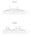
- FIGS. 1A-1Cshow views of an initial structure in an exemplary process flow for making an exemplary embodiment of the present device, in layout (e.g., top down) view ( FIG. 1A ) and cross-sectional views ( FIGS. 1B-1C ).
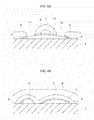
- FIGS. 2A-2Bshow cross-sectional views of an intermediate structure in the exemplary process flow.
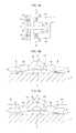
- FIGS. 3A-3Cshow views of a successive intermediate structure in the exemplary process flow for making an exemplary embodiment of the present device, in layout view ( FIG. 3A ) and cross-sectional views ( FIGS. 3B-3C ).
- FIGS. 4A-4Bshow cross-sectional views of a successive intermediate structure in the exemplary process flow.
- FIG. 5Ashows a top-down view of an exemplary embodiment of a nonvolatile memory device according to the present invention.
- FIGS. 5B-5Cshow cross-sectional views of an exemplary embodiment of a nonvolatile memory device according to the present invention along the A-A′ of FIG. 5A .
- FIGS. 6A-6Cshow cross-sectional views of successive intermediate structures in an exemplary alternative process flow for making a nonvolatile memory device according to the present invention.
- FIG. 7is a graph showing retention data for an exemplary EEPROM cell, in which the channel island/control gate layer was formed from a spin-coated silicon-containing ink.
- a nonvolatile memory cell according to the inventionmay be created using a printed TFT process flow with a single floating gate and one or two gate oxides. Two separate silicon islands may be used, one of which serves as a control gate and the other as source, drain and channel of the read transistor. The area ratio of the silicon islands to the floating gate (and to each other) may be chosen so as to achieve the desired capacitance coupling ratio(s).
- the devicemay be typically programmed using Fowler-Nordheim tunneling or hot injection of carriers across the tunnel gate oxide into the floating gate.
- a reference celle.g., an “unprogrammed” transistor, or one storing a “0” binary logic state
- a reference cellmay be programmed using the opposite bias from the programmed cell(s), leading to a greater delta V t between the programmed-unprogrammed cell pairs (e.g., the “0” and “1” binary logic states), enhancing the margin over which the cell is functional, thereby increasing retention time and/or allowing operation under less stringent (e.g., subthreshold swing) conditions. Charge is retained in the floating gate, resulting in a threshold voltage shift of the programmed transistor from a reference (unprogrammed) transistor.
- the transistoris read using a significantly lower voltage than that used during the programming operation, such that the charge on the floating gate is not substantially disturbed.
- a printed TFT logic processsuch as is described in any of U.S. Provisional Pat. Appl. No. 60/838,125, filed on Aug. 15, 2006, and/or U.S. patent application Ser. Nos. 11/084,448, 11/203,563, 11/452,108, 11/805,620, 11/818,078, 11/888,949 and 11/888,942, (filed on Mar. 18, 2005, Aug. 11, 2005, Jun. 12, 2006, May 23, 2007, Jun. 12, 2007, Aug. 3, 2007 and Aug. 3, 2007, respectively, the relevant portions of which are incorporated herein by reference) may be used, without extra processing steps, to manufacture the present nonvolatile memory transistors.
- the present memory cellmay be fabricated in part by printing a silicon ink to form the active transistor layer(s).
- sequential lateral laser solidification and/or crystallization of printed islands of siliconcan improve carrier mobility and gate oxide interface quality. This in turn significantly improves the TFT subthreshold slope (steeper turn on characteristics), which allows for a better separation between the zero and one states.
- Device feasibilityhas been demonstrated with excellent retention using a film made from a spun-on silicon ink and a printed/conventional TFT process flow (e.g., as described in one or more of the above-cited patent applications), with no extra processing steps required.
- the terms “coupled to,” “connected to,” and “in communication with”mean direct or indirect coupling, connection or communication, unless the context clearly indicates otherwise. These terms are generally used interchangeably herein, and wherever one such term is used, it also encompasses the other terms, unless the context clearly indicates otherwise.
- the term “deposit”(and grammatical variations thereof) is intended to encompass all forms of deposition, including blanket deposition, coating, and printing.
- the phrase “consisting essentially of”does not exclude intentionally added dopants, which may give the material to which the dopant is added (or the element or structure formed from such material) certain desired (and potentially quite different) physical and/or electrical properties.
- (poly)silanerefers to compounds or mixtures of compounds that consist essentially of (1) silicon and/or germanium and (2) hydrogen, and that predominantly contain species having at least 15 silicon and/or germanium atoms. Such species may contain one or more cyclic rings.
- the (poly)silanehas a formula Si x H y , where x is from 3 to about 200, and y is from x to (2x+2), where x may be derived from an average number molecular weight of the silane.
- (cyclo)silanerefers to compounds or mixtures of compounds that consist essentially of (1) silicon and/or germanium and (2) hydrogen, and that may contain one or more cyclic rings and less than 15 silicon and/or germanium atoms.
- hetero(cyclo)silanerefers to compounds or mixtures of compounds that consist essentially of (1) silicon and/or germanium, (2) hydrogen, and (3) dopant atoms such as B, P, As or Sb that may be substituted by a conventional hydrocarbon, silane or germane substituent and that may contain one or more cyclic rings.
- “Liquid-phase”generally describes one or more materials that, alone or in combination, are in the liquid phase at an ambient temperature (e.g., from about 15° C.
- a “major surface” of a structure or featureis a surface defined at least in part by the largest axis of the structure or feature (e.g., if the structure is round and has a radius greater than its thickness, the radial surface[s] is/are the major surface of the structure; however, where the structure is square, rectangular or oval, the major surface of the structure is typically a surface defined by the two largest axes, generally the length and width).
- the inventionis particularly applicable to printed silicon, metal silicide or refractory metal structures in an “all-printed” process flow.
- Polysilicon, metal silicidese.g. Ni-, Pt-, Pd, Co-, Ti, W, Mo-silicides and others
- refractory metalssuch as Pd, W or Mo, etc.
- the “all-printed” aspectalso allows the use of printed (e.g., inkjetted) doped dielectrics as dopant sources in a self-aligned flow.
- FIGS. 1A-5Bshow an exemplary process flow for making printed non-volatile memory (e.g., an “all-printed” EEPROM transistor).
- FIGS. 1A-1Cshow a substrate 1 (not shown in FIG. 1A ) with a control gate 2 and transistor island 3 thereon.
- FIG. 1Bis a cross-sectional view of the structure of FIG. 1A along axis A-A′
- FIG. 1Cis a cross-sectional view of the structure of FIG. 1A along axis B-B′.
- Substrate 1generally comprises a conventional mechanical support structure, which may be electrically inert or active, and which may further include one or more advantageous and/or desired electrical and/or optical properties.
- Suitable electrically inert or inactive substratesmay comprise a plate, disc, and/or sheet of a glass, ceramic, dielectric and/or plastic.
- suitable electrically conductive substratesmay comprise a wafer, disc, sheet and/or foil of a semiconductor (e.g., silicon) and/or a metal.
- the substratecomprises a metal sheet and/or foil
- the devicemay further comprise an inductor and/or capacitor
- the methodmay further comprise forming an inductor and/or capacitor from the metal substrate.
- any such electrically conductive substrateshould have an insulator layer between it and any electrically active layer or structure thereover, except in a location where electrical contact is to be made from the structures and/or devices on the insulator to a structure formed in the metal substrate (e.g., one or more metal pads of an interposer, an inductor and/or capacitor; see, e.g., U.S. patent application Ser. Nos. 10/885,283, 11/104,375 and 11/243,460, respectively filed on Jul. 6, 2004, Apr. 11, 2005, and Oct. 3, 2005, the relevant portions of which are incorporated herein by reference).
- a structure formed in the metal substratee.g., one or more metal pads of an interposer, an inductor and/or capacitor; see, e.g., U.S. patent application Ser. Nos. 10/885,283, 11/104,375 and 11/243,460, respectively filed on Jul. 6, 2004, Apr. 11, 2005, and Oct. 3, 2005, the relevant portions of which are incorporated here
- the substrate 1comprises a member selected from the group consisting of a silicon wafer, a glass plate, a ceramic plate or disc, a plastic sheet or disc, metal foil, a metal sheet or disc, and laminated or layered combinations thereof.
- plastic substratesmay further contain a planarization layer thereon to reduce the surface roughness of the substrate
- glass, steel and plastic substratesmay further contain a surface energy modifying layer of material thereon to improve the adhesion and/or control the spreading of a material (e.g., an ink) printed or otherwise deposited thereon (see U.S. Provisional Application No. 60/919,290, filed on Mar. 20, 2007).
- the electrically conductive substrates(e.g., comprising or consisting essentially of a metal) generally have an insulator layer (e.g., a layer of the corresponding metal oxide) and/or a substantially amorphous conductive layer (e.g., a transition metal nitride, such as titanium nitride, tantalum nitride, or tungsten nitride) thereon.
- an insulator layere.g., a layer of the corresponding metal oxide
- a substantially amorphous conductive layere.g., a transition metal nitride, such as titanium nitride, tantalum nitride, or tungsten nitride
- semiconductor islands 2 and 3are formed by printing or coating molecular and/or nanoparticle-based semiconductor inks, which in the case of printing can use the same or different inks, then converting them to thin films (e.g., by heating and/or curing).
- the molecular-based semiconductor inkcomprises a (poly)silane and/or (cyclo)silane
- the nanoparticle-based semiconductor inkcomprises silicon nanoparticles
- the semiconductor thin filmcomprises a (poly)silicon film.
- inkscomprising both (i) a (poly)silane and/or (cyclo)silane, and (ii) silicon nanoparticles are perfectly suitable.
- printingmay comprise inkjet printing (“inkjetting”), screen printing, gravure printing, offset printing, flexography (flexographic printing), spray-coating, slit coating, extrusion coating, meniscus coating, microspotting, pen-coating, stenciling, stamping, syringe dispensing and/or pump dispensing the semiconductor ink in a predefined pattern onto substrate 1 .
- inkjettinginkjet printing
- screen printinggravure printing
- offset printingoffset printing
- flexographyflexographic printing
- spray-coatingslit coating, extrusion coating, meniscus coating, microspotting
- pen-coatingstenciling
- stampingstamping
- syringe dispensingand/or pump dispensing the semiconductor ink ink in a predefined pattern onto substrate 1 .
- printingcomprises inkjetting, gravure printing, offset printing, or flexography.
- Forming the semiconductor thin film layers 2 and 3may thus include printing a semiconductor precursor ink onto substrate 1 (generally having a dielectric material on the deposition surface) to form a pattern, drying the ink, curing the ink (generally by heating and/or annealing the dried ink for a length of time sufficient to cross-link, oligomerize and/or polymerize the silane, and/or increase an average molecular weight, increase a viscosity and/or reduce a volatility of the composition), then partially or substantially completely crystallizing the semiconductor film pattern to form a polycrystalline (e.g., polysilicon) film.
- a semiconductor precursor ink onto substrate 1generally having a dielectric material on the deposition surface
- curing the inkgenerally by heating and/or annealing the dried ink for a length of time sufficient to cross-link, oligomerize and/or polymerize the silane, and/or increase an average molecular weight, increase a viscosity and/or reduce a volatility of the
- printing (or otherwise depositing) the semiconductor inkmay be accompanied by substantially simultaneous or immediately subsequent irradiation with light (in one embodiment, UV light), generally at a wavelength and/or in a dose sufficient to cross-link the silicon-containing components of the ink, improve adhesion of the film to the substrate, and/or improve the film morphology (e.g., provide a desired cross-sectional shape).
- lightin one embodiment, UV light
- a substantial advantage of the present processis that the printed semiconductor island may have a tapered, dome-like cross-sectional shape, allowing for conformal formation of gate dielectric through deposition or thermal oxidation.
- Forming a plurality of semiconductor islandsmay be done by printing a liquid-phase semiconductor ink, preferably an ink that comprises a liquid-phase (poly)- and/or (cyclo)silane in an amount of from 1 to 50 wt. % of the ink, and a solvent in which the silane is soluble, optionally in the presence of or onto a crystallization promoter such as Au, Ni, Al, etc.
- liquid-phase semiconductor inkstypically, although not necessarily always, liquid-phase semiconductor inks further comprise a solvent, preferably a cycloalkane.
- forming the semiconductor layermay further comprise drying the liquid-phase precursor ink after deposition.
- a Group IVA element sourcesuch as a silane-based precursor to Si or doped Si
- the silanehas the formula Si x H y , where x is from 3 to 1000, and y is from x to (2x+2), where x may be derived from an average number molecular weight of the silane.
- the semiconductor inkmay further comprise silicon nanocrystals, which may be passivated with one or more ligands selected from the group consisting of alkyl groups, aralkyl groups, alcohols, alcoholates, thiols, thiolates, hydrogen and/or carboxylates (see, e.g., U.S. patent application Ser. No. 10/616,147, filed on Jul. 8, 2003, the relevant portions of which are incorporated herein by reference).
- Representative cyclosilane compounds of the formula (AH z ) k wherein A is Si, z is 1 or 2 (preferably 2) and k is from 3 to 12 (preferably 4 to 8) and an exemplary method for their preparationare described in greater detail in copending application Ser. No. 10/789,317, filed Feb. 27, 2004, the relevant portions of which are incorporated herein by reference.
- one or more of the A atomsmay be Ge.
- Representative hetero(cyclo)silane compounds, doped silane intermediates, doped silane compositions, exemplary methods for their preparation, and techniques for determining and/or controlling the dopant levels in the precursor inks and active filmsare described in greater detail in copending U.S. patent application Ser. Nos.
- a semiconductor layeris generally cured by heating, as described above in copending U.S. patent application Ser. No. 10/789,274 and 10/949,013,(filed on Feb. 27, 2004 and Sep. 24, 2004, the relevant portions of which are incorporated herein by reference) to form an amorphous, hydrogenated (doped) semiconductor (e.g., a-Si:H) layer.
- amorphous, hydrogenated (doped) semiconductore.g., a-Si:H
- the curing/heating stepmay remove unwanted precursor/ink components or byproducts such as volatile carbon-containing species, or reduce the hydrogen content of the amorphous, hydrogenated semiconductor (e.g., a-Si:H) layer (which is particularly advantageous if laser crystallization is to be used after semiconductor film formation).
- amorphous, hydrogenated semiconductore.g., a-Si:H
- the curing/heating stepmay also activate part of the dopant in the hetero(cyclo)silane, but in many embodiments, dopant activation may be more likely to occur during a subsequent laser crystallization step.
- a semiconductor filme.g., by evaporation, physical vapor deposition, sputtering of an elemental target, or chemical vapor deposition [e.g., PECVD, LPCVD, etc.]
- a crystallization promotersuch as Au, Ni, Al, etc.
- “low-resolution photolithography”refers to photolithography having a minimum line width on the order of microns (e.g., 1 ⁇ m, 2 ⁇ m, 5 ⁇ m or more), as opposed to submicron photolithography.
- the semiconductor filmis crystallized by laser annealing, one may simply remove the non-irradiated, amorphous portions of the deposited film by selective etching in accordance with known techniques.
- semiconductor layers 2 and 3comprise or consist essentially of a lightly doped inorganic semiconductor material, such as one or more Group IVA elements (e.g., silicon and/or germanium), a so-called “III-V” material (e.g., GaAs), a II-VI (or chalcogenide) semiconductor, etc., which may further contain a dopant (such as B, P, As or Sb) in a concentration of from ⁇ 10 16 to ⁇ 5 ⁇ 10 18 atoms/cm 3 .
- the semiconductor thin film layers 2 and 3generally comprise or consist essentially of one or more Group IVA elements, preferably silicon or silicon-germanium.
- the semiconductor channel island 3may be lightly doped (e.g., having a dopant concentration of from about 10 16 to about 10 18 atoms/cm 3 ).
- lightly doped semiconductor films and methods of forming the sameare disclosed in copending U.S. application Ser. Nos. 10/950,373, 10/949,013 and 10/956,714, respectively filed on Sep. 24, 2004, Sep. 24, 2004 and Oct. 1, 2004, the relevant portions of which are incorporated herein by reference.
- the lightly doped semiconductor filmWhen formed from a silane-based ink, the lightly doped semiconductor film may have a concentration profile (e.g., dopant concentration as a function of semiconductor layer thickness) in an amorphous state that is substantially uniform throughout substantially the entire thickness of the semiconductor layer.
- Typical thicknesses for semiconductor layers 2 and 3may be from about 10, 25, 50, or 100 nm to about 200, 500 or 1000 nm, or any range of values therein.
- the film thicknessmay be chosen to optimize the electrical properties of the non-volatile memory transistor.
- semiconductor layers 2 and 3may have a width (e.g., the longest dimension shown in the cross-section A-A′ of FIGS. 1A-1B ) of at least 5, 8 or 10 ⁇ m, up to 50, 100, or 200 ⁇ m or more, or any range of values therein.
- the channel island 3may have a length (e.g., the horizontal dimension shown in FIG. 1C ) of at least 1, 2, 5, 10 or 20 ⁇ m, up to 20, 50 or 100 ⁇ m or more, or any range of values therein.
- Each of the first and second semiconductor islands 2 and 3has an area defined by a width and a length.
- the width and/or length of the first semiconductor islande.g., control gate 2
- the width and/or length of the second semiconductor islande.g., channel island 3
- the predetermined distance between the islandsis from 1 to 50 ⁇ m, preferably from 2 or 5 ⁇ m to 20 or 25 ⁇ m (or any range of values therein).
- the printed (or deposited) and cured semiconductor islands 2 and 3may be further (re)crystallized by sequential lateral solidification (SLS) and/or laser crystallization to improve carrier mobility and gate oxide interface quality.
- SLSsequential lateral solidification
- Such (re)crystallizationmay significantly improve the TFT subthreshold slope (e.g., provide steeper turn on characteristics), which allows for a better separation between the zero and one states stored in the memory cell.
- FIGS. 2A-2Bshow the formation of dielectric layers 4 and 5 on the control gate 2 and transistor island 3 .
- FIG. 2Ais a cross-sectional view along axis A-A′ of a structure as shown in FIG. 1A (see, e.g., FIG. 1B ), and
- FIG. 2Bis a cross-sectional view along axis B-B′ of a structure as shown in FIG. 1A (see, e.g., FIG. 1C ).
- dielectric layers 4 and 5may be the same or different.
- different (doped) oxides and/or different oxide thicknessescan be grown thereon, as is known in the art.
- Dielectric layers 4 and 5can be formed by plasma-enhanced chemical vapor deposition (PE-CVD), low pressure, atmospheric pressure or high pressure chemical vapor deposition (LPCVD, APCVD, and HPCVD, respectively), thermal oxidation in an atmosphere containing an oxidizing and/or nitriding agent (e.g., dioxygen, ozone, water vapor, dinitrogen, nitrous oxide, nitric oxide, NO, ammonia, a combination thereof, etc.), chemical (bath) deposition of a metal oxide (e.g., SiO 2 from aqueous hydrosilicic acid, H 2 SiF 6 ), liquid phase deposition of a dielectric film precursor and subsequent conversion to a dielectric film, atomic layer deposition, or a combination thereof.
- PE-CVDplasma-enhanced chemical vapor deposition
- LPCVDlow pressure, atmospheric pressure or high pressure chemical vapor deposition
- HPCVDhigh pressure chemical vapor deposition
- forming the gate dielectric layer 4 and the tunnel dielectric layer 5may comprise plasma or low-pressure chemical vapor deposition of the dielectric layer, thermal oxidation of a surface of the control gate 2 and semiconductor island 3 , or liquid phase or chemical bath deposition of gate and tunnel dielectric precursors onto the control gate 2 and transistor island 3 .
- the gate dielectric layers 4 and 5may comprise a plurality of layers and/or be formed on all of the plurality of semiconductor islands 2 and 3 .
- a preferred embodiment of the present inventioncomprises forming a gate dielectric layer (e.g., 4 and/or 5 ) on or over at least a subset of a plurality of semiconductor islands 2 or 3 .
- Semiconductor islands not having a dielectric layer formed thereonmay be used for devices such as diodes (e.g., Schottky diodes), resistors, etc.
- oxidation of the silicon-containing filmcan be accomplished by heating the film in a suitable atmosphere (air, O 2 , ozone, N 2 O or steam, or combinations thereof) to a temperature higher than about 600° C., preferably at least about 800° C., more preferably at least about 850° C.
- the maximum temperaturemay be about 1000-1100° C., more preferably about 900° C., to reduce, inhibit or prevent thermal damage (if any) to the substrate and/or films or structures thereon.
- a stainless steel film, sheet or foilmay be a particularly advantageous choice for the substrate 1 .
- the gate dielectric film 4 or 5may have a thickness of from 20 ⁇ to 400 ⁇ or any range of values therein (e.g., from 30 to 300 ⁇ , or from 50 to 200 ⁇ , etc.).
- the higher temperature processes enabled by a stainless steel foiltypically enable substantially enhanced gate dielectric properties, including lower defect rates, a lower number/concentration of interface states and lower leakage, which translates to superior subthreshold swing, carrier mobility and data retention.
- the present methodmay further comprise forming a floating gate 7 on the gate dielectric layers 4 and 5 and on or over some or all of the plurality of semiconductor islands 2 and 3 .
- FIG. 3Ashows a top-down (layout) view of control gate 2 and transistor island 3 , with floating gate 7 thereon.
- FIG. 3Bis a cross-sectional view of the structure of FIG. 1A along axis A-A′
- FIG. 3Cis a cross-sectional view of the structure of FIG. 3A along axis B-B′.
- the floating gate 7may be formed by printing a suitable precursor (e.g. metal nanoparticles or organometallic compound(s), doped molecular and/or nanoparticle-based silicon ink(s), silicide precursor ink(s), etc.), then converting it to a floating gate conductor, suitable for storing electrical charge.
- a suitable precursore.g. metal nanoparticles or organometallic compound(s), doped molecular and/or nanoparticle-based silicon ink(s), silicide precursor ink(s), etc.
- a suitable precursore.g. metal nanoparticles or organometallic compound(s), doped molecular and/or nanoparticle-based silicon ink(s), silicide precursor ink(s), etc.
- a suitable precursore.g. metal nanoparticles or organometallic compound(s), doped molecular and/or nanoparticle-based silicon ink(s), silicide precursor ink(s), etc.
- forming the floating gate 7may comprise printing a seed layer on the gate dielectric layers 4 and 5 , then electro- or electrolessly plating a floating gate material on the seed layer.
- the floating gate 7may comprise a printed material, generally made of doped polysilicon, a metal silicide or a refractory metal.
- the floating gate 7comprises a doped Group IVA element.
- the doped Group IVA elementcomprises polysilicon containing an N-type dopant.
- the N-type dopantcomprises phosphorous.
- the floating gate 7comprises a metal silicide selected from the group consisting of nickel silicide, cobalt silicide, palladium silicide, platinum silicide, titanium silicide, tungsten silicide, and molybdenum silicide.
- the floating gate 7comprises a refractory metal selected from the group consisting of palladium, tungsten, and molybdenum.
- the floating gate 7comprises aluminum.
- Printing the floating gate precursor 7 and/or seed layermay include any of the printing techniques described above for forming the semiconductor islands 2 and 3 (e.g., ink-jetting, gravure printing, offset lithography, etc.).
- patterning the floating gate 7may include coating or printing the floating gate precursor and locally exposing it to laser radiation such that the radiated portion changes its solubility characteristics in the exposed areas. Upon washing away the exposed or unexposed area (depending on whether the precursor is a positive or negative patternable material), the floating gate material (or its precursor) stays behind to form the floating gate 7 , optionally after an additional curing or annealing step.
- This embodimentmay provide advantages for the patterning of high-resolution metal gates which may not directly be achievable with direct printing methods (see, e.g., copending U.S. patent application Ser. No. 11/203,563, filed on Aug. 11, 2005, the relevant portions of which are incorporated herein by reference).
- the silicon precursor inkmay comprise a (poly)silane, (cyclo)silane and/or silicon nanocrystals (each of which may be present in an amount of, e.g., from 1 to 50 wt. % of the ink, or any range of values therein, such as 5 to 20 wt. %) and a solvent in which the silane and/or silicon nanocrystals are soluble.
- the silicon nanocrystalsmay be passivated and/or functionalized to enable light-based processing (e.g., laser writing; see, e.g., U.S. patent application Ser. Nos.
- the silane ink compoundsmay optionally be doped as disclosed in U.S. patent application Ser. Nos. 10/949,013, 10/950,373, and 10/956,714, filed on Sep. 24, 2004, Sep. 24, 2004, and Oct. 1, 2004, the relevant portions of each of which is incorporated herein by reference).
- the printed silane inkis cured to form (optionally doped) amorphous silicon films.
- Such filmscan be further crystallized using conventional methods (e.g., laser, furnace or metal-induced crystallization) to form (optionally doped) polycrystalline silicon.
- dopingmay be accomplished by implantation, or more preferably, by doping from a printed doped oxide (see the description herein) to form the printed floating gate 7 .
- Such silane inks and processes of making and using the samecan also be used to form the semiconductor islands 2 and 3 , as may the sequential lateral solidification (SLS) and/or laser crystallization techniques for (re)crystallizing the printed floating gate 7 , but the effect on carrier mobility, oxide interface quality, and subthreshold slope may be less significant than for the semiconductor islands 2 and 3 .
- SLSsequential lateral solidification
- laser crystallization techniquesfor (re)crystallizing the printed floating gate 7 , but the effect on carrier mobility, oxide interface quality, and subthreshold slope may be less significant than for the semiconductor islands 2 and 3 .
- the precursor inkmay comprise nanoparticles and/or molecular, oligomeric and/or polymeric compounds of silicon and silicide forming metals (e.g. Ni, Co, Pd, Pt, Ti, W, Mo etc.), in the same loading (e.g., weight %) as the silane/silicon ink above.
- the metal atom/Si atom ratio in the silicide precursor inkmay range from 10/1 to 1/10.
- the inkcomprises (poly)- and/or (cyclo)silane compounds as mentioned above and nanoparticles (see the next paragraph) and/or organometallic compounds of silicide forming metals (e.g., Ni(PPH 3 ) 4 , Ni(COD) 2 , Ni(PF 3 ) 4 , etc., for example to facilitate formation of low resistance contacts).
- the floating gate precursor inkmay comprise (i) a (poly)silane, (ii) metal nanoparticles and/or an organometallic compound, and (iii) a solvent in which the (poly)silane and the metal nanoparticles and/or the organometallic compound are soluble.
- a metal-containing inkmay comprise or consist essentially of a metal precursor material and a solvent in which the metal precursor material is soluble.
- Metal precursors that are generally compatible with printing or (selective) platingmay comprise compounds or nanoparticles (e.g., nanocrystals) of a metal such as titanium, copper, silver, chromium, molybdenum, tungsten, cobalt, nickel, gold, palladium, platinum, zinc, iron, etc., or metal alloys thereof.
- the metal precursor inkmay comprise nanoparticles and/or molecular or oligomeric compounds of refractory metals (e.g., Pd, Mo, W, etc.), in the same loading (e.g., weight %) as the silane/silicon ink above.
- refractory metalse.g., Pd, Mo, W, etc.
- molecular or oligomeric metal compoundsinclude carboxylate, acetylacetonate, allyl, phosphine, carbonyl, and/or other ligand complexes of such metals.
- Pdinks including solubilized palladium halides (PdCl 2 in aqueous HCl and a polar or water-soluble organic solvent, which may be dried to remove some or all of the water) can be used.
- Metal nanoparticles or nanocrystalsmay be conventionally passivated (e.g., with one or more surfactants, ligands or substituent groups as described herein) or unpassivated.
- the metal floating gate 7may be formed as a mixture of two or more metals, or as laminated layers (as may the semiconductor and metal silicide floating gates), and may be further heated or otherwise thermally processed during or after formation of successive layers. After printing the refractory metal precursor ink, the printed film is cured and annealed under conditions (e.g., atmosphere, temperature and time) which facilitate the formation of the intended refractory metal (and/or phase thereof).
- the metal- and/or silicon-containing inkmay be dried by conventional and/or otherwise known processes.
- precursor inksmay be dried by heating the substrate containing the printed precursor ink thereon at a temperature and for a length of time effective to remove the solvent and/or binder.
- Suitable temperatures for removing solvents from a printed inkmay range from about 80° C. to about 150° C., or any range of temperatures therein (e.g., from about 100° C. to about 120° C.).
- Suitable lengths of time for removing solvents from a printed ink at such temperaturesmay ranges from about 10 seconds to about 10 minutes, or any range of times therein (e.g., from about 30 seconds to about 5 minutes, or about 1 minute to 3 minutes, etc.).
- Such heatingmay take place on a conventional hotplate or in a conventional furnace or oven, optionally in an inert atmosphere (as described above).
- the dried precursor material from the inkmay be further annealed at a temperature and for a length of time sufficient to improve its electrical and/or physical properties (e.g., conductivity, morphology, electromigration and/or etch resistance, stress and/or surface strain, etc.) and/or its adhesion to the underlying gate oxide 4 and/or tunnel oxide 5 .
- electrical and/or physical propertiese.g., conductivity, morphology, electromigration and/or etch resistance, stress and/or surface strain, etc.
- adhesion to the underlying gate oxide 4 and/or tunnel oxide 5e.g., annealing is generally conducted to form a metal film on which a resist is deposited for subsequent (laser) patterning.
- annealingis generally performed to form a metal layer with improved properties (e.g., conductivity, adhesion, etc.).
- annealingmay comprise either annealing of already-fused metal nanoparticles, or converting a patterned metal precursor layer into a patterned metal.
- Suitable temperaturesgenerally range from about 100° C. to about 300° C., or any range of temperatures therein (e.g., from about 150° C. to about 250° C.).
- Suitable lengths of time for annealingmay range from about 1 minute to about 2 hours, preferably from about 10 minutes to about 1 hour, or any range of times therein (e.g., from about 10 to about 30 minutes).
- Annealingmay be conducted in a conventional furnace or oven, optionally in an inert or reducing atmosphere (as described above).
- the present methodmay further comprise the step of annealing the laser patterned metal gate sufficiently to improve its electrical, physical and/or adhesive properties.
- Metal inks that may be deposited by spin-coating or printinginclude precursors of elemental metals, such as aluminum, titanium, vanadium, chromium, molybdenum, tungsten, iron, nickel, palladium, platinum, copper, zinc, silver, gold, etc.; conventional alloys of such elements, such as aluminum-copper alloys, aluminum-silicon alloys, aluminum-copper-silicon alloys, titanium-tungsten alloys, Mo—W alloys, aluminum-titanium alloys, etc.; and electrically conductive metal compounds, such as the nitrides and silicides of elemental metals (e.g., titanium nitride, titanium silicide, tantalum nitride, cobalt silicide, molybdenum silicide, tungsten silicide, platinum silicide, etc.).
- elemental metalssuch as aluminum, titanium, vanadium, chromium, molybdenum, tungsten, iron, nickel, palladium, platinum,
- suitable precursors of elemental aluminuminclude aluminum nanoparticles and aluminum hydrides.
- the metalmay by blanket deposited by spin-coating an ink containing the metal-containing material and curing or annealing the metal, organometallic precursor(s) and/or metal nanoparticles (optionally before a laser patterning step).
- Platingmay comprise, in one example, printing or laser writing a seed layer of metal (e.g., Pd) using nanoparticle- and/or compound-based metal ink (e.g., the PdCl 2 -containing ink described above), then selectively depositing (e.g., by electroless or electroplating) a bulk conductor (e.g., Co, Ni, Cu, Pd, etc.) onto the metal seed layer.
- a seed layer of metale.g., Pd
- nanoparticle- and/or compound-based metal inke.g., the PdCl 2 -containing ink described above
- a bulk conductore.g., Co, Ni, Cu, Pd, etc.
- metal nanoparticlescomprising cobalt, nickel, platinum, palladium, titanium, tungsten or molybdenum (particularly palladium) are preferred for the seed layer.
- laser writing or laser patterningmay comprise the substeps of depositing a resist material on the blanket deposited metal-containing layer, selectively irradiating portions of the resist material with a beam of light from a laser having (i) a predetermined width and/or (ii) a predetermined wavelength or wavelength band absorbed by the resist (or by an absorptive dye in the resist), developing the selectively irradiated resist with a developer to leave a pattern corresponding to the structure being formed (in this case, gate metal 20 ; note that these steps apply to both positive and negative resists), removing those portions of the blanket deposited material not corresponding to the desired or predetermined pattern (typically by dry or wet etching), and removing the remaining resist material.
- the lighthas a wavelength in the infrared (IR) band (although it could also comprise a wavelength or wavelength band in the ultraviolet (UV) and/or visible band of the spectrum), the resist (or dye) absorbs and/or is sensitive to that wavelength or band of light, and the light beam is focused on or directed at the desired or predetermined portions of the resist.
- IRinfrared
- UVultraviolet
- UVultraviolet
- a thermal resistmay be advantageously used to mask the floating gate metal. Irradiation of the thermal resist with a relatively narrow laser beam (e.g., 2-5 ⁇ m wide, or by passing more diffuse light through a mask configured to define structures of such width) from a laser heats the resist and changes its solubility characteristics in a conventional developer that is used to remove the irradiated (written) or non-irradiated (unwritten) portions of the resist, depending on whether the resist is positive- or negative-acting, respectively.
- Such resistsare generally available commercially from Creo Inc., Burnaby, British Columbia, Canada.
- Preferred thermal resistsinclude Graviti Thermal Resist (Creo) and the American Dye Sources Thermolak series.
- the resistmay also comprise a conventional (photo)resist material having an infrared (IR) light-absorbing dye therein.
- Preferred (photo)resistsinclude AZ1518 (AZ Electronic Materials) and SPR220 (Shipley), and preferred infrared (IR) light-absorbing dyes include American Dye Source 815I, 830AT, 830WS and 832WS, Avecia Projet 830NP and 830 LDI, Epolin Epolight 4148, 2184, 4121, 4113, 3063 and 4149, HW Sands SDA5303 and SDA4554.
- metal (or metal precursor) material outside of the (predetermined) gate patternmay be removed by wet or dry etching. Wet etching may also advantageously undercut the resist to provide an even narrower gate and/or transistor channel width than would be possible using dry etching.
- the floating gate 7has a width of at least 0.1 microns, 0.5 microns, 1 micron, or 2 microns. In one implementation, the minimum gate width is about 5 microns.
- the floating gate 7may have a length of from about 1 ⁇ m to about 1000 ⁇ m or any range of values therein (e.g., from about 2 ⁇ m to about 200 ⁇ m, or from about 5 ⁇ m to about 100 ⁇ m, etc.), and a thickness of from about 50 nm to about 10,000 nm or any range of values therein (e.g., from about 100 to about 5000 nm, or from about 200 to about 2000 nm, etc.).
- the floating gate 7may also have a thickness of from 10 to 1000 nm or any range of values therein (e.g., from 100, 200, or 250 ⁇ to 10,000, 1000, or 500 ⁇ ).
- exposed portions of the gate dielectric layer 4 and the tunnel dielectric layer 5may be conventionally removed (e.g., by wet or dry etching; see, e.g., FIG. 6A , discussed below).
- a first doped dielectric layer (ILD) 8may be printed or deposited on the floating gate 7 , exposed portions of the gate dielectric 4 and tunnel dielectric 5 over semiconductor islands 2 and 3 , and the surface of substrate 1 .
- FIG. 4Ais a cross-sectional view along axis A-A′ of a structure as shown in FIG. 3A
- FIG. 4Bis a cross-sectional view along axis B-B′ of a structure as shown in FIG. 3A , with doped dielectric layer 8 printed or deposited thereon.
- the dielectric film 8contains a diffusible dopant.
- the dopantis an N-type dopant, preferably comprising phosphorous.
- the diffusible dopantmay comprise a P-type dopant, preferably comprising boron.
- the control gate 2 , the transistor island 3 (including source and drain terminals therein), and (optionally) the floating gate 7may comprise (i) a Group IVA element, a III-V compound semiconductor such as GaAs, or a II-VI (or chalcogenide compound) semiconductor such as ZnO or ZnS, and (ii) a dopant element.
- the semiconductorcomprises a Group IV element (e.g., Si and/or Ge) and a dopant selected from the group consisting of B, P, As and Sb.
- the doped dielectric film 8may be printed such that contact holes 11 and 12 are formed in the dielectric film 8 , to expose an upper surface of the gate dielectric 4 over the control gate 2 on opposed sides of the floating gate 7 .
- similar contact holesare formed in the dielectric film 8 to expose an upper surface of the tunnel dielectric 5 over the semiconductor island 3 on opposed sides of the floating gate 7 (see, e.g., FIG. 5A ).
- the pattern in which the doped dielectric layer 8 is printedincludes a contact hole in such locations.
- the doped dielectric film 8is generally printed onto the entire surface of the floating gate 7 .
- the exposed gate dielectric 4 and tunnel dielectric 5may then be etched (by either conventional wet or dry etching, as discussed below, and either before or after annealing to diffuse the dopant) to form structures 4 ′ and 10 in FIG. 4A and expose a surface of control gate 2 .
- the doped dielectric layer 8may also be etched sufficiently to widen the contact holes 11 and 12 , preferably such that a dielectrically effective thickness of the doped dielectric layer 8 remains after etching.
- the doped dielectric 8may be printed in a pattern covering the entirety of the control gate 2 , the transistor island 3 , and the floating gate 7 .
- the doped dielectric layer 8may be printed over an even larger area, comprising an entire memory cell (e.g., at least the layout of FIG. 5A ) or a plurality of adjacent memory cells.
- the contact holese.g., 11 and 12 in FIG. 4A
- the doped dielectric layer 8are formed in the doped dielectric layer 8 to expose upper surface areas of the control gate 2 and source/drain terminals in the semiconductor island 3 (e.g., under and in electrical contact with metal interconnects/contacts 14 and 15 in FIG. 5A ).
- the contact holesare formed by photolithography and etching (see, e.g., the description in the following paragraph).
- forming contact holes 11 and 12may comprise removing portions of a first and second type of dielectric layer 8 , particularly when the printed pattern for doped dielectric 8 does not include any contact holes.
- Etching of the doped glass pattern and gate dielectricis accomplished by exposure to one or more suitable etchants including, but not limited to, HF-based wet etchants (e.g., buffered oxide etch [BOE], native oxide etch [NOE], aq. pyridine:HF, etc.), HF-based or HF-producing vapors or gases, plasma etching, etc.
- suitable etchantsincluding, but not limited to, HF-based wet etchants (e.g., buffered oxide etch [BOE], native oxide etch [NOE], aq. pyridine:HF, etc.), HF-based or HF-producing vapors or gases, plasma etching, etc.
- suitable etchantsincluding, but not limited to, HF-based wet etchants (e.g., buffered oxide etch [BOE], native oxide etch [NOE], aq. pyridine:HF, etc.), HF-based or HF-producing vapors or gases,
- the etchantis chosen such that the etch rate of the doped dielectric layer 8 , the gate dielectric 4 , and the tunnel dielectric 5 is sufficiently larger than the etch rate of the transistor island 3 (e.g., silicon) and control gate 2 to enable substantially complete removal of a desired and/or predetermined amount of the doped dielectric layer 8 , the gate dielectric 4 , and the tunnel dielectric 5 without substantial or significant removal of the transistor island 3 and control gate 2 .
- Suitable inks for printing the doped dielectric layer 8include compounds and/or polymers containing dopant and/or dielectric precursor atoms such as phosphorous and oxygen (which may further include silicon, carbon, hydrogen and/or nitrogen), boron (which may further include silicon, carbon, hydrogen, oxygen and/or nitrogen), arsenic and/or antimony (either of which may further include silicon, carbon, hydrogen and/or oxygen), etc., optionally in a suitable solvent (see, e.g., U.S. Provisional Pat. Appl. No. 60/838,125, and U.S. patent application Ser. Nos. 11/818,078, 11/888,949 and 11/888,942, filed on Jun. 12, 2007, Aug. 3, 2007 and Aug. 3, 2007, respectively, the relevant portions of which are incorporated herein by reference).
- Exemplary phosphorous-containing dielectricsinclude:
- Exemplary boron-containing dielectricsinclude:
- Exemplary arsenic and/or antimony-containing dielectricsinclude:
- precursors for the doped glassinclude conventional spin-on-dopant (SOD) formulations and versions thereof with increased viscosity (e.g., by replacing or diluting the solvent in the conventional formulation with a similar or compatible solvent of higher viscosity), doped molecular silicon ink formulations which can be oxidized at low temperatures (e.g. ⁇ 400° C.) after deposition (e.g.
- SODspin-on-dopant
- cyclic, linear or branched silane oligomers or polymerswhich may include one or more dopant substituents, such as cyclo-Si 5 H 9 PR 2 , wherein R is lower [C 1 -C 4 ] alkyl, phenyl or C 1 -C 4 -alkyl substituted phenyl, or a dopant precursor in the formulation [e.g. tert-butyl phosphine]; see U.S. patent application Ser. No. 10/949,013, filed on Sep. 24, 2004, the relevant portions of which are incorporated herein by reference), oxidized doped molecular silicon ink formulations (e.g.
- oxidized versions of cyclic, linear or branched silane oligomers or polymerse.g., cyclo-Si 5 O 5 H 10
- dopant precursors in the formulatione.g., mono-, di- or tri-tert-butylphosphine or oxidized analogs thereof
- glass forming formulationse.g., so-called sol-gel formulations
- phosphorous or boron compoundse.g., organophosphates such as di-n-butylphosphate, or organoborates such as tri-t-butylborate, etc.
- the doped dielectric 8can be blanket deposited over substantially the entire substrate (e.g., by coating or other blanket deposition techniques, such as conventional spin-coating, blade coating, dip coating, meniscus coating, slot coating, or spray coating a spin-on glass [SOG] ink composition comprising one or more conventional SOG components, one or more conventional solvents therefor, and optionally one or more conventional surfactants, tension reducing agents, binders and/or thickening agents), liquid phase deposition of a doped SiO 2 precursor (such as a tetraalkylsiloxane or tetraalkoxysilane containing one or more of dopant/dielectric sources listed above), chemical vapor deposition (CVD, PECVD, LPCVD, etc.) or sputter deposition of another metal oxide(s) (e.
- CVDchemical vapor deposition
- PECVDPECVD, LPCVD, etc.
- sputter deposition of another metal oxide(s)e.
- the doped dielectriccan be formed from a doped silane ink (as disclosed in the above-cited U.S. Patent Applications), which may be cured after printing in an oxidizing atmosphere.
- a doped silane inkcan be directly inkjetted onto the substrate, islands and floating gate, as disclosed in U.S. Provisional Appl. No. 60/926,125, filed Apr. 24, 2007, the relevant portions of which are incorporated by reference).
- the structureis annealed sufficiently to diffuse (“drive in”) the dopant from doped dielectric film 8 into the floating gate 7 (when the floating gate 7 includes or consists essentially of polysilicon) and the semiconductor islands 2 and 3 (although the dopant may not diffuse completely in the regions of semiconductor islands 2 and 3 under floating gate 7 ).
- annealingis conducted at a temperature and for a length of time sufficient to diffuse the dopant through the entire thickness of floating gate 7 and the regions of semiconductor islands 2 and 3 not covered by floating gate 7 (and thus, form source and drain terminals in transistor island 3 ).
- the temperature and timeare sufficient to activate at least some of the diffused dopant.
- annealingis conducted at a temperature of 750-1100° C., and in various implementations, at a maximum temperature of ⁇ 900° C., ⁇ 850° C., or ⁇ 800° C.
- Annealinggenerally comprises furnace annealing or rapid thermal annealing.
- the gate material and substrateare selected to be able to tolerate this temperature range.
- polysilicon gate 2 , transistor island 3 and floating gate 7can be automatically doped during thermal drive in/activation of dopant from the dielectric layer 8 into the silicon islands 2 and 3 and floating gate 7 , resulting in n+ poly-to-nMOS or p+ poly-to-pMOS devices.
- the dopantmay be driven into and/or activated in the semiconductor islands 2 - 3 and floating gate 7 by UV-lamp flash annealing or laser irradiation, using a wavelength of light and/or a light power sufficient to diffuse a dopant from the dielectric into the semiconductor and/or activate the dopant once in the semiconductor.
- dopantmay be subsequently diffused through the dielectric layers 4 and 5 into the underlying semiconductor islands 2 and 3 to form doped semiconductor layer (e.g., 2 ′ in FIG. 5B ), including source/drain terminals in transistor island 3 .
- the dielectric layers 4 and 5may cause a lower concentration and/or density of dopant to diffuse under the edges of the floating gate 7 (and in some cases to a shallower depth), resulting in an effect similar to lightly doped source/drain extensions (e.g., LDD's; see U.S. patent application Ser. No. 11/805,620, entitled “Graded Gate Field,” and filed May 23, 2007, the relevant portions of which are incorporated herein by reference).
- MOS transistorsmay be formed simultaneously with the present non-volatile memory cell.
- MOS transistor channelsmay be formed (e.g., printed, cured, and crystallized) simultaneously with the plurality of semiconductor islands 2 - 3 .
- MOS gate oxidesmay be formed simultaneously with forming the gate oxide 4 and/or tunnel oxide 5 . Forming the floating gate 7 can also form gates in MOS transistors.
- CMOS transistorscan be formed simultaneously with the present nonvolatile memory transistors by printing N- and P-dopants (in the form of doped dielectric inks such as those used to form dielectric layer 8 ), for example using inkjetting.
- N- and P-dopantsare inkjetted simultaneously into different areas of the circuit/substrate 1 from two sets of inkjet heads (e.g., 1 or more inkjet heads in each set for each type of dopant) mounted in the same printer, each set loaded with N- or P-dopant(s), respectively.
- N- and P-dopantsmay be printed in two alternate or separate processes and/or machines.
- the surface of one or more materials on which the doped dielectric 8 is printedmay be modified to improve wetting, optimize adhesion, flow rates, etc.
- the doped dielectric ink formulationmay be optimized to improve conformality over the floating gate 7 and/or the semiconductor islands 2 - 3 .
- onemay (and typically does) leave the doped dielectric films 8 printed on the semiconductor layers 2 - 3 and the floating gate 7 in place as an interlayer dielectric (ILD).
- ILDinterlayer dielectric
- the present inventioncan eliminate multiple tools and multiple processing steps, reduce defects and cycle time (e.g., engineer-hours and/or technician-hours used for processing), and eliminate or reduce inventory.
- a metal layer(e.g., comprising contacts 13 , 14 and 15 and metal interconnects 13 ′, 14 ′ and 15 ′) is formed in contact with each exposed source/drain terminal of transistor island 3 and with an exposed upper surface of the doped control gate 2 ′.
- forming metal layer 13 - 15 ′comprises printing a metal ink on the exposed surfaces of the source/drain terminals of the semiconductor island 3 , the exposed surfaces of the control gate 2 ′, and where applicable, the dielectric layer 8 and (optionally) second type of dielectric layer 8 .
- the metal layer 13 - 15 ′preferably comprises aluminum, silver, gold, copper, palladium or platinum.
- the metal layer 13 - 15 ′may also be formed by electro- or electroless plating onto a printed metal/conductive seed layer.
- Printing and/or forming the contact/interconnect metal 13 - 15 ′may include printing a suitable metal precursor (e.g., metal nanoparticles and/or organometallic compound(s), as described above) and converting it to the corresponding metal.
- a precursor for a seed layermay be printed on the contact and/or interconnect areas as described above, and the interconnect metal (e.g., Ag, Au, Cu, Pd, Pt, Al, etc.) can be electro- or electrolessly plated on the seed layer.
- patterning of the interconnect metalmay include coating or printing the metal precursor and locally exposing it to laser radiation (e.g., “laser writing”) such that its solubility characteristics change in the exposed areas.
- This laser writing embodimentmay provide advantages for the patterning of high-resolution metal interconnect which may not directly be achievable with direct printing methods.
- the structuremay furthermore be annealed to form a silicide at the interface with silicon, or throughout the entire film thickness of the contact areas between the metal 13 - 15 and the underlying silicon.
- Suitable silicide-forming metalsinclude, but are not limited to, Al, Ni, Pd, Pt, Mo, W, Ti and Co.
- the contact/interconnect metalmay be chosen from such silicide forming metals.
- the metal precursor inkmay contain additives which form silicides or other low-resistance contacts to the silicon islands 2 and 3 .
- silver inks doped with a Ni organometallic compoundhave been observed to lower the contact resistance between a silver interconnect and doped silicon (e.g., source/drain) contacts.
- An analysishas also revealed that the Ni in such an ink has segregated to the silicon interface, presumably resulting in formation of a silicide.
- an intermetal dielectric 16may be printed or blanket-deposited to cover the device, optionally leaving via holes in the appropriate areas (e.g., exposing at least a portion of metal contact/interconnect 13 ), as shown in FIG. 5C .
- the IMD precursormay comprise a glass-forming formulation (e.g., spin-on-glass formulations such as [organo]-silicates or -siloxanes), an organic dielectric (e.g.
- an oxidized silicon precursore.g., an oxidized silane such as Si 5 O 5 H 10 , etc.
- molecular- and/or nanoparticle-based silicon formulationssuch as the [poly]- and/or [cyclo]silane inks described above, which can be oxidized after printing.
- the technique(s) described hereinare useful for manufacturing a variety of products, including RFID tags (e.g., where complementary dopant-containing dielectrics are printed and where a number of nonvolatile memory bits can be very useful for storing certain data, such as identification data and/or security code[s]) and display devices (e.g., for flat panel displays, electrophoretic displays, LCD displays and/or plasma displays where parts of the display may be printed with only one type of doped dielectric and where a number of nonvolatile memory bits can be very useful for storing certain data, such as configuration information), optionally combined with RF or RFID circuits.
- the present non-volatile memory cellscan be used as field programmable devices.
- Sensorsoptionally combined with RF or RFID circuits, can use the present programmable devices to permanently or temporarily store and/or quantify sensed information, identification information, and/or calibration data.
- FIGS. 6A-6Cshow the alternative embodiment described above, in which portions of gate oxide 4 (and tunnel oxide 5 , not shown in FIGS. 6A-6C ) are removed prior to printing or depositing doped dielectric 8 .
- FIGS. 6A-6Cshow a cross-section of the nonvolatile memory cell of FIG. 3A along axis A-A′.
- etching the exposed gate dielectric 4 (see FIG. 3B ) over control gate 2forms an etched gate dielectric 10 ′, located only under the floating gate 7 .
- doped dielectric 8is printed on floating gate 7 and exposed portions of control gate 2 , either as a pattern forming contact holes 11 and 12 , or over the entirety of floating gate 7 and control gate 2 (with contact holes 11 and 12 being etched therein after drive-in of the dopant from doped dielectric 8 ).
- Dopantis diffused from doped dielectric 8 into floating gate 7 and control gate 2 (and, although not shown, into transistor island 3 ) in the same manner as described above, but advantageously consuming less of a thermal budget (e.g., for a shorter time and/or at a lower temperature). Then, as shown in FIG. 6C , metal contacts/interconnects 13 are formed in contact holes 11 and 12 as described above.
- EPROM, EEPROM and flash memory technologiesare based on a nonvolatile memory cell which comprises a source, channel, and drain with a floating gate over the channel and a control gate isolated from, but capacitively coupled to, the floating gate.
- the act of programming the cell to a predetermined stateinvolves charging the floating gate with electrons, which causes the turn-on threshold of the memory cell to increase.
- the cellwill not turn on (or will turn on at a significantly or distinguishably higher threshold); that is, it will generally remain non-conductive (or detectably less conductive) when addressed with a read potential applied to its control gate.
- the act of erasing the cellinvolves removing electrons from the floating gate to lower the threshold to a base (e.g., binary “0”) state. With the lower threshold, the cell may turn on to a fully conductive state when addressed with a read potential to the control gate.
- a basee.g., binary “0”
- Programming a flash, EPROM, or EEPROM cellis accomplished (on a row or byte-by-byte basis) through hot electron injection or Fowler-Nordheim (F-N) tunneling by establishing a large positive voltage between the gate and the source, and a positive voltage between the drain and the source.
- F-NFowler-Nordheim
- the act of discharging the floating gateis known as the erase step. This is accomplished generally through Fowler-Nordheim tunneling between the floating gate and the source (source erase) or between the floating gate and the substrate (channel erase).
- Source erasingmay be performed by applying a positive bias to the source, while the gate is grounded or negatively biased.
- Channel erasing(e.g., on a block basis) may be performed by applying a negative bias to the gate and/or a positive bias to the substrate.
- both the source and the drain of transistor island 3are held at a ground potential, and a positive voltage is applied to the control gate 2 .
- the positive voltage (Vpp)may preferably be at least 12V (e.g., when the positive read or operating voltage, Vdd, is about 5V), and in certain embodiments, from 20V to 25V.
- a ground potentialgenerally refers to a virtual ground potential or a voltage level of about 0V. Programming is believed to be effected by conventional electron injection. Alternatively, holes may be stored on the floating gate 7 by applying a negative voltage (e.g., ⁇ Vpp) to the control gate 2 .
- a reference cell, “unprogrammed” transistor, or transistor storing a “0” binary logic statemay be programmed to a complementary binary logic state using a bias opposite to that of the programmed cell(s), leading to a greater delta V t between the programmed-unprogrammed cell pairs (e.g., the complementary binary logic states).
- the greater threshold voltage differenceenhances the margin over which the cells are functional, increases data retention time, and/or allows read operations under less stringent (e.g., subthreshold swing) conditions.
- a first positive voltageis applied to the control gate 2
- a second positive voltageis applied to the drain
- the sourceis held at a ground potential.
- the first and second positive voltagesare conventional read voltages (e.g., Vdd) less than Vpp, generally of from about 1.5 to 9V, or any range of values therein (e.g., from about 3 to about 5V).
- the inverse of the programming operationis performed.
- the erasing operationapplies a negative voltage of about the same magnitude to the control gate 2 while the source and drain of transistor island 3 are held at a ground potential.
- the erasing operationapplies a positive voltage of about the same magnitude to the control gate 2 while the source and drain of transistor island 3 are held at a ground potential.
- FIG. 7shows retention data for a nonvolatile memory cell actually reduced to practice in accordance with embodiments in the above description.
- the use of sequential lateral laser solidification and/or crystallization on printed islands of siliconadvantageously improves carrier mobility and gate/tunnel oxide interface quality. In turn, such improvements significantly improve the TFT subthreshold slope (steeper turn on characteristics; see FIG. 7 ), which allows for a better separation between the zero and one states in binary nonvolatile memory cells and between adjacent states in non-binary nonvolatile memory cells.
- the present inventionadvantageously provides a low cost method for manufacturing nonvolatile memory cells in MOS or thin film devices integrated circuits using printing technologies and including a doped dielectric film.
- the present nonvolatile memory cellshave reliable, commercially acceptable electrical characteristics (e.g., on/off speeds and ratios, carrier mobilities, V t 's, etc.).
- Printed and/or radiation-defined semiconductor structuresmay provide results similar to structures formed by more conventional approaches, but at a much lower cost and at a much higher throughput (on the order of hours to days, as opposed to weeks to months) than conventional semiconductor process technology.
Landscapes
- Engineering & Computer Science (AREA)
- Physics & Mathematics (AREA)
- Condensed Matter Physics & Semiconductors (AREA)
- General Physics & Mathematics (AREA)
- Manufacturing & Machinery (AREA)
- Computer Hardware Design (AREA)
- Microelectronics & Electronic Packaging (AREA)
- Power Engineering (AREA)
- Thin Film Transistor (AREA)
- Non-Volatile Memory (AREA)
- Semiconductor Memories (AREA)
Abstract
Description
- inorganic oxophosphorous compounds and acids (e.g., P2O3, P2O5, POCl3, etc.);
- phosphosilicates;
- monomeric, dimeric and/or oligomeric phosphates (e.g. meta- and/or polyphosphates);
- phosphonates, phosphinates, and phosphines;
- organic oxophosphorous compounds and acids (e.g., alkyl(aryl) phosphates, phosphonates, phosphinates and condensation products thereof); and
- alkyl- and/or arylphosphonic and/or -phosphinic acids.
- inorganic boron compounds and acids (e.g., boric acid, B2O3);
- borosilicates, borazoles and polymers thereof;
- boron halogenides (e.g., BBr3);
- boranes (e.g., B10H10), and sila- and/or azaboranes; and
- organic boron compounds and acids (e.g. alkyl/aryl boronic acid, borates, boroxines and borazoles, borane addition complexes etc.).
- oxo- and/or aza-analogs of the above compounds, such as As2O3and Sb2O3; and
- arsinosilanes, such as cyclo-As5(SiH3)5.
Claims (20)
Priority Applications (1)
| Application Number | Priority Date | Filing Date | Title |
|---|---|---|---|
| US13/585,673US8796774B2 (en) | 2006-08-24 | 2012-08-14 | Printed non-volatile memory |
Applications Claiming Priority (4)
| Application Number | Priority Date | Filing Date | Title |
|---|---|---|---|
| US84010306P | 2006-08-24 | 2006-08-24 | |
| US11/842,884US7709307B2 (en) | 2006-08-24 | 2007-08-21 | Printed non-volatile memory |
| US12/723,542US8264027B2 (en) | 2006-08-24 | 2010-03-12 | Printed non-volatile memory |
| US13/585,673US8796774B2 (en) | 2006-08-24 | 2012-08-14 | Printed non-volatile memory |
Related Parent Applications (1)
| Application Number | Title | Priority Date | Filing Date |
|---|---|---|---|
| US12/723,542ContinuationUS8264027B2 (en) | 2006-08-24 | 2010-03-12 | Printed non-volatile memory |
Publications (2)
| Publication Number | Publication Date |
|---|---|
| US20120307569A1 US20120307569A1 (en) | 2012-12-06 |
| US8796774B2true US8796774B2 (en) | 2014-08-05 |
Family
ID=38658567
Family Applications (3)
| Application Number | Title | Priority Date | Filing Date |
|---|---|---|---|
| US11/842,884Active2028-01-16US7709307B2 (en) | 2006-08-24 | 2007-08-21 | Printed non-volatile memory |
| US12/723,542Expired - Fee RelatedUS8264027B2 (en) | 2006-08-24 | 2010-03-12 | Printed non-volatile memory |
| US13/585,673ActiveUS8796774B2 (en) | 2006-08-24 | 2012-08-14 | Printed non-volatile memory |
Family Applications Before (2)
| Application Number | Title | Priority Date | Filing Date |
|---|---|---|---|
| US11/842,884Active2028-01-16US7709307B2 (en) | 2006-08-24 | 2007-08-21 | Printed non-volatile memory |
| US12/723,542Expired - Fee RelatedUS8264027B2 (en) | 2006-08-24 | 2010-03-12 | Printed non-volatile memory |
Country Status (7)
| Country | Link |
|---|---|
| US (3) | US7709307B2 (en) |
| EP (1) | EP1892753B1 (en) |
| JP (2) | JP2008072105A (en) |
| KR (1) | KR100958129B1 (en) |
| CN (1) | CN101150147B (en) |
| DE (1) | DE602007009762D1 (en) |
| TW (1) | TWI371106B (en) |
Cited By (1)
| Publication number | Priority date | Publication date | Assignee | Title |
|---|---|---|---|---|
| US20240402006A1 (en)* | 2023-06-02 | 2024-12-05 | International Business Machines Corporation | Flexible ultraviolet sensor |
Families Citing this family (38)
| Publication number | Priority date | Publication date | Assignee | Title |
|---|---|---|---|---|
| US9196641B2 (en)* | 2006-08-15 | 2015-11-24 | Thin Film Electronics Asa | Printed dopant layers |
| US7709307B2 (en) | 2006-08-24 | 2010-05-04 | Kovio, Inc. | Printed non-volatile memory |
| US7857907B2 (en)* | 2007-01-25 | 2010-12-28 | Au Optronics Corporation | Methods of forming silicon nanocrystals by laser annealing |
| US20080179762A1 (en)* | 2007-01-25 | 2008-07-31 | Au Optronics Corporation | Layered structure with laser-induced aggregation silicon nano-dots in a silicon-rich dielectric layer, and applications of the same |
| US8530589B2 (en)* | 2007-05-04 | 2013-09-10 | Kovio, Inc. | Print processing for patterned conductor, semiconductor and dielectric materials |
| KR101578229B1 (en)* | 2007-07-17 | 2015-12-16 | 씬 필름 일렉트로닉스 에이에스에이 | Printing of contact metal and interconnect metal via seed printing and plating |
| US7851336B2 (en)* | 2008-03-13 | 2010-12-14 | Innovalight, Inc. | Method of forming a passivated densified nanoparticle thin film on a substrate |
| US20090239363A1 (en)* | 2008-03-24 | 2009-09-24 | Honeywell International, Inc. | Methods for forming doped regions in semiconductor substrates using non-contact printing processes and dopant-comprising inks for forming such doped regions using non-contact printing processes |
| US8188535B2 (en)* | 2008-05-16 | 2012-05-29 | Semiconductor Energy Laboratory Co., Ltd. | Nonvolatile semiconductor memory device and manufacturing method thereof |
| US20100035422A1 (en)* | 2008-08-06 | 2010-02-11 | Honeywell International, Inc. | Methods for forming doped regions in a semiconductor material |
| US8053867B2 (en)* | 2008-08-20 | 2011-11-08 | Honeywell International Inc. | Phosphorous-comprising dopants and methods for forming phosphorous-doped regions in semiconductor substrates using phosphorous-comprising dopants |
| US7951696B2 (en)* | 2008-09-30 | 2011-05-31 | Honeywell International Inc. | Methods for simultaneously forming N-type and P-type doped regions using non-contact printing processes |
| US20100092656A1 (en)* | 2008-10-10 | 2010-04-15 | Axon Technologies Corporation | Printable ionic structure and method of formation |
| US9046656B2 (en)* | 2008-11-18 | 2015-06-02 | 3M Innovative Properties Company | Isotropic layer of multilayer optical film comprising birefringent thermoplastic polymer |
| US8253174B2 (en)* | 2008-11-26 | 2012-08-28 | Palo Alto Research Center Incorporated | Electronic circuit structure and method for forming same |
| US8518170B2 (en)* | 2008-12-29 | 2013-08-27 | Honeywell International Inc. | Boron-comprising inks for forming boron-doped regions in semiconductor substrates using non-contact printing processes and methods for fabricating such boron-comprising inks |
| CA2761748C (en) | 2009-05-28 | 2016-01-12 | Kovio, Inc. | Semiconductor devices on diffusion barrier coated substrates and methods of making the same |
| US8324089B2 (en) | 2009-07-23 | 2012-12-04 | Honeywell International Inc. | Compositions for forming doped regions in semiconductor substrates, methods for fabricating such compositions, and methods for forming doped regions using such compositions |
| JP5597383B2 (en)* | 2009-10-28 | 2014-10-01 | 隆夫 染谷 | Transistor, planar element and manufacturing method thereof |
| DE102009053818A1 (en) | 2009-11-18 | 2011-05-19 | Evonik Degussa Gmbh | Doping of silicon layers from liquid silanes for electronics and solar applications |
| US8951895B2 (en)* | 2009-11-30 | 2015-02-10 | Georgia Tech Research Corporation | Complementary doping methods and devices fabricated therefrom |
| US20120073650A1 (en)* | 2010-09-24 | 2012-03-29 | David Smith | Method of fabricating an emitter region of a solar cell |
| US8912083B2 (en)* | 2011-01-31 | 2014-12-16 | Nanogram Corporation | Silicon substrates with doped surface contacts formed from doped silicon inks and corresponding processes |
| CN102263136A (en)* | 2011-07-29 | 2011-11-30 | 长沙艾尔丰华电子科技有限公司 | Floating gate field effect transistor and manufacturing method |
| US8635573B2 (en)* | 2011-08-01 | 2014-01-21 | Taiwan Semiconductor Manufacturing Company, Ltd. | Method of fabricating a semiconductor device having a defined minimum gate spacing between adjacent gate structures |
| US8629294B2 (en) | 2011-08-25 | 2014-01-14 | Honeywell International Inc. | Borate esters, boron-comprising dopants, and methods of fabricating boron-comprising dopants |
| US8992803B2 (en) | 2011-09-30 | 2015-03-31 | Sunpower Corporation | Dopant ink composition and method of fabricating a solar cell there from |
| US9559228B2 (en) | 2011-09-30 | 2017-01-31 | Sunpower Corporation | Solar cell with doped groove regions separated by ridges |
| US8586397B2 (en) | 2011-09-30 | 2013-11-19 | Sunpower Corporation | Method for forming diffusion regions in a silicon substrate |
| US8975170B2 (en) | 2011-10-24 | 2015-03-10 | Honeywell International Inc. | Dopant ink compositions for forming doped regions in semiconductor substrates, and methods for fabricating dopant ink compositions |
| US8691672B2 (en)* | 2012-03-28 | 2014-04-08 | Sharp Laboratories Of America, Inc. | Method for the selective oxidation of silicon nanoparticle semiconductor films in the presence of titanium |
| US20140062849A1 (en)* | 2012-09-05 | 2014-03-06 | Tagnetics, Inc. | Cmos-compatible display system and method |
| CN108565207A (en)* | 2013-08-07 | 2018-09-21 | 株式会社尼康 | The manufacturing method of metal oxide film and the manufacturing method of transistor |
| ITUB20159421A1 (en)* | 2015-12-22 | 2017-06-22 | St Microelectronics Srl | DEVICE TO GENERATE A REFERENCE VOLTAGE INCLUDING A NON-VOLATILE MEMORY CELL |
| FR3053156B1 (en)* | 2016-06-28 | 2018-11-16 | Stmicroelectronics (Rousset) Sas | LOW DISPERSION COMPONENT IN AN ELECTRONIC CHIP |
| US11515315B2 (en) | 2019-11-06 | 2022-11-29 | Chengdu Analog Circuit Technology Inc. | Single-layer polysilicon nonvolatile memory cell and memory including the same |
| CN110931514B (en)* | 2019-11-29 | 2022-04-08 | 云谷(固安)科技有限公司 | Array substrates and display panels |
| CN114582708A (en)* | 2020-12-02 | 2022-06-03 | 贺利氏德国有限及两合公司 | Metallization of semiconductor wafers |
Citations (85)
| Publication number | Priority date | Publication date | Assignee | Title |
|---|---|---|---|---|
| US4526807A (en) | 1984-04-27 | 1985-07-02 | General Electric Company | Method for deposition of elemental metals and metalloids on substrates |
| US4759947A (en) | 1984-10-08 | 1988-07-26 | Canon Kabushiki Kaisha | Method for forming deposition film using Si compound and active species from carbon and halogen compound |
| US4835005A (en) | 1983-08-16 | 1989-05-30 | Canon Kabushiki Kaishi | Process for forming deposition film |
| US5132248A (en) | 1988-05-31 | 1992-07-21 | The United States Of America As Represented By The United States Department Of Energy | Direct write with microelectronic circuit fabrication |
| US5380474A (en) | 1993-05-20 | 1995-01-10 | Sandia Corporation | Methods for patterned deposition on a substrate |
| US5461002A (en) | 1990-05-30 | 1995-10-24 | Safir; Yakov | Method of making diffused doped areas for semiconductor components |
| US5652019A (en) | 1995-10-10 | 1997-07-29 | Rockwell International Corporation | Method for producing resistive gradients on substrates and articles produced thereby |
| EP0855614A1 (en) | 1996-05-15 | 1998-07-29 | Seiko Epson Corporation | Thin film device having coating film, liquid crystal panel, electronic apparatus and method of manufacturing the thin film device |
| US5866471A (en) | 1995-12-26 | 1999-02-02 | Kabushiki Kaisha Toshiba | Method of forming semiconductor thin film and method of fabricating solar cell |
| US5886376A (en) | 1996-07-01 | 1999-03-23 | International Business Machines Corporation | EEPROM having coplanar on-insulator FET and control gate |
| US5953629A (en) | 1995-06-09 | 1999-09-14 | Vacuum Metallurgical Co., Ltd. | Method of thin film forming on semiconductor substrate |
| WO2000059015A1 (en) | 1999-03-30 | 2000-10-05 | Seiko Epson Corporation | Method for forming silicon film |
| WO2000059040A1 (en) | 1999-03-30 | 2000-10-05 | Seiko Epson Corporation | Method of manufacturing thin-film transistor |
| WO2000059014A1 (en) | 1999-03-30 | 2000-10-05 | Seiko Epson Corporation | Method for forming a silicon film and ink composition for ink jet |
| WO2000059041A1 (en) | 1999-03-30 | 2000-10-05 | Seiko Epson Corporation | Method of manufacturing thin-film transistor |
| US6153348A (en) | 1998-08-07 | 2000-11-28 | Parelec Llc | Electrostatic printing of conductors on photoresists and liquid metallic toners therefor |
| TW413951B (en) | 1998-08-20 | 2000-12-01 | Lucent Technologies Inc | Thin film transistors |
| EP1085579A1 (en) | 1999-03-30 | 2001-03-21 | Seiko Epson Corporation | Method of manufacturing solar cell |
| US20020008273A1 (en) | 1997-04-28 | 2002-01-24 | Yoshihiro Kumazaki | Semiconductor device and a method of manufacturing the same |
| US6413790B1 (en) | 1999-07-21 | 2002-07-02 | E Ink Corporation | Preferred methods for producing electrical circuit elements used to control an electronic display |
| US6503831B2 (en) | 1997-10-14 | 2003-01-07 | Patterning Technologies Limited | Method of forming an electronic device |
| US6503570B2 (en) | 2000-03-13 | 2003-01-07 | Jrs Corporation | Cyclosilane compound, and solution composition and process for forming a silicon film |
| US6506438B2 (en) | 1998-12-15 | 2003-01-14 | E Ink Corporation | Method for printing of transistor arrays on plastic substrates |
| US20030030689A1 (en) | 2001-06-26 | 2003-02-13 | Seiko Epson Corporation | Method of forming film pattern, device for forming film pattern, conductive film wiring, electro-optical device, electronic device, and non-contact card medium |
| US6527847B1 (en) | 1999-03-30 | 2003-03-04 | Jsr Corporation | Coating composition |
| US20030083203A1 (en) | 2001-10-22 | 2003-05-01 | Seiko Epson Corporation | Apparatus and methods for forming film pattern |
| US20030087110A1 (en) | 2000-12-28 | 2003-05-08 | Seiko Epson Corporation | Method for fabricating a silicon thin-film |
| US20030108664A1 (en) | 2001-10-05 | 2003-06-12 | Kodas Toivo T. | Methods and compositions for the formation of recessed electrical features on a substrate |
| US20030110978A1 (en) | 2000-10-13 | 2003-06-19 | Noriyuki Abe | Ink-jet ink and process for producing the same |
| US20030124259A1 (en) | 2001-10-05 | 2003-07-03 | Kodas Toivo T. | Precursor compositions for the deposition of electrically conductive features |
| US20030148024A1 (en) | 2001-10-05 | 2003-08-07 | Kodas Toivo T. | Low viscosity precursor compositons and methods for the depositon of conductive electronic features |
| US20030161959A1 (en) | 2001-11-02 | 2003-08-28 | Kodas Toivo T. | Precursor compositions for the deposition of passive electronic features |
| US20030175411A1 (en) | 2001-10-05 | 2003-09-18 | Kodas Toivo T. | Precursor compositions and methods for the deposition of passive electrical components on a substrate |
| JP2003318120A (en) | 2002-04-22 | 2003-11-07 | Seiko Epson Corp | Method for manufacturing device, device and electronic apparatus |
| JP2003318119A (en) | 2002-04-22 | 2003-11-07 | Seiko Epson Corp | Silicon film and method for forming the same, and liquid crystal display device, organic EL display device, electronic device and device |
| JP2003318193A (en) | 2002-04-22 | 2003-11-07 | Seiko Epson Corp | Device, manufacturing method thereof and electronic apparatus |
| JP2003318191A (en) | 2002-04-22 | 2003-11-07 | Seiko Epson Corp | Device, device manufacturing method, electro-optical device, and electronic device |
| US20030232128A1 (en) | 2002-04-22 | 2003-12-18 | Masahiro Furusawa | Manufacturing method for conductive layer wiring, layered structure member, electro-optic device, and electronic apparat |
| US6680725B1 (en) | 1995-07-20 | 2004-01-20 | E Ink Corporation | Methods of manufacturing electronically addressable displays |
| US6683333B2 (en) | 2000-07-14 | 2004-01-27 | E Ink Corporation | Fabrication of electronic circuit elements using unpatterned semiconductor layers |
| US20040043691A1 (en) | 2000-12-04 | 2004-03-04 | Noriyuki Abe | Method for forming electrode for flat panel display |
| US20040070022A1 (en) | 2002-10-09 | 2004-04-15 | Hiroyasu Itou | EEPROM and EEPROM manufacturing method |
| US20040087068A1 (en) | 2002-04-22 | 2004-05-06 | Seiko Epson Corporation | Method for forming thin-film, apparatus for forming thin-film, method for manufacturing semiconductor device, electro-optical unit, and electronic apparatus |
| US20040144959A1 (en) | 2003-01-29 | 2004-07-29 | Conaghan Brian F. | High conductivity inks with low minimum curing temperatures |
| US20040178391A1 (en) | 2003-01-29 | 2004-09-16 | Conaghan Brian F. | High conductivity inks with low minimum curing temperatures |
| US20040198040A1 (en) | 2001-12-20 | 2004-10-07 | Geefay Frank S. | Sloped via contacts |
| US20040248371A1 (en) | 2003-06-06 | 2004-12-09 | Chih-Hsin Wang | Floating-gate memory cell having trench structure with ballastic-charge injector and array of memory cells |
| US20050009231A1 (en) | 2003-06-03 | 2005-01-13 | International Business Machines Corporation | Melt-based patterning for electronic devices |
| US20050012138A1 (en) | 2003-07-15 | 2005-01-20 | Renesas Technology Corp. | Nonvolatile semiconductor memory device |
| US20050026317A1 (en) | 1999-12-21 | 2005-02-03 | Plastic Logic Limited | Inkjet-fabricated integrated circuits |
| TW200511622A (en) | 2003-06-03 | 2005-03-16 | Ibm | High-resolution patterning |
| US6900499B2 (en) | 1997-08-29 | 2005-05-31 | Semiconductor Energy Laboratory Co., Ltd. | Non-volatile memory and semiconductor device |
| US20050130397A1 (en) | 2003-10-29 | 2005-06-16 | Bentley Philip G. | Formation of layers on substrates |
| US6908796B2 (en) | 2002-04-22 | 2005-06-21 | Seiko Epson Corporation | Method of manufacturing an electro-optical device |
| US20050133790A1 (en) | 2003-12-19 | 2005-06-23 | Semiconductor Energy Laboratory Co., Ltd. | Semiconductor integrated circuit, semiconductor device, and manufacturing method of the semiconductor integrated circuit |
| US6911385B1 (en) | 2002-08-22 | 2005-06-28 | Kovio, Inc. | Interface layer for the fabrication of electronic devices |
| US20050139893A1 (en) | 2002-05-10 | 2005-06-30 | Infineon Technologies Ag | Non-volatile flash semiconductor memory and fabrication method |
| US20050141150A1 (en) | 2003-10-29 | 2005-06-30 | Bentley Philip G. | Electrical connection of components |
| US20050145163A1 (en) | 2002-08-23 | 2005-07-07 | Jsr Corp. | Composition for forming silicon film and method for forming silicon film |
| US6917072B2 (en) | 2002-11-15 | 2005-07-12 | Kabushiki Kaisha Toshiba | Semiconductor memory device |
| US20050153078A1 (en) | 2003-12-05 | 2005-07-14 | Conductive Inkjet Technology Limited | Formation of solid layers on substrates |
| US20050163917A1 (en) | 1998-09-30 | 2005-07-28 | Optomec Design Company | Direct writeTM system |
| US20050176183A1 (en) | 2004-02-09 | 2005-08-11 | Seiko Epson Corporation | Method of manufacturing thin film transistor, method of manufacturing display and display |
| US20050181566A1 (en) | 2004-02-12 | 2005-08-18 | Sony Corporation | Method for doping impurities, methods for producing semiconductor device and applied electronic apparatus |
| US20050201150A1 (en) | 2003-06-06 | 2005-09-15 | Chih-Hsin Wang | Method and apparatus for semiconductor device and semiconductor memory device |
| US20050272244A1 (en) | 2004-06-08 | 2005-12-08 | Seiko Epson Corporation | Method for manufacturing circuit element, method for manufacturing electronic element, circuit substrate, electronic device, and electro-optical apparatus |
| US20050274986A1 (en) | 1999-12-21 | 2005-12-15 | Plastic Logic Limited | Solution processed devices |
| US20060001726A1 (en) | 2001-10-05 | 2006-01-05 | Cabot Corporation | Printable conductive features and processes for making same |
| US20060001053A1 (en) | 2003-06-06 | 2006-01-05 | Chih-Hsin Wang | Method and apparatus transporting charges in semiconductor device and semiconductor memory device |
| US20060008956A1 (en) | 2004-07-09 | 2006-01-12 | Seiko Epson Corporation | Method for manufacturing thin film transistor, electro-optical device and electronic apparatus |
| US20060006454A1 (en) | 2004-07-01 | 2006-01-12 | Chih-Hsin Wang | Electrically alterable memory cell |
| US20060017091A1 (en) | 2004-07-01 | 2006-01-26 | Chih-Hsin Wang | Method and apparatus for nonvolatile memory |
| US20060018161A1 (en) | 2004-07-20 | 2006-01-26 | Hsin-Ming Chen | Single poly non-volatile memory |
| US20060024957A1 (en) | 2004-07-27 | 2006-02-02 | Seiko Epson Corporation | Methods for forming contact hole, for manufacturing circuit board and for manufacturing electro-optical device |
| US20060051905A1 (en) | 2004-09-07 | 2006-03-09 | Hung-Tse Chen | Method of fabricating planarized poly-silicon thin film transistors |
| US7052980B2 (en) | 2003-03-26 | 2006-05-30 | Seiko Epson Corporation | Transistor manufacturing method, electrooptical apparatus and electronic apparatus |
| TWI257652B (en) | 2004-07-01 | 2006-07-01 | Chih-Hsin Wang | Electrically alterable memory cell |
| US20060170030A1 (en) | 2005-02-03 | 2006-08-03 | Seiko Epson Corporation | Semiconductor device |
| US20060189076A1 (en) | 2000-03-10 | 2006-08-24 | Semiconductor Energy Laboratory Co., Ltd. | Semiconductor device and manufacturing method thereof |
| US20060202266A1 (en) | 2005-03-14 | 2006-09-14 | Marko Radosavljevic | Field effect transistor with metal source/drain regions |
| US20060289924A1 (en) | 2005-06-28 | 2006-12-28 | Chih-Hsin Wang | Low power electrically alterable nonvolatile memory cells and arrays |
| US20070008778A1 (en) | 2003-06-06 | 2007-01-11 | Chih-Hsin Wang | Methods for operating semiconductor device and semiconductor memory device |
| EP1892753A2 (en) | 2006-08-24 | 2008-02-27 | Kovio, Inc. | Printed non-volatile memory and manufacturing method thereof |
| US20080203464A1 (en) | 2004-07-01 | 2008-08-28 | Chih-Hsin Wang | Electrically alterable non-volatile memory and array |
| US20080237696A1 (en) | 2004-07-01 | 2008-10-02 | Chih-Hsin Wang | Alignment protection in non-volatile memory and array |
Family Cites Families (12)
| Publication number | Priority date | Publication date | Assignee | Title |
|---|---|---|---|---|
| US609192A (en) | 1898-08-16 | bergener | ||
| JPH0712024B2 (en) | 1984-05-16 | 1995-02-08 | キヤノン株式会社 | Method of forming deposited film |
| JP3293893B2 (en)* | 1991-12-09 | 2002-06-17 | 株式会社東芝 | Manufacturing method of semiconductor nonvolatile memory device |
| JP3517934B2 (en) | 1994-03-24 | 2004-04-12 | 昭和電工株式会社 | Method of forming silicon film |
| JP3484815B2 (en) | 1994-05-09 | 2004-01-06 | 昭和電工株式会社 | Method for manufacturing thin film transistor |
| KR100232200B1 (en)* | 1997-05-26 | 1999-12-01 | 김영환 | Nonvolatile Memory Device and Manufacturing Method |
| JP3704947B2 (en)* | 1998-04-15 | 2005-10-12 | セイコーエプソン株式会社 | Method for manufacturing field effect transistor |
| US6517995B1 (en)* | 1999-09-14 | 2003-02-11 | Massachusetts Institute Of Technology | Fabrication of finely featured devices by liquid embossing |
| JP2001168306A (en)* | 1999-12-09 | 2001-06-22 | Toshiba Corp | Nonvolatile semiconductor memory device and method of manufacturing the same |
| JP4867102B2 (en) | 2001-08-08 | 2012-02-01 | Jsr株式会社 | Method for forming polycrystalline silicon film and composition therefor |
| JP4087108B2 (en)* | 2001-12-10 | 2008-05-21 | シャープ株式会社 | Nonvolatile semiconductor memory device and manufacturing method thereof |
| US6936883B2 (en)* | 2003-04-07 | 2005-08-30 | Silicon Storage Technology, Inc. | Bi-directional read/program non-volatile floating gate memory cell and array thereof, and method of formation |
- 2007
- 2007-08-21USUS11/842,884patent/US7709307B2/enactiveActive
- 2007-08-22DEDE602007009762Tpatent/DE602007009762D1/enactiveActive
- 2007-08-22EPEP07016503Apatent/EP1892753B1/ennot_activeCeased
- 2007-08-24KRKR1020070085599Apatent/KR100958129B1/ennot_activeExpired - Fee Related
- 2007-08-24JPJP2007218722Apatent/JP2008072105A/enactivePending
- 2007-08-24TWTW096131418Apatent/TWI371106B/ennot_activeIP Right Cessation
- 2007-08-24CNCN200710148202.0Apatent/CN101150147B/ennot_activeExpired - Fee Related
- 2010
- 2010-03-12USUS12/723,542patent/US8264027B2/ennot_activeExpired - Fee Related
- 2012
- 2012-03-29JPJP2012077885Apatent/JP5692924B2/ennot_activeExpired - Fee Related
- 2012-08-14USUS13/585,673patent/US8796774B2/enactiveActive
Patent Citations (124)
| Publication number | Priority date | Publication date | Assignee | Title |
|---|---|---|---|---|
| US4835005A (en) | 1983-08-16 | 1989-05-30 | Canon Kabushiki Kaishi | Process for forming deposition film |
| US4526807A (en) | 1984-04-27 | 1985-07-02 | General Electric Company | Method for deposition of elemental metals and metalloids on substrates |
| US4759947A (en) | 1984-10-08 | 1988-07-26 | Canon Kabushiki Kaisha | Method for forming deposition film using Si compound and active species from carbon and halogen compound |
| US5132248A (en) | 1988-05-31 | 1992-07-21 | The United States Of America As Represented By The United States Department Of Energy | Direct write with microelectronic circuit fabrication |
| US5461002A (en) | 1990-05-30 | 1995-10-24 | Safir; Yakov | Method of making diffused doped areas for semiconductor components |
| US5380474A (en) | 1993-05-20 | 1995-01-10 | Sandia Corporation | Methods for patterned deposition on a substrate |
| US5953629A (en) | 1995-06-09 | 1999-09-14 | Vacuum Metallurgical Co., Ltd. | Method of thin film forming on semiconductor substrate |
| US6680725B1 (en) | 1995-07-20 | 2004-01-20 | E Ink Corporation | Methods of manufacturing electronically addressable displays |
| US5652019A (en) | 1995-10-10 | 1997-07-29 | Rockwell International Corporation | Method for producing resistive gradients on substrates and articles produced thereby |
| US5866471A (en) | 1995-12-26 | 1999-02-02 | Kabushiki Kaisha Toshiba | Method of forming semiconductor thin film and method of fabricating solar cell |
| US20030134519A1 (en) | 1996-05-15 | 2003-07-17 | Seiko Epson Corporation | Thin film device provided with coating film, liquid crystal panel and electronic device, and method for making the thin film device |
| US20020074547A1 (en) | 1996-05-15 | 2002-06-20 | Seiko Epson Corporation | Thin film device provided with coating film, liquid crystal panel and electronic device, and method for making the thin film device |
| US5989945A (en) | 1996-05-15 | 1999-11-23 | Seiko Epson Corporation | Thin film device provided with coating film, liquid crystal panel and electronic device, and method for making the thin film device |
| US7067337B2 (en) | 1996-05-15 | 2006-06-27 | Seiko Epson Corporation | Thin film device provided with coating film, liquid crystal panel and electronic device, and method for making the thin film device |
| US20020179906A1 (en) | 1996-05-15 | 2002-12-05 | Seiko Epson Corporation | Thin film device provided with coating film, liquid crystal panel and electronic device, and method for making the thin film device |
| US20020100908A1 (en) | 1996-05-15 | 2002-08-01 | Ichio Yudasaka | Thin film device provided with coating film, liquid crystal panel and electronic device, and method for making the thin film device |
| US6593591B2 (en) | 1996-05-15 | 2003-07-15 | Seiko Epson Corporation | Thin film device provided with coating film, liquid crystal panel and electronic device, and method the thin film device |
| EP0855614A1 (en) | 1996-05-15 | 1998-07-29 | Seiko Epson Corporation | Thin film device having coating film, liquid crystal panel, electronic apparatus and method of manufacturing the thin film device |
| JP2004145333A (en) | 1996-05-15 | 2004-05-20 | Seiko Epson Corp | Thin film device having coating film, liquid crystal panel, electronic equipment, and method of manufacturing thin film device |
| US5886376A (en) | 1996-07-01 | 1999-03-23 | International Business Machines Corporation | EEPROM having coplanar on-insulator FET and control gate |
| US5960265A (en) | 1996-07-01 | 1999-09-28 | International Business Machines Corporation | Method of making EEPROM having coplanar on-insulator FET and control gate |
| US20020008273A1 (en) | 1997-04-28 | 2002-01-24 | Yoshihiro Kumazaki | Semiconductor device and a method of manufacturing the same |
| US6489650B2 (en) | 1997-04-28 | 2002-12-03 | Nippon Steel Corporation | Semiconductor device and a method of manufacturing the same |
| US6900499B2 (en) | 1997-08-29 | 2005-05-31 | Semiconductor Energy Laboratory Co., Ltd. | Non-volatile memory and semiconductor device |
| US20040151014A1 (en) | 1997-10-14 | 2004-08-05 | Speakman Stuart Philip | Method of forming an electronic device |
| US6503831B2 (en) | 1997-10-14 | 2003-01-07 | Patterning Technologies Limited | Method of forming an electronic device |
| US6153348A (en) | 1998-08-07 | 2000-11-28 | Parelec Llc | Electrostatic printing of conductors on photoresists and liquid metallic toners therefor |
| US6232157B1 (en) | 1998-08-20 | 2001-05-15 | Agere Systems Inc. | Thin film transistors |
| US6215130B1 (en) | 1998-08-20 | 2001-04-10 | Lucent Technologies Inc. | Thin film transistors |
| TW413951B (en) | 1998-08-20 | 2000-12-01 | Lucent Technologies Inc | Thin film transistors |
| US20050163917A1 (en) | 1998-09-30 | 2005-07-28 | Optomec Design Company | Direct writeTM system |
| US6506438B2 (en) | 1998-12-15 | 2003-01-14 | E Ink Corporation | Method for printing of transistor arrays on plastic substrates |
| US6767775B1 (en) | 1999-03-30 | 2004-07-27 | Seiko Epson Corporation | Method of manufacturing thin-film transistor |
| WO2000059041A1 (en) | 1999-03-30 | 2000-10-05 | Seiko Epson Corporation | Method of manufacturing thin-film transistor |
| US6514801B1 (en) | 1999-03-30 | 2003-02-04 | Seiko Epson Corporation | Method for manufacturing thin-film transistor |
| US6518087B1 (en) | 1999-03-30 | 2003-02-11 | Seiko Epson Corporation | Method for manufacturing solar battery |
| EP1087428A1 (en) | 1999-03-30 | 2001-03-28 | Seiko Epson Corporation | Method for forming a silicon film and ink composition for ink jet |
| US6527847B1 (en) | 1999-03-30 | 2003-03-04 | Jsr Corporation | Coating composition |
| US6541354B1 (en) | 1999-03-30 | 2003-04-01 | Seiko Epson Corporation | Method for forming silicon film |
| EP1085579A1 (en) | 1999-03-30 | 2001-03-21 | Seiko Epson Corporation | Method of manufacturing solar cell |
| EP1085560A1 (en) | 1999-03-30 | 2001-03-21 | Seiko Epson Corporation | Method for forming silicon film |
| WO2000059014A1 (en) | 1999-03-30 | 2000-10-05 | Seiko Epson Corporation | Method for forming a silicon film and ink composition for ink jet |
| WO2000059015A1 (en) | 1999-03-30 | 2000-10-05 | Seiko Epson Corporation | Method for forming silicon film |
| WO2000059040A1 (en) | 1999-03-30 | 2000-10-05 | Seiko Epson Corporation | Method of manufacturing thin-film transistor |
| EP1113502A1 (en) | 1999-03-30 | 2001-07-04 | Seiko Epson Corporation | Method of manufacturing thin-film transistor |
| US6413790B1 (en) | 1999-07-21 | 2002-07-02 | E Ink Corporation | Preferred methods for producing electrical circuit elements used to control an electronic display |
| US20050026317A1 (en) | 1999-12-21 | 2005-02-03 | Plastic Logic Limited | Inkjet-fabricated integrated circuits |
| US20050274986A1 (en) | 1999-12-21 | 2005-12-15 | Plastic Logic Limited | Solution processed devices |
| US20060189076A1 (en) | 2000-03-10 | 2006-08-24 | Semiconductor Energy Laboratory Co., Ltd. | Semiconductor device and manufacturing method thereof |
| US6503570B2 (en) | 2000-03-13 | 2003-01-07 | Jrs Corporation | Cyclosilane compound, and solution composition and process for forming a silicon film |
| US6683333B2 (en) | 2000-07-14 | 2004-01-27 | E Ink Corporation | Fabrication of electronic circuit elements using unpatterned semiconductor layers |
| US20030110978A1 (en) | 2000-10-13 | 2003-06-19 | Noriyuki Abe | Ink-jet ink and process for producing the same |
| US20040043691A1 (en) | 2000-12-04 | 2004-03-04 | Noriyuki Abe | Method for forming electrode for flat panel display |
| US20030087110A1 (en) | 2000-12-28 | 2003-05-08 | Seiko Epson Corporation | Method for fabricating a silicon thin-film |
| US20030030689A1 (en) | 2001-06-26 | 2003-02-13 | Seiko Epson Corporation | Method of forming film pattern, device for forming film pattern, conductive film wiring, electro-optical device, electronic device, and non-contact card medium |
| US20030124259A1 (en) | 2001-10-05 | 2003-07-03 | Kodas Toivo T. | Precursor compositions for the deposition of electrically conductive features |
| US20030148024A1 (en) | 2001-10-05 | 2003-08-07 | Kodas Toivo T. | Low viscosity precursor compositons and methods for the depositon of conductive electronic features |
| US20030108664A1 (en) | 2001-10-05 | 2003-06-12 | Kodas Toivo T. | Methods and compositions for the formation of recessed electrical features on a substrate |
| US6951666B2 (en) | 2001-10-05 | 2005-10-04 | Cabot Corporation | Precursor compositions for the deposition of electrically conductive features |
| US20060001726A1 (en) | 2001-10-05 | 2006-01-05 | Cabot Corporation | Printable conductive features and processes for making same |
| US20030175411A1 (en) | 2001-10-05 | 2003-09-18 | Kodas Toivo T. | Precursor compositions and methods for the deposition of passive electrical components on a substrate |
| US20030083203A1 (en) | 2001-10-22 | 2003-05-01 | Seiko Epson Corporation | Apparatus and methods for forming film pattern |
| US20030161959A1 (en) | 2001-11-02 | 2003-08-28 | Kodas Toivo T. | Precursor compositions for the deposition of passive electronic features |
| US20040198040A1 (en) | 2001-12-20 | 2004-10-07 | Geefay Frank S. | Sloped via contacts |
| JP2003318191A (en) | 2002-04-22 | 2003-11-07 | Seiko Epson Corp | Device, device manufacturing method, electro-optical device, and electronic device |
| US20040087068A1 (en) | 2002-04-22 | 2004-05-06 | Seiko Epson Corporation | Method for forming thin-film, apparatus for forming thin-film, method for manufacturing semiconductor device, electro-optical unit, and electronic apparatus |
| JP2003318193A (en) | 2002-04-22 | 2003-11-07 | Seiko Epson Corp | Device, manufacturing method thereof and electronic apparatus |
| JP2003318119A (en) | 2002-04-22 | 2003-11-07 | Seiko Epson Corp | Silicon film and method for forming the same, and liquid crystal display device, organic EL display device, electronic device and device |
| US20040029364A1 (en) | 2002-04-22 | 2004-02-12 | Takashi Aoki | Method of manufacturing device, device, and electronic apparatus |
| US6908796B2 (en) | 2002-04-22 | 2005-06-21 | Seiko Epson Corporation | Method of manufacturing an electro-optical device |
| US6864133B2 (en) | 2002-04-22 | 2005-03-08 | Seiko Epson Corporation | Device, method of manufacturing device, electro-optic device, and electronic equipment |
| US6884700B2 (en) | 2002-04-22 | 2005-04-26 | Seiko Epson Corporation | Method of manufacturing device, device, and electronic apparatus |
| US20030232128A1 (en) | 2002-04-22 | 2003-12-18 | Masahiro Furusawa | Manufacturing method for conductive layer wiring, layered structure member, electro-optic device, and electronic apparat |
| JP2003318120A (en) | 2002-04-22 | 2003-11-07 | Seiko Epson Corp | Method for manufacturing device, device and electronic apparatus |
| US20050139893A1 (en) | 2002-05-10 | 2005-06-30 | Infineon Technologies Ag | Non-volatile flash semiconductor memory and fabrication method |
| US6911385B1 (en) | 2002-08-22 | 2005-06-28 | Kovio, Inc. | Interface layer for the fabrication of electronic devices |
| US20050145163A1 (en) | 2002-08-23 | 2005-07-07 | Jsr Corp. | Composition for forming silicon film and method for forming silicon film |
| US6914288B2 (en) | 2002-10-09 | 2005-07-05 | Denso Corporation | EEPROM and EEPROM manufacturing method |
| US20040070022A1 (en) | 2002-10-09 | 2004-04-15 | Hiroyasu Itou | EEPROM and EEPROM manufacturing method |
| US6917072B2 (en) | 2002-11-15 | 2005-07-12 | Kabushiki Kaisha Toshiba | Semiconductor memory device |
| US20040144959A1 (en) | 2003-01-29 | 2004-07-29 | Conaghan Brian F. | High conductivity inks with low minimum curing temperatures |
| US20040178391A1 (en) | 2003-01-29 | 2004-09-16 | Conaghan Brian F. | High conductivity inks with low minimum curing temperatures |
| US7052980B2 (en) | 2003-03-26 | 2006-05-30 | Seiko Epson Corporation | Transistor manufacturing method, electrooptical apparatus and electronic apparatus |
| US7282430B2 (en) | 2003-06-03 | 2007-10-16 | International Business Machines Corporation | Melt-based patterning for electronic devices |
| TW200511622A (en) | 2003-06-03 | 2005-03-16 | Ibm | High-resolution patterning |
| US20050009231A1 (en) | 2003-06-03 | 2005-01-13 | International Business Machines Corporation | Melt-based patterning for electronic devices |
| US20070281426A1 (en) | 2003-06-06 | 2007-12-06 | Chih-Hsin Wang | Method and apparatus transporting charges in semiconductor device and semiconductor memory device |
| US20050169041A1 (en) | 2003-06-06 | 2005-08-04 | Chih-Hsin Wang | Method of forming floating-gate memory cell having trench structure with ballistic-charge injector, and the array of memory cells made thereby |
| US20070008778A1 (en) | 2003-06-06 | 2007-01-11 | Chih-Hsin Wang | Methods for operating semiconductor device and semiconductor memory device |
| US20080070390A1 (en) | 2003-06-06 | 2008-03-20 | Chih-Hsin Wang | Method and apparatus for semiconductor device and semiconductor memory device |
| US20070281425A1 (en) | 2003-06-06 | 2007-12-06 | Chih-Hsin Wang | Method and apparatus transporting charges in semiconductor device and semiconductor memory device |
| US20050201150A1 (en) | 2003-06-06 | 2005-09-15 | Chih-Hsin Wang | Method and apparatus for semiconductor device and semiconductor memory device |
| US20060001053A1 (en) | 2003-06-06 | 2006-01-05 | Chih-Hsin Wang | Method and apparatus transporting charges in semiconductor device and semiconductor memory device |
| US20040248371A1 (en) | 2003-06-06 | 2004-12-09 | Chih-Hsin Wang | Floating-gate memory cell having trench structure with ballastic-charge injector and array of memory cells |
| TWI239640B (en) | 2003-07-15 | 2005-09-11 | Renesas Tech Corp | Nonvolatile semiconductor memory device |
| US20050012138A1 (en) | 2003-07-15 | 2005-01-20 | Renesas Technology Corp. | Nonvolatile semiconductor memory device |
| US20050141150A1 (en) | 2003-10-29 | 2005-06-30 | Bentley Philip G. | Electrical connection of components |
| US20050130397A1 (en) | 2003-10-29 | 2005-06-16 | Bentley Philip G. | Formation of layers on substrates |
| US20050153078A1 (en) | 2003-12-05 | 2005-07-14 | Conductive Inkjet Technology Limited | Formation of solid layers on substrates |
| US20050133790A1 (en) | 2003-12-19 | 2005-06-23 | Semiconductor Energy Laboratory Co., Ltd. | Semiconductor integrated circuit, semiconductor device, and manufacturing method of the semiconductor integrated circuit |
| US20050176183A1 (en) | 2004-02-09 | 2005-08-11 | Seiko Epson Corporation | Method of manufacturing thin film transistor, method of manufacturing display and display |
| JP2005260040A (en) | 2004-02-12 | 2005-09-22 | Sony Corp | Doping method, semiconductor device manufacturing method, and electronic application device manufacturing method |
| US20050181566A1 (en) | 2004-02-12 | 2005-08-18 | Sony Corporation | Method for doping impurities, methods for producing semiconductor device and applied electronic apparatus |
| US20050272244A1 (en) | 2004-06-08 | 2005-12-08 | Seiko Epson Corporation | Method for manufacturing circuit element, method for manufacturing electronic element, circuit substrate, electronic device, and electro-optical apparatus |
| US20080203464A1 (en) | 2004-07-01 | 2008-08-28 | Chih-Hsin Wang | Electrically alterable non-volatile memory and array |
| US20080237696A1 (en) | 2004-07-01 | 2008-10-02 | Chih-Hsin Wang | Alignment protection in non-volatile memory and array |
| TWI257652B (en) | 2004-07-01 | 2006-07-01 | Chih-Hsin Wang | Electrically alterable memory cell |
| US20060017091A1 (en) | 2004-07-01 | 2006-01-26 | Chih-Hsin Wang | Method and apparatus for nonvolatile memory |
| US20060006454A1 (en) | 2004-07-01 | 2006-01-12 | Chih-Hsin Wang | Electrically alterable memory cell |
| US20060008956A1 (en) | 2004-07-09 | 2006-01-12 | Seiko Epson Corporation | Method for manufacturing thin film transistor, electro-optical device and electronic apparatus |
| TW200605334A (en) | 2004-07-20 | 2006-02-01 | Ememory Technology Inc | Single poly non-volatile memory |
| US20060018161A1 (en) | 2004-07-20 | 2006-01-26 | Hsin-Ming Chen | Single poly non-volatile memory |
| US20060024957A1 (en) | 2004-07-27 | 2006-02-02 | Seiko Epson Corporation | Methods for forming contact hole, for manufacturing circuit board and for manufacturing electro-optical device |
| US20060051905A1 (en) | 2004-09-07 | 2006-03-09 | Hung-Tse Chen | Method of fabricating planarized poly-silicon thin film transistors |
| TW200610152A (en) | 2004-09-07 | 2006-03-16 | Ind Tech Res Inst | Method of fabricating planarized poly-silicon thin film transistors |
| JP2006216780A (en) | 2005-02-03 | 2006-08-17 | Seiko Epson Corp | Semiconductor device |
| US20060170030A1 (en) | 2005-02-03 | 2006-08-03 | Seiko Epson Corporation | Semiconductor device |
| US7473962B2 (en) | 2005-02-03 | 2009-01-06 | Seiko Epson Corporation | Semiconductor device having nonvolatile memory device with improved charge holding property |
| US20060202266A1 (en) | 2005-03-14 | 2006-09-14 | Marko Radosavljevic | Field effect transistor with metal source/drain regions |
| US20060289924A1 (en) | 2005-06-28 | 2006-12-28 | Chih-Hsin Wang | Low power electrically alterable nonvolatile memory cells and arrays |
| US20080061321A1 (en) | 2005-06-28 | 2008-03-13 | Chih-Hsin Wang | Low power electrically alterable nonvolatile memory cells and arrays |
| US7719050B1 (en) | 2005-06-28 | 2010-05-18 | Chih-Hsin Wang | Low power electrically alterable nonvolatile memory cells and arrays |
| EP1892753A2 (en) | 2006-08-24 | 2008-02-27 | Kovio, Inc. | Printed non-volatile memory and manufacturing method thereof |
| US8264027B2 (en)* | 2006-08-24 | 2012-09-11 | Kovio, Inc. | Printed non-volatile memory |
Non-Patent Citations (34)
| Title |
|---|
| Akio Machida, Takahiro Kamei and Yochiyuki Kawana; "Doping Method, Method for Manufacturing Semiconductor Device and Electronic Application Device"; Publication No. JP 2005260040 (A); Publication Date: Sep. 22, 2005; Esp@cenet database; http://worldwide.espacenet.com/publicationDetails/biblio?DB=EPODOC&II=2&adjacent . . . |
| Alexsandr Akobuitsutsu, et al., Espacenet Bibliographic Data: JPH1065031, Abstract of JPH1065031 Mar. 6, 1998, 2 pages., European Patent Office, http://worldwide.espacenet.com. |
| Ananth Dodabalapur; "Thin Film Transistors"; Publication No. TW 413951 (B); Publication Date: Dec. 1, 2000; Esp@cenet database; http://worldwide.espacenet.com/publicationDetails/biblio?DB=EPODOC&at=6&locale= . . . |
| Chih-Hsin Wang; "Electrically Alterable Memory Cell"; Publication No. TW I257652 (B); Publication Date: Jul. 1, 2006; Esp@cenet database; http://worldwide.espacenet.com/publicationDetails/biblio?CC=TW&NR=I257652B&KC . . . |
| Chinese Office Action with English Translation date stamped Jul. 24, 2009; Chinese Patent Application No. 2007101482020; 10 pgs.; The State Intellectual Property Office of Pr.C., People's Republic of China. |
| Eiji Natori and Tatsuya Shimoda; "Semiconductor Element, Manufacture Therefor and Manufacturing Equipment Thereof"; Publication No. JP 11297947 (A); Publication Date: Oct. 29, 1999; Esp@cenet database; http://worldwide.espacenet.com/publicationDetails/biblio?DB=EPODOC&II=2&adjacent . . . |
| European Search Report; European Application No. EP 07 01 6503; Dated Mar. 9, 2009; 4 pgs.; European Patent Office, Rijswijk, Netherlands. |
| Final Notice of Reasons for Rejection dated Nov. 29, 2011; Japanese Patent Application No. 2007218722; Japan Patent Office, Japan. |
| H. Somberg; "Ink Jet Printing for Metallization on Very Thin Solar Cells"; 1990; pp. 666-667; IEEE. |
| Heike E. Riel, Walter Reiss and Siegfried F. Karg; "High-Resolution Patterning"; Publication No. TW 200511622; Publication Date: Mar. 16, 2005; Taiwan Patent Search database; http://twpat1.tipo.gov.tw/tipotwoc/tipotwekm?00E63FA6EB72040100000000000104100 . . . |
| Hsin-Ming Chen, Shih-Chen Wang and Hong-Ping Tsai; "Single Poly Non-Volatile Memory"; Publication No. TW 200605334; Publication Date: Feb. 1, 2006; Taiwan Patent Search database; http://twpat1.tipo.gov.tw/tipotwoc/tipotwekm?00E63FA6EB72020100000000000104100 . . . |
| Hung-Tse Chen, Yu-Cheng Chen and Chi-Lin Chen; "Method of Fabricating Planarized Poly-Silicon Thin Film Transistors"; Publication No. TW 200610152; Publication Date: Mar. 16, 2006; Taiwan Patent Search database; http://twpat1.tipo.gov.tw/tipotwoc/tipotwekm?00494E00A1DD050100000000000104100 . . . |
| Ichio Yudasaka, Tatsuya Shimoda, and Shunichi Seki; "Method of Manufacturing Thin-Film Transistor"; espacenet; PCT Publication No. WO0059040 (A1); Publication Date: Oct. 5, 2000; espacenet Database-Worldwide, http://v3.espacenet.com/publicationDetails/biblio?DB=EPODOC&adjacent=true&locale=en . . . |
| Ichio Yudasaka, Tatsuya Shimoda, and Shunichi Seki; "Method of Manufacturing Thin-Film Transistor";.espacenet; PCT Publication No. WO0059041 (A1); Publication Date: Oct. 5, 2000; espacenet Database-Worldwide, http://v3.espacenet.com/publicationDetails/biblio?DB=EPODOC&adjacent=true&locale=en . . . |
| Jung-Hoon Oh, Hoon-Ju Chung, Nae-In Lee, and Chul-Hi Han; "A High-Endurance Low-Temperature Polysilicon Thin-Film Transistor EEPROM Cell"; IEEE Electron Device Letters; Jun. 208; pp. 304-306; vol. 21, No. 6; IEEE. |
| Kazuo Yudasaka, Masahiro Furusawa, and Takashi Aoki; "Device, its Manufacturing Method and Electronic Device"; espacenet; Japanese Publication No. JP2003318193 (A); Publication Date: Nov. 7, 2003; espacenet Database-Worldwide, http://v3.espacenet.com/publicationDetails/biblio?DB=EPODOC&adjacent=true&locale=en . . . |
| Kazuo Yudasaka, Tatsuya Shimoda, Sadao Kanbe and Wakao Miyazawa; "Liquid Crystal Panel and Electronic Device Having Coating Film, Manufacturing Thin-Film Device"; Publication No. JP 2004145333 (A); Publication Date: May 20, 2004; ESP@cenet database; http://worldwide.espacenet.com/publicationDetails/biblio?DB=EPODOC&at=24&locale . . . |
| Keiji Kawasaki; "Manufacture of Thin Film Transistor"; Patent Abstracts of Japan from European Patent Office; Publication No. 08032085; Publication Date: Feb. 2, 1996; Japan Patent Office, Japan. |
| Korean Office Action with English Translation dated Aug. 17, 2009; Korean Patent Application No. 10-2007-0085599; 5 pgs.; Korean Intellectual Property Office, Republic of Korea. |
| Kotaro Yano, Yutaka Kitsuno, Akira Sakawaki, and Keiji Kawasaki; "Formation of Silicon Membrane"; espacenet; Japanese Publication No. JP7267621 (A); Publication Date: Oct. 17, 1995; espacenet Database-Worldwide, http://v3.espacenet.com/publicationDetails/biblio?DB=EPODOC&adjacent=true&locale=en . . . |
| Masahiro Furusawa and Takashi Aoki; "Silicon Film and Method for Forming the Same, Liquid Crystal Display Device, Organic El Display Device, Electronic Apparatus and Apparatus"; espacenet; Japanese Publication No. JP2003318119 (A); Publication Date: Nov. 7, 2003; espacenet Database-Worldwide, http://v3.espacenet.com/publicationDetails/biblio?DB=EPODOC&adjacent=true&locale=en . . . |
| Michael Quirk and Julian Serda; "Semiconductor Manufacturing Technology"; Library of Congress Cataloging-in-Publication Data; 2001; p. 336; Prentice-Hall Inc., Upper Saddle River, New Jersey, US. |
| Notice of Reasons for Rejection dated Jul. 5, 2011; Japanese Patent Application No. 2007218722; Japan Patent Office, Japan. |
| Office Action dated Oct. 9, 2013, Japanese Patent Application No. P2012-0778895, Japan Patent Office, Japan. |
| Seiichi Endo and Motoharu Ishii; "Nonvolatile Semiconductor Memory Device"; Publication No. TW I239640 (B); Publication Date: Sep. 11, 2005; Esp@cenet database; http://worldwide.espacenet.com/publicationDetails/biblio?DB=EPODOC&II=0&adjacent . . . |
| Shunichi Seki, Tatsuya Shimoda, Satoru Miyashita, Masahiro Furusawa, Ichio Yudasaka, Yasuo Matsuki, and Yasumasa Takeuchi; "Method for Forming a Silicon Film and Ink Composition for Ink Jet"; espacenet; PCT Publication No. WO0059014 (A1); Publication Date: Oct. 5, 2000; espacenet Database-Worldwide, http://v3.espacenet.com/publicationDetails/biblio?DB=EPODOC&adjacent=true&locale=en . . . |
| Taiwanese Office Action dated Jun. 15, 2011; Taiwanese Patent Application No. 096131418; Taiwan Intellectual Property Office, Taiwan. |
| Takashi Aoki, Masahiro Furusawa, and Kazuo Yudasaka; "Device, Its Manufacturing Method, Electrooptical Device, and Electronic Device"; espacenet; Japanese Publication No. JP2003318191 (A); Publication Date: Nov. 7, 2003; espacenet Database-Worldwide, http://v3espacenet.com/publicationDetails/biblio?DB=EPODOC&adjacent=true&locale=en . . . |
| Takashi Aoki, Masahiro Furusawa, and Kazuo Yudasaka; "Method for Manufacturing Device, Device and Electronic Apparatus"; espacenet: Japanese Publication No. JP2003318120 (A); Publication Date: Nov. 7, 2003; espacenet Database-Worldwide, http://v3.espacenet.com/publicationDetails/biblio?DB=EPODOC&adjacent=true&locale=en . . . |
| Tatsuya Shimoda, Satoru Miyashita, Shunichi Seki, Masahiro Furusawa, Ichio Yudasaka, Yasumasa Takeuchi, and Yasuo Matsuki; "Method for Forming Silicon Film"; espacenet; PCT Publication No. WO0059015 (A1); Publication Date: Oct. 5, 2000; espacenet Database-Worldwide, http://v3.espacenet.com/publicationDetails/biblio?DB=EPODOC&adjacent=true&locale=en . . . |
| Yasuo Matsuki, Yasuaki Yokoyama, Kouji Shiho, and Hitoshi Kato; "Method for Forming Polycrystalline Silicon Film and Composition Therefor"; espacenet; Japanese Publication No. JP2003054931 (A); Publication Date: Feb. 26, 2003; espacenet Database-Worldwide, http://v3.espacenet.com/publicationDetails/biblio?DB=EPODOC&adjacent=true&locale=en . . . |
| Yoshihiro Kumazaki, Espacenet Bibliographic Data: JPH1187664, Abstract of JPH1187664, Mar. 30, 1999, 2 pages, European Patent Office, http://worldwide.espacenet.com. |
| Yukio Nishimura, Hiroshi Matsuda, Masahiro Haruta, Yutaka Hirai, Takeshi Eguchi, and Takashi Katagiri; "Deposition Film Forming Method"; espacenet; Japanese Publication No. JP60242612 (A); Publication Date Dec. 2, 1985; espacenet Database-Worldwide, http://v3.espacenet.com/publicationDetails/biblio?DB=EPODOC&adjacent=true&locale=en . . . |
| Yutaka Maruo, Susumu Inoue and Isoa Takeda; "Semiconductor Device"; Publication No. JP 2006216780 (A); Publication Date: Aug. 17, 2006; Esp@cenet database; http://worldwide.espacenet.com/publicationDetails/biblio?DB=EPODOC&II=3&adjacent . . . |
Cited By (1)
| Publication number | Priority date | Publication date | Assignee | Title |
|---|---|---|---|---|
| US20240402006A1 (en)* | 2023-06-02 | 2024-12-05 | International Business Machines Corporation | Flexible ultraviolet sensor |
Also Published As
| Publication number | Publication date |
|---|---|
| CN101150147B (en) | 2010-06-23 |
| US8264027B2 (en) | 2012-09-11 |
| KR100958129B1 (en) | 2010-05-18 |
| EP1892753B1 (en) | 2010-10-13 |
| US20080048240A1 (en) | 2008-02-28 |
| JP5692924B2 (en) | 2015-04-01 |
| CN101150147A (en) | 2008-03-26 |
| EP1892753A3 (en) | 2009-04-29 |
| KR20080018848A (en) | 2008-02-28 |
| DE602007009762D1 (en) | 2010-11-25 |
| US20100163962A1 (en) | 2010-07-01 |
| JP2012178569A (en) | 2012-09-13 |
| US7709307B2 (en) | 2010-05-04 |
| EP1892753A2 (en) | 2008-02-27 |
| JP2008072105A (en) | 2008-03-27 |
| TW200816495A (en) | 2008-04-01 |
| US20120307569A1 (en) | 2012-12-06 |
| TWI371106B (en) | 2012-08-21 |
Similar Documents
| Publication | Publication Date | Title |
|---|---|---|
| US8796774B2 (en) | Printed non-volatile memory | |
| US8304780B2 (en) | Printed dopant layers | |
| US7701011B2 (en) | Printed dopant layers | |
| US8796125B2 (en) | Printed, self-aligned, top gate thin film transistor | |
| US8822301B2 (en) | Profile engineered thin film devices and structures | |
| JP5019320B2 (en) | Method for forming thin film device, method for forming MOS transistor, and electronic device | |
| US7619248B1 (en) | MOS transistor with self-aligned source and drain, and method for making the same | |
| US9196641B2 (en) | Printed dopant layers | |
| US7956425B1 (en) | Graded gate field | |
| CN100562978C (en) | Printed Self-Aligned Top Gate Thin Film Transistor | |
| KR100941119B1 (en) | Printed, self-aligned, top-gate thin film transistor |
Legal Events
| Date | Code | Title | Description |
|---|---|---|---|
| AS | Assignment | Owner name:SQUARE 1 BANK, NORTH CAROLINA Free format text:SECURITY AGREEMENT;ASSIGNOR:KOVIO, INC.;REEL/FRAME:030706/0282 Effective date:20130531 | |
| AS | Assignment | Owner name:THIN FILM ELECTRONICS ASA, NORWAY Free format text:ASSIGNMENT OF ASSIGNORS INTEREST;ASSIGNOR:KOVIO, INC.;REEL/FRAME:032126/0931 Effective date:20140122 | |
| STCF | Information on status: patent grant | Free format text:PATENTED CASE | |
| MAFP | Maintenance fee payment | Free format text:PAYMENT OF MAINTENANCE FEE, 4TH YR, SMALL ENTITY (ORIGINAL EVENT CODE: M2551) Year of fee payment:4 | |
| AS | Assignment | Owner name:UTICA LEASECO, LLC, MICHIGAN Free format text:SECURITY INTEREST;ASSIGNORS:THIN FILM ELECTRONICS, INC.;THIN FILM ELECTRONICS, ASA;REEL/FRAME:053472/0129 Effective date:20200604 | |
| MAFP | Maintenance fee payment | Free format text:PAYMENT OF MAINTENANCE FEE, 8TH YR, SMALL ENTITY (ORIGINAL EVENT CODE: M2552); ENTITY STATUS OF PATENT OWNER: SMALL ENTITY Year of fee payment:8 | |
| AS | Assignment | Owner name:ENSURGE MICROPOWER ASA, CALIFORNIA Free format text:CHANGE OF NAME;ASSIGNOR:THIN FILM ELECTRONICS ASA;REEL/FRAME:061298/0249 Effective date:20220819 |