US8796751B2 - Transistors, memory cells and semiconductor constructions - Google Patents
Transistors, memory cells and semiconductor constructionsDownload PDFInfo
- Publication number
- US8796751B2 US8796751B2US13/682,190US201213682190AUS8796751B2US 8796751 B2US8796751 B2US 8796751B2US 201213682190 AUS201213682190 AUS 201213682190AUS 8796751 B2US8796751 B2US 8796751B2
- Authority
- US
- United States
- Prior art keywords
- gate
- region
- segment
- gate dielectric
- ferroelectric material
- Prior art date
- Legal status (The legal status is an assumption and is not a legal conclusion. Google has not performed a legal analysis and makes no representation as to the accuracy of the status listed.)
- Active
Links
Images


Classifications
- H—ELECTRICITY
- H10—SEMICONDUCTOR DEVICES; ELECTRIC SOLID-STATE DEVICES NOT OTHERWISE PROVIDED FOR
- H10D—INORGANIC ELECTRIC SEMICONDUCTOR DEVICES
- H10D64/00—Electrodes of devices having potential barriers
- H10D64/60—Electrodes characterised by their materials
- H10D64/66—Electrodes having a conductor capacitively coupled to a semiconductor by an insulator, e.g. MIS electrodes
- H10D64/68—Electrodes having a conductor capacitively coupled to a semiconductor by an insulator, e.g. MIS electrodes characterised by the insulator, e.g. by the gate insulator
- H10D64/689—Electrodes having a conductor capacitively coupled to a semiconductor by an insulator, e.g. MIS electrodes characterised by the insulator, e.g. by the gate insulator having ferroelectric layers
- G—PHYSICS
- G11—INFORMATION STORAGE
- G11C—STATIC STORES
- G11C14/00—Digital stores characterised by arrangements of cells having volatile and non-volatile storage properties for back-up when the power is down
- G11C14/0009—Digital stores characterised by arrangements of cells having volatile and non-volatile storage properties for back-up when the power is down in which the volatile element is a DRAM cell
- G11C14/0027—Digital stores characterised by arrangements of cells having volatile and non-volatile storage properties for back-up when the power is down in which the volatile element is a DRAM cell and the nonvolatile element is a ferroelectric element
- H—ELECTRICITY
- H10—SEMICONDUCTOR DEVICES; ELECTRIC SOLID-STATE DEVICES NOT OTHERWISE PROVIDED FOR
- H10B—ELECTRONIC MEMORY DEVICES
- H10B12/00—Dynamic random access memory [DRAM] devices
- H10B12/30—DRAM devices comprising one-transistor - one-capacitor [1T-1C] memory cells
- H10B12/34—DRAM devices comprising one-transistor - one-capacitor [1T-1C] memory cells the transistor being at least partially in a trench in the substrate
- H—ELECTRICITY
- H10—SEMICONDUCTOR DEVICES; ELECTRIC SOLID-STATE DEVICES NOT OTHERWISE PROVIDED FOR
- H10B—ELECTRONIC MEMORY DEVICES
- H10B51/00—Ferroelectric RAM [FeRAM] devices comprising ferroelectric memory transistors
- H10B51/30—Ferroelectric RAM [FeRAM] devices comprising ferroelectric memory transistors characterised by the memory core region
- H—ELECTRICITY
- H10—SEMICONDUCTOR DEVICES; ELECTRIC SOLID-STATE DEVICES NOT OTHERWISE PROVIDED FOR
- H10D—INORGANIC ELECTRIC SEMICONDUCTOR DEVICES
- H10D30/00—Field-effect transistors [FET]
- H10D30/01—Manufacture or treatment
- H10D30/021—Manufacture or treatment of FETs having insulated gates [IGFET]
- H10D30/0415—Manufacture or treatment of FETs having insulated gates [IGFET] of FETs having ferroelectric gate insulators
- H—ELECTRICITY
- H10—SEMICONDUCTOR DEVICES; ELECTRIC SOLID-STATE DEVICES NOT OTHERWISE PROVIDED FOR
- H10D—INORGANIC ELECTRIC SEMICONDUCTOR DEVICES
- H10D30/00—Field-effect transistors [FET]
- H10D30/60—Insulated-gate field-effect transistors [IGFET]
- H10D30/701—IGFETs having ferroelectric gate insulators, e.g. ferroelectric FETs
- H—ELECTRICITY
- H10—SEMICONDUCTOR DEVICES; ELECTRIC SOLID-STATE DEVICES NOT OTHERWISE PROVIDED FOR
- H10D—INORGANIC ELECTRIC SEMICONDUCTOR DEVICES
- H10D62/00—Semiconductor bodies, or regions thereof, of devices having potential barriers
- H10D62/10—Shapes, relative sizes or dispositions of the regions of the semiconductor bodies; Shapes of the semiconductor bodies
- H10D62/13—Semiconductor regions connected to electrodes carrying current to be rectified, amplified or switched, e.g. source or drain regions
- H10D62/149—Source or drain regions of field-effect devices
- H10D62/151—Source or drain regions of field-effect devices of IGFETs
- H—ELECTRICITY
- H10—SEMICONDUCTOR DEVICES; ELECTRIC SOLID-STATE DEVICES NOT OTHERWISE PROVIDED FOR
- H10D—INORGANIC ELECTRIC SEMICONDUCTOR DEVICES
- H10D62/00—Semiconductor bodies, or regions thereof, of devices having potential barriers
- H10D62/10—Shapes, relative sizes or dispositions of the regions of the semiconductor bodies; Shapes of the semiconductor bodies
- H10D62/17—Semiconductor regions connected to electrodes not carrying current to be rectified, amplified or switched, e.g. channel regions
- H10D62/213—Channel regions of field-effect devices
- H10D62/221—Channel regions of field-effect devices of FETs
- H10D62/235—Channel regions of field-effect devices of FETs of IGFETs
- H10D62/292—Non-planar channels of IGFETs
- H—ELECTRICITY
- H10—SEMICONDUCTOR DEVICES; ELECTRIC SOLID-STATE DEVICES NOT OTHERWISE PROVIDED FOR
- H10D—INORGANIC ELECTRIC SEMICONDUCTOR DEVICES
- H10D64/00—Electrodes of devices having potential barriers
- H10D64/01—Manufacture or treatment
- H10D64/031—Manufacture or treatment of data-storage electrodes
- H10D64/033—Manufacture or treatment of data-storage electrodes comprising ferroelectric layers
- H—ELECTRICITY
- H10—SEMICONDUCTOR DEVICES; ELECTRIC SOLID-STATE DEVICES NOT OTHERWISE PROVIDED FOR
- H10D—INORGANIC ELECTRIC SEMICONDUCTOR DEVICES
- H10D64/00—Electrodes of devices having potential barriers
- H10D64/118—Electrodes comprising insulating layers having particular dielectric or electrostatic properties, e.g. having static charges
- H—ELECTRICITY
- H10—SEMICONDUCTOR DEVICES; ELECTRIC SOLID-STATE DEVICES NOT OTHERWISE PROVIDED FOR
- H10D—INORGANIC ELECTRIC SEMICONDUCTOR DEVICES
- H10D64/00—Electrodes of devices having potential barriers
- H10D64/20—Electrodes characterised by their shapes, relative sizes or dispositions
- H10D64/27—Electrodes not carrying the current to be rectified, amplified, oscillated or switched, e.g. gates
- H10D64/311—Gate electrodes for field-effect devices
- H10D64/411—Gate electrodes for field-effect devices for FETs
- H10D64/511—Gate electrodes for field-effect devices for FETs for IGFETs
- H10D64/512—Disposition of the gate electrodes, e.g. buried gates
- H10D64/513—Disposition of the gate electrodes, e.g. buried gates within recesses in the substrate, e.g. trench gates, groove gates or buried gates
- H—ELECTRICITY
- H10—SEMICONDUCTOR DEVICES; ELECTRIC SOLID-STATE DEVICES NOT OTHERWISE PROVIDED FOR
- H10D—INORGANIC ELECTRIC SEMICONDUCTOR DEVICES
- H10D64/00—Electrodes of devices having potential barriers
- H10D64/20—Electrodes characterised by their shapes, relative sizes or dispositions
- H10D64/27—Electrodes not carrying the current to be rectified, amplified, oscillated or switched, e.g. gates
- H10D64/311—Gate electrodes for field-effect devices
- H10D64/411—Gate electrodes for field-effect devices for FETs
- H10D64/511—Gate electrodes for field-effect devices for FETs for IGFETs
- H10D64/514—Gate electrodes for field-effect devices for FETs for IGFETs characterised by the insulating layers
- H10D64/516—Gate electrodes for field-effect devices for FETs for IGFETs characterised by the insulating layers the thicknesses being non-uniform
- H—ELECTRICITY
- H10—SEMICONDUCTOR DEVICES; ELECTRIC SOLID-STATE DEVICES NOT OTHERWISE PROVIDED FOR
- H10D—INORGANIC ELECTRIC SEMICONDUCTOR DEVICES
- H10D64/00—Electrodes of devices having potential barriers
- H10D64/60—Electrodes characterised by their materials
- H10D64/66—Electrodes having a conductor capacitively coupled to a semiconductor by an insulator, e.g. MIS electrodes
- H10D64/68—Electrodes having a conductor capacitively coupled to a semiconductor by an insulator, e.g. MIS electrodes characterised by the insulator, e.g. by the gate insulator
- H10D64/681—Electrodes having a conductor capacitively coupled to a semiconductor by an insulator, e.g. MIS electrodes characterised by the insulator, e.g. by the gate insulator having a compositional variation, e.g. multilayered
- H10D64/685—Electrodes having a conductor capacitively coupled to a semiconductor by an insulator, e.g. MIS electrodes characterised by the insulator, e.g. by the gate insulator having a compositional variation, e.g. multilayered being perpendicular to the channel plane
- H—ELECTRICITY
- H10—SEMICONDUCTOR DEVICES; ELECTRIC SOLID-STATE DEVICES NOT OTHERWISE PROVIDED FOR
- H10D—INORGANIC ELECTRIC SEMICONDUCTOR DEVICES
- H10D64/00—Electrodes of devices having potential barriers
- H10D64/60—Electrodes characterised by their materials
- H10D64/66—Electrodes having a conductor capacitively coupled to a semiconductor by an insulator, e.g. MIS electrodes
- H10D64/68—Electrodes having a conductor capacitively coupled to a semiconductor by an insulator, e.g. MIS electrodes characterised by the insulator, e.g. by the gate insulator
- H10D64/693—Electrodes having a conductor capacitively coupled to a semiconductor by an insulator, e.g. MIS electrodes characterised by the insulator, e.g. by the gate insulator the insulator comprising nitrogen, e.g. nitrides, oxynitrides or nitrogen-doped materials
- H—ELECTRICITY
- H10—SEMICONDUCTOR DEVICES; ELECTRIC SOLID-STATE DEVICES NOT OTHERWISE PROVIDED FOR
- H10N—ELECTRIC SOLID-STATE DEVICES NOT OTHERWISE PROVIDED FOR
- H10N70/00—Solid-state devices having no potential barriers, and specially adapted for rectifying, amplifying, oscillating or switching
- H10N70/20—Multistable switching devices, e.g. memristors
- H10N70/253—Multistable switching devices, e.g. memristors having three or more electrodes, e.g. transistor-like devices
- H—ELECTRICITY
- H10—SEMICONDUCTOR DEVICES; ELECTRIC SOLID-STATE DEVICES NOT OTHERWISE PROVIDED FOR
- H10N—ELECTRIC SOLID-STATE DEVICES NOT OTHERWISE PROVIDED FOR
- H10N70/00—Solid-state devices having no potential barriers, and specially adapted for rectifying, amplifying, oscillating or switching
- H10N70/801—Constructional details of multistable switching devices
- H10N70/821—Device geometry
- H10N70/826—Device geometry adapted for essentially vertical current flow, e.g. sandwich or pillar type devices
- H—ELECTRICITY
- H10—SEMICONDUCTOR DEVICES; ELECTRIC SOLID-STATE DEVICES NOT OTHERWISE PROVIDED FOR
- H10N—ELECTRIC SOLID-STATE DEVICES NOT OTHERWISE PROVIDED FOR
- H10N70/00—Solid-state devices having no potential barriers, and specially adapted for rectifying, amplifying, oscillating or switching
- H10N70/801—Constructional details of multistable switching devices
- H10N70/881—Switching materials
- H—ELECTRICITY
- H10—SEMICONDUCTOR DEVICES; ELECTRIC SOLID-STATE DEVICES NOT OTHERWISE PROVIDED FOR
- H10B—ELECTRONIC MEMORY DEVICES
- H10B12/00—Dynamic random access memory [DRAM] devices
- H10B12/01—Manufacture or treatment
- H10B12/02—Manufacture or treatment for one transistor one-capacitor [1T-1C] memory cells
- H10B12/05—Making the transistor
- H10B12/053—Making the transistor the transistor being at least partially in a trench in the substrate
- H—ELECTRICITY
- H10—SEMICONDUCTOR DEVICES; ELECTRIC SOLID-STATE DEVICES NOT OTHERWISE PROVIDED FOR
- H10B—ELECTRONIC MEMORY DEVICES
- H10B51/00—Ferroelectric RAM [FeRAM] devices comprising ferroelectric memory transistors
Definitions
- Transistorsmemory cells and semiconductor constructions.
- Memoryis one type of integrated circuitry, and is used in computer systems for storing data.
- Integrated memoryis usually fabricated in one or more arrays of individual memory cells.
- the memory cellsmay be volatile, semi-volatile, or nonvolatile.
- Nonvolatile memory cellscan store data for extended periods of time, and in some instances can store data in the absence of power. Volatile memory dissipates and is therefore refreshed/rewritten to maintain data storage.
- the memory cellsare configured to retain or store information in at least two different selectable states.
- the statesare considered as either a “0” or a “1”.
- at least some individual memory cellsmay be configured to store more than two selectable states of information.
- DRAMDynamic random access memory
- a DRAM cellmay comprise a transistor in combination with a charge storage device (for instance, a capacitor).
- DRAMhas an advantage of having rapid read/write; but has disadvantages of being highly volatile (often requiring refresh of several hundreds of times per second) and of being erased in the event of power loss.
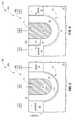
- FIG. 1is a diagrammatic cross-sectional view of a portion of a semiconductor construction illustrating an example embodiment transistor incorporated into an example embodiment memory cell.
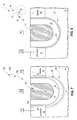
- FIG. 2diagrammatically illustrates the memory cell of FIG. 1 in two different example memory states.
- FIGS. 3-7diagrammatically illustrate example embodiment transistors incorporated into example embodiment memory cells.
- FIG. 8illustrates another embodiment memory cell comprising the example embodiment transistor of FIG. 1 .
- Some embodimentsinclude transistors which comprise ferroelectric material incorporated into gate dielectric. In some embodiments, such transistors may be incorporated into memory cells. Example embodiments are described with reference to FIGS. 1-8 .
- an example embodiment memory cell 40is illustrated as part of a semiconductor construction 10 .
- the construction 10includes a base 12 .
- the base 12may comprise semiconductor material, and in some embodiments may comprise, consist essentially of, or consist of monocrystalline silicon. In some embodiments, base 12 may be considered to comprise a semiconductor substrate.
- semiconductor substratemeans any construction comprising semiconductive material, including, but not limited to, bulk semiconductive materials such as a semiconductive wafer (either alone or in assemblies comprising other materials), and semiconductive material layers (either alone or in assemblies comprising other materials).
- substraterefers to any supporting structure, including, but not limited to, the semiconductor substrates described above.
- base 12may correspond to a semiconductor substrate containing one or more materials associated with integrated circuit fabrication. Some of the materials may be under the shown region of base 12 and/or may be laterally adjacent the shown region of base 12 ; and may correspond to, for example, one or more of refractory metal materials, barrier materials, diffusion materials, insulator materials, etc.
- a transistor gate 14extends into base 12 .
- the transistor gatecomprises gate material 16 .
- Such gate materialmay be any suitable composition or combination of compositions; and in some embodiments may comprise, consist essentially of, or consist of one or more of various metals (for example, tungsten, titanium, etc.), metal-containing compositions (for instance, metal nitride, metal carbide, metal silicide, etc.), and conductively-doped semiconductor materials (for instance, conductively-doped silicon, conductively-doped germanium, etc.).
- the gate material 16may comprise, consist essentially of, or consist of one or more of titanium nitride, titanium aluminum nitride, tungsten nitride, copper and tantalum nitride.
- Gate dielectric 18is between gate material 14 and base 12 .
- the gate dielectricis configured as an upwardly-opening container 24 along the cross-section of FIG. 1 , and the gate 14 is within such container.
- the gate dielectriccomprises two separate materials 20 and 22 in the embodiment of FIG. 1 , which may be referred to as a first material and a second material, respectively.
- the first material 20forms an outer boundary of the container 24 , and is directly against the semiconductor base 12 .
- the second material 22is between the first material 20 and the gate 14 .
- the first material 20is a non-ferroelectric material
- the second materialis a ferroelectric material.
- the first material 20may comprise, consist essentially of, or consist of one or both of silicon dioxide and silicon nitride; and the second material 22 may comprise, consist essentially of, or consist of one or more of yttrium-doped zirconium oxide, yttrium-doped hafnium oxide, magnesium-doped zirconium oxide, magnesium-doped hafnium oxide, silicon-doped hafnium oxide, silicon-doped zirconium oxide and barium-doped titanium oxide.
- the first material 20may comprise one or more of silicon, nitrogen and oxygen; and the second material 22 may comprise one or more of Hf, Zr, Si, O, Y, Ba, Mg and Ti.
- the ferroelectric material 22may have a thickness within a range of from about 10 angstroms to about 200 angstroms, and the non-ferroelectric material 20 may have a thickness within a range of from about 10 angstroms to about 20 angstroms.
- Construction 10comprises a conductively-doped source region 26 extending into base 12 , and a conductively-doped drain region 28 extending into the base. Lower boundaries of the source and drain regions are diagrammatically illustrated with dashed lines.
- the source and drain regionsare both adjacent to gate 14 , and are spaced from the gate by the gate dielectric 18 .
- the source and drain regionsare spaced from one another by a channel region 30 that extends under the gate 14 .
- the source region 26may be referred to as a first region of the base adjacent to the gate 14
- the drain region 28may be referred to as a second region of the base adjacent to the gate.
- Such first and second regions of the baseare spaced from one another by an intervening region of the base comprising the channel region 30 .
- the gate dielectric 18may be considered to comprise a first segment 23 between the source region 26 and the gate 14 , a second segment 25 between the drain region 28 and the gate 14 , and a third segment 27 between the first and second segments.
- the segment 23may be considered to correspond to a first substantially vertical leg of container 24
- the segment 25may be considered to correspond to a second substantially vertical leg of the container
- the segment 27may be considered to comprise a bottom of the container.
- all of the first, second and third segments ( 23 , 25 and 27 ) of gate dielectric 18comprise ferroelectric material 22 .
- the ferroelectric material 22may be omitted from one or more of such segments.
- the non-ferroelectric material 20provides a barrier between ferroelectric material 22 and base 12 to avoid undesired diffusion of constituents between the ferroelectric material and the base and/or to avoid undesired reaction or other interaction between the ferroelectric material and the base.
- the non-ferro electric material 20may be provided entirely along an outer edge of the gate dielectric (as shown) to form a boundary of the container 24 against the semiconductor base 12 (with source and drain regions 26 and 28 being considered to be part of the base).
- diffusion and/or other interactionsare not problematic relative to the ferroelectric material 22 even in the absence of at least some of the non-ferroelectric material, and accordingly some or all the non-ferroelectric material 20 may be omitted from one or more of the segments 23 , 25 and 27 .
- the non-ferroelectric material 20is a substantially consistent thickness along an entirety of container 24 .
- the non-ferroelectric material 20may have a different thickness along one region of container 24 as compared to another region.
- source region 26is electrically coupled to circuitry 32
- drain region 28is electrically coupled to circuitry 34
- gate 14is electrically coupled to circuitry 36 .
- a transistor 38comprises the gate 14 together with the source/drain regions 26 and 28 , and such transistor is incorporated into an integrated circuit through circuitry 32 , 34 and 36 .
- transistor 38may be utilized in other applications.
- transistor 38may be utilized in logic or other circuitry in place of a conventional transistor.
- the ferroelectric material 22 of gate dielectric 18may be polarized into either of two stable orientations, which may enable two selectable states of memory cell 40 .
- Example memory statesare shown in FIG. 2 , with the memory states being labeled as “MEMORY STATE 1” and “MEMORY STATE 2”.
- the illustrated memory cell of FIG. 2has n-type doped source and drain regions 26 and 28 , and a p-type doped channel region. In other embodiments, the source and drain regions may be p-type doped and the channel region may be n-type doped.
- MEMORY STATE 1 and MEMORY STATE 2differ from one another relative to the orientation of charge within ferroelectric material 22 .
- Such charge orientationis diagrammatically illustrated with “+” and “ ⁇ ” in the diagrammatic illustrations of FIG. 2 .
- the memory states of FIG. 2are shown to differ from one another relative to charge polarization within ferroelectric material 22 .
- a double-headed arrow 41is provided in FIG. 2 to diagrammatically illustrate that the memory cell 40 may be reversibly transitioned between the shown memory states.
- the polarization change within ferroelectric material 22specifically occurs within the region 23 between gate 14 and source region 26 (the polarization change may also occur in other regions, such as adjacent the channel in some embodiments; or may occur only in the region 23 as shown in FIG. 2 ).
- the MEMORY STATE 1comprises a “+” component of the polarized ferroelectric material along the n-type doped source region 26
- the MEMORY STATE 2comprises a “ ⁇ ” component of the polarized ferroelectric material along the n-type doped source region 26 .
- the “ ⁇ ” component of the ferroelectric materialis shown to induce a depletion region 42 within the n-type doped source region 26 (a boundary of the depletion region is diagrammatically illustrated with the dashed line 43 ).
- the depletion region 42is deep within the source region 26 , and specifically is along a portion of the source region that interfaces with channel region 30 .
- the transistor 38may have an increased effective channel length relative to an analogous transistor lacking the depletion region, which may reduce short channel effects and thereby improve scalability of the memory cell for higher levels of integration.
- the non-ferroelectric material 20is between ferroelectric material 22 and source region 26 , and accordingly the depletion region 42 is spaced from the ferroelectric material 22 by a segment of non-ferroelectric material 20 .
- the non-ferroelectric material 20may be omitted, and the depletion region 42 may directly contact the ferroelectric material 22 .
- the memory cell 40 of FIG. 2may have advantages of being substantially nonvolatile, and of retaining stored information in the absence of power.
- the memory cell 40may be programmed with any suitable operation, and in some example embodiments may be programmed utilizing voltage differentials between gate 14 and source 26 of less than or equal to about 10 volts; in some example embodiments utilizing voltage differentials of less than or equal to about 5 volts; and in some example embodiments utilizing voltage differentials of from about 0.5 volts to about 5 volts.
- the dopant concentrations utilized within source region 26 and drain region 28may be any suitable dopant concentrations.
- the drain regionmay be more heavily doped than at least some of the source region; and in some embodiments the entirety of the drain region may be more heavily doped than any portion of the source region.
- relatively heavy doping of the drain regionalleviates influence of ferroelectric polarization on operation of the drain side of transistor 38 , while relatively light doping of at least some of the source region enables the influence of the ferroelectric polarization on the source side of the transistor to be enhanced relative to the influence that would occur with heavier doping of the source region.
- the terms “relatively heavy doping” and “relatively light doping”are utilized with reference to one another, and thus the term “relatively heavy doping” means doping heavier than the doping indicated by the term “relatively light doping”.
- the drain region 28may be n-type doped, and some or all of the drain region may comprise a dopant concentration of at least about 1 ⁇ 10 20 atoms/centimeter 3 ; such as, for example, a dopant concentration within a range of from about 1 ⁇ 10 18 atoms/centimeter 3 to about 1 ⁇ 10 20 atoms/centimeter 3 .
- the source region 26may be n-type doped, and at least some of the source region may comprise a dopant concentration of less than about 1 ⁇ 10 20 atoms/centimeter 3 ; such as, for example, a dopant concentration within a range of from about 1 ⁇ 10 16 atoms/centimeter 3 to about 1 ⁇ 10 19.5 atoms/centimeter 3 .
- the source region 26may comprise a gradient of dopant concentration, with dopant concentration being lighter at deeper locations of the source region as compared to shallower locations of the source region.
- FIG. 3shows a construction 10 a illustrating an example embodiment memory cell 40 a having decreasing dopant concentration with increasing depth in the source region, (the dopant concentration is illustrated as [DOPANT]).
- the construction of FIG. 3advantageously may comprise the lighter dopant concentration within the source region at a location where the depletion region 42 forms during programming of a memory state analogous to the MEMORY STATE 2 of FIG. 2 .
- the example embodiment memory cell 40 shown in FIG. 1comprises both ferroelectric material 22 and non-ferroelectric material 20 within all of the segments 23 , 25 and 27 of dielectric material 18 .
- FIG. 4shows an alternative example embodiment memory cell 40 b having ferroelectric material 22 only within segment 23 .
- the memory cell 40 bis part of a construction 10 b , and comprises a transistor 38 b containing gate dielectric 18 b .
- the gate dielectric 18 bcomprises the non-ferroelectric material 20 between ferroelectric material 22 and source region 26 , and comprises additional non-ferroelectric material 50 throughout the segments 25 and 27 (i.e., the segments along drain region 28 and channel region 30 ).
- the non-ferroelectric material 50may comprise any suitable composition or combination of compositions.
- the non-ferroelectric material 50may comprise a same composition as non-ferroelectric material 20 , and in other embodiments may comprise a different composition than non-ferroelectric material 20 .
- non-ferroelectric material 50may comprise, consist essentially of, or consist of one or both of second dioxide and second nitride.
- the memory cell 40 b of FIG. 4like the above-discussed embodiment of FIG. 1 , comprises non-ferroelectric material entirely along an interface of the source region 26 and the gate dielectric, and entirely along an interface of the drain region 28 and the gate dielectric.
- FIG. 5shows a memory cell analogous to that of FIG. 4 , but in which an interface of the gate dielectric with the source region comprises ferroelectric material.
- FIG. 5shows a construction 10 c comprising a memory cell 40 c having a transistor 38 c with gate dielectric 18 c .
- the gate dielectric 18 ccomprises ferroelectric material 22 and non-ferroelectric material 50 .
- the ferroelectric material 22directly contacts both the source region 26 and the gate 14 .
- a portion of the segment of the gate dielectric between the source region and the transistor gatei.e., a portion of the segment 23 of the gate dielectric
- the remainder of the gate dielectrici.e., the remainder segment 23 , together with segments 25 and 27
- a portion of an interface between the gate dielectric 18 c and the source region 26consists of ferroelectric material 22 .
- an entirety of the interface between the gate dielectric and the source regionmay consist of the ferroelectric material.
- FIG. 6shows a construction 10 d illustrating another example embodiment memory cell 40 d .
- the memory cellcomprises a transistor 38 d having gate dielectric 18 d .
- the gate dielectriccomprises non-ferroelectric material 50 throughout the entirety of the segment between the source region 26 and the gate 14 (i.e., the segment 23 ), and throughout the entirety of the segment between the drain region 28 and the gate 14 (i.e., the segment 25 ).
- the gate dielectricfurther comprises ferroelectric material 22 within at least some of the segment along the channel region 30 (i.e., the segment 27 ).
- Suchmay enable selective coupling of the ferroelectric material with the channel region, exclusive of coupling between the ferroelectric material and the source region and/or drain region, which may enable operational characteristics of the memory cell to be tailored for particular applications.
- transistor 38 dis utilized in place of a conventional transistor in an integrated circuit application other than as a part of a memory cell, the selective coupling to the channel region may enable operational aspects of such transistor to be tailored for specific applications.
- FIG. 6shows the non-ferroelectric material 20 provided between ferroelectric material 22 and base 12 .
- the non-ferroelectric material 20may be omitted so that ferroelectric material 22 directly contacts base 12 .
- FIG. 7Another example embodiment memory cell 40 e is shown in FIG. 7 as part of a construction 10 e comprising a transistor 38 e with gate dielectric 18 e .
- the memory cell 40 e of FIG. 7is similar to the memory cell 40 of FIG. 1 , in that the memory cell 40 e comprises both the non-ferroelectric material 20 and the ferroelectric material 22 within all of the segments 23 , 25 and 27 of the gate dielectric.
- that of FIG. 7has the non-ferroelectric material 20 thicker within the segment 27 (i.e. along the bottom of the container 24 defined by the gate dielectric) than within the segments 23 and 25 (i.e., along the substantially vertical legs of the container 24 defined by the gate dielectric).
- the non-ferroelectric material 20may have a thickness within segments 23 and 25 within a range of from about 10 angstroms to about 20 angstroms, and may have a thickness along the bottom of container 24 within a range of from about 25 angstroms to about 50 angstroms.
- the memory cells described abovemay comprise DRAM-type cells.
- the circuitry 34may correspond to a charge-storage device (such as, for example, a capacitor), the circuitry 32 may include an access/sense line (such as, for example, a bitline), and the circuitry 36 may include a wordline that extends in and out of the page relative to the cross-sections of FIGS. 1-7 .
- FIG. 8shows a construction 10 f comprising the transistor 38 of FIG. 1 incorporated into a DRAM-type memory cell 80 .
- the DRAM-type cell of FIG. 8may be, in a sense, considered to include both a volatile memory storage component (the capacitor 70 , with such component storing data by utilizing different charge states of the capacitor as different memory states) and a nonvolatile memory storage component (the transistor 38 , with such component storing data by utilizing different polarization orientations of ferroelectric material 22 as different memory states, as discussed above with reference to FIG. 2 ).
- the volatile memory storage componentmay have rapid read/write characteristics analogous to those of a conventional DRAM, and the nonvolatile memory storage component may enable the cell to have capabilities beyond those of conventional DRAM.
- the cellmay be configured so that the nonvolatile memory storage component backs up information from the volatile memory storage component so that the information is stable in the event of power failure.
- the cellmay be configured so that the nonvolatile memory storage component is utilized for operations separate from those conducted by the volatile memory storage component and/or for operations that modify or overlap those of the volatile memory storage component.
- Suchmay enable a DRAM array comprising memory cells 80 of the type shown in FIG. 8 to perform operations that would otherwise comprise both logic and memory aspects of conventional integrated circuitry, which may enable a DRAM array comprising memory cells 40 of the type shown in FIG. 8 to be scaled to higher levels of integration than may be achieved with conventional DRAM circuitry.
- the devices discussed abovemay be incorporated into electronic systems.
- Such electronic systemsmay be used in, for example, memory modules, device drivers, power modules, communication modems, processor modules, and application-specific modules, and may include multilayer, multichip modules.
- the electronic systemsmay be any of a broad range of systems, such as, for example, clocks, televisions, cell phones, personal computers, automobiles, industrial control systems, aircraft, etc.
- a semiconductor constructionincludes a semiconductor base and a gate extending into the base.
- a first region of the base adjacent the gateis a conductively-doped source region, and a second region of the base adjacent the gate and spaced from the first region is a conductively-doped drain region.
- a gate dielectriccomprises a first segment between the source region and the gate, a second segment between the drain region and the gate, and a third segment between the first and second segments. At least a portion of the gate dielectric comprises ferroelectric material.
- a transistorcomprises a gate, a source region, a drain region, and a channel region between the source and drain regions.
- the transistoralso comprises a gate dielectric between the gate and the source, drain and channel regions.
- the gate dielectriccomprises ferroelectric material between the source region and the gate.
- a semiconductor constructioncomprises a semiconductor base and a gate extending into the base.
- a region of the base on one side of the gateis a conductively-doped source region, and a region of the base on an opposing side of the gate relative to said one side is a conductively-doped drain region.
- the drain regionis more heavily doped than the source region.
- the constructionincludes gate dielectric which comprises a first segment between the source region and the gate, a second segment between the drain region and the gate, and a third segment between the first and second segments.
- the gate dielectric, along a cross-sectionis configured as an upwardly-opening container having the gate therein.
- the first segment of the gate dielectriccomprises a first substantially vertical leg of the container.
- the second segment of the gate dielectriccomprises a second substantially vertical leg of the container.
- the third segment of the gate dielectriccomprises a bottom of the container.
- the gate dielectriccomprises non-ferroelectric material directly against ferroelectric material, with the non-ferroelectric material being a boundary of the container directly against the semiconductor base.
- the non-ferroelectric materialis thicker along the bottom of the container than along the first and second substantially vertical legs of the container.
Landscapes
- Semiconductor Memories (AREA)
- Non-Volatile Memory (AREA)
- Thin Film Transistor (AREA)
Abstract
Description
Claims (22)
Priority Applications (14)
| Application Number | Priority Date | Filing Date | Title |
|---|---|---|---|
| US13/682,190US8796751B2 (en) | 2012-11-20 | 2012-11-20 | Transistors, memory cells and semiconductor constructions |
| JP2015543051AJP6181196B2 (en) | 2012-11-20 | 2013-10-15 | Transistor, memory cell and semiconductor structure |
| EP19215638.8AEP3651198A1 (en) | 2012-11-20 | 2013-10-15 | Transistors and semiconductor constructions |
| CN201810003717.XACN108054213B (en) | 2012-11-20 | 2013-10-15 | Transistors, memory cells, and semiconductor structures |
| PCT/US2013/065102WO2014081518A1 (en) | 2012-11-20 | 2013-10-15 | Transistors, memory cells and semiconductor constructions |
| KR1020157015708AKR101719083B1 (en) | 2012-11-20 | 2013-10-15 | Transistors, memory cells and semiconductor constructions |
| EP13856981.9AEP2923378B1 (en) | 2012-11-20 | 2013-10-15 | Transistors, memory cells and semiconductor constructions |
| CN201380059900.7ACN104798200B (en) | 2012-11-20 | 2013-10-15 | Transistor, memory cell and semiconductor construction |
| TW102138953ATWI512992B (en) | 2012-11-20 | 2013-10-28 | Transistor, memory cell and semiconductor structure |
| US14/331,026US9263672B2 (en) | 2012-11-20 | 2014-07-14 | Transistors, memory cells and semiconductor constructions |
| US14/991,792US9590066B2 (en) | 2012-11-20 | 2016-01-08 | Transistors, memory cells and semiconductor constructions |
| US15/411,886US9882016B2 (en) | 2012-11-20 | 2017-01-20 | Transistors, memory cells and semiconductor constructions |
| US15/859,122US10943986B2 (en) | 2012-11-20 | 2017-12-29 | Transistors, memory cells and semiconductor constructions comprising ferroelectric gate dielectric |
| US17/180,270US11594611B2 (en) | 2012-11-20 | 2021-02-19 | Transistors, memory cells and semiconductor constructions |
Applications Claiming Priority (1)
| Application Number | Priority Date | Filing Date | Title |
|---|---|---|---|
| US13/682,190US8796751B2 (en) | 2012-11-20 | 2012-11-20 | Transistors, memory cells and semiconductor constructions |
Related Child Applications (1)
| Application Number | Title | Priority Date | Filing Date |
|---|---|---|---|
| US14/331,026DivisionUS9263672B2 (en) | 2012-11-20 | 2014-07-14 | Transistors, memory cells and semiconductor constructions |
Publications (2)
| Publication Number | Publication Date |
|---|---|
| US20140138753A1 US20140138753A1 (en) | 2014-05-22 |
| US8796751B2true US8796751B2 (en) | 2014-08-05 |
Family
ID=50727141
Family Applications (6)
| Application Number | Title | Priority Date | Filing Date |
|---|---|---|---|
| US13/682,190ActiveUS8796751B2 (en) | 2012-11-20 | 2012-11-20 | Transistors, memory cells and semiconductor constructions |
| US14/331,026Active2032-12-27US9263672B2 (en) | 2012-11-20 | 2014-07-14 | Transistors, memory cells and semiconductor constructions |
| US14/991,792ActiveUS9590066B2 (en) | 2012-11-20 | 2016-01-08 | Transistors, memory cells and semiconductor constructions |
| US15/411,886ActiveUS9882016B2 (en) | 2012-11-20 | 2017-01-20 | Transistors, memory cells and semiconductor constructions |
| US15/859,122ActiveUS10943986B2 (en) | 2012-11-20 | 2017-12-29 | Transistors, memory cells and semiconductor constructions comprising ferroelectric gate dielectric |
| US17/180,270Active2033-05-01US11594611B2 (en) | 2012-11-20 | 2021-02-19 | Transistors, memory cells and semiconductor constructions |
Family Applications After (5)
| Application Number | Title | Priority Date | Filing Date |
|---|---|---|---|
| US14/331,026Active2032-12-27US9263672B2 (en) | 2012-11-20 | 2014-07-14 | Transistors, memory cells and semiconductor constructions |
| US14/991,792ActiveUS9590066B2 (en) | 2012-11-20 | 2016-01-08 | Transistors, memory cells and semiconductor constructions |
| US15/411,886ActiveUS9882016B2 (en) | 2012-11-20 | 2017-01-20 | Transistors, memory cells and semiconductor constructions |
| US15/859,122ActiveUS10943986B2 (en) | 2012-11-20 | 2017-12-29 | Transistors, memory cells and semiconductor constructions comprising ferroelectric gate dielectric |
| US17/180,270Active2033-05-01US11594611B2 (en) | 2012-11-20 | 2021-02-19 | Transistors, memory cells and semiconductor constructions |
Country Status (7)
| Country | Link |
|---|---|
| US (6) | US8796751B2 (en) |
| EP (2) | EP2923378B1 (en) |
| JP (1) | JP6181196B2 (en) |
| KR (1) | KR101719083B1 (en) |
| CN (2) | CN104798200B (en) |
| TW (1) | TWI512992B (en) |
| WO (1) | WO2014081518A1 (en) |
Cited By (3)
| Publication number | Priority date | Publication date | Assignee | Title |
|---|---|---|---|---|
| US10748931B2 (en) | 2018-05-08 | 2020-08-18 | Micron Technology, Inc. | Integrated assemblies having ferroelectric transistors with body regions coupled to carrier reservoirs |
| US10748914B2 (en) | 2015-12-03 | 2020-08-18 | Micron Technology, Inc. | Ferroelectric capacitor, ferroelectric field effect transistor, and method used in forming an electronic component comprising conductive material and ferroelectric material |
| US11348932B2 (en) | 2019-03-06 | 2022-05-31 | Micron Technology, Inc. | Integrated assemblies having transistor body regions coupled to carrier-sink-structures; and methods of forming integrated assemblies |
Families Citing this family (30)
| Publication number | Priority date | Publication date | Assignee | Title |
|---|---|---|---|---|
| US8796751B2 (en) | 2012-11-20 | 2014-08-05 | Micron Technology, Inc. | Transistors, memory cells and semiconductor constructions |
| US9263577B2 (en) | 2014-04-24 | 2016-02-16 | Micron Technology, Inc. | Ferroelectric field effect transistors, pluralities of ferroelectric field effect transistors arrayed in row lines and column lines, and methods of forming a plurality of ferroelectric field effect transistors |
| US9472560B2 (en) | 2014-06-16 | 2016-10-18 | Micron Technology, Inc. | Memory cell and an array of memory cells |
| US9159829B1 (en) | 2014-10-07 | 2015-10-13 | Micron Technology, Inc. | Recessed transistors containing ferroelectric material |
| US9305929B1 (en) | 2015-02-17 | 2016-04-05 | Micron Technology, Inc. | Memory cells |
| KR102295641B1 (en)* | 2015-03-02 | 2021-08-27 | 삼성전자주식회사 | Semiconductor device and manufacturing the same |
| US10134982B2 (en) | 2015-07-24 | 2018-11-20 | Micron Technology, Inc. | Array of cross point memory cells |
| US9853211B2 (en) | 2015-07-24 | 2017-12-26 | Micron Technology, Inc. | Array of cross point memory cells individually comprising a select device and a programmable device |
| KR102616134B1 (en)* | 2016-02-26 | 2023-12-21 | 에스케이하이닉스 주식회사 | Non-volatile Memory Device Including Ferroelectric And Method of Manufacturing The Same |
| KR102616129B1 (en)* | 2016-02-26 | 2023-12-21 | 에스케이하이닉스 주식회사 | Multi-level Ferroelectric Memory Device And Method of Manufacturing The Same |
| KR102166238B1 (en)* | 2016-04-01 | 2020-10-15 | 인텔 코포레이션 | Ferroelectric based field effect transistor with threshold voltage switching for enhanced on-state and off-state performance |
| KR102686060B1 (en) | 2016-10-26 | 2024-07-17 | 에스케이하이닉스 주식회사 | Nonvolatile Memory Device and Method of Writing Nonvolatile Memory Device |
| US10396145B2 (en) | 2017-01-12 | 2019-08-27 | Micron Technology, Inc. | Memory cells comprising ferroelectric material and including current leakage paths having different total resistances |
| KR20180106661A (en)* | 2017-03-21 | 2018-10-01 | 에스케이하이닉스 주식회사 | Ferroelectric memory device and method of fabricating the same |
| US11004868B2 (en) | 2017-03-22 | 2021-05-11 | Intel Corporation | Memory field-effect transistors and methods of manufacturing the same |
| US10790366B2 (en)* | 2018-01-24 | 2020-09-29 | Globalfoundries Singapore Pte. Ltd. | Devices with lower resistance and improved breakdown and method for producing the same |
| KR102494684B1 (en)* | 2018-05-10 | 2023-02-02 | 에스케이하이닉스 주식회사 | Ferroelectric Semiconductor Device and Method of Manufacturing the same |
| US11004867B2 (en)* | 2018-06-28 | 2021-05-11 | Taiwan Semiconductor Manufacturing Co., Ltd. | Embedded ferroelectric memory in high-k first technology |
| US11469323B2 (en) | 2018-09-25 | 2022-10-11 | Intel Corporation | Ferroelectric gate stack for band-to-band tunneling reduction |
| KR102751739B1 (en)* | 2019-06-24 | 2025-01-09 | 삼성전자주식회사 | A semiconductor device |
| US11170834B2 (en) | 2019-07-10 | 2021-11-09 | Micron Technology, Inc. | Memory cells and methods of forming a capacitor including current leakage paths having different total resistances |
| US11171206B2 (en)* | 2019-07-11 | 2021-11-09 | Micron Technology, Inc. | Channel conduction in semiconductor devices |
| US20230369488A1 (en) | 2019-07-24 | 2023-11-16 | Nanya Technology Corporation | Semiconductor memory structure having drain stressor, source stressor and buried gate and method of manufacturing the same |
| US11211491B2 (en)* | 2019-07-24 | 2021-12-28 | Nanya Technology Corporation | Semiconductor memory structure having drain stressor, source stressor and buried gate and method of manufacturing the same |
| KR102681259B1 (en)* | 2019-08-06 | 2024-07-03 | 에스케이하이닉스 주식회사 | Ferroelectric Memory Device having Ferroelectric Induction Layer |
| US11791383B2 (en)* | 2021-07-28 | 2023-10-17 | Infineon Technologies Ag | Semiconductor device having a ferroelectric gate stack |
| US12068390B2 (en) | 2021-07-28 | 2024-08-20 | Infineon Technologies Ag | Power semiconductor device having a gate dielectric stack that includes a ferroelectric insulator |
| US11929411B2 (en) | 2021-08-25 | 2024-03-12 | Micron Technology, Inc. | Recessed access devices and methods of forming a recessed access devices |
| US20230062092A1 (en)* | 2021-08-30 | 2023-03-02 | Micron Technology, Inc. | Recessed Access Devices And Methods Of Forming A Recessed Access Devices |
| US12396176B2 (en)* | 2022-01-24 | 2025-08-19 | Taiwan Semiconductor Manufacturing Company, Ltd. | 3T memory with enhanced speed of operation and data retention |
Citations (14)
| Publication number | Priority date | Publication date | Assignee | Title |
|---|---|---|---|---|
| US5757042A (en) | 1996-06-14 | 1998-05-26 | Radiant Technologies, Inc. | High density ferroelectric memory with increased channel modulation and double word ferroelectric memory cell for constructing the same |
| US6069381A (en) | 1997-09-15 | 2000-05-30 | International Business Machines Corporation | Ferroelectric memory transistor with resistively coupled floating gate |
| US20020061604A1 (en) | 2000-10-26 | 2002-05-23 | Arkalgud Sitaram | Method for fabricating a ferroelectric or paraelectric metal oxide-containing layer and a memory component therefrom |
| US20030107088A1 (en)* | 1997-06-30 | 2003-06-12 | Kabushiki Kaisha Toshiba | Semiconductor device and manufacturing method therefor |
| US6979846B2 (en) | 2002-05-13 | 2005-12-27 | Kabushiki Kaisha Toshiba | Semiconductor device and manufacturing method thereof |
| US7132300B2 (en) | 2003-06-30 | 2006-11-07 | Matsushita Electric Industrial Co., Ltd. | Method for forming ferroelectric film and semiconductor device |
| KR100680978B1 (en) | 2006-05-04 | 2007-02-09 | 주식회사 하이닉스반도체 | Ferroelectric Ram Device |
| US20070272960A1 (en) | 2003-09-09 | 2007-11-29 | Sharp Laboratories Of America, Inc. | Ferroelectric memory transistor with conductive oxide gate structure |
| US20080203443A1 (en)* | 2007-02-22 | 2008-08-28 | American Semiconductor, Inc. | Independently-Double-Gated Transistor Memory (IDGM) |
| US20090261395A1 (en) | 2008-04-21 | 2009-10-22 | Qimonda Ag | Integrated Circuit Including a Ferroelectric Memory Cell and Method of Manufacturing the Same |
| US7960779B2 (en) | 2008-02-28 | 2011-06-14 | Kabushiki Kaisha Toshiba | Nonvolatile semiconductor memory and manufacturing method thereof |
| US20110297927A1 (en) | 2010-06-04 | 2011-12-08 | Micron Technology, Inc. | Oxide based memory |
| US8097911B2 (en) | 2008-12-31 | 2012-01-17 | Intel Corporation | Etch stop structures for floating gate devices |
| US20120033478A1 (en) | 2010-08-05 | 2012-02-09 | Hynix Semiconductor Inc. | Non-volatile memory device and sensing method for forming the same |
Family Cites Families (98)
| Publication number | Priority date | Publication date | Assignee | Title |
|---|---|---|---|---|
| US4243997A (en)* | 1976-03-25 | 1981-01-06 | Tokyo Shibaura Electric Co., Ltd. | Semiconductor device |
| US4724674A (en) | 1985-10-30 | 1988-02-16 | Allied Corporation | Hydraulic brake booster |
| JPH0687500B2 (en)* | 1987-03-26 | 1994-11-02 | 日本電気株式会社 | Semiconductor memory device and manufacturing method thereof |
| US5225363A (en)* | 1988-06-28 | 1993-07-06 | Texas Instruments Incorporated | Trench capacitor DRAM cell and method of manufacture |
| TW199237B (en)* | 1990-07-03 | 1993-02-01 | Siemens Ag | |
| JPH0799310B2 (en) | 1990-12-06 | 1995-10-25 | 品川白煉瓦株式会社 | How to install anchor bricks |
| WO1992012518A1 (en)* | 1991-01-09 | 1992-07-23 | Siemens Aktiengesellschaft | Storage cell arrangement and process for operating it |
| JP3130353B2 (en) | 1991-12-20 | 2001-01-31 | ローム株式会社 | Method of manufacturing device using ferroelectric film |
| JP3098629B2 (en)* | 1992-09-18 | 2000-10-16 | 株式会社日立製作所 | Ferroelectric transistor, semiconductor storage device using the same, semiconductor applied equipment, and artificial intelligence system |
| JP2734961B2 (en)* | 1993-05-24 | 1998-04-02 | 日本電気株式会社 | Field effect transistor and manufacturing method thereof |
| US5589814A (en) | 1994-11-14 | 1996-12-31 | Smith, Jr.; John | Anti-theft vehicle security system |
| JPH0955495A (en)* | 1995-08-14 | 1997-02-25 | Sony Corp | Transistor and its manufacture |
| JPH10189966A (en) | 1996-12-26 | 1998-07-21 | Toshiba Corp | Semiconductor device and manufacturing method thereof |
| JPH10313097A (en)* | 1997-05-13 | 1998-11-24 | Sharp Corp | Ferroelectric thin film, manufacturing method and device comprising ferroelectric thin film |
| DE19720193C2 (en)* | 1997-05-14 | 2002-10-17 | Infineon Technologies Ag | Integrated circuit arrangement with at least two vertical MOS transistors and method for their production |
| JPH1140683A (en)* | 1997-07-22 | 1999-02-12 | Hitachi Ltd | Semiconductor memory device and method of manufacturing the same |
| JPH1168105A (en) | 1997-08-26 | 1999-03-09 | Mitsubishi Electric Corp | Semiconductor device |
| JPH1168104A (en)* | 1997-08-26 | 1999-03-09 | Oki Electric Ind Co Ltd | Field effect transistor and method of manufacturing the same |
| JP3544833B2 (en)* | 1997-09-18 | 2004-07-21 | 株式会社東芝 | Semiconductor device and manufacturing method thereof |
| JP2000012708A (en)* | 1998-06-17 | 2000-01-14 | Toshiba Corp | Semiconductor device and manufacturing method thereof |
| JP3809035B2 (en)* | 1998-06-29 | 2006-08-16 | 株式会社東芝 | MIS type transistor and manufacturing method thereof |
| US6278165B1 (en) | 1998-06-29 | 2001-08-21 | Kabushiki Kaisha Toshiba | MIS transistor having a large driving current and method for producing the same |
| JP3223885B2 (en)* | 1998-08-17 | 2001-10-29 | 日本電気株式会社 | Field effect type semiconductor memory device and method of manufacturing the same |
| JP2000252372A (en)* | 1999-02-26 | 2000-09-14 | Sharp Corp | Semiconductor memory device and method of manufacturing the same |
| US6323580B1 (en)* | 1999-04-28 | 2001-11-27 | The Charles Stark Draper Laboratory, Inc. | Ferroic transducer |
| US7084456B2 (en)* | 1999-05-25 | 2006-08-01 | Advanced Analogic Technologies, Inc. | Trench MOSFET with recessed clamping diode using graded doping |
| US6313033B1 (en)* | 1999-07-27 | 2001-11-06 | Applied Materials, Inc. | Ionized metal plasma Ta, TaNx, W, and WNx liners for gate electrode applications |
| US6159782A (en)* | 1999-08-05 | 2000-12-12 | Advanced Micro Devices, Inc. | Fabrication of field effect transistors having dual gates with gate dielectrics of high dielectric constant |
| JP2001102465A (en)* | 1999-09-30 | 2001-04-13 | Rohm Co Ltd | Non-volatile memory |
| US7227210B2 (en)* | 1999-12-27 | 2007-06-05 | Hynix Semiconductor, Inc. | Ferroelectric memory transistor with highly-oriented film on gate insulator |
| US6642577B2 (en)* | 2000-03-16 | 2003-11-04 | Denso Corporation | Semiconductor device including power MOSFET and peripheral device and method for manufacturing the same |
| JP4938921B2 (en)* | 2000-03-16 | 2012-05-23 | 康夫 垂井 | Transistor-type ferroelectric nonvolatile memory element |
| KR20020015761A (en)* | 2000-08-23 | 2002-03-02 | 김지영 | MeFIS-FET Memory Device and Method of Manufacturing the Same Using Nitride Teatment |
| JP2002110932A (en)* | 2000-09-28 | 2002-04-12 | Toshiba Corp | Semiconductor device and manufacturing method thereof |
| US6555872B1 (en)* | 2000-11-22 | 2003-04-29 | Thunderbird Technologies, Inc. | Trench gate fermi-threshold field effect transistors |
| JP3808702B2 (en)* | 2000-12-28 | 2006-08-16 | 株式会社東芝 | Manufacturing method of semiconductor device |
| JP4895430B2 (en)* | 2001-03-22 | 2012-03-14 | ルネサスエレクトロニクス株式会社 | Semiconductor device and manufacturing method of semiconductor device |
| US6452229B1 (en)* | 2002-02-21 | 2002-09-17 | Advanced Micro Devices, Inc. | Ultra-thin fully depleted SOI device with T-shaped gate and method of fabrication |
| US6815297B1 (en)* | 2002-02-21 | 2004-11-09 | Advanced Micro Devices, Inc. | Ultra-thin fully depleted SOI device and method of fabrication |
| US20040041214A1 (en) | 2002-08-29 | 2004-03-04 | Prall Kirk D. | One F2 memory cell, memory array, related devices and methods |
| CN100407427C (en)* | 2002-06-21 | 2008-07-30 | 微米技术股份有限公司 | NROM memory element, memory array, related apparatus and method |
| US20030235076A1 (en)* | 2002-06-21 | 2003-12-25 | Micron Technology, Inc. | Multistate NROM having a storage density much greater than 1 Bit per 1F2 |
| JP4080816B2 (en)* | 2002-08-13 | 2008-04-23 | 株式会社東芝 | Method for manufacturing field effect transistor |
| US6714435B1 (en)* | 2002-09-19 | 2004-03-30 | Cova Technologies, Inc. | Ferroelectric transistor for storing two data bits |
| DE10306315B4 (en)* | 2003-02-14 | 2007-12-20 | Qimonda Ag | Semiconductor device and corresponding manufacturing method |
| JP2004335918A (en)* | 2003-05-12 | 2004-11-25 | Toshiba Corp | Semiconductor memory device and method of manufacturing the same |
| KR100505713B1 (en)* | 2003-10-22 | 2005-08-03 | 삼성전자주식회사 | Shallow trench isolation and method for forming the same |
| JP2005174977A (en)* | 2003-12-08 | 2005-06-30 | Toshiba Corp | Ferroelectric memory device and manufacturing method thereof |
| US7301804B2 (en) | 2003-12-16 | 2007-11-27 | Micro Technology, Inc. | NROM memory cell, memory array, related devices and methods |
| US7050330B2 (en) | 2003-12-16 | 2006-05-23 | Micron Technology, Inc. | Multi-state NROM device |
| JP2006049566A (en)* | 2004-08-04 | 2006-02-16 | Toshiba Corp | Semiconductor memory device and manufacturing method thereof |
| US7795094B2 (en)* | 2004-09-02 | 2010-09-14 | Micron Technology, Inc. | Recessed gate dielectric antifuse |
| KR100634266B1 (en)* | 2004-09-02 | 2006-10-13 | 삼성전자주식회사 | Nonvolatile memory device, method for manufacturing same and method for operating same |
| KR100621563B1 (en)* | 2004-11-03 | 2006-09-19 | 삼성전자주식회사 | Nonvolatile Memory Device and Manufacturing Method Thereof |
| US7241691B2 (en)* | 2005-03-28 | 2007-07-10 | Freescale Semiconductor, Inc. | Conducting metal oxide with additive as p-MOS device electrode |
| JP4361517B2 (en)* | 2005-06-23 | 2009-11-11 | パナソニック株式会社 | Semiconductor device and manufacturing method thereof |
| US8338887B2 (en) | 2005-07-06 | 2012-12-25 | Infineon Technologies Ag | Buried gate transistor |
| US7202535B2 (en)* | 2005-07-14 | 2007-04-10 | Infineon Technologies Ag | Manufacturing method for an integrated semiconductor structure and corresponding integrated semiconductor structure |
| KR100729231B1 (en)* | 2005-08-03 | 2007-06-15 | 삼성전자주식회사 | Ferroelectric structure, method of forming ferroelectric structure, semiconductor device having ferroelectric structure and manufacturing method thereof |
| US7867845B2 (en)* | 2005-09-01 | 2011-01-11 | Micron Technology, Inc. | Transistor gate forming methods and transistor structures |
| US20070082454A1 (en) | 2005-10-12 | 2007-04-12 | Infineon Technologies Ag | Microelectronic device and method of manufacturing a microelectronic device |
| US7696574B2 (en)* | 2005-10-26 | 2010-04-13 | International Business Machines Corporation | Semiconductor substrate with multiple crystallographic orientations |
| KR100801729B1 (en)* | 2005-11-25 | 2008-02-11 | 주식회사 하이닉스반도체 | Transistor having recessed gate structure and manufacturing method |
| JP4775849B2 (en)* | 2006-01-13 | 2011-09-21 | 富士通セミコンダクター株式会社 | SEMICONDUCTOR ELEMENT, SEMICONDUCTOR MEMORY DEVICE USING SAME, DATA WRITE METHOD, DATA READ METHOD, AND MANUFACTURING METHOD THEREOF |
| DE102006004405B4 (en)* | 2006-01-31 | 2015-05-13 | Infineon Technologies Austria Ag | Power semiconductor components with a drift path and a high-dielectric compensation zone and method for producing a compensation zone |
| JP2007266474A (en)* | 2006-03-29 | 2007-10-11 | Hitachi Ltd | Semiconductor memory device |
| JP2008027955A (en)* | 2006-07-18 | 2008-02-07 | Toshiba Corp | Semiconductor device |
| KR100783278B1 (en)* | 2006-08-31 | 2007-12-06 | 동부일렉트로닉스 주식회사 | Semiconductor device and manufacturing method |
| US8736151B2 (en)* | 2006-09-26 | 2014-05-27 | Velos Industries, LLC | Electric generator |
| JP2008085178A (en)* | 2006-09-28 | 2008-04-10 | Toshiba Corp | Semiconductor device and manufacturing method thereof |
| US7682891B2 (en)* | 2006-12-28 | 2010-03-23 | Intel Corporation | Tunable gate electrode work function material for transistor applications |
| JP4552973B2 (en)* | 2007-06-08 | 2010-09-29 | セイコーエプソン株式会社 | Manufacturing method of semiconductor device |
| KR20090009561A (en)* | 2007-07-20 | 2009-01-23 | 삼성전자주식회사 | Semiconductor device and manufacturing method thereof |
| KR20090009561U (en) | 2008-03-19 | 2009-09-23 | 김우석 | Industrial hose |
| US7875919B2 (en)* | 2008-03-31 | 2011-01-25 | International Business Machines Corporation | Shallow trench capacitor compatible with high-K / metal gate |
| US7936009B2 (en)* | 2008-07-09 | 2011-05-03 | Fairchild Semiconductor Corporation | Shielded gate trench FET with an inter-electrode dielectric having a low-k dielectric therein |
| US7911028B2 (en)* | 2008-07-31 | 2011-03-22 | Nanya Technology Corp. | Semiconductor device and method of manufacturing the same |
| US8003507B2 (en)* | 2008-08-18 | 2011-08-23 | Taiwan Semiconductor Manufacturing Company, Ltd. | Method of integrating high-K/metal gate in CMOS process flow |
| US8105931B2 (en)* | 2008-08-27 | 2012-01-31 | Taiwan Semiconductor Manufacturing Company, Ltd. | Method of fabricating dual high-k metal gates for MOS devices |
| US20100110753A1 (en)* | 2008-10-31 | 2010-05-06 | Qimonda Ag | Ferroelectric Memory Cell Arrays and Method of Operating the Same |
| KR101584097B1 (en) | 2009-03-23 | 2016-01-12 | 삼성전자주식회사 | Method for formation of buried gate electrode |
| JP2011014838A (en)* | 2009-07-06 | 2011-01-20 | Toshiba Corp | Non-volatile semiconductor memory device |
| DE102009038710B4 (en)* | 2009-08-25 | 2020-02-27 | Infineon Technologies Austria Ag | Semiconductor device |
| JP5537555B2 (en)* | 2009-09-29 | 2014-07-02 | 株式会社東芝 | Semiconductor device |
| WO2011075955A1 (en)* | 2009-12-24 | 2011-06-30 | 复旦大学 | Microelectronic device structure and manufacturing method thereof |
| KR101662282B1 (en)* | 2010-01-14 | 2016-10-05 | 삼성전자주식회사 | Semiconductor device having a buried gate pattern including high-k dielectric capping layer and fabricating method thereof |
| JP2011155071A (en)* | 2010-01-26 | 2011-08-11 | Toshiba Corp | Semiconductor memory device |
| JP2011159756A (en)* | 2010-01-29 | 2011-08-18 | Sony Corp | Solid-state imaging device, method of manufacturing the same, and electronic apparatus |
| US20120028425A1 (en)* | 2010-08-02 | 2012-02-02 | Hamilton Lu | Methods for fabricating trench metal oxide semiconductor field effect transistors |
| JP2012060063A (en)* | 2010-09-13 | 2012-03-22 | Toshiba Corp | Semiconductor device and method of manufacturing the same |
| JP2012174866A (en) | 2011-02-21 | 2012-09-10 | Elpida Memory Inc | Semiconductor device and manufacturing method of the same |
| TWI501601B (en) | 2011-08-15 | 2015-09-21 | Mediatek Inc | Device search processing method |
| US9177870B2 (en)* | 2011-12-16 | 2015-11-03 | Taiwan Semiconductor Manufacturing Company Ltd. | Enhanced gate replacement process for high-K metal gate technology |
| WO2013095643A1 (en)* | 2011-12-23 | 2013-06-27 | Intel Corporation | Iii-n material structure for gate-recessed transistors |
| US8823059B2 (en)* | 2012-09-27 | 2014-09-02 | Intel Corporation | Non-planar semiconductor device having group III-V material active region with multi-dielectric gate stack |
| US8796751B2 (en) | 2012-11-20 | 2014-08-05 | Micron Technology, Inc. | Transistors, memory cells and semiconductor constructions |
| KR102686060B1 (en)* | 2016-10-26 | 2024-07-17 | 에스케이하이닉스 주식회사 | Nonvolatile Memory Device and Method of Writing Nonvolatile Memory Device |
| KR20180106661A (en)* | 2017-03-21 | 2018-10-01 | 에스케이하이닉스 주식회사 | Ferroelectric memory device and method of fabricating the same |
- 2012
- 2012-11-20USUS13/682,190patent/US8796751B2/enactiveActive
- 2013
- 2013-10-15EPEP13856981.9Apatent/EP2923378B1/enactiveActive
- 2013-10-15JPJP2015543051Apatent/JP6181196B2/enactiveActive
- 2013-10-15CNCN201380059900.7Apatent/CN104798200B/enactiveActive
- 2013-10-15CNCN201810003717.XApatent/CN108054213B/enactiveActive
- 2013-10-15KRKR1020157015708Apatent/KR101719083B1/enactiveActive
- 2013-10-15WOPCT/US2013/065102patent/WO2014081518A1/enactiveApplication Filing
- 2013-10-15EPEP19215638.8Apatent/EP3651198A1/enactivePending
- 2013-10-28TWTW102138953Apatent/TWI512992B/enactive
- 2014
- 2014-07-14USUS14/331,026patent/US9263672B2/enactiveActive
- 2016
- 2016-01-08USUS14/991,792patent/US9590066B2/enactiveActive
- 2017
- 2017-01-20USUS15/411,886patent/US9882016B2/enactiveActive
- 2017-12-29USUS15/859,122patent/US10943986B2/enactiveActive
- 2021
- 2021-02-19USUS17/180,270patent/US11594611B2/enactiveActive
Patent Citations (15)
| Publication number | Priority date | Publication date | Assignee | Title |
|---|---|---|---|---|
| US5757042A (en) | 1996-06-14 | 1998-05-26 | Radiant Technologies, Inc. | High density ferroelectric memory with increased channel modulation and double word ferroelectric memory cell for constructing the same |
| US20030107088A1 (en)* | 1997-06-30 | 2003-06-12 | Kabushiki Kaisha Toshiba | Semiconductor device and manufacturing method therefor |
| US6664592B2 (en) | 1997-06-30 | 2003-12-16 | Kabushiki Kaisha Toshiba | Semiconductor device with groove type channel structure |
| US6069381A (en) | 1997-09-15 | 2000-05-30 | International Business Machines Corporation | Ferroelectric memory transistor with resistively coupled floating gate |
| US20020061604A1 (en) | 2000-10-26 | 2002-05-23 | Arkalgud Sitaram | Method for fabricating a ferroelectric or paraelectric metal oxide-containing layer and a memory component therefrom |
| US6979846B2 (en) | 2002-05-13 | 2005-12-27 | Kabushiki Kaisha Toshiba | Semiconductor device and manufacturing method thereof |
| US7132300B2 (en) | 2003-06-30 | 2006-11-07 | Matsushita Electric Industrial Co., Ltd. | Method for forming ferroelectric film and semiconductor device |
| US20070272960A1 (en) | 2003-09-09 | 2007-11-29 | Sharp Laboratories Of America, Inc. | Ferroelectric memory transistor with conductive oxide gate structure |
| KR100680978B1 (en) | 2006-05-04 | 2007-02-09 | 주식회사 하이닉스반도체 | Ferroelectric Ram Device |
| US20080203443A1 (en)* | 2007-02-22 | 2008-08-28 | American Semiconductor, Inc. | Independently-Double-Gated Transistor Memory (IDGM) |
| US7960779B2 (en) | 2008-02-28 | 2011-06-14 | Kabushiki Kaisha Toshiba | Nonvolatile semiconductor memory and manufacturing method thereof |
| US20090261395A1 (en) | 2008-04-21 | 2009-10-22 | Qimonda Ag | Integrated Circuit Including a Ferroelectric Memory Cell and Method of Manufacturing the Same |
| US8097911B2 (en) | 2008-12-31 | 2012-01-17 | Intel Corporation | Etch stop structures for floating gate devices |
| US20110297927A1 (en) | 2010-06-04 | 2011-12-08 | Micron Technology, Inc. | Oxide based memory |
| US20120033478A1 (en) | 2010-08-05 | 2012-02-09 | Hynix Semiconductor Inc. | Non-volatile memory device and sensing method for forming the same |
Cited By (8)
| Publication number | Priority date | Publication date | Assignee | Title |
|---|---|---|---|---|
| US10748914B2 (en) | 2015-12-03 | 2020-08-18 | Micron Technology, Inc. | Ferroelectric capacitor, ferroelectric field effect transistor, and method used in forming an electronic component comprising conductive material and ferroelectric material |
| US11552086B2 (en) | 2015-12-03 | 2023-01-10 | Micron Technology, Inc. | Ferroelectric capacitor, ferroelectric field effect transistor, and method used in forming an electronic component comprising conductive material and ferroelectric material |
| US11856790B2 (en) | 2015-12-03 | 2023-12-26 | Micron Technology, Inc. | Ferroelectric capacitors |
| US10748931B2 (en) | 2018-05-08 | 2020-08-18 | Micron Technology, Inc. | Integrated assemblies having ferroelectric transistors with body regions coupled to carrier reservoirs |
| US11469250B2 (en) | 2018-05-08 | 2022-10-11 | Micron Technology, Inc. | Integrated assemblies having ferroelectric transistors with body regions coupled to carrier reservoirs; and methods of forming integrated assemblies |
| US11348932B2 (en) | 2019-03-06 | 2022-05-31 | Micron Technology, Inc. | Integrated assemblies having transistor body regions coupled to carrier-sink-structures; and methods of forming integrated assemblies |
| US11910597B2 (en) | 2019-03-06 | 2024-02-20 | Micron Technology, Inc. | Integrated assemblies having transistor body regions coupled to carrier-sink-structures; and methods of forming integrated assemblies |
| US12219758B2 (en) | 2019-03-06 | 2025-02-04 | Micron Technology, Inc. | Integrated assemblies having transistor body regions coupled to carrier-sink-structures; and methods of forming integrated assemblies |
Also Published As
| Publication number | Publication date |
|---|---|
| US11594611B2 (en) | 2023-02-28 |
| CN108054213A (en) | 2018-05-18 |
| JP6181196B2 (en) | 2017-08-16 |
| US9882016B2 (en) | 2018-01-30 |
| CN108054213B (en) | 2021-07-09 |
| WO2014081518A1 (en) | 2014-05-30 |
| EP2923378B1 (en) | 2020-01-22 |
| EP2923378A4 (en) | 2016-08-24 |
| US9263672B2 (en) | 2016-02-16 |
| TWI512992B (en) | 2015-12-11 |
| US10943986B2 (en) | 2021-03-09 |
| TW201428971A (en) | 2014-07-16 |
| US20160133717A1 (en) | 2016-05-12 |
| US9590066B2 (en) | 2017-03-07 |
| EP3651198A1 (en) | 2020-05-13 |
| US20210175340A1 (en) | 2021-06-10 |
| EP2923378A1 (en) | 2015-09-30 |
| CN104798200B (en) | 2018-02-02 |
| KR101719083B1 (en) | 2017-03-22 |
| US20140138753A1 (en) | 2014-05-22 |
| US20180122917A1 (en) | 2018-05-03 |
| CN104798200A (en) | 2015-07-22 |
| JP2015535146A (en) | 2015-12-07 |
| KR20150082629A (en) | 2015-07-15 |
| US20140332750A1 (en) | 2014-11-13 |
| US20170133478A1 (en) | 2017-05-11 |
Similar Documents
| Publication | Publication Date | Title |
|---|---|---|
| US11594611B2 (en) | Transistors, memory cells and semiconductor constructions | |
| US12223994B2 (en) | Memory arrays, ferroelectric transistors, and methods of reading and writing relative to memory cells of memory arrays | |
| US11715797B2 (en) | Ferroelectric transistors and assemblies comprising ferroelectric transistors | |
| US10553595B2 (en) | Memory cell and an array of memory cells | |
| US9159829B1 (en) | Recessed transistors containing ferroelectric material | |
| US10056386B2 (en) | Memory cells and memory arrays | |
| US20210242221A1 (en) | Integrated Assemblies Having Ferroelectric Transistors with Heterostructure Active Regions | |
| US11515331B2 (en) | Integrated assemblies comprising ferroelectric transistors and non-ferroelectric transistors | |
| US9059030B2 (en) | Memory cells having capacitor dielectric directly against a transistor source/drain region |
Legal Events
| Date | Code | Title | Description |
|---|---|---|---|
| AS | Assignment | Owner name:MICRON TECHNOLOGY, INC., IDAHO Free format text:ASSIGNMENT OF ASSIGNORS INTEREST;ASSIGNORS:RAMASWAMY, NIRMAL;PRALL, KIRK D.;KINNEY, WAYNE;SIGNING DATES FROM 20121114 TO 20121119;REEL/FRAME:029332/0119 | |
| FEPP | Fee payment procedure | Free format text:PAYOR NUMBER ASSIGNED (ORIGINAL EVENT CODE: ASPN); ENTITY STATUS OF PATENT OWNER: LARGE ENTITY | |
| STCF | Information on status: patent grant | Free format text:PATENTED CASE | |
| AS | Assignment | Owner name:U.S. BANK NATIONAL ASSOCIATION, AS COLLATERAL AGENT, CALIFORNIA Free format text:SECURITY INTEREST;ASSIGNOR:MICRON TECHNOLOGY, INC.;REEL/FRAME:038669/0001 Effective date:20160426 Owner name:U.S. BANK NATIONAL ASSOCIATION, AS COLLATERAL AGEN Free format text:SECURITY INTEREST;ASSIGNOR:MICRON TECHNOLOGY, INC.;REEL/FRAME:038669/0001 Effective date:20160426 | |
| AS | Assignment | Owner name:MORGAN STANLEY SENIOR FUNDING, INC., AS COLLATERAL AGENT, MARYLAND Free format text:PATENT SECURITY AGREEMENT;ASSIGNOR:MICRON TECHNOLOGY, INC.;REEL/FRAME:038954/0001 Effective date:20160426 Owner name:MORGAN STANLEY SENIOR FUNDING, INC., AS COLLATERAL Free format text:PATENT SECURITY AGREEMENT;ASSIGNOR:MICRON TECHNOLOGY, INC.;REEL/FRAME:038954/0001 Effective date:20160426 | |
| AS | Assignment | Owner name:U.S. BANK NATIONAL ASSOCIATION, AS COLLATERAL AGENT, CALIFORNIA Free format text:CORRECTIVE ASSIGNMENT TO CORRECT THE REPLACE ERRONEOUSLY FILED PATENT #7358718 WITH THE CORRECT PATENT #7358178 PREVIOUSLY RECORDED ON REEL 038669 FRAME 0001. ASSIGNOR(S) HEREBY CONFIRMS THE SECURITY INTEREST;ASSIGNOR:MICRON TECHNOLOGY, INC.;REEL/FRAME:043079/0001 Effective date:20160426 Owner name:U.S. BANK NATIONAL ASSOCIATION, AS COLLATERAL AGEN Free format text:CORRECTIVE ASSIGNMENT TO CORRECT THE REPLACE ERRONEOUSLY FILED PATENT #7358718 WITH THE CORRECT PATENT #7358178 PREVIOUSLY RECORDED ON REEL 038669 FRAME 0001. ASSIGNOR(S) HEREBY CONFIRMS THE SECURITY INTEREST;ASSIGNOR:MICRON TECHNOLOGY, INC.;REEL/FRAME:043079/0001 Effective date:20160426 | |
| MAFP | Maintenance fee payment | Free format text:PAYMENT OF MAINTENANCE FEE, 4TH YEAR, LARGE ENTITY (ORIGINAL EVENT CODE: M1551) Year of fee payment:4 | |
| AS | Assignment | Owner name:JPMORGAN CHASE BANK, N.A., AS COLLATERAL AGENT, ILLINOIS Free format text:SECURITY INTEREST;ASSIGNORS:MICRON TECHNOLOGY, INC.;MICRON SEMICONDUCTOR PRODUCTS, INC.;REEL/FRAME:047540/0001 Effective date:20180703 Owner name:JPMORGAN CHASE BANK, N.A., AS COLLATERAL AGENT, IL Free format text:SECURITY INTEREST;ASSIGNORS:MICRON TECHNOLOGY, INC.;MICRON SEMICONDUCTOR PRODUCTS, INC.;REEL/FRAME:047540/0001 Effective date:20180703 | |
| AS | Assignment | Owner name:MICRON TECHNOLOGY, INC., IDAHO Free format text:RELEASE BY SECURED PARTY;ASSIGNOR:U.S. BANK NATIONAL ASSOCIATION, AS COLLATERAL AGENT;REEL/FRAME:047243/0001 Effective date:20180629 | |
| AS | Assignment | Owner name:MICRON TECHNOLOGY, INC., IDAHO Free format text:RELEASE BY SECURED PARTY;ASSIGNOR:MORGAN STANLEY SENIOR FUNDING, INC., AS COLLATERAL AGENT;REEL/FRAME:050937/0001 Effective date:20190731 | |
| AS | Assignment | Owner name:MICRON TECHNOLOGY, INC., IDAHO Free format text:RELEASE BY SECURED PARTY;ASSIGNOR:JPMORGAN CHASE BANK, N.A., AS COLLATERAL AGENT;REEL/FRAME:051028/0001 Effective date:20190731 Owner name:MICRON SEMICONDUCTOR PRODUCTS, INC., IDAHO Free format text:RELEASE BY SECURED PARTY;ASSIGNOR:JPMORGAN CHASE BANK, N.A., AS COLLATERAL AGENT;REEL/FRAME:051028/0001 Effective date:20190731 | |
| MAFP | Maintenance fee payment | Free format text:PAYMENT OF MAINTENANCE FEE, 8TH YEAR, LARGE ENTITY (ORIGINAL EVENT CODE: M1552); ENTITY STATUS OF PATENT OWNER: LARGE ENTITY Year of fee payment:8 |