US8796561B1 - Fan out build up substrate stackable package and method - Google Patents
Fan out build up substrate stackable package and methodDownload PDFInfo
- Publication number
- US8796561B1 US8796561B1US12/573,466US57346609AUS8796561B1US 8796561 B1US8796561 B1US 8796561B1US 57346609 AUS57346609 AUS 57346609AUS 8796561 B1US8796561 B1US 8796561B1
- Authority
- US
- United States
- Prior art keywords
- package body
- circuit pattern
- electronic component
- package
- substrate
- Prior art date
- Legal status (The legal status is an assumption and is not a legal conclusion. Google has not performed a legal analysis and makes no representation as to the accuracy of the status listed.)
- Active, expires
Links
Images


Classifications
- H—ELECTRICITY
- H01—ELECTRIC ELEMENTS
- H01L—SEMICONDUCTOR DEVICES NOT COVERED BY CLASS H10
- H01L24/00—Arrangements for connecting or disconnecting semiconductor or solid-state bodies; Methods or apparatus related thereto
- H01L24/01—Means for bonding being attached to, or being formed on, the surface to be connected, e.g. chip-to-package, die-attach, "first-level" interconnects; Manufacturing methods related thereto
- H01L24/18—High density interconnect [HDI] connectors; Manufacturing methods related thereto
- H01L24/19—Manufacturing methods of high density interconnect preforms
- H—ELECTRICITY
- H01—ELECTRIC ELEMENTS
- H01L—SEMICONDUCTOR DEVICES NOT COVERED BY CLASS H10
- H01L21/00—Processes or apparatus adapted for the manufacture or treatment of semiconductor or solid state devices or of parts thereof
- H01L21/02—Manufacture or treatment of semiconductor devices or of parts thereof
- H01L21/04—Manufacture or treatment of semiconductor devices or of parts thereof the devices having potential barriers, e.g. a PN junction, depletion layer or carrier concentration layer
- H01L21/50—Assembly of semiconductor devices using processes or apparatus not provided for in a single one of the groups H01L21/18 - H01L21/326 or H10D48/04 - H10D48/07 e.g. sealing of a cap to a base of a container
- H01L21/56—Encapsulations, e.g. encapsulation layers, coatings
- H01L21/565—Moulds
- H—ELECTRICITY
- H01—ELECTRIC ELEMENTS
- H01L—SEMICONDUCTOR DEVICES NOT COVERED BY CLASS H10
- H01L23/00—Details of semiconductor or other solid state devices
- H01L23/28—Encapsulations, e.g. encapsulating layers, coatings, e.g. for protection
- H01L23/31—Encapsulations, e.g. encapsulating layers, coatings, e.g. for protection characterised by the arrangement or shape
- H01L23/3107—Encapsulations, e.g. encapsulating layers, coatings, e.g. for protection characterised by the arrangement or shape the device being completely enclosed
- H01L23/3121—Encapsulations, e.g. encapsulating layers, coatings, e.g. for protection characterised by the arrangement or shape the device being completely enclosed a substrate forming part of the encapsulation
- H01L23/3128—Encapsulations, e.g. encapsulating layers, coatings, e.g. for protection characterised by the arrangement or shape the device being completely enclosed a substrate forming part of the encapsulation the substrate having spherical bumps for external connection
- H—ELECTRICITY
- H01—ELECTRIC ELEMENTS
- H01L—SEMICONDUCTOR DEVICES NOT COVERED BY CLASS H10
- H01L23/00—Details of semiconductor or other solid state devices
- H01L23/48—Arrangements for conducting electric current to or from the solid state body in operation, e.g. leads, terminal arrangements ; Selection of materials therefor
- H01L23/488—Arrangements for conducting electric current to or from the solid state body in operation, e.g. leads, terminal arrangements ; Selection of materials therefor consisting of soldered or bonded constructions
- H01L23/498—Leads, i.e. metallisations or lead-frames on insulating substrates, e.g. chip carriers
- H01L23/49811—Additional leads joined to the metallisation on the insulating substrate, e.g. pins, bumps, wires, flat leads
- H01L23/49816—Spherical bumps on the substrate for external connection, e.g. ball grid arrays [BGA]
- H—ELECTRICITY
- H01—ELECTRIC ELEMENTS
- H01L—SEMICONDUCTOR DEVICES NOT COVERED BY CLASS H10
- H01L23/00—Details of semiconductor or other solid state devices
- H01L23/48—Arrangements for conducting electric current to or from the solid state body in operation, e.g. leads, terminal arrangements ; Selection of materials therefor
- H01L23/488—Arrangements for conducting electric current to or from the solid state body in operation, e.g. leads, terminal arrangements ; Selection of materials therefor consisting of soldered or bonded constructions
- H01L23/498—Leads, i.e. metallisations or lead-frames on insulating substrates, e.g. chip carriers
- H01L23/49822—Multilayer substrates
- H—ELECTRICITY
- H01—ELECTRIC ELEMENTS
- H01L—SEMICONDUCTOR DEVICES NOT COVERED BY CLASS H10
- H01L23/00—Details of semiconductor or other solid state devices
- H01L23/52—Arrangements for conducting electric current within the device in operation from one component to another, i.e. interconnections, e.g. wires, lead frames
- H01L23/538—Arrangements for conducting electric current within the device in operation from one component to another, i.e. interconnections, e.g. wires, lead frames the interconnection structure between a plurality of semiconductor chips being formed on, or in, insulating substrates
- H01L23/5389—Arrangements for conducting electric current within the device in operation from one component to another, i.e. interconnections, e.g. wires, lead frames the interconnection structure between a plurality of semiconductor chips being formed on, or in, insulating substrates the chips being integrally enclosed by the interconnect and support structures
- H—ELECTRICITY
- H01—ELECTRIC ELEMENTS
- H01L—SEMICONDUCTOR DEVICES NOT COVERED BY CLASS H10
- H01L23/00—Details of semiconductor or other solid state devices
- H01L23/562—Protection against mechanical damage
- H—ELECTRICITY
- H01—ELECTRIC ELEMENTS
- H01L—SEMICONDUCTOR DEVICES NOT COVERED BY CLASS H10
- H01L24/00—Arrangements for connecting or disconnecting semiconductor or solid-state bodies; Methods or apparatus related thereto
- H01L24/01—Means for bonding being attached to, or being formed on, the surface to be connected, e.g. chip-to-package, die-attach, "first-level" interconnects; Manufacturing methods related thereto
- H01L24/18—High density interconnect [HDI] connectors; Manufacturing methods related thereto
- H01L24/20—Structure, shape, material or disposition of high density interconnect preforms
- H—ELECTRICITY
- H01—ELECTRIC ELEMENTS
- H01L—SEMICONDUCTOR DEVICES NOT COVERED BY CLASS H10
- H01L24/00—Arrangements for connecting or disconnecting semiconductor or solid-state bodies; Methods or apparatus related thereto
- H01L24/73—Means for bonding being of different types provided for in two or more of groups H01L24/10, H01L24/18, H01L24/26, H01L24/34, H01L24/42, H01L24/50, H01L24/63, H01L24/71
- H—ELECTRICITY
- H01—ELECTRIC ELEMENTS
- H01L—SEMICONDUCTOR DEVICES NOT COVERED BY CLASS H10
- H01L24/00—Arrangements for connecting or disconnecting semiconductor or solid-state bodies; Methods or apparatus related thereto
- H01L24/91—Methods for connecting semiconductor or solid state bodies including different methods provided for in two or more of groups H01L24/80 - H01L24/90
- H01L24/92—Specific sequence of method steps
- H—ELECTRICITY
- H05—ELECTRIC TECHNIQUES NOT OTHERWISE PROVIDED FOR
- H05K—PRINTED CIRCUITS; CASINGS OR CONSTRUCTIONAL DETAILS OF ELECTRIC APPARATUS; MANUFACTURE OF ASSEMBLAGES OF ELECTRICAL COMPONENTS
- H05K1/00—Printed circuits
- H05K1/18—Printed circuits structurally associated with non-printed electric components
- H05K1/182—Printed circuits structurally associated with non-printed electric components associated with components mounted in the printed circuit board, e.g. insert mounted components [IMC]
- H05K1/185—Components encapsulated in the insulating substrate of the printed circuit or incorporated in internal layers of a multilayer circuit
- H—ELECTRICITY
- H01—ELECTRIC ELEMENTS
- H01L—SEMICONDUCTOR DEVICES NOT COVERED BY CLASS H10
- H01L21/00—Processes or apparatus adapted for the manufacture or treatment of semiconductor or solid state devices or of parts thereof
- H01L21/02—Manufacture or treatment of semiconductor devices or of parts thereof
- H01L21/04—Manufacture or treatment of semiconductor devices or of parts thereof the devices having potential barriers, e.g. a PN junction, depletion layer or carrier concentration layer
- H01L21/50—Assembly of semiconductor devices using processes or apparatus not provided for in a single one of the groups H01L21/18 - H01L21/326 or H10D48/04 - H10D48/07 e.g. sealing of a cap to a base of a container
- H01L21/56—Encapsulations, e.g. encapsulation layers, coatings
- H01L21/568—Temporary substrate used as encapsulation process aid
- H—ELECTRICITY
- H01—ELECTRIC ELEMENTS
- H01L—SEMICONDUCTOR DEVICES NOT COVERED BY CLASS H10
- H01L2224/00—Indexing scheme for arrangements for connecting or disconnecting semiconductor or solid-state bodies and methods related thereto as covered by H01L24/00
- H01L2224/01—Means for bonding being attached to, or being formed on, the surface to be connected, e.g. chip-to-package, die-attach, "first-level" interconnects; Manufacturing methods related thereto
- H01L2224/02—Bonding areas; Manufacturing methods related thereto
- H01L2224/04—Structure, shape, material or disposition of the bonding areas prior to the connecting process
- H01L2224/0401—Bonding areas specifically adapted for bump connectors, e.g. under bump metallisation [UBM]
- H—ELECTRICITY
- H01—ELECTRIC ELEMENTS
- H01L—SEMICONDUCTOR DEVICES NOT COVERED BY CLASS H10
- H01L2224/00—Indexing scheme for arrangements for connecting or disconnecting semiconductor or solid-state bodies and methods related thereto as covered by H01L24/00
- H01L2224/01—Means for bonding being attached to, or being formed on, the surface to be connected, e.g. chip-to-package, die-attach, "first-level" interconnects; Manufacturing methods related thereto
- H01L2224/02—Bonding areas; Manufacturing methods related thereto
- H01L2224/04—Structure, shape, material or disposition of the bonding areas prior to the connecting process
- H01L2224/04042—Bonding areas specifically adapted for wire connectors, e.g. wirebond pads
- H—ELECTRICITY
- H01—ELECTRIC ELEMENTS
- H01L—SEMICONDUCTOR DEVICES NOT COVERED BY CLASS H10
- H01L2224/00—Indexing scheme for arrangements for connecting or disconnecting semiconductor or solid-state bodies and methods related thereto as covered by H01L24/00
- H01L2224/01—Means for bonding being attached to, or being formed on, the surface to be connected, e.g. chip-to-package, die-attach, "first-level" interconnects; Manufacturing methods related thereto
- H01L2224/10—Bump connectors; Manufacturing methods related thereto
- H01L2224/12—Structure, shape, material or disposition of the bump connectors prior to the connecting process
- H01L2224/12105—Bump connectors formed on an encapsulation of the semiconductor or solid-state body, e.g. bumps on chip-scale packages
- H—ELECTRICITY
- H01—ELECTRIC ELEMENTS
- H01L—SEMICONDUCTOR DEVICES NOT COVERED BY CLASS H10
- H01L2224/00—Indexing scheme for arrangements for connecting or disconnecting semiconductor or solid-state bodies and methods related thereto as covered by H01L24/00
- H01L2224/01—Means for bonding being attached to, or being formed on, the surface to be connected, e.g. chip-to-package, die-attach, "first-level" interconnects; Manufacturing methods related thereto
- H01L2224/10—Bump connectors; Manufacturing methods related thereto
- H01L2224/15—Structure, shape, material or disposition of the bump connectors after the connecting process
- H01L2224/16—Structure, shape, material or disposition of the bump connectors after the connecting process of an individual bump connector
- H01L2224/161—Disposition
- H01L2224/16135—Disposition the bump connector connecting between different semiconductor or solid-state bodies, i.e. chip-to-chip
- H01L2224/16145—Disposition the bump connector connecting between different semiconductor or solid-state bodies, i.e. chip-to-chip the bodies being stacked
- H01L2224/16146—Disposition the bump connector connecting between different semiconductor or solid-state bodies, i.e. chip-to-chip the bodies being stacked the bump connector connecting to a via connection in the semiconductor or solid-state body
- H—ELECTRICITY
- H01—ELECTRIC ELEMENTS
- H01L—SEMICONDUCTOR DEVICES NOT COVERED BY CLASS H10
- H01L2224/00—Indexing scheme for arrangements for connecting or disconnecting semiconductor or solid-state bodies and methods related thereto as covered by H01L24/00
- H01L2224/01—Means for bonding being attached to, or being formed on, the surface to be connected, e.g. chip-to-package, die-attach, "first-level" interconnects; Manufacturing methods related thereto
- H01L2224/10—Bump connectors; Manufacturing methods related thereto
- H01L2224/15—Structure, shape, material or disposition of the bump connectors after the connecting process
- H01L2224/16—Structure, shape, material or disposition of the bump connectors after the connecting process of an individual bump connector
- H01L2224/161—Disposition
- H01L2224/16151—Disposition the bump connector connecting between a semiconductor or solid-state body and an item not being a semiconductor or solid-state body, e.g. chip-to-substrate, chip-to-passive
- H01L2224/16221—Disposition the bump connector connecting between a semiconductor or solid-state body and an item not being a semiconductor or solid-state body, e.g. chip-to-substrate, chip-to-passive the body and the item being stacked
- H01L2224/16265—Disposition the bump connector connecting between a semiconductor or solid-state body and an item not being a semiconductor or solid-state body, e.g. chip-to-substrate, chip-to-passive the body and the item being stacked the item being a discrete passive component
- H—ELECTRICITY
- H01—ELECTRIC ELEMENTS
- H01L—SEMICONDUCTOR DEVICES NOT COVERED BY CLASS H10
- H01L2224/00—Indexing scheme for arrangements for connecting or disconnecting semiconductor or solid-state bodies and methods related thereto as covered by H01L24/00
- H01L2224/01—Means for bonding being attached to, or being formed on, the surface to be connected, e.g. chip-to-package, die-attach, "first-level" interconnects; Manufacturing methods related thereto
- H01L2224/26—Layer connectors, e.g. plate connectors, solder or adhesive layers; Manufacturing methods related thereto
- H01L2224/31—Structure, shape, material or disposition of the layer connectors after the connecting process
- H01L2224/32—Structure, shape, material or disposition of the layer connectors after the connecting process of an individual layer connector
- H01L2224/321—Disposition
- H01L2224/32135—Disposition the layer connector connecting between different semiconductor or solid-state bodies, i.e. chip-to-chip
- H01L2224/32145—Disposition the layer connector connecting between different semiconductor or solid-state bodies, i.e. chip-to-chip the bodies being stacked
- H—ELECTRICITY
- H01—ELECTRIC ELEMENTS
- H01L—SEMICONDUCTOR DEVICES NOT COVERED BY CLASS H10
- H01L2224/00—Indexing scheme for arrangements for connecting or disconnecting semiconductor or solid-state bodies and methods related thereto as covered by H01L24/00
- H01L2224/01—Means for bonding being attached to, or being formed on, the surface to be connected, e.g. chip-to-package, die-attach, "first-level" interconnects; Manufacturing methods related thereto
- H01L2224/26—Layer connectors, e.g. plate connectors, solder or adhesive layers; Manufacturing methods related thereto
- H01L2224/31—Structure, shape, material or disposition of the layer connectors after the connecting process
- H01L2224/32—Structure, shape, material or disposition of the layer connectors after the connecting process of an individual layer connector
- H01L2224/321—Disposition
- H01L2224/32151—Disposition the layer connector connecting between a semiconductor or solid-state body and an item not being a semiconductor or solid-state body, e.g. chip-to-substrate, chip-to-passive
- H01L2224/32221—Disposition the layer connector connecting between a semiconductor or solid-state body and an item not being a semiconductor or solid-state body, e.g. chip-to-substrate, chip-to-passive the body and the item being stacked
- H01L2224/32225—Disposition the layer connector connecting between a semiconductor or solid-state body and an item not being a semiconductor or solid-state body, e.g. chip-to-substrate, chip-to-passive the body and the item being stacked the item being non-metallic, e.g. insulating substrate with or without metallisation
- H—ELECTRICITY
- H01—ELECTRIC ELEMENTS
- H01L—SEMICONDUCTOR DEVICES NOT COVERED BY CLASS H10
- H01L2224/00—Indexing scheme for arrangements for connecting or disconnecting semiconductor or solid-state bodies and methods related thereto as covered by H01L24/00
- H01L2224/01—Means for bonding being attached to, or being formed on, the surface to be connected, e.g. chip-to-package, die-attach, "first-level" interconnects; Manufacturing methods related thereto
- H01L2224/26—Layer connectors, e.g. plate connectors, solder or adhesive layers; Manufacturing methods related thereto
- H01L2224/31—Structure, shape, material or disposition of the layer connectors after the connecting process
- H01L2224/32—Structure, shape, material or disposition of the layer connectors after the connecting process of an individual layer connector
- H01L2224/321—Disposition
- H01L2224/32151—Disposition the layer connector connecting between a semiconductor or solid-state body and an item not being a semiconductor or solid-state body, e.g. chip-to-substrate, chip-to-passive
- H01L2224/32221—Disposition the layer connector connecting between a semiconductor or solid-state body and an item not being a semiconductor or solid-state body, e.g. chip-to-substrate, chip-to-passive the body and the item being stacked
- H01L2224/32265—Disposition the layer connector connecting between a semiconductor or solid-state body and an item not being a semiconductor or solid-state body, e.g. chip-to-substrate, chip-to-passive the body and the item being stacked the item being a discrete passive component
- H—ELECTRICITY
- H01—ELECTRIC ELEMENTS
- H01L—SEMICONDUCTOR DEVICES NOT COVERED BY CLASS H10
- H01L2224/00—Indexing scheme for arrangements for connecting or disconnecting semiconductor or solid-state bodies and methods related thereto as covered by H01L24/00
- H01L2224/01—Means for bonding being attached to, or being formed on, the surface to be connected, e.g. chip-to-package, die-attach, "first-level" interconnects; Manufacturing methods related thereto
- H01L2224/42—Wire connectors; Manufacturing methods related thereto
- H01L2224/47—Structure, shape, material or disposition of the wire connectors after the connecting process
- H01L2224/48—Structure, shape, material or disposition of the wire connectors after the connecting process of an individual wire connector
- H01L2224/481—Disposition
- H01L2224/48151—Connecting between a semiconductor or solid-state body and an item not being a semiconductor or solid-state body, e.g. chip-to-substrate, chip-to-passive
- H01L2224/48221—Connecting between a semiconductor or solid-state body and an item not being a semiconductor or solid-state body, e.g. chip-to-substrate, chip-to-passive the body and the item being stacked
- H01L2224/48225—Connecting between a semiconductor or solid-state body and an item not being a semiconductor or solid-state body, e.g. chip-to-substrate, chip-to-passive the body and the item being stacked the item being non-metallic, e.g. insulating substrate with or without metallisation
- H01L2224/48227—Connecting between a semiconductor or solid-state body and an item not being a semiconductor or solid-state body, e.g. chip-to-substrate, chip-to-passive the body and the item being stacked the item being non-metallic, e.g. insulating substrate with or without metallisation connecting the wire to a bond pad of the item
- H—ELECTRICITY
- H01—ELECTRIC ELEMENTS
- H01L—SEMICONDUCTOR DEVICES NOT COVERED BY CLASS H10
- H01L2224/00—Indexing scheme for arrangements for connecting or disconnecting semiconductor or solid-state bodies and methods related thereto as covered by H01L24/00
- H01L2224/73—Means for bonding being of different types provided for in two or more of groups H01L2224/10, H01L2224/18, H01L2224/26, H01L2224/34, H01L2224/42, H01L2224/50, H01L2224/63, H01L2224/71
- H01L2224/732—Location after the connecting process
- H01L2224/73201—Location after the connecting process on the same surface
- H01L2224/73203—Bump and layer connectors
- H01L2224/73204—Bump and layer connectors the bump connector being embedded into the layer connector
- H—ELECTRICITY
- H01—ELECTRIC ELEMENTS
- H01L—SEMICONDUCTOR DEVICES NOT COVERED BY CLASS H10
- H01L2224/00—Indexing scheme for arrangements for connecting or disconnecting semiconductor or solid-state bodies and methods related thereto as covered by H01L24/00
- H01L2224/73—Means for bonding being of different types provided for in two or more of groups H01L2224/10, H01L2224/18, H01L2224/26, H01L2224/34, H01L2224/42, H01L2224/50, H01L2224/63, H01L2224/71
- H01L2224/732—Location after the connecting process
- H01L2224/73251—Location after the connecting process on different surfaces
- H01L2224/73259—Bump and HDI connectors
- H—ELECTRICITY
- H01—ELECTRIC ELEMENTS
- H01L—SEMICONDUCTOR DEVICES NOT COVERED BY CLASS H10
- H01L2224/00—Indexing scheme for arrangements for connecting or disconnecting semiconductor or solid-state bodies and methods related thereto as covered by H01L24/00
- H01L2224/73—Means for bonding being of different types provided for in two or more of groups H01L2224/10, H01L2224/18, H01L2224/26, H01L2224/34, H01L2224/42, H01L2224/50, H01L2224/63, H01L2224/71
- H01L2224/732—Location after the connecting process
- H01L2224/73251—Location after the connecting process on different surfaces
- H01L2224/73265—Layer and wire connectors
- H—ELECTRICITY
- H01—ELECTRIC ELEMENTS
- H01L—SEMICONDUCTOR DEVICES NOT COVERED BY CLASS H10
- H01L2224/00—Indexing scheme for arrangements for connecting or disconnecting semiconductor or solid-state bodies and methods related thereto as covered by H01L24/00
- H01L2224/73—Means for bonding being of different types provided for in two or more of groups H01L2224/10, H01L2224/18, H01L2224/26, H01L2224/34, H01L2224/42, H01L2224/50, H01L2224/63, H01L2224/71
- H01L2224/732—Location after the connecting process
- H01L2224/73251—Location after the connecting process on different surfaces
- H01L2224/73267—Layer and HDI connectors
- H—ELECTRICITY
- H01—ELECTRIC ELEMENTS
- H01L—SEMICONDUCTOR DEVICES NOT COVERED BY CLASS H10
- H01L2224/00—Indexing scheme for arrangements for connecting or disconnecting semiconductor or solid-state bodies and methods related thereto as covered by H01L24/00
- H01L2224/91—Methods for connecting semiconductor or solid state bodies including different methods provided for in two or more of groups H01L2224/80 - H01L2224/90
- H01L2224/92—Specific sequence of method steps
- H01L2224/921—Connecting a surface with connectors of different types
- H01L2224/9212—Sequential connecting processes
- H01L2224/92122—Sequential connecting processes the first connecting process involving a bump connector
- H01L2224/92125—Sequential connecting processes the first connecting process involving a bump connector the second connecting process involving a layer connector
- H—ELECTRICITY
- H01—ELECTRIC ELEMENTS
- H01L—SEMICONDUCTOR DEVICES NOT COVERED BY CLASS H10
- H01L24/00—Arrangements for connecting or disconnecting semiconductor or solid-state bodies; Methods or apparatus related thereto
- H01L24/01—Means for bonding being attached to, or being formed on, the surface to be connected, e.g. chip-to-package, die-attach, "first-level" interconnects; Manufacturing methods related thereto
- H01L24/10—Bump connectors ; Manufacturing methods related thereto
- H01L24/15—Structure, shape, material or disposition of the bump connectors after the connecting process
- H01L24/16—Structure, shape, material or disposition of the bump connectors after the connecting process of an individual bump connector
- H—ELECTRICITY
- H01—ELECTRIC ELEMENTS
- H01L—SEMICONDUCTOR DEVICES NOT COVERED BY CLASS H10
- H01L24/00—Arrangements for connecting or disconnecting semiconductor or solid-state bodies; Methods or apparatus related thereto
- H01L24/01—Means for bonding being attached to, or being formed on, the surface to be connected, e.g. chip-to-package, die-attach, "first-level" interconnects; Manufacturing methods related thereto
- H01L24/26—Layer connectors, e.g. plate connectors, solder or adhesive layers; Manufacturing methods related thereto
- H01L24/31—Structure, shape, material or disposition of the layer connectors after the connecting process
- H01L24/32—Structure, shape, material or disposition of the layer connectors after the connecting process of an individual layer connector
- H—ELECTRICITY
- H01—ELECTRIC ELEMENTS
- H01L—SEMICONDUCTOR DEVICES NOT COVERED BY CLASS H10
- H01L2924/00—Indexing scheme for arrangements or methods for connecting or disconnecting semiconductor or solid-state bodies as covered by H01L24/00
- H01L2924/10—Details of semiconductor or other solid state devices to be connected
- H01L2924/11—Device type
- H01L2924/14—Integrated circuits
- H—ELECTRICITY
- H01—ELECTRIC ELEMENTS
- H01L—SEMICONDUCTOR DEVICES NOT COVERED BY CLASS H10
- H01L2924/00—Indexing scheme for arrangements or methods for connecting or disconnecting semiconductor or solid-state bodies as covered by H01L24/00
- H01L2924/15—Details of package parts other than the semiconductor or other solid state devices to be connected
- H01L2924/151—Die mounting substrate
- H01L2924/153—Connection portion
- H01L2924/1532—Connection portion the connection portion being formed on the die mounting surface of the substrate
- H01L2924/15321—Connection portion the connection portion being formed on the die mounting surface of the substrate being a ball array, e.g. BGA
- H—ELECTRICITY
- H01—ELECTRIC ELEMENTS
- H01L—SEMICONDUCTOR DEVICES NOT COVERED BY CLASS H10
- H01L2924/00—Indexing scheme for arrangements or methods for connecting or disconnecting semiconductor or solid-state bodies as covered by H01L24/00
- H01L2924/15—Details of package parts other than the semiconductor or other solid state devices to be connected
- H01L2924/181—Encapsulation
- H01L2924/1815—Shape
- H01L2924/1816—Exposing the passive side of the semiconductor or solid-state body
- H01L2924/18162—Exposing the passive side of the semiconductor or solid-state body of a chip with build-up interconnect
- H—ELECTRICITY
- H01—ELECTRIC ELEMENTS
- H01L—SEMICONDUCTOR DEVICES NOT COVERED BY CLASS H10
- H01L2924/00—Indexing scheme for arrangements or methods for connecting or disconnecting semiconductor or solid-state bodies as covered by H01L24/00
- H01L2924/19—Details of hybrid assemblies other than the semiconductor or other solid state devices to be connected
- H01L2924/1901—Structure
- H01L2924/1904—Component type
- H01L2924/19041—Component type being a capacitor
- H—ELECTRICITY
- H01—ELECTRIC ELEMENTS
- H01L—SEMICONDUCTOR DEVICES NOT COVERED BY CLASS H10
- H01L2924/00—Indexing scheme for arrangements or methods for connecting or disconnecting semiconductor or solid-state bodies as covered by H01L24/00
- H01L2924/19—Details of hybrid assemblies other than the semiconductor or other solid state devices to be connected
- H01L2924/1901—Structure
- H01L2924/1904—Component type
- H01L2924/19042—Component type being an inductor
- H—ELECTRICITY
- H01—ELECTRIC ELEMENTS
- H01L—SEMICONDUCTOR DEVICES NOT COVERED BY CLASS H10
- H01L2924/00—Indexing scheme for arrangements or methods for connecting or disconnecting semiconductor or solid-state bodies as covered by H01L24/00
- H01L2924/19—Details of hybrid assemblies other than the semiconductor or other solid state devices to be connected
- H01L2924/1901—Structure
- H01L2924/1904—Component type
- H01L2924/19043—Component type being a resistor
- H—ELECTRICITY
- H01—ELECTRIC ELEMENTS
- H01L—SEMICONDUCTOR DEVICES NOT COVERED BY CLASS H10
- H01L2924/00—Indexing scheme for arrangements or methods for connecting or disconnecting semiconductor or solid-state bodies as covered by H01L24/00
- H01L2924/19—Details of hybrid assemblies other than the semiconductor or other solid state devices to be connected
- H01L2924/191—Disposition
- H01L2924/19101—Disposition of discrete passive components
- H01L2924/19102—Disposition of discrete passive components in a stacked assembly with the semiconductor or solid state device
- H01L2924/19103—Disposition of discrete passive components in a stacked assembly with the semiconductor or solid state device interposed between the semiconductor or solid-state device and the die mounting substrate, i.e. chip-on-passive
- H—ELECTRICITY
- H01—ELECTRIC ELEMENTS
- H01L—SEMICONDUCTOR DEVICES NOT COVERED BY CLASS H10
- H01L2924/00—Indexing scheme for arrangements or methods for connecting or disconnecting semiconductor or solid-state bodies as covered by H01L24/00
- H01L2924/30—Technical effects
- H01L2924/35—Mechanical effects
- H01L2924/351—Thermal stress
- H01L2924/3511—Warping
- H—ELECTRICITY
- H05—ELECTRIC TECHNIQUES NOT OTHERWISE PROVIDED FOR
- H05K—PRINTED CIRCUITS; CASINGS OR CONSTRUCTIONAL DETAILS OF ELECTRIC APPARATUS; MANUFACTURE OF ASSEMBLAGES OF ELECTRICAL COMPONENTS
- H05K2203/00—Indexing scheme relating to apparatus or processes for manufacturing printed circuits covered by H05K3/00
- H05K2203/14—Related to the order of processing steps
- H05K2203/1461—Applying or finishing the circuit pattern after another process, e.g. after filling of vias with conductive paste, after making printed resistors
- H05K2203/1469—Circuit made after mounting or encapsulation of the components
- H—ELECTRICITY
- H05—ELECTRIC TECHNIQUES NOT OTHERWISE PROVIDED FOR
- H05K—PRINTED CIRCUITS; CASINGS OR CONSTRUCTIONAL DETAILS OF ELECTRIC APPARATUS; MANUFACTURE OF ASSEMBLAGES OF ELECTRICAL COMPONENTS
- H05K3/00—Apparatus or processes for manufacturing printed circuits
- H05K3/40—Forming printed elements for providing electric connections to or between printed circuits
- H05K3/4007—Surface contacts, e.g. bumps
- H—ELECTRICITY
- H05—ELECTRIC TECHNIQUES NOT OTHERWISE PROVIDED FOR
- H05K—PRINTED CIRCUITS; CASINGS OR CONSTRUCTIONAL DETAILS OF ELECTRIC APPARATUS; MANUFACTURE OF ASSEMBLAGES OF ELECTRICAL COMPONENTS
- H05K3/00—Apparatus or processes for manufacturing printed circuits
- H05K3/46—Manufacturing multilayer circuits
- H05K3/4644—Manufacturing multilayer circuits by building the multilayer layer by layer, i.e. build-up multilayer circuits
- H05K3/465—Manufacturing multilayer circuits by building the multilayer layer by layer, i.e. build-up multilayer circuits by applying an insulating layer having channels for the next circuit layer
Definitions
- the present applicationrelates to the field of electronics, and more particularly, to methods of forming electronic component packages and related structures.
- a fan out build up substrate stackable packageincludes an electronic component having an active surface including a bond pad.
- a package bodyencloses the electronic component, the package body having a first surface coplanar with the active surface of the electronic component.
- a buildup dielectric layeris applied to the active surface of the electronic component and the first surface of the package body.
- a circuit patternis formed within the first buildup dielectric layer and electrically connected to the bond pad, the first circuit pattern including via capture pads. Via capture pad apertures extend through the package body and expose the via capture pads.
- the fan out build up substrate stackable packageis extremely thin resulting in extremely thin stacked assemblies.
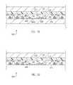
- FIG. 1is a cross-sectional view of a fan out build up substrate stackable package during fabrication in accordance with one embodiment
- FIGS. 2 , 3 , 4 , 5 , 6 , 7are cross-sectional views of the fan out build up substrate stackable package of FIG. 1 at later stages during fabrication in accordance with various embodiments;
- FIGS. 8 , 9 , 10are cross-sectional views of the fan out build up substrate stackable package of FIG. 7 at later stages during fabrication in accordance with various embodiments;
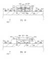
- FIG. 11is an enlarged cross-sectional view of the region XI of the fan out build up substrate stackable package of FIG. 10 in accordance with one embodiment
- FIG. 12is an enlarged cross-sectional view of the region XI of the fan out build up substrate stackable package of FIG. 10 in accordance with another embodiment
- FIG. 13is a cross-sectional view of a fan out build up substrate stackable package during fabrication in accordance with another embodiment
- FIGS. 14 , 15 , 16 , 17are cross-sectional views of the fan out build up substrate stackable package of FIG. 13 at later stages during fabrication in accordance with various embodiments;
- FIG. 18is a cross-sectional view of a fan out build up substrate stackable package during fabrication in accordance with yet another embodiment
- FIGS. 19 , 20 , 21 , 22 , 23 , 24are cross-sectional views of the fan out build up substrate stackable package of FIG. 18 at later stages during fabrication in accordance with various embodiments;
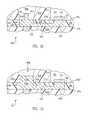
- FIG. 25is a cross-sectional view of a fan out build up substrate stackable package in accordance with another embodiment.
- FIG. 26is a cross-sectional view of a fan out build up substrate stackable package in accordance with one embodiment.
- FIG. 1is a cross-sectional view of a fan out build up substrate stackable package 100 during fabrication in accordance with one embodiment.
- an electronic component 102is mounted to a carrier 104 .
- electronic component 102is an integrated circuit chip, e.g., an active component.
- electronic component 102is a passive component such as a capacitor, resistor, or inductor.
- electronic component 102includes an active surface 106 and an opposite inactive surface 108 .
- Electronic component 102further includes bond pads 110 formed on active surface 106 and sides 112 extending between active surface 106 and inactive surface 108 .
- carrier 104includes an adhesive on an upper, e.g., first, surface 104 U of carrier 104 .
- Active surface 106 of electronic component 102is pressed into upper surface 104 U of carrier 104 and thus sticks to carrier 104 .
- an adhesiveis applied to active surface 106 of electronic component 102 , and this adhesive is pressed into carrier 104 to stick electronic component 102 to carrier 104 .
- FIG. 2is a cross-sectional view of fan out build up substrate stackable package 100 of FIG. 1 at a later stage during fabrication in accordance with one embodiment.
- electronic component 102is encapsulated in a dielectric package body 214 .
- package body 214is formed of mold compound.
- package body 214is formed of other dielectric materials such as hardened liquid encapsulant.
- Package body 214includes a lower, e.g., first, surface 214 L attached to upper surface 104 U of carrier 104 and an upper, e.g., second, surface 214 U.
- Package body 214completely encloses electronic component 102 including inactive surface 108 and sides 112 and the exposed portion of upper surface 104 U of carrier 104 .
- Package body 214is thicker having a thickness T1 greater than a thickness T2 of electronic component 102 . More particularly, upper surface 214 U is above and spaced apart from inactive surface 108 .
- FIG. 3is a cross-sectional view of fan out build up substrate stackable package 100 of FIG. 2 at a later stage during fabrication in accordance with one embodiment.
- package body 214is ground down from upper surface 214 U to expose inactive surface 108 of electronic component 102 .
- inactive surface 108is also ground down thus thinning both package body 214 and electronic component 102 .
- upper surface 214 U of package body 214 and inactive surface 108 of electronic component 102are parallel and coplanar.
- package body 214 and electronic component 102have an equal thickness T3 less than thicknesses T1, T2 prior to grinding. Thinning package body 214 and electronic component 102 minimizes the overall thickness of fan out build up substrate stackable package 100 . Generally, fan out build up substrate stackable package 100 is extremely thin resulting in extremely thin stacked assemblies. Grinding of package body 214 and electronic component 102 is optional, and in one embodiment, is not performed.
- package body 214is a relatively rigid material allowing carrier 104 ( FIG. 2 ) to be removed as illustrated in FIG. 3 .
- carrier 104is removed by peeling, etching, grinding, or other removal technique.
- a first buildup dielectric layer 316is applied to lower surface 214 L of package body 214 and active surface 106 of electronic component 102 including bond pads 110 . More particularly, an upper, e.g., first, surface 316 U is applied to lower surface 214 L of package body 214 and active surface 106 of electronic component 102 .
- First buildup dielectric layer 316further includes a lower, e.g., second, surface 316 L.
- a dielectric backside warpage control layer 318is applied to upper surface 214 U of package body 214 .
- backside warpage control layer 318is also applied to inactive surface 108 .
- Backside warpage control layer 318has a thermal coefficient of expansion similar or identical to first buildup dielectric layer 316 . More particularly, backside warpage control layer 318 expands and contracts at various temperatures in a similar manner to first buildup dielectric layer 316 . Accordingly, backside warpage control layer 318 offsets stress and associated warpage generated by thermal expansion and contraction of first buildup dielectric layer 316 . In this manner, backside warpage control layer 318 prevents warpage of fan out build up substrate stackable package 100 . However, formation of backside warpage control layer 318 is optional, and in one embodiment, backside warpage control layer 318 is not formed.
- FIG. 4is a cross-sectional view of fan out build up substrate stackable package 100 of FIG. 3 at a later stage during fabrication in accordance with one embodiment.
- a circuit pattern artifact 420is formed in first buildup dielectric layer 316 .
- Circuit pattern artifact 420is formed using laser ablation, selective etching, or other technique.
- Circuit pattern artifact 420is a positive image of the circuit pattern to be formed in first buildup dielectric layer 316 .
- Circuit pattern artifact 420includes bond pad via apertures 422 extending entirely through first buildup dielectric layer 316 and exposing bond pads 110 .
- Circuit pattern artifact 420further includes trace channels 424 and via capture pad openings 426 .
- FIG. 5is a cross-sectional view of fan out build up substrate stackable package 100 of FIG. 4 at a later stage during fabrication in accordance with one embodiment.
- a circuit pattern 528is formed within circuit pattern artifact 420 .
- circuit pattern 528sometimes called a first metal layer, is formed by plating an electrically conductive material such as copper within circuit pattern artifact 420 .
- circuit pattern 528is formed within first buildup dielectric layer 316 .
- circuit pattern 528includes one or more metal layers. For example, initially a solder wettable layer such as gold is plated in circuit pattern artifact 420 to partially fill circuit pattern artifact 420 . Circuit pattern artifact 420 is then completely filled with a second metal such as copper. In this manner, the exposed surfaces of via capture pads of circuit pattern 528 are solder wettable as discussed in greater detail below.
- a solder wettable layersuch as gold is plated in circuit pattern artifact 420 to partially fill circuit pattern artifact 420 .
- Circuit pattern artifact 420is then completely filled with a second metal such as copper. In this manner, the exposed surfaces of via capture pads of circuit pattern 528 are solder wettable as discussed in greater detail below.
- Circuit pattern 528includes electrically conductive bond pad vias 530 formed in bond pad via apertures 422 and electrically connected to bond pads 110 .
- Circuit pattern 528further includes electrically conductive traces 532 formed within trace channels 424 and electrically conductive via capture pads 534 formed within via capture pad openings 426 .
- circuit pattern 528is set forth as containing particular features, e.g., bond pad vias 530 , traces 532 , and via capture pads 534 , in light of this disclosure, those of skill in the art will understand that a circuit pattern can be formed with other and/or different features depending on the particular signal routing desired.
- traces 532are formed on lower surface 316 L of first buildup dielectric layer 316 .
- FIG. 6is a cross-sectional view of fan out build up substrate stackable package 100 of FIG. 5 at a later stage during fabrication in accordance with one embodiment.
- an upper, e.g., first, surface 636 U of a second buildup dielectric layer 636is applied to lower surface 316 L of first buildup dielectric layer 316 and to circuit pattern 528 .
- a circuit pattern artifact 638is formed in a lower, e.g., second, surface 636 L of second buildup dielectric layer 636 .
- Circuit pattern artifact 638is formed using laser ablation, selective etching, or other technique.
- Circuit pattern artifact 638is a positive image of the circuit pattern to be formed in second buildup dielectric layer 636 .
- Circuit pattern artifact 638includes blind via apertures 640 extending entirely through second buildup dielectric layer 636 and exposing circuit pattern 528 .
- Circuit pattern artifact 638further includes trace channels 642 and land openings 644 .
- FIG. 7is a cross-sectional view of fan out build up substrate stackable package 100 of FIG. 6 at a later stage during fabrication in accordance with one embodiment.
- a circuit pattern 746is formed within circuit pattern artifact 638 .
- circuit pattern 746is formed by plating an electrically conductive material such as copper within circuit pattern artifact 638 .
- circuit pattern 746includes one or more metal layers.
- circuit pattern 746sometimes called a second circuit pattern, is formed within second buildup dielectric layer 636 .
- Circuit pattern 746includes electrically conductive circuit pattern vias 748 formed in blind via apertures 640 and electrically connected to circuit pattern 528 .
- Circuit pattern 746further includes electrically conductive traces 750 formed in trace channels 642 and electrically conductive lands 752 formed in land openings 644 .
- circuit pattern 746is set forth as containing particular features, e.g., circuit pattern vias 748 , traces 750 , and lands 752 , in light of this disclosure, those of skill in the art will understand that a circuit pattern can be formed with other and/or different features depending on the particular signal routing desired.
- traces 750 and lands 752are formed on lower surface 636 L of second buildup dielectric layer 636 .
- FIG. 8is a cross-sectional view of fan out build up substrate stackable package 100 of FIG. 7 at a later stage during fabrication in accordance with one embodiment.
- a dielectric solder mask 854is applied to lower surface 636 L of second buildup dielectric layer 636 and patterned to expose lands 752 of circuit pattern 746 .
- Interconnection balls 856e.g., solder, are formed on lands 752 .
- Interconnection balls 856are distributed in a ball grid array (BGA) in one embodiment.
- Interconnection balls 856are reflowed, i.e., heated to a melt and re-solidified, to mount fan out build up substrate stackable package 100 to another structure such as a printed circuit motherboard.
- the formation of interconnection balls 856is optional, and in one embodiment, interconnection balls 856 are not formed.
- via capture pad apertures 858are formed, e.g., using laser ablation, through package body 214 and backside warpage control layer 318 if backside warpage control layer 318 is formed. Via capture pad apertures 858 extend through package body 214 from upper surface 214 U to lower surface 214 L and expose via capture pads 534 of circuit pattern 528 .
- the exposed surfaces of via capture pads 534 exposed through via capture pad apertures 858include a solder wettable layer.
- a solder wettable layere.g., nickel, gold, organic solderability protectant (OSP) is formed on via capture pads 534 through via capture pad apertures 858 .
- OSPorganic solderability protectant
- via capture pad apertures 858expose via capture pads 534 of circuit pattern 528 .
- Thisfacilitates direct connection to circuit pattern 528 , i.e., the first metal layer, of fan out build up substrate stackable package 100 .
- additional stacked structuressuch as integrated circuit dies, other active components, passive components, and/or stacked electronic component packages, are mounted to (stacked) on fan out build up substrate stackable package 100 by placing solder balls of the additional structures within via capture pad apertures 858 . The solder balls of the stacked structures are reflowed thus physically and electrically connecting the solder balls and thus the stacked structures to via capture pads 534 of circuit pattern 528 .
- backside warpage control layer 318remains and covers the entire upper surface 214 U of package body 214 .
- the thickness of backside warpage control layer 318is approximately equal to the typical gap between upper surface 214 U of package body 214 and the lower surface of the stacked structure stacked upon fan out build up substrate stackable package 100 .
- backside warpage control layer 318includes a B-stage epoxy. This B-stage epoxy is cured during reflow mounting of the stacked structure thus bonding the stacked structure to upper surface 214 U and inactive surface 108 of electronic component 102 .
- FIG. 9is a cross-sectional view of fan out build up substrate stackable package 100 of FIG. 7 at a later stage during fabrication in accordance with another embodiment.
- solder mask 854optional interconnection balls 856 , and via capture pad apertures 858 are formed as discussed above in reference to FIG. 8 .
- backside warpage control layer 318is removed from the outer periphery of upper surface 214 U of package body 214 . More particularly, backside warpage control layer 318 remains only on and covers the central region of upper surface 214 U of package body 214 inwards of via capture pad apertures 858 .
- FIG. 10is a cross-sectional view of fan out build up substrate stackable package 100 of FIG. 7 at a later stage during fabrication in accordance with yet another embodiment.
- solder mask 854is formed as discussed above in reference to FIG. 8 .
- backside warpage control layer 318is completely removed as illustrated in FIG. 10 .
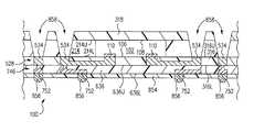
- FIG. 11is an enlarged cross-sectional view of the region XI of fan out build up substrate stackable package 100 of FIG. 10 in accordance with one embodiment.
- circuit pattern 528includes bond pad via 530 , trace 532 , and via capture pad 534 .
- Bond pad via 530is electrically connected to via capture pad 534 by trace 532 .
- via capture pad 534extends entirely through first buildup dielectric layer 316 but does not extend into package body 214 . Accordingly, an upper, first, surface 534 U of via capture pad 534 is parallel to and coplanar with lower surface 214 L of package body 214 and active surface 106 of electronic component 102 . Active surface 106 of electronic component 102 and lower surface 214 L of package body 214 are also parallel to and coplanar with one another.
- via capture pad pin apertures 1160are formed in package body 214 (via capture pad pin apertures 1160 are not illustrated in the embodiment of FIG. 4 , see FIG. 11 for example).
- via capture pad pin apertures 1160are cylindrical openings formed by laser ablating into package body 214 through via capture pad openings 426 .
- Via capture pad pin apertures 1160extend from respective via capture pad openings 426 and into package body 214 .
- via capture pad pin apertures 1160are filled with the electrically conductive material of circuit pattern 528 to form via capture pad pins 1162 (via capture pad pins 1162 are not illustrated in the embodiment of FIG. 5 , see FIG. 11 for example).
- Via capture pad pins 1162protrude upwards from upper surfaces 534 U of via capture pads 534 and into package body 214 prior to formation of via capture pad apertures 858 .
- Via capture pad pins 1162have a smaller diameter than via capture pads 534 .
- via capture pad pins 1162protrude upwards from upper surfaces 534 U of via capture pads 534 and into via capture pad apertures 858 .
- via capture pad pins 1162provide controlled collapse of the stacked structure solder balls, e.g., BGA balls. In this manner, via capture pad pins 1162 minimized the possibility of open solder joints, i.e., a failed solder connection, between the stacked structure and via capture pads 534 .
- FIG. 12is an enlarged cross-sectional view of the region XI of fan out build up substrate stackable package 100 of FIG. 10 in accordance with another embodiment.
- circuit pattern 528includes bond pad via 530 , trace 532 , and via capture pad 534 .
- Bond pad via 530is electrically connected to via capture pad 534 by trace 532 .
- via capture pad 534extends entirely through first buildup dielectric layer 316 and extends into package body 214 . Accordingly, upper surface 534 U of via capture pad 534 is parallel to but elevated above lower surface 214 L of package body 214 and active surface 106 of electronic component 102 . More particularly, upper surface 534 U of via capture pad 534 is between lower surface 214 L and upper surface 214 U of package body 214 . Via capture pad 534 is embedded into package body 214 .
- via capture pad openings 426are formed entirely through first buildup dielectric layer 316 and into package body 214 (via capture pad openings 426 do not extend into package body 214 in the embodiment illustrated in FIG. 4 , see FIG. 12 for example). In one embodiment, via capture pad openings 426 are formed by laser ablating into package body 214 .
- Via capture pads 534protrude upwards and extend into package body 214 (via capture pads 534 do not protrude into package body 214 in the embodiment illustrated in FIG. 5 , see FIG. 12 for example).
- increased thickness via capture pads 534reduce the distance into which the solder balls of the stacked structure must extend into via capture pad apertures 858 to contact capture pads 534 . In this manner, increased thickness via capture pads 534 minimized the possibility of open solder joints, i.e., a failed solder connection, between the stacked structure and via capture pads 534 . Further, increased thickness via capture pads 534 adjust the seating plane of the stacked structure to optimize the gap between fan out build up substrate stackable package 100 and the stacked structure.
- fan out build up substrate stackable package 100includes first buildup dielectric layer 316 and second buildup dielectric layer 636 , i.e., two buildup dielectric layers.
- first buildup dielectric layer 316 and second buildup dielectric layer 636i.e., two buildup dielectric layers.
- a fan out build up substrate stackable package 1300is fabricated using only a single buildup dielectric layer and thus minimizing the overall thickness of fan out build up substrate stackable package 1300 .
- FIG. 13is a cross-sectional view of a fan out build up substrate stackable package 1300 during fabrication in accordance with another embodiment.
- an upper, e.g., first, surface 1302 U of a dielectric film 1302is applied to active surface 106 including bond pads 110 of electronic component 102 .
- a sheet of dielectric film 1302is applied to a wafer comprising a plurality of electronic components 102 prior to dicing (cutting) of the wafer to form singulated electronic components 102 .
- This sheet of dielectric film 1302is applied after formation of the Under Bump Metallization (UBM) and prior to wafer dicing.
- UBMUnder Bump Metallization
- the wafer including sheet of dielectric film 1302is diced to form singulated electronic components 102 each having a dielectric film 1302 attached.
- a lower, e.g., second, surface 1302 L of dielectric film 1302is mounted to upper surface 104 U of carrier 104 .
- Dielectric film 1302further includes sides 1304 extending between upper surface 1302 U and lower surface 1302 L of dielectric film 1302 . Sides 1304 are coplanar with sides 112 of electronic component 102 .
- FIG. 14is a cross-sectional view of fan out build up substrate stackable package 1300 of FIG. 13 at a later stage during fabrication in accordance with one embodiment.
- electronic component 102 and dielectric film 1302are encapsulated in package body 214 .
- electronic component 102 , dielectric film 1302 , and carrier 104are placed into a mold and mold compound is injected into the mold and around electronic component 102 and dielectric film 1302 .
- This mold compoundhardens to form package body 214 .
- Package body 214completely encloses electronic component 102 , dielectric film 1302 , and the exposed portion of upper surface 104 U of carrier 104 . More particularly, package body 214 completely encloses inactive surface 108 and sides 112 of electronic component 102 . Further, package body 214 completely encloses sides 1304 of dielectric film 1302 .
- Package body 214is thicker having a thickness T1 greater than a thickness T4 of electronic component 102 and dielectric film 1302 . More particularly, upper surface 214 U is above and spaced apart from inactive surface 108 .
- FIG. 15is a cross-sectional view of fan out build up substrate stackable package 1300 of FIG. 14 at a later stage during fabrication in accordance with one embodiment.
- package body 214is ground down from upper surface 214 U to expose inactive surface 108 of electronic component 102 .
- inactive surface 108is also ground down thus thinning both package body 214 and electronic component 102 .
- package body 214 and electronic component 102have an equal thickness T5 less than thicknesses T1, T4 prior to grinding. Thinning package body 214 and electronic component 102 minimizes the overall thickness of fan out build up substrate stackable package 1300 . Grinding of package body 214 and electronic component 102 is optional, and in one embodiment, is not performed.
- Package body 214is a relatively rigid material allowing carrier 104 ( FIG. 14 ) to be removed as illustrated in FIG. 15 .
- carrier 104is removed by peeling, etching, grinding, or other removal technique.
- a backside warpage control layer 318is applied to upper surface 214 U of package body 214 .
- backside warpage control layer 318is also applied to inactive surface 108 .
- FIG. 16is a cross-sectional view of fan out build up substrate stackable package 1300 of FIG. 15 at a later stage during fabrication in accordance with one embodiment.
- a circuit pattern artifact 1620is formed in dielectric film 1302 and package body 214 .
- Circuit pattern artifact 1620is formed using laser ablation in one embodiment.
- Circuit pattern artifact 1620is similar or identical to circuit pattern artifact 420 of FIG. 4 except that circuit pattern artifact 1620 is formed within dielectric film 1302 and package body 214 whereas circuit pattern artifact 420 of FIG. 4 is formed in first buildup dielectric layer 316 .
- Circuit pattern artifact 1620is a positive image of the circuit pattern to be formed in dielectric film 1302 and package body 214 .
- Circuit pattern artifact 1620includes bond pad via apertures 1622 extending entirely through dielectric film 1302 and exposing bond pads 110 .
- Circuit pattern artifact 420further includes trace channels 1624 and via capture pad openings 1626 .
- Trace channels 1624are formed within both dielectric film 1302 and package body 214 . Trace channels 1624 extend between bond pad via apertures 1622 and via capture pad openings 1626 .
- FIG. 17is a cross-sectional view of fan out build up substrate stackable package 1300 of FIG. 16 at a later stage during fabrication in accordance with one embodiment.
- a circuit pattern 1728is formed within circuit pattern artifact 1620 .
- circuit pattern 1728sometimes called a first metal layer, is formed by plating an electrically conductive material such as copper within circuit pattern artifact 1620 .
- Circuit pattern 1728is similar or identical to circuit pattern 528 of FIG. 5 except that circuit pattern 1728 is formed within dielectric film 1302 and package body 214 whereas circuit pattern 528 of FIG. 5 is formed in first buildup dielectric layer 316 .
- circuit pattern 1728includes one or more metal layers. For example, initially a solder wettable layer such as nickel and/or gold is plated in circuit pattern artifact 1620 to partially fill circuit pattern artifact 1620 . Circuit pattern artifact 1620 is then completely filled with a second metal such as copper. In this manner, the exposed surfaces of via capture pads of circuit pattern 1728 are solder wettable as discussed in greater detail below.
- a solder wettable layersuch as nickel and/or gold is plated in circuit pattern artifact 1620 to partially fill circuit pattern artifact 1620 .
- Circuit pattern artifact 1620is then completely filled with a second metal such as copper. In this manner, the exposed surfaces of via capture pads of circuit pattern 1728 are solder wettable as discussed in greater detail below.
- Circuit pattern 1728includes electrically conductive bond pad vias 1730 formed in bond pad via apertures 1622 and electrically connected to bond pads 110 .
- Bond pad vias 1730are formed within dielectric film 1302 .
- Circuit pattern 1728further includes electrically conductive traces 1732 formed within trace channels 1624 and electrically conductive via capture pads 1734 formed within via capture pad openings 1626 .
- Traces 1732are formed within both dielectric film 1302 and package body 214 .
- Via capture pads 1734are formed within package body 214 .
- circuit pattern 1728is set forth as containing particular features, e.g., bond pad vias 1730 , traces 1732 , and via capture pads 1734 , in light of this disclosure, those of skill in the art will understand that a circuit pattern can be formed with other and/or different features depending on the particular signal routing desired. Further, instead of being embedded inside of dielectric film 1302 and package body 214 , in another embodiment, traces 1732 are formed on lower surfaces 1302 L, 214 L of dielectric film 1302 and package body 214 , respectively.
- an upper, e.g., first, surface 636 U of a buildup dielectric layer 636is applied to lower surfaces 214 L, 1302 L of package body 214 and dielectric film 1302 , respectively, and to circuit pattern 1728 .
- a circuit pattern artifact 638is formed in a lower, e.g., second, surface 636 L of buildup dielectric layer 636 .
- Circuit pattern artifact 638is formed using laser ablation, selective etching, or other technique.
- Buildup dielectric layer 636 and circuit pattern artifact 638 of FIG. 17are similar or identical to second buildup dielectric layer 636 and circuit pattern artifact 638 as described above in reference to FIG. 6 .
- buildup dielectric layer 636is applied directly to lower surfaces 214 L, 1302 L of package body 214 and dielectric film 1302 , respectively, and to circuit pattern 1728 thus avoiding application of first buildup dielectric layer 316 as also illustrated in FIG. 6 .
- Circuit pattern artifact 638is a positive image of the circuit pattern to be formed in buildup dielectric layer 636 .
- Circuit pattern artifact 638includes blind via apertures 640 extending entirely through buildup dielectric layer 636 and exposing circuit pattern 1728 .
- Circuit pattern artifact 638further includes trace channels 642 and land openings 644 .
- Fan out build up substrate stackable package 1300 of FIG. 17is further processed as set forth above in reference to the embodiment of FIGS. 7 , 8 , 9 , 10 , 11 , 12 and so these fabrication operations are not repeated.
- a notable exceptionis that via capture pad apertures 858 of FIG. 8 extend to and expose via capture pads 1734 of circuit pattern 1728 of FIG. 17 instead of via capture pads 534 of FIG. 8 .
- FIG. 18is a cross-sectional view of a fan out build up substrate stackable package 1800 during fabrication in accordance with yet another embodiment.
- via capture pads 1802are formed on an upper, e.g., first, surface 1804 U of a carrier 1804 .
- carrier 1804is an electrically conductive material such as copper. Via capture pads 1802 are plated on carrier 1804 using carrier 1804 as a plating electrode.
- via capture pads 1802include an etch stop layer 1808 and a solder wettable layer 1810 .
- Carrier 1804e.g., copper
- Solder wettable layer 1810e.g., gold
- solder 1812is applied to via capture pads 1802 .
- Application of solder 1812is optional, and in one embodiment, solder 1812 is not applied.
- active surface 106 of electronic component 102is mounted to upper surface 1804 U of carrier 1804 by an adhesive 1806 , e.g., a die attach material.
- adhesive 1806is a strong adhesive thus avoiding undesirable movement of electronic component 102 on carrier 1804 during molding.
- FIG. 19is a cross-sectional view of fan out build up substrate stackable package 1800 of FIG. 18 at a later stage during fabrication in accordance with one embodiment.
- electronic component 102 , via capture pads 1802 , and solder 1812are encapsulated in a dielectric package body 214 .
- electronic component 102via capture pads 1802 , solder 1812 and carrier 1804 are placed into a mold and mold compound is injected into the mold and around electronic component 102 , via capture pads 1802 , and solder 1812 to form package body 214 .
- Package body 214includes a lower, e.g., first, surface 214 L attached to upper surface 1804 U of carrier 1804 and an upper, e.g., second, surface 214 U.
- Package body 214completely encloses electronic component 102 including inactive surface 108 and sides 112 and the exposed portion of upper surface 1804 U of carrier 1804 . Further, package body 214 completely encloses via capture pads 1802 and solder 1812 .
- Package body 214is thicker having a thickness T1 greater than a thickness T2 of electronic component 102 including adhesive 1806 .
- the thickness of adhesive 1806is generally negligible so electronic component 102 shall be referred to as having thickness T2. More particularly, upper surface 214 U is above and spaced apart from inactive surface 108 .
- FIG. 20is a cross-sectional view of fan out build up substrate stackable package 1800 of FIG. 19 at a later stage during fabrication in accordance with one embodiment.
- package body 214is ground down from upper surface 214 U to expose inactive surface 108 of electronic component 102 .
- inactive surface 108is also ground down thus thinning both package body 214 and electronic component 102 .
- package body 214 and electronic component 102have an equal thickness T3 less than thicknesses T1, T2 prior to grinding. Thinning package body 214 and electronic component 102 minimizes the overall thickness of fan out build up substrate stackable package 1800 . Grinding of package body 214 and electronic component 102 is optional, and in one embodiment, is not performed.
- FIG. 21is a cross-sectional view of fan out build up substrate stackable package 1800 of FIG. 20 at a later stage during fabrication in accordance with one embodiment.
- a backside warpage control layer 318is applied to upper surface 214 U of package body 214 .
- backside warpage control layer 318is also applied to inactive surface 108 .
- backside warpage control layer 318is applied to a carrier 2114 , e.g., stainless steel.
- Carrier 2114adds rigidity and support to fan out build up substrate stackable package 1800 during fabrication as set forth below.
- Application of backside warpage control layer 318 and/or carrier 2114is optional, and in one embodiment, only backside warpage control layer 318 is applied. In another embodiment, neither backside warpage control layer 318 nor carrier 2114 are applied.
- FIG. 22is a cross-sectional view of fan out build up substrate stackable package 1800 of FIG. 21 at a later stage during fabrication in accordance with one embodiment.
- carrier 1804is removed.
- carrier 1804is copper and is removed by etching.
- etch stop layer 1808is selectively etchable compared to carrier 1804 and thus provides an etch stop.
- backside warpage control layer 318 and adhesive 1806protect electronic component 102 during the etching process.
- carrier 1804is stainless steel and is removed by peeling.
- FIG. 23is a cross-sectional view of fan out build up substrate stackable package 1800 of FIG. 22 at a later stage during fabrication in accordance with one embodiment.
- a first buildup dielectric layer 316is applied to lower surface 214 L of package body 214 , via capture pads 1802 , and adhesive 1806 .
- a circuit pattern artifact 420is formed in first buildup dielectric layer 316 .
- Circuit pattern artifact 420is formed using laser ablation, selective etching, or other technique.
- Circuit pattern artifact 420is a positive image of the circuit pattern to be formed in first buildup dielectric layer 316 .
- Circuit pattern artifact 420includes bond pad via apertures 422 extending entirely through first buildup dielectric layer 316 , adhesive 1806 and exposing bond pads 110 .
- Circuit pattern artifact 420further includes trace channels 424 and capture pad via apertures 2316 .
- capture pad via apertures 2316are openings extending through first buildup dielectric layer 316 and exposing via capture pads 1802 .
- circuit pattern 528is formed within circuit pattern artifact 420 .
- circuit pattern 528is formed by plating an electrically conductive material such as copper within circuit pattern artifact 420 .
- Circuit pattern 528includes electrically conductive bond pad vias 530 formed in bond pad via apertures 422 and electrically connected to bond pads 110 .
- Circuit pattern 528further includes electrically conductive traces 532 formed within trace channels 424 and electrically conductive capture pad vias 2318 formed within capture pad via apertures 2316 .
- Capture pad vias 2318extend through first buildup dielectric layer 316 and are electrically connected to via capture pads 1802 .
- circuit pattern 528is set forth as containing particular features, e.g., bond pad vias 530 , traces 532 , and capture pad vias 2318 , in light of this disclosure, those of skill in the art will understand that a circuit pattern can be formed with other and/or different features depending on the particular signal routing desired.
- a second buildup dielectric layer 636is applied to first buildup dielectric layer 316 and to circuit pattern 528 .
- a circuit pattern artifact 638is formed in second buildup dielectric layer 636 .
- Circuit pattern artifact 638is formed using laser ablation, selective etching, or other technique.
- Circuit pattern artifact 638is a positive image of the circuit pattern to be formed in second buildup dielectric layer 636 .
- Circuit pattern artifact 638includes blind via apertures 640 extending entirely through second buildup dielectric layer 636 and exposing circuit pattern 528 .
- Circuit pattern artifact 638further includes trace channels 642 and land openings 644 .
- circuit pattern 746is formed within circuit pattern artifact 638 .
- circuit pattern 746is formed by plating an electrically conductive material such as copper within circuit pattern artifact 638 .
- circuit pattern 746includes one or more metal layers.
- Circuit pattern 746includes electrically conductive circuit pattern vias 748 formed in blind via apertures 640 and electrically connected to circuit pattern 528 .
- Circuit pattern 746further includes electrically conductive traces 750 formed in trace channels 642 and electrically conductive lands 752 formed in land openings 644 .
- circuit pattern 746is set forth as containing particular features, e.g., circuit pattern vias 748 , traces 750 , and lands 752 , in light of this disclosure, those of skill in the art will understand that a circuit pattern can be formed with other and/or different features depending on the particular signal routing desired.
- a dielectric solder mask 854is applied to second buildup dielectric layer 636 and patterned to expose lands 752 of circuit pattern 746 .
- Interconnection balls 856e.g., solder, are formed on lands 752 . Interconnection balls 856 are distributed in a ball grid array (BGA) in one embodiment. The formation of interconnection balls 856 is optional, and in one embodiment, interconnection balls 856 are not formed.
- BGAball grid array
- FIG. 24is a cross-sectional view of fan out build up substrate stackable package 1800 of FIG. 23 at a later stage during fabrication in accordance with one embodiment.
- carrier 2114FIG. 23
- backside warpage control layer 318exposed as illustrated in FIG. 24 .
- via capture pad apertures 2420are formed, e.g., using laser ablation, through package body 214 and backside warpage control layer 318 if backside warpage control layer 318 is formed. Via capture pad apertures 2420 expose via capture pads 1802 or solder 1812 if solder 1812 is formed. Generally, via capture pad apertures 2420 are aligned with respective via capture pads 1802 .
- FIG. 25is a cross-sectional view of a fan out build up substrate stackable package 2500 in accordance with another embodiment.
- Fan out build up substrate stackable package 2500 of FIG. 25is similar to fan out build up substrate stackable package 1800 of FIG. 18 and only the significant differences are discussed below.
- electrically conductive through vias 2502are formed through electronic component 102 .
- through vias 2502extend between active surface 106 and inactive surface 108 .
- the ends of through vias 2502 at active surface 106define active surface through via terminals 2504 .
- the ends of through vias 2502 at inactive surface 108define inactive surface through via terminals 2506 .
- Active surface through via terminals 2504are electrically connected to inactive surface through via terminals 2506 by through vias 2502 .
- a stacked flip chip electronic component 2508e.g., an active components such as an integrated circuit die, a passive component, and/or electronic component package, is mounted to electronic component 102 .
- stacked flip chip electronic component 2508includes an active surface 2510 having bond pads 2512 thereon. Stacked flip chip electronic component 2508 further includes an inactive surface 2514 and sides 2516 extending between active surface 2510 and inactive surface 2514 .
- Bond pads 2512are physically and electrically mounted to inactive surface through via terminals 2506 by flip chip bumps 2518 , e.g., solder.
- flip chip bumps 2518e.g., solder.
- an underfill 2520is applied between active surface 2510 of stacked flip chip electronic component 2508 and inactive surface 108 of electronic component 102 and around flip chip bumps 2518 .
- Fan out build up substrate stackable package 2500 of FIG. 25is further process as set forth above in reference to the embodiment of FIGS. 19 , 20 , 21 , 22 , 23 , 24 and so these fabrication operations are not repeated.
- both stacked flip chip electronic component 2508 and electronic component 102are encapsulated within package body 214 .
- only electronic component 102is encapsulated within package body 214 .
- package body 214is not ground down or, if ground down, is ground down to expose inactive surface 2514 of stacked flip chip electronic component 2508 . In contrast, recall that in FIG. 20 , package body 214 is ground down to expose inactive surface 108 of electronic component 102 .
- bond pad vias 530 of circuit pattern 528extend entirely through first buildup dielectric layer 316 , adhesive 1806 and are electrically connected to both bond pads 110 and active surface through via terminals 2504 . In contrast, recall that in FIG. 23 , bond pad vias 530 are electrically connected to only bond pads 110 .
- FIG. 26is a cross-sectional view of a fan out build up substrate stackable package 2600 in accordance with one embodiment.
- Fan out build up substrate stackable package 2600 of FIG. 26is similar to fan out build up substrate stackable package 1800 of FIG. 18 and only the significant differences are discussed below.
- a stacked wirebond electronic component 2602e.g., an active components such as integrated circuit die, a passive component, and/or electronic component package, is mounted to electronic component 102 .
- stacked wirebond electronic component 2602includes an active surface 2604 having bond pads 2606 thereon.
- Stacked wirebond electronic component 2602further includes an inactive surface 2608 and sides 2610 extending between active surface 2604 and inactive surface 2608 .
- Inactive surface 2608 of stacked wirebond electronic component 2602is mounted to inactive surface 108 of electronic component 102 with an adhesive 2612 .
- Bond pads 2606 of stacked wirebond electronic component 2602are electrically connected to via capture pads 1802 with bond wires 2614 .
- the via capture pads 1802 electrically connected to bond wires 2614are formed without solder 1812 as illustrated in FIG. 26 .
- Fan out build up substrate stackable package 2600 of FIG. 26is further process as set forth above in reference to the embodiment of FIGS. 19 , 20 , 21 , 22 , 23 , 24 and so these fabrication operations are not repeated.
- both stacked wirebond electronic component 2602 , electronic component 102 , and bond wires 2614are encapsulated within package body 214 .
- only electronic component 102is encapsulated within package body 214 .
- package body 214is not ground down or, if ground down, is only ground down such that a sufficient amount of package body 214 remains to enclose bond wires 2614 . In contrast, recall that in FIG. 20 , package body 214 is ground down to expose inactive surface 108 of electronic component 102 .
- a plurality of packagesare formed simultaneously in an array using the methods as described above.
- the arrayis singulated to singulate the individual packages from one another.
Landscapes
- Engineering & Computer Science (AREA)
- Microelectronics & Electronic Packaging (AREA)
- Computer Hardware Design (AREA)
- Power Engineering (AREA)
- Physics & Mathematics (AREA)
- Condensed Matter Physics & Semiconductors (AREA)
- General Physics & Mathematics (AREA)
- Manufacturing & Machinery (AREA)
- Production Of Multi-Layered Print Wiring Board (AREA)
Abstract
Description
Claims (17)
Priority Applications (1)
| Application Number | Priority Date | Filing Date | Title |
|---|---|---|---|
| US12/573,466US8796561B1 (en) | 2009-10-05 | 2009-10-05 | Fan out build up substrate stackable package and method |
Applications Claiming Priority (1)
| Application Number | Priority Date | Filing Date | Title |
|---|---|---|---|
| US12/573,466US8796561B1 (en) | 2009-10-05 | 2009-10-05 | Fan out build up substrate stackable package and method |
Publications (1)
| Publication Number | Publication Date |
|---|---|
| US8796561B1true US8796561B1 (en) | 2014-08-05 |
Family
ID=51229028
Family Applications (1)
| Application Number | Title | Priority Date | Filing Date |
|---|---|---|---|
| US12/573,466Active2031-05-29US8796561B1 (en) | 2009-10-05 | 2009-10-05 | Fan out build up substrate stackable package and method |
Country Status (1)
| Country | Link |
|---|---|
| US (1) | US8796561B1 (en) |
Cited By (25)
| Publication number | Priority date | Publication date | Assignee | Title |
|---|---|---|---|---|
| US20130154105A1 (en)* | 2011-12-14 | 2013-06-20 | Byung Tai Do | Integrated circuit packaging system with routable trace and method of manufacture thereof |
| US20140103527A1 (en)* | 2012-03-23 | 2014-04-17 | Stats Chippac, Ltd. | Semiconductor Device and Method of Forming a POP Device with Embedded Vertical Interconnect Units |
| US20140154842A1 (en)* | 2012-01-20 | 2014-06-05 | Siliconware Precision Industries Co., Ltd. | Carrier, semiconductor package and fabrication method thereof |
| US20150008566A1 (en)* | 2013-07-02 | 2015-01-08 | Texas Instruments Incorporated | Method and structure of panelized packaging of semiconductor devices |
| US9093457B2 (en) | 2012-08-22 | 2015-07-28 | Freescale Semiconductor Inc. | Stacked microelectronic packages having patterned sidewall conductors and methods for the fabrication thereof |
| US9190390B2 (en) | 2012-08-22 | 2015-11-17 | Freescale Semiconductor Inc. | Stacked microelectronic packages having sidewall conductors and methods for the fabrication thereof |
| US9263420B2 (en)* | 2013-12-05 | 2016-02-16 | Freescale Semiconductor, Inc. | Devices and stacked microelectronic packages with package surface conductors and methods of their fabrication |
| US9299670B2 (en) | 2013-03-14 | 2016-03-29 | Freescale Semiconductor, Inc. | Stacked microelectronic packages having sidewall conductors and methods for the fabrication thereof |
| US9305911B2 (en) | 2013-12-05 | 2016-04-05 | Freescale Semiconductor, Inc. | Devices and stacked microelectronic packages with package surface conductors and adjacent trenches and methods of their fabrication |
| US20160219710A1 (en)* | 2015-01-22 | 2016-07-28 | Samsung Electro-Mechanics Co., Ltd. | Electronic component embedded printed circuit board and method of manufacturing the same |
| US20160276239A1 (en)* | 2011-09-23 | 2016-09-22 | STATS ChipPAC Pte. Ltd. | Semiconductor Device and Method of Forming Stacked Vias Within Interconnect Structure for FO-WLCSP |
| US9524950B2 (en) | 2013-05-31 | 2016-12-20 | Freescale Semiconductor, Inc. | Stacked microelectronic packages having sidewall conductors and methods for the fabrication thereof |
| US9831219B2 (en)* | 2016-04-20 | 2017-11-28 | Powertech Technology Inc. | Manufacturing method of package structure |
| US9837303B2 (en) | 2012-03-23 | 2017-12-05 | STATS ChipPAC Pte. Ltd. | Semiconductor method and device of forming a fan-out device with PWB vertical interconnect units |
| US9865525B2 (en) | 2012-03-23 | 2018-01-09 | STATS ChipPAC Pte. Ltd. | Semiconductor method and device of forming a fan-out PoP device with PWB vertical interconnect units |
| US9929072B2 (en) | 2013-07-02 | 2018-03-27 | Texas Instruments Incorporated | Packaged semiconductor devices |
| US10049964B2 (en) | 2012-03-23 | 2018-08-14 | STATS ChipPAC Pte. Ltd. | Semiconductor device and method of forming a fan-out PoP device with PWB vertical interconnect units |
| US10177077B2 (en) | 2017-04-13 | 2019-01-08 | Powertech Technology Inc. | Chip structure having redistribution layer |
| KR20190003331A (en)* | 2017-06-30 | 2019-01-09 | 타이완 세미콘덕터 매뉴팩쳐링 컴퍼니 리미티드 | Semiconductor device with shielding structure for cross-talk reduction |
| US10388607B2 (en) | 2014-12-17 | 2019-08-20 | Nxp Usa, Inc. | Microelectronic devices with multi-layer package surface conductors and methods of their fabrication |
| US10504857B2 (en)* | 2013-07-31 | 2019-12-10 | Amkor Technology, Inc. | Semiconductor package structure for improving die warpage and manufacturing method thereof |
| US10546833B2 (en) | 2009-12-07 | 2020-01-28 | Amkor Technology, Inc. | Method of forming a plurality of electronic component packages |
| CN111816636A (en)* | 2019-04-10 | 2020-10-23 | 欣兴电子股份有限公司 | Package carrier board and package structure |
| US10879144B2 (en) | 2018-08-14 | 2020-12-29 | Texas Instruments Incorporated | Semiconductor package with multilayer mold |
| US11302649B2 (en) | 2017-06-30 | 2022-04-12 | Taiwan Semiconductor Manufacturing Company, Ltd. | Semiconductor device with shielding structure for cross-talk reduction |
Citations (514)
| Publication number | Priority date | Publication date | Assignee | Title |
|---|---|---|---|---|
| US2596993A (en) | 1949-01-13 | 1952-05-20 | United Shoe Machinery Corp | Method and mold for covering of eyelets by plastic injection |
| US3435815A (en) | 1966-07-15 | 1969-04-01 | Micro Tech Mfg Inc | Wafer dicer |
| US3734660A (en) | 1970-01-09 | 1973-05-22 | Tuthill Pump Co | Apparatus for fabricating a bearing device |
| US3838984A (en) | 1973-04-16 | 1974-10-01 | Sperry Rand Corp | Flexible carrier and interconnect for uncased ic chips |
| US3868724A (en) | 1973-11-21 | 1975-02-25 | Fairchild Camera Instr Co | Multi-layer connecting structures for packaging semiconductor devices mounted on a flexible carrier |
| US3916434A (en) | 1972-11-30 | 1975-10-28 | Power Hybrids Inc | Hermetically sealed encapsulation of semiconductor devices |
| US4054238A (en) | 1976-03-23 | 1977-10-18 | Western Electric Company, Inc. | Method, apparatus and lead frame for assembling leads with terminals on a substrate |
| US4189342A (en) | 1971-10-07 | 1980-02-19 | U.S. Philips Corporation | Semiconductor device comprising projecting contact layers |
| US4258381A (en) | 1977-12-07 | 1981-03-24 | Steag, Kernergie Gmbh | Lead frame for a semiconductor device suitable for mass production |
| US4289922A (en) | 1979-09-04 | 1981-09-15 | Plessey Incorporated | Integrated circuit package and lead frame |
| US4301464A (en) | 1978-08-02 | 1981-11-17 | Hitachi, Ltd. | Lead frame and semiconductor device employing the same with improved arrangement of supporting leads for securing the semiconductor supporting member |
| US4322778A (en) | 1980-01-25 | 1982-03-30 | International Business Machines Corp. | High performance semiconductor package assembly |
| US4332537A (en) | 1978-07-17 | 1982-06-01 | Dusan Slepcevic | Encapsulation mold with removable cavity plates |
| US4417266A (en) | 1981-08-14 | 1983-11-22 | Amp Incorporated | Power and ground plane structure for chip carrier |
| US4451224A (en) | 1982-03-25 | 1984-05-29 | General Electric Company | Mold device for making plastic articles from resin |
| US4530152A (en) | 1982-04-01 | 1985-07-23 | Compagnie Industrielle Des Telecommunications Cit-Alcatel | Method for encapsulating semiconductor components using temporary substrates |
| US4532419A (en) | 1982-09-09 | 1985-07-30 | Sony Corporation | Memory card having static electricity protection |
| US4541003A (en) | 1978-12-27 | 1985-09-10 | Hitachi, Ltd. | Semiconductor device including an alpha-particle shield |
| US4642160A (en) | 1985-08-12 | 1987-02-10 | Interconnect Technology Inc. | Multilayer circuit board manufacturing |
| US4645552A (en) | 1984-11-19 | 1987-02-24 | Hughes Aircraft Company | Process for fabricating dimensionally stable interconnect boards |
| US4646710A (en) | 1982-09-22 | 1987-03-03 | Crystal Systems, Inc. | Multi-wafer slicing with a fixed abrasive |
| US4685033A (en) | 1984-08-28 | 1987-08-04 | Nec Corporation | Multilayer wiring substrate |
| US4706167A (en) | 1983-11-10 | 1987-11-10 | Telemark Co., Inc. | Circuit wiring disposed on solder mask coating |
| US4707724A (en) | 1984-06-04 | 1987-11-17 | Hitachi, Ltd. | Semiconductor device and method of manufacturing thereof |
| US4716049A (en) | 1985-12-20 | 1987-12-29 | Hughes Aircraft Company | Compressive pedestal for microminiature connections |
| US4727633A (en) | 1985-08-08 | 1988-03-01 | Tektronix, Inc. | Method of securing metallic members together |
| US4729061A (en) | 1985-04-29 | 1988-03-01 | Advanced Micro Devices, Inc. | Chip on board package for integrated circuit devices using printed circuit boards and means for conveying the heat to the opposite side of the package from the chip mounting side to permit the heat to dissipate therefrom |
| US4737839A (en) | 1984-03-19 | 1988-04-12 | Trilogy Computer Development Partners, Ltd. | Semiconductor chip mounting system |
| US4756080A (en) | 1986-01-27 | 1988-07-12 | American Microsystems, Inc. | Metal foil semiconductor interconnection method |
| US4786952A (en) | 1986-07-24 | 1988-11-22 | General Motors Corporation | High voltage depletion mode MOS power field effect transistor |
| US4806188A (en) | 1988-03-04 | 1989-02-21 | E. I. Du Pont De Nemours And Company | Method for fabricating multilayer circuits |
| US4811082A (en) | 1986-11-12 | 1989-03-07 | International Business Machines Corporation | High performance integrated circuit packaging structure |
| US4812896A (en) | 1986-11-13 | 1989-03-14 | Olin Corporation | Metal electronic package sealed with thermoplastic having a grafted metal deactivator and antioxidant |
| US4862246A (en) | 1984-09-26 | 1989-08-29 | Hitachi, Ltd. | Semiconductor device lead frame with etched through holes |
| US4862245A (en) | 1985-04-18 | 1989-08-29 | International Business Machines Corporation | Package semiconductor chip |
| US4897338A (en) | 1987-08-03 | 1990-01-30 | Allied-Signal Inc. | Method for the manufacture of multilayer printed circuit boards |
| US4905124A (en) | 1987-03-31 | 1990-02-27 | Mitsubishi Denki Kabushiki Kaisha | IC card |
| US4907067A (en) | 1988-05-11 | 1990-03-06 | Texas Instruments Incorporated | Thermally efficient power device package |
| US4920074A (en) | 1987-02-25 | 1990-04-24 | Hitachi, Ltd. | Surface mount plastic package semiconductor integrated circuit, manufacturing method thereof, as well as mounting method and mounted structure thereof |
| US4935803A (en) | 1988-09-09 | 1990-06-19 | Motorola, Inc. | Self-centering electrode for power devices |
| US4942454A (en) | 1987-08-05 | 1990-07-17 | Mitsubishi Denki Kabushiki Kaisha | Resin sealed semiconductor device |
| US4964212A (en) | 1988-09-29 | 1990-10-23 | Commissariat A L'energie Atomique | Process for producing electrical connections through a substrate |
| US4974120A (en) | 1989-01-12 | 1990-11-27 | Mitsubishi Denki Kabushiki Kaisha | IC card |
| US4987475A (en) | 1988-02-29 | 1991-01-22 | Digital Equipment Corporation | Alignment of leads for ceramic integrated circuit packages |
| US4996391A (en) | 1988-09-30 | 1991-02-26 | Siemens Aktiengesellschaft | Printed circuit board having an injection molded substrate |
| US5018003A (en) | 1988-10-20 | 1991-05-21 | Mitsubishi Denki Kabushiki Kaisha | Lead frame and semiconductor device |
| US5021047A (en) | 1989-08-29 | 1991-06-04 | Movern John B | Restricted use hypodermic syringe |
| US5029386A (en) | 1990-09-17 | 1991-07-09 | Hewlett-Packard Company | Hierarchical tape automated bonding method |
| US5041902A (en) | 1989-12-14 | 1991-08-20 | Motorola, Inc. | Molded electronic package with compression structures |
| US5057900A (en) | 1988-10-17 | 1991-10-15 | Semiconductor Energy Laboratory Co., Ltd. | Electronic device and a manufacturing method for the same |
| US5059379A (en) | 1987-07-20 | 1991-10-22 | Mitsubishi Denki Kabushiki Kaisha | Method of resin sealing semiconductor devices |
| US5065223A (en) | 1989-05-31 | 1991-11-12 | Fujitsu Vlsi Limited | Packaged semiconductor device |
| US5070039A (en) | 1989-04-13 | 1991-12-03 | Texas Instruments Incorporated | Method of making an integrated circuit using a pre-served dam bar to reduce mold flash and to facilitate flash removal |
| US5072075A (en) | 1989-06-28 | 1991-12-10 | Digital Equipment Corporation | Double-sided hybrid high density circuit board and method of making same |
| US5072520A (en) | 1990-10-23 | 1991-12-17 | Rogers Corporation | Method of manufacturing an interconnect device having coplanar contact bumps |
| US5081520A (en) | 1989-05-16 | 1992-01-14 | Minolta Camera Kabushiki Kaisha | Chip mounting substrate having an integral molded projection and conductive pattern |
| US5087961A (en) | 1987-01-28 | 1992-02-11 | Lsi Logic Corporation | Semiconductor device package |
| US5091769A (en) | 1991-03-27 | 1992-02-25 | Eichelberger Charles W | Configuration for testing and burn-in of integrated circuit chips |
| US5091341A (en) | 1989-05-22 | 1992-02-25 | Kabushiki Kaisha Toshiba | Method of sealing semiconductor device with resin by pressing a lead frame to a heat sink using an upper mold pressure member |
| US5096852A (en) | 1988-06-02 | 1992-03-17 | Burr-Brown Corporation | Method of making plastic encapsulated multichip hybrid integrated circuits |
| US5108553A (en) | 1989-04-04 | 1992-04-28 | Olin Corporation | G-tab manufacturing process and the product produced thereby |
| US5110664A (en) | 1989-07-10 | 1992-05-05 | Hitachi, Ltd. | Thick film and thin film composite substrate and electronic circuit apparatus using it |
| US5118298A (en) | 1991-04-04 | 1992-06-02 | Advanced Interconnections Corporation | Through hole mounting of integrated circuit adapter leads |
| US5122860A (en) | 1987-08-26 | 1992-06-16 | Matsushita Electric Industrial Co., Ltd. | Integrated circuit device and manufacturing method thereof |
| US5134773A (en) | 1989-05-26 | 1992-08-04 | Gerard Lemaire | Method for making a credit card containing a microprocessor chip |
| US5151039A (en) | 1990-04-06 | 1992-09-29 | Advanced Interconnections Corporation | Integrated circuit adapter having gullwing-shaped leads |
| US5157480A (en) | 1991-02-06 | 1992-10-20 | Motorola, Inc. | Semiconductor device having dual electrical contact sites |
| US5157475A (en) | 1988-07-08 | 1992-10-20 | Oki Electric Industry Co., Ltd. | Semiconductor device having a particular conductive lead structure |
| US5168368A (en) | 1991-05-09 | 1992-12-01 | International Business Machines Corporation | Lead frame-chip package with improved configuration |
| US5172214A (en) | 1991-02-06 | 1992-12-15 | Motorola, Inc. | Leadless semiconductor device and method for making the same |
| US5172213A (en) | 1991-05-23 | 1992-12-15 | At&T Bell Laboratories | Molded circuit package having heat dissipating post |
| US5175060A (en) | 1989-07-01 | 1992-12-29 | Ibiden Co., Ltd. | Leadframe semiconductor-mounting substrate having a roughened adhesive conductor circuit substrate and method of producing the same |
| US5191174A (en) | 1990-08-01 | 1993-03-02 | International Business Machines Corporation | High density circuit board and method of making same |
| US5200362A (en) | 1989-09-06 | 1993-04-06 | Motorola, Inc. | Method of attaching conductive traces to an encapsulated semiconductor die using a removable transfer film |
| US5200809A (en) | 1991-09-27 | 1993-04-06 | Vlsi Technology, Inc. | Exposed die-attach heatsink package |
| US5216278A (en) | 1990-12-04 | 1993-06-01 | Motorola, Inc. | Semiconductor device having a pad array carrier package |
| US5214845A (en) | 1992-05-11 | 1993-06-01 | Micron Technology, Inc. | Method for producing high speed integrated circuits |
| US5218231A (en) | 1989-08-30 | 1993-06-08 | Kabushiki Kaisha Toshiba | Mold-type semiconductor device |
| US5221642A (en) | 1991-08-15 | 1993-06-22 | Staktek Corporation | Lead-on-chip integrated circuit fabrication method |
| US5229550A (en) | 1990-10-30 | 1993-07-20 | International Business Machines Corporation | Encapsulated circuitized power core alignment and lamination |
| US5239448A (en) | 1991-10-28 | 1993-08-24 | International Business Machines Corporation | Formulation of multichip modules |
| US5247429A (en) | 1990-11-21 | 1993-09-21 | Nippondenso Co., Ltd. | Display board |
| US5250841A (en) | 1992-04-06 | 1993-10-05 | Motorola, Inc. | Semiconductor device with test-only leads |
| US5250843A (en) | 1991-03-27 | 1993-10-05 | Integrated System Assemblies Corp. | Multichip integrated circuit modules |
| US5252853A (en) | 1991-09-19 | 1993-10-12 | Mitsubishi Denki Kabushiki Kaisha | Packaged semiconductor device having tab tape and particular power distribution lead structure |
| US5258094A (en) | 1991-09-18 | 1993-11-02 | Nec Corporation | Method for producing multilayer printed wiring boards |
| US5266834A (en) | 1989-03-13 | 1993-11-30 | Hitachi Ltd. | Semiconductor device and an electronic device with the semiconductor devices mounted thereon |
| US5268310A (en) | 1992-11-25 | 1993-12-07 | M/A-Com, Inc. | Method for making a mesa type PIN diode |
| US5278446A (en) | 1992-07-06 | 1994-01-11 | Motorola, Inc. | Reduced stress plastic package |
| US5278726A (en) | 1992-01-22 | 1994-01-11 | Motorola, Inc. | Method and apparatus for partially overmolded integrated circuit package |
| US5277972A (en) | 1988-09-29 | 1994-01-11 | Tomoegawa Paper Co., Ltd. | Adhesive tapes |
| US5279029A (en) | 1990-08-01 | 1994-01-18 | Staktek Corporation | Ultra high density integrated circuit packages method |
| US5281849A (en) | 1991-05-07 | 1994-01-25 | Singh Deo Narendra N | Semiconductor package with segmented lead frame |
| US5283459A (en) | 1989-11-15 | 1994-02-01 | Kabushiki Kaisha Toshiba | Semiconductor sensor including an aperture having a funnel shaped section intersecting a second section |
| US5294897A (en) | 1992-07-20 | 1994-03-15 | Mitsubishi Denki Kabushiki Kaisha | Microwave IC package |
| US5327008A (en) | 1993-03-22 | 1994-07-05 | Motorola Inc. | Semiconductor device having universal low-stress die support and method for making the same |
| US5332864A (en) | 1991-12-27 | 1994-07-26 | Vlsi Technology, Inc. | Integrated circuit package having an interposer |
| US5335771A (en) | 1990-09-25 | 1994-08-09 | R. H. Murphy Company, Inc. | Spacer trays for stacking storage trays with integrated circuits |
| US5336931A (en) | 1993-09-03 | 1994-08-09 | Motorola, Inc. | Anchoring method for flow formed integrated circuit covers |
| US5343076A (en) | 1990-07-21 | 1994-08-30 | Mitsui Petrochemical Industries, Ltd. | Semiconductor device with an airtight space formed internally within a hollow package |
| US5353498A (en) | 1993-02-08 | 1994-10-11 | General Electric Company | Method for fabricating an integrated circuit module |
| US5358905A (en) | 1993-04-02 | 1994-10-25 | Texas Instruments Incorporated | Semiconductor device having die pad locking to substantially reduce package cracking |
| US5365106A (en) | 1992-10-27 | 1994-11-15 | Kabushiki Kaisha Toshiba | Resin mold semiconductor device |
| US5371654A (en) | 1992-10-19 | 1994-12-06 | International Business Machines Corporation | Three dimensional high performance interconnection package |
| US5379191A (en) | 1991-02-26 | 1995-01-03 | Microelectronics And Computer Technology Corporation | Compact adapter package providing peripheral to area translation for an integrated circuit chip |
| US5381042A (en) | 1992-03-31 | 1995-01-10 | Amkor Electronics, Inc. | Packaged integrated circuit including heat slug having an exposed surface |
| EP0393997B1 (en) | 1989-04-20 | 1995-02-01 | Honeywell Inc. | Method of providing a variable-pitch leadframe assembly |
| US5391439A (en) | 1990-09-27 | 1995-02-21 | Dai Nippon Printing Co., Ltd. | Leadframe adapted to support semiconductor elements |
| US5394303A (en) | 1992-09-11 | 1995-02-28 | Kabushiki Kaisha Toshiba | Semiconductor device |
| US5404044A (en) | 1992-09-29 | 1995-04-04 | International Business Machines Corporation | Parallel process interposer (PPI) |
| US5406124A (en) | 1992-12-04 | 1995-04-11 | Mitsui Toatsu Chemicals, Inc. | Insulating adhesive tape, and lead frame and semiconductor device employing the tape |
| US5410180A (en) | 1992-07-28 | 1995-04-25 | Shinko Electric Industries Co., Ltd. | Metal plane support for multi-layer lead frames and a process for manufacturing such frames |
| US5414299A (en) | 1993-09-24 | 1995-05-09 | Vlsi Technology, Inc. | Semi-conductor device interconnect package assembly for improved package performance |
| US5417905A (en) | 1989-05-26 | 1995-05-23 | Esec (Far East) Limited | Method of making a card having decorations on both faces |
| US5428248A (en) | 1992-08-21 | 1995-06-27 | Goldstar Electron Co., Ltd. | Resin molded semiconductor package |
| US5432677A (en) | 1993-02-09 | 1995-07-11 | Texas Instruments Incorporated | Multi-chip integrated circuit module |
| US5435057A (en) | 1990-10-30 | 1995-07-25 | International Business Machines Corporation | Interconnection method and structure for organic circuit boards |
| US5444301A (en) | 1993-06-23 | 1995-08-22 | Goldstar Electron Co. Ltd. | Semiconductor package and method for manufacturing the same |
| US5452511A (en) | 1993-11-04 | 1995-09-26 | Chang; Alexander H. C. | Composite lead frame manufacturing method |
| US5454905A (en) | 1994-08-09 | 1995-10-03 | National Semiconductor Corporation | Method for manufacturing fine pitch lead frame |
| US5463253A (en) | 1990-03-15 | 1995-10-31 | Fujitsu Limited | Semiconductor device having a plurality of chips |
| US5474957A (en) | 1994-05-09 | 1995-12-12 | Nec Corporation | Process of mounting tape automated bonded semiconductor chip on printed circuit board through bumps |
| US5474958A (en) | 1993-05-04 | 1995-12-12 | Motorola, Inc. | Method for making semiconductor device having no die supporting surface |
| US5484274A (en) | 1992-11-24 | 1996-01-16 | Neu Dynamics Corp. | Encapsulation molding equipment |
| US5493151A (en) | 1993-07-15 | 1996-02-20 | Kabushiki Kaisha Toshiba | Semiconductor device, lead frame and method for manufacturing semiconductor devices |
| US5508556A (en) | 1994-09-02 | 1996-04-16 | Motorola, Inc. | Leaded semiconductor device having accessible power supply pad terminals |
| US5508938A (en) | 1992-08-13 | 1996-04-16 | Fujitsu Limited | Special interconnect layer employing offset trace layout for advanced multi-chip module packages |
| US5517056A (en) | 1993-09-30 | 1996-05-14 | Motorola, Inc. | Molded carrier ring leadframe having a particular resin injecting area design for gate removal and semiconductor device employing the same |
| US5521429A (en) | 1993-11-25 | 1996-05-28 | Sanyo Electric Co., Ltd. | Surface-mount flat package semiconductor device |
| US5528076A (en) | 1995-02-01 | 1996-06-18 | Motorola, Inc. | Leadframe having metal impregnated silicon carbide mounting area |
| US5530288A (en) | 1994-10-12 | 1996-06-25 | International Business Machines Corporation | Passive interposer including at least one passive electronic component |
| US5531020A (en) | 1989-11-14 | 1996-07-02 | Poly Flex Circuits, Inc. | Method of making subsurface electronic circuits |
| US5534467A (en) | 1993-03-18 | 1996-07-09 | Lsi Logic Corporation | Semiconductor packages for high I/O semiconductor dies |
| US5539251A (en) | 1992-05-11 | 1996-07-23 | Micron Technology, Inc. | Tie bar over chip lead frame design |
| US5543657A (en) | 1994-10-07 | 1996-08-06 | International Business Machines Corporation | Single layer leadframe design with groundplane capability |
| US5544412A (en) | 1994-05-24 | 1996-08-13 | Motorola, Inc. | Method for coupling a power lead to a bond pad in an electronic module |
| US5545923A (en) | 1993-10-22 | 1996-08-13 | Lsi Logic Corporation | Semiconductor device assembly with minimized bond finger connections |
| US5546654A (en) | 1994-08-29 | 1996-08-20 | General Electric Company | Vacuum fixture and method for fabricating electronic assemblies |
| US5574309A (en) | 1991-11-25 | 1996-11-12 | Gemplus Card International | Integrated circuit card comprising means for the protection of the integrated circuit |
| US5576517A (en) | 1994-05-23 | 1996-11-19 | General Electric Company | Low Dielectric constant materials for high speed electronics |
| US5578525A (en) | 1993-12-13 | 1996-11-26 | Fujitsu Limited | Semiconductor device and a fabrication process thereof |
| US5581122A (en) | 1994-10-25 | 1996-12-03 | Industrial Technology Research Institute | Packaging assembly with consolidated common voltage connections for integrated circuits |
| US5581498A (en) | 1993-08-13 | 1996-12-03 | Irvine Sensors Corporation | Stack of IC chips in lieu of single IC chip |
| US5582858A (en) | 1991-10-07 | 1996-12-10 | International Business Machines Corporation | Adhesive layer in multi-level packaging and organic material as a metal diffusion barrier |
| US5592019A (en) | 1994-04-19 | 1997-01-07 | Mitsubishi Denki Kabushiki Kaisha | Semiconductor device and module |
| US5592025A (en) | 1992-08-06 | 1997-01-07 | Motorola, Inc. | Pad array semiconductor device |
| US5594274A (en) | 1993-07-01 | 1997-01-14 | Nec Corporation | Lead frame for use in a semiconductor device and method of manufacturing the semiconductor device using the same |
| US5595934A (en) | 1995-05-17 | 1997-01-21 | Samsung Electronics Co., Ltd. | Method for forming oxide protective film on bonding pads of semiconductor chips by UV/O3 treatment |
| US5604376A (en) | 1994-06-30 | 1997-02-18 | Digital Equipment Corporation | Paddleless molded plastic semiconductor chip package |
| US5608267A (en) | 1992-09-17 | 1997-03-04 | Olin Corporation | Molded plastic semiconductor package including heat spreader |
| US5608265A (en) | 1993-03-17 | 1997-03-04 | Hitachi, Ltd. | Encapsulated semiconductor device package having holes for electrically conductive material |
| US5616422A (en) | 1994-02-28 | 1997-04-01 | International Business Machines Corporation | Metallized substrate |
| US5619068A (en) | 1995-04-28 | 1997-04-08 | Lucent Technologies Inc. | Externally bondable overmolded package arrangements |
| US5625222A (en) | 1993-11-18 | 1997-04-29 | Fujitsu Limited | Semiconductor device in a resin package housed in a frame having high thermal conductivity |
| US5633528A (en) | 1994-05-25 | 1997-05-27 | Texas Instruments Incorporated | Lead frame structure for IC devices with strengthened encapsulation adhesion |
| US5637832A (en) | 1993-10-26 | 1997-06-10 | Pacific Microelectronics Corporation | Solder ball array and method of preparation |
| US5639990A (en) | 1992-06-05 | 1997-06-17 | Mitsui Toatsu Chemicals, Inc. | Solid printed substrate and electronic circuit package using the same |
| US5640047A (en) | 1995-09-25 | 1997-06-17 | Mitsui High-Tec, Inc. | Ball grid assembly type semiconductor device having a heat diffusion function and an electric and magnetic shielding function |
| US5641997A (en) | 1993-09-14 | 1997-06-24 | Kabushiki Kaisha Toshiba | Plastic-encapsulated semiconductor device |
| US5643433A (en) | 1992-12-23 | 1997-07-01 | Shinko Electric Industries Co., Ltd. | Lead frame and method for manufacturing same |
| US5644169A (en) | 1993-03-04 | 1997-07-01 | Goldstar Electron Co., Ltd. | Mold and method for manufacturing a package for a semiconductor chip and the package manufactured thereby |
| US5646831A (en) | 1995-12-28 | 1997-07-08 | Vlsi Technology, Inc. | Electrically enhanced power quad flat pack arrangement |
| US5650663A (en) | 1995-07-03 | 1997-07-22 | Olin Corporation | Electronic package with improved thermal properties |
| US5661088A (en) | 1996-01-11 | 1997-08-26 | Motorola, Inc. | Electronic component and method of packaging |
| US5665996A (en) | 1994-12-30 | 1997-09-09 | Siliconix Incorporated | Vertical power mosfet having thick metal layer to reduce distributed resistance |
| EP0794572A2 (en) | 1996-03-07 | 1997-09-10 | Matsushita Electronics Corporation | Electronic component, method for making the same, and lead frame and mold assembly for use therein |
| US5673479A (en) | 1993-12-20 | 1997-10-07 | Lsi Logic Corporation | Method for mounting a microelectronic circuit peripherally-leaded package including integral support member with spacer |
| US5674785A (en) | 1995-11-27 | 1997-10-07 | Micron Technology, Inc. | Method of producing a single piece package for semiconductor die |
| US5683806A (en) | 1988-09-29 | 1997-11-04 | Tomoegawa Paper Co., Ltd. | Adhesive tapes |
| US5689135A (en) | 1995-12-19 | 1997-11-18 | Micron Technology, Inc. | Multi-chip device and method of fabrication employing leads over and under processes |
| US5696666A (en) | 1995-10-11 | 1997-12-09 | Motorola, Inc. | Low profile exposed die chip carrier package |
| US5701034A (en) | 1994-05-03 | 1997-12-23 | Amkor Electronics, Inc. | Packaged semiconductor die including heat sink with locking feature |
| US5703407A (en) | 1995-02-14 | 1997-12-30 | Kabushiki Kaisha Toshiba | Resin-sealed type semiconductor device |
| US5710064A (en) | 1994-08-16 | 1998-01-20 | Samsung Electronics Co., Ltd. | Method for manufacturing a semiconductor package |
| US5719749A (en) | 1994-09-26 | 1998-02-17 | Sheldahl, Inc. | Printed circuit assembly with fine pitch flexible printed circuit overlay mounted to printed circuit board |
| US5723899A (en) | 1994-08-30 | 1998-03-03 | Amkor Electronics, Inc. | Semiconductor lead frame having connection bar and guide rings |
| US5724233A (en) | 1993-07-09 | 1998-03-03 | Fujitsu Limited | Semiconductor device having first and second semiconductor chips with a gap therebetween, a die stage in the gap and associated lead frames disposed in a package, the lead frames providing electrical connections from the chips to an exterior of the packag |
| US5726493A (en) | 1994-06-13 | 1998-03-10 | Fujitsu Limited | Semiconductor device and semiconductor device unit having ball-grid-array type package structure |
| US5736432A (en) | 1996-09-20 | 1998-04-07 | National Semiconductor Corporation | Lead frame with lead finger locking feature and method for making same |
| US5736448A (en) | 1995-12-04 | 1998-04-07 | General Electric Company | Fabrication method for thin film capacitors |
| US5739588A (en) | 1994-08-15 | 1998-04-14 | Citizen Watch Co., Ltd. | Semiconductor device |
| US5739581A (en) | 1995-11-17 | 1998-04-14 | National Semiconductor Corporation | High density integrated circuit package assembly with a heatsink between stacked dies |
| US5742479A (en) | 1994-03-09 | 1998-04-21 | Seiko Epson Corporation | Card-type electronic device with plastic frame sandwiched between printed circuit board and metal panel |
| US5745984A (en) | 1995-07-10 | 1998-05-05 | Martin Marietta Corporation | Method for making an electronic module |
| US5753977A (en) | 1996-03-22 | 1998-05-19 | Mitsubishi Denki Kabushiki Kaisha | Semiconductor device and lead frame therefor |
| US5753532A (en) | 1995-08-30 | 1998-05-19 | Samsung Electronics Co., Ltd. | Method of manufacturing semiconductor chip package |
| US5766972A (en) | 1994-06-02 | 1998-06-16 | Mitsubishi Denki Kabushiki Kaisha | Method of making resin encapsulated semiconductor device with bump electrodes |
| US5769989A (en) | 1995-09-19 | 1998-06-23 | International Business Machines Corporation | Method and system for reworkable direct chip attach (DCA) structure with thermal enhancement |
| US5770888A (en) | 1995-12-29 | 1998-06-23 | Lg Semicon Co., Ltd. | Integrated chip package with reduced dimensions and leads exposed from the top and bottom of the package |
| US5774340A (en) | 1996-08-28 | 1998-06-30 | International Business Machines Corporation | Planar redistribution structure and printed wiring device |
| US5776798A (en) | 1996-09-04 | 1998-07-07 | Motorola, Inc. | Semiconductor package and method thereof |
| US5783861A (en) | 1994-03-29 | 1998-07-21 | Lg Semicon Co., Ltd. | Semiconductor package and lead frame |
| US5786238A (en) | 1997-02-13 | 1998-07-28 | Generyal Dynamics Information Systems, Inc. | Laminated multilayer substrates |
| US5798014A (en) | 1995-02-02 | 1998-08-25 | Hestia Technologies, Inc. | Methods of making multi-tier laminate substrates for electronic device packaging |
| US5801440A (en) | 1995-10-10 | 1998-09-01 | Acc Microelectronics Corporation | Chip package board having utility rings |
| US5814883A (en) | 1995-10-04 | 1998-09-29 | Mitsubishi Denki Kabushiki Kaisha | Packaged semiconductor chip |
| US5814884A (en) | 1996-10-24 | 1998-09-29 | International Rectifier Corporation | Commonly housed diverse semiconductor die |
| US5814881A (en) | 1996-12-20 | 1998-09-29 | Lsi Logic Corporation | Stacked integrated chip package and method of making same |
| US5818105A (en) | 1994-07-22 | 1998-10-06 | Nec Corporation | Semiconductor device with plastic material covering a semiconductor chip mounted on a substrate of the device |
| US5817540A (en) | 1996-09-20 | 1998-10-06 | Micron Technology, Inc. | Method of fabricating flip-chip on leads devices and resulting assemblies |
| US5822190A (en) | 1996-06-11 | 1998-10-13 | Kabushiki Kaisha Toshiba | Card type memory device and a method for manufacturing the same |
| US5821615A (en) | 1995-12-06 | 1998-10-13 | Lg Semicon Co., Ltd. | Semiconductor chip package having clip-type outlead and fabrication method of same |
| US5821457A (en) | 1994-03-11 | 1998-10-13 | The Panda Project | Semiconductor die carrier having a dielectric epoxy between adjacent leads |
| US5826330A (en) | 1995-12-28 | 1998-10-27 | Hitachi Aic Inc. | Method of manufacturing multilayer printed wiring board |
| US5835355A (en) | 1997-09-22 | 1998-11-10 | Lsi Logic Corporation | Tape ball grid array package with perforated metal stiffener |
| US5835988A (en) | 1996-03-27 | 1998-11-10 | Mitsubishi Denki Kabushiki Kaisha | Packed semiconductor device with wrap around external leads |
| US5834830A (en) | 1995-12-18 | 1998-11-10 | Lg Semicon Co., Ltd. | LOC (lead on chip) package and fabricating method thereof |
| US5841193A (en) | 1996-05-20 | 1998-11-24 | Epic Technologies, Inc. | Single chip modules, repairable multichip modules, and methods of fabrication thereof |
| US5844306A (en) | 1995-09-28 | 1998-12-01 | Mitsubishi Denki Kabushiki Kaisha | Die pad structure for solder bonding |
| US5847453A (en) | 1996-03-27 | 1998-12-08 | Honda Giken Kogyo Kabushiki Kaisha | Microwave circuit package |
| US5856911A (en) | 1996-11-12 | 1999-01-05 | National Semiconductor Corporation | Attachment assembly for integrated circuits |
| US5859475A (en) | 1996-04-24 | 1999-01-12 | Amkor Technology, Inc. | Carrier strip and molded flex circuit ball grid array |
| US5859471A (en) | 1992-11-17 | 1999-01-12 | Shinko Electric Industries Co., Ltd. | Semiconductor device having tab tape lead frame with reinforced outer leads |
| US5866939A (en) | 1996-01-21 | 1999-02-02 | Anam Semiconductor Inc. | Lead end grid array semiconductor package |
| US5871782A (en) | 1995-12-30 | 1999-02-16 | Lg Semicon Co. Ltd. | Transfer molding apparatus having laminated chase block |
| US5874770A (en) | 1996-10-10 | 1999-02-23 | General Electric Company | Flexible interconnect film including resistor and capacitor layers |
| US5874784A (en) | 1995-10-25 | 1999-02-23 | Sharp Kabushiki Kaisha | Semiconductor device having external connection terminals provided on an interconnection plate and fabrication process therefor |
| US5877043A (en) | 1996-02-01 | 1999-03-02 | International Business Machines Corporation | Electronic package with strain relief means and method of making |
| US5883425A (en) | 1995-10-27 | 1999-03-16 | Mitsubishi Denki Kabushiki Kaisha | Circuit device |
| US5886397A (en) | 1996-09-05 | 1999-03-23 | International Rectifier Corporation | Crushable bead on lead finger side surface to improve moldability |
| US5886398A (en) | 1997-09-26 | 1999-03-23 | Lsi Logic Corporation | Molded laminate package with integral mold gate |
| US5894108A (en) | 1997-02-11 | 1999-04-13 | National Semiconductor Corporation | Plastic package with exposed die |
| US5897339A (en) | 1996-09-11 | 1999-04-27 | Samsung Electronics Co., Ltd. | Lead-on-chip semiconductor device package having an adhesive layer formed from liquid adhesive and method for manufacturing the same |
| US5900676A (en) | 1996-08-19 | 1999-05-04 | Samsung Electronics Co., Ltd. | Semiconductor device package structure having column leads and a method for production thereof |
| US5903049A (en) | 1997-10-29 | 1999-05-11 | Mitsubishi Denki Kabushiki Kaisha | Semiconductor module comprising semiconductor packages |
| US5903052A (en) | 1998-05-12 | 1999-05-11 | Industrial Technology Research Institute | Structure for semiconductor package for improving the efficiency of spreading heat |
| US5903050A (en) | 1998-04-30 | 1999-05-11 | Lsi Logic Corporation | Semiconductor package having capacitive extension spokes and method for making the same |
| US5907477A (en) | 1995-09-19 | 1999-05-25 | Micron Communications, Inc. | Substrate assembly including a compartmental dam for use in the manufacturing of an enclosed electrical circuit using an encapsulant |
| US5917242A (en) | 1996-05-20 | 1999-06-29 | Micron Technology, Inc. | Combination of semiconductor interconnect |
| US5915998A (en) | 1996-06-19 | 1999-06-29 | Erico International Corporation | Electrical connector and method of making |
| US5936843A (en) | 1997-10-14 | 1999-08-10 | Fujitsu Limited | Printed wiring board with mounted circuit element using a terminal density conversion board |
| US5937324A (en) | 1996-08-26 | 1999-08-10 | Motorola, Inc. | Method for forming a line-on-line multi-level metal interconnect structure for use in integrated circuits |
| US5939779A (en) | 1996-05-17 | 1999-08-17 | Lg Semicon Co., Ltd. | Bottom lead semiconductor chip stack package |
| US5942794A (en) | 1996-10-22 | 1999-08-24 | Matsushita Electronics Corporation | Plastic encapsulated semiconductor device and method of manufacturing the same |
| KR100220154B1 (en) | 1996-04-01 | 1999-09-01 | 김규현 | Method manufacture of semiconductor package |
| US5952611A (en) | 1997-12-19 | 1999-09-14 | Texas Instruments Incorporated | Flexible pin location integrated circuit package |
| US5951305A (en) | 1998-07-09 | 1999-09-14 | Tessera, Inc. | Lidless socket and method of making same |
| US5959356A (en) | 1995-11-25 | 1999-09-28 | Samsung Electronics Co., Ltd. | Solder ball grid array carrier package with heat sink |
| US5969426A (en) | 1994-12-14 | 1999-10-19 | Mitsubishi Denki Kabushiki Kaisha | Substrateless resin encapsulated semiconductor device |
| US5973393A (en)* | 1996-12-20 | 1999-10-26 | Lsi Logic Corporation | Apparatus and method for stackable molded lead frame ball grid array packaging of integrated circuits |
| US5973388A (en) | 1998-01-26 | 1999-10-26 | Motorola, Inc. | Leadframe, method of manufacturing a leadframe, and method of packaging an electronic component utilizing the leadframe |
| EP0844665A3 (en) | 1996-11-21 | 1999-10-27 | Texas Instruments Incorporated | Wafer level packaging |
| US5976912A (en) | 1994-03-18 | 1999-11-02 | Hitachi Chemical Company, Ltd. | Fabrication process of semiconductor package and semiconductor package |
| US5977615A (en) | 1996-12-24 | 1999-11-02 | Matsushita Electronics Corporation | Lead frame, method of manufacturing lead frame, semiconductor device and method of manufacturing semiconductor device |
| US5977630A (en) | 1997-08-15 | 1999-11-02 | International Rectifier Corp. | Plural semiconductor die housed in common package with split heat sink |
| US5981314A (en) | 1996-10-31 | 1999-11-09 | Amkor Technology, Inc. | Near chip size integrated circuit package |
| US5982632A (en) | 1995-01-24 | 1999-11-09 | Intel Corporation | Short power signal path integrated circuit package |
| US5986333A (en) | 1997-02-27 | 1999-11-16 | Oki Electric Industry Co., Ltd. | Semiconductor apparatus and method for fabricating the same |
| US5986885A (en) | 1997-04-08 | 1999-11-16 | Integrated Device Technology, Inc. | Semiconductor package with internal heatsink and assembly method |
| US6001671A (en) | 1996-04-18 | 1999-12-14 | Tessera, Inc. | Methods for manufacturing a semiconductor package having a sacrificial layer |
| US6004619A (en) | 1996-11-07 | 1999-12-21 | Hewlett-Packard Company | Process for manufacturing printed circuit boards |
| US6013947A (en) | 1997-06-27 | 2000-01-11 | Trimecs Co., Ltd. | Substrate having gate recesses or slots and molding device and molding method thereof |
| US6013948A (en) | 1995-11-27 | 2000-01-11 | Micron Technology, Inc. | Stackable chip scale semiconductor package with mating contacts on opposed surfaces |
| US6018189A (en) | 1997-03-31 | 2000-01-25 | Nec Corporation | Lead frame for face-down bonding |
| US6020625A (en) | 1998-03-27 | 2000-02-01 | Mitsubishi Denki Kabushiki Kaisha | Lead frame including hanging leads and hanging lead reinforcement in a semiconductor device including the lead frame |
| US6021564A (en) | 1996-11-08 | 2000-02-08 | W. L. Gore & Associates, Inc. | Method for reducing via inductance in an electronic assembly and article |
| US6025640A (en) | 1997-07-16 | 2000-02-15 | Dai Nippon Insatsu Kabushiki Kaisha | Resin-sealed semiconductor device, circuit member for use therein and method of manufacturing resin-sealed semiconductor device |
| US6028364A (en) | 1994-09-20 | 2000-02-22 | Hitachi, Ltd. | Semiconductor device having a stress relieving mechanism |
| US6031279A (en) | 1996-09-02 | 2000-02-29 | Siemens Aktiengesellschaft | Power semiconductor component |
| US6034423A (en) | 1998-04-02 | 2000-03-07 | National Semiconductor Corporation | Lead frame design for increased chip pinout |
| US6034427A (en) | 1998-01-28 | 2000-03-07 | Prolinx Labs Corporation | Ball grid array structure and method for packaging an integrated circuit chip |
| USRE36613E (en) | 1993-04-06 | 2000-03-14 | Micron Technology, Inc. | Multi-chip stacked devices |
| US6035527A (en) | 1996-05-18 | 2000-03-14 | Ingenieurbuero Tamm Factory Innovations | Method for the production of printed circuit boards |
| US6040626A (en) | 1998-09-25 | 2000-03-21 | International Rectifier Corp. | Semiconductor package |
| US6040622A (en) | 1998-06-11 | 2000-03-21 | Sandisk Corporation | Semiconductor package using terminals formed on a conductive layer of a circuit board |
| US6043430A (en) | 1997-03-14 | 2000-03-28 | Lg Semicon Co., Ltd. | Bottom lead semiconductor chip package |
| US6060768A (en) | 1995-05-09 | 2000-05-09 | Fujitsu Limited | Semiconductor device, method of manufacturing the semiconductor device, and method of manufacturing lead frame |
| US6060778A (en) | 1997-05-17 | 2000-05-09 | Hyundai Electronics Industries Co. Ltd. | Ball grid array package |
| JP2000150765A (en) | 1998-10-21 | 2000-05-30 | Amkor Technology Inc | Semiconductor integrated circuit plastic package, ultra- compact lead frame for manufacture thereof, and its manufacture |
| US6069407A (en) | 1998-11-18 | 2000-05-30 | Vlsi Technology, Inc. | BGA package using PCB and tape in a die-up configuration |
| US6072243A (en) | 1996-11-26 | 2000-06-06 | Sharp Kabushiki Kaisha | Semiconductor integrated circuit device capable of surely electrically insulating two semiconductor chips from each other and fabricating method thereof |
| US6072228A (en) | 1996-10-25 | 2000-06-06 | Micron Technology, Inc. | Multi-part lead frame with dissimilar materials and method of manufacturing |
| US6075284A (en) | 1998-06-30 | 2000-06-13 | Hyundai Electronics Industries Co., Ltd. | Stack package |
| US6081036A (en) | 1996-04-19 | 2000-06-27 | Matsushita Electronics Corp. | Semiconductor device |
| US6081029A (en) | 1998-03-12 | 2000-06-27 | Matsushita Electronics Corporation | Resin encapsulated semiconductor device having a reduced thickness and improved reliability |
| US6084310A (en) | 1997-04-21 | 2000-07-04 | Nec Corporation | Semiconductor device, lead frame, and lead bonding |
| US6087722A (en) | 1998-05-28 | 2000-07-11 | Samsung Electronics Co., Ltd. | Multi-chip package |
| US6087715A (en) | 1997-04-22 | 2000-07-11 | Kabushiki Kaisha Toshiba | Semiconductor device, and manufacturing method of the same |
| US6100594A (en) | 1998-01-14 | 2000-08-08 | Sharp Kabushiki Kaisha | Semiconductor device and method of manufacturing the same |
| US6113474A (en) | 1997-10-01 | 2000-09-05 | Cummins Engine Company, Inc. | Constant force truing and dressing apparatus and method |
| US6114752A (en) | 1998-11-10 | 2000-09-05 | Siliconware Precision Industries Co., Ltd. | Semiconductor package having lead frame with an exposed base pad |
| US6118184A (en) | 1997-07-18 | 2000-09-12 | Sharp Kabushiki Kaisha | Semiconductor device sealed with a sealing resin and including structure to balance sealing resin flow |
| US6118174A (en) | 1996-12-28 | 2000-09-12 | Lg Semicon Co., Ltd. | Bottom lead frame and bottom lead semiconductor package using the same |
| US6119338A (en) | 1998-03-19 | 2000-09-19 | Industrial Technology Research Institute | Method for manufacturing high-density multilayer printed circuit boards |
| US6122171A (en) | 1999-07-30 | 2000-09-19 | Micron Technology, Inc. | Heat sink chip package and method of making |
| US6127833A (en) | 1999-01-04 | 2000-10-03 | Taiwan Semiconductor Manufacturing Co. | Test carrier for attaching a semiconductor device |
| US6130473A (en) | 1998-04-02 | 2000-10-10 | National Semiconductor Corporation | Lead frame chip scale package |
| USRE36907E (en) | 1992-12-07 | 2000-10-10 | Integrated Device Technology, Inc. | Leadframe with power and ground planes |
| US6133623A (en) | 1996-07-03 | 2000-10-17 | Seiko Epson Corporation | Resin sealing type semiconductor device that includes a plurality of leads and method of making the same |
| US6143981A (en) | 1998-06-24 | 2000-11-07 | Amkor Technology, Inc. | Plastic integrated circuit package and method and leadframe for making the package |
| US6160705A (en) | 1997-05-09 | 2000-12-12 | Texas Instruments Incorporated | Ball grid array package and method using enhanced power and ground distribution circuitry |
| US6169329B1 (en) | 1996-04-02 | 2001-01-02 | Micron Technology, Inc. | Semiconductor devices having interconnections using standardized bonding locations and methods of designing |
| US6172419B1 (en) | 1998-02-24 | 2001-01-09 | Micron Technology, Inc. | Low profile ball grid array package |
| US6175087B1 (en) | 1998-12-02 | 2001-01-16 | International Business Machines Corporation | Composite laminate circuit structure and method of forming the same |
| US6177718B1 (en) | 1998-04-28 | 2001-01-23 | Kabushiki Kaisha Toshiba | Resin-sealed semiconductor device |
| US6181002B1 (en) | 1998-12-22 | 2001-01-30 | Sharp Kabushiki Kaisha | Semiconductor device having a plurality of semiconductor chips |
| US6184573B1 (en) | 1999-05-13 | 2001-02-06 | Siliconware Precision Industries Co., Ltd. | Chip packaging |
| US6184463B1 (en) | 1998-04-13 | 2001-02-06 | Harris Corporation | Integrated circuit package for flip chip |
| US6184465B1 (en) | 1998-11-12 | 2001-02-06 | Micron Technology, Inc. | Semiconductor package |
| US6194777B1 (en) | 1998-06-27 | 2001-02-27 | Texas Instruments Incorporated | Leadframes with selective palladium plating |
| US6194250B1 (en) | 1998-09-14 | 2001-02-27 | Motorola, Inc. | Low-profile microelectronic package |
| US6197615B1 (en) | 1997-04-04 | 2001-03-06 | Samsung Electronics Co., Ltd. | Method of producing lead frame having uneven surfaces |
| US6198171B1 (en) | 1999-12-30 | 2001-03-06 | Siliconware Precision Industries Co., Ltd. | Thermally enhanced quad flat non-lead package of semiconductor |
| JP2001060648A (en) | 1999-08-23 | 2001-03-06 | Dainippon Printing Co Ltd | Lead frame, method of manufacturing the same, and semiconductor device |
| US6201186B1 (en) | 1998-06-29 | 2001-03-13 | Motorola, Inc. | Electronic component assembly and method of making the same |
| US6201292B1 (en) | 1997-04-02 | 2001-03-13 | Dai Nippon Insatsu Kabushiki Kaisha | Resin-sealed semiconductor device, circuit member used therefor |
| US6204453B1 (en) | 1998-12-02 | 2001-03-20 | International Business Machines Corporation | Two signal one power plane circuit board |
| US6204554B1 (en) | 1996-09-05 | 2001-03-20 | International Rectifier Corporation | Surface mount semiconductor package |
| US6208023B1 (en) | 1997-07-31 | 2001-03-27 | Matsushita Electronics Corporation | Lead frame for use with an RF powered semiconductor |
| US6208020B1 (en) | 1999-02-24 | 2001-03-27 | Matsushita Electronics Corporation | Leadframe for use in manufacturing a resin-molded semiconductor device |
| US6208021B1 (en) | 1996-03-27 | 2001-03-27 | Oki Electric Industry Co., Ltd. | Semiconductor device, manufacturing method thereof and aggregate type semiconductor device |
| US6211462B1 (en) | 1998-11-05 | 2001-04-03 | Texas Instruments Incorporated | Low inductance power package for integrated circuits |
| US6214641B1 (en) | 1996-06-25 | 2001-04-10 | Micron Technology, Inc. | Method of fabricating a multi-chip module |
| US6214525B1 (en) | 1996-09-06 | 2001-04-10 | International Business Machines Corp. | Printed circuit board with circuitized cavity and methods of producing same |
| US6218731B1 (en) | 1999-05-21 | 2001-04-17 | Siliconware Precision Industries Co., Ltd. | Tiny ball grid array package |
| US6222259B1 (en) | 1998-09-15 | 2001-04-24 | Hyundai Electronics Industries Co., Ltd. | Stack package and method of fabricating the same |
| US6222258B1 (en) | 1996-11-11 | 2001-04-24 | Fujitsu Limited | Semiconductor device and method for producing a semiconductor device |
| US6229200B1 (en) | 1998-06-10 | 2001-05-08 | Asat Limited | Saw-singulated leadless plastic chip carrier |
| US6229205B1 (en) | 1997-06-30 | 2001-05-08 | Samsung Electronics Co., Ltd. | Semiconductor device package having twice-bent tie bar and small die pad |
| US6239384B1 (en) | 1995-09-18 | 2001-05-29 | Tessera, Inc. | Microelectric lead structures with plural conductors |
| US6239485B1 (en) | 1998-11-13 | 2001-05-29 | Fujitsu Limited | Reduced cross-talk noise high density signal interposer with power and ground wrap |
| US6239367B1 (en) | 1999-01-29 | 2001-05-29 | United Microelectronics Corp. | Multi-chip chip scale package |
| US6256200B1 (en) | 1999-05-27 | 2001-07-03 | Allen K. Lam | Symmetrical package for semiconductor die |
| US6258629B1 (en) | 1999-08-09 | 2001-07-10 | Amkor Technology, Inc. | Electronic device package and leadframe and method for making the package |
| US6258192B1 (en) | 1999-02-10 | 2001-07-10 | International Business Machines Corporation | Multi-thickness, multi-layer green sheet processing |
| USD445096S1 (en) | 1998-04-01 | 2001-07-17 | Sandisk Corporation | Removable memory card for use with portable electronic devices |
| US6261918B1 (en) | 1999-10-04 | 2001-07-17 | Conexant Systems, Inc. | Method for creating and preserving alignment marks for aligning mask layers in integrated circuit manufacture |
| US20010008305A1 (en) | 1998-06-10 | 2001-07-19 | Asat Ltd. | Leadless plastic chip carrier with etch back pad singulation |
| US20010011654A1 (en) | 1998-07-16 | 2001-08-09 | The University Of Texas System | Method for rapid drying of coated materials with close capture of vapors |
| US20010012704A1 (en) | 1998-07-13 | 2001-08-09 | Benjamin N. Eldridge | Interconnect assemblies and methods |
| US6274821B1 (en) | 1998-09-16 | 2001-08-14 | Denso Corporation | Shock-resistive printed circuit board and electronic device including the same |
| USD446525S1 (en) | 1999-08-24 | 2001-08-14 | Kabushiki Kaisha Toshiba | IC memory card |
| EP0459493B1 (en) | 1990-06-01 | 2001-08-16 | Kabushiki Kaisha Toshiba | A semiconductor device comprising a TAB tape and its manufacturing method |
| US20010014538A1 (en) | 1998-06-10 | 2001-08-16 | Asat Ltd. | Leadless plastic chip carrier with etch back pad singulation and die attach pad array |
| US6280641B1 (en) | 1998-06-02 | 2001-08-28 | Mitsubishi Gas Chemical Company, Inc. | Printed wiring board having highly reliably via hole and process for forming via hole |
| US6281566B1 (en) | 1996-09-30 | 2001-08-28 | Sgs-Thomson Microelectronics S.R.L. | Plastic package for electronic devices |
| US6282095B1 (en) | 1999-02-02 | 2001-08-28 | Compaq Computer Corporation | Method and system for controlling radio frequency radiation in microelectronic packages using heat dissipation structures |
| US6285075B1 (en) | 1998-11-02 | 2001-09-04 | Asat, Limited | Integrated circuit package with bonding planes on a ceramic ring using an adhesive assembly |
| US6291273B1 (en) | 1996-12-26 | 2001-09-18 | Hitachi, Ltd. | Plastic molded type semiconductor device and fabrication process thereof |
| US6291271B1 (en) | 1999-09-14 | 2001-09-18 | Advanced Semiconductor Engineering, Inc. | Method of making semiconductor chip package |
| US6294100B1 (en) | 1998-06-10 | 2001-09-25 | Asat Ltd | Exposed die leadless plastic chip carrier |
| US6297548B1 (en) | 1998-06-30 | 2001-10-02 | Micron Technology, Inc. | Stackable ceramic FBGA for high thermal applications |
| US6295977B1 (en) | 1998-11-05 | 2001-10-02 | Wacker Chemie Gmbh | Method and device for simultaneously cutting off a multiplicity of wafers from a workpiece |
| US6303984B1 (en) | 1997-08-12 | 2001-10-16 | Micron Technology, Inc. | Lead frame including angle iron tie bar |
| US6303997B1 (en) | 1998-04-08 | 2001-10-16 | Anam Semiconductor, Inc. | Thin, stackable semiconductor packages |
| US6307272B1 (en) | 1998-05-27 | 2001-10-23 | Hitachi, Ltd. | Semiconductor device and method for manufacturing the same |
| US6309909B1 (en) | 1998-07-02 | 2001-10-30 | Mitsubishi Denki Kabushiki Kaisha | Semiconductor device and method of manufacturing the same |
| US6316822B1 (en) | 1998-09-16 | 2001-11-13 | Texas Instruments Incorporated | Multichip assembly semiconductor |
| US6316285B1 (en) | 1998-09-02 | 2001-11-13 | Micron Technology, Inc. | Passivation layer for packaged integrated circuits |
| US6316838B1 (en) | 1999-10-29 | 2001-11-13 | Fujitsu Limited | Semiconductor device |
| US6323550B1 (en) | 1995-06-06 | 2001-11-27 | Analog Devices, Inc. | Package for sealing an integrated circuit die |
| US6326243B1 (en) | 1995-08-15 | 2001-12-04 | Kabushiki Kaisha Toshiba | Resin sealed semiconductor device including a die pad uniformly having heat conducting paths and circulating holes for fluid resin |
| US6326678B1 (en) | 1993-09-03 | 2001-12-04 | Asat, Limited | Molded plastic package with heat sink and enhanced electrical performance |
| US6326244B1 (en) | 1998-09-03 | 2001-12-04 | Micron Technology, Inc. | Method of making a cavity ball grid array apparatus |
| US6335564B1 (en) | 1998-05-06 | 2002-01-01 | Conexant Systems, Inc. | Single Paddle having a semiconductor device and a passive electronic component |
| US6337510B1 (en) | 2000-11-17 | 2002-01-08 | Walsin Advanced Electronics Ltd | Stackable QFN semiconductor package |
| US6339255B1 (en) | 1998-10-24 | 2002-01-15 | Hyundai Electronics Industries Co., Ltd. | Stacked semiconductor chips in a single semiconductor package |
| JP2002043497A (en) | 2000-07-27 | 2002-02-08 | Mitsubishi Electric Corp | Semiconductor device |
| US20020017712A1 (en) | 1998-06-04 | 2002-02-14 | Yoshihiro Bessho | Method for fabricating a semiconductor package with a semiconductor device attached to a multilayered substrate |
| US6348726B1 (en) | 2001-01-18 | 2002-02-19 | National Semiconductor Corporation | Multi row leadless leadframe package |
| US6351031B1 (en) | 1999-10-12 | 2002-02-26 | Fujitsu Limited | Semiconductor device and method for manufacturing substrate of the same |
| US20020024122A1 (en) | 2000-08-25 | 2002-02-28 | Samsung Electronics Co., Ltd. | Lead frame having a side ring pad and semiconductor chip package including the same |
| US20020027297A1 (en) | 2000-09-04 | 2002-03-07 | Chikao Ikenaga | Semiconductor package |
| US6353999B1 (en) | 1999-03-09 | 2002-03-12 | Unimicron Taiwan Corp. | Method of making mechanical-laser structure |
| US6355502B1 (en) | 2000-04-25 | 2002-03-12 | National Science Council | Semiconductor package and method for making the same |
| US6365975B1 (en) | 1997-04-02 | 2002-04-02 | Tessera, Inc. | Chip with internal signal routing in external element |
| US6365974B1 (en) | 1999-03-23 | 2002-04-02 | Texas Instruments Incorporated | Flex circuit substrate for an integrated circuit package |
| US6369447B2 (en) | 1998-04-20 | 2002-04-09 | Mitsubishi Denki Kabushiki Kaisha | Plastic-packaged semiconductor device including a plurality of chips |
| US6369454B1 (en) | 1998-12-31 | 2002-04-09 | Amkor Technology, Inc. | Semiconductor package and method for fabricating the same |
| US6373127B1 (en) | 1998-09-29 | 2002-04-16 | Texas Instruments Incorporated | Integrated capacitor on the back of a chip |
| US6376906B1 (en) | 1997-02-12 | 2002-04-23 | Denso Corporation | Mounting structure of semiconductor element |
| US6380048B1 (en) | 2001-08-02 | 2002-04-30 | St Assembly Test Services Pte Ltd | Die paddle enhancement for exposed pad in semiconductor packaging |
| US6384472B1 (en) | 2000-03-24 | 2002-05-07 | Siliconware Precision Industries Co., Ltd | Leadless image sensor package structure and method for making the same |
| US6388336B1 (en) | 1999-09-15 | 2002-05-14 | Texas Instruments Incorporated | Multichip semiconductor assembly |
| US6392160B1 (en) | 1998-11-25 | 2002-05-21 | Lucent Technologies Inc. | Backplane for radio frequency signals |
| US20020061642A1 (en) | 1999-09-02 | 2002-05-23 | Matsushita Electric Industrial Co., Ltd. | Semiconductor device and method of manufacturing the same |
| US6395578B1 (en) | 1999-05-20 | 2002-05-28 | Amkor Technology, Inc. | Semiconductor package and method for fabricating the same |
| US6396153B2 (en) | 1999-10-04 | 2002-05-28 | General Electric Company | Circuit chip package and fabrication method |
| US6396148B1 (en) | 2000-02-10 | 2002-05-28 | Epic Technologies, Inc. | Electroless metal connection structures and methods |
| US6400004B1 (en) | 2000-08-17 | 2002-06-04 | Advanced Semiconductor Engineering, Inc. | Leadless semiconductor package |
| US20020066952A1 (en) | 2000-12-04 | 2002-06-06 | Fujitsu Limited | Semiconductor device having an interconnecting post formed on an interposer within a sealing resin |
| US6407930B1 (en) | 1999-06-23 | 2002-06-18 | Asustek Computer Inc. | Structure of printed circuit board with stacked daughter board |
| US6406942B2 (en) | 2000-03-09 | 2002-06-18 | Nec Corporation | Flip chip type semiconductor device and method for manufacturing the same |
| US6407341B1 (en) | 2000-04-25 | 2002-06-18 | International Business Machines Corporation | Conductive substructures of a multilayered laminate |
| US6405431B1 (en) | 1996-06-27 | 2002-06-18 | Samsung Electro-Mechanics Co., Ltd. | Method for manufacturing build-up multi-layer printed circuit board by using yag laser |
| US6410979B2 (en) | 1998-12-21 | 2002-06-25 | Nec Corporation | Ball-grid-array semiconductor device with protruding terminals |
| KR20020049944A (en) | 2000-12-20 | 2002-06-26 | 박종섭 | semiconductor package and method for fabricating the same |
| US6414385B1 (en) | 1999-11-08 | 2002-07-02 | Siliconware Precisionindustries Co., Ltd. | Quad flat non-lead package of semiconductor |
| US6420779B1 (en) | 1999-09-14 | 2002-07-16 | St Assembly Test Services Ltd. | Leadframe based chip scale package and method of producing the same |
| US6429508B1 (en) | 2000-08-09 | 2002-08-06 | Kostat Semiconductor Co., Ltd. | Semiconductor package having implantable conductive lands and method for manufacturing the same |
| US6437429B1 (en) | 2001-05-11 | 2002-08-20 | Walsin Advanced Electronics Ltd | Semiconductor package with metal pads |
| US6444499B1 (en) | 2000-03-30 | 2002-09-03 | Amkor Technology, Inc. | Method for fabricating a snapable multi-package array substrate, snapable multi-package array and snapable packaged electronic components |
| US6448633B1 (en) | 1998-11-20 | 2002-09-10 | Amkor Technology, Inc. | Semiconductor package and method of making using leadframe having lead locks to secure leads to encapsulant |
| US6448510B1 (en) | 1997-05-20 | 2002-09-10 | Micro Components Ltd. | Substrate for electronic packaging, pin jig fixture |
| US6452279B2 (en) | 2000-07-14 | 2002-09-17 | Mitsubishi Denki Kabushiki Kaisha | Semiconductor device |
| US6459148B1 (en) | 2000-11-13 | 2002-10-01 | Walsin Advanced Electronics Ltd | QFN semiconductor package |
| US20020140061A1 (en) | 2001-03-27 | 2002-10-03 | Lee Hyung Ju | Lead frame for semiconductor package |
| US20020140068A1 (en) | 2001-03-28 | 2002-10-03 | Ming-Hsun Lee | Leadframe-based semiconductor package for multi-media card |
| US6464121B2 (en) | 2000-12-21 | 2002-10-15 | Xerox Corporation | Specialized tool adapted for a process for manufacture and interconnection between adjoining printed wiring boards |
| US6476469B2 (en) | 2000-11-23 | 2002-11-05 | Siliconware Precision Industries Co., Ltd. | Quad flat non-leaded package structure for housing CMOS sensor |
| US6476474B1 (en) | 2000-10-10 | 2002-11-05 | Siliconware Precision Industries Co., Ltd. | Dual-die package structure and method for fabricating the same |
| US20020163015A1 (en) | 2001-02-27 | 2002-11-07 | Chippac, Inc. | Plastic semiconductor package |
| US20020163075A1 (en)* | 2000-09-07 | 2002-11-07 | Siliconware Precision Industries, Co., Ltd. | Semiconductor package with embedded heat-dissipating device |
| US6479762B2 (en) | 2000-11-20 | 2002-11-12 | Alps Electric Co., Ltd. | Printed circuit board having a pattern of traces formed by screen-printing |
| US6482680B1 (en) | 2001-07-20 | 2002-11-19 | Carsem Semiconductor Sdn, Bhd. | Flip-chip on lead frame |
| US6498099B1 (en) | 1998-06-10 | 2002-12-24 | Asat Ltd. | Leadless plastic chip carrier with etch back pad singulation |
| US6497943B1 (en) | 2000-02-14 | 2002-12-24 | International Business Machines Corporation | Surface metal balancing to reduce chip carrier flexing |
| US6498392B2 (en) | 2000-01-24 | 2002-12-24 | Nec Corporation | Semiconductor devices having different package sizes made by using common parts |
| US20020195697A1 (en) | 2001-06-21 | 2002-12-26 | Mess Leonard E. | Stacked mass storage flash memory package |
| US6507096B2 (en) | 2000-08-09 | 2003-01-14 | Kostat Semiconductor Co., Ltd. | Tape having implantable conductive lands for semiconductor packaging process and method for manufacturing the same |
| US6507120B2 (en) | 2000-12-22 | 2003-01-14 | Siliconware Precision Industries Co., Ltd. | Flip chip type quad flat non-leaded package |
| US20030013232A1 (en) | 2001-07-11 | 2003-01-16 | Intel Corporation | Method for fabricating a microelectronic device using wafer-level adhesion layer deposition |
| US20030025199A1 (en) | 2001-08-01 | 2003-02-06 | Chi-Chuan Wu | Super low profile package with stacked dies |
| US6517995B1 (en) | 1999-09-14 | 2003-02-11 | Massachusetts Institute Of Technology | Fabrication of finely featured devices by liquid embossing |
| US20030030131A1 (en) | 2000-09-15 | 2003-02-13 | Samsung Techwin Co., Ltd., | Semiconductor package apparatus and method |
| US6524885B2 (en) | 2000-12-15 | 2003-02-25 | Eaglestone Partners I, Llc | Method, apparatus and system for building an interposer onto a semiconductor wafer using laser techniques |
| US6534391B1 (en) | 2001-08-17 | 2003-03-18 | Amkor Technology, Inc. | Semiconductor package having substrate with laser-formed aperture through solder mask layer |
| US20030064548A1 (en) | 2000-06-21 | 2003-04-03 | Isaak Harlan R. | Panel stacking of BGA devices to form three-dimensional modules |
| US6545345B1 (en) | 2001-03-20 | 2003-04-08 | Amkor Technology, Inc. | Mounting for a package containing a chip |
| US6545332B2 (en) | 2001-01-17 | 2003-04-08 | Siliconware Precision Industries Co., Ltd. | Image sensor of a quad flat package |
| US6544638B2 (en) | 1996-11-08 | 2003-04-08 | Gore Enterprise Holdings, Inc. | Electronic chip package |
| US20030073265A1 (en) | 2001-10-12 | 2003-04-17 | Tom Hu | Semiconductor package with singulation crease |
| US6559525B2 (en) | 2000-01-13 | 2003-05-06 | Siliconware Precision Industries Co., Ltd. | Semiconductor package having heat sink at the outer surface |
| EP0936671B1 (en) | 1998-02-12 | 2003-05-07 | Hitachi, Ltd. | Resin-moulded semiconductor hybrid module and manufacturing method thereof |
| US6583503B2 (en) | 1997-03-10 | 2003-06-24 | Micron Technology, Inc. | Semiconductor package with stacked substrates and multiple semiconductor dice |
| US6586682B2 (en) | 2000-02-23 | 2003-07-01 | Kulicke & Soffa Holdings, Inc. | Printed wiring board with controlled line impedance |
| US20030128096A1 (en) | 2002-01-10 | 2003-07-10 | Joseph Mazzochette | Temperature compensating device with integral sheet thermistors |
| US6593645B2 (en) | 1999-09-24 | 2003-07-15 | United Microelectronics Corp. | Three-dimensional system-on-chip structure |
| US20030134451A1 (en)* | 2002-01-14 | 2003-07-17 | Picta Technology, Inc. | Structure and process for packaging back-to-back chips |
| US20030134455A1 (en) | 2002-01-15 | 2003-07-17 | Jao-Chin Cheng | Method of forming IC package having upward-facing chip cavity |
| US20030141582A1 (en) | 2002-01-25 | 2003-07-31 | Yang Chaur-Chin | Stack type flip-chip package |
| US6608757B1 (en) | 2002-03-18 | 2003-08-19 | International Business Machines Corporation | Method for making a printed wiring board |
| US6624005B1 (en) | 2000-09-06 | 2003-09-23 | Amkor Technology, Inc. | Semiconductor memory cards and method of making same |
| US20030197284A1 (en) | 2002-02-21 | 2003-10-23 | United Test & Assembly Center Limited | Semiconductor package |
| US6660559B1 (en) | 2001-06-25 | 2003-12-09 | Amkor Technology, Inc. | Method of making a chip carrier package using laser ablation |
| US6667546B2 (en) | 2001-11-15 | 2003-12-23 | Siliconware Precision Industries Co., Ltd. | Ball grid array semiconductor package and substrate without power ring or ground ring |
| US6671398B2 (en) | 1998-09-09 | 2003-12-30 | Applied Materials, Inc. | Method and apparatus for inspection of patterned semiconductor wafers |
| US20040004293A1 (en) | 2001-04-27 | 2004-01-08 | Shinko Electric Industries Co., Ltd | Semiconductor package |
| US20040026781A1 (en) | 2001-09-28 | 2004-02-12 | Toru Nakai | Printed wiring board and production method for printed wiring board |
| US20040046244A1 (en) | 2001-10-31 | 2004-03-11 | Shinko Electric Industries Co., Ltd. | Multilayered substrate for semiconductor device |
| US6705512B2 (en)* | 2000-07-18 | 2004-03-16 | Chartered Semiconductor Manufacturing Ltd. | Method of application of conductive cap-layer in flip-chip, cob, and micro metal bonding |
| US20040056277A1 (en) | 2002-09-17 | 2004-03-25 | Chippac, Inc. | Semiconductor multi-package module including stacked-die package and having wire bond interconnect between stacked packages |
| US20040063242A1 (en) | 2002-09-17 | 2004-04-01 | Chippac, Inc. | Semiconductor multi-package module having package stacked over ball grid array package and having wire bond interconnect between stacked packages |
| US20040061212A1 (en) | 2002-09-17 | 2004-04-01 | Chippac, Inc. | Semiconductor multi-package module having wire bond interconnect between stacked packages |
| US20040063246A1 (en) | 2002-09-17 | 2004-04-01 | Chippac, Inc. | Semiconductor multi-package module having package stacked over die-down flip chip ball grid array package and having wire bond interconnect between stacked packages |
| US20040061213A1 (en) | 2002-09-17 | 2004-04-01 | Chippac, Inc. | Semiconductor multi-package module having package stacked over die-up flip chip ball grid array package and having wire bond interconnect between stacked packages |
| US6715204B1 (en) | 1998-07-08 | 2004-04-06 | Ibiden Co., Ltd. | Printed wiring board and method for producing the same |
| US6727576B2 (en) | 2001-10-31 | 2004-04-27 | Infineon Technologies Ag | Transfer wafer level packaging |
| US6727645B2 (en) | 2002-05-24 | 2004-04-27 | International Business Machines Corporation | Organic LED device |
| US6730857B2 (en) | 2001-03-13 | 2004-05-04 | International Business Machines Corporation | Structure having laser ablated features and method of fabricating |
| US6734542B2 (en) | 2000-12-27 | 2004-05-11 | Matsushita Electric Industrial Co., Ltd. | Component built-in module and method for producing the same |
| US6740964B2 (en) | 2000-11-17 | 2004-05-25 | Oki Electric Industry Co., Ltd. | Semiconductor package for three-dimensional mounting, fabrication method thereof, and semiconductor device |
| US20040113260A1 (en) | 2002-11-26 | 2004-06-17 | Shinko Electric Industries Co., Ltd. | Electronic parts packaging structure and method of manufacturing the same |
| US6753612B2 (en) | 2001-04-05 | 2004-06-22 | International Business Machines Corporation | Economical high density chip carrier |
| US6759272B2 (en)* | 1996-11-21 | 2004-07-06 | Renesas Technology Corp. | Semiconductor device and manufacturing method thereof |
| US20040145044A1 (en) | 2002-01-23 | 2004-07-29 | Matsushita Electric Industrial Co., Ltd. | Circuit component built-in module with embedded semiconductor chip and method of manufacturing |
| US6774748B1 (en) | 1999-11-15 | 2004-08-10 | Nec Corporation | RF package with multi-layer substrate having coplanar feed through and connection interface |
| US20040159462A1 (en) | 1999-06-01 | 2004-08-19 | Chung Kevin Kwong-Tai | Flexible dielectric electronic substrate and method for making same |
| US20040159933A1 (en)* | 2003-01-23 | 2004-08-19 | Masahiro Sunohara | Electronic parts packaging structure and method of manufacturing the same |
| US6787443B1 (en) | 2003-05-20 | 2004-09-07 | Intel Corporation | PCB design and method for providing vented blind vias |
| DE19734794B4 (en) | 1997-01-09 | 2004-09-23 | Mitsubishi Denki K.K. | A lead frame with a plurality of wiring parts for use in a semiconductor device |
| US20040188136A1 (en)* | 2003-03-26 | 2004-09-30 | Shinko Electric Industries Co., Ltd. | Method of production of multilayer circuit board with built-in semiconductor chip |
| US6803528B1 (en) | 1999-11-05 | 2004-10-12 | 3M Innovative Properties Company | Multi-layer double-sided wiring board and method of fabricating the same |
| EP0720225B1 (en) | 1994-12-30 | 2004-10-27 | SILICONIX Incorporated | Lateral power MOSFET having metal strap layer to reduce distributed resistance and method of fabricating the same |
| US6815739B2 (en) | 2001-05-18 | 2004-11-09 | Corporation For National Research Initiatives | Radio frequency microelectromechanical systems (MEMS) devices on low-temperature co-fired ceramic (LTCC) substrates |
| US6815709B2 (en) | 2001-05-23 | 2004-11-09 | International Business Machines Corporation | Structure having flush circuitry features and method of making |
| US6831371B1 (en) | 2002-03-16 | 2004-12-14 | Amkor Technology, Inc. | Integrated circuit substrate having embedded wire conductors and method therefor |
| US6838776B2 (en) | 2003-04-18 | 2005-01-04 | Freescale Semiconductor, Inc. | Circuit device with at least partial packaging and method for forming |
| US6845554B2 (en) | 2001-11-22 | 2005-01-25 | Infineon Technologies Ag | Method for connection of circuit units |
| US20050029644A1 (en)* | 2003-08-08 | 2005-02-10 | Kwun-Yao Ho | [multi-chip package and manufacturing method thereof] |
| US6888240B2 (en) | 2001-04-30 | 2005-05-03 | Intel Corporation | High performance, low cost microelectronic circuit package with interposer |
| US6905914B1 (en) | 2002-11-08 | 2005-06-14 | Amkor Technology, Inc. | Wafer level package and fabrication method |
| US20050139985A1 (en) | 2003-12-25 | 2005-06-30 | Norio Takahashi | Semiconductor chip package and multichip package |
| US6921968B2 (en) | 2003-05-02 | 2005-07-26 | Advance Semiconductor Engineering, Inc. | Stacked flip chip package |
| US6921975B2 (en) | 2003-04-18 | 2005-07-26 | Freescale Semiconductor, Inc. | Circuit device with at least partial packaging, exposed active surface and a voltage reference plane |
| US6930256B1 (en) | 2002-05-01 | 2005-08-16 | Amkor Technology, Inc. | Integrated circuit substrate having laser-embedded conductive patterns and method therefor |
| US6931726B2 (en) | 2001-10-16 | 2005-08-23 | International Business Machines Corporation | Method of making and interconnect structure |
| US20050184377A1 (en)* | 2004-01-30 | 2005-08-25 | Shinko Electric Industries Co., Ltd. | Semiconductor device and method of manufacturing the same |
| US6953995B2 (en) | 1996-03-12 | 2005-10-11 | Micron Technology, Inc. | Hermetic chip in wafer form |
| US20050242425A1 (en) | 2004-04-30 | 2005-11-03 | Leal George R | Semiconductor device with a protected active die region and method therefor |
| US20050282314A1 (en) | 2004-06-17 | 2005-12-22 | Advanced Semiconductor Engineering Inc. | Printed circuit boards and methods for fabricating the same |
| US7015075B2 (en) | 2004-02-09 | 2006-03-21 | Freescale Semiconuctor, Inc. | Die encapsulation using a porous carrier |
| US7030469B2 (en) | 2003-09-25 | 2006-04-18 | Freescale Semiconductor, Inc. | Method of forming a semiconductor package and structure thereof |
| US7041534B2 (en) | 2003-08-28 | 2006-05-09 | Advanced Semiconductor Engineering, Inc. | Semiconductor chip package and method for making the same |
| US7057290B2 (en)* | 2003-02-13 | 2006-06-06 | Shinko Electric Industries Co., Ltd. | Electronic parts packaging structure and method of manufacturing the same |
| US20060124347A1 (en)* | 2004-12-15 | 2006-06-15 | Shinko Electric Industries Co., Ltd. | Electronic parts packaging structure and method of manufacturing the same |
| US7081661B2 (en) | 2001-03-16 | 2006-07-25 | Matsushita Electric Industrial Co., Ltd. | High-frequency module and method for manufacturing the same |
| US20060208356A1 (en)* | 2005-03-15 | 2006-09-21 | Shinko Electric Industries Co., Ltd. | Wiring board and method of manufacturing the same |
| US7190062B1 (en) | 2004-06-15 | 2007-03-13 | Amkor Technology, Inc. | Embedded leadframe semiconductor package |
| US20070056766A1 (en)* | 2005-09-13 | 2007-03-15 | Shinko Electric Industries Co., Ltd. | Electronic component embedded board and its manufacturing method |
| US7198980B2 (en) | 2002-06-27 | 2007-04-03 | Micron Technology, Inc. | Methods for assembling multiple semiconductor devices |
| US20070084628A1 (en)* | 2005-10-18 | 2007-04-19 | Chia-Wei Chang | Stack structure of carrier boards embedded with semiconductor components and method for fabricating the same |
| US7242081B1 (en) | 2006-04-24 | 2007-07-10 | Advanced Semiconductor Engineering Inc. | Stacked package structure |
| US7272444B2 (en) | 2003-05-07 | 2007-09-18 | Cardiac Pacemakers, Inc. | Medical device interface system with automatic rate threshold adjustment |
| US7282394B2 (en) | 2004-12-30 | 2007-10-16 | Samsung Electro-Mechanics Co., Ltd. | Printed circuit board including embedded chips and method of fabricating the same using plating |
| US7285855B2 (en) | 2004-10-23 | 2007-10-23 | Freescale Semiconductor, Inc | Packaged device and method of forming same |
| US20070273049A1 (en) | 2006-05-12 | 2007-11-29 | Broadcom Corporation | Interconnect structure and formation for package stacking of molded plastic area array package |
| US20070281471A1 (en) | 2006-06-01 | 2007-12-06 | Dror Hurwitz | Advanced Multilayered Coreless Support Structures and their Fabrication |
| US20070290376A1 (en) | 2006-06-20 | 2007-12-20 | Broadcom Corporation | Integrated circuit (IC) package stacking and IC packages formed by same |
| US7321164B2 (en)* | 2005-08-15 | 2008-01-22 | Phoenix Precision Technology Corporation | Stack structure with semiconductor chip embedded in carrier |
| US7345361B2 (en) | 2003-12-04 | 2008-03-18 | Intel Corporation | Stackable integrated circuit packaging |
| US20080067666A1 (en)* | 2006-09-19 | 2008-03-20 | Phoenix Precision Technology Corporation | Circuit board structure with embedded semiconductor chip and method for fabricating the same |
| US7361533B1 (en) | 2002-11-08 | 2008-04-22 | Amkor Technology, Inc. | Stacked embedded leadframe |
| US20080106879A1 (en)* | 2004-12-30 | 2008-05-08 | Samsung Electro-Mechanism Co., Ltd. | Printed circuit board including embedded chips and method of fabricating the same |
| US7372151B1 (en) | 2003-09-12 | 2008-05-13 | Asat Ltd. | Ball grid array package and process for manufacturing same |
| US20080157336A1 (en)* | 2007-01-03 | 2008-07-03 | Advanced Chip Engineering Technology Inc. | Wafer level package with die receiving through-hole and method of the same |
| US20080230887A1 (en) | 2007-03-23 | 2008-09-25 | Advanced Semiconductor Engineering, Inc. | Semiconductor package and the method of making the same |
| US7429786B2 (en) | 2005-04-29 | 2008-09-30 | Stats Chippac Ltd. | Semiconductor package including second substrate and having exposed substrate surfaces on upper and lower sides |
| US7459202B2 (en) | 2006-07-03 | 2008-12-02 | Motorola, Inc. | Printed circuit board |
| US7548430B1 (en) | 2002-05-01 | 2009-06-16 | Amkor Technology, Inc. | Buildup dielectric and metallization process and semiconductor package |
| US20090152715A1 (en)* | 2007-12-14 | 2009-06-18 | Stats Chippac, Ltd. | Semiconductor Device and Method of Forming Interconnect Structure for Encapsulated Die Having Pre-applied Protective Layer |
| US7550857B1 (en) | 2006-11-16 | 2009-06-23 | Amkor Technology, Inc. | Stacked redistribution layer (RDL) die assembly package |
| US7572681B1 (en) | 2005-12-08 | 2009-08-11 | Amkor Technology, Inc. | Embedded electronic component package |
| US7807512B2 (en) | 2008-03-21 | 2010-10-05 | Samsung Electronics Co., Ltd. | Semiconductor packages and methods of fabricating the same |
- 2009
- 2009-10-05USUS12/573,466patent/US8796561B1/enactiveActive
Patent Citations (548)
| Publication number | Priority date | Publication date | Assignee | Title |
|---|---|---|---|---|
| US2596993A (en) | 1949-01-13 | 1952-05-20 | United Shoe Machinery Corp | Method and mold for covering of eyelets by plastic injection |
| US3435815A (en) | 1966-07-15 | 1969-04-01 | Micro Tech Mfg Inc | Wafer dicer |
| US3734660A (en) | 1970-01-09 | 1973-05-22 | Tuthill Pump Co | Apparatus for fabricating a bearing device |
| US4189342A (en) | 1971-10-07 | 1980-02-19 | U.S. Philips Corporation | Semiconductor device comprising projecting contact layers |
| US3916434A (en) | 1972-11-30 | 1975-10-28 | Power Hybrids Inc | Hermetically sealed encapsulation of semiconductor devices |
| US3838984A (en) | 1973-04-16 | 1974-10-01 | Sperry Rand Corp | Flexible carrier and interconnect for uncased ic chips |
| US3868724A (en) | 1973-11-21 | 1975-02-25 | Fairchild Camera Instr Co | Multi-layer connecting structures for packaging semiconductor devices mounted on a flexible carrier |
| US4054238A (en) | 1976-03-23 | 1977-10-18 | Western Electric Company, Inc. | Method, apparatus and lead frame for assembling leads with terminals on a substrate |
| US4258381A (en) | 1977-12-07 | 1981-03-24 | Steag, Kernergie Gmbh | Lead frame for a semiconductor device suitable for mass production |
| US4332537A (en) | 1978-07-17 | 1982-06-01 | Dusan Slepcevic | Encapsulation mold with removable cavity plates |
| US4301464A (en) | 1978-08-02 | 1981-11-17 | Hitachi, Ltd. | Lead frame and semiconductor device employing the same with improved arrangement of supporting leads for securing the semiconductor supporting member |
| US4541003A (en) | 1978-12-27 | 1985-09-10 | Hitachi, Ltd. | Semiconductor device including an alpha-particle shield |
| US4289922A (en) | 1979-09-04 | 1981-09-15 | Plessey Incorporated | Integrated circuit package and lead frame |
| US4322778A (en) | 1980-01-25 | 1982-03-30 | International Business Machines Corp. | High performance semiconductor package assembly |
| US4417266A (en) | 1981-08-14 | 1983-11-22 | Amp Incorporated | Power and ground plane structure for chip carrier |
| US4451224A (en) | 1982-03-25 | 1984-05-29 | General Electric Company | Mold device for making plastic articles from resin |
| US4530152A (en) | 1982-04-01 | 1985-07-23 | Compagnie Industrielle Des Telecommunications Cit-Alcatel | Method for encapsulating semiconductor components using temporary substrates |
| US4532419A (en) | 1982-09-09 | 1985-07-30 | Sony Corporation | Memory card having static electricity protection |
| US4646710A (en) | 1982-09-22 | 1987-03-03 | Crystal Systems, Inc. | Multi-wafer slicing with a fixed abrasive |
| US4706167A (en) | 1983-11-10 | 1987-11-10 | Telemark Co., Inc. | Circuit wiring disposed on solder mask coating |
| US4737839A (en) | 1984-03-19 | 1988-04-12 | Trilogy Computer Development Partners, Ltd. | Semiconductor chip mounting system |
| US4707724A (en) | 1984-06-04 | 1987-11-17 | Hitachi, Ltd. | Semiconductor device and method of manufacturing thereof |
| US4685033A (en) | 1984-08-28 | 1987-08-04 | Nec Corporation | Multilayer wiring substrate |
| US4862246A (en) | 1984-09-26 | 1989-08-29 | Hitachi, Ltd. | Semiconductor device lead frame with etched through holes |
| US4645552A (en) | 1984-11-19 | 1987-02-24 | Hughes Aircraft Company | Process for fabricating dimensionally stable interconnect boards |
| US4862245A (en) | 1985-04-18 | 1989-08-29 | International Business Machines Corporation | Package semiconductor chip |
| US4729061A (en) | 1985-04-29 | 1988-03-01 | Advanced Micro Devices, Inc. | Chip on board package for integrated circuit devices using printed circuit boards and means for conveying the heat to the opposite side of the package from the chip mounting side to permit the heat to dissipate therefrom |
| US4727633A (en) | 1985-08-08 | 1988-03-01 | Tektronix, Inc. | Method of securing metallic members together |
| US4642160A (en) | 1985-08-12 | 1987-02-10 | Interconnect Technology Inc. | Multilayer circuit board manufacturing |
| US4716049A (en) | 1985-12-20 | 1987-12-29 | Hughes Aircraft Company | Compressive pedestal for microminiature connections |
| US4756080A (en) | 1986-01-27 | 1988-07-12 | American Microsystems, Inc. | Metal foil semiconductor interconnection method |
| US4786952A (en) | 1986-07-24 | 1988-11-22 | General Motors Corporation | High voltage depletion mode MOS power field effect transistor |
| US4811082A (en) | 1986-11-12 | 1989-03-07 | International Business Machines Corporation | High performance integrated circuit packaging structure |
| US4812896A (en) | 1986-11-13 | 1989-03-14 | Olin Corporation | Metal electronic package sealed with thermoplastic having a grafted metal deactivator and antioxidant |
| US5087961A (en) | 1987-01-28 | 1992-02-11 | Lsi Logic Corporation | Semiconductor device package |
| US4920074A (en) | 1987-02-25 | 1990-04-24 | Hitachi, Ltd. | Surface mount plastic package semiconductor integrated circuit, manufacturing method thereof, as well as mounting method and mounted structure thereof |
| US4905124A (en) | 1987-03-31 | 1990-02-27 | Mitsubishi Denki Kabushiki Kaisha | IC card |
| US5059379A (en) | 1987-07-20 | 1991-10-22 | Mitsubishi Denki Kabushiki Kaisha | Method of resin sealing semiconductor devices |
| US4897338A (en) | 1987-08-03 | 1990-01-30 | Allied-Signal Inc. | Method for the manufacture of multilayer printed circuit boards |
| US4942454A (en) | 1987-08-05 | 1990-07-17 | Mitsubishi Denki Kabushiki Kaisha | Resin sealed semiconductor device |
| US5122860A (en) | 1987-08-26 | 1992-06-16 | Matsushita Electric Industrial Co., Ltd. | Integrated circuit device and manufacturing method thereof |
| US4987475A (en) | 1988-02-29 | 1991-01-22 | Digital Equipment Corporation | Alignment of leads for ceramic integrated circuit packages |
| US4806188A (en) | 1988-03-04 | 1989-02-21 | E. I. Du Pont De Nemours And Company | Method for fabricating multilayer circuits |
| US4907067A (en) | 1988-05-11 | 1990-03-06 | Texas Instruments Incorporated | Thermally efficient power device package |
| US5096852A (en) | 1988-06-02 | 1992-03-17 | Burr-Brown Corporation | Method of making plastic encapsulated multichip hybrid integrated circuits |
| US5157475A (en) | 1988-07-08 | 1992-10-20 | Oki Electric Industry Co., Ltd. | Semiconductor device having a particular conductive lead structure |
| US4935803A (en) | 1988-09-09 | 1990-06-19 | Motorola, Inc. | Self-centering electrode for power devices |
| US5277972A (en) | 1988-09-29 | 1994-01-11 | Tomoegawa Paper Co., Ltd. | Adhesive tapes |
| US5277972B1 (en) | 1988-09-29 | 1996-11-05 | Tomoegawa Paper Co Ltd | Adhesive tapes |
| US4964212A (en) | 1988-09-29 | 1990-10-23 | Commissariat A L'energie Atomique | Process for producing electrical connections through a substrate |
| US5683806A (en) | 1988-09-29 | 1997-11-04 | Tomoegawa Paper Co., Ltd. | Adhesive tapes |
| US4996391A (en) | 1988-09-30 | 1991-02-26 | Siemens Aktiengesellschaft | Printed circuit board having an injection molded substrate |
| US5057900A (en) | 1988-10-17 | 1991-10-15 | Semiconductor Energy Laboratory Co., Ltd. | Electronic device and a manufacturing method for the same |
| US5018003A (en) | 1988-10-20 | 1991-05-21 | Mitsubishi Denki Kabushiki Kaisha | Lead frame and semiconductor device |
| US4974120A (en) | 1989-01-12 | 1990-11-27 | Mitsubishi Denki Kabushiki Kaisha | IC card |
| US5266834A (en) | 1989-03-13 | 1993-11-30 | Hitachi Ltd. | Semiconductor device and an electronic device with the semiconductor devices mounted thereon |
| US5108553A (en) | 1989-04-04 | 1992-04-28 | Olin Corporation | G-tab manufacturing process and the product produced thereby |
| US5070039A (en) | 1989-04-13 | 1991-12-03 | Texas Instruments Incorporated | Method of making an integrated circuit using a pre-served dam bar to reduce mold flash and to facilitate flash removal |
| EP0393997B1 (en) | 1989-04-20 | 1995-02-01 | Honeywell Inc. | Method of providing a variable-pitch leadframe assembly |
| US5081520A (en) | 1989-05-16 | 1992-01-14 | Minolta Camera Kabushiki Kaisha | Chip mounting substrate having an integral molded projection and conductive pattern |
| US5091341A (en) | 1989-05-22 | 1992-02-25 | Kabushiki Kaisha Toshiba | Method of sealing semiconductor device with resin by pressing a lead frame to a heat sink using an upper mold pressure member |
| US5417905A (en) | 1989-05-26 | 1995-05-23 | Esec (Far East) Limited | Method of making a card having decorations on both faces |
| US5134773A (en) | 1989-05-26 | 1992-08-04 | Gerard Lemaire | Method for making a credit card containing a microprocessor chip |
| US5065223A (en) | 1989-05-31 | 1991-11-12 | Fujitsu Vlsi Limited | Packaged semiconductor device |
| US5072075A (en) | 1989-06-28 | 1991-12-10 | Digital Equipment Corporation | Double-sided hybrid high density circuit board and method of making same |
| US5175060A (en) | 1989-07-01 | 1992-12-29 | Ibiden Co., Ltd. | Leadframe semiconductor-mounting substrate having a roughened adhesive conductor circuit substrate and method of producing the same |
| US5110664A (en) | 1989-07-10 | 1992-05-05 | Hitachi, Ltd. | Thick film and thin film composite substrate and electronic circuit apparatus using it |
| US5021047A (en) | 1989-08-29 | 1991-06-04 | Movern John B | Restricted use hypodermic syringe |
| US5218231A (en) | 1989-08-30 | 1993-06-08 | Kabushiki Kaisha Toshiba | Mold-type semiconductor device |
| US5273938A (en) | 1989-09-06 | 1993-12-28 | Motorola, Inc. | Method for attaching conductive traces to plural, stacked, encapsulated semiconductor die using a removable transfer film |
| US5200362A (en) | 1989-09-06 | 1993-04-06 | Motorola, Inc. | Method of attaching conductive traces to an encapsulated semiconductor die using a removable transfer film |
| US5531020A (en) | 1989-11-14 | 1996-07-02 | Poly Flex Circuits, Inc. | Method of making subsurface electronic circuits |
| US5283459A (en) | 1989-11-15 | 1994-02-01 | Kabushiki Kaisha Toshiba | Semiconductor sensor including an aperture having a funnel shaped section intersecting a second section |
| US5041902A (en) | 1989-12-14 | 1991-08-20 | Motorola, Inc. | Molded electronic package with compression structures |
| US5463253A (en) | 1990-03-15 | 1995-10-31 | Fujitsu Limited | Semiconductor device having a plurality of chips |
| US5151039A (en) | 1990-04-06 | 1992-09-29 | Advanced Interconnections Corporation | Integrated circuit adapter having gullwing-shaped leads |
| EP0459493B1 (en) | 1990-06-01 | 2001-08-16 | Kabushiki Kaisha Toshiba | A semiconductor device comprising a TAB tape and its manufacturing method |
| US5343076A (en) | 1990-07-21 | 1994-08-30 | Mitsui Petrochemical Industries, Ltd. | Semiconductor device with an airtight space formed internally within a hollow package |
| US5191174A (en) | 1990-08-01 | 1993-03-02 | International Business Machines Corporation | High density circuit board and method of making same |
| US5279029A (en) | 1990-08-01 | 1994-01-18 | Staktek Corporation | Ultra high density integrated circuit packages method |
| US5029386A (en) | 1990-09-17 | 1991-07-09 | Hewlett-Packard Company | Hierarchical tape automated bonding method |
| US5335771A (en) | 1990-09-25 | 1994-08-09 | R. H. Murphy Company, Inc. | Spacer trays for stacking storage trays with integrated circuits |
| US5391439A (en) | 1990-09-27 | 1995-02-21 | Dai Nippon Printing Co., Ltd. | Leadframe adapted to support semiconductor elements |
| US5072520A (en) | 1990-10-23 | 1991-12-17 | Rogers Corporation | Method of manufacturing an interconnect device having coplanar contact bumps |
| US5435057A (en) | 1990-10-30 | 1995-07-25 | International Business Machines Corporation | Interconnection method and structure for organic circuit boards |
| US5229550A (en) | 1990-10-30 | 1993-07-20 | International Business Machines Corporation | Encapsulated circuitized power core alignment and lamination |
| US5247429A (en) | 1990-11-21 | 1993-09-21 | Nippondenso Co., Ltd. | Display board |
| US5216278A (en) | 1990-12-04 | 1993-06-01 | Motorola, Inc. | Semiconductor device having a pad array carrier package |
| US5172214A (en) | 1991-02-06 | 1992-12-15 | Motorola, Inc. | Leadless semiconductor device and method for making the same |
| US5157480A (en) | 1991-02-06 | 1992-10-20 | Motorola, Inc. | Semiconductor device having dual electrical contact sites |
| US5379191A (en) | 1991-02-26 | 1995-01-03 | Microelectronics And Computer Technology Corporation | Compact adapter package providing peripheral to area translation for an integrated circuit chip |
| US5250843A (en) | 1991-03-27 | 1993-10-05 | Integrated System Assemblies Corp. | Multichip integrated circuit modules |
| US5091769A (en) | 1991-03-27 | 1992-02-25 | Eichelberger Charles W | Configuration for testing and burn-in of integrated circuit chips |
| US5118298A (en) | 1991-04-04 | 1992-06-02 | Advanced Interconnections Corporation | Through hole mounting of integrated circuit adapter leads |
| US5281849A (en) | 1991-05-07 | 1994-01-25 | Singh Deo Narendra N | Semiconductor package with segmented lead frame |
| US5168368A (en) | 1991-05-09 | 1992-12-01 | International Business Machines Corporation | Lead frame-chip package with improved configuration |
| US5172213A (en) | 1991-05-23 | 1992-12-15 | At&T Bell Laboratories | Molded circuit package having heat dissipating post |
| US5221642A (en) | 1991-08-15 | 1993-06-22 | Staktek Corporation | Lead-on-chip integrated circuit fabrication method |
| US5258094A (en) | 1991-09-18 | 1993-11-02 | Nec Corporation | Method for producing multilayer printed wiring boards |
| US5252853A (en) | 1991-09-19 | 1993-10-12 | Mitsubishi Denki Kabushiki Kaisha | Packaged semiconductor device having tab tape and particular power distribution lead structure |
| US5200809A (en) | 1991-09-27 | 1993-04-06 | Vlsi Technology, Inc. | Exposed die-attach heatsink package |
| US5582858A (en) | 1991-10-07 | 1996-12-10 | International Business Machines Corporation | Adhesive layer in multi-level packaging and organic material as a metal diffusion barrier |
| US5239448A (en) | 1991-10-28 | 1993-08-24 | International Business Machines Corporation | Formulation of multichip modules |
| US5574309A (en) | 1991-11-25 | 1996-11-12 | Gemplus Card International | Integrated circuit card comprising means for the protection of the integrated circuit |
| US5332864A (en) | 1991-12-27 | 1994-07-26 | Vlsi Technology, Inc. | Integrated circuit package having an interposer |
| US5278726A (en) | 1992-01-22 | 1994-01-11 | Motorola, Inc. | Method and apparatus for partially overmolded integrated circuit package |
| US5381042A (en) | 1992-03-31 | 1995-01-10 | Amkor Electronics, Inc. | Packaged integrated circuit including heat slug having an exposed surface |
| US5250841A (en) | 1992-04-06 | 1993-10-05 | Motorola, Inc. | Semiconductor device with test-only leads |
| US5539251A (en) | 1992-05-11 | 1996-07-23 | Micron Technology, Inc. | Tie bar over chip lead frame design |
| US5214845A (en) | 1992-05-11 | 1993-06-01 | Micron Technology, Inc. | Method for producing high speed integrated circuits |
| US5639990A (en) | 1992-06-05 | 1997-06-17 | Mitsui Toatsu Chemicals, Inc. | Solid printed substrate and electronic circuit package using the same |
| US5278446A (en) | 1992-07-06 | 1994-01-11 | Motorola, Inc. | Reduced stress plastic package |
| US5294897A (en) | 1992-07-20 | 1994-03-15 | Mitsubishi Denki Kabushiki Kaisha | Microwave IC package |
| US5410180A (en) | 1992-07-28 | 1995-04-25 | Shinko Electric Industries Co., Ltd. | Metal plane support for multi-layer lead frames and a process for manufacturing such frames |
| US5592025A (en) | 1992-08-06 | 1997-01-07 | Motorola, Inc. | Pad array semiconductor device |
| US5508938A (en) | 1992-08-13 | 1996-04-16 | Fujitsu Limited | Special interconnect layer employing offset trace layout for advanced multi-chip module packages |
| US5428248A (en) | 1992-08-21 | 1995-06-27 | Goldstar Electron Co., Ltd. | Resin molded semiconductor package |
| US5394303A (en) | 1992-09-11 | 1995-02-28 | Kabushiki Kaisha Toshiba | Semiconductor device |
| US5608267A (en) | 1992-09-17 | 1997-03-04 | Olin Corporation | Molded plastic semiconductor package including heat spreader |
| US5404044A (en) | 1992-09-29 | 1995-04-04 | International Business Machines Corporation | Parallel process interposer (PPI) |
| US5371654A (en) | 1992-10-19 | 1994-12-06 | International Business Machines Corporation | Three dimensional high performance interconnection package |
| US5365106A (en) | 1992-10-27 | 1994-11-15 | Kabushiki Kaisha Toshiba | Resin mold semiconductor device |
| US5859471A (en) | 1992-11-17 | 1999-01-12 | Shinko Electric Industries Co., Ltd. | Semiconductor device having tab tape lead frame with reinforced outer leads |
| US5484274A (en) | 1992-11-24 | 1996-01-16 | Neu Dynamics Corp. | Encapsulation molding equipment |
| US5268310A (en) | 1992-11-25 | 1993-12-07 | M/A-Com, Inc. | Method for making a mesa type PIN diode |
| US5406124A (en) | 1992-12-04 | 1995-04-11 | Mitsui Toatsu Chemicals, Inc. | Insulating adhesive tape, and lead frame and semiconductor device employing the tape |
| USRE36907E (en) | 1992-12-07 | 2000-10-10 | Integrated Device Technology, Inc. | Leadframe with power and ground planes |
| US5909053A (en) | 1992-12-23 | 1999-06-01 | Shinko Electric Industries Co. Ltd. | Lead frame and method for manufacturing same |
| US5643433A (en) | 1992-12-23 | 1997-07-01 | Shinko Electric Industries Co., Ltd. | Lead frame and method for manufacturing same |
| US5353498A (en) | 1993-02-08 | 1994-10-11 | General Electric Company | Method for fabricating an integrated circuit module |
| US5497033A (en) | 1993-02-08 | 1996-03-05 | Martin Marietta Corporation | Embedded substrate for integrated circuit modules |
| US5432677A (en) | 1993-02-09 | 1995-07-11 | Texas Instruments Incorporated | Multi-chip integrated circuit module |
| US5644169A (en) | 1993-03-04 | 1997-07-01 | Goldstar Electron Co., Ltd. | Mold and method for manufacturing a package for a semiconductor chip and the package manufactured thereby |
| US5608265A (en) | 1993-03-17 | 1997-03-04 | Hitachi, Ltd. | Encapsulated semiconductor device package having holes for electrically conductive material |
| US5534467A (en) | 1993-03-18 | 1996-07-09 | Lsi Logic Corporation | Semiconductor packages for high I/O semiconductor dies |
| US5424576A (en) | 1993-03-22 | 1995-06-13 | Motorola, Inc. | Semiconductor device having x-shaped die support member and method for making the same |
| US5327008A (en) | 1993-03-22 | 1994-07-05 | Motorola Inc. | Semiconductor device having universal low-stress die support and method for making the same |
| US5358905A (en) | 1993-04-02 | 1994-10-25 | Texas Instruments Incorporated | Semiconductor device having die pad locking to substantially reduce package cracking |
| USRE36613E (en) | 1993-04-06 | 2000-03-14 | Micron Technology, Inc. | Multi-chip stacked devices |
| US5474958A (en) | 1993-05-04 | 1995-12-12 | Motorola, Inc. | Method for making semiconductor device having no die supporting surface |
| US5444301A (en) | 1993-06-23 | 1995-08-22 | Goldstar Electron Co. Ltd. | Semiconductor package and method for manufacturing the same |
| US5594274A (en) | 1993-07-01 | 1997-01-14 | Nec Corporation | Lead frame for use in a semiconductor device and method of manufacturing the semiconductor device using the same |
| US5724233A (en) | 1993-07-09 | 1998-03-03 | Fujitsu Limited | Semiconductor device having first and second semiconductor chips with a gap therebetween, a die stage in the gap and associated lead frames disposed in a package, the lead frames providing electrical connections from the chips to an exterior of the packag |
| US5493151A (en) | 1993-07-15 | 1996-02-20 | Kabushiki Kaisha Toshiba | Semiconductor device, lead frame and method for manufacturing semiconductor devices |
| US5581498A (en) | 1993-08-13 | 1996-12-03 | Irvine Sensors Corporation | Stack of IC chips in lieu of single IC chip |
| US5336931A (en) | 1993-09-03 | 1994-08-09 | Motorola, Inc. | Anchoring method for flow formed integrated circuit covers |
| US6326678B1 (en) | 1993-09-03 | 2001-12-04 | Asat, Limited | Molded plastic package with heat sink and enhanced electrical performance |
| US5641997A (en) | 1993-09-14 | 1997-06-24 | Kabushiki Kaisha Toshiba | Plastic-encapsulated semiconductor device |
| US5414299A (en) | 1993-09-24 | 1995-05-09 | Vlsi Technology, Inc. | Semi-conductor device interconnect package assembly for improved package performance |
| US5517056A (en) | 1993-09-30 | 1996-05-14 | Motorola, Inc. | Molded carrier ring leadframe having a particular resin injecting area design for gate removal and semiconductor device employing the same |
| US5545923A (en) | 1993-10-22 | 1996-08-13 | Lsi Logic Corporation | Semiconductor device assembly with minimized bond finger connections |
| US5637832A (en) | 1993-10-26 | 1997-06-10 | Pacific Microelectronics Corporation | Solder ball array and method of preparation |
| US5452511A (en) | 1993-11-04 | 1995-09-26 | Chang; Alexander H. C. | Composite lead frame manufacturing method |
| US5625222A (en) | 1993-11-18 | 1997-04-29 | Fujitsu Limited | Semiconductor device in a resin package housed in a frame having high thermal conductivity |
| US5521429A (en) | 1993-11-25 | 1996-05-28 | Sanyo Electric Co., Ltd. | Surface-mount flat package semiconductor device |
| US5578525A (en) | 1993-12-13 | 1996-11-26 | Fujitsu Limited | Semiconductor device and a fabrication process thereof |
| US5673479A (en) | 1993-12-20 | 1997-10-07 | Lsi Logic Corporation | Method for mounting a microelectronic circuit peripherally-leaded package including integral support member with spacer |
| US5616422A (en) | 1994-02-28 | 1997-04-01 | International Business Machines Corporation | Metallized substrate |
| US5742479A (en) | 1994-03-09 | 1998-04-21 | Seiko Epson Corporation | Card-type electronic device with plastic frame sandwiched between printed circuit board and metal panel |
| US5784259A (en) | 1994-03-09 | 1998-07-21 | Seiko Epson Corporation | Card-type electronic device with plastic frame sandwiched between printed circuit boarding metal panel |
| US5821457A (en) | 1994-03-11 | 1998-10-13 | The Panda Project | Semiconductor die carrier having a dielectric epoxy between adjacent leads |
| US5976912A (en) | 1994-03-18 | 1999-11-02 | Hitachi Chemical Company, Ltd. | Fabrication process of semiconductor package and semiconductor package |
| US5783861A (en) | 1994-03-29 | 1998-07-21 | Lg Semicon Co., Ltd. | Semiconductor package and lead frame |
| US5592019A (en) | 1994-04-19 | 1997-01-07 | Mitsubishi Denki Kabushiki Kaisha | Semiconductor device and module |
| US5701034A (en) | 1994-05-03 | 1997-12-23 | Amkor Electronics, Inc. | Packaged semiconductor die including heat sink with locking feature |
| US5474957A (en) | 1994-05-09 | 1995-12-12 | Nec Corporation | Process of mounting tape automated bonded semiconductor chip on printed circuit board through bumps |
| US5576517A (en) | 1994-05-23 | 1996-11-19 | General Electric Company | Low Dielectric constant materials for high speed electronics |
| US5544412A (en) | 1994-05-24 | 1996-08-13 | Motorola, Inc. | Method for coupling a power lead to a bond pad in an electronic module |
| US5633528A (en) | 1994-05-25 | 1997-05-27 | Texas Instruments Incorporated | Lead frame structure for IC devices with strengthened encapsulation adhesion |
| US5766972A (en) | 1994-06-02 | 1998-06-16 | Mitsubishi Denki Kabushiki Kaisha | Method of making resin encapsulated semiconductor device with bump electrodes |
| US5726493A (en) | 1994-06-13 | 1998-03-10 | Fujitsu Limited | Semiconductor device and semiconductor device unit having ball-grid-array type package structure |
| US5604376A (en) | 1994-06-30 | 1997-02-18 | Digital Equipment Corporation | Paddleless molded plastic semiconductor chip package |
| US5818105A (en) | 1994-07-22 | 1998-10-06 | Nec Corporation | Semiconductor device with plastic material covering a semiconductor chip mounted on a substrate of the device |
| US5454905A (en) | 1994-08-09 | 1995-10-03 | National Semiconductor Corporation | Method for manufacturing fine pitch lead frame |
| US5739588A (en) | 1994-08-15 | 1998-04-14 | Citizen Watch Co., Ltd. | Semiconductor device |
| US5710064A (en) | 1994-08-16 | 1998-01-20 | Samsung Electronics Co., Ltd. | Method for manufacturing a semiconductor package |
| US5546654A (en) | 1994-08-29 | 1996-08-20 | General Electric Company | Vacuum fixture and method for fabricating electronic assemblies |
| US5723899A (en) | 1994-08-30 | 1998-03-03 | Amkor Electronics, Inc. | Semiconductor lead frame having connection bar and guide rings |
| US5508556A (en) | 1994-09-02 | 1996-04-16 | Motorola, Inc. | Leaded semiconductor device having accessible power supply pad terminals |
| US6028364A (en) | 1994-09-20 | 2000-02-22 | Hitachi, Ltd. | Semiconductor device having a stress relieving mechanism |
| US5719749A (en) | 1994-09-26 | 1998-02-17 | Sheldahl, Inc. | Printed circuit assembly with fine pitch flexible printed circuit overlay mounted to printed circuit board |
| US5814877A (en) | 1994-10-07 | 1998-09-29 | International Business Machines Corporation | Single layer leadframe design with groundplane capability |
| US5543657A (en) | 1994-10-07 | 1996-08-06 | International Business Machines Corporation | Single layer leadframe design with groundplane capability |
| US5530288A (en) | 1994-10-12 | 1996-06-25 | International Business Machines Corporation | Passive interposer including at least one passive electronic component |
| US5581122A (en) | 1994-10-25 | 1996-12-03 | Industrial Technology Research Institute | Packaging assembly with consolidated common voltage connections for integrated circuits |
| US5969426A (en) | 1994-12-14 | 1999-10-19 | Mitsubishi Denki Kabushiki Kaisha | Substrateless resin encapsulated semiconductor device |
| EP0720234B1 (en) | 1994-12-30 | 2006-03-08 | SILICONIX Incorporated | Vertical power MOSFET having thick metal layer to reduce distributed resistance and method of fabricating the same |
| EP0720225B1 (en) | 1994-12-30 | 2004-10-27 | SILICONIX Incorporated | Lateral power MOSFET having metal strap layer to reduce distributed resistance and method of fabricating the same |
| US5665996A (en) | 1994-12-30 | 1997-09-09 | Siliconix Incorporated | Vertical power mosfet having thick metal layer to reduce distributed resistance |
| US5982632A (en) | 1995-01-24 | 1999-11-09 | Intel Corporation | Short power signal path integrated circuit package |
| US5528076A (en) | 1995-02-01 | 1996-06-18 | Motorola, Inc. | Leadframe having metal impregnated silicon carbide mounting area |
| US5798014A (en) | 1995-02-02 | 1998-08-25 | Hestia Technologies, Inc. | Methods of making multi-tier laminate substrates for electronic device packaging |
| US5703407A (en) | 1995-02-14 | 1997-12-30 | Kabushiki Kaisha Toshiba | Resin-sealed type semiconductor device |
| US5619068A (en) | 1995-04-28 | 1997-04-08 | Lucent Technologies Inc. | Externally bondable overmolded package arrangements |
| US6060768A (en) | 1995-05-09 | 2000-05-09 | Fujitsu Limited | Semiconductor device, method of manufacturing the semiconductor device, and method of manufacturing lead frame |
| US5595934A (en) | 1995-05-17 | 1997-01-21 | Samsung Electronics Co., Ltd. | Method for forming oxide protective film on bonding pads of semiconductor chips by UV/O3 treatment |
| US6323550B1 (en) | 1995-06-06 | 2001-11-27 | Analog Devices, Inc. | Package for sealing an integrated circuit die |
| US5650663A (en) | 1995-07-03 | 1997-07-22 | Olin Corporation | Electronic package with improved thermal properties |
| US5745984A (en) | 1995-07-10 | 1998-05-05 | Martin Marietta Corporation | Method for making an electronic module |
| US6326243B1 (en) | 1995-08-15 | 2001-12-04 | Kabushiki Kaisha Toshiba | Resin sealed semiconductor device including a die pad uniformly having heat conducting paths and circulating holes for fluid resin |
| US5753532A (en) | 1995-08-30 | 1998-05-19 | Samsung Electronics Co., Ltd. | Method of manufacturing semiconductor chip package |
| US6239384B1 (en) | 1995-09-18 | 2001-05-29 | Tessera, Inc. | Microelectric lead structures with plural conductors |
| US5769989A (en) | 1995-09-19 | 1998-06-23 | International Business Machines Corporation | Method and system for reworkable direct chip attach (DCA) structure with thermal enhancement |
| US5907477A (en) | 1995-09-19 | 1999-05-25 | Micron Communications, Inc. | Substrate assembly including a compartmental dam for use in the manufacturing of an enclosed electrical circuit using an encapsulant |
| US5640047A (en) | 1995-09-25 | 1997-06-17 | Mitsui High-Tec, Inc. | Ball grid assembly type semiconductor device having a heat diffusion function and an electric and magnetic shielding function |
| US5844306A (en) | 1995-09-28 | 1998-12-01 | Mitsubishi Denki Kabushiki Kaisha | Die pad structure for solder bonding |
| US5814883A (en) | 1995-10-04 | 1998-09-29 | Mitsubishi Denki Kabushiki Kaisha | Packaged semiconductor chip |
| US5801440A (en) | 1995-10-10 | 1998-09-01 | Acc Microelectronics Corporation | Chip package board having utility rings |
| US5696666A (en) | 1995-10-11 | 1997-12-09 | Motorola, Inc. | Low profile exposed die chip carrier package |
| US5874784A (en) | 1995-10-25 | 1999-02-23 | Sharp Kabushiki Kaisha | Semiconductor device having external connection terminals provided on an interconnection plate and fabrication process therefor |
| US5883425A (en) | 1995-10-27 | 1999-03-16 | Mitsubishi Denki Kabushiki Kaisha | Circuit device |
| US5739581A (en) | 1995-11-17 | 1998-04-14 | National Semiconductor Corporation | High density integrated circuit package assembly with a heatsink between stacked dies |
| US5959356A (en) | 1995-11-25 | 1999-09-28 | Samsung Electronics Co., Ltd. | Solder ball grid array carrier package with heat sink |
| US6013948A (en) | 1995-11-27 | 2000-01-11 | Micron Technology, Inc. | Stackable chip scale semiconductor package with mating contacts on opposed surfaces |
| US6235554B1 (en) | 1995-11-27 | 2001-05-22 | Micron Technology, Inc. | Method for fabricating stackable chip scale semiconductor package |
| US5739585A (en) | 1995-11-27 | 1998-04-14 | Micron Technology, Inc. | Single piece package for semiconductor die |
| US5674785A (en) | 1995-11-27 | 1997-10-07 | Micron Technology, Inc. | Method of producing a single piece package for semiconductor die |
| US5736448A (en) | 1995-12-04 | 1998-04-07 | General Electric Company | Fabrication method for thin film capacitors |
| US5821615A (en) | 1995-12-06 | 1998-10-13 | Lg Semicon Co., Ltd. | Semiconductor chip package having clip-type outlead and fabrication method of same |
| US5834830A (en) | 1995-12-18 | 1998-11-10 | Lg Semicon Co., Ltd. | LOC (lead on chip) package and fabricating method thereof |
| US5689135A (en) | 1995-12-19 | 1997-11-18 | Micron Technology, Inc. | Multi-chip device and method of fabrication employing leads over and under processes |
| US5646831A (en) | 1995-12-28 | 1997-07-08 | Vlsi Technology, Inc. | Electrically enhanced power quad flat pack arrangement |
| US5826330A (en) | 1995-12-28 | 1998-10-27 | Hitachi Aic Inc. | Method of manufacturing multilayer printed wiring board |
| US5770888A (en) | 1995-12-29 | 1998-06-23 | Lg Semicon Co., Ltd. | Integrated chip package with reduced dimensions and leads exposed from the top and bottom of the package |
| US5871782A (en) | 1995-12-30 | 1999-02-16 | Lg Semicon Co. Ltd. | Transfer molding apparatus having laminated chase block |
| US5661088A (en) | 1996-01-11 | 1997-08-26 | Motorola, Inc. | Electronic component and method of packaging |
| US5866939A (en) | 1996-01-21 | 1999-02-02 | Anam Semiconductor Inc. | Lead end grid array semiconductor package |
| US5877043A (en) | 1996-02-01 | 1999-03-02 | International Business Machines Corporation | Electronic package with strain relief means and method of making |
| EP0794572A2 (en) | 1996-03-07 | 1997-09-10 | Matsushita Electronics Corporation | Electronic component, method for making the same, and lead frame and mold assembly for use therein |
| US5977613A (en) | 1996-03-07 | 1999-11-02 | Matsushita Electronics Corporation | Electronic component, method for making the same, and lead frame and mold assembly for use therein |
| US6953995B2 (en) | 1996-03-12 | 2005-10-11 | Micron Technology, Inc. | Hermetic chip in wafer form |
| US5753977A (en) | 1996-03-22 | 1998-05-19 | Mitsubishi Denki Kabushiki Kaisha | Semiconductor device and lead frame therefor |
| US5847453A (en) | 1996-03-27 | 1998-12-08 | Honda Giken Kogyo Kabushiki Kaisha | Microwave circuit package |
| US5835988A (en) | 1996-03-27 | 1998-11-10 | Mitsubishi Denki Kabushiki Kaisha | Packed semiconductor device with wrap around external leads |
| US6208021B1 (en) | 1996-03-27 | 2001-03-27 | Oki Electric Industry Co., Ltd. | Semiconductor device, manufacturing method thereof and aggregate type semiconductor device |
| KR100220154B1 (en) | 1996-04-01 | 1999-09-01 | 김규현 | Method manufacture of semiconductor package |
| US6169329B1 (en) | 1996-04-02 | 2001-01-02 | Micron Technology, Inc. | Semiconductor devices having interconnections using standardized bonding locations and methods of designing |
| US6294830B1 (en) | 1996-04-18 | 2001-09-25 | Tessera, Inc. | Microelectronic assembly with conductive terminals having an exposed surface through a dielectric layer |
| US6001671A (en) | 1996-04-18 | 1999-12-14 | Tessera, Inc. | Methods for manufacturing a semiconductor package having a sacrificial layer |
| US6081036A (en) | 1996-04-19 | 2000-06-27 | Matsushita Electronics Corp. | Semiconductor device |
| US5859475A (en) | 1996-04-24 | 1999-01-12 | Amkor Technology, Inc. | Carrier strip and molded flex circuit ball grid array |
| US5939779A (en) | 1996-05-17 | 1999-08-17 | Lg Semicon Co., Ltd. | Bottom lead semiconductor chip stack package |
| US6035527A (en) | 1996-05-18 | 2000-03-14 | Ingenieurbuero Tamm Factory Innovations | Method for the production of printed circuit boards |
| US5917242A (en) | 1996-05-20 | 1999-06-29 | Micron Technology, Inc. | Combination of semiconductor interconnect |
| US5841193A (en) | 1996-05-20 | 1998-11-24 | Epic Technologies, Inc. | Single chip modules, repairable multichip modules, and methods of fabrication thereof |
| US5822190A (en) | 1996-06-11 | 1998-10-13 | Kabushiki Kaisha Toshiba | Card type memory device and a method for manufacturing the same |
| US5915998A (en) | 1996-06-19 | 1999-06-29 | Erico International Corporation | Electrical connector and method of making |
| US6214641B1 (en) | 1996-06-25 | 2001-04-10 | Micron Technology, Inc. | Method of fabricating a multi-chip module |
| US6405431B1 (en) | 1996-06-27 | 2002-06-18 | Samsung Electro-Mechanics Co., Ltd. | Method for manufacturing build-up multi-layer printed circuit board by using yag laser |
| US6133623A (en) | 1996-07-03 | 2000-10-17 | Seiko Epson Corporation | Resin sealing type semiconductor device that includes a plurality of leads and method of making the same |
| US5900676A (en) | 1996-08-19 | 1999-05-04 | Samsung Electronics Co., Ltd. | Semiconductor device package structure having column leads and a method for production thereof |
| US5937324A (en) | 1996-08-26 | 1999-08-10 | Motorola, Inc. | Method for forming a line-on-line multi-level metal interconnect structure for use in integrated circuits |
| US5774340A (en) | 1996-08-28 | 1998-06-30 | International Business Machines Corporation | Planar redistribution structure and printed wiring device |
| US6031279A (en) | 1996-09-02 | 2000-02-29 | Siemens Aktiengesellschaft | Power semiconductor component |
| US5776798A (en) | 1996-09-04 | 1998-07-07 | Motorola, Inc. | Semiconductor package and method thereof |
| US6204554B1 (en) | 1996-09-05 | 2001-03-20 | International Rectifier Corporation | Surface mount semiconductor package |
| US5886397A (en) | 1996-09-05 | 1999-03-23 | International Rectifier Corporation | Crushable bead on lead finger side surface to improve moldability |
| US6214525B1 (en) | 1996-09-06 | 2001-04-10 | International Business Machines Corp. | Printed circuit board with circuitized cavity and methods of producing same |
| US5897339A (en) | 1996-09-11 | 1999-04-27 | Samsung Electronics Co., Ltd. | Lead-on-chip semiconductor device package having an adhesive layer formed from liquid adhesive and method for manufacturing the same |
| US5817540A (en) | 1996-09-20 | 1998-10-06 | Micron Technology, Inc. | Method of fabricating flip-chip on leads devices and resulting assemblies |
| US5736432A (en) | 1996-09-20 | 1998-04-07 | National Semiconductor Corporation | Lead frame with lead finger locking feature and method for making same |
| US6060769A (en) | 1996-09-20 | 2000-05-09 | Micron Technology, Inc. | Flip-chip on leads devices |
| US6281566B1 (en) | 1996-09-30 | 2001-08-28 | Sgs-Thomson Microelectronics S.R.L. | Plastic package for electronic devices |
| US5874770A (en) | 1996-10-10 | 1999-02-23 | General Electric Company | Flexible interconnect film including resistor and capacitor layers |
| US6130115A (en) | 1996-10-22 | 2000-10-10 | Matsushita Electronics Corporation | Plastic encapsulated semiconductor device and method of manufacturing the same |
| US5942794A (en) | 1996-10-22 | 1999-08-24 | Matsushita Electronics Corporation | Plastic encapsulated semiconductor device and method of manufacturing the same |
| US5814884A (en) | 1996-10-24 | 1998-09-29 | International Rectifier Corporation | Commonly housed diverse semiconductor die |
| US5814884C1 (en) | 1996-10-24 | 2002-01-29 | Int Rectifier Corp | Commonly housed diverse semiconductor die |
| US6140154A (en) | 1996-10-25 | 2000-10-31 | Micron Technology, Inc. | Multi-part lead frame with dissimilar materials and method of manufacturing |
| US6072228A (en) | 1996-10-25 | 2000-06-06 | Micron Technology, Inc. | Multi-part lead frame with dissimilar materials and method of manufacturing |
| US5981314A (en) | 1996-10-31 | 1999-11-09 | Amkor Technology, Inc. | Near chip size integrated circuit package |
| US6004619A (en) | 1996-11-07 | 1999-12-21 | Hewlett-Packard Company | Process for manufacturing printed circuit boards |
| US6021564A (en) | 1996-11-08 | 2000-02-08 | W. L. Gore & Associates, Inc. | Method for reducing via inductance in an electronic assembly and article |
| US6544638B2 (en) | 1996-11-08 | 2003-04-08 | Gore Enterprise Holdings, Inc. | Electronic chip package |
| US6222258B1 (en) | 1996-11-11 | 2001-04-24 | Fujitsu Limited | Semiconductor device and method for producing a semiconductor device |
| US5856911A (en) | 1996-11-12 | 1999-01-05 | National Semiconductor Corporation | Attachment assembly for integrated circuits |
| US6759272B2 (en)* | 1996-11-21 | 2004-07-06 | Renesas Technology Corp. | Semiconductor device and manufacturing method thereof |
| EP0844665A3 (en) | 1996-11-21 | 1999-10-27 | Texas Instruments Incorporated | Wafer level packaging |
| US6072243A (en) | 1996-11-26 | 2000-06-06 | Sharp Kabushiki Kaisha | Semiconductor integrated circuit device capable of surely electrically insulating two semiconductor chips from each other and fabricating method thereof |
| US5973393A (en)* | 1996-12-20 | 1999-10-26 | Lsi Logic Corporation | Apparatus and method for stackable molded lead frame ball grid array packaging of integrated circuits |
| US5814881A (en) | 1996-12-20 | 1998-09-29 | Lsi Logic Corporation | Stacked integrated chip package and method of making same |
| US6225146B1 (en) | 1996-12-24 | 2001-05-01 | Matsushita Electronics Corporation | Lead frame, method of manufacturing lead frame, semiconductor device and method of manufacturing semiconductor device |
| US5977615A (en) | 1996-12-24 | 1999-11-02 | Matsushita Electronics Corporation | Lead frame, method of manufacturing lead frame, semiconductor device and method of manufacturing semiconductor device |
| US6291273B1 (en) | 1996-12-26 | 2001-09-18 | Hitachi, Ltd. | Plastic molded type semiconductor device and fabrication process thereof |
| US6118174A (en) | 1996-12-28 | 2000-09-12 | Lg Semicon Co., Ltd. | Bottom lead frame and bottom lead semiconductor package using the same |
| DE19734794B4 (en) | 1997-01-09 | 2004-09-23 | Mitsubishi Denki K.K. | A lead frame with a plurality of wiring parts for use in a semiconductor device |
| US5894108A (en) | 1997-02-11 | 1999-04-13 | National Semiconductor Corporation | Plastic package with exposed die |
| US6376906B1 (en) | 1997-02-12 | 2002-04-23 | Denso Corporation | Mounting structure of semiconductor element |
| US5786238A (en) | 1997-02-13 | 1998-07-28 | Generyal Dynamics Information Systems, Inc. | Laminated multilayer substrates |
| US5986333A (en) | 1997-02-27 | 1999-11-16 | Oki Electric Industry Co., Ltd. | Semiconductor apparatus and method for fabricating the same |
| US6583503B2 (en) | 1997-03-10 | 2003-06-24 | Micron Technology, Inc. | Semiconductor package with stacked substrates and multiple semiconductor dice |
| US6043430A (en) | 1997-03-14 | 2000-03-28 | Lg Semicon Co., Ltd. | Bottom lead semiconductor chip package |
| US6018189A (en) | 1997-03-31 | 2000-01-25 | Nec Corporation | Lead frame for face-down bonding |
| US6201292B1 (en) | 1997-04-02 | 2001-03-13 | Dai Nippon Insatsu Kabushiki Kaisha | Resin-sealed semiconductor device, circuit member used therefor |
| US6365975B1 (en) | 1997-04-02 | 2002-04-02 | Tessera, Inc. | Chip with internal signal routing in external element |
| US6197615B1 (en) | 1997-04-04 | 2001-03-06 | Samsung Electronics Co., Ltd. | Method of producing lead frame having uneven surfaces |
| US5986885A (en) | 1997-04-08 | 1999-11-16 | Integrated Device Technology, Inc. | Semiconductor package with internal heatsink and assembly method |
| US6084310A (en) | 1997-04-21 | 2000-07-04 | Nec Corporation | Semiconductor device, lead frame, and lead bonding |
| US6087715A (en) | 1997-04-22 | 2000-07-11 | Kabushiki Kaisha Toshiba | Semiconductor device, and manufacturing method of the same |
| US6160705A (en) | 1997-05-09 | 2000-12-12 | Texas Instruments Incorporated | Ball grid array package and method using enhanced power and ground distribution circuitry |
| US6060778A (en) | 1997-05-17 | 2000-05-09 | Hyundai Electronics Industries Co. Ltd. | Ball grid array package |
| US6448510B1 (en) | 1997-05-20 | 2002-09-10 | Micro Components Ltd. | Substrate for electronic packaging, pin jig fixture |
| US6013947A (en) | 1997-06-27 | 2000-01-11 | Trimecs Co., Ltd. | Substrate having gate recesses or slots and molding device and molding method thereof |
| US6229205B1 (en) | 1997-06-30 | 2001-05-08 | Samsung Electronics Co., Ltd. | Semiconductor device package having twice-bent tie bar and small die pad |
| US6025640A (en) | 1997-07-16 | 2000-02-15 | Dai Nippon Insatsu Kabushiki Kaisha | Resin-sealed semiconductor device, circuit member for use therein and method of manufacturing resin-sealed semiconductor device |
| US6118184A (en) | 1997-07-18 | 2000-09-12 | Sharp Kabushiki Kaisha | Semiconductor device sealed with a sealing resin and including structure to balance sealing resin flow |
| US6208023B1 (en) | 1997-07-31 | 2001-03-27 | Matsushita Electronics Corporation | Lead frame for use with an RF powered semiconductor |
| US6303984B1 (en) | 1997-08-12 | 2001-10-16 | Micron Technology, Inc. | Lead frame including angle iron tie bar |
| US5977630A (en) | 1997-08-15 | 1999-11-02 | International Rectifier Corp. | Plural semiconductor die housed in common package with split heat sink |
| US5835355A (en) | 1997-09-22 | 1998-11-10 | Lsi Logic Corporation | Tape ball grid array package with perforated metal stiffener |
| US5886398A (en) | 1997-09-26 | 1999-03-23 | Lsi Logic Corporation | Molded laminate package with integral mold gate |
| US6113474A (en) | 1997-10-01 | 2000-09-05 | Cummins Engine Company, Inc. | Constant force truing and dressing apparatus and method |
| US5936843A (en) | 1997-10-14 | 1999-08-10 | Fujitsu Limited | Printed wiring board with mounted circuit element using a terminal density conversion board |
| US5903049A (en) | 1997-10-29 | 1999-05-11 | Mitsubishi Denki Kabushiki Kaisha | Semiconductor module comprising semiconductor packages |
| US5952611A (en) | 1997-12-19 | 1999-09-14 | Texas Instruments Incorporated | Flexible pin location integrated circuit package |
| US6100594A (en) | 1998-01-14 | 2000-08-08 | Sharp Kabushiki Kaisha | Semiconductor device and method of manufacturing the same |
| US5973388A (en) | 1998-01-26 | 1999-10-26 | Motorola, Inc. | Leadframe, method of manufacturing a leadframe, and method of packaging an electronic component utilizing the leadframe |
| US6034427A (en) | 1998-01-28 | 2000-03-07 | Prolinx Labs Corporation | Ball grid array structure and method for packaging an integrated circuit chip |
| EP0936671B1 (en) | 1998-02-12 | 2003-05-07 | Hitachi, Ltd. | Resin-moulded semiconductor hybrid module and manufacturing method thereof |
| US6172419B1 (en) | 1998-02-24 | 2001-01-09 | Micron Technology, Inc. | Low profile ball grid array package |
| US6081029A (en) | 1998-03-12 | 2000-06-27 | Matsushita Electronics Corporation | Resin encapsulated semiconductor device having a reduced thickness and improved reliability |
| US6119338A (en) | 1998-03-19 | 2000-09-19 | Industrial Technology Research Institute | Method for manufacturing high-density multilayer printed circuit boards |
| US6020625A (en) | 1998-03-27 | 2000-02-01 | Mitsubishi Denki Kabushiki Kaisha | Lead frame including hanging leads and hanging lead reinforcement in a semiconductor device including the lead frame |
| USD445096S1 (en) | 1998-04-01 | 2001-07-17 | Sandisk Corporation | Removable memory card for use with portable electronic devices |
| US6034423A (en) | 1998-04-02 | 2000-03-07 | National Semiconductor Corporation | Lead frame design for increased chip pinout |
| US6130473A (en) | 1998-04-02 | 2000-10-10 | National Semiconductor Corporation | Lead frame chip scale package |
| US6303997B1 (en) | 1998-04-08 | 2001-10-16 | Anam Semiconductor, Inc. | Thin, stackable semiconductor packages |
| US6184463B1 (en) | 1998-04-13 | 2001-02-06 | Harris Corporation | Integrated circuit package for flip chip |
| US6369447B2 (en) | 1998-04-20 | 2002-04-09 | Mitsubishi Denki Kabushiki Kaisha | Plastic-packaged semiconductor device including a plurality of chips |
| US6177718B1 (en) | 1998-04-28 | 2001-01-23 | Kabushiki Kaisha Toshiba | Resin-sealed semiconductor device |
| US5903050A (en) | 1998-04-30 | 1999-05-11 | Lsi Logic Corporation | Semiconductor package having capacitive extension spokes and method for making the same |
| US6335564B1 (en) | 1998-05-06 | 2002-01-01 | Conexant Systems, Inc. | Single Paddle having a semiconductor device and a passive electronic component |
| US5903052A (en) | 1998-05-12 | 1999-05-11 | Industrial Technology Research Institute | Structure for semiconductor package for improving the efficiency of spreading heat |
| US6307272B1 (en) | 1998-05-27 | 2001-10-23 | Hitachi, Ltd. | Semiconductor device and method for manufacturing the same |
| US6087722A (en) | 1998-05-28 | 2000-07-11 | Samsung Electronics Co., Ltd. | Multi-chip package |
| US6280641B1 (en) | 1998-06-02 | 2001-08-28 | Mitsubishi Gas Chemical Company, Inc. | Printed wiring board having highly reliably via hole and process for forming via hole |
| US20020017712A1 (en) | 1998-06-04 | 2002-02-14 | Yoshihiro Bessho | Method for fabricating a semiconductor package with a semiconductor device attached to a multilayered substrate |
| US6229200B1 (en) | 1998-06-10 | 2001-05-08 | Asat Limited | Saw-singulated leadless plastic chip carrier |
| US6498099B1 (en) | 1998-06-10 | 2002-12-24 | Asat Ltd. | Leadless plastic chip carrier with etch back pad singulation |
| US6294100B1 (en) | 1998-06-10 | 2001-09-25 | Asat Ltd | Exposed die leadless plastic chip carrier |
| US6242281B1 (en) | 1998-06-10 | 2001-06-05 | Asat, Limited | Saw-singulated leadless plastic chip carrier |
| US20010014538A1 (en) | 1998-06-10 | 2001-08-16 | Asat Ltd. | Leadless plastic chip carrier with etch back pad singulation and die attach pad array |
| US20010008305A1 (en) | 1998-06-10 | 2001-07-19 | Asat Ltd. | Leadless plastic chip carrier with etch back pad singulation |
| US6040622A (en) | 1998-06-11 | 2000-03-21 | Sandisk Corporation | Semiconductor package using terminals formed on a conductive layer of a circuit board |
| US6143981A (en) | 1998-06-24 | 2000-11-07 | Amkor Technology, Inc. | Plastic integrated circuit package and method and leadframe for making the package |
| US6194777B1 (en) | 1998-06-27 | 2001-02-27 | Texas Instruments Incorporated | Leadframes with selective palladium plating |
| US6201186B1 (en) | 1998-06-29 | 2001-03-13 | Motorola, Inc. | Electronic component assembly and method of making the same |
| US6075284A (en) | 1998-06-30 | 2000-06-13 | Hyundai Electronics Industries Co., Ltd. | Stack package |
| US6297548B1 (en) | 1998-06-30 | 2001-10-02 | Micron Technology, Inc. | Stackable ceramic FBGA for high thermal applications |
| US6309909B1 (en) | 1998-07-02 | 2001-10-30 | Mitsubishi Denki Kabushiki Kaisha | Semiconductor device and method of manufacturing the same |
| US6715204B1 (en) | 1998-07-08 | 2004-04-06 | Ibiden Co., Ltd. | Printed wiring board and method for producing the same |
| US5951305A (en) | 1998-07-09 | 1999-09-14 | Tessera, Inc. | Lidless socket and method of making same |
| US20010012704A1 (en) | 1998-07-13 | 2001-08-09 | Benjamin N. Eldridge | Interconnect assemblies and methods |
| US20010011654A1 (en) | 1998-07-16 | 2001-08-09 | The University Of Texas System | Method for rapid drying of coated materials with close capture of vapors |
| US6316285B1 (en) | 1998-09-02 | 2001-11-13 | Micron Technology, Inc. | Passivation layer for packaged integrated circuits |
| US6326244B1 (en) | 1998-09-03 | 2001-12-04 | Micron Technology, Inc. | Method of making a cavity ball grid array apparatus |
| US6671398B2 (en) | 1998-09-09 | 2003-12-30 | Applied Materials, Inc. | Method and apparatus for inspection of patterned semiconductor wafers |
| US6194250B1 (en) | 1998-09-14 | 2001-02-27 | Motorola, Inc. | Low-profile microelectronic package |
| US6222259B1 (en) | 1998-09-15 | 2001-04-24 | Hyundai Electronics Industries Co., Ltd. | Stack package and method of fabricating the same |
| US6274821B1 (en) | 1998-09-16 | 2001-08-14 | Denso Corporation | Shock-resistive printed circuit board and electronic device including the same |
| US6316822B1 (en) | 1998-09-16 | 2001-11-13 | Texas Instruments Incorporated | Multichip assembly semiconductor |
| EP0989608A3 (en) | 1998-09-21 | 2001-01-10 | Amkor Technology Inc. | Plastic integrated circuit device package and method of making the same |
| US6040626A (en) | 1998-09-25 | 2000-03-21 | International Rectifier Corp. | Semiconductor package |
| US6373127B1 (en) | 1998-09-29 | 2002-04-16 | Texas Instruments Incorporated | Integrated capacitor on the back of a chip |
| JP2000150765A (en) | 1998-10-21 | 2000-05-30 | Amkor Technology Inc | Semiconductor integrated circuit plastic package, ultra- compact lead frame for manufacture thereof, and its manufacture |
| US6281568B1 (en) | 1998-10-21 | 2001-08-28 | Amkor Technology, Inc. | Plastic integrated circuit device package and leadframe having partially undercut leads and die pad |
| US6339255B1 (en) | 1998-10-24 | 2002-01-15 | Hyundai Electronics Industries Co., Ltd. | Stacked semiconductor chips in a single semiconductor package |
| US6285075B1 (en) | 1998-11-02 | 2001-09-04 | Asat, Limited | Integrated circuit package with bonding planes on a ceramic ring using an adhesive assembly |
| US6295977B1 (en) | 1998-11-05 | 2001-10-02 | Wacker Chemie Gmbh | Method and device for simultaneously cutting off a multiplicity of wafers from a workpiece |
| US6211462B1 (en) | 1998-11-05 | 2001-04-03 | Texas Instruments Incorporated | Low inductance power package for integrated circuits |
| US6114752A (en) | 1998-11-10 | 2000-09-05 | Siliconware Precision Industries Co., Ltd. | Semiconductor package having lead frame with an exposed base pad |
| US6184465B1 (en) | 1998-11-12 | 2001-02-06 | Micron Technology, Inc. | Semiconductor package |
| US6521530B2 (en) | 1998-11-13 | 2003-02-18 | Fujitsu Limited | Composite interposer and method for producing a composite interposer |
| US6239485B1 (en) | 1998-11-13 | 2001-05-29 | Fujitsu Limited | Reduced cross-talk noise high density signal interposer with power and ground wrap |
| US6069407A (en) | 1998-11-18 | 2000-05-30 | Vlsi Technology, Inc. | BGA package using PCB and tape in a die-up configuration |
| US6448633B1 (en) | 1998-11-20 | 2002-09-10 | Amkor Technology, Inc. | Semiconductor package and method of making using leadframe having lead locks to secure leads to encapsulant |
| US6392160B1 (en) | 1998-11-25 | 2002-05-21 | Lucent Technologies Inc. | Backplane for radio frequency signals |
| US6451509B2 (en) | 1998-12-02 | 2002-09-17 | International Business Machines Corporation | Composite laminate circuit structure and method of forming the same |
| US6175087B1 (en) | 1998-12-02 | 2001-01-16 | International Business Machines Corporation | Composite laminate circuit structure and method of forming the same |
| US6204453B1 (en) | 1998-12-02 | 2001-03-20 | International Business Machines Corporation | Two signal one power plane circuit board |
| US6410979B2 (en) | 1998-12-21 | 2002-06-25 | Nec Corporation | Ball-grid-array semiconductor device with protruding terminals |
| US6181002B1 (en) | 1998-12-22 | 2001-01-30 | Sharp Kabushiki Kaisha | Semiconductor device having a plurality of semiconductor chips |
| US6369454B1 (en) | 1998-12-31 | 2002-04-09 | Amkor Technology, Inc. | Semiconductor package and method for fabricating the same |
| US6127833A (en) | 1999-01-04 | 2000-10-03 | Taiwan Semiconductor Manufacturing Co. | Test carrier for attaching a semiconductor device |
| US6239367B1 (en) | 1999-01-29 | 2001-05-29 | United Microelectronics Corp. | Multi-chip chip scale package |
| US6282095B1 (en) | 1999-02-02 | 2001-08-28 | Compaq Computer Corporation | Method and system for controlling radio frequency radiation in microelectronic packages using heat dissipation structures |
| US6258192B1 (en) | 1999-02-10 | 2001-07-10 | International Business Machines Corporation | Multi-thickness, multi-layer green sheet processing |
| EP1032037B1 (en) | 1999-02-24 | 2004-06-09 | Matsushita Electric Industrial Co., Ltd. | Resin-moulded semiconductor device, method for manufacturing the same, and leadframe |
| US6208020B1 (en) | 1999-02-24 | 2001-03-27 | Matsushita Electronics Corporation | Leadframe for use in manufacturing a resin-molded semiconductor device |
| US6353999B1 (en) | 1999-03-09 | 2002-03-12 | Unimicron Taiwan Corp. | Method of making mechanical-laser structure |
| US6365974B1 (en) | 1999-03-23 | 2002-04-02 | Texas Instruments Incorporated | Flex circuit substrate for an integrated circuit package |
| US6184573B1 (en) | 1999-05-13 | 2001-02-06 | Siliconware Precision Industries Co., Ltd. | Chip packaging |
| US6395578B1 (en) | 1999-05-20 | 2002-05-28 | Amkor Technology, Inc. | Semiconductor package and method for fabricating the same |
| US6218731B1 (en) | 1999-05-21 | 2001-04-17 | Siliconware Precision Industries Co., Ltd. | Tiny ball grid array package |
| US6256200B1 (en) | 1999-05-27 | 2001-07-03 | Allen K. Lam | Symmetrical package for semiconductor die |
| US20040159462A1 (en) | 1999-06-01 | 2004-08-19 | Chung Kevin Kwong-Tai | Flexible dielectric electronic substrate and method for making same |
| US6407930B1 (en) | 1999-06-23 | 2002-06-18 | Asustek Computer Inc. | Structure of printed circuit board with stacked daughter board |
| US6122171A (en) | 1999-07-30 | 2000-09-19 | Micron Technology, Inc. | Heat sink chip package and method of making |
| US6258629B1 (en) | 1999-08-09 | 2001-07-10 | Amkor Technology, Inc. | Electronic device package and leadframe and method for making the package |
| JP2001060648A (en) | 1999-08-23 | 2001-03-06 | Dainippon Printing Co Ltd | Lead frame, method of manufacturing the same, and semiconductor device |
| USD446525S1 (en) | 1999-08-24 | 2001-08-14 | Kabushiki Kaisha Toshiba | IC memory card |
| US20020061642A1 (en) | 1999-09-02 | 2002-05-23 | Matsushita Electric Industrial Co., Ltd. | Semiconductor device and method of manufacturing the same |
| US6420779B1 (en) | 1999-09-14 | 2002-07-16 | St Assembly Test Services Ltd. | Leadframe based chip scale package and method of producing the same |
| US6291271B1 (en) | 1999-09-14 | 2001-09-18 | Advanced Semiconductor Engineering, Inc. | Method of making semiconductor chip package |
| US6517995B1 (en) | 1999-09-14 | 2003-02-11 | Massachusetts Institute Of Technology | Fabrication of finely featured devices by liquid embossing |
| US6388336B1 (en) | 1999-09-15 | 2002-05-14 | Texas Instruments Incorporated | Multichip semiconductor assembly |
| US6593645B2 (en) | 1999-09-24 | 2003-07-15 | United Microelectronics Corp. | Three-dimensional system-on-chip structure |
| US6261918B1 (en) | 1999-10-04 | 2001-07-17 | Conexant Systems, Inc. | Method for creating and preserving alignment marks for aligning mask layers in integrated circuit manufacture |
| US6396153B2 (en) | 1999-10-04 | 2002-05-28 | General Electric Company | Circuit chip package and fabrication method |
| US6351031B1 (en) | 1999-10-12 | 2002-02-26 | Fujitsu Limited | Semiconductor device and method for manufacturing substrate of the same |
| US6316838B1 (en) | 1999-10-29 | 2001-11-13 | Fujitsu Limited | Semiconductor device |
| US6803528B1 (en) | 1999-11-05 | 2004-10-12 | 3M Innovative Properties Company | Multi-layer double-sided wiring board and method of fabricating the same |
| US6414385B1 (en) | 1999-11-08 | 2002-07-02 | Siliconware Precisionindustries Co., Ltd. | Quad flat non-lead package of semiconductor |
| US6774748B1 (en) | 1999-11-15 | 2004-08-10 | Nec Corporation | RF package with multi-layer substrate having coplanar feed through and connection interface |
| US6198171B1 (en) | 1999-12-30 | 2001-03-06 | Siliconware Precision Industries Co., Ltd. | Thermally enhanced quad flat non-lead package of semiconductor |
| US6559525B2 (en) | 2000-01-13 | 2003-05-06 | Siliconware Precision Industries Co., Ltd. | Semiconductor package having heat sink at the outer surface |
| US6498392B2 (en) | 2000-01-24 | 2002-12-24 | Nec Corporation | Semiconductor devices having different package sizes made by using common parts |
| US6396148B1 (en) | 2000-02-10 | 2002-05-28 | Epic Technologies, Inc. | Electroless metal connection structures and methods |
| US6497943B1 (en) | 2000-02-14 | 2002-12-24 | International Business Machines Corporation | Surface metal balancing to reduce chip carrier flexing |
| US6586682B2 (en) | 2000-02-23 | 2003-07-01 | Kulicke & Soffa Holdings, Inc. | Printed wiring board with controlled line impedance |
| US6406942B2 (en) | 2000-03-09 | 2002-06-18 | Nec Corporation | Flip chip type semiconductor device and method for manufacturing the same |
| US6384472B1 (en) | 2000-03-24 | 2002-05-07 | Siliconware Precision Industries Co., Ltd | Leadless image sensor package structure and method for making the same |
| US6444499B1 (en) | 2000-03-30 | 2002-09-03 | Amkor Technology, Inc. | Method for fabricating a snapable multi-package array substrate, snapable multi-package array and snapable packaged electronic components |
| US6407341B1 (en) | 2000-04-25 | 2002-06-18 | International Business Machines Corporation | Conductive substructures of a multilayered laminate |
| US6355502B1 (en) | 2000-04-25 | 2002-03-12 | National Science Council | Semiconductor package and method for making the same |
| US20030064548A1 (en) | 2000-06-21 | 2003-04-03 | Isaak Harlan R. | Panel stacking of BGA devices to form three-dimensional modules |
| US6452279B2 (en) | 2000-07-14 | 2002-09-17 | Mitsubishi Denki Kabushiki Kaisha | Semiconductor device |
| US6705512B2 (en)* | 2000-07-18 | 2004-03-16 | Chartered Semiconductor Manufacturing Ltd. | Method of application of conductive cap-layer in flip-chip, cob, and micro metal bonding |
| JP2002043497A (en) | 2000-07-27 | 2002-02-08 | Mitsubishi Electric Corp | Semiconductor device |
| US6429508B1 (en) | 2000-08-09 | 2002-08-06 | Kostat Semiconductor Co., Ltd. | Semiconductor package having implantable conductive lands and method for manufacturing the same |
| US6566168B2 (en) | 2000-08-09 | 2003-05-20 | Kostat Semiconductor Co., Inc. | Semiconductor package having implantable conductive lands and method for manufacturing the same |
| US6507096B2 (en) | 2000-08-09 | 2003-01-14 | Kostat Semiconductor Co., Ltd. | Tape having implantable conductive lands for semiconductor packaging process and method for manufacturing the same |
| US6534849B1 (en) | 2000-08-09 | 2003-03-18 | Kostat Semiconductor Co., Ltd. | Tape having implantable conductive lands for semiconductor packaging process and method for manufacturing the same |
| US6400004B1 (en) | 2000-08-17 | 2002-06-04 | Advanced Semiconductor Engineering, Inc. | Leadless semiconductor package |
| US20020024122A1 (en) | 2000-08-25 | 2002-02-28 | Samsung Electronics Co., Ltd. | Lead frame having a side ring pad and semiconductor chip package including the same |
| US20020027297A1 (en) | 2000-09-04 | 2002-03-07 | Chikao Ikenaga | Semiconductor package |
| US6624005B1 (en) | 2000-09-06 | 2003-09-23 | Amkor Technology, Inc. | Semiconductor memory cards and method of making same |
| US20020163075A1 (en)* | 2000-09-07 | 2002-11-07 | Siliconware Precision Industries, Co., Ltd. | Semiconductor package with embedded heat-dissipating device |
| US20030030131A1 (en) | 2000-09-15 | 2003-02-13 | Samsung Techwin Co., Ltd., | Semiconductor package apparatus and method |
| US6476474B1 (en) | 2000-10-10 | 2002-11-05 | Siliconware Precision Industries Co., Ltd. | Dual-die package structure and method for fabricating the same |
| US6459148B1 (en) | 2000-11-13 | 2002-10-01 | Walsin Advanced Electronics Ltd | QFN semiconductor package |
| US6740964B2 (en) | 2000-11-17 | 2004-05-25 | Oki Electric Industry Co., Ltd. | Semiconductor package for three-dimensional mounting, fabrication method thereof, and semiconductor device |
| US6337510B1 (en) | 2000-11-17 | 2002-01-08 | Walsin Advanced Electronics Ltd | Stackable QFN semiconductor package |
| US6479762B2 (en) | 2000-11-20 | 2002-11-12 | Alps Electric Co., Ltd. | Printed circuit board having a pattern of traces formed by screen-printing |
| US6476469B2 (en) | 2000-11-23 | 2002-11-05 | Siliconware Precision Industries Co., Ltd. | Quad flat non-leaded package structure for housing CMOS sensor |
| US20020066952A1 (en) | 2000-12-04 | 2002-06-06 | Fujitsu Limited | Semiconductor device having an interconnecting post formed on an interposer within a sealing resin |
| US6524885B2 (en) | 2000-12-15 | 2003-02-25 | Eaglestone Partners I, Llc | Method, apparatus and system for building an interposer onto a semiconductor wafer using laser techniques |
| KR20020049944A (en) | 2000-12-20 | 2002-06-26 | 박종섭 | semiconductor package and method for fabricating the same |
| US6464121B2 (en) | 2000-12-21 | 2002-10-15 | Xerox Corporation | Specialized tool adapted for a process for manufacture and interconnection between adjoining printed wiring boards |
| US6507120B2 (en) | 2000-12-22 | 2003-01-14 | Siliconware Precision Industries Co., Ltd. | Flip chip type quad flat non-leaded package |
| US6734542B2 (en) | 2000-12-27 | 2004-05-11 | Matsushita Electric Industrial Co., Ltd. | Component built-in module and method for producing the same |
| US6545332B2 (en) | 2001-01-17 | 2003-04-08 | Siliconware Precision Industries Co., Ltd. | Image sensor of a quad flat package |
| US6348726B1 (en) | 2001-01-18 | 2002-02-19 | National Semiconductor Corporation | Multi row leadless leadframe package |
| US20020163015A1 (en) | 2001-02-27 | 2002-11-07 | Chippac, Inc. | Plastic semiconductor package |
| US6730857B2 (en) | 2001-03-13 | 2004-05-04 | International Business Machines Corporation | Structure having laser ablated features and method of fabricating |
| US6919514B2 (en) | 2001-03-13 | 2005-07-19 | International Business Machines Corporation | Structure having laser ablated features and method of fabricating |
| US7125744B2 (en) | 2001-03-16 | 2006-10-24 | Matsushita Electric Industrial Co., Ltd. | High-frequency module and method for manufacturing the same |
| US7081661B2 (en) | 2001-03-16 | 2006-07-25 | Matsushita Electric Industrial Co., Ltd. | High-frequency module and method for manufacturing the same |
| US6545345B1 (en) | 2001-03-20 | 2003-04-08 | Amkor Technology, Inc. | Mounting for a package containing a chip |
| US20020140061A1 (en) | 2001-03-27 | 2002-10-03 | Lee Hyung Ju | Lead frame for semiconductor package |
| US6603196B2 (en) | 2001-03-28 | 2003-08-05 | Siliconware Precision Industries Co., Ltd. | Leadframe-based semiconductor package for multi-media card |
| US20020140068A1 (en) | 2001-03-28 | 2002-10-03 | Ming-Hsun Lee | Leadframe-based semiconductor package for multi-media card |
| US6753612B2 (en) | 2001-04-05 | 2004-06-22 | International Business Machines Corporation | Economical high density chip carrier |
| US20040004293A1 (en) | 2001-04-27 | 2004-01-08 | Shinko Electric Industries Co., Ltd | Semiconductor package |
| US6888240B2 (en) | 2001-04-30 | 2005-05-03 | Intel Corporation | High performance, low cost microelectronic circuit package with interposer |
| US6437429B1 (en) | 2001-05-11 | 2002-08-20 | Walsin Advanced Electronics Ltd | Semiconductor package with metal pads |
| US6815739B2 (en) | 2001-05-18 | 2004-11-09 | Corporation For National Research Initiatives | Radio frequency microelectromechanical systems (MEMS) devices on low-temperature co-fired ceramic (LTCC) substrates |
| US6815709B2 (en) | 2001-05-23 | 2004-11-09 | International Business Machines Corporation | Structure having flush circuitry features and method of making |
| US20020195697A1 (en) | 2001-06-21 | 2002-12-26 | Mess Leonard E. | Stacked mass storage flash memory package |
| US6660559B1 (en) | 2001-06-25 | 2003-12-09 | Amkor Technology, Inc. | Method of making a chip carrier package using laser ablation |
| US20030013232A1 (en) | 2001-07-11 | 2003-01-16 | Intel Corporation | Method for fabricating a microelectronic device using wafer-level adhesion layer deposition |
| US6482680B1 (en) | 2001-07-20 | 2002-11-19 | Carsem Semiconductor Sdn, Bhd. | Flip-chip on lead frame |
| US20030025199A1 (en) | 2001-08-01 | 2003-02-06 | Chi-Chuan Wu | Super low profile package with stacked dies |
| US6380048B1 (en) | 2001-08-02 | 2002-04-30 | St Assembly Test Services Pte Ltd | Die paddle enhancement for exposed pad in semiconductor packaging |
| US6534391B1 (en) | 2001-08-17 | 2003-03-18 | Amkor Technology, Inc. | Semiconductor package having substrate with laser-formed aperture through solder mask layer |
| US7129158B2 (en) | 2001-09-28 | 2006-10-31 | Ibiden Co., Ltd. | Printed wiring board and production method for printed wiring board |
| US20040026781A1 (en) | 2001-09-28 | 2004-02-12 | Toru Nakai | Printed wiring board and production method for printed wiring board |
| US20030073265A1 (en) | 2001-10-12 | 2003-04-17 | Tom Hu | Semiconductor package with singulation crease |
| US6931726B2 (en) | 2001-10-16 | 2005-08-23 | International Business Machines Corporation | Method of making and interconnect structure |
| US6727576B2 (en) | 2001-10-31 | 2004-04-27 | Infineon Technologies Ag | Transfer wafer level packaging |
| US20040046244A1 (en) | 2001-10-31 | 2004-03-11 | Shinko Electric Industries Co., Ltd. | Multilayered substrate for semiconductor device |
| US6667546B2 (en) | 2001-11-15 | 2003-12-23 | Siliconware Precision Industries Co., Ltd. | Ball grid array semiconductor package and substrate without power ring or ground ring |
| US6845554B2 (en) | 2001-11-22 | 2005-01-25 | Infineon Technologies Ag | Method for connection of circuit units |
| US20030128096A1 (en) | 2002-01-10 | 2003-07-10 | Joseph Mazzochette | Temperature compensating device with integral sheet thermistors |
| US20030134451A1 (en)* | 2002-01-14 | 2003-07-17 | Picta Technology, Inc. | Structure and process for packaging back-to-back chips |
| US20030134455A1 (en) | 2002-01-15 | 2003-07-17 | Jao-Chin Cheng | Method of forming IC package having upward-facing chip cavity |
| US20040145044A1 (en) | 2002-01-23 | 2004-07-29 | Matsushita Electric Industrial Co., Ltd. | Circuit component built-in module with embedded semiconductor chip and method of manufacturing |
| US20030141582A1 (en) | 2002-01-25 | 2003-07-31 | Yang Chaur-Chin | Stack type flip-chip package |
| US20030197284A1 (en) | 2002-02-21 | 2003-10-23 | United Test & Assembly Center Limited | Semiconductor package |
| US6831371B1 (en) | 2002-03-16 | 2004-12-14 | Amkor Technology, Inc. | Integrated circuit substrate having embedded wire conductors and method therefor |
| US6608757B1 (en) | 2002-03-18 | 2003-08-19 | International Business Machines Corporation | Method for making a printed wiring board |
| US7548430B1 (en) | 2002-05-01 | 2009-06-16 | Amkor Technology, Inc. | Buildup dielectric and metallization process and semiconductor package |
| US7185426B1 (en) | 2002-05-01 | 2007-03-06 | Amkor Technology, Inc. | Method of manufacturing a semiconductor package |
| US6930256B1 (en) | 2002-05-01 | 2005-08-16 | Amkor Technology, Inc. | Integrated circuit substrate having laser-embedded conductive patterns and method therefor |
| US6727645B2 (en) | 2002-05-24 | 2004-04-27 | International Business Machines Corporation | Organic LED device |
| US7198980B2 (en) | 2002-06-27 | 2007-04-03 | Micron Technology, Inc. | Methods for assembling multiple semiconductor devices |
| US20040061213A1 (en) | 2002-09-17 | 2004-04-01 | Chippac, Inc. | Semiconductor multi-package module having package stacked over die-up flip chip ball grid array package and having wire bond interconnect between stacked packages |
| US20040063246A1 (en) | 2002-09-17 | 2004-04-01 | Chippac, Inc. | Semiconductor multi-package module having package stacked over die-down flip chip ball grid array package and having wire bond interconnect between stacked packages |
| US20040061212A1 (en) | 2002-09-17 | 2004-04-01 | Chippac, Inc. | Semiconductor multi-package module having wire bond interconnect between stacked packages |
| US20040063242A1 (en) | 2002-09-17 | 2004-04-01 | Chippac, Inc. | Semiconductor multi-package module having package stacked over ball grid array package and having wire bond interconnect between stacked packages |
| US20040056277A1 (en) | 2002-09-17 | 2004-03-25 | Chippac, Inc. | Semiconductor multi-package module including stacked-die package and having wire bond interconnect between stacked packages |
| US6905914B1 (en) | 2002-11-08 | 2005-06-14 | Amkor Technology, Inc. | Wafer level package and fabrication method |
| US7361533B1 (en) | 2002-11-08 | 2008-04-22 | Amkor Technology, Inc. | Stacked embedded leadframe |
| US7420272B1 (en) | 2002-11-08 | 2008-09-02 | Amkor Technology, Inc. | Two-sided wafer escape package |
| US7247523B1 (en) | 2002-11-08 | 2007-07-24 | Amkor Technology, Inc. | Two-sided wafer escape package |
| US7192807B1 (en) | 2002-11-08 | 2007-03-20 | Amkor Technology, Inc. | Wafer level package and fabrication method |
| US20040113260A1 (en) | 2002-11-26 | 2004-06-17 | Shinko Electric Industries Co., Ltd. | Electronic parts packaging structure and method of manufacturing the same |
| US20070222062A1 (en)* | 2003-01-23 | 2007-09-27 | Shinko Electric Industries Co., Ltd. | Electronic parts packaging structure in which a semiconductor chip is mounted on a wiring substrate and buried in an insulation film |
| US20040159933A1 (en)* | 2003-01-23 | 2004-08-19 | Masahiro Sunohara | Electronic parts packaging structure and method of manufacturing the same |
| US7057290B2 (en)* | 2003-02-13 | 2006-06-06 | Shinko Electric Industries Co., Ltd. | Electronic parts packaging structure and method of manufacturing the same |
| US20040188136A1 (en)* | 2003-03-26 | 2004-09-30 | Shinko Electric Industries Co., Ltd. | Method of production of multilayer circuit board with built-in semiconductor chip |
| US6921975B2 (en) | 2003-04-18 | 2005-07-26 | Freescale Semiconductor, Inc. | Circuit device with at least partial packaging, exposed active surface and a voltage reference plane |
| US6838776B2 (en) | 2003-04-18 | 2005-01-04 | Freescale Semiconductor, Inc. | Circuit device with at least partial packaging and method for forming |
| US6921968B2 (en) | 2003-05-02 | 2005-07-26 | Advance Semiconductor Engineering, Inc. | Stacked flip chip package |
| US7272444B2 (en) | 2003-05-07 | 2007-09-18 | Cardiac Pacemakers, Inc. | Medical device interface system with automatic rate threshold adjustment |
| US6787443B1 (en) | 2003-05-20 | 2004-09-07 | Intel Corporation | PCB design and method for providing vented blind vias |
| US20050029644A1 (en)* | 2003-08-08 | 2005-02-10 | Kwun-Yao Ho | [multi-chip package and manufacturing method thereof] |
| US7041534B2 (en) | 2003-08-28 | 2006-05-09 | Advanced Semiconductor Engineering, Inc. | Semiconductor chip package and method for making the same |
| US7372151B1 (en) | 2003-09-12 | 2008-05-13 | Asat Ltd. | Ball grid array package and process for manufacturing same |
| US7030469B2 (en) | 2003-09-25 | 2006-04-18 | Freescale Semiconductor, Inc. | Method of forming a semiconductor package and structure thereof |
| US7345361B2 (en) | 2003-12-04 | 2008-03-18 | Intel Corporation | Stackable integrated circuit packaging |
| US20050139985A1 (en) | 2003-12-25 | 2005-06-30 | Norio Takahashi | Semiconductor chip package and multichip package |
| US20050184377A1 (en)* | 2004-01-30 | 2005-08-25 | Shinko Electric Industries Co., Ltd. | Semiconductor device and method of manufacturing the same |
| US7015075B2 (en) | 2004-02-09 | 2006-03-21 | Freescale Semiconuctor, Inc. | Die encapsulation using a porous carrier |
| US20050242425A1 (en) | 2004-04-30 | 2005-11-03 | Leal George R | Semiconductor device with a protected active die region and method therefor |
| US7190062B1 (en) | 2004-06-15 | 2007-03-13 | Amkor Technology, Inc. | Embedded leadframe semiconductor package |
| US20050282314A1 (en) | 2004-06-17 | 2005-12-22 | Advanced Semiconductor Engineering Inc. | Printed circuit boards and methods for fabricating the same |
| US7285855B2 (en) | 2004-10-23 | 2007-10-23 | Freescale Semiconductor, Inc | Packaged device and method of forming same |
| US20060124347A1 (en)* | 2004-12-15 | 2006-06-15 | Shinko Electric Industries Co., Ltd. | Electronic parts packaging structure and method of manufacturing the same |
| US7282394B2 (en) | 2004-12-30 | 2007-10-16 | Samsung Electro-Mechanics Co., Ltd. | Printed circuit board including embedded chips and method of fabricating the same using plating |
| US20080106879A1 (en)* | 2004-12-30 | 2008-05-08 | Samsung Electro-Mechanism Co., Ltd. | Printed circuit board including embedded chips and method of fabricating the same |
| US20060208356A1 (en)* | 2005-03-15 | 2006-09-21 | Shinko Electric Industries Co., Ltd. | Wiring board and method of manufacturing the same |
| US7429786B2 (en) | 2005-04-29 | 2008-09-30 | Stats Chippac Ltd. | Semiconductor package including second substrate and having exposed substrate surfaces on upper and lower sides |
| US7321164B2 (en)* | 2005-08-15 | 2008-01-22 | Phoenix Precision Technology Corporation | Stack structure with semiconductor chip embedded in carrier |
| US20070056766A1 (en)* | 2005-09-13 | 2007-03-15 | Shinko Electric Industries Co., Ltd. | Electronic component embedded board and its manufacturing method |
| US20070084628A1 (en)* | 2005-10-18 | 2007-04-19 | Chia-Wei Chang | Stack structure of carrier boards embedded with semiconductor components and method for fabricating the same |
| US7572681B1 (en) | 2005-12-08 | 2009-08-11 | Amkor Technology, Inc. | Embedded electronic component package |
| US7242081B1 (en) | 2006-04-24 | 2007-07-10 | Advanced Semiconductor Engineering Inc. | Stacked package structure |
| US20070273049A1 (en) | 2006-05-12 | 2007-11-29 | Broadcom Corporation | Interconnect structure and formation for package stacking of molded plastic area array package |
| US20070281471A1 (en) | 2006-06-01 | 2007-12-06 | Dror Hurwitz | Advanced Multilayered Coreless Support Structures and their Fabrication |
| US20070290376A1 (en) | 2006-06-20 | 2007-12-20 | Broadcom Corporation | Integrated circuit (IC) package stacking and IC packages formed by same |
| US7459202B2 (en) | 2006-07-03 | 2008-12-02 | Motorola, Inc. | Printed circuit board |
| US20080067666A1 (en)* | 2006-09-19 | 2008-03-20 | Phoenix Precision Technology Corporation | Circuit board structure with embedded semiconductor chip and method for fabricating the same |
| US7550857B1 (en) | 2006-11-16 | 2009-06-23 | Amkor Technology, Inc. | Stacked redistribution layer (RDL) die assembly package |
| US20080157336A1 (en)* | 2007-01-03 | 2008-07-03 | Advanced Chip Engineering Technology Inc. | Wafer level package with die receiving through-hole and method of the same |
| US20080230887A1 (en) | 2007-03-23 | 2008-09-25 | Advanced Semiconductor Engineering, Inc. | Semiconductor package and the method of making the same |
| US20090152715A1 (en)* | 2007-12-14 | 2009-06-18 | Stats Chippac, Ltd. | Semiconductor Device and Method of Forming Interconnect Structure for Encapsulated Die Having Pre-applied Protective Layer |
| US7807512B2 (en) | 2008-03-21 | 2010-10-05 | Samsung Electronics Co., Ltd. | Semiconductor packages and methods of fabricating the same |
Non-Patent Citations (20)
| Title |
|---|
| Berry et al., "Direct-Write Wafer Level Chip Scale Package", U.S. Appl. No. 11/289,826, filed Nov. 29, 2005. |
| Berry et al., "Direct-write Wafer Level Chip Scale Package", U.S. Appl. No. 11/810,799, filed Jun. 6, 2007. |
| Berry et al., "Thin Stacked Interposer Package", U.S. Appl. No. 11/865,617, filed Oct. 1, 2007. |
| Dunlap et al., "Thin Stackable Package and Method", U.S. Appl. No. 12/630,586, filed Dec. 3, 2009. |
| Hiner et al., "Printed Wiring Motherboard Having Bonded Interconnect Redistribution Mesa", U.S. Appl. No. 10/992,371, filed Nov. 18, 2004. |
| Hiner et al., "Semiconductor Package Including Top-Surface Terminals for Mounting Another Semiconductor Package", U.S. Appl. No. 11/595,411, filed Nov. 9, 2006. |
| Huemoeller et al., "Build Up Motherboard Fabrication Method and Structure", U.S. Appl. No. 11/824,395, filed Jun. 29, 2007. |
| Huemoeller et al., "Buildup Dielectric Layer Having Metallization Pattern Semiconductor Package Fabrication Method", U.S. Appl. No. 12/387,691, filed May 5, 2009. |
| Huemoeller et al., "Electronic Component Package Comprising Fan-out and Fan-in Traces", U.S. Appl. No. 11/605,740, filed Nov. 28, 2006. |
| Huemoeller et al., "Embedded Electronic Component Package Fabrication Method", U.S. Appl. No. 12/459,532, filed Jul. 2, 2009. |
| Huemoeller et al., "Integrated Circuit Film Substrate Having Embedded Conductive Patterns and Vias", U.S. Appl. No. 10/261,868, filed Oct. 1, 2002. |
| Huemoeller et al., "Two-sided Fan-out Wafer Escape Package", U.S. Appl. No. 12/221,797, filed Aug. 5, 2008. |
| IBM Technical Disclosure Bulletin, "Microstructure Solder Mask by Means of a Laser", vol. 36, Issue 11, p. 589, Nov. 1, 1993. (NN9311589). |
| Kim et al., "Application of Through Mold Via (TMV) as PoP base package", 58th ECTC Proceedings, May 2008, Lake Buena Vista, FL, 6 pages, IEEE. |
| Lee et al., "Substrate for Semiconductor Device and Manufacturing Method Thereof", U.S. Appl. No. 11/440,548, filed May 24, 2006. |
| Longo et al., "Stacked Redistribution Layer (RDL) Die Assembly Package", U.S. Appl. No. 12/387,672, filed May 5, 2009. |
| Miller Jr. et al., "Thermal Via Heat Spreader Package and Method", U.S. Appl. No. 12/421,118, filed Apr. 9, 2009. |
| Scanlan et al., "Semiconductor Package Including a Top-Surface Metal Layer for Implementing Circuit Features", U.S. Appl. No. 11/293,999, filed Dec. 5, 2005. |
| Scanlan et al., "Semiconductor Package Including a Top-Surface Metal Layer for Implementing Circuit Features", U.S. Appl. No. 12/589,839, filed Oct. 28, 2009. |
| Scanlan, "Package-on-package (PoP) with Through-mold Vias", Advanced Packaging, Jan. 2008, 3 pages, vol. 17, Issue 1, PennWell Corporation. |
Cited By (38)
| Publication number | Priority date | Publication date | Assignee | Title |
|---|---|---|---|---|
| US10546833B2 (en) | 2009-12-07 | 2020-01-28 | Amkor Technology, Inc. | Method of forming a plurality of electronic component packages |
| US10170385B2 (en)* | 2011-09-23 | 2019-01-01 | STATS ChipPAC Pte. Ltd. | Semiconductor device and method of forming stacked vias within interconnect structure for FO-WLCSP |
| US20160276239A1 (en)* | 2011-09-23 | 2016-09-22 | STATS ChipPAC Pte. Ltd. | Semiconductor Device and Method of Forming Stacked Vias Within Interconnect Structure for FO-WLCSP |
| US9576873B2 (en)* | 2011-12-14 | 2017-02-21 | STATS ChipPAC Pte. Ltd. | Integrated circuit packaging system with routable trace and method of manufacture thereof |
| US20130154105A1 (en)* | 2011-12-14 | 2013-06-20 | Byung Tai Do | Integrated circuit packaging system with routable trace and method of manufacture thereof |
| US20140154842A1 (en)* | 2012-01-20 | 2014-06-05 | Siliconware Precision Industries Co., Ltd. | Carrier, semiconductor package and fabrication method thereof |
| US9899237B2 (en)* | 2012-01-20 | 2018-02-20 | Siliconware Precision Industries Co., Ltd. | Carrier, semiconductor package and fabrication method thereof |
| US20140103527A1 (en)* | 2012-03-23 | 2014-04-17 | Stats Chippac, Ltd. | Semiconductor Device and Method of Forming a POP Device with Embedded Vertical Interconnect Units |
| US11024561B2 (en) | 2012-03-23 | 2021-06-01 | STATS ChipPAC Pte. Ltd. | Semiconductor device and method of forming a fan-out PoP device with PWB vertical interconnect units |
| US10446479B2 (en)* | 2012-03-23 | 2019-10-15 | STATS ChipPAC Pte. Ltd. | Semiconductor device and method of forming a PoP device with embedded vertical interconnect units |
| US10049964B2 (en) | 2012-03-23 | 2018-08-14 | STATS ChipPAC Pte. Ltd. | Semiconductor device and method of forming a fan-out PoP device with PWB vertical interconnect units |
| US9837303B2 (en) | 2012-03-23 | 2017-12-05 | STATS ChipPAC Pte. Ltd. | Semiconductor method and device of forming a fan-out device with PWB vertical interconnect units |
| US9842798B2 (en)* | 2012-03-23 | 2017-12-12 | STATS ChipPAC Pte. Ltd. | Semiconductor device and method of forming a PoP device with embedded vertical interconnect units |
| US9865525B2 (en) | 2012-03-23 | 2018-01-09 | STATS ChipPAC Pte. Ltd. | Semiconductor method and device of forming a fan-out PoP device with PWB vertical interconnect units |
| US10707150B2 (en) | 2012-03-23 | 2020-07-07 | STATS ChipPAC Pte. Ltd. | Semiconductor device and method of forming a fan-out PoP device with PWB vertical interconnect units |
| US9093457B2 (en) | 2012-08-22 | 2015-07-28 | Freescale Semiconductor Inc. | Stacked microelectronic packages having patterned sidewall conductors and methods for the fabrication thereof |
| US9190390B2 (en) | 2012-08-22 | 2015-11-17 | Freescale Semiconductor Inc. | Stacked microelectronic packages having sidewall conductors and methods for the fabrication thereof |
| US9299670B2 (en) | 2013-03-14 | 2016-03-29 | Freescale Semiconductor, Inc. | Stacked microelectronic packages having sidewall conductors and methods for the fabrication thereof |
| US9524950B2 (en) | 2013-05-31 | 2016-12-20 | Freescale Semiconductor, Inc. | Stacked microelectronic packages having sidewall conductors and methods for the fabrication thereof |
| US9929072B2 (en) | 2013-07-02 | 2018-03-27 | Texas Instruments Incorporated | Packaged semiconductor devices |
| US20150008566A1 (en)* | 2013-07-02 | 2015-01-08 | Texas Instruments Incorporated | Method and structure of panelized packaging of semiconductor devices |
| US10504857B2 (en)* | 2013-07-31 | 2019-12-10 | Amkor Technology, Inc. | Semiconductor package structure for improving die warpage and manufacturing method thereof |
| US11031356B2 (en) | 2013-07-31 | 2021-06-08 | Amkor Technology Singapore Holding Pte. Ltd. | Semiconductor package structure for improving die warpage and manufacturing method thereof |
| US9263420B2 (en)* | 2013-12-05 | 2016-02-16 | Freescale Semiconductor, Inc. | Devices and stacked microelectronic packages with package surface conductors and methods of their fabrication |
| US9960149B2 (en) | 2013-12-05 | 2018-05-01 | Nxp Usa, Inc. | Devices and stacked microelectronic packages with package surface conductors and methods of their fabrication |
| US9305911B2 (en) | 2013-12-05 | 2016-04-05 | Freescale Semiconductor, Inc. | Devices and stacked microelectronic packages with package surface conductors and adjacent trenches and methods of their fabrication |
| US10388607B2 (en) | 2014-12-17 | 2019-08-20 | Nxp Usa, Inc. | Microelectronic devices with multi-layer package surface conductors and methods of their fabrication |
| US20160219710A1 (en)* | 2015-01-22 | 2016-07-28 | Samsung Electro-Mechanics Co., Ltd. | Electronic component embedded printed circuit board and method of manufacturing the same |
| US10779414B2 (en)* | 2015-01-22 | 2020-09-15 | Samsung Electro-Mechanics Co., Ltd. | Electronic component embedded printed circuit board and method of manufacturing the same |
| US9831219B2 (en)* | 2016-04-20 | 2017-11-28 | Powertech Technology Inc. | Manufacturing method of package structure |
| US10177077B2 (en) | 2017-04-13 | 2019-01-08 | Powertech Technology Inc. | Chip structure having redistribution layer |
| KR20190003331A (en)* | 2017-06-30 | 2019-01-09 | 타이완 세미콘덕터 매뉴팩쳐링 컴퍼니 리미티드 | Semiconductor device with shielding structure for cross-talk reduction |
| KR102145467B1 (en) | 2017-06-30 | 2020-08-19 | 타이완 세미콘덕터 매뉴팩쳐링 컴퍼니 리미티드 | Semiconductor device with shielding structure for cross-talk reduction |
| US11302649B2 (en) | 2017-06-30 | 2022-04-12 | Taiwan Semiconductor Manufacturing Company, Ltd. | Semiconductor device with shielding structure for cross-talk reduction |
| US10879144B2 (en) | 2018-08-14 | 2020-12-29 | Texas Instruments Incorporated | Semiconductor package with multilayer mold |
| CN111816636A (en)* | 2019-04-10 | 2020-10-23 | 欣兴电子股份有限公司 | Package carrier board and package structure |
| US10881006B2 (en)* | 2019-04-10 | 2020-12-29 | Unimicron Technology Corp. | Package carrier and package structure |
| CN111816636B (en)* | 2019-04-10 | 2022-05-31 | 欣兴电子股份有限公司 | Package carrier board and package structure |
Similar Documents
| Publication | Publication Date | Title |
|---|---|---|
| US8796561B1 (en) | Fan out build up substrate stackable package and method | |
| US12033970B2 (en) | Semiconductor device and manufacturing method thereof | |
| US11289346B2 (en) | Method for fabricating electronic package | |
| US7138706B2 (en) | Semiconductor device and method for manufacturing the same | |
| US9040361B2 (en) | Chip scale package with electronic component received in encapsulant, and fabrication method thereof | |
| US8937381B1 (en) | Thin stackable package and method | |
| TWI761342B (en) | Semiconductor package and fabricating method thereof | |
| TWI734443B (en) | Semiconductor device and manufacturing method thereof | |
| KR100384260B1 (en) | Semiconductor device and manufacturing method of the same | |
| US11031329B2 (en) | Method of fabricating packaging substrate | |
| US20070111398A1 (en) | Micro-electronic package structure and method for fabricating the same | |
| US20040197952A1 (en) | Methods for assembly and packaging of flip chip configured dice with interposer | |
| JP2008277570A (en) | Semiconductor device and manufacturing method thereof | |
| US7745260B2 (en) | Method of forming semiconductor package | |
| US20070020812A1 (en) | Circuit board structure integrated with semiconductor chip and method of fabricating the same | |
| KR101787882B1 (en) | Semiconductor package and manufacturing method thereof | |
| US10062626B2 (en) | Semiconductor device and manufacturing method thereof | |
| US7372167B2 (en) | Semiconductor device and method of manufacturing semiconductor device | |
| KR101807457B1 (en) | Semiconductor device with surface finish layer and manufacturing method thereof | |
| US20240096721A1 (en) | Electronic package and manufacturing method thereof | |
| JP2003133480A (en) | Semiconductor device, stacked semiconductor device, method of manufacturing semiconductor device, and method of manufacturing stacked semiconductor device | |
| KR100446913B1 (en) | Semiconductor device without use of chip carrier and method for making the same | |
| JP2012174900A (en) | Method of manufacturing semiconductor device |
Legal Events
| Date | Code | Title | Description |
|---|---|---|---|
| AS | Assignment | Owner name:AMKOR TECHNOLOGY, INC., ARIZONA Free format text:ASSIGNMENT OF ASSIGNORS INTEREST;ASSIGNORS:SCANLAN, CHRISTOPHER M.;ST. AMAND, ROGER D.;KIM, JAE DONG;SIGNING DATES FROM 20090928 TO 20090930;REEL/FRAME:023326/0813 | |
| STCF | Information on status: patent grant | Free format text:PATENTED CASE | |
| AS | Assignment | Owner name:BANK OF AMERICA, N.A., TEXAS Free format text:PATENT SECURITY AGREEMENT;ASSIGNOR:AMKOR TECHNOLOGY, INC.;REEL/FRAME:035613/0592 Effective date:20150409 | |
| CC | Certificate of correction | ||
| MAFP | Maintenance fee payment | Free format text:PAYMENT OF MAINTENANCE FEE, 4TH YEAR, LARGE ENTITY (ORIGINAL EVENT CODE: M1551) Year of fee payment:4 | |
| AS | Assignment | Owner name:BANK OF AMERICA, N.A., AS AGENT, CALIFORNIA Free format text:SECURITY INTEREST;ASSIGNOR:AMKOR TECHNOLOGY, INC.;REEL/FRAME:046683/0139 Effective date:20180713 | |
| AS | Assignment | Owner name:AMKOR TECHNOLOGY SINGAPORE HOLDING PTE.LTD., SINGAPORE Free format text:ASSIGNMENT OF ASSIGNORS INTEREST;ASSIGNOR:AMKOR TECHNOLOGY, INC.;REEL/FRAME:054046/0673 Effective date:20191119 | |
| MAFP | Maintenance fee payment | Free format text:PAYMENT OF MAINTENANCE FEE, 8TH YEAR, LARGE ENTITY (ORIGINAL EVENT CODE: M1552); ENTITY STATUS OF PATENT OWNER: LARGE ENTITY Year of fee payment:8 |