US8796135B2 - Microelectronic elements with rear contacts connected with via first or via middle structures - Google Patents
Microelectronic elements with rear contacts connected with via first or via middle structuresDownload PDFInfo
- Publication number
- US8796135B2 US8796135B2US12/842,651US84265110AUS8796135B2US 8796135 B2US8796135 B2US 8796135B2US 84265110 AUS84265110 AUS 84265110AUS 8796135 B2US8796135 B2US 8796135B2
- Authority
- US
- United States
- Prior art keywords
- opening
- forming
- region
- layer
- conductive
- Prior art date
- Legal status (The legal status is an assumption and is not a legal conclusion. Google has not performed a legal analysis and makes no representation as to the accuracy of the status listed.)
- Active, expires
Links
Images


Classifications
- H—ELECTRICITY
- H01—ELECTRIC ELEMENTS
- H01L—SEMICONDUCTOR DEVICES NOT COVERED BY CLASS H10
- H01L21/00—Processes or apparatus adapted for the manufacture or treatment of semiconductor or solid state devices or of parts thereof
- H01L21/70—Manufacture or treatment of devices consisting of a plurality of solid state components formed in or on a common substrate or of parts thereof; Manufacture of integrated circuit devices or of parts thereof
- H01L21/71—Manufacture of specific parts of devices defined in group H01L21/70
- H01L21/768—Applying interconnections to be used for carrying current between separate components within a device comprising conductors and dielectrics
- H01L21/76898—Applying interconnections to be used for carrying current between separate components within a device comprising conductors and dielectrics formed through a semiconductor substrate
- H—ELECTRICITY
- H01—ELECTRIC ELEMENTS
- H01L—SEMICONDUCTOR DEVICES NOT COVERED BY CLASS H10
- H01L25/00—Assemblies consisting of a plurality of semiconductor or other solid state devices
- H01L25/03—Assemblies consisting of a plurality of semiconductor or other solid state devices all the devices being of a type provided for in a single subclass of subclasses H10B, H10D, H10F, H10H, H10K or H10N, e.g. assemblies of rectifier diodes
- H01L25/04—Assemblies consisting of a plurality of semiconductor or other solid state devices all the devices being of a type provided for in a single subclass of subclasses H10B, H10D, H10F, H10H, H10K or H10N, e.g. assemblies of rectifier diodes the devices not having separate containers
- H01L25/07—Assemblies consisting of a plurality of semiconductor or other solid state devices all the devices being of a type provided for in a single subclass of subclasses H10B, H10D, H10F, H10H, H10K or H10N, e.g. assemblies of rectifier diodes the devices not having separate containers the devices being of a type provided for in group subclass H10D
- H—ELECTRICITY
- H01—ELECTRIC ELEMENTS
- H01L—SEMICONDUCTOR DEVICES NOT COVERED BY CLASS H10
- H01L21/00—Processes or apparatus adapted for the manufacture or treatment of semiconductor or solid state devices or of parts thereof
- H—ELECTRICITY
- H01—ELECTRIC ELEMENTS
- H01L—SEMICONDUCTOR DEVICES NOT COVERED BY CLASS H10
- H01L23/00—Details of semiconductor or other solid state devices
- H01L23/48—Arrangements for conducting electric current to or from the solid state body in operation, e.g. leads, terminal arrangements ; Selection of materials therefor
- H01L23/481—Internal lead connections, e.g. via connections, feedthrough structures
- H—ELECTRICITY
- H01—ELECTRIC ELEMENTS
- H01L—SEMICONDUCTOR DEVICES NOT COVERED BY CLASS H10
- H01L24/00—Arrangements for connecting or disconnecting semiconductor or solid-state bodies; Methods or apparatus related thereto
- H01L24/01—Means for bonding being attached to, or being formed on, the surface to be connected, e.g. chip-to-package, die-attach, "first-level" interconnects; Manufacturing methods related thereto
- H01L24/02—Bonding areas ; Manufacturing methods related thereto
- H01L24/04—Structure, shape, material or disposition of the bonding areas prior to the connecting process
- H01L24/05—Structure, shape, material or disposition of the bonding areas prior to the connecting process of an individual bonding area
- H—ELECTRICITY
- H01—ELECTRIC ELEMENTS
- H01L—SEMICONDUCTOR DEVICES NOT COVERED BY CLASS H10
- H01L24/00—Arrangements for connecting or disconnecting semiconductor or solid-state bodies; Methods or apparatus related thereto
- H01L24/01—Means for bonding being attached to, or being formed on, the surface to be connected, e.g. chip-to-package, die-attach, "first-level" interconnects; Manufacturing methods related thereto
- H01L24/02—Bonding areas ; Manufacturing methods related thereto
- H01L24/04—Structure, shape, material or disposition of the bonding areas prior to the connecting process
- H01L24/06—Structure, shape, material or disposition of the bonding areas prior to the connecting process of a plurality of bonding areas
- H—ELECTRICITY
- H01—ELECTRIC ELEMENTS
- H01L—SEMICONDUCTOR DEVICES NOT COVERED BY CLASS H10
- H01L25/00—Assemblies consisting of a plurality of semiconductor or other solid state devices
- H01L25/03—Assemblies consisting of a plurality of semiconductor or other solid state devices all the devices being of a type provided for in a single subclass of subclasses H10B, H10D, H10F, H10H, H10K or H10N, e.g. assemblies of rectifier diodes
- H01L25/04—Assemblies consisting of a plurality of semiconductor or other solid state devices all the devices being of a type provided for in a single subclass of subclasses H10B, H10D, H10F, H10H, H10K or H10N, e.g. assemblies of rectifier diodes the devices not having separate containers
- H01L25/065—Assemblies consisting of a plurality of semiconductor or other solid state devices all the devices being of a type provided for in a single subclass of subclasses H10B, H10D, H10F, H10H, H10K or H10N, e.g. assemblies of rectifier diodes the devices not having separate containers the devices being of a type provided for in group H10D89/00
- H—ELECTRICITY
- H01—ELECTRIC ELEMENTS
- H01L—SEMICONDUCTOR DEVICES NOT COVERED BY CLASS H10
- H01L2224/00—Indexing scheme for arrangements for connecting or disconnecting semiconductor or solid-state bodies and methods related thereto as covered by H01L24/00
- H01L2224/01—Means for bonding being attached to, or being formed on, the surface to be connected, e.g. chip-to-package, die-attach, "first-level" interconnects; Manufacturing methods related thereto
- H01L2224/02—Bonding areas; Manufacturing methods related thereto
- H01L2224/023—Redistribution layers [RDL] for bonding areas
- H01L2224/0237—Disposition of the redistribution layers
- H01L2224/02372—Disposition of the redistribution layers connecting to a via connection in the semiconductor or solid-state body
- H—ELECTRICITY
- H01—ELECTRIC ELEMENTS
- H01L—SEMICONDUCTOR DEVICES NOT COVERED BY CLASS H10
- H01L2224/00—Indexing scheme for arrangements for connecting or disconnecting semiconductor or solid-state bodies and methods related thereto as covered by H01L24/00
- H01L2224/01—Means for bonding being attached to, or being formed on, the surface to be connected, e.g. chip-to-package, die-attach, "first-level" interconnects; Manufacturing methods related thereto
- H01L2224/02—Bonding areas; Manufacturing methods related thereto
- H01L2224/023—Redistribution layers [RDL] for bonding areas
- H01L2224/0237—Disposition of the redistribution layers
- H01L2224/02375—Top view
- H—ELECTRICITY
- H01—ELECTRIC ELEMENTS
- H01L—SEMICONDUCTOR DEVICES NOT COVERED BY CLASS H10
- H01L2224/00—Indexing scheme for arrangements for connecting or disconnecting semiconductor or solid-state bodies and methods related thereto as covered by H01L24/00
- H01L2224/01—Means for bonding being attached to, or being formed on, the surface to be connected, e.g. chip-to-package, die-attach, "first-level" interconnects; Manufacturing methods related thereto
- H01L2224/02—Bonding areas; Manufacturing methods related thereto
- H01L2224/023—Redistribution layers [RDL] for bonding areas
- H01L2224/0237—Disposition of the redistribution layers
- H01L2224/02377—Fan-in arrangement
- H—ELECTRICITY
- H01—ELECTRIC ELEMENTS
- H01L—SEMICONDUCTOR DEVICES NOT COVERED BY CLASS H10
- H01L2224/00—Indexing scheme for arrangements for connecting or disconnecting semiconductor or solid-state bodies and methods related thereto as covered by H01L24/00
- H01L2224/01—Means for bonding being attached to, or being formed on, the surface to be connected, e.g. chip-to-package, die-attach, "first-level" interconnects; Manufacturing methods related thereto
- H01L2224/02—Bonding areas; Manufacturing methods related thereto
- H01L2224/04—Structure, shape, material or disposition of the bonding areas prior to the connecting process
- H01L2224/0401—Bonding areas specifically adapted for bump connectors, e.g. under bump metallisation [UBM]
- H—ELECTRICITY
- H01—ELECTRIC ELEMENTS
- H01L—SEMICONDUCTOR DEVICES NOT COVERED BY CLASS H10
- H01L2224/00—Indexing scheme for arrangements for connecting or disconnecting semiconductor or solid-state bodies and methods related thereto as covered by H01L24/00
- H01L2224/01—Means for bonding being attached to, or being formed on, the surface to be connected, e.g. chip-to-package, die-attach, "first-level" interconnects; Manufacturing methods related thereto
- H01L2224/02—Bonding areas; Manufacturing methods related thereto
- H01L2224/04—Structure, shape, material or disposition of the bonding areas prior to the connecting process
- H01L2224/05—Structure, shape, material or disposition of the bonding areas prior to the connecting process of an individual bonding area
- H01L2224/0554—External layer
- H01L2224/05541—Structure
- H01L2224/05548—Bonding area integrally formed with a redistribution layer on the semiconductor or solid-state body
- H—ELECTRICITY
- H01—ELECTRIC ELEMENTS
- H01L—SEMICONDUCTOR DEVICES NOT COVERED BY CLASS H10
- H01L2224/00—Indexing scheme for arrangements for connecting or disconnecting semiconductor or solid-state bodies and methods related thereto as covered by H01L24/00
- H01L2224/01—Means for bonding being attached to, or being formed on, the surface to be connected, e.g. chip-to-package, die-attach, "first-level" interconnects; Manufacturing methods related thereto
- H01L2224/02—Bonding areas; Manufacturing methods related thereto
- H01L2224/04—Structure, shape, material or disposition of the bonding areas prior to the connecting process
- H01L2224/06—Structure, shape, material or disposition of the bonding areas prior to the connecting process of a plurality of bonding areas
- H01L2224/061—Disposition
- H01L2224/0612—Layout
- H01L2224/0616—Random array, i.e. array with no symmetry
- H01L2224/06164—Random array, i.e. array with no symmetry covering only portions of the surface to be connected
- H01L2224/06166—Covering only the central area of the surface to be connected, i.e. central arrangements
- H—ELECTRICITY
- H01—ELECTRIC ELEMENTS
- H01L—SEMICONDUCTOR DEVICES NOT COVERED BY CLASS H10
- H01L2224/00—Indexing scheme for arrangements for connecting or disconnecting semiconductor or solid-state bodies and methods related thereto as covered by H01L24/00
- H01L2224/01—Means for bonding being attached to, or being formed on, the surface to be connected, e.g. chip-to-package, die-attach, "first-level" interconnects; Manufacturing methods related thereto
- H01L2224/02—Bonding areas; Manufacturing methods related thereto
- H01L2224/04—Structure, shape, material or disposition of the bonding areas prior to the connecting process
- H01L2224/06—Structure, shape, material or disposition of the bonding areas prior to the connecting process of a plurality of bonding areas
- H01L2224/061—Disposition
- H01L2224/0618—Disposition being disposed on at least two different sides of the body, e.g. dual array
- H01L2224/06181—On opposite sides of the body
- H—ELECTRICITY
- H01—ELECTRIC ELEMENTS
- H01L—SEMICONDUCTOR DEVICES NOT COVERED BY CLASS H10
- H01L2224/00—Indexing scheme for arrangements for connecting or disconnecting semiconductor or solid-state bodies and methods related thereto as covered by H01L24/00
- H01L2224/01—Means for bonding being attached to, or being formed on, the surface to be connected, e.g. chip-to-package, die-attach, "first-level" interconnects; Manufacturing methods related thereto
- H01L2224/10—Bump connectors; Manufacturing methods related thereto
- H01L2224/12—Structure, shape, material or disposition of the bump connectors prior to the connecting process
- H01L2224/13—Structure, shape, material or disposition of the bump connectors prior to the connecting process of an individual bump connector
- H01L2224/13001—Core members of the bump connector
- H01L2224/1302—Disposition
- H01L2224/13024—Disposition the bump connector being disposed on a redistribution layer on the semiconductor or solid-state body
- H—ELECTRICITY
- H01—ELECTRIC ELEMENTS
- H01L—SEMICONDUCTOR DEVICES NOT COVERED BY CLASS H10
- H01L2224/00—Indexing scheme for arrangements for connecting or disconnecting semiconductor or solid-state bodies and methods related thereto as covered by H01L24/00
- H01L2224/01—Means for bonding being attached to, or being formed on, the surface to be connected, e.g. chip-to-package, die-attach, "first-level" interconnects; Manufacturing methods related thereto
- H01L2224/10—Bump connectors; Manufacturing methods related thereto
- H01L2224/12—Structure, shape, material or disposition of the bump connectors prior to the connecting process
- H01L2224/13—Structure, shape, material or disposition of the bump connectors prior to the connecting process of an individual bump connector
- H01L2224/13001—Core members of the bump connector
- H01L2224/13099—Material
- H01L2224/131—Material with a principal constituent of the material being a metal or a metalloid, e.g. boron [B], silicon [Si], germanium [Ge], arsenic [As], antimony [Sb], tellurium [Te] and polonium [Po], and alloys thereof
- H01L2224/13101—Material with a principal constituent of the material being a metal or a metalloid, e.g. boron [B], silicon [Si], germanium [Ge], arsenic [As], antimony [Sb], tellurium [Te] and polonium [Po], and alloys thereof the principal constituent melting at a temperature of less than 400°C
- H01L2224/13111—Tin [Sn] as principal constituent
- H—ELECTRICITY
- H01—ELECTRIC ELEMENTS
- H01L—SEMICONDUCTOR DEVICES NOT COVERED BY CLASS H10
- H01L2224/00—Indexing scheme for arrangements for connecting or disconnecting semiconductor or solid-state bodies and methods related thereto as covered by H01L24/00
- H01L2224/01—Means for bonding being attached to, or being formed on, the surface to be connected, e.g. chip-to-package, die-attach, "first-level" interconnects; Manufacturing methods related thereto
- H01L2224/10—Bump connectors; Manufacturing methods related thereto
- H01L2224/12—Structure, shape, material or disposition of the bump connectors prior to the connecting process
- H01L2224/13—Structure, shape, material or disposition of the bump connectors prior to the connecting process of an individual bump connector
- H01L2224/13001—Core members of the bump connector
- H01L2224/13099—Material
- H01L2224/13198—Material with a principal constituent of the material being a combination of two or more materials in the form of a matrix with a filler, i.e. being a hybrid material, e.g. segmented structures, foams
- H01L2224/13199—Material of the matrix
- H01L2224/1329—Material of the matrix with a principal constituent of the material being a polymer, e.g. polyester, phenolic based polymer, epoxy
- H—ELECTRICITY
- H01—ELECTRIC ELEMENTS
- H01L—SEMICONDUCTOR DEVICES NOT COVERED BY CLASS H10
- H01L2224/00—Indexing scheme for arrangements for connecting or disconnecting semiconductor or solid-state bodies and methods related thereto as covered by H01L24/00
- H01L2224/01—Means for bonding being attached to, or being formed on, the surface to be connected, e.g. chip-to-package, die-attach, "first-level" interconnects; Manufacturing methods related thereto
- H01L2224/10—Bump connectors; Manufacturing methods related thereto
- H01L2224/12—Structure, shape, material or disposition of the bump connectors prior to the connecting process
- H01L2224/13—Structure, shape, material or disposition of the bump connectors prior to the connecting process of an individual bump connector
- H01L2224/13001—Core members of the bump connector
- H01L2224/13099—Material
- H01L2224/13198—Material with a principal constituent of the material being a combination of two or more materials in the form of a matrix with a filler, i.e. being a hybrid material, e.g. segmented structures, foams
- H01L2224/13298—Fillers
- H01L2224/13299—Base material
- H01L2224/133—Base material with a principal constituent of the material being a metal or a metalloid, e.g. boron [B], silicon [Si], germanium [Ge], arsenic [As], antimony [Sb], tellurium [Te] and polonium [Po], and alloys thereof
- H—ELECTRICITY
- H01—ELECTRIC ELEMENTS
- H01L—SEMICONDUCTOR DEVICES NOT COVERED BY CLASS H10
- H01L2224/00—Indexing scheme for arrangements for connecting or disconnecting semiconductor or solid-state bodies and methods related thereto as covered by H01L24/00
- H01L2224/01—Means for bonding being attached to, or being formed on, the surface to be connected, e.g. chip-to-package, die-attach, "first-level" interconnects; Manufacturing methods related thereto
- H01L2224/10—Bump connectors; Manufacturing methods related thereto
- H01L2224/15—Structure, shape, material or disposition of the bump connectors after the connecting process
- H01L2224/16—Structure, shape, material or disposition of the bump connectors after the connecting process of an individual bump connector
- H01L2224/161—Disposition
- H01L2224/16135—Disposition the bump connector connecting between different semiconductor or solid-state bodies, i.e. chip-to-chip
- H01L2224/16145—Disposition the bump connector connecting between different semiconductor or solid-state bodies, i.e. chip-to-chip the bodies being stacked
- H01L2224/16146—Disposition the bump connector connecting between different semiconductor or solid-state bodies, i.e. chip-to-chip the bodies being stacked the bump connector connecting to a via connection in the semiconductor or solid-state body
- H—ELECTRICITY
- H01—ELECTRIC ELEMENTS
- H01L—SEMICONDUCTOR DEVICES NOT COVERED BY CLASS H10
- H01L2224/00—Indexing scheme for arrangements for connecting or disconnecting semiconductor or solid-state bodies and methods related thereto as covered by H01L24/00
- H01L2224/01—Means for bonding being attached to, or being formed on, the surface to be connected, e.g. chip-to-package, die-attach, "first-level" interconnects; Manufacturing methods related thereto
- H01L2224/10—Bump connectors; Manufacturing methods related thereto
- H01L2224/15—Structure, shape, material or disposition of the bump connectors after the connecting process
- H01L2224/16—Structure, shape, material or disposition of the bump connectors after the connecting process of an individual bump connector
- H01L2224/161—Disposition
- H01L2224/16151—Disposition the bump connector connecting between a semiconductor or solid-state body and an item not being a semiconductor or solid-state body, e.g. chip-to-substrate, chip-to-passive
- H01L2224/16221—Disposition the bump connector connecting between a semiconductor or solid-state body and an item not being a semiconductor or solid-state body, e.g. chip-to-substrate, chip-to-passive the body and the item being stacked
- H01L2224/16225—Disposition the bump connector connecting between a semiconductor or solid-state body and an item not being a semiconductor or solid-state body, e.g. chip-to-substrate, chip-to-passive the body and the item being stacked the item being non-metallic, e.g. insulating substrate with or without metallisation
- H01L2224/16227—Disposition the bump connector connecting between a semiconductor or solid-state body and an item not being a semiconductor or solid-state body, e.g. chip-to-substrate, chip-to-passive the body and the item being stacked the item being non-metallic, e.g. insulating substrate with or without metallisation the bump connector connecting to a bond pad of the item
- H—ELECTRICITY
- H01—ELECTRIC ELEMENTS
- H01L—SEMICONDUCTOR DEVICES NOT COVERED BY CLASS H10
- H01L2224/00—Indexing scheme for arrangements for connecting or disconnecting semiconductor or solid-state bodies and methods related thereto as covered by H01L24/00
- H01L2224/01—Means for bonding being attached to, or being formed on, the surface to be connected, e.g. chip-to-package, die-attach, "first-level" interconnects; Manufacturing methods related thereto
- H01L2224/10—Bump connectors; Manufacturing methods related thereto
- H01L2224/15—Structure, shape, material or disposition of the bump connectors after the connecting process
- H01L2224/17—Structure, shape, material or disposition of the bump connectors after the connecting process of a plurality of bump connectors
- H01L2224/171—Disposition
- H01L2224/1718—Disposition being disposed on at least two different sides of the body, e.g. dual array
- H01L2224/17181—On opposite sides of the body
- H—ELECTRICITY
- H01—ELECTRIC ELEMENTS
- H01L—SEMICONDUCTOR DEVICES NOT COVERED BY CLASS H10
- H01L2224/00—Indexing scheme for arrangements for connecting or disconnecting semiconductor or solid-state bodies and methods related thereto as covered by H01L24/00
- H01L2224/80—Methods for connecting semiconductor or other solid state bodies using means for bonding being attached to, or being formed on, the surface to be connected
- H01L2224/81—Methods for connecting semiconductor or other solid state bodies using means for bonding being attached to, or being formed on, the surface to be connected using a bump connector
- H01L2224/818—Bonding techniques
- H01L2224/81801—Soldering or alloying
- H01L2224/8182—Diffusion bonding
- H—ELECTRICITY
- H01—ELECTRIC ELEMENTS
- H01L—SEMICONDUCTOR DEVICES NOT COVERED BY CLASS H10
- H01L2224/00—Indexing scheme for arrangements for connecting or disconnecting semiconductor or solid-state bodies and methods related thereto as covered by H01L24/00
- H01L2224/80—Methods for connecting semiconductor or other solid state bodies using means for bonding being attached to, or being formed on, the surface to be connected
- H01L2224/81—Methods for connecting semiconductor or other solid state bodies using means for bonding being attached to, or being formed on, the surface to be connected using a bump connector
- H01L2224/818—Bonding techniques
- H01L2224/8185—Bonding techniques using a polymer adhesive, e.g. an adhesive based on silicone, epoxy, polyimide, polyester
- H—ELECTRICITY
- H01—ELECTRIC ELEMENTS
- H01L—SEMICONDUCTOR DEVICES NOT COVERED BY CLASS H10
- H01L2224/00—Indexing scheme for arrangements for connecting or disconnecting semiconductor or solid-state bodies and methods related thereto as covered by H01L24/00
- H01L2224/93—Batch processes
- H01L2224/94—Batch processes at wafer-level, i.e. with connecting carried out on a wafer comprising a plurality of undiced individual devices
- H—ELECTRICITY
- H01—ELECTRIC ELEMENTS
- H01L—SEMICONDUCTOR DEVICES NOT COVERED BY CLASS H10
- H01L24/00—Arrangements for connecting or disconnecting semiconductor or solid-state bodies; Methods or apparatus related thereto
- H01L24/01—Means for bonding being attached to, or being formed on, the surface to be connected, e.g. chip-to-package, die-attach, "first-level" interconnects; Manufacturing methods related thereto
- H01L24/10—Bump connectors ; Manufacturing methods related thereto
- H01L24/15—Structure, shape, material or disposition of the bump connectors after the connecting process
- H01L24/16—Structure, shape, material or disposition of the bump connectors after the connecting process of an individual bump connector
- H—ELECTRICITY
- H01—ELECTRIC ELEMENTS
- H01L—SEMICONDUCTOR DEVICES NOT COVERED BY CLASS H10
- H01L25/00—Assemblies consisting of a plurality of semiconductor or other solid state devices
- H01L25/03—Assemblies consisting of a plurality of semiconductor or other solid state devices all the devices being of a type provided for in a single subclass of subclasses H10B, H10D, H10F, H10H, H10K or H10N, e.g. assemblies of rectifier diodes
- H01L25/04—Assemblies consisting of a plurality of semiconductor or other solid state devices all the devices being of a type provided for in a single subclass of subclasses H10B, H10D, H10F, H10H, H10K or H10N, e.g. assemblies of rectifier diodes the devices not having separate containers
- H01L25/065—Assemblies consisting of a plurality of semiconductor or other solid state devices all the devices being of a type provided for in a single subclass of subclasses H10B, H10D, H10F, H10H, H10K or H10N, e.g. assemblies of rectifier diodes the devices not having separate containers the devices being of a type provided for in group H10D89/00
- H01L25/0657—Stacked arrangements of devices
Definitions
- the present inventionrelates to packaging of microelectronic devices, especially the packaging of semiconductor devices.
- Microelectronic devicesgenerally comprise a thin slab of a semiconductor material, such as silicon or gallium arsenide, commonly called a die or a semiconductor chip.
- Semiconductor chipsare commonly provided as individual, prepackaged units. In some unit designs, the semiconductor chip is mounted to a substrate or chip carrier, which is in turn mounted on a circuit panel, such as a printed circuit board.
- the active circuitryis fabricated in a first face of the semiconductor chip (e.g., a front surface).
- the chipis provided with bond pads on the same face.
- the bond padsare typically placed in a regular array either around the edges of the die or, for many memory devices, in the die center.
- the bond padsare generally made of a conductive metal, such as copper, or aluminum, around 0.5 micron ( ⁇ m) thick.
- the bond padscould include a single layer or multiple layers of metal.
- the size of the bond padswill vary with the device type but will typically measure tens to hundreds of microns on a side.
- TSVsThrough-silicon vias
- Conventional TSV holesmay reduce the portion of the first face that can be used to contain the active circuitry. Such a reduction in the available space on the first face that can be used for active circuitry may increase the amount of silicon required to produce each semiconductor chip, thereby potentially increasing the cost of each chip.
- Sizeis a significant consideration in any physical arrangement of chips.
- devices commonly referred to as “smart phones”integrate the functions of a cellular telephone with powerful data processors, memory and ancillary devices such as global positioning system receivers, electronic cameras, and local area network connections along with high-resolution displays and associated image processing chips.
- Such devicescan provide capabilities such as full internet connectivity, entertainment including full-resolution video, navigation, electronic banking and more, all in a pocket-size device.
- Complex portable devicesrequire packing numerous chips into a small space.
- I/O'sinput and output connections
- the interconnectionsshould be short and should have low impedance to minimize signal propagation delays.
- the components which form the interconnectionsshould not greatly increase the size of the assembly. Similar needs arise in other applications as, for example, in data servers such as those used in internet search engines. For example, structures which provide numerous short, low-impedance interconnects between complex chips can increase the bandwidth of the search engine and reduce its power consumption.
- a microelectronic unitincludes a microelectronic element, e.g., an integrated circuit chip, having a semiconductor region of monocrystalline form.
- the semiconductor regionhas a front surface extending in a first direction, an active circuit element adjacent the front surface, a rear surface remote from the front surface, and a conductive via which extends towards the rear surface.
- the conductive viacan be insulated from the semiconductor region by an inorganic dielectric layer.
- An openingcan extend from the rear surface partially through a thickness of the semiconductor region, with the opening and the conductive via having respective widths in the first direction. The width of the opening may be greater than the width of the conductive via where the opening meets the conductive via.
- a rear contactcan be electrically connected to the conductive via and exposed at the rear surface for electrical connection with an external circuit element, such as another like microelectronic unit, a microelectronic package, or a circuit panel.
- a polymeric dielectriccan be provided within the opening, and a conductive interconnect electrically connected with the rear contact and the conductive via and extending within at least the opening, the polymeric dielectric separating the conductive interconnect from the semiconductor region.
- the conductive interconnectconforms to a contour of the opening.
- the conductive interconnectextends in a first direction between the conductive via and the rear contact, the first direction being at least substantially vertical, wherein vertical is Which is a direction of a thickness of the microelectronic element between the front and rear surfaces.
- the polymeric dielectriccan include an aperture extending in the first direction. A surface of the opening adjacent to the aperture can extend in a second direction towards the front surface, and the second direction can extend at an acute angle relative to the first direction.
- the conductive viaincludes a metal, which can be, for example, one or more of tungsten, copper, nickel, titanium, or aluminum. In one embodiment, at least a portion of the conductive via includes a polycrystalline semiconductor. In a particular embodiment, the width of the conductive via is not greater than 10 microns.
- a front contactcan be exposed at the front surface of the microelectronic element for electrical interconnecting the microelectronic element with an external circuit element.
- the front surfacecan extend in a second direction transverse to the first direction, and the conductive via can be electrically connected with the front contact.
- at least one edge of the conductive viacan be disposed beyond an edge of the front contact in at least one of the first or second directions.
- the opening in the microelectronic elementcan include a first opening which extends from the rear surface, the first opening having a first width in the first direction, a second opening extending from the first opening towards the front surface.
- the second openingcan have a second width which is smaller than the first width where the first and second openings meet.
- the conductive viacan be exposed within the second opening, and the rear contact can be electrically connected with the conductive via through the first and second openings.
- the second widthcan be greater than the width of the conductive via.
- the second openingcan be tapered to become smaller in a direction towards the front surface.
- the first openingcan be tapered to become smaller in a direction towards the second opening.
- a plurality of the conductive viascan be exposed within the opening, and a plurality of the rear contacts are electrically connected with the conductive vias through the opening.
- the microelectronic elementmay include a plurality of conductive traces electrically connected with the conductive vias and extending along at least one surface of the opening towards the rear contacts.
- the plurality of rear contactscan overlie the opening in the semiconductor region, and the microelectronic element may further include a plurality of conductive interconnects extending from the conductive vias to the rear contacts.
- a vertical directioncan be a direction of a thickness of the microelectronic element between the front and rear surfaces, and the conductive interconnects can extend in the vertical direction between the conductive vias and the rear contacts.
- one or more other electronic componentscan be electrically connected to the microelectronic unit as described in one or more of the embodiments of the foregoing.
- a systemmay further include a housing, wherein the structure and other electronic components can be mounted to the housing.
- a microelectronic elementcan include a semiconductor region of monocrystalline form and having a front surface, and a rear surface remote from the front surface.
- An active circuit elementcan be disposed adjacent the front surface, a region including a sacrificial material can extend towards the rear surface.
- Processingcan include removing at least a portion of the sacrificial material by processing applied through an opening extending from the rear surface and exposing the region.
- the sacrificial materialmay include polycrystalline semiconductor or tungsten, for example.
- Processingcan include forming a conductive region at least partially replacing the removed sacrificial material. In one embodiment, processing can include forming a rear contact electrically connected to the conductive region and exposed at the rear surface for electrical connection with a circuit element.
- the step of forming the openingmay further include forming a first opening extending from the rear surface towards the front surface.
- a first layermay be formed within the first opening.
- material of the semiconductor regioncan be removed through an opening in the first layer to form a second opening extending from the first opening toward the front surface.
- the step of forming the first layercan include forming a dielectric layer lining the first opening by electrochemically depositing a polymer onto an interior surface of at least the first opening.
- photolithographycan be used to define an extent and a location of the opening in the first layer.
- a lasercan be used to define an extent and a location of the opening in the first layer.
- the methodmay further include removing the first layer, then forming a dielectric layer on interior surfaces of the first and second openings. Then, conductive structure including the rear contact can be formed, the conductive structure being insulated from the semiconductor region by the dielectric layer.
- the step of removingremoves the at least a portion of the sacrificial material by processing applied through the first and second openings.
- the microelectronic elementmay further include a dielectric region separating the sacrificial material region from the semiconductor region.
- the sacrificial materialmay include a polycrystalline semiconductor.
- the step of removingmay remove at least a portion of the polycrystalline semiconductor, and the step of forming the conductive contact can include forming a conductive interconnect extending away from the conductive via at least within the opening, The rear contact can be electrically connected with the conductive interconnect.
- the dielectric regioncan include an inorganic dielectric material and the step of forming the dielectric layer can include depositing a polymeric material on at least an interior surface of the opening. The step of removing can remove the polycrystalline semiconductor material selectively with respect to the dielectric region.
- the polymeric materialmay be deposited electrochemically.
- the step of forming the rear contactincludes forming a dielectric layer on at least an interior surface of the second opening and then filling at least the second opening with a conductive material.
- the step of forming the rear contactcan include forming a second dielectric layer within the second opening and then depositing a metal layer onto a surface of the second dielectric layer, the metal layer conforming to a contour of at least the second opening.
- a methodfor fabricating a microelectronic element.
- the microelectronic elementcan include a semiconductor region of monocrystalline form and having a front surface extending in a first direction, an active circuit element adjacent the front surface, a front conductive contact exposed at the front surface, and a rear surface remote from the front surface.
- a conductive via including a metalcan extend towards the rear surface.
- the conductive viacan have an edge which is offset in a direction of the front surface beyond an edge of the front conductive contact.
- the methodcan include forming an opening in the semiconductor region which extends from the rear surface exposes the conductive via.
- a rear contactcan be formed which is electrically connected to the conductive via and exposed at the rear surface for electrical connection with a circuit element.
- the step of forming the openingcan include forming a first opening extending from the rear surface towards the front surface.
- the openingcan be lined with a first layer, then material of the semiconductor region can be removed through an opening in the first layer. In such way, a second opening can be formed which extends from the first opening toward the front surface.
- a polymeric materialcan be deposited on at least an interior surface of the opening to form a dielectric layer prior to forming the rear contact.
- the polymeric materialcan be deposited electrochemically.
- the step of forming the first layercan include forming a dielectric layer lining the first opening by electrochemically depositing a polymer onto an interior surface of at least the first opening.
- photolithographycan be used to define an extent and a location of the opening in the first layer.
- a lasercan be used to define an extent and a location of the opening in the first layer.
- One embodimentprovides removing the first layer. Then, a dielectric layer can be formed on interior surfaces of the first and second openings. Conductive structure including the rear contact can then be formed, the conductive structure being insulated from the semiconductor region by the dielectric layer.
- the step of forming the rear contactcan include forming a dielectric layer on at least an interior surface of the second opening.
- the second opening, and possible, the first as well,can then be filled with a conductive material.
- the step of forming the rear contactcan include forming a second dielectric layer within the second opening.
- a metal layercan be deposited onto a surface of the second dielectric layer.
- the metal layercan conform to a contour of at least the second opening, or alternatively, can either fill the second opening or be provided as a post or other structure that does not conform to a contour of the opening.
- aspects of the inventionprovide systems which incorporate microelectronic structures according to the foregoing aspects of the invention, composite chips according to the foregoing aspects of the invention, or both in conjunction with other electronic devices.
- the systemmay be disposed in a single housing, which may be a portable housing.
- Systems according to preferred embodiments in this aspect of the inventionmay be more compact than comparable conventional systems.
- FIG. 1is a sectional view illustrating a stage in a method of fabricating a microelectronic unit in accordance with an embodiment of the invention.
- FIG. 2is a sectional view illustrating a stage subsequent to the stage of FIG. 1 in a method of fabricating a microelectronic unit in accordance with an embodiment of the invention.
- FIG. 3is a sectional view illustrating a further stage in a method of fabricating a microelectronic unit in accordance with an embodiment of the invention.
- FIG. 4is a sectional view illustrating a stage in a method of fabricating a microelectronic unit in accordance with an embodiment of the invention.
- FIG. 5is a sectional view illustrating a stage in a method of fabricating a microelectronic unit in accordance with an embodiment of the invention.
- FIG. 6is a sectional view illustrating a stage in a method of fabricating a microelectronic unit in accordance with an embodiment of the invention.
- FIG. 7is a sectional view illustrating a stage in a method of fabricating a microelectronic unit in accordance with an embodiment of the invention.
- FIG. 8is a sectional view illustrating a stage in a method of fabricating a microelectronic unit in accordance with an embodiment of the invention.
- FIG. 9is a sectional view illustrating a stage in a method of fabricating a microelectronic unit in accordance with an embodiment of the invention.
- FIG. 10is a sectional view illustrating a stage in a method of fabricating a microelectronic unit in accordance with an embodiment of the invention.
- FIG. 11is a sectional view illustrating a stage in a method of fabricating a microelectronic unit in accordance with an embodiment of the invention.
- FIG. 12is a sectional view illustrating a stage in a method of fabricating a microelectronic unit in accordance with an embodiment of the invention.
- FIG. 13is a sectional view illustrating a stage in a method of fabricating a stacked microelectronic assembly in accordance with an embodiment of the invention.
- FIG. 14is a sectional view illustrating a structure and interconnection of a stacked microelectronic assembly in accordance with an embodiment of the invention.
- FIG. 15is a sectional view illustrating a stage in a method of fabricating a microelectronic unit in accordance with an embodiment of the invention.
- FIG. 16is a sectional view illustrating a stage in a method of fabricating a microelectronic unit in accordance with an embodiment of the invention.
- FIG. 17is a sectional view illustrating a stage in a method of fabricating a stacked microelectronic assembly in accordance with an embodiment of the invention.
- FIG. 18is a sectional view illustrating a structure of microelectronic unit in accordance with an embodiment of the invention.
- FIG. 19is a sectional view illustrating a structure of microelectronic unit in accordance with a variation of an embodiment of the invention shown in FIG. 18 .
- FIG. 20illustrates a top-down plan view corresponding to the sectional view of FIG. 19 of a microelectronic unit in accordance with an embodiment of the invention.
- FIG. 21illustrates a top-down plan view corresponding to the sectional view of FIG. 19 of a variation of the microelectronic unit shown in FIG. 20 , in accordance with an embodiment of the invention.
- FIG. 22is a sectional view illustrating a structure of microelectronic unit in accordance with a variation of an embodiment of the invention shown in FIG. 18 .
- FIG. 23is a sectional view illustrating a structure of microelectronic unit in accordance with a variation of an embodiment of the invention shown in FIG. 18 .
- FIG. 24is a sectional view illustrating a structure of microelectronic unit in accordance with a variation of an embodiment of the invention shown in FIG. 18 .
- FIG. 25is a sectional view illustrating a structure of microelectronic unit in accordance with a variation of an embodiment of the invention shown in FIG. 18 .
- FIG. 26is a sectional view illustrating a stage in a method of fabricating a microelectronic unit in accordance with a variation of the embodiment shown with respect to FIGS. 1-18 .
- FIG. 27is a sectional view illustrating another stage in a method of fabricating a microelectronic unit in accordance with a variation of the embodiment shown with respect to FIGS. 1-18 .
- FIG. 28is a schematic depiction of a system according to one embodiment of the invention.
- a monocrystalline semiconductor substratee.g., an intact wafer 100 or a portion of a wafer, is shown in FIG. 1 .
- the wafer or wafer portion 100is shown having a plurality of individual regions 102 which are attached to one another at peripheral edges 104 of each region 102 .
- the regions 102can become individual microelectronic elements, e.g., integrated circuit chips.
- processing as further described belowis performed on a wafer or wafer portion which includes a plurality of regions attached to each other in this manner, either being referred to hereinafter as a “wafer”.
- the wafer 100has a thickness 106 of several hundred microns.
- the wafercan consist essentially of silicon or a compound semiconductor material, for example, a III-V semiconductor compound such as gallium arsenide (GaAs) and the like, or a II-VI semiconductor compound.
- GaAsgallium arsenide
- trenches 108 , 110 or “openings”are formed in the wafer from a front surface 112 of the wafer being a major surface, the trenches extending towards a rear surface 114 of the wafer which is remote from the front surface.
- the rear surfacetypically is a major surface of the wafer which is separated from the front surface in a direction of the thickness 106 of the wafer.
- Some of the trenches 108are relatively shallow; e.g., typically extending to a depth of 70 to 500 nanometers from the front surface 112 .
- trenches 110typically extend to a depth ranging from about 300 nanometers to several microns or tens of microns. Generally, the trenches 110 extend to a greater depth than the trenches 108 , such that when trenches 108 extend to a depth of 400 nanometers, for example, trenches 110 extend to depths greater than 400 nanometers.
- the wafercan be processed to form isolation regions 118 in trenches 108 and to form a dielectric layer 122 in trenches 110 .
- Isolation regions 118typically can be formed by filling trenches 108 with an inorganic dielectric material such as an oxide, for example, silicon dioxide.
- the dielectric layer 122can be provided by depositing an inorganic dielectric layer such as an oxide in trenches 110 .
- the inorganic dielectric layercan include silicon oxide, silicon nitride, silicon oxynitride, or a combination of one or more thereof.
- FIG. 3illustrates further processing in which regions of polycrystalline semiconductor material 120 are formed inside trenches 110 .
- the polycrystalline semiconductor materialis polycrystalline silicon, hereinafter “polysilicon”, or “poly”.
- the polymay be provided as an intrinsic or lightly doped semiconductor material.
- the polyis heavily doped (e.g., at a dopant concentration of 5 ⁇ 10 18 cm ⁇ 3 to 10 21 cm ⁇ 3 ) with an n-type dopant such as phosphorus or arsenic, among others, or a p-type dopant such as boron.
- the polysiliconcan be deposited over the dielectric layer 122 . After depositing the dielectric material and polysilicon, excess polysilicon and dielectric material which overlies the front surface 112 outside the trenches can be removed. For example, chemical mechanical polishing (“CMP”) can be used to remove such layers above the front surface 112 while also planarizing surfaces of at least the filled trenches 118 with the front surface 112 .
- CMPchemical mechanical polishing
- the regionscan include a metal such as tungsten or titanium which is capable of withstanding subsequent processing used to form active circuit elements of the wafer.
- active circuit elements 124e.g., semiconductor devices, such as transistors, diodes, other devices, or combinations thereof, in monocrystalline semiconductor regions of the wafer 100 .
- the active circuit elementscan be electrically isolated from one another by isolation regions 118 and differences in the dopant type of the semiconductor regions of the active circuit elements 124 relative to portions of the wafer 100 adjacent thereto.
- the active circuit elementstypically are separated from the highly doped polysilicon regions 120 of the wafer by the dielectric layer 122 which lines trenches 110 . Processing forms the active circuit elements typically either after, or simultaneously when forming the isolation regions 118 and polysilicon regions 120 .
- the polysilicon regions 120need to withstand high processing temperatures typically above 600° C., and possibly as high as 1400° C. used in forming the active circuit elements, such as used for driving a dopant into various semiconductor regions of the active circuit elements.
- a dielectric layer 132is formed atop the front surface 112 of the monocrystalline wafer 100 .
- Contact vias 126 , 128are formed which extend through the dielectric layer and electrically contact the polysilicon regions 120 and the active circuit elements 124 , respectively.
- the contact viascan include a polycrystalline semiconductor material, a metal, an alloy of a metal, for example, a silicide, a conductive compound of a metal, or a combination thereof.
- the contact vias 126 , 128can include a refractory metal, for example, tungsten, titanium, or a combination thereof. These metals can be deposited by physical vapor deposition (“PVD”), sputtering or by chemical vapor deposition (“CVD”). Like polysilicon, tungsten and titanium also withstand subsequent high temperature processing.
- PVDphysical vapor deposition
- CVDchemical vapor deposition
- FIG. 4further illustrates metal lines 130 which electrically connect the active circuit elements with the polysilicon regions 120 .
- the metal lines 130are shown connecting the contact vias 126 with the contact vias 128 .
- the metal linesneed not directly connect the contact vias 126 , 128 .
- the metal lines which connect the polysilicon regions 120 with the active circuit elements 124can be provided in higher level metal layers disposed in higher dielectric layers (not shown) which are farther removed from the major surface 112 than dielectric layer 132 through which the contact vias 126 , 128 are formed.
- a further dielectric layer 134overlies dielectric layer 132 and one or more dielectric layers (not shown) disposed between the dielectric layers 132 , 134 in which additional layers of metal wiring lines 136 and vias 137 can be provided. These metal wiring lines 136 and vias 137 can electrically connect one of more of the polysilicon regions 120 with the corresponding front contact 138 through the wiring lines 130 and vias 126 . Conductive contacts 138 , e.g., metal pads, posts, or a combination of posts and pads, can be exposed at an exposed front surface 150 of the wafer 140 after the foregoing processing.
- the contacts 138can be electrically connected with some or all of the polysilicon regions, e.g., by a combination of vias and metal lines (not shown) which can extend from the metal lines 130 within higher level dielectric layers (not shown) and dielectric layer 134 to the contacts 138 .
- the conductive contacts 138have lateral dimensions 144 extending in a lateral direction 142 of the wafer, the lateral dimensions 144 being larger than corresponding lateral dimensions 146 of the polysilicon regions in the same direction 142 . As seen in FIG. 4 , the conductive contacts 138 need not be aligned with the polysilicon regions 120 .
- a peripheral edge 148 of a polysilicon region 120can be disposed beyond a nearest peripheral edge 139 of a contact. It may even be that a particular contact 138 of the wafer does not overlie and does not even partially overlie a major surface 149 of any polysilicon region 120 of the wafer.
- FIG. 5illustrates a subsequent stage of processing in which the thickness of the wafer 140 can be reduced prior to further processing for forming rear conductive contacts, as further described below.
- the thickness of the wafer 140can be reduced by grinding or lapping from the rear surface 114 .
- the final thickness of the wafer 140 after grinding or lappingis reduced to a few tens of microns to 100-200 microns. In a particular embodiment, the final thickness may be less than 10 microns.
- the exposed front surface 150 of the wafer 140(i.e., the surface at which the contacts 138 are exposed) can be clamped to a chuck (not shown) or affixed to a carrier substrate 152 , such as through an adhesive to support the wafer 140 .
- openings 154can be formed which extend from the rear surface 114 towards the front surface 150 of the wafer 140 .
- the openings 154can be formed by any one or a combination of several methods.
- the openingscan be formed by removing at least a portion of the monocrystalline semiconductor material between the rear surface and the polysilicon regions 120 , as well as a portion of the dielectric layer 122 which lines the polysilicon regions.
- the openings 154can be formed by laser ablation, mechanical milling, etching, or by directing a stream of abrasive particles towards the rear surface 114 of the wafer.
- the openings 154can be formed by one or more of the techniques described therefor in commonly owned co-pending U.S. application Ser. No. 12/842,612 filed Jul. 23, 2010, the disclosure of which is incorporated herein by reference.
- a width 156 of the opening in a lateral direction 142 of the wafer 140is greater than a width 158 of the polysilicon region 120 in the same lateral direction.
- the width 156typically is the small dimension of the opening 154 in first and second directions parallel to the planes in which the front and rear surfaces 150 , 114 extend.
- FIG. 7provides an alternative view of the assembly shown in FIG. 6 in which features have been magnified to a smaller extent than in FIG. 6 , so as to bring into view a greater number of the polysilicon regions 120 , active circuit elements 124 and openings 154 from the rear surface which expose at least some polysilicon regions 120 .
- a portion of dielectric layer 122separates the polysilicon region from an adjacent region in which an active circuit element 124 is formed.
- a dielectric layer 160can be formed on the rear surface 114 and within openings 154 .
- the dielectric layer 160can include any of a variety of types of dielectric materials which can be inorganic or polymeric in composition.
- the dielectric layer 160includes a polymeric material.
- Various methodscan be used to form the dielectric layer 160 . In one example, a flowable dielectric material is applied to the rear surface 114 of a wafer 100 and the flowable material is then more evenly distributed across the rear surface of the wafer during a “spin-coating” operation, followed by a drying cycle which may include heating.
- thermoplastic film of dielectric materialcan be applied to the rear surface 114 of the wafer 100 after which the assembly including the wafer and lid element is heated, causing the film to flow downward into the openings 154 .
- vapor depositioncan be used to form the dielectric layer.
- the wafer 100can be immersed in a dielectric deposition bath to form a conformal dielectric coating or layer 160 .
- An electrochemical depositionsuch as electrophoretic or electrolytic deposition can be used to form the conformal dielectric coating, such that the conformal dielectric coating is only deposited onto exposed conductive and semiconductive surfaces of the assembly.
- the semiconductor device waferis held at a desired electric potential and an electrode is immersed into the bath to hold the bath at a different desired potential.
- Electrophoretic depositionoccurs so long as a sufficiently strong electric field is maintained between the surface to be coated thereby and the bath. Electrolytic deposition can be continued even after a strong electric field is no longer present.
- An electrophoretically deposited coatingis self-limiting in that after it reaches a certain thickness governed by parameters, e.g., voltage, concentration, etc.
- Electrophoretic depositionforms a continuous and uniformly thick conformal coating on conductive and/or semiconductive exterior surfaces of the assembly.
- the electrophoretically deposited coatingtypically does not form on existing dielectric layers which can be present, due to its dielectric (nonconductive) property.
- a property of electrophoretic depositionis that is does not form on a layer of dielectric material overlying a conductor provided that the layer of dielectric material has sufficient thickness, given its dielectric properties.
- electrophoretic depositionwill not occur on dielectric layers having thicknesses greater than about 10 microns to a few tens of microns.
- the conformal dielectric layer 160can be formed from a cathodic epoxy deposition precursor.
- a polyurethane or acrylic deposition precursorcould be used.
- electrophoretic coating precursor compositions and sources of supplyare listed in Table 1 below.
- openings 164are formed in the polymeric layer 160 to expose the polysilicon regions from within each opening.
- photolithographycan be used to define an extent and a location of an opening 164 in the polymeric layer 160 .
- a lasercan be used to define the extent and location of an opening 164 .
- the polysilicon within each polysilicon region 120can now be removed, such as by etching the polysilicon therein selectively relative to other materials of wafer 140 , i.e., a dielectric layer, e.g., an inorganic dielectric such as an oxide layer 122 which surrounds each polysilicon region.
- the polysilicon etchcan also be performed selectively with respect to other dielectric materials such as layer 162 , e.g., an oxide or other material disposed between the front major surface 112 of the monocrystalline semiconductor region 100 and the exposed front surface 150 of the wafer.
- the material in region 120is a material other than a polycrystalline semiconductor, such as tungsten, for example, the tungsten can be removed by etching or other processing applied through the opening 164 in the dielectric layer.
- a metal 166 layercan be formed in the openings and in the places formerly occupied by the polysilicon regions.
- the metalcan be deposited into the openings and onto a rear surface 114 of the wafer 140 such as by a plating process, after which excess metal overlying the rear surface 114 can be removed.
- a metalsuch as copper, nickel, aluminum, or a combination thereof can be included in the metal layer.
- One or more other layers of metal, metal alloys or conductive metal compoundscan be provided as a catalyst material, seed layer, for adhesion with the dielectric layer, or as a barrier metal layer, such as for use in avoiding movement of ions between the metal layer and an adjacent dielectric layer.
- tungsten, titanium, or bothcan fill the role of some of these additional metal layers.
- the metal which replaces the material removed from the polysilicon regionscan be referred to as a “conductive via” 220 .
- the width 167 of each conductive via in a direction 142 of the plane of the rear surface 114 of the waferillustratively is less than 10 microns.
- a subsequent plating processcan then be used to form rear contacts 168 , e.g., conductive pads, exposed at the rear surface 114 of the wafer, as seen in FIG. 11 .
- that metal layercan be patterned or augmented to form the rear contacts 168 .
- a portion of the metal layer 166 which extends within at least the opening 154 away from the conductive via 220 and connected to the contact 168can be considered a “conductive interconnect”.
- each opening 154can contain a single metal layer 166 therein which is electrically connected with a rear contact 168 exposed at the rear surface 114 .
- FIGS. 19 , 20 and 21are possible, as will be described below with respect to FIGS. 19 , 20 and 21 .
- a redistribution layer (RDL) 170can be formed in contact with the front contacts 138 , e.g., conductive metal pads of the wafer, such as by plating a metal thereon.
- the RDLcan be formed optionally to form bond pad extensions, traces or additional conductive pads which are substantially in vertical alignment (i.e., in vertical direction 172 ) with the rear contacts 168 .
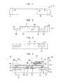
- a multiple-wafer assembly 180can be formed by electrically connecting the front conductive contacts 138 of one wafer 140 A with the rear contacts 168 of another wafer 140 B.
- the contacts 138 , 168can be joined through the RDL 170 with a bonding layer 174 between at least the RDL and the rear contacts 168 , the bonding layer 174 including a bond metal, e.g., tin, solder, conductive paste, anisotropic conductive adhesive or other conductive joining material.
- the contacts 138 , 168can be electrically connected together through another joining technique such as thermocompression bonding, diffusion bonding or other technique.
- FIG. 14illustrates a further stage in which a multi-wafer assembly 180 ( FIG. 13 ) can be severed along dicing lanes of the microelectronic elements, e.g., integrated circuit chips, therein to form a stacked microelectronic unit 182 which contains units 184 A, 184 B being severed portions of each wafer 140 A, 140 B ( FIG. 13 ).
- the microelectronic unit 182can now be electrically joined to a circuit panel 186 or to other circuit elements through the exposed front contacts 138 or RDL layer 170 and bond metal 188 .
- the microelectronic unit 182can be joined to a circuit panel in a similar manner by way of the rear contacts 168 of unit 184 A and a bond metal therebetween.
- a sacrificial layer 190 of materialsuch as a photoresist layer or other material is applied within the openings 154 and on the rear surface 114 . Openings are then formed in the sacrificial layer 190 which expose the polysilicon regions. Portions of the polysilicon regions, or the polysilicon material then can be completely removed through the openings in the sacrificial layer 190 , such as, for example, by etching the polysilicon in a manner which is selective relative to the other materials, e.g., the sacrificial layer 190 and a dielectric layer 122 which are exposed to the etchant.
- the sacrificial layer 190can be removed from the openings 154 and the rear surface 114 of the semiconductor region 100 , after which dielectric layer 192 ( FIG. 17 ) can be formed to overlie exposed surfaces of the semiconductor region 100 . Processing then resumes with the formation of a metal layer 166 as described above with respect to FIG. 10 .
- FIG. 18illustrates a variation of the above-described embodiment ( FIGS. 6-11 ) in which the opening which extends from the rear surface is a staged opening in which a first opening 204 extends from the rear surface 114 towards the front surface, and then a second opening 206 extends from within the first opening towards the front surface so as to expose the sacrificial region 220 .
- certain aspects of the openings and aspects of dielectric or conductive structures accompanying the openingscan be as described in U.S. application Ser. No. 12/072,508 filed Feb. 26, 2008 and Ser. No. 12/784,841 filed May 21, 2010, the disclosures of these applications being incorporated by reference herein.
- a maximum width 258 of the first openingis greater than a maximum width 260 of the second opening.
- the maximum width 260can be greater than a maximum width 262 of the conductive via which results after replacing the removed polysilicon material in region 220 with the metal as shown and described above with respect to FIG. 10 .
- the first opening 204can be tapered to become smaller in a direction towards the front surface, which is also in a direction towards the second opening 206 .
- the second opening 206can also be tapered to become smaller in a direction towards the front surface.
- a dielectric layer 264 which lines the first openingcan be the same layer or a different layer from the dielectric layer 266 which lines the second opening.
- a solder mask 270can overlie portions of the rear surface 114 , the rear contacts 168 being exposed within openings 272 of the solder mask.
- FIG. 19illustrates another variation of the above-described embodiment ( FIGS. 6-11 ) in which a conductive interconnect 274 extends along dielectric layer 264 and onto rear surface 114 where it electrically connects with the rear contact 268 .
- the rear contact 268can be formed integrally with the conductive interconnect 274 , e.g., as parts of the same metal layer or set of metal layers which are formed simultaneously on exposed surfaces 276 , 278 of the dielectric layer 264 within opening 254 and over the rear surface 114 .
- the conductive interconnectextends along a first wall 254 A of the opening, but not along a second wall 254 B thereof.
- the conductive interconnectcan conform to a contour of a wall 254 A of the opening 254 over which it lies.
- the conductive interconnect 274can be the only conductive element extending within the first opening and can extend from a single conductive via exposed thereto, e.g., through second opening 256 .
- the conductive interconnect 274 and other conductive interconnects 274can be provided as a plurality of conductive traces which overlie interior surfaces of a relatively large opening 254 to which a number of conductive vias 220 are exposed either directly or through corresponding second openings between the vias and the first opening.
- a microelectronic element 102 of the wafercan have more than one first opening therein.
- a plurality of conductive interconnects 374( FIG. 20 ) can extend along one or more interior surfaces of another first opening 354 which extends from the rear surface towards the front surface, the conductive interconnects 374 being electrically connected with rear contacts 368 overlying the rear surface. As illustrated in FIG.
- the conductive interconnects 274can extend in a directions which are up the sloped wall of the opening between the conductive vias and the rear contacts.
- one or more of the conductive interconnects, such as interconnects 274 A, 274 B,can extend in directions which are partly up the sloped wall and partly in a direction along the sloped wall.
- the conductive interconnectscan be formed in a manner such as the conductive elements, e.g., traces are formed as described in commonly owned U.S. application Ser. No. 12/842,669 filed Jul. 23, 2010, the disclosure of which is incorporated by reference herein.
- a single opening 454FIG.
- the integrated circuit chipcan be a dynamic random access memory (“DRAM”) chip having a plurality of conductive vias 420 to which the conductive interconnects 474 can be connected directly or indirectly by way of second openings, for example.
- DRAMdynamic random access memory
- some of the conductive interconnects 474can extend in a first direction 430 from conductive vias 420 , while other conductive interconnects 474 extend in a second direction 432 from conductive vias 420 .
- FIG. 22illustrates a particular variation in which the rear contact 568 is provided as a conductive pad overlying a region 590 of dielectric material which fills the opening 554 .
- the rear contact 568can be connected with the conductive via through a metal post which extends through an aperture 592 extending through the dielectric region 590 .
- a dielectric region 590is formed of polymeric material by filling the first opening. Then, an aperture can be formed in the dielectric region, such as by laser ablation, mechanical milling, or other technique. A metal layer then can be formed in the aperture to form the post 566 .
- the aperturecan have a wall 570 which extends in a vertical direction 510 , i.e., a normal direction with respect to the front surface 112 of the monocrystalline semiconductor region 100 .
- the post 566 formed thereinextends in the vertical direction 510 between the conductive via 520 and surface 593 on which a conductive contact 568 is provided.
- Such wall 570extends in a different direction from, and at an acute angle 512 with respect to the wall 552 of the opening 554 .
- the wall 570 of the aperturemight not extend in a vertical direction, but nevertheless extends at an acute angle 512 with respect to a direction in which the wall 552 of the opening 554 extends.
- the post 566can be a hollow tube-like structure having a central opening; in another embodiment, the post can be solid, i.e., without having an opening therein.
- a conductive padcan be formed atop the post as the rear contact. In another embodiment, the conductive pad can be omitted. In such case, the exposed end of the post can either extend above the surface 593 of the dielectric region, be co-planar with the surface 593 , or be recessed somewhat below the surface 593 .
- FIG. 23illustrates a variation of the embodiment illustrated in FIG. 19 , in which the polysilicon region 620 is not removed prior to forming the metal layer. Rather, the polysilicon region 620 is allowed to remain in place when a metal layer 668 is formed in contact therewith, the metal layer 668 forming at least a portion of a conductive interconnect which extends along a wall of the dielectric layer 664 and is electrically connected with the rear contact 670 .
- a portion 672 of the conductive interconnect which overlies the dielectric layer over the rear surface or within the first openingcan be formed integrally with the rear contact 670 .
- a plurality of conductive interconnectscan extend along one or more interior surfaces of an opening from a plurality of metal layers 668 connected to respective polysilicon regions 620 .
- the opening 654can be filled with a dielectric material 680 .
- the dielectric material 680can help to enhance mechanical strength of the structure, and may also provide insulation between respective conductive interconnects within an opening 654 .
- a portion of the polysiliconmay still remain therein.
- the remaining polysiliconmay fill a portion of region 720 adjacent to the front surface 112 of the monocrystalline semiconductor region 100 .
- the metal layer 768 formed thereoncontacts the polysilicon within the volume contained within the walls of the originally formed dielectric layer 770 .
- a conductive structureis provided which extends from the front surface 112 through a remaining polysilicon portion 720 of the original via, and through a metal portion 724 contained within the walls surrounding the original polysilicon portion.
- FIG. 25illustrates a further variation of the embodiment shown and described above relative to FIG. 19 in which the metal layer 868 within the second opening 856 conforms to a contour of the surface 870 of the second opening in the semiconductor region 100 .
- the metal layer 868can at least substantially cover, and can fully cover interior surfaces of the dielectric layer 872 within the second opening 856 .
- a via middle fabrication processdiffers from the above-described via first fabrication process in that high temperature processing used in forming the active circuit elements 924 ( FIG. 26 ) is performed before forming conductive vias 920 ( FIG. 27 ).
- the vias 920extend to a depth D 1 below the depth D 2 to which active circuit elements 924 extend.
- the conductive vias 920 of this embodimenttypically are formed after at least the high temperature processing used in forming the active circuit elements 924 is completed.
- the conductive vias 920can be formed before forming wiring elements of the wafer, e.g., metal wiring lines 936 and vias 937 which connect the wiring lines within one or more metallization levels of the wafer within dielectric region 934 and before forming the conductive contacts 938 , e.g., conductive pads, which are exposed at an exterior surface 942 of the wafer 940 .
- the vias 920do not need to withstand high temperature processing, they can be formed of a final metal.
- the vias 920can include a metal such as nickel, copper or aluminum.
- the vias 920can be formed by plating.
- the viascan include tungsten or titanium, and can be formed by a PVD or CVD process, or combination thereof, for example.
- the conductive viasextend from a height H 1 of a major surface 931 of a dielectric layer 932 above the front major surface 912 of the monocrystalline semiconductor region 100 , the vias extending to a depth D 1 which typically is below a depth D 2 to which the active circuit elements 924 extend.
- Further processingmay also be conducted to form a front RDL as described above relative to FIG. 12 .
- Processingcan also be performed according to particular variations described above with respect to FIGS. 13-14 , with respect to FIGS. 15-17 , FIG. 18 , FIGS. 19-20 , FIGS. 19 , 21 , FIG. 22 , or FIG. 25 .
- the metal within the conductive vias 920 of a via middle starting structurecan be copper, nickel or aluminum or a combination thereof.
- the vias and via conductorscan be formed by processes such as those disclosed in greater detail in the co-pending, commonly assigned United States Patent Applications titled “MICROELECTRONIC ELEMENTS HAVING METALLIC PADS OVELYING VIAS,” “METHOD OF FORMING SEMICONDUCTOR ELEMENTS USING MICRO-ABRASIVE PARTICLE STREAM,” “NON-LITHOGRAPHIC FORMATION OF THREE-DIMENSIONAL CONDUCTIVE ELEMENTS,” “ACTIVE CHIP ON CARRIER OR LAMINATED CHIP HAVING MICROELECTRONIC ELEMENT EMBEDDED THEREIN,” and “MICROELECTRONIC ELEMENTS WITH POST-ASSEMBLY PLANARIZATION” filed of even date herewith, and in published US Patent Application Publication No. 20080246136, the disclosures of which are incorporated by reference herein.
- a system 900 in accordance with a further embodiment of the inventionincludes a structure 906 as described above in conjunction with other electronic components 908 and 910 .
- component 908is a semiconductor chip whereas component 910 is a display screen, but any other components can be used.
- the structure 906 as described abovemay be, for example, a microelectronic unit 184 A or a stacked microelectronic assembly 182 as discussed above in connection with FIG. 14 , or any of FIGS. 18-27 , or a structure 184 A incorporating plural chips as discussed with reference to FIG. 14 . In a further variant, both may be provided, and any number of such structures may be used.
- Structure 906 and components 908 and 910are mounted in a common housing 901 , schematically depicted in broken lines, and are electrically interconnected with one another as necessary to form the desired circuit.
- the systemincludes a circuit panel 902 such as a flexible printed circuit board, and the circuit panel includes numerous conductors 904 , of which only one is depicted in FIG. 28 , interconnecting the components with one another.
- the housing 901is depicted as a portable housing of the type usable, for example, in a cellular telephone or personal digital assistant, and screen 910 is exposed at the surface of the housing.
- structure 906includes a light-sensitive element such as an imaging chip
- a lens 911 or other optical devicealso may be provided for routing light to the structure.
- FIG. 28the simplified system shown in FIG. 28 is merely exemplary; other systems, including systems commonly regarded as fixed structures, such as desktop computers, routers and the like can be made using the structures discussed above.
Landscapes
- Engineering & Computer Science (AREA)
- Microelectronics & Electronic Packaging (AREA)
- Power Engineering (AREA)
- Computer Hardware Design (AREA)
- Physics & Mathematics (AREA)
- Condensed Matter Physics & Semiconductors (AREA)
- General Physics & Mathematics (AREA)
- Manufacturing & Machinery (AREA)
- Internal Circuitry In Semiconductor Integrated Circuit Devices (AREA)
- Semiconductor Memories (AREA)
- Semiconductor Integrated Circuits (AREA)
Abstract
Description
| TABLE 1 | |||
| ECOAT NAME | POWERCRON 645 | POWERCRON 648 | CATHOGUARD 325 |
| MANUFACTURERS |
| MFG | PPG | PPG | BASF |
| TYPE | CATHODIC | CATHODIC | CATHODIC |
| POLYMER BASE | EPOXY | EPOXY | EPOXY |
| LOCATION | Pittsburgh, PA | Pittsburgh, PA | Southfield, MI |
| CURE | 20 min/149 C. | 20 min/175 C. | 20 min/175 C. |
| FILM PROPERTIES |
| COLOR | Clear (+dyed) | Black | Black |
| THICKNESS, μm | 10-35 | 10-35 | |
| PENCIL HARDNESS | 4H |
| BATH CHARACTERISTICS |
| SOLIDS, % wt. | 7.0 | (6.5-8.0) | 10-12 | 9-11 |
| pH (25 C) | 5.5-5.9 | 7-9 | 4.3 |
| CONDUCTIVITY (25 C.) μS | 450-600 | 500-800 | 400-800 |
| P/B RATIO | |||
| OPERATION TEMP., C. | 27-32 | 23-28 | 23-28 |
| TIME, sec | 60-120 | ||
| ANODE | SS316 | 316SS | 316SS |
| VOLTS | 40, max | 50-150 |
| APPLICATION DATA |
| Pb/Pf-free | Pb-free | Pb or Pb-free | Pb-free |
| HAPs, g/L | 60-84 | COMPLIANT | |
| VOC, g/L (MINUS WATER) | 60-84 | <95 | |
| CURE | 20 min/175 C. | 20 min/175 C. |
| FILM PROPERTIES |
| COLOR | Black | Black | Black |
| THICKNESS, μm | 10-35 | 10-38 | 13-36 |
| PENCIL HARDNESS | 2H+ | 4H |
| BATH CHARACTERISTICS |
| SOLIDS, % wt. | 20 | (18-22) | 20 | (19-21) | 17.0-21.0 |
| pH (25 C.) | 5.9 | (5.8-6.2) | 5.8 | (5.6-5.9) | 5.4-6.0 |
| CONDUCTIVITY (25 C.) μS | 1000-1500 | 1200-1500 | 1000-1700 |
| P/B RATIO | 0.12-0.14 | 0.12-0.16 | 0.15-0.20 |
| OPERATION TEMP., C. | 30-34 | 34 | 29-35 |
| TIME, sec | 120-180 | 60-180 | 120+ |
| ANODE | SS316 | SS316 | SS316 |
| VOLTS | 200-400 | >100 | |
| Pb/Pf-free | Pb-free | Pb-free | |
| HAPs, g/L | |||
| VOC, g/L (MINUS WATER) | |||
Claims (24)
Priority Applications (8)
| Application Number | Priority Date | Filing Date | Title |
|---|---|---|---|
| US12/842,651US8796135B2 (en) | 2010-07-23 | 2010-07-23 | Microelectronic elements with rear contacts connected with via first or via middle structures |
| CN201080069192.1ACN103109349B (en) | 2010-07-23 | 2010-10-13 | There is the microelectronic element with the back contact of the first path or via intermedia anatomical connectivity |
| BR112013001769ABR112013001769A2 (en) | 2010-07-23 | 2010-10-13 | microelectronic unit, system, and method of manufacturing a microelectronic unit. |
| KR1020137004576AKR101597341B1 (en) | 2010-07-23 | 2010-10-13 | Microelectronic elements with rear contacts connected with via first or via middle structures |
| EP10855116.9AEP2596520B1 (en) | 2010-07-23 | 2010-10-13 | Microelectronic elements with rear contacts connected with via first or via middle structures |
| PCT/US2010/052458WO2012011928A1 (en) | 2010-07-23 | 2010-10-13 | Microelectronic elements with rear contacts connected with via first or via middle structures |
| JP2013521757AJP5801889B2 (en) | 2010-07-23 | 2010-10-13 | Microelectronic device with back contact connected via via-first structure or via-mid structure |
| TW099140226ATWI502712B (en) | 2010-07-23 | 2010-11-22 | Microelectronic elements with rear contacts connected with via first or via middle structures |
Applications Claiming Priority (1)
| Application Number | Priority Date | Filing Date | Title |
|---|---|---|---|
| US12/842,651US8796135B2 (en) | 2010-07-23 | 2010-07-23 | Microelectronic elements with rear contacts connected with via first or via middle structures |
Publications (2)
| Publication Number | Publication Date |
|---|---|
| US20120018863A1 US20120018863A1 (en) | 2012-01-26 |
| US8796135B2true US8796135B2 (en) | 2014-08-05 |
Family
ID=45492916
Family Applications (1)
| Application Number | Title | Priority Date | Filing Date |
|---|---|---|---|
| US12/842,651Active2031-02-07US8796135B2 (en) | 2010-07-23 | 2010-07-23 | Microelectronic elements with rear contacts connected with via first or via middle structures |
Country Status (8)
| Country | Link |
|---|---|
| US (1) | US8796135B2 (en) |
| EP (1) | EP2596520B1 (en) |
| JP (1) | JP5801889B2 (en) |
| KR (1) | KR101597341B1 (en) |
| CN (1) | CN103109349B (en) |
| BR (1) | BR112013001769A2 (en) |
| TW (1) | TWI502712B (en) |
| WO (1) | WO2012011928A1 (en) |
Cited By (24)
| Publication number | Priority date | Publication date | Assignee | Title |
|---|---|---|---|---|
| US9355948B2 (en) | 2010-09-17 | 2016-05-31 | Tessera, Inc. | Multi-function and shielded 3D interconnects |
| US9627500B2 (en) | 2015-01-29 | 2017-04-18 | Samsung Electronics Co., Ltd. | Semiconductor device having work-function metal and method of forming the same |
| US9818668B2 (en) | 2014-03-07 | 2017-11-14 | Invensas Corporation | Thermal vias disposed in a substrate without a liner layer |
| US10170412B2 (en) | 2012-05-22 | 2019-01-01 | Invensas Corporation | Substrate-less stackable package with wire-bond interconnect |
| US10181457B2 (en) | 2015-10-26 | 2019-01-15 | Invensas Corporation | Microelectronic package for wafer-level chip scale packaging with fan-out |
| US10283445B2 (en) | 2016-10-26 | 2019-05-07 | Invensas Corporation | Bonding of laminates with electrical interconnects |
| US10290613B2 (en) | 2013-11-22 | 2019-05-14 | Invensas Corporation | Multiple bond via arrays of different wire heights on a same substrate |
| US10299368B2 (en) | 2016-12-21 | 2019-05-21 | Invensas Corporation | Surface integrated waveguides and circuit structures therefor |
| US10297582B2 (en) | 2012-08-03 | 2019-05-21 | Invensas Corporation | BVA interposer |
| US10325877B2 (en) | 2015-12-30 | 2019-06-18 | Invensas Corporation | Embedded wire bond wires for vertical integration with separate surface mount and wire bond mounting surfaces |
| US10332854B2 (en) | 2015-10-23 | 2019-06-25 | Invensas Corporation | Anchoring structure of fine pitch bva |
| US10381326B2 (en) | 2014-05-28 | 2019-08-13 | Invensas Corporation | Structure and method for integrated circuits packaging with increased density |
| US10460958B2 (en) | 2013-08-07 | 2019-10-29 | Invensas Corporation | Method of manufacturing embedded packaging with preformed vias |
| US10490528B2 (en) | 2015-10-12 | 2019-11-26 | Invensas Corporation | Embedded wire bond wires |
| US10529636B2 (en) | 2014-01-17 | 2020-01-07 | Invensas Corporation | Fine pitch BVA using reconstituted wafer with area array accessible for testing |
| US10559537B2 (en) | 2015-10-12 | 2020-02-11 | Invensas Corporation | Wire bond wires for interference shielding |
| US10593643B2 (en) | 2011-05-03 | 2020-03-17 | Tessera, Inc. | Package-on-package assembly with wire bonds to encapsulation surface |
| US10658302B2 (en) | 2016-07-29 | 2020-05-19 | Invensas Corporation | Wire bonding method and apparatus for electromagnetic interference shielding |
| US10756049B2 (en) | 2011-10-17 | 2020-08-25 | Invensas Corporation | Package-on-package assembly with wire bond vias |
| US10806036B2 (en) | 2015-03-05 | 2020-10-13 | Invensas Corporation | Pressing of wire bond wire tips to provide bent-over tips |
| US11164852B2 (en) | 2016-11-28 | 2021-11-02 | Taiwan Semiconductor Manufacturing Co., Ltd. | Method of forming package structure |
| US20230025859A1 (en)* | 2021-07-13 | 2023-01-26 | Changxin Memory Technologies, Inc. | Semiconductor structure and method for forming same |
| US12125784B2 (en) | 2018-10-22 | 2024-10-22 | Adeia Semiconductor Bonding Technologies Inc. | Interconnect structures |
| US12381128B2 (en) | 2020-12-28 | 2025-08-05 | Adeia Semiconductor Bonding Technologies Inc. | Structures with through-substrate vias and methods for forming the same |
Families Citing this family (92)
| Publication number | Priority date | Publication date | Assignee | Title |
|---|---|---|---|---|
| US8569876B2 (en) | 2006-11-22 | 2013-10-29 | Tessera, Inc. | Packaged semiconductor chips with array |
| US8405196B2 (en) | 2007-03-05 | 2013-03-26 | DigitalOptics Corporation Europe Limited | Chips having rear contacts connected by through vias to front contacts |
| WO2009017835A2 (en) | 2007-07-31 | 2009-02-05 | Tessera, Inc. | Semiconductor packaging process using through silicon vias |
| US8513119B2 (en) | 2008-12-10 | 2013-08-20 | Taiwan Semiconductor Manufacturing Company, Ltd. | Method of forming bump structure having tapered sidewalls for stacked dies |
| US20100171197A1 (en) | 2009-01-05 | 2010-07-08 | Hung-Pin Chang | Isolation Structure for Stacked Dies |
| US8304863B2 (en)* | 2010-02-09 | 2012-11-06 | International Business Machines Corporation | Electromigration immune through-substrate vias |
| US8466059B2 (en) | 2010-03-30 | 2013-06-18 | Taiwan Semiconductor Manufacturing Company, Ltd. | Multi-layer interconnect structure for stacked dies |
| US8796135B2 (en) | 2010-07-23 | 2014-08-05 | Tessera, Inc. | Microelectronic elements with rear contacts connected with via first or via middle structures |
| US8791575B2 (en) | 2010-07-23 | 2014-07-29 | Tessera, Inc. | Microelectronic elements having metallic pads overlying vias |
| US9640437B2 (en) | 2010-07-23 | 2017-05-02 | Tessera, Inc. | Methods of forming semiconductor elements using micro-abrasive particle stream |
| US8598695B2 (en) | 2010-07-23 | 2013-12-03 | Tessera, Inc. | Active chip on carrier or laminated chip having microelectronic element embedded therein |
| US8847380B2 (en) | 2010-09-17 | 2014-09-30 | Tessera, Inc. | Staged via formation from both sides of chip |
| US8736066B2 (en) | 2010-12-02 | 2014-05-27 | Tessera, Inc. | Stacked microelectronic assemby with TSVS formed in stages and carrier above chip |
| US8637968B2 (en) | 2010-12-02 | 2014-01-28 | Tessera, Inc. | Stacked microelectronic assembly having interposer connecting active chips |
| US8587126B2 (en) | 2010-12-02 | 2013-11-19 | Tessera, Inc. | Stacked microelectronic assembly with TSVs formed in stages with plural active chips |
| US8610264B2 (en) | 2010-12-08 | 2013-12-17 | Tessera, Inc. | Compliant interconnects in wafers |
| US8742541B2 (en) | 2010-12-09 | 2014-06-03 | Tessera, Inc. | High density three-dimensional integrated capacitors |
| US8502340B2 (en) | 2010-12-09 | 2013-08-06 | Tessera, Inc. | High density three-dimensional integrated capacitors |
| US8486758B2 (en) | 2010-12-20 | 2013-07-16 | Tessera, Inc. | Simultaneous wafer bonding and interconnect joining |
| US8841765B2 (en) | 2011-04-22 | 2014-09-23 | Tessera, Inc. | Multi-chip module with stacked face-down connected dies |
| US8975751B2 (en) | 2011-04-22 | 2015-03-10 | Tessera, Inc. | Vias in porous substrates |
| JP5541233B2 (en)* | 2011-06-06 | 2014-07-09 | Tdk株式会社 | Manufacturing method of semiconductor chip |
| US8723049B2 (en) | 2011-06-09 | 2014-05-13 | Tessera, Inc. | Low-stress TSV design using conductive particles |
| US8900994B2 (en) | 2011-06-09 | 2014-12-02 | Taiwan Semiconductor Manufacturing Company, Ltd. | Method for producing a protective structure |
| US8546951B2 (en) | 2011-06-09 | 2013-10-01 | Optiz, Inc. | 3D integration microelectronic assembly for integrated circuit devices |
| US8552518B2 (en) | 2011-06-09 | 2013-10-08 | Optiz, Inc. | 3D integrated microelectronic assembly with stress reducing interconnects |
| US8546900B2 (en) | 2011-06-09 | 2013-10-01 | Optiz, Inc. | 3D integration microelectronic assembly for integrated circuit devices |
| US8513817B2 (en) | 2011-07-12 | 2013-08-20 | Invensas Corporation | Memory module in a package |
| US8502390B2 (en) | 2011-07-12 | 2013-08-06 | Tessera, Inc. | De-skewed multi-die packages |
| US8823165B2 (en) | 2011-07-12 | 2014-09-02 | Invensas Corporation | Memory module in a package |
| US8604576B2 (en)* | 2011-07-19 | 2013-12-10 | Opitz, Inc. | Low stress cavity package for back side illuminated image sensor, and method of making same |
| US9018725B2 (en) | 2011-09-02 | 2015-04-28 | Optiz, Inc. | Stepped package for image sensor and method of making same |
| KR101894823B1 (en) | 2011-10-03 | 2018-09-04 | 인벤사스 코포레이션 | Stub minimization for multi-die wirebond assemblies with parallel windows |
| US8405207B1 (en) | 2011-10-03 | 2013-03-26 | Invensas Corporation | Stub minimization for wirebond assemblies without windows |
| US8436477B2 (en) | 2011-10-03 | 2013-05-07 | Invensas Corporation | Stub minimization using duplicate sets of signal terminals in assemblies without wirebonds to package substrate |
| JP5947904B2 (en) | 2011-10-03 | 2016-07-06 | インヴェンサス・コーポレイション | Stub minimization for multi-die wirebond assemblies with orthogonal windows |
| TWI515864B (en) | 2011-10-03 | 2016-01-01 | 英帆薩斯公司 | Stub minimization with terminal grids offset from center of package |
| US8345441B1 (en) | 2011-10-03 | 2013-01-01 | Invensas Corporation | Stub minimization for multi-die wirebond assemblies with parallel windows |
| US8653646B2 (en) | 2011-10-03 | 2014-02-18 | Invensas Corporation | Stub minimization using duplicate sets of terminals for wirebond assemblies without windows |
| US8441111B2 (en) | 2011-10-03 | 2013-05-14 | Invensas Corporation | Stub minimization for multi-die wirebond assemblies with parallel windows |
| US8436457B2 (en) | 2011-10-03 | 2013-05-07 | Invensas Corporation | Stub minimization for multi-die wirebond assemblies with parallel windows |
| US8525327B2 (en) | 2011-10-03 | 2013-09-03 | Invensas Corporation | Stub minimization for assemblies without wirebonds to package substrate |
| JP5802515B2 (en)* | 2011-10-19 | 2015-10-28 | 株式会社東芝 | Semiconductor device and manufacturing method thereof |
| US8796800B2 (en) | 2011-11-21 | 2014-08-05 | Optiz, Inc. | Interposer package for CMOS image sensor and method of making same |
| US8432011B1 (en) | 2011-12-06 | 2013-04-30 | Optiz, Inc. | Wire bond interposer package for CMOS image sensor and method of making same |
| US8570669B2 (en) | 2012-01-23 | 2013-10-29 | Optiz, Inc | Multi-layer polymer lens and method of making same |
| US8692344B2 (en) | 2012-03-16 | 2014-04-08 | Optiz, Inc | Back side illuminated image sensor architecture, and method of making same |
| US9233511B2 (en) | 2012-05-10 | 2016-01-12 | Optiz, Inc. | Method of making stamped multi-layer polymer lens |
| US8921759B2 (en) | 2012-07-26 | 2014-12-30 | Optiz, Inc. | Integrated image sensor package with liquid crystal lens |
| US9117820B2 (en)* | 2012-08-08 | 2015-08-25 | United Microelectronics Corp. | Conductive line of semiconductor device |
| US8846447B2 (en) | 2012-08-23 | 2014-09-30 | Invensas Corporation | Thin wafer handling and known good die test method |
| US8787034B2 (en) | 2012-08-27 | 2014-07-22 | Invensas Corporation | Co-support system and microelectronic assembly |
| US9368477B2 (en) | 2012-08-27 | 2016-06-14 | Invensas Corporation | Co-support circuit panel and microelectronic packages |
| US8848391B2 (en) | 2012-08-27 | 2014-09-30 | Invensas Corporation | Co-support component and microelectronic assembly |
| US8848392B2 (en) | 2012-08-27 | 2014-09-30 | Invensas Corporation | Co-support module and microelectronic assembly |
| CN103681460A (en)* | 2012-09-05 | 2014-03-26 | 欣兴电子股份有限公司 | Electronic component manufacturing method |
| US8759930B2 (en) | 2012-09-10 | 2014-06-24 | Optiz, Inc. | Low profile image sensor package |
| US8963335B2 (en) | 2012-09-13 | 2015-02-24 | Invensas Corporation | Tunable composite interposer |
| US9076785B2 (en) | 2012-12-11 | 2015-07-07 | Invensas Corporation | Method and structures for via substrate repair and assembly |
| US9219091B2 (en) | 2013-03-12 | 2015-12-22 | Optiz, Inc. | Low profile sensor module and method of making same |
| US9190443B2 (en) | 2013-03-12 | 2015-11-17 | Optiz Inc. | Low profile image sensor |
| US9142695B2 (en) | 2013-06-03 | 2015-09-22 | Optiz, Inc. | Sensor package with exposed sensor array and method of making same |
| US9070423B2 (en) | 2013-06-11 | 2015-06-30 | Invensas Corporation | Single package dual channel memory with co-support |
| US20150021773A1 (en)* | 2013-07-22 | 2015-01-22 | Conversant Intellectual Property Management Inc. | Through Semiconductor via Structure with Reduced Stress Proximity Effect |
| US9496247B2 (en) | 2013-08-26 | 2016-11-15 | Optiz, Inc. | Integrated camera module and method of making same |
| US9461190B2 (en) | 2013-09-24 | 2016-10-04 | Optiz, Inc. | Low profile sensor package with cooling feature and method of making same |
| US20150097228A1 (en)* | 2013-10-07 | 2015-04-09 | Nanya Technology Corporation | Method for manufacturing semiconductor device |
| US9123555B2 (en) | 2013-10-25 | 2015-09-01 | Invensas Corporation | Co-support for XFD packaging |
| US9496297B2 (en) | 2013-12-05 | 2016-11-15 | Optiz, Inc. | Sensor package with cooling feature and method of making same |
| US9667900B2 (en) | 2013-12-09 | 2017-05-30 | Optiz, Inc. | Three dimensional system-on-chip image sensor package |
| KR102107037B1 (en)* | 2014-02-21 | 2020-05-07 | 삼성전기주식회사 | Printed circuit board and method of manufacturing the same |
| US9985063B2 (en) | 2014-04-22 | 2018-05-29 | Optiz, Inc. | Imaging device with photo detectors and color filters arranged by color transmission characteristics and absorption coefficients |
| US9524917B2 (en) | 2014-04-23 | 2016-12-20 | Optiz, Inc. | Chip level heat dissipation using silicon |
| US9281296B2 (en) | 2014-07-31 | 2016-03-08 | Invensas Corporation | Die stacking techniques in BGA memory package for small footprint CPU and memory motherboard design |
| US9666730B2 (en) | 2014-08-18 | 2017-05-30 | Optiz, Inc. | Wire bond sensor package |
| US9633953B2 (en)* | 2014-09-04 | 2017-04-25 | Apple Inc. | Methodology to achieve zero warpage for IC package |
| US9691437B2 (en) | 2014-09-25 | 2017-06-27 | Invensas Corporation | Compact microelectronic assembly having reduced spacing between controller and memory packages |
| US9543347B2 (en) | 2015-02-24 | 2017-01-10 | Optiz, Inc. | Stress released image sensor package structure and method |
| NZ773836A (en)* | 2015-03-16 | 2022-07-01 | Magic Leap Inc | Methods and systems for diagnosing and treating health ailments |
| CN108370109A (en)* | 2015-09-01 | 2018-08-03 | R&D电路股份有限公司 | Interconnects with traces anywhere |
| US9484080B1 (en) | 2015-11-09 | 2016-11-01 | Invensas Corporation | High-bandwidth memory application with controlled impedance loading |
| US9679613B1 (en) | 2016-05-06 | 2017-06-13 | Invensas Corporation | TFD I/O partition for high-speed, high-density applications |
| US9996725B2 (en) | 2016-11-03 | 2018-06-12 | Optiz, Inc. | Under screen sensor assembly |
| JP6472931B1 (en)* | 2017-11-10 | 2019-02-20 | 新電元工業株式会社 | Electronic module |
| KR102467030B1 (en)* | 2018-01-17 | 2022-11-14 | 삼성전자주식회사 | Semiconductor package and semiconductor apparatus comprising the same |
| DE102018210815A1 (en) | 2018-06-30 | 2020-01-02 | Robert Bosch Gmbh | Electrical contacting, method for producing electrical contacting, system |
| MY201172A (en)* | 2018-09-19 | 2024-02-08 | Intel Corp | Stacked through-silicon vias for multi-device packages |
| US20200105646A1 (en)* | 2018-10-01 | 2020-04-02 | Nanya Technology Corporation | Semiconductor structure having through silicon via structure and method for forming the same |
| US11408589B2 (en) | 2019-12-05 | 2022-08-09 | Optiz, Inc. | Monolithic multi-focus light source device |
| US20210335660A1 (en)* | 2020-04-24 | 2021-10-28 | Nanya Technology Corporation | Semiconductor structure having void between bonded wafers and manufacturing method tehreof |
| US20220028758A1 (en)* | 2020-07-23 | 2022-01-27 | Qualcomm Incorporated | Backside power distribution network (pdn) processing |
| CN114038805A (en)* | 2021-11-24 | 2022-02-11 | 苏州科阳半导体有限公司 | Packaging structure and packaging method of semiconductor chip |
Citations (238)
| Publication number | Priority date | Publication date | Assignee | Title |
|---|---|---|---|---|
| US4074342A (en) | 1974-12-20 | 1978-02-14 | International Business Machines Corporation | Electrical package for lsi devices and assembly process therefor |
| US4682074A (en) | 1984-11-28 | 1987-07-21 | U.S. Philips Corporation | Electron-beam device and semiconductor device for use in such an electron-beam device |
| US4765864A (en) | 1987-07-15 | 1988-08-23 | Sri International | Etching method for producing an electrochemical cell in a crystalline substrate |
| EP0316799A1 (en) | 1987-11-13 | 1989-05-24 | Nissan Motor Co., Ltd. | Semiconductor device |
| US5229647A (en) | 1991-03-27 | 1993-07-20 | Micron Technology, Inc. | High density data storage using stacked wafers |
| US5322816A (en) | 1993-01-19 | 1994-06-21 | Hughes Aircraft Company | Method for forming deep conductive feedthroughs |
| US5481133A (en) | 1994-03-21 | 1996-01-02 | United Microelectronics Corporation | Three-dimensional multichip package |
| US5686762A (en) | 1995-12-21 | 1997-11-11 | Micron Technology, Inc. | Semiconductor device with improved bond pads |
| US5700735A (en) | 1996-08-22 | 1997-12-23 | Taiwan Semiconductor Manufacturing Company, Ltd. | Method of forming bond pad structure for the via plug process |
| US5703408A (en) | 1995-04-10 | 1997-12-30 | United Microelectronics Corporation | Bonding pad structure and method thereof |
| US5808874A (en) | 1996-05-02 | 1998-09-15 | Tessera, Inc. | Microelectronic connections with liquid conductive elements |
| EP0926723A1 (en) | 1997-11-26 | 1999-06-30 | STMicroelectronics S.r.l. | Process for forming front-back through contacts in micro-integrated electronic devices |
| US6005466A (en) | 1994-07-29 | 1999-12-21 | Mitel Semiconductor Limited | Trimmable inductor structure |
| KR19990088037A (en) | 1998-05-04 | 1999-12-27 | 루센트 테크놀러지스 인크 | Bond pad design for integrated circuits |
| US6013948A (en) | 1995-11-27 | 2000-01-11 | Micron Technology, Inc. | Stackable chip scale semiconductor package with mating contacts on opposed surfaces |
| US6022758A (en) | 1994-07-10 | 2000-02-08 | Shellcase Ltd. | Process for manufacturing solder leads on a semiconductor device package |
| US6031274A (en) | 1996-10-11 | 2000-02-29 | Hamamatsu Photonics K.K. | Back irradiation type light-receiving device and method of making the same |
| US6037668A (en) | 1998-11-13 | 2000-03-14 | Motorola, Inc. | Integrated circuit having a support structure |
| US6103552A (en) | 1998-08-10 | 2000-08-15 | Lin; Mou-Shiung | Wafer scale packaging scheme |
| US6143396A (en) | 1997-05-01 | 2000-11-07 | Texas Instruments Incorporated | System and method for reinforcing a bond pad |
| US6143369A (en) | 1996-01-12 | 2000-11-07 | Matsushita Electric Works, Ltd. | Process of impregnating substrate and impregnated substrate |
| US6169319B1 (en) | 1999-08-12 | 2001-01-02 | Tower Semiconductor Ltd. | Backside illuminated image sensor |
| US6181016B1 (en) | 1999-06-08 | 2001-01-30 | Winbond Electronics Corp | Bond-pad with a single anchoring structure |
| JP2001085559A (en) | 1999-09-10 | 2001-03-30 | Dainippon Printing Co Ltd | Semiconductor device and manufacturing method thereof |
| US6261865B1 (en) | 1998-10-06 | 2001-07-17 | Micron Technology, Inc. | Multi chip semiconductor package and method of construction |
| JP2001217386A (en) | 2000-02-03 | 2001-08-10 | Seiko Epson Corp | Semiconductor device, method of manufacturing the same, and electronic device |
| US6277669B1 (en) | 1999-09-15 | 2001-08-21 | Industrial Technology Research Institute | Wafer level packaging method and packages formed |
| US6284563B1 (en) | 1995-10-31 | 2001-09-04 | Tessera, Inc. | Method of making compliant microelectronic assemblies |
| US6313540B1 (en) | 1998-12-25 | 2001-11-06 | Nec Corporation | Electrode structure of semiconductor element |
| US20010048591A1 (en) | 1997-11-25 | 2001-12-06 | Joseph Fjelstad | Microelectronics component with rigid interposer |
| JP2002016178A (en) | 1999-10-29 | 2002-01-18 | Hitachi Ltd | Semiconductor device and method of manufacturing the same |
| US6362529B1 (en) | 1999-10-26 | 2002-03-26 | Sharp Kabushiki Kaisha | Stacked semiconductor device |
| US6368410B1 (en) | 1999-06-28 | 2002-04-09 | General Electric Company | Semiconductor processing article |
| US20020061723A1 (en) | 2000-11-17 | 2002-05-23 | Duescher Wayne O. | Raised island abrasive and process of manufacture |
| US6399892B1 (en) | 2000-09-19 | 2002-06-04 | International Business Machines Corporation | CTE compensated chip interposer |
| JP2002162212A (en) | 2000-11-24 | 2002-06-07 | Foundation Of River & Basin Integrated Communications Japan | Embankment strain measurement sensor |
| US20020096787A1 (en) | 1994-12-29 | 2002-07-25 | Tessera, Inc. | Connection components with posts |
| JP2002217331A (en) | 2000-10-23 | 2002-08-02 | Matsushita Electric Ind Co Ltd | Semiconductor chip, wiring board, manufacturing method thereof, and semiconductor device |
| US20020109236A1 (en) | 2001-02-09 | 2002-08-15 | Samsung Electronics Co., Ltd. | Three-dimensional multi-chip package having chip selection pads and manufacturing method thereof |
| US20020151171A1 (en) | 2001-03-28 | 2002-10-17 | Seiko Epson Corporation | Semiconductor device and manufacturing method therefor, circuit substrate, and electronic apparatus |
| US6472247B1 (en) | 2000-06-26 | 2002-10-29 | Ricoh Company, Ltd. | Solid-state imaging device and method of production of the same |
| US6492201B1 (en) | 1998-07-10 | 2002-12-10 | Tessera, Inc. | Forming microelectronic connection components by electrophoretic deposition |
| US6498387B1 (en) | 2000-02-15 | 2002-12-24 | Wen-Ken Yang | Wafer level package and the process of the same |
| US6498381B2 (en) | 2001-02-22 | 2002-12-24 | Tru-Si Technologies, Inc. | Semiconductor structures having multiple conductive layers in an opening, and methods for fabricating same |
| JP2002373957A (en) | 2001-06-14 | 2002-12-26 | Shinko Electric Ind Co Ltd | Semiconductor device and its manufacturing method |
| US6507113B1 (en) | 1999-11-19 | 2003-01-14 | General Electric Company | Electronic interface structures and methods of fabrication |
| US20030059976A1 (en) | 2001-09-24 | 2003-03-27 | Nathan Richard J. | Integrated package and methods for making same |
| US20030071331A1 (en) | 2001-10-17 | 2003-04-17 | Yoshihide Yamaguchi | Semiconductor device and structure for mounting the same |
| US6586955B2 (en) | 2000-03-13 | 2003-07-01 | Tessera, Inc. | Methods and structures for electronic probing arrays |
| US6608377B2 (en) | 2001-01-30 | 2003-08-19 | Samsung Electronics Co., Ltd. | Wafer level package including ground metal layer |
| US20030178714A1 (en) | 2002-03-20 | 2003-09-25 | Fujitsu Limited | Semiconductor device having a built-in contact-type sensor and manufacturing method thereof |
| US6638352B2 (en) | 2001-07-10 | 2003-10-28 | Hitachi, Ltd. | Thermal stable low elastic modulus material and device using the same |
| JP2003318178A (en) | 2002-04-24 | 2003-11-07 | Seiko Epson Corp | Semiconductor device and its manufacturing method, circuit board, and electronic equipment |
| US20040017012A1 (en) | 2000-10-23 | 2004-01-29 | Yuichiro Yamada | Semiconductor chip, wiring board and manufacturing process thereof as well as semiconductor device |
| US20040043607A1 (en) | 2002-08-29 | 2004-03-04 | Farnworth Warren M. | Methods for creating electrophoretically insulated vias in semiconductive substrates and resulting structures |
| US20040051173A1 (en) | 2001-12-10 | 2004-03-18 | Koh Philip Joseph | High frequency interconnect system using micromachined plugs and sockets |
| US20040061238A1 (en) | 2002-09-30 | 2004-04-01 | Kabushiki Kaisha Toshiba | Semiconductor device and method of manufacturing the same |
| US6716737B2 (en)* | 2002-07-29 | 2004-04-06 | Hewlett-Packard Development Company, L.P. | Method of forming a through-substrate interconnect |
| US6727576B2 (en) | 2001-10-31 | 2004-04-27 | Infineon Technologies Ag | Transfer wafer level packaging |
| TW200406884A (en) | 2002-10-30 | 2004-05-01 | Intelligent Sources Dev Corp | Method of forming a stacked-gate cell structure and its NAND-type flash memory array |
| US6737300B2 (en) | 2001-01-24 | 2004-05-18 | Advanced Semiconductor Engineering, Inc. | Chip scale package and manufacturing method |
| US6743660B2 (en) | 2002-01-12 | 2004-06-01 | Taiwan Semiconductor Manufacturing Co., Ltd | Method of making a wafer level chip scale package |
| US20040104454A1 (en) | 2002-10-10 | 2004-06-03 | Rohm Co., Ltd. | Semiconductor device and method of producing the same |
| JP2004165602A (en) | 2002-09-24 | 2004-06-10 | Hamamatsu Photonics Kk | Semiconductor device and its manufacturing method |
| JP2004200547A (en) | 2002-12-20 | 2004-07-15 | Seiko Epson Corp | Semiconductor chip, semiconductor wafer, semiconductor device and manufacturing method thereof, circuit board, and electronic equipment |
| KR20040066018A (en) | 2003-01-15 | 2004-07-23 | 세이코 엡슨 가부시키가이샤 | Semiconductor chip, semiconductor wafer, semiconductor device and method of manufacturing the same, circuit board, and electronic instrument |
| US20040155354A1 (en) | 2000-06-02 | 2004-08-12 | Seiko Epson Corporation | Semiconductor device, method of fabricating the same, stack-type semiconductor device, circuit board and electronic instrument |
| US20040173891A1 (en) | 2003-03-07 | 2004-09-09 | Ngk Spark Plug Co., Ltd. | Intermediate board, intermediate board with a semiconductor device, substrate board with an intermediate board, structural member including a semiconductor device, an intermediate board and a substrate board, and method of producing an intermediate board |
| US20040178495A1 (en) | 2003-03-14 | 2004-09-16 | Yean Tay Wuu | Microelectronic devices and methods for packaging microelectronic devices |
| US20040188819A1 (en) | 2003-03-31 | 2004-09-30 | Farnworth Warren M. | Wafer level methods for fabricating multi-dice chip scale semiconductor components |
| US6812549B2 (en) | 2001-03-07 | 2004-11-02 | Seiko Epson Corporation | Wiring board and fabricating method thereof, semiconductor device and fabricating method thereof, circuit board and electronic instrument |
| US20040217483A1 (en) | 2003-04-30 | 2004-11-04 | Infineon Technologies Ag | Semiconductor device and method for fabricating the semiconductor device |
| US20040222508A1 (en) | 2003-03-18 | 2004-11-11 | Akiyoshi Aoyagi | Semiconductor device, electronic device, electronic apparatus, method of manufacturing semiconductor device, and method of manufacturing electronic device |
| EP1482553A2 (en) | 2003-05-26 | 2004-12-01 | Sanyo Electric Co., Ltd. | Semiconductor device and manufacturing method thereof |
| US6828175B2 (en) | 2002-08-29 | 2004-12-07 | Micron Technology, Inc. | Semiconductor component with backside contacts and method of fabrication |
| US20040251525A1 (en) | 2003-06-16 | 2004-12-16 | Shellcase Ltd. | Methods and apparatus for packaging integrated circuit devices |
| US20040259292A1 (en) | 2003-04-03 | 2004-12-23 | Eric Beyne | Method for producing electrical through hole interconnects and devices made thereof |
| WO2004114397A1 (en) | 2003-06-20 | 2004-12-29 | Koninklijke Philips Electronics N.V. | Electronic device, assembly and methods of manufacturing an electronic device |
| US20050012225A1 (en) | 2002-11-15 | 2005-01-20 | Choi Seung-Yong | Wafer-level chip scale package and method for fabricating and using the same |
| JP2005026405A (en) | 2003-07-01 | 2005-01-27 | Sharp Corp | Through electrode structure and manufacturing method thereof, semiconductor chip and multichip semiconductor device |
| US20050046002A1 (en) | 2003-08-26 | 2005-03-03 | Kang-Wook Lee | Chip stack package and manufacturing method thereof |
| US6864172B2 (en) | 2002-06-18 | 2005-03-08 | Sanyo Electric Co., Ltd. | Manufacturing method of semiconductor device |
| US20050051883A1 (en) | 2003-06-19 | 2005-03-10 | Seiko Epson Corporation | Semiconductor device and method of manufacturing the same, circuit board, and electronic instrument |
| US6867123B2 (en) | 2001-02-08 | 2005-03-15 | Renesas Technology Corp. | Semiconductor integrated circuit device and its manufacturing method |
| US20050056903A1 (en) | 2003-08-28 | 2005-03-17 | Satoshi Yamamoto | Semiconductor package and method of manufacturing same |
| EP1519410A1 (en) | 2003-09-25 | 2005-03-30 | Interuniversitair Microelektronica Centrum vzw ( IMEC) | Method for producing electrical through hole interconnects and devices made thereof |
| JP2005093486A (en) | 2003-09-12 | 2005-04-07 | Seiko Epson Corp | Semiconductor device manufacturing method and semiconductor device |
| US6879049B1 (en) | 1998-01-23 | 2005-04-12 | Rohm Co., Ltd. | Damascene interconnection and semiconductor device |
| JP2005101268A (en) | 2003-09-25 | 2005-04-14 | Sanyo Electric Co Ltd | Method for manufacturing semiconductor device |
| US20050099259A1 (en) | 2003-09-30 | 2005-05-12 | Harris Edward B. | Inductor formed in an integrated circuit |
| TW200522274A (en) | 2003-12-26 | 2005-07-01 | Intelligent Sources Dev Corp | Paired stack-gate flash cell structure and its contactless nand-type flash memory arrays |
| US6914336B2 (en) | 2000-01-25 | 2005-07-05 | Nec Electronics Corporation | Semiconductor device structure and method for manufacturing the same |
| EP1551060A1 (en) | 2002-09-24 | 2005-07-06 | Hamamatsu Photonics K. K. | Photodiode array and method for manufacturing same |
| US20050148160A1 (en) | 2002-03-06 | 2005-07-07 | Farnworth Warren M. | Encapsulated semiconductor components and methods of fabrication |
| US20050156330A1 (en) | 2004-01-21 | 2005-07-21 | Harris James M. | Through-wafer contact to bonding pad |
| JP2005209967A (en) | 2004-01-23 | 2005-08-04 | Sharp Corp | Semiconductor device, module for optical device, and method for manufacturing semiconductor device |
| US6927156B2 (en) | 2003-06-18 | 2005-08-09 | Intel Corporation | Apparatus and method extending flip-chip pad structures for wirebonding on low-k dielectric silicon |
| JP2005216921A (en) | 2004-01-27 | 2005-08-11 | Hitachi Maxell Ltd | Metal mask for manufacturing semiconductor device and method for manufacturing semiconductor device |
| TW200535435A (en) | 2004-03-29 | 2005-11-01 | Applied Materials Inc | High throughput measurement of via defects in interconnects |
| US20050248002A1 (en) | 2004-05-07 | 2005-11-10 | Michael Newman | Fill for large volume vias |
| US20050260794A1 (en) | 2002-09-03 | 2005-11-24 | Industrial Technology Research Institute | Method for fabrication of wafer level package incorporating dual compliant layers |
| US20050279916A1 (en) | 2004-05-03 | 2005-12-22 | Tessera, Inc. | Image sensor package and fabrication method |
| US20050282374A1 (en) | 2004-06-22 | 2005-12-22 | Samsung Electronics Co., Ltd. | Method of forming a thin wafer stack for a wafer level package |
| US20050287783A1 (en) | 2004-06-29 | 2005-12-29 | Kirby Kyle K | Microelectronic devices and methods for forming interconnects in microelectronic devices |
| US6982475B1 (en) | 1998-03-20 | 2006-01-03 | Mcsp, Llc | Hermetic wafer scale integrated circuit structure |
| US20060001179A1 (en) | 2004-06-30 | 2006-01-05 | Shinko Electric Industries Co., Ltd. | Interposer, method of fabricating the same, and semiconductor device using the same |
| US20060001174A1 (en) | 2004-06-30 | 2006-01-05 | Nec Electronics Corporation | Semiconductor device and method for manufacturing the same |
| EP1619722A1 (en) | 2003-04-16 | 2006-01-25 | Hamamatsu Photonics K. K. | Method for manufacturing backside-illuminated optical sensor |
| US20060017161A1 (en) | 2004-07-22 | 2006-01-26 | Jae-Sik Chung | Semiconductor package having protective layer for re-routing lines and method of manufacturing the same |
| US20060046471A1 (en) | 2004-08-27 | 2006-03-02 | Kirby Kyle K | Methods for forming vias of varying lateral dimensions and semiconductor components and assemblies including same |
| US20060046348A1 (en) | 2004-09-01 | 2006-03-02 | Kang Byoung Y | Semiconductor chip packages and methods for fabricating the same |
| US20060046463A1 (en) | 2004-08-24 | 2006-03-02 | Watkins Charles M | Method of forming vias in semiconductor substrates without damaging active regions thereof and resulting structures |
| US20060043598A1 (en) | 2004-08-31 | 2006-03-02 | Kirby Kyle K | Methods of manufacture of a via structure comprising a plurality of conductive elements, semiconductor die, multichip module, and system including same |
| US20060055050A1 (en) | 2004-09-10 | 2006-03-16 | Hideo Numata | Semiconductor device and manufacturing method thereof |
| US20060068580A1 (en) | 2004-09-28 | 2006-03-30 | Sharp Kabushiki Kaisha | Semiconductor device and fabrication method thereof |
| US20060071347A1 (en) | 2004-10-04 | 2006-04-06 | Sharp Kabushiki Kaisha | Semiconductor device and fabrication method thereof |
| CN1758430A (en) | 2004-09-10 | 2006-04-12 | 株式会社东芝 | Semiconductor device and manufacturing method thereof |
| US20060079019A1 (en) | 2004-10-08 | 2006-04-13 | Easetech Korea Co., Ltd. | Method for manufacturing wafer level chip scale package using redistribution substrate |
| US20060076019A1 (en) | 2004-10-08 | 2006-04-13 | Ric Investments, Llc. | User interface having a pivotable coupling |
| EP1653510A2 (en) | 2004-10-28 | 2006-05-03 | Sanyo Electric Co., Ltd. | Semiconductor device and manufacturing method of the same |
| EP1653521A1 (en) | 2003-07-29 | 2006-05-03 | Hamamatsu Photonics K.K. | Backside-illuminated photodetector and method for manufacturing same |
| US20060094231A1 (en) | 2004-10-28 | 2006-05-04 | Lane Ralph L | Method of creating a tapered via using a receding mask and resulting structure |
| US20060115932A1 (en) | 1997-12-18 | 2006-06-01 | Farnworth Warren M | Method for fabricating semiconductor components with conductive vias |
| EP1686627A1 (en) | 2005-01-28 | 2006-08-02 | Samsung Electro-Mechanics Co., Ltd. | Semiconductor package and method of manufacturing the same |
| US20060175697A1 (en) | 2005-02-02 | 2006-08-10 | Tetsuya Kurosawa | Semiconductor device having semiconductor chips stacked and mounted thereon and manufacturing method thereof |
| US7091062B2 (en) | 2003-10-15 | 2006-08-15 | Infineon Technologies Ag | Wafer level packages for chips with sawn edge protection |
| US20060197217A1 (en) | 2005-03-02 | 2006-09-07 | Advanced Semiconductor Engineering, Inc. | Semiconductor package structure and method for manufacturing the same |
| US20060197216A1 (en) | 2005-03-02 | 2006-09-07 | Advanced Semiconductor Engineering, Inc. | Semiconductor package structure and method for manufacturing the same |
| US7112874B2 (en) | 2002-05-20 | 2006-09-26 | Imagerlabs, Inc. | Forming a multi segment integrated circuit with isolated substrates |
| US20060264029A1 (en) | 2005-05-23 | 2006-11-23 | Intel Corporation | Low inductance via structures |
| US20060278997A1 (en) | 2004-12-01 | 2006-12-14 | Tessera, Inc. | Soldered assemblies and methods of making the same |
| US20060292866A1 (en) | 2005-06-23 | 2006-12-28 | Borwick Robert L | Low temperature method for fabricating high-aspect ratio vias and devices fabricated by said method |
| US20070035020A1 (en) | 2004-12-20 | 2007-02-15 | Sanyo Electric Co., Ltd. | Semiconductor Apparatus and Semiconductor Module |
| JP2007053149A (en) | 2005-08-16 | 2007-03-01 | Renesas Technology Corp | Semiconductor wafer and its manufacturing method |
| US20070045779A1 (en) | 2005-09-01 | 2007-03-01 | Hiatt W M | Methods for forming through-wafer interconnects, intermediate structures so formed, and devices and systems having at least one solder dam structure |
| US20070052050A1 (en) | 2005-09-07 | 2007-03-08 | Bart Dierickx | Backside thinned image sensor with integrated lens stack |
| US20070096295A1 (en) | 2003-09-26 | 2007-05-03 | Tessera, Inc. | Back-face and edge interconnects for lidded package |
| US20070126085A1 (en) | 2005-12-02 | 2007-06-07 | Nec Electronics Corporation | Semiconductor device and method of manufacturing the same |
| JP2007157844A (en) | 2005-12-01 | 2007-06-21 | Sharp Corp | Semiconductor device and manufacturing method of semiconductor device |
| KR20070065241A (en) | 2005-12-19 | 2007-06-22 | 티디케이가부시기가이샤 | Manufacturing method of IC embedded board |
| KR100750741B1 (en) | 2006-09-15 | 2007-08-22 | 삼성전기주식회사 | Cap Wafer, Semiconductor Chip Having Same, and Manufacturing Method Thereof |
| US20070194427A1 (en) | 2006-02-23 | 2007-08-23 | Choi Yun-Seok | Semiconductor package including transformer or antenna |
| US7271033B2 (en) | 2001-12-31 | 2007-09-18 | Megica Corporation | Method for fabricating chip package |
| US20070231966A1 (en) | 2006-03-31 | 2007-10-04 | Yoshimi Egawa | Semiconductor device fabricating method |
| US20070269931A1 (en) | 2006-05-22 | 2007-11-22 | Samsung Electronics Co., Ltd. | Wafer level package and method of fabricating the same |
| JP2007317887A (en) | 2006-05-25 | 2007-12-06 | Matsushita Electric Works Ltd | Method for forming through-hole electrode |
| US20070290300A1 (en) | 2006-05-22 | 2007-12-20 | Sony Corporation | Semiconductor device and method for manufacturing same |
| US20080002460A1 (en) | 2006-03-01 | 2008-01-03 | Tessera, Inc. | Structure and method of making lidded chips |
| US20080020898A1 (en) | 2005-08-29 | 2008-01-24 | Johnson Health Tech Co., Ltd. | Rapid circuit training machine with dual resistance |
| US20080032448A1 (en) | 2006-07-07 | 2008-02-07 | Juergen Simon | Semiconductor device with stacked chips and method for manufacturing thereof |
| US20080076195A1 (en) | 2006-09-26 | 2008-03-27 | Hymite A/S | Formation of through-wafer electrical interconnections and other structures using a thin dielectric membrane |
| US20080079779A1 (en) | 2006-09-28 | 2008-04-03 | Robert Lee Cornell | Method for Improving Thermal Conductivity in Micro-Fluid Ejection Heads |
| US20080090333A1 (en) | 2006-10-17 | 2008-04-17 | Tessera, Inc. | Microelectronic packages fabricated at the wafer level and methods therefor |
| JP2008091632A (en) | 2006-10-02 | 2008-04-17 | Manabu Bonshihara | Structure of external circuit connection section in semiconductor device and method of forming the same |
| US20080099907A1 (en) | 2006-10-31 | 2008-05-01 | Tessera Technologies Hungary Kft. | Wafer-level fabrication of lidded chips with electrodeposited dielectric coating |
| US20080099900A1 (en) | 2006-10-31 | 2008-05-01 | Tessera Technologies Hungary Kft. | Wafer-level fabrication of lidded chips with electrodeposited dielectric coating |
| US20080111213A1 (en) | 2004-09-02 | 2008-05-15 | Micron Technology, Inc. | Through-wafer interconnects for photoimager and memory wafers |
| US20080116544A1 (en) | 2006-11-22 | 2008-05-22 | Tessera, Inc. | Packaged semiconductor chips with array |
| US20080136038A1 (en) | 2006-12-06 | 2008-06-12 | Sergey Savastiouk | Integrated circuits with conductive features in through holes passing through other conductive features and through a semiconductor substrate |
| US20080150089A1 (en) | 2006-11-06 | 2008-06-26 | Yong-Chai Kwon | Semiconductor device having through vias and method of manufacturing the same |
| US20080157273A1 (en) | 2007-01-03 | 2008-07-03 | Stmicroelectronics Sa | Integrated electronic circuit chip comprising an inductor |
| JP2008177249A (en) | 2007-01-16 | 2008-07-31 | Sharp Corp | Bonding pad for semiconductor integrated circuit, method for manufacturing the same, semiconductor integrated circuit, and electronic device |
| US20080185719A1 (en) | 2007-02-06 | 2008-08-07 | Philip Lyndon Cablao | Integrated circuit packaging system with interposer |
| US7413929B2 (en) | 2001-12-31 | 2008-08-19 | Megica Corporation | Integrated chip package structure using organic substrate and method of manufacturing the same |
| US7420257B2 (en) | 2003-07-23 | 2008-09-02 | Hamamatsu Photonics K.K. | Backside-illuminated photodetector |
| WO2008108970A2 (en) | 2007-03-05 | 2008-09-12 | Tessera, Inc. | Chips having rear contacts connected by through vias to front contacts |
| US20080230923A1 (en) | 2007-03-19 | 2008-09-25 | Samsung Electronics Co., Ltd. | Chip stack package and method of manufacturing the chip stack package |
| JP2008227335A (en) | 2007-03-15 | 2008-09-25 | Sony Corp | Semiconductor device and manufacturing method thereof |
| US7436069B2 (en) | 2004-12-02 | 2008-10-14 | Nec Electronics Corporation | Semiconductor device, having a through electrode semiconductor module employing thereof and method for manufacturing semiconductor device having a through electrode |
| JP2008258258A (en) | 2007-04-02 | 2008-10-23 | Sanyo Electric Co Ltd | Semiconductor device |
| US7446036B1 (en) | 2007-12-18 | 2008-11-04 | International Business Machines Corporation | Gap free anchored conductor and dielectric structure and method for fabrication thereof |
| US20080274589A1 (en) | 2007-05-04 | 2008-11-06 | Chien-Hsiun Lee | Wafer-level flip-chip assembly methods |
| US20080284041A1 (en) | 2007-05-18 | 2008-11-20 | Samsung Electronics Co., Ltd. | Semiconductor package with through silicon via and related method of fabrication |
| US7456479B2 (en) | 2005-12-15 | 2008-11-25 | United Microelectronics Corp. | Method for fabricating a probing pad of an integrated circuit chip |
| US20090008747A1 (en) | 2007-07-02 | 2009-01-08 | Masataka Hoshino | Semiconductor device and method for manufacturing thereof |
| US20090014843A1 (en) | 2007-06-06 | 2009-01-15 | Kawashita Michihiro | Manufacturing process and structure of through silicon via |
| US20090026566A1 (en) | 2007-07-27 | 2009-01-29 | Micron Technology, Inc. | Semiconductor device having backside redistribution layers and method for fabricating the same |
| US20090032966A1 (en) | 2007-08-01 | 2009-02-05 | Jong Ho Lee | Method of fabricating a 3-D device and device made thereby |
| WO2009017758A2 (en) | 2007-07-27 | 2009-02-05 | Tessera, Inc. | Reconstituted wafer stack packaging with after-applied pad extensions |
| US20090032951A1 (en) | 2007-08-02 | 2009-02-05 | International Business Machines Corporation | Small Area, Robust Silicon Via Structure and Process |
| US20090039491A1 (en) | 2007-08-10 | 2009-02-12 | Samsung Electronics Co., Ltd. | Semiconductor package having buried post in encapsulant and method of manufacturing the same |
| US20090045504A1 (en) | 2007-08-16 | 2009-02-19 | Min Suk Suh | Semiconductor package through-electrode suitable for a stacked semiconductor package and semiconductor package having the same |
| WO2009023462A1 (en) | 2007-08-10 | 2009-02-19 | Spansion Llc | Semiconductor device and method for manufacturing thereof |
| US20090065907A1 (en) | 2007-07-31 | 2009-03-12 | Tessera, Inc. | Semiconductor packaging process using through silicon vias |
| US20090085208A1 (en) | 2007-09-28 | 2009-04-02 | Nec Electronics Corporation | Semiconductor device |
| US20090108464A1 (en)* | 2007-10-29 | 2009-04-30 | Elpida Memory, Inc. | Semiconductor device and method for manufacturing the same |
| US20090133254A1 (en) | 2003-10-06 | 2009-05-28 | Tessera, Inc. | Components with posts and pads |
| US20090134498A1 (en) | 2007-11-20 | 2009-05-28 | Elpida Memory, Inc. | Semiconductor apparatus |
| US20090148591A1 (en) | 2007-12-10 | 2009-06-11 | Yunbing Wang | Methods to improve adhesion of polymer coatings over stents |
| US20090212381A1 (en) | 2008-02-26 | 2009-08-27 | Tessera, Inc. | Wafer level packages for rear-face illuminated solid state image sensors |
| WO2009104668A1 (en) | 2008-02-21 | 2009-08-27 | 日本電気株式会社 | Wiring board and semiconductor device |
| US20090224372A1 (en) | 2008-03-07 | 2009-09-10 | Advanced Inquiry Systems, Inc. | Wafer translator having a silicon core isolated from signal paths by a ground plane |
| US20090243047A1 (en) | 2008-04-01 | 2009-10-01 | Andreas Wolter | Semiconductor Device With an Interconnect Element and Method for Manufacture |
| US20090263214A1 (en) | 2008-04-22 | 2009-10-22 | Taiwan Semiconductor Manufacturing Co., Ltd. | Fixture for p-through silicon via assembly |
| US20090267194A1 (en) | 2008-04-24 | 2009-10-29 | Powertech Technology Inc. | Semiconductor chip having tsv (through silicon via) and stacked assembly including the chips |
| US20090267183A1 (en) | 2008-04-28 | 2009-10-29 | Research Triangle Institute | Through-substrate power-conducting via with embedded capacitance |
| US20090283662A1 (en) | 2008-05-13 | 2009-11-19 | Hon Hai Precision Industry Co., Ltd. | Image sensor package, camera module having same and manufacturing method for the same |
| US20090294983A1 (en) | 2008-06-03 | 2009-12-03 | Micron Technology, Inc. | Hybrid conductive vias including small dimension active surface ends and larger dimension back side ends, semiconductor devices including the same, and associated methods |
| US20090309235A1 (en) | 2008-06-11 | 2009-12-17 | Stats Chippac, Ltd. | Method and Apparatus for Wafer Level Integration Using Tapered Vias |
| US20100013060A1 (en) | 2008-06-22 | 2010-01-21 | Taiwan Semiconductor Manufacturing Company, Ltd. | Method of forming a conductive trench in a silicon wafer and silicon wafer comprising such trench |
| JP2010028601A (en) | 2008-07-23 | 2010-02-04 | Nippon Dempa Kogyo Co Ltd | Surface-mounted oscillator and electronic device with the oscillator packaged therein |
| US20100038778A1 (en) | 2008-08-13 | 2010-02-18 | Samsung Electronics Co., Ltd. | Integrated circuit structures and fabricating methods that use voids in through holes as joining interfaces |
| US20100105169A1 (en) | 2008-10-24 | 2010-04-29 | Ho-Jin Lee | Semiconductor chip having via electrodes and stacked semiconductor chips interconnected by the via electrodes |
| US20100117242A1 (en) | 2008-11-10 | 2010-05-13 | Miller Gary L | Technique for packaging multiple integrated circuits |
| US7719121B2 (en) | 2006-10-17 | 2010-05-18 | Tessera, Inc. | Microelectronic packages and methods therefor |
| US20100127346A1 (en) | 2008-11-21 | 2010-05-27 | Denatale Jeffrey F | Power distribution for cmos circuits using in-substrate decoupling capacitors and back side metal layers |
| US20100148371A1 (en) | 2008-12-12 | 2010-06-17 | Qualcomm Incorporated | Via First Plus Via Last Technique for IC Interconnects |
| US20100159699A1 (en) | 2008-12-19 | 2010-06-24 | Yoshimi Takahashi | Sandblast etching for through semiconductor vias |
| US20100155940A1 (en)* | 2008-12-19 | 2010-06-24 | Renesas Technology Corp. | Semiconductor device and method of manufacturing the same |
| TW201025501A (en) | 2008-12-31 | 2010-07-01 | Ind Tech Res Inst | Method of manufacturing through-silicon-via and through-silicon-via structure |
| US20100167534A1 (en) | 2007-11-21 | 2010-07-01 | Ronald Takao Iwata | Method for fabricating a semiconductor chip device having through-silicon-via (tsv) |
| US7750487B2 (en) | 2004-08-11 | 2010-07-06 | Intel Corporation | Metal-metal bonding of compliant interconnect |
| US7767497B2 (en) | 2007-07-12 | 2010-08-03 | Tessera, Inc. | Microelectronic package element and method of fabricating thereof |
| KR20100087566A (en) | 2009-01-28 | 2010-08-05 | 삼성전자주식회사 | Method of forming the semiconductor device package |
| US20100193964A1 (en) | 2009-02-03 | 2010-08-05 | International Business Machines Corporation | method of making 3d integrated circuits and structures formed thereby |
| US7781781B2 (en) | 2006-11-17 | 2010-08-24 | International Business Machines Corporation | CMOS imager array with recessed dielectric |
| US7791199B2 (en) | 2006-11-22 | 2010-09-07 | Tessera, Inc. | Packaged semiconductor chips |
| WO2010104637A1 (en) | 2009-03-12 | 2010-09-16 | Micron Technology, Inc. | Method for fabricating semiconductor components using maskless back side alignment to conductive vias |
| US20100230795A1 (en) | 2009-03-13 | 2010-09-16 | Tessera Technologies Hungary Kft. | Stacked microelectronic assemblies having vias extending through bond pads |
| US20100258917A1 (en) | 2009-04-10 | 2010-10-14 | Nanya Technology Corp. | Conductive through connection and forming method thereof |
| US7901989B2 (en) | 2006-10-10 | 2011-03-08 | Tessera, Inc. | Reconstituted wafer level stacking |
| US20110089573A1 (en) | 2009-10-15 | 2011-04-21 | Renesas Electronics Corporation | Semiconductor device and manufacturing method thereof |
| CN201910420U (en) | 2010-07-23 | 2011-07-27 | 泰瑟拉研究有限责任公司 | Microelectronic unit and system |
| US8008192B2 (en) | 2005-06-28 | 2011-08-30 | Micron Technology, Inc. | Conductive interconnect structures and formation methods using supercritical fluids |
| US8008121B2 (en) | 2009-11-04 | 2011-08-30 | Stats Chippac, Ltd. | Semiconductor package and method of mounting semiconductor die to opposite sides of TSV substrate |
| US20110266674A1 (en) | 2010-04-28 | 2011-11-03 | Taiwan Semiconductor Manufacturing Company, Ltd. | Laser Etch Via Formation |
| US20120018895A1 (en) | 2010-07-23 | 2012-01-26 | Tessera Research Llc | Active chip on carrier or laminated chip having microelectronic element embedded therein |
| US20120018894A1 (en) | 2010-07-23 | 2012-01-26 | Tessera Research Llc | Non-lithographic formation of three-dimensional conductive elements |
| US20120018863A1 (en) | 2010-07-23 | 2012-01-26 | Tessera Research Llc | Microelectronic elements with rear contacts connected with via first or via middle structures |
| US20120018868A1 (en) | 2010-07-23 | 2012-01-26 | Tessera Research Llc | Microelectronic elements having metallic pads overlying vias |
| US20120025365A1 (en) | 2010-07-27 | 2012-02-02 | Tessera Research Llc | Microelectronic packages with nanoparticle joining |
| US20120068352A1 (en) | 2010-09-16 | 2012-03-22 | Tessera Research Llc | Stacked chip assembly having vertical vias |
| US20120068330A1 (en) | 2010-09-17 | 2012-03-22 | Tessera Research Llc | Staged via formation from both sides of chip |
| US8253244B2 (en) | 2007-08-20 | 2012-08-28 | Samsung Electronics Co., Ltd. | Semiconductor package having memory devices stacked on logic device |
| US8263434B2 (en) | 2009-07-31 | 2012-09-11 | Stats Chippac, Ltd. | Semiconductor device and method of mounting die with TSV in cavity of substrate for electrical interconnect of Fi-PoP |
| US8299608B2 (en) | 2010-07-08 | 2012-10-30 | International Business Machines Corporation | Enhanced thermal management of 3-D stacked die packaging |
| US8421238B2 (en)* | 2009-03-27 | 2013-04-16 | Panasonic Corporation | Stacked semiconductor device with through via |
| US8421193B2 (en) | 2010-11-18 | 2013-04-16 | Nanya Technology Corporation | Integrated circuit device having through via and method for preparing the same |
Family Cites Families (7)
| Publication number | Priority date | Publication date | Assignee | Title |
|---|---|---|---|---|
| US5646067A (en)* | 1995-06-05 | 1997-07-08 | Harris Corporation | Method of bonding wafers having vias including conductive material |
| JP3951091B2 (en)* | 2000-08-04 | 2007-08-01 | セイコーエプソン株式会社 | Manufacturing method of semiconductor device |
| JP2005031117A (en)* | 2003-07-07 | 2005-02-03 | Toray Ind Inc | Waterless lithographic printing original plate and its manufacturing method |
| JP4249042B2 (en) | 2004-01-22 | 2009-04-02 | 三菱電機株式会社 | Offset cancel device for differential charge pump |
| JP4439976B2 (en)* | 2004-03-31 | 2010-03-24 | Necエレクトロニクス株式会社 | Semiconductor device and manufacturing method thereof |
| CN101460402B (en) | 2006-06-05 | 2011-08-10 | 康宁股份有限公司 | Single-phase yttrium phosphate with xenotime crystal structure and its synthesis method |
| JP4415984B2 (en)* | 2006-12-06 | 2010-02-17 | ソニー株式会社 | Manufacturing method of semiconductor device |
- 2010
- 2010-07-23USUS12/842,651patent/US8796135B2/enactiveActive
- 2010-10-13CNCN201080069192.1Apatent/CN103109349B/enactiveActive
- 2010-10-13EPEP10855116.9Apatent/EP2596520B1/enactiveActive
- 2010-10-13WOPCT/US2010/052458patent/WO2012011928A1/enactiveApplication Filing
- 2010-10-13BRBR112013001769Apatent/BR112013001769A2/ennot_activeIP Right Cessation
- 2010-10-13JPJP2013521757Apatent/JP5801889B2/enactiveActive
- 2010-10-13KRKR1020137004576Apatent/KR101597341B1/ennot_activeExpired - Fee Related
- 2010-11-22TWTW099140226Apatent/TWI502712B/ennot_activeIP Right Cessation
Patent Citations (272)
| Publication number | Priority date | Publication date | Assignee | Title |
|---|---|---|---|---|
| US4074342A (en) | 1974-12-20 | 1978-02-14 | International Business Machines Corporation | Electrical package for lsi devices and assembly process therefor |
| US4682074A (en) | 1984-11-28 | 1987-07-21 | U.S. Philips Corporation | Electron-beam device and semiconductor device for use in such an electron-beam device |
| US4765864A (en) | 1987-07-15 | 1988-08-23 | Sri International | Etching method for producing an electrochemical cell in a crystalline substrate |
| EP0316799A1 (en) | 1987-11-13 | 1989-05-24 | Nissan Motor Co., Ltd. | Semiconductor device |
| US5229647A (en) | 1991-03-27 | 1993-07-20 | Micron Technology, Inc. | High density data storage using stacked wafers |
| US5322816A (en) | 1993-01-19 | 1994-06-21 | Hughes Aircraft Company | Method for forming deep conductive feedthroughs |
| US5481133A (en) | 1994-03-21 | 1996-01-02 | United Microelectronics Corporation | Three-dimensional multichip package |
| US6022758A (en) | 1994-07-10 | 2000-02-08 | Shellcase Ltd. | Process for manufacturing solder leads on a semiconductor device package |
| US6005466A (en) | 1994-07-29 | 1999-12-21 | Mitel Semiconductor Limited | Trimmable inductor structure |
| US20020096787A1 (en) | 1994-12-29 | 2002-07-25 | Tessera, Inc. | Connection components with posts |
| US5703408A (en) | 1995-04-10 | 1997-12-30 | United Microelectronics Corporation | Bonding pad structure and method thereof |
| US6284563B1 (en) | 1995-10-31 | 2001-09-04 | Tessera, Inc. | Method of making compliant microelectronic assemblies |
| US6013948A (en) | 1995-11-27 | 2000-01-11 | Micron Technology, Inc. | Stackable chip scale semiconductor package with mating contacts on opposed surfaces |
| US5686762A (en) | 1995-12-21 | 1997-11-11 | Micron Technology, Inc. | Semiconductor device with improved bond pads |
| US6143369A (en) | 1996-01-12 | 2000-11-07 | Matsushita Electric Works, Ltd. | Process of impregnating substrate and impregnated substrate |
| US5808874A (en) | 1996-05-02 | 1998-09-15 | Tessera, Inc. | Microelectronic connections with liquid conductive elements |
| US5700735A (en) | 1996-08-22 | 1997-12-23 | Taiwan Semiconductor Manufacturing Company, Ltd. | Method of forming bond pad structure for the via plug process |
| US6031274A (en) | 1996-10-11 | 2000-02-29 | Hamamatsu Photonics K.K. | Back irradiation type light-receiving device and method of making the same |
| US6143396A (en) | 1997-05-01 | 2000-11-07 | Texas Instruments Incorporated | System and method for reinforcing a bond pad |
| US20010048591A1 (en) | 1997-11-25 | 2001-12-06 | Joseph Fjelstad | Microelectronics component with rigid interposer |
| EP0926723A1 (en) | 1997-11-26 | 1999-06-30 | STMicroelectronics S.r.l. | Process for forming front-back through contacts in micro-integrated electronic devices |
| US20060115932A1 (en) | 1997-12-18 | 2006-06-01 | Farnworth Warren M | Method for fabricating semiconductor components with conductive vias |
| US6879049B1 (en) | 1998-01-23 | 2005-04-12 | Rohm Co., Ltd. | Damascene interconnection and semiconductor device |
| US6982475B1 (en) | 1998-03-20 | 2006-01-03 | Mcsp, Llc | Hermetic wafer scale integrated circuit structure |
| KR19990088037A (en) | 1998-05-04 | 1999-12-27 | 루센트 테크놀러지스 인크 | Bond pad design for integrated circuits |
| US6492201B1 (en) | 1998-07-10 | 2002-12-10 | Tessera, Inc. | Forming microelectronic connection components by electrophoretic deposition |
| US6103552A (en) | 1998-08-10 | 2000-08-15 | Lin; Mou-Shiung | Wafer scale packaging scheme |
| US6261865B1 (en) | 1998-10-06 | 2001-07-17 | Micron Technology, Inc. | Multi chip semiconductor package and method of construction |
| US6313024B1 (en) | 1998-11-13 | 2001-11-06 | Motorola, Inc. | Method for forming a semiconductor device |
| US6037668A (en) | 1998-11-13 | 2000-03-14 | Motorola, Inc. | Integrated circuit having a support structure |
| US6313540B1 (en) | 1998-12-25 | 2001-11-06 | Nec Corporation | Electrode structure of semiconductor element |
| US6181016B1 (en) | 1999-06-08 | 2001-01-30 | Winbond Electronics Corp | Bond-pad with a single anchoring structure |
| US6368410B1 (en) | 1999-06-28 | 2002-04-09 | General Electric Company | Semiconductor processing article |
| US6169319B1 (en) | 1999-08-12 | 2001-01-02 | Tower Semiconductor Ltd. | Backside illuminated image sensor |
| JP2001085559A (en) | 1999-09-10 | 2001-03-30 | Dainippon Printing Co Ltd | Semiconductor device and manufacturing method thereof |
| US6277669B1 (en) | 1999-09-15 | 2001-08-21 | Industrial Technology Research Institute | Wafer level packaging method and packages formed |
| US6362529B1 (en) | 1999-10-26 | 2002-03-26 | Sharp Kabushiki Kaisha | Stacked semiconductor device |
| JP2002016178A (en) | 1999-10-29 | 2002-01-18 | Hitachi Ltd | Semiconductor device and method of manufacturing the same |
| US6507113B1 (en) | 1999-11-19 | 2003-01-14 | General Electric Company | Electronic interface structures and methods of fabrication |
| US6914336B2 (en) | 2000-01-25 | 2005-07-05 | Nec Electronics Corporation | Semiconductor device structure and method for manufacturing the same |
| JP2001217386A (en) | 2000-02-03 | 2001-08-10 | Seiko Epson Corp | Semiconductor device, method of manufacturing the same, and electronic device |
| US6498387B1 (en) | 2000-02-15 | 2002-12-24 | Wen-Ken Yang | Wafer level package and the process of the same |
| US6586955B2 (en) | 2000-03-13 | 2003-07-01 | Tessera, Inc. | Methods and structures for electronic probing arrays |
| US20040155354A1 (en) | 2000-06-02 | 2004-08-12 | Seiko Epson Corporation | Semiconductor device, method of fabricating the same, stack-type semiconductor device, circuit board and electronic instrument |
| US6472247B1 (en) | 2000-06-26 | 2002-10-29 | Ricoh Company, Ltd. | Solid-state imaging device and method of production of the same |
| US6399892B1 (en) | 2000-09-19 | 2002-06-04 | International Business Machines Corporation | CTE compensated chip interposer |
| US6693358B2 (en) | 2000-10-23 | 2004-02-17 | Matsushita Electric Industrial Co., Ltd. | Semiconductor chip, wiring board and manufacturing process thereof as well as semiconductor device |
| US20040017012A1 (en) | 2000-10-23 | 2004-01-29 | Yuichiro Yamada | Semiconductor chip, wiring board and manufacturing process thereof as well as semiconductor device |
| JP2002217331A (en) | 2000-10-23 | 2002-08-02 | Matsushita Electric Ind Co Ltd | Semiconductor chip, wiring board, manufacturing method thereof, and semiconductor device |
| US20020061723A1 (en) | 2000-11-17 | 2002-05-23 | Duescher Wayne O. | Raised island abrasive and process of manufacture |
| JP2002162212A (en) | 2000-11-24 | 2002-06-07 | Foundation Of River & Basin Integrated Communications Japan | Embankment strain measurement sensor |
| US6737300B2 (en) | 2001-01-24 | 2004-05-18 | Advanced Semiconductor Engineering, Inc. | Chip scale package and manufacturing method |
| US6608377B2 (en) | 2001-01-30 | 2003-08-19 | Samsung Electronics Co., Ltd. | Wafer level package including ground metal layer |
| US6867123B2 (en) | 2001-02-08 | 2005-03-15 | Renesas Technology Corp. | Semiconductor integrated circuit device and its manufacturing method |
| US20020109236A1 (en) | 2001-02-09 | 2002-08-15 | Samsung Electronics Co., Ltd. | Three-dimensional multi-chip package having chip selection pads and manufacturing method thereof |
| US20050106845A1 (en) | 2001-02-22 | 2005-05-19 | Halahan Patrick B. | Semiconductor structures having multiple conductive layers in an opening, and methods for fabricating same |
| US6498381B2 (en) | 2001-02-22 | 2002-12-24 | Tru-Si Technologies, Inc. | Semiconductor structures having multiple conductive layers in an opening, and methods for fabricating same |
| US6812549B2 (en) | 2001-03-07 | 2004-11-02 | Seiko Epson Corporation | Wiring board and fabricating method thereof, semiconductor device and fabricating method thereof, circuit board and electronic instrument |
| US20020151171A1 (en) | 2001-03-28 | 2002-10-17 | Seiko Epson Corporation | Semiconductor device and manufacturing method therefor, circuit substrate, and electronic apparatus |
| JP2002373957A (en) | 2001-06-14 | 2002-12-26 | Shinko Electric Ind Co Ltd | Semiconductor device and its manufacturing method |
| US6638352B2 (en) | 2001-07-10 | 2003-10-28 | Hitachi, Ltd. | Thermal stable low elastic modulus material and device using the same |
| US20030059976A1 (en) | 2001-09-24 | 2003-03-27 | Nathan Richard J. | Integrated package and methods for making same |
| US20030071331A1 (en) | 2001-10-17 | 2003-04-17 | Yoshihide Yamaguchi | Semiconductor device and structure for mounting the same |
| US6727576B2 (en) | 2001-10-31 | 2004-04-27 | Infineon Technologies Ag | Transfer wafer level packaging |
| US20040051173A1 (en) | 2001-12-10 | 2004-03-18 | Koh Philip Joseph | High frequency interconnect system using micromachined plugs and sockets |
| US7271033B2 (en) | 2001-12-31 | 2007-09-18 | Megica Corporation | Method for fabricating chip package |
| US7413929B2 (en) | 2001-12-31 | 2008-08-19 | Megica Corporation | Integrated chip package structure using organic substrate and method of manufacturing the same |
| US6743660B2 (en) | 2002-01-12 | 2004-06-01 | Taiwan Semiconductor Manufacturing Co., Ltd | Method of making a wafer level chip scale package |
| US20050181540A1 (en) | 2002-03-06 | 2005-08-18 | Farnworth Warren M. | Semiconductor component and system having thinned, encapsulated dice |
| US20050148160A1 (en) | 2002-03-06 | 2005-07-07 | Farnworth Warren M. | Encapsulated semiconductor components and methods of fabrication |
| US20030178714A1 (en) | 2002-03-20 | 2003-09-25 | Fujitsu Limited | Semiconductor device having a built-in contact-type sensor and manufacturing method thereof |
| US6873054B2 (en) | 2002-04-24 | 2005-03-29 | Seiko Epson Corporation | Semiconductor device and a method of manufacturing the same, a circuit board and an electronic apparatus |
| JP2003318178A (en) | 2002-04-24 | 2003-11-07 | Seiko Epson Corp | Semiconductor device and its manufacturing method, circuit board, and electronic equipment |
| US20040016942A1 (en) | 2002-04-24 | 2004-01-29 | Seiko Epson Corporation | Semiconductor device and a method of manufacturing the same, a circuit board and an electronic apparatus |
| KR20060009407A (en) | 2002-04-24 | 2006-01-31 | 세이코 엡슨 가부시키가이샤 | Semiconductor device manufacturing method |
| US7112874B2 (en) | 2002-05-20 | 2006-09-26 | Imagerlabs, Inc. | Forming a multi segment integrated circuit with isolated substrates |
| US6864172B2 (en) | 2002-06-18 | 2005-03-08 | Sanyo Electric Co., Ltd. | Manufacturing method of semiconductor device |
| US6716737B2 (en)* | 2002-07-29 | 2004-04-06 | Hewlett-Packard Development Company, L.P. | Method of forming a through-substrate interconnect |
| US6828175B2 (en) | 2002-08-29 | 2004-12-07 | Micron Technology, Inc. | Semiconductor component with backside contacts and method of fabrication |
| US20060154446A1 (en) | 2002-08-29 | 2006-07-13 | Wood Alan G | Method for fabricating semiconductor component with thnned substrate having pin contacts |
| US20040043607A1 (en) | 2002-08-29 | 2004-03-04 | Farnworth Warren M. | Methods for creating electrophoretically insulated vias in semiconductive substrates and resulting structures |
| US7329563B2 (en) | 2002-09-03 | 2008-02-12 | Industrial Technology Research Institute | Method for fabrication of wafer level package incorporating dual compliant layers |
| US20050260794A1 (en) | 2002-09-03 | 2005-11-24 | Industrial Technology Research Institute | Method for fabrication of wafer level package incorporating dual compliant layers |
| JP2004165602A (en) | 2002-09-24 | 2004-06-10 | Hamamatsu Photonics Kk | Semiconductor device and its manufacturing method |
| EP1551060A1 (en) | 2002-09-24 | 2005-07-06 | Hamamatsu Photonics K. K. | Photodiode array and method for manufacturing same |
| US20040061238A1 (en) | 2002-09-30 | 2004-04-01 | Kabushiki Kaisha Toshiba | Semiconductor device and method of manufacturing the same |
| CN1490875A (en) | 2002-09-30 | 2004-04-21 | ��ʽ���綫֥ | Semiconductor device and manufacturing method thereof |
| US20040104454A1 (en) | 2002-10-10 | 2004-06-03 | Rohm Co., Ltd. | Semiconductor device and method of producing the same |
| TW200406884A (en) | 2002-10-30 | 2004-05-01 | Intelligent Sources Dev Corp | Method of forming a stacked-gate cell structure and its NAND-type flash memory array |
| US20050012225A1 (en) | 2002-11-15 | 2005-01-20 | Choi Seung-Yong | Wafer-level chip scale package and method for fabricating and using the same |
| JP2004200547A (en) | 2002-12-20 | 2004-07-15 | Seiko Epson Corp | Semiconductor chip, semiconductor wafer, semiconductor device and manufacturing method thereof, circuit board, and electronic equipment |
| US20040188822A1 (en) | 2003-01-15 | 2004-09-30 | Kazumi Hara | Semiconductor chip, semiconductor wafer, semiconductor device and method of manufacturing the same, circuit board, and electronic instrument |
| KR20040066018A (en) | 2003-01-15 | 2004-07-23 | 세이코 엡슨 가부시키가이샤 | Semiconductor chip, semiconductor wafer, semiconductor device and method of manufacturing the same, circuit board, and electronic instrument |
| US20040173891A1 (en) | 2003-03-07 | 2004-09-09 | Ngk Spark Plug Co., Ltd. | Intermediate board, intermediate board with a semiconductor device, substrate board with an intermediate board, structural member including a semiconductor device, an intermediate board and a substrate board, and method of producing an intermediate board |
| US20040178495A1 (en) | 2003-03-14 | 2004-09-16 | Yean Tay Wuu | Microelectronic devices and methods for packaging microelectronic devices |
| US7754531B2 (en) | 2003-03-14 | 2010-07-13 | Micron Technology, Inc. | Method for packaging microelectronic devices |
| US20040222508A1 (en) | 2003-03-18 | 2004-11-11 | Akiyoshi Aoyagi | Semiconductor device, electronic device, electronic apparatus, method of manufacturing semiconductor device, and method of manufacturing electronic device |
| US20040188819A1 (en) | 2003-03-31 | 2004-09-30 | Farnworth Warren M. | Wafer level methods for fabricating multi-dice chip scale semiconductor components |
| US20040259292A1 (en) | 2003-04-03 | 2004-12-23 | Eric Beyne | Method for producing electrical through hole interconnects and devices made thereof |
| EP1619722A1 (en) | 2003-04-16 | 2006-01-25 | Hamamatsu Photonics K. K. | Method for manufacturing backside-illuminated optical sensor |
| US20040217483A1 (en) | 2003-04-30 | 2004-11-04 | Infineon Technologies Ag | Semiconductor device and method for fabricating the semiconductor device |
| EP1482553A2 (en) | 2003-05-26 | 2004-12-01 | Sanyo Electric Co., Ltd. | Semiconductor device and manufacturing method thereof |
| US20040251525A1 (en) | 2003-06-16 | 2004-12-16 | Shellcase Ltd. | Methods and apparatus for packaging integrated circuit devices |
| US6927156B2 (en) | 2003-06-18 | 2005-08-09 | Intel Corporation | Apparatus and method extending flip-chip pad structures for wirebonding on low-k dielectric silicon |
| US20050051883A1 (en) | 2003-06-19 | 2005-03-10 | Seiko Epson Corporation | Semiconductor device and method of manufacturing the same, circuit board, and electronic instrument |
| WO2004114397A1 (en) | 2003-06-20 | 2004-12-29 | Koninklijke Philips Electronics N.V. | Electronic device, assembly and methods of manufacturing an electronic device |
| JP2005026405A (en) | 2003-07-01 | 2005-01-27 | Sharp Corp | Through electrode structure and manufacturing method thereof, semiconductor chip and multichip semiconductor device |
| US7420257B2 (en) | 2003-07-23 | 2008-09-02 | Hamamatsu Photonics K.K. | Backside-illuminated photodetector |
| US20060278898A1 (en) | 2003-07-29 | 2006-12-14 | Katusmi Shibayama | Backside-illuminated photodetector and method for manufacturing same |
| EP1653521A1 (en) | 2003-07-29 | 2006-05-03 | Hamamatsu Photonics K.K. | Backside-illuminated photodetector and method for manufacturing same |
| US20050046002A1 (en) | 2003-08-26 | 2005-03-03 | Kang-Wook Lee | Chip stack package and manufacturing method thereof |
| US20050056903A1 (en) | 2003-08-28 | 2005-03-17 | Satoshi Yamamoto | Semiconductor package and method of manufacturing same |
| JP2005093486A (en) | 2003-09-12 | 2005-04-07 | Seiko Epson Corp | Semiconductor device manufacturing method and semiconductor device |
| EP1519410A1 (en) | 2003-09-25 | 2005-03-30 | Interuniversitair Microelektronica Centrum vzw ( IMEC) | Method for producing electrical through hole interconnects and devices made thereof |
| JP2005101268A (en) | 2003-09-25 | 2005-04-14 | Sanyo Electric Co Ltd | Method for manufacturing semiconductor device |
| US20070096295A1 (en) | 2003-09-26 | 2007-05-03 | Tessera, Inc. | Back-face and edge interconnects for lidded package |
| US7068139B2 (en) | 2003-09-30 | 2006-06-27 | Agere Systems Inc. | Inductor formed in an integrated circuit |
| US20050099259A1 (en) | 2003-09-30 | 2005-05-12 | Harris Edward B. | Inductor formed in an integrated circuit |
| US20090133254A1 (en) | 2003-10-06 | 2009-05-28 | Tessera, Inc. | Components with posts and pads |
| US7091062B2 (en) | 2003-10-15 | 2006-08-15 | Infineon Technologies Ag | Wafer level packages for chips with sawn edge protection |
| TW200522274A (en) | 2003-12-26 | 2005-07-01 | Intelligent Sources Dev Corp | Paired stack-gate flash cell structure and its contactless nand-type flash memory arrays |
| US20050156330A1 (en) | 2004-01-21 | 2005-07-21 | Harris James M. | Through-wafer contact to bonding pad |
| JP2005209967A (en) | 2004-01-23 | 2005-08-04 | Sharp Corp | Semiconductor device, module for optical device, and method for manufacturing semiconductor device |
| JP2005216921A (en) | 2004-01-27 | 2005-08-11 | Hitachi Maxell Ltd | Metal mask for manufacturing semiconductor device and method for manufacturing semiconductor device |
| TW200535435A (en) | 2004-03-29 | 2005-11-01 | Applied Materials Inc | High throughput measurement of via defects in interconnects |
| US7026175B2 (en) | 2004-03-29 | 2006-04-11 | Applied Materials, Inc. | High throughput measurement of via defects in interconnects |
| US20050279916A1 (en) | 2004-05-03 | 2005-12-22 | Tessera, Inc. | Image sensor package and fabrication method |
| US20050248002A1 (en) | 2004-05-07 | 2005-11-10 | Michael Newman | Fill for large volume vias |
| US20050282374A1 (en) | 2004-06-22 | 2005-12-22 | Samsung Electronics Co., Ltd. | Method of forming a thin wafer stack for a wafer level package |
| US7829976B2 (en) | 2004-06-29 | 2010-11-09 | Micron Technology, Inc. | Microelectronic devices and methods for forming interconnects in microelectronic devices |
| US20050287783A1 (en) | 2004-06-29 | 2005-12-29 | Kirby Kyle K | Microelectronic devices and methods for forming interconnects in microelectronic devices |
| US7531453B2 (en) | 2004-06-29 | 2009-05-12 | Micron Technology, Inc. | Microelectronic devices and methods for forming interconnects in microelectronic devices |
| US20060001179A1 (en) | 2004-06-30 | 2006-01-05 | Shinko Electric Industries Co., Ltd. | Interposer, method of fabricating the same, and semiconductor device using the same |
| US20060001174A1 (en) | 2004-06-30 | 2006-01-05 | Nec Electronics Corporation | Semiconductor device and method for manufacturing the same |
| US20060017161A1 (en) | 2004-07-22 | 2006-01-26 | Jae-Sik Chung | Semiconductor package having protective layer for re-routing lines and method of manufacturing the same |
| US7750487B2 (en) | 2004-08-11 | 2010-07-06 | Intel Corporation | Metal-metal bonding of compliant interconnect |
| US20060046463A1 (en) | 2004-08-24 | 2006-03-02 | Watkins Charles M | Method of forming vias in semiconductor substrates without damaging active regions thereof and resulting structures |
| US20070262464A1 (en) | 2004-08-24 | 2007-11-15 | Micron Technology, Inc. | Method of forming vias in semiconductor substrates and resulting structures |
| US20060046471A1 (en) | 2004-08-27 | 2006-03-02 | Kirby Kyle K | Methods for forming vias of varying lateral dimensions and semiconductor components and assemblies including same |
| US20060043598A1 (en) | 2004-08-31 | 2006-03-02 | Kirby Kyle K | Methods of manufacture of a via structure comprising a plurality of conductive elements, semiconductor die, multichip module, and system including same |
| KR20060020822A (en) | 2004-09-01 | 2006-03-07 | 동부아남반도체 주식회사 | Semiconductor chip package and manufacturing method thereof |
| US20060046348A1 (en) | 2004-09-01 | 2006-03-02 | Kang Byoung Y | Semiconductor chip packages and methods for fabricating the same |
| US20080111213A1 (en) | 2004-09-02 | 2008-05-15 | Micron Technology, Inc. | Through-wafer interconnects for photoimager and memory wafers |
| US20060055050A1 (en) | 2004-09-10 | 2006-03-16 | Hideo Numata | Semiconductor device and manufacturing method thereof |
| CN1758430A (en) | 2004-09-10 | 2006-04-12 | 株式会社东芝 | Semiconductor device and manufacturing method thereof |
| US20060068580A1 (en) | 2004-09-28 | 2006-03-30 | Sharp Kabushiki Kaisha | Semiconductor device and fabrication method thereof |
| US20060071347A1 (en) | 2004-10-04 | 2006-04-06 | Sharp Kabushiki Kaisha | Semiconductor device and fabrication method thereof |
| US20060076019A1 (en) | 2004-10-08 | 2006-04-13 | Ric Investments, Llc. | User interface having a pivotable coupling |
| US20060079019A1 (en) | 2004-10-08 | 2006-04-13 | Easetech Korea Co., Ltd. | Method for manufacturing wafer level chip scale package using redistribution substrate |
| US20060094231A1 (en) | 2004-10-28 | 2006-05-04 | Lane Ralph L | Method of creating a tapered via using a receding mask and resulting structure |
| EP1653510A2 (en) | 2004-10-28 | 2006-05-03 | Sanyo Electric Co., Ltd. | Semiconductor device and manufacturing method of the same |
| US20060278997A1 (en) | 2004-12-01 | 2006-12-14 | Tessera, Inc. | Soldered assemblies and methods of making the same |
| US7436069B2 (en) | 2004-12-02 | 2008-10-14 | Nec Electronics Corporation | Semiconductor device, having a through electrode semiconductor module employing thereof and method for manufacturing semiconductor device having a through electrode |
| US20070035020A1 (en) | 2004-12-20 | 2007-02-15 | Sanyo Electric Co., Ltd. | Semiconductor Apparatus and Semiconductor Module |
| EP1686627A1 (en) | 2005-01-28 | 2006-08-02 | Samsung Electro-Mechanics Co., Ltd. | Semiconductor package and method of manufacturing the same |
| US20070249095A1 (en) | 2005-01-28 | 2007-10-25 | Samsung Electro-Mechanics Co., Ltd. | Semiconductor package and method of manufacturing the same |
| US20060175697A1 (en) | 2005-02-02 | 2006-08-10 | Tetsuya Kurosawa | Semiconductor device having semiconductor chips stacked and mounted thereon and manufacturing method thereof |
| US20060197216A1 (en) | 2005-03-02 | 2006-09-07 | Advanced Semiconductor Engineering, Inc. | Semiconductor package structure and method for manufacturing the same |
| US20060197217A1 (en) | 2005-03-02 | 2006-09-07 | Advanced Semiconductor Engineering, Inc. | Semiconductor package structure and method for manufacturing the same |
| US20060264029A1 (en) | 2005-05-23 | 2006-11-23 | Intel Corporation | Low inductance via structures |
| US20060292866A1 (en) | 2005-06-23 | 2006-12-28 | Borwick Robert L | Low temperature method for fabricating high-aspect ratio vias and devices fabricated by said method |
| US8008192B2 (en) | 2005-06-28 | 2011-08-30 | Micron Technology, Inc. | Conductive interconnect structures and formation methods using supercritical fluids |
| JP2007053149A (en) | 2005-08-16 | 2007-03-01 | Renesas Technology Corp | Semiconductor wafer and its manufacturing method |
| US20080020898A1 (en) | 2005-08-29 | 2008-01-24 | Johnson Health Tech Co., Ltd. | Rapid circuit training machine with dual resistance |
| US20070045779A1 (en) | 2005-09-01 | 2007-03-01 | Hiatt W M | Methods for forming through-wafer interconnects, intermediate structures so formed, and devices and systems having at least one solder dam structure |
| US20070052050A1 (en) | 2005-09-07 | 2007-03-08 | Bart Dierickx | Backside thinned image sensor with integrated lens stack |
| JP2007157844A (en) | 2005-12-01 | 2007-06-21 | Sharp Corp | Semiconductor device and manufacturing method of semiconductor device |
| US20070126085A1 (en) | 2005-12-02 | 2007-06-07 | Nec Electronics Corporation | Semiconductor device and method of manufacturing the same |
| US7456479B2 (en) | 2005-12-15 | 2008-11-25 | United Microelectronics Corp. | Method for fabricating a probing pad of an integrated circuit chip |
| KR20070065241A (en) | 2005-12-19 | 2007-06-22 | 티디케이가부시기가이샤 | Manufacturing method of IC embedded board |
| US20070194427A1 (en) | 2006-02-23 | 2007-08-23 | Choi Yun-Seok | Semiconductor package including transformer or antenna |
| US20080002460A1 (en) | 2006-03-01 | 2008-01-03 | Tessera, Inc. | Structure and method of making lidded chips |
| US20070231966A1 (en) | 2006-03-31 | 2007-10-04 | Yoshimi Egawa | Semiconductor device fabricating method |
| US20070290300A1 (en) | 2006-05-22 | 2007-12-20 | Sony Corporation | Semiconductor device and method for manufacturing same |
| US20070269931A1 (en) | 2006-05-22 | 2007-11-22 | Samsung Electronics Co., Ltd. | Wafer level package and method of fabricating the same |
| JP2007317887A (en) | 2006-05-25 | 2007-12-06 | Matsushita Electric Works Ltd | Method for forming through-hole electrode |
| US20080032448A1 (en) | 2006-07-07 | 2008-02-07 | Juergen Simon | Semiconductor device with stacked chips and method for manufacturing thereof |
| KR100750741B1 (en) | 2006-09-15 | 2007-08-22 | 삼성전기주식회사 | Cap Wafer, Semiconductor Chip Having Same, and Manufacturing Method Thereof |
| US20080076195A1 (en) | 2006-09-26 | 2008-03-27 | Hymite A/S | Formation of through-wafer electrical interconnections and other structures using a thin dielectric membrane |
| US7531445B2 (en) | 2006-09-26 | 2009-05-12 | Hymite A/S | Formation of through-wafer electrical interconnections and other structures using a thin dielectric membrane |
| US20080079779A1 (en) | 2006-09-28 | 2008-04-03 | Robert Lee Cornell | Method for Improving Thermal Conductivity in Micro-Fluid Ejection Heads |
| JP2008091632A (en) | 2006-10-02 | 2008-04-17 | Manabu Bonshihara | Structure of external circuit connection section in semiconductor device and method of forming the same |
| US7901989B2 (en) | 2006-10-10 | 2011-03-08 | Tessera, Inc. | Reconstituted wafer level stacking |
| US7719121B2 (en) | 2006-10-17 | 2010-05-18 | Tessera, Inc. | Microelectronic packages and methods therefor |
| US20080090333A1 (en) | 2006-10-17 | 2008-04-17 | Tessera, Inc. | Microelectronic packages fabricated at the wafer level and methods therefor |
| WO2008054660A2 (en) | 2006-10-31 | 2008-05-08 | Tessera Technologies Hungary Kft. | Wafer-level fabrication of lidded chips with electrodeposited dielectric coating |
| US7935568B2 (en) | 2006-10-31 | 2011-05-03 | Tessera Technologies Ireland Limited | Wafer-level fabrication of lidded chips with electrodeposited dielectric coating |
| US7807508B2 (en) | 2006-10-31 | 2010-10-05 | Tessera Technologies Hungary Kft. | Wafer-level fabrication of lidded chips with electrodeposited dielectric coating |
| US20080099900A1 (en) | 2006-10-31 | 2008-05-01 | Tessera Technologies Hungary Kft. | Wafer-level fabrication of lidded chips with electrodeposited dielectric coating |
| US20080099907A1 (en) | 2006-10-31 | 2008-05-01 | Tessera Technologies Hungary Kft. | Wafer-level fabrication of lidded chips with electrodeposited dielectric coating |
| US20080150089A1 (en) | 2006-11-06 | 2008-06-26 | Yong-Chai Kwon | Semiconductor device having through vias and method of manufacturing the same |
| US7781781B2 (en) | 2006-11-17 | 2010-08-24 | International Business Machines Corporation | CMOS imager array with recessed dielectric |
| US20080116544A1 (en) | 2006-11-22 | 2008-05-22 | Tessera, Inc. | Packaged semiconductor chips with array |
| US7791199B2 (en) | 2006-11-22 | 2010-09-07 | Tessera, Inc. | Packaged semiconductor chips |
| US20080164574A1 (en) | 2006-12-06 | 2008-07-10 | Sergey Savastiouk | Integrated circuits with conductive features in through holes passing through other conductive features and through a semiconductor substrate |
| US20080136038A1 (en) | 2006-12-06 | 2008-06-12 | Sergey Savastiouk | Integrated circuits with conductive features in through holes passing through other conductive features and through a semiconductor substrate |
| US20080157273A1 (en) | 2007-01-03 | 2008-07-03 | Stmicroelectronics Sa | Integrated electronic circuit chip comprising an inductor |
| JP2008177249A (en) | 2007-01-16 | 2008-07-31 | Sharp Corp | Bonding pad for semiconductor integrated circuit, method for manufacturing the same, semiconductor integrated circuit, and electronic device |
| US20080185719A1 (en) | 2007-02-06 | 2008-08-07 | Philip Lyndon Cablao | Integrated circuit packaging system with interposer |
| US20100225006A1 (en) | 2007-03-05 | 2010-09-09 | Tessera, Inc. | Chips having rear contacts connected by through vias to front contacts |
| CN101675516A (en) | 2007-03-05 | 2010-03-17 | 泰塞拉公司 | Has the chip that is connected to the rear side contact of front side contact by via hole |
| US8405196B2 (en) | 2007-03-05 | 2013-03-26 | DigitalOptics Corporation Europe Limited | Chips having rear contacts connected by through vias to front contacts |
| WO2008108970A2 (en) | 2007-03-05 | 2008-09-12 | Tessera, Inc. | Chips having rear contacts connected by through vias to front contacts |
| US8310036B2 (en) | 2007-03-05 | 2012-11-13 | DigitalOptics Corporation Europe Limited | Chips having rear contacts connected by through vias to front contacts |
| US20080246136A1 (en)* | 2007-03-05 | 2008-10-09 | Tessera, Inc. | Chips having rear contacts connected by through vias to front contacts |
| JP2008227335A (en) | 2007-03-15 | 2008-09-25 | Sony Corp | Semiconductor device and manufacturing method thereof |
| US20080230923A1 (en) | 2007-03-19 | 2008-09-25 | Samsung Electronics Co., Ltd. | Chip stack package and method of manufacturing the chip stack package |
| JP2008258258A (en) | 2007-04-02 | 2008-10-23 | Sanyo Electric Co Ltd | Semiconductor device |
| US20080274589A1 (en) | 2007-05-04 | 2008-11-06 | Chien-Hsiun Lee | Wafer-level flip-chip assembly methods |
| US20080284041A1 (en) | 2007-05-18 | 2008-11-20 | Samsung Electronics Co., Ltd. | Semiconductor package with through silicon via and related method of fabrication |
| US20090014843A1 (en) | 2007-06-06 | 2009-01-15 | Kawashita Michihiro | Manufacturing process and structure of through silicon via |
| US20090008747A1 (en) | 2007-07-02 | 2009-01-08 | Masataka Hoshino | Semiconductor device and method for manufacturing thereof |
| US7767497B2 (en) | 2007-07-12 | 2010-08-03 | Tessera, Inc. | Microelectronic package element and method of fabricating thereof |
| US20090026566A1 (en) | 2007-07-27 | 2009-01-29 | Micron Technology, Inc. | Semiconductor device having backside redistribution layers and method for fabricating the same |
| WO2009017758A2 (en) | 2007-07-27 | 2009-02-05 | Tessera, Inc. | Reconstituted wafer stack packaging with after-applied pad extensions |
| US20090065907A1 (en) | 2007-07-31 | 2009-03-12 | Tessera, Inc. | Semiconductor packaging process using through silicon vias |
| US8193615B2 (en) | 2007-07-31 | 2012-06-05 | DigitalOptics Corporation Europe Limited | Semiconductor packaging process using through silicon vias |
| US7915710B2 (en) | 2007-08-01 | 2011-03-29 | Samsung Electronics Co., Ltd. | Method of fabricating a semiconductor device, and semiconductor device with a conductive member extending through a substrate and connected to a metal pattern bonded to the substrate |
| US20090032966A1 (en) | 2007-08-01 | 2009-02-05 | Jong Ho Lee | Method of fabricating a 3-D device and device made thereby |
| US20090032951A1 (en) | 2007-08-02 | 2009-02-05 | International Business Machines Corporation | Small Area, Robust Silicon Via Structure and Process |
| US20090039491A1 (en) | 2007-08-10 | 2009-02-12 | Samsung Electronics Co., Ltd. | Semiconductor package having buried post in encapsulant and method of manufacturing the same |
| WO2009023462A1 (en) | 2007-08-10 | 2009-02-19 | Spansion Llc | Semiconductor device and method for manufacturing thereof |
| US20090045504A1 (en) | 2007-08-16 | 2009-02-19 | Min Suk Suh | Semiconductor package through-electrode suitable for a stacked semiconductor package and semiconductor package having the same |
| US8253244B2 (en) | 2007-08-20 | 2012-08-28 | Samsung Electronics Co., Ltd. | Semiconductor package having memory devices stacked on logic device |
| US20090085208A1 (en) | 2007-09-28 | 2009-04-02 | Nec Electronics Corporation | Semiconductor device |
| US20090108464A1 (en)* | 2007-10-29 | 2009-04-30 | Elpida Memory, Inc. | Semiconductor device and method for manufacturing the same |
| US20090134498A1 (en) | 2007-11-20 | 2009-05-28 | Elpida Memory, Inc. | Semiconductor apparatus |
| US20100167534A1 (en) | 2007-11-21 | 2010-07-01 | Ronald Takao Iwata | Method for fabricating a semiconductor chip device having through-silicon-via (tsv) |
| US20090148591A1 (en) | 2007-12-10 | 2009-06-11 | Yunbing Wang | Methods to improve adhesion of polymer coatings over stents |
| US7446036B1 (en) | 2007-12-18 | 2008-11-04 | International Business Machines Corporation | Gap free anchored conductor and dielectric structure and method for fabrication thereof |
| WO2009104668A1 (en) | 2008-02-21 | 2009-08-27 | 日本電気株式会社 | Wiring board and semiconductor device |
| US20090212381A1 (en) | 2008-02-26 | 2009-08-27 | Tessera, Inc. | Wafer level packages for rear-face illuminated solid state image sensors |
| US20090224372A1 (en) | 2008-03-07 | 2009-09-10 | Advanced Inquiry Systems, Inc. | Wafer translator having a silicon core isolated from signal paths by a ground plane |
| US20090243047A1 (en) | 2008-04-01 | 2009-10-01 | Andreas Wolter | Semiconductor Device With an Interconnect Element and Method for Manufacture |
| US20090263214A1 (en) | 2008-04-22 | 2009-10-22 | Taiwan Semiconductor Manufacturing Co., Ltd. | Fixture for p-through silicon via assembly |
| US20090267194A1 (en) | 2008-04-24 | 2009-10-29 | Powertech Technology Inc. | Semiconductor chip having tsv (through silicon via) and stacked assembly including the chips |
| US20090267183A1 (en) | 2008-04-28 | 2009-10-29 | Research Triangle Institute | Through-substrate power-conducting via with embedded capacitance |
| US20090283662A1 (en) | 2008-05-13 | 2009-11-19 | Hon Hai Precision Industry Co., Ltd. | Image sensor package, camera module having same and manufacturing method for the same |
| US20090294983A1 (en) | 2008-06-03 | 2009-12-03 | Micron Technology, Inc. | Hybrid conductive vias including small dimension active surface ends and larger dimension back side ends, semiconductor devices including the same, and associated methods |
| US20090309235A1 (en) | 2008-06-11 | 2009-12-17 | Stats Chippac, Ltd. | Method and Apparatus for Wafer Level Integration Using Tapered Vias |
| US20100013060A1 (en) | 2008-06-22 | 2010-01-21 | Taiwan Semiconductor Manufacturing Company, Ltd. | Method of forming a conductive trench in a silicon wafer and silicon wafer comprising such trench |
| JP2010028601A (en) | 2008-07-23 | 2010-02-04 | Nippon Dempa Kogyo Co Ltd | Surface-mounted oscillator and electronic device with the oscillator packaged therein |
| US20100038778A1 (en) | 2008-08-13 | 2010-02-18 | Samsung Electronics Co., Ltd. | Integrated circuit structures and fabricating methods that use voids in through holes as joining interfaces |
| US20100105169A1 (en) | 2008-10-24 | 2010-04-29 | Ho-Jin Lee | Semiconductor chip having via electrodes and stacked semiconductor chips interconnected by the via electrodes |
| US20100117242A1 (en) | 2008-11-10 | 2010-05-13 | Miller Gary L | Technique for packaging multiple integrated circuits |
| US20100127346A1 (en) | 2008-11-21 | 2010-05-27 | Denatale Jeffrey F | Power distribution for cmos circuits using in-substrate decoupling capacitors and back side metal layers |
| US20100148371A1 (en) | 2008-12-12 | 2010-06-17 | Qualcomm Incorporated | Via First Plus Via Last Technique for IC Interconnects |
| US20100159699A1 (en) | 2008-12-19 | 2010-06-24 | Yoshimi Takahashi | Sandblast etching for through semiconductor vias |
| US20100155940A1 (en)* | 2008-12-19 | 2010-06-24 | Renesas Technology Corp. | Semiconductor device and method of manufacturing the same |
| US20100164062A1 (en) | 2008-12-31 | 2010-07-01 | Industrial Technology Research Institute | Method of manufacturing through-silicon-via and through-silicon-via structure |
| TW201025501A (en) | 2008-12-31 | 2010-07-01 | Ind Tech Res Inst | Method of manufacturing through-silicon-via and through-silicon-via structure |
| KR20100087566A (en) | 2009-01-28 | 2010-08-05 | 삼성전자주식회사 | Method of forming the semiconductor device package |
| US20100193964A1 (en) | 2009-02-03 | 2010-08-05 | International Business Machines Corporation | method of making 3d integrated circuits and structures formed thereby |
| WO2010104637A1 (en) | 2009-03-12 | 2010-09-16 | Micron Technology, Inc. | Method for fabricating semiconductor components using maskless back side alignment to conductive vias |
| US20100230795A1 (en) | 2009-03-13 | 2010-09-16 | Tessera Technologies Hungary Kft. | Stacked microelectronic assemblies having vias extending through bond pads |
| US8421238B2 (en)* | 2009-03-27 | 2013-04-16 | Panasonic Corporation | Stacked semiconductor device with through via |
| US20100258917A1 (en) | 2009-04-10 | 2010-10-14 | Nanya Technology Corp. | Conductive through connection and forming method thereof |
| US8263434B2 (en) | 2009-07-31 | 2012-09-11 | Stats Chippac, Ltd. | Semiconductor device and method of mounting die with TSV in cavity of substrate for electrical interconnect of Fi-PoP |
| US20110089573A1 (en) | 2009-10-15 | 2011-04-21 | Renesas Electronics Corporation | Semiconductor device and manufacturing method thereof |
| US8008121B2 (en) | 2009-11-04 | 2011-08-30 | Stats Chippac, Ltd. | Semiconductor package and method of mounting semiconductor die to opposite sides of TSV substrate |
| US20110266674A1 (en) | 2010-04-28 | 2011-11-03 | Taiwan Semiconductor Manufacturing Company, Ltd. | Laser Etch Via Formation |
| US8299608B2 (en) | 2010-07-08 | 2012-10-30 | International Business Machines Corporation | Enhanced thermal management of 3-D stacked die packaging |
| US20120018868A1 (en) | 2010-07-23 | 2012-01-26 | Tessera Research Llc | Microelectronic elements having metallic pads overlying vias |
| US20120018863A1 (en) | 2010-07-23 | 2012-01-26 | Tessera Research Llc | Microelectronic elements with rear contacts connected with via first or via middle structures |
| US20120018894A1 (en) | 2010-07-23 | 2012-01-26 | Tessera Research Llc | Non-lithographic formation of three-dimensional conductive elements |
| US20120018895A1 (en) | 2010-07-23 | 2012-01-26 | Tessera Research Llc | Active chip on carrier or laminated chip having microelectronic element embedded therein |
| US20120018893A1 (en) | 2010-07-23 | 2012-01-26 | Tessera Research Llc | Methods of forming semiconductor elements using micro-abrasive particle stream |
| CN201910420U (en) | 2010-07-23 | 2011-07-27 | 泰瑟拉研究有限责任公司 | Microelectronic unit and system |
| US20120025365A1 (en) | 2010-07-27 | 2012-02-02 | Tessera Research Llc | Microelectronic packages with nanoparticle joining |
| US20120068352A1 (en) | 2010-09-16 | 2012-03-22 | Tessera Research Llc | Stacked chip assembly having vertical vias |
| US20120068330A1 (en) | 2010-09-17 | 2012-03-22 | Tessera Research Llc | Staged via formation from both sides of chip |
| US8421193B2 (en) | 2010-11-18 | 2013-04-16 | Nanya Technology Corporation | Integrated circuit device having through via and method for preparing the same |
Non-Patent Citations (27)
| Title |
|---|
| Chinese Office Action for Application No. 201010546210.2 dated Aug. 21, 2013. |
| Chinese Office Action for Application No. 201010546793.9 dated Jun. 25, 2013. |
| David R. Lide et al: ‘Handbook of Chemistry and Physics, 77th Edition, 1996-1997’, Jan. 1, 1997, CRC Press, Boca Raton, New York, London, Tokyo, XP002670569, pp. 12-90-12-91. |
| David R. Lide et al: 'Handbook of Chemistry and Physics, 77th Edition, 1996-1997', Jan. 1, 1997, CRC Press, Boca Raton, New York, London, Tokyo, XP002670569, pp. 12-90-12-91. |
| International Search Report and Written Opinion for Application No. PCT/US2011/029394 dated Jun. 6, 2012. |
| International Search Report and Written Opinion for Application No. PCT/US2011/060553 dated Oct. 26, 2012. |
| International Search Report and Written Opinion for PCT/US2011/051552 dated Apr. 11, 2012. |
| International Search Report and Written Opinion for PCT/US2011/051556 dated Feb. 13, 2012. |
| International Search Report and Written Opinion, PCT/US2008/009356 dated Feb. 19, 2009. |
| International Search Report and Written Opinion, PCT/US2010/002318, dated Nov. 22, 2010. |
| International Search Report and Written Opinion, PCT/US2010/052458, dated Jan. 31, 2011. |
| International Search Report and Written Opinion, PCT/US2010/052785, Dated Dec. 20, 2010. |
| International Search Report and Written Opinion, PCT/US2011/063025, Mar. 19, 2012. |
| International Search Report Application No. PCT/US2011/029568, dated Aug. 30, 2011. |
| International Search Report Application No. PCT/US2011/029568, dated Oct. 21, 2011. |
| International Search Report, PCT/US10/52783, Dated Dec. 10, 2010. |
| International Search Report, PCT/US2008/002659, dated Oct. 17, 2008. |
| International Searching Authority, Search Report for Application No. PCT/US2011/060553 dated Jun. 27, 2012. |
| International Written Opinion for Application No. PCT/US2011/063653 dated Jan. 14, 2013. |
| Japanese Office Action for Application No. 2009-552696 dated Aug. 14, 2012. |
| Japanese Office Action for Application No. 2010-519953 dated Oct. 19, 2012. |
| Partial International Search Report for Application No. PCT/US2011/063653 dated Jul. 9, 2012. |
| Partial International Search Report, PCT/US2008/002659, dated Oct. 17, 2008. |
| Preliminary Examination Report from Taiwan Application No. 099140226 dated Oct. 21, 2013. |
| Supplementary European Search Report, EP 08795005 dated Jul. 5, 2010. |
| Taiwan Office Action for Application No. 100113585 dated Jun. 5, 2012. |
| Taiwanese Office Action for Application No. 099143374 dated Jun. 24, 2013. |
Cited By (43)
| Publication number | Priority date | Publication date | Assignee | Title |
|---|---|---|---|---|
| US9355948B2 (en) | 2010-09-17 | 2016-05-31 | Tessera, Inc. | Multi-function and shielded 3D interconnects |
| US10593643B2 (en) | 2011-05-03 | 2020-03-17 | Tessera, Inc. | Package-on-package assembly with wire bonds to encapsulation surface |
| US11424211B2 (en) | 2011-05-03 | 2022-08-23 | Tessera Llc | Package-on-package assembly with wire bonds to encapsulation surface |
| US11189595B2 (en) | 2011-10-17 | 2021-11-30 | Invensas Corporation | Package-on-package assembly with wire bond vias |
| US10756049B2 (en) | 2011-10-17 | 2020-08-25 | Invensas Corporation | Package-on-package assembly with wire bond vias |
| US11735563B2 (en) | 2011-10-17 | 2023-08-22 | Invensas Llc | Package-on-package assembly with wire bond vias |
| US10170412B2 (en) | 2012-05-22 | 2019-01-01 | Invensas Corporation | Substrate-less stackable package with wire-bond interconnect |
| US10510659B2 (en) | 2012-05-22 | 2019-12-17 | Invensas Corporation | Substrate-less stackable package with wire-bond interconnect |
| US10297582B2 (en) | 2012-08-03 | 2019-05-21 | Invensas Corporation | BVA interposer |
| US10460958B2 (en) | 2013-08-07 | 2019-10-29 | Invensas Corporation | Method of manufacturing embedded packaging with preformed vias |
| USRE49987E1 (en) | 2013-11-22 | 2024-05-28 | Invensas Llc | Multiple plated via arrays of different wire heights on a same substrate |
| US10290613B2 (en) | 2013-11-22 | 2019-05-14 | Invensas Corporation | Multiple bond via arrays of different wire heights on a same substrate |
| US10629567B2 (en) | 2013-11-22 | 2020-04-21 | Invensas Corporation | Multiple plated via arrays of different wire heights on same substrate |
| US11990382B2 (en) | 2014-01-17 | 2024-05-21 | Adeia Semiconductor Technologies Llc | Fine pitch BVA using reconstituted wafer with area array accessible for testing |
| US11404338B2 (en) | 2014-01-17 | 2022-08-02 | Invensas Corporation | Fine pitch bva using reconstituted wafer with area array accessible for testing |
| US10529636B2 (en) | 2014-01-17 | 2020-01-07 | Invensas Corporation | Fine pitch BVA using reconstituted wafer with area array accessible for testing |
| US9818668B2 (en) | 2014-03-07 | 2017-11-14 | Invensas Corporation | Thermal vias disposed in a substrate without a liner layer |
| US10381326B2 (en) | 2014-05-28 | 2019-08-13 | Invensas Corporation | Structure and method for integrated circuits packaging with increased density |
| US10734288B2 (en) | 2015-01-29 | 2020-08-04 | Samsung Electronics Co., Ltd. | Semiconductor device having work-function metal and method of forming the same |
| US10388574B2 (en) | 2015-01-29 | 2019-08-20 | Samsung Electronics Co., Ltd. | Semiconductor device having work-function metal and method of forming the same |
| US11929289B2 (en) | 2015-01-29 | 2024-03-12 | Samsung Electronics Co., Ltd. | Semiconductor device having work-function metal and method of forming the same |
| US11462442B2 (en) | 2015-01-29 | 2022-10-04 | Samsung Electronics Co., Ltd. | Semiconductor device having work-function metal and method of forming the same |
| US11043430B2 (en) | 2015-01-29 | 2021-06-22 | Samsung Electronics Co., Ltd. | Semiconductor device having work-function metal and method of forming the same |
| US12243785B2 (en) | 2015-01-29 | 2025-03-04 | Samsung Electronics Co., Ltd. | Semiconductor device having work-function metal and method of forming the same |
| US9627500B2 (en) | 2015-01-29 | 2017-04-18 | Samsung Electronics Co., Ltd. | Semiconductor device having work-function metal and method of forming the same |
| US10806036B2 (en) | 2015-03-05 | 2020-10-13 | Invensas Corporation | Pressing of wire bond wire tips to provide bent-over tips |
| US10559537B2 (en) | 2015-10-12 | 2020-02-11 | Invensas Corporation | Wire bond wires for interference shielding |
| US10490528B2 (en) | 2015-10-12 | 2019-11-26 | Invensas Corporation | Embedded wire bond wires |
| US11462483B2 (en) | 2015-10-12 | 2022-10-04 | Invensas Llc | Wire bond wires for interference shielding |
| US10332854B2 (en) | 2015-10-23 | 2019-06-25 | Invensas Corporation | Anchoring structure of fine pitch bva |
| US10181457B2 (en) | 2015-10-26 | 2019-01-15 | Invensas Corporation | Microelectronic package for wafer-level chip scale packaging with fan-out |
| US10325877B2 (en) | 2015-12-30 | 2019-06-18 | Invensas Corporation | Embedded wire bond wires for vertical integration with separate surface mount and wire bond mounting surfaces |
| US10658302B2 (en) | 2016-07-29 | 2020-05-19 | Invensas Corporation | Wire bonding method and apparatus for electromagnetic interference shielding |
| US10790222B2 (en) | 2016-10-26 | 2020-09-29 | Invensas Corporation | Bonding of laminates with electrical interconnects |
| US10283445B2 (en) | 2016-10-26 | 2019-05-07 | Invensas Corporation | Bonding of laminates with electrical interconnects |
| US12191287B2 (en) | 2016-11-28 | 2025-01-07 | Taiwan Semiconductor Manufacturing Co., Ltd. | Package structure |
| US11817437B2 (en) | 2016-11-28 | 2023-11-14 | Taiwan Semiconductor Manufacturing Co., Ltd. | Method of forming package structure |
| US11164852B2 (en) | 2016-11-28 | 2021-11-02 | Taiwan Semiconductor Manufacturing Co., Ltd. | Method of forming package structure |
| US10299368B2 (en) | 2016-12-21 | 2019-05-21 | Invensas Corporation | Surface integrated waveguides and circuit structures therefor |
| US12125784B2 (en) | 2018-10-22 | 2024-10-22 | Adeia Semiconductor Bonding Technologies Inc. | Interconnect structures |
| US12381128B2 (en) | 2020-12-28 | 2025-08-05 | Adeia Semiconductor Bonding Technologies Inc. | Structures with through-substrate vias and methods for forming the same |
| US12125749B2 (en)* | 2021-07-13 | 2024-10-22 | Changxin Memory Technologies, Inc. | Semiconductor structure and method for forming same |
| US20230025859A1 (en)* | 2021-07-13 | 2023-01-26 | Changxin Memory Technologies, Inc. | Semiconductor structure and method for forming same |
Also Published As
| Publication number | Publication date |
|---|---|
| CN103109349B (en) | 2016-02-03 |
| KR101597341B1 (en) | 2016-02-24 |
| TWI502712B (en) | 2015-10-01 |
| EP2596520A4 (en) | 2017-07-05 |
| KR20130088850A (en) | 2013-08-08 |
| US20120018863A1 (en) | 2012-01-26 |
| JP5801889B2 (en) | 2015-10-28 |
| BR112013001769A2 (en) | 2017-10-31 |
| WO2012011928A1 (en) | 2012-01-26 |
| TW201205758A (en) | 2012-02-01 |
| EP2596520B1 (en) | 2021-05-05 |
| CN103109349A (en) | 2013-05-15 |
| EP2596520A1 (en) | 2013-05-29 |
| JP2013533638A (en) | 2013-08-22 |
Similar Documents
| Publication | Publication Date | Title |
|---|---|---|
| US8796135B2 (en) | Microelectronic elements with rear contacts connected with via first or via middle structures | |
| US12272730B2 (en) | Transistor level interconnection methodologies utilizing 3D interconnects | |
| US10354942B2 (en) | Staged via formation from both sides of chip | |
| US9355948B2 (en) | Multi-function and shielded 3D interconnects | |
| US9620437B2 (en) | Stacked microelectronic assembly with TSVS formed in stages and carrier above chip | |
| US10559494B2 (en) | Microelectronic elements with post-assembly planarization | |
| TWI502697B (en) | Stacked microelectronic assembly with tsvs formed in stages with plural active chips | |
| KR20120060727A (en) | Stacked microelectronic assembly with tsvs formed in stages with plural active chips |
Legal Events
| Date | Code | Title | Description |
|---|---|---|---|
| AS | Assignment | Owner name:TESSERA RESEARCH LLC, CALIFORNIA Free format text:ASSIGNMENT OF ASSIGNORS INTEREST;ASSIGNORS:OGANESIAN, VAGE;HABA, BELGACEM;MOHAMMED, ILYAS;AND OTHERS;SIGNING DATES FROM 20100723 TO 20100827;REEL/FRAME:024966/0449 | |
| AS | Assignment | Owner name:TESSERA, INC., CALIFORNIA Free format text:ASSIGNMENT OF ASSIGNORS INTEREST;ASSIGNOR:TESSERA RESEARCH LLC;REEL/FRAME:026916/0054 Effective date:20110908 | |
| STCF | Information on status: patent grant | Free format text:PATENTED CASE | |
| AS | Assignment | Owner name:ROYAL BANK OF CANADA, AS COLLATERAL AGENT, CANADA Free format text:SECURITY INTEREST;ASSIGNORS:INVENSAS CORPORATION;TESSERA, INC.;TESSERA ADVANCED TECHNOLOGIES, INC.;AND OTHERS;REEL/FRAME:040797/0001 Effective date:20161201 | |
| MAFP | Maintenance fee payment | Free format text:PAYMENT OF MAINTENANCE FEE, 4TH YEAR, LARGE ENTITY (ORIGINAL EVENT CODE: M1551) Year of fee payment:4 | |
| AS | Assignment | Owner name:BANK OF AMERICA, N.A., NORTH CAROLINA Free format text:SECURITY INTEREST;ASSIGNORS:ROVI SOLUTIONS CORPORATION;ROVI TECHNOLOGIES CORPORATION;ROVI GUIDES, INC.;AND OTHERS;REEL/FRAME:053468/0001 Effective date:20200601 | |
| AS | Assignment | Owner name:INVENSAS CORPORATION, CALIFORNIA Free format text:RELEASE BY SECURED PARTY;ASSIGNOR:ROYAL BANK OF CANADA;REEL/FRAME:052920/0001 Effective date:20200601 Owner name:IBIQUITY DIGITAL CORPORATION, MARYLAND Free format text:RELEASE BY SECURED PARTY;ASSIGNOR:ROYAL BANK OF CANADA;REEL/FRAME:052920/0001 Effective date:20200601 Owner name:FOTONATION CORPORATION (F/K/A DIGITALOPTICS CORPORATION AND F/K/A DIGITALOPTICS CORPORATION MEMS), CALIFORNIA Free format text:RELEASE BY SECURED PARTY;ASSIGNOR:ROYAL BANK OF CANADA;REEL/FRAME:052920/0001 Effective date:20200601 Owner name:INVENSAS BONDING TECHNOLOGIES, INC. (F/K/A ZIPTRONIX, INC.), CALIFORNIA Free format text:RELEASE BY SECURED PARTY;ASSIGNOR:ROYAL BANK OF CANADA;REEL/FRAME:052920/0001 Effective date:20200601 Owner name:DTS LLC, CALIFORNIA Free format text:RELEASE BY SECURED PARTY;ASSIGNOR:ROYAL BANK OF CANADA;REEL/FRAME:052920/0001 Effective date:20200601 Owner name:TESSERA ADVANCED TECHNOLOGIES, INC, CALIFORNIA Free format text:RELEASE BY SECURED PARTY;ASSIGNOR:ROYAL BANK OF CANADA;REEL/FRAME:052920/0001 Effective date:20200601 Owner name:TESSERA, INC., CALIFORNIA Free format text:RELEASE BY SECURED PARTY;ASSIGNOR:ROYAL BANK OF CANADA;REEL/FRAME:052920/0001 Effective date:20200601 Owner name:DTS, INC., CALIFORNIA Free format text:RELEASE BY SECURED PARTY;ASSIGNOR:ROYAL BANK OF CANADA;REEL/FRAME:052920/0001 Effective date:20200601 Owner name:PHORUS, INC., CALIFORNIA Free format text:RELEASE BY SECURED PARTY;ASSIGNOR:ROYAL BANK OF CANADA;REEL/FRAME:052920/0001 Effective date:20200601 | |
| MAFP | Maintenance fee payment | Free format text:PAYMENT OF MAINTENANCE FEE, 8TH YEAR, LARGE ENTITY (ORIGINAL EVENT CODE: M1552); ENTITY STATUS OF PATENT OWNER: LARGE ENTITY Year of fee payment:8 |