US8796093B1 - Doping of FinFET structures - Google Patents
Doping of FinFET structuresDownload PDFInfo
- Publication number
- US8796093B1 US8796093B1US13/828,276US201313828276AUS8796093B1US 8796093 B1US8796093 B1US 8796093B1US 201313828276 AUS201313828276 AUS 201313828276AUS 8796093 B1US8796093 B1US 8796093B1
- Authority
- US
- United States
- Prior art keywords
- parallel fins
- faceted
- doped layer
- doped
- fins
- Prior art date
- Legal status (The legal status is an assumption and is not a legal conclusion. Google has not performed a legal analysis and makes no representation as to the accuracy of the status listed.)
- Active
Links
- 238000000034methodMethods0.000claimsabstractdescription52
- 239000000463materialSubstances0.000claimsabstractdescription30
- 239000004065semiconductorSubstances0.000claimsabstractdescription28
- 238000000137annealingMethods0.000claimsabstractdescription18
- 239000002019doping agentSubstances0.000claimsabstractdescription17
- 239000000758substrateSubstances0.000claimsdescription35
- 229910000577Silicon-germaniumInorganic materials0.000claimsdescription23
- XUIMIQQOPSSXEZ-UHFFFAOYSA-NSiliconChemical compound[Si]XUIMIQQOPSSXEZ-UHFFFAOYSA-N0.000claimsdescription17
- 229910052710siliconInorganic materials0.000claimsdescription17
- 239000010703siliconSubstances0.000claimsdescription17
- LEVVHYCKPQWKOP-UHFFFAOYSA-N[Si].[Ge]Chemical compound[Si].[Ge]LEVVHYCKPQWKOP-UHFFFAOYSA-N0.000claimsdescription14
- 229910021419crystalline siliconInorganic materials0.000claimsdescription9
- 125000006850spacer groupChemical group0.000claimsdescription8
- 230000015572biosynthetic processEffects0.000claimsdescription2
- 239000004020conductorSubstances0.000claimsdescription2
- 239000003989dielectric materialSubstances0.000claimsdescription2
- 238000000407epitaxyMethods0.000abstractdescription13
- 238000004519manufacturing processMethods0.000description15
- 230000007547defectEffects0.000description7
- 230000009286beneficial effectEffects0.000description4
- 208000012868OvergrowthDiseases0.000description3
- 230000008901benefitEffects0.000description3
- 238000005530etchingMethods0.000description3
- 230000005669field effectEffects0.000description3
- 229910052751metalInorganic materials0.000description3
- 239000002184metalSubstances0.000description3
- ZOXJGFHDIHLPTG-UHFFFAOYSA-NBoronChemical compound[B]ZOXJGFHDIHLPTG-UHFFFAOYSA-N0.000description2
- OAICVXFJPJFONN-UHFFFAOYSA-NPhosphorusChemical compound[P]OAICVXFJPJFONN-UHFFFAOYSA-N0.000description2
- VYPSYNLAJGMNEJ-UHFFFAOYSA-NSilicium dioxideChemical compoundO=[Si]=OVYPSYNLAJGMNEJ-UHFFFAOYSA-N0.000description2
- 229910052796boronInorganic materials0.000description2
- 238000000151depositionMethods0.000description2
- 230000000694effectsEffects0.000description2
- 238000005516engineering processMethods0.000description2
- 229910052732germaniumInorganic materials0.000description2
- GNPVGFCGXDBREM-UHFFFAOYSA-Ngermanium atomChemical compound[Ge]GNPVGFCGXDBREM-UHFFFAOYSA-N0.000description2
- 238000011065in-situ storageMethods0.000description2
- 239000012212insulatorSubstances0.000description2
- 238000012986modificationMethods0.000description2
- 230000004048modificationEffects0.000description2
- 229910052698phosphorusInorganic materials0.000description2
- 239000011574phosphorusSubstances0.000description2
- 229910021420polycrystalline siliconInorganic materials0.000description2
- 229920005591polysiliconPolymers0.000description2
- VEXZGXHMUGYJMC-UHFFFAOYSA-NHydrochloric acidChemical compoundClVEXZGXHMUGYJMC-UHFFFAOYSA-N0.000description1
- BLRPTPMANUNPDV-UHFFFAOYSA-NSilaneChemical compound[SiH4]BLRPTPMANUNPDV-UHFFFAOYSA-N0.000description1
- 238000000231atomic layer depositionMethods0.000description1
- 239000007795chemical reaction productSubstances0.000description1
- 238000005229chemical vapour depositionMethods0.000description1
- 238000004140cleaningMethods0.000description1
- 239000013078crystalSubstances0.000description1
- 230000002950deficientEffects0.000description1
- 230000008021depositionEffects0.000description1
- 230000003628erosive effectEffects0.000description1
- 239000007789gasSubstances0.000description1
- 229910000078germaneInorganic materials0.000description1
- 239000011521glassSubstances0.000description1
- 229910000449hafnium oxideInorganic materials0.000description1
- WIHZLLGSGQNAGK-UHFFFAOYSA-Nhafnium(4+);oxygen(2-)Chemical compound[O-2].[O-2].[Hf+4]WIHZLLGSGQNAGK-UHFFFAOYSA-N0.000description1
- 239000013067intermediate productSubstances0.000description1
- 238000005224laser annealingMethods0.000description1
- 239000000203mixtureSubstances0.000description1
- 238000000059patterningMethods0.000description1
- 238000000206photolithographyMethods0.000description1
- 238000005240physical vapour depositionMethods0.000description1
- 238000007747platingMethods0.000description1
- 239000002243precursorSubstances0.000description1
- 229910000077silaneInorganic materials0.000description1
- 235000012239silicon dioxideNutrition0.000description1
- 239000000377silicon dioxideSubstances0.000description1
- 238000004544sputter depositionMethods0.000description1
- 235000012431wafersNutrition0.000description1
Images


Classifications
- H—ELECTRICITY
- H10—SEMICONDUCTOR DEVICES; ELECTRIC SOLID-STATE DEVICES NOT OTHERWISE PROVIDED FOR
- H10D—INORGANIC ELECTRIC SEMICONDUCTOR DEVICES
- H10D30/00—Field-effect transistors [FET]
- H10D30/60—Insulated-gate field-effect transistors [IGFET]
- H10D30/62—Fin field-effect transistors [FinFET]
- H—ELECTRICITY
- H10—SEMICONDUCTOR DEVICES; ELECTRIC SOLID-STATE DEVICES NOT OTHERWISE PROVIDED FOR
- H10D—INORGANIC ELECTRIC SEMICONDUCTOR DEVICES
- H10D30/00—Field-effect transistors [FET]
- H10D30/01—Manufacture or treatment
- H10D30/021—Manufacture or treatment of FETs having insulated gates [IGFET]
- H10D30/024—Manufacture or treatment of FETs having insulated gates [IGFET] of fin field-effect transistors [FinFET]
- H10D30/0241—Manufacture or treatment of FETs having insulated gates [IGFET] of fin field-effect transistors [FinFET] doping of vertical sidewalls, e.g. using tilted or multi-angled implants
- H—ELECTRICITY
- H10—SEMICONDUCTOR DEVICES; ELECTRIC SOLID-STATE DEVICES NOT OTHERWISE PROVIDED FOR
- H10D—INORGANIC ELECTRIC SEMICONDUCTOR DEVICES
- H10D64/00—Electrodes of devices having potential barriers
- H10D64/01—Manufacture or treatment
- H10D64/017—Manufacture or treatment using dummy gates in processes wherein at least parts of the final gates are self-aligned to the dummy gates, i.e. replacement gate processes
Definitions
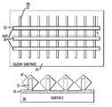
- boron-doped SiGeis employed in one or more embodiments for growth of both the merged epitaxy shown in FIG. 4 and the diamond-shaped volumes 42 on the sidewalls of the crystalline silicon fins 22 shown in FIG. 6 .
- phosphorus-doped SiGeis employed in one or more embodiments for growth of the merged epitaxy shown in FIG. 4 while the un-merged diamond-shaped volumes are formed with phosphorus-doped silicon (Si:P).
Landscapes
- Insulated Gate Type Field-Effect Transistor (AREA)
Abstract
Description
- Uniform doping of fins;
- Effective doping of fin bottom portions;
- Avoidance of crystal defectivity;
- Avoidance of enhanced lateral growth on isolated fin or outer fins in fin array (accidental merge of n-fin and p-fin in eDRAM regions)
- Multiple fabrication steps using a single tool;
Claims (22)
Priority Applications (1)
| Application Number | Priority Date | Filing Date | Title |
|---|---|---|---|
| US13/828,276US8796093B1 (en) | 2013-03-14 | 2013-03-14 | Doping of FinFET structures |
Applications Claiming Priority (1)
| Application Number | Priority Date | Filing Date | Title |
|---|---|---|---|
| US13/828,276US8796093B1 (en) | 2013-03-14 | 2013-03-14 | Doping of FinFET structures |
Publications (1)
| Publication Number | Publication Date |
|---|---|
| US8796093B1true US8796093B1 (en) | 2014-08-05 |
Family
ID=51229008
Family Applications (1)
| Application Number | Title | Priority Date | Filing Date |
|---|---|---|---|
| US13/828,276ActiveUS8796093B1 (en) | 2013-03-14 | 2013-03-14 | Doping of FinFET structures |
Country Status (1)
| Country | Link |
|---|---|
| US (1) | US8796093B1 (en) |
Cited By (35)
| Publication number | Priority date | Publication date | Assignee | Title |
|---|---|---|---|---|
| US20130187228A1 (en)* | 2012-01-19 | 2013-07-25 | Globalfoundries Inc. | FinFET Semiconductor Devices with Improved Source/Drain Resistance and Methods of Making Same |
| US20140308782A1 (en)* | 2013-04-15 | 2014-10-16 | International Business Machines Corporation | Self-limiting selective epitaxy process for preventing merger of semiconductor fins |
| US20150041908A1 (en)* | 2013-08-07 | 2015-02-12 | International Business Machines Corporation | METHOD OF MANUFACTURING A FinFET DEVICE USING A SACRIFICIAL EPITAXY REGION FOR IMPROVED FIN MERGE AND FinFET DEVICE FORMED BY SAME |
| US20150084101A1 (en)* | 2013-09-20 | 2015-03-26 | International Business Machines Corporation | Multi-fin finfets with merged-fin source/drains and replacement gates |
| US20150145067A1 (en)* | 2013-11-28 | 2015-05-28 | United Microelectronics Corp. | Fin structure |
| US20150214369A1 (en)* | 2014-01-27 | 2015-07-30 | Globalfoundries Inc. | Methods of forming epitaxial semiconductor material on source/drain regions of a finfet semiconductor device and the resulting devices |
| US20150357434A1 (en)* | 2014-01-30 | 2015-12-10 | International Business Machines Corporation | Replacement metal gate including dielectric gate material |
| US9299706B1 (en)* | 2014-09-25 | 2016-03-29 | International Business Machines Corporation | Single source/drain epitaxy for co-integrating nFET semiconductor fins and pFET semiconductor fins |
| US9368512B1 (en) | 2015-06-03 | 2016-06-14 | International Business Machines Corporation | Double diamond shaped unmerged epitaxy for tall fins in tight pitch |
| KR20160106819A (en)* | 2015-03-02 | 2016-09-13 | 삼성전자주식회사 | Semiconductor devices and methods of manufacturing semiconductor devices |
| KR20160119889A (en)* | 2015-04-06 | 2016-10-17 | 삼성전자주식회사 | Semiconductor devices and methods of manufacturing semiconductor devices |
| US9472470B2 (en) | 2014-12-09 | 2016-10-18 | GlobalFoundries, Inc. | Methods of forming FinFET with wide unmerged source drain EPI |
| US9564369B1 (en) | 2015-10-21 | 2017-02-07 | Samsung Electronics Co., Ltd. | Methods of manufacturing semiconductor devices including device isolation processes |
| US9595611B2 (en) | 2013-08-01 | 2017-03-14 | Samsung Electronics Co., Ltd. | FinFET with a single contact to multiple fins bridged together to form a source/drain region of the transistor |
| US20170098585A1 (en)* | 2015-10-02 | 2017-04-06 | Globalfoundries Inc. | Source/drain epitaxial electrical monitor |
| US9620416B1 (en) | 2015-11-18 | 2017-04-11 | International Business Machines Corporation | Fin field effect transistor structure and method to form defect free merged source and drain epitaxy for low external resistance |
| US9653605B2 (en) | 2014-10-17 | 2017-05-16 | Taiwan Semiconductor Manufacturing Company, Ltd. | Fin field effect transistor (FinFET) device and method for forming the same |
| US9728601B2 (en) | 2015-03-30 | 2017-08-08 | Samsung Electronics Co., Ltd. | Semiconductor devices including active fins and methods of manufacturing the same |
| US9793381B2 (en) | 2015-06-04 | 2017-10-17 | Samsung Electronics Co., Ltd. | Method for manufacturing a semiconductor device |
| CN107464846A (en)* | 2016-06-02 | 2017-12-12 | 三星电子株式会社 | Field-effect transistor and semiconductor structure |
| US9881919B2 (en)* | 2016-03-03 | 2018-01-30 | International Business Machines Corporation | Well and punch through stopper formation using conformal doping |
| US20180076306A1 (en)* | 2015-03-31 | 2018-03-15 | Stmicroelectronics, Inc. | Dual width finfet |
| US9954107B2 (en)* | 2015-05-05 | 2018-04-24 | International Business Machines Corporation | Strained FinFET source drain isolation |
| US10121791B2 (en)* | 2017-01-24 | 2018-11-06 | Samsung Electronics Co., Ltd. | Multi-gate transistor |
| US10164030B2 (en) | 2014-09-23 | 2018-12-25 | Samsung Electronics Co., Ltd. | Semiconductor device and method of fabricating the same |
| US20190035913A1 (en)* | 2017-07-25 | 2019-01-31 | International Business Machines Corporation | Nanosheet transitor with optimized junction and cladding defectivity control |
| US10249542B2 (en) | 2017-01-12 | 2019-04-02 | International Business Machines Corporation | Self-aligned doping in source/drain regions for low contact resistance |
| US10262904B2 (en) | 2017-03-22 | 2019-04-16 | International Business Machines Corporation | Vertical transistor top epitaxy source/drain and contact structure |
| US10319841B2 (en) | 2017-08-22 | 2019-06-11 | Samsung Electronics Co., Ltd. | Integrated circuit device including asymmetrical fin field-effect transistor |
| US10354930B2 (en) | 2016-04-21 | 2019-07-16 | International Business Machines Corporation | S/D contact resistance measurement on FinFETs |
| CN110634951A (en)* | 2018-06-25 | 2019-12-31 | 中芯国际集成电路制造(上海)有限公司 | Semiconductor device and method of forming the same |
| US20200027793A1 (en)* | 2016-03-04 | 2020-01-23 | Taiwan Semiconductor Manufacturing Co., Ltd. | Semiconductor device and manufacturing method thereof |
| US10964695B2 (en)* | 2018-10-30 | 2021-03-30 | Taiwan Semiconductor Manufacturing Co., Ltd. | Semiconductor structure |
| TWI773938B (en)* | 2018-11-29 | 2022-08-11 | 台灣積體電路製造股份有限公司 | Integrated circuit device and method forming same |
| US12439657B2 (en) | 2018-11-29 | 2025-10-07 | Taiwan Semiconductor Manufacturing Company, Ltd. | Confined source/drain epitaxy regions and method forming same |
Citations (12)
| Publication number | Priority date | Publication date | Assignee | Title |
|---|---|---|---|---|
| US6413802B1 (en) | 2000-10-23 | 2002-07-02 | The Regents Of The University Of California | Finfet transistor structures having a double gate channel extending vertically from a substrate and methods of manufacture |
| US20070026615A1 (en)* | 2005-07-27 | 2007-02-01 | Sinan Goktepeli | Method of forming a FINFET structure |
| US20070241399A1 (en)* | 2006-02-15 | 2007-10-18 | Toshifumi Irisawa | Semiconductor device and method of fabricating the same |
| US20090020819A1 (en)* | 2007-07-16 | 2009-01-22 | Anderson Brent A | Fin-type field effect transistor structure with merged source/drain silicide and method of forming the structure |
| US20090026505A1 (en)* | 2007-07-27 | 2009-01-29 | Kabushiki Kaisha Toshiba | Semiconductor device and method of fabricating the same |
| US20100244103A1 (en)* | 2009-03-30 | 2010-09-30 | International Business Machines Corporation | Structure and method of fabricating finfet |
| US20110133285A1 (en)* | 2009-12-07 | 2011-06-09 | Taiwan Semiconductor Manufacturing Company, Ltd. | SRAM Structure with FinFETs Having Multiple Fins |
| US20110210404A1 (en)* | 2010-02-26 | 2011-09-01 | Taiwan Seminconductor Manufacturing Company, Ltd. | Epitaxy Profile Engineering for FinFETs |
| US20110291188A1 (en)* | 2010-05-25 | 2011-12-01 | International Business Machines Corporation | Strained finfet |
| US20110309333A1 (en)* | 2010-06-21 | 2011-12-22 | International Business Machines Corporation | Semiconductor devices fabricated by doped material layer as dopant source |
| US8169024B2 (en) | 2009-08-18 | 2012-05-01 | International Business Machines Corporation | Method of forming extremely thin semiconductor on insulator (ETSOI) device without ion implantation |
| US20130307076A1 (en)* | 2012-05-16 | 2013-11-21 | International Business Machines Corporation | Method and structure for forming fin resistors |
- 2013
- 2013-03-14USUS13/828,276patent/US8796093B1/enactiveActive
Patent Citations (12)
| Publication number | Priority date | Publication date | Assignee | Title |
|---|---|---|---|---|
| US6413802B1 (en) | 2000-10-23 | 2002-07-02 | The Regents Of The University Of California | Finfet transistor structures having a double gate channel extending vertically from a substrate and methods of manufacture |
| US20070026615A1 (en)* | 2005-07-27 | 2007-02-01 | Sinan Goktepeli | Method of forming a FINFET structure |
| US20070241399A1 (en)* | 2006-02-15 | 2007-10-18 | Toshifumi Irisawa | Semiconductor device and method of fabricating the same |
| US20090020819A1 (en)* | 2007-07-16 | 2009-01-22 | Anderson Brent A | Fin-type field effect transistor structure with merged source/drain silicide and method of forming the structure |
| US20090026505A1 (en)* | 2007-07-27 | 2009-01-29 | Kabushiki Kaisha Toshiba | Semiconductor device and method of fabricating the same |
| US20100244103A1 (en)* | 2009-03-30 | 2010-09-30 | International Business Machines Corporation | Structure and method of fabricating finfet |
| US8169024B2 (en) | 2009-08-18 | 2012-05-01 | International Business Machines Corporation | Method of forming extremely thin semiconductor on insulator (ETSOI) device without ion implantation |
| US20110133285A1 (en)* | 2009-12-07 | 2011-06-09 | Taiwan Semiconductor Manufacturing Company, Ltd. | SRAM Structure with FinFETs Having Multiple Fins |
| US20110210404A1 (en)* | 2010-02-26 | 2011-09-01 | Taiwan Seminconductor Manufacturing Company, Ltd. | Epitaxy Profile Engineering for FinFETs |
| US20110291188A1 (en)* | 2010-05-25 | 2011-12-01 | International Business Machines Corporation | Strained finfet |
| US20110309333A1 (en)* | 2010-06-21 | 2011-12-22 | International Business Machines Corporation | Semiconductor devices fabricated by doped material layer as dopant source |
| US20130307076A1 (en)* | 2012-05-16 | 2013-11-21 | International Business Machines Corporation | Method and structure for forming fin resistors |
Cited By (71)
| Publication number | Priority date | Publication date | Assignee | Title |
|---|---|---|---|---|
| US9147765B2 (en)* | 2012-01-19 | 2015-09-29 | Globalfoundries Inc. | FinFET semiconductor devices with improved source/drain resistance and methods of making same |
| US20130187228A1 (en)* | 2012-01-19 | 2013-07-25 | Globalfoundries Inc. | FinFET Semiconductor Devices with Improved Source/Drain Resistance and Methods of Making Same |
| US20140308782A1 (en)* | 2013-04-15 | 2014-10-16 | International Business Machines Corporation | Self-limiting selective epitaxy process for preventing merger of semiconductor fins |
| US9752251B2 (en)* | 2013-04-15 | 2017-09-05 | International Business Machines Corporation | Self-limiting selective epitaxy process for preventing merger of semiconductor fins |
| US10727348B2 (en) | 2013-08-01 | 2020-07-28 | Samsung Electronics Co., Ltd. | Semiconductor device with adjacent source/drain regions connected by a semiconductor bridge, and method for fabricating the same |
| US10388791B2 (en) | 2013-08-01 | 2019-08-20 | Samsung Electronics Co., Ltd. | Semiconductor device with adjacent source/drain regions connected by a semiconductor bridge, and method for fabricating the same |
| US9595611B2 (en) | 2013-08-01 | 2017-03-14 | Samsung Electronics Co., Ltd. | FinFET with a single contact to multiple fins bridged together to form a source/drain region of the transistor |
| US9054218B2 (en)* | 2013-08-07 | 2015-06-09 | International Business Machines Corporation | Method of manufacturing a FinFET device using a sacrificial epitaxy region for improved fin merge and FinFET device formed by same |
| US20150228671A1 (en)* | 2013-08-07 | 2015-08-13 | International Business Machines Corporation | METHOD OF MANUFACTURING A FinFET DEVICE USING A SACRIFICIAL EPITAXY REGION FOR IMPROVED FIN MERGE AND FinFET DEVICE FORMED BY SAME |
| US9362310B2 (en)* | 2013-08-07 | 2016-06-07 | Globalfoundries Inc. | Method of manufacturing a FinFET device using a sacrificial epitaxy region for improved fin merge and FinFET device formed by same |
| US20150041908A1 (en)* | 2013-08-07 | 2015-02-12 | International Business Machines Corporation | METHOD OF MANUFACTURING A FinFET DEVICE USING A SACRIFICIAL EPITAXY REGION FOR IMPROVED FIN MERGE AND FinFET DEVICE FORMED BY SAME |
| US9048262B2 (en)* | 2013-09-20 | 2015-06-02 | International Business Machines Corporation | Multi-fin finFETs with merged-fin source/drains and replacement gates |
| US20150084101A1 (en)* | 2013-09-20 | 2015-03-26 | International Business Machines Corporation | Multi-fin finfets with merged-fin source/drains and replacement gates |
| US20150145067A1 (en)* | 2013-11-28 | 2015-05-28 | United Microelectronics Corp. | Fin structure |
| US20150214369A1 (en)* | 2014-01-27 | 2015-07-30 | Globalfoundries Inc. | Methods of forming epitaxial semiconductor material on source/drain regions of a finfet semiconductor device and the resulting devices |
| US20150357434A1 (en)* | 2014-01-30 | 2015-12-10 | International Business Machines Corporation | Replacement metal gate including dielectric gate material |
| US9653573B2 (en)* | 2014-01-30 | 2017-05-16 | International Business Machines Corporation | Replacement metal gate including dielectric gate material |
| US10164030B2 (en) | 2014-09-23 | 2018-12-25 | Samsung Electronics Co., Ltd. | Semiconductor device and method of fabricating the same |
| US9299706B1 (en)* | 2014-09-25 | 2016-03-29 | International Business Machines Corporation | Single source/drain epitaxy for co-integrating nFET semiconductor fins and pFET semiconductor fins |
| US9659938B2 (en) | 2014-09-25 | 2017-05-23 | International Business Machines Corporation | Single source/drain epitaxy for co-integrating nFET semiconductor fins and pFET semiconductor fins |
| US10304831B2 (en) | 2014-09-25 | 2019-05-28 | International Business Machines Corporation | Single source/drain epitaxy for co-integrating nFET semiconductor fins and pFET semiconductor fins |
| US10546956B2 (en) | 2014-10-17 | 2020-01-28 | Taiwan Semiconductor Manufacturing Co., Ltd. | Fin field effect transistor (FinFET) device and method for forming the same |
| US9653605B2 (en) | 2014-10-17 | 2017-05-16 | Taiwan Semiconductor Manufacturing Company, Ltd. | Fin field effect transistor (FinFET) device and method for forming the same |
| US11721762B2 (en) | 2014-10-17 | 2023-08-08 | Taiwan Semiconductor Manufacturing Co., Ltd. | Fin field effect transistor (FinFET) device and method for forming the same |
| US10164109B2 (en) | 2014-10-17 | 2018-12-25 | Taiwan Semiconductor Manufacturing Co., Ltd. | Fin field effect transistor (FinFET) device and method for forming the same |
| US10164108B2 (en)* | 2014-10-17 | 2018-12-25 | Taiwan Semiconductor Manufacturing Co., Ltd. | Fin field effect transistor (FinFET) device and method for forming the same |
| US11158744B2 (en) | 2014-10-17 | 2021-10-26 | Taiwan Semiconductor Manufacturing Co., Ltd. | Fin field effect transistor (FinFET) device and method for forming the same |
| US10964819B2 (en) | 2014-10-17 | 2021-03-30 | Taiwan Semiconductor Manufacturing Co., Ltd. | Fin field effect transistor (FinFET) device and method for forming the same |
| US10686077B2 (en) | 2014-10-17 | 2020-06-16 | Taiwan Semiconductor Manufacturing Co., Ltd. | Fin field effect transistor (FinFET) device and method for forming the same |
| US10840378B2 (en) | 2014-10-17 | 2020-11-17 | Taiwan Semiconductor Manufacturing Co., Ltd. | Fin field effect transistor (FinFET) device and method for forming the same |
| US9472470B2 (en) | 2014-12-09 | 2016-10-18 | GlobalFoundries, Inc. | Methods of forming FinFET with wide unmerged source drain EPI |
| US11211490B2 (en) | 2015-03-02 | 2021-12-28 | Samsung Electronics Co., Ltd. | FinFETs having step sided contact plugs and methods of manufacturing the same |
| US11764299B2 (en) | 2015-03-02 | 2023-09-19 | Samsung Electronics Co., Ltd. | FinFETs having step sided contact plugs and methods of manufacturing the same |
| KR20160106819A (en)* | 2015-03-02 | 2016-09-13 | 삼성전자주식회사 | Semiconductor devices and methods of manufacturing semiconductor devices |
| US12206022B2 (en) | 2015-03-02 | 2025-01-21 | Samsung Electronics Co., Ltd. | FINFETS having step sided contact plugs and methods of manufacturing the same |
| US9728601B2 (en) | 2015-03-30 | 2017-08-08 | Samsung Electronics Co., Ltd. | Semiconductor devices including active fins and methods of manufacturing the same |
| US10242917B2 (en) | 2015-03-30 | 2019-03-26 | Samsung Electronics Co., Ltd. | Semiconductor devices including active fins and methods of manufacturing the same |
| US20180076306A1 (en)* | 2015-03-31 | 2018-03-15 | Stmicroelectronics, Inc. | Dual width finfet |
| US10886386B2 (en)* | 2015-03-31 | 2021-01-05 | Stmicroelectronics, Inc. | Dual width FinFET |
| US9859387B2 (en) | 2015-04-06 | 2018-01-02 | Samsung Electronics Co., Ltd. | Semiconductor device having contact plugs |
| KR20160119889A (en)* | 2015-04-06 | 2016-10-17 | 삼성전자주식회사 | Semiconductor devices and methods of manufacturing semiconductor devices |
| US10586867B2 (en) | 2015-05-05 | 2020-03-10 | International Business Machines Corporation | Strained FinFET source drain isloation |
| US9954107B2 (en)* | 2015-05-05 | 2018-04-24 | International Business Machines Corporation | Strained FinFET source drain isolation |
| US9368512B1 (en) | 2015-06-03 | 2016-06-14 | International Business Machines Corporation | Double diamond shaped unmerged epitaxy for tall fins in tight pitch |
| US9793381B2 (en) | 2015-06-04 | 2017-10-17 | Samsung Electronics Co., Ltd. | Method for manufacturing a semiconductor device |
| US20170098585A1 (en)* | 2015-10-02 | 2017-04-06 | Globalfoundries Inc. | Source/drain epitaxial electrical monitor |
| US9972550B2 (en)* | 2015-10-02 | 2018-05-15 | Globalfoundries Inc. | Source/drain epitaxial electrical monitor |
| US9564369B1 (en) | 2015-10-21 | 2017-02-07 | Samsung Electronics Co., Ltd. | Methods of manufacturing semiconductor devices including device isolation processes |
| US9985114B2 (en) | 2015-11-18 | 2018-05-29 | International Business Machines Corporation | Fin field effect transistor structure and method to form defect free merged source and drain epitaxy for low external resistance |
| US9620416B1 (en) | 2015-11-18 | 2017-04-11 | International Business Machines Corporation | Fin field effect transistor structure and method to form defect free merged source and drain epitaxy for low external resistance |
| US9881919B2 (en)* | 2016-03-03 | 2018-01-30 | International Business Machines Corporation | Well and punch through stopper formation using conformal doping |
| US20200027793A1 (en)* | 2016-03-04 | 2020-01-23 | Taiwan Semiconductor Manufacturing Co., Ltd. | Semiconductor device and manufacturing method thereof |
| US10354930B2 (en) | 2016-04-21 | 2019-07-16 | International Business Machines Corporation | S/D contact resistance measurement on FinFETs |
| US11843051B2 (en) | 2016-06-02 | 2023-12-12 | Samsung Electronics Co., Ltd. | Field effect transistor including multiple aspect trapping ratio structures |
| CN107464846A (en)* | 2016-06-02 | 2017-12-12 | 三星电子株式会社 | Field-effect transistor and semiconductor structure |
| CN107464846B (en)* | 2016-06-02 | 2022-03-01 | 三星电子株式会社 | Field effect transistor and semiconductor structure |
| US11411111B2 (en) | 2016-06-02 | 2022-08-09 | Samsung Electronics Co., Ltd. | Field effect transistor including multiple aspect trapping ratio structures |
| US10249542B2 (en) | 2017-01-12 | 2019-04-02 | International Business Machines Corporation | Self-aligned doping in source/drain regions for low contact resistance |
| US10121791B2 (en)* | 2017-01-24 | 2018-11-06 | Samsung Electronics Co., Ltd. | Multi-gate transistor |
| US10262904B2 (en) | 2017-03-22 | 2019-04-16 | International Business Machines Corporation | Vertical transistor top epitaxy source/drain and contact structure |
| US10269652B2 (en) | 2017-03-22 | 2019-04-23 | International Business Machines Corporation | Vertical transistor top epitaxy source/drain and contact structure |
| US20190035913A1 (en)* | 2017-07-25 | 2019-01-31 | International Business Machines Corporation | Nanosheet transitor with optimized junction and cladding defectivity control |
| US10319841B2 (en) | 2017-08-22 | 2019-06-11 | Samsung Electronics Co., Ltd. | Integrated circuit device including asymmetrical fin field-effect transistor |
| US10573729B2 (en) | 2017-08-22 | 2020-02-25 | Samsung Electronics Co., Ltd. | Integrated circuit device including asymmetrical fin field-effect transistor |
| CN110634951B (en)* | 2018-06-25 | 2022-12-16 | 中芯国际集成电路制造(上海)有限公司 | Semiconductor device and method of forming the same |
| CN110634951A (en)* | 2018-06-25 | 2019-12-31 | 中芯国际集成电路制造(上海)有限公司 | Semiconductor device and method of forming the same |
| US11587926B2 (en) | 2018-10-30 | 2023-02-21 | Taiwan Semiconductor Manufacturing Company, Ltd. | Semiconductor structure |
| US10964695B2 (en)* | 2018-10-30 | 2021-03-30 | Taiwan Semiconductor Manufacturing Co., Ltd. | Semiconductor structure |
| TWI773938B (en)* | 2018-11-29 | 2022-08-11 | 台灣積體電路製造股份有限公司 | Integrated circuit device and method forming same |
| US11948971B2 (en) | 2018-11-29 | 2024-04-02 | Taiwan Semiconductor Manufacturing Company, Ltd. | Confined source/drain epitaxy regions and method forming same |
| US12439657B2 (en) | 2018-11-29 | 2025-10-07 | Taiwan Semiconductor Manufacturing Company, Ltd. | Confined source/drain epitaxy regions and method forming same |
Similar Documents
| Publication | Publication Date | Title |
|---|---|---|
| US8796093B1 (en) | Doping of FinFET structures | |
| US9514995B1 (en) | Implant-free punch through doping layer formation for bulk FinFET structures | |
| US9589848B2 (en) | FinFET structures having silicon germanium and silicon channels | |
| US8993399B2 (en) | FinFET structures having silicon germanium and silicon fins | |
| US9837415B2 (en) | FinFET structures having silicon germanium and silicon fins with suppressed dopant diffusion | |
| US10192888B2 (en) | Metallized junction FinFET structures | |
| US9455331B1 (en) | Method and structure of forming controllable unmerged epitaxial material | |
| US9437496B1 (en) | Merged source drain epitaxy | |
| US10002945B2 (en) | Composite spacer enabling uniform doping in recessed fin devices | |
| CN103137686B (en) | Semiconductor device and manufacture method thereof | |
| US10388571B2 (en) | Fin type field effect transistors with different pitches and substantially uniform fin reveal | |
| US9893181B1 (en) | Uniform gate length in vertical field effect transistors | |
| US9093275B2 (en) | Multi-height multi-composition semiconductor fins | |
| US9659779B2 (en) | Method and structure for enabling high aspect ratio sacrificial gates | |
| US20170025509A1 (en) | Strained silicon germanium fin with controlled junction for finfet devices | |
| US9449885B1 (en) | High germanium content FinFET devices having the same contact material for nFET and pFET devices | |
| CN106486372B (en) | Semiconductor device and method of making the same | |
| US10068920B2 (en) | Silicon germanium fins on insulator formed by lateral recrystallization | |
| US9536989B1 (en) | Field-effect transistors with source/drain regions of reduced topography | |
| US9159632B2 (en) | Fabrication method of semiconductor apparatus | |
| CN111627815B (en) | Methods for forming non-planar field effect transistors |
Legal Events
| Date | Code | Title | Description |
|---|---|---|---|
| AS | Assignment | Owner name:INTERNATIONAL BUSINESS MACHINES CORPORATION, NEW Y Free format text:ASSIGNMENT OF ASSIGNORS INTEREST;ASSIGNORS:CHENG, KANGGUO;DORIS, BRUCE B.;KHAKIFIROOZ, ALI;AND OTHERS;SIGNING DATES FROM 20130311 TO 20130312;REEL/FRAME:030002/0254 | |
| STCF | Information on status: patent grant | Free format text:PATENTED CASE | |
| AS | Assignment | Owner name:GLOBALFOUNDRIES U.S. 2 LLC, NEW YORK Free format text:ASSIGNMENT OF ASSIGNORS INTEREST;ASSIGNOR:INTERNATIONAL BUSINESS MACHINES CORPORATION;REEL/FRAME:036550/0001 Effective date:20150629 | |
| AS | Assignment | Owner name:GLOBALFOUNDRIES INC., CAYMAN ISLANDS Free format text:ASSIGNMENT OF ASSIGNORS INTEREST;ASSIGNORS:GLOBALFOUNDRIES U.S. 2 LLC;GLOBALFOUNDRIES U.S. INC.;REEL/FRAME:036779/0001 Effective date:20150910 | |
| MAFP | Maintenance fee payment | Free format text:PAYMENT OF MAINTENANCE FEE, 4TH YEAR, LARGE ENTITY (ORIGINAL EVENT CODE: M1551) Year of fee payment:4 | |
| AS | Assignment | Owner name:WILMINGTON TRUST, NATIONAL ASSOCIATION, DELAWARE Free format text:SECURITY AGREEMENT;ASSIGNOR:GLOBALFOUNDRIES INC.;REEL/FRAME:049490/0001 Effective date:20181127 | |
| AS | Assignment | Owner name:GLOBALFOUNDRIES U.S. INC., CALIFORNIA Free format text:ASSIGNMENT OF ASSIGNORS INTEREST;ASSIGNOR:GLOBALFOUNDRIES INC.;REEL/FRAME:054633/0001 Effective date:20201022 | |
| AS | Assignment | Owner name:GLOBALFOUNDRIES INC., CAYMAN ISLANDS Free format text:RELEASE BY SECURED PARTY;ASSIGNOR:WILMINGTON TRUST, NATIONAL ASSOCIATION;REEL/FRAME:054636/0001 Effective date:20201117 | |
| AS | Assignment | Owner name:GLOBALFOUNDRIES U.S. INC., NEW YORK Free format text:RELEASE BY SECURED PARTY;ASSIGNOR:WILMINGTON TRUST, NATIONAL ASSOCIATION;REEL/FRAME:056987/0001 Effective date:20201117 | |
| MAFP | Maintenance fee payment | Free format text:PAYMENT OF MAINTENANCE FEE, 8TH YEAR, LARGE ENTITY (ORIGINAL EVENT CODE: M1552); ENTITY STATUS OF PATENT OWNER: LARGE ENTITY Year of fee payment:8 |