US8795440B2 - Growth of non-polar M-plane III-nitride film using metalorganic chemical vapor deposition (MOCVD) - Google Patents
Growth of non-polar M-plane III-nitride film using metalorganic chemical vapor deposition (MOCVD)Download PDFInfo
- Publication number
- US8795440B2 US8795440B2US13/313,335US201113313335AUS8795440B2US 8795440 B2US8795440 B2US 8795440B2US 201113313335 AUS201113313335 AUS 201113313335AUS 8795440 B2US8795440 B2US 8795440B2
- Authority
- US
- United States
- Prior art keywords
- iii
- nitride crystal
- nitride
- polar
- plane
- Prior art date
- Legal status (The legal status is an assumption and is not a legal conclusion. Google has not performed a legal analysis and makes no representation as to the accuracy of the status listed.)
- Active
Links
Images


Classifications
- H—ELECTRICITY
- H01—ELECTRIC ELEMENTS
- H01L—SEMICONDUCTOR DEVICES NOT COVERED BY CLASS H10
- H01L21/00—Processes or apparatus adapted for the manufacture or treatment of semiconductor or solid state devices or of parts thereof
- H01L21/02—Manufacture or treatment of semiconductor devices or of parts thereof
- H01L21/04—Manufacture or treatment of semiconductor devices or of parts thereof the devices having potential barriers, e.g. a PN junction, depletion layer or carrier concentration layer
- H01L21/18—Manufacture or treatment of semiconductor devices or of parts thereof the devices having potential barriers, e.g. a PN junction, depletion layer or carrier concentration layer the devices having semiconductor bodies comprising elements of Group IV of the Periodic Table or AIIIBV compounds with or without impurities, e.g. doping materials
- H01L21/20—Deposition of semiconductor materials on a substrate, e.g. epitaxial growth solid phase epitaxy
- H—ELECTRICITY
- H01—ELECTRIC ELEMENTS
- H01L—SEMICONDUCTOR DEVICES NOT COVERED BY CLASS H10
- H01L21/00—Processes or apparatus adapted for the manufacture or treatment of semiconductor or solid state devices or of parts thereof
- H01L21/02—Manufacture or treatment of semiconductor devices or of parts thereof
- H01L21/02104—Forming layers
- H01L21/02365—Forming inorganic semiconducting materials on a substrate
- H01L21/02656—Special treatments
- H01L21/02658—Pretreatments
- C—CHEMISTRY; METALLURGY
- C30—CRYSTAL GROWTH
- C30B—SINGLE-CRYSTAL GROWTH; UNIDIRECTIONAL SOLIDIFICATION OF EUTECTIC MATERIAL OR UNIDIRECTIONAL DEMIXING OF EUTECTOID MATERIAL; REFINING BY ZONE-MELTING OF MATERIAL; PRODUCTION OF A HOMOGENEOUS POLYCRYSTALLINE MATERIAL WITH DEFINED STRUCTURE; SINGLE CRYSTALS OR HOMOGENEOUS POLYCRYSTALLINE MATERIAL WITH DEFINED STRUCTURE; AFTER-TREATMENT OF SINGLE CRYSTALS OR A HOMOGENEOUS POLYCRYSTALLINE MATERIAL WITH DEFINED STRUCTURE; APPARATUS THEREFOR
- C30B25/00—Single-crystal growth by chemical reaction of reactive gases, e.g. chemical vapour-deposition growth
- C30B25/02—Epitaxial-layer growth
- C30B25/18—Epitaxial-layer growth characterised by the substrate
- C—CHEMISTRY; METALLURGY
- C30—CRYSTAL GROWTH
- C30B—SINGLE-CRYSTAL GROWTH; UNIDIRECTIONAL SOLIDIFICATION OF EUTECTIC MATERIAL OR UNIDIRECTIONAL DEMIXING OF EUTECTOID MATERIAL; REFINING BY ZONE-MELTING OF MATERIAL; PRODUCTION OF A HOMOGENEOUS POLYCRYSTALLINE MATERIAL WITH DEFINED STRUCTURE; SINGLE CRYSTALS OR HOMOGENEOUS POLYCRYSTALLINE MATERIAL WITH DEFINED STRUCTURE; AFTER-TREATMENT OF SINGLE CRYSTALS OR A HOMOGENEOUS POLYCRYSTALLINE MATERIAL WITH DEFINED STRUCTURE; APPARATUS THEREFOR
- C30B29/00—Single crystals or homogeneous polycrystalline material with defined structure characterised by the material or by their shape
- C30B29/10—Inorganic compounds or compositions
- C30B29/40—AIIIBV compounds wherein A is B, Al, Ga, In or Tl and B is N, P, As, Sb or Bi
- C30B29/403—AIII-nitrides
- C30B29/406—Gallium nitride
- H—ELECTRICITY
- H01—ELECTRIC ELEMENTS
- H01L—SEMICONDUCTOR DEVICES NOT COVERED BY CLASS H10
- H01L21/00—Processes or apparatus adapted for the manufacture or treatment of semiconductor or solid state devices or of parts thereof
- H01L21/02—Manufacture or treatment of semiconductor devices or of parts thereof
- H01L21/02104—Forming layers
- H01L21/02365—Forming inorganic semiconducting materials on a substrate
- H01L21/02367—Substrates
- H01L21/0237—Materials
- H01L21/02373—Group 14 semiconducting materials
- H01L21/02378—Silicon carbide
- H—ELECTRICITY
- H01—ELECTRIC ELEMENTS
- H01L—SEMICONDUCTOR DEVICES NOT COVERED BY CLASS H10
- H01L21/00—Processes or apparatus adapted for the manufacture or treatment of semiconductor or solid state devices or of parts thereof
- H01L21/02—Manufacture or treatment of semiconductor devices or of parts thereof
- H01L21/02104—Forming layers
- H01L21/02365—Forming inorganic semiconducting materials on a substrate
- H01L21/02367—Substrates
- H01L21/0237—Materials
- H01L21/02387—Group 13/15 materials
- H01L21/02389—Nitrides
- H—ELECTRICITY
- H01—ELECTRIC ELEMENTS
- H01L—SEMICONDUCTOR DEVICES NOT COVERED BY CLASS H10
- H01L21/00—Processes or apparatus adapted for the manufacture or treatment of semiconductor or solid state devices or of parts thereof
- H01L21/02—Manufacture or treatment of semiconductor devices or of parts thereof
- H01L21/02104—Forming layers
- H01L21/02365—Forming inorganic semiconducting materials on a substrate
- H01L21/02367—Substrates
- H01L21/0237—Materials
- H01L21/0242—Crystalline insulating materials
- H—ELECTRICITY
- H01—ELECTRIC ELEMENTS
- H01L—SEMICONDUCTOR DEVICES NOT COVERED BY CLASS H10
- H01L21/00—Processes or apparatus adapted for the manufacture or treatment of semiconductor or solid state devices or of parts thereof
- H01L21/02—Manufacture or treatment of semiconductor devices or of parts thereof
- H01L21/02104—Forming layers
- H01L21/02365—Forming inorganic semiconducting materials on a substrate
- H01L21/02367—Substrates
- H01L21/02433—Crystal orientation
- H—ELECTRICITY
- H01—ELECTRIC ELEMENTS
- H01L—SEMICONDUCTOR DEVICES NOT COVERED BY CLASS H10
- H01L21/00—Processes or apparatus adapted for the manufacture or treatment of semiconductor or solid state devices or of parts thereof
- H01L21/02—Manufacture or treatment of semiconductor devices or of parts thereof
- H01L21/02104—Forming layers
- H01L21/02365—Forming inorganic semiconducting materials on a substrate
- H01L21/02436—Intermediate layers between substrates and deposited layers
- H01L21/02439—Materials
- H01L21/02455—Group 13/15 materials
- H01L21/02458—Nitrides
- H—ELECTRICITY
- H01—ELECTRIC ELEMENTS
- H01L—SEMICONDUCTOR DEVICES NOT COVERED BY CLASS H10
- H01L21/00—Processes or apparatus adapted for the manufacture or treatment of semiconductor or solid state devices or of parts thereof
- H01L21/02—Manufacture or treatment of semiconductor devices or of parts thereof
- H01L21/02104—Forming layers
- H01L21/02365—Forming inorganic semiconducting materials on a substrate
- H01L21/02436—Intermediate layers between substrates and deposited layers
- H01L21/02516—Crystal orientation
- H—ELECTRICITY
- H01—ELECTRIC ELEMENTS
- H01L—SEMICONDUCTOR DEVICES NOT COVERED BY CLASS H10
- H01L21/00—Processes or apparatus adapted for the manufacture or treatment of semiconductor or solid state devices or of parts thereof
- H01L21/02—Manufacture or treatment of semiconductor devices or of parts thereof
- H01L21/02104—Forming layers
- H01L21/02365—Forming inorganic semiconducting materials on a substrate
- H01L21/02518—Deposited layers
- H01L21/02521—Materials
- H01L21/02538—Group 13/15 materials
- H01L21/0254—Nitrides
- H—ELECTRICITY
- H01—ELECTRIC ELEMENTS
- H01L—SEMICONDUCTOR DEVICES NOT COVERED BY CLASS H10
- H01L21/00—Processes or apparatus adapted for the manufacture or treatment of semiconductor or solid state devices or of parts thereof
- H01L21/02—Manufacture or treatment of semiconductor devices or of parts thereof
- H01L21/02104—Forming layers
- H01L21/02365—Forming inorganic semiconducting materials on a substrate
- H01L21/02518—Deposited layers
- H01L21/02609—Crystal orientation
- H—ELECTRICITY
- H01—ELECTRIC ELEMENTS
- H01L—SEMICONDUCTOR DEVICES NOT COVERED BY CLASS H10
- H01L21/00—Processes or apparatus adapted for the manufacture or treatment of semiconductor or solid state devices or of parts thereof
- H01L21/02—Manufacture or treatment of semiconductor devices or of parts thereof
- H01L21/02104—Forming layers
- H01L21/02365—Forming inorganic semiconducting materials on a substrate
- H01L21/02612—Formation types
- H01L21/02617—Deposition types
- H01L21/0262—Reduction or decomposition of gaseous compounds, e.g. CVD
Definitions
- Denbaarsentitled “GROWTH OF PLANAR NON-POLAR ⁇ 1-1 0 0 ⁇ M-PLANE GALLIUM NITRIDE WITH METALORGANIC CHEMICAL VAPOR DEPOSITION (MOCVD)”;
- the present inventionrelates to the growth of non-polar m-plane III-nitride film using metalorganic chemical vapor deposition (MOCVD).
- MOCVDmetalorganic chemical vapor deposition
- Gallium nitride (GaN) and its ternary and quaternary compoundsare prime candidates for fabrication of visible and ultraviolet high-power and high-performance optoelectronic devices and electronic devices. These devices are typically grown epitaxially by growth techniques including molecular beam epitaxy (MBE), metalorganic chemical vapor deposition (MOCVD), or hydride vapor phase epitaxy (HVPE).
- MBEmolecular beam epitaxy
- MOCVDmetalorganic chemical vapor deposition
- HVPEhydride vapor phase epitaxy
- substrateis critical for achieving the desired GaN growth orientation.
- Some of the most widely used substrates for III-N growthinclude SiC, Al 2 O 3 , and LiAlO 2 .
- Various crystallographic orientations of these substratesare commercially available.
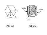
- FIGS. 1( a ) and 1 ( b )are schematics of crystallographic directions and planes of interest in hexagonal GaN. Specifically, these schematics show the different crystallographic growth directions and also the planes of interest in the hexagonal wurtzite GaN structure, wherein FIG. 1( a ) shows the crystallographic directions a 1 , a 2 , a 3 , c, ⁇ 10-10> and ⁇ 11-20>, and FIG. 1( b ) shows planes a (11-20), m (10-10) and r (10-12).
- the fill patterns of FIG. 1( b )are intended to illustrate the planes of interest, but do not represent the materials of the structure.
- Such polarization effectsdecrease the likelihood of electrons and holes recombining, causing the final device to perform poorly.
- One possible approach for eliminating piezoelectric polarization effects in GaN optoelectronic devicesis to grow the devices on non-polar planes of the crystal such as a- ⁇ 11-20 ⁇ and m- ⁇ 1-100 ⁇ planes family of GaN. Such planes contain equal numbers of Ga and N atoms and are charge-neutral.
- Planar ⁇ 1-100 ⁇ m-plane GaN growthhas been developed by HVPE and MBE methods. However, prior to the invention described herein, planar m-plane GaN growth had not been accomplished with MOCVD.
- the general purpose of the present inventionis to grow non-polar m-plane III-nitride film using MOCVD.
- the methodincludes performing a solvent clean and acid dip of an m-SiC substrate to remove oxide from the surface of the substrate ex situ prior to growth, in situ annealing of the substrate, growing a nucleation layer on the annealed substrate, and growing the non-polar m-plane III-nitride film on the nucleation layer using MOCVD.
- the present inventiontakes advantage of non-polar nature of the m-plane III-nitride film to eliminate polarization fields, and gives rise to flexibility in growth variables, such as temperature, pressure and precursor flows, utilizing the advantage of the m-plane III-nitride film's stability during growth.
- FIGS. 1( a ) and 1 ( b )are schematics of crystallographic directions and planes of interest in hexagonal GaN.
- FIGS. 2( a ) and 2 ( b )are schematics of band bending and electron hole separation as a result of polarization.
- FIG. 3provides a structural characterization of non-polar planar m-plane GaN on m-plane SiC, from top to bottom, wherein the crystal plane of interest is shown in a unit cell/
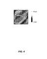
- FIG. 4is a 5 ⁇ m ⁇ 5 ⁇ m atomic force microscopy (AFM) surface image with a surface roughness value 2.54 nm.
- AFMatomic force microscopy
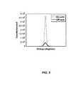
- FIG. 5is a graph that illustrates the xray diffraction rocking curves for on-axis and off-axis.
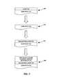
- FIG. 6is a flowchart that illustrates the processing steps for growing planar m-plane III-Nitrides using MOCVD according to the preferred embodiment of the present invention.
- FIG. 7further illustrates the results of the processing steps of FIG. 6 according to the preferred embodiment of the present invention.
- FIG. 3illustrates the non-polar m-plane GaN (1-100) crystal plane of interest in the unit cell.
- the most favorable conditionswere realized at low pressures, such as below 100 Torr, at temperatures in the range of 1100° C.-1160° C., and at VIII ratios below 700 with low NH 3 vapor pressure.
- a 5 ⁇ m ⁇ 5 ⁇ m atomic force microscopy (AFM) surface image of the resulting m-plane GaN materialis shown in FIG. 4 .
- the grainsare oriented along the ⁇ 11-20> direction and the surface roughness value (root mean square) is ⁇ 2.54 nm for a 5 ⁇ m ⁇ 5 ⁇ m scan.
- FIG. 5is a graph of omega (degrees) vs. counts/second showing the x-ray diffraction rocking curves on-axis and off-axis.
- on-axis (1-100) full width at half max (FWHM) valuesare measured as low as 0.22° and 1.2°, for a-mosaic and c-mosaic, respectively, and the off-axis (10-12) reflection has FWHM value of 0.38°.
- FIG. 6is a flowchart that illustrates the processing steps for growing a planar non polar ⁇ 1-100 ⁇ m-plane III-Nitride epitaxial film using MOCVD according to the preferred embodiment of the present invention, wherein the planar non polar m-plane III-Nitride epitaxial film may comprise a planar m-plane GaN epitaxial layer.
- FIG. 7further illustrates the results of each of the processing steps of FIG. 6 .
- Block 600represents a solvent clean and acid dip of a suitable substrate ( 700 ), for example, in a 1:10 diluted BHF:DI solution, to remove oxide ( 702 ) from the substrate ( 700 ) surface before loading the substrate ( 700 ) into a reactor for the growth step. (Although this step is recommended, its omission would not significantly alter the results.)
- the substrate ( 700 )may comprise an m-SiC or any substrate that is suitable for non-polar m-plane III-Nitride growth.
- Block 602represents in situ annealing of the substrate ( 700 ), for example, in hydrogen, prior to the growth step. (Although this step is recommended, its omission would not significantly alter the results.)
- Block 604represents growing a nucleation layer ( 704 ) on the substrate ( 700 ).
- the nucleation layer ( 704 )typically comprises an aluminum nitride (AlN) nucleation layer or interlayer, but may comprise any nucleation layer ( 704 ) that is appropriate for non-polar m-plane III-Nitride growth.
- the nucleation layer ( 704 )may be grown after the annealing step, and prior to the non polar m-plane III-Nitride growth.
- Block 606represents growing the non-polar m-plane III-Nitride epitaxial layer ( 706 ) using MOCVD.
- the non-polar m-plane III-Nitride epitaxial layer ( 706 )typically comprises a non-polar m-plane GaN epitaxial layer, but may comprise other non-polar m-plane III-Nitride epitaxial layers as well.
- the non-polar m-plane III-Nitride epitaxial layer ( 706 )may be grown on the nucleation layer ( 704 ), or on the substrate ( 700 ) itself.
- the end resultis a device, or a free standing wafer, or a substrate, or a template, having a planar epitaxial layer of the non-polar m-plane III-Nitride.
- non-polar m-GaN on m-SiC using an AlN interlayeralternative suitable substrates, on which the non-polar m-plane III-Nitride epitaxial film could be formed, include, but are not limited to, 6H or 4H m-plane SiC, freestanding m-GaN, LiGaO 2 and LiAlO 2 .
- the suitable substratePrior to growth, the suitable substrate can be treated in many different ways in-situ or ex-situ, or it may not be treated at all.
- the non-polar epitaxial filmcan be nucleated and grown over different nucleation layers, such as GaN or AlN grown at various conditions and methods, or over a bare substrate.
- the epitaxial filmcan be any non-polar m-plane III-Nitride material including, but not limited to, GaN, AlN, AlGaN and InGaN with various thicknesses.
- the growth parameters required for the growth of non-polar m-plane III-Nitride materialmay vary from reactor to reactor.
- the growth of m- ⁇ 1-100 ⁇ plane GaNhas been successfully demonstrated by HVPE and MBE.
- the present inventionis the first-ever successful demonstration of high-quality planar non-polar m- ⁇ 1-100 ⁇ plane GaN growth by MOCVD.
- planar m-plane GaNhas an advantage over growth of planar a- ⁇ 11-20 ⁇ GaN with MOCVD in terms of its stability with a large growth window. This was shown when growth variables such as temperature, pressure and precursor flows for AlN nucleation layer and GaN epitaxial film were changed.
Landscapes
- Engineering & Computer Science (AREA)
- Chemical & Material Sciences (AREA)
- Manufacturing & Machinery (AREA)
- General Physics & Mathematics (AREA)
- Physics & Mathematics (AREA)
- Computer Hardware Design (AREA)
- Microelectronics & Electronic Packaging (AREA)
- Power Engineering (AREA)
- Condensed Matter Physics & Semiconductors (AREA)
- Crystallography & Structural Chemistry (AREA)
- Materials Engineering (AREA)
- Metallurgy (AREA)
- Organic Chemistry (AREA)
- Inorganic Chemistry (AREA)
- Chemical Kinetics & Catalysis (AREA)
- General Chemical & Material Sciences (AREA)
- Crystals, And After-Treatments Of Crystals (AREA)
- Chemical Vapour Deposition (AREA)
Abstract
Description
This application is a continuation of and claims the benefit under 35 U.S.C. Section 120 of co-pending and commonly-assigned U.S. Utility patent application Ser. No. 11/870,115, filed on Oct. 10, 2007, by Bilge M. Imer, James S. Speck, Steven P. Denbaars, and Shuji Nakamura, entitled “GROWTH OF NON-POLAR M-PLANE III-NITRIDE FILM USING METALORGANIC CHEMICAL VAPOR DEPOSITION (MOCVD),” which application is a continuation of U.S. Utility patent application Ser. No. 11/444,083, filed on May 31, 2006, now U.S. Pat. No. 7,338,828, issued Mar. 4, 2008, by Bilge M. Imer, James S. Speck, Steven P. Denbaars, and Shuji Nakamura, entitled “GROWTH OF PLANAR NON-POLAR {1 -1 0 0} M-PLANE GALLIUM NITRIDE WITH METALORGANIC CHEMICAL VAPOR DEPOSITION (MOCVD),” which application claims the benefit under 35 U.S.C. Section 119(e) of U.S. Provisional Patent Application Ser. No. 60/685,908, filed on May 31, 2005, by Bilge M. Imer, James S. Speck and Steven P. Denbaars, entitled “GROWTH OF PLANAR NON-POLAR {1-1 0 0} M-PLANE GALLIUM NITRIDE WITH METALORGANIC CHEMICAL VAPOR DEPOSITION (MOCVD)”;
all of which applications are incorporated by reference herein.
This application is related to the following co-pending and commonly-assigned applications:
U.S. Utility patent application Ser. No. 11/444,084, filed on May 31, 2006, now U.S. Pat. No. 7,361,576, issued Apr. 22, 2008, by Bilge M. Imer, James S. Speck and Steven P. DenBaars, entitled “DEFECT REDUCTION OF NON-POLAR AND SEMI-POLAR III-NITRIDES WITH SIDEWALL LATERAL EPITAXIAL OVERGROWTH (SLEO),” which application claims the benefit under 35 U.S.C. Section 119(e) of U.S. Provisional Patent Application Ser. No. 60/685,952, filed on May 31, 2005 by Bilge M. Imer, James S. Speck and Steven P. DenBaars, entitled “DEFECT REDUCTION OF NON-POLAR GALLIUM NITRIDE WITH SINGLE-STEP SIDEWALL LATERAL EPITAXIAL OVERGROWTH”;
U.S. Utility patent application Ser. No. 10/537,385, filed Jun. 3, 2005, now U.S. Pat. No. 7,427,555, issued Sep. 23, 2008, by Benjamin A. Haskell, Paul T. Fini, Shigemasa Matsuda, Michael D. Craven, Steven P. DenBaars, James S. Speck, and Shuji Nakamura, entitled “GROWTH OF PLANAR, NON-POLAR A-PLANE GALLIUM NITRIDE BY HYDRIDE VAPOR PHASE EPITAXY,” which application claims priority to International Patent Application No. PCT/US03/21916, filed Jul. 15, 2003, by Benjamin A. Haskell, Paul T. Fini, Shigemasa Matsuda, Michael D. Craven, Steven P. DenBaars, James S. Speck, and Shuji Nakamura, entitled “GROWTH OF PLANAR, NON-POLAR A-PLANE GALLIUM NITRIDE BY HYDRIDE VAPOR PHASE EPITAXY,” which application claims priority to U.S. Provisional Patent Application Ser. No. 60/433,844, filed Dec. 16, 2002, by Benjamin A. Haskell, Paul T. Fini, Shigemasa Matsuda, Michael D. Craven, Steven P. DenBaars, James S. Speck, and Shuji Nakamura, entitled “TECHNIQUE FOR THE GROWTH OF PLANAR, NON-POLAR A-PLANE GALLIUM NITRIDE BY HYDRIDE VAPOR PHASE EPITAXY”; and
U.S. Utility patent application Ser. No. 10/413,691, filed Apr. 15, 2003, by Michael D. Craven and James S. Speck, entitled “NON-POLAR A-PLANE GALLIUM NITRIDE THIN FILMS GROWN BY METALORGANIC CHEMICAL VAPOR DEPOSITION,” which application claims priority to U.S. Provisional Patent Application Ser. No. 60/372,909, filed Apr. 15, 2002, by Michael D. Craven, Stacia Keller, Steven P. DenBaars, Tal Margalith, James S. Speck, Shuji Nakamura, and Umesh K. Mishra, entitled “NON-POLAR GALLIUM NITRIDE BASED THIN FILMS AND HETEROSTRUCTURE MATERIALS”;
all of which applications are incorporated by reference herein.
1. Field of the Invention
The present invention relates to the growth of non-polar m-plane III-nitride film using metalorganic chemical vapor deposition (MOCVD).
2. Description of the Related Art
Gallium nitride (GaN) and its ternary and quaternary compounds are prime candidates for fabrication of visible and ultraviolet high-power and high-performance optoelectronic devices and electronic devices. These devices are typically grown epitaxially by growth techniques including molecular beam epitaxy (MBE), metalorganic chemical vapor deposition (MOCVD), or hydride vapor phase epitaxy (HVPE).
The selection of substrate is critical for achieving the desired GaN growth orientation. Some of the most widely used substrates for III-N growth include SiC, Al2O3, and LiAlO2. Various crystallographic orientations of these substrates are commercially available.
It is relatively easy to grow planar c-plane GaN due to its large growth stability window. Therefore, nearly all GaN-based devices are grown parallel to the polar c-axis. However, as a result of c-plane growth, each material layer suffers from separation of electrons and holes to opposite faces of the layers. Furthermore, strain at the interfaces between adjacent layers gives rise to piezoelectric polarization, causing further charge separation.
Such polarization effects decrease the likelihood of electrons and holes recombining, causing the final device to perform poorly. One possible approach for eliminating piezoelectric polarization effects in GaN optoelectronic devices is to grow the devices on non-polar planes of the crystal such as a-{11-20} and m-{1-100} planes family of GaN. Such planes contain equal numbers of Ga and N atoms and are charge-neutral.
Planar {1-100} m-plane GaN growth has been developed by HVPE and MBE methods. However, prior to the invention described herein, planar m-plane GaN growth had not been accomplished with MOCVD.
The general purpose of the present invention is to grow non-polar m-plane III-nitride film using MOCVD. The method includes performing a solvent clean and acid dip of an m-SiC substrate to remove oxide from the surface of the substrate ex situ prior to growth, in situ annealing of the substrate, growing a nucleation layer on the annealed substrate, and growing the non-polar m-plane III-nitride film on the nucleation layer using MOCVD. The present invention takes advantage of non-polar nature of the m-plane III-nitride film to eliminate polarization fields, and gives rise to flexibility in growth variables, such as temperature, pressure and precursor flows, utilizing the advantage of the m-plane III-nitride film's stability during growth.
Referring now to the drawings in which like reference numbers represent corresponding parts throughout:
In the following description of the preferred embodiment, reference is made to the accompanying drawings that form a part hereof, and in which is shown by way of illustration a specific embodiment in which the invention may be practiced. It is to be understood that other embodiments may be utilized and structural changes may be made without departing from the scope of the present invention.
Overview
The growth of (Ga, In, Al, B)N materials in the polar [0001] c-direction causes lower performance in optical devices due to polarization fields causing charge separation along the primary conduction direction. Therefore, recent research has been conducted focusing on non-polar direction growth along a-[11-20] and m-[1-100] directions of these materials to eliminate such effects and so to improve the device performance significantly. While both a-plane and m-plane growth of GaN has been explored by HVPE and MBE, only non-polar a-{11-20} plane growth of GaN has been demonstrated by MOCVD. However, it has been found that the growth window for planar a-plane GaN is very small and this specific orientation is very sensitive to changes in growth variables such as pressure and precursor flows. This resulted in the exploration of a new non-polar orientation in GaN growth with MOCVD. However, for m-plane growth, substrate availability has been a problem due to high growth temperatures required in MOCVD. Commercially available substrates such as γ-LiAlO2have melting points lower than the temperature required for MOCVD growth. With the emergence of commercially obtainable m-SiC substrates, which are stable during MOCVD growth, the current invention was made possible. The present invention is the first ever successful growth of m-{1-100} plane GaN on m-SiC by MOCVD.
Technical Description
The m-plane SiC substrate is annealed in hydrogen prior to growth. An AlN layer is formed as a nucleation layer before GaN film growth. Finally, a GaN layer is grown by MOCVD.FIG. 3 illustrates the non-polar m-plane GaN (1-100) crystal plane of interest in the unit cell.
To accomplish the optimum quality m-plane GaN, VIII ratios of 400-5500 and 200-3000, growth pressures varying in between 50-760 Torr, and temperature series of 1100° C.-1275° C. and 1000° C.-1160° C. for AlN and GaN layers were tested, respectively. The m-plane, for both AlN and GaN, was stable over this wide range of temperatures, reactor pressures, and precursor flows.
The optimum AlN nucleation layers, leading to best quality GaN films, were realized at temperatures over 1175° C., at relatively low pressures, and VIII ratio of ˜3500 with the nucleation layer thickness below 150 nm.
For GaN layer epitaxy, the most favorable conditions were realized at low pressures, such as below 100 Torr, at temperatures in the range of 1100° C.-1160° C., and at VIII ratios below 700 with low NH3vapor pressure.
A 5 μm×5 μm atomic force microscopy (AFM) surface image of the resulting m-plane GaN material is shown inFIG. 4 . The grains are oriented along the <11-20> direction and the surface roughness value (root mean square) is ˜2.54 nm for a 5 μm×5 μm scan.
| TABLE 1 |
| Rocking curve FWHM values |
| On-Axis Values |
| a-mosaic | c-mosaic | Off-Axis |
| 0.22° | 1.2° | 0.38° |
Process Steps
Preferably, the end result is a device, or a free standing wafer, or a substrate, or a template, having a planar epitaxial layer of the non-polar m-plane III-Nitride.
Possible Modifications and Variations
Although the preferred embodiment describes the MOCVD growth of non-polar m-GaN on m-SiC using an AlN interlayer, alternative suitable substrates, on which the non-polar m-plane III-Nitride epitaxial film could be formed, include, but are not limited to, 6H or 4H m-plane SiC, freestanding m-GaN, LiGaO2and LiAlO2.
Prior to growth, the suitable substrate can be treated in many different ways in-situ or ex-situ, or it may not be treated at all.
The non-polar epitaxial film can be nucleated and grown over different nucleation layers, such as GaN or AlN grown at various conditions and methods, or over a bare substrate.
The epitaxial film can be any non-polar m-plane III-Nitride material including, but not limited to, GaN, AlN, AlGaN and InGaN with various thicknesses.
The growth parameters required for the growth of non-polar m-plane III-Nitride material may vary from reactor to reactor.
Finally, it is understood that processing steps may be omitted, added or rearranged as desired.
Such variations do not fundamentally alter the general practice of this invention.
Advantages and Improvements
The growth of m-{1-100} plane GaN has been successfully demonstrated by HVPE and MBE. However, the present invention is the first-ever successful demonstration of high-quality planar non-polar m-{1-100} plane GaN growth by MOCVD.
Growth of planar m-plane GaN has an advantage over growth of planar a-{11-20} GaN with MOCVD in terms of its stability with a large growth window. This was shown when growth variables such as temperature, pressure and precursor flows for AlN nucleation layer and GaN epitaxial film were changed.
To accomplish the optimum quality m-plane GaN, VIII ratios of 400-5500 and 200-3000, growth pressures varying in between 50-760 Torr, and temperature series of 1100° C.-1275° C. and 1000° C.-1160° C. for AlN and GaN layers were tested, respectively. Alterations in such conditions did not affect the crystal and surface quality significantly unlike the planar non-polar a-plane GaN films in which crystal and surface quality are extremely susceptible to change in growth conditions and constrained with small growth window.
The growth stability advantage combined with the non-polar nature of m-GaN brings new possibilities in III-Nitride non-polar device research.
The following reference is incorporated by reference herein:
1. “Molecular-beam epitaxy of GaN/AlxGa1-xN multiple quantum wells on R-plane (10-12) sapphire substrates,” H. M. Ng, Appl. Phys. Lett. 80, 4369 (2002)
This concludes the description of the preferred embodiment of the present invention. The foregoing description of one or more embodiments of the invention has been presented for the purposes of illustration and description. It is not intended to be exhaustive or to limit the invention to the precise form disclosed. Many modifications and variations are possible in light of the above teaching, such as additional adjustments to the process described herein, without fundamentally deviating from the essence of the present invention. It is intended that the scope of the invention be limited not by this detailed description, but rather by the claims appended hereto.
Claims (31)
1. A III-nitride crystal, comprising:
a top surface having an area of least 5 micrometers by 5 micrometers, wherein:
the top surface has a non-polar m-plane orientation, and
a surface roughness of the top surface, as grown, is not more than 2.54 nanometers at least for the area of 5 micrometers by 5 micrometers, and
the III-nitride crystal has a crystalline quality characterized by an off-axis rocking curve having an off-axis full width at half maximum (FWHM) of no more than 0.38°, as measured by X-ray diffraction.
2. The III-nitride crystal ofclaim 1 , wherein:
the III-nitride crystal has a crystalline quality characterized by an on-axis rocking curve having an on-axis (1-100) full width at half maximum (FWHM) of:
no more than 0.22°, for an a-mosaic of the III-nitride crystal, or
no more than 1.2°, for a c-mosaic of the III-nitride crystal or
no more than 0.22°, for an a-mosaic of the III-nitride crystal and no more than 1.2°, for a c-mosaic of the III-nitride crystal, and
the rocking curves are measured by X-ray diffraction.
3. The III-nitride crystal ofclaim 2 , wherein the off-axis is (10-12).
4. The III-nitride crystal ofclaim 1 , wherein the III-nitride crystal is a Gallium Nitride crystal.
5. The III-nitride crystal ofclaim 1 , wherein the III-nitride crystal comprises AlN, AlGaN or InGaN.
6. The III-nitride crystal ofclaim 1 , further comprising:
a nucleation or first nitride layer grown on a substrate; and
the III-nitride crystal grown on the nucleation layer or the first nitride layer.
7. The III-nitride crystal ofclaim 6 , wherein the nucleation layer or first nitride layer comprises aluminum nitride (AlN).
8. The III-nitride crystal ofclaim 1 , wherein the III-nitride crystal is a device, wafer, substrate, or template.
9. The III-nitride crystal ofclaim 8 , wherein the III-nitride crystal comprises Gallium Nitride.
10. The III-nitride crystal ofclaim 1 , wherein the III-nitride crystal is sufficiently thick to be free-standing.
11. The III-nitride crystal ofclaim 1 , further comprising a non-polar optoelectronic or electronic device grown on the top surface.
12. The III-nitride crystal ofclaim 1 , wherein the III-nitride crystal is grown on a Silicon Carbide substrate.
13. The III-nitride crystal ofclaim 1 , wherein the III-nitride crystal is grown on a Gallium Nitride substrate.
14. The III-nitride crystal ofclaim 1 , wherein the III-nitride crystal is grown on a LiGaO2or LiAlO2substrate.
15. The III-nitride crystal ofclaim 1 , wherein individual grains of the III-nitride crystal are not distinguishable based on height measurements of the surface.
16. The III-nitride crystal ofclaim 1 , wherein the surface results from predominantly stepped growth.
17. The crystal ofclaim 1 , wherein the top surface is a largest surface of the III-nitride crystal.
18. The III-nitride crystal ofclaim 1 , wherein the top surface is planar.
19. The III-nitride crystal ofclaim 1 , wherein the III-nitride crystal is an initial III-nitride crystal.
20. A device structure comprising the III-nitride crystal ofclaim 1 , wherein:
the III-nitride crystal is a non-polar m-plane film having a crystalline quality characterized by a rocking curve having a full width at half maximum (FWHM) of no more than 0.22° as measured by X-Ray diffraction, and
the top surface of the non-polar m-plane film is epitaxially grown.
21. The device structure ofclaim 20 , wherein the non-polar m-plane III-nitride film comprises different III-nitride layers.
22. A device structure, comprising:
a non-polar m-plane III-nitride crystal, wherein:
the non-polar m-plane III-nitride crystal is grown on a surface of a substrate,
a subsequent non-polar m-plane III-nitride layer is grown on a top surface of the non-polar m-plane III-nitride crystal,
the top surface includes an area with a root mean square surface roughness of not more than 2.54 nanometers at least for an area of 5 micrometers by 5 micrometers, and
the III-nitride crystal has a crystalline quality characterized by an off-axis rocking curve having an off-axis full width at half maximum (FWHM) of no more than 0.38°, as measured by X-ray diffraction.
23. A method for growing an III-nitride crystal, comprising:
growing a top surface of a III-nitride crystal using growth conditions, wherein:
the top surface has an area of least 5 micrometers by 5 micrometers,
the top surface has a non-polar m-plane orientation,
a surface roughness of the top surface, as grown, is not more than 2.54 nanometers
at least for the area of 5 micrometers by 5 micrometers,
the III-nitride crystal has a crystalline quality characterized by an off-axis rocking
curve having an off-axis full width at half maximum (FWHM) of no more than 0.38°, as measured by X-ray diffraction.
24. The method ofclaim 23 , wherein the growing is by Metal Organic Chemical Vapor Deposition using optimized growth conditions.
25. The method ofclaim 23 , wherein the III-nitride crystal is Gallium Nitride or Aluminum Nitride, and the growing is at:
a V/III ratio between 200-5500,
a growth pressure between 50-760 Torr, and
a growth temperature of at least 1000° C.
26. The method ofclaim 25 , further comprising:
growing an Aluminum Nitride (AlN) layer on the substrate at a temperature over 1175° C. and to a thickness below 150 nanometers; and
growing the III-nitride crystal on the AlN layer.
27. The method ofclaim 23 , wherein the III-nitride crystal is Gallium Nitride and the growing is at a growth pressure below 100 Torr.
28. The method ofclaim 27 , wherein the growing is at a V/III ratio below 700.
29. The method ofclaim 28 , wherein the growing is at a temperature in a range of 1100° C.-1160° C.
30. The method ofclaim 23 , further comprising:
growing a first nitride layer on a substrate at a temperature of at least 1000° C., and growing the non-polar m-plane III-Nitride layer on the first nitride layer, at the temperature of at least 1000° C.
31. The method ofclaim 30 , wherein the first III-nitride layer comprises aluminum nitride (AlN) or Gallium Nitride.
Priority Applications (1)
| Application Number | Priority Date | Filing Date | Title |
|---|---|---|---|
| US13/313,335US8795440B2 (en) | 2005-05-31 | 2011-12-07 | Growth of non-polar M-plane III-nitride film using metalorganic chemical vapor deposition (MOCVD) |
Applications Claiming Priority (4)
| Application Number | Priority Date | Filing Date | Title |
|---|---|---|---|
| US68590805P | 2005-05-31 | 2005-05-31 | |
| US11/444,083US7338828B2 (en) | 2005-05-31 | 2006-05-31 | Growth of planar non-polar {1 -1 0 0} m-plane gallium nitride with metalorganic chemical vapor deposition (MOCVD) |
| US11/870,115US8097481B2 (en) | 2005-05-31 | 2007-10-10 | Growth of non-polar M-plane III-nitride film using metalorganic chemical vapor deposition (MOCVD) |
| US13/313,335US8795440B2 (en) | 2005-05-31 | 2011-12-07 | Growth of non-polar M-plane III-nitride film using metalorganic chemical vapor deposition (MOCVD) |
Related Parent Applications (1)
| Application Number | Title | Priority Date | Filing Date |
|---|---|---|---|
| US11/870,115ContinuationUS8097481B2 (en) | 2004-06-03 | 2007-10-10 | Growth of non-polar M-plane III-nitride film using metalorganic chemical vapor deposition (MOCVD) |
Publications (2)
| Publication Number | Publication Date |
|---|---|
| US20120074429A1 US20120074429A1 (en) | 2012-03-29 |
| US8795440B2true US8795440B2 (en) | 2014-08-05 |
Family
ID=37482235
Family Applications (3)
| Application Number | Title | Priority Date | Filing Date |
|---|---|---|---|
| US11/444,083ActiveUS7338828B2 (en) | 2005-05-31 | 2006-05-31 | Growth of planar non-polar {1 -1 0 0} m-plane gallium nitride with metalorganic chemical vapor deposition (MOCVD) |
| US11/870,115Active2027-11-28US8097481B2 (en) | 2004-06-03 | 2007-10-10 | Growth of non-polar M-plane III-nitride film using metalorganic chemical vapor deposition (MOCVD) |
| US13/313,335ActiveUS8795440B2 (en) | 2005-05-31 | 2011-12-07 | Growth of non-polar M-plane III-nitride film using metalorganic chemical vapor deposition (MOCVD) |
Family Applications Before (2)
| Application Number | Title | Priority Date | Filing Date |
|---|---|---|---|
| US11/444,083ActiveUS7338828B2 (en) | 2005-05-31 | 2006-05-31 | Growth of planar non-polar {1 -1 0 0} m-plane gallium nitride with metalorganic chemical vapor deposition (MOCVD) |
| US11/870,115Active2027-11-28US8097481B2 (en) | 2004-06-03 | 2007-10-10 | Growth of non-polar M-plane III-nitride film using metalorganic chemical vapor deposition (MOCVD) |
Country Status (6)
| Country | Link |
|---|---|
| US (3) | US7338828B2 (en) |
| EP (1) | EP1897120A4 (en) |
| JP (2) | JP2008543087A (en) |
| KR (2) | KR101499203B1 (en) |
| TW (1) | TWI377602B (en) |
| WO (1) | WO2006130622A2 (en) |
Cited By (3)
| Publication number | Priority date | Publication date | Assignee | Title |
|---|---|---|---|---|
| US20130256743A1 (en)* | 2012-03-30 | 2013-10-03 | Toyoda Gosei Co., Ltd. | Production method for group iii nitride semiconductor and group iii nitride semiconductor |
| US20150008563A1 (en)* | 2006-11-17 | 2015-01-08 | Sumitomo Electric Industries, Ltd. | Composite of III-Nitride Crystal on Laterally Stacked Substrates |
| US11688601B2 (en) | 2020-11-30 | 2023-06-27 | International Business Machines Corporation | Obtaining a clean nitride surface by annealing |
Families Citing this family (162)
| Publication number | Priority date | Publication date | Assignee | Title |
|---|---|---|---|---|
| US9130119B2 (en)* | 2006-12-11 | 2015-09-08 | The Regents Of The University Of California | Non-polar and semi-polar light emitting devices |
| US7842527B2 (en)* | 2006-12-11 | 2010-11-30 | The Regents Of The University Of California | Metalorganic chemical vapor deposition (MOCVD) growth of high performance non-polar III-nitride optical devices |
| TWI377602B (en)* | 2005-05-31 | 2012-11-21 | Japan Science & Tech Agency | Growth of planar non-polar {1-100} m-plane gallium nitride with metalorganic chemical vapor deposition (mocvd) |
| JP2007277074A (en)* | 2006-01-10 | 2007-10-25 | Ngk Insulators Ltd | Manufacturing method of alminum nitride single crystal and aluminum nitride single crystal |
| GB2436398B (en)* | 2006-03-23 | 2011-08-24 | Univ Bath | Growth method using nanostructure compliant layers and HVPE for producing high quality compound semiconductor materials |
| EP2004882A2 (en)* | 2006-04-07 | 2008-12-24 | The Regents of the University of California | Growing large surface area gallium nitride crystals |
| TWI334164B (en)* | 2006-06-07 | 2010-12-01 | Ind Tech Res Inst | Method of manufacturing nitride semiconductor substrate and composite material substrate |
| US20080083431A1 (en)* | 2006-10-06 | 2008-04-10 | Mark Schwarze | Device and method for clearing debris from the front of a hood in a mechanized sweepers |
| US8458262B2 (en)* | 2006-12-22 | 2013-06-04 | At&T Mobility Ii Llc | Filtering spam messages across a communication network |
| GB0701069D0 (en)* | 2007-01-19 | 2007-02-28 | Univ Bath | Nanostructure template and production of semiconductors using the template |
| US7598108B2 (en)* | 2007-07-06 | 2009-10-06 | Sharp Laboratories Of America, Inc. | Gallium nitride-on-silicon interface using multiple aluminum compound buffer layers |
| US8652947B2 (en)* | 2007-09-26 | 2014-02-18 | Wang Nang Wang | Non-polar III-V nitride semiconductor and growth method |
| EP2221856B1 (en)* | 2007-11-21 | 2020-09-09 | Mitsubishi Chemical Corporation | Nitride semiconductor, nitride semiconductor crystal growth method, and nitride semiconductor light emitting element |
| US20110180781A1 (en)* | 2008-06-05 | 2011-07-28 | Soraa, Inc | Highly Polarized White Light Source By Combining Blue LED on Semipolar or Nonpolar GaN with Yellow LED on Semipolar or Nonpolar GaN |
| US8097081B2 (en) | 2008-06-05 | 2012-01-17 | Soraa, Inc. | High pressure apparatus and method for nitride crystal growth |
| US8871024B2 (en) | 2008-06-05 | 2014-10-28 | Soraa, Inc. | High pressure apparatus and method for nitride crystal growth |
| US9157167B1 (en) | 2008-06-05 | 2015-10-13 | Soraa, Inc. | High pressure apparatus and method for nitride crystal growth |
| US8847249B2 (en)* | 2008-06-16 | 2014-09-30 | Soraa, Inc. | Solid-state optical device having enhanced indium content in active regions |
| US8303710B2 (en)* | 2008-06-18 | 2012-11-06 | Soraa, Inc. | High pressure apparatus and method for nitride crystal growth |
| US20090320745A1 (en)* | 2008-06-25 | 2009-12-31 | Soraa, Inc. | Heater device and method for high pressure processing of crystalline materials |
| US20100006873A1 (en)* | 2008-06-25 | 2010-01-14 | Soraa, Inc. | HIGHLY POLARIZED WHITE LIGHT SOURCE BY COMBINING BLUE LED ON SEMIPOLAR OR NONPOLAR GaN WITH YELLOW LED ON SEMIPOLAR OR NONPOLAR GaN |
| WO2010005914A1 (en)* | 2008-07-07 | 2010-01-14 | Soraa, Inc. | High quality large area bulk non-polar or semipolar gallium based substrates and methods |
| US8805134B1 (en) | 2012-02-17 | 2014-08-12 | Soraa Laser Diode, Inc. | Methods and apparatus for photonic integration in non-polar and semi-polar oriented wave-guided optical devices |
| US8673074B2 (en)* | 2008-07-16 | 2014-03-18 | Ostendo Technologies, Inc. | Growth of planar non-polar {1 -1 0 0} M-plane and semi-polar {1 1 -2 2} gallium nitride with hydride vapor phase epitaxy (HVPE) |
| US7875534B2 (en)* | 2008-07-21 | 2011-01-25 | Taiwan Semiconductor Manufacturing Company, Ltd. | Realizing N-face III-nitride semiconductors by nitridation treatment |
| US8284810B1 (en) | 2008-08-04 | 2012-10-09 | Soraa, Inc. | Solid state laser device using a selected crystal orientation in non-polar or semi-polar GaN containing materials and methods |
| CN105762249A (en) | 2008-08-04 | 2016-07-13 | Soraa有限公司 | White Light Devices Using Non-polar Or Semipolar Gallium Containing Materials And Phosphors |
| US8021481B2 (en)* | 2008-08-07 | 2011-09-20 | Soraa, Inc. | Process and apparatus for large-scale manufacturing of bulk monocrystalline gallium-containing nitride |
| US8979999B2 (en)* | 2008-08-07 | 2015-03-17 | Soraa, Inc. | Process for large-scale ammonothermal manufacturing of gallium nitride boules |
| US10036099B2 (en) | 2008-08-07 | 2018-07-31 | Slt Technologies, Inc. | Process for large-scale ammonothermal manufacturing of gallium nitride boules |
| US8430958B2 (en)* | 2008-08-07 | 2013-04-30 | Soraa, Inc. | Apparatus and method for seed crystal utilization in large-scale manufacturing of gallium nitride |
| US8323405B2 (en)* | 2008-08-07 | 2012-12-04 | Soraa, Inc. | Process and apparatus for growing a crystalline gallium-containing nitride using an azide mineralizer |
| US8377796B2 (en) | 2008-08-11 | 2013-02-19 | Taiwan Semiconductor Manufacturing Company, Ltd. | III-V compound semiconductor epitaxy from a non-III-V substrate |
| US8803189B2 (en)* | 2008-08-11 | 2014-08-12 | Taiwan Semiconductor Manufacturing Company, Ltd. | III-V compound semiconductor epitaxy using lateral overgrowth |
| US8148801B2 (en) | 2008-08-25 | 2012-04-03 | Soraa, Inc. | Nitride crystal with removable surface layer and methods of manufacture |
| US20100295088A1 (en)* | 2008-10-02 | 2010-11-25 | Soraa, Inc. | Textured-surface light emitting diode and method of manufacture |
| US8354679B1 (en) | 2008-10-02 | 2013-01-15 | Soraa, Inc. | Microcavity light emitting diode method of manufacture |
| US8455894B1 (en) | 2008-10-17 | 2013-06-04 | Soraa, Inc. | Photonic-crystal light emitting diode and method of manufacture |
| US20110203514A1 (en)* | 2008-11-07 | 2011-08-25 | The Regents Of The University Of California | Novel vessel designs and relative placements of the source material and seed crystals with respect to the vessel for the ammonothermal growth of group-iii nitride crystals |
| TWI384548B (en)* | 2008-11-10 | 2013-02-01 | Univ Nat Central | Method for producing nitride crystal film, nitride film and substrate structure |
| US8878230B2 (en)* | 2010-03-11 | 2014-11-04 | Soraa, Inc. | Semi-insulating group III metal nitride and method of manufacture |
| US9543392B1 (en) | 2008-12-12 | 2017-01-10 | Soraa, Inc. | Transparent group III metal nitride and method of manufacture |
| US8987156B2 (en) | 2008-12-12 | 2015-03-24 | Soraa, Inc. | Polycrystalline group III metal nitride with getter and method of making |
| US8461071B2 (en)* | 2008-12-12 | 2013-06-11 | Soraa, Inc. | Polycrystalline group III metal nitride with getter and method of making |
| USRE47114E1 (en) | 2008-12-12 | 2018-11-06 | Slt Technologies, Inc. | Polycrystalline group III metal nitride with getter and method of making |
| US20110100291A1 (en)* | 2009-01-29 | 2011-05-05 | Soraa, Inc. | Plant and method for large-scale ammonothermal manufacturing of gallium nitride boules |
| TWI380368B (en)* | 2009-02-04 | 2012-12-21 | Univ Nat Chiao Tung | Manufacture method of a multilayer structure having non-polar a-plane {11-20} iii-nitride layer |
| US20110179993A1 (en)* | 2009-03-06 | 2011-07-28 | Akira Inoue | Crystal growth process for nitride semiconductor, and method for manufacturing semiconductor device |
| US8252662B1 (en) | 2009-03-28 | 2012-08-28 | Soraa, Inc. | Method and structure for manufacture of light emitting diode devices using bulk GaN |
| US8299473B1 (en) | 2009-04-07 | 2012-10-30 | Soraa, Inc. | Polarized white light devices using non-polar or semipolar gallium containing materials and transparent phosphors |
| US8254425B1 (en) | 2009-04-17 | 2012-08-28 | Soraa, Inc. | Optical device structure using GaN substrates and growth structures for laser applications |
| US8634442B1 (en) | 2009-04-13 | 2014-01-21 | Soraa Laser Diode, Inc. | Optical device structure using GaN substrates for laser applications |
| US8242522B1 (en) | 2009-05-12 | 2012-08-14 | Soraa, Inc. | Optical device structure using non-polar GaN substrates and growth structures for laser applications in 481 nm |
| CN102396083B (en) | 2009-04-13 | 2015-12-16 | 天空激光二极管有限公司 | For the structure of optical means of the use GAN substrate of laser application |
| US8837545B2 (en) | 2009-04-13 | 2014-09-16 | Soraa Laser Diode, Inc. | Optical device structure using GaN substrates and growth structures for laser applications |
| US8294179B1 (en) | 2009-04-17 | 2012-10-23 | Soraa, Inc. | Optical device structure using GaN substrates and growth structures for laser applications |
| US8416825B1 (en) | 2009-04-17 | 2013-04-09 | Soraa, Inc. | Optical device structure using GaN substrates and growth structure for laser applications |
| US8110889B2 (en)* | 2009-04-28 | 2012-02-07 | Applied Materials, Inc. | MOCVD single chamber split process for LED manufacturing |
| CN101560692A (en)* | 2009-05-13 | 2009-10-21 | 南京大学 | Growth method of non-polar plane InN material |
| US8306081B1 (en) | 2009-05-27 | 2012-11-06 | Soraa, Inc. | High indium containing InGaN substrates for long wavelength optical devices |
| US8509275B1 (en) | 2009-05-29 | 2013-08-13 | Soraa, Inc. | Gallium nitride based laser dazzling device and method |
| US9250044B1 (en) | 2009-05-29 | 2016-02-02 | Soraa Laser Diode, Inc. | Gallium and nitrogen containing laser diode dazzling devices and methods of use |
| US8247887B1 (en) | 2009-05-29 | 2012-08-21 | Soraa, Inc. | Method and surface morphology of non-polar gallium nitride containing substrates |
| US10108079B2 (en) | 2009-05-29 | 2018-10-23 | Soraa Laser Diode, Inc. | Laser light source for a vehicle |
| US9829780B2 (en) | 2009-05-29 | 2017-11-28 | Soraa Laser Diode, Inc. | Laser light source for a vehicle |
| US8427590B2 (en) | 2009-05-29 | 2013-04-23 | Soraa, Inc. | Laser based display method and system |
| US9800017B1 (en) | 2009-05-29 | 2017-10-24 | Soraa Laser Diode, Inc. | Laser device and method for a vehicle |
| JP2011016676A (en)* | 2009-07-07 | 2011-01-27 | Sumitomo Electric Ind Ltd | Method for producing nitride semiconductor substrate |
| US9090751B2 (en) | 2009-07-24 | 2015-07-28 | Ticona Llc | Thermally conductive thermoplastic resin compositions and related applications |
| JP2013500352A (en) | 2009-07-24 | 2013-01-07 | ティコナ・エルエルシー | Thermally conductive polymer composition and articles made therefrom |
| US8153475B1 (en) | 2009-08-18 | 2012-04-10 | Sorra, Inc. | Back-end processes for substrates re-use |
| US20110056429A1 (en)* | 2009-08-21 | 2011-03-10 | Soraa, Inc. | Rapid Growth Method and Structures for Gallium and Nitrogen Containing Ultra-Thin Epitaxial Structures for Devices |
| US8207554B2 (en)* | 2009-09-11 | 2012-06-26 | Soraa, Inc. | System and method for LED packaging |
| US8314429B1 (en) | 2009-09-14 | 2012-11-20 | Soraa, Inc. | Multi color active regions for white light emitting diode |
| US8355418B2 (en) | 2009-09-17 | 2013-01-15 | Soraa, Inc. | Growth structures and method for forming laser diodes on {20-21} or off cut gallium and nitrogen containing substrates |
| US8750342B1 (en) | 2011-09-09 | 2014-06-10 | Soraa Laser Diode, Inc. | Laser diodes with scribe structures |
| US9293644B2 (en) | 2009-09-18 | 2016-03-22 | Soraa, Inc. | Power light emitting diode and method with uniform current density operation |
| US20130313516A1 (en) | 2012-05-04 | 2013-11-28 | Soraa, Inc. | Led lamps with improved quality of light |
| CN102630349B (en) | 2009-09-18 | 2017-06-13 | 天空公司 | Power light emitting diode and method of operating with current density |
| US9583678B2 (en) | 2009-09-18 | 2017-02-28 | Soraa, Inc. | High-performance LED fabrication |
| US8933644B2 (en) | 2009-09-18 | 2015-01-13 | Soraa, Inc. | LED lamps with improved quality of light |
| US20110186887A1 (en)* | 2009-09-21 | 2011-08-04 | Soraa, Inc. | Reflection Mode Wavelength Conversion Material for Optical Devices Using Non-Polar or Semipolar Gallium Containing Materials |
| US8435347B2 (en) | 2009-09-29 | 2013-05-07 | Soraa, Inc. | High pressure apparatus with stackable rings |
| US9175418B2 (en) | 2009-10-09 | 2015-11-03 | Soraa, Inc. | Method for synthesis of high quality large area bulk gallium based crystals |
| US8269245B1 (en) | 2009-10-30 | 2012-09-18 | Soraa, Inc. | Optical device with wavelength selective reflector |
| US8629065B2 (en)* | 2009-11-06 | 2014-01-14 | Ostendo Technologies, Inc. | Growth of planar non-polar {10-10} M-plane gallium nitride with hydride vapor phase epitaxy (HVPE) |
| JP5631889B2 (en)* | 2009-11-10 | 2014-11-26 | 株式会社トクヤマ | Manufacturing method of laminate |
| JP4856792B2 (en)* | 2009-11-12 | 2012-01-18 | パナソニック株式会社 | Method of manufacturing nitride semiconductor device |
| US10147850B1 (en) | 2010-02-03 | 2018-12-04 | Soraa, Inc. | System and method for providing color light sources in proximity to predetermined wavelength conversion structures |
| US20110186874A1 (en) | 2010-02-03 | 2011-08-04 | Soraa, Inc. | White Light Apparatus and Method |
| US8905588B2 (en) | 2010-02-03 | 2014-12-09 | Sorra, Inc. | System and method for providing color light sources in proximity to predetermined wavelength conversion structures |
| US20110215348A1 (en) | 2010-02-03 | 2011-09-08 | Soraa, Inc. | Reflection Mode Package for Optical Devices Using Gallium and Nitrogen Containing Materials |
| US8716049B2 (en)* | 2010-02-23 | 2014-05-06 | Applied Materials, Inc. | Growth of group III-V material layers by spatially confined epitaxy |
| US9927611B2 (en) | 2010-03-29 | 2018-03-27 | Soraa Laser Diode, Inc. | Wearable laser based display method and system |
| US8451876B1 (en) | 2010-05-17 | 2013-05-28 | Soraa, Inc. | Method and system for providing bidirectional light sources with broad spectrum |
| US9564320B2 (en) | 2010-06-18 | 2017-02-07 | Soraa, Inc. | Large area nitride crystal and method for making it |
| US8803452B2 (en) | 2010-10-08 | 2014-08-12 | Soraa, Inc. | High intensity light source |
| US8729559B2 (en) | 2010-10-13 | 2014-05-20 | Soraa, Inc. | Method of making bulk InGaN substrates and devices thereon |
| US8816319B1 (en) | 2010-11-05 | 2014-08-26 | Soraa Laser Diode, Inc. | Method of strain engineering and related optical device using a gallium and nitrogen containing active region |
| US9048170B2 (en) | 2010-11-09 | 2015-06-02 | Soraa Laser Diode, Inc. | Method of fabricating optical devices using laser treatment |
| US8975615B2 (en) | 2010-11-09 | 2015-03-10 | Soraa Laser Diode, Inc. | Method of fabricating optical devices using laser treatment of contact regions of gallium and nitrogen containing material |
| US9595813B2 (en) | 2011-01-24 | 2017-03-14 | Soraa Laser Diode, Inc. | Laser package having multiple emitters configured on a substrate member |
| US9025635B2 (en) | 2011-01-24 | 2015-05-05 | Soraa Laser Diode, Inc. | Laser package having multiple emitters configured on a support member |
| US8786053B2 (en) | 2011-01-24 | 2014-07-22 | Soraa, Inc. | Gallium-nitride-on-handle substrate materials and devices and method of manufacture |
| US9318875B1 (en) | 2011-01-24 | 2016-04-19 | Soraa Laser Diode, Inc. | Color converting element for laser diode |
| US9093820B1 (en) | 2011-01-25 | 2015-07-28 | Soraa Laser Diode, Inc. | Method and structure for laser devices using optical blocking regions |
| US8643257B2 (en) | 2011-02-11 | 2014-02-04 | Soraa, Inc. | Illumination source with reduced inner core size |
| US8618742B2 (en)* | 2011-02-11 | 2013-12-31 | Soraa, Inc. | Illumination source and manufacturing methods |
| US8324835B2 (en)* | 2011-02-11 | 2012-12-04 | Soraa, Inc. | Modular LED lamp and manufacturing methods |
| US10036544B1 (en) | 2011-02-11 | 2018-07-31 | Soraa, Inc. | Illumination source with reduced weight |
| US8525396B2 (en)* | 2011-02-11 | 2013-09-03 | Soraa, Inc. | Illumination source with direct die placement |
| US8884517B1 (en) | 2011-10-17 | 2014-11-11 | Soraa, Inc. | Illumination sources with thermally-isolated electronics |
| CN102412123B (en)* | 2011-11-07 | 2013-06-19 | 中山市格兰特实业有限公司火炬分公司 | Preparation method of aluminum nitride |
| US8482104B2 (en) | 2012-01-09 | 2013-07-09 | Soraa, Inc. | Method for growth of indium-containing nitride films |
| CN102544276A (en)* | 2012-02-28 | 2012-07-04 | 华南理工大学 | Nonpolar GaN film grown on LiGaO2 substrate and its preparation method and application |
| US9076896B2 (en) | 2012-03-21 | 2015-07-07 | Seoul Viosys Co., Ltd. | Method of fabricating nonpolar gallium nitride-based semiconductor layer, nonpolar semiconductor device, and method of fabricating the same |
| JP6069688B2 (en)* | 2012-06-18 | 2017-02-01 | 富士通株式会社 | Compound semiconductor device and manufacturing method thereof |
| KR101946010B1 (en) | 2012-10-23 | 2019-02-08 | 삼성전자주식회사 | Structure having large area gallium nitride substrate and method of manufacturing the same |
| CN103151247B (en)* | 2013-03-10 | 2016-01-13 | 北京工业大学 | One prepares nonpolar GaN film method in r surface sapphire substrate |
| US9166372B1 (en) | 2013-06-28 | 2015-10-20 | Soraa Laser Diode, Inc. | Gallium nitride containing laser device configured on a patterned substrate |
| US9574135B2 (en)* | 2013-08-22 | 2017-02-21 | Nanoco Technologies Ltd. | Gas phase enhancement of emission color quality in solid state LEDs |
| US9520695B2 (en) | 2013-10-18 | 2016-12-13 | Soraa Laser Diode, Inc. | Gallium and nitrogen containing laser device having confinement region |
| US9379525B2 (en) | 2014-02-10 | 2016-06-28 | Soraa Laser Diode, Inc. | Manufacturable laser diode |
| US9362715B2 (en) | 2014-02-10 | 2016-06-07 | Soraa Laser Diode, Inc | Method for manufacturing gallium and nitrogen bearing laser devices with improved usage of substrate material |
| US9368939B2 (en) | 2013-10-18 | 2016-06-14 | Soraa Laser Diode, Inc. | Manufacturable laser diode formed on C-plane gallium and nitrogen material |
| EP3220429A1 (en) | 2014-02-05 | 2017-09-20 | Soraa Inc. | High-performance led fabrication |
| US9209596B1 (en) | 2014-02-07 | 2015-12-08 | Soraa Laser Diode, Inc. | Manufacturing a laser diode device from a plurality of gallium and nitrogen containing substrates |
| US9520697B2 (en) | 2014-02-10 | 2016-12-13 | Soraa Laser Diode, Inc. | Manufacturable multi-emitter laser diode |
| US9871350B2 (en) | 2014-02-10 | 2018-01-16 | Soraa Laser Diode, Inc. | Manufacturable RGB laser diode source |
| CN104600162B (en)* | 2014-03-24 | 2016-01-27 | 上海卓霖半导体科技有限公司 | Based on the preparation method of the nonpolar blue-ray LED epitaxial wafer of LAO substrate |
| US9564736B1 (en) | 2014-06-26 | 2017-02-07 | Soraa Laser Diode, Inc. | Epitaxial growth of p-type cladding regions using nitrogen gas for a gallium and nitrogen containing laser diode |
| KR102164796B1 (en) | 2014-08-28 | 2020-10-14 | 삼성전자주식회사 | Nano-sturucture semiconductor light emitting device |
| US9246311B1 (en) | 2014-11-06 | 2016-01-26 | Soraa Laser Diode, Inc. | Method of manufacture for an ultraviolet laser diode |
| US12126143B2 (en) | 2014-11-06 | 2024-10-22 | Kyocera Sld Laser, Inc. | Method of manufacture for an ultraviolet emitting optoelectronic device |
| US9666677B1 (en) | 2014-12-23 | 2017-05-30 | Soraa Laser Diode, Inc. | Manufacturable thin film gallium and nitrogen containing devices |
| US9653642B1 (en) | 2014-12-23 | 2017-05-16 | Soraa Laser Diode, Inc. | Manufacturable RGB display based on thin film gallium and nitrogen containing light emitting diodes |
| US11437774B2 (en) | 2015-08-19 | 2022-09-06 | Kyocera Sld Laser, Inc. | High-luminous flux laser-based white light source |
| US10938182B2 (en) | 2015-08-19 | 2021-03-02 | Soraa Laser Diode, Inc. | Specialized integrated light source using a laser diode |
| US11437775B2 (en) | 2015-08-19 | 2022-09-06 | Kyocera Sld Laser, Inc. | Integrated light source using a laser diode |
| US10879673B2 (en) | 2015-08-19 | 2020-12-29 | Soraa Laser Diode, Inc. | Integrated white light source using a laser diode and a phosphor in a surface mount device package |
| JP6684815B2 (en)* | 2015-09-30 | 2020-04-22 | 日本碍子株式会社 | Oriented alumina substrate for epitaxial growth |
| US9787963B2 (en) | 2015-10-08 | 2017-10-10 | Soraa Laser Diode, Inc. | Laser lighting having selective resolution |
| US9608160B1 (en) | 2016-02-05 | 2017-03-28 | International Business Machines Corporation | Polarization free gallium nitride-based photonic devices on nanopatterned silicon |
| CN106268521B (en)* | 2016-08-29 | 2021-07-16 | 河南飞孟金刚石工业有限公司 | Synthesis process capable of improving polycrystalline diamond yield |
| CN106981415A (en)* | 2017-04-19 | 2017-07-25 | 华南理工大学 | The gallium nitride film and its nanometer epitaxial lateral overgrowth method of GaN HEMTs |
| CN111164733B (en)* | 2017-07-20 | 2024-03-19 | 斯维甘公司 | Heterostructure for high electron mobility transistor and method of producing the same |
| US10771155B2 (en) | 2017-09-28 | 2020-09-08 | Soraa Laser Diode, Inc. | Intelligent visible light with a gallium and nitrogen containing laser source |
| US10222474B1 (en) | 2017-12-13 | 2019-03-05 | Soraa Laser Diode, Inc. | Lidar systems including a gallium and nitrogen containing laser light source |
| CN108231924A (en)* | 2018-02-28 | 2018-06-29 | 华南理工大学 | It is grown in non polarity A lGaN base MSM type ultraviolet detectors in r surface sapphire substrates and preparation method thereof |
| US10551728B1 (en) | 2018-04-10 | 2020-02-04 | Soraa Laser Diode, Inc. | Structured phosphors for dynamic lighting |
| US11421843B2 (en) | 2018-12-21 | 2022-08-23 | Kyocera Sld Laser, Inc. | Fiber-delivered laser-induced dynamic light system |
| US11239637B2 (en) | 2018-12-21 | 2022-02-01 | Kyocera Sld Laser, Inc. | Fiber delivered laser induced white light system |
| US12000552B2 (en) | 2019-01-18 | 2024-06-04 | Kyocera Sld Laser, Inc. | Laser-based fiber-coupled white light system for a vehicle |
| US11884202B2 (en) | 2019-01-18 | 2024-01-30 | Kyocera Sld Laser, Inc. | Laser-based fiber-coupled white light system |
| US12152742B2 (en) | 2019-01-18 | 2024-11-26 | Kyocera Sld Laser, Inc. | Laser-based light guide-coupled wide-spectrum light system |
| US11228158B2 (en) | 2019-05-14 | 2022-01-18 | Kyocera Sld Laser, Inc. | Manufacturable laser diodes on a large area gallium and nitrogen containing substrate |
| US10903623B2 (en) | 2019-05-14 | 2021-01-26 | Soraa Laser Diode, Inc. | Method and structure for manufacturable large area gallium and nitrogen containing substrate |
| EP3812487A1 (en) | 2019-10-25 | 2021-04-28 | Xie, Fengjie | Non-polar iii-nitride binary and ternary materials, method for obtaining thereof and uses |
| JP2021195299A (en)* | 2020-06-09 | 2021-12-27 | 信越化学工業株式会社 | III-nitride-based epitaxial growth substrate and its manufacturing method |
| US12191626B1 (en) | 2020-07-31 | 2025-01-07 | Kyocera Sld Laser, Inc. | Vertically emitting laser devices and chip-scale-package laser devices and laser-based, white light emitting devices |
| CN112981368B (en)* | 2021-02-03 | 2022-06-07 | 北航(四川)西部国际创新港科技有限公司 | Improved CVD equipment and preparation method for realizing co-infiltration deposition of aluminum-silicon coating by using improved CVD equipment |
| CN114999952B (en)* | 2022-06-10 | 2025-09-09 | 镓特半导体科技(上海)有限公司 | Method for confirming M surface in gallium nitride substrate and method for cutting gallium nitride substrate |
Citations (34)
| Publication number | Priority date | Publication date | Assignee | Title |
|---|---|---|---|---|
| US5923950A (en) | 1996-06-14 | 1999-07-13 | Matsushita Electric Industrial Co., Inc. | Method of manufacturing a semiconductor light-emitting device |
| JPH11260835A (en) | 1997-07-11 | 1999-09-24 | Tdk Corp | Substrates for electronic devices |
| JP2000068609A (en) | 1998-08-24 | 2000-03-03 | Ricoh Co Ltd | Semiconductor substrate and semiconductor laser |
| US6064078A (en) | 1998-05-22 | 2000-05-16 | Xerox Corporation | Formation of group III-V nitride films on sapphire substrates with reduced dislocation densities |
| US6069021A (en) | 1997-05-14 | 2000-05-30 | Showa Denko K.K. | Method of growing group III nitride semiconductor crystal layer and semiconductor device incorporating group III nitride semiconductor crystal layer |
| US6072197A (en) | 1996-02-23 | 2000-06-06 | Fujitsu Limited | Semiconductor light emitting device with an active layer made of semiconductor having uniaxial anisotropy |
| JP2000216502A (en) | 1999-01-26 | 2000-08-04 | Nichia Chem Ind Ltd | Method for manufacturing nitride semiconductor device |
| US6156581A (en) | 1994-01-27 | 2000-12-05 | Advanced Technology Materials, Inc. | GaN-based devices using (Ga, AL, In)N base layers |
| JP2001007394A (en) | 1999-06-18 | 2001-01-12 | Ricoh Co Ltd | Semiconductor substrate, method of manufacturing the same, and semiconductor light emitting device |
| US6201262B1 (en) | 1997-10-07 | 2001-03-13 | Cree, Inc. | Group III nitride photonic devices on silicon carbide substrates with conductive buffer interlay structure |
| JP2001160656A (en) | 1999-12-01 | 2001-06-12 | Sharp Corp | Nitride compound semiconductor device |
| US6316785B1 (en) | 1998-10-15 | 2001-11-13 | Kabushiki Kaisha Toshiba | Nitride-compound semiconductor device |
| US20010042503A1 (en) | 1999-02-10 | 2001-11-22 | Lo Yu-Hwa | Method for design of epitaxial layer and substrate structures for high-quality epitaxial growth on lattice-mismatched substrates |
| JP2001342100A (en) | 2000-03-29 | 2001-12-11 | Toshiba Corp | Method for manufacturing substrate for epitaxial growth and method for manufacturing semiconductor device using substrate for epitaxial growth |
| US20020074552A1 (en) | 2000-12-14 | 2002-06-20 | Weeks T. Warren | Gallium nitride materials and methods |
| US20020084467A1 (en) | 1997-09-30 | 2002-07-04 | Krames Michael R. | Nitride semiconductor device with reduced polarization fields |
| US6440823B1 (en) | 1994-01-27 | 2002-08-27 | Advanced Technology Materials, Inc. | Low defect density (Ga, Al, In)N and HVPE process for making same |
| US20020144645A1 (en) | 1998-11-24 | 2002-10-10 | Kim Andrew Y. | Method of producing device quality (Al)InGaP alloys on lattice-mismatched substrates |
| US6468882B2 (en) | 2000-07-10 | 2002-10-22 | Sumitomo Electric Industries, Ltd. | Method of producing a single crystal gallium nitride substrate and single crystal gallium nitride substrate |
| US20030024475A1 (en) | 1998-06-18 | 2003-02-06 | Tim Anderson | Method and apparatus for producing group-III nitrides |
| US20030198837A1 (en)* | 2002-04-15 | 2003-10-23 | Craven Michael D. | Non-polar a-plane gallium nitride thin films grown by metalorganic chemical vapor deposition |
| EP1385196A2 (en) | 2002-07-19 | 2004-01-28 | Toyoda Gosei Co., Ltd. | Method of producing a Group III nitride semiconductor crystal |
| US20040094773A1 (en) | 1997-04-11 | 2004-05-20 | Nichia Chemical Industries, Ltd. | Nitride semiconductor growth method, nitride semiconductor substrate and nitride semiconductor device |
| US20040251471A1 (en) | 2001-10-26 | 2004-12-16 | Robert Dwilinski | Light emitting element structure using nitride bulk single crystal layer |
| US20040261692A1 (en) | 2001-10-26 | 2004-12-30 | Robert Dwilinski | Substrate for epitaxy |
| US20050142391A1 (en) | 2001-07-06 | 2005-06-30 | Technologies And Devices International, Inc. | Method and apparatus for fabricating crack-free Group III nitride semiconductor materials |
| US20050161697A1 (en) | 2001-09-19 | 2005-07-28 | Sumitomo Electric Industries, Ltd. | AlxInyGa1-x-yN mixture crystal substrate, method of growing same and method of producing same |
| US20050205884A1 (en) | 2004-03-19 | 2005-09-22 | Lumileds Lighting U.S., Llc | Semiconductor light emitting devices including in-plane light emitting layers |
| US20050214992A1 (en) | 2002-12-16 | 2005-09-29 | The Regents Of The University Of California | Fabrication of nonpolar indium gallium nitride thin films, heterostructures and devices by metalorganic chemical vapor deposition |
| US20050245095A1 (en)* | 2002-04-15 | 2005-11-03 | The Regents Of The University Of California | Growth of planar reduced dislocation density m-plane gallium nitride by hydride vapor phase epitaxy |
| US20050258451A1 (en) | 2004-05-20 | 2005-11-24 | Saxler Adam W | Methods of fabricating nitride-based transistors having regrown ohmic contact regions and nitride-based transistors having regrown ohmic contact regions |
| US20060008941A1 (en) | 2002-12-16 | 2006-01-12 | Basf Aktiengesellschaft | Growth of planar, non-polar a-plane gallium nitride by hydride vapor phase epitaxy |
| US20060138431A1 (en) | 2002-05-17 | 2006-06-29 | Robert Dwilinski | Light emitting device structure having nitride bulk single crystal layer |
| US20060270076A1 (en) | 2005-05-31 | 2006-11-30 | The Regents Of The University Of California | Defect reduction of non-polar and semi-polar III-nitrides with sidewall lateral epitaxial overgrowth (SLEO) |
Family Cites Families (4)
| Publication number | Priority date | Publication date | Assignee | Title |
|---|---|---|---|---|
| JPH09219540A (en)* | 1996-02-07 | 1997-08-19 | Rikagaku Kenkyusho | Method of forming GaN thin film |
| JPH11297631A (en)* | 1998-04-14 | 1999-10-29 | Matsushita Electron Corp | Method for growing nitride-based compound semiconductor |
| JP2002076023A (en)* | 2000-09-01 | 2002-03-15 | Nec Corp | Semiconductor device |
| TWI377602B (en)* | 2005-05-31 | 2012-11-21 | Japan Science & Tech Agency | Growth of planar non-polar {1-100} m-plane gallium nitride with metalorganic chemical vapor deposition (mocvd) |
- 2006
- 2006-05-30TWTW095119277Apatent/TWI377602B/enactive
- 2006-05-31WOPCT/US2006/020995patent/WO2006130622A2/enactiveApplication Filing
- 2006-05-31USUS11/444,083patent/US7338828B2/enactiveActive
- 2006-05-31KRKR1020127010536Apatent/KR101499203B1/enactiveActive
- 2006-05-31EPEP06760566Apatent/EP1897120A4/ennot_activeWithdrawn
- 2006-05-31KRKR1020077030279Apatent/KR20080014077A/ennot_activeAbandoned
- 2006-05-31JPJP2008514783Apatent/JP2008543087A/enactivePending
- 2007
- 2007-10-10USUS11/870,115patent/US8097481B2/enactiveActive
- 2011
- 2011-12-07USUS13/313,335patent/US8795440B2/enactiveActive
- 2013
- 2013-11-29JPJP2013246875Apatent/JP2014099616A/enactivePending
Patent Citations (40)
| Publication number | Priority date | Publication date | Assignee | Title |
|---|---|---|---|---|
| US6440823B1 (en) | 1994-01-27 | 2002-08-27 | Advanced Technology Materials, Inc. | Low defect density (Ga, Al, In)N and HVPE process for making same |
| US6156581A (en) | 1994-01-27 | 2000-12-05 | Advanced Technology Materials, Inc. | GaN-based devices using (Ga, AL, In)N base layers |
| US6072197A (en) | 1996-02-23 | 2000-06-06 | Fujitsu Limited | Semiconductor light emitting device with an active layer made of semiconductor having uniaxial anisotropy |
| US5923950A (en) | 1996-06-14 | 1999-07-13 | Matsushita Electric Industrial Co., Inc. | Method of manufacturing a semiconductor light-emitting device |
| US20040094773A1 (en) | 1997-04-11 | 2004-05-20 | Nichia Chemical Industries, Ltd. | Nitride semiconductor growth method, nitride semiconductor substrate and nitride semiconductor device |
| US6069021A (en) | 1997-05-14 | 2000-05-30 | Showa Denko K.K. | Method of growing group III nitride semiconductor crystal layer and semiconductor device incorporating group III nitride semiconductor crystal layer |
| US6045626A (en) | 1997-07-11 | 2000-04-04 | Tdk Corporation | Substrate structures for electronic devices |
| JPH11260835A (en) | 1997-07-11 | 1999-09-24 | Tdk Corp | Substrates for electronic devices |
| US20020084467A1 (en) | 1997-09-30 | 2002-07-04 | Krames Michael R. | Nitride semiconductor device with reduced polarization fields |
| US6201262B1 (en) | 1997-10-07 | 2001-03-13 | Cree, Inc. | Group III nitride photonic devices on silicon carbide substrates with conductive buffer interlay structure |
| US6064078A (en) | 1998-05-22 | 2000-05-16 | Xerox Corporation | Formation of group III-V nitride films on sapphire substrates with reduced dislocation densities |
| US20030024475A1 (en) | 1998-06-18 | 2003-02-06 | Tim Anderson | Method and apparatus for producing group-III nitrides |
| JP2000068609A (en) | 1998-08-24 | 2000-03-03 | Ricoh Co Ltd | Semiconductor substrate and semiconductor laser |
| US6316785B1 (en) | 1998-10-15 | 2001-11-13 | Kabushiki Kaisha Toshiba | Nitride-compound semiconductor device |
| US20020144645A1 (en) | 1998-11-24 | 2002-10-10 | Kim Andrew Y. | Method of producing device quality (Al)InGaP alloys on lattice-mismatched substrates |
| JP2000216502A (en) | 1999-01-26 | 2000-08-04 | Nichia Chem Ind Ltd | Method for manufacturing nitride semiconductor device |
| US20010042503A1 (en) | 1999-02-10 | 2001-11-22 | Lo Yu-Hwa | Method for design of epitaxial layer and substrate structures for high-quality epitaxial growth on lattice-mismatched substrates |
| JP2001007394A (en) | 1999-06-18 | 2001-01-12 | Ricoh Co Ltd | Semiconductor substrate, method of manufacturing the same, and semiconductor light emitting device |
| JP2001160656A (en) | 1999-12-01 | 2001-06-12 | Sharp Corp | Nitride compound semiconductor device |
| JP2001342100A (en) | 2000-03-29 | 2001-12-11 | Toshiba Corp | Method for manufacturing substrate for epitaxial growth and method for manufacturing semiconductor device using substrate for epitaxial growth |
| TW543207B (en) | 2000-07-10 | 2003-07-21 | Sumitomo Electric Industries | Method of producing a single crystal gallium nitride substrate and single crystal gallium nitride substrate |
| US6468882B2 (en) | 2000-07-10 | 2002-10-22 | Sumitomo Electric Industries, Ltd. | Method of producing a single crystal gallium nitride substrate and single crystal gallium nitride substrate |
| US20020187356A1 (en) | 2000-12-14 | 2002-12-12 | Weeks T. Warren | Gallium nitride materials and methods |
| US20020074552A1 (en) | 2000-12-14 | 2002-06-20 | Weeks T. Warren | Gallium nitride materials and methods |
| US20050142391A1 (en) | 2001-07-06 | 2005-06-30 | Technologies And Devices International, Inc. | Method and apparatus for fabricating crack-free Group III nitride semiconductor materials |
| US20050161697A1 (en) | 2001-09-19 | 2005-07-28 | Sumitomo Electric Industries, Ltd. | AlxInyGa1-x-yN mixture crystal substrate, method of growing same and method of producing same |
| US20040251471A1 (en) | 2001-10-26 | 2004-12-16 | Robert Dwilinski | Light emitting element structure using nitride bulk single crystal layer |
| US20040261692A1 (en) | 2001-10-26 | 2004-12-30 | Robert Dwilinski | Substrate for epitaxy |
| US20030198837A1 (en)* | 2002-04-15 | 2003-10-23 | Craven Michael D. | Non-polar a-plane gallium nitride thin films grown by metalorganic chemical vapor deposition |
| WO2003089694A1 (en) | 2002-04-15 | 2003-10-30 | The Regents Of The University Of California | NON-POLAR (A1,B,In,Ga) QUANTUM WELL AND HETEROSTRUCTURE MATERIALS AND DEVICES |
| US7091514B2 (en) | 2002-04-15 | 2006-08-15 | The Regents Of The University Of California | Non-polar (Al,B,In,Ga)N quantum well and heterostructure materials and devices |
| US20050245095A1 (en)* | 2002-04-15 | 2005-11-03 | The Regents Of The University Of California | Growth of planar reduced dislocation density m-plane gallium nitride by hydride vapor phase epitaxy |
| US20060138431A1 (en) | 2002-05-17 | 2006-06-29 | Robert Dwilinski | Light emitting device structure having nitride bulk single crystal layer |
| EP1385196A2 (en) | 2002-07-19 | 2004-01-28 | Toyoda Gosei Co., Ltd. | Method of producing a Group III nitride semiconductor crystal |
| US20060008941A1 (en) | 2002-12-16 | 2006-01-12 | Basf Aktiengesellschaft | Growth of planar, non-polar a-plane gallium nitride by hydride vapor phase epitaxy |
| US20050214992A1 (en) | 2002-12-16 | 2005-09-29 | The Regents Of The University Of California | Fabrication of nonpolar indium gallium nitride thin films, heterostructures and devices by metalorganic chemical vapor deposition |
| US7186302B2 (en) | 2002-12-16 | 2007-03-06 | The Regents Of The University Of California | Fabrication of nonpolar indium gallium nitride thin films, heterostructures and devices by metalorganic chemical vapor deposition |
| US20050205884A1 (en) | 2004-03-19 | 2005-09-22 | Lumileds Lighting U.S., Llc | Semiconductor light emitting devices including in-plane light emitting layers |
| US20050258451A1 (en) | 2004-05-20 | 2005-11-24 | Saxler Adam W | Methods of fabricating nitride-based transistors having regrown ohmic contact regions and nitride-based transistors having regrown ohmic contact regions |
| US20060270076A1 (en) | 2005-05-31 | 2006-11-30 | The Regents Of The University Of California | Defect reduction of non-polar and semi-polar III-nitrides with sidewall lateral epitaxial overgrowth (SLEO) |
Non-Patent Citations (61)
| Title |
|---|
| Amano, H. et al, "Metalorganic vapor phase epitaxial growth of a high quality GaN film using an AlN buffer layer," Appl. Phys. Lett., 1986, pp. 353-355, vol. 48(5). |
| Amano, H. et al., "Stress and Defect Control in GaN using Low Temperature Interlayers," Jpn. J. Appl. Phys. 1998, pp. L1540-L1542, vol. 37. |
| Aoki, M. et al., "GaN single crystal growth using high-purity Na as a flux," J. of Crystal Growth 2002, pp. 70-76, vol. 242. |
| Aujol, E. et al., "Hydrogen and Nitrogen Ambient Effects on Epitaxial Growth of GaN by Hydride Vapour Phase Epitaxy," J. of Crystal Growth 2001, pp. 372-376, vol. 230. |
| Chakraborty, A. et al., "Defect reduction in nonpolar a-plane GaN films using in situ SiNx nanomask," Appl. Phys. Lett. 2006, pp. 041903-1-041903-3, vol. 89. |
| Chakraborty, A. et al., "Demonstration of Nonpolar m-plane in GaN/GaN Light Emitting Diodes on Free-Standing m-plane GaN Substrates," Jpn. J. of Appl. Phys. 2005, pp. L173-L175, vol. 44(5). |
| Chakraborty, A. et al., "Nonpolar InGaN/GaN emitters on reduced-defect lateral epitaxially overgrown a-plane with drive-current-independent electroluminescence emission peak," Appl. Phys. Lett. 2004, pp. 5143-5145, vol. 85(22). |
| Chen, C. et al., "A New Selective Area Lateral Epitaxy Approach for Depositing a-Plane GaN over r-Plane Sapphire," Jpn. J. Appl. Phys. 2003, pp. L818-L820, vol. 42 (Part 2, No. 7B). |
| Chen, C. et al., "GaN homoepitaxy on freestanding (1100) oriented GaN substrates," Applied Physics Letters, vol. 81, No. 17, Oct. 21, 2002, 3194. |
| Chitnis, A. et al., "Visible light-emitting diodes using a-plane GaN-InGaN multiple quantum wells over r-plane sapphire," Appl. Phys. Lett. 2004, pp. 3663-3665, vol. 84(18). |
| Craven, M.D. et al., "Characterization of a-plane GaN(Al,Ga)N Multiple Quantum Wells Grown via Metalorganic Chemical Vapor Deposition," Jpn. J. Appl. Phys. 2003, pp. L235-L238, vol. 42 (Part 2, No. 3A). |
| Craven, M.D. et al., "Structural characterization of nonpolar (1120) a-plane GaN thin films grown on (1102) r-plane sapphire," Appl. Phys. Lett. 2002, pp. 469-471, vol. 81(3). |
| Craven, M.D. et al., "Threading dislocation reduction via laterally overgrown nonpolar (1120) a-plane GaN," Appl. Phys. Lett. 2002, pp. 1201-1203, vol. 81(7). |
| Dovidenko, K. et al., "Characteristics of stacking faults in AlN thin films," J. Appl. Phys. 1997, pp. 4296-4299, vol. 82(9). |
| Dwilinski, R. et al., "Ammono method of BN, AlN and GaN synthesis and crystal growth," MRS Internet Journal Nitride Semicondutor Research 3, 25, 1998, pp. 1-4. |
| Dwilinski, R. et al., "Ammono method of GaN and AlN production," Diamond and Related Materials, 1998, pp. 1348-1350, vol. 7. |
| Eddy, C.R. et al., "Growth of gallium nitride thin films by electron cyclotron resonance microwave plasma-assisted molecular beam epitaxy," J. Appl. Phys. 1993, pp. 448-455, vol. 73(1). |
| EP Extended Search Report, EP application No. 06760566.7, dated Aug. 3, 2010. |
| Gardner, N. F. et al., "Polarization anisotropy in the electroluminescence of m-plane InGan-GaN multiple-quantum-well light-emitting diodes," Appl. Phys. Lett. 2005, pp. 111101-1-111101-3, vol. 86. |
| Ghandhi, VLSI Fabrication Principles: Silicon and Gallium Arsenide, 2nd Ed., Wiley-Interscience, 1994, pp. 639-642. |
| Grandjean, N., et al., Epitaxial relationships between GaN and Al2O3(0001) substrates, Applied Physics Letters, AIP, American Institute of Physics, Mellville, NY, US LNKD-DOI: 1063/1.118205, vol. 70, No. 5, Feb. 3, 1997, p. 643, XP012018288. |
| Grzegory, A. et al., "Seeded growth of GaN at high Nw pressure on (0001) polar surfaces of GaN single crystalline substrates," Materials Science in Semiconductor Processing 4 2001, pp. 535-541. |
| Gu et al., "The impact of initial growth and substrate nitridation on thick GaN growth on sapphire by hydride vapor phase epitaxy," Journal of Crystal Growth, vol. 231, No. 3, Oct. 2001, pp. 342-351. |
| Haskell, B., et al., Microstructure and enhanced morphology of planar nonpolar m-plane GaN grown by hydride vapor phase epitaxy, Journal of Electronic Materials TMS; IEEE USA, vol. 34, No. 4, Apr. 2005, pp. 357-360, XP002591137. |
| Haskell, B.A. et al., "Defect reduction in (1100) m-plane gallium nitride via lateral epitaxial overgrowth by hydride vapor phase epitaxy," Appl. Phys. Lett. 2005, pp. 111917-1-111917-3, vol. 86. |
| Haskell, B.A. et al., "Defect reduction in (1120) a-plane gallium nitride via lateral epitaxial overgrowth by hydride vapor-phase epitaxy," Appl. Phys. Lett. 2003, pp. 644-646, vol. 83(4). |
| Inoue, T. et al., "Pressure-Controlled Solution Growth of Bulk GaN Crystals under High Pressure," Phys. Stat. Sol. (b) 2001, pp. 1-27, vol. 223(15). |
| International Search Report mailed Jun. 4, 2007, International application No. PCT/US06/20995, International filing date May 31, 2006. |
| Iwahashi, T. et al., "Effects of ammonia gas on threshold pressure and seed growth for bulk GaN single crystals by Na flux method," J. of Crystal Growth 2003, pp. 1-5, vol. 253. |
| Iwaya, M. et al., "Reduction of Etch Pit Density in Organometallic Vapor Phase Epitaxy-Grown GaN on Sapphire by Insertion of a Low-Temperature-Deposited Buffer Layer between High-Temperature-Grown GaN," Jpn. J. Appl. Phys. 1998, pp. L316-L318, vol. 37. |
| Japanese Office Action (with English translation) dated Jul. 30, 2013 for Japanese Patent Application No. 2008-514783. |
| Japanese Office Action (with translation) dated Jun. 19, 2012 for Japanese Patent Application No. 2008-514783. |
| JP 2000-216502 translation.* |
| JP Office Action dated Sep. 6, 2011, Patent Application No. 2008-514783. |
| Kim, H-M. et al., "High-Brightness Light Emitting Diodes Using Dislocation-Free Indium Gallium Nitride/Gallium Nitride Multiquantum-Well Nanorod Arrays," Nano Letters 2004, pp. 1059-1062, vol. 4(6). |
| Korean Advance Notice of Non-Acknowledgement of Divisional Application (with translation) dated Jul. 11, 2012 for Korean Divisional Application No. 10-2012-7010536. |
| Korean Office Action (with translation) dated Jun. 18, 2012 for Korean Application No. 10-2007-7030279 filed Dec. 26, 2007. |
| Kuokstis, E. et al., "Polarization effects in photoluminescence of C- and M-plane GaN/AlGaN multiple quantum wells," Appl. Phys. Lett. 2002, pp. 4130-4132, vol. 81(22). |
| Maruska, H.P. et al., "Development of 50 MM Diameter Non-Polar Gallium Nitride Substrates for Device Applications," IEEE 2003, pp. 567-570. |
| Metzger, TH. et al., "X-Ray Diffraction Study of Gallium Nitride Grown by MOCVD," Phys. Stat. Sol. (b) 1996, pp. 391-397, vol. 193. |
| Moe, C.G. et al., "Milliwatt Power. Deep Ultraviolet Light Emitting Diodes Grown on Silicon Carbide," Jpn. J. Appl. Phys. 2005, pp. L502-L504, vol. 44(17). |
| Motoki, K. et al., "Preparation of Large Freestanding GaN Substrates by Hydride Vapor Phase Epitaxy Using GaAs as a Starting Substrate," Jnp. J. Appl. Phys. 2001, pp. L140-L143, vol. 40. |
| Moustakas, T.D. et al., "Growth of GaN by ECR-assisted MBE," Physica B, 1993, pp. 36-49, vol. 185. |
| Ng, H.M., "Molecular-beam epitaxy of GaN/AlxGa1−xN multiple quantum wells on R-plane (1012) sapphire substrates," Appl. Phys. Lett. 2002, pp. 4369-4371, vol. 80(23). |
| Ng, H.M., "Molecular-beam epitaxy of GaN/AlxGa1-xN multiple quantum wells on R-plane (1012) sapphire substrates," Appl. Phys. Lett. 2002, pp. 4369-4371, vol. 80(23). |
| Nishizuka, K. et al., "Efficient radiative recombination from <1122> -oriented in InxGa1−xN multiple quantum wells fabricated by the regrowth technique," Appl. Phys. Lett. 2004, pp. 3122-3124, vol. 85(15). |
| Nishizuka, K. et al., "Efficient radiative recombination from -oriented in InxGa1-xN multiple quantum wells fabricated by the regrowth technique," Appl. Phys. Lett. 2004, pp. 3122-3124, vol. 85(15). |
| Ohba, Y. et al., "A study on strong memory effects for Mg doping in GaN metalorganic chemical vapor deposition," J. Cryst. Growth 1994, pp. 214-218, vol. 145. |
| Okamoto, K. et al., "Near-field scanning optical microscopy of photonic crystal nanocavities," Appl. Phys. Lett. 2003, pp. 1676-1678, vol. 82(11). |
| Patent Abstracts of Japan, vol. 2002, No. 04, Aug. 4, 2002 & JP 2001 342100 A (Toshiba Corp), Dec. 11, 2001. |
| Sano, M. et al., "Epitaxial Growth of Undoped and Mg-doped GaN," Jpn. J. Appl. Phys. 1976, pp. 1943-1950, vol. 15(10). |
| Schmidt, E. et al., "Mutational. Profile of the PTEN Gene in Primary Human Astrocytic Tumors and Cultivated Xenografts," J. Neur. Exp. Neur. 1999, pp. 1170-1183, vol. 58(11). |
| Schmidt, H. et al., "Giant Kerr nonlinearities obtained by electromagnetically induced transparency," Optics Lett. 1996, pp. 1936-1938, vol. 21(23). |
| Shao, Y.-P. et al., "Electrical characterization of semipolar gallium nitride thin films," NNIN REU Research Accomplishment, Aug. 2005, pp. 132-133. |
| Sun, C.-J. et al., "Comparison of the physical properties of GaN thin films deposited on (0001) and (0112) sapphire substrates," Appl. Phys. Lett. 1993, pp. 973-975, vol. 63, XP-002251480. |
| Sun, Y.J. et al., "In surface segregation on M-plane (In/Ga)N/GaN multiple quantum well structures," Appl. Phys. Lett. 2003, pp. 5178-5180, vol. 83(25). |
| Taiwan Notice of Allowance with Search Report dated Jul. 26, 2012 for TW application No. 095119277. |
| Tsuchiya, H. et al., "Growth condition dependence of GaN crystal structure of (0 0 1)GaAs by hydride vapor-phase epitaxy," J. Cryst. Growth 1998, pp. 395-400, vol. 189/190. |
| Usui, A. et al., "Thick GaN Epitaxial Growth with Low Dislocation Density by Hydride Vapor Phase Epitaxy," Jpn. J. Appl. Phys. 1997, pp. L899-L902, vol. 36(Part 2, 7B). |
| Waltereit, P., et al., Nitride semiconductors free of electrostatic fields for efficient white light-emitting diodes, Nature MacMillan Magazines UK, vol. 406, No. 6798, Aug. 24, 2000, pp. 865-868, XP002591136, ISSN: 0028-0836. |
| Xu, Ke., et al., MOCVD Growth of GaN on LiAlO2(100) Substrates, Physica Status Solidi A, vol. 176, No. 1, Nov. 16, 1999, pp. 589-593, XP002591134. |
Cited By (5)
| Publication number | Priority date | Publication date | Assignee | Title |
|---|---|---|---|---|
| US20150008563A1 (en)* | 2006-11-17 | 2015-01-08 | Sumitomo Electric Industries, Ltd. | Composite of III-Nitride Crystal on Laterally Stacked Substrates |
| US9064706B2 (en)* | 2006-11-17 | 2015-06-23 | Sumitomo Electric Industries, Ltd. | Composite of III-nitride crystal on laterally stacked substrates |
| US20130256743A1 (en)* | 2012-03-30 | 2013-10-03 | Toyoda Gosei Co., Ltd. | Production method for group iii nitride semiconductor and group iii nitride semiconductor |
| US9837494B2 (en)* | 2012-03-30 | 2017-12-05 | Toyoda Gosei Co., Ltd. | Production method for group III nitride semiconductor and group III nitride semiconductor |
| US11688601B2 (en) | 2020-11-30 | 2023-06-27 | International Business Machines Corporation | Obtaining a clean nitride surface by annealing |
Also Published As
| Publication number | Publication date |
|---|---|
| US20080026502A1 (en) | 2008-01-31 |
| US8097481B2 (en) | 2012-01-17 |
| TW200703470A (en) | 2007-01-16 |
| WO2006130622A3 (en) | 2007-08-02 |
| JP2014099616A (en) | 2014-05-29 |
| US20060270087A1 (en) | 2006-11-30 |
| US20120074429A1 (en) | 2012-03-29 |
| EP1897120A2 (en) | 2008-03-12 |
| EP1897120A4 (en) | 2011-08-31 |
| US7338828B2 (en) | 2008-03-04 |
| JP2008543087A (en) | 2008-11-27 |
| WO2006130622A2 (en) | 2006-12-07 |
| KR20120064713A (en) | 2012-06-19 |
| TWI377602B (en) | 2012-11-21 |
| KR20080014077A (en) | 2008-02-13 |
| KR101499203B1 (en) | 2015-03-18 |
Similar Documents
| Publication | Publication Date | Title |
|---|---|---|
| US8795440B2 (en) | Growth of non-polar M-plane III-nitride film using metalorganic chemical vapor deposition (MOCVD) | |
| EP2313543B1 (en) | Growth of planar and semi-polar {1 1-2 2} gallium nitride with hydride vapor phase epitaxy (hvpe) | |
| US7723216B2 (en) | In-situ defect reduction techniques for nonpolar and semipolar (Al, Ga, In)N | |
| TWI445054B (en) | Growth of reduced dislocation density non-polar gallium nitride by hydride vapor phase epitaxy | |
| US7687293B2 (en) | Method for enhancing growth of semipolar (Al,In,Ga,B)N via metalorganic chemical vapor deposition | |
| US8629065B2 (en) | Growth of planar non-polar {10-10} M-plane gallium nitride with hydride vapor phase epitaxy (HVPE) | |
| US7575947B2 (en) | Method for enhancing growth of semi-polar (Al,In,Ga,B)N via metalorganic chemical vapor deposition | |
| US20120161287A1 (en) | METHOD FOR ENHANCING GROWTH OF SEMI-POLAR (Al,In,Ga,B)N VIA METALORGANIC CHEMICAL VAPOR DEPOSITION | |
| Speck et al. | Imer et al. | |
| JP2024119396A (en) | Semiconductor substrate and manufacturing method thereof | |
| Schwaiger | Growth of Nonpolar a-plane GaN templates for HVPE using MOVPE on r-plane sapphire | |
| Schwaiger | Investigations of HVPE grown Nonpolar a-plane GaN on Slightly Misoriented r-plane Sapphire Substrates | |
| HK1159703B (en) | Growth of planar non-polar (1-100) m-plane and semi-polar (11-22) gallium nitride with hydride vapor phase epitaxy (hvpe) |
Legal Events
| Date | Code | Title | Description |
|---|---|---|---|
| STCF | Information on status: patent grant | Free format text:PATENTED CASE | |
| MAFP | Maintenance fee payment | Free format text:PAYMENT OF MAINTENANCE FEE, 4TH YEAR, LARGE ENTITY (ORIGINAL EVENT CODE: M1551) Year of fee payment:4 | |
| MAFP | Maintenance fee payment | Free format text:PAYMENT OF MAINTENANCE FEE, 8TH YEAR, LARGE ENTITY (ORIGINAL EVENT CODE: M1552); ENTITY STATUS OF PATENT OWNER: LARGE ENTITY Year of fee payment:8 |