US8794980B2 - Connectors providing HAPTIC feedback - Google Patents
Connectors providing HAPTIC feedbackDownload PDFInfo
- Publication number
- US8794980B2 US8794980B2US13/713,564US201213713564AUS8794980B2US 8794980 B2US8794980 B2US 8794980B2US 201213713564 AUS201213713564 AUS 201213713564AUS 8794980 B2US8794980 B2US 8794980B2
- Authority
- US
- United States
- Prior art keywords
- connector
- magnet
- face
- communication unit
- magnets
- Prior art date
- Legal status (The legal status is an assumption and is not a legal conclusion. Google has not performed a legal analysis and makes no representation as to the accuracy of the status listed.)
- Active, expires
Links
- 238000004891communicationMethods0.000claimsabstractdescription155
- 230000005291magnetic effectEffects0.000claimsdescription48
- 230000005294ferromagnetic effectEffects0.000claimsdescription9
- 230000000295complement effectEffects0.000claimsdescription7
- 239000011810insulating materialSubstances0.000claimsdescription5
- 239000000463materialSubstances0.000description14
- 238000000034methodMethods0.000description6
- 230000013011matingEffects0.000description5
- 238000003780insertionMethods0.000description4
- 239000000758substrateSubstances0.000description4
- 239000004020conductorSubstances0.000description3
- 238000004519manufacturing processMethods0.000description3
- CWYNVVGOOAEACU-UHFFFAOYSA-NFe2+Chemical compound[Fe+2]CWYNVVGOOAEACU-UHFFFAOYSA-N0.000description2
- 230000008901benefitEffects0.000description2
- 238000010586diagramMethods0.000description2
- 239000003989dielectric materialSubstances0.000description2
- 230000037431insertionEffects0.000description2
- 239000004033plasticSubstances0.000description2
- 239000004065semiconductorSubstances0.000description2
- 229910000679solderInorganic materials0.000description2
- 238000012546transferMethods0.000description2
- 230000000007visual effectEffects0.000description2
- -1but not limited toSubstances0.000description1
- 230000015556catabolic processEffects0.000description1
- 239000000919ceramicSubstances0.000description1
- 150000001875compoundsChemical class0.000description1
- 238000005094computer simulationMethods0.000description1
- 230000008878couplingEffects0.000description1
- 238000010168coupling processMethods0.000description1
- 238000005859coupling reactionMethods0.000description1
- 238000006731degradation reactionMethods0.000description1
- 238000013461designMethods0.000description1
- 238000011161developmentMethods0.000description1
- 230000000694effectsEffects0.000description1
- 238000010292electrical insulationMethods0.000description1
- 238000005516engineering processMethods0.000description1
- 230000002708enhancing effectEffects0.000description1
- 239000011521glassSubstances0.000description1
- 230000037361pathwayEffects0.000description1
- 230000010287polarizationEffects0.000description1
- 238000012545processingMethods0.000description1
- 230000005855radiationEffects0.000description1
- 230000001846repelling effectEffects0.000description1
- 230000008054signal transmissionEffects0.000description1
- 229910052710siliconInorganic materials0.000description1
- 239000010703siliconSubstances0.000description1
- 238000001228spectrumMethods0.000description1
Images


Classifications
- H—ELECTRICITY
- H01—ELECTRIC ELEMENTS
- H01R—ELECTRICALLY-CONDUCTIVE CONNECTIONS; STRUCTURAL ASSOCIATIONS OF A PLURALITY OF MUTUALLY-INSULATED ELECTRICAL CONNECTING ELEMENTS; COUPLING DEVICES; CURRENT COLLECTORS
- H01R13/00—Details of coupling devices of the kinds covered by groups H01R12/70 or H01R24/00 - H01R33/00
- H01R13/62—Means for facilitating engagement or disengagement of coupling parts or for holding them in engagement
- H01R13/6205—Two-part coupling devices held in engagement by a magnet
- H—ELECTRICITY
- H01—ELECTRIC ELEMENTS
- H01L—SEMICONDUCTOR DEVICES NOT COVERED BY CLASS H10
- H01L2224/00—Indexing scheme for arrangements for connecting or disconnecting semiconductor or solid-state bodies and methods related thereto as covered by H01L24/00
- H01L2224/01—Means for bonding being attached to, or being formed on, the surface to be connected, e.g. chip-to-package, die-attach, "first-level" interconnects; Manufacturing methods related thereto
- H01L2224/26—Layer connectors, e.g. plate connectors, solder or adhesive layers; Manufacturing methods related thereto
- H01L2224/31—Structure, shape, material or disposition of the layer connectors after the connecting process
- H01L2224/32—Structure, shape, material or disposition of the layer connectors after the connecting process of an individual layer connector
- H01L2224/321—Disposition
- H01L2224/32151—Disposition the layer connector connecting between a semiconductor or solid-state body and an item not being a semiconductor or solid-state body, e.g. chip-to-substrate, chip-to-passive
- H01L2224/32221—Disposition the layer connector connecting between a semiconductor or solid-state body and an item not being a semiconductor or solid-state body, e.g. chip-to-substrate, chip-to-passive the body and the item being stacked
- H01L2224/32225—Disposition the layer connector connecting between a semiconductor or solid-state body and an item not being a semiconductor or solid-state body, e.g. chip-to-substrate, chip-to-passive the body and the item being stacked the item being non-metallic, e.g. insulating substrate with or without metallisation
- H—ELECTRICITY
- H01—ELECTRIC ELEMENTS
- H01L—SEMICONDUCTOR DEVICES NOT COVERED BY CLASS H10
- H01L2224/00—Indexing scheme for arrangements for connecting or disconnecting semiconductor or solid-state bodies and methods related thereto as covered by H01L24/00
- H01L2224/01—Means for bonding being attached to, or being formed on, the surface to be connected, e.g. chip-to-package, die-attach, "first-level" interconnects; Manufacturing methods related thereto
- H01L2224/42—Wire connectors; Manufacturing methods related thereto
- H01L2224/47—Structure, shape, material or disposition of the wire connectors after the connecting process
- H01L2224/48—Structure, shape, material or disposition of the wire connectors after the connecting process of an individual wire connector
- H01L2224/4805—Shape
- H01L2224/4809—Loop shape
- H01L2224/48091—Arched
- H—ELECTRICITY
- H01—ELECTRIC ELEMENTS
- H01L—SEMICONDUCTOR DEVICES NOT COVERED BY CLASS H10
- H01L2224/00—Indexing scheme for arrangements for connecting or disconnecting semiconductor or solid-state bodies and methods related thereto as covered by H01L24/00
- H01L2224/01—Means for bonding being attached to, or being formed on, the surface to be connected, e.g. chip-to-package, die-attach, "first-level" interconnects; Manufacturing methods related thereto
- H01L2224/42—Wire connectors; Manufacturing methods related thereto
- H01L2224/47—Structure, shape, material or disposition of the wire connectors after the connecting process
- H01L2224/48—Structure, shape, material or disposition of the wire connectors after the connecting process of an individual wire connector
- H01L2224/481—Disposition
- H01L2224/48151—Connecting between a semiconductor or solid-state body and an item not being a semiconductor or solid-state body, e.g. chip-to-substrate, chip-to-passive
- H01L2224/48221—Connecting between a semiconductor or solid-state body and an item not being a semiconductor or solid-state body, e.g. chip-to-substrate, chip-to-passive the body and the item being stacked
- H01L2224/48225—Connecting between a semiconductor or solid-state body and an item not being a semiconductor or solid-state body, e.g. chip-to-substrate, chip-to-passive the body and the item being stacked the item being non-metallic, e.g. insulating substrate with or without metallisation
- H01L2224/48227—Connecting between a semiconductor or solid-state body and an item not being a semiconductor or solid-state body, e.g. chip-to-substrate, chip-to-passive the body and the item being stacked the item being non-metallic, e.g. insulating substrate with or without metallisation connecting the wire to a bond pad of the item
- H—ELECTRICITY
- H01—ELECTRIC ELEMENTS
- H01L—SEMICONDUCTOR DEVICES NOT COVERED BY CLASS H10
- H01L2224/00—Indexing scheme for arrangements for connecting or disconnecting semiconductor or solid-state bodies and methods related thereto as covered by H01L24/00
- H01L2224/73—Means for bonding being of different types provided for in two or more of groups H01L2224/10, H01L2224/18, H01L2224/26, H01L2224/34, H01L2224/42, H01L2224/50, H01L2224/63, H01L2224/71
- H01L2224/732—Location after the connecting process
- H01L2224/73251—Location after the connecting process on different surfaces
- H01L2224/73265—Layer and wire connectors
- H—ELECTRICITY
- H01—ELECTRIC ELEMENTS
- H01L—SEMICONDUCTOR DEVICES NOT COVERED BY CLASS H10
- H01L2924/00—Indexing scheme for arrangements or methods for connecting or disconnecting semiconductor or solid-state bodies as covered by H01L24/00
- H01L2924/15—Details of package parts other than the semiconductor or other solid state devices to be connected
- H01L2924/151—Die mounting substrate
- H01L2924/153—Connection portion
- H01L2924/1531—Connection portion the connection portion being formed only on the surface of the substrate opposite to the die mounting surface
- H01L2924/15311—Connection portion the connection portion being formed only on the surface of the substrate opposite to the die mounting surface being a ball array, e.g. BGA
- H—ELECTRICITY
- H01—ELECTRIC ELEMENTS
- H01L—SEMICONDUCTOR DEVICES NOT COVERED BY CLASS H10
- H01L2924/00—Indexing scheme for arrangements or methods for connecting or disconnecting semiconductor or solid-state bodies as covered by H01L24/00
- H01L2924/15—Details of package parts other than the semiconductor or other solid state devices to be connected
- H01L2924/181—Encapsulation
Definitions
- the present disclosurerelates to electronic devices and more specifically to connectors for electronic devices.
- PCBsprinted circuit boards
- ICsintegrated circuit boards
- connector and backplane architecturesintroduce a variety of impedance discontinuities into the signal path, resulting in a degradation of signal quality or integrity.
- Connecting to boards by conventional means, such as signal-carrying mechanical connectorsgenerally creates discontinuities, requiring expensive electronics to negotiate.
- Conventional mechanical connectorsmay also wear out over time, require precise alignment and manufacturing methods, and are susceptible to mechanical jostling.
- first connectormay include a housing that may define a first connector face configured to be positioned in at least one of a first position and a second position proximate to a second connector face of a second connector.
- the first connectormay also include a first extremely high frequency (EHF) communication unit disposed in the housing relative to the first connector face for communicating with a second EHF communication unit of the second connector when the first connector face is positioned in at least one of the first position and the second position relative to the second connector face.
- the first connectormay further include a first magnet disposed in the housing relative to the first connector face.
- the first magnetmay be configured to align with and repel a second magnet disposed relative to the second connector face when the first connector face is positioned in the second position relative to the second connector face. Further, the first magnet may be configured not to align with and not to repel the second magnet when the first connector face is positioned in the first position relative to the second connector face.
- a connector systemmay include a first connector and a second connector.
- the first connectormay include a first housing defining a first connector face.
- the first connectormay also include a first EHF communication unit disposed in the first housing relative to the first connector face.
- the first connectormay also include a first magnet disposed in the first housing relative to the first connector face.
- the second connectormay include a second housing defining a second connector face configured to be positioned in at least one of a first position and a second position proximate to the first connector face.
- the second connectormay further include a second EHF communication unit configured to communicate with the first EHF communication unit over a first channel when the first connector face is positioned in at least one of the first position and the second position relative to the second connector face.
- the second connectormay also include a second magnet disposed in the second housing relative to the second connector face.
- the second magnetmay be configured not to align with and not to repel the second magnet when the first connector face is positioned in the first position relative to the second connector face. Further, the second magnet may be configured to align with and repel the first magnet when the first connector face is positioned in the second position relative to the second connector face.
- a connector systemmay include a first connector and a second connector.
- the first connectormay include a first housing, a first EHF communication unit supported in the first housing, a third EHF communication unit supported in the second housing and configured to communicate with a fourth EHF communication unit on a second channel.
- the first connectormay also include at least two first connector magnets supported in the first housing.
- the second connectormay be configured to couple with the first connector.
- the second connectormay define a second connector face configured to be positioned in at least one of a first position and a second position proximate to the first connector face.
- the second connectormay also include a second EHF communication unit supported in the second housing and configured to communicate with the first EHF communication unit over the first channel.
- the second connectormay also include a fourth EHF communication unit supported in the second housing and may be configured to communicate with the third communication unit on a second channel.
- the second connectormay also include at least two second connector magnets supported in the second housing. The polarities of the at least two first connector magnets, and the at least two second connector magnets are oriented such that the first connector couples with the second connector in a desired connector orientation and is held in a coupled state by attraction of the first magnet of the at least two first connector magnets to the first magnet of the at least two second connect magnets and attraction of the second magnet of the first connector magnets to the second magnet of the second connector magnets.
- FIG. 1illustrates a general connector system
- FIG. 2illustrates structural components of a first connector
- FIG. 3illustrates structural components of a second connector
- FIG. 4is side view of a first EHF communication unit mounted on a printed circuit board and showing some internal components
- FIG. 5is an isometric view of the first EHF communication unit of FIG. 4 .
- FIG. 6illustrates an isometric view of an illustrative first connector of FIG. 1 showing a first connector face
- FIG. 7an isometric view illustrating a back side of the first connector of FIG. 6 .
- FIG. 8is an isometric view of a connector system including the first connector of FIG. 6 proximate to a second connector,
- FIGS. 9A-9Dillustrates simplified exemplary configurations of magnetic components of a connector system including a first connector and a second connector usable in the connector system of FIG. 1 or FIG. 8 ,
- FIG. 10is a block diagram of an illustrative connector having electromagnetic components
- FIG. 11illustrates exemplary first and second connectors that may form an example of the connector system of FIG. 1 .
- connectors and connector systemsmay be embodied in many different forms and should not be construed as limited to the embodiments set forth herein; rather, these embodiments are provided so that one skilled in the art can make and use the connectors and connector systems disclosed.
- Like numbersrefer to like elements throughout.
- Connectorsinterconnect electronic devices and provide a pathway for signal and/or power transfer. Data transfer may be at very high rates.
- Connector systemsare preferably easily manufactured, modular, and efficient. Examples of communication systems are disclosed in U.S. Pat. No. 5,621,913 and U.S. patent application Ser. No. 12/655,041. The disclosures of these and all other publications referenced herein are incorporated by reference in their entirety for all purposes.
- EHF communication unitsmay be utilized.
- An example of an EHF communications unitis an EHF comm-link chip.
- the terms comm-link chip, comm-link chip package, and EHF communication link chip packagewill be used to refer to EHF antennas embedded in IC packages. Examples of such comm-link chips are described in detail in U.S. Patent Application Publication Nos. 2012/0263244; and 2012/0307932, both of which are hereby incorporated in their entireties for all purposes.
- Comm-link chipsare an example of a communication device, also referred to as communication unit, whether or not they provide wireless communication and whether or not they operate in the EHF frequency band.
- FIG. 1illustrates a connector system 100 where various embodiments of the present disclosure may function.
- the connector system 100may include a first connector 102 configured to couple to a second connector 104 .
- An example of structural components of the first connector 102is illustrated in FIG. 2 and an example of structural components of the second connector 104 is illustrated in FIG. 3 .
- the first connector 102may include a first housing 202 defining a first connector face 204 configured to be positioned in at least one of a first position and a second position proximate to a second connector face 304 of the second connector 104 (See FIG. 3 ).
- first housing 202 and a housing 202may refer to same component and may be used interchangeably without changing its meaning.
- the first connector 102may also include a first extremely high frequency (EHF) communication unit 206 disposed in the housing 202 relative to the first connector face 204 for communicating with a second EHF communication unit 306 of the second connector 104 when the first connector face 204 is positioned in at least one of the first position and the second position relative to the second connector face 304 .
- EHF communication unit 206may be electrically and physically connected to a cable (not shown in these figures) configured to receive at least one of power and one or more informational signals from an external source.
- the external sourcemay be a power source or other electrical or electronic device and may not be part of the first connector 102 .
- the first connector 102may further include a first magnet 208 disposed in the housing 202 relative to the first connector face 204 .
- the first magnet 208may be configured to align with and repel a second magnet 308 disposed relative to the second connector face 304 when the first connector face 204 is positioned in the second position relative to the second connector face 304 .
- the first magnet 208may be configured not to align with and not to repel the second magnet 308 when the first connector face 204 is positioned in the first position relative to the second connector face 304 .
- the first magnet 208has a magnet face that may be aligned with the first connector face 204 .
- the first connector 102may further include a first magnetic element 210 disposed in the housing 202 relative to the first connector face 204 and spaced away from the first magnet 208 .
- the first magnetic element 210may be configured to align with and/or attract the second magnet 308 when the first connector face 204 is positioned in the first position relative to the second connector face 304 .
- the first magnetic element 210may be at least one of, but not limited to, a permanent magnet, an electromagnet, and a ferromagnetic element.
- the first magnetic element 210may be a third magnet 212 .
- the first magnet 208 and the third magnet 212may have opposite magnetic polarities at the first connector face 204 .
- the first connector 102may further include a third EHF communication unit 214 that may be configured to communicate with a fourth EHF communication unit 310 of the second connector 104 when the first connector face 204 is positioned in the at least one of the first position and the second position relative to the second connector face 304 .
- the first connector 102may further include a connector printed circuit board (PCB) 216 supported in the housing 202 . Further, the first connector 102 may include a first connector alignment element 218 configured to mate with a complementary second connector alignment element 312 of the second connector 104 . The first connector alignment element 218 may matingly receive the second connector alignment element 312 when the first connector face 204 is positioned in the first position and in the second position relative to the second connector face 304 for providing physical alignment feedback to a user.
- the physical alignment feedbackmay be one or a combination of haptic feedback, tactile feedback or visual feedback.
- the first connector 102may include a signal indication circuit 220 having one or more light emitting diode (LED) indicators.
- the connection circuitmay be responsive to an electrical signal transmitted between the first and second EHF communication units.
- the first connector 102may include a connector body 222 disposed in the housing 202 and configured to encapsulate the connector PCB 216 and the first EHF communication unit 206 .
- the first magnet 208may be configured to act as an electromagnet.
- the first connector 102may include an electromagnet controller 224 configured to alternatingly activate and either deactivate or reverse activate the electromagnet (i.e. the first magnet 208 ), thereby producing vibration of the first connector 102 .
- the second connector 104may include a second housing 302 defining the second connector face 304 configured to be positioned in at least one of a first position and a second position proximate to the first connector face 204 .
- the second EHF communication unit 306may be configured to communicate with the first EHF communication unit 206 over a first channel when the first connector face 204 is positioned in at least one of the first position and the second position relative to the second connector face 304 .
- the second connector 104may include the second magnet 308 disposed in the second housing 302 relative to the second connector face 304 .
- the second magnet 308may be configured not to align with and not to repel the second magnet 308 when the first connector face 204 is positioned in the first position relative to the second connector face 304 .
- the second magnet 308may be configured to align with and repel the first magnet 208 when the first connector face 204 is positioned in the second position relative to the second connector face 304 .
- the first magnetic element 210 and the second magnetic element 314may include respective ferromagnetic elements.
- the fourth EHF communication unit 310may be disposed in the second housing 302 relative to the second connector face 304 .
- the second connector 104may include a second magnetic element 314 disposed in the second housing 302 relative to the second connector face 304 .
- the second magnetic element 314may be configured to align with and be attracted to the first magnet 208 when the first connector face 204 is positioned in the first position relative to the second connector face 304 .
- the second magnetic elementmay include a fourth magnet 316 disposed in the second housing 302 relative to the second connector face 304 .
- the fourth magnet 316may be configured to align with and to attract the first magnet 208 when the first connector face 204 is positioned in the first position relative to the second connector face 304 .
- the fourth magnet 316may be configured to align with and repel the third magnet 212 when the first connector face 204 is positioned in the second position relative to the second connector face 304 .
- FIG. 4is side view of an example of the first EHF communication unit of the first connector 102 showing some internal components.
- FIG. 5is an isometric view of an example of the first EHF communication unit 206 of the first connector 102 . As discussed with reference to FIG. 2 , the first EHF communication unit 206 may be mounted on the connector printed circuit board (PCB) 216 of the first connector 102 .
- FIG. 5shows a similar illustrative first EHF communication unit 206 . It is noted that FIGS. 4 and 5 portray a first EHF communication unit 206 using computer simulation graphics, and thus some components may be shown in a stylized fashion.
- the first EHF communication unit 206may include a die 402 , a lead frame 404 , one or more conductive connectors such as bond wires 406 , a transducer such as an antenna 408 , and an encapsulating material 410 .
- the die 402may include any suitable structure configured as a miniaturized circuit on a suitable die substrate, and is functionally equivalent to a component also referred to as a “chip” or an “integrated circuit (IC).”
- the die substratemay be formed using any suitable semiconductor material, such as, but not limited to, silicon.
- the die 402may be mounted in electrical communication with the lead frame 404 .
- the lead frame 404may be any suitable arrangement of electrically conductive leads configured to allow one or more other circuits to operatively connect with the die 402 .
- the leads of the lead frame 404may be embedded or fixed in a lead frame substrate.
- the lead frame substratemay be formed using any suitable insulating material configured to substantially hold the leads in a predetermined arrangement.
- the electrical communication between the die 402 and leads of the lead frame 404may be accomplished by any suitable method using conductive connectors such as, one or more bond wires 414 .
- the bond wires 414may be used to electrically connect points on a circuit of die 402 with corresponding leads on the lead frame 404 .
- the die 402may be inverted and conductive connectors including bumps, or die solder balls rather than bond wires 414 , which may be configured in what is commonly known as a “flip chip” arrangement.
- the antenna 408may be any suitable structure configured as a transducer to convert between electrical and electromagnetic signals.
- the antenna 408may be configured to operate in an EHF spectrum, and may be configured to transmit and/or receive electromagnetic signals, in other words as a transmitter, a receiver, or a transceiver.
- the antenna 408may be constructed as a part of the lead frame 404 .
- the antenna 408may be separate from, but operatively connected to the die 402 by any suitable method, and may be located adjacent to the die 402 .
- the antenna 408may be connected to the die 402 using antenna bond wires 416 .
- the antenna 408may be connected to die 402 without the use of the antenna bond wires 416 .
- the antenna 408may be disposed on the die 402 or on the PCB 216 .
- the encapsulating material 410may hold the various components of the first EHF communication unit 206 in fixed relative positions.
- the encapsulating material 410may be any suitable material configured to provide electrical insulation and physical protection for the electrical and electronic components of first EHF communication unit 206 .
- the encapsulating material 410may be a mold compound, glass, plastic, or ceramic.
- the encapsulating material 410may be formed in any suitable shape.
- the encapsulating material 410may be in the form of a rectangular block, encapsulating all components of the first EHF communication unit 206 except the unconnected leads of the lead frame 404 .
- One or more external connectionsmay be formed with other circuits or components.
- external connectionsmay include ball pads and/or external solder balls for connection to a printed circuit board.
- the die 402is encapsulated in the first EHF communication unit 206 , with the bond wires 414 connecting the die 402 with the antenna 408 .
- the first EHF communication unit 206may be mounted on the connector PCB 216 .
- the connector PCB 216may include one or more laminated layers 418 , one of which may be PCB ground plane 412 .
- the PCB ground plane 412may be any suitable structure configured to provide an electrical ground to circuits and components on the PCB 216 .
- the second EHF communication unit 306may be included and configured to allow EHF communication between the first EHF communication unit 206 and the second EHF communication unit 306 . Further, either of the EHF communication units 206 or 306 may be configured to transmit and/or receive electromagnetic signals, providing one-way or two-way communication between the first EHF communication unit 206 and the second EHF communication unit 306 and accompanying electronic circuits or components. In an embodiment, the first EHF communication unit 206 and the second EHF communication unit 306 may be co-located on the single PCB 216 and may provide intra-PCB communication.
- first EHF communication unit 206may be located on a first PCB (similar to PCB 216 ) and the second EHF communication unit 306 may be located on a second PCB (similar to PCB 216 ) and may therefore provide inter-PCB communication.
- first EHF communication unit 206 and the second EHF communication unit 306are mounted, it remains important to provide improved signal security and integrity when communicating between any two EHF communication units (such as EHF communication units 206 , 306 ).
- One method for enhancing or ensuring proper signal security and integrityis to verify that the second EHF communication unit 306 is within a predetermined range before or during a communication attempt.
- systems and methods for detecting the presence of the second EHF communication unit 306 and/or for ensuring another device or surface is within a certain distancemay be included. Examples of such systems and methods are described in U.S. patent application Ser. No. 13/524,956, which is hereby incorporated in its entirety for all purposes.
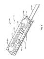
- FIG. 6illustrates a front face 500 A of an example 500 of the first connector 102 .
- FIG. 7illustrates a back face 500 B of connector 500 .
- the first connector 102may be any suitable connector component configured to provide a zero-insertion or low-insertion EHF connection interface for a corresponding connector component on another device or system.
- the first connector 102may include two magnets, 502 A and 502 B.
- the first connector 102may further include the first EHF communication unit 206 , the third communication unit 214 , the connector PCB 216 , the connector body 220 , the first connector alignment element 218 , and/or one or more LED indicators 222 A-N.
- the first connector 102may be electrically and physically connected to a cable 504 .
- the connector body 222may serve as a housing or container for other components of the first connector 102 .
- the connector body 222may encapsulate the PCB 216 , the first EHF communication unit 206 , the third EHF communication unit 214 , and one or more LED indicators 220 A-N using a suitable dielectric material or materials such as plastic.
- the connector body 222may also be sized and configured to allow convenient manipulation by a user.
- the magnets 502 A and 502 Bmay be at least partially housed in the connector body 222 and may be mounted such that both magnets 502 A- 502 B may flush with the mating surface 506 of the connector body 222 .
- the mating surface 506may be configured to provide a suitable physical coupling surface with a corresponding connector on a corresponding device such as the external device 602 shown in FIG. 9 .
- the mating surface 506is coplanar with a surface of the external device 602 .
- the mating surface 506is curved.
- the mating surface 506may include the first connector alignment element 218 .
- the first connector alignment element 218may be a protrusion, ridge, knob, bevel, pin, recess, or other member configured to mate with a corresponding alignment element on a corresponding second connector face 304 (or connector surface 604 of the external device 602 ), to provide physical alignment feedback to the user.
- the second connector face 304(or connector surface 604 of the external device 602 ) may be a target connection region for the first connector 102 .
- the magnets 502 A and 502 Bmay be any suitable magnetic components configured to non-destructively releasably hold the first connector 102 in aligned proximity to the second connector face 304 (or the connector surface 604 of the external device 602 ).
- the magnets 502 A- 502 Bmay be referred as first connector magnets 502 A- 502 B without changing its meaning.
- the second connector 104may be a part of the external device 602 .
- the second connector 104may include at least two magnets (or second connector magnets), such as shown in FIGS. 9A-9D .
- the alignment and proximitymay refer to the alignment and proximity of corresponding EHF communication unit (e.g. 206 ), which must be substantially aligned and in close enough proximity to enable communication between a given pair of EHF communication units.
- the magnets 502 A, 502 Bare one or a combination of permanent magnets, electromagnets, or be formed of ferrous material capable of being magnetically attracted to magnets.
- the first EHF communication unit 206 and the third EHF communication unit 214may be mounted on the connector PCB 216 . In some embodiments, more or fewer EHF communication units may be provided in the first connector 102 or the PCB 216 .
- the first EHF communication unit 206may be mounted on the PCB 216 in an orientation that is orthogonal to that of the third EHF communication unit 214 , to take advantage of polarization effects. Orthogonal orientation may allow the EHF communication units (e.g. 206 or 214 ) to be mounted closely together, because orthogonal EHF signals may not substantially interfere with each other.
- the connector PCB 216 and related circuitsmay be electrically connected to the cable 504 to allow the first connector 102 to obtain power and/or informational signals from a source outside of the first connector 102 .
- the cable 504may provide the first connector 102 with electrical power as well as providing a signal path to and/or from a personal computer or other associated device.
- a first magnet of the first connector magnets 502 A and 502 Bmay be electrically connected to a power conductor in the cable 504
- a second magnet of the first connector magnets 502 A and 502 Bmay be connected to a circuit ground.
- This configurationmay allow power to be provided to the external device 602 through the magnets 502 A and 502 B.
- the magnets 502 A- 502 Bmay be shaped accordingly to provide a suitable electrical interface when aligned and mated with the connector surface 604 of the external device 602 .
- the magnets 502 A and 502 Bmay have protrusions to provide controlled point connections and to avoid “a-spot” problems inherent in flat connector surfaces.
- One or more LED indicators 220 A-Nmay be mounted in or on the first connector 102 to provide visual feedback to the user.
- the LED indicators 220 A-Nmay be electrically connected to the connector PCB 216 and may provide indication of a connector, connection status, or signal transmission status.
- the LED indicators 220 A-Nmay blink or light up if the connector 102 is receiving power and to confirm a proper or correct connection.
- a green LED indicator 220 Nmay light up if the connector 102 is properly aligned and affixed to the connector surface 604 of the external device 602 .
- FIG. 6is an isometric view of a connector system 600 including the first connector 102 or 500 proximate to the second connector 104 or 600 .
- the external device 602may include the second connector (such as connector 104 ) having a second housing 614 defining a second connector face or connector surface 604 configured to be positioned in at least one of a first position and a second position proximate to the first connector face 616 .
- the first and second connectorscan be placed together in a first position with EHF communication unit 206 aligned with EHF communication unit 610 and EHF communication unit 214 aligned with EHF communication unit 608 , or in a second position that is the reverse.
- the external device 602may include an external device PCB 606 with two EHF communication units 608 and 610 disposed near an edge 612 of the external device 602 .
- the EHF communication units of the external device 602may be referred as a second EHF communication unit 608 and a fourth EHF communication unit 610 .
- more or fewer EHF communication unitsmay be provided.
- the second EHF communication unit 608may be configured to communicate with the first EHF communication unit 206 over a first channel when the first connector face 616 is positioned in at least one of the first position and the second position relative to the second connector face 604 .
- the connector surface 604 and second connector face 604may be used interchangeably without changing their meaning.
- the connector surface 604 at the edge 612may include portions made of ferrous material or any other material that provides a magnetically attractive surface to which the first connector magnets 502 A- 502 B may attach.
- the first magnet 502 Amay have a magnet face that is aligned with the first connector face 616 .
- placing the first connector 102 near the connector surface 604 of the external device 602may cause the magnets 502 A and 502 B to be attracted to the connector surface 604 , pulling the connector 102 into proper position and alignment to allow the first EHF communication unit 206 , the third EHF communication unit 214 , the second EHF communication unit 608 , and the fourth EHF communication unit 610 to align and communicate.
- the first connector magnets 502 A and 502 Bmay be connected to a power-providing circuit, this attraction and holding of the first connector 102 may also facilitate electrical power conduction.
- the second connector 104 of the external device 602may include a second magnet (similar to magnet 308 ) disposed in the second housing 614 of the external device 602 .
- the second magnetmay be disposed in the second housing 614 relative to the second connector face 604 .
- the second magnetmay be configured not to align with and not to repel the second magnet when the first connector face 616 is positioned in the first position relative to the second connector face 604 .
- the second magnetis configured to align with and repel the first magnet when the first connector face 616 is positioned in the second position relative to the second connector face 604 .
- the first connector 102may include the first magnetic element ( 502 B) disposed in the first housing 202 relative to the first connector face 616 (or 204 ) and spaced from the first magnet 502 A (or 208 ).
- the first magnetic element ( 502 B)may be configured to align with and attract the second magnet (e.g. magnet 308 ) when the first connector face 616 is positioned in the first position relative to the second connector face 604 .
- the first magnetic element 218may be at least one of a permanent magnet, an electromagnet, and a ferromagnetic element.
- the first magnetic element (or magnet 502 B)may be a third magnet 212 of the first connector 102 .
- the first magnet 502 A (or 208 ) and the third magnet 502 B (or 212 )may have opposite magnetic polarities at the first connector face 616 .
- the second connector 104 of the external device 602may include a fourth magnet (not shown in FIG. 6 , but it is similar to fourth magnet 308 of FIG. 3 ) disposed in the second housing 614 relative to the second connector face 604 .
- the fourth magnetmay be configured to align with and to attract the first magnet 208 when the first connector face 616 is positioned in the first position relative to the second connector face 604 .
- the fourth magnet(such as magnet 308 ) may be configured to align with and repel the third magnet when the first connector face 616 is positioned in the second position relative to the second connector face 604 .
- the second connector 104may further include the second magnetic element (such as one of the magnets 502 C- 502 D) disposed in the second housing 614 relative to the second connector face 604 .
- the second magnetic element(such as one of the second connector magnets shown in FIGS. 9A-9D ) may be configured to align with and be attracted to the first magnet when the first connector face is positioned in the first connector face 616 is positioned in the first position relative to the second connector face 604 .
- the first magnetic element and the second magnetic elementmay include respective ferromagnetic elements.
- the first connector 102may further include the third EHF communication unit 214 disposed in the first housing 202 relative to the first connector face 616 (or 204 ).
- the second connector 104may further include the fourth EHF communication unit 310 disposed in the second housing 614 (or 304 ) relative to the second connector face 604 .
- the third EHF communication unit 214may be configured to communicate with the fourth EHF communication unit 310 when the first connector face 616 is positioned in the at least one of the first position and the second position relative to the second connector face 604 .
- FIGS. 9A-9Dillustrate exemplary configurations of magnetic components of the connector system 600 including the first connector 102 and the second connector 104 of FIGS. 1-3 .
- the connector surface 604may include one or more magnets 502 C and 502 D. Including the magnets 502 C and 502 D at or near the connector surface 604 of the external device 602 allows additional functionality and additional haptic feedback to a user. Further, the magnets 502 A- 502 B (or first connector magnets) may be configured to provide a ground connection in the electrical circuit and may be configured to form in combination an electromagnetic shield around the first EHF communication unit 206 and the third EHF communication unit 214 .
- Each of the first connector magnets 502 A- 502 Bmay have a first pole of a first polarity and a second pole of a second polarity opposite of the first polarity, and the respective first poles of the first connector magnets 502 A- 502 B may be oriented in the same direction.
- each second connector magnets 502 C- 502 Dmay have a first pole of a first polarity and a second pole of a second polarity opposite of the first polarity, and the respective first poles of the second connector magnets 502 C- 502 D may be oriented in the same direction.
- various alignments of the poles of magnets 502 A, 502 B, 502 C, and 502 Dmay be possible. These alignments and combinations of alignments may allow tactile feedback regarding proper alignment and positioning of the first connector 102 at the connector surface based on the attraction or repulsion of the aligned magnet pairs.
- a connector systemmay be configured such that the first connector 102 may connect in either of two orientations.
- poles of one set of magnetsare aligned and presented to opposing poles of another aligned set of magnets.
- magnets 502 A and 502 Bmay always present their south poles to the magnets 502 C and 502 D.
- the magnets 502 C and 502 Dmay always present their north poles. In this configuration, the magnets may always attract each other in both positions of connector 102 relative to connector 104 as long as the opposite magnet pairs are placed in approximate physical alignment.
- a connector systemmay instead be configured with the same poles of each set of magnets facing each other, such that the first connector 102 may always be repelled.
- the magnets 502 A and 502 Bmay present their south poles to the magnets 502 C and 502 D.
- the magnets 502 C and 502 Dmay also present their south poles, thus repelling the magnets 502 A and 502 B and thereby associated first connector 102 .
- Thismay be desirable, for example, if there are two possible connector surfaces 604 on the external device 602 .
- the connectorsmay be configured so that each is only attracted to a corresponding mate, and repelled by the other candidate.
- FIGS. 9C and 9Dshow yet another possible configuration where magnetic poles within each set of magnets on a connector are aligned in opposite directions.
- one of magnets 502 A and 502 Bmay be present a north pole while the other magnet presents a south pole.
- the magnets 502 C and 502 Dmay similarly present the opposing poles such that the magnets attract when the second connector 104 is in the proper orientation and repel when the second connector 104 is not in the proper orientation relative to first connector 102 .
- the first connector 102may therefore only connect in one orientation or position of the two orientations or positions in which the opposing magnet pairs are aligned. All of these configurations provide tactile feedback to the user attempting to connect the connectors together.
- FIG. 10is a block diagram of an illustrative connector 800 having one or more electromagnetic components. Additional feedback and functionality may be possible by using one or more electromagnets for the various magnets ( 502 A-D) already described.
- the external devicesuch as device 602
- the first magneti.e. magnet 502 A
- the electromagnet controller 804may be configured to alternatingly activate and either deactivate or reverse activate the electromagnets 802 A- 802 B or 502 A, thereby producing vibration of the first connector 102 .
- electromagnetsmay allow the an external device 602 to selectively enable or disable the magnetic attraction of its connector surface or surfaces 604 , as well as possibly reversing polarity of any given electromagnet.
- the electromagnet controller 804may be configured to eject the first connector 102 by reversing polarity or by turning the electromagnets off.
- the connector surfaces 604 (or 616 )may be selectively enabled, disabled, and/or configured with a certain polarity combination.
- the electromagnet controller 804may also cause electromagnets 802 A and/or 802 B to vibrate or buzz based on certain predetermined conditions.
- the electromagnets 802 A, 802 B, and/or electromagnet controller 804may be disposed in the first connector 102 , or in both connectors.
- one or more magnetic components on a connectormay be electromagnets.
- the magnets 502 A- 502 B of the first connectormay act as electromagnets and may be controlled by the electromagnet controller 804 .
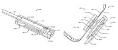
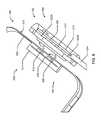
- FIG. 11shows an illustrative first connector 102 and an illustrative mechanical connector 900 .
- FIG. 11shows that the first connector 102 in the form shown similar to connector 500 and having an alignment element 218 in the form of an elongate ridge with spaced-apart magnets 208 and 212 , such as magnets 502 A and 502 B, requires significantly less physical insertion to connect with a complementary connector 104 or 600 than mechanical connector 900 , which would require insertion into a complementary receptacle having aligned conductors to establish a conductive signal and/or power path.
- a first connectorcomprises a housing defining a first connector face configured to be positioned in at least one of a first position and a second position proximate to a second connector face of a second connector; a first extremely high frequency (EHF) communication unit disposed in the housing relative to the first connector face for communicating with a second EHF communication unit of the second connector when the first connector face is positioned in at least one of the first position and the second position relative to the second connector face; and a first magnet disposed in the housing relative to the first connector face, the first magnet configured to align with and repel a second magnet disposed relative to the second connector face when the first connector face is positioned in the second position relative to the second connector face, and the first magnet is configured not to align with and not to repel the second magnet when the first connector face is positioned in the first position relative to the second connector face.
- EHFextremely high frequency
- the first connectormay further comprise a first magnetic element disposed in the housing relative to the first connector face and spaced from the first magnet, wherein the first magnetic element is configured to align with and attract the second magnet when the first connector face is positioned in the first position relative to the second connector face.
- the first magnetic elementmay be at least one of a permanent magnet, an electromagnet, and a ferromagnetic element.
- the first magnetic elementmay be a third magnet, and the first magnet and the third magnet may have opposite magnetic polarities at the first connector face.
- the first connectormay further comprise a third EHF communication unit configured to communicate with a fourth EHF communication unit of the second connector when the first connector face is positioned in the at least one of the first position and the second position relative to the second connector face.
- the first connectormay further comprise a connector printed circuit board (PCB) supported in the housing; a first connector alignment element configured to mate with a complementary second connector alignment element of the second connector, wherein the first connector alignment element matingly receives the second connector alignment element when the first connector face is positioned in the first position and in the second position relative to the second connector face for providing physical alignment feedback to a user; a signal indication circuit having one or more light emitting diode (LED) indicators responsive to an electrical signal transmitted between the first and second EHF communications units; and a connector body disposed in the housing and configured to encapsulate the connector PCB and the first EHF communication unit.
- PCBconnector printed circuit board
- the first EHF communication unitmay be electrically and physically connected to a cable configured to receive at least one of power and one or more informational signals from an external source.
- the first magnetmay have a magnet face that is aligned with the first connector face.
- the first connectormay further comprise an electromagnet controller, wherein the first magnet is an electromagnet configured to be selectively activated by the electromagnet controller, the electromagnet controller is configured to alternatingly activate and either deactivate or reverse activate the electromagnet thereby producing vibration of the first connector.
- a connector systemmay comprise a first connector including a first housing defining a first connector face; a first extremely high frequency (EHF) communication unit disposed in the first housing relative to the first connector face; and a first magnet disposed in the first housing relative to the first connector face; and a second connector including a second housing defining a second connector face configured to be positioned in at least one of a first position and a second position proximate to the first connector face; a second EHF communication unit configured to communicate with the first EHF communication unit over a first channel when the first connector face is positioned in at least one of the first position and the second position relative to the second connector face; and a second magnet disposed in the second housing relative to the second connector face, the second magnet being configured not to align with and not to repel the second magnet when the first connector face is positioned in the first position relative to the second connector face, and the second magnet is configured to align with and repel the first magnet when the first connector face is positioned in the second position relative to the second connector face.
- EHFextremely high frequency
- the second connectormay comprise a fourth magnet disposed in the second housing relative to the second connector face.
- the fourth magnetmay be configured to align with and to attract the first magnet when the first connector face is positioned in the first position relative to the second connector face; and align with and repel the third magnet when the first connector face is positioned in the second position relative to the second connector face.
- the second connectorcomprises a second magnetic element disposed in the second housing relative to the second connector face, wherein the second magnetic element is configured to align with and be attracted to the first magnet when the first connector face is positioned in the first position relative to the second connector face.
- the first magnetic element and the second magnetic elementcomprise respective ferromagnetic elements.
- the first connectormay further comprise a third EHF communication unit disposed in the first housing relative to the first connector face
- the second connectormay further comprise a fourth EHF communication unit disposed in the second housing relative to the second connector face.
- the third EHF communication unitmay be configured to communicate with the fourth EHF communication unit when the first connector face is positioned in the at least one of the first position and the second position relative to the second connector face.
- the first connectormay further comprise a connector printed circuit board (PCB) supported in the first housing; a first connector alignment element configured to mate with a complementary second connector alignment element of the second connector, wherein the first connector alignment element matingly receives the second connector alignment element when the first connector face is positioned in at least one of the first position and the second position relative to the second connector face for providing physical alignment feedback to a user; a signal indication circuit having one or more light emitting diode (LED) indicators responsive to an electrical signal transmitted between the first and second EHF communications units; and a connector body disposed in the first housing and configured to encapsulate the connector PCB and the first EHF communication unit.
- PCBconnector printed circuit board
- a connector systemmay comprise a first connector including a first housing; a first EHF communication unit supported in the first housing; a third EHF communication unit supported in the second housing; and at least two first connector magnets supported in the first housing; and a second connector configured to couple with the first connector.
- the second connectormay comprise a second housing defining a second connector face configured to be positioned in at least one of a first position and a second position proximate to the first connector face; a second EHF communication unit supported in the second housing and configured to communicate with the first EHF communication unit over a first channel; a fourth EHF communication unit supported in the second housing and configured to communicate with the third EHF communication unit on a second channel; and at least two second connector magnets supported in the second housing.
- Polarities of the at least two first connector magnets, and the at least two second connector magnetsmay be oriented such that the first connector couples with the second connector in a desired connector orientation and is held in a coupled state by attraction of the first magnet of the at least two first connector magnets to the first magnet of the at least two second connect magnets and attraction of the second magnet of the first connector magnets to the second magnet of the second connector magnets.
- the first EHF communication unitmay comprise at least one of an insulating material, a chip having an integrated circuit (IC), and an antenna capable of communicating with the IC, further wherein the antenna is fixed at a location by the insulating material.
- ICintegrated circuit
- the first magnet of the at least two first connector magnets and the at least two second connector magnetsmay be electrically conductive, and in electrical contact when the first connector couples with the second connector in the desired connector orientation.
- the first magnet of the at least two first connector magnets and the at least two second connector magnetsform a first path of electrical current in an electrical circuit in the first and second connectors.
- the second magnet of the at least two first connector magnets and second magnet of the at least two second connector magnetsmay be electrically conductive and in electrical contact when the first connector couples with the second connector in the desired connector orientation.
- the second magnet of the at least two first connector magnets and the second magnet of the at least two second connector magnetsmay form a second path of electrical current in the electrical circuit in the first connector and the second connector.
- the at least two first connector magnetsmay be configured to provide a ground connection in the electrical circuit and may be configured to form in combination an electromagnetic shield around the first EHF communication unit and the third EHF communication unit.
- the first connectormay be electrically and physically connected to a cable to obtain at least one of power and one or more informational signals from an external source.
- Each of the at least two first connector magnetsmay have a first pole of a first polarity and a second pole of a second polarity opposite of the first polarity, and the respective first poles of the at least two first connector magnets may be oriented in the same direction.
- Each of the at least two second connector magnetshas a first pole of a first polarity and a second pole of a second polarity opposite of the first polarity, and the respective first poles of the at least two second connector magnets are oriented in the same direction.
- the connector systemmay further comprise an electromagnet controller, wherein the first magnet is an electromagnet configured to be selectively activated by the electromagnet controller, the electromagnet controller is configured to alternatingly activate and either deactivate or reverse activate the electromagnet, thereby producing vibration of the first connector.
- the first housingmay have a first connector face that faces the second connector when the first connector couples with the second connector in the desired connector orientation, and each of the first magnet and second magnet may comprise a magnet face that is aligned with the first connector face.
Landscapes
- Details Of Connecting Devices For Male And Female Coupling (AREA)
Abstract
Description
Claims (31)
Priority Applications (30)
| Application Number | Priority Date | Filing Date | Title |
|---|---|---|---|
| US13/713,564US8794980B2 (en) | 2011-12-14 | 2012-12-13 | Connectors providing HAPTIC feedback |
| US13/760,089US9191263B2 (en) | 2008-12-23 | 2013-02-06 | Contactless replacement for cabled standards-based interfaces |
| US13/776,727US9219956B2 (en) | 2008-12-23 | 2013-02-26 | Contactless audio adapter, and methods |
| PCT/US2013/027835WO2013130486A1 (en) | 2012-03-02 | 2013-02-27 | Contactless replacement for cabled standards-based interfaces |
| CN201380019743.7ACN104541254B (en) | 2012-03-02 | 2013-02-27 | For the contactless replacement of the measured interface of cable type |
| EP13754591.9AEP2820551B1 (en) | 2012-03-02 | 2013-02-27 | Contactless replacement for cabled standards-based interfaces |
| KR1020147027782AKR102033195B1 (en) | 2012-03-02 | 2013-02-27 | Contactless replacement for cabled standards-based interfaces |
| TW102107292ATWI597948B (en) | 2012-03-02 | 2013-03-01 | Non-contact replacement for cable-based standards-based interfaces |
| EP13763793.0AEP2828993B1 (en) | 2012-03-22 | 2013-03-22 | Contactless data transfer systems and methods |
| PCT/US2013/033394WO2013142745A1 (en) | 2012-03-22 | 2013-03-22 | Contactless data transfer systems and methods |
| KR1020147029611AKR101881629B1 (en) | 2012-03-22 | 2013-03-22 | Contactless data transfer systems and methods |
| US13/848,735US9960820B2 (en) | 2008-12-23 | 2013-03-22 | Contactless data transfer systems and methods |
| CN201380025960.7ACN104604164B (en) | 2012-03-22 | 2013-03-22 | Contactless data transmission system and method |
| CN201380047942.9ACN104756411B (en) | 2012-09-14 | 2013-08-17 | Smart Connectors and associated communication links |
| KR1020157009223AKR102095319B1 (en) | 2012-09-14 | 2013-08-17 | Smart connectors and associated communications links |
| CN201710766860.XACN107888234B (en) | 2012-09-14 | 2013-08-17 | Method for providing application support for a first device host system and first device |
| EP13845508.4AEP2896148B1 (en) | 2012-09-14 | 2013-08-17 | Smart connectors and associated communications links |
| PCT/US2013/055487WO2014058534A1 (en) | 2012-09-14 | 2013-08-17 | Smart connectors and associated communications links |
| US13/969,565US9474099B2 (en) | 2008-12-23 | 2013-08-17 | Smart connectors and associated communications links |
| US14/451,427US8939773B2 (en) | 2011-12-14 | 2014-08-04 | Connectors providing haptic feedback |
| US14/596,172US9197011B2 (en) | 2011-12-14 | 2015-01-13 | Connectors providing haptic feedback |
| US14/885,263US9525463B2 (en) | 2008-12-23 | 2015-10-16 | Contactless replacement for cabled standards-based interfaces |
| US14/958,122US9565495B2 (en) | 2008-12-23 | 2015-12-03 | Contactless audio adapter, and methods |
| US15/290,262US9954579B2 (en) | 2008-12-23 | 2016-10-11 | Smart connectors and associated communications links |
| US15/380,457US9819397B2 (en) | 2008-12-23 | 2016-12-15 | Contactless replacement for cabled standards-based interfaces |
| US15/421,181US10142728B2 (en) | 2008-12-23 | 2017-01-31 | Contactless audio adapter, and methods |
| US15/811,051US10236938B2 (en) | 2008-12-23 | 2017-11-13 | Contactless replacement for cabled standards-based interfaces |
| US15/960,105US10588002B2 (en) | 2008-12-23 | 2018-04-23 | Smart connectors and associated communications links |
| US15/966,711US10601470B2 (en) | 2008-12-23 | 2018-04-30 | Contactless data transfer systems and methods |
| US16/197,247US10595124B2 (en) | 2008-12-23 | 2018-11-20 | Full duplex contactless communication systems and methods for the use thereof |
Applications Claiming Priority (2)
| Application Number | Priority Date | Filing Date | Title |
|---|---|---|---|
| US201161570707P | 2011-12-14 | 2011-12-14 | |
| US13/713,564US8794980B2 (en) | 2011-12-14 | 2012-12-13 | Connectors providing HAPTIC feedback |
Related Parent Applications (6)
| Application Number | Title | Priority Date | Filing Date |
|---|---|---|---|
| US13/427,576Continuation-In-PartUS9444146B2 (en) | 2008-12-23 | 2012-03-22 | Integrated circuit with electromagnetic communication |
| US13/524,956Continuation-In-PartUS9322904B2 (en) | 2008-12-23 | 2012-06-15 | Proximity sensing using EHF signals |
| US13/541,543Continuation-In-PartUS20120295539A1 (en) | 2008-12-23 | 2012-07-03 | Ehf communication with electrical isolation and with dielectric transmission medium |
| US13/657,482Continuation-In-PartUS9407311B2 (en) | 2008-12-23 | 2012-10-22 | Contactless signal splicing using an extremely high frequency (EHF) communication link |
| US13/760,089Continuation-In-PartUS9191263B2 (en) | 2008-12-23 | 2013-02-06 | Contactless replacement for cabled standards-based interfaces |
| US13/776,727Continuation-In-PartUS9219956B2 (en) | 2008-12-23 | 2013-02-26 | Contactless audio adapter, and methods |
Related Child Applications (6)
| Application Number | Title | Priority Date | Filing Date |
|---|---|---|---|
| US12/655,041Continuation-In-PartUS8554136B2 (en) | 2008-12-23 | 2009-12-21 | Tightly-coupled near-field communication-link connector-replacement chips |
| US13/524,956Continuation-In-PartUS9322904B2 (en) | 2008-12-23 | 2012-06-15 | Proximity sensing using EHF signals |
| US13/541,543Continuation-In-PartUS20120295539A1 (en) | 2008-12-23 | 2012-07-03 | Ehf communication with electrical isolation and with dielectric transmission medium |
| US13/760,089Continuation-In-PartUS9191263B2 (en) | 2008-12-23 | 2013-02-06 | Contactless replacement for cabled standards-based interfaces |
| US13/969,565Continuation-In-PartUS9474099B2 (en) | 2008-12-23 | 2013-08-17 | Smart connectors and associated communications links |
| US14/451,427ContinuationUS8939773B2 (en) | 2011-12-14 | 2014-08-04 | Connectors providing haptic feedback |
Publications (2)
| Publication Number | Publication Date |
|---|---|
| US20130157477A1 US20130157477A1 (en) | 2013-06-20 |
| US8794980B2true US8794980B2 (en) | 2014-08-05 |
Family
ID=47459179
Family Applications (3)
| Application Number | Title | Priority Date | Filing Date |
|---|---|---|---|
| US13/713,564Active2033-03-29US8794980B2 (en) | 2008-12-23 | 2012-12-13 | Connectors providing HAPTIC feedback |
| US14/451,427ActiveUS8939773B2 (en) | 2011-12-14 | 2014-08-04 | Connectors providing haptic feedback |
| US14/596,172ActiveUS9197011B2 (en) | 2011-12-14 | 2015-01-13 | Connectors providing haptic feedback |
Family Applications After (2)
| Application Number | Title | Priority Date | Filing Date |
|---|---|---|---|
| US14/451,427ActiveUS8939773B2 (en) | 2011-12-14 | 2014-08-04 | Connectors providing haptic feedback |
| US14/596,172ActiveUS9197011B2 (en) | 2011-12-14 | 2015-01-13 | Connectors providing haptic feedback |
Country Status (7)
| Country | Link |
|---|---|
| US (3) | US8794980B2 (en) |
| EP (1) | EP2792031B1 (en) |
| JP (1) | JP6435194B2 (en) |
| KR (1) | KR102030203B1 (en) |
| CN (2) | CN107257051B (en) |
| TW (3) | TWI622232B (en) |
| WO (1) | WO2013090625A1 (en) |
Cited By (28)
| Publication number | Priority date | Publication date | Assignee | Title |
|---|---|---|---|---|
| US20150063746A1 (en)* | 2013-09-02 | 2015-03-05 | Fujitsu Limited | Optical waveguide substrate and information processing device |
| US20150126047A1 (en)* | 2011-12-14 | 2015-05-07 | Keyssa, Inc. | Connectors Providing Haptic Feedback |
| US20150194764A1 (en)* | 2012-07-31 | 2015-07-09 | Hewlett-Packard Development Company, L.P. | Magnetic connector for a computing device |
| US20150236445A1 (en)* | 2013-04-30 | 2015-08-20 | Acer Incorporated | Portable electronic device assembly |
| US20150303619A1 (en)* | 2012-12-21 | 2015-10-22 | Koninklijke Philips N.V. | Magnetic connector assembly |
| US9203597B2 (en) | 2012-03-02 | 2015-12-01 | Keyssa, Inc. | Systems and methods for duplex communication |
| US9322904B2 (en) | 2011-06-15 | 2016-04-26 | Keyssa, Inc. | Proximity sensing using EHF signals |
| US9374154B2 (en) | 2012-09-14 | 2016-06-21 | Keyssa, Inc. | Wireless connections with virtual hysteresis |
| US9379450B2 (en) | 2011-03-24 | 2016-06-28 | Keyssa, Inc. | Integrated circuit with electromagnetic communication |
| US9407311B2 (en) | 2011-10-21 | 2016-08-02 | Keyssa, Inc. | Contactless signal splicing using an extremely high frequency (EHF) communication link |
| US9426660B2 (en) | 2013-03-15 | 2016-08-23 | Keyssa, Inc. | EHF secure communication device |
| US9515365B2 (en) | 2012-08-10 | 2016-12-06 | Keyssa, Inc. | Dielectric coupling systems for EHF communications |
| US9515859B2 (en) | 2011-05-31 | 2016-12-06 | Keyssa, Inc. | Delta modulated low-power EHF communication link |
| US9531425B2 (en) | 2012-12-17 | 2016-12-27 | Keyssa, Inc. | Modular electronics |
| US9553616B2 (en) | 2013-03-15 | 2017-01-24 | Keyssa, Inc. | Extremely high frequency communication chip |
| US9577372B1 (en)* | 2015-09-30 | 2017-02-21 | Western Digital Technologies, Inc. | Magnetic reversible power and data connector |
| US20170099082A1 (en)* | 2008-12-23 | 2017-04-06 | Keyssa, Inc. | Contactless replacement for cabled standards-based interfaces |
| US20170149112A1 (en)* | 2013-08-13 | 2017-05-25 | Keyssa, Inc. | Contactless communication unit connector assemblies |
| US20170179641A1 (en)* | 2015-12-16 | 2017-06-22 | Lenovo (Beijing) Limited | Electronic devices and connectors |
| US9853696B2 (en) | 2008-12-23 | 2017-12-26 | Keyssa, Inc. | Tightly-coupled near-field communication-link connector-replacement chips |
| US20180175548A1 (en)* | 2016-12-16 | 2018-06-21 | Foxconn Interconnect Technology Limited | Alignment structures for chip modules |
| US10049801B2 (en) | 2015-10-16 | 2018-08-14 | Keyssa Licensing, Inc. | Communication module alignment |
| US10236627B1 (en)* | 2018-06-01 | 2019-03-19 | Christmas Northeast, Inc. | Electrical connectors for lighting and the like |
| US10381774B2 (en) | 2016-03-08 | 2019-08-13 | Christmas Northeast, Inc. | Easily installed versatile electrical access system using magnetic electrical connectors |
| US10396492B2 (en) | 2017-02-20 | 2019-08-27 | Christmas Northeast, Inc. | Electric power distribution using magnetic electrical connectors |
| US10411401B1 (en) | 2018-06-01 | 2019-09-10 | Christmas Northeast, Inc. | Electrical junction receptacle for magnetic electrical connectors |
| US10595124B2 (en) | 2008-12-23 | 2020-03-17 | Keyssa, Inc. | Full duplex contactless communication systems and methods for the use thereof |
| US20240128682A1 (en)* | 2022-10-13 | 2024-04-18 | Michael Sansur | Magnetically Coupled Circuits |
Families Citing this family (33)
| Publication number | Priority date | Publication date | Assignee | Title |
|---|---|---|---|---|
| US9614590B2 (en) | 2011-05-12 | 2017-04-04 | Keyssa, Inc. | Scalable high-bandwidth connectivity |
| US8714459B2 (en) | 2011-05-12 | 2014-05-06 | Waveconnex, Inc. | Scalable high-bandwidth connectivity |
| KR101879907B1 (en) | 2011-09-15 | 2018-08-16 | 키사, 아이엔씨. | Wireless communication with dielectric medium |
| EP2769477A1 (en) | 2011-10-20 | 2014-08-27 | Keyssa, Inc. | Low-profile wireless connectors |
| US9559790B2 (en) | 2012-01-30 | 2017-01-31 | Keyssa, Inc. | Link emission control |
| US9344201B2 (en)* | 2012-01-30 | 2016-05-17 | Keyssa, Inc. | Shielded EHF connector assemblies |
| CN104303436B (en) | 2012-03-06 | 2017-04-05 | 凯萨股份有限公司 | System for constraining operating parameters of an EHF communication chip |
| EP2832192B1 (en) | 2012-03-28 | 2017-09-27 | Keyssa, Inc. | Redirection of electromagnetic signals using substrate structures |
| CN104321930A (en) | 2012-04-17 | 2015-01-28 | 凯萨股份有限公司 | Dielectric lens structures for interchip communication |
| KR101449197B1 (en)* | 2012-12-26 | 2014-10-08 | 현대자동차주식회사 | Magnetic connector apparatus for charging electric vehicle |
| EP2974058B1 (en) | 2013-03-15 | 2020-07-15 | Keyssa, Inc. | Contactless ehf data communication |
| JP2015049717A (en)* | 2013-09-02 | 2015-03-16 | タイコエレクトロニクスジャパン合同会社 | Connector, connector assembly and wireless communication module |
| US9300083B2 (en)* | 2013-09-30 | 2016-03-29 | Apple Inc. | Stackable magnetically-retained connector interface |
| US9252543B2 (en)* | 2014-01-24 | 2016-02-02 | Foxconn Interconnect Technology Limited | Dual orientation connector assembly with interior magnetic component |
| US9526979B2 (en)* | 2014-03-11 | 2016-12-27 | Microsoft Technology Licensing, Llc | Storing state for physical modular toys |
| US9419376B1 (en)* | 2014-04-17 | 2016-08-16 | Google Inc. | Multipurpose, electronically versatile connector for wearable electronics |
| USD776058S1 (en) | 2014-04-17 | 2017-01-10 | Google Inc. | Electrical connector |
| US10369477B2 (en) | 2014-10-08 | 2019-08-06 | Microsoft Technology Licensing, Llc | Management of resources within a virtual world |
| US9696757B2 (en) | 2014-10-08 | 2017-07-04 | Microsoft Corporation | Transfer of attributes between generations of characters |
| TWI693759B (en)* | 2016-01-26 | 2020-05-11 | 英屬開曼群島商鴻騰精密科技股份有限公司 | Connector and assembly having the same |
| TWI719014B (en)* | 2016-03-02 | 2021-02-21 | 英屬開曼群島商鴻騰精密科技股份有限公司 | Connector and wireless transmission module thereof |
| CN107666160A (en)* | 2016-07-29 | 2018-02-06 | 鸿富锦精密电子(天津)有限公司 | Charging device and the charge control system with the charging device |
| US10779801B2 (en) | 2016-09-21 | 2020-09-22 | Clarius Mobile Health Corp. | Ultrasound apparatus with improved heat dissipation and methods for providing same |
| CN108206397B (en) | 2016-12-16 | 2021-12-24 | 富士康(昆山)电脑接插件有限公司 | Connector assembly |
| US9780487B1 (en)* | 2017-02-08 | 2017-10-03 | Delphi Technologies, Inc. | Electrical connector assembly with axial connection assist |
| WO2020019861A1 (en)* | 2018-07-26 | 2020-01-30 | Oppo广东移动通信有限公司 | Electronic device |
| EP3890281B1 (en) | 2018-12-17 | 2023-08-09 | Guangdong Oppo Mobile Telecommunications Corp., Ltd. | Camera mounting module, camera assembly and mobile terminal |
| WO2021262143A1 (en)* | 2020-06-23 | 2021-12-30 | Hewlett-Packard Development Company, L.P. | Input/output ports |
| KR102500798B1 (en)* | 2020-10-21 | 2023-02-16 | 엘아이지넥스원 주식회사 | Connector of electronic equipment, receptacle of connector and plug of connector |
| US11996603B2 (en) | 2022-05-19 | 2024-05-28 | Microsoft Technology Licensing, Llc | Self-aligning magnetic antenna feed connection |
| US20240113774A1 (en)* | 2022-09-30 | 2024-04-04 | Microsoft Technology Licensing, Llc | Data communication connector |
| TWI842128B (en)* | 2022-10-14 | 2024-05-11 | 立錡科技股份有限公司 | Switching regulator and operation clock signal generator circuit and control method thereof |
| WO2025027802A1 (en)* | 2023-08-01 | 2025-02-06 | 任天堂株式会社 | Game device and game system |
Citations (104)
| Publication number | Priority date | Publication date | Assignee | Title |
|---|---|---|---|---|
| US3796831A (en) | 1972-11-13 | 1974-03-12 | Rca Corp | Pulse modulation and detection communications system |
| US4485312A (en) | 1981-06-15 | 1984-11-27 | Tokyo Shibaura Denki Kabushiki Kaisha | Hysteresis circuit |
| US4497068A (en) | 1982-01-25 | 1985-01-29 | Eaton Corporation | Encoding system for optic data link |
| US4694504A (en) | 1985-06-03 | 1987-09-15 | Itt Electro Optical Products, A Division Of Itt Corporation | Synchronous, asynchronous, and data rate transparent fiber optic communications link |
| EP0515187A2 (en) | 1991-05-22 | 1992-11-25 | Wolff Controls Corporation | Method and apparatus for sensing proximity of an object using near-field effects |
| US5543808A (en) | 1995-05-24 | 1996-08-06 | The United States Of America As Represented By The Secretary Of The Army | Dual band EHF, VHF vehicular whip antenna |
| US5621913A (en) | 1992-05-15 | 1997-04-15 | Micron Technology, Inc. | System with chip to chip communication |
| US5754948A (en) | 1995-12-29 | 1998-05-19 | University Of North Carolina At Charlotte | Millimeter-wave wireless interconnection of electronic components |
| US5773878A (en) | 1995-10-28 | 1998-06-30 | Institute Of Microelectronics National University Of Singapore | IC packaging lead frame for reducing chip stress and deformation |
| US5921783A (en)* | 1995-04-01 | 1999-07-13 | Klaus-Dieter Fritsch | Electromechanical connection device |
| US5941729A (en)* | 1997-09-10 | 1999-08-24 | International Business Machines Corporation | Safe-snap computer cable |
| US5956626A (en) | 1996-06-03 | 1999-09-21 | Motorola, Inc. | Wireless communication device having an electromagnetic wave proximity sensor |
| US6351237B1 (en) | 1995-06-08 | 2002-02-26 | Metawave Communications Corporation | Polarization and angular diversity among antenna beams |
| US6490443B1 (en) | 1999-09-02 | 2002-12-03 | Automated Business Companies | Communication and proximity authorization systems |
| US6492973B1 (en) | 1998-09-28 | 2002-12-10 | Sharp Kabushiki Kaisha | Method of driving a flat display capable of wireless connection and device for driving the same |
| US6534784B2 (en) | 2001-05-21 | 2003-03-18 | The Regents Of The University Of Colorado | Metal-oxide electron tunneling device for solar energy conversion |
| US6542720B1 (en) | 1999-03-01 | 2003-04-01 | Micron Technology, Inc. | Microelectronic devices, methods of operating microelectronic devices, and methods of providing microelectronic devices |
| EP1298809A2 (en) | 2001-09-28 | 2003-04-02 | Siemens Information and Communication Mobile LLC | System and method for reducing SAR values |
| US6590544B1 (en) | 1998-09-01 | 2003-07-08 | Qualcomm, Inc. | Dielectric lens assembly for a feed antenna |
| US6607136B1 (en) | 1998-09-16 | 2003-08-19 | Beepcard Inc. | Physical presence digital authentication system |
| US20040214621A1 (en) | 2003-04-25 | 2004-10-28 | Motorola, Inc. | Wireless communication device with variable antenna radiation pattern and corresponding method |
| US20050140436A1 (en) | 2002-07-19 | 2005-06-30 | Micro Mobio | Dual band power amplifier module for wireless communication devices |
| US6915529B1 (en) | 1998-02-27 | 2005-07-05 | Sharp Kabushiki Kaisha | Milliwave transmitting device, milliwave receiving device and milliwave transmission and reception system capable of simplifying wiring of a receiving system of terrestrial broadcasting service and satellite broadcasting service |
| US6967347B2 (en) | 2001-05-21 | 2005-11-22 | The Regents Of The University Of Colorado | Terahertz interconnect system and applications |
| US20060051981A1 (en)* | 2002-09-13 | 2006-03-09 | Hermann Neidlein | Method and device for producing an electrical connection of sub-assemblies and modules |
| US20060159158A1 (en) | 2004-12-22 | 2006-07-20 | Artimi Ltd | Contactless connector systems |
| US20070024504A1 (en) | 2005-07-27 | 2007-02-01 | Kabushiki Kaisha Toshiba | Semiconductor device |
| US20070063056A1 (en) | 2005-09-21 | 2007-03-22 | International Business Machines Corporation | Apparatus and methods for packaging antennas with integrated circuit chips for millimeter wave applications |
| US7213766B2 (en) | 2003-11-17 | 2007-05-08 | Dpd Patent Trust Ltd | Multi-interface compact personal token apparatus and methods of use |
| US20070229270A1 (en) | 2006-03-16 | 2007-10-04 | Broadcom Corporation, A California Corporation | RFID system with RF bus |
| US20070278632A1 (en) | 2006-06-01 | 2007-12-06 | Broadcom Corporation | Leadframe IC packages having top and bottom integrated heat spreaders |
| US7311526B2 (en) | 2005-09-26 | 2007-12-25 | Apple Inc. | Magnetic connector for electronic device |
| US20080089667A1 (en) | 2006-10-13 | 2008-04-17 | Jeff Grady | Interface systems for portable digital media storage and playback devices |
| US20080112101A1 (en) | 2006-11-15 | 2008-05-15 | Mcelwee Patrick T | Transmission line filter for esd protection |
| US20080150821A1 (en) | 2006-12-22 | 2008-06-26 | Sony Deutschland Gmbh | Flexible substrate integrated waveguides |
| US20080150799A1 (en) | 2006-12-21 | 2008-06-26 | Hemmi Christian O | Polarization Control System and Method for an Antenna Array |
| US20080159243A1 (en) | 2006-12-30 | 2008-07-03 | Broadcom Corporation | Local wireless communications within a device |
| US20080195788A1 (en) | 2007-02-12 | 2008-08-14 | Wilocity Ltd. | Wireless Docking Station |
| US20080192726A1 (en) | 2006-11-01 | 2008-08-14 | Kumar Mahesh | Wireless HD MAC frame format |
| US20080290959A1 (en) | 2007-05-22 | 2008-11-27 | Mohammed Ershad Ali | Millimeter wave integrated circuit interconnection scheme |
| US20090006677A1 (en) | 2007-06-28 | 2009-01-01 | Broadcom Corporation | Universal serial bus dongle device with wireless telephony transceiver and system for use therewith |
| US20090009337A1 (en) | 2006-06-21 | 2009-01-08 | Broadcom Corporation | Rfid integrated circuit with integrated antenna structure |
| US20090037628A1 (en) | 2007-07-31 | 2009-02-05 | Broadcom Corporation | Processing system with millimeter wave host interface and method for use therewith |
| US20090075688A1 (en) | 2007-09-18 | 2009-03-19 | Ahmadreza Rofougaran | Method and system for calibrating a power amplifier |
| US7512395B2 (en) | 2006-01-31 | 2009-03-31 | International Business Machines Corporation | Receiver and integrated AM-FM/IQ demodulators for gigabit-rate data detection |
| US20090094506A1 (en) | 2007-10-03 | 2009-04-09 | Qualcomm Incorporated | Millimeter-wave communications for peripheral devices |
| US20090175323A1 (en) | 2008-01-08 | 2009-07-09 | Qualcomm Incorporated | Methods and Devices for Wireless Chip-to-Chip Communications |
| US20090218407A1 (en) | 2008-02-29 | 2009-09-03 | Broadcom Corporation | Integrated circuit with millimeter wave and inductive coupling and methods for use therewith |
| US20090218701A1 (en) | 2008-02-28 | 2009-09-03 | Broadcom Corporation | Inductively coupled integrated circuit with magnetic communication path and methods for use therewith |
| US20090239392A1 (en) | 2008-03-24 | 2009-09-24 | Kabushiki Kaisha Toshiba | Electronic Apparatus |
| US20090236701A1 (en) | 2008-03-18 | 2009-09-24 | Nanyang Technological University | Chip arrangement and a method of determining an inductivity compensation structure for compensating a bond wire inductivity in a chip arrangement |
| US20090239483A1 (en) | 2007-01-31 | 2009-09-24 | Broadcom Corporation | Apparatus for allocation of wireless resources |
| US20090245808A1 (en) | 2008-03-28 | 2009-10-01 | Ahmadreza Rofougaran | Method and system for inter-chip communication via integrated circuit package waveguides |
| US7598923B2 (en) | 2006-05-22 | 2009-10-06 | Sony Corporation | Apparatus and method for communications via multiple millimeter wave signals |
| US7599427B2 (en) | 2005-12-30 | 2009-10-06 | Honeywell International Inc. | Micro range radio frequency (RF) communications link |
| US7612630B2 (en) | 2001-05-08 | 2009-11-03 | Formfactor, Inc. | Electromagnetically coupled interconnect system architecture |
| US20090280765A1 (en) | 2008-05-07 | 2009-11-12 | Ahmadreza Rofougaran | Method And System For On-Demand Filtering In A Receiver |
| US7656205B2 (en) | 2008-01-21 | 2010-02-02 | National Taiwan University | Dual-injection locked frequency dividing circuit |
| US7664461B2 (en) | 2006-03-02 | 2010-02-16 | Broadcom Corporation | RFID reader architecture |
| US20100127804A1 (en) | 2008-11-26 | 2010-05-27 | Nick Vouloumanos | multi-component waveguide assembly |
| US20100159829A1 (en) | 2008-12-23 | 2010-06-24 | Mccormack Gary D | Tightly-coupled near-field communication-link connector-replacement chips |
| US7760045B2 (en) | 2006-05-19 | 2010-07-20 | Sony Corporation | Semiconductor device interconnecting unit, semiconductor device, high-frequency module, and semiconductor device interconnecting method |
| US7761092B2 (en) | 2004-02-06 | 2010-07-20 | Sony Corporation | Systems and methods for communicating with multiple devices |
| US7769347B2 (en) | 2001-05-02 | 2010-08-03 | Trex Enterprises Corp. | Wireless communication system |
| US7768457B2 (en) | 2007-06-22 | 2010-08-03 | Vubiq, Inc. | Integrated antenna and chip package and method of manufacturing thereof |
| US20100202499A1 (en) | 2009-02-06 | 2010-08-12 | National Taiwan University | Wireless radio frequency signal transceiving system |
| US7791167B1 (en) | 2008-02-27 | 2010-09-07 | Broadcom Corporation | Inductively coupled integrated circuit and methods for use therewith |
| US20100231452A1 (en) | 2005-09-23 | 2010-09-16 | California Institute Of Technology | Mm-wave fully integrated phased array receiver and transmitter with on-chip antennas |
| US7820990B2 (en) | 2006-12-11 | 2010-10-26 | Lockheed Martin Corporation | System, method and apparatus for RF directed energy |
| US20100277394A1 (en) | 2007-09-05 | 2010-11-04 | Thomas Haustein | Adaptive Adjustment of an Antenna Arrangement for Exploiting Polarization and/or Beamforming Separation |
| US20100283700A1 (en) | 2009-05-08 | 2010-11-11 | Anokiwave, Inc. | Antennas Using Chip-Package Interconnections for Millimeter-wave Wireless Communication |
| US20100297954A1 (en) | 2009-05-20 | 2010-11-25 | Ahmadreza Rofougaran | Method and system for chip-to-chip mesh networks |
| US20110047588A1 (en) | 2009-08-21 | 2011-02-24 | Sony Corporation | Wired transmission line for AV devices |
| US7907924B2 (en) | 2006-05-19 | 2011-03-15 | Sony Corporation | Semiconductor device interconnecting unit, semiconductor device and high-frequency module having a millimeter wave band |
| EP2309608A1 (en) | 2009-10-09 | 2011-04-13 | Ondal Industrietechnik GmbH | Rotatable electrical coupling and connector therefor |
| US7929474B2 (en) | 2007-06-22 | 2011-04-19 | Vubiq Incorporated | System and method for wireless communication in a backplane fabric architecture |
| EP2360923A1 (en) | 2010-02-24 | 2011-08-24 | Thomson Licensing | Method for selectively requesting adaptive streaming content and a device implementing the method |
| US20110207425A1 (en) | 2009-08-04 | 2011-08-25 | Georgia Tech Research Corporation | Multi-gigabit millimeter wave receiver system and demodulator system |
| US8014416B2 (en) | 2006-02-14 | 2011-09-06 | Sibeam, Inc. | HD physical layer of a wireless communication device |
| WO2011114738A1 (en) | 2010-03-19 | 2011-09-22 | シリコンライブラリ株式会社 | Wireless transmission system and wireless transmitter, wireless receiver, wireless transmission method wireless reception method and wireless communication method used with same |
| WO2011114737A1 (en) | 2010-03-19 | 2011-09-22 | シリコンライブラリ株式会社 | Wireless transmission system and wireless transmitter, wireless receiver, wireless transmission method, wireless reception method and wireless communication method used with same |
| US8041227B2 (en) | 2006-11-16 | 2011-10-18 | Silicon Laboratories Inc. | Apparatus and method for near-field communication |
| US8063769B2 (en) | 2007-03-30 | 2011-11-22 | Broadcom Corporation | Dual band antenna and methods for use therewith |
| US20110285606A1 (en) | 2008-11-19 | 2011-11-24 | Nxp B.V. | Millimetre-wave radio antenna module |
| US20110286703A1 (en) | 2007-10-12 | 2011-11-24 | Sony Corporation | Connector system, connecting cable and receiving tool |
| US8081699B2 (en) | 2006-07-15 | 2011-12-20 | Kazimierz Siwiak | Wireless communication system and method with elliptically polarized radio frequency signals |
| US20110311231A1 (en) | 2009-02-26 | 2011-12-22 | Battelle Memorial Institute | Submersible vessel data communications system |
| US8121542B2 (en) | 2007-10-16 | 2012-02-21 | Rafi Zack | Virtual connector based on contactless link |
| US20120064664A1 (en) | 2010-09-13 | 2012-03-15 | Semiconductor Energy Laboratory Co., Ltd. | Method for manufacturing semiconductor device |
| US20120069772A1 (en) | 2010-09-20 | 2012-03-22 | Research In Motion Limited | Communications system providing mobile wireless communications device application module associations for respective wireless communications formats and related methods |
| US8183935B2 (en) | 2006-10-03 | 2012-05-22 | Milano Alberto | Phased shifted oscilator and antenna |
| US8244179B2 (en) | 2005-05-12 | 2012-08-14 | Robin Dua | Wireless inter-device data processing configured through inter-device transmitted data |
| US8279611B2 (en) | 2009-12-09 | 2012-10-02 | Research In Motion Limited | Flexible cable having rectangular waveguide formed therein and methods of manufacturing same |
| US20120263244A1 (en) | 2011-03-24 | 2012-10-18 | Waveconnex, Inc. | Integrated circuit with electromagnetic communication |
| US20120290760A1 (en) | 2011-05-12 | 2012-11-15 | Waveconnex, Inc. | Scalable high-bandwidth connectivity |
| US20120286049A1 (en) | 2011-05-12 | 2012-11-15 | Waveconnex, Inc. | Scalable high-bandwidth connectivity |
| US20120295539A1 (en) | 2008-12-23 | 2012-11-22 | Waveconnex, Inc. | Ehf communication with electrical isolation and with dielectric transmission medium |
| US20120307932A1 (en) | 2011-05-31 | 2012-12-06 | Waveconnex, Inc. | Delta modulated low power ehf communication link |
| WO2012166922A1 (en) | 2011-05-31 | 2012-12-06 | Waveconnex, Inc. | Delta modulated low power ehf communication link |
| US20120319890A1 (en) | 2011-06-15 | 2012-12-20 | Waveconnex, Inc. | Distance measurement using ehf signals |
| US20130070817A1 (en) | 2011-09-15 | 2013-03-21 | Gary D. McCormack | Wireless communication with dielectric medium |
| WO2012155135A3 (en) | 2011-05-12 | 2013-03-21 | Waveconnex, Inc. | Scalable high-bandwidth connectivity |
| WO2013059801A1 (en) | 2011-10-20 | 2013-04-25 | Waveconnex, Inc. | Low-profile wireless connectors |
| WO2013059802A1 (en) | 2011-10-21 | 2013-04-25 | Waveconnex, Inc. | Contactless signal splicing |
Family Cites Families (142)
| Publication number | Priority date | Publication date | Assignee | Title |
|---|---|---|---|---|
| US2753551A (en) | 1951-06-20 | 1956-07-03 | Raytheon Mfg Co | Circularly polarized radio object locating system |
| DE1081075B (en) | 1956-04-24 | 1960-05-05 | Marie G R P | Dielectric lens |
| US3971930A (en) | 1974-04-24 | 1976-07-27 | The United States Of America As Represented By The Administrator Of The National Aeronautics And Space Administration | Polarization compensator for optical communications |
| JPS5272502A (en) | 1975-12-13 | 1977-06-17 | Mitsubishi Electric Corp | Code transmitter |
| US4678937A (en) | 1984-02-03 | 1987-07-07 | Rosemount Engineering Company Limited | Electrical isolation circuit |
| JP2700553B2 (en) | 1988-03-31 | 1998-01-21 | 株式会社 潤工社 | Transmission circuit |
| US4946237A (en) | 1989-06-30 | 1990-08-07 | At&T Bell Laboratories | Cable having non-metallic armoring layer |
| GB9019489D0 (en) | 1990-09-06 | 1990-10-24 | Ncr Co | Antenna control for a wireless local area network station |
| US5199086A (en) | 1991-01-17 | 1993-03-30 | Massachusetts Institute Of Technology | Electro-optic system |
| JPH05236031A (en) | 1991-07-23 | 1993-09-10 | Hitachi Maxell Ltd | Data transmission system |
| JPH05327788A (en) | 1992-05-15 | 1993-12-10 | Hitachi Maxell Ltd | Data demodulating circuit |
| JPH076817A (en)* | 1993-06-15 | 1995-01-10 | Hitachi Ltd | Connect device |
| US5471668A (en) | 1994-06-15 | 1995-11-28 | Texas Instruments Incorporated | Combined transmitter/receiver integrated circuit with learn mode |
| US5749052A (en) | 1995-05-24 | 1998-05-05 | Tele Digital Development, Inc. | Cellular telephone management system |
| JP3166897B2 (en) | 1995-08-18 | 2001-05-14 | 株式会社村田製作所 | Non-radiative dielectric line and its integrated circuit |
| US5943374A (en) | 1995-12-11 | 1999-08-24 | Hitachi Denshi Kabushiki Kaisha | Out-of-synchronization recovery method and apparatus of data transmission system |
| US5675349A (en) | 1996-02-12 | 1997-10-07 | Boeing North American, Inc. | Durable, lightweight, radar lens antenna |
| US5786626A (en) | 1996-03-25 | 1998-07-28 | Ibm Corporation | Thin radio frequency transponder with leadframe antenna structure |
| US6072433A (en) | 1996-07-31 | 2000-06-06 | California Institute Of Technology | Autonomous formation flying sensor |
| CN1178402A (en)* | 1996-08-09 | 1998-04-08 | 住友电装株式会社 | Charging Connectors for Electric Vehicles |
| JP3786497B2 (en) | 1997-06-13 | 2006-06-14 | 富士通株式会社 | Semiconductor module with built-in antenna element |
| JP3269448B2 (en) | 1997-07-11 | 2002-03-25 | 株式会社村田製作所 | Dielectric line |
| US6947795B2 (en) | 2001-10-01 | 2005-09-20 | Transoma Medical, Inc. | Frame length modulation and pulse position modulation for telemetry of analog and digital data |
| JP3221382B2 (en) | 1997-12-17 | 2001-10-22 | 株式会社村田製作所 | Non-radiative dielectric line and its integrated circuit |
| US7548787B2 (en) | 2005-08-03 | 2009-06-16 | Kamilo Feher | Medical diagnostic and communication system |
| JP3498597B2 (en) | 1998-10-22 | 2004-02-16 | 株式会社村田製作所 | Dielectric line conversion structure, dielectric line device, directional coupler, high frequency circuit module, and transmission / reception device |
| US6373447B1 (en) | 1998-12-28 | 2002-04-16 | Kawasaki Steel Corporation | On-chip antenna, and systems utilizing same |
| US6252767B1 (en) | 1999-06-22 | 2001-06-26 | Hewlett-Packard Company | Low impedance hinge for notebook computer |
| DE19930642A1 (en)* | 1999-07-02 | 2001-01-04 | Magcode Ag | Electromechanical connection device |
| JP3393195B2 (en) | 1999-11-26 | 2003-04-07 | 株式会社ホンダエレシス | Object detection device and occupant detection system |
| US6647246B1 (en) | 2000-01-10 | 2003-11-11 | Industrial Technology Research Institute | Apparatus and method of synchronization using delay measurements |
| JP3932767B2 (en) | 2000-05-12 | 2007-06-20 | 日立電線株式会社 | Array antenna |
| JP2001339207A (en) | 2000-05-26 | 2001-12-07 | Kyocera Corp | Antenna feed line and antenna module using the same |
| US6741646B1 (en) | 2000-07-25 | 2004-05-25 | Thomson Licensing S.A. | Modulation technique for transmitting a high data rate signal, and an auxiliary data signal, through a band limited channel |
| US6901246B2 (en) | 2000-10-06 | 2005-05-31 | Xg Technology, Llc | Suppressed cycle based carrier modulation using amplitude modulation |
| AU783921B2 (en)* | 2000-11-16 | 2005-12-22 | Symbol Technologies, Inc. | Coexistence techniques in wireless networks |
| DE10202480A1 (en) | 2001-01-30 | 2002-08-14 | Infineon Technologies Ag | Signal transfer method for computer, involves converting signal into line-independent electromagnetic wave at transmitter in one electronic module, which is reconverted into reception signal at receiver of other module |
| US7068733B2 (en) | 2001-02-05 | 2006-06-27 | The Directv Group, Inc. | Sampling technique for digital beam former |
| JP2002237036A (en) | 2001-02-08 | 2002-08-23 | Hitachi Ltd | Information recording method, reproduction method and information recording device |
| US6512431B2 (en) | 2001-02-28 | 2003-01-28 | Lockheed Martin Corporation | Millimeterwave module compact interconnect |
| JP2002261514A (en) | 2001-02-28 | 2002-09-13 | Matsushita Electric Ind Co Ltd | NRD guide circuit |
| JP3530829B2 (en) | 2001-03-12 | 2004-05-24 | 日本ピラー工業株式会社 | Fluororesin composition for electronic parts |
| JP2002312000A (en) | 2001-04-16 | 2002-10-25 | Sakai Yasue | Compression method and device, expansion method and device, compression/expansion system, peak detection method, program, recording medium |
| US6531977B2 (en) | 2001-08-03 | 2003-03-11 | Mcewan Technologies, Llc | Pulse center detector for radars and reflectometers |
| JP2003218612A (en) | 2001-11-16 | 2003-07-31 | Murata Mfg Co Ltd | Dielectric line, high frequency circuit, and high frequency circuit apparatus |
| JP3852338B2 (en) | 2002-01-15 | 2006-11-29 | 株式会社Kddi研究所 | Method for disconnecting communication link of mobile station in road-to-vehicle communication system |
| JP4523223B2 (en) | 2002-04-26 | 2010-08-11 | 株式会社日立製作所 | Radar sensor |
| JP4054634B2 (en) | 2002-08-27 | 2008-02-27 | 沖電気工業株式会社 | Semiconductor device |
| US7436876B2 (en) | 2002-11-15 | 2008-10-14 | Time Domain Corporation | System and method for fast acquisition of ultra wideband signals |
| EP1567968B1 (en) | 2002-11-21 | 2006-08-02 | Koninklijke Philips Electronics N.V. | Method of recognizing whether a transponder belongs to a group of transponders |
| JP4514463B2 (en) | 2003-02-12 | 2010-07-28 | パナソニック株式会社 | Transmitting apparatus and wireless communication method |
| US7603710B2 (en) | 2003-04-03 | 2009-10-13 | Network Security Technologies, Inc. | Method and system for detecting characteristics of a wireless network |
| US7113087B1 (en) | 2003-04-08 | 2006-09-26 | Microsoft Corporation | Proximity sensing based on antenna impedance variation |
| US7039397B2 (en) | 2003-07-30 | 2006-05-02 | Lear Corporation | User-assisted programmable appliance control |
| US7228102B2 (en) | 2003-08-05 | 2007-06-05 | Avago Technologie Ecbu Ip (Singapore) Pte. Ltd. | Resonant frequency user proximity detection |
| JP4133747B2 (en) | 2003-11-07 | 2008-08-13 | 東光株式会社 | Input / output coupling structure of dielectric waveguide |
| US20070273476A1 (en) | 2004-03-26 | 2007-11-29 | Semiconductor Energy Laboratory Co., Ltd. | Thin Semiconductor Device And Operation Method Of Thin Semiconductor Device |
| JP4200939B2 (en) | 2004-05-19 | 2008-12-24 | ソニー株式会社 | Wireless communication system, receiving apparatus and receiving method |
| FR2871312B1 (en) | 2004-06-03 | 2006-08-11 | St Microelectronics Sa | CHARGE MODULATION IN AN ELECTROMAGNETIC TRANSPONDER |
| US20060029229A1 (en) | 2004-08-03 | 2006-02-09 | Alexei Trifonov | QKD station with EMI signature suppression |
| GB2419454A (en) | 2004-10-19 | 2006-04-26 | Pranil Ram | Multiple monitor display apparatus |
| US8527003B2 (en) | 2004-11-10 | 2013-09-03 | Newlans, Inc. | System and apparatus for high data rate wireless communications |
| US8060102B2 (en) | 2004-12-14 | 2011-11-15 | Bce Inc. | System and method for coverage analysis in a wireless network |
| US7787562B2 (en) | 2004-12-29 | 2010-08-31 | Motorola, Inc. | Method and apparatus for adaptive modulation of wireless communication signals |
| US7881675B1 (en) | 2005-01-07 | 2011-02-01 | Gazdzinski Robert F | Wireless connector and methods |
| JP3793822B1 (en) | 2005-01-07 | 2006-07-05 | オプテックス株式会社 | Microwave sensor |
| GB0501593D0 (en) | 2005-01-25 | 2005-03-02 | Innovision Res & Tech Plc | Demodulation apparatus and method |
| US7975079B2 (en) | 2005-02-07 | 2011-07-05 | Broadcom Corporation | Computer chip set having on board wireless interfaces to support parallel communication |
| US20060276157A1 (en) | 2005-06-03 | 2006-12-07 | Chen Zhi N | Apparatus and methods for packaging antennas with integrated circuit chips for millimeter wave applications |
| US7352567B2 (en) | 2005-08-09 | 2008-04-01 | Apple Inc. | Methods and apparatuses for docking a portable electronic device that has a planar like configuration and that operates in multiple orientations |
| GB0525635D0 (en) | 2005-12-16 | 2006-01-25 | Innovision Res & Tech Plc | Chip card and method of data communication |
| US20070147425A1 (en) | 2005-12-28 | 2007-06-28 | Wavesat | Wireless modem |
| US8681810B2 (en) | 2006-04-13 | 2014-03-25 | Qualcomm Incorporated | Dynamic carrier sensing thresholds |
| US7467948B2 (en)* | 2006-06-08 | 2008-12-23 | Nokia Corporation | Magnetic connector for mobile electronic devices |
| US7936274B2 (en) | 2006-08-30 | 2011-05-03 | Exponent Inc. | Shield for radio frequency ID tag or contactless smart card |
| JP2008083679A (en) | 2006-08-31 | 2008-04-10 | Seiko Epson Corp | Display device and electronic device |
| JP2008079241A (en) | 2006-09-25 | 2008-04-03 | Sharp Corp | Detection circuit, modulation method determination circuit, integrated circuit, tuner device, and multi-system shared receiver |
| US9697556B2 (en) | 2007-09-06 | 2017-07-04 | Mohammad A. Mazed | System and method of machine learning based user applications |
| GB0700671D0 (en) | 2006-12-15 | 2007-02-21 | Innovision Res & Tech Plc | Nfc communicator and method of data communication |
| US7557303B2 (en) | 2006-12-18 | 2009-07-07 | Lsi Corporation | Electronic component connection support structures including air as a dielectric |
| US8013610B1 (en) | 2006-12-21 | 2011-09-06 | Seektech, Inc. | High-Q self tuning locating transmitter |
| US8350761B2 (en) | 2007-01-04 | 2013-01-08 | Apple Inc. | Antennas for handheld electronic devices |
| JP2008252566A (en) | 2007-03-30 | 2008-10-16 | Matsushita Electric Ind Co Ltd | AV equipment |
| US8351982B2 (en) | 2007-05-23 | 2013-01-08 | Broadcom Corporation | Fully integrated RF transceiver integrated circuit |
| US7743659B2 (en) | 2007-05-25 | 2010-06-29 | The Boeing Company | Structural health monitoring (SHM) transducer assembly and system |
| US7722358B2 (en)* | 2007-06-15 | 2010-05-25 | Microsoft Corporation | Electrical connection between devices |
| TWI337431B (en)* | 2007-07-20 | 2011-02-11 | Asustek Comp Inc | Electronic device having a connector with changeable magnetic guiding pole and connector assembly |
| US7825775B2 (en) | 2007-07-31 | 2010-11-02 | Symbol Technologies, Inc. | Antenna-based trigger |
| US20090086844A1 (en) | 2007-09-28 | 2009-04-02 | Ahmadreza Rofougaran | Method And System For A Programmable Local Oscillator Generator Utilizing A DDFS For Extremely High Frequencies |
| US8244175B2 (en) | 2007-09-28 | 2012-08-14 | Broadcom Corporation | Method and system for signal repeater with gain control and spatial isolation |
| US7881753B2 (en) | 2007-09-28 | 2011-02-01 | Broadcom Corporation | Method and system for sharing multiple antennas between TX and RX in a repeat field of polarization isolation |
| US8023886B2 (en) | 2007-09-28 | 2011-09-20 | Broadcom Corporation | Method and system for repeater with gain control and isolation via polarization |
| US8634767B2 (en) | 2007-09-30 | 2014-01-21 | Broadcom Corporation | Method and system for utilizing EHF repeaters and/or transceivers for detecting and/or tracking an entity |
| US7746256B2 (en) | 2007-10-05 | 2010-06-29 | Infineon Technologies Ag | Analog to digital conversion using irregular sampling |
| US8428528B2 (en) | 2007-10-24 | 2013-04-23 | Biotronik Crm Patent Ag | Radio communications system designed for a low-power receiver |
| US9537566B2 (en) | 2008-01-11 | 2017-01-03 | Alcatel-Lucent Usa Inc. | Realizing FDD capability by leveraging existing TDD technology |
| US8310444B2 (en)* | 2008-01-29 | 2012-11-13 | Pacinian Corporation | Projected field haptic actuation |
| JP4497222B2 (en) | 2008-03-26 | 2010-07-07 | ソニー株式会社 | COMMUNICATION DEVICE, COMMUNICATION METHOD, AND COMPUTER PROGRAM |
| US8416880B2 (en) | 2008-03-31 | 2013-04-09 | Nxp B.V. | Digital modulator |
| US8184651B2 (en) | 2008-04-09 | 2012-05-22 | Altera Corporation | PLD architecture optimized for 10G Ethernet physical layer solution |
| US8755849B2 (en) | 2008-05-07 | 2014-06-17 | Broadcom Corporation | Method and system for power management in a beamforming system |
| CN102067682B (en) | 2008-06-16 | 2014-07-16 | 日本电气株式会社 | Base station control module, wireless base station, base station control device, and base station control method |
| JP4845935B2 (en)* | 2008-07-10 | 2011-12-28 | 日本電信電話株式会社 | Wireless device |
| JP2010103982A (en) | 2008-09-25 | 2010-05-06 | Sony Corp | Millimeter wave transmission device, millimeter wave transmission method, and millimeter wave transmission system |
| US8131645B2 (en) | 2008-09-30 | 2012-03-06 | Apple Inc. | System and method for processing media gifts |
| WO2010042859A1 (en) | 2008-10-10 | 2010-04-15 | Zapmytv.Com, Inc. | Controlled delivery of content data streams to remote users |
| CN102177742B (en) | 2008-10-29 | 2015-04-22 | 马维尔国际贸易有限公司 | Methods and apparatuses for performing transmit beamforming sector sweep in a multiantenna communication device |
| US8346234B2 (en) | 2008-11-08 | 2013-01-01 | Absolute Software Corporation | Secure platform management with power savings capacity |
| US20100149149A1 (en) | 2008-12-15 | 2010-06-17 | Lawther Joel S | Display system |
| US8794980B2 (en)* | 2011-12-14 | 2014-08-05 | Keyssa, Inc. | Connectors providing HAPTIC feedback |
| US20100167645A1 (en) | 2008-12-25 | 2010-07-01 | Kabushiki Kaisha Toshiba | Information processing apparatus |
| JP5556072B2 (en) | 2009-01-07 | 2014-07-23 | ソニー株式会社 | Semiconductor device, method of manufacturing the same, and millimeter wave dielectric transmission device |
| US8964634B2 (en) | 2009-02-06 | 2015-02-24 | Sony Corporation | Wireless home mesh network bridging adaptor |
| US8326221B2 (en) | 2009-02-09 | 2012-12-04 | Apple Inc. | Portable electronic device with proximity-based content synchronization |
| DE112010001453B4 (en) | 2009-03-31 | 2017-06-22 | Kyocera Corp. | Circuit board, waveguide structure, high frequency module and radar device |
| JP2010245990A (en) | 2009-04-09 | 2010-10-28 | Seiko Epson Corp | Communication method and communication system |
| JP2010256973A (en) | 2009-04-21 | 2010-11-11 | Sony Corp | Information processing device |
| US8346847B2 (en) | 2009-06-03 | 2013-01-01 | Apple Inc. | Installing applications based on a seed application from a separate device |
| CA2765063C (en) | 2009-06-10 | 2016-08-23 | The Regents Of University Of California | Milli-meter-wave-wireless-interconnect (m2w2 - interconnect) method for short-range communications with ultra-high data rate capability |
| US9007968B2 (en) | 2009-06-16 | 2015-04-14 | Samsung Electronics Co., Ltd. | System and method for wireless multi-band networks association and maintenance |
| US8427296B2 (en)* | 2009-07-14 | 2013-04-23 | Apple Inc. | Method and apparatus for determining the relative positions of connectors |
| JP5316305B2 (en) | 2009-08-13 | 2013-10-16 | ソニー株式会社 | Wireless transmission system and wireless transmission method |
| JP2011044944A (en)* | 2009-08-21 | 2011-03-03 | Sony Corp | Communication device, communication system, and communication method |
| PT2290391T (en) | 2009-09-01 | 2021-03-12 | G4S Monitoring Tech Limited | Proximity sensors |
| CN102024290B (en)* | 2009-09-23 | 2014-01-15 | 国民技术股份有限公司 | Method and system for controlling radio frequency communication distance |
| FR2951321B1 (en) | 2009-10-08 | 2012-03-16 | St Microelectronics Sa | SEMICONDUCTOR DEVICE COMPRISING AN ELECTROMAGNETIC WAVEGUIDE |
| CN201562854U (en)* | 2009-11-25 | 2010-08-25 | 联想(北京)有限公司 | Magnetic connector and electronic device with same |
| US8390249B2 (en) | 2009-11-30 | 2013-03-05 | Broadcom Corporation | Battery with integrated wireless power receiver and/or RFID |
| US8348678B2 (en)* | 2010-01-11 | 2013-01-08 | Automotive Industrial Marketing Corp. | Magnetic cable connector systems |
| JP2011176672A (en)* | 2010-02-25 | 2011-09-08 | Olympus Corp | Communication conversion device, communication relay system, and communication device |
| US8781420B2 (en) | 2010-04-13 | 2014-07-15 | Apple Inc. | Adjustable wireless circuitry with antenna-based proximity detector |
| US8774252B2 (en) | 2010-05-27 | 2014-07-08 | Qualcomm Incorporated | System and method for transmtting and receiving signal with quasi-periodic pulse sequence |
| US8843076B2 (en) | 2010-07-06 | 2014-09-23 | Intel Corporation | Device, system and method of wireless communication over a beamformed communication link |
| KR101288173B1 (en) | 2010-09-17 | 2013-07-18 | 삼성전기주식회사 | Terminal and wireless communication method thereof |
| US9118217B2 (en) | 2010-09-30 | 2015-08-25 | Broadcom Corporation | Portable computing device with wireless power distribution |
| US20120126794A1 (en) | 2010-11-22 | 2012-05-24 | Raymond Jensen | Sensor Assembly And Methods Of Assembling A Sensor Probe |
| EP2461485B1 (en) | 2010-12-01 | 2013-07-31 | Dialog Semiconductor GmbH | A device and method for the transmission and reception of high-fidelity audio using a single wire |
| US20120249366A1 (en) | 2011-04-04 | 2012-10-04 | Raytheon Company | Communications on the move antenna system |
| US9141616B2 (en) | 2011-05-06 | 2015-09-22 | Google Inc. | Physical confirmation for network-provided content |
| US9559790B2 (en) | 2012-01-30 | 2017-01-31 | Keyssa, Inc. | Link emission control |
| CN104303436B (en) | 2012-03-06 | 2017-04-05 | 凯萨股份有限公司 | System for constraining operating parameters of an EHF communication chip |
| EP2883270B1 (en) | 2012-08-10 | 2018-04-11 | Keyssa, Inc. | Ehf enabled display systems |
- 2012
- 2012-12-13USUS13/713,564patent/US8794980B2/enactiveActive
- 2012-12-13EPEP12808634.5Apatent/EP2792031B1/enactiveActive
- 2012-12-13CNCN201710631303.7Apatent/CN107257051B/enactiveActive
- 2012-12-13CNCN201280062118.6Apatent/CN104145380B/enactiveActive
- 2012-12-13KRKR1020147016323Apatent/KR102030203B1/enactiveActive
- 2012-12-13WOPCT/US2012/069576patent/WO2013090625A1/enactiveApplication Filing
- 2012-12-13JPJP2014547442Apatent/JP6435194B2/enactiveActive
- 2012-12-14TWTW105143334Apatent/TWI622232B/enactive
- 2012-12-14TWTW105128334Apatent/TWI571012B/enactive
- 2012-12-14TWTW101147406Apatent/TWI555282B/enactive
- 2014
- 2014-08-04USUS14/451,427patent/US8939773B2/enactiveActive
- 2015
- 2015-01-13USUS14/596,172patent/US9197011B2/enactiveActive
Patent Citations (128)
| Publication number | Priority date | Publication date | Assignee | Title |
|---|---|---|---|---|
| US3796831A (en) | 1972-11-13 | 1974-03-12 | Rca Corp | Pulse modulation and detection communications system |
| US4485312A (en) | 1981-06-15 | 1984-11-27 | Tokyo Shibaura Denki Kabushiki Kaisha | Hysteresis circuit |
| US4497068A (en) | 1982-01-25 | 1985-01-29 | Eaton Corporation | Encoding system for optic data link |
| US4694504A (en) | 1985-06-03 | 1987-09-15 | Itt Electro Optical Products, A Division Of Itt Corporation | Synchronous, asynchronous, and data rate transparent fiber optic communications link |
| EP0515187A2 (en) | 1991-05-22 | 1992-11-25 | Wolff Controls Corporation | Method and apparatus for sensing proximity of an object using near-field effects |
| US5621913A (en) | 1992-05-15 | 1997-04-15 | Micron Technology, Inc. | System with chip to chip communication |
| US5921783A (en)* | 1995-04-01 | 1999-07-13 | Klaus-Dieter Fritsch | Electromechanical connection device |
| US5543808A (en) | 1995-05-24 | 1996-08-06 | The United States Of America As Represented By The Secretary Of The Army | Dual band EHF, VHF vehicular whip antenna |
| US6351237B1 (en) | 1995-06-08 | 2002-02-26 | Metawave Communications Corporation | Polarization and angular diversity among antenna beams |
| US5773878A (en) | 1995-10-28 | 1998-06-30 | Institute Of Microelectronics National University Of Singapore | IC packaging lead frame for reducing chip stress and deformation |
| US5754948A (en) | 1995-12-29 | 1998-05-19 | University Of North Carolina At Charlotte | Millimeter-wave wireless interconnection of electronic components |
| US5956626A (en) | 1996-06-03 | 1999-09-21 | Motorola, Inc. | Wireless communication device having an electromagnetic wave proximity sensor |
| US5941729A (en)* | 1997-09-10 | 1999-08-24 | International Business Machines Corporation | Safe-snap computer cable |
| US6915529B1 (en) | 1998-02-27 | 2005-07-05 | Sharp Kabushiki Kaisha | Milliwave transmitting device, milliwave receiving device and milliwave transmission and reception system capable of simplifying wiring of a receiving system of terrestrial broadcasting service and satellite broadcasting service |
| US6590544B1 (en) | 1998-09-01 | 2003-07-08 | Qualcomm, Inc. | Dielectric lens assembly for a feed antenna |
| US6607136B1 (en) | 1998-09-16 | 2003-08-19 | Beepcard Inc. | Physical presence digital authentication system |
| US6492973B1 (en) | 1998-09-28 | 2002-12-10 | Sharp Kabushiki Kaisha | Method of driving a flat display capable of wireless connection and device for driving the same |
| US6542720B1 (en) | 1999-03-01 | 2003-04-01 | Micron Technology, Inc. | Microelectronic devices, methods of operating microelectronic devices, and methods of providing microelectronic devices |
| US6718163B2 (en) | 1999-03-01 | 2004-04-06 | Micron Technology, Inc. | Methods of operating microelectronic devices, and methods of providing microelectronic devices |
| US7778621B2 (en) | 1999-03-01 | 2010-08-17 | Round Rock Research, Llc | Methods of operating electronic devices, and methods of providing electronic devices |
| US7107019B2 (en) | 1999-03-01 | 2006-09-12 | Micron Technology, Inc. | Methods of operating microelectronic devices, and methods of providing microelectronic devices |
| US7593708B2 (en) | 1999-03-01 | 2009-09-22 | Keystone Technology Solutions, Llc | Methods of operating electronic devices, and methods of providing electronic devices |
| US8036629B2 (en) | 1999-03-01 | 2011-10-11 | Round Rock Research, Llc | Methods of operating electronic devices, and methods of providing electronic devices |
| US20120028582A1 (en) | 1999-03-01 | 2012-02-02 | Round Rock Research, Llc | Methods of operating electronic devices, and methods of providing electronic devices |
| US6490443B1 (en) | 1999-09-02 | 2002-12-03 | Automated Business Companies | Communication and proximity authorization systems |
| US7769347B2 (en) | 2001-05-02 | 2010-08-03 | Trex Enterprises Corp. | Wireless communication system |
| US7612630B2 (en) | 2001-05-08 | 2009-11-03 | Formfactor, Inc. | Electromagnetically coupled interconnect system architecture |
| US7889022B2 (en) | 2001-05-08 | 2011-02-15 | Formfactor, Inc. | Electromagnetically coupled interconnect system architecture |
| US6967347B2 (en) | 2001-05-21 | 2005-11-22 | The Regents Of The University Of Colorado | Terahertz interconnect system and applications |
| US20060038168A1 (en) | 2001-05-21 | 2006-02-23 | Estes Michael J | Terahertz interconnect system and applications |
| US6534784B2 (en) | 2001-05-21 | 2003-03-18 | The Regents Of The University Of Colorado | Metal-oxide electron tunneling device for solar energy conversion |
| EP1298809A2 (en) | 2001-09-28 | 2003-04-02 | Siemens Information and Communication Mobile LLC | System and method for reducing SAR values |
| US20050140436A1 (en) | 2002-07-19 | 2005-06-30 | Micro Mobio | Dual band power amplifier module for wireless communication devices |
| US20060051981A1 (en)* | 2002-09-13 | 2006-03-09 | Hermann Neidlein | Method and device for producing an electrical connection of sub-assemblies and modules |
| US20040214621A1 (en) | 2003-04-25 | 2004-10-28 | Motorola, Inc. | Wireless communication device with variable antenna radiation pattern and corresponding method |
| US7213766B2 (en) | 2003-11-17 | 2007-05-08 | Dpd Patent Trust Ltd | Multi-interface compact personal token apparatus and methods of use |
| US7761092B2 (en) | 2004-02-06 | 2010-07-20 | Sony Corporation | Systems and methods for communicating with multiple devices |
| US20060159158A1 (en) | 2004-12-22 | 2006-07-20 | Artimi Ltd | Contactless connector systems |
| US8244179B2 (en) | 2005-05-12 | 2012-08-14 | Robin Dua | Wireless inter-device data processing configured through inter-device transmitted data |
| US20070024504A1 (en) | 2005-07-27 | 2007-02-01 | Kabushiki Kaisha Toshiba | Semiconductor device |
| US20070063056A1 (en) | 2005-09-21 | 2007-03-22 | International Business Machines Corporation | Apparatus and methods for packaging antennas with integrated circuit chips for millimeter wave applications |
| US20100231452A1 (en) | 2005-09-23 | 2010-09-16 | California Institute Of Technology | Mm-wave fully integrated phased array receiver and transmitter with on-chip antennas |
| US7311526B2 (en) | 2005-09-26 | 2007-12-25 | Apple Inc. | Magnetic connector for electronic device |
| US8087939B2 (en) | 2005-09-26 | 2012-01-03 | Apple Inc. | Magnetic connector for electronic device |
| US7645143B2 (en) | 2005-09-26 | 2010-01-12 | Apple Inc. | Magnetic connector for electronic device |
| US20120083137A1 (en)* | 2005-09-26 | 2012-04-05 | Apple Inc. | Magnetic connector for electronic device |
| US7517222B2 (en) | 2005-09-26 | 2009-04-14 | Apple Inc. | Magnetic connector for electronic device |
| US7599427B2 (en) | 2005-12-30 | 2009-10-06 | Honeywell International Inc. | Micro range radio frequency (RF) communications link |
| US7512395B2 (en) | 2006-01-31 | 2009-03-31 | International Business Machines Corporation | Receiver and integrated AM-FM/IQ demodulators for gigabit-rate data detection |
| US8014416B2 (en) | 2006-02-14 | 2011-09-06 | Sibeam, Inc. | HD physical layer of a wireless communication device |
| US7664461B2 (en) | 2006-03-02 | 2010-02-16 | Broadcom Corporation | RFID reader architecture |
| US20070229270A1 (en) | 2006-03-16 | 2007-10-04 | Broadcom Corporation, A California Corporation | RFID system with RF bus |
| US7907924B2 (en) | 2006-05-19 | 2011-03-15 | Sony Corporation | Semiconductor device interconnecting unit, semiconductor device and high-frequency module having a millimeter wave band |
| US7760045B2 (en) | 2006-05-19 | 2010-07-20 | Sony Corporation | Semiconductor device interconnecting unit, semiconductor device, high-frequency module, and semiconductor device interconnecting method |
| US7598923B2 (en) | 2006-05-22 | 2009-10-06 | Sony Corporation | Apparatus and method for communications via multiple millimeter wave signals |
| US20070278632A1 (en) | 2006-06-01 | 2007-12-06 | Broadcom Corporation | Leadframe IC packages having top and bottom integrated heat spreaders |
| US20090009337A1 (en) | 2006-06-21 | 2009-01-08 | Broadcom Corporation | Rfid integrated circuit with integrated antenna structure |
| US8081699B2 (en) | 2006-07-15 | 2011-12-20 | Kazimierz Siwiak | Wireless communication system and method with elliptically polarized radio frequency signals |
| US8183935B2 (en) | 2006-10-03 | 2012-05-22 | Milano Alberto | Phased shifted oscilator and antenna |
| US20080089667A1 (en) | 2006-10-13 | 2008-04-17 | Jeff Grady | Interface systems for portable digital media storage and playback devices |
| US20080192726A1 (en) | 2006-11-01 | 2008-08-14 | Kumar Mahesh | Wireless HD MAC frame format |
| US20080112101A1 (en) | 2006-11-15 | 2008-05-15 | Mcelwee Patrick T | Transmission line filter for esd protection |
| US8041227B2 (en) | 2006-11-16 | 2011-10-18 | Silicon Laboratories Inc. | Apparatus and method for near-field communication |
| US7820990B2 (en) | 2006-12-11 | 2010-10-26 | Lockheed Martin Corporation | System, method and apparatus for RF directed energy |
| US20080150799A1 (en) | 2006-12-21 | 2008-06-26 | Hemmi Christian O | Polarization Control System and Method for an Antenna Array |
| US20080150821A1 (en) | 2006-12-22 | 2008-06-26 | Sony Deutschland Gmbh | Flexible substrate integrated waveguides |
| US20080159243A1 (en) | 2006-12-30 | 2008-07-03 | Broadcom Corporation | Local wireless communications within a device |
| US20090239483A1 (en) | 2007-01-31 | 2009-09-24 | Broadcom Corporation | Apparatus for allocation of wireless resources |
| US20080195788A1 (en) | 2007-02-12 | 2008-08-14 | Wilocity Ltd. | Wireless Docking Station |
| US8063769B2 (en) | 2007-03-30 | 2011-11-22 | Broadcom Corporation | Dual band antenna and methods for use therewith |
| US8339258B2 (en) | 2007-03-30 | 2012-12-25 | Broadcom Corporation | Dual band antenna and methods for use therewith |
| US20080290959A1 (en) | 2007-05-22 | 2008-11-27 | Mohammed Ershad Ali | Millimeter wave integrated circuit interconnection scheme |
| US7929474B2 (en) | 2007-06-22 | 2011-04-19 | Vubiq Incorporated | System and method for wireless communication in a backplane fabric architecture |
| US7768457B2 (en) | 2007-06-22 | 2010-08-03 | Vubiq, Inc. | Integrated antenna and chip package and method of manufacturing thereof |
| US20110181484A1 (en) | 2007-06-22 | 2011-07-28 | Vubiq, Inc. | Integrated antenna and chip package and method of manufacturing thereof |
| US20090006677A1 (en) | 2007-06-28 | 2009-01-01 | Broadcom Corporation | Universal serial bus dongle device with wireless telephony transceiver and system for use therewith |
| US7617342B2 (en) | 2007-06-28 | 2009-11-10 | Broadcom Corporation | Universal serial bus dongle device with wireless telephony transceiver and system for use therewith |
| US20090037628A1 (en) | 2007-07-31 | 2009-02-05 | Broadcom Corporation | Processing system with millimeter wave host interface and method for use therewith |
| US20100277394A1 (en) | 2007-09-05 | 2010-11-04 | Thomas Haustein | Adaptive Adjustment of an Antenna Arrangement for Exploiting Polarization and/or Beamforming Separation |
| US20090075688A1 (en) | 2007-09-18 | 2009-03-19 | Ahmadreza Rofougaran | Method and system for calibrating a power amplifier |
| US20090094506A1 (en) | 2007-10-03 | 2009-04-09 | Qualcomm Incorporated | Millimeter-wave communications for peripheral devices |
| US20110286703A1 (en) | 2007-10-12 | 2011-11-24 | Sony Corporation | Connector system, connecting cable and receiving tool |
| US8121542B2 (en) | 2007-10-16 | 2012-02-21 | Rafi Zack | Virtual connector based on contactless link |
| US20090175323A1 (en) | 2008-01-08 | 2009-07-09 | Qualcomm Incorporated | Methods and Devices for Wireless Chip-to-Chip Communications |
| US7656205B2 (en) | 2008-01-21 | 2010-02-02 | National Taiwan University | Dual-injection locked frequency dividing circuit |
| US7791167B1 (en) | 2008-02-27 | 2010-09-07 | Broadcom Corporation | Inductively coupled integrated circuit and methods for use therewith |
| US20100285634A1 (en) | 2008-02-28 | 2010-11-11 | Broadcom Corporation | Inductively coupled integrated circuit with magnetic communication path and methods for use therewith |
| US20090218701A1 (en) | 2008-02-28 | 2009-09-03 | Broadcom Corporation | Inductively coupled integrated circuit with magnetic communication path and methods for use therewith |
| US20090218407A1 (en) | 2008-02-29 | 2009-09-03 | Broadcom Corporation | Integrated circuit with millimeter wave and inductive coupling and methods for use therewith |
| US20090236701A1 (en) | 2008-03-18 | 2009-09-24 | Nanyang Technological University | Chip arrangement and a method of determining an inductivity compensation structure for compensating a bond wire inductivity in a chip arrangement |
| US20090239392A1 (en) | 2008-03-24 | 2009-09-24 | Kabushiki Kaisha Toshiba | Electronic Apparatus |
| US20090245808A1 (en) | 2008-03-28 | 2009-10-01 | Ahmadreza Rofougaran | Method and system for inter-chip communication via integrated circuit package waveguides |
| US20090280765A1 (en) | 2008-05-07 | 2009-11-12 | Ahmadreza Rofougaran | Method And System For On-Demand Filtering In A Receiver |
| US20110285606A1 (en) | 2008-11-19 | 2011-11-24 | Nxp B.V. | Millimetre-wave radio antenna module |
| US20100127804A1 (en) | 2008-11-26 | 2010-05-27 | Nick Vouloumanos | multi-component waveguide assembly |
| US20120295539A1 (en) | 2008-12-23 | 2012-11-22 | Waveconnex, Inc. | Ehf communication with electrical isolation and with dielectric transmission medium |
| US20100159829A1 (en) | 2008-12-23 | 2010-06-24 | Mccormack Gary D | Tightly-coupled near-field communication-link connector-replacement chips |
| US20100202499A1 (en) | 2009-02-06 | 2010-08-12 | National Taiwan University | Wireless radio frequency signal transceiving system |
| US20110311231A1 (en) | 2009-02-26 | 2011-12-22 | Battelle Memorial Institute | Submersible vessel data communications system |
| US20100283700A1 (en) | 2009-05-08 | 2010-11-11 | Anokiwave, Inc. | Antennas Using Chip-Package Interconnections for Millimeter-wave Wireless Communication |
| US20100297954A1 (en) | 2009-05-20 | 2010-11-25 | Ahmadreza Rofougaran | Method and system for chip-to-chip mesh networks |
| US20110207425A1 (en) | 2009-08-04 | 2011-08-25 | Georgia Tech Research Corporation | Multi-gigabit millimeter wave receiver system and demodulator system |
| US20110047588A1 (en) | 2009-08-21 | 2011-02-24 | Sony Corporation | Wired transmission line for AV devices |
| EP2309608A1 (en) | 2009-10-09 | 2011-04-13 | Ondal Industrietechnik GmbH | Rotatable electrical coupling and connector therefor |
| US8279611B2 (en) | 2009-12-09 | 2012-10-02 | Research In Motion Limited | Flexible cable having rectangular waveguide formed therein and methods of manufacturing same |
| EP2360923A1 (en) | 2010-02-24 | 2011-08-24 | Thomson Licensing | Method for selectively requesting adaptive streaming content and a device implementing the method |
| WO2011114738A1 (en) | 2010-03-19 | 2011-09-22 | シリコンライブラリ株式会社 | Wireless transmission system and wireless transmitter, wireless receiver, wireless transmission method wireless reception method and wireless communication method used with same |
| WO2011114737A1 (en) | 2010-03-19 | 2011-09-22 | シリコンライブラリ株式会社 | Wireless transmission system and wireless transmitter, wireless receiver, wireless transmission method, wireless reception method and wireless communication method used with same |
| US20120064664A1 (en) | 2010-09-13 | 2012-03-15 | Semiconductor Energy Laboratory Co., Ltd. | Method for manufacturing semiconductor device |
| US20120069772A1 (en) | 2010-09-20 | 2012-03-22 | Research In Motion Limited | Communications system providing mobile wireless communications device application module associations for respective wireless communications formats and related methods |
| US20120263244A1 (en) | 2011-03-24 | 2012-10-18 | Waveconnex, Inc. | Integrated circuit with electromagnetic communication |
| WO2012129426A3 (en) | 2011-03-24 | 2012-12-27 | Waveconnex, Inc. | Integrated circuit with electromagnetic communication |
| WO2012155135A3 (en) | 2011-05-12 | 2013-03-21 | Waveconnex, Inc. | Scalable high-bandwidth connectivity |
| US20120286049A1 (en) | 2011-05-12 | 2012-11-15 | Waveconnex, Inc. | Scalable high-bandwidth connectivity |
| US20130183903A1 (en) | 2011-05-12 | 2013-07-18 | Waveconnex, Inc. | Scalable high-bandwidth connectivity |
| US20120290760A1 (en) | 2011-05-12 | 2012-11-15 | Waveconnex, Inc. | Scalable high-bandwidth connectivity |
| WO2012166922A1 (en) | 2011-05-31 | 2012-12-06 | Waveconnex, Inc. | Delta modulated low power ehf communication link |
| US20120307932A1 (en) | 2011-05-31 | 2012-12-06 | Waveconnex, Inc. | Delta modulated low power ehf communication link |
| US20120319496A1 (en) | 2011-06-15 | 2012-12-20 | Waveconnex, Inc. | Proximity sensing using ehf signals |
| WO2012174350A1 (en) | 2011-06-15 | 2012-12-20 | Waveconnex, Inc. | Proximity sensing and distance measurement using ehf signals |
| US20120319890A1 (en) | 2011-06-15 | 2012-12-20 | Waveconnex, Inc. | Distance measurement using ehf signals |
| WO2013006641A3 (en) | 2011-07-05 | 2013-03-14 | Waveconnex, Inc. | Ehf communication with electrical isolation and with dielectric transmission medium |
| US20130070817A1 (en) | 2011-09-15 | 2013-03-21 | Gary D. McCormack | Wireless communication with dielectric medium |
| WO2013040396A1 (en) | 2011-09-15 | 2013-03-21 | Waveconnex, Inc. | Wireless communication with dielectric medium |
| WO2013059801A1 (en) | 2011-10-20 | 2013-04-25 | Waveconnex, Inc. | Low-profile wireless connectors |
| US20130106673A1 (en) | 2011-10-20 | 2013-05-02 | Waveconnex, Inc. | Low-profile wireless connectors |
| WO2013059802A1 (en) | 2011-10-21 | 2013-04-25 | Waveconnex, Inc. | Contactless signal splicing |
| US20130109303A1 (en) | 2011-10-21 | 2013-05-02 | Waveconnex, Inc. | Contactless signal splicing |
Non-Patent Citations (28)
| Title |
|---|
| Ablerga, Vito, Authorized Officer, European Patent Office, "International Search Report" in connection with related Application Serial No. PCT/US2012/042616,, dated Oct. 1, 2012, 4 pages. |
| Ablerga, Vito, Authorized Officer, European Patent Office, "Written Opinion of the International Searching Authority" in connection with related Application Serial No. PCT/US2012/042616,, dated Oct. 1, 2012, 10 pages. |
| Bouhana, Emmanuel, Authorized Officer, European Patent Office, "International Search Report" in connection with related Application No. PCT/US2012/069576, dated May 2, 2013, 3 pages. |
| Bouhana, Emmanuel, Authorized Officer, European Patent Office, "Written Opinion of the International Searching Authority" in connection with related Application No. PCT/US2012/069576, dated May 2, 2013, 13 pages. |
| Cortes Rosa, Joao, Authorized Officer, European Patent Office, "International Search Report" in connection with related Application No. PCT/US2012/030166, dated Oct. 31, 2010, 6 pages. |
| Cortes Rosa, Joao, Authorized Officer, European Patent Office, "Written Opinion of the International Searching Authority" in connection with related Application No. PCT/US2012/030166, dated Oct. 31, 2010, 9 pages. |
| Eric A. Juntunen, "60 GHz CMOS Pico-Joule/Bit Oook Receiver Design for Multi-Gigabit Per Second Wireless Communications" thesis paper, Aug. 2008, 52 pages. |
| Franz, Volker, Authorized Officer, European Patent Office, "International Search Report" in connection with related Application No. PCT/US2012/061346, dated Jan. 24, 2013, 5 pages. |
| Franz, Volker, Authorized Officer, European Patent Office, "Witten Opinion of the International Searching Authority" in connection with related Application No. PCT/US2012/061346, dated Jan. 24, 2013, 9 pages. |
| Future Technology Devices International Limited (FTDI), "Technical Note TN-113 Simplified Description of USB Device Enumeration", Doc. Ref. No. FT-000180, Version 1.0, Issue Date Oct. 28, 2009, 19 pages. |
| Helms, Jochen, Authorized Officer, European Patent Office, "International Search Report" in connection with related Application No. PCT/US2012/037795, dated Jan. 21, 2013, 7 pages. |
| Helms, Jochen, Authorized Officer, European Patent Office, "International Search Report" in connection with related Application No. PCT/US2012/045444, dated Jan. 21, 2013, 7 pages. |
| Helms, Jochen, Authorized Officer, European Patent Office, "International Search Report" in connection with related Application No. PCT/US2012/055488, dated Dec. 13, 2012, 4 pages. |
| Helms, Jochen, Authorized Officer, European Patent Office, "International Search Report" in connection with related Application No. PCT/US2012/061345, dated Jan. 24, 2013, 4 pages. |
| Helms, Jochen, Authorized Officer, European Patent Office, "Written Opinion of the International Searching Authority" in connection with related Application No. PCT/US2012/037795, dated Jan. 21, 2013, 12 pages. |
| Helms, Jochen, Authorized Officer, European Patent Office, "Written Opinion of the International Searching Authority" in connection with related Application No. PCT/US2012/045444, dated Jan. 21, 2013, 9 pages. |
| Helms, Jochen, Authorized Officer, European Patent Office, "Written Opinion of the International Searching Authority" in connection with related Application No. PCT/US2012/055488, dated Dec. 13, 2012, 8 pages. |
| Helms, Jochen, Authorized Officer, European Patent Office, "Written Opinion of the International Searching Authority" in connection with related Application No. PCT/US2012/061345, dated Jan. 24, 2013, 7 pages. |
| Jochen Helms, Authorized Officer, European Patent Office, "International Search Report" in connection with related PCT Patent App. No. PCT/US2013/023665, dated Jun. 20, 2013, 5 pages. |
| Jochen Helms, Authorized Officer, European Patent Office, "Written Opinion of the International Searching Authority" in connection with related PCT Patent App. No. PCT/US2013/023665, dated Jun. 20, 2013, 10 pages. |
| Lee W. Young, Authorized Officer, U.S. Patent and Trademark Office, "International Search Report" in connection with related PCT Patent App. No. PCT/US2013/027835, dated May 3, 2013, 4 pages. |
| Lee W. Young, Authorized Officer, U.S. Patent and Trademark Office, "Written Opinion of the International Searching Authority" in connection with related PCT Patent App. No. PCT/US2013/027835, dated May 3, 2013, 8 pages. |
| Márquez, T. López, Authorized Officer, European Patent Office, "International Search Report" in connection with related PCT Patent App. No. PCT/US2013/029469, dated Jun. 6, 2013, 5 pages. |
| Márquez, T. López, Authorized Officer, European Patent Office, "Written Opinion of the International Searching Authority" in connection with related PCT Patent App. No. PCT/US2013/029469, dated Jun. 6, 2013, 5 pages. |
| Murcia Martinez, J., Authorized Officer, European Patent Office, "International Search Report" in connection with related Application Serial No. PCT/US2012/040214, dated Aug. 21, 2012, 3 pages. |
| Murcia Martinez, J., Authorized Officer, European Patent Office, "Written Opinion of the International Searching Authority" in connection with related Application Serial No. PCT/US2012/040214, dated Aug. 21, 2012, 8 pages. |
| Office of Engineering and Technology Federal Communications Commission, "Understanding the FCC Regulations for Low-Power, Non-Licensed Transmitters", OET Bulletin No. 63, Oct. 1993, 34 pages. |
| Vahle Electrification Systems, "CPS Contactless Power System", Catalog No. 9d/E, 2004, 12 pages. |
Cited By (53)
| Publication number | Priority date | Publication date | Assignee | Title |
|---|---|---|---|---|
| US10243621B2 (en) | 2008-12-23 | 2019-03-26 | Keyssa, Inc. | Tightly-coupled near-field communication-link connector-replacement chips |
| US20180069598A1 (en)* | 2008-12-23 | 2018-03-08 | Keyssa, Inc. | Contactless replacement for cabled standards-based interfaces |
| US9853696B2 (en) | 2008-12-23 | 2017-12-26 | Keyssa, Inc. | Tightly-coupled near-field communication-link connector-replacement chips |
| US9819397B2 (en)* | 2008-12-23 | 2017-11-14 | Keyssa, Inc. | Contactless replacement for cabled standards-based interfaces |
| US10236938B2 (en)* | 2008-12-23 | 2019-03-19 | Keyssa, Inc. | Contactless replacement for cabled standards-based interfaces |
| US10595124B2 (en) | 2008-12-23 | 2020-03-17 | Keyssa, Inc. | Full duplex contactless communication systems and methods for the use thereof |
| US20170099082A1 (en)* | 2008-12-23 | 2017-04-06 | Keyssa, Inc. | Contactless replacement for cabled standards-based interfaces |
| US10965347B2 (en) | 2008-12-23 | 2021-03-30 | Keyssa, Inc. | Tightly-coupled near-field communication-link connector-replacement chips |
| US9379450B2 (en) | 2011-03-24 | 2016-06-28 | Keyssa, Inc. | Integrated circuit with electromagnetic communication |
| US9444146B2 (en) | 2011-03-24 | 2016-09-13 | Keyssa, Inc. | Integrated circuit with electromagnetic communication |
| US9515859B2 (en) | 2011-05-31 | 2016-12-06 | Keyssa, Inc. | Delta modulated low-power EHF communication link |
| US9722667B2 (en) | 2011-06-15 | 2017-08-01 | Keyssa, Inc. | Proximity sensing using EHF signals |
| US9444523B2 (en) | 2011-06-15 | 2016-09-13 | Keyssa, Inc. | Proximity sensing using EHF signals |
| US9322904B2 (en) | 2011-06-15 | 2016-04-26 | Keyssa, Inc. | Proximity sensing using EHF signals |
| US9407311B2 (en) | 2011-10-21 | 2016-08-02 | Keyssa, Inc. | Contactless signal splicing using an extremely high frequency (EHF) communication link |
| US9647715B2 (en) | 2011-10-21 | 2017-05-09 | Keyssa, Inc. | Contactless signal splicing using an extremely high frequency (EHF) communication link |
| US20150126047A1 (en)* | 2011-12-14 | 2015-05-07 | Keyssa, Inc. | Connectors Providing Haptic Feedback |
| US9197011B2 (en)* | 2011-12-14 | 2015-11-24 | Keyssa, Inc. | Connectors providing haptic feedback |
| US9203597B2 (en) | 2012-03-02 | 2015-12-01 | Keyssa, Inc. | Systems and methods for duplex communication |
| US20150194764A1 (en)* | 2012-07-31 | 2015-07-09 | Hewlett-Packard Development Company, L.P. | Magnetic connector for a computing device |
| US9735500B2 (en)* | 2012-07-31 | 2017-08-15 | Hewlett-Packard Development Company, L.P. | Magnetic connector for a computing device |
| US9515365B2 (en) | 2012-08-10 | 2016-12-06 | Keyssa, Inc. | Dielectric coupling systems for EHF communications |
| US10069183B2 (en) | 2012-08-10 | 2018-09-04 | Keyssa, Inc. | Dielectric coupling systems for EHF communications |
| US9374154B2 (en) | 2012-09-14 | 2016-06-21 | Keyssa, Inc. | Wireless connections with virtual hysteresis |
| US10027382B2 (en) | 2012-09-14 | 2018-07-17 | Keyssa, Inc. | Wireless connections with virtual hysteresis |
| US9515707B2 (en) | 2012-09-14 | 2016-12-06 | Keyssa, Inc. | Wireless connections with virtual hysteresis |
| US9531425B2 (en) | 2012-12-17 | 2016-12-27 | Keyssa, Inc. | Modular electronics |
| US10033439B2 (en) | 2012-12-17 | 2018-07-24 | Keyssa, Inc. | Modular electronics |
| US10523278B2 (en) | 2012-12-17 | 2019-12-31 | Keyssa, Inc. | Modular electronics |
| US9391394B2 (en)* | 2012-12-21 | 2016-07-12 | Koninklijke Philips N.V. | Magnetic connector assembly |
| US20150303619A1 (en)* | 2012-12-21 | 2015-10-22 | Koninklijke Philips N.V. | Magnetic connector assembly |
| US9894524B2 (en) | 2013-03-15 | 2018-02-13 | Keyssa, Inc. | EHF secure communication device |
| US9960792B2 (en) | 2013-03-15 | 2018-05-01 | Keyssa, Inc. | Extremely high frequency communication chip |
| US10925111B2 (en) | 2013-03-15 | 2021-02-16 | Keyssa, Inc. | EHF secure communication device |
| US10602363B2 (en) | 2013-03-15 | 2020-03-24 | Keyssa, Inc. | EHF secure communication device |
| US9426660B2 (en) | 2013-03-15 | 2016-08-23 | Keyssa, Inc. | EHF secure communication device |
| US9553616B2 (en) | 2013-03-15 | 2017-01-24 | Keyssa, Inc. | Extremely high frequency communication chip |
| US20150236445A1 (en)* | 2013-04-30 | 2015-08-20 | Acer Incorporated | Portable electronic device assembly |
| US9190772B2 (en)* | 2013-04-30 | 2015-11-17 | Acer Incorporated | Portable electronic device assembly |
| US20170149112A1 (en)* | 2013-08-13 | 2017-05-25 | Keyssa, Inc. | Contactless communication unit connector assemblies |
| US10122059B2 (en)* | 2013-08-13 | 2018-11-06 | Keyssa, Inc. | Contactless communication unit connector assemblies |
| US9374163B2 (en)* | 2013-09-02 | 2016-06-21 | Fujitsu Limited | Optical waveguide substrate and information processing device |
| US20150063746A1 (en)* | 2013-09-02 | 2015-03-05 | Fujitsu Limited | Optical waveguide substrate and information processing device |
| US9577372B1 (en)* | 2015-09-30 | 2017-02-21 | Western Digital Technologies, Inc. | Magnetic reversible power and data connector |
| US10049801B2 (en) | 2015-10-16 | 2018-08-14 | Keyssa Licensing, Inc. | Communication module alignment |
| US20170179641A1 (en)* | 2015-12-16 | 2017-06-22 | Lenovo (Beijing) Limited | Electronic devices and connectors |
| US10381774B2 (en) | 2016-03-08 | 2019-08-13 | Christmas Northeast, Inc. | Easily installed versatile electrical access system using magnetic electrical connectors |
| US20180175548A1 (en)* | 2016-12-16 | 2018-06-21 | Foxconn Interconnect Technology Limited | Alignment structures for chip modules |
| US10396491B2 (en)* | 2016-12-16 | 2019-08-27 | Foxconn Interconnect Technology Limited | Alignment structures for chip modules |
| US10396492B2 (en) | 2017-02-20 | 2019-08-27 | Christmas Northeast, Inc. | Electric power distribution using magnetic electrical connectors |
| US10411401B1 (en) | 2018-06-01 | 2019-09-10 | Christmas Northeast, Inc. | Electrical junction receptacle for magnetic electrical connectors |
| US10236627B1 (en)* | 2018-06-01 | 2019-03-19 | Christmas Northeast, Inc. | Electrical connectors for lighting and the like |
| US20240128682A1 (en)* | 2022-10-13 | 2024-04-18 | Michael Sansur | Magnetically Coupled Circuits |
Also Published As
| Publication number | Publication date |
|---|---|
| US9197011B2 (en) | 2015-11-24 |
| JP2015503246A (en) | 2015-01-29 |
| KR20140101802A (en) | 2014-08-20 |
| KR102030203B1 (en) | 2019-10-08 |
| TW201334309A (en) | 2013-08-16 |
| TWI622232B (en) | 2018-04-21 |
| US20130157477A1 (en) | 2013-06-20 |
| CN104145380A (en) | 2014-11-12 |
| US8939773B2 (en) | 2015-01-27 |
| TW201714369A (en) | 2017-04-16 |
| TWI555282B (en) | 2016-10-21 |
| US20150126047A1 (en) | 2015-05-07 |
| CN107257051A (en) | 2017-10-17 |
| TW201701545A (en) | 2017-01-01 |
| TWI571012B (en) | 2017-02-11 |
| JP6435194B2 (en) | 2018-12-05 |
| CN107257051B (en) | 2020-01-24 |
| EP2792031A1 (en) | 2014-10-22 |
| EP2792031B1 (en) | 2025-03-26 |
| WO2013090625A1 (en) | 2013-06-20 |
| CN104145380B (en) | 2017-09-29 |
| US20140342579A1 (en) | 2014-11-20 |
Similar Documents
| Publication | Publication Date | Title |
|---|---|---|
| US9197011B2 (en) | Connectors providing haptic feedback | |
| US10707557B2 (en) | Wireless communication with dielectric medium | |
| US9647715B2 (en) | Contactless signal splicing using an extremely high frequency (EHF) communication link | |
| US9705204B2 (en) | Low-profile wireless connectors | |
| US20180330859A1 (en) | Communication module alignment | |
| CN104115418B (en) | Wireless Communication in Dielectric Media |
Legal Events
| Date | Code | Title | Description |
|---|---|---|---|
| AS | Assignment | Owner name:WAVECONNEX, INC., CALIFORNIA Free format text:ASSIGNMENT OF ASSIGNORS INTEREST;ASSIGNOR:MCCORMACK, GARY D.;REEL/FRAME:032409/0315 Effective date:20130505 | |
| AS | Assignment | Owner name:KEYSSA, INC., CALIFORNIA Free format text:CHANGE OF NAME;ASSIGNOR:WAVECONNEX, INC.;REEL/FRAME:033136/0929 Effective date:20140523 | |
| STCF | Information on status: patent grant | Free format text:PATENTED CASE | |
| AS | Assignment | Owner name:KEYSSA, INC., CALIFORNIA Free format text:CHANGE OF NAME;ASSIGNOR:WAVECONNEX, INC.;REEL/FRAME:034115/0684 Effective date:20140523 Owner name:WAVECONNEX, INC., CALIFORNIA Free format text:ASSIGNMENT OF ASSIGNORS INTEREST;ASSIGNOR:MCCORMACK, GARY D.;REEL/FRAME:034084/0642 Effective date:20130505 | |
| FEPP | Fee payment procedure | Free format text:PAT HOLDER NO LONGER CLAIMS SMALL ENTITY STATUS, ENTITY STATUS SET TO UNDISCOUNTED (ORIGINAL EVENT CODE: STOL); ENTITY STATUS OF PATENT OWNER: LARGE ENTITY | |
| SULP | Surcharge for late payment | ||
| MAFP | Maintenance fee payment | Free format text:PAYMENT OF MAINTENANCE FEE, 4TH YEAR, LARGE ENTITY (ORIGINAL EVENT CODE: M1551) Year of fee payment:4 | |
| MAFP | Maintenance fee payment | Free format text:PAYMENT OF MAINTENANCE FEE, 8TH YEAR, LARGE ENTITY (ORIGINAL EVENT CODE: M1552); ENTITY STATUS OF PATENT OWNER: LARGE ENTITY Year of fee payment:8 | |
| AS | Assignment | Owner name:KEYSSA (ASSIGNMENT FOR THE BENEFIT OF CREDITORS), LLC, CALIFORNIA Free format text:ASSIGNMENT OF ASSIGNORS INTEREST;ASSIGNOR:KEYSSA, INC.;REEL/FRAME:061521/0271 Effective date:20210624 Owner name:MOLEX, LLC, ILLINOIS Free format text:ASSIGNMENT OF ASSIGNORS INTEREST;ASSIGNOR:KEYSSA (ASSIGNMENT FOR THE BENEFIT OF CREDITORS), LLC;REEL/FRAME:061521/0305 Effective date:20211123 |