US8794533B2 - One and two-part printable EM tags - Google Patents
One and two-part printable EM tagsDownload PDFInfo
- Publication number
- US8794533B2 US8794533B2US12/544,766US54476609AUS8794533B2US 8794533 B2US8794533 B2US 8794533B2US 54476609 AUS54476609 AUS 54476609AUS 8794533 B2US8794533 B2US 8794533B2
- Authority
- US
- United States
- Prior art keywords
- printable
- decoupler
- label
- layer
- side wall
- Prior art date
- Legal status (The legal status is an assumption and is not a legal conclusion. Google has not performed a legal analysis and makes no representation as to the accuracy of the status listed.)
- Active, expires
Links
Images


Classifications
- G—PHYSICS
- G06—COMPUTING OR CALCULATING; COUNTING
- G06K—GRAPHICAL DATA READING; PRESENTATION OF DATA; RECORD CARRIERS; HANDLING RECORD CARRIERS
- G06K19/00—Record carriers for use with machines and with at least a part designed to carry digital markings
- G06K19/06—Record carriers for use with machines and with at least a part designed to carry digital markings characterised by the kind of the digital marking, e.g. shape, nature, code
- G06K19/067—Record carriers with conductive marks, printed circuits or semiconductor circuit elements, e.g. credit or identity cards also with resonating or responding marks without active components
- G06K19/07—Record carriers with conductive marks, printed circuits or semiconductor circuit elements, e.g. credit or identity cards also with resonating or responding marks without active components with integrated circuit chips
- G06K19/077—Constructional details, e.g. mounting of circuits in the carrier
- G06K19/07749—Constructional details, e.g. mounting of circuits in the carrier the record carrier being capable of non-contact communication, e.g. constructional details of the antenna of a non-contact smart card
- G06K19/07758—Constructional details, e.g. mounting of circuits in the carrier the record carrier being capable of non-contact communication, e.g. constructional details of the antenna of a non-contact smart card arrangements for adhering the record carrier to further objects or living beings, functioning as an identification tag
- G06K19/0776—Constructional details, e.g. mounting of circuits in the carrier the record carrier being capable of non-contact communication, e.g. constructional details of the antenna of a non-contact smart card arrangements for adhering the record carrier to further objects or living beings, functioning as an identification tag the adhering arrangement being a layer of adhesive, so that the record carrier can function as a sticker
- G—PHYSICS
- G06—COMPUTING OR CALCULATING; COUNTING
- G06K—GRAPHICAL DATA READING; PRESENTATION OF DATA; RECORD CARRIERS; HANDLING RECORD CARRIERS
- G06K19/00—Record carriers for use with machines and with at least a part designed to carry digital markings
- G06K19/06—Record carriers for use with machines and with at least a part designed to carry digital markings characterised by the kind of the digital marking, e.g. shape, nature, code
- G06K19/067—Record carriers with conductive marks, printed circuits or semiconductor circuit elements, e.g. credit or identity cards also with resonating or responding marks without active components
- G06K19/07—Record carriers with conductive marks, printed circuits or semiconductor circuit elements, e.g. credit or identity cards also with resonating or responding marks without active components with integrated circuit chips
- G06K19/077—Constructional details, e.g. mounting of circuits in the carrier
- G06K19/07749—Constructional details, e.g. mounting of circuits in the carrier the record carrier being capable of non-contact communication, e.g. constructional details of the antenna of a non-contact smart card
- G—PHYSICS
- G06—COMPUTING OR CALCULATING; COUNTING
- G06K—GRAPHICAL DATA READING; PRESENTATION OF DATA; RECORD CARRIERS; HANDLING RECORD CARRIERS
- G06K19/00—Record carriers for use with machines and with at least a part designed to carry digital markings
- G06K19/06—Record carriers for use with machines and with at least a part designed to carry digital markings characterised by the kind of the digital marking, e.g. shape, nature, code
- G06K19/067—Record carriers with conductive marks, printed circuits or semiconductor circuit elements, e.g. credit or identity cards also with resonating or responding marks without active components
- G06K19/07—Record carriers with conductive marks, printed circuits or semiconductor circuit elements, e.g. credit or identity cards also with resonating or responding marks without active components with integrated circuit chips
- G06K19/077—Constructional details, e.g. mounting of circuits in the carrier
- G06K19/0772—Physical layout of the record carrier
- G06K19/07722—Physical layout of the record carrier the record carrier being multilayered, e.g. laminated sheets
- G—PHYSICS
- G06—COMPUTING OR CALCULATING; COUNTING
- G06K—GRAPHICAL DATA READING; PRESENTATION OF DATA; RECORD CARRIERS; HANDLING RECORD CARRIERS
- G06K19/00—Record carriers for use with machines and with at least a part designed to carry digital markings
- G06K19/06—Record carriers for use with machines and with at least a part designed to carry digital markings characterised by the kind of the digital marking, e.g. shape, nature, code
- G06K19/067—Record carriers with conductive marks, printed circuits or semiconductor circuit elements, e.g. credit or identity cards also with resonating or responding marks without active components
- G06K19/07—Record carriers with conductive marks, printed circuits or semiconductor circuit elements, e.g. credit or identity cards also with resonating or responding marks without active components with integrated circuit chips
- G06K19/077—Constructional details, e.g. mounting of circuits in the carrier
- G06K19/07749—Constructional details, e.g. mounting of circuits in the carrier the record carrier being capable of non-contact communication, e.g. constructional details of the antenna of a non-contact smart card
- G06K19/07771—Constructional details, e.g. mounting of circuits in the carrier the record carrier being capable of non-contact communication, e.g. constructional details of the antenna of a non-contact smart card the record carrier comprising means for minimising adverse effects on the data communication capability of the record carrier, e.g. minimising Eddy currents induced in a proximate metal or otherwise electromagnetically interfering object
- H—ELECTRICITY
- H01—ELECTRIC ELEMENTS
- H01Q—ANTENNAS, i.e. RADIO AERIALS
- H01Q1/00—Details of, or arrangements associated with, antennas
- H01Q1/12—Supports; Mounting means
- H01Q1/22—Supports; Mounting means by structural association with other equipment or articles
- H01Q1/2208—Supports; Mounting means by structural association with other equipment or articles associated with components used in interrogation type services, i.e. in systems for information exchange between an interrogator/reader and a tag/transponder, e.g. in Radio Frequency Identification [RFID] systems
- H01Q1/2225—Supports; Mounting means by structural association with other equipment or articles associated with components used in interrogation type services, i.e. in systems for information exchange between an interrogator/reader and a tag/transponder, e.g. in Radio Frequency Identification [RFID] systems used in active tags, i.e. provided with its own power source or in passive tags, i.e. deriving power from RF signal
- H—ELECTRICITY
- H05—ELECTRIC TECHNIQUES NOT OTHERWISE PROVIDED FOR
- H05K—PRINTED CIRCUITS; CASINGS OR CONSTRUCTIONAL DETAILS OF ELECTRIC APPARATUS; MANUFACTURE OF ASSEMBLAGES OF ELECTRICAL COMPONENTS
- H05K1/00—Printed circuits
- H05K1/02—Details
- H05K1/0277—Bendability or stretchability details
- H05K1/028—Bending or folding regions of flexible printed circuits
- H—ELECTRICITY
- H05—ELECTRIC TECHNIQUES NOT OTHERWISE PROVIDED FOR
- H05K—PRINTED CIRCUITS; CASINGS OR CONSTRUCTIONAL DETAILS OF ELECTRIC APPARATUS; MANUFACTURE OF ASSEMBLAGES OF ELECTRICAL COMPONENTS
- H05K2201/00—Indexing scheme relating to printed circuits covered by H05K1/00
- H05K2201/10—Details of components or other objects attached to or integrated in a printed circuit board
- H05K2201/10007—Types of components
- H05K2201/10098—Components for radio transmission, e.g. radio frequency identification [RFID] tag, printed or non-printed antennas
- H—ELECTRICITY
- H05—ELECTRIC TECHNIQUES NOT OTHERWISE PROVIDED FOR
- H05K—PRINTED CIRCUITS; CASINGS OR CONSTRUCTIONAL DETAILS OF ELECTRIC APPARATUS; MANUFACTURE OF ASSEMBLAGES OF ELECTRICAL COMPONENTS
- H05K2201/00—Indexing scheme relating to printed circuits covered by H05K1/00
- H05K2201/10—Details of components or other objects attached to or integrated in a printed circuit board
- H05K2201/10007—Types of components
- H05K2201/10212—Programmable component
- Y—GENERAL TAGGING OF NEW TECHNOLOGICAL DEVELOPMENTS; GENERAL TAGGING OF CROSS-SECTIONAL TECHNOLOGIES SPANNING OVER SEVERAL SECTIONS OF THE IPC; TECHNICAL SUBJECTS COVERED BY FORMER USPC CROSS-REFERENCE ART COLLECTIONS [XRACs] AND DIGESTS
- Y10—TECHNICAL SUBJECTS COVERED BY FORMER USPC
- Y10T—TECHNICAL SUBJECTS COVERED BY FORMER US CLASSIFICATION
- Y10T156/00—Adhesive bonding and miscellaneous chemical manufacture
- Y10T156/10—Methods of surface bonding and/or assembly therefor
- Y—GENERAL TAGGING OF NEW TECHNOLOGICAL DEVELOPMENTS; GENERAL TAGGING OF CROSS-SECTIONAL TECHNOLOGIES SPANNING OVER SEVERAL SECTIONS OF THE IPC; TECHNICAL SUBJECTS COVERED BY FORMER USPC CROSS-REFERENCE ART COLLECTIONS [XRACs] AND DIGESTS
- Y10—TECHNICAL SUBJECTS COVERED BY FORMER USPC
- Y10T—TECHNICAL SUBJECTS COVERED BY FORMER US CLASSIFICATION
- Y10T29/00—Metal working
- Y10T29/49—Method of mechanical manufacture
- Y10T29/49002—Electrical device making
- Y10T29/49117—Conductor or circuit manufacturing
- Y10T29/49124—On flat or curved insulated base, e.g., printed circuit, etc.
Definitions
- This inventionconcerns sub-assemblies, kits including sub-assemblies, and on-site on demand methods for assembling, labeling and programming the sub-assemblies to form electromagnetic devices used in the tagging and tracking of items such as assets, manufactured goods and so forth.
- RFIDcan achieve substantial cost-savings and other operational improvements relative to alternative means of tracking, such as human-readable labels or machine-read barcodes.
- the end usercreates a tag by printing and simultaneously encoding a label with an embedded RFID label tag and UHF dipole antenna.
- This approachhas the advantage of using standard barcode printers with RFID encoding capabilities and it allows users to easily combine a human-readable label, barcode and an RFID tag on a single label.
- Such printershave been in use for many years, they are familiar to their users, they are easy to operate at high speeds, and they yield accurate results.
- decoupled RFID tagscannot be printed on-site because they cannot be fed through and printed on by standard printers. Therefore, the decoupled RFID tag commissioning process requires that each tag be placed upon an RFID reader/programming device, and its chip encoded with required data. A barcode or human-readable label must be separately printed and affixed to the tag. This is time consuming, and requires additional steps and equipment. As a result, the RFID community has substantial interest in improved methods for creating printed-on decoupled RFID tags on an on-demand basis at the point of deployment.
- the present inventionaddresses one or more problems discussed above by providing a one or a two-part system where the parts can be used in all standard EM tag printing and programming equipment to allow for on-demand printing and encoding of the EM tag.
- the present inventionincludes at least one part that is or can be formed into a decoupler designed so that when the single part is constructed or when the two parts of the two part system are affixed to one another, the result is a complete RFID tag solution.
- the two-part embodimentis comprised of a substantially surface-independent EM tag comprising an EM tag (Piece 1 ), and a physical decoupler (Piece 2 ) that is used to isolate the tag from surfaces that degrade tag performance.
- Piece 1comprises all of the components necessary for the tag to manipulate electromagnetic radiation. At minimum, these include a programmable device such as a silicon chip and either a near field or far field antenna suitable for receiving encoding information from a transponder or write enabled reader.
- Piece 1The components in Piece 1 are assembled onto a standard release liner for later association with Piece 2 —the decoupler.
- the release linermay be arranged as a single sheet, a continuous feed roll, a continuous fan feed, as one of more peel off labels on a single sheet, or placed on any continuous carrier.
- the resulting sheets, rolls, labels etc. . . . including Piece 1are suitable for feeding into standard RFID printer/encoders to print and/or encode non-decoupled RFID tags, such as dipole labels.
- Piece 1may also be fashioned with a printable surface so that it may be used in devices that will both print and encode the chip in one or multiple passes. This surface can then be printed on or adhered to display logos, labels, human readable text, machine readable text or graphics, one or multi-dimensional bar codes, or holographic images.
- Piece 2is comprised of some subset of the actual components used to decouple Piece 1 from surfaces that degrade tag performance, such as metallic surfaces or surfaces of containers holding liquids, regardless or encasement or packaging. While Piece 2 may involve all of the pieces necessary to create the decoupling device, it may be possible, or even desirable to include subassemblies of the decoupling device as components included in Piece 1 of the process in so far as their inclusion does not prevent them from being utilized with the encoding printer.
- One aspect of this inventionare methods for manufacturing a decoupled EM tag comprising the steps of: preparing a printable label including a printable layer having a first surface and a second surface, an adhesive material layer adjacent to the printable layer second surface and an antenna electrically connected to a programmable device both located between the printable layer and the adhesive layer; preparing a decoupler having a bottom surface and a top surface, the bottom surface defining a first conductive side wall; and attaching the printable label to the decoupler to surface by placing the printable label adhesive layer into contact with the decoupler top surface.
- Another aspect of this inventionis a printable label comprising: a printable layer; an adhesive layer; and a programmable device electrically united to an antenna, the combination being located between the printable layer and the adhesive layer.
- Still another aspect of this inventionis a kit for manufacturing decoupled EM tags on demand comprising a plurality of printable labels wherein the printable labels are identical; and a plurality of decouplers wherein the plurality of decouplers include decouplers selected from at least two of the following different decouplers:
- a second decouplerconsisting essentially of a first conductive side wall attached to a dielectric material layer
- a third decouplerconsisting essentially of a first conductive side wall attached to a dielectric material layer and a conducting end wall.
- Yet another embodiment of this inventionis a deconstructed decoupler comprising a sheet including a conductive material layer having a first surface and a second surface, a dielectric layer associated with the conductive material layer second surface and at least one folding point wherein the folding point allows the sheet to be folded over upon itself at least one time such that the conduct material layer is prevented from creating a short circuit.
- Still another embodiment of this inventionis a method for forming a decoupled EM tag from a deconstructed decoupler that includes a programmable device and at least one foldable portion and at least one stationary portion by: programming the programmable device; and folding the at least one foldable portion until a top surface of the foldable portion abuts a top surface of the stationary portion to form a once folded decoupled EM tag.
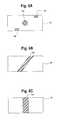
- FIG. 1Ais a side view of a printable label embodiment of this invention.
- FIG. 1Bis a side view of a decoupler embodiment of this invention.
- FIG. 2is an assembled decoupled EM tag embodiment of this invention prepared by combining the FIG. 1A and FIG. 1B pieces;
- FIG. 3is loop antenna embodiment
- FIG. 4is a cross section of an item housing including an integral decoupler
- FIGS. 5A and 5Bare side views of several more decoupler embodiments useful in the present invention.
- FIGS. 6A-6Care overhead views of decoupler embodiments of this invention showing the location of gap 235 ;
- FIGS. 7A , 7 B and 7 Cshow embodiments of a printable layer decoupler and decoupled EM tag respectively;
- FIG. 8is an embodiment of a printable label of this invention that can be associated with different decoupler configurations to form different decoupled EM tag configurations;
- FIGS. 9A , 9 B and 9 Care decoupler configurations that can be combined with the printable label of FIG. 8 to form decoupled EM tag configurations;
- FIGS. 10A , 10 B and 10 Care decoupled EM tag configurations made by combining the decouplers of FIG. 9A , 9 B or 9 C with the printable label embodiment shown in FIG. 8 ;
- FIGS. 11A and 11Care deconstructed decoupler and decoupler/label embodiments of the present invention while FIG. 11B is a decoupler made from the deconstructed decoupler shown in FIG. 11A .
- the present inventionrelates to methods of assembly, labeling and programming decoupled EM tags used in the tagging and tracking of items such as assets, manufactured goods, work in progress, documents or any objects where a unique item identification scheme is required.
- the present inventionalso concerns unique parts that are used in the decoupled EM tag assembly methods as well as kits including mixtures of parts that allow for the assembly of a variety of decoupled EM tag configurations.
- the inventionis specific to tags or EM tags, which manipulate electromagnetic radiation (EM) into identification devices such as RF (radio frequency) tags, also known as RFID tags, that use a structure to decouple (i.e. isolate) the tag from surfaces that degrade its read performance, such as metallic surfaces and surfaces of liquid containers.
- the inventionis a decoupled RFID tag that is deployed to the user as two discreet components (1) a decoupler; and (2) a printable label including an EM device.
- the componentscan be supplied as a single deconstructed sheet of material. Deploying the components as two parts or as a single deconstructed sheet allows the end user to apply a unique identifier to the printable label by printing, then encoding the portion of the tag that includes the EM device to be encoded and the tag labeled using standard printing and encoding technology in no particular order. The printable label and decoupler are then assembled to form a fully functional decoupled EM tag.
- FIGS. 1A and 1Bare embodiments of two possible parts of this invention that can be used—on site—to construct decoupled EM tags in accordance with this invention.
- the device first partis a printable label 10 having a printable layer 12 , a programmable device 14 , an antenna 16 associated with the programmable device 14 , an adhesive layer 17 and an optional backing layer 18 .
- the printable labelmay optionally include one or more alignment features 20 .
- FIG. 1Bis an embodiment of the second part—a decoupler 30 .
- Decoupler 30 shown in FIG. 1Bincludes a layer of metal forming a first conducting side wall 32 spaced apart from and parallel to a second layer of metal forming a second conducting side wall 34 .
- Conducting side walls 32 and 34define a sub-wavelength cavity, one end of which is closed by a conducting end wall or base portion 38 .
- the combination of side walls 32 and 34 and end wall 38forms a cavity that encloses a dielectric material 36 which may be air or may be one or more layers of dielectric material such as PET.
- One or both of the first and second conducting side walls 32 and 34may be continuous with the conducting base portion 38 .
- Decoupler 30may optionally include one or more alignment features 40 that are complementary to alignment features 20 associated with printable label 10 .
- the thickness of conducting side walls 32 and 34 , conducting end wall 38 and dielectric material 36may be small.
- the thicknessmay be much less than the operating wavelength.
- the total thickness of certain embodimentsmay be less than ⁇ /10, or ⁇ /300 or ⁇ /1000.
- the thicknessmay be 1 mm or less, 2 mm or less, or 500 ⁇ m or less, or 100 ⁇ m or less.
- Embodiments of the present inventioncan therefore be thinner and lighter compared to foam spacers or known tuned antenna arrangements. Further, selection of appropriate materials and thicknesses can allow such a device to be flexible, enabling it to be applied to non-planar or curved surfaces.
- Decoupler 30is designed to decouple radiation at a particular frequency. It is convenient to consider a simplistic model of the functionality of the decoupler, in which RF waves are coupled into the cavity and propagate along inside it until they reach either a closed end e.g. metal wall, or an open end. A proportion of the wave is reflected at the end (whether the end is open or closed) and travels back along inside the cavity.
- the decouplermay be a convoluted structure, as shown in FIG. 5B , that is folded upon itself to create, in effect, a smaller footprint without sacrificing performance.
- FIGS. 1B , 4 , 5 A- 5 B, 6 A- 6 C, 7 B and 9 A- 9 CSome useful decouplers are also described in U.S. patent application Ser. Nos. 11/474,082; 11/763,570; 12/519,657; and 12/519,109, the specifications each of which are incorporated herein by reference.
- printable label 10should be of a size including a width, length and thickness sufficient to allow to be fed into a standard printer and/or an RFID capable label printer and/or label printer/programmer.
- RFID printers and/or tag programmersinclude, but are not limited to Zebra S4M, ZM400 RZ400 and R4PT; Sato GL408 and GL408e; and Vionix T4M and SL4M.
- Printable label 10is preferably sized so that its dimensions are essentially the same as the planar surface dimensions of decoupler 30 . That way, the decoupler surface is also protected by printable label 10 .
- printable labelwill have a length ranging from about 3 mm to about 150 mm and a width ranging from about 3 mm to about 150 mm with more preferred dimensions ranging from a length of 3 mm to 30 mm and a width of from 3 mm to 15.24 mm.
- the top surface of printable label 10is a printable layer 12 .
- the printable layerwill typically include a layer of paper or printable polymeric material.
- antenna 16 and programmable device 14are typically associated with the printable layer 12 using a layer 11 of adhesive or curable polymer material.
- Printable layer 12can be transparent or opaque. Moreover, the printable layer may be preprinted with some or all required printed subject matter. If the selected printable layer 12 is a polymer film, then useful polymer films may include, for example, be polyester films, polyvinyl chloride films, polyolefin films (poly-propylene, polyethylene), polycarbonate films, polystyrene films, polyamide films or cellulose acetate films. The printable layer or film will have a thickness of preferably from 8 microns to about 200 microns.
- adhesive or polymer material layer 11is applied to the inside surface 13 of printable layer 12 .
- Antenna 16 and programmable device 14are attached to the adhesive material and the adhesive material is cured.
- adhesive layer 17is applied to the cured layer 11 containing antenna 14 and programmable device 16 and optional backing layer 18 is applied to adhesive layer 17 to cover and protect it.
- Antenna 16will typically be made from an electrically conductive material and adhesively applied to the bottom of printable layer 12 or to one or both sides of an optional support or carrier film layer 15 which is preferably made of plastic.
- Antenna 16will include antenna contacts which are associated with programmable device 14 .
- Antenna 14will typically have a thickness of from 1 to about 50 microns or more.
- the programmable device 14is likewise fastened to the bottom of printable layer 12 or to optional carrier film layer 15 .
- Programmable device 14will typically include first and second electrical contacts to facilitate an electrical connection between programmable device 14 and antenna 16 .
- An electrically conductive adhesivecan be used to facilitate the electrical connection.
- Antenna 14 and programmable device 16can be arranged on the same side of the optional carrier film layer 15 . However the orientation of antenna 16 with respect to programmable device 14 can change depending upon many factors including the dimension requirements for printable label 10 , the size of the components of printable label 10 and so forth.
- the exposed surface 21 of the printable layer 12may be a heat-sensitive recording layer.
- the printable layerwill include dye precursor compound(s) which, when exposed to heat, reacts with a suitable partner compound to form a color.
- the printable layeris designed as an ink-receiving recording layer for printing by means of the inkjet process.
- Adhesive layer 17can be formed from commercially customary acrylic adhesives or customary laminating adhesives, especially if the cover layer is to be fastened permanently to the carrier film.
- the cover layer usedis paper or card or a polymer film, in order to enable the printable RFID transponders to be used directly as identification cards, access authorization cards or tags.
- the basis weight of the paper/board for the cover layeris selected in accordance with the card rigidity required for the intended use.
- a self-sticking or pressure sensitive adhesiveis used to form the adhesive layer 17 .
- suitable pressure-sensitive adhesives for forming a pressure-sensitive adhesive layerare pressure-sensitively adhering aqueous dispersions based on acrylic acid, acrylate and copolymers thereof with vinyl acetate, acrylonitrile, diacetone acrylamide and/or crosslinked comonomers (e.g.
- divinylbenzene or ethylene dimethacrylatewith and without modifying resin dispersions (hydrocarbon resins, alkylphenol resins, terpene-phenol resins, betapinene resins, rosins, methylstyrene-vinyltoluene resins), acrylate pressure-sensitive adhesives in solution in organic solvents with, for example, rosin triglyceride resins or hydrogenated rosins as tackifier component, acrylates derivatized by copolymerization with bifunctional monomers, such as divinylbenzene or ethylene dimethacrylate, or by Copolymerisation with UV photoinitiators (e.g.
- tackifier resinse.g. aliphatic olefin resins, rosins or terpene-phenol resins or polyaromatic compounds, or petroleum-spirit-dissolved pressure-sensitive adhesives based on natural rubber, with coumarone-indene resins, rosins or hydrocarbon resins (e.g. polyterpenes or poly-beta-pinene) as tackifiers.
- adhesive layer 17is optionally covered with backing layer 18 in order to protect the adhesive layer before it is applied to the decoupler.
- Backing layer 18may be selected from any layer or sheet material that is designed to be detachable from an adhesive layer. Such backing layers will typically have at least one surface finished in such a way that on contact with the adhesive a connection is formed which, however, can be broken again without adversely affecting the adhesion of the adhesive layer.
- suitable backing layers 18include those having a surface layer including optional release agents such as polymers based on cellulose acetate, (meth)acrylates, acrylonitrile, vinyl chloride, vinyl ethers or copolymers thereof with, for example, maleic anhydride or modified with aldehyde resins or imine resins; waxes based on polyethyleneamides or polyamides and/or mixtures thereof with polymers based on nitrocellulose, polystyrene or vinyl chloride-vinyl acetate copolymers; polyvinyl esters with long-chain alcohols; chromium stearates and derivatives based thereon; and crosslinked polyorganosiloxanes, alone or in a mixture with vinyl ethers and/or maleic anhydride polymers.
- optional release agentssuch as polymers based on cellulose acetate, (meth)acrylates, acrylonitrile, vinyl chloride, vinyl ethers or copolymers thereof with, for example, maleic anhydride or modified
- the printable sheet, the interlayer and the adhesive layercan be applied to the carrier film by customary techniques known for this purpose.
- pressure-sensitive adhesive layersand especially when these are to be applied from organic solvents, it is preferred to form a pressure-sensitive adhesive layer on the cover layer which has been provided with a release effect (adhesive property) and then to bring the polymer carrier film with the RFID transponders formed thereon into contact with the pressure-sensitive adhesive layer.
- at least one pre-prepared parting lineas an intended separation point between the labels transversely to the running direction of the strip, in order to facilitate the separation of printed or unprinted labels from the strip.
- antenna 16 and programmable device 14are placed in a curable polymer material and the curable polymer is then cured to form a sheet precursor. Thereafter, a printable layer 12 is applied to one surface of the sheet precursor and an adhesive layer 17 and optional backing sheet 18 are applied to the opposite surface of the sheet precursor to form printable label 10 .
- a plurality of printable labels 10are applied to a single backing layer 18 to form a sheet product that includes a plurality of printable labels 10 .
- the sheetcan take the form of a single sheet of paper, it can take the form of a strip of paper that is then rolled into or roll, and it can take on any other form that can be continuously or intermittently fed into a printer/tag programming device.
- the antenna 14 associated with printable label 10may be any antenna known in the art to be useful with decoupled EM tags.
- the RFID tags assembled in the present inventionmay use an RF tag which only has a small antenna.
- the decouplercouples radiation into its dielectric core and produces a high electric field at the open end of the cavity, a tag located in this region will be operating in an area of high field and will not require a large tuned antenna.
- the decoupler of the present inventioncan be used with a so called low Q tag.
- FIG. 3shows an example of a low Q tag, which has a small loop 70 which connects to a programmable device 14 ′ such as a chip.
- the loopmay be approximately 20 mm in length.
- the low Q tagwill not function in free space unless the interrogating wavelength corresponds to the antenna's perimeter (e.g. 6 GHz operation for a 5 cm loop), and hence will not operate at standard UHF frequencies (e.g. 866 MHz) unless the reader is located within 1 or 2 mm of the chip, because the antenna 14 ′ is inefficient at coupling to incident UHF radiation.
- the low Q tagwhich may be only slightly larger than the chip itself, may be placed on any decoupler according to the invention.
- the small loop sectionmay be replaced by short ‘arms’ that extend outwards or partially wrap around a spacer, since even two short ‘stubs’ of metal are sufficient to help tune to the proper frequency and thereby couple power into the chip if combined with a correctly designed decoupler.
- Reduction in the antenna sizeallows for a more compact RF ID system without the need to wrap existing antennas around the body of the decoupler.
- a yet further advantageis reduced materials for the RF ID manufacture process.
- the programmable device 14may be any programmable device that can be associated with a decoupled EM or RFID tag in order to facilitate the functioning of the tag. It will be appreciated that a variety of programmable devices, such as RFID chips may be used in the present invention. Suitable RFID chips include Philips HSL chip, available from Philips Electronics, and the EM Marin EM4222, available from EM Microelectronic-Marin SA, as well as RFID chips available from Impnj (the Monza chip), Alien Technology (Higgs chip), NXP (the X-rag chip), Texas Instruments, Samsung and Hitachi.
- Each printable label 10may include one or more optional alignment features 20 .
- Alignment feature 20may be any feature(s) that allows printable label 10 to be properly aligned with decoupler 30 such that the resulting decoupled RFID tag is operable.
- Alignment features 20 and 40may, for example, be a combination of grooves, alignment holes, alignment marks, recessed surfaces, raised edges and so forth that facilitate correct alignment of the two parts to form a decoupled EM tag.
- a jig or other similar devicemay be used during the attachment process to speed assembly and insure correct placement.
- the programmable device 16 in printable label 10must be located at a portion of the decoupler top surface that is not covered by a conducting side wall 32 or 34 .
- the programmable device 14 of printable label 10 in FIG. 1Acan be placed over gap 37 of decoupler 30 of FIG. 1B to form the decoupled EM tag shown in FIG. 1C .
- the EM tags of this inventionare still operable if programmable device 14 straddles end 33 of second conducting side wall 34 or even if the programmable device is placed at a minus location on the tuning plane.
- Alignment feature 20may or may not be complementary with alignment feature 40 of decoupler 30 .
- alignment feature 20may be one or more depressions or one or more raised tabs that are complementary to tabs or depressions on the surface of decoupler 30 to which printable label 10 is adhered.
- alignment feature 40may be one or more tabs 45 complementary to indentations in printable label 10
- alignment feature 20may be a hole that passes completely through label 10 that is aligned with a complementary mark on decoupler 30 .
- the decoupled EM tags of this inventioncan be prepared using two parts by the following steps.
- a first stepis to direct printable label 10 into a printer or some other device.
- One purpose of the printing stepis to apply an optional unique identifier such as a one or two dimensional barcode, an inventory number, or some other identifier to the surface of printable label 10 .
- the programmable device 14 associated with printable label 10is also programmed during or immediately after the assembly process.
- the printed and optionally programmed printable label 10is manipulated to expose adhesive layer 17 .
- This manipulationcan include removing the optional backing layer 18 from the label to expose the pre-applied adhesive layer 17 or it can include applying an adhesive material layer to the label bottom surface or decoupler top surface.
- the adhesive layer 17is placed against decoupler top surface 43 in order to form a decoupled EM tag such as that shown in FIG. 1C .
- the assembly processcan be a fully manual process, optionally facilitated by placement of alignment marks on the separate components; partially automated by the use of a jig or similar device to insure that the pieces are assembled to tolerance; or fully automated, either as part of the printing and encoding process, or as a separate device, the result of which combines the two pieces to form a functional decoupled EM tag.
- FIG. 2An embodiment of a decoupled EM tag 100 of this invention is shown in FIG. 2 where decoupled EM tag is associated with the surface 102 of an item.
- decoupler 30 or decoupled EM tag 100will be attached to an item via adhesive layer 27 associated with the first conductive side wall 32 .
- EM tag 100includes a printed top surface 101 .
- EM tag 100includes an antenna 16 and programmed device 14 ′ where the programmed device 14 ′ lies at least partially to totally over a portion of the decoupler top surface 19 that is not covered with the conducting side wall 34 material.
- Other decoupled EM tag embodimentsthat fall within the scope of this invention are discussed below.
- the EM tags of this inventionare generally associated with an item.
- the “item”refers to any tangible creation or construction which is known now to be usefully tagged with an EM tag and any future item that becomes know to be usefully tagged with an EM tag.
- Some limited examples of itemsinclude consumer items such as computers, televisions, cameras, appliances. automobiles and the like, industrial items such as parts, machines, tools and the like, items that are moving such as robots, trucks, automobiles, and packages, boxes, crates etc. . . . that are used to store and/or ship items. While the numbers of items that EM tags can be applied to is near infinite, it is preferred that the decoupled EM tags of this invention are applied to items having metal surfaces or that hold liquids as such items are able to be effectively EM tagged with coupled EM tags.
- a decoupler 130can be pre-manufactured into an item.
- a decouplercan be formed into a computer case or into a telephone switch.
- FIG. 4is a cross section of a case or housing 150 for an item.
- Housing 150includes an outside metal skin 152 that forms second conducting side wall portion 134 of decoupler 130 .
- conductive base portion 138which electrically unites essentially parallel first and second conducting side walls 132 and 134 .
- the combination of conducting side walls 132 and 134 and base portion 138defines a sub-wavelength cavity 135 that encloses a dielectric material 136 which may be air or may be one or more dielectric materials.
- a decouplerWhen a decoupler is pre-manufactured into an item, the end user has a choice of whether or not to attach a printed and programmed printable sheet 10 to the housing to form an EM tag. Incorporating the decoupler into the item also eliminates the need for the end user to purchase a separate decoupler to form a decoupled EM tag.
- the first decoupler configurationis shown in FIG. 1B and described above.
- An alternative decoupler configuration 30 ′is shown in FIG. 5A .
- This alternative decoupler structureincludes a first conducting side wall 232 and a second conducting side wall 234 oriented essentially parallel to one another and spaced apart from one another by dielectric material layer 236 .
- first conducting side wall 232 and second conducting side wall 234are not electrically connected.
- the conductive material layer on the decoupler top surfaceshould include a gap 235 that exposes the underlying dielectric material. In the embodiment shown in FIG.
- the gap 19is located at an edge of the decoupler and is formed as a result of the decoupler first side wall and second side wall having unequal lengths.
- gap 235may be formed by placing a hole, a space or so forth in the second conducting side wall 234 and as shown from above in FIGS. 6A-6C .
- the decoupler second conducting side wall 34can be associated with printable sheet 10 and thereafter applied to a decoupler embodiment to form a decoupled EM tag.
- FIGS. 7A , 7 B and 7 Cshow a printable layer embodiment, decoupler and decoupled EM tag respectively made in accordance with this alternative embodiment.
- FIG. 7Ais a printable sheet 10 ′ having a printable layer 12 , a programmable device 14 , an antenna 16 , and an adhesive layer 17 . Interposed between the adhesive layer 17 and the antenna 16 and programmable device 14 is a conducting side wall layer 60 .
- the printable label 10 ′ shown in FIG. 7Ais applied to decoupler 30 ′′ of FIG. 7B .
- Decoupler 30 ′′includes a first conducting side wall 32 , a conducting end wall 38 and a dielectric layer 36 .
- label 10 ′is adhesively associated with decoupler 30 ′′, the result is the decoupled EM tag shown in FIG. 7C having a decoupler that now includes a second conducting side wall 34 .
- FIG. 8is a printable label embodiment 200 that can be used in conjunction with two or more decoupler configurations to form two or more decoupled EM tag configurations.
- Printable label 200includes a printable layer 12 , a programmable device 14 , an antenna 16 , and an adhesive layer 17 . Interposed between the adhesive layer 17 and the antenna 16 and programmable device 14 is a conducting side wall layer 60 .
- printable label 200may or may not include an indentation(s) 205 that runs along the length of the label to assist in applying a fold to the label.
- FIGS. 9A , 9 B and 9 Care decoupler embodiments 300 , 301 and 302 .
- Decoupler embodiments 300 and 301both include a first conducting side wall 32 and a dielectric layer 36 .
- One difference between decoupler 300 and decouplers 301 and 302is that decoupler 300 has a length that is essentially equal to the length of printable label 200 while printable label 200 is longer than decouplers 301 and 302 .
- FIGS. 10A , 10 B and 10 Cshow decoupled RF tags 310 , 311 and 312 formed by applying printable label 200 to the top surface of each of decouplers 300 , 301 and 301 .
- the decoupled EM tag of FIG. 9Ais essentially identical to the decoupled EM tag shown in FIG. 5 that has no conducting end wall.
- Decoupled EM tags 311 and 312are more like the decoupled EM tag shown in FIG. 2 except that printable label 200 is folded at one edge of decoupler 301 to form a cavity defined by first and second conductive side walls 32 and 34 and end wall 36 .
- Decoupled EM tag 312includes no integral first conductive side wall.
- decoupler 302is associated with a metal surface 315 which effectively becomes the first conductive side wall.
- Printable label 200is then folded at one edge of decoupler 302 to form, in combination with metal surface 315 , a cavity defined by metal surface 315 , second conductive side walls 34 and end wall 36 .
- the same printable labelcan be combined with decouplers having different configurations to form a variety of decoupled EM tags.
- FIGS. 11A-11CStill another embodiment of this invention is shown in FIGS. 11A-11C .
- FIG. 11Ais a deconstructed, very thin sheet useful for fabricating a decoupler portion of an EM tag.
- the deconstructed decouplerincludes at least a partial adhesive layer 275 overlayed by a conductive material layer 276 which in turn is overlayed by a dielectric material layer 277 .
- a second thin adhesive layer 278On top of the dielectric material layer 277 is a second thin adhesive layer 278 .
- the conductive material layer 276 shown in FIG. 11Adoes not extend to the edge of the sheet. However, in certain embodiments, the conductive material layer can extend to the edge of the sheet depending upon the type of decoupler that will be constructed from the sheet.
- the sheetincludes folding sites 279 and 279 ′.
- the decoupler shown in FIG. 11Bis fabricated by upwardly folding the sheet at fold 279 ′ until the adhesive material layer 278 associated with the folded portion 280 contacts the stationary dielectric surface 283 such that the conductive material layer portion of the folded portion is essentially parallel to the conductive material layer portion of the stationary portion.
- the sheet shown in FIG. 11Ais folded upwardly at fold 279 until the adhesive material layer 278 associated with folded portion 281 abuts the now upwardly facing surface 282 of the conductive material layer portion associated with folded portion 280 .
- the conductive material layer portion associated with folded portion 281will be essentially parallel to the conductive material layer portion associated with folded portion 280 .
- the resulting decoupleris shown in FIG. 11B .
- FIG. 11Cshows the deconstructed decoupler of FIG. 11A further including an integral printable sheet 10 .
- the printable sheet 10includes a printable surface, a programmable device 14 and an antenna 16 .
- the combinationforms a deconstructed printable and programmable EM tag that, after printing, programming and folding as described above forms a decoupled EM tag as shown essentially in FIG. 10B .
- the embodiments of this inventionall use or include printable labels.
- the printable labelsare printed and programmed as discussed above by loading a sheet including one or more printable labels 10 as a single or continuous stream of labels preferably either in a roll or fanfoled into a printer and programmer.
- the userthen inputs program settings into the printer/programmer to set such variables as the number of labels to be printed, what is to be printed on the labels and so forth.
- the printerthen forms an image on the surface of the printable layer of printable label 10 and the programmable device is automatically programmed as it enters and/or exits the printing/programming device.
- the printable labels 10 and decouplers 30can be provided separately or they may be sold in kits. As noted above, the decoupler can be manufactured into the item being tagged. Alternatively, kits including the same type or a variety decoupler sizes and types can be supplied to the end user along with corresponding multiple label sizes. The user can, on-demand, select an appropriate decoupler size and then select the appropriate label for the decoupler before printing, programming and applying the label to the decoupler to form a decoupled EM tag.
Landscapes
- Engineering & Computer Science (AREA)
- Physics & Mathematics (AREA)
- Microelectronics & Electronic Packaging (AREA)
- Computer Hardware Design (AREA)
- General Physics & Mathematics (AREA)
- Theoretical Computer Science (AREA)
- Electromagnetism (AREA)
- Making Paper Articles (AREA)
- Details Of Aerials (AREA)
Abstract
Description
Claims (14)
Priority Applications (3)
| Application Number | Priority Date | Filing Date | Title |
|---|---|---|---|
| US12/544,766US8794533B2 (en) | 2008-08-20 | 2009-08-20 | One and two-part printable EM tags |
| US13/432,291US8636223B2 (en) | 2008-08-20 | 2012-03-28 | One and two-part printable EM tags |
| US14/328,572US20150161499A1 (en) | 2008-08-20 | 2014-07-10 | One and Two-Part Printable EM Tags |
Applications Claiming Priority (2)
| Application Number | Priority Date | Filing Date | Title |
|---|---|---|---|
| US9056408P | 2008-08-20 | 2008-08-20 | |
| US12/544,766US8794533B2 (en) | 2008-08-20 | 2009-08-20 | One and two-part printable EM tags |
Related Child Applications (2)
| Application Number | Title | Priority Date | Filing Date |
|---|---|---|---|
| US13/432,291DivisionUS8636223B2 (en) | 2008-08-20 | 2012-03-28 | One and two-part printable EM tags |
| US14/328,572ContinuationUS20150161499A1 (en) | 2008-08-20 | 2014-07-10 | One and Two-Part Printable EM Tags |
Publications (2)
| Publication Number | Publication Date |
|---|---|
| US20100045025A1 US20100045025A1 (en) | 2010-02-25 |
| US8794533B2true US8794533B2 (en) | 2014-08-05 |
Family
ID=41259811
Family Applications (3)
| Application Number | Title | Priority Date | Filing Date |
|---|---|---|---|
| US12/544,766Active2031-11-27US8794533B2 (en) | 2008-08-20 | 2009-08-20 | One and two-part printable EM tags |
| US13/432,291ActiveUS8636223B2 (en) | 2008-08-20 | 2012-03-28 | One and two-part printable EM tags |
| US14/328,572AbandonedUS20150161499A1 (en) | 2008-08-20 | 2014-07-10 | One and Two-Part Printable EM Tags |
Family Applications After (2)
| Application Number | Title | Priority Date | Filing Date |
|---|---|---|---|
| US13/432,291ActiveUS8636223B2 (en) | 2008-08-20 | 2012-03-28 | One and two-part printable EM tags |
| US14/328,572AbandonedUS20150161499A1 (en) | 2008-08-20 | 2014-07-10 | One and Two-Part Printable EM Tags |
Country Status (2)
| Country | Link |
|---|---|
| US (3) | US8794533B2 (en) |
| WO (1) | WO2010022250A1 (en) |
Cited By (2)
| Publication number | Priority date | Publication date | Assignee | Title |
|---|---|---|---|---|
| US10586144B2 (en) | 2014-09-29 | 2020-03-10 | Avery Dennison Corporation | Tire tracking RFID label |
| US12400100B2 (en) | 2022-11-17 | 2025-08-26 | Hid Global Corp. | On-metal RFID tag |
Families Citing this family (25)
| Publication number | Priority date | Publication date | Assignee | Title |
|---|---|---|---|---|
| WO2007000578A2 (en) | 2005-06-25 | 2007-01-04 | Omni-Id Limited | Electromagnetic radiation decoupler |
| GB0611983D0 (en) | 2006-06-16 | 2006-07-26 | Qinetiq Ltd | Electromagnetic radiation decoupler |
| GB0624915D0 (en)* | 2006-12-14 | 2007-01-24 | Qinetiq Ltd | Switchable radiation decoupling |
| GB0625342D0 (en)* | 2006-12-20 | 2007-01-24 | Qinetiq Ltd | Radiation decoupling |
| US8794533B2 (en) | 2008-08-20 | 2014-08-05 | Omni-Id Cayman Limited | One and two-part printable EM tags |
| US8857724B2 (en) | 2009-03-10 | 2014-10-14 | Wal-Mart Stores, Inc. | Universal RFID tags and methods |
| US8286887B2 (en) | 2009-03-10 | 2012-10-16 | Wal-Mart Stores, Inc. | RFID tag sensors and methods |
| JP2012520517A (en)* | 2009-03-10 | 2012-09-06 | ウォルマート ストアーズ,インコーポレーティッド | Universal RFID tag and manufacturing method |
| JP5170156B2 (en)* | 2010-05-14 | 2013-03-27 | 株式会社村田製作所 | Wireless IC device |
| WO2012115717A2 (en)* | 2011-02-24 | 2012-08-30 | Mcclung Guy L Iii | Nanotag indentification systems and methods |
| JP5777096B2 (en)* | 2011-07-21 | 2015-09-09 | 株式会社スマート | Universal IC tag, its manufacturing method, and communication management system |
| CN103797498B (en)* | 2011-09-12 | 2016-10-12 | 日立化成株式会社 | RFID tags and automatic identification systems |
| US20130313328A1 (en)* | 2012-05-25 | 2013-11-28 | Omni-Id Cayman Limited | Shielded Cavity Backed Slot Decoupled RFID TAGS |
| US9355349B2 (en) | 2013-03-07 | 2016-05-31 | Applied Wireless Identifications Group, Inc. | Long range RFID tag |
| US9400900B2 (en) | 2013-03-14 | 2016-07-26 | Wal-Mart Stores, Inc. | Method and apparatus pertaining to RFID tag-based user assertions |
| US9251488B2 (en) | 2013-04-25 | 2016-02-02 | Wal-Mart Stores, Inc. | Apparatus and method of determining a likelihood of task completion from information relating to the reading of RFID tags |
| US9230145B2 (en) | 2013-04-25 | 2016-01-05 | Wal-Mart Stores, Inc. | Apparatus and method pertaining to conveying information via an RFID transceiver |
| US9773134B2 (en) | 2013-04-26 | 2017-09-26 | Wal-Mart Stores, Inc. | Apparatus and method pertaining to switching RFID transceiver read states |
| EP3147260A4 (en)* | 2014-02-24 | 2017-11-29 | Sekisui Chemical Co., Ltd. | Carbon material, resin composite material, and method for producing said carbon material and resin composite material |
| GB2539133B (en) | 2014-04-02 | 2021-02-10 | Walmart Apollo Llc | Apparatus and method of determining an open status of a container using RFID tag devices |
| CA2970672A1 (en) | 2014-12-31 | 2016-07-07 | Wal-Mart Stores, Inc. | System, apparatus and method for sequencing objects having rfid tags on a moving conveyor |
| US10607131B2 (en)* | 2015-12-08 | 2020-03-31 | Avery Dennison Retail Information Services, Llc | Self adhesive label and RFID inlay |
| FR3055054B1 (en)* | 2016-08-11 | 2019-07-05 | Veronique Meunier | PRINTING MULTILAYER DEVICE WITH ELECTRONIC CHIP AND METHOD OF MANUFACTURING THE SAME |
| US9665821B1 (en)* | 2016-12-19 | 2017-05-30 | Antennasys, Inc. | Long-range surface-insensitive passive RFID tag |
| CN111867231A (en)* | 2019-04-30 | 2020-10-30 | 宏启胜精密电子(秦皇岛)有限公司 | Closed flexible main board and manufacturing method thereof |
Citations (110)
| Publication number | Priority date | Publication date | Assignee | Title |
|---|---|---|---|---|
| US2990547A (en) | 1959-07-28 | 1961-06-27 | Boeing Co | Antenna structure |
| US3065752A (en) | 1959-11-14 | 1962-11-27 | Philips Corp | High frequency therapeutic radiator |
| US4242685A (en) | 1979-04-27 | 1980-12-30 | Ball Corporation | Slotted cavity antenna |
| US4498076A (en) | 1982-05-10 | 1985-02-05 | Lichtblau G J | Resonant tag and deactivator for use in an electronic security system |
| US4714906A (en) | 1984-05-30 | 1987-12-22 | Compagnie D'electronique Et De Piezo-Electricite | Dielectric filter with variable central frequency |
| US4728938A (en) | 1986-01-10 | 1988-03-01 | Checkpoint Systems, Inc. | Security tag deactivation system |
| JPS63151101A (en) | 1986-12-15 | 1988-06-23 | Nec Corp | Micro strip antenna |
| US4835524A (en) | 1987-12-17 | 1989-05-30 | Checkpoint System, Inc. | Deactivatable security tag |
| US4890111A (en) | 1986-10-22 | 1989-12-26 | Eta S.A. Fabriques D'ebauches | Passive transponder |
| EP0512491A1 (en) | 1991-05-06 | 1992-11-11 | Hughes Aircraft Company | Flat cavity RF power divider |
| EP0548851A1 (en) | 1991-12-24 | 1993-06-30 | Knogo Corporation | Stabilized article surveillance responder |
| US5276431A (en) | 1992-04-29 | 1994-01-04 | Checkpoint Systems, Inc. | Security tag for use with article having inherent capacitance |
| US5557279A (en) | 1993-09-28 | 1996-09-17 | Texas Instruments Incorporated | Unitarily-tuned transponder/shield assembly |
| US5565875A (en) | 1992-06-16 | 1996-10-15 | Societe Nationale Industrielle Et Aerospatiale | Thin broadband microstrip antenna |
| US5677698A (en) | 1994-08-18 | 1997-10-14 | Plessey Semiconductors Limited | Slot antenna arrangement for portable personal computers |
| US5682143A (en) | 1994-09-09 | 1997-10-28 | International Business Machines Corporation | Radio frequency identification tag |
| US5949387A (en) | 1997-04-29 | 1999-09-07 | Trw Inc. | Frequency selective surface (FSS) filter for an antenna |
| US5973600A (en) | 1997-09-11 | 1999-10-26 | Precision Dynamics Corporation | Laminated radio frequency identification device |
| US5995048A (en) | 1996-05-31 | 1999-11-30 | Lucent Technologies Inc. | Quarter wave patch antenna |
| US6049278A (en) | 1997-03-24 | 2000-04-11 | Northrop Grumman Corporation | Monitor tag with patch antenna |
| US6072383A (en) | 1998-11-04 | 2000-06-06 | Checkpoint Systems, Inc. | RFID tag having parallel resonant circuit for magnetically decoupling tag from its environment |
| EP1018703A1 (en) | 1999-01-04 | 2000-07-12 | Sihl GmbH | Laminated, multilayer labelweb comprising RFID-transponders |
| US6118379A (en) | 1997-12-31 | 2000-09-12 | Intermec Ip Corp. | Radio frequency identification transponder having a spiral antenna |
| US6121880A (en) | 1999-05-27 | 2000-09-19 | Intermec Ip Corp. | Sticker transponder for use on glass surface |
| US6130612A (en) | 1997-01-05 | 2000-10-10 | Intermec Ip Corp. | Antenna for RF tag with a magnetoelastic resonant core |
| US6147605A (en) | 1998-09-11 | 2000-11-14 | Motorola, Inc. | Method and apparatus for an optimized circuit for an electrostatic radio frequency identification tag |
| EP1055943A2 (en) | 1999-05-24 | 2000-11-29 | Hitachi, Ltd. | A wireless tag, its manufacturing and its layout |
| US6172608B1 (en) | 1996-06-19 | 2001-01-09 | Integrated Silicon Design Pty. Ltd. | Enhanced range transponder system |
| US6208235B1 (en) | 1997-03-24 | 2001-03-27 | Checkpoint Systems, Inc. | Apparatus for magnetically decoupling an RFID tag |
| US6229444B1 (en) | 1997-09-12 | 2001-05-08 | Mitsubishi Materials Corporation | Theftproof tag |
| US6239762B1 (en) | 2000-02-02 | 2001-05-29 | Lockheed Martin Corporation | Interleaved crossed-slot and patch array antenna for dual-frequency and dual polarization, with multilayer transmission-line feed network |
| US6265977B1 (en) | 1998-09-11 | 2001-07-24 | Motorola, Inc. | Radio frequency identification tag apparatus and related method |
| US6271793B1 (en) | 1999-11-05 | 2001-08-07 | International Business Machines Corporation | Radio frequency (RF) transponder (Tag) with composite antenna |
| US6285342B1 (en) | 1998-10-30 | 2001-09-04 | Intermec Ip Corp. | Radio frequency tag with miniaturized resonant antenna |
| US6307520B1 (en) | 2000-07-25 | 2001-10-23 | International Business Machines Corporation | Boxed-in slot antenna with space-saving configuration |
| US20010036217A1 (en) | 2000-03-17 | 2001-11-01 | Kopf David E. | Reconfigurable resonant cavity with frequency-selective surfaces and shorting posts |
| US6339406B1 (en) | 1997-11-25 | 2002-01-15 | Sony International (Europe) Gmbh | Circular polarized planar printed antenna concept with shaped radiation pattern |
| US6366260B1 (en) | 1998-11-02 | 2002-04-02 | Intermec Ip Corp. | RFID tag employing hollowed monopole antenna |
| US20020130817A1 (en) | 2001-03-16 | 2002-09-19 | Forster Ian J. | Communicating with stackable objects using an antenna array |
| US6456228B1 (en) | 1999-02-09 | 2002-09-24 | Magnus Granhed | Encapsulated antenna in passive transponders |
| US20020167500A1 (en) | 1998-09-11 | 2002-11-14 | Visible Techknowledgy, Llc | Smart electronic label employing electronic ink |
| US6483481B1 (en) | 2000-11-14 | 2002-11-19 | Hrl Laboratories, Llc | Textured surface having high electromagnetic impedance in multiple frequency bands |
| US20020170969A1 (en) | 2001-05-16 | 2002-11-21 | Raj Bridgelall | Range extension for RFID hand-held mobile computers |
| US20020175873A1 (en) | 2000-07-18 | 2002-11-28 | King Patrick F. | Grounded antenna for a wireless communication device and method |
| US20020177408A1 (en) | 2000-03-25 | 2002-11-28 | Forster Ian J. | Multiple feed point slot antenna |
| US6507320B2 (en) | 2000-04-12 | 2003-01-14 | Raytheon Company | Cross slot antenna |
| US6509880B2 (en) | 1998-10-23 | 2003-01-21 | Emag Technologies, Inc. | Integrated planar antenna printed on a compact dielectric slab having an effective dielectric constant |
| EP1280231A1 (en) | 2001-07-26 | 2003-01-29 | RF-Link Systems Inc., | A diamond-shaped loop antenna for a wireless I/O device |
| US6516182B1 (en) | 1998-12-21 | 2003-02-04 | Microchip Technology Incorporated | High gain input stage for a radio frequency identification (RFID) transponder and method therefor |
| US6552696B1 (en) | 2000-03-29 | 2003-04-22 | Hrl Laboratories, Llc | Electronically tunable reflector |
| US20030112192A1 (en) | 2000-07-18 | 2003-06-19 | King Patrick F. | Wireless communication device and method |
| US20030197613A1 (en) | 2002-04-22 | 2003-10-23 | David Hernandez | Power source system for RF location/identification tags |
| US6642898B2 (en) | 2001-05-15 | 2003-11-04 | Raytheon Company | Fractal cross slot antenna |
| US6646618B2 (en) | 2001-04-10 | 2003-11-11 | Hrl Laboratories, Llc | Low-profile slot antenna for vehicular communications and methods of making and designing same |
| US20040020036A1 (en) | 2002-08-02 | 2004-02-05 | Matrics, Inc. | Method and apparatus for high volume assembly of radio frequency identification tags |
| JP2004054337A (en) | 2002-07-16 | 2004-02-19 | Oji Paper Co Ltd | IC chip package |
| US20040111338A1 (en) | 1997-11-21 | 2004-06-10 | Matrics, Inc. | System and method for electronic inventory |
| JP2004164055A (en) | 2002-11-11 | 2004-06-10 | Yokowo Co Ltd | Microwave tag system |
| US20040201522A1 (en) | 2003-04-10 | 2004-10-14 | Housing Technology, Inc. | RFID tag using a surface insensitive antenna structure |
| US6812893B2 (en) | 2002-04-10 | 2004-11-02 | Northrop Grumman Corporation | Horizontally polarized endfire array |
| US6816380B2 (en) | 2001-05-31 | 2004-11-09 | Alien Technology Corporation | Electronic devices with small functional elements supported on a carrier |
| US6825754B1 (en) | 2000-09-11 | 2004-11-30 | Motorola, Inc. | Radio frequency identification device for increasing tag activation distance and method thereof |
| US20050012616A1 (en) | 2003-07-07 | 2005-01-20 | Forster Ian J. | RFID device with changeable characteristics |
| US20050030201A1 (en) | 2003-04-21 | 2005-02-10 | Raj Bridgelall | Method for optimizing the design and implementation of RFID tags |
| JP2005094360A (en) | 2003-09-17 | 2005-04-07 | Kyocera Corp | ANTENNA DEVICE AND WIRELESS COMMUNICATION DEVICE |
| US20050092845A1 (en) | 2003-11-03 | 2005-05-05 | Forster Ian J. | Self-compensating antennas for substrates having differing dielectric constant values |
| US20050107092A1 (en) | 2003-11-19 | 2005-05-19 | Hal Charych | System and method for tracking data related to containers using RF technology |
| EP1533867A1 (en) | 2003-11-18 | 2005-05-25 | Alps Electric Co., Ltd. | Circular polarization slot antenna apparatus capable of being easily miniaturized |
| EP1538546A2 (en) | 2003-12-05 | 2005-06-08 | HID Corporation | Low voltage signal stripping circuit for an RFID reader |
| US6911952B2 (en) | 2003-04-08 | 2005-06-28 | General Motors Corporation | Crossed-slot antenna for mobile satellite and terrestrial radio reception |
| EP1548639A1 (en) | 2003-12-25 | 2005-06-29 | Hitachi, Ltd. | Wireless IC tag, and method and apparatus for manufacturing the same |
| EP1548629A1 (en) | 2003-12-26 | 2005-06-29 | Dwango Co., Ltd. | Messenger service system and control method thereof, and messenger server and control program thereof |
| JP2005191705A (en) | 2003-12-24 | 2005-07-14 | Sharp Corp | Wireless tag and RFID system using the same |
| US20050151699A1 (en) | 2004-01-12 | 2005-07-14 | Symbol Technologies, Inc. | Method and system for manufacturing radio frequency identification tag antennas |
| US6944424B2 (en) | 2001-07-23 | 2005-09-13 | Intermec Ip Corp. | RFID tag having combined battery and passive power source |
| US20050200539A1 (en) | 2004-03-11 | 2005-09-15 | Forster Ian J. | RFID device with patterned antenna, and method of making |
| US6946995B2 (en) | 2002-11-29 | 2005-09-20 | Electronics And Telecommunications Research Institute | Microstrip patch antenna and array antenna using superstrate |
| JP2005271090A (en) | 2004-03-23 | 2005-10-06 | Toshiyuki Tani | Staple with wireless chip |
| JP2005303528A (en) | 2004-04-08 | 2005-10-27 | Hidekazu Ogawa | Radio wave polarization conversion resonance reflector, radio wave polarization conversion resonance reflecting apparatus, radio communication system, metal-adaptive radio ic tag, article and rfid system |
| US20060028344A1 (en) | 2003-04-25 | 2006-02-09 | Forster Ian J | Extended range RFID system |
| US20060033609A1 (en) | 2000-06-07 | 2006-02-16 | Raj Bridgelall | Wireless locating and tracking systems |
| US20060043198A1 (en) | 2004-09-01 | 2006-03-02 | Forster Ian J | RFID device with combined reactive coupler |
| US20060049947A1 (en) | 2004-09-09 | 2006-03-09 | Forster Ian J | RFID tags with EAS deactivation ability |
| US20060055542A1 (en) | 2004-09-13 | 2006-03-16 | Forster Ian J | RFID device with content insensitivity and position insensitivity |
| US20060086808A1 (en) | 2004-09-29 | 2006-04-27 | Checkpoint Systems, Inc. | Method and system for tracking containers having metallic portions, covers for containers having metallic portions, tags for use with container having metallic portions and methods of calibrating such tags |
| JP2006157905A (en) | 2004-11-25 | 2006-06-15 | Sontec Co Ltd | Radio frequency identification system |
| US20060131377A1 (en)* | 2004-12-17 | 2006-06-22 | Intermec Ip Corp. | Stand-alone proxy RFID read/write unit for print label encoding |
| US20060145927A1 (en) | 2004-12-08 | 2006-07-06 | Won-Kyu Choi | PIFA and RFID tag using the same |
| US7075437B2 (en) | 2003-01-13 | 2006-07-11 | Symbol Technologies, Inc. | RFID relay device and methods for relaying and RFID signal |
| US20060208897A1 (en)* | 2005-03-04 | 2006-09-21 | Chiu Lihu M | Capacitive RFID tag encoder |
| US20060220869A1 (en) | 2005-03-15 | 2006-10-05 | Intermec Ip Corp. | Tunable RFID tag for global applications |
| US20060220866A1 (en) | 2005-03-29 | 2006-10-05 | Dixon Paul F | RFID tags having improved read range |
| US20060250252A1 (en)* | 2003-10-24 | 2006-11-09 | Takuya Nagai | RFID Tag Information Communicating Device, Cartridge For RFID Tag Information Communicating Device, And RFID Circuit Element Processing System |
| JP2006311239A (en) | 2005-04-28 | 2006-11-09 | Tomozo Ota | Wireless IC tag device and RFID system |
| US20060261950A1 (en) | 2005-03-29 | 2006-11-23 | Symbol Technologies, Inc. | Smart radio frequency identification (RFID) items |
| US20070007342A1 (en) | 2005-07-08 | 2007-01-11 | Cleeves James M | Methods for manufacturing RFID tags and structures formed therefrom |
| GB2428939A (en) | 2005-06-25 | 2007-02-07 | Qinetiq Ltd | Electromagnetic radiation decoupler for an RF tag |
| US7212127B2 (en) | 2004-12-20 | 2007-05-01 | Avery Dennison Corp. | RFID tag and label |
| US20070096852A1 (en)* | 2005-06-25 | 2007-05-03 | Qinetiq Limited | Electromagnetic radiation decoupler |
| US7225992B2 (en) | 2003-02-13 | 2007-06-05 | Avery Dennison Corporation | RFID device tester and method |
| US20070158436A1 (en)* | 2004-01-30 | 2007-07-12 | Hiromitsu Ichikawa | Rfid-incorporating bar code label, tire and management method thereof |
| US7298343B2 (en) | 2003-11-04 | 2007-11-20 | Avery Dennison Corporation | RFID tag with enhanced readability |
| US20070268322A1 (en)* | 2004-10-25 | 2007-11-22 | Toshiaki Kyoi | Printer |
| US20070285907A1 (en) | 2003-08-28 | 2007-12-13 | Kyocera Corporation | Wiring Board and Semiconductor Device |
| US20070290941A1 (en)* | 2006-06-16 | 2007-12-20 | Qinetiq Limited | Electromagnetic Enhancement and Decoupling |
| US7315248B2 (en) | 2005-05-13 | 2008-01-01 | 3M Innovative Properties Company | Radio frequency identification tags for use on metal or other conductive objects |
| US20080129625A1 (en) | 2004-07-13 | 2008-06-05 | Bengt Inge Svensson | Low Profile Antenna |
| US20080164326A1 (en)* | 2007-01-04 | 2008-07-10 | Lintec Corporation | Connecting Part For Mounting IC Chip, Antenna Circuit, IC Inlet, IC Tag and Method of Adjusting Capacitance |
| US20100230497A1 (en) | 2006-12-20 | 2010-09-16 | Omni-Id Limited | Radiation Enhancement and Decoupling |
| US20110037541A1 (en) | 2006-12-14 | 2011-02-17 | Omni-Id Limited | Switchable Radiation Enhancement and Decoupling |
Family Cites Families (3)
| Publication number | Priority date | Publication date | Assignee | Title |
|---|---|---|---|---|
| DE602005021513D1 (en)* | 2004-08-26 | 2010-07-08 | Nxp Bv | RFID LABEL WITH FOLDED DIPOL |
| US20080055045A1 (en)* | 2006-08-31 | 2008-03-06 | 3M Innovative Properties Company | Rfid tag including a three-dimensional antenna |
| US8794533B2 (en) | 2008-08-20 | 2014-08-05 | Omni-Id Cayman Limited | One and two-part printable EM tags |
- 2009
- 2009-08-20USUS12/544,766patent/US8794533B2/enactiveActive
- 2009-08-20WOPCT/US2009/054488patent/WO2010022250A1/enactiveApplication Filing
- 2012
- 2012-03-28USUS13/432,291patent/US8636223B2/enactiveActive
- 2014
- 2014-07-10USUS14/328,572patent/US20150161499A1/ennot_activeAbandoned
Patent Citations (117)
| Publication number | Priority date | Publication date | Assignee | Title |
|---|---|---|---|---|
| US2990547A (en) | 1959-07-28 | 1961-06-27 | Boeing Co | Antenna structure |
| US3065752A (en) | 1959-11-14 | 1962-11-27 | Philips Corp | High frequency therapeutic radiator |
| US4242685A (en) | 1979-04-27 | 1980-12-30 | Ball Corporation | Slotted cavity antenna |
| US4498076A (en) | 1982-05-10 | 1985-02-05 | Lichtblau G J | Resonant tag and deactivator for use in an electronic security system |
| US4714906A (en) | 1984-05-30 | 1987-12-22 | Compagnie D'electronique Et De Piezo-Electricite | Dielectric filter with variable central frequency |
| US4728938A (en) | 1986-01-10 | 1988-03-01 | Checkpoint Systems, Inc. | Security tag deactivation system |
| US4890111A (en) | 1986-10-22 | 1989-12-26 | Eta S.A. Fabriques D'ebauches | Passive transponder |
| JPS63151101A (en) | 1986-12-15 | 1988-06-23 | Nec Corp | Micro strip antenna |
| US4835524A (en) | 1987-12-17 | 1989-05-30 | Checkpoint System, Inc. | Deactivatable security tag |
| US5285176A (en) | 1991-05-06 | 1994-02-08 | Hughes Aircraft Company | Flat cavity RF power divider |
| EP0512491A1 (en) | 1991-05-06 | 1992-11-11 | Hughes Aircraft Company | Flat cavity RF power divider |
| EP0548851A1 (en) | 1991-12-24 | 1993-06-30 | Knogo Corporation | Stabilized article surveillance responder |
| US5276431A (en) | 1992-04-29 | 1994-01-04 | Checkpoint Systems, Inc. | Security tag for use with article having inherent capacitance |
| US5565875A (en) | 1992-06-16 | 1996-10-15 | Societe Nationale Industrielle Et Aerospatiale | Thin broadband microstrip antenna |
| US5557279A (en) | 1993-09-28 | 1996-09-17 | Texas Instruments Incorporated | Unitarily-tuned transponder/shield assembly |
| US5677698A (en) | 1994-08-18 | 1997-10-14 | Plessey Semiconductors Limited | Slot antenna arrangement for portable personal computers |
| US5682143A (en) | 1994-09-09 | 1997-10-28 | International Business Machines Corporation | Radio frequency identification tag |
| US5995048A (en) | 1996-05-31 | 1999-11-30 | Lucent Technologies Inc. | Quarter wave patch antenna |
| US6172608B1 (en) | 1996-06-19 | 2001-01-09 | Integrated Silicon Design Pty. Ltd. | Enhanced range transponder system |
| US6130612A (en) | 1997-01-05 | 2000-10-10 | Intermec Ip Corp. | Antenna for RF tag with a magnetoelastic resonant core |
| US6049278A (en) | 1997-03-24 | 2000-04-11 | Northrop Grumman Corporation | Monitor tag with patch antenna |
| US6208235B1 (en) | 1997-03-24 | 2001-03-27 | Checkpoint Systems, Inc. | Apparatus for magnetically decoupling an RFID tag |
| US5949387A (en) | 1997-04-29 | 1999-09-07 | Trw Inc. | Frequency selective surface (FSS) filter for an antenna |
| US5973600A (en) | 1997-09-11 | 1999-10-26 | Precision Dynamics Corporation | Laminated radio frequency identification device |
| US6229444B1 (en) | 1997-09-12 | 2001-05-08 | Mitsubishi Materials Corporation | Theftproof tag |
| US20040111338A1 (en) | 1997-11-21 | 2004-06-10 | Matrics, Inc. | System and method for electronic inventory |
| US6339406B1 (en) | 1997-11-25 | 2002-01-15 | Sony International (Europe) Gmbh | Circular polarized planar printed antenna concept with shaped radiation pattern |
| US6118379A (en) | 1997-12-31 | 2000-09-12 | Intermec Ip Corp. | Radio frequency identification transponder having a spiral antenna |
| US6265977B1 (en) | 1998-09-11 | 2001-07-24 | Motorola, Inc. | Radio frequency identification tag apparatus and related method |
| US6147605A (en) | 1998-09-11 | 2000-11-14 | Motorola, Inc. | Method and apparatus for an optimized circuit for an electrostatic radio frequency identification tag |
| US20020167500A1 (en) | 1998-09-11 | 2002-11-14 | Visible Techknowledgy, Llc | Smart electronic label employing electronic ink |
| US6509880B2 (en) | 1998-10-23 | 2003-01-21 | Emag Technologies, Inc. | Integrated planar antenna printed on a compact dielectric slab having an effective dielectric constant |
| US6285342B1 (en) | 1998-10-30 | 2001-09-04 | Intermec Ip Corp. | Radio frequency tag with miniaturized resonant antenna |
| US6366260B1 (en) | 1998-11-02 | 2002-04-02 | Intermec Ip Corp. | RFID tag employing hollowed monopole antenna |
| US6072383A (en) | 1998-11-04 | 2000-06-06 | Checkpoint Systems, Inc. | RFID tag having parallel resonant circuit for magnetically decoupling tag from its environment |
| US6516182B1 (en) | 1998-12-21 | 2003-02-04 | Microchip Technology Incorporated | High gain input stage for a radio frequency identification (RFID) transponder and method therefor |
| EP1018703A1 (en) | 1999-01-04 | 2000-07-12 | Sihl GmbH | Laminated, multilayer labelweb comprising RFID-transponders |
| US6456228B1 (en) | 1999-02-09 | 2002-09-24 | Magnus Granhed | Encapsulated antenna in passive transponders |
| US20030169204A1 (en) | 1999-05-24 | 2003-09-11 | Takeshi Saito | Wireless tag, its manufacturing and its layout |
| EP1055943A2 (en) | 1999-05-24 | 2000-11-29 | Hitachi, Ltd. | A wireless tag, its manufacturing and its layout |
| US6121880A (en) | 1999-05-27 | 2000-09-19 | Intermec Ip Corp. | Sticker transponder for use on glass surface |
| US6271793B1 (en) | 1999-11-05 | 2001-08-07 | International Business Machines Corporation | Radio frequency (RF) transponder (Tag) with composite antenna |
| US6239762B1 (en) | 2000-02-02 | 2001-05-29 | Lockheed Martin Corporation | Interleaved crossed-slot and patch array antenna for dual-frequency and dual polarization, with multilayer transmission-line feed network |
| US20010036217A1 (en) | 2000-03-17 | 2001-11-01 | Kopf David E. | Reconfigurable resonant cavity with frequency-selective surfaces and shorting posts |
| US20020177408A1 (en) | 2000-03-25 | 2002-11-28 | Forster Ian J. | Multiple feed point slot antenna |
| US6552696B1 (en) | 2000-03-29 | 2003-04-22 | Hrl Laboratories, Llc | Electronically tunable reflector |
| US6507320B2 (en) | 2000-04-12 | 2003-01-14 | Raytheon Company | Cross slot antenna |
| US20060033609A1 (en) | 2000-06-07 | 2006-02-16 | Raj Bridgelall | Wireless locating and tracking systems |
| US20020175873A1 (en) | 2000-07-18 | 2002-11-28 | King Patrick F. | Grounded antenna for a wireless communication device and method |
| US20030112192A1 (en) | 2000-07-18 | 2003-06-19 | King Patrick F. | Wireless communication device and method |
| US6307520B1 (en) | 2000-07-25 | 2001-10-23 | International Business Machines Corporation | Boxed-in slot antenna with space-saving configuration |
| US6825754B1 (en) | 2000-09-11 | 2004-11-30 | Motorola, Inc. | Radio frequency identification device for increasing tag activation distance and method thereof |
| US6483481B1 (en) | 2000-11-14 | 2002-11-19 | Hrl Laboratories, Llc | Textured surface having high electromagnetic impedance in multiple frequency bands |
| US20020130817A1 (en) | 2001-03-16 | 2002-09-19 | Forster Ian J. | Communicating with stackable objects using an antenna array |
| US6646618B2 (en) | 2001-04-10 | 2003-11-11 | Hrl Laboratories, Llc | Low-profile slot antenna for vehicular communications and methods of making and designing same |
| US6642898B2 (en) | 2001-05-15 | 2003-11-04 | Raytheon Company | Fractal cross slot antenna |
| US20020170969A1 (en) | 2001-05-16 | 2002-11-21 | Raj Bridgelall | Range extension for RFID hand-held mobile computers |
| US6816380B2 (en) | 2001-05-31 | 2004-11-09 | Alien Technology Corporation | Electronic devices with small functional elements supported on a carrier |
| US6944424B2 (en) | 2001-07-23 | 2005-09-13 | Intermec Ip Corp. | RFID tag having combined battery and passive power source |
| EP1280231A1 (en) | 2001-07-26 | 2003-01-29 | RF-Link Systems Inc., | A diamond-shaped loop antenna for a wireless I/O device |
| US6812893B2 (en) | 2002-04-10 | 2004-11-02 | Northrop Grumman Corporation | Horizontally polarized endfire array |
| US20030197613A1 (en) | 2002-04-22 | 2003-10-23 | David Hernandez | Power source system for RF location/identification tags |
| JP2004054337A (en) | 2002-07-16 | 2004-02-19 | Oji Paper Co Ltd | IC chip package |
| US20040020036A1 (en) | 2002-08-02 | 2004-02-05 | Matrics, Inc. | Method and apparatus for high volume assembly of radio frequency identification tags |
| JP2004164055A (en) | 2002-11-11 | 2004-06-10 | Yokowo Co Ltd | Microwave tag system |
| US6946995B2 (en) | 2002-11-29 | 2005-09-20 | Electronics And Telecommunications Research Institute | Microstrip patch antenna and array antenna using superstrate |
| US7075437B2 (en) | 2003-01-13 | 2006-07-11 | Symbol Technologies, Inc. | RFID relay device and methods for relaying and RFID signal |
| US7225992B2 (en) | 2003-02-13 | 2007-06-05 | Avery Dennison Corporation | RFID device tester and method |
| US6911952B2 (en) | 2003-04-08 | 2005-06-28 | General Motors Corporation | Crossed-slot antenna for mobile satellite and terrestrial radio reception |
| US20040201522A1 (en) | 2003-04-10 | 2004-10-14 | Housing Technology, Inc. | RFID tag using a surface insensitive antenna structure |
| US6914562B2 (en) | 2003-04-10 | 2005-07-05 | Avery Dennison Corporation | RFID tag using a surface insensitive antenna structure |
| US20050030201A1 (en) | 2003-04-21 | 2005-02-10 | Raj Bridgelall | Method for optimizing the design and implementation of RFID tags |
| US20060028344A1 (en) | 2003-04-25 | 2006-02-09 | Forster Ian J | Extended range RFID system |
| US20050012616A1 (en) | 2003-07-07 | 2005-01-20 | Forster Ian J. | RFID device with changeable characteristics |
| US20070285907A1 (en) | 2003-08-28 | 2007-12-13 | Kyocera Corporation | Wiring Board and Semiconductor Device |
| JP2005094360A (en) | 2003-09-17 | 2005-04-07 | Kyocera Corp | ANTENNA DEVICE AND WIRELESS COMMUNICATION DEVICE |
| US20060250252A1 (en)* | 2003-10-24 | 2006-11-09 | Takuya Nagai | RFID Tag Information Communicating Device, Cartridge For RFID Tag Information Communicating Device, And RFID Circuit Element Processing System |
| US20050092845A1 (en) | 2003-11-03 | 2005-05-05 | Forster Ian J. | Self-compensating antennas for substrates having differing dielectric constant values |
| US7298343B2 (en) | 2003-11-04 | 2007-11-20 | Avery Dennison Corporation | RFID tag with enhanced readability |
| EP1533867A1 (en) | 2003-11-18 | 2005-05-25 | Alps Electric Co., Ltd. | Circular polarization slot antenna apparatus capable of being easily miniaturized |
| US20050107092A1 (en) | 2003-11-19 | 2005-05-19 | Hal Charych | System and method for tracking data related to containers using RF technology |
| EP1538546A2 (en) | 2003-12-05 | 2005-06-08 | HID Corporation | Low voltage signal stripping circuit for an RFID reader |
| JP2005191705A (en) | 2003-12-24 | 2005-07-14 | Sharp Corp | Wireless tag and RFID system using the same |
| EP1548639A1 (en) | 2003-12-25 | 2005-06-29 | Hitachi, Ltd. | Wireless IC tag, and method and apparatus for manufacturing the same |
| EP1548629A1 (en) | 2003-12-26 | 2005-06-29 | Dwango Co., Ltd. | Messenger service system and control method thereof, and messenger server and control program thereof |
| US20050151699A1 (en) | 2004-01-12 | 2005-07-14 | Symbol Technologies, Inc. | Method and system for manufacturing radio frequency identification tag antennas |
| US20070158436A1 (en)* | 2004-01-30 | 2007-07-12 | Hiromitsu Ichikawa | Rfid-incorporating bar code label, tire and management method thereof |
| US20050200539A1 (en) | 2004-03-11 | 2005-09-15 | Forster Ian J. | RFID device with patterned antenna, and method of making |
| JP2005271090A (en) | 2004-03-23 | 2005-10-06 | Toshiyuki Tani | Staple with wireless chip |
| JP2005303528A (en) | 2004-04-08 | 2005-10-27 | Hidekazu Ogawa | Radio wave polarization conversion resonance reflector, radio wave polarization conversion resonance reflecting apparatus, radio communication system, metal-adaptive radio ic tag, article and rfid system |
| US20080129625A1 (en) | 2004-07-13 | 2008-06-05 | Bengt Inge Svensson | Low Profile Antenna |
| US20060043198A1 (en) | 2004-09-01 | 2006-03-02 | Forster Ian J | RFID device with combined reactive coupler |
| US20060049947A1 (en) | 2004-09-09 | 2006-03-09 | Forster Ian J | RFID tags with EAS deactivation ability |
| US20060055542A1 (en) | 2004-09-13 | 2006-03-16 | Forster Ian J | RFID device with content insensitivity and position insensitivity |
| US20060086808A1 (en) | 2004-09-29 | 2006-04-27 | Checkpoint Systems, Inc. | Method and system for tracking containers having metallic portions, covers for containers having metallic portions, tags for use with container having metallic portions and methods of calibrating such tags |
| US20070268322A1 (en)* | 2004-10-25 | 2007-11-22 | Toshiaki Kyoi | Printer |
| JP2006157905A (en) | 2004-11-25 | 2006-06-15 | Sontec Co Ltd | Radio frequency identification system |
| US20060145927A1 (en) | 2004-12-08 | 2006-07-06 | Won-Kyu Choi | PIFA and RFID tag using the same |
| US20060131377A1 (en)* | 2004-12-17 | 2006-06-22 | Intermec Ip Corp. | Stand-alone proxy RFID read/write unit for print label encoding |
| US7212127B2 (en) | 2004-12-20 | 2007-05-01 | Avery Dennison Corp. | RFID tag and label |
| US20060208897A1 (en)* | 2005-03-04 | 2006-09-21 | Chiu Lihu M | Capacitive RFID tag encoder |
| US20060220869A1 (en) | 2005-03-15 | 2006-10-05 | Intermec Ip Corp. | Tunable RFID tag for global applications |
| US20060220866A1 (en) | 2005-03-29 | 2006-10-05 | Dixon Paul F | RFID tags having improved read range |
| US20060261950A1 (en) | 2005-03-29 | 2006-11-23 | Symbol Technologies, Inc. | Smart radio frequency identification (RFID) items |
| JP2006311239A (en) | 2005-04-28 | 2006-11-09 | Tomozo Ota | Wireless IC tag device and RFID system |
| US7315248B2 (en) | 2005-05-13 | 2008-01-01 | 3M Innovative Properties Company | Radio frequency identification tags for use on metal or other conductive objects |
| US20070096852A1 (en)* | 2005-06-25 | 2007-05-03 | Qinetiq Limited | Electromagnetic radiation decoupler |
| GB2428939A (en) | 2005-06-25 | 2007-02-07 | Qinetiq Ltd | Electromagnetic radiation decoupler for an RF tag |
| US7768400B2 (en)* | 2005-06-25 | 2010-08-03 | Omni-Id Limited | Electromagnetic radiation decoupler |
| US20110121079A1 (en) | 2005-06-25 | 2011-05-26 | Omni-Id Limited | Electromagnetic Radiation Decoupler |
| US20070007342A1 (en) | 2005-07-08 | 2007-01-11 | Cleeves James M | Methods for manufacturing RFID tags and structures formed therefrom |
| US20070290941A1 (en)* | 2006-06-16 | 2007-12-20 | Qinetiq Limited | Electromagnetic Enhancement and Decoupling |
| US7880619B2 (en) | 2006-06-16 | 2011-02-01 | Omni-Id Limited | Electromagnetic enhancement and decoupling |
| US20110284642A1 (en)* | 2006-06-16 | 2011-11-24 | Omni-Id Limited | Electromagnetic Enhancement and Decoupling |
| US20110037541A1 (en) | 2006-12-14 | 2011-02-17 | Omni-Id Limited | Switchable Radiation Enhancement and Decoupling |
| US20100230497A1 (en) | 2006-12-20 | 2010-09-16 | Omni-Id Limited | Radiation Enhancement and Decoupling |
| US20080164326A1 (en)* | 2007-01-04 | 2008-07-10 | Lintec Corporation | Connecting Part For Mounting IC Chip, Antenna Circuit, IC Inlet, IC Tag and Method of Adjusting Capacitance |
Non-Patent Citations (2)
| Title |
|---|
| Hibbins, et al., "Squeezing Millimeter Waves into Microns", Physical Review Letters, vol. 92, No. 14, 2004. |
| Otomi et al., "Expansion of RFID-tag Reading Distance with Polarized Wave Conversion Adaptor", The 2004 Kansai-Chapter Joint Convention of Institute of Electrical Engineering, Japan, Collection of Lecture Articles, Nov. 2004. |
Cited By (5)
| Publication number | Priority date | Publication date | Assignee | Title |
|---|---|---|---|---|
| US10586144B2 (en) | 2014-09-29 | 2020-03-10 | Avery Dennison Corporation | Tire tracking RFID label |
| US10997487B2 (en) | 2014-09-29 | 2021-05-04 | Avery Dennison Corporation | Tire tracking RFID label |
| US11494604B2 (en) | 2014-09-29 | 2022-11-08 | Avey Dennison Corporation | Tire tracking RFID label |
| US11763127B2 (en) | 2014-09-29 | 2023-09-19 | Avery Dennison Corporation | Tire tracking RFID label |
| US12400100B2 (en) | 2022-11-17 | 2025-08-26 | Hid Global Corp. | On-metal RFID tag |
Also Published As
| Publication number | Publication date |
|---|---|
| WO2010022250A1 (en) | 2010-02-25 |
| US20120181341A1 (en) | 2012-07-19 |
| US20100045025A1 (en) | 2010-02-25 |
| US20150161499A1 (en) | 2015-06-11 |
| US8636223B2 (en) | 2014-01-28 |
Similar Documents
| Publication | Publication Date | Title |
|---|---|---|
| US8794533B2 (en) | One and two-part printable EM tags | |
| EP1817721B1 (en) | Rfid tags with modifiable operating parameters | |
| US9172130B2 (en) | RFID inlay incorporating a ground plane | |
| US8128000B2 (en) | Method, system and apparatus for manufacturing a radio frequency identification device | |
| US7598867B2 (en) | Techniques for folded tag antennas | |
| JP4737716B2 (en) | RFID tag IC circuit holder, tag tape roll, RFID tag cartridge | |
| US20070084548A1 (en) | RFID Circuit Element Cartridge, Roll For Producing Electromagnetic Radiation Reaction Element Label, And Tag-Label Producing Device | |
| US20080180217A1 (en) | RFID tag | |
| ES2679529T3 (en) | Procedure to manufacture a combination of anti-theft and tracking label | |
| US8061624B2 (en) | RFID strap and cutting device | |
| EP2023272A1 (en) | Wireless tag circuit element cartridge and wireless tag information communication device | |
| JP2011159212A (en) | Noncontact data transmission/reception object and heavy load detector using the same | |
| EP1713025B1 (en) | RFID tag set and RFID tag | |
| US12223380B2 (en) | Multi-purpose RFID label | |
| JP2005222277A (en) | Information recording medium | |
| CN219758905U (en) | Dual-purpose security tag, combination RFID and EAS tag, and security tag | |
| JP6962065B2 (en) | RFID tag label | |
| JP2011128694A (en) | Rf label and method for sticking the same | |
| JP2009080423A (en) | IC tag label for air baggage and manufacturing method of IC tag label for air baggage | |
| JP2006293551A (en) | RFID tag IC circuit holder, tag tape roll, RFID tag cartridge | |
| JP2009116710A (en) | Non-contact IC tag inlet, non-contact IC tag, and method for producing them |
Legal Events
| Date | Code | Title | Description |
|---|---|---|---|
| AS | Assignment | Owner name:OMNI-ID LIMITED,CALIFORNIA Free format text:ASSIGNMENT OF ASSIGNORS INTEREST;ASSIGNORS:COTE, ANDRE;CLARKE, PAUL RICHARD;KINGTON, ANTHONY;SIGNING DATES FROM 20091003 TO 20091009;REEL/FRAME:023388/0354 Owner name:OMNI-ID LIMITED, CALIFORNIA Free format text:ASSIGNMENT OF ASSIGNORS INTEREST;ASSIGNORS:COTE, ANDRE;CLARKE, PAUL RICHARD;KINGTON, ANTHONY;SIGNING DATES FROM 20091003 TO 20091009;REEL/FRAME:023388/0354 | |
| AS | Assignment | Owner name:OMNI-ID CAYMAN LIMITED, CAYMAN ISLANDS Free format text:ASSIGNMENT OF ASSIGNORS INTEREST;ASSIGNOR:OMNI-ID LIMITED;REEL/FRAME:029111/0355 Effective date:20081201 | |
| STCF | Information on status: patent grant | Free format text:PATENTED CASE | |
| MAFP | Maintenance fee payment | Free format text:PAYMENT OF MAINTENANCE FEE, 4TH YR, SMALL ENTITY (ORIGINAL EVENT CODE: M2551) Year of fee payment:4 | |
| AS | Assignment | Owner name:OMNI-ID CORPORATION, INC, DELAWARE Free format text:NUNC PRO TUNC ASSIGNMENT;ASSIGNOR:OMNI-ID CAYMAN LIMITED;REEL/FRAME:054394/0891 Effective date:20201116 | |
| FEPP | Fee payment procedure | Free format text:ENTITY STATUS SET TO UNDISCOUNTED (ORIGINAL EVENT CODE: BIG.); ENTITY STATUS OF PATENT OWNER: LARGE ENTITY | |
| MAFP | Maintenance fee payment | Free format text:PAYMENT OF MAINTENANCE FEE, 8TH YEAR, LARGE ENTITY (ORIGINAL EVENT CODE: M1552); ENTITY STATUS OF PATENT OWNER: LARGE ENTITY Year of fee payment:8 | |
| AS | Assignment | Owner name:HID GLOBAL CORPORATION, TEXAS Free format text:ASSIGNMENT OF ASSIGNORS INTEREST;ASSIGNOR:OMNI-ID CORPORATION, INC.;REEL/FRAME:060061/0881 Effective date:20211231 |