US8794501B2 - Method of transferring a light emitting diode - Google Patents
Method of transferring a light emitting diodeDownload PDFInfo
- Publication number
- US8794501B2 US8794501B2US13/372,258US201213372258AUS8794501B2US 8794501 B2US8794501 B2US 8794501B2US 201213372258 AUS201213372258 AUS 201213372258AUS 8794501 B2US8794501 B2US 8794501B2
- Authority
- US
- United States
- Prior art keywords
- layer
- micro
- diode
- bonding layer
- dielectric barrier
- Prior art date
- Legal status (The legal status is an assumption and is not a legal conclusion. Google has not performed a legal analysis and makes no representation as to the accuracy of the status listed.)
- Active, expires
Links
Images


Classifications
- H01L33/04—
- H—ELECTRICITY
- H10—SEMICONDUCTOR DEVICES; ELECTRIC SOLID-STATE DEVICES NOT OTHERWISE PROVIDED FOR
- H10H—INORGANIC LIGHT-EMITTING SEMICONDUCTOR DEVICES HAVING POTENTIAL BARRIERS
- H10H20/00—Individual inorganic light-emitting semiconductor devices having potential barriers, e.g. light-emitting diodes [LED]
- H10H20/80—Constructional details
- H10H20/81—Bodies
- H10H20/811—Bodies having quantum effect structures or superlattices, e.g. tunnel junctions
- H10H20/812—Bodies having quantum effect structures or superlattices, e.g. tunnel junctions within the light-emitting regions, e.g. having quantum confinement structures
- H—ELECTRICITY
- H10—SEMICONDUCTOR DEVICES; ELECTRIC SOLID-STATE DEVICES NOT OTHERWISE PROVIDED FOR
- H10H—INORGANIC LIGHT-EMITTING SEMICONDUCTOR DEVICES HAVING POTENTIAL BARRIERS
- H10H20/00—Individual inorganic light-emitting semiconductor devices having potential barriers, e.g. light-emitting diodes [LED]
- H10H20/80—Constructional details
- F—MECHANICAL ENGINEERING; LIGHTING; HEATING; WEAPONS; BLASTING
- F21—LIGHTING
- F21V—FUNCTIONAL FEATURES OR DETAILS OF LIGHTING DEVICES OR SYSTEMS THEREOF; STRUCTURAL COMBINATIONS OF LIGHTING DEVICES WITH OTHER ARTICLES, NOT OTHERWISE PROVIDED FOR
- F21V7/00—Reflectors for light sources
- H—ELECTRICITY
- H01—ELECTRIC ELEMENTS
- H01L—SEMICONDUCTOR DEVICES NOT COVERED BY CLASS H10
- H01L21/00—Processes or apparatus adapted for the manufacture or treatment of semiconductor or solid state devices or of parts thereof
- H01L21/67—Apparatus specially adapted for handling semiconductor or electric solid state devices during manufacture or treatment thereof; Apparatus specially adapted for handling wafers during manufacture or treatment of semiconductor or electric solid state devices or components ; Apparatus not specifically provided for elsewhere
- H01L21/677—Apparatus specially adapted for handling semiconductor or electric solid state devices during manufacture or treatment thereof; Apparatus specially adapted for handling wafers during manufacture or treatment of semiconductor or electric solid state devices or components ; Apparatus not specifically provided for elsewhere for conveying, e.g. between different workstations
- H01L29/0684—
- H01L33/0079—
- H—ELECTRICITY
- H10—SEMICONDUCTOR DEVICES; ELECTRIC SOLID-STATE DEVICES NOT OTHERWISE PROVIDED FOR
- H10D—INORGANIC ELECTRIC SEMICONDUCTOR DEVICES
- H10D62/00—Semiconductor bodies, or regions thereof, of devices having potential barriers
- H10D62/10—Shapes, relative sizes or dispositions of the regions of the semiconductor bodies; Shapes of the semiconductor bodies
- H10D62/124—Shapes, relative sizes or dispositions of the regions of semiconductor bodies or of junctions between the regions
- H—ELECTRICITY
- H10—SEMICONDUCTOR DEVICES; ELECTRIC SOLID-STATE DEVICES NOT OTHERWISE PROVIDED FOR
- H10H—INORGANIC LIGHT-EMITTING SEMICONDUCTOR DEVICES HAVING POTENTIAL BARRIERS
- H10H20/00—Individual inorganic light-emitting semiconductor devices having potential barriers, e.g. light-emitting diodes [LED]
- H10H20/01—Manufacture or treatment
- H10H20/011—Manufacture or treatment of bodies, e.g. forming semiconductor layers
- H10H20/018—Bonding of wafers
- H—ELECTRICITY
- H10—SEMICONDUCTOR DEVICES; ELECTRIC SOLID-STATE DEVICES NOT OTHERWISE PROVIDED FOR
- H10H—INORGANIC LIGHT-EMITTING SEMICONDUCTOR DEVICES HAVING POTENTIAL BARRIERS
- H10H20/00—Individual inorganic light-emitting semiconductor devices having potential barriers, e.g. light-emitting diodes [LED]
- H10H20/80—Constructional details
- H10H20/81—Bodies
- H10H20/811—Bodies having quantum effect structures or superlattices, e.g. tunnel junctions
- H—ELECTRICITY
- H10—SEMICONDUCTOR DEVICES; ELECTRIC SOLID-STATE DEVICES NOT OTHERWISE PROVIDED FOR
- H10H—INORGANIC LIGHT-EMITTING SEMICONDUCTOR DEVICES HAVING POTENTIAL BARRIERS
- H10H20/00—Individual inorganic light-emitting semiconductor devices having potential barriers, e.g. light-emitting diodes [LED]
- H10H20/80—Constructional details
- H10H20/81—Bodies
- H10H20/822—Materials of the light-emitting regions
- H10H20/823—Materials of the light-emitting regions comprising only Group II-VI materials, e.g. ZnO
- H—ELECTRICITY
- H10—SEMICONDUCTOR DEVICES; ELECTRIC SOLID-STATE DEVICES NOT OTHERWISE PROVIDED FOR
- H10H—INORGANIC LIGHT-EMITTING SEMICONDUCTOR DEVICES HAVING POTENTIAL BARRIERS
- H10H20/00—Individual inorganic light-emitting semiconductor devices having potential barriers, e.g. light-emitting diodes [LED]
- H10H20/80—Constructional details
- H10H20/81—Bodies
- H10H20/822—Materials of the light-emitting regions
- H10H20/824—Materials of the light-emitting regions comprising only Group III-V materials, e.g. GaP
- H—ELECTRICITY
- H10—SEMICONDUCTOR DEVICES; ELECTRIC SOLID-STATE DEVICES NOT OTHERWISE PROVIDED FOR
- H10H—INORGANIC LIGHT-EMITTING SEMICONDUCTOR DEVICES HAVING POTENTIAL BARRIERS
- H10H29/00—Integrated devices, or assemblies of multiple devices, comprising at least one light-emitting semiconductor element covered by group H10H20/00
- H10H29/10—Integrated devices comprising at least one light-emitting semiconductor component covered by group H10H20/00
- H—ELECTRICITY
- H01—ELECTRIC ELEMENTS
- H01L—SEMICONDUCTOR DEVICES NOT COVERED BY CLASS H10
- H01L2224/00—Indexing scheme for arrangements for connecting or disconnecting semiconductor or solid-state bodies and methods related thereto as covered by H01L24/00
- H01L2224/93—Batch processes
- H01L2224/95—Batch processes at chip-level, i.e. with connecting carried out on a plurality of singulated devices, i.e. on diced chips
- H—ELECTRICITY
- H01—ELECTRIC ELEMENTS
- H01L—SEMICONDUCTOR DEVICES NOT COVERED BY CLASS H10
- H01L25/00—Assemblies consisting of a plurality of semiconductor or other solid state devices
- H01L25/03—Assemblies consisting of a plurality of semiconductor or other solid state devices all the devices being of a type provided for in a single subclass of subclasses H10B, H10D, H10F, H10H, H10K or H10N, e.g. assemblies of rectifier diodes
- H01L25/04—Assemblies consisting of a plurality of semiconductor or other solid state devices all the devices being of a type provided for in a single subclass of subclasses H10B, H10D, H10F, H10H, H10K or H10N, e.g. assemblies of rectifier diodes the devices not having separate containers
- H01L25/075—Assemblies consisting of a plurality of semiconductor or other solid state devices all the devices being of a type provided for in a single subclass of subclasses H10B, H10D, H10F, H10H, H10K or H10N, e.g. assemblies of rectifier diodes the devices not having separate containers the devices being of a type provided for in group H10H20/00
- H01L25/0753—Assemblies consisting of a plurality of semiconductor or other solid state devices all the devices being of a type provided for in a single subclass of subclasses H10B, H10D, H10F, H10H, H10K or H10N, e.g. assemblies of rectifier diodes the devices not having separate containers the devices being of a type provided for in group H10H20/00 the devices being arranged next to each other
- H01L33/20—
- H—ELECTRICITY
- H10—SEMICONDUCTOR DEVICES; ELECTRIC SOLID-STATE DEVICES NOT OTHERWISE PROVIDED FOR
- H10H—INORGANIC LIGHT-EMITTING SEMICONDUCTOR DEVICES HAVING POTENTIAL BARRIERS
- H10H20/00—Individual inorganic light-emitting semiconductor devices having potential barriers, e.g. light-emitting diodes [LED]
- H10H20/80—Constructional details
- H10H20/81—Bodies
- H10H20/819—Bodies characterised by their shape, e.g. curved or truncated substrates
Definitions
- the present inventionrelates to micro semiconductor devices. More particularly embodiments of the present invention relate to a method of forming an array of micro devices such as light emitting diodes (LEDs) for transfer to a different substrate.
- LEDslight emitting diodes
- LEDsLight emitting diodes
- GaNgallium nitride
- Current GaN-based LED devicesare prepared by heteroepitaxial growth techniques on foreign substrate materials.
- a typical wafer level LED device structuremay include a lower n-doped GaN layer formed over a sapphire growth substrate, a single quantum well (SQW) or multiple quantum well (MWQ), and an upper p-doped GaN layer.
- the wafer level LED device structureis patterned into an array of mesas on the sapphire growth substrate by etching through the upper p-doped GaN layer, quantum well layer, and into the n-doped GaN layer.
- An upper p-electrodeis formed on the top p-doped GaN surfaces of the array of mesas, and an n-electrode is formed on a portion of the n-doped GaN layer which is in contact with the array of mesas.
- the mesa LED devicesremain on the sapphire growth substrate in the final product.
- the wafer level LED device structureis transferred from the growth substrate to an acceptor substrate such as silicon, which has the advantage of being more easily diced to form individual chips than a GaN/sapphire composite structure.
- the wafer level LED device structureis permanently bonded to the acceptor (silicon) substrate with a permanent bonding layer.
- the p-electrode formed on the p-doped GaN surfaces of the array of mesascan be bonded to the acceptor (silicon) substrate with a permanent bonding layer.
- the sapphire growth substrateis then removed to expose the inverted wafer level LED device structure, which is then thinned to expose the array of mesas.
- N-contactsare then made with the exposed n-doped GaN, and p-contacts are made on the silicon surface which is in electrical contact with the p-electrode.
- the mesa LED devicesremain on the acceptor substrate in the final product.
- the GaN/silicon compositecan also be diced to form individual chips.
- a micro light emitting diodeand a method of forming an array of micro LEDs for transfer to a receiving substrate are described.
- the receiving substratemay be, but is not limited to, a display substrate, a lighting substrate, a substrate with functional devices such as transistors or integrated circuits (ICs), or a substrate with metal redistribution lines.
- a micro LED structureincludes a micro p-n diode and a metallization layer, with the metallization layer between the micro p-n diode and a bonding layer formed on a substrate.
- the metallization layermay include one or more layers.
- the metallization layermay include an electrode layer and a barrier layer between the electrode layer and the bonding layer.
- the micro p-n diode and metallization layermay each have a top surface, a bottom surface and sidewalls.
- the bottom surface of the micro p-n diodeis wider than the top surface of the micro p-n diode, and the sidewalls are tapered outwardly from top to bottom.
- the top surface of the micro p-n diodemay also be wider than the bottom surface of the p-n diode, or approximately the same width.
- the bottom surface of the micro p-n diodeis wider than the top surface of the metallization layer.
- the bottom surface of the micro p-n diodemay also be wider than the top surface of the metallization layer, or approximately the same width as the top surface of the metallization layer.
- a conformal dielectric barrier layermay optionally be formed over the micro p-n diode and other exposed surfaces.
- the conformal dielectric barrier layermay be thinner than the micro p-n diode, metallization layer and optionally the bonding layer so that the conformal dielectric barrier layer forms an outline of the topography it is formed on.
- the conformal dielectric barrier layerspans sidewalls of the micro p-n diode, and may cover a quantum well layer in the micro p-n diode.
- the conformal dielectric barrier layermay also partially span the bottom surface of the micro p-n diode, as well as span sidewalls of the metallization layer.
- the conformal dielectric barrier layeralso spans sidewalls of a patterned bonding layer.
- a contact openingmay be formed in the conformal dielectric barrier layer exposing the top surface of the micro p-n diode.
- the contact openingcan have a width which is greater than, less than, or approximately the same width as the top surface of the micro p-n diode.
- the contact openinghas a width which is less than the width of the top surface of the micro p-n diode, and the conformal dielectric barrier layer forms a lip around the edges of the top surface of the micro p-n diode.
- the bonding layermay be formed of a material which has a liquidus temperature or melting temperature below approximately 350° C., or more specifically below approximately 200° C.
- the bonding layermay include indium, tin or a thermoplastic polymer such as polyethylene or polypropylene.
- the bonding layermay be laterally continuous across the substrate, or may also be formed in laterally separate locations.
- a laterally separate location of the bonding layermay have a width which is less than or approximately the same width as the bottom surface of the micro p-n diode or metallization layer.
- a micro LED arrayincludes a plurality of locations of a bonding layer on a carrier substrate, and a corresponding plurality of micro LED structures on the plurality of locations of the bonding layer.
- Each micro LED structureincludes a micro p-n diode and a metallization layer with the metallization layer between the micro p-n diode and a respective location of the bonding layer.
- a conformal dielectric barrier layercan be deposited on the micro LED array on the substrate, with the conformal dielectric barrier layer spanning sidewalls of each micro p-n diode. The conformal dielectric barrier layer may also partially span the bottom surface of each micro p-n diode, and sidewalls of each metallization layer.
- a plurality of contact openingsmay be formed in the conformal dielectric barrier layer exposing a top surface of each micro p-n diode in which each contact opening has a width which may be greater than, less than, or approximately the same width as the top surface of each corresponding micro p-n diode.
- the plurality of locations of the bonding layermay or may not be laterally separate from one another.
- the plurality of locations of the bonding layerare laterally separate and the conformal dielectric barrier layer spans sidewalls of each of the plurality of laterally separate locations of the bonding layer.
- the substrateincludes a respective plurality of pillars on which the plurality of locations of the bonding layer are formed.
- each micro p-n diodemay include a bottom surface which is either approximately the same width as a top surface of a respective pillar or wider than the top surface of f the respective pillar.
- the pillarsmay also have a height which is greater than a respective thickness of the locations of the bonding layer. In an embodiment, the respective height is at least twice the respective thickness.
- a micro LED structure and micro LED arraymay be formed utilizing existing heterogeneous growth technologies.
- a p-n diode layer and metallization layerare transferred from a growth substrate to a carrier substrate.
- the bonding layermay have a liquidus temperature or melting temperature below approximately 350° C., or more specifically below 200° C.
- the bonding layermay be formed of indium or an indium alloy.
- a conformal dielectric barrier layeris formed spanning the sidewalls of the plurality of separate micro p-n diodes.
- the conformal dielectric barrier layermay form an outline of the topography onto which it is formed, and may be thinner than the micro p-n diodes and the metallization layer.
- the conformal dielectric barrier layermay be formed by atomic layer deposition (ALD).
- the conformal dielectric barrier layermay also be formed on a portion of the bottom surface of each separate micro p-n diode.
- the p-n diode layer and a patterned metallization layer including a plurality of separate locations of the metallization layer on the p-n diode layerare transferred from the growth substrate to the carrier substrate.
- the p-n diode layermay be partially patterned prior to transferring from the growth substrate to the carrier substrate, to form micro mesas separated by trenches in the p-n diode layer.
- a plurality of pillarsare formed on the carrier substrate prior to transferring the p-n diode layer and patterned metallization layer to the carrier substrate.
- the bonding layermay be formed over the plurality of pillars on the carrier substrate prior to transferring the p-n diode layer and the patterned metallization layer to the carrier substrate.
- the metallization layeris patterned to form a plurality of separate locations of the metallization layer after transferring the metallization layer and the p-n diode layer from the growth substrate to the carrier substrate.
- the p-n diode layeris patterned to form a plurality of separate micro p-n diodes, followed by patterning the metallization layer. Patterning of the metallization layer may include etching the metallization layer until a maximum width of the plurality of separate locations of the metallization layer are less than a width of the bottom surface of each of the plurality of separate micro p-n diodes.
- the bonding layeris patterned after transferring the p-n diode layer and the metallization layer form the growth substrate to the carrier substrate.
- the bonding layercan be etched until a maximum width of the plurality of separate locations of the bonding layer are less than a width of a bottom surface of each of the plurality of separate micro p-n diodes.
- a plurality of pillarscan also be formed on the carrier substrate prior to transferring the p-n diode layer and the metallization layer from the growth substrate to the carrier substrate.
- the bonding layermay be formed over the plurality of pillars on the carrier substrate prior to transferring the p-n diode layer and the patterned metallization layer to the carrier substrate.
- the micro LED structure and micro LED arraycan be picked up and transferred to a receiving substrate.
- a transfer headcan be positioned over the carrier substrate having an array of micro LED structures disposed thereon, and an operation is performed to create a phase change in the bonding layer for at least one of the micro LED structures.
- the operationmay be heating the bonding layer above a liquidus temperature or melting temperature of the bonding layer, or altering a crystal phase of the bonding layer.
- the at least one micro LED structure including the micro p-n diode and the metallization layer, and optionally a portion of the bonding layer for the at least one of the micro LED structuresmay be picked up with a transfer head and placed on a receiving substrate.
- a portion of the conformal dielectric barrier layermay also be picked up with the micro p-n diode and the metallization layer.
- a conformal dielectric barrier layercan be formed over the micro LED structure, or plurality of micro LED structures, after being placed on the receiving substrate.
- the conformal dielectric barrier layerspans a portion of the bottom surface of the micro p-n diode, spans sidewalls of the metallization layer, and spans across a portion of the bonding layer adjacent the metallization layer.
- the conformal dielectric barrier layermay be cleaved after contacting the micro LED structure with the transfer head and/or creating the phase change in the bonding layer, which may be prior to picking up the micro p-n diode and the metallization layer with the transfer head.
- cleaving the conformal dielectric barrier layermay include transferring a pressure from the transfer head to the conformal dielectric barrier layer and/or heating the bonding layer above a liquidus temperature of the bonding layer.
- FIG. 1Ais a cross-sectional side view illustration of a bulk LED substrate in accordance with an embodiment of the invention.
- FIG. 1Bis a cross-sectional side view illustration of a patterned metallization layer in accordance with an embodiment of the invention.
- FIG. 1Cis a cross-sectional side view illustration of a patterned p-n diode layer in accordance with an embodiment of the invention.
- FIGS. 2A-2Eare cross-sectional side view illustrations of a carrier substrate with bonding layer in accordance with an embodiment of the invention.
- FIG. 3is a cross-sectional side view illustration of bonding a growth substrate and carrier substrate together in accordance with an embodiment of the invention.
- FIG. 4is a cross-sectional side view illustration of various possible structures after bonding the growth substrate and carrier substrate together in accordance with an embodiment of the invention.
- FIG. 5is a cross-sectional side view illustration of the growth substrate removed from the bonded structure in accordance with an embodiment of the invention.
- FIG. 6is a cross-sectional side view illustration of a thinned-down p-n diode layer in accordance with an embodiment of the invention.
- FIG. 7is a cross-sectional side view illustration of etching p-n diode layer to form micro p-n diodes in accordance with an embodiment of the invention.
- FIGS. 7 ′- 7 ′′are a cross-sectional side view illustrations etching layers in accordance with an embodiment of the invention.
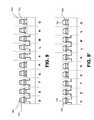
- FIG. 8is a cross-sectional side view illustration of various micro LED structures in accordance with an embodiment of the invention.
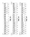
- FIGS. 9 - 9 ′are cross-sectional side view illustrations of the formation of contact openings in a micro LED array in accordance with an embodiment of the invention.
- FIGS. 10 - 10 ′′are cross-sectional side view illustrations of the formation of contact openings in a micro LED array in accordance with an embodiment of the invention.
- FIGS. 11A-11Care cross sectional side view illustrations of a wicked up bonding layer in accordance with an embodiment of the invention.
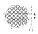
- FIGS. 12A-12Binclude top and cross-sectional side view illustrations of a carrier wafer and array of micro LED structures including micro p-n diodes in accordance with an embodiment of the invention.
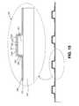
- FIG. 13is an illustration of a method of picking up and transferring a micro LED structure from a carrier substrate to a receiving substrate in accordance with an embodiment of the invention.
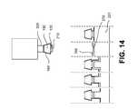
- FIG. 14is a cross-sectional side view illustration of a transfer head picking up a micro LED structure from a carrier substrate in accordance with an embodiment of the invention.
- FIG. 15is a cross-sectional side view illustration of a bipolar micro device transfer head in accordance with an embodiment of the invention.
- FIG. 16is a cross-sectional side view illustration of a receiving substrate with a plurality of micro LEDs in accordance with an embodiment of the invention.
- Embodiments of the present inventiondescribe micro semiconductor devices and a method of forming an array of micro semiconductor devices such as micro light emitting diodes (LEDs) for transfer to a receiving substrate.
- the receiving substratemay be, but is not limited to, a display substrate, a lighting substrate, a substrate with functional devices such as transistors or integrated circuits (ICs), or a substrate with metal redistribution lines.
- ICsintegrated circuits
- embodiments of the present inventionare described with specific regard to micro LEDs comprising p-n diodes, it is to be appreciated that embodiments of the invention are not so limited and that certain embodiments may also be applicable to other micro semiconductor devices which are designed in such a way so as to perform in a controlled fashion a predetermined electronic function (e.g. diode, transistor, integrated circuit) or photonic function (LED, laser).
- a predetermined electronic functione.g. diode, transistor, integrated circuit
- LEDphotonic function
- spanning,” “over,” “to,” “between” and “on” as used hereinmay refer to a relative position of one layer with respect to other layers.
- One layer “spanning,” “over” or “on” another layer or bonded “to” another layermay be directly in contact with the other layer or may have one or more intervening layers.
- One layer “between” layersmay be directly in contact with the layers or may have one or more intervening layers.
- micro devicemay refer to the descriptive size of certain devices or structures in accordance with embodiments of the invention.
- micro devices or structuresare meant to refer to the scale of 1 to 100 ⁇ m.
- embodiments of the present inventionare not necessarily so limited, and that certain aspects of the embodiments may be applicable to larger, and possibly smaller size scales.
- embodiments of the inventiondescribe a method of processing a bulk LED substrate into an array of micro LED structures which are poised for pick up and transfer to a receiving substrate.
- the micro LED structurescan be picked up and transferred individually, in groups, or as the entire array.
- the micro LED structures in the array of micro LED structuresare poised for pick up and transfer to a receiving substrate such as display substrate of any size ranging from micro displays to large area displays, and at high transfer rates.
- arrays of micro LED structures which are poised for pick upare described as having a 10 ⁇ m by 10 ⁇ m pitch, or 5 ⁇ m by 5 ⁇ m pitch.
- a 6 inch substratefor example, can accommodate approximately 165 million micro LED structures with a 10 ⁇ m by 10 ⁇ m pitch, or approximately 660 million micro LED structures with a 5 ⁇ m by 5 ⁇ m pitch.
- a high density of pre-fabricated micro devices with a specific functionalitymay be produced in a manner in which they are poised for pick up and transfer to a receiving substrate.
- the techniques described hereinare not limited to micro LED structures, and may also be used in the manufacture of other micro devices.
- embodiments of the inventiondescribe a micro LED structure and micro LED array in which each micro p-n diode is formed over a respective location of a bonding layer.
- the respective locations of the bonding layermay or may not be laterally separate locations.
- An operationmay be performed on a respective location of the bonding layer corresponding to a micro LED during the micro LED pick up process in which the respective location of the bonding layer undergoes a phase change which assists in the pick up process.
- the respective location of the bonding layermay change from solid to liquid in response to a temperature cycle.
- the respective location of the bonding layermay retain the micro p-n diode in place on a carrier substrate through surface tension forces, while also providing a medium from which the micro p-n diode is readily releasable.
- the liquid statemay act as a cushion or shock absorber to absorb forces exerted by a transfer head if a transfer head makes contact with the micro LED structure during the pick up process. In this manner, the liquid state may compensate for non-uniformities in the topography in the micro LED array or transfer head array by smoothing out over the underlying surface in response to compressive forces exerted by a transfer head.
- the respective location of the bonding layermay not undergo a complete phase transformation.
- the respective location of the bonding layermay become substantially more malleable in response to a temperature cycle while partially remaining in the solid state.
- the respective location of the bonding layermay undergo a crystal phase transformation in response to an operation, such as a temperature cycle.
- a semiconductor device layer 110may be formed on a substrate 101 .
- semiconductor device layer 110may include one or more layers and is designed in such a way so as to perform in a controlled fashion a predetermined electronic function (e.g. diode, transistor, integrated circuit) or photonic function (LED, laser).
- a predetermined electronic functione.g. diode, transistor, integrated circuit
- LED, laserphotonic function
- semiconductor device layer 110may be designed in such a way so as to perform in a controlled fashion in a predetermined function, that the semiconductor device layer 110 may not be fully functionalized.
- contactssuch as an anode or cathode may not yet be formed.
- semiconductor device layer 110as a p-n diode layer 110 grown on a growth substrate 101 in accordance with conventional heterogeneous growth conditions.
- the p-n diode layer 110may include a compound semiconductor having a bandgap corresponding to a specific region in the spectrum.
- the p-n diode layer 110may include one or more layers based on II-VI materials (e.g. ZnSe) or III-V nitride materials (e.g. GaN, AN, InN, and their alloys).
- Growth substrate 101may include any suitable substrate such as, but not limited to, silicon, SiC, GaAs, GaN and sapphire (Al 2 O 3 ).
- growth substrate 101is sapphire
- the p-n diode layer 110is formed of GaN.
- sapphirehas a larger lattice constant and thermal expansion coefficient mismatch with respect to GaN, sapphire is reasonably low cost, widely available and its transparency is compatible with excimer laser-based lift-off (LLO) techniques.
- another materialsuch as SiC may be used as the growth substrate 101 for a GaN p-n diode layer 110 .
- SiC substratesmay be transparent.
- MOCVDmetalorganic chemical vapor deposition
- GaNfor example, can be grown by simultaneously introducing trimethylgallium (TMGa) and ammonia (NH 3 ) precursors into a reaction chamber with the sapphire growth substrate 101 being heated to an elevated temperature such as 800° C. to 1,000° C.
- TMGatrimethylgallium
- NH 3ammonia
- p-n diode layer 110may include a bulk GaN layer 112 , an n-doped layer 114 , a quantum well 116 and p-doped layer 118 .
- the bulk GaN layer 112may be n-doped due to silicon or oxygen contamination, or intentionally doped with a donor such as silicon.
- N-doped GaN layer 114may likewise be doped with a donor such as silicon, while p-doped layer 118 may be doped with an acceptor such as magnesium.
- p-n diode configurationsmay be utilized to form p-n diode layer 110 .
- p-n diode layer 110may be utilized to form p-n diode layer 110 .
- p-n diode layer 110may be utilized to form quantum well 116 .
- buffer layersmay be included as appropriate.
- the sapphire growth substrate 101has a thickness of approximately 200 ⁇ m
- bulk GaN layer 112has a thickness of approximately 5 ⁇ m
- n-doped layer 114has a thickness of approximately 0.1 ⁇ m-3 ⁇ m
- quantum well layer 116has a thickness less than approximately 0.3 ⁇ m
- p-doped layer 118has a thickness of approximately 0.1 ⁇ m-1 ⁇ m.
- a metallization layer 120may then be formed over the p-n diode layer 110 .
- metallization layer 120may include an electrode layer 122 and optionally a barrier layer 124 , though other layers may be included.
- metallization layerhas a thickness of approximately 0.1 ⁇ m-2 ⁇ m.
- Electrode layer 122may make ohmic contact to the p-doped GaN layer 118 , and may be formed of a high work-function metal such as Ni, Au, Ag, Pd and Pt.
- electrode layer 122may be reflective to light emission.
- electrode layer 122may also be transparent to light emission. Transparency may be accomplished by making the electrode layer very thin to minimize light absorption.
- Barrier layer 124may optionally be included in the metallization layer 120 to prevent diffusion of impurities into the p-n diode 110 .
- barrier layer 124may include, but is not limited to, Pd, Pt, Ni, Ta, Ti and TiW. In certain embodiments, barrier layer 124 may prevent the diffusion of components from the bonding layer into the p-n diode layer 110 .
- p-n diode layer 110 and metallization layer 120are grown on a growth substrate 101 and subsequently transferred to a carrier substrate 201 , such as one illustrated in FIGS. 2A-2E and described in more detail in the following description.
- the metallization layer 120 and p-n diode layer 110can be patterned prior to transfer to a carrier substrate 201 .
- the carrier substrate 201 and bonding layer 210may also be patterned prior to transfer of the p-n diode layer 110 and metallization layer 120 to the carrier substrate 201 . Accordingly, embodiments of the invention may be implemented in a multitude of variations during formation of an array of micro LEDs for subsequent transfer to a receiving substrate.
- metallization layer 120may be patterned prior to transfer to a carrier substrate 201 .
- the structure of FIG. 1Bmay be achieved by forming a patterned photoresist layer over the p-n diode layer 110 followed by deposition of the metallization layer 120 .
- the photoresist layeris then lifted off (along with the portion of the metallization layer on the photoresist layer) leaving behind the laterally separate locations of metallization layer 120 illustrated in FIG. 1B .
- the pitch of the laterally separate locations of metallization layer 120may be 5 ⁇ m, 10 ⁇ m, or larger corresponding to the pitch of the array of micro LEDs.
- a 5 ⁇ m pitchmay be formed of 3 ⁇ m wide laterally separate locations of metallization layer 120 separated by a 2 ⁇ m spacing.
- a 10 ⁇ m pitchmay be formed of 8 ⁇ m wide separate locations of metallization layer 120 separated by a 2 ⁇ m spacing.
- these dimensionsare meant to be exemplary and embodiments of the invention are not so limited.
- the width of the laterally separate locations of metallization layer 120is less than or equal to the width of the bottom surface of the array of micro p-n diodes 150 as discussed in further detail in the following description and figures.
- patterning of the metallization layer 120may be followed by patterning of p-n diode layer 110 .
- the structure of FIG. 1Cmay be achieved by forming a second patterned photoresist layer over the laterally separate locations of metallization layer 120 and an etchant is applied to etch the p-n diode layer 110 to etch trenches 134 and form a plurality of micro mesas 130 .
- an etchantis applied to etch the p-n diode layer 110 to etch trenches 134 and form a plurality of micro mesas 130 .
- etchingis performed to etch trenches through the p-doped layer 118 , quantum well 116 , and into the n-doped layer 114 or bulk layer 112 .
- Etching of the GaN p-n diode layer 110can be performed utilizing dry plasma etching techniques such as reactive ion etching (RIE), electro-cyclotron resonance (ECR), inductively coupled plasma reactive ion etching ICP-RIE, and chemically assisted ion-beam etching (CAIBE).
- RIEreactive ion etching
- ECRelectro-cyclotron resonance
- ICP-RIEinductively coupled plasma reactive ion etching
- CAIBEchemically assisted ion-beam etching
- the etch chemistriesmay be halogen-based, containing species such as Cl 2 , BCl 3 or SiCl 4 . In the particular embodiment illustrated in FIG.
- micro mesas 130may have tapered sidewalls 132 up to 15 degrees.
- RIEwith a chlorine-based etch chemistry may be utilized.
- the sidewallsmay be vertical.
- ICP-RIEwhich a chlorine-based etch chemistry may be utilized to obtain vertical sidewalls.
- the pitch of the micro mesas 130may be 5 ⁇ m, 10 ⁇ m, or larger.
- a micro mesa 130 array with a 5 ⁇ m pitchmay be formed of 3 ⁇ m wide micro mesas separated by a 2 ⁇ m spacing.
- a micro mesa 130 array with a 10 ⁇ m pitchmay be formed of 8 ⁇ m wide micro mesas separated by a 2 ⁇ m spacing. Though, these dimensions are meant to be exemplary and embodiments of the invention are not so limited.
- FIGS. 2A-2Eare cross-sectional side view illustrations of various embodiments of a carrier substrate 201 with bonding layer 210 for bonding to the metallization layer 120 on growth substrate 101 .
- FIG. 2Aillustrates a carrier substrate 201 and bonding layer 210 which are not patterned prior to bonding.
- FIGS. 2B-2Dillustrate a carrier substrate 201 which has been patterned to form a plurality of posts 202 having sidewalls 204 and separated by trenches 206 .
- Posts 202may have a maximum width which is equal to or less than a width of the micro p-n diodes 135 , 150 , as will become more apparent in the following description and figures.
- the trench posts 202are at least twice as tall as a thickness of the bonding layer 210 .
- bonding layer 210may have a thickness of approximately 0.1 ⁇ m-2 ⁇ m, and trench posts have a height of at least 0.2 ⁇ m-4 ⁇ m.
- a conformal bonding layer 210is formed over the posts 202 , and on the sidewalls 204 and within trenches 206 .
- bonding layer 210is anisotropically deposited so that it is formed only on the top surface of posts 202 and within the trenches 206 , without a significant amount being deposited on the sidewalls 204 .
- bonding layer 210is formed only on the top surface of posts 202 .
- Such a configurationmay be formed by patterning the posts 202 and bonding layer 210 with the same patterned photoresist.
- the laterally separate locations of the bonding layer 210may be formed with a photoresist lift off technique in which a blanket layer of the bonding layer is deposited over a patterned photoresist layer, which is then lifted off (along with the portion of the bonding layer on the photoresist layer) leaving behind the laterally separate locations of the bonding layer 210 illustrated in FIG. 2E , though other processing techniques may be used.
- certain embodiments of the inventioninclude laterally separate locations of the metallization layer 120 and/or laterally separate locations of the bonding layer 210 .
- FIG. 2Bin which a conformal bonding layer 210 is formed over the posts 202 , and on the sidewalls 204 and within trenches 206 , the particular locations of the bonding layer on top of the posts 202 are laterally separated by the trenches 206 .
- the locations of the bonding layer 210 on top of the posts 202are laterally separate locations.
- the individual discrete locations of the bonding layer 210 in FIG. 2Eare laterally separated by the space between them. Where posts 202 exist, the relationship of the bonding layer 210 thickness to post 202 height may factor into the lateral separation of the locations of the bonding layer 210 .
- Bonding layer 210may be formed from a variety of suitable materials. Bonding layer may be formed from a material which is capable of adhering a micro LED structure to a carrier substrate. In an embodiment, bonding layer 210 may undergo a phase change in response to an operation such as change in temperature. In an embodiment, bonding layer may be removable as a result of the phase change. In an embodiment, bonding layer may be remeltable or reflowable. In an embodiment, the bonding layer may have a liquidus temperature or melting temperature below approximately 350° C., or more specifically below approximately 200° C. At such temperatures the bonding layer may undergo a phase change without substantially affecting the other components of the micro LED structure.
- the bonding layermay be formed of a metal or metal alloy, or of a thermoplastic polymer which is removable.
- the bonding layermay be conductive.
- the bonding layerundergoes a phase change from solid to liquid in response to a change in temperature a portion of the bonding layer may remain on the micro LED structure during the pick up operation as described in more detail the following description.
- the portion of conductive bonding layer remaining on the micro LED structure during the transfer operationmay aid in bonding the micro LED structure to a conductive pad on the receiving substrate.
- Soldersmay be suitable materials for bonding layer 210 since many are generally ductile materials in their solid state and exhibit favorable wetting with semiconductor and metal surfaces.
- a typical alloymelts not a single temperature, but over a temperature range.
- solder alloysare often characterized by a liquidus temperature corresponding to the lowest temperature at which the alloy remains liquid, and a solidus temperature corresponding to the highest temperature at which the alloy remains solid.
- An exemplary list of low melting solder materialswhich may be utilized with embodiments of the invention are provided in Table 1.
- thermoplastic polymerswhich may be utilized with embodiments of the invention are provided in Table 2.
- bonding layer 210is formed with a uniform thickness and may be deposited by a variety of suitable methods depending upon the particular composition.
- solder compositionsmay be sputtered, deposited by electron beam (E-beam) evaporation, or plated with a seed layer to obtain a uniform thickness.
- E-beamelectron beam
- Posts 202may be formed from a variety of materials and techniques.
- posts 202may be formed integrally with carrier substrate 201 by patterning the carrier substrate 201 by an etching or embossing process.
- carrier substrate 201may be a silicon substrate with integrally formed posts 202 .
- postscan be formed on top of carrier substrate 201 .
- posts 202may be formed by a plate up and photoresist lift off technique.
- Postscan be formed from any suitable material including semiconductors, metals, polymers, dielectrics, etc.
- the growth substrate 101 and carrier substrate 201may be bonded together under heat and/or pressure. It is to be appreciated that while FIG. 3 illustrates the bonding of the patterned structure of FIG. 1B with the unpatterned structure of FIG. 2A , that any combination of FIGS. 1A-1C and FIGS. 2A-2E are contemplated in accordance with embodiments of the invention.
- bonding layer 210is formed on the carrier substrate 201 prior to bonding, it is also possible that the bonding layer 210 is formed on the metallization layer 120 of the growth substrate 101 prior to bonding.
- bonding layer 210could be formed over metallization layer 120 , and patterned with metallization layer 120 during formation of the laterally separate locations of metallization layer illustrated in FIG. 1B .
- an oxidation resistant filmmay be formed on the top surface of either or both substrates to prevent oxidation prior to bonding.
- a thin gold filmcan be deposited on either or both of the exposed surface of metallization layer 120 and bonding layer 210 .
- the bonding layer 210may partially soak up the gold film resulting in a gold alloy at the bonding interface between the substrates.
- FIG. 4is a cross-sectional side view illustration of various non-limiting possible structures after bonding the growth substrate 101 and carrier substrate 201 .
- the particular combinations of substratesare described in Table 3.
- the particular embodiment illustrated in Example 4Arepresents the bonding of the carrier substrate illustrated in FIG. 2D to the growth substrate illustrated in FIG. 1C .
- the structures of many of the examplescan also be created by forming the bonding layer 210 on the growth substrate, followed by bonding the growth substrate 101 to the carrier substrate 201 .
- example 4Ocan also be created by patterning bonding layer 210 and metallization layer 210 on growth substrate 101 , following by bonding the growth substrate 101 to carrier substrate 201 .
- the growth substrate 101has been removed from the bonded structure.
- Growth substrate 101may be removed by a suitable method such as chemical etching or an excimer laser-based lift-off (LLO) if the growth substrate is transparent.
- LLO of a GaN p-n diode layer 110 from a transparent sapphire growth substrate 101is accomplished by irradiating the 101 / 110 layer interface through the transparent sapphire growth substrate 101 with a short pulse (e.g. tens of nanoseconds) from an ultraviolet laser such as a Nd-YAG laser or KrF excimer laser.
- the transparent sapphire growth substrate 101can be removed by remelting the Ga on a hotplate.
- the p-n diode layer 110is thinned down to a desirable thickness.
- a predetermined amount of the bulk GaN layer 112 (which may be n-type) or a portion of the n-type GaN layer 114are removed so that an operable p-n diode remains after thinning.
- the thinning processmay be performed utilizing suitable techniques such as polishing, wet etching or dry etching. For example, a combination of polish and/or timed etch to a desired thickness may be performed.
- a timed etch to a desired thicknessmay be performed in order to avoid damaging the patterned structures.
- a timed etch to a desired thicknessmay be performed in order to avoid damaging the patterned structures.
- a patterned mask layer 140may be formed over the unpatterned p-n diode layer 110 for etching of p-n diode layer 110 to form free standing micro p-n diodes 150 .
- Mask layer 140may be formed from photoresist or a variety of materials such as metal (e.g. chromium, nickel) or dielectric (silicon nitride, silicon oxide) which are more resistant to the GaN etching conditions than is photoresist.
- Etching of the GaN p-n diode layer 110can be performed utilizing dry plasma etching techniques such as reactive ion etching (RIE), electro-cyclotron resonance (ECR), inductively coupled plasma reactive ion etching (ICP-RIE), and chemically assisted ion-beam etching (CAIBE).
- RIEreactive ion etching
- ECRelectro-cyclotron resonance
- ICP-RIEinductively coupled plasma reactive ion etching
- CAIBEchemically assisted ion-beam etching
- the etch chemistriesmay be halogen-based, containing species such as Cl 2 , BCl 3 or SiCl 4 .
- micro p-n diodes 150may have outwardly tapered sidewalls 153 (from top to bottom of the micro p-n diodes 150 ) up to 15 degrees.
- RIEwith a chlorine-based etch chemistry may be utilized.
- the sidewalls 153may be vertical.
- ICP-RIEwhich a chlorine-based etch chemistry may be utilized to obtain vertical sidewalls.
- outwardly tapered sidewallsmay be advantageous in some embodiments when forming a common contact over a series of micro LED structures which have been picked up and transferred to a receiving substrate.
- the pitch between the micro p-n diodes 150may be 5 ⁇ m, 10 ⁇ m, or larger.
- a micro p-n diode 150 array with a 5 ⁇ m pitchmay be formed of 3 ⁇ m wide micro p-n diodes separated by a 2 ⁇ m spacing.
- a micro p-n diode 150 array with a 10 ⁇ m pitchmay be formed of 8 ⁇ m wide micro p-n diodes separated by a 2 ⁇ m spacing.
- etchingmay optionally be continued on metallization layer 120 and/or bonding layer 210 utilizing suitable etching chemistries based upon the particular materials in metallization layer 120 and bonding layer 210 .
- anisotropic etching with a dry etching chemistrycan be utilized to etch metallization layer 120 and/or bonding layer 210 so that the layers 120 , 210 have a width matching the overlying lower surface of the micro p-n diode 150 .
- FIG. 7 ′anisotropic etching with a dry etching chemistry can be utilized to etch metallization layer 120 and/or bonding layer 210 so that the layers 120 , 210 have a width matching the overlying lower surface of the micro p-n diode 150 .
- wet etchingmay be utilized to “undercut” the metallization layer 120 and/or bonding layer 210 underneath the overlying lower surface of the micro p-n diode 150 as illustrated in Examples 7′′D-7′′H. While not specifically illustrated, it is understood that etching could also be performed to “undercut” the underlying layers 120 , 210 underneath micro p-n diodes 135 .
- the mask layer 140may be removed, for example by using a selective etching technique, resulting the micro LED array illustrated in FIG. 8 .
- the micro LED arrayincludes a carrier substrate 201 , a plurality of locations of a bonding layer 210 (which may or may not be laterally separate) on the carrier substrate, and a respective plurality of separate micro p-n diodes 135 , 150 over the plurality of locations of the bonding layer 210 .
- a plurality of separate locations of metallization layer 120are formed between the respective plurality of separate micro p-n diodes 135 , 150 and the plurality of locations of the bonding layer 210 .
- the carrier substrateincludes a respective plurality of pillars 202 on which the plurality of laterally separate locations of the bonding layer 210 are formed, as illustrated in Examples 8A-8F and Examples 8K-8M.
- the micro p-n diodes 150(as well as micro p-n diodes 135 ) include a top surface 152 and a bottom surface 151
- the metallization layer 120includes a top surface 121 and a bottom surface
- the bottom surface 151 of the micro p-n diode 150(as well as micro p-n diodes 135 ) is wider than the top surface 121 of the metallization layer 120 .
- the plurality of micro p-n diodes 135 , 150each include a bottom surface 151 which has approximately the same width as a top surface 203 of each of the respective plurality of pillars 202 . In other embodiments, the plurality of micro p-n diodes 135 , 150 each include a bottom surface 151 which is wider than a top surface 203 of each of the respective plurality of pillars 202 . The relationship of the micro p-n diode 135 , 150 bottom width and underlying pillar 202 top surface may affect the pick up process.
- the micro p-n diode 135 , 150is essentially floating on a liquid layer.
- Surface tension forces in the liquid bonding layer 210may retain the micro p-n diode 135 , 150 in place on top of the pillar 202 .
- surface tension forces associated with the edges of the top surface of the pillar 202may further assist in maintaining the micro p-n diode 135 , 150 in place where the pillar 202 top surface width is less than or approximately equal to the p-n diode 135 , 150 bottom width.
- the plurality of micro p-n diodes 135 , 150are positioned over an unpatterned bonding layer 210 .
- the bonding layer 210may be a uniform layer on the carrier substrate and the corresponding plurality of locations of the bonding layer 210 are not laterally separate from each other.
- the plurality of micro p-n diodes 135 , 150are positioned over a pattered bonding layer 210 .
- the patterned bonding layermay include a plurality of laterally separate locations of the bonding layer 210 .
- the plurality of micro p-n diodes 135 , 150each include a bottom surface 151 which has approximately the same or greater width than a corresponding top surface 211 for a plurality of laterally separate locations of the bonding layer 210 .
- the bonding layermay absorb compression forces associated with contacting the micro LED structure with a transfer head during the pick up process. As a result, the bonding layer may absorb the compressive forces and bulge out laterally.
- each micro LED structureis patterned to have a small separation distance, of 2 ⁇ m for example, the amount of bonding layer laterally protruding from each micro LED structure should be minimized so as to not interfere with an adjacent micro LED structure during the pick up process.
- the trenchesmay act as bonding layer reservoirs into which molten bonding layer may flow without interfering with an adjacent micro LED structure.
- the micro LED structures or array of micro LED structures of FIG. 8(as well as the micro LED structures of FIG. 6 Example 6I, and FIG. 7 Examples 7′D-7′I after removal of layer 140 ) are poised for pick up and transfer to a receiving substrate, for example with a transfer head 300 described in more detail with regard to FIGS. 14-16 .
- a thin conformal dielectric barrier layermay be formed of an array of any of the micro p-n diodes 135 , 150 prior to pick up and transfer to a receiving substrate.
- a thin conformal dielectric barrier layer 160may be formed over an array of any of the micro p-n diodes 150 of FIGS.
- the thin conformal dielectric barrier layer 160may protect against charge arcing between adjacent micro p-n diodes 150 during the pick up process, and thereby protect against adjacent micro p-n diodes 150 from sticking together during the pick up process.
- the thin conformal dielectric barrier layer 160may also protect the sidewalls 153 , quantum well layer 116 and bottom surface 151 , of the micro p-n diodes 150 from contamination which could affect the integrity of the micro p-n diodes 150 .
- the thin conformal dielectric barrier layer 160can function as a physical barrier to wicking of the bonding layer material 210 up the sidewalls and quantum layer 116 of the micro p-n diodes 150 as described in more detail with regard to FIGS. 11A-11C in the following description.
- the thin conformal dielectric barrier layer 160may also insulate the micro p-n diodes 150 once placed on a receiving substrate.
- the thin conformal dielectric barrier layer 160is approximately 50-600 angstroms thick aluminum oxide (Al 2 O 3 ).
- Conformal dielectric barrier layer 160may be deposited by a variety of suitable techniques such as, but not limited to, atomic layer deposition (ALD).
- the thin conformal dielectric layer and contact openingscan be formed using a mask layer lift off technique.
- the mask layer 140 illustrated in FIG. 7 for patterning the micro p-n diode 150can also be used in a lift off technique for forming the thin conformal dielectric barrier layer 160 and contact opening 162 .
- the thin conformal dielectric barrier layer 160may be formed over an array of any of the micro p-n diodes 150 of FIG. 7 , FIG. 7 ′ or FIG. 7 ′′ and is conformal to and spans across exposed surfaces of the mask layer 140 , and sidewalls 153 and the bottom surface 151 of the p-n diode 150 .
- the conformal dielectric barrier layer 160may also span across exposed surfaces of metallization layer 120 , bonding layer 210 , as well as the carrier substrate and posts 202 , if present.
- the mask layer 140is then removed, lifting off the portion of the thin conformal dielectric barrier layer 160 formed thereon resulting in the structure illustrated in FIG. 9 ′ including contact openings 162 .
- the conformal dielectric barrier layer 160is not formed on the top surface 152 of the micro p-n diodes 150 .
- the thin conformal dielectric layercan also be formed over the array of micro p-n diodes 135 , 150 of FIG. 8 (as well as the micro LED structures of FIG. 6 Example 6I, and FIG. 7 Examples 7′D-7′I after removal of layer 140 ) followed by patterning to create contact openings 162 .
- the thin conformal dielectric barrier layer 160may be formed over an array of any of the micro p-n diodes 150 and is conformal to and spans across the exposed top surface and sidewalls of the p-n diodes 150 .
- the dielectric barrier layer 160may also span across the exposed bottom surface 151 of the p-n diodes 135 , 150 and surfaces of metallization layer 120 , bonding layer 210 , as well as the carrier substrate 201 and posts 202 , if present.
- a blanket photoresist layermay then be formed over the p-n diode array and carrier substrate 201 , and then patterned to form openings over each micro p-n diode 135 , 150 .
- the thin conformal dielectric barrier layer 160may then be etched to form contact openings 162 on the top surface of each micro p-n diode 135 , 150 . Contact openings 162 are illustrated in FIGS. 10 ′- 10 ′′ after removal of the patterned photoresist.
- contact openings 162may have a slightly smaller width than the top surface of the micro p-n diodes 135 , 150 .
- the difference in widthmay be a result of adjusting for an alignment tolerance in patterning the photoresist.
- the conformal dielectric barrier layer 160may form a lip around the top surface and sidewalls of the micro p-n diodes 135 , 150 .
- contact openings 162may have a slightly larger width than the top surface of the micro p-n diodes 135 , 150 . In the embodiment illustrated in FIG.
- the contact openings 162expose the top surfaces of the micro p-n diodes 150 and an upper portion of the sidewalls of the micro p-n diodes 150 , while the dielectric barrier layer 160 covers and insulates the quantum well layers 116 .
- an amount of bonding layer 210wicks up along the side surfaces of the metallization layer 120 and along the bottom surface 151 of the p-n diode layer 110 during the bonding operation illustrated in FIG. 3 .
- FIG. 10Bit is possible that after forming the micro p-n diodes 150 , that the amount bonding layer 210 which has wicked up could potentially continue its migration along the sidewalls 153 of the micro p-n diode 150 during subsequent processing. Continued migration toward the quantum well layer 116 could interfere with the operation of the micro p-n diode 150 .
- the conformal dielectric barrier layer 160may function as a physical barrier to protect the sidewalls 153 and quantum well layer 116 of the micro p-n diodes 150 from contamination by the bonding layer material 210 during subsequent temperature cycles (particularly at temperatures above the liquidus or melting temperature of the bonding layer material 210 ) such as during picking up the micro device from the carrier substrate, and releasing the micro device onto the receiving substrate. While FIGS.
- FIGS. 12A-12Binclude top and cross-sectional side view illustrations of a carrier substrate 201 and array of micro LED structures in accordance with an embodiment of the invention.
- the arraysare produced from micro LED structures of Example 10′N including micro p-n diode 150 .
- FIGS. 12A-12Bare meant to be exemplary, and that the array of micro LED structures can be formed from any of the micro LED structures previously described. In the embodiment illustrated in FIG.
- each individual micro p-n diode 150is illustrated as a pair of concentric circles having different diameters or widths corresponding the different widths of the top and bottom surfaces of the micro p-n diode 150 , and the corresponding tapered sidewalls spanning between the top and bottom surfaces.
- each individual micro p-n diode 150is illustrated as a pair of concentric squares with tapered or rounded corners, with each square having a different width corresponding to the different widths of the top and bottom surfaces of the micro p-n diode 150 , and the corresponding tapered sidewalls spanning from the top and bottom surfaces.
- embodiments of the inventiondo not require tapered sidewalls, and the top and bottom surfaces of the micro p-n diode 150 may have the same diameter, or width, and vertical sidewalls.
- the array of micro LED structuresis described as having a pitch (P), spacing (S) between each micro LED structure and maximum width (W) of each micro LED structure.
- Ppitch
- Sspacing
- Wmaximum width
- x-dimensionsare illustrated by the dotted lines in the top view illustration, though it is understood that similar y-dimensions may exist, and may have the same or different dimensional values.
- the x- and y-dimensional valuesare identical in the top view illustration.
- the array of micro LED structuresmay have a pitch (P) of 10 ⁇ m, with each micro LED structure having a spacing (S) of 2 ⁇ m and maximum width (W) of 8 ⁇ m.
- the array of micro LED structuresmay have a pitch (P) of 5 ⁇ m, with each micro LED structure having a spacing (S) of 2 ⁇ m and maximum width (W) of 3 ⁇ m.
- Ppitch
- Pspacing
- Wmaximum width
- each micro LED structuremay include a micro p-n diode and a metallization layer, with the metallization layer between the micro p-n diode and a bonding layer on the carrier substrate.
- a conformal dielectric barrier layermay optionally span sidewalls of the micro p-n diode.
- the conformal dielectric barrier layermay additionally span a portion of the bottom surface of the micro p-n diode, as well as sidewalls of the metallization layer, and bonding layer if present.
- a phase changeis created in the bonding layer for at least one of the micro LED structures.
- the phase changemay be associated with heating the bonding layer above a melting temperature or liquidus temperature of a material forming the bonding layer or altering a crystal phase of a material forming the bonding layer.
- the micro p-n diode and metallization layer, optionally a portion of the conformal dielectric barrier layer for at least one of the micro LED structures, and optionally a portion of bonding layer 210may then be picked up with a transfer head in operation 1320 and then placed on a receiving substrate in operation 1330 .
- FIG. 14A general illustration of operation 1320 in accordance with an embodiment is provided in FIG. 14 in which a transfer head 300 picks up a micro p-n diode, metallization layer, a portion of the conformal dielectric barrier layer for at least one of the micro LED structures, and a portion of bonding layer 210 .
- a conformal dielectric barrier layerhas been formed, however, in other embodiments a conformal dielectric barrier layer may not be present.
- a portion of bonding layer 210such as approximately half, may be lifted off with the micro LED structure.
- micro LED structure including micro p-n diode 150While a specific micro LED structure including micro p-n diode 150 is illustrated, it is understood than any of the micro LED structures including any of the micro p-n diodes 150 described herein may be picked up.
- FIG. 14shows a transfer head 300 picking up a single micro LED structure, transfer head 300 may pick up a group of micro LED structures in other embodiments.
- the bottom surface of the micro p-n diode 150is wider than the top surface of the metallization layer 120 , and the conformal dielectric barrier layer 160 spans the sidewalls of the micro p-n diode 150 , a portion of the bottom surface of the micro p-n diode 150 and sidewalls of the metallization layer 120 . This may also apply for micro p-n diodes 135 .
- the portion of the conformal dielectric barrier layer 160 wrapping underneath the micro p-n diode 135 , 150protects the conformal dielectric barrier layer 160 on the sidewalls of the micro p-n diode 150 from chipping or breaking during the pick up operation with the transfer head 300 .
- Stress pointsmay be created in the conformal dielectric barrier layer 160 adjacent the metallization layer 120 or bonding layer 210 , particularly at corners and locations with sharp angles. Upon contacting the micro LED structure with the transfer head 300 and/or creating the phase change in the bonding layer, these stress points become natural break points in the conformal dielectric barrier layer 160 at which the conformal dielectric layer can be cleaved.
- the conformal dielectric barrier layer 160is cleaved at the natural break points after contacting the micro LED structure with the transfer head and/or creating the phase change in the bonding layer, which may be prior to or during picking up the micro p-n diode and the metallization layer.
- the bonding layermay smooth out over the underlying structure in response to compressive forces associated with contacting the micro LED structure with the transfer head.
- the transfer headis rubbed across a top surface of the micro LED structure prior to creating the phase change in the bonding layer. Rubbing may dislodge any particles which may be present on the contacting surface of either of the transfer head or micro LED structure.
- Rubbingmay also transfer pressure to the conformal dielectric barrier layer.
- both transferring a pressure from the transfer head 300 to the conformal dielectric barrier layer 160 and heating the bonding layer above a liquidus temperature of the bonding layercan contribute to cleaving the conformal dielectric barrier layer 160 at a location underneath the micro p-n diode 135 , 150 and may preserve the integrity of the micro LED structure and quantum well layer.
- the bottom surface of the micro p-n diode 135 , 150is wider than the top surface of the metallization layer 120 to the extent that there is room for the conformal dielectric barrier layer 160 to be formed on the bottom surface of the micro p-n diode 135 , 150 and create break points, though this distance may also be determined by lithographic tolerances.
- a 0.25 ⁇ m to 1 ⁇ m distance on each side of the micro p-n diode 135 , 150accommodates a 50 angstrom to 600 angstrom thick conformal dielectric barrier layer 160 .
- transfer headscan be utilized to aid in the pick up and placement operations 1320 , 1330 in accordance with embodiments of the invention.
- the transfer head 300may exert a pick up pressure on the micro LED structure in accordance with vacuum, magnetic, adhesive, or electrostatic principles in order to pick up the micro LED structure.
- FIG. 15is a cross-sectional side view illustration of a bipolar micro device transfer head which operates according to electrostatic principles in order to pick up the micro LED structure in accordance with an embodiment of the invention.
- the micro device transfer head 300may include a base substrate 302 , a mesa structure 304 including a top surface 308 and sidewalls 306 , an optional passivation layer 310 formed over the mesa structure 304 and including a top surface 309 and sidewalls 307 , a pair of electrodes 316 A, 316 B formed over the mesa structure 304 (and optional passivation layer 310 ) and a dielectric layer 320 with a top surface 321 covering the electrodes 316 A, 316 B.
- Base substrate 302may be formed from a variety of materials such as silicon, ceramics and polymers which are capable of providing structural support. In an embodiment, base substrate has a conductivity between 10 3 and 10 18 ohm-cm. Base substrate 302 may additionally include wiring (not shown) to connect the micro device transfer heads 300 to the working electronics of an electrostatic gripper assembly.
- FIG. 16is an illustration of a receiving substrate 400 onto which a plurality of micro LED structures have been placed in accordance with an embodiment of the invention.
- the receiving substratemay be, but is not limited to, a display substrate, a lighting substrate, a substrate with functional devices such as transistors, or a substrate with metal redistribution lines.
- each micro LED structuremay be placed over a driver contact 410 .
- a common contact line 420may then be formed over the series of micro p-n diodes 135 , 150 .
- the tapered sidewalls of the micro p-n diodes 135 , 150may provide a topography which facilitates the formation of a continuous contact line.
- the p-n diode 135 , 150may include a top n-doped layer 114 with a thickness of approximately 0.1 ⁇ m-3 ⁇ m, quantum well layer 116 (which may be SQW or MQW) with a thickness less than approximately 0.3 ⁇ m, and lower p-doped layer 118 with thickness of approximately 0.1 ⁇ m-1 ⁇ m.
- top n-doped layer 114may be 0.1 ⁇ m-6 ⁇ m thick (which may include or replace bulk layer 112 previously described).
- p-n diodes 135 , 150may be less than 3 ⁇ m thick, and less than 10 ⁇ m wide.
Landscapes
- Engineering & Computer Science (AREA)
- General Engineering & Computer Science (AREA)
- Physics & Mathematics (AREA)
- Condensed Matter Physics & Semiconductors (AREA)
- General Physics & Mathematics (AREA)
- Manufacturing & Machinery (AREA)
- Computer Hardware Design (AREA)
- Microelectronics & Electronic Packaging (AREA)
- Power Engineering (AREA)
- Led Devices (AREA)
- Photo Coupler, Interrupter, Optical-To-Optical Conversion Devices (AREA)
- Electroluminescent Light Sources (AREA)
- Led Device Packages (AREA)
- Light Receiving Elements (AREA)
Abstract
Description
| TABLE 1 | ||
| Liquidus Temperature | Solidus Temperature | |
| Chemical composition | (° C.) | (° C.) |
| 100 In | 156.7 | 156.7 |
| 66.3In33.7Bi | 72 | 72 |
| 51In32.5Bi16.5Sn | 60 | 60 |
| 57Bi26In17Sn | 79 | 79 |
| 54.02Bi29.68In16.3Sn | 81 | 81 |
| 67Bi33In | 109 | 109 |
| 50In50Sn | 125 | 118 |
| 52Sn48In | 131 | 118 |
| 58Bi42Sn | 138 | 138 |
| 97In3Ag | 143 | 143 |
| 58Sn42In | 145 | 118 |
| 99.3 | 150 | 150 |
| 150 | 125 | |
| 99.4 | 152 | 152 |
| 99.6 | 153 | 153 |
| 99.5In0.5Ga | 154 | 154 |
| 60Sn40Bi | 170 | 138 |
| 100Sn | 232 | 232 |
| 95Sn5Sb | 240 | 235 |
| TABLE 2 | |||
| Melting Temperature | |||
| Polymer | (° C.) | ||
| Acrylic (PMMA) | 130-140 | ||
| Polyoxymethylene (POM or Acetal) | 166 | ||
| Polybutylene terephthalate (PBT) | 160 | ||
| Polycaprolactone (PCL) | 62 | ||
| Polyethylene terephthalate (PET) | 260 | ||
| Polycarbonate (PC) | 267 | ||
| Polyester | 260 | ||
| Polyethylene (PE) | 105-130 | ||
| Polyetheretherketone (PEEK) | 343 | ||
| Polylactic acid (PLA) | 50-80 | ||
| Polypropylene (PP) | 160 | ||
| Polystyrene (PS) | 240 | ||
| Polyvinylidene chloride (PVDC) | 185 | ||
| TABLE 3 | ||||||||||||||||
| Ex. | Ex. | Ex. | Ex. | Ex. | Ex. | Ex. | Ex. | Ex. | Ex. | Ex. | Ex. | Ex. | Ex. | Ex. | ||
| 4A | 4B | 4C | 4D | 4E | 4F | 4G | 4H | 4I | 4J | 4K | 4L | 4M | 4N | 4O | ||
| Carrier | 2D | 2C | 2B | 2D | 2C | 2B | 2A | 2E | 2A | 2E | 2D | 2C | 2B | 2A | 2E |
| Substrate | |||||||||||||||
| (2A-2D) | |||||||||||||||
| Growth | 1C | 1C | 1C | 1A | 1A | 1A | 1A | 1A | 1C | 1C | 1B | 1B | 1B | 1B | 1B |
| Substrate | |||||||||||||||
| (1B) | |||||||||||||||
Claims (18)
Priority Applications (19)
| Application Number | Priority Date | Filing Date | Title |
|---|---|---|---|
| US13/372,258US8794501B2 (en) | 2011-11-18 | 2012-02-13 | Method of transferring a light emitting diode |
| PCT/US2012/064232WO2013074375A1 (en) | 2011-11-18 | 2012-11-08 | Method of forming a micro light emitting diode array |
| AU2012339942AAU2012339942B2 (en) | 2011-11-18 | 2012-11-08 | Micro light emitting diode |
| KR1020147016754AKR101596382B1 (en) | 2011-11-18 | 2012-11-08 | Method of transferring a light emitting diode |
| EP12849007.5AEP2780953B1 (en) | 2011-11-18 | 2012-11-08 | Micro light emitting diode |
| KR1020147016682AKR101704152B1 (en) | 2011-11-18 | 2012-11-08 | A micro light emitting diode |
| BR112014011802ABR112014011802A2 (en) | 2011-11-18 | 2012-11-08 | micro led light |
| PCT/US2012/064231WO2013074374A1 (en) | 2011-11-18 | 2012-11-08 | Micro light emitting diode |
| MX2014005969AMX340348B (en) | 2011-11-18 | 2012-11-08 | LIGHT EMISSOR MICRODIODE. |
| JP2014542349AJP2015500562A (en) | 2011-11-18 | 2012-11-08 | Micro light emitting diode |
| PCT/US2012/064234WO2013074376A1 (en) | 2011-11-18 | 2012-11-08 | Method of transferring a light emitting diode |
| CN201280066486.8ACN104106132B (en) | 2011-11-18 | 2012-11-08 | Method of delivering light-emitting diodes |
| CN201280066487.2ACN104094422B (en) | 2011-11-18 | 2012-11-08 | Micro light emitting diode |
| TW101142917ATWI566433B (en) | 2011-11-18 | 2012-11-16 | Method of forming a micro-light emitting diode array |
| TW105137548ATWI636585B (en) | 2011-11-18 | 2012-11-16 | Micro light emitting diode array structure |
| TW101142916ATWI527267B (en) | 2011-11-18 | 2012-11-16 | Microluminescent diode |
| TW101142919ATWI535052B (en) | 2011-11-18 | 2012-11-16 | Method of transmitting a light emitting diode |
| US14/312,554US10297712B2 (en) | 2011-11-18 | 2014-06-23 | Micro LED display |
| US16/399,853US12243955B2 (en) | 2011-11-18 | 2019-04-30 | Display and micro device array for transfer to a display substrate |
Applications Claiming Priority (3)
| Application Number | Priority Date | Filing Date | Title |
|---|---|---|---|
| US201161561706P | 2011-11-18 | 2011-11-18 | |
| US201261594919P | 2012-02-03 | 2012-02-03 | |
| US13/372,258US8794501B2 (en) | 2011-11-18 | 2012-02-13 | Method of transferring a light emitting diode |
Related Child Applications (1)
| Application Number | Title | Priority Date | Filing Date |
|---|---|---|---|
| US14/312,554ContinuationUS10297712B2 (en) | 2011-11-18 | 2014-06-23 | Micro LED display |
Publications (2)
| Publication Number | Publication Date |
|---|---|
| US20130126589A1 US20130126589A1 (en) | 2013-05-23 |
| US8794501B2true US8794501B2 (en) | 2014-08-05 |
Family
ID=48094811
Family Applications (7)
| Application Number | Title | Priority Date | Filing Date |
|---|---|---|---|
| US13/372,258Active2032-02-15US8794501B2 (en) | 2011-11-18 | 2012-02-13 | Method of transferring a light emitting diode |
| US13/372,222Active2032-04-28US8809875B2 (en) | 2011-11-18 | 2012-02-13 | Micro light emitting diode |
| US13/372,245Expired - Fee RelatedUS8426227B1 (en) | 2011-11-18 | 2012-02-13 | Method of forming a micro light emitting diode array |
| US13/708,695ActiveUS8552436B2 (en) | 2011-11-18 | 2012-12-07 | Light emitting diode structure |
| US13/708,704ActiveUS8558243B2 (en) | 2011-11-18 | 2012-12-07 | Micro device array for transfer to a receiving substrate |
| US14/312,554Active2033-09-16US10297712B2 (en) | 2011-11-18 | 2014-06-23 | Micro LED display |
| US16/399,853Active2035-10-14US12243955B2 (en) | 2011-11-18 | 2019-04-30 | Display and micro device array for transfer to a display substrate |
Family Applications After (6)
| Application Number | Title | Priority Date | Filing Date |
|---|---|---|---|
| US13/372,222Active2032-04-28US8809875B2 (en) | 2011-11-18 | 2012-02-13 | Micro light emitting diode |
| US13/372,245Expired - Fee RelatedUS8426227B1 (en) | 2011-11-18 | 2012-02-13 | Method of forming a micro light emitting diode array |
| US13/708,695ActiveUS8552436B2 (en) | 2011-11-18 | 2012-12-07 | Light emitting diode structure |
| US13/708,704ActiveUS8558243B2 (en) | 2011-11-18 | 2012-12-07 | Micro device array for transfer to a receiving substrate |
| US14/312,554Active2033-09-16US10297712B2 (en) | 2011-11-18 | 2014-06-23 | Micro LED display |
| US16/399,853Active2035-10-14US12243955B2 (en) | 2011-11-18 | 2019-04-30 | Display and micro device array for transfer to a display substrate |
Country Status (10)
| Country | Link |
|---|---|
| US (7) | US8794501B2 (en) |
| EP (1) | EP2780953B1 (en) |
| JP (1) | JP2015500562A (en) |
| KR (2) | KR101704152B1 (en) |
| CN (2) | CN104094422B (en) |
| AU (2) | AU2012339942B2 (en) |
| BR (1) | BR112014011802A2 (en) |
| MX (1) | MX340348B (en) |
| TW (4) | TWI566433B (en) |
| WO (3) | WO2013074374A1 (en) |
Cited By (145)
| Publication number | Priority date | Publication date | Assignee | Title |
|---|---|---|---|---|
| US20140097418A1 (en)* | 2012-10-04 | 2014-04-10 | Samsung Display Co., Ltd. | Organic light emitting diode display and method for manufacturing the same |
| US20140151630A1 (en)* | 2012-12-04 | 2014-06-05 | Feng-Hsu Fan | Protection for the epitaxial structure of metal devices |
| US9358775B2 (en)* | 2014-07-20 | 2016-06-07 | X-Celeprint Limited | Apparatus and methods for micro-transfer-printing |
| US9368683B1 (en) | 2015-05-15 | 2016-06-14 | X-Celeprint Limited | Printable inorganic semiconductor method |
| US9437782B2 (en) | 2014-06-18 | 2016-09-06 | X-Celeprint Limited | Micro assembled LED displays and lighting elements |
| US9468050B1 (en) | 2014-09-25 | 2016-10-11 | X-Celeprint Limited | Self-compensating circuit for faulty display pixels |
| US9537069B1 (en) | 2014-09-25 | 2017-01-03 | X-Celeprint Limited | Inorganic light-emitting diode with encapsulating reflector |
| US9601356B2 (en) | 2014-06-18 | 2017-03-21 | X-Celeprint Limited | Systems and methods for controlling release of transferable semiconductor structures |
| US9607907B2 (en) | 2014-12-01 | 2017-03-28 | Industrial Technology Research Institute | Electric-programmable magnetic module and picking-up and placement process for electronic devices |
| US9640108B2 (en) | 2015-08-25 | 2017-05-02 | X-Celeprint Limited | Bit-plane pulse width modulated digital display system |
| US9704821B2 (en) | 2015-08-11 | 2017-07-11 | X-Celeprint Limited | Stamp with structured posts |
| US9716082B2 (en) | 2014-08-26 | 2017-07-25 | X-Celeprint Limited | Micro assembled hybrid displays and lighting elements |
| US9741785B2 (en) | 2014-09-25 | 2017-08-22 | X-Celeprint Limited | Display tile structure and tiled display |
| US9761754B2 (en) | 2014-06-18 | 2017-09-12 | X-Celeprint Limited | Systems and methods for preparing GaN and related materials for micro assembly |
| US9773711B2 (en) | 2014-12-01 | 2017-09-26 | Industrial Technology Research Institute | Picking-up and placing process for electronic devices and electronic module |
| US9786646B2 (en) | 2015-12-23 | 2017-10-10 | X-Celeprint Limited | Matrix addressed device repair |
| US9799261B2 (en) | 2014-09-25 | 2017-10-24 | X-Celeprint Limited | Self-compensating circuit for faulty display pixels |
| US9818725B2 (en) | 2015-06-01 | 2017-11-14 | X-Celeprint Limited | Inorganic-light-emitter display with integrated black matrix |
| US9865600B2 (en) | 2014-06-18 | 2018-01-09 | X-Celeprint Limited | Printed capacitors |
| US9871023B2 (en) | 2015-03-20 | 2018-01-16 | Rohinni, LLC | Method for transfer of semiconductor devices |
| US9871345B2 (en) | 2015-06-09 | 2018-01-16 | X-Celeprint Limited | Crystalline color-conversion device |
| US20180021892A1 (en)* | 2016-02-19 | 2018-01-25 | MAX-PLANCK-Gesellschaft zur Förderung der Wissenschaften e.V. | Method and device for reversibly attaching a phase changing metal to an object |
| US9923133B2 (en) | 2010-08-26 | 2018-03-20 | X-Celeprint Limited | Structures and methods for testing printable integrated circuits |
| US9929053B2 (en) | 2014-06-18 | 2018-03-27 | X-Celeprint Limited | Systems and methods for controlling release of transferable semiconductor structures |
| US9928771B2 (en) | 2015-12-24 | 2018-03-27 | X-Celeprint Limited | Distributed pulse width modulation control |
| US9930277B2 (en) | 2015-12-23 | 2018-03-27 | X-Celeprint Limited | Serial row-select matrix-addressed system |
| US9980341B2 (en) | 2016-09-22 | 2018-05-22 | X-Celeprint Limited | Multi-LED components |
| US9991163B2 (en) | 2014-09-25 | 2018-06-05 | X-Celeprint Limited | Small-aperture-ratio display with electrical component |
| US9997399B2 (en) | 2016-08-16 | 2018-06-12 | Mikro Mesa Technology Co., Ltd. | Method for transferring semiconductor structure |
| US9997102B2 (en) | 2016-04-19 | 2018-06-12 | X-Celeprint Limited | Wirelessly powered display and system |
| US9997501B2 (en) | 2016-06-01 | 2018-06-12 | X-Celeprint Limited | Micro-transfer-printed light-emitting diode device |
| US10008465B2 (en) | 2011-06-08 | 2018-06-26 | X-Celeprint Limited | Methods for surface attachment of flipped active components |
| US10008483B2 (en) | 2016-04-05 | 2018-06-26 | X-Celeprint Limited | Micro-transfer printed LED and color filter structure |
| US10050351B2 (en) | 2014-06-18 | 2018-08-14 | X-Celeprint Limited | Multilayer printed capacitors |
| US10062588B2 (en) | 2017-01-18 | 2018-08-28 | Rohinni, LLC | Flexible support substrate for transfer of semiconductor devices |
| US10066819B2 (en) | 2015-12-09 | 2018-09-04 | X-Celeprint Limited | Micro-light-emitting diode backlight system |
| US10084020B2 (en) | 2016-11-29 | 2018-09-25 | Gwangju Institute Of Science And Technology | Micro display having vertically stacked structure and method of forming the same |
| US10091446B2 (en) | 2015-12-23 | 2018-10-02 | X-Celeprint Limited | Active-matrix displays with common pixel control |
| US10102794B2 (en) | 2015-06-09 | 2018-10-16 | X-Celeprint Limited | Distributed charge-pump power-supply system |
| US10103069B2 (en) | 2016-04-01 | 2018-10-16 | X-Celeprint Limited | Pressure-activated electrical interconnection by micro-transfer printing |
| US10109753B2 (en) | 2016-02-19 | 2018-10-23 | X-Celeprint Limited | Compound micro-transfer-printed optical filter device |
| US10133426B2 (en) | 2015-06-18 | 2018-11-20 | X-Celeprint Limited | Display with micro-LED front light |
| US10141215B2 (en) | 2016-11-03 | 2018-11-27 | Rohinni, LLC | Compliant needle for direct transfer of semiconductor devices |
| US10153257B2 (en) | 2016-03-03 | 2018-12-11 | X-Celeprint Limited | Micro-printed display |
| US10150325B2 (en) | 2016-02-29 | 2018-12-11 | X-Celeprint Limited | Hybrid banknote with electronic indicia |
| US10153256B2 (en) | 2016-03-03 | 2018-12-11 | X-Celeprint Limited | Micro-transfer printable electronic component |
| US10150326B2 (en) | 2016-02-29 | 2018-12-11 | X-Celeprint Limited | Hybrid document with variable state |
| US10157880B2 (en) | 2016-10-03 | 2018-12-18 | X-Celeprint Limited | Micro-transfer printing with volatile adhesive layer |
| US10181483B2 (en) | 2010-03-29 | 2019-01-15 | X-Celeprint Limited | Laser assisted transfer welding process |
| US10193025B2 (en) | 2016-02-29 | 2019-01-29 | X-Celeprint Limited | Inorganic LED pixel structure |
| US10189243B2 (en) | 2011-09-20 | 2019-01-29 | X-Celeprint Limited | Printing transferable components using microstructured elastomeric surfaces with pressure modulated reversible adhesion |
| US10198890B2 (en) | 2016-04-19 | 2019-02-05 | X-Celeprint Limited | Hybrid banknote with electronic indicia using near-field-communications |
| US10200013B2 (en) | 2016-02-18 | 2019-02-05 | X-Celeprint Limited | Micro-transfer-printed acoustic wave filter device |
| US10199546B2 (en) | 2016-04-05 | 2019-02-05 | X-Celeprint Limited | Color-filter device |
| US20190049367A1 (en)* | 2016-06-02 | 2019-02-14 | Goertek Inc. | Monolithic integration device and micro total analysis system |
| US10217730B2 (en) | 2016-02-25 | 2019-02-26 | X-Celeprint Limited | Efficiently micro-transfer printing micro-scale devices onto large-format substrates |
| US10224231B2 (en) | 2016-11-15 | 2019-03-05 | X-Celeprint Limited | Micro-transfer-printable flip-chip structures and methods |
| US10222698B2 (en) | 2016-07-28 | 2019-03-05 | X-Celeprint Limited | Chiplets with wicking posts |
| US10230048B2 (en) | 2015-09-29 | 2019-03-12 | X-Celeprint Limited | OLEDs for micro transfer printing |
| US10236195B1 (en) | 2017-12-20 | 2019-03-19 | Mikro Mesa Technology Co., Ltd. | Method for transferring device |
| US10255834B2 (en) | 2015-07-23 | 2019-04-09 | X-Celeprint Limited | Parallel redundant chiplet system for controlling display pixels |
| US10297502B2 (en) | 2016-12-19 | 2019-05-21 | X-Celeprint Limited | Isolation structure for micro-transfer-printable devices |
| US10297585B1 (en) | 2017-12-21 | 2019-05-21 | X-Celeprint Limited | Multi-resolution compound micro-devices |
| US10332868B2 (en) | 2017-01-26 | 2019-06-25 | X-Celeprint Limited | Stacked pixel structures |
| US10347168B2 (en) | 2016-11-10 | 2019-07-09 | X-Celeprint Limited | Spatially dithered high-resolution |
| US10360846B2 (en) | 2016-05-10 | 2019-07-23 | X-Celeprint Limited | Distributed pulse-width modulation system with multi-bit digital storage and output device |
| US10361677B2 (en) | 2016-02-18 | 2019-07-23 | X-Celeprint Limited | Transverse bulk acoustic wave filter |
| US10380930B2 (en) | 2015-08-24 | 2019-08-13 | X-Celeprint Limited | Heterogeneous light emitter display system |
| US10381176B2 (en) | 2013-06-12 | 2019-08-13 | Rohinni, LLC | Keyboard backlighting with deposited light-generating sources |
| US10395966B2 (en) | 2016-11-15 | 2019-08-27 | X-Celeprint Limited | Micro-transfer-printable flip-chip structures and methods |
| US10396137B2 (en) | 2017-03-10 | 2019-08-27 | X-Celeprint Limited | Testing transfer-print micro-devices on wafer |
| US10410905B1 (en) | 2018-05-12 | 2019-09-10 | Rohinni, LLC | Method and apparatus for direct transfer of multiple semiconductor devices |
| US10418501B2 (en) | 2015-10-02 | 2019-09-17 | X-Celeprint Limited | Wafer-integrated, ultra-low profile concentrated photovoltaics (CPV) for space applications |
| US10416425B2 (en) | 2009-02-09 | 2019-09-17 | X-Celeprint Limited | Concentrator-type photovoltaic (CPV) modules, receiver and sub-receivers and methods of forming same |
| US10418331B2 (en) | 2010-11-23 | 2019-09-17 | X-Celeprint Limited | Interconnection structures and methods for transfer-printed integrated circuit elements with improved interconnection alignment tolerance |
| US10438859B2 (en) | 2016-12-19 | 2019-10-08 | X-Celeprint Limited | Transfer printed device repair |
| US10453826B2 (en) | 2016-06-03 | 2019-10-22 | X-Celeprint Limited | Voltage-balanced serial iLED pixel and display |
| US10468397B2 (en) | 2017-05-05 | 2019-11-05 | X-Celeprint Limited | Matrix addressed tiles and arrays |
| US10468363B2 (en) | 2015-08-10 | 2019-11-05 | X-Celeprint Limited | Chiplets with connection posts |
| US10468391B2 (en) | 2017-02-08 | 2019-11-05 | X-Celeprint Limited | Inorganic light-emitting-diode displays with multi-ILED pixels |
| US10475876B2 (en) | 2016-07-26 | 2019-11-12 | X-Celeprint Limited | Devices with a single metal layer |
| US10471545B2 (en) | 2016-11-23 | 2019-11-12 | Rohinni, LLC | Top-side laser for direct transfer of semiconductor devices |
| US10505079B2 (en) | 2018-05-09 | 2019-12-10 | X-Celeprint Limited | Flexible devices and methods using laser lift-off |
| US10504767B2 (en) | 2016-11-23 | 2019-12-10 | Rohinni, LLC | Direct transfer apparatus for a pattern array of semiconductor device die |
| US10522575B2 (en) | 2009-03-26 | 2019-12-31 | X-Celeprint Limited | Methods of making printable device wafers with sacrificial layers |
| US10553752B2 (en) | 2015-12-02 | 2020-02-04 | Samsung Electronics Co., Ltd. | Light-emitting device and display device including the same |
| US10573544B1 (en) | 2018-10-17 | 2020-02-25 | X-Celeprint Limited | Micro-transfer printing with selective component removal |
| US10600671B2 (en) | 2016-11-15 | 2020-03-24 | X-Celeprint Limited | Micro-transfer-printable flip-chip structures and methods |
| US10622700B2 (en) | 2016-05-18 | 2020-04-14 | X-Celeprint Limited | Antenna with micro-transfer-printed circuit element |
| US10629393B2 (en) | 2016-01-15 | 2020-04-21 | Rohinni, LLC | Apparatus and method of backlighting through a cover on the apparatus |
| US10690920B2 (en) | 2018-02-28 | 2020-06-23 | X Display Company Technology Limited | Displays with transparent bezels |
| US10714374B1 (en) | 2019-05-09 | 2020-07-14 | X Display Company Technology Limited | High-precision printed structures |
| US10714001B2 (en) | 2018-07-11 | 2020-07-14 | X Display Company Technology Limited | Micro-light-emitting-diode displays |
| US10739882B2 (en) | 2014-08-06 | 2020-08-11 | Apple Inc. | Electronic device display with array of discrete light-emitting diodes |
| US10748793B1 (en) | 2019-02-13 | 2020-08-18 | X Display Company Technology Limited | Printing component arrays with different orientations |
| US10782002B2 (en) | 2016-10-28 | 2020-09-22 | X Display Company Technology Limited | LED optical components |
| US10790173B2 (en) | 2018-12-03 | 2020-09-29 | X Display Company Technology Limited | Printed components on substrate posts |
| US10796971B2 (en) | 2018-08-13 | 2020-10-06 | X Display Company Technology Limited | Pressure-activated electrical interconnection with additive repair |
| US10796938B2 (en) | 2018-10-17 | 2020-10-06 | X Display Company Technology Limited | Micro-transfer printing with selective component removal |
| US10804880B2 (en) | 2018-12-03 | 2020-10-13 | X-Celeprint Limited | Device structures with acoustic wave transducers and connection posts |
| US10832934B2 (en) | 2018-06-14 | 2020-11-10 | X Display Company Technology Limited | Multi-layer tethers for micro-transfer printing |
| US10832609B2 (en) | 2017-01-10 | 2020-11-10 | X Display Company Technology Limited | Digital-drive pulse-width-modulated output system |
| US10832935B2 (en) | 2017-08-14 | 2020-11-10 | X Display Company Technology Limited | Multi-level micro-device tethers |
| US10836200B2 (en) | 2017-11-13 | 2020-11-17 | X Display Company Technology Limited | Rigid micro-modules with ILED and light conductor |
| US10903267B2 (en) | 2019-04-04 | 2021-01-26 | Bor-Jen Wu | System and method for making micro LED display |
| US10910355B2 (en) | 2018-04-30 | 2021-02-02 | X Display Company Technology Limited | Bezel-free displays |
| US10917953B2 (en) | 2016-03-21 | 2021-02-09 | X Display Company Technology Limited | Electrically parallel fused LEDs |
| WO2021041138A1 (en)* | 2019-08-28 | 2021-03-04 | Semileds Corporation | Method for fabricating (led) dice using laser lift-off from a substrate to a receiving plate |
| US10943946B2 (en) | 2017-07-21 | 2021-03-09 | X Display Company Technology Limited | iLED displays with substrate holes |
| US10944027B2 (en) | 2019-06-14 | 2021-03-09 | X Display Company Technology Limited | Pixel modules with controllers and light emitters |
| US11024608B2 (en) | 2017-03-28 | 2021-06-01 | X Display Company Technology Limited | Structures and methods for electrical connection of micro-devices and substrates |
| US11037912B1 (en) | 2020-01-31 | 2021-06-15 | X Display Company Technology Limited | LED color displays with multiple LEDs connected in series and parallel in different sub-pixels of a pixel |
| US11064609B2 (en) | 2016-08-04 | 2021-07-13 | X Display Company Technology Limited | Printable 3D electronic structure |
| US11062936B1 (en) | 2019-12-19 | 2021-07-13 | X Display Company Technology Limited | Transfer stamps with multiple separate pedestals |
| US11061276B2 (en) | 2015-06-18 | 2021-07-13 | X Display Company Technology Limited | Laser array display |
| US11088121B2 (en) | 2019-02-13 | 2021-08-10 | X Display Company Technology Limited | Printed LED arrays with large-scale uniformity |
| US11094870B2 (en) | 2019-03-12 | 2021-08-17 | X Display Company Technology Limited | Surface-mountable pixel packages and pixel engines |
| US11094571B2 (en) | 2018-09-28 | 2021-08-17 | Rohinni, LLC | Apparatus to increase transferspeed of semiconductor devices with micro-adjustment |
| US11101417B2 (en) | 2019-08-06 | 2021-08-24 | X Display Company Technology Limited | Structures and methods for electrically connecting printed components |
| US11127889B2 (en) | 2019-10-30 | 2021-09-21 | X Display Company Technology Limited | Displays with unpatterned layers of light-absorbing material |
| US11137641B2 (en) | 2016-06-10 | 2021-10-05 | X Display Company Technology Limited | LED structure with polarized light emission |
| US11164934B2 (en) | 2019-03-12 | 2021-11-02 | X Display Company Technology Limited | Tiled displays with black-matrix support screens |
| US11189605B2 (en) | 2018-02-28 | 2021-11-30 | X Display Company Technology Limited | Displays with transparent bezels |
| US11230471B2 (en) | 2016-02-05 | 2022-01-25 | X-Celeprint Limited | Micro-transfer-printed compound sensor device |
| US11251139B2 (en) | 2019-01-22 | 2022-02-15 | X-Celeprint Limited | Secure integrated-circuit systems |
| US11274035B2 (en) | 2019-04-24 | 2022-03-15 | X-Celeprint Limited | Overhanging device structures and related methods of manufacture |
| US11282786B2 (en) | 2018-12-12 | 2022-03-22 | X Display Company Technology Limited | Laser-formed interconnects for redundant devices |
| DE102020125857A1 (en) | 2020-10-02 | 2022-04-07 | Chia-Bin Tsen | System and method for fabricating a micro LED display |
| US11315909B2 (en) | 2019-12-20 | 2022-04-26 | X Display Company Technology Limited | Displays with embedded light emitters |
| US11322460B2 (en) | 2019-01-22 | 2022-05-03 | X-Celeprint Limited | Secure integrated-circuit systems |
| US11341901B2 (en)* | 2019-07-26 | 2022-05-24 | Boe Technology Group Co., Ltd. | Driving backplane, display panel and display device |
| US11483937B2 (en) | 2018-12-28 | 2022-10-25 | X Display Company Technology Limited | Methods of making printed structures |
| US11482979B2 (en) | 2018-12-03 | 2022-10-25 | X Display Company Technology Limited | Printing components over substrate post edges |
| US11488943B2 (en) | 2019-06-14 | 2022-11-01 | X Display Company Technology Limited | Modules with integrated circuits and devices |
| US11528808B2 (en) | 2018-12-03 | 2022-12-13 | X Display Company Technology Limited | Printing components to substrate posts |
| US11538849B2 (en) | 2020-05-28 | 2022-12-27 | X Display Company Technology Limited | Multi-LED structures with reduced circuitry |
| US11626856B2 (en) | 2019-10-30 | 2023-04-11 | X-Celeprint Limited | Non-linear tethers for suspended devices |
| US11637540B2 (en) | 2019-10-30 | 2023-04-25 | X-Celeprint Limited | Non-linear tethers for suspended devices |
| US11884537B2 (en) | 2018-12-03 | 2024-01-30 | X-Celeprint Limited | Enclosed cavity structures |
| US11952266B2 (en) | 2020-10-08 | 2024-04-09 | X-Celeprint Limited | Micro-device structures with etch holes |
| US12006205B2 (en) | 2020-10-08 | 2024-06-11 | X-Celeprint Limited | Micro-device structures with etch holes |
| US12074583B2 (en) | 2021-05-11 | 2024-08-27 | X Display Company Technology Limited | Printing components to adhesive substrate posts |
| US12236825B2 (en) | 2018-08-13 | 2025-02-25 | X Display Company Technology Limited | Redundant pixel layouts |
| US12243955B2 (en) | 2011-11-18 | 2025-03-04 | Apple Inc. | Display and micro device array for transfer to a display substrate |
| US12308353B1 (en) | 2021-07-29 | 2025-05-20 | Apple Inc. | Rotate redundancy method for LED array placement to correct front of screen artifacts |
Families Citing this family (221)
| Publication number | Priority date | Publication date | Assignee | Title |
|---|---|---|---|---|
| DE102008054288A1 (en)* | 2008-11-03 | 2010-05-06 | Osram Gesellschaft mit beschränkter Haftung | Method for producing a flexible light strip |
| US8349116B1 (en) | 2011-11-18 | 2013-01-08 | LuxVue Technology Corporation | Micro device transfer head heater assembly and method of transferring a micro device |
| US8573469B2 (en) | 2011-11-18 | 2013-11-05 | LuxVue Technology Corporation | Method of forming a micro LED structure and array of micro LED structures with an electrically insulating layer |
| US8333860B1 (en) | 2011-11-18 | 2012-12-18 | LuxVue Technology Corporation | Method of transferring a micro device |
| US10115862B2 (en) | 2011-12-27 | 2018-10-30 | eLux Inc. | Fluidic assembly top-contact LED disk |
| US9548332B2 (en)* | 2012-04-27 | 2017-01-17 | Apple Inc. | Method of forming a micro LED device with self-aligned metallization stack |
| US9105492B2 (en) | 2012-05-08 | 2015-08-11 | LuxVue Technology Corporation | Compliant micro device transfer head |
| US9034754B2 (en) | 2012-05-25 | 2015-05-19 | LuxVue Technology Corporation | Method of forming a micro device transfer head with silicon electrode |
| US8569115B1 (en) | 2012-07-06 | 2013-10-29 | LuxVue Technology Corporation | Method of forming a compliant bipolar micro device transfer head with silicon electrodes |
| US8415768B1 (en) | 2012-07-06 | 2013-04-09 | LuxVue Technology Corporation | Compliant monopolar micro device transfer head with silicon electrode |
| US8933433B2 (en) | 2012-07-30 | 2015-01-13 | LuxVue Technology Corporation | Method and structure for receiving a micro device |
| US9557215B2 (en) | 2012-08-17 | 2017-01-31 | Massachusetts Institute Of Technology | Phonon-recyling light-emitting diodes |
| US8791530B2 (en) | 2012-09-06 | 2014-07-29 | LuxVue Technology Corporation | Compliant micro device transfer head with integrated electrode leads |
| US9162880B2 (en) | 2012-09-07 | 2015-10-20 | LuxVue Technology Corporation | Mass transfer tool |
| US8941215B2 (en)* | 2012-09-24 | 2015-01-27 | LuxVue Technology Corporation | Micro device stabilization post |
| US8835940B2 (en) | 2012-09-24 | 2014-09-16 | LuxVue Technology Corporation | Micro device stabilization post |
| US9558721B2 (en) | 2012-10-15 | 2017-01-31 | Apple Inc. | Content-based adaptive refresh schemes for low-power displays |
| US9029880B2 (en) | 2012-12-10 | 2015-05-12 | LuxVue Technology Corporation | Active matrix display panel with ground tie lines |
| US9236815B2 (en) | 2012-12-10 | 2016-01-12 | LuxVue Technology Corporation | Compliant micro device transfer head array with metal electrodes |
| US9178123B2 (en) | 2012-12-10 | 2015-11-03 | LuxVue Technology Corporation | Light emitting device reflective bank structure |
| US9159700B2 (en) | 2012-12-10 | 2015-10-13 | LuxVue Technology Corporation | Active matrix emissive micro LED display |
| US9391042B2 (en) | 2012-12-14 | 2016-07-12 | Apple Inc. | Micro device transfer system with pivot mount |
| US9314930B2 (en) | 2012-12-14 | 2016-04-19 | LuxVue Technology Corporation | Micro pick up array with integrated pivot mount |
| US9308649B2 (en) | 2013-02-25 | 2016-04-12 | LuxVue Techonology Corporation | Mass transfer tool manipulator assembly |
| US9252375B2 (en) | 2013-03-15 | 2016-02-02 | LuxVue Technology Corporation | Method of fabricating a light emitting diode display with integrated defect detection test |
| US8791474B1 (en) | 2013-03-15 | 2014-07-29 | LuxVue Technology Corporation | Light emitting diode display with redundancy scheme |
| US9484504B2 (en) | 2013-05-14 | 2016-11-01 | Apple Inc. | Micro LED with wavelength conversion layer |
| US9136161B2 (en) | 2013-06-04 | 2015-09-15 | LuxVue Technology Corporation | Micro pick up array with compliant contact |
| US8987765B2 (en) | 2013-06-17 | 2015-03-24 | LuxVue Technology Corporation | Reflective bank structure and method for integrating a light emitting device |
| US8928021B1 (en) | 2013-06-18 | 2015-01-06 | LuxVue Technology Corporation | LED light pipe |
| US9111464B2 (en) | 2013-06-18 | 2015-08-18 | LuxVue Technology Corporation | LED display with wavelength conversion layer |
| US9035279B2 (en)* | 2013-07-08 | 2015-05-19 | LuxVue Technology Corporation | Micro device with stabilization post |
| US9087764B2 (en) | 2013-07-26 | 2015-07-21 | LuxVue Technology Corporation | Adhesive wafer bonding with controlled thickness variation |
| EP3033776A4 (en) | 2013-08-16 | 2017-01-25 | Massachusetts Institute of Technology | Thermo-electrically pumped light-emitting diodes |
| US9153548B2 (en) | 2013-09-16 | 2015-10-06 | Lux Vue Technology Corporation | Adhesive wafer bonding with sacrificial spacers for controlled thickness variation |
| DE102013226270B3 (en)* | 2013-12-17 | 2015-04-02 | Forschungsverbund Berlin E.V. | A method of forming a metal contact on a surface of a semiconductor and metal contact device |
| US9367094B2 (en) | 2013-12-17 | 2016-06-14 | Apple Inc. | Display module and system applications |
| US9768345B2 (en) | 2013-12-20 | 2017-09-19 | Apple Inc. | LED with current injection confinement trench |
| US9450147B2 (en) | 2013-12-27 | 2016-09-20 | Apple Inc. | LED with internally confined current injection area |
| US9583466B2 (en) | 2013-12-27 | 2017-02-28 | Apple Inc. | Etch removal of current distribution layer for LED current confinement |
| US9542638B2 (en) | 2014-02-18 | 2017-01-10 | Apple Inc. | RFID tag and micro chip integration design |
| US9583533B2 (en) | 2014-03-13 | 2017-02-28 | Apple Inc. | LED device with embedded nanowire LEDs |
| US9522468B2 (en) | 2014-05-08 | 2016-12-20 | Apple Inc. | Mass transfer tool manipulator assembly with remote center of compliance |
| US10229630B2 (en) | 2014-05-14 | 2019-03-12 | The Hong Kong University Of Science And Technology | Passive-matrix light-emitting diodes on silicon micro-display |
| US9318475B2 (en) | 2014-05-15 | 2016-04-19 | LuxVue Technology Corporation | Flexible display and method of formation with sacrificial release layer |
| US9741286B2 (en) | 2014-06-03 | 2017-08-22 | Apple Inc. | Interactive display panel with emitting and sensing diodes |
| US9624100B2 (en) | 2014-06-12 | 2017-04-18 | Apple Inc. | Micro pick up array pivot mount with integrated strain sensing elements |
| US9425151B2 (en) | 2014-06-17 | 2016-08-23 | Apple Inc. | Compliant electrostatic transfer head with spring support layer |
| US9570002B2 (en) | 2014-06-17 | 2017-02-14 | Apple Inc. | Interactive display panel with IR diodes |
| JP7071118B2 (en)* | 2014-08-19 | 2022-05-18 | ルミレッズ ホールディング ベーフェー | Sapphire collector to reduce mechanical damage during die-level laser lift-off |
| KR102271817B1 (en) | 2014-09-26 | 2021-07-01 | 삼성전자주식회사 | Smart contact lens for augmented reality and methods of manufacturing and operating the same |
| US9705432B2 (en) | 2014-09-30 | 2017-07-11 | Apple Inc. | Micro pick up array pivot mount design for strain amplification |
| US9828244B2 (en) | 2014-09-30 | 2017-11-28 | Apple Inc. | Compliant electrostatic transfer head with defined cavity |
| US10381332B2 (en) | 2014-10-31 | 2019-08-13 | eLux Inc. | Fabrication method for emissive display with light management system |
| US10446728B2 (en) | 2014-10-31 | 2019-10-15 | eLux, Inc. | Pick-and remove system and method for emissive display repair |
| US9985190B2 (en) | 2016-05-18 | 2018-05-29 | eLux Inc. | Formation and structure of post enhanced diodes for orientation control |
| US9825202B2 (en) | 2014-10-31 | 2017-11-21 | eLux, Inc. | Display with surface mount emissive elements |
| US10242977B2 (en) | 2014-10-31 | 2019-03-26 | eLux, Inc. | Fluid-suspended microcomponent harvest, distribution, and reclamation |
| US10319878B2 (en) | 2014-10-31 | 2019-06-11 | eLux, Inc. | Stratified quantum dot phosphor structure |
| US10249599B2 (en) | 2016-06-29 | 2019-04-02 | eLux, Inc. | Laminated printed color conversion phosphor sheets |
| US10381335B2 (en) | 2014-10-31 | 2019-08-13 | ehux, Inc. | Hybrid display using inorganic micro light emitting diodes (uLEDs) and organic LEDs (OLEDs) |
| US9892944B2 (en) | 2016-06-23 | 2018-02-13 | Sharp Kabushiki Kaisha | Diodes offering asymmetric stability during fluidic assembly |
| US10520769B2 (en) | 2014-10-31 | 2019-12-31 | eLux, Inc. | Emissive display with printed light modification structures |
| US10418527B2 (en) | 2014-10-31 | 2019-09-17 | eLux, Inc. | System and method for the fluidic assembly of emissive displays |
| US9755110B1 (en) | 2016-07-27 | 2017-09-05 | Sharp Laboratories Of America, Inc. | Substrate with topological features for steering fluidic assembly LED disks |
| US9722145B2 (en) | 2015-06-24 | 2017-08-01 | Sharp Laboratories Of America, Inc. | Light emitting device and fluidic manufacture thereof |
| US10236279B2 (en) | 2014-10-31 | 2019-03-19 | eLux, Inc. | Emissive display with light management system |
| US10535640B2 (en) | 2014-10-31 | 2020-01-14 | eLux Inc. | System and method for the fluidic assembly of micro-LEDs utilizing negative pressure |
| US9917226B1 (en) | 2016-09-15 | 2018-03-13 | Sharp Kabushiki Kaisha | Substrate features for enhanced fluidic assembly of electronic devices |
| US10543486B2 (en) | 2014-10-31 | 2020-01-28 | eLux Inc. | Microperturbation assembly system and method |
| US9478583B2 (en) | 2014-12-08 | 2016-10-25 | Apple Inc. | Wearable display having an array of LEDs on a conformable silicon substrate |
| KR102322842B1 (en) | 2014-12-26 | 2021-11-08 | 엘지이노텍 주식회사 | Light emitting device array |
| JP6650941B2 (en)* | 2015-04-01 | 2020-02-19 | ゴルテック.インク | Micro light emitting diode transfer method, manufacturing method, apparatus and electronic equipment |
| KR101614370B1 (en) | 2015-04-07 | 2016-04-21 | 엘지전자 주식회사 | Semiconductor light emitting device, transfer head of the semiconductor light emitting device, and method for transferring the semiconductor light emitting device |
| CN105552190B (en)* | 2015-04-30 | 2018-10-09 | 美科米尚技术有限公司 | It is micro-led |
| JP6475076B2 (en)* | 2015-05-11 | 2019-02-27 | 株式会社ディスコ | Chuck table |
| EP3295479B1 (en)* | 2015-05-13 | 2018-09-26 | Lumileds Holding B.V. | Sapphire collector for reducing mechanical damage during die level laser lift-off |
| TWI557831B (en)* | 2015-05-15 | 2016-11-11 | 友達光電股份有限公司 | Micro component transfer method |
| JP6375063B2 (en)* | 2015-05-21 | 2018-08-15 | ゴルテック.インク | Micro light-emitting diode transport method, manufacturing method, apparatus, and electronic apparatus |
| CN105405943A (en)* | 2015-05-21 | 2016-03-16 | 美科米尚技术有限公司 | Micro-light-emitting diode |
| CN105493298B (en) | 2015-07-14 | 2018-06-12 | 歌尔股份有限公司 | Transfer method, manufacturing method, device and the electronic equipment of micro- light emitting diode |
| US10224308B2 (en) | 2015-07-14 | 2019-03-05 | Goertek, Inc. | Transferring method, manufacturing method, device and electronic apparatus of micro-LED |
| KR20180022683A (en) | 2015-07-23 | 2018-03-06 | 서울반도체 주식회사 | Display device and manufacturing method thereof |
| JP6630357B2 (en)* | 2015-08-18 | 2020-01-15 | ゴルテック.インク | Method for repairing micro light emitting diode, manufacturing method, device and electronic equipment |
| EP3218939B1 (en) | 2015-08-18 | 2019-05-22 | Goertek. Inc | Pre-screening method of micro-led |
| GB2549734B (en) | 2016-04-26 | 2020-01-01 | Facebook Tech Llc | A display |
| GB2545155B (en)* | 2015-09-02 | 2020-04-01 | Facebook Tech Llc | Assembly of semiconductor devices |
| GB2541970B (en) | 2015-09-02 | 2020-08-19 | Facebook Tech Llc | Display manufacture |
| US10600823B2 (en) | 2015-09-02 | 2020-03-24 | Facebook Technologies, Llc | Assembly of semiconductor devices |
| GB2544728B (en) | 2015-11-17 | 2020-08-19 | Facebook Tech Llc | Redundancy in inorganic light emitting diode displays |
| WO2017037475A1 (en)* | 2015-09-02 | 2017-03-09 | Oculus Vr, Llc | Assembly of semiconductor devices |
| US10304811B2 (en) | 2015-09-04 | 2019-05-28 | Hong Kong Beida Jade Bird Display Limited | Light-emitting diode display panel with micro lens array |
| US10032757B2 (en) | 2015-09-04 | 2018-07-24 | Hong Kong Beida Jade Bird Display Limited | Projection display system |
| US10177127B2 (en) | 2015-09-04 | 2019-01-08 | Hong Kong Beida Jade Bird Display Limited | Semiconductor apparatus and method of manufacturing the same |
| CN105108417B (en)* | 2015-09-17 | 2016-10-05 | 贵州雅光电子科技股份有限公司 | A kind of diode welding mould and using method thereof |
| US10217402B1 (en)* | 2015-09-25 | 2019-02-26 | Apple Inc. | Driving circuitry for micro light emitting diode electronic displays |
| EP3262694B1 (en) | 2015-10-20 | 2019-08-21 | Goertek. Inc | Method for transferring micro-leds and method for manufacturing micro-led device |
| CN105723528A (en) | 2015-11-04 | 2016-06-29 | 歌尔声学股份有限公司 | Transfer method, manufacturing method, device and electronic equipment of micro light emitting diode |
| KR102427644B1 (en) | 2015-11-16 | 2022-08-02 | 삼성전자주식회사 | Light source, method of manufacturing the same, and display apparatus having the same |
| TWI555241B (en)* | 2015-11-19 | 2016-10-21 | Jin-Ywan Lin | A light emitting diode array structure |
| KR20170059068A (en) | 2015-11-19 | 2017-05-30 | 삼성전자주식회사 | Lighting source module, display panel and display apparatus |
| TWI563490B (en) | 2015-12-04 | 2016-12-21 | Ind Tech Res Inst | Display pixel and display panel |
| WO2017107097A1 (en)* | 2015-12-23 | 2017-06-29 | Goertek.Inc | Micro-led transfer method and manufacturing method |
| US10923023B1 (en) | 2016-01-26 | 2021-02-16 | Apple Inc. | Stacked hybrid micro LED pixel architecture |
| DE102016103324A1 (en)* | 2016-02-25 | 2017-08-31 | Osram Opto Semiconductors Gmbh | Video wall module and method of making a video wall module |
| WO2017146476A1 (en) | 2016-02-26 | 2017-08-31 | 서울반도체주식회사 | Display apparatus and method for producing same |
| WO2017146477A1 (en) | 2016-02-26 | 2017-08-31 | 서울반도체주식회사 | Display apparatus and method for producing same |
| CN116469883A (en) | 2016-04-01 | 2023-07-21 | 首尔半导体株式会社 | Display module and display device |
| TWI581417B (en)* | 2016-04-11 | 2017-05-01 | 友達光電股份有限公司 | Light emitting apparatus and fabricating method thereof |
| CN105679196A (en)* | 2016-04-11 | 2016-06-15 | 深圳市丽格特光电有限公司 | Full-color high-resolution micro-display chip based on gallium nitride LEDs and quantum dot technology |
| CN108698813B (en)* | 2016-06-02 | 2023-01-20 | 歌尔股份有限公司 | MEMS device and electronic equipment |
| US9627437B1 (en) | 2016-06-30 | 2017-04-18 | Sharp Laboratories Of America, Inc. | Patterned phosphors in through hole via (THV) glass |
| US10332949B2 (en) | 2016-07-06 | 2019-06-25 | Seoul Semiconductor Co., Ltd. | Display apparatus |
| US10243097B2 (en) | 2016-09-09 | 2019-03-26 | eLux Inc. | Fluidic assembly using tunable suspension flow |
| US10606121B2 (en) | 2016-09-12 | 2020-03-31 | Seoul Semiconductor Co., Ltd. | Display apparatus |
| CN107833526B (en)* | 2016-09-15 | 2021-05-28 | 伊乐视有限公司 | Pick-and-remove system and method of repairing illuminated displays |
| CN106356379A (en)* | 2016-10-28 | 2017-01-25 | 江苏新广联半导体有限公司 | GaN-based micro display chip architecture and production method |
| US10353204B2 (en) | 2016-10-31 | 2019-07-16 | Tectus Corporation | Femtoprojector optical systems |
| CN107039298B (en)* | 2016-11-04 | 2019-12-24 | 厦门市三安光电科技有限公司 | Micro-component transfer device, transfer method, manufacturing method, device and electronic device |
| CN109891608B (en) | 2016-11-07 | 2021-10-08 | 歌尔股份有限公司 | Micro light emitting diode transfer method and manufacturing method |
| US9837390B1 (en) | 2016-11-07 | 2017-12-05 | Corning Incorporated | Systems and methods for creating fluidic assembly structures on a substrate |
| KR101874199B1 (en)* | 2016-11-23 | 2018-07-04 | 광주과학기술원 | Transfer Array of Micro Device based on Magnetic Induction and Method of transferring the Micro Device |
| US12322732B2 (en)* | 2017-02-09 | 2025-06-03 | Vuereal Inc. | Circuit and system integration onto a microdevice substrate |
| US10937768B2 (en) | 2017-03-13 | 2021-03-02 | Seoul Semiconductor Co., Ltd. | Method of manufacturing display device |
| US10770440B2 (en) | 2017-03-15 | 2020-09-08 | Globalfoundries Inc. | Micro-LED display assembly |
| TWI756384B (en)* | 2017-03-16 | 2022-03-01 | 美商康寧公司 | Method and process for mass transfer of micro-leds |
| JP6918537B2 (en)* | 2017-03-24 | 2021-08-11 | 東レエンジニアリング株式会社 | Pickup method, pickup device, and mounting device |
| DE102017106755B4 (en) | 2017-03-29 | 2022-08-18 | OSRAM Opto Semiconductors Gesellschaft mit beschränkter Haftung | Method for producing an optoelectronic semiconductor component and optoelectronic semiconductor component |
| KR101989101B1 (en) | 2017-05-29 | 2019-06-13 | 엘지전자 주식회사 | Lamp for vehicle and vehicle |
| KR101989100B1 (en) | 2017-06-09 | 2019-09-24 | 엘지전자 주식회사 | Lamp for vehicle and vehicle |
| CN106997745A (en)* | 2017-06-15 | 2017-08-01 | 京东方科技集团股份有限公司 | A kind of display device and its driving method |
| TWI613488B (en)* | 2017-06-19 | 2018-02-01 | 友達光電股份有限公司 | Display panel and method of forming micro component holder |
| KR102029533B1 (en) | 2017-07-04 | 2019-10-07 | 주식회사콘스탄텍 | Micro Light Emitting Diodes And Their Application For Full Color Display Device |
| CN109213360B (en)* | 2017-07-07 | 2021-12-24 | 鸿富锦精密工业(深圳)有限公司 | Miniature LED touch display panel |
| CN109216522B (en)* | 2017-07-07 | 2020-02-07 | 鸿富锦精密工业(深圳)有限公司 | Miniature LED display panel |
| US10431483B2 (en)* | 2017-07-14 | 2019-10-01 | Industrial Technology Research Institute | Transfer support and transfer module |
| US11227787B2 (en) | 2017-07-14 | 2022-01-18 | Industrial Technology Research Institute | Transfer support and transfer module |
| KR102481946B1 (en) | 2017-07-17 | 2022-12-29 | 서울반도체 주식회사 | Display apparatus |
| WO2019017924A1 (en)* | 2017-07-18 | 2019-01-24 | Hewlett-Packard Development Company, L.P. | Micro light-emitting diode with magnet electrodes and micro light-emitting diode panel |
| KR102443444B1 (en) | 2017-08-02 | 2022-09-16 | 서울반도체 주식회사 | Method for manufacturing a display device and an apparatus for manufacturing the same |
| KR102609560B1 (en) | 2017-09-08 | 2023-12-04 | 삼성전자주식회사 | Semiconductor manufacturing apparatus |
| DE102017123290A1 (en) | 2017-10-06 | 2019-04-11 | Osram Opto Semiconductors Gmbh | Light-emitting component, display device and method for producing a display device |
| TWI647810B (en)* | 2017-10-13 | 2019-01-11 | 行家光電股份有限公司 | Giant array method and system for micro components |
| US10748792B2 (en) | 2017-10-13 | 2020-08-18 | Maven Optronics Co., Ltd. | Method and system for mass arrangement of micro-component devices |
| US10768515B2 (en) | 2017-12-12 | 2020-09-08 | Tectus Corporation | Method for manufacturing ultra-dense LED projector using thinned gallium nitride |
| EP3796389B1 (en)* | 2017-10-19 | 2023-08-09 | Tectus Corporation | Ultra-dense led projector |
| US10388641B2 (en) | 2017-10-19 | 2019-08-20 | Tectus Corporation | Ultra-dense LED projector |
| DE102017126338A1 (en) | 2017-11-10 | 2019-05-16 | Osram Opto Semiconductors Gmbh | Composite component, component and method for the production of components |
| CN107978548B (en)* | 2017-11-20 | 2019-07-05 | 厦门市三安光电科技有限公司 | Mass transfer method for microcomponents |
| KR20190061227A (en) | 2017-11-27 | 2019-06-05 | 광주과학기술원 | Micro led device and method of manufacturing the same |
| JP6842404B2 (en)* | 2017-12-08 | 2021-03-17 | 信越化学工業株式会社 | Manufacturing method of adhesive base material |
| TWI641778B (en) | 2017-12-19 | 2018-11-21 | 宏碁股份有限公司 | Miniaturized light-emitting device |
| TWI692123B (en)* | 2017-12-19 | 2020-04-21 | 英屬開曼群島商錼創科技股份有限公司 | Micro-element structure |
| US10673414B2 (en) | 2018-02-05 | 2020-06-02 | Tectus Corporation | Adaptive tuning of a contact lens |
| KR102493479B1 (en) | 2018-02-06 | 2023-02-01 | 삼성디스플레이 주식회사 | Method for fabricating a display device |
| WO2019176409A1 (en) | 2018-03-13 | 2019-09-19 | 富士フイルム株式会社 | Method for manufacturing cured film, and method for manufacturing solid-state imaging element |
| KR102424246B1 (en)* | 2018-03-30 | 2022-07-25 | (주)포인트엔지니어링 | Transfer system for micro led with transfer head |
| KR102158976B1 (en)* | 2018-04-09 | 2020-09-24 | 중앙대학교 산학협력단 | Micro device array substrate and manufacturing method thereof |
| WO2019222094A1 (en) | 2018-05-14 | 2019-11-21 | Carbon, Inc. | Stereolithography apparatus with individually addressable light source arrays |
| CN208385406U (en)* | 2018-05-25 | 2019-01-15 | 深圳市瑞丰光电子股份有限公司 | A kind of LED module |
| US10649239B2 (en) | 2018-05-30 | 2020-05-12 | Tectus Corporation | Eyeglasses with embedded femtoprojectors |
| JP6983123B2 (en)* | 2018-07-24 | 2021-12-17 | 信越化学工業株式会社 | Adhesive substrate, transfer device having adhesive substrate, and method for manufacturing the adhesive substrate |
| TWI827639B (en)* | 2018-08-09 | 2024-01-01 | 美商凱特伊夫公司 | Light-emitting diodes with light coupling and conversion layers and methods of forming pixel |
| TWI721308B (en)* | 2018-08-17 | 2021-03-11 | 英屬開曼群島商錼創科技股份有限公司 | Micro-led display device |
| CN109148506B (en) | 2018-08-24 | 2021-04-13 | 上海天马微电子有限公司 | Micro LED transfer method, display panel and display device |
| US11387029B2 (en) | 2018-09-12 | 2022-07-12 | LuxNour Technologies Inc. | Apparatus for transferring plurality of micro devices and methods of fabrication |
| US11139342B2 (en) | 2018-09-26 | 2021-10-05 | Nitride Semiconductors Co., Ltd. | UV-LED and display |
| US11201265B2 (en) | 2018-09-27 | 2021-12-14 | Lumileds Llc | Micro light emitting devices |
| TWI676980B (en)* | 2018-09-27 | 2019-11-11 | 友達光電股份有限公司 | Display |
| TWI851085B (en)* | 2018-09-27 | 2024-08-01 | 美商亮銳公司 | Micrometer scale light emitting diode displays on patterned templates and substrates |
| US11227970B1 (en) | 2018-10-18 | 2022-01-18 | Facebook Technologies, Llc | Light emitting diodes manufacture and assembly |
| US11164905B2 (en)* | 2018-10-18 | 2021-11-02 | Facebook Technologies, Llc | Manufacture of semiconductor display device |
| WO2020096638A1 (en)* | 2018-11-05 | 2020-05-14 | VerLASE TECHNOLOGIES LLC | Holding chucks having compartmentalized holding cavities and uses for such holding chucks |
| KR20200052044A (en)* | 2018-11-06 | 2020-05-14 | 삼성전자주식회사 | Display apparatus |
| EP3667721A1 (en) | 2018-12-10 | 2020-06-17 | IMEC vzw | Method for fabricating an optical device |
| CN109648225B (en)* | 2018-12-28 | 2020-11-03 | 浙江海鸿工业产品设计有限公司 | LED installation device |
| US10593853B1 (en)* | 2019-01-30 | 2020-03-17 | Mikro Mesa Technology Co., Ltd. | Method for binding micro device on substrate |
| KR102085160B1 (en)* | 2019-02-18 | 2020-04-24 | 이엘케이 주식회사 | Display panel and method of manufacturing the same |
| TWI724378B (en)* | 2019-02-27 | 2021-04-11 | 錼創顯示科技股份有限公司 | Micro led carrier board |
| TWI777435B (en)* | 2019-02-27 | 2022-09-11 | 錼創顯示科技股份有限公司 | Micro led carrier board |
| CN111033737B (en)* | 2019-03-25 | 2024-02-06 | 湖北三安光电有限公司 | Microluminescent component, microluminescent diode and microluminescent diode transfer method |
| JP2019140400A (en)* | 2019-04-08 | 2019-08-22 | ゴルテック.インク | Pre-screening method, manufacturing method, device, and electronic apparatus of micro light emitting diode |
| CN109802019B (en)* | 2019-04-17 | 2019-07-09 | 南京中电熊猫平板显示科技有限公司 | A kind of transfer method of miniature LED |
| CN112424941B (en)* | 2019-06-21 | 2024-02-20 | 京东方科技集团股份有限公司 | Microluminescent diode, array substrate, display device and method of manufacturing array substrate |
| CN112133795B (en)* | 2019-06-24 | 2022-04-08 | 天津三安光电有限公司 | Method for manufacturing semiconductor light-emitting element structure suitable for transfer |
| JP2021026099A (en)* | 2019-08-02 | 2021-02-22 | 株式会社ジャパンディスプレイ | Display |
| TWI708404B (en)* | 2019-08-16 | 2020-10-21 | 錼創顯示科技股份有限公司 | Micro light emitting device and micro light emitting diode device substrate |
| KR102029636B1 (en) | 2019-08-29 | 2019-10-07 | 주식회사콘스탄텍 | Micro Light Emitting Diodes And Their Application For Full Color Display Device |
| WO2021086935A1 (en)* | 2019-10-28 | 2021-05-06 | The Regents Of The University Of California | Formation of microled mesa structures with atomic layer deposition passivated sidewalls, a self-aligned dielectric via to the top electrical contact, and a plasma-damage-free top contact |
| CN110828364B (en)* | 2019-11-20 | 2023-07-14 | 广东省半导体产业技术研究院 | Mass transfer method, manufacturing method of display device, and display device |
| TWI720725B (en) | 2019-12-11 | 2021-03-01 | 財團法人工業技術研究院 | Pixel structure and manufacturing method thereof, and display having the same |
| TWI722734B (en) | 2019-12-24 | 2021-03-21 | 財團法人工業技術研究院 | Pixel structure |
| CN111128843A (en)* | 2019-12-27 | 2020-05-08 | 深圳市华星光电半导体显示技术有限公司 | Transfer method of Micro LED |
| KR102306773B1 (en)* | 2019-12-31 | 2021-09-30 | 주식회사 에이맵플러스 | Light source module, display panel and manufacturing method thereof |
| JP7153183B2 (en) | 2020-01-29 | 2022-10-14 | 日亜化学工業株式会社 | Method for manufacturing light emitting device |
| TWI725757B (en) | 2020-03-05 | 2021-04-21 | 財團法人工業技術研究院 | Subpixel structure, pixel structure, and micro light emitting diode chip for the same |
| CN111244016B (en)* | 2020-03-10 | 2022-10-18 | 深超光电(深圳)有限公司 | Transfer device, manufacturing method of transfer device, and transfer method |
| CN111490143B (en)* | 2020-04-20 | 2021-07-13 | 南京中电熊猫液晶显示科技有限公司 | A display backplane and its manufacturing method, and a miniature light-emitting diode display |
| KR102861244B1 (en)* | 2020-05-20 | 2025-09-18 | 삼성디스플레이 주식회사 | Light emitting element and display device compriseing the same |
| GB2599065B (en)* | 2020-05-22 | 2023-05-10 | Plessey Semiconductors Ltd | Light emitting device array |
| US11764095B2 (en) | 2020-07-10 | 2023-09-19 | Samsung Electronics Co., Ltd. | Wet alignment method for micro-semiconductor chip and display transfer structure |
| KR20220046020A (en)* | 2020-10-06 | 2022-04-14 | 삼성디스플레이 주식회사 | Display device |
| US20220140217A1 (en)* | 2020-10-30 | 2022-05-05 | Raysolve Optoelectronics (Suzhou) Company Limited | Light emitting diode structure and method for manufacturing the same |
| JP2022073007A (en)* | 2020-10-30 | 2022-05-17 | 信越化学工業株式会社 | Manufacturing method of light emitting diode supply board, manufacturing method of light emitting diode display, manufacturing method of split unit for light emitting diode display, and manufacturing method of element supply board |
| KR20220103251A (en)* | 2021-01-14 | 2022-07-22 | 삼성디스플레이 주식회사 | Light emitting diode, manufacturing method for light emitting diode, display device including light emitting diode, and manufacturing method for the same |
| KR20230127298A (en) | 2021-03-26 | 2023-08-31 | 데쿠세리아루즈 가부시키가이샤 | filler array film |
| WO2022202988A1 (en) | 2021-03-26 | 2022-09-29 | デクセリアルズ株式会社 | Film with arranged filler |
| EP4318057A4 (en) | 2021-03-29 | 2024-11-06 | FUJIFILM Corporation | BLACK PHOTOSENSITIVE COMPOSITION, MANUFACTURING METHOD FOR BLACK PHOTOSENSITIVE COMPOSITION, CURED FILM, COLOR FILTER, LIGHT-SHIELDING FILM, OPTICAL ELEMENT, SOLID-STATE IMAGE ELEMENT AND HEADLAMP UNIT |
| US11721796B2 (en) | 2021-03-29 | 2023-08-08 | Tectus Corporation | LED displays fabricated using hybrid bonding |
| KR20220149853A (en) | 2021-04-30 | 2022-11-09 | 삼성디스플레이 주식회사 | Display device and method for fabricating the same |
| TWI753825B (en) | 2021-05-11 | 2022-01-21 | 財團法人工業技術研究院 | Micro device structure and display apparatus |
| TWI784592B (en)* | 2021-06-21 | 2022-11-21 | 錼創顯示科技股份有限公司 | Micro light-emitting diode display device |
| DE112021008410T5 (en)* | 2021-10-29 | 2024-08-08 | Ams-Osram International Gmbh | METHOD FOR PROCESSING AN OPTOELECTRONIC COMPONENT AND OPTOELECTRONIC ARRANGEMENT |
| US12107204B1 (en) | 2021-12-14 | 2024-10-01 | Meta Platforms Technologies, Llc | Small-pitch micro-LEDs |
| KR20240123431A (en) | 2022-03-31 | 2024-08-13 | 데쿠세리아루즈 가부시키가이샤 | Connection structure |
| WO2023222239A1 (en)* | 2022-05-20 | 2023-11-23 | Ams-Osram International Gmbh | Method for manufacturing an optoelectronic device and optolectronic device |
| WO2023222240A1 (en)* | 2022-05-20 | 2023-11-23 | Ams-Osram International Gmbh | Method for manufacturing an optoelectronic device and optoelectronic device |
| JP7458582B2 (en)* | 2022-05-24 | 2024-04-01 | 日亜化学工業株式会社 | Method for manufacturing a light emitting device |
| JP7701319B2 (en)* | 2022-08-10 | 2025-07-01 | 信越半導体株式会社 | Manufacturing method of bonded wafer for micro LED |
| JP2024049252A (en) | 2022-09-28 | 2024-04-09 | デクセリアルズ株式会社 | Connection Structure |
| JP2024049251A (en) | 2022-09-28 | 2024-04-09 | デクセリアルズ株式会社 | Connection Structure |
Citations (148)
| Publication number | Priority date | Publication date | Assignee | Title |
|---|---|---|---|---|
| US3717743A (en) | 1970-12-07 | 1973-02-20 | Argus Eng Co | Method and apparatus for heat-bonding in a local area using combined heating techniques |
| US3935986A (en) | 1975-03-03 | 1976-02-03 | Texas Instruments Incorporated | Solid state bonding process employing the isothermal solidification of a liquid interface |
| US5131582A (en) | 1989-06-30 | 1992-07-21 | Trustees Of Boston University | Adhesive metallic alloys and methods of their use |
| US5378926A (en) | 1991-09-30 | 1995-01-03 | Hughes Aircraft Company | Bonding of integrated circuit chip to carrier using gold/tin eutectic alloy and refractory metal nitride barrier layer to block migration of tin through via holes |
| US5435857A (en)* | 1994-01-06 | 1995-07-25 | Qualitek International, Inc. | Soldering composition |
| US5439161A (en) | 1993-09-08 | 1995-08-08 | Sony Corporation | Thermocompression bonding apparatus, thermocompression bonding method and process of manufacturing liquid crystal display device |
| US5592358A (en) | 1994-07-18 | 1997-01-07 | Applied Materials, Inc. | Electrostatic chuck for magnetic flux processing |
| US5611481A (en) | 1994-07-20 | 1997-03-18 | Fujitsu Limited | Integrated electronic device having flip-chip connection with circuit board and fabrication method thereof |
| US5740956A (en) | 1995-09-04 | 1998-04-21 | Anam Industrial Co., Ltd | Bonding method for semiconductor chips |
| US5794839A (en) | 1994-08-01 | 1998-08-18 | Nippondenso Co., Ltd. | Bonding material and bonding method for electric element |
| US5839187A (en) | 1995-08-24 | 1998-11-24 | Matsushita Electric Industrial Co., Ltd. | Apparatus and method for mounting a chip |
| US5851664A (en) | 1995-07-11 | 1998-12-22 | Minnesota Mining And Manufacturing Company | Semiconductor wafer processing adhesives and tapes |
| US5857610A (en) | 1995-11-14 | 1999-01-12 | Nippon Steel Corporation | Process and apparatus for forming ball bumps |
| US5878942A (en) | 1995-09-22 | 1999-03-09 | International Business Machines Corporation | Soldering method and soldering apparatus |
| US5888847A (en) | 1995-12-08 | 1999-03-30 | Lsi Logic Corporation | Technique for mounting a semiconductor die |
| US5903428A (en) | 1997-09-25 | 1999-05-11 | Applied Materials, Inc. | Hybrid Johnsen-Rahbek electrostatic chuck having highly resistive mesas separating the chuck from a wafer supported thereupon and method of fabricating same |
| US6071795A (en) | 1998-01-23 | 2000-06-06 | The Regents Of The University Of California | Separation of thin films from transparent substrates by selective optical processing |
| US6080650A (en) | 1998-02-04 | 2000-06-27 | Texas Instruments Incorporated | Method and apparatus for attaching particles to a substrate |
| US6081414A (en) | 1998-05-01 | 2000-06-27 | Applied Materials, Inc. | Apparatus for improved biasing and retaining of a workpiece in a workpiece processing system |
| US6142356A (en) | 1998-05-12 | 2000-11-07 | Sharp Kabushiki Kaisha | Die bonding apparatus |
| US6240634B1 (en) | 1997-09-12 | 2001-06-05 | Fujitsu Limited | Method of producing a multichip package module in which rough-pitch and fine-pitch chips are mounted on a board |
| US20010029088A1 (en) | 1999-03-03 | 2001-10-11 | Hitoshi Odajima | Method and apparatus for separating semiconductor elements, and mounting method of semiconductor elements |
| JP2001298072A (en) | 2000-04-14 | 2001-10-26 | Ulvac Japan Ltd | Electrostatic chucking device and vacuum processing device using the same |
| US6319778B1 (en) | 2000-08-10 | 2001-11-20 | United Epitaxy Company, Inc. | Method of making light emitting diode |
| JP2001353682A (en) | 2000-06-15 | 2001-12-25 | Ulvac Japan Ltd | Electrostatic attraction device, substrate conveyor and evacuation process device |
| US6335263B1 (en) | 2000-03-22 | 2002-01-01 | The Regents Of The University Of California | Method of forming a low temperature metal bond for use in the transfer of bulk and thin film materials |
| JP2002134822A (en) | 2000-10-24 | 2002-05-10 | Sharp Corp | Semiconductor light emitting device and method of manufacturing the same |
| US20020056740A1 (en) | 2000-11-16 | 2002-05-16 | Mitsubishi Denki Kabushiki Kaisha | Flip chip bonding method |
| JP2002164695A (en) | 2000-11-29 | 2002-06-07 | Mitsubishi Paper Mills Ltd | Electrostatic suction plate for transporting electronic materials |
| US6403985B1 (en) | 1991-01-18 | 2002-06-11 | Kopin Corporation | Method of making light emitting diode displays |
| US20020076848A1 (en) | 2000-12-05 | 2002-06-20 | Spooner Timothy R. | Method and device for protecting micro electromechanical systems structures during dicing of a wafer |
| JP2002176291A (en) | 2000-12-08 | 2002-06-21 | Matsushita Electric Ind Co Ltd | Component mounting apparatus and component mounting method |
| US6427901B2 (en) | 1999-06-30 | 2002-08-06 | Lucent Technologies Inc. | System and method for forming stable solder bonds |
| JP2002240943A (en) | 2001-02-13 | 2002-08-28 | Ricoh Co Ltd | Electrostatic transport device, developing device, image forming device, and classifying device |
| US20030010975A1 (en)* | 2001-07-05 | 2003-01-16 | Gelcore Llc | GaN LED with solderable backside metal |
| US6521511B1 (en) | 1997-07-03 | 2003-02-18 | Seiko Epson Corporation | Thin film device transfer method, thin film device, thin film integrated circuit device, active matrix board, liquid crystal display, and electronic apparatus |
| US6558109B2 (en)* | 2000-05-26 | 2003-05-06 | Automation Technology, Inc. | Method and apparatus for separating wafers |
| JP3406207B2 (en) | 1997-11-12 | 2003-05-12 | シャープ株式会社 | Method of forming transistor array panel for display |
| US6613610B2 (en) | 2000-07-18 | 2003-09-02 | Sony Corporation | Image display unit and method of producing image display unit |
| US6621157B1 (en) | 1999-01-07 | 2003-09-16 | Alphasem Ag | Method and device for encapsulating an electronic component in particular a semiconductor chip |
| US20030177633A1 (en) | 2002-03-25 | 2003-09-25 | Matsushita Electric Industrial Co., Ltd | Electronic component mounting apparatus and electronic component mounting method |
| US6629553B2 (en) | 1997-09-04 | 2003-10-07 | Hitachi, Ltd. | Method and system for mounting semiconductor device, semiconductor device separating system, and method for fabricating IC card |
| US6670038B2 (en) | 1996-04-09 | 2003-12-30 | Delsys Pharmaceutical | Method of depositing particles with an electrostatic chuck |
| US6683368B1 (en) | 2000-06-09 | 2004-01-27 | National Semiconductor Corporation | Lead frame design for chip scale package |
| JP2004096046A (en) | 2002-09-04 | 2004-03-25 | Seiko Epson Corp | IC chip mounting method, IC chip mounting structure, thermocompression bonding device, electro-optical device manufacturing method, electro-optical device, and electronic apparatus |
| JP2004095944A (en) | 2002-09-02 | 2004-03-25 | Sharp Corp | Light emitting diode and method of manufacturing the same |
| US20040100164A1 (en) | 2002-11-26 | 2004-05-27 | Murata Manufacturing Co., Ltd. | Manufacturing method of electronic device |
| US6762069B2 (en) | 2002-11-19 | 2004-07-13 | United Epitaxy Company, Ltd. | Method for manufacturing light-emitting element on non-transparent substrate |
| US6769469B2 (en) | 1999-08-09 | 2004-08-03 | Sony Chemicals Corp. | Process for mounting semiconductor device and mounting apparatus |
| US6786390B2 (en) | 2003-02-04 | 2004-09-07 | United Epitaxy Company Ltd. | LED stack manufacturing method and its structure thereof |
| US20040266048A1 (en) | 2002-02-27 | 2004-12-30 | Honeywell International Inc. | Bonding for a micro-electro-mechanical system (MEMS) and MEMS based devices |
| US6918530B2 (en) | 2002-01-25 | 2005-07-19 | Ngk Insulators, Ltd. | Bonded member comprising different materials, and production method thereof |
| US20050224822A1 (en) | 2003-07-04 | 2005-10-13 | Wen-Huang Liu | Light-emitting diode array having an adhesive layer |
| US20050232728A1 (en) | 2004-03-31 | 2005-10-20 | Rice Michael R | Methods and apparatus for transferring conductive pieces during semiconductor device fabrication |
| US20060038291A1 (en) | 2004-08-17 | 2006-02-23 | Hyun-Soo Chung | Electrode structure of a semiconductor device and method of manufacturing the same |
| US20060055035A1 (en) | 2004-09-13 | 2006-03-16 | Tzu-Han Lin | Bump structure |
| US7015513B2 (en) | 2004-02-20 | 2006-03-21 | Epistar Corporation | Organic adhesive light-emitting device with a vertical structure |
| US20060065905A1 (en) | 2002-09-30 | 2006-03-30 | Dominik Eisert | Semiconductor component and production method |
| US20060157721A1 (en) | 2005-01-11 | 2006-07-20 | Tran Chuong A | Systems and methods for producing white-light light emitting diodes |
| US20060160276A1 (en) | 2002-12-14 | 2006-07-20 | Brown Thomas M | Electronic devices |
| KR100610632B1 (en) | 2005-02-07 | 2006-08-09 | 최우범 | Vertical structure light emitting diode manufacturing method |
| US20060214299A1 (en) | 2005-03-23 | 2006-09-28 | Fairchild M Ray | Electronic assembly including multiple substrates |
| US7148127B2 (en) | 2001-06-12 | 2006-12-12 | Sony Corporation | Device mounting substrate and method of repairing defective device |
| US20070000592A1 (en) | 2005-06-29 | 2007-01-04 | Intel Corporation | Apparatus and method to operate on one or more attach sites in die package assembly |
| US7165711B2 (en) | 2002-01-31 | 2007-01-23 | Texas Instruments Incorporated | Substrate alignment method and apparatus |
| US20070048902A1 (en) | 2005-08-31 | 2007-03-01 | Micron Technology, Inc. | Microfeature workpieces, carriers, and associated methods |
| US20070166851A1 (en) | 2005-01-11 | 2007-07-19 | Tran Chuong A | LIGHT EMITTING DIODES (LEDs) WITH IMPROVED LIGHT EXTRACTION BY ROUGHENING |
| US20070194330A1 (en) | 2006-02-23 | 2007-08-23 | Cree, Inc. | High efficiency LEDs with tunnel junctions |
| US20070284409A1 (en) | 2004-06-30 | 2007-12-13 | Mauro Kobrinsky | Highly compliant plate for wafer bonding |
| US20080048206A1 (en) | 2006-08-23 | 2008-02-28 | Samsung Electro-Mechanics Co., Ltd. | Vertical gallium nitride-based light emitting diode and method of manufacturing the same |
| US7353596B2 (en) | 2003-03-20 | 2008-04-08 | Matsushita Electric Industrial Co., Ltd. | Component mounting method |
| US7358158B2 (en) | 2000-11-22 | 2008-04-15 | Mitsui Chemicals, Inc. | Wafer machining adhesive tape, and its manufacturing method and using method |
| US20080150134A1 (en) | 2006-12-25 | 2008-06-26 | Rohm Co., Ltd. | Semiconductor device |
| US20080194054A1 (en) | 2007-02-08 | 2008-08-14 | Hung-Yi Lin | Led array package structure having silicon substrate and method of making the same |
| US20080196237A1 (en) | 2007-02-21 | 2008-08-21 | Denso Corporation | Method and apparatus for manufacturing honeycomb compact-body molding die |
| US20080205027A1 (en) | 2007-02-22 | 2008-08-28 | Stmicroelectronics (Crolles 2) Sas | Assembly of two parts of an integrated electronic circuit |
| US7439549B2 (en) | 2000-10-16 | 2008-10-21 | Osram Gmbh | LED module |
| US20080283849A1 (en) | 2007-05-16 | 2008-11-20 | Ushiodenki Kabushiki Kaisha | Led device and method by which it is produced |
| US20080283190A1 (en) | 2007-05-20 | 2008-11-20 | Silverbrook Research Pty Ltd | Method of removing mems devices from a handle substrate |
| US20080303038A1 (en) | 2005-02-28 | 2008-12-11 | Stefan Grotsch | Module Comprising Radiation-Emitting Semiconductor Bodies |
| US20080315236A1 (en) | 2005-01-18 | 2008-12-25 | Epistar Corporation | Optoelectronic semiconductor device and manufacturing method thereof |
| US20090068774A1 (en) | 2004-04-28 | 2009-03-12 | Slater Jr David Beardsley | LED Bonding Structures and Methods of Fabricating LED Bonding Structures |
| US20090072382A1 (en) | 2007-09-18 | 2009-03-19 | Guzek John S | Microelectronic package and method of forming same |
| US7508065B2 (en) | 2003-09-15 | 2009-03-24 | Nuvotronics, Llc | Device package and methods for the fabrication and testing thereof |
| US20090125141A1 (en) | 2005-11-29 | 2009-05-14 | Takahiro Noda | Working apparatus and working method for circuit board |
| US20090127315A1 (en) | 2007-11-16 | 2009-05-21 | Renesas Technology Corp. | Apparatus and method for manufacturing semiconductor device |
| US20090146303A1 (en) | 2007-09-28 | 2009-06-11 | Tessera, Inc. | Flip Chip Interconnection with double post |
| US7585703B2 (en) | 2002-11-19 | 2009-09-08 | Ishikawa Seisakusho, Ltd. | Pixel control element selection transfer method, pixel control device mounting device used for pixel control element selection transfer method, wiring formation method after pixel control element transfer, and planar display substrate |
| US7628309B1 (en) | 2005-05-03 | 2009-12-08 | Rosemount Aerospace Inc. | Transient liquid phase eutectic bonding |
| US20090303713A1 (en) | 2008-06-10 | 2009-12-10 | Advanced Optoelectronic Technology, Inc. | Light source device |
| US20090314991A1 (en) | 2008-01-14 | 2009-12-24 | Samsung Electronics Co., Ltd. | Quantum dot ink composition for inkjet printing and electronic device using the same |
| US7669210B2 (en) | 2005-09-29 | 2010-02-23 | Toshiba Samsung Storage Technology Corporation | Optical pickup device and optical disk device using the same |
| US20100046134A1 (en) | 2002-06-18 | 2010-02-25 | Canon Anelva Corporation | Electrostatic chuck device |
| JP2010056458A (en) | 2008-08-29 | 2010-03-11 | Kyocera Corp | Method of manufacturing light emitting element |
| US20100097738A1 (en) | 2008-10-20 | 2010-04-22 | Samsung Electro-Mechanics Co., Ltd. | Electrostatic chuck and substrate bonding device using the same |
| US20100105172A1 (en) | 2008-10-27 | 2010-04-29 | Ming Li | Direct die attach utilizing heated bond head |
| US20100123164A1 (en) | 2008-11-20 | 2010-05-20 | Toyoda Gosei Co., Ltd. | Light emiting device and method of making same |
| US20100171094A1 (en) | 2009-01-05 | 2010-07-08 | Epistar Corporation | Light-emitting semiconductor apparatus |
| US20100176415A1 (en)* | 2009-01-14 | 2010-07-15 | Samsung Electronics Co., Ltd. | Light emitting device with improved light extraction efficiency |
| JP2010161212A (en) | 2009-01-08 | 2010-07-22 | Hitachi Cable Ltd | Method of manufacturing wafer for semiconductor light-emitting element |
| US20100188794A1 (en) | 2009-01-23 | 2010-07-29 | Samsung Mobile Display Co., Ltd. | Electrostatic chuck and device of manufacturing organic light emitting diode having the same |
| KR100973928B1 (en) | 2009-12-10 | 2010-08-03 | (주)옵토니카 | Process for led die bonding |
| US20100203659A1 (en) | 2009-02-10 | 2010-08-12 | Kabushiki Kaisha Toshiba | Method for manufacturing light emitting device |
| US20100203661A1 (en) | 2007-06-29 | 2010-08-12 | Showa Denko K.K. | Method for producing light-emitting diode |
| US20100200884A1 (en) | 2009-02-10 | 2010-08-12 | Sang Youl Lee | Light emitting device and light emitting device package |
| US20100213471A1 (en) | 2009-02-24 | 2010-08-26 | Sony Corporation | Light-emitting device and method of manufacturing the same |
| US20100214777A1 (en) | 2009-02-24 | 2010-08-26 | Toyoda Gosei Co., Ltd. | Light-emitting device and method of manufacturing the same |
| US7795629B2 (en) | 2008-05-12 | 2010-09-14 | Sony Corporation | Light-emitting diode display and method for manufacturing the same |
| US20100248484A1 (en) | 2009-03-26 | 2010-09-30 | Christopher Bower | Methods of Forming Printable Integrated Circuit Devices and Devices Formed Thereby |
| US20100244077A1 (en) | 2009-03-31 | 2010-09-30 | Chiu-Lin Yao | Photoelectronic element and the manufacturing method thereof |
| US20100276726A1 (en) | 2009-05-04 | 2010-11-04 | Hyun Kyong Cho | Light emitting device, package, and system |
| US7838410B2 (en) | 2007-07-11 | 2010-11-23 | Sony Corporation | Method of electrically connecting element to wiring, method of producing light-emitting element assembly, and light-emitting element assembly |
| US20110003410A1 (en) | 2009-07-05 | 2011-01-06 | Industrial Technology Research Institute | Method of manufacturing a light emitting diode element |
| US7880315B2 (en) | 2005-06-08 | 2011-02-01 | Imec | Methods for bonding and micro-electronic devices produced according to such methods |
| US7884543B2 (en) | 2006-10-12 | 2011-02-08 | Sony Corporation | Method of forming wiring of light emitting device, substrate for mounting light emitting device, display, back light, illuminating apparatus and electronic appliance |
| US20110049540A1 (en) | 2008-03-26 | 2011-03-03 | Lattice Power (Jiangxi) Corporation | Method for fabricating robust light-emitting diodes |
| US7906787B2 (en) | 2003-08-08 | 2011-03-15 | Sang-Kyu Kang | Nitride micro light emitting diode with high brightness and method for manufacturing the same |
| US7910945B2 (en) | 2006-06-30 | 2011-03-22 | Cree, Inc. | Nickel tin bonding system with barrier layer for semiconductor wafers and devices |
| US7928465B2 (en) | 2002-04-09 | 2011-04-19 | Lg Electronics Inc. | Method of fabricating vertical structure LEDs |
| US7927976B2 (en) | 2008-07-23 | 2011-04-19 | Semprius, Inc. | Reinforced composite stamp for dry transfer printing of semiconductor elements |
| US20110132656A1 (en) | 2008-08-21 | 2011-06-09 | Murata Manufacturing, Co., Ltd. | Electronic Component Device and Method for Manufacturing the Same |
| US20110132655A1 (en) | 2008-08-21 | 2011-06-09 | Murata Manufacturing Co., Ltd. | Electronic Component Device and Method for Manufacturing the Same |
| US20110143467A1 (en) | 2008-08-22 | 2011-06-16 | Lattice Power (Jiangxi) Corporation | Method for fabricating ingaain light emitting device on a combined substrate |
| US20110147760A1 (en)* | 2002-11-11 | 2011-06-23 | Mitsuhiko Ogihara | Semiconductor apparatus with thin semiconductor film |
| US20110151602A1 (en) | 2009-12-18 | 2011-06-23 | Cooledge Lighting, Inc. | Method of manufacturing transferable elements incorporating radiation enabled lift off for allowing transfer from host substrate |
| US20110159615A1 (en) | 2009-12-28 | 2011-06-30 | Hon Hai Precision Industry Co., Ltd. | Led units fabrication method |
| US7972875B2 (en) | 2007-01-17 | 2011-07-05 | The Board Of Trustees Of The University Of Illinois | Optical systems fabricated by printing-based assembly |
| US7989266B2 (en) | 2009-06-18 | 2011-08-02 | Aptina Imaging Corporation | Methods for separating individual semiconductor devices from a carrier |
| US7999454B2 (en) | 2008-08-14 | 2011-08-16 | Global Oled Technology Llc | OLED device with embedded chip driving |
| US20110210357A1 (en) | 2008-06-06 | 2011-09-01 | Osram Opto Semiconductors Gmbh | Optoelectronic Component and Method for the Production Thereof |
| JP2011181834A (en) | 2010-03-03 | 2011-09-15 | Toshiba Corp | Semiconductor light emitting element and method for manufacturing the same |
| US8023248B2 (en) | 2009-03-02 | 2011-09-20 | Shinko Electric Industries Co., Ltd. | Electrostatic chuck |
| US20110291134A1 (en) | 2010-05-25 | 2011-12-01 | Lg Innotek Co., Ltd. | Light emitting device, method for fabricating the light emitting device, light emitting device package, and lighting unit |
| US20110297914A1 (en) | 2010-06-07 | 2011-12-08 | Xiamen Sanan Optoelectronics Technology Co., Ltd. | Gallium nitride-based flip-chip light-emitting diode with double reflective layers on its side and fabrication method thereof |
| US20110312131A1 (en) | 2007-06-29 | 2011-12-22 | Mukul Renavikar | Forming A Semiconductor Package Including A Thermal Interface Material |
| US20120018494A1 (en) | 2010-07-22 | 2012-01-26 | Taiwan Semiconductor Manufacturing Company, Ltd. | Thermal Compress Bonding |
| US20120064642A1 (en) | 2010-09-14 | 2012-03-15 | Taiwan Semiconductor Manufacturing Company, Ltd. | Method to remove sapphire substrate |
| US20120134065A1 (en) | 2010-11-29 | 2012-05-31 | Sumitomo Electric Industries, Ltd. | Electrostatic chuck and method of manufacturing semiconductor device |
| US8317077B2 (en) | 2010-09-01 | 2012-11-27 | Taiwan Semiconductor Manufacturing Company, Ltd. | Thermal compressive bonding with separate die-attach and reflow processes |
| US8333860B1 (en) | 2011-11-18 | 2012-12-18 | LuxVue Technology Corporation | Method of transferring a micro device |
| US8349116B1 (en)* | 2011-11-18 | 2013-01-08 | LuxVue Technology Corporation | Micro device transfer head heater assembly and method of transferring a micro device |
| US20130019996A1 (en) | 2011-07-19 | 2013-01-24 | Rolls-Royce Plc. | Bonding of metal components |
| US20130038416A1 (en) | 2011-08-09 | 2013-02-14 | Taiyo Yuden Co., Ltd. | Laminated inductor and manufacturing method thereof |
| US8383506B1 (en) | 2012-07-06 | 2013-02-26 | LuxVue Technology Corporation | Method of forming a compliant monopolar micro device transfer head with silicon electrode |
| US8426227B1 (en)* | 2011-11-18 | 2013-04-23 | LuxVue Technology Corporation | Method of forming a micro light emitting diode array |
| US20130130440A1 (en) | 2011-11-18 | 2013-05-23 | Hsin-Hua Hu | Method of fabricating and transferring a micro device and an array of micro devices utilizing an intermediate electrically conductive bonding layer |
| US20130134591A1 (en) | 2010-08-05 | 2013-05-30 | Yoshitsugu Sakamoto | Bonding Material for Semiconductor Devices |
| US20130161682A1 (en) | 2011-12-21 | 2013-06-27 | Stanley Electric Co., Ltd. | Semiconductor light-emitting element |
Family Cites Families (119)
| Publication number | Priority date | Publication date | Assignee | Title |
|---|---|---|---|---|
| JPS5469957A (en) | 1977-11-15 | 1979-06-05 | Nec Home Electronics Ltd | Production of semiconductor device |
| JPS5850582A (en)* | 1981-09-22 | 1983-03-25 | 株式会社東芝 | Display device using light emitting diodes |
| JPS58180043A (en) | 1982-04-15 | 1983-10-21 | Nec Corp | Manufacture of semiconductor device |
| JPS5965490A (en)* | 1982-10-05 | 1984-04-13 | Ricoh Co Ltd | Method for manufacturing semiconductor light emitting device array |
| JPS61102787A (en)* | 1984-10-26 | 1986-05-21 | Matsushita Electric Ind Co Ltd | light emitting semiconductor device |
| IT1244119B (en) | 1990-11-29 | 1994-07-05 | Cons Ric Microelettronica | PROCESS OF INTRODUCTION AND DIFFUSION OF PLATINUM IONS INTO A SLICE OF SILICON |
| JPH0513820A (en)* | 1991-07-02 | 1993-01-22 | Omron Corp | Semiconductor device |
| JPH0563242A (en)* | 1991-08-29 | 1993-03-12 | Nippon Steel Corp | Lead frame for light emitting diode and light emitting diode lamp |
| JPH0574873A (en) | 1991-09-13 | 1993-03-26 | Casio Comput Co Ltd | Thermocompression method and device therefor |
| JP2797958B2 (en)* | 1993-04-27 | 1998-09-17 | 日本電気株式会社 | Optical semiconductor device bonding structure and bonding method |
| JPH06334217A (en) | 1993-05-25 | 1994-12-02 | Victor Co Of Japan Ltd | Led array device |
| JPH0760675A (en) | 1993-08-27 | 1995-03-07 | Tokin Corp | Electrostatic attracting hand |
| JPH07111339A (en)* | 1993-10-12 | 1995-04-25 | Sumitomo Electric Ind Ltd | Surface emitting semiconductor light emitting device |
| US5851849A (en)* | 1997-05-22 | 1998-12-22 | Lucent Technologies Inc. | Process for passivating semiconductor laser structures with severe steps in surface topography |
| JPH11168132A (en) | 1997-12-05 | 1999-06-22 | Hitachi Ltd | Electrostatic suction device |
| JP4083866B2 (en)* | 1998-04-28 | 2008-04-30 | シャープ株式会社 | Semiconductor laser element |
| JPH11333765A (en) | 1998-05-26 | 1999-12-07 | Tokai Rika Co Ltd | Micro-manipulator having force sensor |
| US7253445B2 (en)* | 1998-07-28 | 2007-08-07 | Paul Heremans | High-efficiency radiating device |
| KR100443840B1 (en) | 1998-09-01 | 2005-01-13 | 엘지.필립스 엘시디 주식회사 | Fabricating Method of Liquid Crystal Display Device |
| JP3185783B2 (en) | 1999-05-11 | 2001-07-11 | 松下電器産業株式会社 | Nozzle for thermocompression bonding of chips |
| JP2001144168A (en) | 1999-11-16 | 2001-05-25 | Nikon Corp | Electrostatic chuck, charged particle beam exposure apparatus having the same, wafer holding method, and device manufacturing method using the same |
| US6410942B1 (en) | 1999-12-03 | 2002-06-25 | Cree Lighting Company | Enhanced light extraction through the use of micro-LED arrays |
| KR100700993B1 (en) | 1999-12-03 | 2007-03-30 | 크리, 인코포레이티드 | Light emitting diode having improved light extraction structure and manufacturing method thereof |
| KR20020005152A (en) | 2000-07-08 | 2002-01-17 | 구본준, 론 위라하디락사 | Method of patterning Transpatent Conductive Film |
| US6764367B2 (en) | 2000-10-27 | 2004-07-20 | Science Applications International Corporation | Liquid manufacturing processes for panel layer fabrication |
| US6791119B2 (en)* | 2001-02-01 | 2004-09-14 | Cree, Inc. | Light emitting diodes including modifications for light extraction |
| US20040154733A1 (en) | 2001-02-08 | 2004-08-12 | Thomas Morf | Chip transfer method and apparatus |
| DE10124328A1 (en) | 2001-05-17 | 2002-11-21 | Ersa Gmbh | Device for unsoldering electronic component has heat source at distance from bearer's component side so solder joint heating to melting point takes place indirectly by heating component |
| US6664560B2 (en)* | 2001-06-15 | 2003-12-16 | Cree, Inc. | Ultraviolet light emitting diode |
| JP4214704B2 (en)* | 2002-03-20 | 2009-01-28 | 日亜化学工業株式会社 | Semiconductor element |
| JP3843884B2 (en) | 2002-04-23 | 2006-11-08 | 住友電気工業株式会社 | Bipolar transistor manufacturing method |
| JP4281044B2 (en)* | 2002-06-18 | 2009-06-17 | 財団法人名古屋産業科学研究所 | Micropart placement method |
| JP4338376B2 (en) | 2002-10-24 | 2009-10-07 | キヤノンアネルバ株式会社 | Electrostatic chuck device |
| US6841802B2 (en)* | 2002-06-26 | 2005-01-11 | Oriol, Inc. | Thin film light emitting diode |
| TW549448U (en) | 2002-07-15 | 2003-08-21 | Chipmos Technologies Bermuda | Probe card assembly |
| KR100459782B1 (en) | 2002-07-26 | 2004-12-03 | 주식회사 이츠웰 | A micro chip array including light emitting diode and a module for a full-color display including fluorescent light emitting diode |
| JP3873854B2 (en) | 2002-09-19 | 2007-01-31 | 株式会社デンソー | Manufacturing method of semiconductor device |
| KR100493031B1 (en)* | 2002-11-08 | 2005-06-07 | 삼성전자주식회사 | Response time accelerator for driving Liquid Crystal Display and method thereof |
| KR20040040960A (en) | 2002-11-08 | 2004-05-13 | 김경중 | Digital study apparatus |
| US20060226419A1 (en) | 2003-01-21 | 2006-10-12 | Jan Birnstock | Encapsulation for an organic electronics component and production method therefor |
| GB0302580D0 (en)* | 2003-02-05 | 2003-03-12 | Univ Strathclyde | MICRO LEDs |
| JP2004288799A (en)* | 2003-03-20 | 2004-10-14 | Sony Corp | Semiconductor light emitting element and its manufacturing method, integrated semiconductor light emitting device and its manufacturing method, image display device and its manufacturing method, and lighting device and its manufacturing method |
| JP4580633B2 (en)* | 2003-11-14 | 2010-11-17 | スタンレー電気株式会社 | Semiconductor device and manufacturing method thereof |
| KR20050082487A (en)* | 2004-02-19 | 2005-08-24 | 삼성전자주식회사 | Surface light source device and display device having the same |
| JP4236259B2 (en) | 2004-03-08 | 2009-03-11 | キヤノン株式会社 | Recording device |
| JP4868709B2 (en)* | 2004-03-09 | 2012-02-01 | 三洋電機株式会社 | Light emitting element |
| JP3994980B2 (en) | 2004-03-29 | 2007-10-24 | 株式会社日立製作所 | Device mounting substrate, manufacturing method thereof, and semiconductor device mounting method |
| MXPA06011114A (en) | 2004-03-29 | 2007-01-25 | Articulated Technologies Llc | Roll-to-roll fabricated light sheet and encapsulated semiconductor circuit devices. |
| JP4632690B2 (en) | 2004-05-11 | 2011-02-16 | スタンレー電気株式会社 | Semiconductor light emitting device and manufacturing method thereof |
| CN103646848B (en) | 2004-06-04 | 2018-06-05 | 伊利诺伊大学评议会 | The method of assembling printable semiconductor elements and manufacture electronic device |
| JP4830275B2 (en) | 2004-07-22 | 2011-12-07 | ソニー株式会社 | Memory element |
| KR101158601B1 (en) | 2004-07-30 | 2012-06-22 | 오스람 옵토 세미컨덕터스 게엠베하 | Method for producing semiconductor chips using thin film technology and a semiconductor chip produced using thin-film technology |
| JP3904571B2 (en)* | 2004-09-02 | 2007-04-11 | ローム株式会社 | Semiconductor light emitting device |
| US8174037B2 (en)* | 2004-09-22 | 2012-05-08 | Cree, Inc. | High efficiency group III nitride LED with lenticular surface |
| KR20060077801A (en) | 2004-12-31 | 2006-07-05 | 엘지전자 주식회사 | High power light emitting diode and its manufacturing method |
| US7378288B2 (en) | 2005-01-11 | 2008-05-27 | Semileds Corporation | Systems and methods for producing light emitting diode array |
| JP4848638B2 (en) | 2005-01-13 | 2011-12-28 | ソニー株式会社 | Method for forming semiconductor device and method for mounting semiconductor device |
| JP2006196692A (en)* | 2005-01-13 | 2006-07-27 | Sony Corp | Method for manufacturing semiconductor device |
| US7535028B2 (en) | 2005-02-03 | 2009-05-19 | Ac Led Lighting, L.Lc. | Micro-LED based high voltage AC/DC indicator lamp |
| JP4950557B2 (en)* | 2005-05-31 | 2012-06-13 | 三洋電機株式会社 | Semiconductor light emitting device |
| TWI258221B (en) | 2005-06-28 | 2006-07-11 | Ind Tech Res Inst | A thin film transistor (TFT) for driving organic light emitting diodes and manufacturing method thereof |
| KR20070042214A (en) | 2005-10-18 | 2007-04-23 | 김성진 | Nitride Semiconductor Light Emitting Diode and Manufacturing Method Thereof |
| KR100755874B1 (en) | 2005-11-30 | 2007-09-05 | 주식회사 아이피에스 | Electrostatic chuck of vacuum processing apparatus, vacuum processing apparatus having same and manufacturing method of electrostatic chuck |
| JP4564927B2 (en) | 2006-02-09 | 2010-10-20 | 太平洋セメント株式会社 | Bipolar electrostatic chuck |
| KR100778820B1 (en) | 2006-04-25 | 2007-11-22 | 포항공과대학교 산학협력단 | METHOD FOR FORMING METAL ELECTRODE AND METHOD FOR MANUFACTURING SEMICONDUCTOR LIGHT EMITTING DEVICE |
| TWI345494B (en) | 2006-07-07 | 2011-07-21 | Hon Hai Prec Ind Co Ltd | Clamping apparatus for washing optical elements |
| CN1887615B (en) | 2006-07-13 | 2010-12-08 | 上海振华重工(集团)股份有限公司 | Rotary electric container conveying flat bogie |
| JP2008018659A (en)* | 2006-07-14 | 2008-01-31 | Dainippon Printing Co Ltd | Droplet velocity measuring device |
| JP5126875B2 (en) | 2006-08-11 | 2013-01-23 | シャープ株式会社 | Manufacturing method of nitride semiconductor light emitting device |
| KR100856089B1 (en) | 2006-08-23 | 2008-09-02 | 삼성전기주식회사 | Vertically structured GaN type Light Emitting Diode device And Manufacturing Method thereof |
| JP4890421B2 (en) | 2006-10-31 | 2012-03-07 | 太平洋セメント株式会社 | Electrostatic chuck |
| JP4835409B2 (en)* | 2006-11-30 | 2011-12-14 | 豊田合成株式会社 | III-V group semiconductor device and manufacturing method thereof |
| US7795054B2 (en) | 2006-12-08 | 2010-09-14 | Samsung Led Co., Ltd. | Vertical structure LED device and method of manufacturing the same |
| CN101669219B (en)* | 2006-12-22 | 2011-10-05 | 昆南诺股份有限公司 | LED with vertical nanowire structure and method of making the same |
| JP2008186959A (en) | 2007-01-29 | 2008-08-14 | Toyoda Gosei Co Ltd | III-V group semiconductor device and manufacturing method thereof |
| JP5295783B2 (en)* | 2007-02-02 | 2013-09-18 | セミコンダクター・コンポーネンツ・インダストリーズ・リミテッド・ライアビリティ・カンパニー | Semiconductor device |
| JP4290745B2 (en)* | 2007-03-16 | 2009-07-08 | 豊田合成株式会社 | Method for manufacturing group III-V semiconductor device |
| US7732301B1 (en)* | 2007-04-20 | 2010-06-08 | Pinnington Thomas Henry | Bonded intermediate substrate and method of making same |
| US8029164B2 (en)* | 2007-05-21 | 2011-10-04 | Goldeneye, Inc. | LED light recycling cavity with integrated optics |
| US20090278233A1 (en)* | 2007-07-26 | 2009-11-12 | Pinnington Thomas Henry | Bonded intermediate substrate and method of making same |
| JP4844506B2 (en)* | 2007-08-28 | 2011-12-28 | パナソニック電工株式会社 | Light emitting device |
| JP4809308B2 (en) | 2007-09-21 | 2011-11-09 | 新光電気工業株式会社 | Substrate manufacturing method |
| US8314446B2 (en)* | 2007-10-11 | 2012-11-20 | Wavefront Holdings, Llc | Photo-detector array, semiconductor image intensifier and methods of making and using the same |
| CN104506974B (en) | 2007-11-21 | 2018-06-05 | 奥迪欧彼塞尔斯有限公司 | Actuator devices and actuating system |
| KR101438811B1 (en)* | 2008-01-03 | 2014-09-05 | 엘지이노텍 주식회사 | Semiconductor light emitting device and manufacturing method thereof |
| JP2009182076A (en) | 2008-01-30 | 2009-08-13 | Panasonic Corp | Semiconductor device and manufacturing method thereof |
| JP5288852B2 (en) | 2008-03-21 | 2013-09-11 | スタンレー電気株式会社 | Manufacturing method of semiconductor device |
| KR101332794B1 (en)* | 2008-08-05 | 2013-11-25 | 삼성전자주식회사 | Light emitting device, light emitting system comprising the same, and fabricating method of the light emitting device and the light emitting system |
| US20100060553A1 (en) | 2008-08-21 | 2010-03-11 | Zimmerman Scott M | LED display utilizing freestanding epitaxial LEDs |
| JP5123269B2 (en) | 2008-09-30 | 2013-01-23 | ソウル オプト デバイス カンパニー リミテッド | Light emitting device and manufacturing method thereof |
| TWI467691B (en) | 2008-10-15 | 2015-01-01 | Creative Tech Corp | Electrostatic chuck and its manufacturing method |
| KR101736722B1 (en) | 2008-11-19 | 2017-05-17 | 셈프리어스 아이엔씨. | Printing semiconductor elements by shear-assisted elastomeric stamp transfer |
| JP4888473B2 (en)* | 2008-11-20 | 2012-02-29 | ソニー株式会社 | Mounting board |
| JP5225041B2 (en) | 2008-11-21 | 2013-07-03 | 京セラ株式会社 | Electrostatic chuck |
| EP2368263A4 (en) | 2008-11-25 | 2012-05-16 | M Cubed Technologies Inc | Electrostatic chuck |
| JP5293211B2 (en) | 2009-01-14 | 2013-09-18 | Toto株式会社 | Electrostatic chuck and method of manufacturing electrostatic chuck |
| WO2010114250A2 (en) | 2009-03-31 | 2010-10-07 | Seoul Semiconductor Co., Ltd. | Light emitting device having plurality of light emitting cells and method of fabricating the same |
| JP2010245412A (en) | 2009-04-09 | 2010-10-28 | Renesas Electronics Corp | Manufacturing method of semiconductor integrated circuit device |
| TWI485879B (en) | 2009-04-09 | 2015-05-21 | Lextar Electronics Corp | Light-emitting diode chip and method of manufacturing same |
| US8153589B2 (en) | 2009-04-27 | 2012-04-10 | The University Of North Carolina At Chapel Hill | JNK3 as a target for the treatment of angiogenesis-related diseases |
| EP2430652B1 (en) | 2009-05-12 | 2019-11-20 | The Board of Trustees of the University of Illionis | Printed assemblies of ultrathin, microscale inorganic light emitting diodes for deformable and semitransparent displays |
| DE102009033686A1 (en)* | 2009-07-17 | 2011-01-20 | Osram Opto Semiconductors Gmbh | Optoelectronic semiconductor component and method for producing an inorganic optoelectronic semiconductor component |
| JP5349260B2 (en) | 2009-11-19 | 2013-11-20 | 株式会社東芝 | Semiconductor light emitting device and manufacturing method thereof |
| JP5301418B2 (en)* | 2009-12-02 | 2013-09-25 | スタンレー電気株式会社 | Semiconductor light emitting device and method for manufacturing semiconductor light emitting device |
| US9209059B2 (en) | 2009-12-17 | 2015-12-08 | Cooledge Lighting, Inc. | Method and eletrostatic transfer stamp for transferring semiconductor dice using electrostatic transfer printing techniques |
| DE102009058796A1 (en)* | 2009-12-18 | 2011-06-22 | OSRAM Opto Semiconductors GmbH, 93055 | Optoelectronic component and method for producing an optoelectronic component |
| CN101807649B (en)* | 2010-03-19 | 2013-01-23 | 厦门市三安光电科技有限公司 | High-brightness AlGaInP-based light-emitting diode with introduced roughened layer and manufacturing method thereof |
| US9496155B2 (en) | 2010-03-29 | 2016-11-15 | Semprius, Inc. | Methods of selectively transferring active components |
| US9161448B2 (en) | 2010-03-29 | 2015-10-13 | Semprius, Inc. | Laser assisted transfer welding process |
| KR20110123118A (en)* | 2010-05-06 | 2011-11-14 | 삼성전자주식회사 | Vertical light emitting device with patterned light emitting part |
| JP2010263251A (en)* | 2010-08-25 | 2010-11-18 | Sanyo Electric Co Ltd | Light-emitting device and method of manufacturing the same |
| JP5875759B2 (en) | 2010-10-14 | 2016-03-02 | 株式会社Screenセミコンダクターソリューションズ | Heat treatment method and heat treatment apparatus |
| JP4778107B1 (en)* | 2010-10-19 | 2011-09-21 | 有限会社ナプラ | Light emitting device and manufacturing method thereof |
| US8889485B2 (en) | 2011-06-08 | 2014-11-18 | Semprius, Inc. | Methods for surface attachment of flipped active componenets |
| US9012939B2 (en) | 2011-08-02 | 2015-04-21 | Kabushiki Kaisha Toshiba | N-type gallium-nitride layer having multiple conductive intervening layers |
| US8573469B2 (en) | 2011-11-18 | 2013-11-05 | LuxVue Technology Corporation | Method of forming a micro LED structure and array of micro LED structures with an electrically insulating layer |
| US9773750B2 (en) | 2012-02-09 | 2017-09-26 | Apple Inc. | Method of transferring and bonding an array of micro devices |
| US9255001B2 (en) | 2012-12-10 | 2016-02-09 | LuxVue Technology Corporation | Micro device transfer head array with metal electrodes |
| TWI549448B (en) | 2013-06-10 | 2016-09-11 | Asian Power Devices Inc | A system with a two-stage output voltage |
- 2012
- 2012-02-13USUS13/372,258patent/US8794501B2/enactiveActive
- 2012-02-13USUS13/372,222patent/US8809875B2/enactiveActive
- 2012-02-13USUS13/372,245patent/US8426227B1/ennot_activeExpired - Fee Related
- 2012-11-08JPJP2014542349Apatent/JP2015500562A/enactivePending
- 2012-11-08WOPCT/US2012/064231patent/WO2013074374A1/enactiveApplication Filing
- 2012-11-08CNCN201280066487.2Apatent/CN104094422B/enactiveActive
- 2012-11-08EPEP12849007.5Apatent/EP2780953B1/enactiveActive
- 2012-11-08AUAU2012339942Apatent/AU2012339942B2/enactiveActive
- 2012-11-08BRBR112014011802Apatent/BR112014011802A2/enactiveSearch and Examination
- 2012-11-08MXMX2014005969Apatent/MX340348B/enactiveIP Right Grant
- 2012-11-08KRKR1020147016682Apatent/KR101704152B1/enactiveActive
- 2012-11-08CNCN201280066486.8Apatent/CN104106132B/enactiveActive
- 2012-11-08WOPCT/US2012/064234patent/WO2013074376A1/enactiveApplication Filing
- 2012-11-08WOPCT/US2012/064232patent/WO2013074375A1/enactiveApplication Filing
- 2012-11-08KRKR1020147016754Apatent/KR101596382B1/ennot_activeExpired - Fee Related
- 2012-11-16TWTW101142917Apatent/TWI566433B/ennot_activeIP Right Cessation
- 2012-11-16TWTW101142919Apatent/TWI535052B/ennot_activeIP Right Cessation
- 2012-11-16TWTW101142916Apatent/TWI527267B/enactive
- 2012-11-16TWTW105137548Apatent/TWI636585B/enactive
- 2012-12-07USUS13/708,695patent/US8552436B2/enactiveActive
- 2012-12-07USUS13/708,704patent/US8558243B2/enactiveActive
- 2014
- 2014-06-23USUS14/312,554patent/US10297712B2/enactiveActive
- 2015
- 2015-02-20AUAU2015200891Apatent/AU2015200891B2/enactiveActive
- 2019
- 2019-04-30USUS16/399,853patent/US12243955B2/enactiveActive
Patent Citations (171)
| Publication number | Priority date | Publication date | Assignee | Title |
|---|---|---|---|---|
| US3717743A (en) | 1970-12-07 | 1973-02-20 | Argus Eng Co | Method and apparatus for heat-bonding in a local area using combined heating techniques |
| US3935986A (en) | 1975-03-03 | 1976-02-03 | Texas Instruments Incorporated | Solid state bonding process employing the isothermal solidification of a liquid interface |
| US5131582A (en) | 1989-06-30 | 1992-07-21 | Trustees Of Boston University | Adhesive metallic alloys and methods of their use |
| US6403985B1 (en) | 1991-01-18 | 2002-06-11 | Kopin Corporation | Method of making light emitting diode displays |
| US5378926A (en) | 1991-09-30 | 1995-01-03 | Hughes Aircraft Company | Bonding of integrated circuit chip to carrier using gold/tin eutectic alloy and refractory metal nitride barrier layer to block migration of tin through via holes |
| US5439161A (en) | 1993-09-08 | 1995-08-08 | Sony Corporation | Thermocompression bonding apparatus, thermocompression bonding method and process of manufacturing liquid crystal display device |
| US5435857A (en)* | 1994-01-06 | 1995-07-25 | Qualitek International, Inc. | Soldering composition |
| US5592358A (en) | 1994-07-18 | 1997-01-07 | Applied Materials, Inc. | Electrostatic chuck for magnetic flux processing |
| US5996218A (en) | 1994-07-18 | 1999-12-07 | Applied Materials Inc. | Method of forming an electrostatic chuck suitable for magnetic flux processing |
| US5611481A (en) | 1994-07-20 | 1997-03-18 | Fujitsu Limited | Integrated electronic device having flip-chip connection with circuit board and fabrication method thereof |
| US5794839A (en) | 1994-08-01 | 1998-08-18 | Nippondenso Co., Ltd. | Bonding material and bonding method for electric element |
| US5851664A (en) | 1995-07-11 | 1998-12-22 | Minnesota Mining And Manufacturing Company | Semiconductor wafer processing adhesives and tapes |
| US5839187A (en) | 1995-08-24 | 1998-11-24 | Matsushita Electric Industrial Co., Ltd. | Apparatus and method for mounting a chip |
| US5740956A (en) | 1995-09-04 | 1998-04-21 | Anam Industrial Co., Ltd | Bonding method for semiconductor chips |
| US5878942A (en) | 1995-09-22 | 1999-03-09 | International Business Machines Corporation | Soldering method and soldering apparatus |
| US5857610A (en) | 1995-11-14 | 1999-01-12 | Nippon Steel Corporation | Process and apparatus for forming ball bumps |
| US5888847A (en) | 1995-12-08 | 1999-03-30 | Lsi Logic Corporation | Technique for mounting a semiconductor die |
| US6670038B2 (en) | 1996-04-09 | 2003-12-30 | Delsys Pharmaceutical | Method of depositing particles with an electrostatic chuck |
| US6878607B2 (en) | 1997-07-03 | 2005-04-12 | Seiko Epson Corporation | Thin film device transfer method, thin film device, thin film integrated circuit device, active matrix board, liquid crystal display, and electronic apparatus |
| US6521511B1 (en) | 1997-07-03 | 2003-02-18 | Seiko Epson Corporation | Thin film device transfer method, thin film device, thin film integrated circuit device, active matrix board, liquid crystal display, and electronic apparatus |
| US6629553B2 (en) | 1997-09-04 | 2003-10-07 | Hitachi, Ltd. | Method and system for mounting semiconductor device, semiconductor device separating system, and method for fabricating IC card |
| US6240634B1 (en) | 1997-09-12 | 2001-06-05 | Fujitsu Limited | Method of producing a multichip package module in which rough-pitch and fine-pitch chips are mounted on a board |
| US5903428A (en) | 1997-09-25 | 1999-05-11 | Applied Materials, Inc. | Hybrid Johnsen-Rahbek electrostatic chuck having highly resistive mesas separating the chuck from a wafer supported thereupon and method of fabricating same |
| JP3406207B2 (en) | 1997-11-12 | 2003-05-12 | シャープ株式会社 | Method of forming transistor array panel for display |
| US6420242B1 (en) | 1998-01-23 | 2002-07-16 | The Regents Of The University Of California | Separation of thin films from transparent substrates by selective optical processing |
| US6071795A (en) | 1998-01-23 | 2000-06-06 | The Regents Of The University Of California | Separation of thin films from transparent substrates by selective optical processing |
| US6080650A (en) | 1998-02-04 | 2000-06-27 | Texas Instruments Incorporated | Method and apparatus for attaching particles to a substrate |
| US6081414A (en) | 1998-05-01 | 2000-06-27 | Applied Materials, Inc. | Apparatus for improved biasing and retaining of a workpiece in a workpiece processing system |
| US6142356A (en) | 1998-05-12 | 2000-11-07 | Sharp Kabushiki Kaisha | Die bonding apparatus |
| US6621157B1 (en) | 1999-01-07 | 2003-09-16 | Alphasem Ag | Method and device for encapsulating an electronic component in particular a semiconductor chip |
| US20010029088A1 (en) | 1999-03-03 | 2001-10-11 | Hitoshi Odajima | Method and apparatus for separating semiconductor elements, and mounting method of semiconductor elements |
| US6427901B2 (en) | 1999-06-30 | 2002-08-06 | Lucent Technologies Inc. | System and method for forming stable solder bonds |
| US6769469B2 (en) | 1999-08-09 | 2004-08-03 | Sony Chemicals Corp. | Process for mounting semiconductor device and mounting apparatus |
| US6335263B1 (en) | 2000-03-22 | 2002-01-01 | The Regents Of The University Of California | Method of forming a low temperature metal bond for use in the transfer of bulk and thin film materials |
| JP2001298072A (en) | 2000-04-14 | 2001-10-26 | Ulvac Japan Ltd | Electrostatic chucking device and vacuum processing device using the same |
| US6558109B2 (en)* | 2000-05-26 | 2003-05-06 | Automation Technology, Inc. | Method and apparatus for separating wafers |
| US6683368B1 (en) | 2000-06-09 | 2004-01-27 | National Semiconductor Corporation | Lead frame design for chip scale package |
| JP2001353682A (en) | 2000-06-15 | 2001-12-25 | Ulvac Japan Ltd | Electrostatic attraction device, substrate conveyor and evacuation process device |
| US7880184B2 (en) | 2000-07-18 | 2011-02-01 | Sony Corporation | Image display unit |
| US6613610B2 (en) | 2000-07-18 | 2003-09-02 | Sony Corporation | Image display unit and method of producing image display unit |
| US7888690B2 (en) | 2000-07-18 | 2011-02-15 | Sony Corporation | Image display unit with light emitting devices having a resin surrounding the light emitting devices |
| US6319778B1 (en) | 2000-08-10 | 2001-11-20 | United Epitaxy Company, Inc. | Method of making light emitting diode |
| US6586875B1 (en) | 2000-08-10 | 2003-07-01 | United Epitaxy Company, Inc. | Light emitting diode with low-temperature solder layer |
| US7439549B2 (en) | 2000-10-16 | 2008-10-21 | Osram Gmbh | LED module |
| JP2002134822A (en) | 2000-10-24 | 2002-05-10 | Sharp Corp | Semiconductor light emitting device and method of manufacturing the same |
| US20020056740A1 (en) | 2000-11-16 | 2002-05-16 | Mitsubishi Denki Kabushiki Kaisha | Flip chip bonding method |
| US7358158B2 (en) | 2000-11-22 | 2008-04-15 | Mitsui Chemicals, Inc. | Wafer machining adhesive tape, and its manufacturing method and using method |
| JP2002164695A (en) | 2000-11-29 | 2002-06-07 | Mitsubishi Paper Mills Ltd | Electrostatic suction plate for transporting electronic materials |
| US20020076848A1 (en) | 2000-12-05 | 2002-06-20 | Spooner Timothy R. | Method and device for protecting micro electromechanical systems structures during dicing of a wafer |
| JP2002176291A (en) | 2000-12-08 | 2002-06-21 | Matsushita Electric Ind Co Ltd | Component mounting apparatus and component mounting method |
| JP2002240943A (en) | 2001-02-13 | 2002-08-28 | Ricoh Co Ltd | Electrostatic transport device, developing device, image forming device, and classifying device |
| US7148127B2 (en) | 2001-06-12 | 2006-12-12 | Sony Corporation | Device mounting substrate and method of repairing defective device |
| US7723764B2 (en) | 2001-06-12 | 2010-05-25 | Sony Corporation | Device mounting substrate and image display device |
| US20040232439A1 (en) | 2001-07-05 | 2004-11-25 | Gelcore Llc. | GaN LED with solderable backside metal |
| US20030010975A1 (en)* | 2001-07-05 | 2003-01-16 | Gelcore Llc | GaN LED with solderable backside metal |
| US6918530B2 (en) | 2002-01-25 | 2005-07-19 | Ngk Insulators, Ltd. | Bonded member comprising different materials, and production method thereof |
| US7165711B2 (en) | 2002-01-31 | 2007-01-23 | Texas Instruments Incorporated | Substrate alignment method and apparatus |
| US20040266048A1 (en) | 2002-02-27 | 2004-12-30 | Honeywell International Inc. | Bonding for a micro-electro-mechanical system (MEMS) and MEMS based devices |
| US20030177633A1 (en) | 2002-03-25 | 2003-09-25 | Matsushita Electric Industrial Co., Ltd | Electronic component mounting apparatus and electronic component mounting method |
| US7033842B2 (en) | 2002-03-25 | 2006-04-25 | Matsushita Electric Industrial Co., Ltd. | Electronic component mounting apparatus and electronic component mounting method |
| US7928465B2 (en) | 2002-04-09 | 2011-04-19 | Lg Electronics Inc. | Method of fabricating vertical structure LEDs |
| US20100046134A1 (en) | 2002-06-18 | 2010-02-25 | Canon Anelva Corporation | Electrostatic chuck device |
| JP2004095944A (en) | 2002-09-02 | 2004-03-25 | Sharp Corp | Light emitting diode and method of manufacturing the same |
| JP2004096046A (en) | 2002-09-04 | 2004-03-25 | Seiko Epson Corp | IC chip mounting method, IC chip mounting structure, thermocompression bonding device, electro-optical device manufacturing method, electro-optical device, and electronic apparatus |
| US7208337B2 (en) | 2002-09-30 | 2007-04-24 | Osram Opto Semiconductors Gmbh | Method of forming light emitting devices including forming mesas and singulating |
| US20060065905A1 (en) | 2002-09-30 | 2006-03-30 | Dominik Eisert | Semiconductor component and production method |
| US20110147760A1 (en)* | 2002-11-11 | 2011-06-23 | Mitsuhiko Ogihara | Semiconductor apparatus with thin semiconductor film |
| US7585703B2 (en) | 2002-11-19 | 2009-09-08 | Ishikawa Seisakusho, Ltd. | Pixel control element selection transfer method, pixel control device mounting device used for pixel control element selection transfer method, wiring formation method after pixel control element transfer, and planar display substrate |
| US6762069B2 (en) | 2002-11-19 | 2004-07-13 | United Epitaxy Company, Ltd. | Method for manufacturing light-emitting element on non-transparent substrate |
| US20040100164A1 (en) | 2002-11-26 | 2004-05-27 | Murata Manufacturing Co., Ltd. | Manufacturing method of electronic device |
| US20060160276A1 (en) | 2002-12-14 | 2006-07-20 | Brown Thomas M | Electronic devices |
| US6786390B2 (en) | 2003-02-04 | 2004-09-07 | United Epitaxy Company Ltd. | LED stack manufacturing method and its structure thereof |
| US7797820B2 (en) | 2003-03-20 | 2010-09-21 | Panasonic Corporation | Component mounting apparatus |
| US20080163481A1 (en) | 2003-03-20 | 2008-07-10 | Satoshi Shida | Component mounting apparatus and component mounting method |
| US7353596B2 (en) | 2003-03-20 | 2008-04-08 | Matsushita Electric Industrial Co., Ltd. | Component mounting method |
| US20050224822A1 (en) | 2003-07-04 | 2005-10-13 | Wen-Huang Liu | Light-emitting diode array having an adhesive layer |
| US7560738B2 (en) | 2003-07-04 | 2009-07-14 | Epistar Corporation | Light-emitting diode array having an adhesive layer |
| US7906787B2 (en) | 2003-08-08 | 2011-03-15 | Sang-Kyu Kang | Nitride micro light emitting diode with high brightness and method for manufacturing the same |
| US7508065B2 (en) | 2003-09-15 | 2009-03-24 | Nuvotronics, Llc | Device package and methods for the fabrication and testing thereof |
| US7015513B2 (en) | 2004-02-20 | 2006-03-21 | Epistar Corporation | Organic adhesive light-emitting device with a vertical structure |
| US20050232728A1 (en) | 2004-03-31 | 2005-10-20 | Rice Michael R | Methods and apparatus for transferring conductive pieces during semiconductor device fabrication |
| US20090068774A1 (en) | 2004-04-28 | 2009-03-12 | Slater Jr David Beardsley | LED Bonding Structures and Methods of Fabricating LED Bonding Structures |
| US8076670B2 (en) | 2004-04-28 | 2011-12-13 | Cree, Inc. | LED with conductively joined bonding structure |
| US20100052004A1 (en) | 2004-04-28 | 2010-03-04 | Cree, Inc. | LED Bonding Structures and Methods of Fabricating LED Bonding Structures |
| US20070284409A1 (en) | 2004-06-30 | 2007-12-13 | Mauro Kobrinsky | Highly compliant plate for wafer bonding |
| US20060038291A1 (en) | 2004-08-17 | 2006-02-23 | Hyun-Soo Chung | Electrode structure of a semiconductor device and method of manufacturing the same |
| US20060055035A1 (en) | 2004-09-13 | 2006-03-16 | Tzu-Han Lin | Bump structure |
| US20070166851A1 (en) | 2005-01-11 | 2007-07-19 | Tran Chuong A | LIGHT EMITTING DIODES (LEDs) WITH IMPROVED LIGHT EXTRACTION BY ROUGHENING |
| US20060157721A1 (en) | 2005-01-11 | 2006-07-20 | Tran Chuong A | Systems and methods for producing white-light light emitting diodes |
| US20080315236A1 (en) | 2005-01-18 | 2008-12-25 | Epistar Corporation | Optoelectronic semiconductor device and manufacturing method thereof |
| KR100610632B1 (en) | 2005-02-07 | 2006-08-09 | 최우범 | Vertical structure light emitting diode manufacturing method |
| US20080303038A1 (en) | 2005-02-28 | 2008-12-11 | Stefan Grotsch | Module Comprising Radiation-Emitting Semiconductor Bodies |
| US20060214299A1 (en) | 2005-03-23 | 2006-09-28 | Fairchild M Ray | Electronic assembly including multiple substrates |
| US7628309B1 (en) | 2005-05-03 | 2009-12-08 | Rosemount Aerospace Inc. | Transient liquid phase eutectic bonding |
| US7880315B2 (en) | 2005-06-08 | 2011-02-01 | Imec | Methods for bonding and micro-electronic devices produced according to such methods |
| US20070000592A1 (en) | 2005-06-29 | 2007-01-04 | Intel Corporation | Apparatus and method to operate on one or more attach sites in die package assembly |
| US20070048902A1 (en) | 2005-08-31 | 2007-03-01 | Micron Technology, Inc. | Microfeature workpieces, carriers, and associated methods |
| US7669210B2 (en) | 2005-09-29 | 2010-02-23 | Toshiba Samsung Storage Technology Corporation | Optical pickup device and optical disk device using the same |
| US20090125141A1 (en) | 2005-11-29 | 2009-05-14 | Takahiro Noda | Working apparatus and working method for circuit board |
| US20070194330A1 (en) | 2006-02-23 | 2007-08-23 | Cree, Inc. | High efficiency LEDs with tunnel junctions |
| US7910945B2 (en) | 2006-06-30 | 2011-03-22 | Cree, Inc. | Nickel tin bonding system with barrier layer for semiconductor wafers and devices |
| US20080048206A1 (en) | 2006-08-23 | 2008-02-28 | Samsung Electro-Mechanics Co., Ltd. | Vertical gallium nitride-based light emitting diode and method of manufacturing the same |
| US7884543B2 (en) | 2006-10-12 | 2011-02-08 | Sony Corporation | Method of forming wiring of light emitting device, substrate for mounting light emitting device, display, back light, illuminating apparatus and electronic appliance |
| US20080150134A1 (en) | 2006-12-25 | 2008-06-26 | Rohm Co., Ltd. | Semiconductor device |
| US7972875B2 (en) | 2007-01-17 | 2011-07-05 | The Board Of Trustees Of The University Of Illinois | Optical systems fabricated by printing-based assembly |
| US20080194054A1 (en) | 2007-02-08 | 2008-08-14 | Hung-Yi Lin | Led array package structure having silicon substrate and method of making the same |
| JP2008200821A (en) | 2007-02-21 | 2008-09-04 | Denso Corp | Method for manufacturing honeycomb object molding die |
| US20080196237A1 (en) | 2007-02-21 | 2008-08-21 | Denso Corporation | Method and apparatus for manufacturing honeycomb compact-body molding die |
| US8186568B2 (en) | 2007-02-22 | 2012-05-29 | Stmicroelectronics (Crolles 2) Sas | Assembly of two parts of an integrated electronic circuit |
| US20080205027A1 (en) | 2007-02-22 | 2008-08-28 | Stmicroelectronics (Crolles 2) Sas | Assembly of two parts of an integrated electronic circuit |
| US20080283849A1 (en) | 2007-05-16 | 2008-11-20 | Ushiodenki Kabushiki Kaisha | Led device and method by which it is produced |
| US7714336B2 (en) | 2007-05-16 | 2010-05-11 | Ushiodenki Kabushiki Kaisha | LED device and method by which it is produced |
| US20080283190A1 (en) | 2007-05-20 | 2008-11-20 | Silverbrook Research Pty Ltd | Method of removing mems devices from a handle substrate |
| US20100203661A1 (en) | 2007-06-29 | 2010-08-12 | Showa Denko K.K. | Method for producing light-emitting diode |
| US20110312131A1 (en) | 2007-06-29 | 2011-12-22 | Mukul Renavikar | Forming A Semiconductor Package Including A Thermal Interface Material |
| US7838410B2 (en) | 2007-07-11 | 2010-11-23 | Sony Corporation | Method of electrically connecting element to wiring, method of producing light-emitting element assembly, and light-emitting element assembly |
| US20090072382A1 (en) | 2007-09-18 | 2009-03-19 | Guzek John S | Microelectronic package and method of forming same |
| US20090146303A1 (en) | 2007-09-28 | 2009-06-11 | Tessera, Inc. | Flip Chip Interconnection with double post |
| US20090127315A1 (en) | 2007-11-16 | 2009-05-21 | Renesas Technology Corp. | Apparatus and method for manufacturing semiconductor device |
| US20090314991A1 (en) | 2008-01-14 | 2009-12-24 | Samsung Electronics Co., Ltd. | Quantum dot ink composition for inkjet printing and electronic device using the same |
| US20110049540A1 (en) | 2008-03-26 | 2011-03-03 | Lattice Power (Jiangxi) Corporation | Method for fabricating robust light-emitting diodes |
| US7795629B2 (en) | 2008-05-12 | 2010-09-14 | Sony Corporation | Light-emitting diode display and method for manufacturing the same |
| US20110210357A1 (en) | 2008-06-06 | 2011-09-01 | Osram Opto Semiconductors Gmbh | Optoelectronic Component and Method for the Production Thereof |
| US20090303713A1 (en) | 2008-06-10 | 2009-12-10 | Advanced Optoelectronic Technology, Inc. | Light source device |
| US7927976B2 (en) | 2008-07-23 | 2011-04-19 | Semprius, Inc. | Reinforced composite stamp for dry transfer printing of semiconductor elements |
| US7999454B2 (en) | 2008-08-14 | 2011-08-16 | Global Oled Technology Llc | OLED device with embedded chip driving |
| US20110132655A1 (en) | 2008-08-21 | 2011-06-09 | Murata Manufacturing Co., Ltd. | Electronic Component Device and Method for Manufacturing the Same |
| US20110132656A1 (en) | 2008-08-21 | 2011-06-09 | Murata Manufacturing, Co., Ltd. | Electronic Component Device and Method for Manufacturing the Same |
| US20110143467A1 (en) | 2008-08-22 | 2011-06-16 | Lattice Power (Jiangxi) Corporation | Method for fabricating ingaain light emitting device on a combined substrate |
| JP2010056458A (en) | 2008-08-29 | 2010-03-11 | Kyocera Corp | Method of manufacturing light emitting element |
| US20100097738A1 (en) | 2008-10-20 | 2010-04-22 | Samsung Electro-Mechanics Co., Ltd. | Electrostatic chuck and substrate bonding device using the same |
| US20100105172A1 (en) | 2008-10-27 | 2010-04-29 | Ming Li | Direct die attach utilizing heated bond head |
| US7854365B2 (en) | 2008-10-27 | 2010-12-21 | Asm Assembly Automation Ltd | Direct die attach utilizing heated bond head |
| US20100123164A1 (en) | 2008-11-20 | 2010-05-20 | Toyoda Gosei Co., Ltd. | Light emiting device and method of making same |
| US20100171094A1 (en) | 2009-01-05 | 2010-07-08 | Epistar Corporation | Light-emitting semiconductor apparatus |
| JP2010161212A (en) | 2009-01-08 | 2010-07-22 | Hitachi Cable Ltd | Method of manufacturing wafer for semiconductor light-emitting element |
| US20100176415A1 (en)* | 2009-01-14 | 2010-07-15 | Samsung Electronics Co., Ltd. | Light emitting device with improved light extraction efficiency |
| KR101001454B1 (en) | 2009-01-23 | 2010-12-14 | 삼성모바일디스플레이주식회사 | Electrostatic chuck and apparatus for manufacturing organic electroluminescent device having same |
| US20100188794A1 (en) | 2009-01-23 | 2010-07-29 | Samsung Mobile Display Co., Ltd. | Electrostatic chuck and device of manufacturing organic light emitting diode having the same |
| US20100203659A1 (en) | 2009-02-10 | 2010-08-12 | Kabushiki Kaisha Toshiba | Method for manufacturing light emitting device |
| US20100200884A1 (en) | 2009-02-10 | 2010-08-12 | Sang Youl Lee | Light emitting device and light emitting device package |
| JP2010186829A (en) | 2009-02-10 | 2010-08-26 | Toshiba Corp | Method for manufacturing light emitting element |
| US20100214777A1 (en) | 2009-02-24 | 2010-08-26 | Toyoda Gosei Co., Ltd. | Light-emitting device and method of manufacturing the same |
| US20100213471A1 (en) | 2009-02-24 | 2010-08-26 | Sony Corporation | Light-emitting device and method of manufacturing the same |
| US8023248B2 (en) | 2009-03-02 | 2011-09-20 | Shinko Electric Industries Co., Ltd. | Electrostatic chuck |
| US20100248484A1 (en) | 2009-03-26 | 2010-09-30 | Christopher Bower | Methods of Forming Printable Integrated Circuit Devices and Devices Formed Thereby |
| US20100244077A1 (en) | 2009-03-31 | 2010-09-30 | Chiu-Lin Yao | Photoelectronic element and the manufacturing method thereof |
| US20100276726A1 (en) | 2009-05-04 | 2010-11-04 | Hyun Kyong Cho | Light emitting device, package, and system |
| US7989266B2 (en) | 2009-06-18 | 2011-08-02 | Aptina Imaging Corporation | Methods for separating individual semiconductor devices from a carrier |
| US20110003410A1 (en) | 2009-07-05 | 2011-01-06 | Industrial Technology Research Institute | Method of manufacturing a light emitting diode element |
| KR100973928B1 (en) | 2009-12-10 | 2010-08-03 | (주)옵토니카 | Process for led die bonding |
| US20110151602A1 (en) | 2009-12-18 | 2011-06-23 | Cooledge Lighting, Inc. | Method of manufacturing transferable elements incorporating radiation enabled lift off for allowing transfer from host substrate |
| US20110159615A1 (en) | 2009-12-28 | 2011-06-30 | Hon Hai Precision Industry Co., Ltd. | Led units fabrication method |
| JP2011181834A (en) | 2010-03-03 | 2011-09-15 | Toshiba Corp | Semiconductor light emitting element and method for manufacturing the same |
| US20110291134A1 (en) | 2010-05-25 | 2011-12-01 | Lg Innotek Co., Ltd. | Light emitting device, method for fabricating the light emitting device, light emitting device package, and lighting unit |
| US20110297914A1 (en) | 2010-06-07 | 2011-12-08 | Xiamen Sanan Optoelectronics Technology Co., Ltd. | Gallium nitride-based flip-chip light-emitting diode with double reflective layers on its side and fabrication method thereof |
| US8381965B2 (en) | 2010-07-22 | 2013-02-26 | Taiwan Semiconductor Manufacturing Company, Ltd. | Thermal compress bonding |
| US20120018494A1 (en) | 2010-07-22 | 2012-01-26 | Taiwan Semiconductor Manufacturing Company, Ltd. | Thermal Compress Bonding |
| US20130134591A1 (en) | 2010-08-05 | 2013-05-30 | Yoshitsugu Sakamoto | Bonding Material for Semiconductor Devices |
| US8317077B2 (en) | 2010-09-01 | 2012-11-27 | Taiwan Semiconductor Manufacturing Company, Ltd. | Thermal compressive bonding with separate die-attach and reflow processes |
| US20120064642A1 (en) | 2010-09-14 | 2012-03-15 | Taiwan Semiconductor Manufacturing Company, Ltd. | Method to remove sapphire substrate |
| US20120134065A1 (en) | 2010-11-29 | 2012-05-31 | Sumitomo Electric Industries, Ltd. | Electrostatic chuck and method of manufacturing semiconductor device |
| US20130019996A1 (en) | 2011-07-19 | 2013-01-24 | Rolls-Royce Plc. | Bonding of metal components |
| US20130038416A1 (en) | 2011-08-09 | 2013-02-14 | Taiyo Yuden Co., Ltd. | Laminated inductor and manufacturing method thereof |
| US8333860B1 (en) | 2011-11-18 | 2012-12-18 | LuxVue Technology Corporation | Method of transferring a micro device |
| US8426227B1 (en)* | 2011-11-18 | 2013-04-23 | LuxVue Technology Corporation | Method of forming a micro light emitting diode array |
| US20130130440A1 (en) | 2011-11-18 | 2013-05-23 | Hsin-Hua Hu | Method of fabricating and transferring a micro device and an array of micro devices utilizing an intermediate electrically conductive bonding layer |
| US8349116B1 (en)* | 2011-11-18 | 2013-01-08 | LuxVue Technology Corporation | Micro device transfer head heater assembly and method of transferring a micro device |
| US8518204B2 (en)* | 2011-11-18 | 2013-08-27 | LuxVue Technology Corporation | Method of fabricating and transferring a micro device and an array of micro devices utilizing an intermediate electrically conductive bonding layer |
| US20130161682A1 (en) | 2011-12-21 | 2013-06-27 | Stanley Electric Co., Ltd. | Semiconductor light-emitting element |
| US8383506B1 (en) | 2012-07-06 | 2013-02-26 | LuxVue Technology Corporation | Method of forming a compliant monopolar micro device transfer head with silicon electrode |
Non-Patent Citations (43)
| Title |
|---|
| "Characteristics of electrostatic Chuck(ESC)" Advanced Materials Research Group, New Technology Research Laborotory, 2000, pp. 51-53 accessed at http://www.socnb.com/report/ptech-e/2000p51-e.pdf. |
| "Major Research Thrust: Epitaxial Layer Transfer by Laser Lift-off" Purdue University, Heterogeneous Integration Research Group, accessed at https://engineering.purdue.edu/HetInt/project-epitaxial-layer-transfer-llo.htm, last updated Aug. 2003. |
| "Principles of Electrostatic Chucks: 1-Techniques for High Performance Grip and Release" ElectroGrip, Principles1 rev3 May 2006, 2 pgs, accessed at www.electrogrip.com. |
| Asano, Kazutoshi, et al., "Fundamental Study of an Electrostatic Chuck for Silicon Wafer Handling" IEEE Transactions on Industry Applications, vol. 38, No. 3, May/Jun. 2002, pp. 840-845. |
| Bower, C.A., et al., "Active-Matrix OLED Display Backplanes Using Transfer-Printed Microscale Integrated Circuits", IEEE, 2010 Electronic Components and Technology Conference, pp. 1339-1343. |
| Dragoi, et al., "Metal Wafer Bonding for MEMS Devices," Romanian Journal of Information Science and Technology, vol. 13, No. 1, 2010, pp. 65-72. |
| Guerre, Roland, et al, "Selective Transfer Technology for Microdevice Distribution" Journal of Microelectromechanical Systems, vol. 17, No. 1, Feb. 2008, pp. 157-165. |
| Han, Min-Koo, "AM backplane for AMOLED" Proc. Of ASID 'Oct. 8-12, 2006, New Delhi, pp. 53-58. |
| Harris, Jonathan H., "Sintered Aluminum Nitride Ceramics for High-Power Electronic Applications" Journal of the Minerals, Metals and Materials Society, vol. 50, No. 6, Jun. 1998, p. 56. |
| Horwitz, Chris M., "Electrostatic Chucks: Frequently Asked Questions" Electrogrip, 2006, 10 pgs, accessed at www.electrogrip.com. |
| Hossick-Schott, Joachim, "Prospects for the ultimate energy density of oxide-based capacitor anodes" Proceedings of CARTS Europe, Barcelona, Spain, 2007, 10 pgs. |
| Lee, San Youl, et al., "Wafer-level fabrication of GAN-based vertical light-emitting diodes using a multi-functional bonding material system" Semicond. Sci. Technol. 24, 2009, 4 pgs. |
| LuxVue Technology Corporation Notice of Allowance for U.S. Appl. No. 13/372,245 mailed Mar. 11, 2013. |
| LuxVue Technology Corporation Notice of Allowance for U.S. Appl. No. 13/372,245mailed Aug. 31, 2012. |
| LuxVue Technology Corporation Notice of Allowance for U.S. Appl. No. 13/372,310 mailed Aug. 19, 2012. |
| LuxVue Technology Corporation Notice of Allowance for U.S. Appl. No. 13/372,422 mailed Sep. 21, 2012. |
| LuxVue Technology Corporation Notice of Allowance for U.S. Appl. No. 13/436,260 mailed Jul. 5, 2013. |
| LuxVue Technology Corporation Notice of Allowance for U.S. Appl. No. 13/436,314 mailed Jul. 17, 2013. |
| LuxVue Technology Corporation Notice of Allowance for U.S. Appl. No. 13/708,695 mailed Aug. 1, 2013. |
| LuxVue Technology Corporation Notice of Allowance for U.S. Appl. No. 13/708,704 mailed Aug. 12, 2013. |
| LuxVue Technology Corporation Office Action for U.S. Appl. No. 13/372,222 mailed Jun. 27, 2013. |
| LuxVue Technology Corporation Office Action for U.S. Appl. No. 13/372,222 mailed Nov. 19, 2013. |
| LuxVue Technology Corporation Office Action for U.S. Appl. No. 13/372,245 mailed May 9, 2012. |
| LuxVue Technology Corporation Office Action for U.S. Appl. No. 13/372,310 mailed May 1, 2012. |
| LuxVue Technology Corporation Office Action for U.S. Appl. No. 13/372,422 mailed Jun. 5, 2012. |
| LuxVue Technology Corporation Office Action for U.S. Appl. No. 13/436,260 mailed Jan. 7, 2013. |
| LuxVue Technology Corporation Office Action for U.S. Appl. No. 13/436,260 mailed Sep. 25, 2012. |
| LuxVue Technology Corporation Office Action for U.S. Appl. No. 13/708,686 mailed Dec. 10, 2013. |
| LuxVue Technology Corporation Office Action for U.S. Appl. No. 13/708,695 mailed Feb. 13, 2013. |
| LuxVue Technology Corporation Office Action for U.S. Appl. No. 13/708,695 mailed Jul. 3, 2013. |
| LuxVue Technology Corporation Office Action for U.S. Appl. No. 13/708,704 mailed Feb. 13, 2013. |
| LuxVue Technology Corporation Office Action for U.S. Appl. No. 13/708,704 mailed Jul. 17, 2013. |
| Mei, Zequn, et al., "Low-Temperature Solders" Hewlett-Packard Journal, Article 10, Aug. 1996, pp. 1-10. |
| Mercado, Lei, L., et al., "A Mechanical Approach to Overcome RF MEMS Switch Stiction Problem" 2003 Electronic Components and Technology Conference, pp. 377-384. |
| Miskys, Claudio R., et al., "Freestanding GaN-substrates and devices" phys. Stat. sol. © 0, No. 6, 2003, pp. 1627-1650. |
| Overstolz, et al., "A Clean Wafer-Scale Chip-Release Process without Dicing Based on Vapor Phase Etching," Presented at the 17th IEEE International Conference on Micro Electro Mechanical Systems, Jan. 25-29, 2004, Maaastricht, The Netherlands. Published in the Technical Digest, ISBN 0-7803-8265-X, pp. 717-720, 4 pgs. |
| PCT International Search Report and Written Opinion for International Application No. PCT/US2012/064234, mailed Mar. 28, 2013, 10 pages. |
| PCT International Search Report and Written Opinion for International Application No. PCT/US2013/024939, mailed May 13, 2013, 12 pages. |
| Roman, et al., "Low Stress Die Attach by Low Temperature Transient liquid Phase Bonding," The International Society for Hybrid Microelectronics (ISHM) Symposium Proceedings, Oct. 1992, pp. 1-6. |
| Steigerwald, Daniel, et al., "III-V Nitride Semiconductors for High-Perfromance Blue and Green Light-Emitting Devices" article appears in journal JOM 49 (9) 1997, pp. 18-23. Article accessed Nov. 2, 2011 at http://www.tms.org/pubs/journals/jom/9709/setigerwald-9709.html, 12 pgs. |
| Studnitzky, et al., "Diffusion Soldering for Stable High-Temperature Thin-Film Bonds," JOM, Dec. 2002, pp. 58-63. |
| Welch, et al., "Gold-Indium Transient Liquid Phase (TLP) Wafer Bonding for MEMS Vacuum Packaging," MEMS 2008, Tucson, AZ, Jan. 13-17, 2008, pp. 806-809. |
| Widas, Robert, "Electrostatic Substrate Clamping for Next Generation Semiconductor Devices" Apr. 21, 1999, 4 pgs. |
Cited By (270)
| Publication number | Priority date | Publication date | Assignee | Title |
|---|---|---|---|---|
| US10416425B2 (en) | 2009-02-09 | 2019-09-17 | X-Celeprint Limited | Concentrator-type photovoltaic (CPV) modules, receiver and sub-receivers and methods of forming same |
| US10943931B2 (en) | 2009-03-26 | 2021-03-09 | X Display Company Technology Limited | Wafers with etchable sacrificial patterns, anchors, tethers, and printable devices |
| US11469259B2 (en) | 2009-03-26 | 2022-10-11 | X Display Company Technology Limited | Printable device wafers with sacrificial layers |
| US10522575B2 (en) | 2009-03-26 | 2019-12-31 | X-Celeprint Limited | Methods of making printable device wafers with sacrificial layers |
| US10181483B2 (en) | 2010-03-29 | 2019-01-15 | X-Celeprint Limited | Laser assisted transfer welding process |
| US9923133B2 (en) | 2010-08-26 | 2018-03-20 | X-Celeprint Limited | Structures and methods for testing printable integrated circuits |
| US10418331B2 (en) | 2010-11-23 | 2019-09-17 | X-Celeprint Limited | Interconnection structures and methods for transfer-printed integrated circuit elements with improved interconnection alignment tolerance |
| US10008465B2 (en) | 2011-06-08 | 2018-06-26 | X-Celeprint Limited | Methods for surface attachment of flipped active components |
| US10262966B2 (en) | 2011-06-08 | 2019-04-16 | X-Celeprint Limited | Methods for surface attachment of flipped active components |
| US10717267B2 (en) | 2011-09-20 | 2020-07-21 | X Display Company Technology Limited | Printing transferable components using microstructured elastomeric surfaces with pressure modulated reversible adhesion |
| US10189243B2 (en) | 2011-09-20 | 2019-01-29 | X-Celeprint Limited | Printing transferable components using microstructured elastomeric surfaces with pressure modulated reversible adhesion |
| US12243955B2 (en) | 2011-11-18 | 2025-03-04 | Apple Inc. | Display and micro device array for transfer to a display substrate |
| US20140097418A1 (en)* | 2012-10-04 | 2014-04-10 | Samsung Display Co., Ltd. | Organic light emitting diode display and method for manufacturing the same |
| US20140151630A1 (en)* | 2012-12-04 | 2014-06-05 | Feng-Hsu Fan | Protection for the epitaxial structure of metal devices |
| US10381176B2 (en) | 2013-06-12 | 2019-08-13 | Rohinni, LLC | Keyboard backlighting with deposited light-generating sources |
| US10833225B2 (en) | 2014-06-18 | 2020-11-10 | X Display Company Technology Limited | Micro assembled LED displays and lighting elements |
| US9520537B2 (en) | 2014-06-18 | 2016-12-13 | X-Celeprint Limited | Micro assembled LED displays and lighting elements |
| US9705042B2 (en) | 2014-06-18 | 2017-07-11 | X-Celeprint Limited | Micro assembled LED displays and lighting elements |
| US10050351B2 (en) | 2014-06-18 | 2018-08-14 | X-Celeprint Limited | Multilayer printed capacitors |
| US9698308B2 (en) | 2014-06-18 | 2017-07-04 | X-Celeprint Limited | Micro assembled LED displays and lighting elements |
| US9761754B2 (en) | 2014-06-18 | 2017-09-12 | X-Celeprint Limited | Systems and methods for preparing GaN and related materials for micro assembly |
| US12080690B2 (en) | 2014-06-18 | 2024-09-03 | X Display Company Technology Limited | Micro assembled LED displays and lighting elements |
| US11854788B2 (en) | 2014-06-18 | 2023-12-26 | X Display Company Technology Limited | Micro assembled LED displays and lighting elements |
| US10312405B2 (en) | 2014-06-18 | 2019-06-04 | X-Celeprint Limited | Systems and methods for preparing GaN and related materials for micro assembly |
| US9601356B2 (en) | 2014-06-18 | 2017-03-21 | X-Celeprint Limited | Systems and methods for controlling release of transferable semiconductor structures |
| US10361124B2 (en) | 2014-06-18 | 2019-07-23 | X-Celeprint Limited | Systems and methods for controlling release of transferable semiconductor structures |
| US10347535B2 (en) | 2014-06-18 | 2019-07-09 | X-Celeprint Limited | Systems and methods for controlling release of transferable semiconductor structures |
| US9865600B2 (en) | 2014-06-18 | 2018-01-09 | X-Celeprint Limited | Printed capacitors |
| US10985143B2 (en) | 2014-06-18 | 2021-04-20 | X Display Company Technology Limited | Micro assembled LED displays and lighting elements |
| US9991423B2 (en) | 2014-06-18 | 2018-06-05 | X-Celeprint Limited | Micro assembled LED displays and lighting elements |
| US10224460B2 (en) | 2014-06-18 | 2019-03-05 | X-Celeprint Limited | Micro assembled LED displays and lighting elements |
| US9444015B2 (en) | 2014-06-18 | 2016-09-13 | X-Celeprint Limited | Micro assembled LED displays and lighting elements |
| US9437782B2 (en) | 2014-06-18 | 2016-09-06 | X-Celeprint Limited | Micro assembled LED displays and lighting elements |
| US9929053B2 (en) | 2014-06-18 | 2018-03-27 | X-Celeprint Limited | Systems and methods for controlling release of transferable semiconductor structures |
| US10431719B2 (en) | 2014-06-18 | 2019-10-01 | X-Celeprint Limited | Display with color conversion |
| US9991413B2 (en) | 2014-06-18 | 2018-06-05 | X-Celeprint Limited | Systems and methods for preparing GaN and related materials for micro assembly |
| US9947584B2 (en) | 2014-06-18 | 2018-04-17 | X-Celeprint Limited | Systems and methods for controlling release of transferable semiconductor structures |
| US10446719B2 (en) | 2014-06-18 | 2019-10-15 | X-Celeprint Limited | Micro assembled LED displays and lighting elements |
| US9434150B2 (en) | 2014-07-20 | 2016-09-06 | X-Celeprint Limited | Apparatus and methods for micro-transfer-printing |
| US11472171B2 (en) | 2014-07-20 | 2022-10-18 | X Display Company Technology Limited | Apparatus and methods for micro-transfer-printing |
| US9550353B2 (en) | 2014-07-20 | 2017-01-24 | X-Celeprint Limited | Apparatus and methods for micro-transfer-printing |
| US10252514B2 (en) | 2014-07-20 | 2019-04-09 | X-Celeprint Limited | Apparatus and methods for micro-transfer-printing |
| US9358775B2 (en)* | 2014-07-20 | 2016-06-07 | X-Celeprint Limited | Apparatus and methods for micro-transfer-printing |
| US12254147B2 (en) | 2014-08-06 | 2025-03-18 | Apple Inc. | Electronic device display with array of discrete light-emitting diodes |
| US10739882B2 (en) | 2014-08-06 | 2020-08-11 | Apple Inc. | Electronic device display with array of discrete light-emitting diodes |
| US11669178B2 (en) | 2014-08-06 | 2023-06-06 | Apple Inc. | Electronic device display with array of discrete light-emitting diodes |
| US9716082B2 (en) | 2014-08-26 | 2017-07-25 | X-Celeprint Limited | Micro assembled hybrid displays and lighting elements |
| US9799261B2 (en) | 2014-09-25 | 2017-10-24 | X-Celeprint Limited | Self-compensating circuit for faulty display pixels |
| US10170535B2 (en) | 2014-09-25 | 2019-01-01 | X-Celeprint Limited | Active-matrix touchscreen |
| US9997100B2 (en) | 2014-09-25 | 2018-06-12 | X-Celeprint Limited | Self-compensating circuit for faulty display pixels |
| US9741785B2 (en) | 2014-09-25 | 2017-08-22 | X-Celeprint Limited | Display tile structure and tiled display |
| US9799719B2 (en) | 2014-09-25 | 2017-10-24 | X-Celeprint Limited | Active-matrix touchscreen |
| US10181507B2 (en) | 2014-09-25 | 2019-01-15 | X-Celeprint Limited | Display tile structure and tiled display |
| US10381430B2 (en) | 2014-09-25 | 2019-08-13 | X-Celeprint Limited | Redistribution layer for substrate contacts |
| US9899465B2 (en) | 2014-09-25 | 2018-02-20 | X-Celeprint Limited | Redistribution layer for substrate contacts |
| US9468050B1 (en) | 2014-09-25 | 2016-10-11 | X-Celeprint Limited | Self-compensating circuit for faulty display pixels |
| US9537069B1 (en) | 2014-09-25 | 2017-01-03 | X-Celeprint Limited | Inorganic light-emitting diode with encapsulating reflector |
| US9991163B2 (en) | 2014-09-25 | 2018-06-05 | X-Celeprint Limited | Small-aperture-ratio display with electrical component |
| US9607907B2 (en) | 2014-12-01 | 2017-03-28 | Industrial Technology Research Institute | Electric-programmable magnetic module and picking-up and placement process for electronic devices |
| US9773711B2 (en) | 2014-12-01 | 2017-09-26 | Industrial Technology Research Institute | Picking-up and placing process for electronic devices and electronic module |
| US10147622B2 (en) | 2014-12-01 | 2018-12-04 | Industrial Technology Research Institute | Electric-programmable magnetic module |
| US10566319B2 (en) | 2015-03-20 | 2020-02-18 | Rohinni, LLC | Apparatus for direct transfer of semiconductor device die |
| US10290615B2 (en) | 2015-03-20 | 2019-05-14 | Rohinni, LLC | Method and apparatus for improved direct transfer of semiconductor die |
| US9985003B2 (en) | 2015-03-20 | 2018-05-29 | Rohinni, LLC | Substrate with array of LEDs for backlighting a display device |
| US10615152B2 (en) | 2015-03-20 | 2020-04-07 | Rohinni, LLC | Semiconductor device on glass substrate |
| US11488940B2 (en) | 2015-03-20 | 2022-11-01 | Rohinni, Inc. | Method for transfer of semiconductor devices onto glass substrates |
| US10157896B2 (en) | 2015-03-20 | 2018-12-18 | Rohinni, LLC | Method and apparatus for light diffusion |
| US10373937B2 (en) | 2015-03-20 | 2019-08-06 | Rohinni, LLC | Apparatus for multi-direct transfer of semiconductors |
| US10325885B2 (en) | 2015-03-20 | 2019-06-18 | Rohinni, LLC | Semiconductor device on string circuit and method of making the same |
| US10910354B2 (en) | 2015-03-20 | 2021-02-02 | Rohinni, LLC | Apparatus for direct transfer of semiconductor device die |
| US10622337B2 (en) | 2015-03-20 | 2020-04-14 | Rohinni, LLC | Method and apparatus for transfer of semiconductor devices |
| US10170454B2 (en) | 2015-03-20 | 2019-01-01 | Rohinni, LLC | Method and apparatus for direct transfer of semiconductor device die from a mapped wafer |
| US11515293B2 (en) | 2015-03-20 | 2022-11-29 | Rohinni, LLC | Direct transfer of semiconductor devices from a substrate |
| US11562990B2 (en) | 2015-03-20 | 2023-01-24 | Rohinni, Inc. | Systems for direct transfer of semiconductor device die |
| US9871023B2 (en) | 2015-03-20 | 2018-01-16 | Rohinni, LLC | Method for transfer of semiconductor devices |
| US10242971B2 (en) | 2015-03-20 | 2019-03-26 | Rohinni, LLC | Apparatus for direct transfer of semiconductor devices with needle retraction support |
| US10490532B2 (en) | 2015-03-20 | 2019-11-26 | Rohinni, LLC | Apparatus and method for direct transfer of semiconductor devices |
| US10361176B2 (en) | 2015-03-20 | 2019-07-23 | Rohinni, LLC | Substrate with array of LEDs for backlighting a display device |
| US10615153B2 (en) | 2015-03-20 | 2020-04-07 | Rohinni, LLC | Apparatus for direct transfer of semiconductor device die |
| US11152339B2 (en) | 2015-03-20 | 2021-10-19 | Rohinni, LLC | Method for improved transfer of semiconductor die |
| US10636770B2 (en) | 2015-03-20 | 2020-04-28 | Rohinni, LLC | Apparatus and method for direct transfer of semiconductor devices from a substrate and stacking semiconductor devices on each other |
| US9799794B2 (en) | 2015-05-15 | 2017-10-24 | X-Celeprint Limited | Printable inorganic semiconductor structures |
| US10522710B2 (en) | 2015-05-15 | 2019-12-31 | X-Celeprint Limited | Printable inorganic semiconductor structures |
| US10074768B2 (en) | 2015-05-15 | 2018-09-11 | X-Celeprint Limited | Printable inorganic semiconductor method |
| US9368683B1 (en) | 2015-05-15 | 2016-06-14 | X-Celeprint Limited | Printable inorganic semiconductor method |
| US10109764B2 (en) | 2015-05-15 | 2018-10-23 | X-Celeprint Limited | Printable inorganic semiconductor structures |
| US9640715B2 (en) | 2015-05-15 | 2017-05-02 | X-Celeprint Limited | Printable inorganic semiconductor structures |
| US10396238B2 (en) | 2015-05-15 | 2019-08-27 | X-Celeprint Limited | Printable inorganic semiconductor structures |
| US9818725B2 (en) | 2015-06-01 | 2017-11-14 | X-Celeprint Limited | Inorganic-light-emitter display with integrated black matrix |
| US10164404B2 (en) | 2015-06-09 | 2018-12-25 | X-Celeprint Limited | Crystalline color-conversion device |
| US10102794B2 (en) | 2015-06-09 | 2018-10-16 | X-Celeprint Limited | Distributed charge-pump power-supply system |
| US9871345B2 (en) | 2015-06-09 | 2018-01-16 | X-Celeprint Limited | Crystalline color-conversion device |
| US10133426B2 (en) | 2015-06-18 | 2018-11-20 | X-Celeprint Limited | Display with micro-LED front light |
| US11061276B2 (en) | 2015-06-18 | 2021-07-13 | X Display Company Technology Limited | Laser array display |
| US10289252B2 (en) | 2015-06-18 | 2019-05-14 | X-Celeprint Limited | Display with integrated electrodes |
| US10899067B2 (en) | 2015-07-20 | 2021-01-26 | X Display Company Technology Limited | Multi-layer stamp |
| US10255834B2 (en) | 2015-07-23 | 2019-04-09 | X-Celeprint Limited | Parallel redundant chiplet system for controlling display pixels |
| US10395582B2 (en) | 2015-07-23 | 2019-08-27 | X-Celeprint Limited | Parallel redundant chiplet system with printed circuits for reduced faults |
| US10262567B2 (en) | 2015-08-10 | 2019-04-16 | X-Celeprint Limited | Two-terminal store-and-control circuit |
| US10777521B2 (en) | 2015-08-10 | 2020-09-15 | X Display Company Technology Limited | Printable component structure with electrical contact |
| US11552034B2 (en) | 2015-08-10 | 2023-01-10 | X Display Company Technology Limited | Chiplets with connection posts |
| US10468363B2 (en) | 2015-08-10 | 2019-11-05 | X-Celeprint Limited | Chiplets with connection posts |
| US11276657B2 (en) | 2015-08-10 | 2022-03-15 | X Display Company Technology Limited | Chiplets with connection posts |
| US9704821B2 (en) | 2015-08-11 | 2017-07-11 | X-Celeprint Limited | Stamp with structured posts |
| US10380930B2 (en) | 2015-08-24 | 2019-08-13 | X-Celeprint Limited | Heterogeneous light emitter display system |
| US10157563B2 (en) | 2015-08-25 | 2018-12-18 | X-Celeprint Limited | Bit-plane pulse width modulated digital display system |
| US9640108B2 (en) | 2015-08-25 | 2017-05-02 | X-Celeprint Limited | Bit-plane pulse width modulated digital display system |
| US10388205B2 (en) | 2015-08-25 | 2019-08-20 | X-Celeprint Limited | Bit-plane pulse width modulated digital display system |
| US11289652B2 (en) | 2015-09-29 | 2022-03-29 | X Display Company Technology Limited | OLEDs for micro transfer printing |
| US10230048B2 (en) | 2015-09-29 | 2019-03-12 | X-Celeprint Limited | OLEDs for micro transfer printing |
| US10418501B2 (en) | 2015-10-02 | 2019-09-17 | X-Celeprint Limited | Wafer-integrated, ultra-low profile concentrated photovoltaics (CPV) for space applications |
| US11318663B2 (en) | 2015-10-20 | 2022-05-03 | X Display Company Technology Limited | Multi-layer stamp |
| US10553752B2 (en) | 2015-12-02 | 2020-02-04 | Samsung Electronics Co., Ltd. | Light-emitting device and display device including the same |
| US10066819B2 (en) | 2015-12-09 | 2018-09-04 | X-Celeprint Limited | Micro-light-emitting diode backlight system |
| US10451257B2 (en) | 2015-12-09 | 2019-10-22 | X-Celeprint Limited | Micro-light-emitting diode backlight system |
| US9930277B2 (en) | 2015-12-23 | 2018-03-27 | X-Celeprint Limited | Serial row-select matrix-addressed system |
| US10091446B2 (en) | 2015-12-23 | 2018-10-02 | X-Celeprint Limited | Active-matrix displays with common pixel control |
| US10158819B2 (en) | 2015-12-23 | 2018-12-18 | X-Celeprint Limited | Matrix-addressed systems with row-select circuits comprising a serial shift register |
| US9786646B2 (en) | 2015-12-23 | 2017-10-10 | X-Celeprint Limited | Matrix addressed device repair |
| US9928771B2 (en) | 2015-12-24 | 2018-03-27 | X-Celeprint Limited | Distributed pulse width modulation control |
| US10629393B2 (en) | 2016-01-15 | 2020-04-21 | Rohinni, LLC | Apparatus and method of backlighting through a cover on the apparatus |
| US10818449B2 (en) | 2016-01-15 | 2020-10-27 | Rohinni, LLC | Apparatus and method of backlighting through a cover on the apparatus |
| US11230471B2 (en) | 2016-02-05 | 2022-01-25 | X-Celeprint Limited | Micro-transfer-printed compound sensor device |
| US12068739B2 (en) | 2016-02-18 | 2024-08-20 | X-Celeprint Limited | Micro-transfer-printed acoustic wave filter device |
| US11139797B2 (en) | 2016-02-18 | 2021-10-05 | X-Celeprint Limited | Micro-transfer-printed acoustic wave filter device |
| US10200013B2 (en) | 2016-02-18 | 2019-02-05 | X-Celeprint Limited | Micro-transfer-printed acoustic wave filter device |
| US10361677B2 (en) | 2016-02-18 | 2019-07-23 | X-Celeprint Limited | Transverse bulk acoustic wave filter |
| US10675718B2 (en)* | 2016-02-19 | 2020-06-09 | Max-Planck-Gesellschaft Zur Forderung Der Wissenschaften E.V. | Method and device for reversibly attaching a phase changing metal to an object |
| US10109753B2 (en) | 2016-02-19 | 2018-10-23 | X-Celeprint Limited | Compound micro-transfer-printed optical filter device |
| US20180021892A1 (en)* | 2016-02-19 | 2018-01-25 | MAX-PLANCK-Gesellschaft zur Förderung der Wissenschaften e.V. | Method and device for reversibly attaching a phase changing metal to an object |
| US10468398B2 (en) | 2016-02-25 | 2019-11-05 | X-Celeprint Limited | Efficiently micro-transfer printing micro-scale devices onto large-format substrates |
| US10217730B2 (en) | 2016-02-25 | 2019-02-26 | X-Celeprint Limited | Efficiently micro-transfer printing micro-scale devices onto large-format substrates |
| US10675905B2 (en) | 2016-02-29 | 2020-06-09 | X-Celeprint Limited | Hybrid banknote with electronic indicia |
| US10150325B2 (en) | 2016-02-29 | 2018-12-11 | X-Celeprint Limited | Hybrid banknote with electronic indicia |
| US10150326B2 (en) | 2016-02-29 | 2018-12-11 | X-Celeprint Limited | Hybrid document with variable state |
| US10193025B2 (en) | 2016-02-29 | 2019-01-29 | X-Celeprint Limited | Inorganic LED pixel structure |
| US10153257B2 (en) | 2016-03-03 | 2018-12-11 | X-Celeprint Limited | Micro-printed display |
| US10153256B2 (en) | 2016-03-03 | 2018-12-11 | X-Celeprint Limited | Micro-transfer printable electronic component |
| US10930623B2 (en) | 2016-03-03 | 2021-02-23 | X Display Company Technology Limited | Micro-transfer printable electronic component |
| US11265992B2 (en) | 2016-03-21 | 2022-03-01 | X Display Company Technology Limited | Electrically parallel fused LEDs |
| US10917953B2 (en) | 2016-03-21 | 2021-02-09 | X Display Company Technology Limited | Electrically parallel fused LEDs |
| US10163735B2 (en) | 2016-04-01 | 2018-12-25 | X-Celeprint Limited | Pressure-activated electrical interconnection by micro-transfer printing |
| US10103069B2 (en) | 2016-04-01 | 2018-10-16 | X-Celeprint Limited | Pressure-activated electrical interconnection by micro-transfer printing |
| US10199546B2 (en) | 2016-04-05 | 2019-02-05 | X-Celeprint Limited | Color-filter device |
| US10008483B2 (en) | 2016-04-05 | 2018-06-26 | X-Celeprint Limited | Micro-transfer printed LED and color filter structure |
| US10522719B2 (en) | 2016-04-05 | 2019-12-31 | X-Celeprint Limited | Color-filter device |
| US10692844B2 (en) | 2016-04-05 | 2020-06-23 | X Display Company Technology Limited | Micro-transfer printed LED and color filter structures |
| US9997102B2 (en) | 2016-04-19 | 2018-06-12 | X-Celeprint Limited | Wirelessly powered display and system |
| US10217308B2 (en) | 2016-04-19 | 2019-02-26 | X-Celeprint Limited | Hybrid banknote with electronic indicia using near-field-communications |
| US10198890B2 (en) | 2016-04-19 | 2019-02-05 | X-Celeprint Limited | Hybrid banknote with electronic indicia using near-field-communications |
| US10360846B2 (en) | 2016-05-10 | 2019-07-23 | X-Celeprint Limited | Distributed pulse-width modulation system with multi-bit digital storage and output device |
| USRE50432E1 (en) | 2016-05-18 | 2025-05-13 | X-Celeprint Limited | Antenna with micro-transfer-printed circuit element |
| US10622700B2 (en) | 2016-05-18 | 2020-04-14 | X-Celeprint Limited | Antenna with micro-transfer-printed circuit element |
| US9997501B2 (en) | 2016-06-01 | 2018-06-12 | X-Celeprint Limited | Micro-transfer-printed light-emitting diode device |
| US10712260B2 (en)* | 2016-06-02 | 2020-07-14 | Goertek Inc. | Monolithic integration device and micro total analysis system comprising a micro-fluidic flow channel |
| US20190049367A1 (en)* | 2016-06-02 | 2019-02-14 | Goertek Inc. | Monolithic integration device and micro total analysis system |
| US10453826B2 (en) | 2016-06-03 | 2019-10-22 | X-Celeprint Limited | Voltage-balanced serial iLED pixel and display |
| US11137641B2 (en) | 2016-06-10 | 2021-10-05 | X Display Company Technology Limited | LED structure with polarized light emission |
| US11374086B2 (en) | 2016-07-26 | 2022-06-28 | X Display Company Technology Limited | Devices with a single metal layer |
| US10475876B2 (en) | 2016-07-26 | 2019-11-12 | X-Celeprint Limited | Devices with a single metal layer |
| US11127812B2 (en) | 2016-07-26 | 2021-09-21 | X Display Company Technology Limited | Devices with a single metal layer |
| US10222698B2 (en) | 2016-07-28 | 2019-03-05 | X-Celeprint Limited | Chiplets with wicking posts |
| US11064609B2 (en) | 2016-08-04 | 2021-07-13 | X Display Company Technology Limited | Printable 3D electronic structure |
| US9997399B2 (en) | 2016-08-16 | 2018-06-12 | Mikro Mesa Technology Co., Ltd. | Method for transferring semiconductor structure |
| US9980341B2 (en) | 2016-09-22 | 2018-05-22 | X-Celeprint Limited | Multi-LED components |
| US10157880B2 (en) | 2016-10-03 | 2018-12-18 | X-Celeprint Limited | Micro-transfer printing with volatile adhesive layer |
| US10782002B2 (en) | 2016-10-28 | 2020-09-22 | X Display Company Technology Limited | LED optical components |
| US11069551B2 (en) | 2016-11-03 | 2021-07-20 | Rohinni, LLC | Method of dampening a force applied to an electrically-actuatable element |
| US10141215B2 (en) | 2016-11-03 | 2018-11-27 | Rohinni, LLC | Compliant needle for direct transfer of semiconductor devices |
| US10347168B2 (en) | 2016-11-10 | 2019-07-09 | X-Celeprint Limited | Spatially dithered high-resolution |
| US10224231B2 (en) | 2016-11-15 | 2019-03-05 | X-Celeprint Limited | Micro-transfer-printable flip-chip structures and methods |
| US10395966B2 (en) | 2016-11-15 | 2019-08-27 | X-Celeprint Limited | Micro-transfer-printable flip-chip structures and methods |
| US10964583B2 (en) | 2016-11-15 | 2021-03-30 | X Display Company Technology Limited | Micro-transfer-printable flip-chip structures and methods |
| US10431487B2 (en) | 2016-11-15 | 2019-10-01 | X-Celeprint Limited | Micro-transfer-printable flip-chip structures and methods |
| US10600671B2 (en) | 2016-11-15 | 2020-03-24 | X-Celeprint Limited | Micro-transfer-printable flip-chip structures and methods |
| US10504767B2 (en) | 2016-11-23 | 2019-12-10 | Rohinni, LLC | Direct transfer apparatus for a pattern array of semiconductor device die |
| US11462433B2 (en) | 2016-11-23 | 2022-10-04 | Rohinni, LLC | Direct transfer apparatus for a pattern array of semiconductor device die |
| US10471545B2 (en) | 2016-11-23 | 2019-11-12 | Rohinni, LLC | Top-side laser for direct transfer of semiconductor devices |
| US10084020B2 (en) | 2016-11-29 | 2018-09-25 | Gwangju Institute Of Science And Technology | Micro display having vertically stacked structure and method of forming the same |
| US10297502B2 (en) | 2016-12-19 | 2019-05-21 | X-Celeprint Limited | Isolation structure for micro-transfer-printable devices |
| US10438859B2 (en) | 2016-12-19 | 2019-10-08 | X-Celeprint Limited | Transfer printed device repair |
| US10832609B2 (en) | 2017-01-10 | 2020-11-10 | X Display Company Technology Limited | Digital-drive pulse-width-modulated output system |
| US10354895B2 (en) | 2017-01-18 | 2019-07-16 | Rohinni, LLC | Support substrate for transfer of semiconductor devices |
| US10062588B2 (en) | 2017-01-18 | 2018-08-28 | Rohinni, LLC | Flexible support substrate for transfer of semiconductor devices |
| US10332868B2 (en) | 2017-01-26 | 2019-06-25 | X-Celeprint Limited | Stacked pixel structures |
| US10468391B2 (en) | 2017-02-08 | 2019-11-05 | X-Celeprint Limited | Inorganic light-emitting-diode displays with multi-ILED pixels |
| US10396137B2 (en) | 2017-03-10 | 2019-08-27 | X-Celeprint Limited | Testing transfer-print micro-devices on wafer |
| US11024608B2 (en) | 2017-03-28 | 2021-06-01 | X Display Company Technology Limited | Structures and methods for electrical connection of micro-devices and substrates |
| US10468397B2 (en) | 2017-05-05 | 2019-11-05 | X-Celeprint Limited | Matrix addressed tiles and arrays |
| US10943946B2 (en) | 2017-07-21 | 2021-03-09 | X Display Company Technology Limited | iLED displays with substrate holes |
| US12249532B2 (en) | 2017-08-14 | 2025-03-11 | X Display Company Technology Limited | Multi-level micro-device tethers |
| US11670533B2 (en) | 2017-08-14 | 2023-06-06 | X Display Company Technology Limited | Multi-level micro-device tethers |
| US10832935B2 (en) | 2017-08-14 | 2020-11-10 | X Display Company Technology Limited | Multi-level micro-device tethers |
| US11890890B2 (en) | 2017-11-13 | 2024-02-06 | X Display Company Technology Limited | Rigid micro-modules with iLED and light conductor |
| US12240262B2 (en) | 2017-11-13 | 2025-03-04 | X Display Company Technology Limited | Rigid micro-modules with iLED and light conductor |
| US10836200B2 (en) | 2017-11-13 | 2020-11-17 | X Display Company Technology Limited | Rigid micro-modules with ILED and light conductor |
| US10236195B1 (en) | 2017-12-20 | 2019-03-19 | Mikro Mesa Technology Co., Ltd. | Method for transferring device |
| US10297585B1 (en) | 2017-12-21 | 2019-05-21 | X-Celeprint Limited | Multi-resolution compound micro-devices |
| US11189605B2 (en) | 2018-02-28 | 2021-11-30 | X Display Company Technology Limited | Displays with transparent bezels |
| US10690920B2 (en) | 2018-02-28 | 2020-06-23 | X Display Company Technology Limited | Displays with transparent bezels |
| US10910355B2 (en) | 2018-04-30 | 2021-02-02 | X Display Company Technology Limited | Bezel-free displays |
| US11430774B2 (en) | 2018-04-30 | 2022-08-30 | X Display Company Technology Limited | Bezel-free displays |
| US10505079B2 (en) | 2018-05-09 | 2019-12-10 | X-Celeprint Limited | Flexible devices and methods using laser lift-off |
| US10410905B1 (en) | 2018-05-12 | 2019-09-10 | Rohinni, LLC | Method and apparatus for direct transfer of multiple semiconductor devices |
| US10832934B2 (en) | 2018-06-14 | 2020-11-10 | X Display Company Technology Limited | Multi-layer tethers for micro-transfer printing |
| US11367648B2 (en) | 2018-06-14 | 2022-06-21 | X Display Company Technology Limited | Multi-layer tethers for micro-transfer printing |
| US10714001B2 (en) | 2018-07-11 | 2020-07-14 | X Display Company Technology Limited | Micro-light-emitting-diode displays |
| US10796971B2 (en) | 2018-08-13 | 2020-10-06 | X Display Company Technology Limited | Pressure-activated electrical interconnection with additive repair |
| US12236825B2 (en) | 2018-08-13 | 2025-02-25 | X Display Company Technology Limited | Redundant pixel layouts |
| US11387153B2 (en) | 2018-08-13 | 2022-07-12 | X Display Company Technology Limited | Pressure-activated electrical interconnection with additive repair |
| US11393730B2 (en) | 2018-08-13 | 2022-07-19 | X Display Company Technology Limited | Pressure-activated electrical interconnection with additive repair |
| US12165895B2 (en) | 2018-09-28 | 2024-12-10 | Cowles Semi, Llc | Apparatuses for executing a direct transfer of a semiconductor device die disposed on a first substrate to a second substrate |
| US11728195B2 (en) | 2018-09-28 | 2023-08-15 | Rohinni, Inc. | Apparatuses for executing a direct transfer of a semiconductor device die disposed on a first substrate to a second substrate |
| US11094571B2 (en) | 2018-09-28 | 2021-08-17 | Rohinni, LLC | Apparatus to increase transferspeed of semiconductor devices with micro-adjustment |
| US11309197B2 (en) | 2018-10-17 | 2022-04-19 | X Display Company Technology Limited | Micro-transfer printing with selective component removal |
| US10573544B1 (en) | 2018-10-17 | 2020-02-25 | X-Celeprint Limited | Micro-transfer printing with selective component removal |
| US10796938B2 (en) | 2018-10-17 | 2020-10-06 | X Display Company Technology Limited | Micro-transfer printing with selective component removal |
| US11854855B2 (en) | 2018-10-17 | 2023-12-26 | X Display Company Technology Limited | Micro-transfer printing with selective component removal |
| US10804880B2 (en) | 2018-12-03 | 2020-10-13 | X-Celeprint Limited | Device structures with acoustic wave transducers and connection posts |
| US11884537B2 (en) | 2018-12-03 | 2024-01-30 | X-Celeprint Limited | Enclosed cavity structures |
| US11528808B2 (en) | 2018-12-03 | 2022-12-13 | X Display Company Technology Limited | Printing components to substrate posts |
| US11950375B2 (en) | 2018-12-03 | 2024-04-02 | X Display Company Technology Limited | Printing components to substrate posts |
| US10790173B2 (en) | 2018-12-03 | 2020-09-29 | X Display Company Technology Limited | Printed components on substrate posts |
| US11482979B2 (en) | 2018-12-03 | 2022-10-25 | X Display Company Technology Limited | Printing components over substrate post edges |
| US11282786B2 (en) | 2018-12-12 | 2022-03-22 | X Display Company Technology Limited | Laser-formed interconnects for redundant devices |
| US11804431B2 (en) | 2018-12-12 | 2023-10-31 | Display Company Technology Limited | Laser-formed interconnects for redundant devices |
| US11483937B2 (en) | 2018-12-28 | 2022-10-25 | X Display Company Technology Limited | Methods of making printed structures |
| US11540398B2 (en) | 2018-12-28 | 2022-12-27 | X Display Company Technology Limited | Methods of making printed structures |
| US11322460B2 (en) | 2019-01-22 | 2022-05-03 | X-Celeprint Limited | Secure integrated-circuit systems |
| US11251139B2 (en) | 2019-01-22 | 2022-02-15 | X-Celeprint Limited | Secure integrated-circuit systems |
| US11670602B2 (en) | 2019-01-22 | 2023-06-06 | X-Celeprint Limited | Secure integrated-circuit systems |
| US10748793B1 (en) | 2019-02-13 | 2020-08-18 | X Display Company Technology Limited | Printing component arrays with different orientations |
| US11088121B2 (en) | 2019-02-13 | 2021-08-10 | X Display Company Technology Limited | Printed LED arrays with large-scale uniformity |
| US11164934B2 (en) | 2019-03-12 | 2021-11-02 | X Display Company Technology Limited | Tiled displays with black-matrix support screens |
| US11742471B2 (en) | 2019-03-12 | 2023-08-29 | X Display Company Technology Limited | Surface-mountable pixel packages and pixel engines |
| US11569425B2 (en) | 2019-03-12 | 2023-01-31 | X Display Company Technology Limited | Surface-mountable pixel packages and pixel engines |
| US11094870B2 (en) | 2019-03-12 | 2021-08-17 | X Display Company Technology Limited | Surface-mountable pixel packages and pixel engines |
| US11489037B2 (en) | 2019-03-12 | 2022-11-01 | X Display Company Technology Limited | Tiled displays with black-matrix support screens |
| US10903267B2 (en) | 2019-04-04 | 2021-01-26 | Bor-Jen Wu | System and method for making micro LED display |
| US11274035B2 (en) | 2019-04-24 | 2022-03-15 | X-Celeprint Limited | Overhanging device structures and related methods of manufacture |
| US12043541B2 (en) | 2019-04-24 | 2024-07-23 | X-Celeprint Limited | Overhanging device structures and related methods of manufacture |
| US10714374B1 (en) | 2019-05-09 | 2020-07-14 | X Display Company Technology Limited | High-precision printed structures |
| US10937679B2 (en) | 2019-05-09 | 2021-03-02 | X Display Company Technology Limited | High-precision printed structures |
| US10944027B2 (en) | 2019-06-14 | 2021-03-09 | X Display Company Technology Limited | Pixel modules with controllers and light emitters |
| US11881475B2 (en) | 2019-06-14 | 2024-01-23 | X Display Company Technology Limited | Modules with integrated circuits and devices |
| US11488943B2 (en) | 2019-06-14 | 2022-11-01 | X Display Company Technology Limited | Modules with integrated circuits and devices |
| US11341901B2 (en)* | 2019-07-26 | 2022-05-24 | Boe Technology Group Co., Ltd. | Driving backplane, display panel and display device |
| US11101417B2 (en) | 2019-08-06 | 2021-08-24 | X Display Company Technology Limited | Structures and methods for electrically connecting printed components |
| US11527691B2 (en) | 2019-08-06 | 2022-12-13 | X Display Company Technology Limited | Structures and methods for electrically connecting printed components |
| US11862755B2 (en) | 2019-08-28 | 2024-01-02 | Shin-Etsu Chemical Co., Ltd. | Method for fabricating (LED) dice using laser lift-off from a substrate to a receiving plate |
| US11862754B2 (en) | 2019-08-28 | 2024-01-02 | Semileds Corporation | Method for fabricating (LED) dice using semiconductor structures on a substrate and laser lift-off to a receiving plate |
| US11417799B2 (en) | 2019-08-28 | 2022-08-16 | Semileds Corporation | Method for fabricating (LED) dice using laser lift-off from a substrate to a receiving plate |
| WO2021041138A1 (en)* | 2019-08-28 | 2021-03-04 | Semileds Corporation | Method for fabricating (led) dice using laser lift-off from a substrate to a receiving plate |
| US11127889B2 (en) | 2019-10-30 | 2021-09-21 | X Display Company Technology Limited | Displays with unpatterned layers of light-absorbing material |
| US11637540B2 (en) | 2019-10-30 | 2023-04-25 | X-Celeprint Limited | Non-linear tethers for suspended devices |
| US11626856B2 (en) | 2019-10-30 | 2023-04-11 | X-Celeprint Limited | Non-linear tethers for suspended devices |
| US11863154B2 (en) | 2019-10-30 | 2024-01-02 | X-Celeprint Limited | Non-linear tethers for suspended devices |
| US11799061B2 (en) | 2019-10-30 | 2023-10-24 | X Display Company Technology Limited | Displays with unpatterned layers of light-absorbing material |
| US11062936B1 (en) | 2019-12-19 | 2021-07-13 | X Display Company Technology Limited | Transfer stamps with multiple separate pedestals |
| US11817434B2 (en) | 2019-12-20 | 2023-11-14 | X Display Company Technology Limited | Displays with embedded light emitters |
| US11315909B2 (en) | 2019-12-20 | 2022-04-26 | X Display Company Technology Limited | Displays with embedded light emitters |
| US11037912B1 (en) | 2020-01-31 | 2021-06-15 | X Display Company Technology Limited | LED color displays with multiple LEDs connected in series and parallel in different sub-pixels of a pixel |
| US11705439B2 (en) | 2020-01-31 | 2023-07-18 | X Display Company Technology Limited | LED color displays with multi-LED sub-pixels |
| US11538849B2 (en) | 2020-05-28 | 2022-12-27 | X Display Company Technology Limited | Multi-LED structures with reduced circuitry |
| DE102020125857A1 (en) | 2020-10-02 | 2022-04-07 | Chia-Bin Tsen | System and method for fabricating a micro LED display |
| US12006205B2 (en) | 2020-10-08 | 2024-06-11 | X-Celeprint Limited | Micro-device structures with etch holes |
| US11952266B2 (en) | 2020-10-08 | 2024-04-09 | X-Celeprint Limited | Micro-device structures with etch holes |
| US12398031B2 (en) | 2020-10-08 | 2025-08-26 | X-Celeprint Limited | Micro-device structures with etch holes |
| US12074583B2 (en) | 2021-05-11 | 2024-08-27 | X Display Company Technology Limited | Printing components to adhesive substrate posts |
| US12308353B1 (en) | 2021-07-29 | 2025-05-20 | Apple Inc. | Rotate redundancy method for LED array placement to correct front of screen artifacts |
Also Published As
Similar Documents
| Publication | Publication Date | Title |
|---|---|---|
| US12243955B2 (en) | Display and micro device array for transfer to a display substrate | |
| US9548332B2 (en) | Method of forming a micro LED device with self-aligned metallization stack | |
| US9831383B2 (en) | LED array | |
| US8518204B2 (en) | Method of fabricating and transferring a micro device and an array of micro devices utilizing an intermediate electrically conductive bonding layer | |
| AU2012339938B2 (en) | Method of forming a micro led structure and array of micro led structures with an electrically insulating layer |
Legal Events
| Date | Code | Title | Description |
|---|---|---|---|
| AS | Assignment | Owner name:LUXVUE TECHNOLOGY CORPORATION, CALIFORNIA Free format text:ASSIGNMENT OF ASSIGNORS INTEREST;ASSIGNORS:BIBL, ANDREAS;HIGGINSON, JOHN A.;LAW, HUNG-FAI STEPHEN;AND OTHERS;REEL/FRAME:027696/0979 Effective date:20120209 | |
| AS | Assignment | Owner name:COMERICA BANK, MICHIGAN Free format text:SECURITY AGREEMENT;ASSIGNOR:LUXVUE TECHNOLOGY CORPORATION;REEL/FRAME:030058/0305 Effective date:20130313 | |
| AS | Assignment | Owner name:TRIPLEPOINT CAPITAL LLC, CALIFORNIA Free format text:SECURITY AGREEMENT;ASSIGNOR:LUXVUE TECHNOLOGY CORPORATION;REEL/FRAME:030450/0558 Effective date:20130313 | |
| FEPP | Fee payment procedure | Free format text:PAYOR NUMBER ASSIGNED (ORIGINAL EVENT CODE: ASPN); ENTITY STATUS OF PATENT OWNER: LARGE ENTITY | |
| AS | Assignment | Owner name:LUXVUE TECHNOLOGY CORPORATION, CALIFORNIA Free format text:RELEASE BY SECURED PARTY;ASSIGNOR:COMERICA BANK;REEL/FRAME:032812/0733 Effective date:20140502 | |
| STCF | Information on status: patent grant | Free format text:PATENTED CASE | |
| AS | Assignment | Owner name:APPLE INC., CALIFORNIA Free format text:ASSIGNMENT OF ASSIGNORS INTEREST;ASSIGNOR:LUXVUE TECHNOLOGY CORPORATION;REEL/FRAME:038521/0255 Effective date:20160415 | |
| MAFP | Maintenance fee payment | Free format text:PAYMENT OF MAINTENANCE FEE, 4TH YEAR, LARGE ENTITY (ORIGINAL EVENT CODE: M1551) Year of fee payment:4 | |
| MAFP | Maintenance fee payment | Free format text:PAYMENT OF MAINTENANCE FEE, 8TH YEAR, LARGE ENTITY (ORIGINAL EVENT CODE: M1552); ENTITY STATUS OF PATENT OWNER: LARGE ENTITY Year of fee payment:8 |