US8793460B2 - Memory system and method using stacked memory device dice, and system using the memory system - Google Patents
Memory system and method using stacked memory device dice, and system using the memory systemDownload PDFInfo
- Publication number
- US8793460B2 US8793460B2US14/010,159US201314010159AUS8793460B2US 8793460 B2US8793460 B2US 8793460B2US 201314010159 AUS201314010159 AUS 201314010159AUS 8793460 B2US8793460 B2US 8793460B2
- Authority
- US
- United States
- Prior art keywords
- signal
- clock signal
- signals
- data strobe
- data
- Prior art date
- Legal status (The legal status is an assumption and is not a legal conclusion. Google has not performed a legal analysis and makes no representation as to the accuracy of the status listed.)
- Active
Links
Images


Classifications
- G—PHYSICS
- G11—INFORMATION STORAGE
- G11C—STATIC STORES
- G11C7/00—Arrangements for writing information into, or reading information out from, a digital store
- G11C7/10—Input/output [I/O] data interface arrangements, e.g. I/O data control circuits, I/O data buffers
- G11C7/1072—Input/output [I/O] data interface arrangements, e.g. I/O data control circuits, I/O data buffers for memories with random access ports synchronised on clock signal pulse trains, e.g. synchronous memories, self timed memories
- G—PHYSICS
- G06—COMPUTING OR CALCULATING; COUNTING
- G06F—ELECTRIC DIGITAL DATA PROCESSING
- G06F12/00—Accessing, addressing or allocating within memory systems or architectures
- G—PHYSICS
- G11—INFORMATION STORAGE
- G11C—STATIC STORES
- G11C11/00—Digital stores characterised by the use of particular electric or magnetic storage elements; Storage elements therefor
- G11C11/21—Digital stores characterised by the use of particular electric or magnetic storage elements; Storage elements therefor using electric elements
- G11C11/34—Digital stores characterised by the use of particular electric or magnetic storage elements; Storage elements therefor using electric elements using semiconductor devices
- G11C11/40—Digital stores characterised by the use of particular electric or magnetic storage elements; Storage elements therefor using electric elements using semiconductor devices using transistors
- G11C11/401—Digital stores characterised by the use of particular electric or magnetic storage elements; Storage elements therefor using electric elements using semiconductor devices using transistors forming cells needing refreshing or charge regeneration, i.e. dynamic cells
- G11C11/4063—Auxiliary circuits, e.g. for addressing, decoding, driving, writing, sensing or timing
- G11C11/407—Auxiliary circuits, e.g. for addressing, decoding, driving, writing, sensing or timing for memory cells of the field-effect type
- G11C11/409—Read-write [R-W] circuits
- G11C11/4096—Input/output [I/O] data management or control circuits, e.g. reading or writing circuits, I/O drivers or bit-line switches
- G—PHYSICS
- G11—INFORMATION STORAGE
- G11C—STATIC STORES
- G11C29/00—Checking stores for correct operation ; Subsequent repair; Testing stores during standby or offline operation
- G11C29/02—Detection or location of defective auxiliary circuits, e.g. defective refresh counters
- G—PHYSICS
- G11—INFORMATION STORAGE
- G11C—STATIC STORES
- G11C29/00—Checking stores for correct operation ; Subsequent repair; Testing stores during standby or offline operation
- G11C29/02—Detection or location of defective auxiliary circuits, e.g. defective refresh counters
- G11C29/023—Detection or location of defective auxiliary circuits, e.g. defective refresh counters in clock generator or timing circuitry
- G—PHYSICS
- G11—INFORMATION STORAGE
- G11C—STATIC STORES
- G11C29/00—Checking stores for correct operation ; Subsequent repair; Testing stores during standby or offline operation
- G11C29/02—Detection or location of defective auxiliary circuits, e.g. defective refresh counters
- G11C29/028—Detection or location of defective auxiliary circuits, e.g. defective refresh counters with adaption or trimming of parameters
- G—PHYSICS
- G11—INFORMATION STORAGE
- G11C—STATIC STORES
- G11C5/00—Details of stores covered by group G11C11/00
- G11C5/02—Disposition of storage elements, e.g. in the form of a matrix array
- G—PHYSICS
- G11—INFORMATION STORAGE
- G11C—STATIC STORES
- G11C7/00—Arrangements for writing information into, or reading information out from, a digital store
- G11C7/10—Input/output [I/O] data interface arrangements, e.g. I/O data control circuits, I/O data buffers
- G—PHYSICS
- G11—INFORMATION STORAGE
- G11C—STATIC STORES
- G11C7/00—Arrangements for writing information into, or reading information out from, a digital store
- G11C7/10—Input/output [I/O] data interface arrangements, e.g. I/O data control circuits, I/O data buffers
- G11C7/1006—Data managing, e.g. manipulating data before writing or reading out, data bus switches or control circuits therefor
- G11C7/1012—Data reordering during input/output, e.g. crossbars, layers of multiplexers, shifting or rotating
- G—PHYSICS
- G11—INFORMATION STORAGE
- G11C—STATIC STORES
- G11C7/00—Arrangements for writing information into, or reading information out from, a digital store
- G11C7/10—Input/output [I/O] data interface arrangements, e.g. I/O data control circuits, I/O data buffers
- G11C7/1051—Data output circuits, e.g. read-out amplifiers, data output buffers, data output registers, data output level conversion circuits
- G11C7/1069—I/O lines read out arrangements
- G—PHYSICS
- G11—INFORMATION STORAGE
- G11C—STATIC STORES
- G11C7/00—Arrangements for writing information into, or reading information out from, a digital store
- G11C7/10—Input/output [I/O] data interface arrangements, e.g. I/O data control circuits, I/O data buffers
- G11C7/1078—Data input circuits, e.g. write amplifiers, data input buffers, data input registers, data input level conversion circuits
- G11C7/1096—Write circuits, e.g. I/O line write drivers
- G—PHYSICS
- G11—INFORMATION STORAGE
- G11C—STATIC STORES
- G11C7/00—Arrangements for writing information into, or reading information out from, a digital store
- G11C7/22—Read-write [R-W] timing or clocking circuits; Read-write [R-W] control signal generators or management
- G—PHYSICS
- G11—INFORMATION STORAGE
- G11C—STATIC STORES
- G11C7/00—Arrangements for writing information into, or reading information out from, a digital store
- G11C7/22—Read-write [R-W] timing or clocking circuits; Read-write [R-W] control signal generators or management
- G11C7/222—Clock generating, synchronizing or distributing circuits within memory device
- G—PHYSICS
- G11—INFORMATION STORAGE
- G11C—STATIC STORES
- G11C11/00—Digital stores characterised by the use of particular electric or magnetic storage elements; Storage elements therefor
- G11C11/21—Digital stores characterised by the use of particular electric or magnetic storage elements; Storage elements therefor using electric elements
- G11C11/34—Digital stores characterised by the use of particular electric or magnetic storage elements; Storage elements therefor using electric elements using semiconductor devices
- G11C11/40—Digital stores characterised by the use of particular electric or magnetic storage elements; Storage elements therefor using electric elements using semiconductor devices using transistors
- G11C11/401—Digital stores characterised by the use of particular electric or magnetic storage elements; Storage elements therefor using electric elements using semiconductor devices using transistors forming cells needing refreshing or charge regeneration, i.e. dynamic cells
- G—PHYSICS
- G11—INFORMATION STORAGE
- G11C—STATIC STORES
- G11C2207/00—Indexing scheme relating to arrangements for writing information into, or reading information out from, a digital store
- G11C2207/10—Aspects relating to interfaces of memory device to external buses
- G11C2207/107—Serial-parallel conversion of data or prefetch
Definitions
- This inventionrelates to memory devices, and, more particularly, in one or more embodiments to a memory system having a plurality of stacked memory device dice connected to a logic die.
- DRAMdynamic random access memory
- DRAM 1which shows the period during which read data signals are considered valid at a package interface for each of 4 stacked dynamic random access memory (“DRAM”) device dice DRAM 0 -DRAM 1 .
- This data valid periodis sometimes referred to as a data “eye.”
- the read data for DRAM 2is valid first, followed by DRAM 0 , DRAM 1 and finally DRAM 3 .
- the period during which all of the read data, i.e., the composite eye 8 for all of the DRAM,is almost nonexistent. Therefore, it would be very difficult for a memory access device, such as a memory controller or processor, to capture the read data using a single clock signal, particularly as the operating speeds and resulting data transfer rates of memory devices continue to increase.
- the conventional approach of adjusting the timing between a read strobe signal and read data signalscould be used for stacked memory device dice. However, doing so would require an extensive amount of timing adjustment circuitry in each memory device, thereby reducing the area of each memory device dice available for providing memory capacity. Adjusting the timing between a read strobe signal and read data signal in each memory device die would also require sending a read strobe signal from each memory device. Furthermore, although the timing problems have been discussed with respect to read data signals, essentially the same type of problems can exist with write data signals, command signals and address signals. If a separate strobe signal was transmitted to or from each memory device for each of these types of signals, the strobe signals would require that the packaged memory devices include a large number of strobe terminals.
- FIG. 1is a timing diagram showing the manner in which the timing of read data signals from each of a plurality of stacked memory device dice are skewed relative to each other.
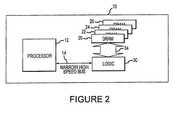
- FIG. 2is a block diagram of a processor-based system that includes a memory system containing stacked memory device dice according to an embodiment of the invention.
- FIG. 3is a timing diagram showing the timing of read data signals shown in FIG. 1 along with read data signal having corrected timing according to an embodiment of the invention.
- FIG. 4is a more detailed block diagram of an embodiment of the processor-based system of FIG. 2 showing the memory system in greater detail.
- FIG. 5is a block diagram showing an embodiment of a timing correction system used in the memory system of FIGS. 2 and 4 .
- FIG. 6is a block diagram showing an embodiment of a strobe timing adjustment circuit used in the timing correction system of FIG. 5 .
- FIG. 7is a block diagram showing an embodiment of a receiver used in the timing correction system of FIG. 5 .
- FIG. 2A computer system including a high-capacity, high bandwidth memory system 10 according to an embodiment of the invention is shown in FIG. 2 .
- the memory system 10is connected to a processor 12 through a relatively narrow high-speed bus 14 that is divided into downstream lanes and separate upstream lanes (not shown in FIG. 2 ).
- the memory system 10includes 4 DRAM dice 20 , 22 , 24 , 26 , which may be identical to each other, stacked on top of each other. Although the memory system 10 includes 4 DRAM dice 20 , 22 , 24 , 26 , other embodiments of the memory device use a greater or lesser number of DRAM dice.
- the stacked DRAM dice 20 , 22 , 24 , 26are connected to a logic die 30 , which serves as the interface with the processor 12 .
- the logic die 30can be physically positioned relative to DRAM dice 20 , 22 , 24 , 26 in any order, such as by stacking the DRAM dice 20 , 22 , 24 , 26 on top of the logic die 30 .
- the logic die 30could, for example, be positioned in the middle of the stack of DRAM dice 20 , 22 , 24 , 26 .
- the logic die 30can implement a variety of functions in the memory system 10 , such as to limit the number of functions that must be implemented in the DRAM dice 20 , 22 , 24 , 26 .
- the logic die 30may perform memory management functions, such as power management and refresh of memory cells in the DRAM dice 20 , 22 , 24 , 26 .
- the logic die 30may perform error checking and correcting (“ECC”) functions.
- ECCerror checking and correcting
- the logic die 30implements the timing correction of signals that the logic die 30 couples to or receives from the DRAM dice 20 , 22 , 24 , 26 , as explained in greater detail below.
- the DRAM dice 20 , 22 , 24 , 26may be connected to each other, and they are connected to the logic die 30 by a relatively wide bus 34 .
- the bus 34may be implemented with through silicon vias (“TSVs”), which comprise a large number of conductors extending at least partially through the DRAM dice 20 , 22 , 24 , 26 at the same locations on the DRAM dice and connect to respective conductors formed on the dice 20 , 22 , 24 , 26 .
- TSVsthrough silicon vias
- each of the DRAM dice 20 , 22 , 24 , 26are divided into 16 autonomous partitions, each of which may contain 2 or 4 independent memory banks.
- each dice 20 , 22 , 24 , 26 that are stacked on top of each othermay be independently accessed for read and write operations.
- Each set of 16 stacked partitionsmay be referred to as a “vault.”
- the memory system 10may contain 16 vaults.
- the logic die 30contains timing correction circuitry for ensuring that read data signals received from the memory device dice 20 , 22 , 24 , 26 are aligned with each other when they are transmitted from the memory system 10 .
- the logic die 30causes the read data signals that would be received from the memory device dice 20 , 22 , 24 , 26 as shown in FIG. 1 so that they are substantially aligned with each other.
- the read data signalsare transmitted from the memory system 10 with a composite eye 28 that is substantially larger than the virtually non-existent composite eye 8 shown in FIG. 1 .
- one of the functions performed by the logic die 30is to serialize the read data bits coupled from the DRAM dice 20 , 22 , 24 , 26 into a serial stream of 16 serial data bits coupled through each of 16 parallel bits of one of the upstream lanes 42 a - d of the bus 14 .
- the logic die 30may perform the functions of deserializing 16 serial data bits coupled through one of the 16-bit downstream lanes 40 a - d of the bus 14 to obtain 256 parallel data bits.
- the logic die 30then couples these 256 bits through one of the 32-bit sub-buses 38 a - p in a serial stream of 8 bits.
- other embodimentsmay use different numbers of lanes 40 , 42 having different widths or different numbers of sub-buses 38 a - p having different widths, and they may couple data bits having different structures.
- the stacking of multiple DRAM diceresults in a memory device having a very large capacity.
- the use of a very wide bus connecting the DRAM diceallows data to be coupled to and from the DRAM dice with a very high bandwidth.
- a logic die 30 according to an embodiment of the inventionis shown in FIG. 4 connected to the processor 12 and the DRAM dice 20 , 22 , 24 , 26 .
- each of the 4 downstream lanes 40 a - dis connected to a respective link interface 50 a - d .
- Each link interface 50 a - dincludes a deserializer 54 that converts each serial stream of 16 data bits on each of the 16-bit lanes 40 a - d to 256 parallel bits. Insofar as there are 4 link interfaces 50 a - d , the link interfaces can together output 1024 output parallel bits.
- Each of the link interfaces 50 a - dapplies its 256 parallel bits to a respective downstream target 60 a - d , which decodes the command and address portions of the received packet and buffers write data in the event a memory request is for a write operation.
- the downstream targets 60 a - doutput their respective commands, addresses and possibly write data to a switch 62 .
- the switch 62contains 16 multiplexers 64 each of which direct the command, addresses and any write data from any of the downstream targets 60 a - d to its respective vault of the DRAM dice 20 , 22 , 24 , 26 .
- each of the downstream targets 60 a - dcan access any of the 16 vaults in the DRAM dice 20 , 22 , 24 , 26 .
- the multiplexers 64use the address in the received memory requests to determine if its respective vault is the target of a memory request.
- Each of the multiplexers 64apply the memory request to a respective one of 16 vault controllers 70 a - p
- Each vault controller 70 a - pincludes a respective memory controller 80 , each of which includes a write buffer 82 , a read buffer 84 and a command pipeline 86 .
- the commands and addresses in memory requests received from the switch 62are loaded into the command pipeline 86 , which subsequently outputs the received commands and corresponding addresses. Any write data in the memory requests are stored in the write buffer 82 .
- the read buffer 84is used to store read data from the respective vault, as will be explained in greater detail below. Both the write data from the write buffer 82 and the commands and addresses from the command pipeline 86 of each of the vault controllers 70 a - p are applied to a memory interface 88 .
- the memory interface 88couples commands and addresses from the command pipelines 86 to the DRAM dice 20 , 22 , 24 , 26 through a command/address bus 94 , and it couples 32-bits of write data from each of the write buffers 82 to the DRAM dice 20 , 22 , 24 , 26 through a 32-bit data bus 92 .
- write dataare loaded into the write buffer 82 as 256 parallel bits, they are output from the buffer 82 in two sets, each set being 128 parallel bits. These 128 bits are then further serialized by the memory interface 88 to 4 sets of 32-bit data, which are coupled through the data bus 92 .
- write dataare coupled to the write buffer 82 in synchronism with a 500 MHz clock so the data are stored in the write buffer at 16 gigabytes (“GB”) per second.
- the write dataare coupled from the write buffer 82 to the DRAM dice 20 , 22 , 24 , 26 using a 2 GHz clock so the data are output from the write buffer 82 at 8 GB/s.
- the write buffers 82will be able to couple the write data to the DRAM dice 20 , 22 , 24 , 26 at least as fast as the data are coupled to the write buffer 82 .
- the command and address for the requestare coupled to the DRAM dice 20 , 22 , 24 , 26 in the same manner as a write request, as explained above.
- 32 bits of read dataare output from the DRAM dice 20 , 22 , 24 , 26 through the 32-bit data bus 92 .
- the memory interface 88deserializes the 32 bits of read data from each of the vaults into two sets of 128-bit read data, which are applied to the read buffer 84 . After 2 sets of 128-bit read data have been stored in the read buffer 84 , the read buffer transmits 256 bits to the switch 62 .
- the switchincludes 4 output multiplexers 104 coupled to respective upstream masters 110 a - d .
- Each multiplexer 104can couple 256 bits of parallel data from any one of the vault controllers 70 a - p to its respective upstream master 110 a - d .
- the upstream masters 110 a - dformat the 256 bits of read data into packet data and couple the packet to respective upstream link interfaces 114 a - d .
- Each of the link interfaces 114 a - dinclude a respective serializer 120 that converts the incoming 256 bits to a serial stream of 16 bits on each bit of a respective one of the 16-bit upstream links 42 a - d.
- the logic die 30corrects the timing of signals that the logic die 30 couples to or receives from the DRAM dice 20 , 22 , 24 , 26 , as explained in greater detail below.
- This timing correctionis implemented by a timing correction system 100 , one of which is included in each of the memory interfaces 88 .
- An embodiment of the timing correction system 100is shown in FIG. 5 .
- the system 100includes a timing control circuit 134 that outputs 4 read data strobe signals RDQS 0 -RDQS 3 .
- the strobe signals RDQS 0 -RDQS 3are in a pattern of alternating high and low logic levels.
- Each of the strobe signals RDQS 0 -RDQS 3is applied to a respective one of 4 strobe timing adjustment circuits 140 a - d , each of which receives a respective timing control signal from the timing control circuit 134 .
- Each of the 4 strobe timing adjustment circuits 140 a - dtransmit respective adjusted read data strobe signals RDQS 0 ′-RDQS 3 ′ to a respective one of the DRAM device dice 20 , 22 , 24 , 26 .
- the strobe timing adjustment circuit 140 atransmits its strobe signal RDQS 0 ′ to the first DRAM device die 20 through a TSV 152 a extending from the logic die 30 to the DRAM device die 20 .
- the strobe signal RDQS 0 ′may also be coupled through additional TSVs 152 b - d extending to the other DRAM device dice 22 , 24 , 26 , but they are not internally connected to any circuitry in the respective DRAM device dice 22 , 24 , 26 .
- the strobe timing adjustment circuit 140 btransmits its strobe signal RDQS 1 ′ to the second DRAM device die 22 through two TSVs 154 a,b
- the strobe timing adjustment circuit 140 ctransmits its strobe signal RDQS 2 ′ to the third DRAM device die 24 through three TSVs 156 a,b,c
- the strobe timing adjustment circuit 140 dtransmits its strobe signal RDQS 3 ′ to the fourth DRAM device die 26 through four TSVs 158 a,b,c,d.
- the respective DRAM device dice 20 , 22 , 24 , 26output 32 bits of read data on a common 32-bit bus 150 .
- Each of the bits of the read datais applied through a respective input buffer 162 to a respective one of 32 receivers 160 (only 1 of which is shown in FIG. 5 ).
- each of the memory interfaces 88 shown in FIG. 4contains 32 receivers 160 .
- Each receiver 160deserializes the received bit of read data into 4 bits of read data.
- the 32 bits of read data collectively received by the 32 receivers 160result in 128 bits of read data.
- a respective transmitter 164is connected to each bit of the bus 150 so that each of the memory interfaces 88 shown in FIG. 4 contains 32 transmitters 164 (only 1 of which is shown in FIG. 5 ).
- Each of the transmitters 164transmits 4 bits of write data through a respective output buffer 166 and serializes the data into 1 bit of write data that is applied to its respective bit of the bus 150 .
- the timing of the read data being transmitted from each of the DRAM device dice 20 , 22 , 24 , 26is controlled by the timing of its respective read data strobe signals RDQS 0 ′-RDQS 3 ′.
- the timing control signals output from the timing control circuit 134cause the respective strobe timing adjustment circuits 140 a - d to properly adjust the timing of the read data strobe signals RDQS 0 ′-RDQS 3 ′ so that the read data is received at the logic die 30 from each of the DRAM device dice 20 , 22 , 24 , 26 with the same timing.
- the receivers 160can capture the read data using the same clock signal CLK regardless of which DRAM device dice 20 , 22 , 24 , 26 transmitted the read data. Therefore, the logic die 30 can transmit the read data from the memory system with the same timing without any additional timing adjustments regardless of which DRAM device dice 20 , 22 , 24 , 26 was the originator of the data.
- a conventional training sequenceis used to determine the correct timing of each of the strobe signals RDQS 0 ′- 3 ′, such as is disclosed in U.S. Pat. No. 6,882,304.
- the timing control circuit 134causes the timing of each of the strobe signals RDQS 0 ′- 3 ′ to be incrementally adjusted while the receivers 160 attempt to capture known read data. The timing that best captures the read data is then used during normal operation. The optimum timing can be determined, for example, by using a timing that is midway between all of the timing values that successfully captured the read data.
- the disclosed embodiment of the memory interface 88uses the timing control circuit 100 only to adjust the timing of the read data.
- a similar timing control circuit 100adjusts the timing of write data signals, command signals and/or address signals in a similar manner.
- the timing control circuitcan vary the timing of these signals transmitted to the DRAM device dice 20 , 22 , 24 , 26 so they are received by the DRAM device dice at the proper time.
- the proper timingcan be determined by conducting a read operations as the timing of these signals are incrementally varied to determine which timing can best be captured in the DRAM device dice 20 , 22 , 24 , 26 .
- the timing control circuit 100is used to apply properly timed read strobe signals to 4 DRAM device dice 20 , 22 , 24 , 26 , other embodiments are used with lesser or additional numbers of DRAM device dice.
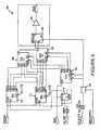
- each of the strobe timing adjustment circuits 140 a - dis shown in FIG. 6 . Although only one timing adjustment circuit 140 is shown in FIG. 6 , it will be understood that 4 of them would be used in the timing control circuit 100 of FIG. 5 .
- the timing adjustment circuit 140receives a respective read data strobe signal RDQS, which consists of alternating high and low logic levels, which may be labeled A-H.
- the RDQS signalis applied to two registers 170 , 172 , each of which has 4 outputs Q 0 -Q 3 .
- the registers 170 , 172are alternately enabled by respective complementary enable signals received from respective outputs of a flip-flop 176 .
- the flip-flop 176is configured to toggle so that it switches states responsive to each rising edge of a clock signal CLK_ 1 XSE.
- the clock signal CLK_ 1 XSEhas a frequency of 500 MHz, so that the flip-flop 176 outputs signal Q high for 4 ns and then output Q* high for 4 ns. Therefore, the flip-flop 176 first enables the register 170 for 4 ns and then enables the register 172 for 4 ns.
- the clock signal CLK_ 1 XSEhas different frequencies. Therefore, the register 170 outputs the signals designated A-D in the read data strobe signal RDQS, and the register 172 outputs the signals designated E-H in the read data strobe signal RDQS.
- the signals output by registers 170 , 172are applied to two multiplexers 180 , 182 . More specifically, the signals designated A, C, E, G from the registers 170 , 172 are applied to respective inputs of the multiplexer 180 , and the signals designated B, D, F, H from the registers 170 , 172 are applied to respective inputs of the multiplexer 182 .
- the multiplexers 180 , 182are controlled by respective select signals to cause one of its inputs to be applied to its output.
- the select signalsare generated by a selector 188 , which may be implemented using a specially configured counter.
- the selector 188is clocked by a clock signal CLK_ 4 X, which, in one embodiment, has a frequency of 1 GHz and is a differential clock signal so that the clock signals have different states. However, the clock signals CLK_ 4 X are coupled through a delay circuit 190 , which may be, for example, a delay line or a phase interpolator. The delay circuit 190 delays the clock signals CLK_ 4 X by an adjustable delay that is controlled by the respective timing control signal from the timing control circuit 134 ( FIG. 5 ). The selector 188 first causes the multiplexer 180 to output the signal A from the register 170 , and it then causes the multiplexer 182 to output the signal B from the register 170 .
- the selector 188then causes the multiplexer 180 to output the signal C from the register 170 , and it then causes the multiplexer 182 to output the signal D from the register 170 .
- the selector 188causes the multiplexer 180 , 182 to sequentially output the signals E-H.
- the respective outputs of the multiplexers 180 , 182are applied to respective inputs of a serializer 194 .
- one of the clock signals CLK_ 4 Xis applied to a clock input of the serializer 194 .
- the clock signalalternately selects each of its inputs and couples them to its output.
- signals designated A,C,E,Gare applied to one input and signals B,D,F,H are applied to the other input, the serializer 194 outputs a signal in the order A,B,C,D,E,F,G,H.
- the serializer 194outputs the original read strobe signal RDQS applied to the registers 170 , 172 except that the timing of the strobe signal RDQS has been adjusted by the timing control signal to generate the timing adjusted read strobe signal RDQS′.
- This RDQS′ signalis transmitted through an output buffer 196 to its respective DRAM device dice 20 , 22 , 24 , 26 , as explained above with reference to FIG. 5 .
- the selector 188 , the multiplexers 180 , 182 and serializer 188together implement a serializing circuit.
- FIG. 7An embodiment of the receiver 160 shown in FIG. 5 is shown in FIG. 7 .
- the receiver 160receives one bit of read data DQ, which, in one embodiment, consists of 8 bits of serial read data, and deserializes it as explained above with reference to FIG. 5 .
- These serial bits of read data DQwill be designated bits A-H for purposes of facilitating an explanation of the receiver 160 .
- the read data bitis applied to the respective data input of 8 flip-flops 200 a - h after being coupled through an input buffer 204 .
- the flip-flops 200 a - hare clocked by a selector 208 , which may be implemented by a counter.
- alternating flip-flops 200 a,c,e,gare clocked by the rising edge of a signal received from the selector 208
- the flip-flops 200 b,d,f,hare clocked by the falling edge of a signal received from the selector 208
- the same signalis applied to adjacent flip flop 200 a,b through 200 g,h.
- each of its outputssequentially transitions high responsive to rising edges of the clock signal CLK_ 2 X, which, in one embodiment, has a frequency of 1 GHz.
- CLK_ 2 Xwhich, in one embodiment, has a frequency of 1 GHz.
- the flip-flop 200 afirst outputs the serial read data bit A, and continues to do so until it is clocked again 4 ns later when the received signal from the selector 208 again transitions high.
- the flip-flop 200 bis clock 1 ns later by the falling edge of the same signal that clocked the flip-flop 200 a , so that the flip-flop 200 b outputs the serial read data bit B for 4 ns.
- the signal applied to the flip-flops 200 a,btransitions low
- the signal applied to the flip-flops 200 c,dtransitions high to cause the flip-flop 200 c to output the serial read data bit C for 4 ns.
- the flip-flops 200 d - gsequentially output read data bits designated D-G.
- all of the serial data bits A-Gwill have been output from the flip-flops 200 a - h.
- the output from each of the first 4 flip flops 200 a - dare applied to a first input of a respective multiplexers 210 a - d
- the output from each of the second 4 flip flops 200 e - hare applied to a second input of the respective multiplexers 210 a - d
- the multiplexers 210 a - dare each controlled by a signal received from a flip-flop 212 , which is configured to toggle responsive to a signal from an AND gate 214 .
- the AND gate 214receives at one of its inputs the clock signal CLK_ 1 XSE which, it may be recalled, has a frequency of 500 MHz in one embodiment.
- the other input of the AND gate 214receives a signal from the output of a flip-flop 216 .
- the flip-flop 216has a data input that receives a signal from the output of a flip-flop 218 .
- the flip-flop 218receives a read enable signal RD_EN at its data input, and it is clocked by the clock signal CLK_ 1 XSE.
- the next rising edge of the clock signal CLK_ 1 XSEcauses the flip-flop 218 to output a high that is applied to the data input of the flip-flop 216 .
- This high output signal from the flip-flop 218is also applied to the enable input of the selector 208 to allow it to begin clocking the flip-flops 200 a - h so that they can collectively output the serial read data bits.
- the flip-flop 216transitions high, thereby causing the output of the AND gate 214 to transition high.
- the flip-flop 212is then clocked, and it continues to be clocked by the clock signal CLK_ 1 XSE until the RD_EN signal transitions low at the end of a read operation. Insofar as the flip-flop 212 is configured to toggle, it outputs a signal that is high for 4 ns and then low for 4 ns. As a result, the multiplexers 210 a - d output serial data bits A-D for 4 ns, and they then output serial data bits E-H for 4 ns. Thus, the 8 ns that it takes to output bits A-H coincides with the 8 ns that the 8 serial data bits A-H are applied to the receiver 160 .
- the timing and frequency exampleshave been provided herein for purposes of explanation, and may be different for other embodiments.
Landscapes
- Engineering & Computer Science (AREA)
- Theoretical Computer Science (AREA)
- Databases & Information Systems (AREA)
- Microelectronics & Electronic Packaging (AREA)
- Computer Hardware Design (AREA)
- Physics & Mathematics (AREA)
- General Engineering & Computer Science (AREA)
- General Physics & Mathematics (AREA)
- Dram (AREA)
Abstract
Description
Claims (20)
Priority Applications (2)
| Application Number | Priority Date | Filing Date | Title |
|---|---|---|---|
| US14/010,159US8793460B2 (en) | 2008-07-21 | 2013-08-26 | Memory system and method using stacked memory device dice, and system using the memory system |
| US14/339,680US9275698B2 (en) | 2008-07-21 | 2014-07-24 | Memory system and method using stacked memory device dice, and system using the memory system |
Applications Claiming Priority (4)
| Application Number | Priority Date | Filing Date | Title |
|---|---|---|---|
| US12/176,951US7855931B2 (en) | 2008-07-21 | 2008-07-21 | Memory system and method using stacked memory device dice, and system using the memory system |
| US12/961,291US8010866B2 (en) | 2008-07-21 | 2010-12-06 | Memory system and method using stacked memory device dice, and system using the memory system |
| US13/209,273US8533416B2 (en) | 2008-07-21 | 2011-08-12 | Memory system and method using stacked memory device dice, and system using the memory system |
| US14/010,159US8793460B2 (en) | 2008-07-21 | 2013-08-26 | Memory system and method using stacked memory device dice, and system using the memory system |
Related Parent Applications (1)
| Application Number | Title | Priority Date | Filing Date |
|---|---|---|---|
| US13/209,273ContinuationUS8533416B2 (en) | 2008-07-21 | 2011-08-12 | Memory system and method using stacked memory device dice, and system using the memory system |
Related Child Applications (1)
| Application Number | Title | Priority Date | Filing Date |
|---|---|---|---|
| US14/339,680ContinuationUS9275698B2 (en) | 2008-07-21 | 2014-07-24 | Memory system and method using stacked memory device dice, and system using the memory system |
Publications (2)
| Publication Number | Publication Date |
|---|---|
| US20130346722A1 US20130346722A1 (en) | 2013-12-26 |
| US8793460B2true US8793460B2 (en) | 2014-07-29 |
Family
ID=41530191
Family Applications (5)
| Application Number | Title | Priority Date | Filing Date |
|---|---|---|---|
| US12/176,951Active2028-12-04US7855931B2 (en) | 2008-07-02 | 2008-07-21 | Memory system and method using stacked memory device dice, and system using the memory system |
| US12/961,291ActiveUS8010866B2 (en) | 2008-07-21 | 2010-12-06 | Memory system and method using stacked memory device dice, and system using the memory system |
| US13/209,273Active2028-12-05US8533416B2 (en) | 2008-07-21 | 2011-08-12 | Memory system and method using stacked memory device dice, and system using the memory system |
| US14/010,159ActiveUS8793460B2 (en) | 2008-07-21 | 2013-08-26 | Memory system and method using stacked memory device dice, and system using the memory system |
| US14/339,680ActiveUS9275698B2 (en) | 2008-07-21 | 2014-07-24 | Memory system and method using stacked memory device dice, and system using the memory system |
Family Applications Before (3)
| Application Number | Title | Priority Date | Filing Date |
|---|---|---|---|
| US12/176,951Active2028-12-04US7855931B2 (en) | 2008-07-02 | 2008-07-21 | Memory system and method using stacked memory device dice, and system using the memory system |
| US12/961,291ActiveUS8010866B2 (en) | 2008-07-21 | 2010-12-06 | Memory system and method using stacked memory device dice, and system using the memory system |
| US13/209,273Active2028-12-05US8533416B2 (en) | 2008-07-21 | 2011-08-12 | Memory system and method using stacked memory device dice, and system using the memory system |
Family Applications After (1)
| Application Number | Title | Priority Date | Filing Date |
|---|---|---|---|
| US14/339,680ActiveUS9275698B2 (en) | 2008-07-21 | 2014-07-24 | Memory system and method using stacked memory device dice, and system using the memory system |
Country Status (7)
| Country | Link |
|---|---|
| US (5) | US7855931B2 (en) |
| EP (1) | EP2319044B1 (en) |
| JP (1) | JP5413690B2 (en) |
| KR (2) | KR101288179B1 (en) |
| CN (1) | CN102099861B (en) |
| TW (1) | TWI426512B (en) |
| WO (1) | WO2010011503A2 (en) |
Cited By (8)
| Publication number | Priority date | Publication date | Assignee | Title |
|---|---|---|---|---|
| US20130019044A1 (en)* | 2011-07-13 | 2013-01-17 | Elpida Memory, Inc. | Semiconductor device |
| US20130058173A1 (en)* | 2011-09-07 | 2013-03-07 | Shuuichi Senou | Semiconductor apparatus |
| US20140337570A1 (en)* | 2008-07-21 | 2014-11-13 | Micron Technology, Inc. | Memory system and method using stacked memory device dice, and system using the memory system |
| US9146811B2 (en) | 2008-07-02 | 2015-09-29 | Micron Technology, Inc. | Method and apparatus for repairing high capacity/high bandwidth memory devices |
| US9411538B2 (en) | 2008-05-29 | 2016-08-09 | Micron Technology, Inc. | Memory systems and methods for controlling the timing of receiving read data |
| US9602080B2 (en) | 2010-12-16 | 2017-03-21 | Micron Technology, Inc. | Phase interpolators and push-pull buffers |
| US10109343B2 (en) | 2008-07-02 | 2018-10-23 | Micron Technology, Inc. | Multi-mode memory device and method having stacked memory dice, a logic die and a command processing circuit and operating in direct and indirect modes |
| US12225705B2 (en) | 2019-02-22 | 2025-02-11 | Semiconductor Energy Laboratory Co., Ltd. | Memory device having error detection function, semiconductor device, and electronic device |
Families Citing this family (90)
| Publication number | Priority date | Publication date | Assignee | Title |
|---|---|---|---|---|
| US9229887B2 (en)* | 2008-02-19 | 2016-01-05 | Micron Technology, Inc. | Memory device with network on chip methods, apparatus, and systems |
| US7979757B2 (en)* | 2008-06-03 | 2011-07-12 | Micron Technology, Inc. | Method and apparatus for testing high capacity/high bandwidth memory devices |
| US7978721B2 (en) | 2008-07-02 | 2011-07-12 | Micron Technology Inc. | Multi-serial interface stacked-die memory architecture |
| US8127204B2 (en) | 2008-08-15 | 2012-02-28 | Micron Technology, Inc. | Memory system and method using a memory device die stacked with a logic die using data encoding, and system using the memory system |
| US8086913B2 (en) | 2008-09-11 | 2011-12-27 | Micron Technology, Inc. | Methods, apparatus, and systems to repair memory |
| US8254191B2 (en) | 2008-10-30 | 2012-08-28 | Micron Technology, Inc. | Switched interface stacked-die memory architecture |
| JP2011081732A (en)* | 2009-10-09 | 2011-04-21 | Elpida Memory Inc | Semiconductor device, adjusting method for the same, and data processing system |
| JP5595708B2 (en)* | 2009-10-09 | 2014-09-24 | ピーエスフォー ルクスコ エスエイアールエル | Semiconductor device, adjustment method thereof, and data processing system |
| US9123552B2 (en) | 2010-03-30 | 2015-09-01 | Micron Technology, Inc. | Apparatuses enabling concurrent communication between an interface die and a plurality of dice stacks, interleaved conductive paths in stacked devices, and methods for forming and operating the same |
| JP2012146377A (en)* | 2011-01-14 | 2012-08-02 | Elpida Memory Inc | Semiconductor device |
| US8554991B2 (en) | 2011-02-09 | 2013-10-08 | Avago Technologies General Ip (Singapore) Pte. Ltd. | High speed interface for dynamic random access memory (DRAM) |
| US9213054B2 (en) | 2011-03-14 | 2015-12-15 | Rambus Inc. | Methods and apparatus for testing inaccessible interface circuits in a semiconductor device |
| US9158546B1 (en) | 2011-04-06 | 2015-10-13 | P4tents1, LLC | Computer program product for fetching from a first physical memory between an execution of a plurality of threads associated with a second physical memory |
| US9164679B2 (en) | 2011-04-06 | 2015-10-20 | Patents1, Llc | System, method and computer program product for multi-thread operation involving first memory of a first memory class and second memory of a second memory class |
| US9176671B1 (en) | 2011-04-06 | 2015-11-03 | P4tents1, LLC | Fetching data between thread execution in a flash/DRAM/embedded DRAM-equipped system |
| US8930647B1 (en) | 2011-04-06 | 2015-01-06 | P4tents1, LLC | Multiple class memory systems |
| US9170744B1 (en) | 2011-04-06 | 2015-10-27 | P4tents1, LLC | Computer program product for controlling a flash/DRAM/embedded DRAM-equipped system |
| US9432298B1 (en) | 2011-12-09 | 2016-08-30 | P4tents1, LLC | System, method, and computer program product for improving memory systems |
| US9417754B2 (en) | 2011-08-05 | 2016-08-16 | P4tents1, LLC | User interface system, method, and computer program product |
| HK1201632A1 (en)* | 2011-11-25 | 2015-09-04 | 考文森智财管理公司 | Memory system and method using stacked memory device dice |
| US8599595B1 (en)* | 2011-12-13 | 2013-12-03 | Michael C. Stephens, Jr. | Memory devices with serially connected signals for stacked arrangements |
| US9472284B2 (en) | 2012-11-19 | 2016-10-18 | Silicon Storage Technology, Inc. | Three-dimensional flash memory system |
| US9417685B2 (en)* | 2013-01-07 | 2016-08-16 | Micron Technology, Inc. | Power management |
| US9679615B2 (en) | 2013-03-15 | 2017-06-13 | Micron Technology, Inc. | Flexible memory system with a controller and a stack of memory |
| JP2016520226A (en)* | 2013-05-16 | 2016-07-11 | アドバンスト・マイクロ・ディバイシズ・インコーポレイテッドAdvanced Micro Devices Incorporated | Memory system with region specific memory access scheduling |
| US9171597B2 (en) | 2013-08-30 | 2015-10-27 | Micron Technology, Inc. | Apparatuses and methods for providing strobe signals to memories |
| US9524013B2 (en)* | 2014-04-16 | 2016-12-20 | International Business Machines Corporation | System interconnect dynamic scaling by lane width and operating frequency balancing |
| KR102192546B1 (en) | 2014-04-22 | 2020-12-18 | 에스케이하이닉스 주식회사 | Semiconductor memory device |
| US9652415B2 (en)* | 2014-07-09 | 2017-05-16 | Sandisk Technologies Llc | Atomic non-volatile memory data transfer |
| US9904621B2 (en) | 2014-07-15 | 2018-02-27 | Sandisk Technologies Llc | Methods and systems for flash buffer sizing |
| US9645744B2 (en) | 2014-07-22 | 2017-05-09 | Sandisk Technologies Llc | Suspending and resuming non-volatile memory operations |
| US9558139B2 (en) | 2014-08-18 | 2017-01-31 | International Business Machines Corporation | System interconnect dynamic scaling handshake using spare bit-lane |
| US9436397B2 (en) | 2014-09-23 | 2016-09-06 | Sandisk Technologies Llc. | Validating the status of memory operations |
| US9330749B1 (en)* | 2014-10-21 | 2016-05-03 | Xilinx, Inc. | Dynamic selection of output delay in a memory control device |
| US9952978B2 (en) | 2014-10-27 | 2018-04-24 | Sandisk Technologies, Llc | Method for improving mixed random performance in low queue depth workloads |
| US9558125B2 (en) | 2014-10-27 | 2017-01-31 | Sandisk Technologies Llc | Processing of un-map commands to enhance performance and endurance of a storage device |
| US9753649B2 (en) | 2014-10-27 | 2017-09-05 | Sandisk Technologies Llc | Tracking intermix of writes and un-map commands across power cycles |
| US9824007B2 (en) | 2014-11-21 | 2017-11-21 | Sandisk Technologies Llc | Data integrity enhancement to protect against returning old versions of data |
| US9817752B2 (en) | 2014-11-21 | 2017-11-14 | Sandisk Technologies Llc | Data integrity enhancement to protect against returning old versions of data |
| US9842633B2 (en)* | 2014-12-11 | 2017-12-12 | Micron Technology, Inc. | Tracking and correction of timing signals |
| US9652430B2 (en)* | 2015-02-10 | 2017-05-16 | Nxp Usa, Inc. | Configurable serial and pulse width modulation interface |
| US9647697B2 (en) | 2015-03-16 | 2017-05-09 | Sandisk Technologies Llc | Method and system for determining soft information offsets |
| KR102373543B1 (en)* | 2015-04-08 | 2022-03-11 | 삼성전자주식회사 | Method and device for controlling operation using temperature deviation in multi-chip package |
| US9652175B2 (en) | 2015-04-09 | 2017-05-16 | Sandisk Technologies Llc | Locally generating and storing RAID stripe parity with single relative memory address for storing data segments and parity in multiple non-volatile memory portions |
| US9864545B2 (en) | 2015-04-14 | 2018-01-09 | Sandisk Technologies Llc | Open erase block read automation |
| US9753653B2 (en) | 2015-04-14 | 2017-09-05 | Sandisk Technologies Llc | High-priority NAND operations management |
| US10372529B2 (en) | 2015-04-20 | 2019-08-06 | Sandisk Technologies Llc | Iterative soft information correction and decoding |
| US9778878B2 (en) | 2015-04-22 | 2017-10-03 | Sandisk Technologies Llc | Method and system for limiting write command execution |
| US9685219B2 (en) | 2015-05-13 | 2017-06-20 | Samsung Electronics Co., Ltd. | Semiconductor memory device for deconcentrating refresh commands and system including the same |
| US9870149B2 (en) | 2015-07-08 | 2018-01-16 | Sandisk Technologies Llc | Scheduling operations in non-volatile memory devices using preference values |
| JP6533576B2 (en)* | 2015-07-13 | 2019-06-19 | 富士フイルム株式会社 | Processing method of pattern structure, manufacturing method of electronic device, and treatment liquid for collapse prevention of pattern structure |
| US9715939B2 (en) | 2015-08-10 | 2017-07-25 | Sandisk Technologies Llc | Low read data storage management |
| US10228990B2 (en) | 2015-11-12 | 2019-03-12 | Sandisk Technologies Llc | Variable-term error metrics adjustment |
| US10126970B2 (en) | 2015-12-11 | 2018-11-13 | Sandisk Technologies Llc | Paired metablocks in non-volatile storage device |
| US9837146B2 (en) | 2016-01-08 | 2017-12-05 | Sandisk Technologies Llc | Memory system temperature management |
| US10732856B2 (en) | 2016-03-03 | 2020-08-04 | Sandisk Technologies Llc | Erase health metric to rank memory portions |
| US10481830B2 (en) | 2016-07-25 | 2019-11-19 | Sandisk Technologies Llc | Selectively throttling host reads for read disturbs in non-volatile memory system |
| US10067689B1 (en)* | 2016-08-29 | 2018-09-04 | Cadence Design Systems, Inc. | Method and apparatus for high bandwidth memory read and write data path training |
| US10381327B2 (en) | 2016-10-06 | 2019-08-13 | Sandisk Technologies Llc | Non-volatile memory system with wide I/O memory die |
| US10042702B2 (en)* | 2016-11-07 | 2018-08-07 | SK Hynix Inc. | Memory device transferring data between master and slave device and semiconductor package including the same |
| KR102681255B1 (en)* | 2017-01-31 | 2024-07-03 | 에스케이하이닉스 주식회사 | Integrated circuit |
| JP6784626B2 (en)* | 2017-03-24 | 2020-11-11 | キヤノン株式会社 | Recording device, control method, and program |
| US10825545B2 (en)* | 2017-04-05 | 2020-11-03 | Micron Technology, Inc. | Memory device loopback systems and methods |
| US10365325B2 (en)* | 2017-08-22 | 2019-07-30 | Micron Technology, Inc. | Semiconductor memory device |
| US10908820B2 (en) | 2017-09-14 | 2021-02-02 | Samsung Electronics Co., Ltd. | Host-based and client-based command scheduling in large bandwidth memory systems |
| US11403241B2 (en) | 2017-10-02 | 2022-08-02 | Micron Technology, Inc. | Communicating data with stacked memory dies |
| US10725913B2 (en)* | 2017-10-02 | 2020-07-28 | Micron Technology, Inc. | Variable modulation scheme for memory device access or operation |
| US10446198B2 (en)* | 2017-10-02 | 2019-10-15 | Micron Technology, Inc. | Multiple concurrent modulation schemes in a memory system |
| US10355893B2 (en)* | 2017-10-02 | 2019-07-16 | Micron Technology, Inc. | Multiplexing distinct signals on a single pin of a memory device |
| JP6395919B1 (en)* | 2017-12-13 | 2018-09-26 | ウィンボンド エレクトロニクス コーポレーション | Semiconductor memory device |
| US11004475B2 (en) | 2018-03-28 | 2021-05-11 | Micron Technology, Inc. | Methods and apparatuses for aligning read data in a stacked semiconductor device |
| KR102639154B1 (en)* | 2018-04-16 | 2024-02-22 | 에스케이하이닉스 주식회사 | Memory device and operation method of the same |
| US10388362B1 (en)* | 2018-05-08 | 2019-08-20 | Micron Technology, Inc. | Half-width, double pumped data path |
| US10782345B2 (en)* | 2018-06-28 | 2020-09-22 | Micron Technology, Inc. | Debugging a semiconductor device |
| US10659215B1 (en)* | 2018-09-19 | 2020-05-19 | Xilinx, Inc. | Training and tracking of DDR memory interface strobe timing |
| TWI682404B (en)* | 2018-10-12 | 2020-01-11 | 新唐科技股份有限公司 | Timing calibration system and method thereof |
| US11079946B2 (en)* | 2018-10-26 | 2021-08-03 | Micron Technology, Inc. | Write training in memory devices |
| US10777232B2 (en)* | 2019-02-04 | 2020-09-15 | Micron Technology, Inc. | High bandwidth memory having plural channels |
| US11194726B2 (en)* | 2019-02-25 | 2021-12-07 | Micron Technology, Inc. | Stacked memory dice for combined access operations |
| WO2020237410A1 (en) | 2019-05-24 | 2020-12-03 | Intel Corporation | Training for chip select signal read operations by memory devices |
| US10991413B2 (en)* | 2019-07-03 | 2021-04-27 | Micron Technology, Inc. | Memory with programmable die refresh stagger |
| US11237734B2 (en)* | 2019-08-19 | 2022-02-01 | Micron Technology, Inc. | High throughput DRAM with distributed column access |
| KR102798952B1 (en)* | 2019-08-21 | 2025-04-21 | 에스케이하이닉스 주식회사 | Semiconductor apparatus and semiconductor system including the same |
| US11442525B2 (en)* | 2019-08-23 | 2022-09-13 | Micron Technology, Inc. | Power management |
| KR102331023B1 (en) | 2020-03-06 | 2021-11-26 | 주식회사 더가든오브내추럴솔루션 | Extract of L. japonica juss leaves and chemical compounds therefrom and cosmetic composition consisting of the same for anti-oxidation and anti-anti-inflammation |
| US11256591B2 (en)* | 2020-06-03 | 2022-02-22 | Western Digital Technologies, Inc. | Die memory operation scheduling plan for power control in an integrated memory assembly |
| US11789893B2 (en)* | 2020-08-05 | 2023-10-17 | Etron Technology, Inc. | Memory system, memory controller and memory chip |
| US12431408B2 (en) | 2022-01-10 | 2025-09-30 | International Business Machines Corporation | TSV and backside power distribution structure |
| WO2024009384A1 (en)* | 2022-07-05 | 2024-01-11 | ウルトラメモリ株式会社 | Semiconductor device |
| US12424264B2 (en)* | 2023-03-14 | 2025-09-23 | Powerchip Semiconductor Manufacturing Corporation | Stacked memory with a timing adjustment function |
Citations (100)
| Publication number | Priority date | Publication date | Assignee | Title |
|---|---|---|---|---|
| US5179303A (en) | 1991-10-24 | 1993-01-12 | Northern Telecom Limited | Signal delay apparatus employing a phase locked loop |
| US5263032A (en) | 1991-06-27 | 1993-11-16 | Digital Equipment Corporation | Computer system operation with corrected read data function |
| US5748914A (en) | 1995-10-19 | 1998-05-05 | Rambus, Inc. | Protocol for communication with dynamic memory |
| US5774475A (en) | 1996-12-05 | 1998-06-30 | National Semiconductor Corporation | Testing scheme that re-uses original stimulus for testing circuitry embedded within a larger circuit |
| US5960008A (en) | 1996-08-30 | 1999-09-28 | Mitsubishi Denki Kabushiki Kaisha | Test circuit |
| US5982684A (en) | 1998-05-28 | 1999-11-09 | Intel Corporation | Parallel access testing of a memory array |
| US6052329A (en) | 1998-01-30 | 2000-04-18 | Mitsubishi Denki Kabushiki Kaisha | Output circuit and synchronous semiconductor memory device having a function of preventing output of invalid data |
| US6177807B1 (en)* | 1999-05-28 | 2001-01-23 | International Business Machines Corporation | High frequency valid data strobe |
| US6181616B1 (en) | 1998-09-03 | 2001-01-30 | Micron Technology, Inc. | Circuits and systems for realigning data output by semiconductor testers to packet-based devices under test |
| US6247138B1 (en) | 1997-06-12 | 2001-06-12 | Fujitsu Limited | Timing signal generating circuit, semiconductor integrated circuit device and semiconductor integrated circuit system to which the timing signal generating circuit is applied, and signal transmission system |
| US6285211B1 (en) | 1997-07-16 | 2001-09-04 | Altera Corporation | I/O buffer circuit with pin multiplexing |
| US20020004893A1 (en) | 2000-01-25 | 2002-01-10 | Nai-Shung Chang | Feedback system for accomodating different memory module loading |
| US6363017B2 (en) | 2000-01-19 | 2002-03-26 | Infineon Technologies Ag | Method and apparatus for alternate operation of a random access memory in single-memory operating mode and in combined multi-memory operating mode |
| US20020054516A1 (en) | 1999-08-31 | 2002-05-09 | Hitachi, Ltd. | Semiconductor device |
| US6401213B1 (en) | 1999-07-09 | 2002-06-04 | Micron Technology, Inc. | Timing circuit for high speed memory |
| US20020097613A1 (en) | 2001-01-19 | 2002-07-25 | Raynham Michael B. | Self-healing memory |
| US20020125933A1 (en) | 1998-06-02 | 2002-09-12 | Fujitsu Limited | Method of and apparatus for correctly transmitting signals at high speed without waveform distortion |
| US20020130687A1 (en) | 2001-03-15 | 2002-09-19 | Kevin Duesman | Antifuse reroute of dies |
| US20020133666A1 (en) | 2001-03-13 | 2002-09-19 | Janzen Jeffery W. | System latency levelization for read data |
| US20020138688A1 (en) | 2001-02-15 | 2002-09-26 | International Business Machines Corporation | Memory array with dual wordline operation |
| US6519194B2 (en) | 2000-01-06 | 2003-02-11 | Mitsubishi Denki Kabushiki Kaisha | Semiconductor memory device with a rapid packet data input, capable of operation check with low speed tester |
| US20030041299A1 (en) | 2001-08-23 | 2003-02-27 | Fujitsu Limited | Memory controller for multilevel cell memory |
| US6574626B1 (en) | 2000-09-29 | 2003-06-03 | Agilent Technologies, Inc. | Method and apparatus for administration of extended memory |
| US20030132790A1 (en) | 2002-01-11 | 2003-07-17 | Brian Amick | Using a push/pull buffer to improve delay locked loop performance |
| US20040073767A1 (en) | 2001-09-28 | 2004-04-15 | Johnson Jerome J. | Memory latency and bandwidth optimizations |
| US20040098545A1 (en) | 2002-11-15 | 2004-05-20 | Pline Steven L. | Transferring data in selectable transfer modes |
| US20040160833A1 (en) | 2003-02-17 | 2004-08-19 | Renesas Technology Corp. | Synchronous semiconductor memory device allowing adjustment of data output timing |
| US20040168101A1 (en) | 2002-04-09 | 2004-08-26 | Atsushi Kubo | Redundant memory system and memory controller used therefor |
| US20040199840A1 (en) | 2001-07-03 | 2004-10-07 | Matsushita Electric Industrial Co., Ltd. | Semiconductor wiring substrate, semiconductor device, method for testing semiconductor device, and method for mounting semiconductor device |
| US20040206982A1 (en) | 2000-09-15 | 2004-10-21 | Lee Thomas H. | Three-dimensional memory device with ECC circuitry |
| US20040237023A1 (en) | 2003-05-20 | 2004-11-25 | Nec Electronics Corporation | Memory device and memory error correction method |
| US20040246026A1 (en) | 2003-06-06 | 2004-12-09 | Microsoft Corporation | Method and apparatus for multi-mode driver |
| US6839260B2 (en) | 2000-01-18 | 2005-01-04 | Hitachi, Ltd. | Semiconductor device having different types of memory cell arrays stacked in a vertical direction |
| US20050005230A1 (en) | 2003-06-30 | 2005-01-06 | Mitsuhiro Koga | Semiconductor integrated circuit device and error checking and correcting method thereof |
| US20050071707A1 (en) | 2003-09-30 | 2005-03-31 | Hampel Craig E. | Integrated circuit with bi-modal data strobe |
| US6882304B2 (en) | 2001-12-21 | 2005-04-19 | Robert Bosch Gmbh | Device for a radar system |
| US20050091471A1 (en) | 2003-10-24 | 2005-04-28 | Microchip Technology Incorporated | Method and system for fast access to stack memory |
| US6889334B1 (en) | 2001-10-02 | 2005-05-03 | Advanced Micro Devices, Inc. | Multimode system for calibrating a data strobe delay for a memory read operation |
| US6907555B1 (en) | 1999-12-17 | 2005-06-14 | Fujitsu Limited | Self-test circuit and memory device incorporating it |
| US20050144546A1 (en) | 2003-12-24 | 2005-06-30 | Fujitsu Limited | Semiconductor integrated circuit and evaluation method of wiring in the same |
| US20050157560A1 (en) | 2002-02-06 | 2005-07-21 | Kabushiki Kaisha Toshiba | Non-volatile semiconductor memory device |
| US20050174877A1 (en) | 2004-02-06 | 2005-08-11 | Soon-Jae Cho | Bus arrangement and method thereof |
| US20050278490A1 (en) | 2004-06-10 | 2005-12-15 | Canon Kabushiki Kaisha | Memory access control apparatus and method of controlling memory access |
| US20050289435A1 (en) | 2004-06-29 | 2005-12-29 | Mulla Dean A | Fast approximate DINV calculation in parallel with coupled ECC generation or correction |
| US20060036827A1 (en) | 2004-07-30 | 2006-02-16 | International Business Machines Corporation | System, method and storage medium for providing segment level sparing |
| US20060059406A1 (en) | 2004-09-10 | 2006-03-16 | Stmicroelectronics S.R.L. | Memory with embedded error correction codes |
| US7058865B2 (en) | 2003-02-26 | 2006-06-06 | Renesas Technology Corp. | Apparatus for testing semiconductor integrated circuit |
| US20060123320A1 (en) | 2004-11-22 | 2006-06-08 | Vogt Pete D | Memory transaction burst operation and memory components supporting temporally multiplexed error correction coding |
| US20060126369A1 (en) | 2004-12-10 | 2006-06-15 | Siva Raghuram | Stacked DRAM memory chip for a dual inline memory module (DIMM) |
| US7107424B1 (en) | 2004-03-25 | 2006-09-12 | Emc Corporation | Memory read strobe pulse optimization training system |
| US20060233012A1 (en) | 2005-03-30 | 2006-10-19 | Elpida Memory, Inc. | Semiconductor storage device having a plurality of stacked memory chips |
| US20060245291A1 (en) | 2005-05-02 | 2006-11-02 | Credence Systems Corporation | Bit synchronization for high-speed serial device testing |
| US20060253723A1 (en) | 2005-05-04 | 2006-11-09 | National Tsing Hua University | Semiconductor memory and method of correcting errors for the same |
| US7135905B2 (en) | 2004-10-12 | 2006-11-14 | Broadcom Corporation | High speed clock and data recovery system |
| US20060262587A1 (en) | 2003-04-21 | 2006-11-23 | Elpida Memory, Inc. | Memory module and memory system |
| US20060273455A1 (en) | 2005-06-01 | 2006-12-07 | Intel Corporation | Electronic packaging including die with through silicon via |
| US7149134B2 (en) | 2002-10-31 | 2006-12-12 | Infineon Technologies Ag | Memory device with column select being variably delayed |
| US7168005B2 (en) | 2000-09-14 | 2007-01-23 | Cadence Design Systems, Inc. | Programable multi-port memory BIST with compact microcode |
| US7171596B2 (en) | 2002-09-11 | 2007-01-30 | Infineon Technologies Ag | Circuit and method for testing embedded DRAM circuits through direct access mode |
| US7184916B2 (en) | 2003-05-20 | 2007-02-27 | Cray Inc. | Apparatus and method for testing memory cards |
| US20070058410A1 (en) | 2005-09-02 | 2007-03-15 | Rajan Suresh N | Methods and apparatus of stacking DRAMs |
| US7197101B2 (en) | 2002-01-02 | 2007-03-27 | Intel Corporation | Phase interpolator based clock recovering |
| US20070070669A1 (en) | 2005-09-26 | 2007-03-29 | Rambus Inc. | Memory module including a plurality of integrated circuit memory devices and a plurality of buffer devices in a matrix topology |
| US20070074093A1 (en) | 2005-09-26 | 2007-03-29 | M-Systems Flash Disk Pioneers Ltd. | NAND flash memory controller exporting and NAND interface |
| US7203259B2 (en) | 2002-01-02 | 2007-04-10 | Intel Corporation | Phase interpolator |
| US20070136645A1 (en) | 2005-12-12 | 2007-06-14 | Mediatek Inc. | Error correction devices and correction methods |
| US7243469B2 (en) | 2001-01-26 | 2007-07-17 | Columbia Insurance Company | Textured laminate flooring |
| US20070271424A1 (en) | 2006-05-16 | 2007-11-22 | Samsung Electronics Co., Ltd. | Memory module, a memory system including a memory controller and a memory module and methods thereof |
| WO2008054696A1 (en) | 2006-10-31 | 2008-05-08 | Advanced Micro Devices, Inc. | Memory controller including a dual- mode memory interconnect |
| US7389375B2 (en) | 2004-07-30 | 2008-06-17 | International Business Machines Corporation | System, method and storage medium for a multi-mode memory buffer device |
| US20080150088A1 (en) | 2006-12-20 | 2008-06-26 | Reed Paul A | Method for incorporating existing silicon die into 3d integrated stack |
| US20080250292A1 (en) | 2007-04-09 | 2008-10-09 | Qimonda Ag | Memory Module with Ranks of Memory Chips |
| US7466179B2 (en) | 2001-02-22 | 2008-12-16 | Realtek Semiconductor Corporation | Phase interpolation circuit |
| US20090006775A1 (en) | 2007-06-27 | 2009-01-01 | Gerald Keith Bartley | Dual-Mode Memory Chip for High Capacity Memory Subsystem |
| US20090016130A1 (en) | 2007-07-12 | 2009-01-15 | Manfred Menke | Memory device and method of testing a memory device |
| US20090021992A1 (en) | 2007-07-18 | 2009-01-22 | Hakjune Oh | Memory with data control |
| US7489743B2 (en) | 2004-07-14 | 2009-02-10 | Samsung Electronics Co., Ltd. | Recovery circuits and methods for the same |
| US20090091968A1 (en) | 2007-10-08 | 2009-04-09 | Stefan Dietrich | Integrated circuit including a memory having a data inversion circuit |
| US7567476B2 (en) | 2005-03-30 | 2009-07-28 | Elpida Memory, Inc. | Semiconductor memory device and testing method thereof |
| US20090196093A1 (en) | 2008-01-31 | 2009-08-06 | Qimonda Ag | Stacked die memory |
| US20090251189A1 (en) | 2008-04-08 | 2009-10-08 | Multi-Phase Phase Interpolator | Multi-Phase Phase Interpolator |
| US20090300314A1 (en) | 2008-05-29 | 2009-12-03 | Micron Technology, Inc. | Memory systems and methods for controlling the timing of receiving read data |
| US20090300444A1 (en) | 2008-06-03 | 2009-12-03 | Micron Technology, Inc. | Method and apparatus for testing high capacity/high bandwidth memory devices |
| US20100005217A1 (en) | 2008-07-02 | 2010-01-07 | Micron Technology, Inc | Multi-mode memory device and method |
| US20100005376A1 (en) | 2008-07-02 | 2010-01-07 | Micron Technology, Inc. | Method and apparatus for repairing high capacity/high bandwidth memory devices |
| US20100014364A1 (en) | 2008-07-21 | 2010-01-21 | Micron Technology, Inc. | Memory system and method using stacked memory device dice, and system using the memory system |
| US20100031129A1 (en) | 2008-08-04 | 2010-02-04 | Micron Technology, Inc. | Multiple device apparatus, systems, and methods |
| US20100042889A1 (en) | 2008-08-15 | 2010-02-18 | Micron Technology, Inc. | Memory system and method using a memory device die stacked with a logic die using data encoding, and system using the memory system |
| US20100070696A1 (en) | 2008-09-17 | 2010-03-18 | Dennis Blankenship | System and Method for Packaged Memory |
| US20100079180A1 (en) | 2008-10-01 | 2010-04-01 | Jin-Gook Kim | Ac-coupling phase interpolator and delay-locked loop using the same |
| US7697369B2 (en) | 2006-06-08 | 2010-04-13 | Elpida Memory, Inc. | System with controller and memory |
| US20100091537A1 (en) | 2006-12-14 | 2010-04-15 | Best Scott C | Multi-die memory device |
| US7710144B2 (en) | 2008-07-01 | 2010-05-04 | International Business Machines Corporation | Controlling for variable impedance and voltage in a memory system |
| US20100110748A1 (en) | 2007-04-17 | 2010-05-06 | Best Scott C | Hybrid volatile and non-volatile memory device |
| US7764564B2 (en) | 2006-12-04 | 2010-07-27 | Nec Corporation | Semiconductor device |
| US7772907B2 (en) | 2007-10-22 | 2010-08-10 | Samsung Electronics Co., Ltd. | Linear digital phase interpolator and semi-digital delay locked loop (DLL) |
| WO2012060097A1 (en) | 2010-11-02 | 2012-05-10 | 日本電気株式会社 | Memory module and memory system |
| US20120155142A1 (en) | 2010-12-16 | 2012-06-21 | Micron Technology, Inc. | Phase interpolators and push-pull buffers |
| US8248138B2 (en) | 2009-03-10 | 2012-08-21 | Realtek Semiconductor Corp. | Method and apparatus for preventing phase interpolation circuit from glitch during clock switching |
| US8356138B1 (en) | 2007-08-20 | 2013-01-15 | Xilinx, Inc. | Methods for implementing programmable memory controller for distributed DRAM system-in-package (SiP) |
Family Cites Families (39)
| Publication number | Priority date | Publication date | Assignee | Title |
|---|---|---|---|---|
| JPH05265872A (en) | 1992-03-17 | 1993-10-15 | Fujitsu Ltd | Access control circuit |
| US6551857B2 (en) | 1997-04-04 | 2003-04-22 | Elm Technology Corporation | Three dimensional structure integrated circuits |
| US6191999B1 (en)* | 1997-06-20 | 2001-02-20 | Fujitsu Limited | Semiconductor memory device with reduced power consumption |
| JP3270367B2 (en) | 1997-09-29 | 2002-04-02 | エヌイーシーフィールディング株式会社 | Semiconductor storage device |
| JP4342654B2 (en) | 1999-10-12 | 2009-10-14 | 富士通マイクロエレクトロニクス株式会社 | Delay circuit and semiconductor integrated circuit |
| TW466394B (en)* | 2000-01-04 | 2001-12-01 | Via Tech Inc | Terminated circuit module and computer system using the same |
| US6329859B1 (en) | 2000-03-23 | 2001-12-11 | Bitblitz Communications, Inc. | N-way circular phase interpolator for generating a signal having arbitrary phase |
| JP4056213B2 (en) | 2000-11-06 | 2008-03-05 | 日本電気株式会社 | Phase difference signal generation circuit, and multiphase clock generation circuit and integrated circuit using the same |
| US7039121B2 (en) | 2000-11-22 | 2006-05-02 | Silicon Image | Method and system for transition-controlled selective block inversion communications |
| JP4627411B2 (en) | 2003-05-20 | 2011-02-09 | ルネサスエレクトロニクス株式会社 | Memory device and memory error correction method |
| TWI252494B (en) | 2003-06-11 | 2006-04-01 | Samsung Electronics Co Ltd | Memory system with reduced pin count |
| JP2005033958A (en) | 2003-07-10 | 2005-02-03 | Fuji Electric Fa Components & Systems Co Ltd | DC motor speed control device |
| US7323917B2 (en) | 2003-09-15 | 2008-01-29 | Texas Instruments Incorporated | Method and apparatus for synthesizing a clock signal having a frequency near the frequency of a source clock signal |
| US7009872B2 (en) | 2003-12-22 | 2006-03-07 | Hewlett-Packard Development Company, L.P. | MRAM storage device |
| US7243489B2 (en) | 2004-01-13 | 2007-07-17 | Arvin Technologies, Inc. | Method and apparatus for monitoring engine performance as a function of soot accumulation in a filter |
| JP4451189B2 (en) | 2004-04-05 | 2010-04-14 | 株式会社アドバンテスト | Test apparatus, phase adjustment method, and memory controller |
| GB0413071D0 (en) | 2004-06-12 | 2004-07-14 | Texas Instruments Ltd | Triangulating phase interpolator |
| US7330370B2 (en) | 2004-07-20 | 2008-02-12 | Unity Semiconductor Corporation | Enhanced functionality in a two-terminal memory array |
| JP4444770B2 (en) | 2004-09-14 | 2010-03-31 | シャープ株式会社 | Memory device |
| US20060223012A1 (en) | 2005-03-30 | 2006-10-05 | Konica Minolta Medical & Graphic, Inc. | Thermal processing method of silver salt photothermographic dry imaging material |
| US7205811B2 (en) | 2005-03-31 | 2007-04-17 | Agere Systems Inc. | Methods and apparatus for maintaining desired slope of clock edges in a phase interpolator using an adjustable bias |
| US7562271B2 (en) | 2005-09-26 | 2009-07-14 | Rambus Inc. | Memory system topologies including a buffer device and an integrated circuit memory device |
| JP4790386B2 (en) | 2005-11-18 | 2011-10-12 | エルピーダメモリ株式会社 | Stacked memory |
| US20070153951A1 (en) | 2005-12-29 | 2007-07-05 | Lim Chee H | Phase interpolation for phase-locked loops |
| WO2007095080A2 (en)* | 2006-02-09 | 2007-08-23 | Metaram, Inc. | Memory circuit system and method |
| JP4828251B2 (en) | 2006-02-22 | 2011-11-30 | エルピーダメモリ株式会社 | Stacked semiconductor memory device and control method thereof |
| EP2487794A3 (en) | 2006-08-22 | 2013-02-13 | Mosaid Technologies Incorporated | Modular command structure for memory and memory system |
| JP4245180B2 (en) | 2006-10-30 | 2009-03-25 | エルピーダメモリ株式会社 | Stacked memory |
| US8737451B2 (en) | 2007-03-09 | 2014-05-27 | Qualcomm Incorporated | MMSE MUD in 1x mobiles |
| US20080270842A1 (en) | 2007-04-26 | 2008-10-30 | Jenchang Ho | Computer operating system handling of severe hardware errors |
| EP2166719A4 (en) | 2007-06-08 | 2014-04-16 | Nec Corp | Modulation device and pulse wave generation device |
| WO2009055103A2 (en) | 2007-10-22 | 2009-04-30 | Rambus, Inc. | Low-power source-synchronous signaling |
| US8175207B2 (en) | 2007-12-12 | 2012-05-08 | Applied Micro Circuits Corporation | ISI pattern-weighted early-late phase detector with jitter correction |
| US7924637B2 (en) | 2008-03-31 | 2011-04-12 | Advanced Micro Devices, Inc. | Method for training dynamic random access memory (DRAM) controller timing delays |
| KR20100072704A (en) | 2008-12-22 | 2010-07-01 | 삼성전자주식회사 | Delay locked loop circuit controlled by column address strobe write latency |
| US8063683B2 (en) | 2009-06-08 | 2011-11-22 | Integrated Device Technology, Inc. | Low power clock and data recovery phase interpolator |
| US8258837B2 (en) | 2009-12-17 | 2012-09-04 | Intel Corporation | Controlled clock phase generation |
| KR101079209B1 (en) | 2010-04-28 | 2011-11-03 | 주식회사 하이닉스반도체 | Device for transmitting and receiving data in semiconductor system |
| US9171597B2 (en) | 2013-08-30 | 2015-10-27 | Micron Technology, Inc. | Apparatuses and methods for providing strobe signals to memories |
- 2008
- 2008-07-21USUS12/176,951patent/US7855931B2/enactiveActive
- 2009
- 2009-07-09WOPCT/US2009/050155patent/WO2010011503A2/enactiveApplication Filing
- 2009-07-09KRKR1020117001535Apatent/KR101288179B1/enactiveActive
- 2009-07-09CNCN200980128341.4Apatent/CN102099861B/enactiveActive
- 2009-07-09JPJP2011520079Apatent/JP5413690B2/enactiveActive
- 2009-07-09KRKR1020137010171Apatent/KR101364348B1/enactiveActive
- 2009-07-09EPEP09800787.5Apatent/EP2319044B1/enactiveActive
- 2009-07-21TWTW098124606Apatent/TWI426512B/enactive
- 2010
- 2010-12-06USUS12/961,291patent/US8010866B2/enactiveActive
- 2011
- 2011-08-12USUS13/209,273patent/US8533416B2/enactiveActive
- 2013
- 2013-08-26USUS14/010,159patent/US8793460B2/enactiveActive
- 2014
- 2014-07-24USUS14/339,680patent/US9275698B2/enactiveActive
Patent Citations (122)
| Publication number | Priority date | Publication date | Assignee | Title |
|---|---|---|---|---|
| US5263032A (en) | 1991-06-27 | 1993-11-16 | Digital Equipment Corporation | Computer system operation with corrected read data function |
| US5179303A (en) | 1991-10-24 | 1993-01-12 | Northern Telecom Limited | Signal delay apparatus employing a phase locked loop |
| US5748914A (en) | 1995-10-19 | 1998-05-05 | Rambus, Inc. | Protocol for communication with dynamic memory |
| US6122688A (en) | 1995-10-19 | 2000-09-19 | Rambus Inc. | Protocol for communication with dynamic memory |
| US5960008A (en) | 1996-08-30 | 1999-09-28 | Mitsubishi Denki Kabushiki Kaisha | Test circuit |
| US5774475A (en) | 1996-12-05 | 1998-06-30 | National Semiconductor Corporation | Testing scheme that re-uses original stimulus for testing circuitry embedded within a larger circuit |
| US6247138B1 (en) | 1997-06-12 | 2001-06-12 | Fujitsu Limited | Timing signal generating circuit, semiconductor integrated circuit device and semiconductor integrated circuit system to which the timing signal generating circuit is applied, and signal transmission system |
| US6285211B1 (en) | 1997-07-16 | 2001-09-04 | Altera Corporation | I/O buffer circuit with pin multiplexing |
| US6052329A (en) | 1998-01-30 | 2000-04-18 | Mitsubishi Denki Kabushiki Kaisha | Output circuit and synchronous semiconductor memory device having a function of preventing output of invalid data |
| US5982684A (en) | 1998-05-28 | 1999-11-09 | Intel Corporation | Parallel access testing of a memory array |
| US20020125933A1 (en) | 1998-06-02 | 2002-09-12 | Fujitsu Limited | Method of and apparatus for correctly transmitting signals at high speed without waveform distortion |
| US6181616B1 (en) | 1998-09-03 | 2001-01-30 | Micron Technology, Inc. | Circuits and systems for realigning data output by semiconductor testers to packet-based devices under test |
| US6177807B1 (en)* | 1999-05-28 | 2001-01-23 | International Business Machines Corporation | High frequency valid data strobe |
| US6401213B1 (en) | 1999-07-09 | 2002-06-04 | Micron Technology, Inc. | Timing circuit for high speed memory |
| US20020054516A1 (en) | 1999-08-31 | 2002-05-09 | Hitachi, Ltd. | Semiconductor device |
| US6907555B1 (en) | 1999-12-17 | 2005-06-14 | Fujitsu Limited | Self-test circuit and memory device incorporating it |
| US6519194B2 (en) | 2000-01-06 | 2003-02-11 | Mitsubishi Denki Kabushiki Kaisha | Semiconductor memory device with a rapid packet data input, capable of operation check with low speed tester |
| US6839260B2 (en) | 2000-01-18 | 2005-01-04 | Hitachi, Ltd. | Semiconductor device having different types of memory cell arrays stacked in a vertical direction |
| US6363017B2 (en) | 2000-01-19 | 2002-03-26 | Infineon Technologies Ag | Method and apparatus for alternate operation of a random access memory in single-memory operating mode and in combined multi-memory operating mode |
| US20020004893A1 (en) | 2000-01-25 | 2002-01-10 | Nai-Shung Chang | Feedback system for accomodating different memory module loading |
| US7168005B2 (en) | 2000-09-14 | 2007-01-23 | Cadence Design Systems, Inc. | Programable multi-port memory BIST with compact microcode |
| US20040206982A1 (en) | 2000-09-15 | 2004-10-21 | Lee Thomas H. | Three-dimensional memory device with ECC circuitry |
| US6574626B1 (en) | 2000-09-29 | 2003-06-03 | Agilent Technologies, Inc. | Method and apparatus for administration of extended memory |
| US20020097613A1 (en) | 2001-01-19 | 2002-07-25 | Raynham Michael B. | Self-healing memory |
| US7243469B2 (en) | 2001-01-26 | 2007-07-17 | Columbia Insurance Company | Textured laminate flooring |
| US20020138688A1 (en) | 2001-02-15 | 2002-09-26 | International Business Machines Corporation | Memory array with dual wordline operation |
| US7466179B2 (en) | 2001-02-22 | 2008-12-16 | Realtek Semiconductor Corporation | Phase interpolation circuit |
| US20020133666A1 (en) | 2001-03-13 | 2002-09-19 | Janzen Jeffery W. | System latency levelization for read data |
| US6658523B2 (en) | 2001-03-13 | 2003-12-02 | Micron Technology, Inc. | System latency levelization for read data |
| US20020130687A1 (en) | 2001-03-15 | 2002-09-19 | Kevin Duesman | Antifuse reroute of dies |
| US20040199840A1 (en) | 2001-07-03 | 2004-10-07 | Matsushita Electric Industrial Co., Ltd. | Semiconductor wiring substrate, semiconductor device, method for testing semiconductor device, and method for mounting semiconductor device |
| US20030041299A1 (en) | 2001-08-23 | 2003-02-27 | Fujitsu Limited | Memory controller for multilevel cell memory |
| US20040073767A1 (en) | 2001-09-28 | 2004-04-15 | Johnson Jerome J. | Memory latency and bandwidth optimizations |
| US6889334B1 (en) | 2001-10-02 | 2005-05-03 | Advanced Micro Devices, Inc. | Multimode system for calibrating a data strobe delay for a memory read operation |
| US6882304B2 (en) | 2001-12-21 | 2005-04-19 | Robert Bosch Gmbh | Device for a radar system |
| US7197101B2 (en) | 2002-01-02 | 2007-03-27 | Intel Corporation | Phase interpolator based clock recovering |
| US7203259B2 (en) | 2002-01-02 | 2007-04-10 | Intel Corporation | Phase interpolator |
| US20030132790A1 (en) | 2002-01-11 | 2003-07-17 | Brian Amick | Using a push/pull buffer to improve delay locked loop performance |
| US6650157B2 (en) | 2002-01-11 | 2003-11-18 | Sun Microsystems, Inc. | Using a push/pull buffer to improve delay locked loop performance |
| US20050157560A1 (en) | 2002-02-06 | 2005-07-21 | Kabushiki Kaisha Toshiba | Non-volatile semiconductor memory device |
| US20040168101A1 (en) | 2002-04-09 | 2004-08-26 | Atsushi Kubo | Redundant memory system and memory controller used therefor |
| US7171596B2 (en) | 2002-09-11 | 2007-01-30 | Infineon Technologies Ag | Circuit and method for testing embedded DRAM circuits through direct access mode |
| US7149134B2 (en) | 2002-10-31 | 2006-12-12 | Infineon Technologies Ag | Memory device with column select being variably delayed |
| US20040098545A1 (en) | 2002-11-15 | 2004-05-20 | Pline Steven L. | Transferring data in selectable transfer modes |
| US20040160833A1 (en) | 2003-02-17 | 2004-08-19 | Renesas Technology Corp. | Synchronous semiconductor memory device allowing adjustment of data output timing |
| US7058865B2 (en) | 2003-02-26 | 2006-06-06 | Renesas Technology Corp. | Apparatus for testing semiconductor integrated circuit |
| US20060262587A1 (en) | 2003-04-21 | 2006-11-23 | Elpida Memory, Inc. | Memory module and memory system |
| US20040237023A1 (en) | 2003-05-20 | 2004-11-25 | Nec Electronics Corporation | Memory device and memory error correction method |
| US7184916B2 (en) | 2003-05-20 | 2007-02-27 | Cray Inc. | Apparatus and method for testing memory cards |
| US20040246026A1 (en) | 2003-06-06 | 2004-12-09 | Microsoft Corporation | Method and apparatus for multi-mode driver |
| US20050005230A1 (en) | 2003-06-30 | 2005-01-06 | Mitsuhiro Koga | Semiconductor integrated circuit device and error checking and correcting method thereof |
| US20050071707A1 (en) | 2003-09-30 | 2005-03-31 | Hampel Craig E. | Integrated circuit with bi-modal data strobe |
| WO2005033958A1 (en) | 2003-09-30 | 2005-04-14 | Rambus Inc. | Integrated circuit with bi-modal data strobe |
| US20050091471A1 (en) | 2003-10-24 | 2005-04-28 | Microchip Technology Incorporated | Method and system for fast access to stack memory |
| US20050144546A1 (en) | 2003-12-24 | 2005-06-30 | Fujitsu Limited | Semiconductor integrated circuit and evaluation method of wiring in the same |
| US20050174877A1 (en) | 2004-02-06 | 2005-08-11 | Soon-Jae Cho | Bus arrangement and method thereof |
| US7107424B1 (en) | 2004-03-25 | 2006-09-12 | Emc Corporation | Memory read strobe pulse optimization training system |
| US20050278490A1 (en) | 2004-06-10 | 2005-12-15 | Canon Kabushiki Kaisha | Memory access control apparatus and method of controlling memory access |
| US20050289435A1 (en) | 2004-06-29 | 2005-12-29 | Mulla Dean A | Fast approximate DINV calculation in parallel with coupled ECC generation or correction |
| US7489743B2 (en) | 2004-07-14 | 2009-02-10 | Samsung Electronics Co., Ltd. | Recovery circuits and methods for the same |
| US20060036827A1 (en) | 2004-07-30 | 2006-02-16 | International Business Machines Corporation | System, method and storage medium for providing segment level sparing |
| US7389375B2 (en) | 2004-07-30 | 2008-06-17 | International Business Machines Corporation | System, method and storage medium for a multi-mode memory buffer device |
| US20060059406A1 (en) | 2004-09-10 | 2006-03-16 | Stmicroelectronics S.R.L. | Memory with embedded error correction codes |
| US7135905B2 (en) | 2004-10-12 | 2006-11-14 | Broadcom Corporation | High speed clock and data recovery system |
| US20060123320A1 (en) | 2004-11-22 | 2006-06-08 | Vogt Pete D | Memory transaction burst operation and memory components supporting temporally multiplexed error correction coding |
| CN101036131A (en) | 2004-11-22 | 2007-09-12 | 英特尔公司 | Memory transaction burst operation and memory components supporting temporally multiplexed error correction coding |
| US7464241B2 (en) | 2004-11-22 | 2008-12-09 | Intel Corporation | Memory transaction burst operation and memory components supporting temporally multiplexed error correction coding |
| US20060126369A1 (en) | 2004-12-10 | 2006-06-15 | Siva Raghuram | Stacked DRAM memory chip for a dual inline memory module (DIMM) |
| US7567476B2 (en) | 2005-03-30 | 2009-07-28 | Elpida Memory, Inc. | Semiconductor memory device and testing method thereof |
| US20060233012A1 (en) | 2005-03-30 | 2006-10-19 | Elpida Memory, Inc. | Semiconductor storage device having a plurality of stacked memory chips |
| US20060245291A1 (en) | 2005-05-02 | 2006-11-02 | Credence Systems Corporation | Bit synchronization for high-speed serial device testing |
| US20060253723A1 (en) | 2005-05-04 | 2006-11-09 | National Tsing Hua University | Semiconductor memory and method of correcting errors for the same |
| US20060273455A1 (en) | 2005-06-01 | 2006-12-07 | Intel Corporation | Electronic packaging including die with through silicon via |
| US20070058410A1 (en) | 2005-09-02 | 2007-03-15 | Rajan Suresh N | Methods and apparatus of stacking DRAMs |
| US20070070669A1 (en) | 2005-09-26 | 2007-03-29 | Rambus Inc. | Memory module including a plurality of integrated circuit memory devices and a plurality of buffer devices in a matrix topology |
| US20070074093A1 (en) | 2005-09-26 | 2007-03-29 | M-Systems Flash Disk Pioneers Ltd. | NAND flash memory controller exporting and NAND interface |
| US20070136645A1 (en) | 2005-12-12 | 2007-06-14 | Mediatek Inc. | Error correction devices and correction methods |
| US20070271424A1 (en) | 2006-05-16 | 2007-11-22 | Samsung Electronics Co., Ltd. | Memory module, a memory system including a memory controller and a memory module and methods thereof |
| US7697369B2 (en) | 2006-06-08 | 2010-04-13 | Elpida Memory, Inc. | System with controller and memory |
| US20080147897A1 (en) | 2006-10-31 | 2008-06-19 | Advanced Micro Devices, Inc. | Memory controller including a dual-mode memory interconnect |
| WO2008054696A1 (en) | 2006-10-31 | 2008-05-08 | Advanced Micro Devices, Inc. | Memory controller including a dual- mode memory interconnect |
| US7764564B2 (en) | 2006-12-04 | 2010-07-27 | Nec Corporation | Semiconductor device |
| US20100091537A1 (en) | 2006-12-14 | 2010-04-15 | Best Scott C | Multi-die memory device |
| US20080150088A1 (en) | 2006-12-20 | 2008-06-26 | Reed Paul A | Method for incorporating existing silicon die into 3d integrated stack |
| US20080250292A1 (en) | 2007-04-09 | 2008-10-09 | Qimonda Ag | Memory Module with Ranks of Memory Chips |
| US20100110748A1 (en) | 2007-04-17 | 2010-05-06 | Best Scott C | Hybrid volatile and non-volatile memory device |
| US20090006775A1 (en) | 2007-06-27 | 2009-01-01 | Gerald Keith Bartley | Dual-Mode Memory Chip for High Capacity Memory Subsystem |
| US20090016130A1 (en) | 2007-07-12 | 2009-01-15 | Manfred Menke | Memory device and method of testing a memory device |
| US20090021992A1 (en) | 2007-07-18 | 2009-01-22 | Hakjune Oh | Memory with data control |
| US8356138B1 (en) | 2007-08-20 | 2013-01-15 | Xilinx, Inc. | Methods for implementing programmable memory controller for distributed DRAM system-in-package (SiP) |
| US20090091968A1 (en) | 2007-10-08 | 2009-04-09 | Stefan Dietrich | Integrated circuit including a memory having a data inversion circuit |
| US7772907B2 (en) | 2007-10-22 | 2010-08-10 | Samsung Electronics Co., Ltd. | Linear digital phase interpolator and semi-digital delay locked loop (DLL) |
| US20090196093A1 (en) | 2008-01-31 | 2009-08-06 | Qimonda Ag | Stacked die memory |
| US20090251189A1 (en) | 2008-04-08 | 2009-10-08 | Multi-Phase Phase Interpolator | Multi-Phase Phase Interpolator |
| US20130318298A1 (en) | 2008-05-29 | 2013-11-28 | Micron Technology, Inc. | Memory systems and methods for controlling the timing of receiving read data |
| US20090300314A1 (en) | 2008-05-29 | 2009-12-03 | Micron Technology, Inc. | Memory systems and methods for controlling the timing of receiving read data |
| US20110271158A1 (en) | 2008-06-03 | 2011-11-03 | Micron Technology, Inc. | Method and apparatus for testing high capacity/high bandwidth memory devices |
| US7979757B2 (en) | 2008-06-03 | 2011-07-12 | Micron Technology, Inc. | Method and apparatus for testing high capacity/high bandwidth memory devices |
| US20090300444A1 (en) | 2008-06-03 | 2009-12-03 | Micron Technology, Inc. | Method and apparatus for testing high capacity/high bandwidth memory devices |
| US7710144B2 (en) | 2008-07-01 | 2010-05-04 | International Business Machines Corporation | Controlling for variable impedance and voltage in a memory system |
| WO2010002561A2 (en) | 2008-07-02 | 2010-01-07 | Micron Technology, Inc. | Method and apparatus for repairing high capacity/high bandwidth memory devices |
| US8289760B2 (en) | 2008-07-02 | 2012-10-16 | Micron Technology, Inc. | Multi-mode memory device and method having stacked memory dice, a logic die and a command processing circuit and operating in direct and indirect modes |
| US20100005217A1 (en) | 2008-07-02 | 2010-01-07 | Micron Technology, Inc | Multi-mode memory device and method |
| US20100005376A1 (en) | 2008-07-02 | 2010-01-07 | Micron Technology, Inc. | Method and apparatus for repairing high capacity/high bandwidth memory devices |
| US20110075497A1 (en) | 2008-07-21 | 2011-03-31 | Micron Technology, Inc. | Memory system and method using stacked memory device dice, and system using the memory system |
| US7855931B2 (en) | 2008-07-21 | 2010-12-21 | Micron Technology, Inc. | Memory system and method using stacked memory device dice, and system using the memory system |
| WO2010011503A2 (en) | 2008-07-21 | 2010-01-28 | Micron Technology, Inc. | Memory system and method using stacked memory device dice, and system using the memory system |
| US8010866B2 (en) | 2008-07-21 | 2011-08-30 | Micron Technology, Inc. | Memory system and method using stacked memory device dice, and system using the memory system |
| US20100014364A1 (en) | 2008-07-21 | 2010-01-21 | Micron Technology, Inc. | Memory system and method using stacked memory device dice, and system using the memory system |
| US20110296227A1 (en) | 2008-07-21 | 2011-12-01 | Micron Technology, Inc. | Memory system and method using stacked memory device dice, and system using the memory system |
| US20100031129A1 (en) | 2008-08-04 | 2010-02-04 | Micron Technology, Inc. | Multiple device apparatus, systems, and methods |
| US20120144276A1 (en) | 2008-08-15 | 2012-06-07 | Micron Technology, Inc. | Memory system and method using a memory device die stacked with a logic die using data encoding, and system using the memory system |
| US8127204B2 (en) | 2008-08-15 | 2012-02-28 | Micron Technology, Inc. | Memory system and method using a memory device die stacked with a logic die using data encoding, and system using the memory system |
| US20100042889A1 (en) | 2008-08-15 | 2010-02-18 | Micron Technology, Inc. | Memory system and method using a memory device die stacked with a logic die using data encoding, and system using the memory system |
| US20140053040A1 (en) | 2008-08-15 | 2014-02-20 | Micron Technology, Inc. | Memory system and method using a memory device die stacked with a logic die using data encoding, and system using the memory system |
| US20100070696A1 (en) | 2008-09-17 | 2010-03-18 | Dennis Blankenship | System and Method for Packaged Memory |
| US20100079180A1 (en) | 2008-10-01 | 2010-04-01 | Jin-Gook Kim | Ac-coupling phase interpolator and delay-locked loop using the same |
| US8248138B2 (en) | 2009-03-10 | 2012-08-21 | Realtek Semiconductor Corp. | Method and apparatus for preventing phase interpolation circuit from glitch during clock switching |
| WO2012060097A1 (en) | 2010-11-02 | 2012-05-10 | 日本電気株式会社 | Memory module and memory system |
| US20120155142A1 (en) | 2010-12-16 | 2012-06-21 | Micron Technology, Inc. | Phase interpolators and push-pull buffers |
| US8400808B2 (en) | 2010-12-16 | 2013-03-19 | Micron Technology, Inc. | Phase interpolators and push-pull buffers |
| US20130208549A1 (en) | 2010-12-16 | 2013-08-15 | Micron Technology, Inc. | Phase interpolators and push-pull buffers |
Non-Patent Citations (11)
| Title |
|---|
| CN First Office Action for Appl No. 200980128341.4, Apr. 3, 2013. |
| Extended European Search Report dated Aug. 2, 2011 for European Patent Application No. 09800787.5. |
| International Search Report and Written Opinion dated Feb. 11, 2010 for International Application No. PCT/US2009/050155. |
| LaBerge, et al., First examination report received for EP 09800787.5 dated Feb. 21, 2013. |
| Non-Final Office Action for Appl No. 10-2013-7010171, Jun. 14, 2013. |
| Notice of Final Rejection dated Feb. 2, 2013 for KR Appl. No. 10-2011-7001535. |
| Notice of Preliminary Rejection dated Jun. 18, 2012 for KR Appl. No. 10-2011-7001535. |
| Notice of Rejection for Appl No. 2011-520079 dated Jun. 25, 2013. |
| Office Action received for JP Appln No. 2011-520079 dated Feb. 12, 2013. |
| Second Office Action issued by State Intellectual Property Office for CN Appl No. 200980128341.4; Issued Nov. 19, 2013. |
| TW Office Action for Appl No. 098124606, May 9, 2013. |
Cited By (13)
| Publication number | Priority date | Publication date | Assignee | Title |
|---|---|---|---|---|
| US9411538B2 (en) | 2008-05-29 | 2016-08-09 | Micron Technology, Inc. | Memory systems and methods for controlling the timing of receiving read data |
| US10892003B2 (en) | 2008-07-02 | 2021-01-12 | Micron Technology, Inc. | Multi-mode memory device and method having stacked memory dice, a logic die and a command processing circuit and operating in direct and indirect modes |
| US10109343B2 (en) | 2008-07-02 | 2018-10-23 | Micron Technology, Inc. | Multi-mode memory device and method having stacked memory dice, a logic die and a command processing circuit and operating in direct and indirect modes |
| US9146811B2 (en) | 2008-07-02 | 2015-09-29 | Micron Technology, Inc. | Method and apparatus for repairing high capacity/high bandwidth memory devices |
| US9275698B2 (en)* | 2008-07-21 | 2016-03-01 | Micron Technology, Inc. | Memory system and method using stacked memory device dice, and system using the memory system |
| US20140337570A1 (en)* | 2008-07-21 | 2014-11-13 | Micron Technology, Inc. | Memory system and method using stacked memory device dice, and system using the memory system |
| US9602080B2 (en) | 2010-12-16 | 2017-03-21 | Micron Technology, Inc. | Phase interpolators and push-pull buffers |
| US9899994B2 (en) | 2010-12-16 | 2018-02-20 | Micron Technology, Inc. | Phase interpolators and push-pull buffers |
| US20130019044A1 (en)* | 2011-07-13 | 2013-01-17 | Elpida Memory, Inc. | Semiconductor device |
| US9152594B2 (en)* | 2011-07-13 | 2015-10-06 | Ps4 Luxco S.A.R.L. | Semiconductor memory device for high speed reading and writing |
| US9202541B2 (en)* | 2011-09-07 | 2015-12-01 | Renesas Electronics Corporation | Semiconductor apparatus configured to reduce data processing performance |
| US20130058173A1 (en)* | 2011-09-07 | 2013-03-07 | Shuuichi Senou | Semiconductor apparatus |
| US12225705B2 (en) | 2019-02-22 | 2025-02-11 | Semiconductor Energy Laboratory Co., Ltd. | Memory device having error detection function, semiconductor device, and electronic device |
Also Published As
| Publication number | Publication date |
|---|---|
| US9275698B2 (en) | 2016-03-01 |
| CN102099861A (en) | 2011-06-15 |
| KR101364348B1 (en) | 2014-02-18 |
| US20130346722A1 (en) | 2013-12-26 |
| KR20110033234A (en) | 2011-03-30 |
| US20100014364A1 (en) | 2010-01-21 |
| WO2010011503A2 (en) | 2010-01-28 |
| US8533416B2 (en) | 2013-09-10 |
| US20140337570A1 (en) | 2014-11-13 |
| EP2319044A2 (en) | 2011-05-11 |
| US8010866B2 (en) | 2011-08-30 |
| US20110075497A1 (en) | 2011-03-31 |
| EP2319044B1 (en) | 2014-04-16 |
| WO2010011503A3 (en) | 2010-04-15 |
| TW201009835A (en) | 2010-03-01 |
| EP2319044A4 (en) | 2011-08-31 |
| JP2011528837A (en) | 2011-11-24 |
| JP5413690B2 (en) | 2014-02-12 |
| US7855931B2 (en) | 2010-12-21 |
| CN102099861B (en) | 2016-06-01 |
| US20110296227A1 (en) | 2011-12-01 |
| KR20130050388A (en) | 2013-05-15 |
| TWI426512B (en) | 2014-02-11 |
| KR101288179B1 (en) | 2013-07-19 |
Similar Documents
| Publication | Publication Date | Title |
|---|---|---|
| US8793460B2 (en) | Memory system and method using stacked memory device dice, and system using the memory system | |
| US11823732B2 (en) | High capacity memory system using standard controller component | |
| US10360959B2 (en) | Adjusting instruction delays to the latch path in DDR5 DRAM | |
| US11955165B2 (en) | Memories and memory components with interconnected and redundant data interfaces | |
| US8988919B2 (en) | Semiconductor device having a control chip stacked with a controlled chip | |
| US6725319B2 (en) | Memory device interface memory translator hub | |
| US10943625B2 (en) | Memory device with write data bus control | |
| US9437263B2 (en) | Apparatuses and methods for providing strobe signals to memories | |
| US10956349B2 (en) | Support for multiple widths of DRAM in double data rate controllers or data buffers | |
| US12300303B2 (en) | Signal skew in source-synchronous system | |
| US9330034B2 (en) | Levelization of memory interface for communicating with multiple memory devices | |
| US20180275714A1 (en) | Inductive coupling for data communication in a double data rate memory system | |
| TW202344950A (en) | Memory device and operating method thereof | |
| US20250265210A1 (en) | Memory controller communicating with vertically stacked dies and semiconductor device including the same | |
| US12347509B2 (en) | Memory system including a sub-controller and operating method of the sub-controller | |
| EP4318475A1 (en) | Memory module adjusting inter-rank clock timing, memory system and training method thereof |
Legal Events
| Date | Code | Title | Description |
|---|---|---|---|
| STCF | Information on status: patent grant | Free format text:PATENTED CASE | |
| CC | Certificate of correction | ||
| AS | Assignment | Owner name:U.S. BANK NATIONAL ASSOCIATION, AS COLLATERAL AGENT, CALIFORNIA Free format text:SECURITY INTEREST;ASSIGNOR:MICRON TECHNOLOGY, INC.;REEL/FRAME:038669/0001 Effective date:20160426 Owner name:U.S. BANK NATIONAL ASSOCIATION, AS COLLATERAL AGEN Free format text:SECURITY INTEREST;ASSIGNOR:MICRON TECHNOLOGY, INC.;REEL/FRAME:038669/0001 Effective date:20160426 | |
| AS | Assignment | Owner name:MORGAN STANLEY SENIOR FUNDING, INC., AS COLLATERAL AGENT, MARYLAND Free format text:PATENT SECURITY AGREEMENT;ASSIGNOR:MICRON TECHNOLOGY, INC.;REEL/FRAME:038954/0001 Effective date:20160426 Owner name:MORGAN STANLEY SENIOR FUNDING, INC., AS COLLATERAL Free format text:PATENT SECURITY AGREEMENT;ASSIGNOR:MICRON TECHNOLOGY, INC.;REEL/FRAME:038954/0001 Effective date:20160426 | |
| AS | Assignment | Owner name:U.S. BANK NATIONAL ASSOCIATION, AS COLLATERAL AGENT, CALIFORNIA Free format text:CORRECTIVE ASSIGNMENT TO CORRECT THE REPLACE ERRONEOUSLY FILED PATENT #7358718 WITH THE CORRECT PATENT #7358178 PREVIOUSLY RECORDED ON REEL 038669 FRAME 0001. ASSIGNOR(S) HEREBY CONFIRMS THE SECURITY INTEREST;ASSIGNOR:MICRON TECHNOLOGY, INC.;REEL/FRAME:043079/0001 Effective date:20160426 Owner name:U.S. BANK NATIONAL ASSOCIATION, AS COLLATERAL AGEN Free format text:CORRECTIVE ASSIGNMENT TO CORRECT THE REPLACE ERRONEOUSLY FILED PATENT #7358718 WITH THE CORRECT PATENT #7358178 PREVIOUSLY RECORDED ON REEL 038669 FRAME 0001. ASSIGNOR(S) HEREBY CONFIRMS THE SECURITY INTEREST;ASSIGNOR:MICRON TECHNOLOGY, INC.;REEL/FRAME:043079/0001 Effective date:20160426 | |
| MAFP | Maintenance fee payment | Free format text:PAYMENT OF MAINTENANCE FEE, 4TH YEAR, LARGE ENTITY (ORIGINAL EVENT CODE: M1551) Year of fee payment:4 | |
| AS | Assignment | Owner name:JPMORGAN CHASE BANK, N.A., AS COLLATERAL AGENT, ILLINOIS Free format text:SECURITY INTEREST;ASSIGNORS:MICRON TECHNOLOGY, INC.;MICRON SEMICONDUCTOR PRODUCTS, INC.;REEL/FRAME:047540/0001 Effective date:20180703 Owner name:JPMORGAN CHASE BANK, N.A., AS COLLATERAL AGENT, IL Free format text:SECURITY INTEREST;ASSIGNORS:MICRON TECHNOLOGY, INC.;MICRON SEMICONDUCTOR PRODUCTS, INC.;REEL/FRAME:047540/0001 Effective date:20180703 | |
| AS | Assignment | Owner name:MICRON TECHNOLOGY, INC., IDAHO Free format text:RELEASE BY SECURED PARTY;ASSIGNOR:U.S. BANK NATIONAL ASSOCIATION, AS COLLATERAL AGENT;REEL/FRAME:047243/0001 Effective date:20180629 | |
| AS | Assignment | Owner name:MICRON TECHNOLOGY, INC., IDAHO Free format text:RELEASE BY SECURED PARTY;ASSIGNOR:MORGAN STANLEY SENIOR FUNDING, INC., AS COLLATERAL AGENT;REEL/FRAME:050937/0001 Effective date:20190731 | |
| AS | Assignment | Owner name:MICRON TECHNOLOGY, INC., IDAHO Free format text:RELEASE BY SECURED PARTY;ASSIGNOR:JPMORGAN CHASE BANK, N.A., AS COLLATERAL AGENT;REEL/FRAME:051028/0001 Effective date:20190731 Owner name:MICRON SEMICONDUCTOR PRODUCTS, INC., IDAHO Free format text:RELEASE BY SECURED PARTY;ASSIGNOR:JPMORGAN CHASE BANK, N.A., AS COLLATERAL AGENT;REEL/FRAME:051028/0001 Effective date:20190731 | |
| MAFP | Maintenance fee payment | Free format text:PAYMENT OF MAINTENANCE FEE, 8TH YEAR, LARGE ENTITY (ORIGINAL EVENT CODE: M1552); ENTITY STATUS OF PATENT OWNER: LARGE ENTITY Year of fee payment:8 |