US8791930B2 - Device and method for improving contrast ratio of display panel and image display system - Google Patents
Device and method for improving contrast ratio of display panel and image display systemDownload PDFInfo
- Publication number
- US8791930B2 US8791930B2US12/571,368US57136809AUS8791930B2US 8791930 B2US8791930 B2US 8791930B2US 57136809 AUS57136809 AUS 57136809AUS 8791930 B2US8791930 B2US 8791930B2
- Authority
- US
- United States
- Prior art keywords
- display panel
- voltage
- liquid crystal
- crystal display
- contrast ratio
- Prior art date
- Legal status (The legal status is an assumption and is not a legal conclusion. Google has not performed a legal analysis and makes no representation as to the accuracy of the status listed.)
- Active, expires
Links
- 238000000034methodMethods0.000titleclaimsabstractdescription19
- 239000004973liquid crystal related substanceSubstances0.000claimsdescription24
- 238000002834transmittanceMethods0.000description6
- 238000010586diagramMethods0.000description4
- 238000012986modificationMethods0.000description2
- 230000004048modificationEffects0.000description2
- 230000004044responseEffects0.000description2
- 230000003247decreasing effectEffects0.000description1
Images


Classifications
- G—PHYSICS
- G09—EDUCATION; CRYPTOGRAPHY; DISPLAY; ADVERTISING; SEALS
- G09G—ARRANGEMENTS OR CIRCUITS FOR CONTROL OF INDICATING DEVICES USING STATIC MEANS TO PRESENT VARIABLE INFORMATION
- G09G3/00—Control arrangements or circuits, of interest only in connection with visual indicators other than cathode-ray tubes
- G09G3/20—Control arrangements or circuits, of interest only in connection with visual indicators other than cathode-ray tubes for presentation of an assembly of a number of characters, e.g. a page, by composing the assembly by combination of individual elements arranged in a matrix no fixed position being assigned to or needed to be assigned to the individual characters or partial characters
- G09G3/34—Control arrangements or circuits, of interest only in connection with visual indicators other than cathode-ray tubes for presentation of an assembly of a number of characters, e.g. a page, by composing the assembly by combination of individual elements arranged in a matrix no fixed position being assigned to or needed to be assigned to the individual characters or partial characters by control of light from an independent source
- G09G3/36—Control arrangements or circuits, of interest only in connection with visual indicators other than cathode-ray tubes for presentation of an assembly of a number of characters, e.g. a page, by composing the assembly by combination of individual elements arranged in a matrix no fixed position being assigned to or needed to be assigned to the individual characters or partial characters by control of light from an independent source using liquid crystals
- G09G3/3611—Control of matrices with row and column drivers
- G—PHYSICS
- G09—EDUCATION; CRYPTOGRAPHY; DISPLAY; ADVERTISING; SEALS
- G09G—ARRANGEMENTS OR CIRCUITS FOR CONTROL OF INDICATING DEVICES USING STATIC MEANS TO PRESENT VARIABLE INFORMATION
- G09G2320/00—Control of display operating conditions
- G09G2320/06—Adjustment of display parameters
- G09G2320/066—Adjustment of display parameters for control of contrast
- G—PHYSICS
- G09—EDUCATION; CRYPTOGRAPHY; DISPLAY; ADVERTISING; SEALS
- G09G—ARRANGEMENTS OR CIRCUITS FOR CONTROL OF INDICATING DEVICES USING STATIC MEANS TO PRESENT VARIABLE INFORMATION
- G09G2320/00—Control of display operating conditions
- G09G2320/06—Adjustment of display parameters
- G09G2320/0693—Calibration of display systems
- G—PHYSICS
- G09—EDUCATION; CRYPTOGRAPHY; DISPLAY; ADVERTISING; SEALS
- G09G—ARRANGEMENTS OR CIRCUITS FOR CONTROL OF INDICATING DEVICES USING STATIC MEANS TO PRESENT VARIABLE INFORMATION
- G09G2360/00—Aspects of the architecture of display systems
- G09G2360/14—Detecting light within display terminals, e.g. using a single or a plurality of photosensors
- G09G2360/145—Detecting light within display terminals, e.g. using a single or a plurality of photosensors the light originating from the display screen
Definitions
- the present inventionrelates to a contrast ratio improving device and a contrast ratio improving method for use with a display panel.
- the present inventionalso relates to an image display system having such a contrast ratio improving device and using such a contrast ratio improving method.
- a contrast ratiois a measure of a liquid crystal display (LCD) panel.
- the contrast ratiois defined as the ratio of the luminance value of the brightest color (white) to the luminance value of darkest color (black).
- the contrast ratiois increased.
- a high contrast ratioindicates a better image quality of the LCD panel.
- the LCD manufacturersmake efforts in designing LCD panels with high contrast ratios.
- FIG. 1is a plot illustrating the relationship between the pixel voltage and the transmittance of a LCD panel.
- a highest value of the transmittance valuesis observed when the applied pixel voltage is zero.
- RVreverse voltage
- the transmittanceis decreased.
- a lowest value of the transmittance valuesis observed when the applied pixel voltage is equal to the reverse voltage. If the applied pixel voltage is increased from the reverse voltage, the transmittance is abruptly increased. Under this circumstance, a so-called “gray level inversion” occurs.
- the gray level inversionoccurs in various LCD panels such as ECB (electrically controlled birefringence) mode LCD panels or TN mode+wide view film LCD panels.
- the contrast ratiois defined as the ratio of the luminance value obtained when the pixel voltage is zero to the luminance value when the pixel voltage is equal to the reverse voltage.
- a highest contrast ratio of the LCD panelis obtained when the maximum pixel voltage (i.e. the black voltage) is set to the reverse voltage. Due to the process variations of LCD panels, the relationships between the pixel voltage and the transmittance of different LCD panels are usually distinguished. For example, the Curve 1 has a first reverse voltage (RV 1 ), the Curve 2 has a second reverse voltage (RV 2 ), and the Curve 3 has a third reverse voltage (RV 3 ).
- the first reverse voltage (RV 1 ), the second reverse voltage (RV 2 ) and the third reverse voltage (RV 3 )fall into a voltage range 10 .
- the LCD manufacturersusually define a constant value below the lower limit of the voltage range 10 as the common black voltage of different LCD panels. In other words, there is a shift between the common black voltage and the reverse voltage. Under this circumstance, the obtained contrast ratio is not optimal.
- a contrast ratio improving method for use with a display panelFirstly, multiple voltage values are applied to the display panel. Then, the brightness values corresponding to the voltage values applied to the display panel are detected. Afterwards, a voltage value corresponding to a specified value of the brightness values is selected as a peak voltage of the display panel.
- a contrast ratio improving devicefor use with a display panel.
- the contrast ratio improving deviceincludes a controller and a photo detector.
- the controlleris electrically connected to the display panel for applying multiple voltage values to the display panel, so that the display panel exhibits multiple brightness values corresponding to the voltage values applied to the display panel.
- the photo detectoris electrically connected to the controller for detecting the brightness values, converting the brightness values into corresponding electronic signals, and transmitting the electronic signals to the controller. According to the electronic signals, the controller selects a voltage value corresponding to a specified value of the brightness values as a peak voltage of the display panel.
- an image display systemin accordance with another embodiment of the present invention, there is provided an image display system.
- the image display systemincludes a display device and a power supply.
- the display devicehas a display panel and the contrast ratio improving device of the present invention.
- the power supplyis electrically connected to the display device for providing electric energy to power the display device.
- an image display systemin accordance with another embodiment of the present invention, there is provided an image display system.
- the image display systemincludes a display panel, a memory and a power supply.
- the memorystores a peak voltage obtained by the contrast ratio improving method of the present invention.
- the power supplyis electrically connected to the display panel for providing electric energy to power the display panel.
- FIG. 1is a plot illustrating the relationship between the pixel voltage and the brightness of a LCD panel
- FIG. 2is a schematic functional block diagram illustrating a contrast ratio improving device according to an embodiment of the present invention
- FIG. 3is a flowchart illustrating a contrast ratio improving method of the present invention.
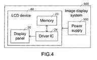
- FIG. 4is a schematic functional block diagram illustrating an image display system of some embodiments of the present invention.
- FIG. 2is a schematic functional block diagram illustrating a contrast ratio improving device according to an embodiment of the present invention.
- the contrast ratio improving deviceis applied to a display panel 20 .
- the contrast ratio improving deviceincludes a controller 21 , a photo detector 22 and a memory 23 .
- the controller 21is electrically connected to the display panel 20 through a driver IC 24 .
- the controller 21provides multiple voltage values to the driver IC 24 , so that the display panel 20 is driven by the driver IC 24 . According to these voltage values, the display panel 20 will exhibit different brightness values.
- the display panel 20will exhibit a black screen of different brightness values.
- the photo detector 22will convert the brightness values into corresponding electronic signals and transmit the electronic signals to the controller 21 .
- the controller 21will select a voltage value corresponding to a specified value (e.g. a minimum value) of the brightness values as a black voltage of the display panel 20 .
- the specified value indicative of the black voltageis then stored into the memory 23 .
- the memory 23is included in the driver IC 24 .
- the driver IC 24will read the specified value from the memory 23 so as to acquire an optimal black voltage of the display panel 20 .
- the display panel 20will exhibit an optimal contrast ratio.
- the contrast ratio improving deviceis capable of acquiring an optimal black voltage of individual display panel, the contrast ratio of individual display panel is improved.
- FIG. 3is a flowchart illustrating a contrast ratio improving method of the present invention.
- multiple voltage valuesare applied to the display panel (Step 301 ).
- the display panelwill exhibit different brightness values.
- these brightness valuesare detected (Step 302 ).
- a voltage corresponding to an extreme value of the brightness valuesis selected as a peak voltage of the display panel (Step 303 ).
- the peak voltageis stored in the memory (Step 304 ). According to the peak voltage, the contrast ratio of the display panel can be improved.
- the extreme value of the brightness valuesis the minimum value of the brightness values and the peak voltage is a black voltage.
- the driver IC 24In response to the voltage ranged from zero to the peak voltage (i.e. the black voltage), the driver IC 24 will drive the normally white LCD panel to exhibit multiple values of the brightness values.
- the extreme value of the brightness valuesis the maximum value of the brightness values and the peak voltage is a white voltage.
- the driver IC 24In response to the voltage ranged from zero to the peak voltage (i.e. the white voltage), the driver IC 24 will drive the normally black LCD panel to exhibit multiple values of the brightness values.
- FIG. 4is a schematic functional block diagram illustrating an image display system of some embodiments of the present invention.
- the image display system 600comprises a LCD device 60 and a power supply 500 .
- the LCD device 60includes a display panel 20 , a memory 23 and a driver IC 24 .
- the contrast ratio improving deviceis integrated into the display panel 20 .
- the memory 23has previously stored the peak value obtained by the contrast ratio improving method of the present invention.
- the driver IC 24drives the display panel 20 to exhibit different values of the brightness values.
- the power supply apparatus 500is electrically connected to the LCD device 60 for providing electric energy to the LCD device 60 .
- the memory 23is for example a non-volatile memory such as an erasable non-volatile memory (e.g. a flash memory) or a one-time programming (OTP) non-volatile memory.
- the memory 23can be integrated into the driver IC 24 or other IC. Alternatively, the memory 23 can be separated from the driver IC 24 .
- An example of the image display system 600includes but is not limited to a mobile phone, a digital camera, a personal digital assistant, a notebook computer, a desktop computer, a TV set, a global positioning system (GPS), an automotive display system, a flight display system, a digital photo frame, a portable DVD player, and the like.
- Some embodiments of the present inventionare illustrated by referring to a LCD device. Nevertheless, the present invention is applicable to other display device such as an organic light emitting diode (OLED) device.
- OLEDorganic light emitting diode
Landscapes
- Engineering & Computer Science (AREA)
- Chemical & Material Sciences (AREA)
- Crystallography & Structural Chemistry (AREA)
- Physics & Mathematics (AREA)
- Computer Hardware Design (AREA)
- General Physics & Mathematics (AREA)
- Theoretical Computer Science (AREA)
- Liquid Crystal Display Device Control (AREA)
- Control Of Indicators Other Than Cathode Ray Tubes (AREA)
Abstract
Description
Claims (13)
Priority Applications (1)
| Application Number | Priority Date | Filing Date | Title |
|---|---|---|---|
| US12/571,368US8791930B2 (en) | 2009-09-30 | 2009-09-30 | Device and method for improving contrast ratio of display panel and image display system |
Applications Claiming Priority (1)
| Application Number | Priority Date | Filing Date | Title |
|---|---|---|---|
| US12/571,368US8791930B2 (en) | 2009-09-30 | 2009-09-30 | Device and method for improving contrast ratio of display panel and image display system |
Publications (2)
| Publication Number | Publication Date |
|---|---|
| US20110074751A1 US20110074751A1 (en) | 2011-03-31 |
| US8791930B2true US8791930B2 (en) | 2014-07-29 |
Family
ID=43779792
Family Applications (1)
| Application Number | Title | Priority Date | Filing Date |
|---|---|---|---|
| US12/571,368Active2031-11-14US8791930B2 (en) | 2009-09-30 | 2009-09-30 | Device and method for improving contrast ratio of display panel and image display system |
Country Status (1)
| Country | Link |
|---|---|
| US (1) | US8791930B2 (en) |
Families Citing this family (5)
| Publication number | Priority date | Publication date | Assignee | Title |
|---|---|---|---|---|
| JP5105122B2 (en)* | 2008-10-16 | 2012-12-19 | Necディスプレイソリューションズ株式会社 | Image information detection device |
| US8884848B2 (en)* | 2009-05-12 | 2014-11-11 | Koninklijke Philips N.V. | Driver for an OLED device |
| KR20170072423A (en)* | 2015-12-16 | 2017-06-27 | 삼성디스플레이 주식회사 | Display apparatus and method of driving the same |
| CN111739452B (en)* | 2020-06-16 | 2022-06-07 | 深圳市华星光电半导体显示技术有限公司 | Method and device for debugging dark state voltage of liquid crystal display panel and storage medium |
| CN117577060A (en)* | 2023-11-20 | 2024-02-20 | 信利半导体有限公司 | TFT module contrast adjustment method, system, electronic equipment and storage medium |
Citations (11)
| Publication number | Priority date | Publication date | Assignee | Title |
|---|---|---|---|---|
| JPH04194818A (en) | 1990-11-22 | 1992-07-14 | Casio Comput Co Ltd | Liquid crystal display control device |
| US20030058211A1 (en) | 2001-09-03 | 2003-03-27 | Sang-Il Kim | Liquid crystal display for wide viewing angle, and driving method thereof |
| US20060290618A1 (en)* | 2003-09-05 | 2006-12-28 | Masaharu Goto | Display panel conversion data deciding method and measuring apparatus |
| US20070152949A1 (en)* | 2003-11-19 | 2007-07-05 | Yoshikazu Sakai | Luminance control method, liquid crystal display device and computer program |
| US20070290958A1 (en)* | 2006-06-16 | 2007-12-20 | Eastman Kodak Company | Method and apparatus for averaged luminance and uniformity correction in an amoled display |
| TW200827824A (en) | 2006-12-26 | 2008-07-01 | Tpo Displays Corp | Liquid crystal display devices and systems for displaying images |
| JP4194818B2 (en) | 2002-09-26 | 2008-12-10 | デルタ工業株式会社 | Seat reclining device |
| US20100007593A1 (en)* | 2008-07-09 | 2010-01-14 | Nec Lcd Technologies, Ltd. | Liquid crystal display unit driven in a longitudinal-electric-field mode |
| US20100026731A1 (en)* | 2008-07-31 | 2010-02-04 | Sony Corporation | Image processing circuit and image display apparatus |
| US20100123651A1 (en)* | 2008-11-14 | 2010-05-20 | Miller Michael E | Method for dimming electroluminescent display |
| US20120038865A1 (en) | 2006-11-03 | 2012-02-16 | Au Optronics Corporation | Liquid crystal display panel and active device array substrate thereof |
Family Cites Families (1)
| Publication number | Priority date | Publication date | Assignee | Title |
|---|---|---|---|---|
| JP2008268384A (en)* | 2007-04-17 | 2008-11-06 | Nec Lcd Technologies Ltd | Liquid crystal display |
- 2009
- 2009-09-30USUS12/571,368patent/US8791930B2/enactiveActive
Patent Citations (11)
| Publication number | Priority date | Publication date | Assignee | Title |
|---|---|---|---|---|
| JPH04194818A (en) | 1990-11-22 | 1992-07-14 | Casio Comput Co Ltd | Liquid crystal display control device |
| US20030058211A1 (en) | 2001-09-03 | 2003-03-27 | Sang-Il Kim | Liquid crystal display for wide viewing angle, and driving method thereof |
| JP4194818B2 (en) | 2002-09-26 | 2008-12-10 | デルタ工業株式会社 | Seat reclining device |
| US20060290618A1 (en)* | 2003-09-05 | 2006-12-28 | Masaharu Goto | Display panel conversion data deciding method and measuring apparatus |
| US20070152949A1 (en)* | 2003-11-19 | 2007-07-05 | Yoshikazu Sakai | Luminance control method, liquid crystal display device and computer program |
| US20070290958A1 (en)* | 2006-06-16 | 2007-12-20 | Eastman Kodak Company | Method and apparatus for averaged luminance and uniformity correction in an amoled display |
| US20120038865A1 (en) | 2006-11-03 | 2012-02-16 | Au Optronics Corporation | Liquid crystal display panel and active device array substrate thereof |
| TW200827824A (en) | 2006-12-26 | 2008-07-01 | Tpo Displays Corp | Liquid crystal display devices and systems for displaying images |
| US20100007593A1 (en)* | 2008-07-09 | 2010-01-14 | Nec Lcd Technologies, Ltd. | Liquid crystal display unit driven in a longitudinal-electric-field mode |
| US20100026731A1 (en)* | 2008-07-31 | 2010-02-04 | Sony Corporation | Image processing circuit and image display apparatus |
| US20100123651A1 (en)* | 2008-11-14 | 2010-05-20 | Miller Michael E | Method for dimming electroluminescent display |
Also Published As
| Publication number | Publication date |
|---|---|
| US20110074751A1 (en) | 2011-03-31 |
Similar Documents
| Publication | Publication Date | Title |
|---|---|---|
| US9378707B2 (en) | Gamma voltage generation unit and display device using the same | |
| US8054286B2 (en) | Liquid crystal display capable of adjusting brightness of backlight thereof and method for driving same | |
| EP3789996A1 (en) | Optical compensation method and device, display device, display method and storage medium | |
| US10504461B2 (en) | Display apparatus and display method | |
| US8552969B2 (en) | Backlight adjusting system and method | |
| US20180166030A1 (en) | Driving apparatus and method | |
| US8791930B2 (en) | Device and method for improving contrast ratio of display panel and image display system | |
| US7253813B2 (en) | Electro-optical device, driving method thereof, and electronic apparatus | |
| EP1887550A2 (en) | System and method for reducing mura defects | |
| JP5362452B2 (en) | Display device and driving method thereof | |
| US20070153117A1 (en) | Apparatus and method for adjusting display-related setting of an electronic device | |
| US9620052B2 (en) | Method of controlling a dimming operation, dimming operation control device, and flat panel display device having the same | |
| US20090237338A1 (en) | Liquid crystal display device and driving method thereof, over-drive correction device and data production method thereof and electronic device | |
| CN114582284A (en) | Display driving method, display driver and display device | |
| US20090027577A1 (en) | Liquid crystal display element, electronic paper having the same, and image processing method | |
| US20060209006A1 (en) | LCD display module | |
| US20110074836A1 (en) | Display driver capable of selectively providing gamma correction and display apparatus using same | |
| US20100134477A1 (en) | Liquid crystal display device and method of driving the same | |
| US20100013850A1 (en) | Liquid crystal display device | |
| JP2007226045A (en) | Organic el display device and coordinate input method | |
| CN100442331C (en) | Flat panel display and image correction circuit and method thereof | |
| JP2008064828A (en) | Liquid crystal device and electronic apparatus | |
| JP2009116036A (en) | Liquid crystal display, liquid crystal display program and liquid crystal display method | |
| JPWO2008038357A1 (en) | Display element, display system including the same, and image processing method | |
| KR20180079563A (en) | Optical Compensation Method of Display Device |
Legal Events
| Date | Code | Title | Description |
|---|---|---|---|
| AS | Assignment | Owner name:TPO DISPLAYS CORP., TAIWAN Free format text:ASSIGNMENT OF ASSIGNORS INTEREST;ASSIGNORS:JIANG, JIAN-XUN;WANG, SQUARE;SIGNING DATES FROM 20090803 TO 20090923;REEL/FRAME:023414/0164 | |
| AS | Assignment | Owner name:CHIMEI INNOLUX CORPORATION, TAIWAN Free format text:MERGER;ASSIGNOR:TPO DISPLAYS CORP.;REEL/FRAME:025801/0635 Effective date:20100318 | |
| AS | Assignment | Owner name:INNOLUX CORPORATION, TAIWAN Free format text:CHANGE OF NAME;ASSIGNOR:CHIMEI INNOLUX CORPORATION;REEL/FRAME:030401/0178 Effective date:20121219 | |
| STCF | Information on status: patent grant | Free format text:PATENTED CASE | |
| MAFP | Maintenance fee payment | Free format text:PAYMENT OF MAINTENANCE FEE, 4TH YEAR, LARGE ENTITY (ORIGINAL EVENT CODE: M1551) Year of fee payment:4 | |
| MAFP | Maintenance fee payment | Free format text:PAYMENT OF MAINTENANCE FEE, 8TH YEAR, LARGE ENTITY (ORIGINAL EVENT CODE: M1552); ENTITY STATUS OF PATENT OWNER: LARGE ENTITY Year of fee payment:8 |