US8791549B2 - Wafer backside interconnect structure connected to TSVs - Google Patents
Wafer backside interconnect structure connected to TSVsDownload PDFInfo
- Publication number
- US8791549B2 US8791549B2US12/832,019US83201910AUS8791549B2US 8791549 B2US8791549 B2US 8791549B2US 83201910 AUS83201910 AUS 83201910AUS 8791549 B2US8791549 B2US 8791549B2
- Authority
- US
- United States
- Prior art keywords
- integrated circuit
- semiconductor substrate
- circuit structure
- metal
- tsv
- Prior art date
- Legal status (The legal status is an assumption and is not a legal conclusion. Google has not performed a legal analysis and makes no representation as to the accuracy of the status listed.)
- Active, expires
Links
Images


Classifications
- H—ELECTRICITY
- H01—ELECTRIC ELEMENTS
- H01L—SEMICONDUCTOR DEVICES NOT COVERED BY CLASS H10
- H01L24/00—Arrangements for connecting or disconnecting semiconductor or solid-state bodies; Methods or apparatus related thereto
- H01L24/80—Methods for connecting semiconductor or other solid state bodies using means for bonding being attached to, or being formed on, the surface to be connected
- H01L24/81—Methods for connecting semiconductor or other solid state bodies using means for bonding being attached to, or being formed on, the surface to be connected using a bump connector
- H—ELECTRICITY
- H01—ELECTRIC ELEMENTS
- H01L—SEMICONDUCTOR DEVICES NOT COVERED BY CLASS H10
- H01L23/00—Details of semiconductor or other solid state devices
- H01L23/48—Arrangements for conducting electric current to or from the solid state body in operation, e.g. leads, terminal arrangements ; Selection of materials therefor
- H01L23/481—Internal lead connections, e.g. via connections, feedthrough structures
- H—ELECTRICITY
- H01—ELECTRIC ELEMENTS
- H01L—SEMICONDUCTOR DEVICES NOT COVERED BY CLASS H10
- H01L21/00—Processes or apparatus adapted for the manufacture or treatment of semiconductor or solid state devices or of parts thereof
- H01L21/70—Manufacture or treatment of devices consisting of a plurality of solid state components formed in or on a common substrate or of parts thereof; Manufacture of integrated circuit devices or of parts thereof
- H01L21/71—Manufacture of specific parts of devices defined in group H01L21/70
- H01L21/768—Applying interconnections to be used for carrying current between separate components within a device comprising conductors and dielectrics
- H01L21/76801—Applying interconnections to be used for carrying current between separate components within a device comprising conductors and dielectrics characterised by the formation and the after-treatment of the dielectrics, e.g. smoothing
- H01L21/76802—Applying interconnections to be used for carrying current between separate components within a device comprising conductors and dielectrics characterised by the formation and the after-treatment of the dielectrics, e.g. smoothing by forming openings in dielectrics
- H01L21/76807—Applying interconnections to be used for carrying current between separate components within a device comprising conductors and dielectrics characterised by the formation and the after-treatment of the dielectrics, e.g. smoothing by forming openings in dielectrics for dual damascene structures
- H01L21/76813—Applying interconnections to be used for carrying current between separate components within a device comprising conductors and dielectrics characterised by the formation and the after-treatment of the dielectrics, e.g. smoothing by forming openings in dielectrics for dual damascene structures involving a partial via etch
- H—ELECTRICITY
- H01—ELECTRIC ELEMENTS
- H01L—SEMICONDUCTOR DEVICES NOT COVERED BY CLASS H10
- H01L21/00—Processes or apparatus adapted for the manufacture or treatment of semiconductor or solid state devices or of parts thereof
- H01L21/70—Manufacture or treatment of devices consisting of a plurality of solid state components formed in or on a common substrate or of parts thereof; Manufacture of integrated circuit devices or of parts thereof
- H01L21/71—Manufacture of specific parts of devices defined in group H01L21/70
- H01L21/768—Applying interconnections to be used for carrying current between separate components within a device comprising conductors and dielectrics
- H01L21/76801—Applying interconnections to be used for carrying current between separate components within a device comprising conductors and dielectrics characterised by the formation and the after-treatment of the dielectrics, e.g. smoothing
- H01L21/76802—Applying interconnections to be used for carrying current between separate components within a device comprising conductors and dielectrics characterised by the formation and the after-treatment of the dielectrics, e.g. smoothing by forming openings in dielectrics
- H01L21/76816—Aspects relating to the layout of the pattern or to the size of vias or trenches
- H—ELECTRICITY
- H01—ELECTRIC ELEMENTS
- H01L—SEMICONDUCTOR DEVICES NOT COVERED BY CLASS H10
- H01L21/00—Processes or apparatus adapted for the manufacture or treatment of semiconductor or solid state devices or of parts thereof
- H01L21/70—Manufacture or treatment of devices consisting of a plurality of solid state components formed in or on a common substrate or of parts thereof; Manufacture of integrated circuit devices or of parts thereof
- H01L21/71—Manufacture of specific parts of devices defined in group H01L21/70
- H01L21/768—Applying interconnections to be used for carrying current between separate components within a device comprising conductors and dielectrics
- H01L21/76838—Applying interconnections to be used for carrying current between separate components within a device comprising conductors and dielectrics characterised by the formation and the after-treatment of the conductors
- H01L21/76841—Barrier, adhesion or liner layers
- H01L21/76843—Barrier, adhesion or liner layers formed in openings in a dielectric
- H—ELECTRICITY
- H01—ELECTRIC ELEMENTS
- H01L—SEMICONDUCTOR DEVICES NOT COVERED BY CLASS H10
- H01L21/00—Processes or apparatus adapted for the manufacture or treatment of semiconductor or solid state devices or of parts thereof
- H01L21/70—Manufacture or treatment of devices consisting of a plurality of solid state components formed in or on a common substrate or of parts thereof; Manufacture of integrated circuit devices or of parts thereof
- H01L21/71—Manufacture of specific parts of devices defined in group H01L21/70
- H01L21/768—Applying interconnections to be used for carrying current between separate components within a device comprising conductors and dielectrics
- H01L21/76838—Applying interconnections to be used for carrying current between separate components within a device comprising conductors and dielectrics characterised by the formation and the after-treatment of the conductors
- H01L21/76877—Filling of holes, grooves or trenches, e.g. vias, with conductive material
- H—ELECTRICITY
- H01—ELECTRIC ELEMENTS
- H01L—SEMICONDUCTOR DEVICES NOT COVERED BY CLASS H10
- H01L21/00—Processes or apparatus adapted for the manufacture or treatment of semiconductor or solid state devices or of parts thereof
- H01L21/70—Manufacture or treatment of devices consisting of a plurality of solid state components formed in or on a common substrate or of parts thereof; Manufacture of integrated circuit devices or of parts thereof
- H01L21/71—Manufacture of specific parts of devices defined in group H01L21/70
- H01L21/768—Applying interconnections to be used for carrying current between separate components within a device comprising conductors and dielectrics
- H01L21/76898—Applying interconnections to be used for carrying current between separate components within a device comprising conductors and dielectrics formed through a semiconductor substrate
- H—ELECTRICITY
- H01—ELECTRIC ELEMENTS
- H01L—SEMICONDUCTOR DEVICES NOT COVERED BY CLASS H10
- H01L24/00—Arrangements for connecting or disconnecting semiconductor or solid-state bodies; Methods or apparatus related thereto
- H01L24/01—Means for bonding being attached to, or being formed on, the surface to be connected, e.g. chip-to-package, die-attach, "first-level" interconnects; Manufacturing methods related thereto
- H01L24/02—Bonding areas ; Manufacturing methods related thereto
- H01L24/03—Manufacturing methods
- H—ELECTRICITY
- H01—ELECTRIC ELEMENTS
- H01L—SEMICONDUCTOR DEVICES NOT COVERED BY CLASS H10
- H01L24/00—Arrangements for connecting or disconnecting semiconductor or solid-state bodies; Methods or apparatus related thereto
- H01L24/01—Means for bonding being attached to, or being formed on, the surface to be connected, e.g. chip-to-package, die-attach, "first-level" interconnects; Manufacturing methods related thereto
- H01L24/02—Bonding areas ; Manufacturing methods related thereto
- H01L24/04—Structure, shape, material or disposition of the bonding areas prior to the connecting process
- H01L24/05—Structure, shape, material or disposition of the bonding areas prior to the connecting process of an individual bonding area
- H—ELECTRICITY
- H01—ELECTRIC ELEMENTS
- H01L—SEMICONDUCTOR DEVICES NOT COVERED BY CLASS H10
- H01L24/00—Arrangements for connecting or disconnecting semiconductor or solid-state bodies; Methods or apparatus related thereto
- H01L24/01—Means for bonding being attached to, or being formed on, the surface to be connected, e.g. chip-to-package, die-attach, "first-level" interconnects; Manufacturing methods related thereto
- H01L24/10—Bump connectors ; Manufacturing methods related thereto
- H01L24/11—Manufacturing methods
- H—ELECTRICITY
- H01—ELECTRIC ELEMENTS
- H01L—SEMICONDUCTOR DEVICES NOT COVERED BY CLASS H10
- H01L24/00—Arrangements for connecting or disconnecting semiconductor or solid-state bodies; Methods or apparatus related thereto
- H01L24/01—Means for bonding being attached to, or being formed on, the surface to be connected, e.g. chip-to-package, die-attach, "first-level" interconnects; Manufacturing methods related thereto
- H01L24/10—Bump connectors ; Manufacturing methods related thereto
- H01L24/12—Structure, shape, material or disposition of the bump connectors prior to the connecting process
- H01L24/13—Structure, shape, material or disposition of the bump connectors prior to the connecting process of an individual bump connector
- H—ELECTRICITY
- H01—ELECTRIC ELEMENTS
- H01L—SEMICONDUCTOR DEVICES NOT COVERED BY CLASS H10
- H01L24/00—Arrangements for connecting or disconnecting semiconductor or solid-state bodies; Methods or apparatus related thereto
- H01L24/01—Means for bonding being attached to, or being formed on, the surface to be connected, e.g. chip-to-package, die-attach, "first-level" interconnects; Manufacturing methods related thereto
- H01L24/10—Bump connectors ; Manufacturing methods related thereto
- H01L24/12—Structure, shape, material or disposition of the bump connectors prior to the connecting process
- H01L24/14—Structure, shape, material or disposition of the bump connectors prior to the connecting process of a plurality of bump connectors
- H—ELECTRICITY
- H01—ELECTRIC ELEMENTS
- H01L—SEMICONDUCTOR DEVICES NOT COVERED BY CLASS H10
- H01L2224/00—Indexing scheme for arrangements for connecting or disconnecting semiconductor or solid-state bodies and methods related thereto as covered by H01L24/00
- H01L2224/01—Means for bonding being attached to, or being formed on, the surface to be connected, e.g. chip-to-package, die-attach, "first-level" interconnects; Manufacturing methods related thereto
- H01L2224/02—Bonding areas; Manufacturing methods related thereto
- H01L2224/04—Structure, shape, material or disposition of the bonding areas prior to the connecting process
- H01L2224/0401—Bonding areas specifically adapted for bump connectors, e.g. under bump metallisation [UBM]
- H—ELECTRICITY
- H01—ELECTRIC ELEMENTS
- H01L—SEMICONDUCTOR DEVICES NOT COVERED BY CLASS H10
- H01L2224/00—Indexing scheme for arrangements for connecting or disconnecting semiconductor or solid-state bodies and methods related thereto as covered by H01L24/00
- H01L2224/01—Means for bonding being attached to, or being formed on, the surface to be connected, e.g. chip-to-package, die-attach, "first-level" interconnects; Manufacturing methods related thereto
- H01L2224/02—Bonding areas; Manufacturing methods related thereto
- H01L2224/04—Structure, shape, material or disposition of the bonding areas prior to the connecting process
- H01L2224/05—Structure, shape, material or disposition of the bonding areas prior to the connecting process of an individual bonding area
- H01L2224/05001—Internal layers
- H01L2224/0502—Disposition
- H01L2224/05022—Disposition the internal layer being at least partially embedded in the surface
- H—ELECTRICITY
- H01—ELECTRIC ELEMENTS
- H01L—SEMICONDUCTOR DEVICES NOT COVERED BY CLASS H10
- H01L2224/00—Indexing scheme for arrangements for connecting or disconnecting semiconductor or solid-state bodies and methods related thereto as covered by H01L24/00
- H01L2224/01—Means for bonding being attached to, or being formed on, the surface to be connected, e.g. chip-to-package, die-attach, "first-level" interconnects; Manufacturing methods related thereto
- H01L2224/02—Bonding areas; Manufacturing methods related thereto
- H01L2224/04—Structure, shape, material or disposition of the bonding areas prior to the connecting process
- H01L2224/05—Structure, shape, material or disposition of the bonding areas prior to the connecting process of an individual bonding area
- H01L2224/05001—Internal layers
- H01L2224/0502—Disposition
- H01L2224/05025—Disposition the internal layer being disposed on a via connection of the semiconductor or solid-state body
- H—ELECTRICITY
- H01—ELECTRIC ELEMENTS
- H01L—SEMICONDUCTOR DEVICES NOT COVERED BY CLASS H10
- H01L2224/00—Indexing scheme for arrangements for connecting or disconnecting semiconductor or solid-state bodies and methods related thereto as covered by H01L24/00
- H01L2224/01—Means for bonding being attached to, or being formed on, the surface to be connected, e.g. chip-to-package, die-attach, "first-level" interconnects; Manufacturing methods related thereto
- H01L2224/02—Bonding areas; Manufacturing methods related thereto
- H01L2224/04—Structure, shape, material or disposition of the bonding areas prior to the connecting process
- H01L2224/05—Structure, shape, material or disposition of the bonding areas prior to the connecting process of an individual bonding area
- H01L2224/0554—External layer
- H01L2224/05541—Structure
- H01L2224/05546—Dual damascene structure
- H—ELECTRICITY
- H01—ELECTRIC ELEMENTS
- H01L—SEMICONDUCTOR DEVICES NOT COVERED BY CLASS H10
- H01L2224/00—Indexing scheme for arrangements for connecting or disconnecting semiconductor or solid-state bodies and methods related thereto as covered by H01L24/00
- H01L2224/01—Means for bonding being attached to, or being formed on, the surface to be connected, e.g. chip-to-package, die-attach, "first-level" interconnects; Manufacturing methods related thereto
- H01L2224/02—Bonding areas; Manufacturing methods related thereto
- H01L2224/04—Structure, shape, material or disposition of the bonding areas prior to the connecting process
- H01L2224/05—Structure, shape, material or disposition of the bonding areas prior to the connecting process of an individual bonding area
- H01L2224/0554—External layer
- H01L2224/05541—Structure
- H01L2224/05547—Structure comprising a core and a coating
- H—ELECTRICITY
- H01—ELECTRIC ELEMENTS
- H01L—SEMICONDUCTOR DEVICES NOT COVERED BY CLASS H10
- H01L2224/00—Indexing scheme for arrangements for connecting or disconnecting semiconductor or solid-state bodies and methods related thereto as covered by H01L24/00
- H01L2224/01—Means for bonding being attached to, or being formed on, the surface to be connected, e.g. chip-to-package, die-attach, "first-level" interconnects; Manufacturing methods related thereto
- H01L2224/02—Bonding areas; Manufacturing methods related thereto
- H01L2224/04—Structure, shape, material or disposition of the bonding areas prior to the connecting process
- H01L2224/05—Structure, shape, material or disposition of the bonding areas prior to the connecting process of an individual bonding area
- H01L2224/0554—External layer
- H01L2224/0556—Disposition
- H01L2224/05567—Disposition the external layer being at least partially embedded in the surface
- H—ELECTRICITY
- H01—ELECTRIC ELEMENTS
- H01L—SEMICONDUCTOR DEVICES NOT COVERED BY CLASS H10
- H01L2224/00—Indexing scheme for arrangements for connecting or disconnecting semiconductor or solid-state bodies and methods related thereto as covered by H01L24/00
- H01L2224/01—Means for bonding being attached to, or being formed on, the surface to be connected, e.g. chip-to-package, die-attach, "first-level" interconnects; Manufacturing methods related thereto
- H01L2224/02—Bonding areas; Manufacturing methods related thereto
- H01L2224/04—Structure, shape, material or disposition of the bonding areas prior to the connecting process
- H01L2224/05—Structure, shape, material or disposition of the bonding areas prior to the connecting process of an individual bonding area
- H01L2224/0554—External layer
- H01L2224/0556—Disposition
- H01L2224/0557—Disposition the external layer being disposed on a via connection of the semiconductor or solid-state body
- H—ELECTRICITY
- H01—ELECTRIC ELEMENTS
- H01L—SEMICONDUCTOR DEVICES NOT COVERED BY CLASS H10
- H01L2224/00—Indexing scheme for arrangements for connecting or disconnecting semiconductor or solid-state bodies and methods related thereto as covered by H01L24/00
- H01L2224/01—Means for bonding being attached to, or being formed on, the surface to be connected, e.g. chip-to-package, die-attach, "first-level" interconnects; Manufacturing methods related thereto
- H01L2224/02—Bonding areas; Manufacturing methods related thereto
- H01L2224/04—Structure, shape, material or disposition of the bonding areas prior to the connecting process
- H01L2224/05—Structure, shape, material or disposition of the bonding areas prior to the connecting process of an individual bonding area
- H01L2224/0554—External layer
- H01L2224/0556—Disposition
- H01L2224/05571—Disposition the external layer being disposed in a recess of the surface
- H—ELECTRICITY
- H01—ELECTRIC ELEMENTS
- H01L—SEMICONDUCTOR DEVICES NOT COVERED BY CLASS H10
- H01L2224/00—Indexing scheme for arrangements for connecting or disconnecting semiconductor or solid-state bodies and methods related thereto as covered by H01L24/00
- H01L2224/01—Means for bonding being attached to, or being formed on, the surface to be connected, e.g. chip-to-package, die-attach, "first-level" interconnects; Manufacturing methods related thereto
- H01L2224/02—Bonding areas; Manufacturing methods related thereto
- H01L2224/04—Structure, shape, material or disposition of the bonding areas prior to the connecting process
- H01L2224/06—Structure, shape, material or disposition of the bonding areas prior to the connecting process of a plurality of bonding areas
- H01L2224/061—Disposition
- H01L2224/0618—Disposition being disposed on at least two different sides of the body, e.g. dual array
- H01L2224/06181—On opposite sides of the body
- H—ELECTRICITY
- H01—ELECTRIC ELEMENTS
- H01L—SEMICONDUCTOR DEVICES NOT COVERED BY CLASS H10
- H01L2224/00—Indexing scheme for arrangements for connecting or disconnecting semiconductor or solid-state bodies and methods related thereto as covered by H01L24/00
- H01L2224/01—Means for bonding being attached to, or being formed on, the surface to be connected, e.g. chip-to-package, die-attach, "first-level" interconnects; Manufacturing methods related thereto
- H01L2224/10—Bump connectors; Manufacturing methods related thereto
- H01L2224/12—Structure, shape, material or disposition of the bump connectors prior to the connecting process
- H01L2224/13—Structure, shape, material or disposition of the bump connectors prior to the connecting process of an individual bump connector
- H01L2224/13001—Core members of the bump connector
- H01L2224/13005—Structure
- H01L2224/13007—Bump connector smaller than the underlying bonding area, e.g. than the under bump metallisation [UBM]
- H—ELECTRICITY
- H01—ELECTRIC ELEMENTS
- H01L—SEMICONDUCTOR DEVICES NOT COVERED BY CLASS H10
- H01L2224/00—Indexing scheme for arrangements for connecting or disconnecting semiconductor or solid-state bodies and methods related thereto as covered by H01L24/00
- H01L2224/01—Means for bonding being attached to, or being formed on, the surface to be connected, e.g. chip-to-package, die-attach, "first-level" interconnects; Manufacturing methods related thereto
- H01L2224/10—Bump connectors; Manufacturing methods related thereto
- H01L2224/12—Structure, shape, material or disposition of the bump connectors prior to the connecting process
- H01L2224/13—Structure, shape, material or disposition of the bump connectors prior to the connecting process of an individual bump connector
- H01L2224/13001—Core members of the bump connector
- H01L2224/1302—Disposition
- H01L2224/13022—Disposition the bump connector being at least partially embedded in the surface
- H—ELECTRICITY
- H01—ELECTRIC ELEMENTS
- H01L—SEMICONDUCTOR DEVICES NOT COVERED BY CLASS H10
- H01L2224/00—Indexing scheme for arrangements for connecting or disconnecting semiconductor or solid-state bodies and methods related thereto as covered by H01L24/00
- H01L2224/01—Means for bonding being attached to, or being formed on, the surface to be connected, e.g. chip-to-package, die-attach, "first-level" interconnects; Manufacturing methods related thereto
- H01L2224/10—Bump connectors; Manufacturing methods related thereto
- H01L2224/12—Structure, shape, material or disposition of the bump connectors prior to the connecting process
- H01L2224/13—Structure, shape, material or disposition of the bump connectors prior to the connecting process of an individual bump connector
- H01L2224/13001—Core members of the bump connector
- H01L2224/1302—Disposition
- H01L2224/13025—Disposition the bump connector being disposed on a via connection of the semiconductor or solid-state body
- H—ELECTRICITY
- H01—ELECTRIC ELEMENTS
- H01L—SEMICONDUCTOR DEVICES NOT COVERED BY CLASS H10
- H01L2224/00—Indexing scheme for arrangements for connecting or disconnecting semiconductor or solid-state bodies and methods related thereto as covered by H01L24/00
- H01L2224/01—Means for bonding being attached to, or being formed on, the surface to be connected, e.g. chip-to-package, die-attach, "first-level" interconnects; Manufacturing methods related thereto
- H01L2224/10—Bump connectors; Manufacturing methods related thereto
- H01L2224/12—Structure, shape, material or disposition of the bump connectors prior to the connecting process
- H01L2224/13—Structure, shape, material or disposition of the bump connectors prior to the connecting process of an individual bump connector
- H01L2224/13001—Core members of the bump connector
- H01L2224/13099—Material
- H01L2224/131—Material with a principal constituent of the material being a metal or a metalloid, e.g. boron [B], silicon [Si], germanium [Ge], arsenic [As], antimony [Sb], tellurium [Te] and polonium [Po], and alloys thereof
- H01L2224/13138—Material with a principal constituent of the material being a metal or a metalloid, e.g. boron [B], silicon [Si], germanium [Ge], arsenic [As], antimony [Sb], tellurium [Te] and polonium [Po], and alloys thereof the principal constituent melting at a temperature of greater than or equal to 950°C and less than 1550°C
- H01L2224/13144—Gold [Au] as principal constituent
- H—ELECTRICITY
- H01—ELECTRIC ELEMENTS
- H01L—SEMICONDUCTOR DEVICES NOT COVERED BY CLASS H10
- H01L2224/00—Indexing scheme for arrangements for connecting or disconnecting semiconductor or solid-state bodies and methods related thereto as covered by H01L24/00
- H01L2224/01—Means for bonding being attached to, or being formed on, the surface to be connected, e.g. chip-to-package, die-attach, "first-level" interconnects; Manufacturing methods related thereto
- H01L2224/10—Bump connectors; Manufacturing methods related thereto
- H01L2224/12—Structure, shape, material or disposition of the bump connectors prior to the connecting process
- H01L2224/13—Structure, shape, material or disposition of the bump connectors prior to the connecting process of an individual bump connector
- H01L2224/13001—Core members of the bump connector
- H01L2224/13099—Material
- H01L2224/131—Material with a principal constituent of the material being a metal or a metalloid, e.g. boron [B], silicon [Si], germanium [Ge], arsenic [As], antimony [Sb], tellurium [Te] and polonium [Po], and alloys thereof
- H01L2224/13138—Material with a principal constituent of the material being a metal or a metalloid, e.g. boron [B], silicon [Si], germanium [Ge], arsenic [As], antimony [Sb], tellurium [Te] and polonium [Po], and alloys thereof the principal constituent melting at a temperature of greater than or equal to 950°C and less than 1550°C
- H01L2224/13155—Nickel [Ni] as principal constituent
- H—ELECTRICITY
- H01—ELECTRIC ELEMENTS
- H01L—SEMICONDUCTOR DEVICES NOT COVERED BY CLASS H10
- H01L2224/00—Indexing scheme for arrangements for connecting or disconnecting semiconductor or solid-state bodies and methods related thereto as covered by H01L24/00
- H01L2224/01—Means for bonding being attached to, or being formed on, the surface to be connected, e.g. chip-to-package, die-attach, "first-level" interconnects; Manufacturing methods related thereto
- H01L2224/10—Bump connectors; Manufacturing methods related thereto
- H01L2224/12—Structure, shape, material or disposition of the bump connectors prior to the connecting process
- H01L2224/14—Structure, shape, material or disposition of the bump connectors prior to the connecting process of a plurality of bump connectors
- H01L2224/141—Disposition
- H01L2224/1418—Disposition being disposed on at least two different sides of the body, e.g. dual array
- H01L2224/14181—On opposite sides of the body
- H—ELECTRICITY
- H01—ELECTRIC ELEMENTS
- H01L—SEMICONDUCTOR DEVICES NOT COVERED BY CLASS H10
- H01L2224/00—Indexing scheme for arrangements for connecting or disconnecting semiconductor or solid-state bodies and methods related thereto as covered by H01L24/00
- H01L2224/80—Methods for connecting semiconductor or other solid state bodies using means for bonding being attached to, or being formed on, the surface to be connected
- H01L2224/81—Methods for connecting semiconductor or other solid state bodies using means for bonding being attached to, or being formed on, the surface to be connected using a bump connector
- H01L2224/811—Methods for connecting semiconductor or other solid state bodies using means for bonding being attached to, or being formed on, the surface to be connected using a bump connector the bump connector being supplied to the parts to be connected in the bonding apparatus
- H—ELECTRICITY
- H01—ELECTRIC ELEMENTS
- H01L—SEMICONDUCTOR DEVICES NOT COVERED BY CLASS H10
- H01L2224/00—Indexing scheme for arrangements for connecting or disconnecting semiconductor or solid-state bodies and methods related thereto as covered by H01L24/00
- H01L2224/80—Methods for connecting semiconductor or other solid state bodies using means for bonding being attached to, or being formed on, the surface to be connected
- H01L2224/81—Methods for connecting semiconductor or other solid state bodies using means for bonding being attached to, or being formed on, the surface to be connected using a bump connector
- H01L2224/8136—Bonding interfaces of the semiconductor or solid state body
- H—ELECTRICITY
- H01—ELECTRIC ELEMENTS
- H01L—SEMICONDUCTOR DEVICES NOT COVERED BY CLASS H10
- H01L23/00—Details of semiconductor or other solid state devices
- H01L23/28—Encapsulations, e.g. encapsulating layers, coatings, e.g. for protection
- H01L23/31—Encapsulations, e.g. encapsulating layers, coatings, e.g. for protection characterised by the arrangement or shape
- H01L23/3107—Encapsulations, e.g. encapsulating layers, coatings, e.g. for protection characterised by the arrangement or shape the device being completely enclosed
- H01L23/3114—Encapsulations, e.g. encapsulating layers, coatings, e.g. for protection characterised by the arrangement or shape the device being completely enclosed the device being a chip scale package, e.g. CSP
- H—ELECTRICITY
- H01—ELECTRIC ELEMENTS
- H01L—SEMICONDUCTOR DEVICES NOT COVERED BY CLASS H10
- H01L24/00—Arrangements for connecting or disconnecting semiconductor or solid-state bodies; Methods or apparatus related thereto
- H01L24/01—Means for bonding being attached to, or being formed on, the surface to be connected, e.g. chip-to-package, die-attach, "first-level" interconnects; Manufacturing methods related thereto
- H01L24/10—Bump connectors ; Manufacturing methods related thereto
- H01L24/15—Structure, shape, material or disposition of the bump connectors after the connecting process
- H01L24/16—Structure, shape, material or disposition of the bump connectors after the connecting process of an individual bump connector
- H—ELECTRICITY
- H01—ELECTRIC ELEMENTS
- H01L—SEMICONDUCTOR DEVICES NOT COVERED BY CLASS H10
- H01L2924/00—Indexing scheme for arrangements or methods for connecting or disconnecting semiconductor or solid-state bodies as covered by H01L24/00
- H01L2924/0001—Technical content checked by a classifier
- H01L2924/00014—Technical content checked by a classifier the subject-matter covered by the group, the symbol of which is combined with the symbol of this group, being disclosed without further technical details
- H—ELECTRICITY
- H01—ELECTRIC ELEMENTS
- H01L—SEMICONDUCTOR DEVICES NOT COVERED BY CLASS H10
- H01L2924/00—Indexing scheme for arrangements or methods for connecting or disconnecting semiconductor or solid-state bodies as covered by H01L24/00
- H01L2924/0001—Technical content checked by a classifier
- H01L2924/0002—Not covered by any one of groups H01L24/00, H01L24/00 and H01L2224/00
- H—ELECTRICITY
- H01—ELECTRIC ELEMENTS
- H01L—SEMICONDUCTOR DEVICES NOT COVERED BY CLASS H10
- H01L2924/00—Indexing scheme for arrangements or methods for connecting or disconnecting semiconductor or solid-state bodies as covered by H01L24/00
- H01L2924/01—Chemical elements
- H01L2924/01004—Beryllium [Be]
- H—ELECTRICITY
- H01—ELECTRIC ELEMENTS
- H01L—SEMICONDUCTOR DEVICES NOT COVERED BY CLASS H10
- H01L2924/00—Indexing scheme for arrangements or methods for connecting or disconnecting semiconductor or solid-state bodies as covered by H01L24/00
- H01L2924/01—Chemical elements
- H01L2924/01005—Boron [B]
- H—ELECTRICITY
- H01—ELECTRIC ELEMENTS
- H01L—SEMICONDUCTOR DEVICES NOT COVERED BY CLASS H10
- H01L2924/00—Indexing scheme for arrangements or methods for connecting or disconnecting semiconductor or solid-state bodies as covered by H01L24/00
- H01L2924/01—Chemical elements
- H01L2924/01006—Carbon [C]
- H—ELECTRICITY
- H01—ELECTRIC ELEMENTS
- H01L—SEMICONDUCTOR DEVICES NOT COVERED BY CLASS H10
- H01L2924/00—Indexing scheme for arrangements or methods for connecting or disconnecting semiconductor or solid-state bodies as covered by H01L24/00
- H01L2924/01—Chemical elements
- H01L2924/01013—Aluminum [Al]
- H—ELECTRICITY
- H01—ELECTRIC ELEMENTS
- H01L—SEMICONDUCTOR DEVICES NOT COVERED BY CLASS H10
- H01L2924/00—Indexing scheme for arrangements or methods for connecting or disconnecting semiconductor or solid-state bodies as covered by H01L24/00
- H01L2924/01—Chemical elements
- H01L2924/01014—Silicon [Si]
- H—ELECTRICITY
- H01—ELECTRIC ELEMENTS
- H01L—SEMICONDUCTOR DEVICES NOT COVERED BY CLASS H10
- H01L2924/00—Indexing scheme for arrangements or methods for connecting or disconnecting semiconductor or solid-state bodies as covered by H01L24/00
- H01L2924/01—Chemical elements
- H01L2924/01022—Titanium [Ti]
- H—ELECTRICITY
- H01—ELECTRIC ELEMENTS
- H01L—SEMICONDUCTOR DEVICES NOT COVERED BY CLASS H10
- H01L2924/00—Indexing scheme for arrangements or methods for connecting or disconnecting semiconductor or solid-state bodies as covered by H01L24/00
- H01L2924/01—Chemical elements
- H01L2924/01023—Vanadium [V]
- H—ELECTRICITY
- H01—ELECTRIC ELEMENTS
- H01L—SEMICONDUCTOR DEVICES NOT COVERED BY CLASS H10
- H01L2924/00—Indexing scheme for arrangements or methods for connecting or disconnecting semiconductor or solid-state bodies as covered by H01L24/00
- H01L2924/01—Chemical elements
- H01L2924/01029—Copper [Cu]
- H—ELECTRICITY
- H01—ELECTRIC ELEMENTS
- H01L—SEMICONDUCTOR DEVICES NOT COVERED BY CLASS H10
- H01L2924/00—Indexing scheme for arrangements or methods for connecting or disconnecting semiconductor or solid-state bodies as covered by H01L24/00
- H01L2924/01—Chemical elements
- H01L2924/01033—Arsenic [As]
- H—ELECTRICITY
- H01—ELECTRIC ELEMENTS
- H01L—SEMICONDUCTOR DEVICES NOT COVERED BY CLASS H10
- H01L2924/00—Indexing scheme for arrangements or methods for connecting or disconnecting semiconductor or solid-state bodies as covered by H01L24/00
- H01L2924/01—Chemical elements
- H01L2924/01046—Palladium [Pd]
- H—ELECTRICITY
- H01—ELECTRIC ELEMENTS
- H01L—SEMICONDUCTOR DEVICES NOT COVERED BY CLASS H10
- H01L2924/00—Indexing scheme for arrangements or methods for connecting or disconnecting semiconductor or solid-state bodies as covered by H01L24/00
- H01L2924/01—Chemical elements
- H01L2924/01073—Tantalum [Ta]
- H—ELECTRICITY
- H01—ELECTRIC ELEMENTS
- H01L—SEMICONDUCTOR DEVICES NOT COVERED BY CLASS H10
- H01L2924/00—Indexing scheme for arrangements or methods for connecting or disconnecting semiconductor or solid-state bodies as covered by H01L24/00
- H01L2924/01—Chemical elements
- H01L2924/01074—Tungsten [W]
- H—ELECTRICITY
- H01—ELECTRIC ELEMENTS
- H01L—SEMICONDUCTOR DEVICES NOT COVERED BY CLASS H10
- H01L2924/00—Indexing scheme for arrangements or methods for connecting or disconnecting semiconductor or solid-state bodies as covered by H01L24/00
- H01L2924/01—Chemical elements
- H01L2924/01078—Platinum [Pt]
- H—ELECTRICITY
- H01—ELECTRIC ELEMENTS
- H01L—SEMICONDUCTOR DEVICES NOT COVERED BY CLASS H10
- H01L2924/00—Indexing scheme for arrangements or methods for connecting or disconnecting semiconductor or solid-state bodies as covered by H01L24/00
- H01L2924/01—Chemical elements
- H01L2924/01079—Gold [Au]
- H—ELECTRICITY
- H01—ELECTRIC ELEMENTS
- H01L—SEMICONDUCTOR DEVICES NOT COVERED BY CLASS H10
- H01L2924/00—Indexing scheme for arrangements or methods for connecting or disconnecting semiconductor or solid-state bodies as covered by H01L24/00
- H01L2924/01—Chemical elements
- H01L2924/01082—Lead [Pb]
- H—ELECTRICITY
- H01—ELECTRIC ELEMENTS
- H01L—SEMICONDUCTOR DEVICES NOT COVERED BY CLASS H10
- H01L2924/00—Indexing scheme for arrangements or methods for connecting or disconnecting semiconductor or solid-state bodies as covered by H01L24/00
- H01L2924/013—Alloys
- H01L2924/0132—Binary Alloys
- H01L2924/01327—Intermediate phases, i.e. intermetallics compounds
- H—ELECTRICITY
- H01—ELECTRIC ELEMENTS
- H01L—SEMICONDUCTOR DEVICES NOT COVERED BY CLASS H10
- H01L2924/00—Indexing scheme for arrangements or methods for connecting or disconnecting semiconductor or solid-state bodies as covered by H01L24/00
- H01L2924/013—Alloys
- H01L2924/014—Solder alloys
- H—ELECTRICITY
- H01—ELECTRIC ELEMENTS
- H01L—SEMICONDUCTOR DEVICES NOT COVERED BY CLASS H10
- H01L2924/00—Indexing scheme for arrangements or methods for connecting or disconnecting semiconductor or solid-state bodies as covered by H01L24/00
- H01L2924/049—Nitrides composed of metals from groups of the periodic table
- H01L2924/0494—4th Group
- H01L2924/04941—TiN
- H—ELECTRICITY
- H01—ELECTRIC ELEMENTS
- H01L—SEMICONDUCTOR DEVICES NOT COVERED BY CLASS H10
- H01L2924/00—Indexing scheme for arrangements or methods for connecting or disconnecting semiconductor or solid-state bodies as covered by H01L24/00
- H01L2924/10—Details of semiconductor or other solid state devices to be connected
- H01L2924/11—Device type
- H01L2924/14—Integrated circuits
- H—ELECTRICITY
- H01—ELECTRIC ELEMENTS
- H01L—SEMICONDUCTOR DEVICES NOT COVERED BY CLASS H10
- H01L2924/00—Indexing scheme for arrangements or methods for connecting or disconnecting semiconductor or solid-state bodies as covered by H01L24/00
- H01L2924/19—Details of hybrid assemblies other than the semiconductor or other solid state devices to be connected
- H01L2924/1901—Structure
- H01L2924/1904—Component type
- H01L2924/19041—Component type being a capacitor
Definitions
- This disclosurerelates generally to integrated circuit structures, and more particularly to interconnect structures formed on the backside of wafers and connected to through-substrate vias.
- TSVsThrough-substrate vias
- TSVsare thus used in 3D ICs and stacked dies for connecting dies.
- TSVsare often used to connect the integrated circuits on a die to the backside of the die.
- TSVsare also used to provide short grounding paths for grounding the integrated circuits through the backside of the die, which may be covered by a grounded metallic film.
- an integrated circuit structureincludes a semiconductor substrate having a front surface and a back surface; a conductive via passing through the semiconductor substrate; and a metal feature on the back surface of the semiconductor substrate.
- the metal featureincludes a metal pad overlying and contacting the conductive via, and a metal line over the conductive via.
- the metal lineincludes a dual damascene structure.
- the integrated circuit structurefurther includes a bump overlying the metal line.
- FIGS. 1 through 12Billustrate cross-sectional views of intermediate stages in the manufacturing of a backside interconnect structure in accordance with an embodiment, in which the back surface of a substrate and a through-substrate via (TSV) are recessed;
- TSVthrough-substrate via
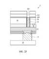
- FIGS. 13 through 23Billustrate cross-sectional views of intermediate stages in the manufacturing of a backside interconnect structure in accordance with another embodiment, in which the back surface of a substrate is recessed;
- FIGS. 24 through 29Billustrate cross-sectional views of intermediate stages in the manufacturing of a backside interconnect structure in accordance with yet another embodiment, in which the backside interconnect are formed on the back surface of a substrate.
- TSVsthrough-substrate vias
- chip 2which includes substrate 10 and integrated circuits (not shown) therein, is provided.
- Chip 2may be a portion of a wafer.
- Substrate 10may be a semiconductor substrate, such as a bulk silicon substrate, although it may include other semiconductor materials such as group III, group IV, and/or group V elements.
- Active semiconductor devicessuch as transistors (symbolized by block 15 ) may be formed on front side 10 f of substrate 10 .
- the term “backside”refers to the side of substrate 10 opposite the side having the active semiconductor devices.
- Interconnect structure 12which includes metal lines and vias (not shown) formed therein, is formed on front side 10 f of substrate 10 and connected to the active semiconductor devices.
- Interconnect structure 12may include commonly known inter-layer dielectric (ILD) and inter-metal dielectrics (IMDs).
- Bond pad 14is formed on the front side 10 f of substrate 10 .
- TSV 20is formed in substrate 10 , and extends from the front side 10 f into substrate 10 .
- TSV 20is formed using a via-first approach, and is formed before the formation of interconnect structure 12 . Accordingly, TSV 20 only extends to the ILD that is used to cover the active devices, but not into the IMD layers in interconnect structure 12 .
- TSV 20is formed using a via-last approach, and is formed after the formation of interconnect structure 12 . Accordingly, TSV 20 penetrates through both substrate 10 and interconnect structure 12 .
- Isolation layer 22is formed on the sidewalls and an end of TSV 20 , and electrically insulates TSV 20 from substrate 10 .
- Isolation layer 22may be formed of commonly used dielectric materials such as silicon nitride, silicon oxide (for example, tetra-ethyl-ortho-silicate (TEOS) oxide), and the like. Chip 2 and the corresponding wafer is adhered to carrier 25 .
- TEOStetra-ethyl-ortho-silicate
- a backside grindingis performed so that TSV 20 is exposed through the back surface 10 b of substrate 10 .
- the backside grindingmay be performed using TSV 20 as a stop layer.
- TSV 20is recessed, so that it's top surface is lower than the back surface 10 b of substrate 10 .
- the recess depth D 1may be greater than about 0.5 ⁇ m, and may be 3 ⁇ m in an exemplary embodiment.
- opening 24is formed.
- FIG. 4illustrates the recessing of substrate 10 , which is performed using photo resist 26 as a mask. As a result of the recessing, the horizontal dimension of opening 24 is increased to greater than that of TSV 20 .
- FIG. 3illustrates that in opening 24 lower portion 28 of back surface 10 b is level with the exposed end of TSV 20 . Alternatively, lower portion 28 may also be higher than or lower than the exposed end of TSV 20 , as also illustrated by dotted lines. At the same time opening 24 is formed, (trench) openings 27 are also formed.
- dielectric isolation layer 30is deposited.
- the deposition methodsinclude low-temperature chemical vapor deposition (LTCVD), although other commonly used methods may also be used.
- dielectric isolation layer 30comprises silicon nitride (SiN x ), and may have a thickness of a several hundred angstroms.
- FIGS. 7 through 9illustrate the formation of redistribution lines and pads.
- conductive barrier layer 32which may comprise titanium, titanium nitride, tantalum, tantalum nitride, or the like, is formed, for example, by sputtering. Copper 34 is then plated, as shown in FIG. 8 . The thickness of copper 34 depends on depth D 1 ( FIG. 3 ). A chemical mechanical polish (CMP) is then performed to form metal features 36 (denoted as 36 - 1 and 36 - 2 ), and the resulting structure is shown in FIG. 9 .
- Metal features 36may include metal lines 36 - 1 , which may actually be connected to other TSVs (not shown).
- metal lines 36 - 1are used as redistribution lines.
- Metal feature 36 - 2may be a metal pad or a metal line.
- the metal padmay have dimensions (viewed from top) greater than that of TSV 20 , and the metal pad may extend beyond the edges of TSV 20 in all horizontal directions. Accordingly, metal pad 36 - 2 and TSV 20 have a reliable connection with a large interface area, and hence a small contact resistance. Further, the accuracy requirement for aligning metal pad 36 - 2 to TSV 20 is relaxed.
- FIGS. 10-12Aillustrate the formation of bump 42 .
- dielectric layer 38is blanket deposited.
- dielectric layer 38comprises silicon nitride (SiN x ), and may have a thickness, for example, of about 0.2 ⁇ m.
- FIG. 11with photo resist 40 , an opening is formed in dielectric layer 38 so that metal pad 36 - 2 is exposed.
- FIG. 12Aillustrates the formation of bump 42 , which is also referred to as a micro-bump (U-bump) since it may have a horizontal dimension (length or width) of less than about 30 ⁇ m.
- the formation methods of bump 42include electrical chemical plating (ECP), electroless plating, and immersion.
- the resulting bump 42may have an electroless nickel immersion gold (ENIG) structure, a nickel electroless palladium immersion gold (ENEPIG) structure, or a nickel palladium structure. It is realized that although FIG. 12A illustrates that bump 42 is directly over metal pad 36 - 2 , bump 42 may also be not directly over metal pad 36 - 2 , and may actually be connected to metal pad 36 - 2 through a redistribution line similar to metal lines 36 - 1 , which redistribution lines are formed simultaneously with the formation of metal features 36 .
- EIGelectroless nickel immersion gold
- ENEPIGnickel electroless palladium immersion gold
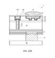
- FIG. 12Billustrates an alternative embodiment.
- additional layers of redistribution linesmay be formed.
- an additional layer 60 including etch stop layer 46 , dielectric layer 48 , via 50 , and metal line 52may be inserted between metal pad 36 - 2 and bump 42 .
- more layers similar to layer 60may be stacked on layer 60 to increase the routability of the backside interconnect structure.
- the formation details of layer 60may be essentially the same as shown in FIGS. 18-21 , as will be discussed in subsequent paragraphs.
- FIGS. 13 through 23Billustrate an alternative embodiment.
- the initial steps of this embodimentare the same as illustrated in FIGS. 1 and 2 .
- substrate 10is etched back from the backside, so that TSV 20 protrudes out of the back surface of substrate 10 .
- the etch back depth D 2is greater than about 0.5 ⁇ m, and may be about 1 ⁇ m.
- Isolation layer 22may also be etched back from the top surface of TSV 20 , for example, to about 0.5 ⁇ m lower than the top surface of TSV 20 . Accordingly, portions of sidewalls of TSV 20 are exposed.
- dielectric layer 124is formed on the back surface of substrate 10 and covers TSV 20 .
- dielectric layer 124is formed of polyimide, and may have a thickness greater than about 2 ⁇ m, with an exemplary thickness equal to about 3 ⁇ m. In alternative embodiments, other dielectric materials may be used.
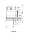
- FIGS. 15 through 17illustrate the formation of metal lines.
- openings 126are formed by etching dielectric layer 124 , for example, with the help of a photo resist (not shown).
- the opening formation processis controlled, for example, using a time mode, so that TSV 20 is exposed through one of openings 126 , while a bottom portion of dielectric layer 124 (denoted as layer 124 ′) remains to separate openings 126 from substrate 10 .
- Conductive barrier layer 128is deposited, for example, by sputtering.
- Conductive barrier layer 128may comprise titanium, tantalum, or the like.
- Metallic material 130is then plated to a level higher than the top surface of dielectric layer 124 .
- Metallic material 130may include copper, although other metals such as aluminum, tungsten, or the like, may also be used.
- a CMPis then performed, as shown in FIG. 17 , and hence metal lines/pads 132 (denoted as 132 - 1 and 132 - 2 ) are formed.
- Metal line 132 - 2may be electrically connected to one of the TSVs in the chip.
- metal line 132 - 2may be used as a redistribution line.
- Metal feature 132 - 1may be a metal pad or a metal trace.
- the metal padmay have dimensions (viewed from top) greater than that of TSV 20 , wherein in the top view, metal pad 132 - 1 may extend beyond the edges of TSV 20 in all lateral directions.
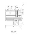
- FIGS. 18 through 21illustrate the formation of an additional layer of interconnect.
- dielectric layer 125is formed.
- dielectric layer 125is formed of polyimide, which may have a thickness of several microns such as about 2.5 ⁇ m.
- Photo resist 134is then applied and patterned. Via openings 136 are then formed by etching dielectric layer 125 through patterned photo resist 134 , until metal line 132 - 2 is exposed.
- photo resist 134is removed, and an additional photo resist 140 is formed and patterned.
- Trench openings 138are then formed by further etching dielectric layer 125 through patterned photo resist 140 , as illustrated in FIG. 20 .
- the etchingmay be performed using a time mode, so that the etching is stopped at an intermediate level of dielectric layer 125 .
- Photo resist 140is then removed, for example, by ashing. It is realized that the steps shown in FIGS. 18 through 20 are a via-first approach, in which via openings 136 are formed before the formation of trench openings 138 .
- the structure shown in FIG. 20may be formed using a trench-first approach, in which the steps shown in FIGS. 19 and 20 may be performed before the step shown in FIG. 18 .
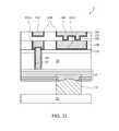
- FIG. 21illustrates the formation of damascene structures including metal lines 144 and vias 146 , which may include depositing conductive barrier layer 148 (for example, a Ti layer), plating copper, and performing a CMP to remove excess copper.
- FIGS. 22 through 23Aillustrate the formation of dielectric layer 38 and bump 42 . The formation processes may be essentially the same as described in the preceding embodiment, and hence are not repeated herein.
- FIG. 23Billustrates an alternative embodiment, wherein metal lines 144 and vias 146 are formed in dielectric layer 124 .
- FIGS. 24 through 29Billustrate yet another embodiment.
- the initial steps of this embodimentare the same as shown in FIGS. 1 and 2 .
- etch stop layer 220is formed.
- etch stop layer 220is formed of silicon nitride, and may have a thickness, for example, of about 750 ⁇ .
- Dielectric layer 222is then formed on etch stop layer 220 .
- dielectric layer 222is formed using one of various chemical vapor deposition (CVD) methods, and may comprise, for example, an oxide. The thickness of the CVD dielectric layer 222 may be, for example, about 8 K ⁇ .
- CVDchemical vapor deposition
- dielectric layer 222may be formed of polyimide, and hence may have a significantly greater thickness than what is formed using CVD.
- the thickness of dielectric layer 222 formed of polyimidemay be greater than about 2 ⁇ m, and may be about 5 ⁇ m in an exemplary embodiment.
- FIGS. 25 through 27illustrate the formation of via opening 226 and trench openings 228 .
- the formation detailsare essentially the same as illustrated in FIGS. 18 through 20 , and hence are not repeated herein.
- a dual damascene structureincluding vias 232 and overlying metal lines 234 , which may be formed of copper, are formed.
- Conductive barrier layers 236are also formed.
- FIG. 29Aillustrates the formation of dielectric layer 38 and bump 42 .
- the materials and the formation processes of dielectric layer 38 and bump 42may be essentially the same as illustrated in FIGS. 10-12A .
- FIG. 29Billustrates an alternative embodiment with an additional layer of interconnection ( 60 ), which includes additional dual damascene structures. If necessary, more interconnection layers may be inserted
- the embodimentshave several advantageous features.
- the metal padsBy recessing substrates to form metal pads ( 36 - 2 in FIGS. 10 and 132 - 1 in FIG. 17 ) to contact TSVs, the metal pads may have great sizes, so that the accuracy requirement in the alignment of the metal pads to TSVs is relaxed. Further, the metal pads and the underlying TSVs have large contact areas, and hence the contact resistances are reduced.
Landscapes
- Engineering & Computer Science (AREA)
- Computer Hardware Design (AREA)
- Microelectronics & Electronic Packaging (AREA)
- Power Engineering (AREA)
- Manufacturing & Machinery (AREA)
- Physics & Mathematics (AREA)
- Condensed Matter Physics & Semiconductors (AREA)
- General Physics & Mathematics (AREA)
- Internal Circuitry In Semiconductor Integrated Circuit Devices (AREA)
- Wire Bonding (AREA)
Abstract
Description
This application claims the benefit of U.S. Provisional Application No. 61/244,773 filed on Sep. 22, 2009, entitled “Wafer Backside Interconnect Structure Connected to TSVs,” which application is hereby incorporated herein by reference.
This disclosure relates generally to integrated circuit structures, and more particularly to interconnect structures formed on the backside of wafers and connected to through-substrate vias.
The semiconductor industry has experienced continuous rapid growth due to constant improvements in the integration density of various electronic components (i.e., transistors, diodes, resistors, capacitors, etc.). For the most part, this improvement in integration density has come from repeated reductions in minimum feature size, allowing more components to be integrated into a given chip area.
These integration improvements are essentially two-dimensional (2D) in nature, in that the volume occupied by the integrated components is essentially on the surface of the semiconductor wafer. Although dramatic improvements in lithography have resulted in considerable improvements in 2D integrated circuit formation, there are physical limitations to the density that can be achieved in two dimensions. One of these limitations is the minimum size needed to make these components. Also, when more devices are put into one chip, more complex designs are required.
An additional limitation comes from the significant increase in the number and lengths of interconnections between devices as the number of devices increases. When the number and the lengths of interconnections increase, both circuit RC delay and power consumption increase.
Among the efforts for resolving the above-discussed limitations, three-dimensional integrated circuit (3D IC) and stacked dies are commonly used. Through-substrate vias (TSVs) are thus used in 3D ICs and stacked dies for connecting dies. In this case, TSVs are often used to connect the integrated circuits on a die to the backside of the die. In addition, TSVs are also used to provide short grounding paths for grounding the integrated circuits through the backside of the die, which may be covered by a grounded metallic film.
Since the bonding of chips comprising TSVs requires relatively large pitch between TSVs, the location of the TSVs is restricted and the distance between the TSVs needs to be big enough to allow room for, for example, solder balls. In addition, with the existing methods for forming wafer backside structures, it is impossible to route the electrical connection of TSVs to locations far away from the respective TSVs.
In accordance with one aspect of the embodiment, an integrated circuit structure includes a semiconductor substrate having a front surface and a back surface; a conductive via passing through the semiconductor substrate; and a metal feature on the back surface of the semiconductor substrate. The metal feature includes a metal pad overlying and contacting the conductive via, and a metal line over the conductive via. The metal line includes a dual damascene structure. The integrated circuit structure further includes a bump overlying the metal line.
Other embodiments are also disclosed.
For a more complete understanding of the disclosure, and the advantages thereof, reference is now made to the following descriptions taken in conjunction with the accompanying drawings, in which:
The making and using of the embodiments of the disclosure are discussed in detail below. It should be appreciated, however, that the embodiments provide many applicable inventive concepts that can be embodied in a wide variety of specific contexts. The specific embodiments discussed are merely illustrative of specific ways to make and use the invention, and do not limit the scope of the invention.
A novel backside connection structure connected to through-substrate vias (TSVs) and the method of forming the same are provided. The intermediate stages of manufacturing an embodiment are illustrated. The variations of the embodiment are discussed. Throughout the various views and illustrative embodiments, like reference numbers are used to designate like elements.
Referring toFIG. 1 ,chip 2, which includessubstrate 10 and integrated circuits (not shown) therein, is provided.Chip 2 may be a portion of a wafer.Substrate 10 may be a semiconductor substrate, such as a bulk silicon substrate, although it may include other semiconductor materials such as group III, group IV, and/or group V elements. Active semiconductor devices such as transistors (symbolized by block15) may be formed onfront side 10fofsubstrate 10. Throughout the description, the term “backside” refers to the side ofsubstrate 10 opposite the side having the active semiconductor devices.Interconnect structure 12, which includes metal lines and vias (not shown) formed therein, is formed onfront side 10fofsubstrate 10 and connected to the active semiconductor devices. The metal lines and vias may be formed of copper or copper alloys, and may be formed using the well-known damascene processes.Interconnect structure 12 may include commonly known inter-layer dielectric (ILD) and inter-metal dielectrics (IMDs).Bond pad 14 is formed on thefront side 10fofsubstrate 10.
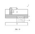
Referring toFIG. 2 , a backside grinding is performed so thatTSV 20 is exposed through theback surface 10bofsubstrate 10. The backside grinding may be performed usingTSV 20 as a stop layer. Next, as shown inFIG. 3 ,TSV 20 is recessed, so that it's top surface is lower than theback surface 10bofsubstrate 10. The recess depth D1 may be greater than about 0.5 μm, and may be 3 μm in an exemplary embodiment. As a result of the recessing, opening24 is formed.
Referring toFIG. 5 ,dielectric isolation layer 30 is deposited. The deposition methods include low-temperature chemical vapor deposition (LTCVD), although other commonly used methods may also be used. In an exemplary embodiment,dielectric isolation layer 30 comprises silicon nitride (SiNx), and may have a thickness of a several hundred angstroms. Next, as shown inFIG. 6 , a portion of thedielectric isolation layer 30 overlying the end of theTSV 20 is exposed in a viaopening 33 by applying photo resist31 and performing photolithography processes, so that the subsequently formed bump may be electrically connected toTSV 20.
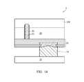
Referring toFIG. 14 ,dielectric layer 124 is formed on the back surface ofsubstrate 10 and coversTSV 20. In an embodiment,dielectric layer 124 is formed of polyimide, and may have a thickness greater than about 2 μm, with an exemplary thickness equal to about 3 μm. In alternative embodiments, other dielectric materials may be used.
Referring toFIG. 16 , a pre-clean is performed, andconductive barrier layer 128 is deposited, for example, by sputtering.Conductive barrier layer 128 may comprise titanium, tantalum, or the like.Metallic material 130 is then plated to a level higher than the top surface ofdielectric layer 124.Metallic material 130 may include copper, although other metals such as aluminum, tungsten, or the like, may also be used. A CMP is then performed, as shown inFIG. 17 , and hence metal lines/pads132 (denoted as132-1 and132-2) are formed. Metal line132-2 may be electrically connected to one of the TSVs in the chip. Accordingly, metal line132-2 may be used as a redistribution line. Metal feature132-1 may be a metal pad or a metal trace. The metal pad may have dimensions (viewed from top) greater than that ofTSV 20, wherein in the top view, metal pad132-1 may extend beyond the edges ofTSV 20 in all lateral directions.
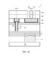
Referring toFIG. 19 , photo resist134 is removed, and an additional photo resist140 is formed and patterned. Trenchopenings 138 are then formed by furtheretching dielectric layer 125 through patterned photo resist140, as illustrated inFIG. 20 . The etching may be performed using a time mode, so that the etching is stopped at an intermediate level ofdielectric layer 125. Photo resist140 is then removed, for example, by ashing. It is realized that the steps shown inFIGS. 18 through 20 are a via-first approach, in which viaopenings 136 are formed before the formation oftrench openings 138. One skilled in the art will realize that the structure shown inFIG. 20 may be formed using a trench-first approach, in which the steps shown inFIGS. 19 and 20 may be performed before the step shown inFIG. 18 .
The embodiments have several advantageous features. By forming backside interconnect structures using dual damascene processes, multiple interconnect layers may be stacked to provide a great routing ability. By recessing substrates to form metal pads (36-2 in FIGS.10 and132-1 inFIG. 17 ) to contact TSVs, the metal pads may have great sizes, so that the accuracy requirement in the alignment of the metal pads to TSVs is relaxed. Further, the metal pads and the underlying TSVs have large contact areas, and hence the contact resistances are reduced.
Although the embodiments and their advantages have been described in detail, it should be understood that various changes, substitutions and alterations can be made herein without departing from the spirit and scope of the invention as defined by the appended claims. Moreover, the scope of the present application is not intended to be limited to the particular embodiments of the process, machine, manufacture, and composition of matter, means, methods and steps described in the specification. As one of ordinary skill in the art will readily appreciate from the disclosure of the present invention, processes, machines, manufacture, compositions of matter, means, methods, or steps, presently existing or later to be developed, that perform substantially the same function or achieve substantially the same result as the corresponding embodiments described herein may be utilized according to the present invention. Accordingly, the appended claims are intended to include within their scope such processes, machines, manufacture, compositions of matter, means, methods, or steps. In addition, each claim constitutes a separate embodiment, and the combination of various claims and embodiments are within the scope of the invention.
Claims (19)
1. An integrated circuit structure comprising:
a semiconductor substrate having an active semiconductor device formed on a first side of the semiconductor substrate;
a conductive via passing through the semiconductor substrate;
a metal feature on a second side of the semiconductor substrate opposing the first side of the semiconductor substrate, the metal feature comprising:
a metal pad overlying and contacting the conductive via, wherein from a top-down perspective, all horizontal dimensions of the metal pad are greater than respective horizontal dimensions of the conductive via; and
a metal line higher than the conductive via, relative the second side of the semiconductor substrate, wherein the metal line comprises a dual damascene structure; and
a bump overlying the metal line.
2. The integrated circuit structure ofclaim 1 , wherein the metal pad further comprises:
a first bottom surface contacting a conductive barrier layer, wherein the conductive barrier layer contacts a top surface of the conductive via; and
a second bottom surface higher than the second side of the semiconductor substrate and lower than the first bottom surface.
3. The integrated circuit structure ofclaim 1 , wherein the dual damascene structure is in a same dielectric layer as the metal pad.
4. The integrated circuit structure ofclaim 1 , wherein the dual damascene structure is in a dielectric layer over the metal pad.
5. The integrated circuit structure ofclaim 1 further comprising a polyimide layer, wherein the metal pad is in the polyimide layer.
6. The integrated circuit structure ofclaim 1 , wherein the metal feature further comprises a conductive barrier layer.
7. An integrated circuit structure comprising:
a semiconductor substrate having a front side and a backside, wherein the backside is opposite the front side;
an active device formed on the front side;
a through-substrate via (TSV) penetrating through the semiconductor substrate;
a first dielectric layer on the backside of the semiconductor substrate, wherein the dielectric layer comprises a metal pad overlying the TSV, wherein from a top-down perspective, all horizontal dimensions of the metal pad are greater than respective horizontal dimensions of the TSV; and
a second dielectric layer on the backside of the semiconductor substrate and over the first dielectric layer relative the backside of the semiconductor substrate, the second dielectric layer comprises a first metal line, wherein the first metal line comprises a dual-damascene structure.
8. The integrated circuit structure ofclaim 7 , wherein the metal pad comprises a conductive barrier layer.
9. The integrated circuit structure ofclaim 7 , wherein the first metal line further comprises a conductive barrier layer.
10. The integrated circuit structure ofclaim 7 , wherein the second dielectric layer further comprises a second metal line, the second metal line comprising a single damascene structure.
11. The integrated circuit structure ofclaim 7 , wherein the TSV comprises a portion penetrating into the first dielectric layer.
12. The integrated circuit structure ofclaim 7 , further comprising an isolation layer covering at least a portion of sidewalls of the TSV.
13. The integrated circuit structure ofclaim 7 , wherein the first dielectric layer comprises a portion between the metal pad and the semiconductor substrate.
14. The integrated circuit structure ofclaim 7 , further comprising a bump overlying the first metal line.
15. The integrated circuit structure ofclaim 7 , wherein the metal pad comprises:
a first bottom surface contacting a top surface of the TSV; and
a second bottom surface higher than the backside of the semiconductor substrate and lower than the first bottom surface.
16. An integrated circuit structure comprising:
a semiconductor substrate having a front side and a backside, wherein the backside is opposite the front side;
an active device formed on the front side;
a through-substrate via (TSV) penetrating through the semiconductor substrate; and
a dielectric layer on the backside of the semiconductor substrate, wherein the dielectric layer comprises:
a metal pad overlying the TSV, wherein from a top-down perspective, all horizontal dimensions of the metal pad are greater than respective horizontal dimensions of the TSV; and
a metal line, wherein the metal line comprises a dual-damascene structure.
17. The integrated circuit structure ofclaim 14 , wherein the metal pad and the metal line comprise a conductive barrier layer, respectively.
18. The integrated circuit structure ofclaim 14 , further comprising a bump overlying the metal line.
19. The integrated circuit structure ofclaim 16 , wherein the metal pad comprises:
a first bottom surface contacting a top surface of the TSV; and
a second bottom surface higher than the backside of the semiconductor substrate and lower than the first bottom surface.
Priority Applications (8)
| Application Number | Priority Date | Filing Date | Title |
|---|---|---|---|
| US12/832,019US8791549B2 (en) | 2009-09-22 | 2010-07-07 | Wafer backside interconnect structure connected to TSVs |
| KR1020100080460AKR101319701B1 (en) | 2009-09-22 | 2010-08-19 | Wafer Backside Interconnect Structure Connected To TSVs |
| TW099130601ATWI453879B (en) | 2009-09-22 | 2010-09-10 | Integrated circuit structure |
| CN2010102837900ACN102024781B (en) | 2009-09-22 | 2010-09-14 | 3D integrated circuit structure |
| JP2010211576AJP5271985B2 (en) | 2009-09-22 | 2010-09-22 | Integrated circuit structure |
| US14/323,677US9449875B2 (en) | 2009-09-22 | 2014-07-03 | Wafer backside interconnect structure connected to TSVs |
| US14/323,617US9716074B2 (en) | 2009-09-22 | 2014-07-03 | Wafer backside interconnect structure connected to TSVs |
| US15/269,613US9978708B2 (en) | 2009-09-22 | 2016-09-19 | Wafer backside interconnect structure connected to TSVs |
Applications Claiming Priority (2)
| Application Number | Priority Date | Filing Date | Title |
|---|---|---|---|
| US24477309P | 2009-09-22 | 2009-09-22 | |
| US12/832,019US8791549B2 (en) | 2009-09-22 | 2010-07-07 | Wafer backside interconnect structure connected to TSVs |
Related Child Applications (2)
| Application Number | Title | Priority Date | Filing Date |
|---|---|---|---|
| US14/323,617DivisionUS9716074B2 (en) | 2009-09-22 | 2014-07-03 | Wafer backside interconnect structure connected to TSVs |
| US14/323,677ContinuationUS9449875B2 (en) | 2009-09-22 | 2014-07-03 | Wafer backside interconnect structure connected to TSVs |
Publications (2)
| Publication Number | Publication Date |
|---|---|
| US20110068466A1 US20110068466A1 (en) | 2011-03-24 |
| US8791549B2true US8791549B2 (en) | 2014-07-29 |
Family
ID=43755919
Family Applications (4)
| Application Number | Title | Priority Date | Filing Date |
|---|---|---|---|
| US12/832,019Active2031-10-07US8791549B2 (en) | 2009-09-22 | 2010-07-07 | Wafer backside interconnect structure connected to TSVs |
| US14/323,677ActiveUS9449875B2 (en) | 2009-09-22 | 2014-07-03 | Wafer backside interconnect structure connected to TSVs |
| US14/323,617ActiveUS9716074B2 (en) | 2009-09-22 | 2014-07-03 | Wafer backside interconnect structure connected to TSVs |
| US15/269,613Active2030-09-08US9978708B2 (en) | 2009-09-22 | 2016-09-19 | Wafer backside interconnect structure connected to TSVs |
Family Applications After (3)
| Application Number | Title | Priority Date | Filing Date |
|---|---|---|---|
| US14/323,677ActiveUS9449875B2 (en) | 2009-09-22 | 2014-07-03 | Wafer backside interconnect structure connected to TSVs |
| US14/323,617ActiveUS9716074B2 (en) | 2009-09-22 | 2014-07-03 | Wafer backside interconnect structure connected to TSVs |
| US15/269,613Active2030-09-08US9978708B2 (en) | 2009-09-22 | 2016-09-19 | Wafer backside interconnect structure connected to TSVs |
Country Status (5)
| Country | Link |
|---|---|
| US (4) | US8791549B2 (en) |
| JP (1) | JP5271985B2 (en) |
| KR (1) | KR101319701B1 (en) |
| CN (1) | CN102024781B (en) |
| TW (1) | TWI453879B (en) |
Cited By (13)
| Publication number | Priority date | Publication date | Assignee | Title |
|---|---|---|---|---|
| US20150179580A1 (en)* | 2013-12-24 | 2015-06-25 | United Microelectronics Corp. | Hybrid interconnect structure and method for fabricating the same |
| US9343361B2 (en) | 2010-11-29 | 2016-05-17 | Samsung Electronics Co., Ltd. | Semiconductor device, fabricating method thereof and semiconductor package including the semiconductor device |
| US9449913B2 (en) | 2011-10-28 | 2016-09-20 | Intel Corporation | 3D interconnect structure comprising fine pitch single damascene backside metal redistribution lines combined with through-silicon vias |
| US9728490B2 (en) | 2015-08-24 | 2017-08-08 | Samsung Electronics Co., Ltd. | Semiconductor devices and methods of manufacturing the same |
| US20180315620A1 (en)* | 2017-04-28 | 2018-11-01 | Samsung Electronics Co., Ltd. | Semiconductor device and method for manufacturing the same |
| US20190259725A1 (en)* | 2017-07-21 | 2019-08-22 | United Microelectronics Corp. | Manufacturing method of die-stack structure |
| US10586824B2 (en) | 2017-10-30 | 2020-03-10 | Samsung Electronics Co., Ltd. | Image sensor |
| US11195810B2 (en)* | 2019-08-23 | 2021-12-07 | Taiwan Semiconductor Manufacturing Company, Ltd. | Bonding structure and method of forming same |
| US20220157694A1 (en)* | 2018-07-31 | 2022-05-19 | Intel Corporation | Micro through-silicon via for transistor density scaling |
| US20220302053A1 (en)* | 2021-03-17 | 2022-09-22 | Samsung Electronics Co., Ltd. | Interposer, method for fabricating the same, and semiconductor package having the same |
| US11521923B2 (en)* | 2018-05-24 | 2022-12-06 | Intel Corporation | Integrated circuit package supports |
| US20230087718A1 (en)* | 2021-09-03 | 2023-03-23 | Samsung Electronics Co., Ltd. | Method of manufacturing semiconductor device using gas blowing agent |
| US11843020B2 (en) | 2017-10-30 | 2023-12-12 | Samsung Electronics Co., Ltd. | Image sensor |
Families Citing this family (59)
| Publication number | Priority date | Publication date | Assignee | Title |
|---|---|---|---|---|
| US8513119B2 (en) | 2008-12-10 | 2013-08-20 | Taiwan Semiconductor Manufacturing Company, Ltd. | Method of forming bump structure having tapered sidewalls for stacked dies |
| US20100171197A1 (en)* | 2009-01-05 | 2010-07-08 | Hung-Pin Chang | Isolation Structure for Stacked Dies |
| US8791549B2 (en) | 2009-09-22 | 2014-07-29 | Taiwan Semiconductor Manufacturing Company, Ltd. | Wafer backside interconnect structure connected to TSVs |
| US8466059B2 (en) | 2010-03-30 | 2013-06-18 | Taiwan Semiconductor Manufacturing Company, Ltd. | Multi-layer interconnect structure for stacked dies |
| US8716867B2 (en) | 2010-05-12 | 2014-05-06 | Taiwan Semiconductor Manufacturing Company, Ltd. | Forming interconnect structures using pre-ink-printed sheets |
| US9190325B2 (en)* | 2010-09-30 | 2015-11-17 | Taiwan Semiconductor Manufacturing Company, Ltd. | TSV formation |
| KR101789765B1 (en)* | 2010-12-16 | 2017-11-21 | 삼성전자주식회사 | Semiconductor device and method of forming the same |
| KR20120090417A (en)* | 2011-02-08 | 2012-08-17 | 삼성전자주식회사 | Semiconductor device and method of manufacturing a semiconductor device |
| US8853072B2 (en)* | 2011-06-06 | 2014-10-07 | Micron Technology, Inc. | Methods of forming through-substrate interconnects |
| JP2012256679A (en)* | 2011-06-08 | 2012-12-27 | Elpida Memory Inc | Semiconductor device and manufacturing method of the same |
| US8900994B2 (en) | 2011-06-09 | 2014-12-02 | Taiwan Semiconductor Manufacturing Company, Ltd. | Method for producing a protective structure |
| CN103000571B (en)* | 2011-09-19 | 2015-07-08 | 中芯国际集成电路制造(上海)有限公司 | Semiconductor device and manufacturing method thereof |
| US9142510B2 (en) | 2011-10-28 | 2015-09-22 | Intel Corporation | 3D interconnect structure comprising through-silicon vias combined with fine pitch backside metal redistribution lines fabricated using a dual damascene type approach |
| US20130313710A1 (en)* | 2012-05-22 | 2013-11-28 | Micron Technology, Inc. | Semiconductor Constructions and Methods of Forming Semiconductor Constructions |
| KR101931115B1 (en) | 2012-07-05 | 2018-12-20 | 삼성전자주식회사 | Semiconductor device and method of forming the same |
| KR20140023055A (en)* | 2012-08-16 | 2014-02-26 | 에스케이하이닉스 주식회사 | Semiconductor device and method for forming using the same |
| KR102021884B1 (en)* | 2012-09-25 | 2019-09-18 | 삼성전자주식회사 | Semiconductor Device Having Backside Bonding Structure |
| US8859425B2 (en) | 2012-10-15 | 2014-10-14 | Micron Technology, Inc. | Devices, systems, and methods related to forming through-substrate vias with sacrificial plugs |
| KR102018885B1 (en)* | 2012-12-20 | 2019-09-05 | 삼성전자주식회사 | Semiconductor devices having through vias and methods for fabricating the same |
| US10483132B2 (en)* | 2012-12-28 | 2019-11-19 | Taiwan Semiconductor Manufacturing Company, Ltd. | Post-passivation interconnect structure and method of forming the same |
| US9466578B2 (en)* | 2013-12-20 | 2016-10-11 | Qualcomm Incorporated | Substrate comprising improved via pad placement in bump area |
| US9093503B1 (en)* | 2014-01-03 | 2015-07-28 | International Business Machines Corporation | Semiconductor chip with a dual damascene wire and through-substrate via (TSV) structure |
| US9865523B2 (en)* | 2014-01-17 | 2018-01-09 | Taiwan Semiconductor Manufacturing Company, Ltd. | Robust through-silicon-via structure |
| KR102222485B1 (en)* | 2014-09-18 | 2021-03-04 | 에스케이하이닉스 주식회사 | Semiconductor device having through via, semiconductor package including the same and the method for manufacturing semiconductor device |
| DE102014115105B4 (en) | 2014-10-09 | 2023-06-22 | Taiwan Semiconductor Manufacturing Company, Ltd. | Semiconductor device and method of manufacturing a semiconductor device |
| TWI582918B (en)* | 2014-11-12 | 2017-05-11 | 精材科技股份有限公司 | Chip package and manufacturing method thereof |
| KR102279729B1 (en)* | 2014-12-01 | 2021-07-21 | 삼성전자주식회사 | Semiconductor Devices Having a TSV, a Frontside Bumping Pad, and a Backside Bumping Pad |
| US9431343B1 (en) | 2015-03-11 | 2016-08-30 | Samsung Electronics Co., Ltd. | Stacked damascene structures for microelectronic devices |
| US9666523B2 (en) | 2015-07-24 | 2017-05-30 | Nxp Usa, Inc. | Semiconductor wafers with through substrate vias and back metal, and methods of fabrication thereof |
| US9472490B1 (en) | 2015-08-12 | 2016-10-18 | GlobalFoundries, Inc. | IC structure with recessed solder bump area and methods of forming same |
| US10121812B2 (en)* | 2015-12-29 | 2018-11-06 | Taiwan Semiconductor Manufacturing Co., Ltd. | Stacked substrate structure with inter-tier interconnection |
| US10276402B2 (en)* | 2016-03-21 | 2019-04-30 | Taiwan Semiconductor Manufacturing Co., Ltd. | Semiconductor package and manufacturing process thereof |
| JP6955864B2 (en)* | 2016-12-26 | 2021-10-27 | ラピスセミコンダクタ株式会社 | Semiconductor devices and methods for manufacturing semiconductor devices |
| KR102489216B1 (en)* | 2017-01-20 | 2023-01-16 | 도쿄엘렉트론가부시키가이샤 | Interconnection structure and method of forming the same |
| US10515921B2 (en)* | 2017-07-27 | 2019-12-24 | Taiwan Semiconductor Manufacturing Co., Ltd. | Semiconductor package and method of fabricating semiconductor package |
| US10636758B2 (en)* | 2017-10-05 | 2020-04-28 | Texas Instruments Incorporated | Expanded head pillar for bump bonds |
| KR102665246B1 (en)* | 2018-07-03 | 2024-05-09 | 삼성전자주식회사 | Semiconductor device and method for fabricating thereof |
| KR102635832B1 (en) | 2018-09-28 | 2024-02-15 | 삼성전자주식회사 | Semiconductor device and method of fabricating the same |
| US10727124B2 (en) | 2018-10-29 | 2020-07-28 | International Business Machines Corporation | Structure and method for forming fully-aligned trench with an up-via integration scheme |
| JP7353748B2 (en)* | 2018-11-29 | 2023-10-02 | キヤノン株式会社 | Semiconductor device manufacturing method and semiconductor device |
| US10770427B1 (en)* | 2019-06-27 | 2020-09-08 | Taiwan Semiconductor Manufacturing Co., Ltd. | Chip package structure and method for forming the same |
| US11398408B2 (en)* | 2019-09-24 | 2022-07-26 | Advanced Semiconductor Engineering, Inc. | Semiconductor substrate with trace connected to via at a level within a dielectric layer |
| US11094580B2 (en)* | 2019-10-01 | 2021-08-17 | International Business Machines Corporation | Structure and method to fabricate fully aligned via with reduced contact resistance |
| US11217481B2 (en)* | 2019-11-08 | 2022-01-04 | International Business Machines Corporation | Fully aligned top vias |
| US11295978B2 (en) | 2020-04-29 | 2022-04-05 | International Business Machines Corporation | Interconnects having spacers for improved top via critical dimension and overlay tolerance |
| KR20210133524A (en) | 2020-04-29 | 2021-11-08 | 삼성전자주식회사 | Interconnection structure and Semiconductor package including the same |
| US11404378B2 (en)* | 2020-11-24 | 2022-08-02 | Omnivision Technologies, Inc. | Semiconductor device with buried metal pad, and methods for manufacture |
| US12205997B2 (en)* | 2021-03-12 | 2025-01-21 | Taiwan Semiconductor Manufacturing Co., Ltd. | Integrated circuit including backside conductive vias |
| US12300492B2 (en) | 2021-03-26 | 2025-05-13 | Changxin Memory Technologies, Inc. | Method for manufacturing semiconductor structure, and semiconductor structure |
| US12100670B2 (en) | 2021-03-26 | 2024-09-24 | Changxin Memory Technologies, Inc. | Method for manufacturing semiconductor structure and semiconductor structure |
| CN113078119B (en)* | 2021-03-26 | 2022-03-18 | 长鑫存储技术有限公司 | Manufacturing method of semiconductor structure and semiconductor structure |
| KR20220167423A (en) | 2021-06-11 | 2022-12-21 | 삼성전자주식회사 | Semiconductor device including through electrodes |
| US12176311B2 (en)* | 2021-07-05 | 2024-12-24 | Changxin Memory Technologies, Inc. | Micro bump, method for forming micro bump, chip interconnection structure and chip interconnection method |
| US12087691B2 (en) | 2021-09-21 | 2024-09-10 | International Business Machines Corporation | Semiconductor structures with backside gate contacts |
| KR102681185B1 (en)* | 2021-09-24 | 2024-07-04 | 한국기계연구원 | Micro-led display panel and method for manufacturing the same |
| US12002758B2 (en) | 2021-11-04 | 2024-06-04 | International Business Machines Corporation | Backside metal-insulator-metal (MIM) capacitors extending through backside interlayer dielectric (BILD) layer or semiconductor layer and partly through dielectric layer |
| US20230378016A1 (en)* | 2022-05-23 | 2023-11-23 | Taiwan Semiconductor Manufacturing Company, Ltd. | Techniques for heat dispersion in 3d integrated circuit |
| KR20240019456A (en)* | 2022-08-04 | 2024-02-14 | 삼성전자주식회사 | Semiconductor device |
| CN119008562B (en)* | 2024-10-23 | 2024-12-27 | 湖北星辰技术有限公司 | Semiconductor device, manufacturing method thereof and memory system |
Citations (98)
| Publication number | Priority date | Publication date | Assignee | Title |
|---|---|---|---|---|
| US5391917A (en) | 1993-05-10 | 1995-02-21 | International Business Machines Corporation | Multiprocessor module packaging |
| US5426072A (en)* | 1993-01-21 | 1995-06-20 | Hughes Aircraft Company | Process of manufacturing a three dimensional integrated circuit from stacked SOI wafers using a temporary silicon substrate |
| US5510298A (en) | 1991-09-12 | 1996-04-23 | Texas Instruments Incorporated | Method of interconnect in an integrated circuit |
| US5646067A (en) | 1995-06-05 | 1997-07-08 | Harris Corporation | Method of bonding wafers having vias including conductive material |
| US5767001A (en) | 1993-05-05 | 1998-06-16 | Siemens Aktiengesellschaft | Process for producing semiconductor components between which contact is made vertically |
| US5998292A (en) | 1997-11-12 | 1999-12-07 | International Business Machines Corporation | Method for making three dimensional circuit integration |
| US6034436A (en)* | 1996-11-28 | 2000-03-07 | Nec Corporation | Semiconductor device having an improved through-hole structure |
| US6184060B1 (en) | 1996-10-29 | 2001-02-06 | Trusi Technologies Llc | Integrated circuits and methods for their fabrication |
| US6322903B1 (en) | 1999-12-06 | 2001-11-27 | Tru-Si Technologies, Inc. | Package of integrated circuits and vertical integration |
| US20020084513A1 (en) | 1996-10-29 | 2002-07-04 | Oleg Siniaguine | Integrated circuits and methods for their fabrication |
| US6417087B1 (en)* | 1999-12-16 | 2002-07-09 | Agere Systems Guardian Corp. | Process for forming a dual damascene bond pad structure over active circuitry |
| US20020113321A1 (en) | 2001-02-22 | 2002-08-22 | Oleg Siniaguine | Devices having substrates with opening passing through the substrates and conductors in the openings, and methods of manufacture |
| US6448168B1 (en) | 1997-09-30 | 2002-09-10 | Intel Corporation | Method for distributing a clock on the silicon backside of an integrated circuit |
| US6451684B1 (en) | 1998-07-21 | 2002-09-17 | Samsung Electronics Co., Ltd. | Semiconductor device having a conductive layer side surface slope which is at least 90° and method for manufacturing the same |
| US6465892B1 (en) | 1999-04-13 | 2002-10-15 | Oki Electric Industry Co., Ltd. | Interconnect structure for stacked semiconductor device |
| US20020182855A1 (en)* | 2001-06-01 | 2002-12-05 | Agarwala Birendra N. | Dual damascene multi-level metallization |
| US6498381B2 (en) | 2001-02-22 | 2002-12-24 | Tru-Si Technologies, Inc. | Semiconductor structures having multiple conductive layers in an opening, and methods for fabricating same |
| US6538333B2 (en) | 2000-06-16 | 2003-03-25 | Chartered Semiconductor Manufacturing Ltd. | Three dimensional IC package module |
| TW531892B (en) | 2000-04-05 | 2003-05-11 | Hitachi Ltd | Semiconductor integrated circuit device and fabrication method for semiconductor integrated circuit device |
| US6599778B2 (en) | 2001-12-19 | 2003-07-29 | International Business Machines Corporation | Chip and wafer integration process using vertical connections |
| US20030148600A1 (en) | 1999-07-01 | 2003-08-07 | Hitachi, Ltd. | Method of forming conductive layers in the trenches or through holes made in an insulating film on a semiconductor substrate |
| US20040048459A1 (en)* | 2002-04-11 | 2004-03-11 | Robert Patti | Interlocking conductor method for bonding wafers to produce stacked integrated circuits |
| US20040188822A1 (en) | 2003-01-15 | 2004-09-30 | Kazumi Hara | Semiconductor chip, semiconductor wafer, semiconductor device and method of manufacturing the same, circuit board, and electronic instrument |
| US6800930B2 (en) | 2002-07-31 | 2004-10-05 | Micron Technology, Inc. | Semiconductor dice having back side redistribution layer accessed using through-silicon vias, and assemblies |
| US20040248398A1 (en)* | 2001-03-15 | 2004-12-09 | Micron Technology, Inc. | Barrier-metal-free copper damascene technology using atomic hydrogen enhanced reflow |
| US20040245623A1 (en) | 2003-03-28 | 2004-12-09 | Kazumi Hara | Semiconductor device, circuit substrate and electronic instrument |
| US6841883B1 (en) | 2003-03-31 | 2005-01-11 | Micron Technology, Inc. | Multi-dice chip scale semiconductor components and wafer level methods of fabrication |
| US6873054B2 (en) | 2002-04-24 | 2005-03-29 | Seiko Epson Corporation | Semiconductor device and a method of manufacturing the same, a circuit board and an electronic apparatus |
| US6897125B2 (en) | 2003-09-17 | 2005-05-24 | Intel Corporation | Methods of forming backside connections on a wafer stack |
| US6908856B2 (en) | 2003-04-03 | 2005-06-21 | Interuniversitair Microelektronica Centrum (Imec) | Method for producing electrical through hole interconnects and devices made thereof |
| US6914336B2 (en) | 2000-01-25 | 2005-07-05 | Nec Electronics Corporation | Semiconductor device structure and method for manufacturing the same |
| US6924551B2 (en) | 2003-05-28 | 2005-08-02 | Intel Corporation | Through silicon via, folded flex microelectronic package |
| US20050194691A1 (en)* | 2004-03-08 | 2005-09-08 | Fujitsu Limited | Method of forming wiring structure and semiconductor device |
| US20050200025A1 (en)* | 2003-11-21 | 2005-09-15 | International Business Machines Corporation | Low-k dielectric material system for IC application |
| US20050221601A1 (en)* | 2004-03-31 | 2005-10-06 | Nec Electronics Corporation | Semiconductor device and method for manufacturing the same |
| US20050233581A1 (en)* | 2004-03-31 | 2005-10-20 | Nec Electronics Corporation | Method for manufacturing semiconductor device |
| US6962872B2 (en) | 2002-12-09 | 2005-11-08 | International Business Machines Corporation | High density chip carrier with integrated passive devices |
| US7049170B2 (en)* | 2003-12-17 | 2006-05-23 | Tru-Si Technologies, Inc. | Integrated circuits and packaging substrates with cavities, and attachment methods including insertion of protruding contact pads into cavities |
| KR20060054690A (en) | 2004-11-16 | 2006-05-23 | 강준모 | Semiconductor device having rear input / output terminal and manufacturing method thereof |
| KR20060054688A (en) | 2004-11-16 | 2006-05-23 | 강준모 | Semiconductor device having rear input / output terminal and manufacturing method thereof |
| KR20060054689A (en) | 2004-11-16 | 2006-05-23 | 강준모 | Semiconductor device having rear input / output terminal and manufacturing method thereof |
| US7053465B2 (en) | 2000-11-28 | 2006-05-30 | Texas Instruments Incorporated | Semiconductor varactor with reduced parasitic resistance |
| US7060601B2 (en)* | 2003-12-17 | 2006-06-13 | Tru-Si Technologies, Inc. | Packaging substrates for integrated circuits and soldering methods |
| US7071546B2 (en) | 2002-01-16 | 2006-07-04 | Alfred E. Mann Foundation For Scientific Research | Space-saving packaging of electronic circuits |
| US7111149B2 (en) | 2003-07-07 | 2006-09-19 | Intel Corporation | Method and apparatus for generating a device ID for stacked devices |
| US7122912B2 (en) | 2004-01-28 | 2006-10-17 | Nec Electronics Corporation | Chip and multi-chip semiconductor device using thereof and method for manufacturing same |
| US20060273465A1 (en)* | 2005-06-06 | 2006-12-07 | Sharp Kabushiki Kaisha | Semiconductor device and manufacturing method therefor |
| US20060289968A1 (en) | 2005-06-28 | 2006-12-28 | Micron Technology, Inc. | Conductive interconnect structures and formation methods using supercritical fluids |
| US7157787B2 (en) | 2002-02-20 | 2007-01-02 | Intel Corporation | Process of vertically stacking multiple wafers supporting different active integrated circuit (IC) devices |
| US20070032061A1 (en) | 2005-08-05 | 2007-02-08 | Farnworth Warren M | Methods of forming through-wafer interconnects and structures resulting therefrom |
| US20070049016A1 (en) | 2005-09-01 | 2007-03-01 | Micron Technology, Inc. | Microfeature workpieces and methods for forming interconnects in microfeature workpieces |
| US7186343B2 (en) | 1998-10-09 | 2007-03-06 | Zenon Technology Partnership | Cyclic aeration system for submerged membrane modules |
| US7193308B2 (en)* | 2003-09-26 | 2007-03-20 | Seiko Epson Corporation | Intermediate chip module, semiconductor device, circuit board, and electronic device |
| US7262495B2 (en) | 2004-10-07 | 2007-08-28 | Hewlett-Packard Development Company, L.P. | 3D interconnect with protruding contacts |
| TW200737551A (en) | 2005-12-27 | 2007-10-01 | Shinko Electric Ind Co | Semiconductor device and method for manufacturing the same |
| US7297574B2 (en) | 2005-06-17 | 2007-11-20 | Infineon Technologies Ag | Multi-chip device and method for producing a multi-chip device |
| US7300857B2 (en) | 2004-09-02 | 2007-11-27 | Micron Technology, Inc. | Through-wafer interconnects for photoimager and memory wafers |
| US7335972B2 (en) | 2003-11-13 | 2008-02-26 | Sandia Corporation | Heterogeneously integrated microsystem-on-a-chip |
| US20080054444A1 (en) | 2006-08-31 | 2008-03-06 | Micron Technology, Inc. | Microfeature workpieces having interconnects and conductive backplanes, and associated systems and methods |
| US7354798B2 (en)* | 2002-12-20 | 2008-04-08 | International Business Machines Corporation | Three-dimensional device fabrication method |
| US20080136023A1 (en)* | 2006-12-06 | 2008-06-12 | Sony Corporation | Method for manufacturing semiconductor device and semiconductor device |
| US20080211106A1 (en)* | 2007-03-01 | 2008-09-04 | Taiwan Semiconductor Manufacturing Co., Ltd. | Via/contact and damascene structures and manufacturing methods thereof |
| KR20080101635A (en) | 2007-05-18 | 2008-11-21 | 삼성전자주식회사 | Semiconductor package, manufacturing method thereof, and package module and electronic product using semiconductor package |
| JP2009004730A (en) | 2007-06-22 | 2009-01-08 | Ind Technol Res Inst | Self-aligned wafer or chip structure, self-aligned stacked structure, and method of manufacturing the same |
| US20090014843A1 (en) | 2007-06-06 | 2009-01-15 | Kawashita Michihiro | Manufacturing process and structure of through silicon via |
| US20090032966A1 (en)* | 2007-08-01 | 2009-02-05 | Jong Ho Lee | Method of fabricating a 3-D device and device made thereby |
| US20090032960A1 (en) | 2007-07-31 | 2009-02-05 | Micron Technology, Inc. | Semiconductor devices and methods of manufacturing semiconductor devices |
| TW200910557A (en) | 2007-06-20 | 2009-03-01 | Flipchip Int Llc | Under bump metallization structure having a seed layer for electroless nickel deposition |
| US20090057909A1 (en) | 2007-06-20 | 2009-03-05 | Flipchip International, Llc | Under bump metallization structure having a seed layer for electroless nickel deposition |
| US7514775B2 (en) | 2006-10-09 | 2009-04-07 | Taiwan Semiconductor Manufacturing Co., Ltd. | Stacked structures and methods of fabricating stacked structures |
| US20090149023A1 (en) | 2004-08-20 | 2009-06-11 | Zycube Co., Ltd. | Method of fabricating semiconductor device having three-dimensional stacked structure |
| US20090152602A1 (en)* | 2007-12-17 | 2009-06-18 | Kazutaka Akiyama | Semiconductor device and method for manufacturing the same |
| US20090250739A1 (en) | 2008-04-08 | 2009-10-08 | Johnson Jeffrey B | Device Structures with a Hyper-Abrupt P-N Junction, Methods of Forming a Hyper-Abrupt P-N Junction, and Design Structures for an Integrated Circuit |
| US20090269905A1 (en) | 2007-05-16 | 2009-10-29 | Chen-Shien Chen | Tapered Through-Silicon Via Structure |
| US20090283898A1 (en) | 2008-05-15 | 2009-11-19 | Janzen Jeffery W | Disabling electrical connections using pass-through 3d interconnects and associated systems and methods |
| US20090315184A1 (en)* | 2008-05-26 | 2009-12-24 | Oki Semiconductor Co., Ltd. | Semiconductor Device |
| US20100013060A1 (en) | 2008-06-22 | 2010-01-21 | Taiwan Semiconductor Manufacturing Company, Ltd. | Method of forming a conductive trench in a silicon wafer and silicon wafer comprising such trench |
| US20100038800A1 (en) | 2008-08-18 | 2010-02-18 | Samsung Electronics Co., Ltd. | Through-silicon via structures including conductive protective layers and methods of forming the same |
| US20100078770A1 (en)* | 2008-09-26 | 2010-04-01 | International Business Machines Corporation | Lock and Key Through-Via Method for Wafer Level 3 D Integration and Structures Produced |
| US20100127394A1 (en)* | 2008-11-25 | 2010-05-27 | Freescale Semiconductor, Inc. | Through substrate vias for back-side interconnections on very thin semiconductor wafers |
| US20100140805A1 (en) | 2008-12-10 | 2010-06-10 | Hung-Pin Chang | Bump Structure for Stacked Dies |
| US20100171226A1 (en)* | 2008-12-29 | 2010-07-08 | Texas Instruments, Inc. | Ic having tsv arrays with reduced tsv induced stress |
| US20100171197A1 (en)* | 2009-01-05 | 2010-07-08 | Hung-Pin Chang | Isolation Structure for Stacked Dies |
| US20100176494A1 (en) | 2009-01-13 | 2010-07-15 | Ming-Fa Chen | Through-Silicon Via With Low-K Dielectric Liner |
| US7772116B2 (en) | 2005-09-01 | 2010-08-10 | Micron Technology, Inc. | Methods of forming blind wafer interconnects |
| US7772081B2 (en) | 2008-09-17 | 2010-08-10 | Stats Chippac, Ltd. | Semiconductor device and method of forming high-frequency circuit structure and method thereof |
| TW201036106A (en) | 2008-12-23 | 2010-10-01 | Ibm | SOI radio frequency switch with enhanced signal fidelity and electrical isolation |
| US20100330798A1 (en)* | 2009-06-26 | 2010-12-30 | Taiwan Semiconductor Manufacturing Company, Ltd. | Formation of TSV Backside Interconnects by Modifying Carrier Wafers |
| US20110049706A1 (en)* | 2009-09-03 | 2011-03-03 | Taiwan Semiconductor Manufacturing Company, Ltd. | Front Side Copper Post Joint Structure for Temporary Bond in TSV Application |
| US7968460B2 (en) | 2008-06-19 | 2011-06-28 | Micron Technology, Inc. | Semiconductor with through-substrate interconnect |
| US20110165776A1 (en) | 2008-10-09 | 2011-07-07 | Taiwan Semiconductor Manufacturing Company, Ltd. | Bond Pad Connection to Redistribution Lines Having Tapered Profiles |
| US20110186990A1 (en)* | 2010-01-29 | 2011-08-04 | Texas Instruments Incorporated | Protruding tsv tips for enhanced heat dissipation for ic devices |
| US20110233785A1 (en)* | 2010-03-24 | 2011-09-29 | International Business Machines Corporation | Backside dummy plugs for 3d integration |
| US20110241217A1 (en) | 2010-03-30 | 2011-10-06 | Taiwan Semiconductor Manufacturing Company, Ltd. | Multi-Layer Interconnect Structure for Stacked Dies |
| US8058708B2 (en)* | 2007-08-24 | 2011-11-15 | Honda Motor Co., Ltd. | Through hole interconnection structure for semiconductor wafer |
| US8097961B2 (en) | 2007-12-21 | 2012-01-17 | Spansion Llc | Semiconductor device having a simplified stack and method for manufacturing thereof |
| US8174124B2 (en)* | 2010-04-08 | 2012-05-08 | Taiwan Semiconductor Manufacturing Co., Ltd. | Dummy pattern in wafer backside routing |
| US8264077B2 (en)* | 2008-12-29 | 2012-09-11 | Taiwan Semiconductor Manufacturing Company, Ltd. | Backside metal of redistribution line with silicide layer on through-silicon via of semiconductor chips |
Family Cites Families (35)
| Publication number | Priority date | Publication date | Assignee | Title |
|---|---|---|---|---|
| GB2034900B (en)* | 1978-11-17 | 1982-10-20 | Marconi Instruments Ltd | Spectrum analyser |
| US4872750A (en)* | 1982-07-14 | 1989-10-10 | Nec Home Electronics Ltd. | Image projection apparatus |
| US4799050A (en)* | 1986-10-23 | 1989-01-17 | Litton Systems Canada Limited | Full color liquid crystal display |
| JP2554724B2 (en)* | 1987-12-11 | 1996-11-13 | 株式会社リコー | Optical scanning optical system using laser diode array |
| US6469683B1 (en)* | 1996-01-17 | 2002-10-22 | Nippon Telegraph And Telephone Corporation | Liquid crystal optical device |
| JP3600470B2 (en)* | 1998-06-22 | 2004-12-15 | パイオニア株式会社 | Plasma display panel |
| KR100730433B1 (en)* | 1998-10-28 | 2007-06-19 | 다이니폰 인사츠 가부시키가이샤 | LCD Display |
| US6785028B1 (en)* | 1999-11-24 | 2004-08-31 | Ricoh Company, Ltd. | Optical scanning device having a temperature compensation unit |
| US6292285B1 (en)* | 1999-12-20 | 2001-09-18 | Xerox Corporation | Single rotating polygon mirror with v-shaped facets for a multiple beam ROS |
| JP2002296714A (en)* | 2001-03-30 | 2002-10-09 | Fuji Photo Film Co Ltd | Method for reading radiographic image information |
| KR100404479B1 (en)* | 2001-06-21 | 2003-11-05 | 주식회사 하이닉스반도체 | Method for forming the dual damascene line |
| CN1215551C (en)* | 2002-04-12 | 2005-08-17 | 台湾积体电路制造股份有限公司 | Dual damascene method for blocking gas release and protrusion structure generation |
| JP3774715B2 (en)* | 2002-10-21 | 2006-05-17 | キヤノン株式会社 | Projection display |
| JP4248928B2 (en)* | 2003-05-13 | 2009-04-02 | ローム株式会社 | Semiconductor chip manufacturing method, semiconductor device manufacturing method, semiconductor chip, and semiconductor device |
| JP4074862B2 (en) | 2004-03-24 | 2008-04-16 | ローム株式会社 | Semiconductor device manufacturing method, semiconductor device, and semiconductor chip |
| US7633167B2 (en)* | 2005-09-29 | 2009-12-15 | Nec Electronics Corporation | Semiconductor device and method for manufacturing same |
| US20070081239A1 (en)* | 2005-10-06 | 2007-04-12 | May Gregory J | Optical characteristics of a screen |
| US7609442B2 (en)* | 2005-10-13 | 2009-10-27 | Hewlett-Packard Development Company, L.P. | Synchronizing screen |
| TW200733270A (en)* | 2005-10-19 | 2007-09-01 | Koninkl Philips Electronics Nv | Redistribution layer for wafer-level chip scale package and method therefor |
| US7544605B2 (en) | 2006-11-21 | 2009-06-09 | Freescale Semiconductor, Inc. | Method of making a contact on a backside of a die |
| US7697183B2 (en)* | 2007-04-06 | 2010-04-13 | Prysm, Inc. | Post-objective scanning beam systems |
| US8556430B2 (en)* | 2007-06-27 | 2013-10-15 | Prysm, Inc. | Servo feedback control based on designated scanning servo beam in scanning beam display systems with light-emitting screens |
| US20090102052A1 (en)* | 2007-10-22 | 2009-04-23 | Sang Wook Ryu | Semiconductor Device and Fabricating Method Thereof |
| US7939449B2 (en)* | 2008-06-03 | 2011-05-10 | Micron Technology, Inc. | Methods of forming hybrid conductive vias including small dimension active surface ends and larger dimension back side ends |
| US7800238B2 (en) | 2008-06-27 | 2010-09-21 | Micron Technology, Inc. | Surface depressions for die-to-die interconnects and associated systems and methods |
| US7869112B2 (en)* | 2008-07-25 | 2011-01-11 | Prysm, Inc. | Beam scanning based on two-dimensional polygon scanner for display and other applications |
| US8384224B2 (en)* | 2008-08-08 | 2013-02-26 | International Business Machines Corporation | Through wafer vias and method of making same |
| US7956442B2 (en) | 2008-10-09 | 2011-06-07 | Taiwan Semiconductor Manufacturing Company, Ltd. | Backside connection to TSVs having redistribution lines |
| KR20100045857A (en)* | 2008-10-24 | 2010-05-04 | 삼성전자주식회사 | Semiconductor chip, stack module, memory card, and method of fabricating the semiconductor chip |
| US8017515B2 (en) | 2008-12-10 | 2011-09-13 | Stats Chippac, Ltd. | Semiconductor device and method of forming compliant polymer layer between UBM and conformal dielectric layer/RDL for stress relief |
| US7910473B2 (en) | 2008-12-31 | 2011-03-22 | Taiwan Semiconductor Manufacturing Company, Ltd. | Through-silicon via with air gap |
| US8501587B2 (en)* | 2009-01-13 | 2013-08-06 | Taiwan Semiconductor Manufacturing Company, Ltd. | Stacked integrated chips and methods of fabrication thereof |
| US8531015B2 (en)* | 2009-03-26 | 2013-09-10 | Stats Chippac, Ltd. | Semiconductor device and method of forming a thin wafer without a carrier |
| US8791549B2 (en) | 2009-09-22 | 2014-07-29 | Taiwan Semiconductor Manufacturing Company, Ltd. | Wafer backside interconnect structure connected to TSVs |
| JP5019303B2 (en)* | 2010-03-03 | 2012-09-05 | Smc株式会社 | Electromagnetic valve driving circuit, electromagnetic valve, and electromagnetic valve driving method |
- 2010
- 2010-07-07USUS12/832,019patent/US8791549B2/enactiveActive
- 2010-08-19KRKR1020100080460Apatent/KR101319701B1/enactiveActive
- 2010-09-10TWTW099130601Apatent/TWI453879B/enactive
- 2010-09-14CNCN2010102837900Apatent/CN102024781B/enactiveActive
- 2010-09-22JPJP2010211576Apatent/JP5271985B2/enactiveActive
- 2014
- 2014-07-03USUS14/323,677patent/US9449875B2/enactiveActive
- 2014-07-03USUS14/323,617patent/US9716074B2/enactiveActive
- 2016
- 2016-09-19USUS15/269,613patent/US9978708B2/enactiveActive
Patent Citations (139)
| Publication number | Priority date | Publication date | Assignee | Title |
|---|---|---|---|---|
| US5510298A (en) | 1991-09-12 | 1996-04-23 | Texas Instruments Incorporated | Method of interconnect in an integrated circuit |
| US5426072A (en)* | 1993-01-21 | 1995-06-20 | Hughes Aircraft Company | Process of manufacturing a three dimensional integrated circuit from stacked SOI wafers using a temporary silicon substrate |
| US5767001A (en) | 1993-05-05 | 1998-06-16 | Siemens Aktiengesellschaft | Process for producing semiconductor components between which contact is made vertically |
| US5391917A (en) | 1993-05-10 | 1995-02-21 | International Business Machines Corporation | Multiprocessor module packaging |
| US5646067A (en) | 1995-06-05 | 1997-07-08 | Harris Corporation | Method of bonding wafers having vias including conductive material |
| US6882030B2 (en) | 1996-10-29 | 2005-04-19 | Tru-Si Technologies, Inc. | Integrated circuit structures with a conductor formed in a through hole in a semiconductor substrate and protruding from a surface of the substrate |
| US6184060B1 (en) | 1996-10-29 | 2001-02-06 | Trusi Technologies Llc | Integrated circuits and methods for their fabrication |
| US6664129B2 (en) | 1996-10-29 | 2003-12-16 | Tri-Si Technologies, Inc. | Integrated circuits and methods for their fabrication |
| US20020084513A1 (en) | 1996-10-29 | 2002-07-04 | Oleg Siniaguine | Integrated circuits and methods for their fabrication |
| US6639303B2 (en) | 1996-10-29 | 2003-10-28 | Tru-Si Technolgies, Inc. | Integrated circuits and methods for their fabrication |
| US6740582B2 (en) | 1996-10-29 | 2004-05-25 | Tru-Si Technologies, Inc. | Integrated circuits and methods for their fabrication |
| US6034436A (en)* | 1996-11-28 | 2000-03-07 | Nec Corporation | Semiconductor device having an improved through-hole structure |
| US6448168B1 (en) | 1997-09-30 | 2002-09-10 | Intel Corporation | Method for distributing a clock on the silicon backside of an integrated circuit |
| US5998292A (en) | 1997-11-12 | 1999-12-07 | International Business Machines Corporation | Method for making three dimensional circuit integration |
| US6451684B1 (en) | 1998-07-21 | 2002-09-17 | Samsung Electronics Co., Ltd. | Semiconductor device having a conductive layer side surface slope which is at least 90° and method for manufacturing the same |
| US7186343B2 (en) | 1998-10-09 | 2007-03-06 | Zenon Technology Partnership | Cyclic aeration system for submerged membrane modules |
| US6472293B2 (en) | 1999-04-13 | 2002-10-29 | Oki Electric Industry Co., Ltd. | Method for manufacturing an interconnect structure for stacked semiconductor device |
| US6465892B1 (en) | 1999-04-13 | 2002-10-15 | Oki Electric Industry Co., Ltd. | Interconnect structure for stacked semiconductor device |
| US20030148600A1 (en) | 1999-07-01 | 2003-08-07 | Hitachi, Ltd. | Method of forming conductive layers in the trenches or through holes made in an insulating film on a semiconductor substrate |
| US6770528B2 (en) | 1999-07-01 | 2004-08-03 | Hitachi Ulsi Systems Co., Ltd. | Method of forming a data-storing capacitive element made in an insulating film on a semiconductor substrate |
| US6693361B1 (en) | 1999-12-06 | 2004-02-17 | Tru-Si Technologies, Inc. | Packaging of integrated circuits and vertical integration |
| US6322903B1 (en) | 1999-12-06 | 2001-11-27 | Tru-Si Technologies, Inc. | Package of integrated circuits and vertical integration |
| US6417087B1 (en)* | 1999-12-16 | 2002-07-09 | Agere Systems Guardian Corp. | Process for forming a dual damascene bond pad structure over active circuitry |
| US6914336B2 (en) | 2000-01-25 | 2005-07-05 | Nec Electronics Corporation | Semiconductor device structure and method for manufacturing the same |
| TW531892B (en) | 2000-04-05 | 2003-05-11 | Hitachi Ltd | Semiconductor integrated circuit device and fabrication method for semiconductor integrated circuit device |
| US6764950B2 (en) | 2000-04-05 | 2004-07-20 | Renesas Technology Corp. | Fabrication method for semiconductor integrated circuit device |
| US6538333B2 (en) | 2000-06-16 | 2003-03-25 | Chartered Semiconductor Manufacturing Ltd. | Three dimensional IC package module |
| US7053465B2 (en) | 2000-11-28 | 2006-05-30 | Texas Instruments Incorporated | Semiconductor varactor with reduced parasitic resistance |
| US6498381B2 (en) | 2001-02-22 | 2002-12-24 | Tru-Si Technologies, Inc. | Semiconductor structures having multiple conductive layers in an opening, and methods for fabricating same |
| US20020113321A1 (en) | 2001-02-22 | 2002-08-22 | Oleg Siniaguine | Devices having substrates with opening passing through the substrates and conductors in the openings, and methods of manufacture |
| US7186643B2 (en) | 2001-03-15 | 2007-03-06 | Micron Technology, Inc. | Barrier-metal-free copper damascene technology using atomic hydrogen enhanced reflow |
| US20040248398A1 (en)* | 2001-03-15 | 2004-12-09 | Micron Technology, Inc. | Barrier-metal-free copper damascene technology using atomic hydrogen enhanced reflow |
| US7224063B2 (en)* | 2001-06-01 | 2007-05-29 | International Business Machines Corporation | Dual-damascene metallization interconnection |
| US20020182855A1 (en)* | 2001-06-01 | 2002-12-05 | Agarwala Birendra N. | Dual damascene multi-level metallization |
| US6599778B2 (en) | 2001-12-19 | 2003-07-29 | International Business Machines Corporation | Chip and wafer integration process using vertical connections |
| US7071546B2 (en) | 2002-01-16 | 2006-07-04 | Alfred E. Mann Foundation For Scientific Research | Space-saving packaging of electronic circuits |
| US7157787B2 (en) | 2002-02-20 | 2007-01-02 | Intel Corporation | Process of vertically stacking multiple wafers supporting different active integrated circuit (IC) devices |
| US20040048459A1 (en)* | 2002-04-11 | 2004-03-11 | Robert Patti | Interlocking conductor method for bonding wafers to produce stacked integrated circuits |
| US6838774B2 (en)* | 2002-04-11 | 2005-01-04 | Robert Patti | Interlocking conductor method for bonding wafers to produce stacked integrated circuits |
| US6873054B2 (en) | 2002-04-24 | 2005-03-29 | Seiko Epson Corporation | Semiconductor device and a method of manufacturing the same, a circuit board and an electronic apparatus |
| US6800930B2 (en) | 2002-07-31 | 2004-10-05 | Micron Technology, Inc. | Semiconductor dice having back side redistribution layer accessed using through-silicon vias, and assemblies |
| US7355273B2 (en) | 2002-07-31 | 2008-04-08 | Micron Technology, Inc. | Semiconductor dice having back side redistribution layer accessed using through-silicon vias, methods |
| US6962867B2 (en) | 2002-07-31 | 2005-11-08 | Microntechnology, Inc. | Methods of fabrication of semiconductor dice having back side redistribution layer accessed using through-silicon vias and assemblies thereof |
| US7030481B2 (en)* | 2002-12-09 | 2006-04-18 | Internation Business Machines Corporation | High density chip carrier with integrated passive devices |
| US6962872B2 (en) | 2002-12-09 | 2005-11-08 | International Business Machines Corporation | High density chip carrier with integrated passive devices |
| US7354798B2 (en)* | 2002-12-20 | 2008-04-08 | International Business Machines Corporation | Three-dimensional device fabrication method |
| US20040188822A1 (en) | 2003-01-15 | 2004-09-30 | Kazumi Hara | Semiconductor chip, semiconductor wafer, semiconductor device and method of manufacturing the same, circuit board, and electronic instrument |
| US20040245623A1 (en) | 2003-03-28 | 2004-12-09 | Kazumi Hara | Semiconductor device, circuit substrate and electronic instrument |
| US6841883B1 (en) | 2003-03-31 | 2005-01-11 | Micron Technology, Inc. | Multi-dice chip scale semiconductor components and wafer level methods of fabrication |
| US6908856B2 (en) | 2003-04-03 | 2005-06-21 | Interuniversitair Microelektronica Centrum (Imec) | Method for producing electrical through hole interconnects and devices made thereof |
| US6924551B2 (en) | 2003-05-28 | 2005-08-02 | Intel Corporation | Through silicon via, folded flex microelectronic package |
| US7111149B2 (en) | 2003-07-07 | 2006-09-19 | Intel Corporation | Method and apparatus for generating a device ID for stacked devices |
| US6897125B2 (en) | 2003-09-17 | 2005-05-24 | Intel Corporation | Methods of forming backside connections on a wafer stack |
| US7193308B2 (en)* | 2003-09-26 | 2007-03-20 | Seiko Epson Corporation | Intermediate chip module, semiconductor device, circuit board, and electronic device |
| US7335972B2 (en) | 2003-11-13 | 2008-02-26 | Sandia Corporation | Heterogeneously integrated microsystem-on-a-chip |
| US20050200025A1 (en)* | 2003-11-21 | 2005-09-15 | International Business Machines Corporation | Low-k dielectric material system for IC application |
| US7015581B2 (en) | 2003-11-21 | 2006-03-21 | International Business Machines Corporation | Low-K dielectric material system for IC application |
| US7060601B2 (en)* | 2003-12-17 | 2006-06-13 | Tru-Si Technologies, Inc. | Packaging substrates for integrated circuits and soldering methods |
| US7049170B2 (en)* | 2003-12-17 | 2006-05-23 | Tru-Si Technologies, Inc. | Integrated circuits and packaging substrates with cavities, and attachment methods including insertion of protruding contact pads into cavities |
| US7122912B2 (en) | 2004-01-28 | 2006-10-17 | Nec Electronics Corporation | Chip and multi-chip semiconductor device using thereof and method for manufacturing same |
| US7358180B2 (en) | 2004-03-08 | 2008-04-15 | Fujitsu Limited | Method of forming wiring structure and semiconductor device |
| US20050194691A1 (en)* | 2004-03-08 | 2005-09-08 | Fujitsu Limited | Method of forming wiring structure and semiconductor device |
| US7541677B2 (en) | 2004-03-31 | 2009-06-02 | Nec Electronics Corporation | Semiconductor device comprising through-electrode interconnect |
| US7528068B2 (en)* | 2004-03-31 | 2009-05-05 | Nec Electronics Corporation | Method for manufacturing semiconductor device |
| US20050233581A1 (en)* | 2004-03-31 | 2005-10-20 | Nec Electronics Corporation | Method for manufacturing semiconductor device |
| US20050221601A1 (en)* | 2004-03-31 | 2005-10-06 | Nec Electronics Corporation | Semiconductor device and method for manufacturing the same |
| US20090149023A1 (en) | 2004-08-20 | 2009-06-11 | Zycube Co., Ltd. | Method of fabricating semiconductor device having three-dimensional stacked structure |
| US7300857B2 (en) | 2004-09-02 | 2007-11-27 | Micron Technology, Inc. | Through-wafer interconnects for photoimager and memory wafers |
| US7262495B2 (en) | 2004-10-07 | 2007-08-28 | Hewlett-Packard Development Company, L.P. | 3D interconnect with protruding contacts |
| KR20060054688A (en) | 2004-11-16 | 2006-05-23 | 강준모 | Semiconductor device having rear input / output terminal and manufacturing method thereof |
| KR20060054689A (en) | 2004-11-16 | 2006-05-23 | 강준모 | Semiconductor device having rear input / output terminal and manufacturing method thereof |
| KR20060054690A (en) | 2004-11-16 | 2006-05-23 | 강준모 | Semiconductor device having rear input / output terminal and manufacturing method thereof |
| US20060273465A1 (en)* | 2005-06-06 | 2006-12-07 | Sharp Kabushiki Kaisha | Semiconductor device and manufacturing method therefor |
| US7297574B2 (en) | 2005-06-17 | 2007-11-20 | Infineon Technologies Ag | Multi-chip device and method for producing a multi-chip device |
| US20060289968A1 (en) | 2005-06-28 | 2006-12-28 | Micron Technology, Inc. | Conductive interconnect structures and formation methods using supercritical fluids |
| US20070032061A1 (en) | 2005-08-05 | 2007-02-08 | Farnworth Warren M | Methods of forming through-wafer interconnects and structures resulting therefrom |
| US20070049016A1 (en) | 2005-09-01 | 2007-03-01 | Micron Technology, Inc. | Microfeature workpieces and methods for forming interconnects in microfeature workpieces |
| US7863187B2 (en) | 2005-09-01 | 2011-01-04 | Micron Technology, Inc. | Microfeature workpieces and methods for forming interconnects in microfeature workpieces |
| US7772116B2 (en) | 2005-09-01 | 2010-08-10 | Micron Technology, Inc. | Methods of forming blind wafer interconnects |
| TW200737551A (en) | 2005-12-27 | 2007-10-01 | Shinko Electric Ind Co | Semiconductor device and method for manufacturing the same |
| US20080054444A1 (en) | 2006-08-31 | 2008-03-06 | Micron Technology, Inc. | Microfeature workpieces having interconnects and conductive backplanes, and associated systems and methods |
| US7514775B2 (en) | 2006-10-09 | 2009-04-07 | Taiwan Semiconductor Manufacturing Co., Ltd. | Stacked structures and methods of fabricating stacked structures |
| US20080136023A1 (en)* | 2006-12-06 | 2008-06-12 | Sony Corporation | Method for manufacturing semiconductor device and semiconductor device |
| US8034704B2 (en)* | 2006-12-06 | 2011-10-11 | Sony Corporation | Method for manufacturing semiconductor device and semiconductor device |
| US20080211106A1 (en)* | 2007-03-01 | 2008-09-04 | Taiwan Semiconductor Manufacturing Co., Ltd. | Via/contact and damascene structures and manufacturing methods thereof |
| US8247322B2 (en) | 2007-03-01 | 2012-08-21 | Taiwan Semiconductor Manufacturing Co., Ltd. | Via/contact and damascene structures and manufacturing methods thereof |
| US7816227B2 (en) | 2007-05-16 | 2010-10-19 | Taiwan Semiconductor Manufacturing Company, Ltd. | Tapered through-silicon via structure |
| US20090269905A1 (en) | 2007-05-16 | 2009-10-29 | Chen-Shien Chen | Tapered Through-Silicon Via Structure |
| KR20080101635A (en) | 2007-05-18 | 2008-11-21 | 삼성전자주식회사 | Semiconductor package, manufacturing method thereof, and package module and electronic product using semiconductor package |
| US7973415B2 (en) | 2007-06-06 | 2011-07-05 | Renesas Electronics Corporation | Manufacturing process and structure of through silicon via |
| US20090014843A1 (en) | 2007-06-06 | 2009-01-15 | Kawashita Michihiro | Manufacturing process and structure of through silicon via |
| TW200910557A (en) | 2007-06-20 | 2009-03-01 | Flipchip Int Llc | Under bump metallization structure having a seed layer for electroless nickel deposition |
| US20090057909A1 (en) | 2007-06-20 | 2009-03-05 | Flipchip International, Llc | Under bump metallization structure having a seed layer for electroless nickel deposition |
| US7969016B2 (en) | 2007-06-22 | 2011-06-28 | Industrial Technology Research Institute | Self-aligned wafer or chip structure, and self-aligned stacked structure |
| JP2009004730A (en) | 2007-06-22 | 2009-01-08 | Ind Technol Res Inst | Self-aligned wafer or chip structure, self-aligned stacked structure, and method of manufacturing the same |
| US8193092B2 (en) | 2007-07-31 | 2012-06-05 | Micron Technology, Inc. | Semiconductor devices including a through-substrate conductive member with an exposed end and methods of manufacturing such semiconductor devices |
| US20090032960A1 (en) | 2007-07-31 | 2009-02-05 | Micron Technology, Inc. | Semiconductor devices and methods of manufacturing semiconductor devices |
| US7915710B2 (en)* | 2007-08-01 | 2011-03-29 | Samsung Electronics Co., Ltd. | Method of fabricating a semiconductor device, and semiconductor device with a conductive member extending through a substrate and connected to a metal pattern bonded to the substrate |
| US20090032966A1 (en)* | 2007-08-01 | 2009-02-05 | Jong Ho Lee | Method of fabricating a 3-D device and device made thereby |
| US8058708B2 (en)* | 2007-08-24 | 2011-11-15 | Honda Motor Co., Ltd. | Through hole interconnection structure for semiconductor wafer |
| US20090152602A1 (en)* | 2007-12-17 | 2009-06-18 | Kazutaka Akiyama | Semiconductor device and method for manufacturing the same |
| JP2009147218A (en) | 2007-12-17 | 2009-07-02 | Toshiba Corp | Semiconductor device and manufacturing method thereof |
| US7919835B2 (en)* | 2007-12-17 | 2011-04-05 | Kabushiki Kaisha Toshiba | Semiconductor device and method for manufacturing the same |
| US8097961B2 (en) | 2007-12-21 | 2012-01-17 | Spansion Llc | Semiconductor device having a simplified stack and method for manufacturing thereof |
| US20090250739A1 (en) | 2008-04-08 | 2009-10-08 | Johnson Jeffrey B | Device Structures with a Hyper-Abrupt P-N Junction, Methods of Forming a Hyper-Abrupt P-N Junction, and Design Structures for an Integrated Circuit |
| US20090283898A1 (en) | 2008-05-15 | 2009-11-19 | Janzen Jeffery W | Disabling electrical connections using pass-through 3d interconnects and associated systems and methods |
| US20090315184A1 (en)* | 2008-05-26 | 2009-12-24 | Oki Semiconductor Co., Ltd. | Semiconductor Device |
| US8513778B2 (en) | 2008-05-26 | 2013-08-20 | Oki Semiconductor Co., Ltd. | Semiconductor device |
| US7968460B2 (en) | 2008-06-19 | 2011-06-28 | Micron Technology, Inc. | Semiconductor with through-substrate interconnect |
| US20100013060A1 (en) | 2008-06-22 | 2010-01-21 | Taiwan Semiconductor Manufacturing Company, Ltd. | Method of forming a conductive trench in a silicon wafer and silicon wafer comprising such trench |
| US20100038800A1 (en) | 2008-08-18 | 2010-02-18 | Samsung Electronics Co., Ltd. | Through-silicon via structures including conductive protective layers and methods of forming the same |
| US8026592B2 (en) | 2008-08-18 | 2011-09-27 | Samsung Electronics Co., Ltd. | Through-silicon via structures including conductive protective layers |
| US20110318917A1 (en) | 2008-08-18 | 2011-12-29 | Minseung Yoon | Methods of forming through-silicon via structures including conductive protective layers |
| US7772081B2 (en) | 2008-09-17 | 2010-08-10 | Stats Chippac, Ltd. | Semiconductor device and method of forming high-frequency circuit structure and method thereof |
| US7855455B2 (en) | 2008-09-26 | 2010-12-21 | International Business Machines Corporation | Lock and key through-via method for wafer level 3 D integration and structures produced |
| US20100078770A1 (en)* | 2008-09-26 | 2010-04-01 | International Business Machines Corporation | Lock and Key Through-Via Method for Wafer Level 3 D Integration and Structures Produced |
| US20110165776A1 (en) | 2008-10-09 | 2011-07-07 | Taiwan Semiconductor Manufacturing Company, Ltd. | Bond Pad Connection to Redistribution Lines Having Tapered Profiles |
| US20100127394A1 (en)* | 2008-11-25 | 2010-05-27 | Freescale Semiconductor, Inc. | Through substrate vias for back-side interconnections on very thin semiconductor wafers |
| CN101752336A (en) | 2008-12-10 | 2010-06-23 | 台湾积体电路制造股份有限公司 | Semiconductor device and method for manufacturing the same |
| US20130299992A1 (en) | 2008-12-10 | 2013-11-14 | Taiwan Semiconductor Manufacturing Company, Ltd. | Bump Structure for Stacked Dies |
| US8513119B2 (en)* | 2008-12-10 | 2013-08-20 | Taiwan Semiconductor Manufacturing Company, Ltd. | Method of forming bump structure having tapered sidewalls for stacked dies |
| US20100140805A1 (en) | 2008-12-10 | 2010-06-10 | Hung-Pin Chang | Bump Structure for Stacked Dies |
| TW201036106A (en) | 2008-12-23 | 2010-10-01 | Ibm | SOI radio frequency switch with enhanced signal fidelity and electrical isolation |
| US7999320B2 (en) | 2008-12-23 | 2011-08-16 | International Business Machines Corporation | SOI radio frequency switch with enhanced signal fidelity and electrical isolation |
| US8264077B2 (en)* | 2008-12-29 | 2012-09-11 | Taiwan Semiconductor Manufacturing Company, Ltd. | Backside metal of redistribution line with silicide layer on through-silicon via of semiconductor chips |
| US20100171226A1 (en)* | 2008-12-29 | 2010-07-08 | Texas Instruments, Inc. | Ic having tsv arrays with reduced tsv induced stress |
| US8097964B2 (en)* | 2008-12-29 | 2012-01-17 | Texas Instruments Incorporated | IC having TSV arrays with reduced TSV induced stress |
| US20100171197A1 (en)* | 2009-01-05 | 2010-07-08 | Hung-Pin Chang | Isolation Structure for Stacked Dies |
| US20100176494A1 (en) | 2009-01-13 | 2010-07-15 | Ming-Fa Chen | Through-Silicon Via With Low-K Dielectric Liner |
| US8399354B2 (en) | 2009-01-13 | 2013-03-19 | Taiwan Semiconductor Manufacturing Company, Ltd. | Through-silicon via with low-K dielectric liner |
| US20100330798A1 (en)* | 2009-06-26 | 2010-12-30 | Taiwan Semiconductor Manufacturing Company, Ltd. | Formation of TSV Backside Interconnects by Modifying Carrier Wafers |
| US20110049706A1 (en)* | 2009-09-03 | 2011-03-03 | Taiwan Semiconductor Manufacturing Company, Ltd. | Front Side Copper Post Joint Structure for Temporary Bond in TSV Application |
| US8294261B2 (en)* | 2010-01-29 | 2012-10-23 | Texas Instruments Incorporated | Protruding TSV tips for enhanced heat dissipation for IC devices |
| US20110186990A1 (en)* | 2010-01-29 | 2011-08-04 | Texas Instruments Incorporated | Protruding tsv tips for enhanced heat dissipation for ic devices |
| US20110233785A1 (en)* | 2010-03-24 | 2011-09-29 | International Business Machines Corporation | Backside dummy plugs for 3d integration |
| US20130001799A1 (en) | 2010-03-30 | 2013-01-03 | Taiwan Semiconductor Manufacturing Company, Ltd. | Multi-Layer Interconnect Structure for Stacked Dies |
| US8466059B2 (en)* | 2010-03-30 | 2013-06-18 | Taiwan Semiconductor Manufacturing Company, Ltd. | Multi-layer interconnect structure for stacked dies |
| US20110241217A1 (en) | 2010-03-30 | 2011-10-06 | Taiwan Semiconductor Manufacturing Company, Ltd. | Multi-Layer Interconnect Structure for Stacked Dies |
| US8174124B2 (en)* | 2010-04-08 | 2012-05-08 | Taiwan Semiconductor Manufacturing Co., Ltd. | Dummy pattern in wafer backside routing |
Non-Patent Citations (1)
| Title |
|---|
| Ranganathan, N., et al.,"Integration of High Aspect Ratio Tapered Silicon Via for Through-Silicon Interconnection," Electronic Components and Technology Conference, IEEE, 2008, pp. 859-865. |
Cited By (27)
| Publication number | Priority date | Publication date | Assignee | Title |
|---|---|---|---|---|
| US9343361B2 (en) | 2010-11-29 | 2016-05-17 | Samsung Electronics Co., Ltd. | Semiconductor device, fabricating method thereof and semiconductor package including the semiconductor device |
| US9941196B2 (en) | 2010-11-29 | 2018-04-10 | Samsung Electronics Co., Ltd. | Semiconductor device, fabricating method thereof and semiconductor package including the semiconductor device |
| US9449913B2 (en) | 2011-10-28 | 2016-09-20 | Intel Corporation | 3D interconnect structure comprising fine pitch single damascene backside metal redistribution lines combined with through-silicon vias |
| US20150179580A1 (en)* | 2013-12-24 | 2015-06-25 | United Microelectronics Corp. | Hybrid interconnect structure and method for fabricating the same |
| US9728490B2 (en) | 2015-08-24 | 2017-08-08 | Samsung Electronics Co., Ltd. | Semiconductor devices and methods of manufacturing the same |
| US20180315620A1 (en)* | 2017-04-28 | 2018-11-01 | Samsung Electronics Co., Ltd. | Semiconductor device and method for manufacturing the same |
| US10211070B2 (en)* | 2017-04-28 | 2019-02-19 | Samsung Electronics Co., Ltd. | Semiconductor device and method for manufacturing the same |
| US11574819B2 (en) | 2017-04-28 | 2023-02-07 | Samsung Electronics Co., Ltd. | Semiconductor device and method for manufacturing the same |
| US10699915B2 (en) | 2017-04-28 | 2020-06-30 | Samsung Electronics Co., Ltd. | Semiconductor device and method for manufacturing the same |
| US10937667B2 (en) | 2017-04-28 | 2021-03-02 | Samsung Electronics Co., Ltd. | Semiconductor device and method for manufacturing the same |
| US20190259725A1 (en)* | 2017-07-21 | 2019-08-22 | United Microelectronics Corp. | Manufacturing method of die-stack structure |
| US11233087B2 (en) | 2017-10-30 | 2022-01-25 | Samsung Electronics Co., Ltd. | Image sensor |
| US10586824B2 (en) | 2017-10-30 | 2020-03-10 | Samsung Electronics Co., Ltd. | Image sensor |
| US11843020B2 (en) | 2017-10-30 | 2023-12-12 | Samsung Electronics Co., Ltd. | Image sensor |
| US11521923B2 (en)* | 2018-05-24 | 2022-12-06 | Intel Corporation | Integrated circuit package supports |
| US12080628B2 (en)* | 2018-07-31 | 2024-09-03 | Intel Corporation | Micro through-silicon via for transistor density scaling |
| US20220157694A1 (en)* | 2018-07-31 | 2022-05-19 | Intel Corporation | Micro through-silicon via for transistor density scaling |
| US11393741B2 (en)* | 2018-07-31 | 2022-07-19 | Intel Corporation | Micro through-silicon via for transistor density scaling |
| US11652026B2 (en)* | 2018-07-31 | 2023-05-16 | Intel Corporation | Micro through-silicon via for transistor density scaling |
| US12112997B2 (en)* | 2018-07-31 | 2024-10-08 | Intel Corporation | Micro through-silicon via for transistor density scaling |
| US11195810B2 (en)* | 2019-08-23 | 2021-12-07 | Taiwan Semiconductor Manufacturing Company, Ltd. | Bonding structure and method of forming same |
| US12119318B2 (en) | 2019-08-23 | 2024-10-15 | Taiwan Semiconductor Manufacturing Company, Ltd. | Bonding structure and method of forming same |
| US11664336B2 (en) | 2019-08-23 | 2023-05-30 | Taiwan Semiconductor Manufacturing Company, Ltd. | Bonding structure and method of forming same |
| US20220302053A1 (en)* | 2021-03-17 | 2022-09-22 | Samsung Electronics Co., Ltd. | Interposer, method for fabricating the same, and semiconductor package having the same |
| US11984415B2 (en)* | 2021-03-17 | 2024-05-14 | Samsung Electronics Co., Ltd. | Interposer, method for fabricating the same, and semiconductor package having the same |
| US12417988B2 (en) | 2021-03-17 | 2025-09-16 | Samsung Electronics Co., Ltd. | Interposer, method for fabricating the same, and semiconductor package having the same |
| US20230087718A1 (en)* | 2021-09-03 | 2023-03-23 | Samsung Electronics Co., Ltd. | Method of manufacturing semiconductor device using gas blowing agent |
Also Published As
| Publication number | Publication date |
|---|---|
| US9449875B2 (en) | 2016-09-20 |
| US9716074B2 (en) | 2017-07-25 |
| US20170005069A1 (en) | 2017-01-05 |
| KR101319701B1 (en) | 2013-10-17 |
| CN102024781A (en) | 2011-04-20 |
| JP2011071516A (en) | 2011-04-07 |
| US20140322909A1 (en) | 2014-10-30 |
| US20140312494A1 (en) | 2014-10-23 |
| US9978708B2 (en) | 2018-05-22 |
| CN102024781B (en) | 2013-04-17 |
| JP5271985B2 (en) | 2013-08-21 |
| US20110068466A1 (en) | 2011-03-24 |
| TWI453879B (en) | 2014-09-21 |
| KR20110033022A (en) | 2011-03-30 |
| TW201112371A (en) | 2011-04-01 |
Similar Documents
| Publication | Publication Date | Title |
|---|---|---|
| US9978708B2 (en) | Wafer backside interconnect structure connected to TSVs | |
| US12387996B2 (en) | Through-substrate vias with improved connections | |
| US8034708B2 (en) | Structure and process for the formation of TSVs | |
| US8174124B2 (en) | Dummy pattern in wafer backside routing | |
| TWI416693B (en) | Semiconductor devices and fabrication methods thereof | |
| US8461045B2 (en) | Bond pad connection to redistribution lines having tapered profiles | |
| US8264077B2 (en) | Backside metal of redistribution line with silicide layer on through-silicon via of semiconductor chips | |
| KR101171526B1 (en) | Carrier Wafer Modification Improves TSV Rear Interconnect Formation | |
| US7956442B2 (en) | Backside connection to TSVs having redistribution lines | |
| US8736050B2 (en) | Front side copper post joint structure for temporary bond in TSV application |
Legal Events
| Date | Code | Title | Description |
|---|---|---|---|
| AS | Assignment | Owner name:TAIWAN SEMICONDUCTOR MANUFACTURING COMPANY, LTD., Free format text:ASSIGNMENT OF ASSIGNORS INTEREST;ASSIGNORS:CHEN, MING-FA;CHIOU, WEN-CHIH;SHUE, SHAU-LIN;REEL/FRAME:024647/0895 Effective date:20091123 | |
| STCF | Information on status: patent grant | Free format text:PATENTED CASE | |
| CC | Certificate of correction | ||
| MAFP | Maintenance fee payment | Free format text:PAYMENT OF MAINTENANCE FEE, 4TH YEAR, LARGE ENTITY (ORIGINAL EVENT CODE: M1551) Year of fee payment:4 | |
| MAFP | Maintenance fee payment | Free format text:PAYMENT OF MAINTENANCE FEE, 8TH YEAR, LARGE ENTITY (ORIGINAL EVENT CODE: M1552); ENTITY STATUS OF PATENT OWNER: LARGE ENTITY Year of fee payment:8 | |
| AS | Assignment | Owner name:ADVANCED MANUFACTURING INNOVATIONS INC., DELAWARE Free format text:ASSIGNMENT OF ASSIGNORS INTEREST;ASSIGNOR:TAIWAN SEMICONDUCTOR MANUFACTURING COMPANY LIMITED;REEL/FRAME:064180/0278 Effective date:20230620 |