US8791016B2 - Through silicon via wafer, contacts and design structures - Google Patents
Through silicon via wafer, contacts and design structuresDownload PDFInfo
- Publication number
- US8791016B2 US8791016B2US13/626,025US201213626025AUS8791016B2US 8791016 B2US8791016 B2US 8791016B2US 201213626025 AUS201213626025 AUS 201213626025AUS 8791016 B2US8791016 B2US 8791016B2
- Authority
- US
- United States
- Prior art keywords
- metal
- liner
- contact hole
- substrate
- design
- Prior art date
- Legal status (The legal status is an assumption and is not a legal conclusion. Google has not performed a legal analysis and makes no representation as to the accuracy of the status listed.)
- Active
Links
Images


Classifications
- G—PHYSICS
- G06—COMPUTING OR CALCULATING; COUNTING
- G06F—ELECTRIC DIGITAL DATA PROCESSING
- G06F30/00—Computer-aided design [CAD]
- G06F30/30—Circuit design
- G06F30/39—Circuit design at the physical level
- G06F30/394—Routing
- H—ELECTRICITY
- H01—ELECTRIC ELEMENTS
- H01L—SEMICONDUCTOR DEVICES NOT COVERED BY CLASS H10
- H01L23/00—Details of semiconductor or other solid state devices
- H01L23/52—Arrangements for conducting electric current within the device in operation from one component to another, i.e. interconnections, e.g. wires, lead frames
- H01L23/538—Arrangements for conducting electric current within the device in operation from one component to another, i.e. interconnections, e.g. wires, lead frames the interconnection structure between a plurality of semiconductor chips being formed on, or in, insulating substrates
- H01L23/5384—Conductive vias through the substrate with or without pins, e.g. buried coaxial conductors
- G—PHYSICS
- G06—COMPUTING OR CALCULATING; COUNTING
- G06F—ELECTRIC DIGITAL DATA PROCESSING
- G06F30/00—Computer-aided design [CAD]
- G06F30/30—Circuit design
- H—ELECTRICITY
- H01—ELECTRIC ELEMENTS
- H01L—SEMICONDUCTOR DEVICES NOT COVERED BY CLASS H10
- H01L21/00—Processes or apparatus adapted for the manufacture or treatment of semiconductor or solid state devices or of parts thereof
- H01L21/70—Manufacture or treatment of devices consisting of a plurality of solid state components formed in or on a common substrate or of parts thereof; Manufacture of integrated circuit devices or of parts thereof
- H01L21/71—Manufacture of specific parts of devices defined in group H01L21/70
- H01L21/768—Applying interconnections to be used for carrying current between separate components within a device comprising conductors and dielectrics
- H01L21/76838—Applying interconnections to be used for carrying current between separate components within a device comprising conductors and dielectrics characterised by the formation and the after-treatment of the conductors
- H01L21/76841—Barrier, adhesion or liner layers
- H01L21/76843—Barrier, adhesion or liner layers formed in openings in a dielectric
- H01L21/76844—Bottomless liners
- H—ELECTRICITY
- H01—ELECTRIC ELEMENTS
- H01L—SEMICONDUCTOR DEVICES NOT COVERED BY CLASS H10
- H01L21/00—Processes or apparatus adapted for the manufacture or treatment of semiconductor or solid state devices or of parts thereof
- H01L21/70—Manufacture or treatment of devices consisting of a plurality of solid state components formed in or on a common substrate or of parts thereof; Manufacture of integrated circuit devices or of parts thereof
- H01L21/71—Manufacture of specific parts of devices defined in group H01L21/70
- H01L21/768—Applying interconnections to be used for carrying current between separate components within a device comprising conductors and dielectrics
- H01L21/76898—Applying interconnections to be used for carrying current between separate components within a device comprising conductors and dielectrics formed through a semiconductor substrate
- H—ELECTRICITY
- H01—ELECTRIC ELEMENTS
- H01L—SEMICONDUCTOR DEVICES NOT COVERED BY CLASS H10
- H01L23/00—Details of semiconductor or other solid state devices
- H01L23/48—Arrangements for conducting electric current to or from the solid state body in operation, e.g. leads, terminal arrangements ; Selection of materials therefor
- H01L23/481—Internal lead connections, e.g. via connections, feedthrough structures
- H—ELECTRICITY
- H01—ELECTRIC ELEMENTS
- H01L—SEMICONDUCTOR DEVICES NOT COVERED BY CLASS H10
- H01L23/00—Details of semiconductor or other solid state devices
- H01L23/562—Protection against mechanical damage
- H—ELECTRICITY
- H01—ELECTRIC ELEMENTS
- H01L—SEMICONDUCTOR DEVICES NOT COVERED BY CLASS H10
- H01L2224/00—Indexing scheme for arrangements for connecting or disconnecting semiconductor or solid-state bodies and methods related thereto as covered by H01L24/00
- H01L2224/01—Means for bonding being attached to, or being formed on, the surface to be connected, e.g. chip-to-package, die-attach, "first-level" interconnects; Manufacturing methods related thereto
- H01L2224/42—Wire connectors; Manufacturing methods related thereto
- H01L2224/47—Structure, shape, material or disposition of the wire connectors after the connecting process
- H01L2224/48—Structure, shape, material or disposition of the wire connectors after the connecting process of an individual wire connector
- H01L2224/4805—Shape
- H01L2224/4809—Loop shape
- H01L2224/48091—Arched
- H—ELECTRICITY
- H01—ELECTRIC ELEMENTS
- H01L—SEMICONDUCTOR DEVICES NOT COVERED BY CLASS H10
- H01L2224/00—Indexing scheme for arrangements for connecting or disconnecting semiconductor or solid-state bodies and methods related thereto as covered by H01L24/00
- H01L2224/73—Means for bonding being of different types provided for in two or more of groups H01L2224/10, H01L2224/18, H01L2224/26, H01L2224/34, H01L2224/42, H01L2224/50, H01L2224/63, H01L2224/71
- H01L2224/732—Location after the connecting process
- H01L2224/73251—Location after the connecting process on different surfaces
- H01L2224/73257—Bump and wire connectors
- H—ELECTRICITY
- H01—ELECTRIC ELEMENTS
- H01L—SEMICONDUCTOR DEVICES NOT COVERED BY CLASS H10
- H01L2924/00—Indexing scheme for arrangements or methods for connecting or disconnecting semiconductor or solid-state bodies as covered by H01L24/00
- H01L2924/10—Details of semiconductor or other solid state devices to be connected
- H01L2924/11—Device type
- H01L2924/13—Discrete devices, e.g. 3 terminal devices
- H01L2924/1304—Transistor
- H01L2924/1305—Bipolar Junction Transistor [BJT]
- H—ELECTRICITY
- H10—SEMICONDUCTOR DEVICES; ELECTRIC SOLID-STATE DEVICES NOT OTHERWISE PROVIDED FOR
- H10D—INORGANIC ELECTRIC SEMICONDUCTOR DEVICES
- H10D89/00—Aspects of integrated devices not covered by groups H10D84/00 - H10D88/00
- H10D89/10—Integrated device layouts
Definitions
- the inventionrelates to semiconductor structures and, more particularly, to through silicon vias (TSVs) and contacts formed on a semiconductor material, methods of manufacturing, and design structures.
- TSVsthrough silicon vias
- TSVThrough silicon vias
- TSVsare used for a number of applications, including low inductance ground connections for RF devices.
- TSVsare filled with either tungsten or copper, which are electrically insulated from the substrate.
- the substrateis insulated from the tungsten using a TiN liner, in order to avoid degradation of the silicon within the TSV. Degradation, of the silicon, is known to lead to cracking and reduced fracture strength of the substrate.
- Tungsten filled TSVshave a number of advantages compared to copper filled TSVs.
- tungstencan be deposited by chemical vapor deposition (CVD), so it is easy to fill high aspect ratio vias.
- CVDchemical vapor deposition
- a disadvantage of tungsten compared to copperis that the elastic modulus is high. The high elastic modulus, in turn, results in a higher stress in the silicon for tungsten filled TSV verses copper filled TSV. Hence there is a higher risk of wafer cracking and die cracking for tungsten filled TSV than copper filled TSV.
- FIG. 1shows the fracture strength of wafers in different configurations. More specifically, FIG. 1 shows the fracture strength of a silicon wafer without a TSV, and during additional processes. For example, the fracture strength shown at point “A” is representative of a silicon wafer without a TSV. On the other hand, point “B” is representative of the fracture strength of the wafer with a TSV etched into the substrate. As shown, point “B” exhibits an approximate 50% reduction in strength compared to a silicon wafer without a TSV. Points “C”, “D” and “E” represent the fracture strength of the wafer post fill with tungsten. Here, again, the fracture strength at points “C”, “D” and “E” is lower than even point “B”.
- a methodcomprises forming a contact hole in a dielectric material formed on a substrate.
- the methodfurther comprises forming a via in the substrate and through the dielectric material.
- the methodfurther comprises lining the contact hole and the dielectric material with a metal liner using a deposition technique that will avoid formation of the liner in the via formed in the substrate.
- the methodfurther comprises filling the contact hole and the via with a metal such that the metal is formed on the liner in the contact hole and directly on the substrate in the via.
- a methodcomprises forming a contact hole in a dielectric material formed on a substrate.
- the methodfurther comprises forming a via in the substrate and through the dielectric material, wherein the via is formed in a star shaped pattern.
- the methodfurther comprises lining at least the contact hole with a metal liner.
- the methodfurther comprises filling the contact hole and the via with a metal such that the metal is formed on the liner in the contact hole.
- a structurecomprises a through silicon via provided in a substrate, which includes metal deposited directly on the substrate.
- the structurefurther comprises a contact provided in a dielectric layer on top of the substrate and which includes a metal liner and the metal formed directly on the metal liner.
- a design structure tangibly embodied in a machine readable storage medium for designing, manufacturing, or testing an integrated circuitcomprises the structures of the present invention.
- a hardware description language (HDL) design structure encoded on a machine-readable data storage mediumcomprises elements that when processed in a computer-aided design system generates a machine-executable representation of the through silicon via wafer and/or contacts of the present invention.
- a method in a computer-aided design systemis provided for generating a functional design model of the through silicon via wafer. The method comprises generating a functional representation of the through silicon via wafer of the present invention.
- a hardware description language (HDL) design structureis tangibly stored in a computer readable storage medium.
- the HDL design structurecomprises elements that when processed in a computer-aided design system generates a machine-executable representation of a semiconductor device which is implemented for designing, manufacturing, or testing the semiconductor device.
- the HDL design structurecomprises: a through silicon via provided in a substrate, which includes metal deposited directly on the substrate; and a contact provided in a dielectric layer on top of the substrate and which includes a metal liner and the metal formed directly on the metal liner.
- FIG. 1shows a graph of wafer fracture strength in a conventional through silicon via
- FIGS. 2-5show processing steps and respective structures in accordance with aspects of the present invention
- FIGS. 6 a and 6 bshow alternative patterns for through silicon vias (TSV) and respective fabrication processes, in accordance with aspects of the present invention
- FIG. 7shows a graph comparing fracture strength of structures fabricated in accordance with the present invention and other structures.
- FIG. 8is a flow diagram of a design process used in semiconductor design, manufacture, and/or test.
- the inventionrelates to semiconductor structures and, more particularly, to through silicon vias (TSVs) and contacts formed on semiconductor materials, methods of manufacturing, and design structures.
- the contactsare formed using a selective liner deposition process with, e.g., a refractory metal.
- the TSVwill be devoid or substantially devoid of such liner material, due to the selective liner deposition process implemented by the present invention.
- the selective liner deposition processis, for example, a metal sputtering technique.
- the TSVcan be formed in a star configuration with a liner or devoid of any liner material.
- the TSVwill exhibit increased fracture strength.
- the present inventionimproves fracture strength of silicon with tungsten filled TSVs.
- a selective liner techniquecan be used to form a liner in a contact hole.
- a sputtered Ti/W liner or other refractory metalcan be deposited to a substantial thickness (>10 nm) in contact holes (e.g., which are used to form contacts), providing low contact resistance.
- the thickness of the Ti/W liner or other refractory metalis nominal, e.g., ⁇ 10 nm, for the TSV, due to the dimensions of the via used to form the TSV.
- the ratio of liner of the contact to the TSVis 10:1 or greater. This is due to, for example, the dimensions, e.g., depth and width, of both the contact hole and the via (of the TSV), in combination with the selective liner deposition process.
- a tungsten or other fill metalcan be deposited directly on silicon in the via, forming the TSV.
- the adhesion of tungsten (or other metal fill material described herein) to siliconis much higher than that of CVD TiN (or other liner material) to silicon.
- the structures formed in accordance with the fabrication processes of the present inventionwill exhibit increased critical stress for crack nucleation (at the metal-silicon interface in the TSV), resulting in higher fracture strength.
- the TSVcan be patterned in a star layout which reduces stress in silicon (or other semiconductor material) adjacent to the tungsten of other metal fill, resulting in lower driving force for crack growth.
- FIG. 2shows processing steps and a respective intermediate structure in accordance with aspects of the present invention.
- the structure 5includes a substrate 10 .
- the substrate 10can be any semiconductor substrate such as, for example, silicon (Si), SiGe, Gallium Arsenide (GaAs), etc.
- shallow trench isolation (STI) structures 15are formed in the substrate 10 , between active or passive devices 20 .
- the STI structures 15can be formed from oxide, using conventional lithography, etching and deposition processes. For example, a resist can be formed on the substrate 10 , and exposed to light to form a pattern (openings). A reactive ion etching (RIE) can then be performed to form trenches in the substrate 10 .
- RIEreactive ion etching
- the trenchescan then be filled with insulator material, e.g., oxide, using conventional deposition processes, e.g., chemical vapor deposition (CVD). Any excess oxide formed on the surface of the substrate 10 can be removed using, for example, a chemical mechanical polish (CMP).
- CMPchemical mechanical polish
- the devices 20can then be formed on the substrate 10 using conventional device formation processes, well known to those of ordinary skill in the art such that no further explanation is required herein.
- the devices 20can be, for example, field effect transistors (FETs), bipolar transistors, etc., all formed using conventional processes.
- a dielectric material 25can be formed over the substrate 10 , including the STI structures 15 and the devices 20 .
- the dielectric material 25can be any contact dielectric material such as, for example, oxide or other insulator materials.
- the dielectric material 25can be formed using conventional deposition processes, e.g., CVD.
- the dielectric material 25can be planarized using conventional processes, e.g., CMP.
- Contact holes 30can be formed in the dielectric material 25 , to expose one or more of the devices 20 .
- the contact holes 30are formed using conventional lithography and etching (RIB) processes.
- the contact holes 30can be about 0.2 microns to about 1 micron in diameter, and about 0.5 micron to about 1 micron in depth.
- a via (e.g., through via) 35can be formed in the substrate 10 using lithography and etching (RIB) processes.
- the etching process for formation of the via 35can be a Bosch process (also known as pulsed or time-multiplexed etching).
- the dielectric material 25 and the substrate 10can be separately etched to form the via 35 , using a two step masking process.
- the via 35can be formed by an alternating and repeated standard, nearly isotropic plasma etch using, e.g., SF 6 , followed by deposition of a chemically inert passivation layer, e.g., C 4 F 8 (Octafluorocyclobutane).
- a chemically inert passivation layere.g., C 4 F 8 (Octafluorocyclobutane).
- the via 35can be formed to a depth of about 50 microns or greater, and a width of 10 microns or less, as one example.
- the viacan be about 150 microns in depth.
- the maskcan then be removed using, e.g., conventional oxygen ashing techniques.
- a liner 40is formed over exposed surfaces of the dielectric material 25 and exposed devices 20 .
- the liner 40can be formed in the contact holes 30 , over the devices 20 and on a surface of the dielectric material 25 .
- the liner 40is formed by sputter deposition techniques. In this way, the liner 40 will not be formed within the via 35 (at least below a few microns deep).
- the liner 40is a refractory metal.
- the lineris titanium, titanium tungsten (TiW) or alloys thereof, or TiN, to name a few materials.
- the liner 40can have a thickness of about 10 nm to about 50 nm; although, other thicknesses are also contemplated by the present invention.
- the selective liner deposition processe.g., sputtering process
- the selective liner deposition processwill be timed to form a liner of about 10 nm within the contact holes 30 .
- the liner 40will not form on the substrate 10 within the via 35 .
- the ratio of liner material within the contact hole 30 to the via 35is 10:1 or greater. This is due to, for example, the dimensions, e.g., depth and width, of both the contact hole 30 and the via 35 , in combination with the selective deposition process of the liner.
- the contact holes 30 and via 35are simultaneously filled with material 45 in accordance with aspects of the present invention.
- the contact holes 30 and via 35are filled with tungsten using a CVD process.
- the liner 40can be removed from a top surface of the dielectric material 25 with any residual material (material 45 ), using conventional CMP processes.
- the fill material 45e.g., tungsten
- the fill material 45can be deposited directly on silicon or other semiconductor material within the via 35 , to form the TSV.
- the adhesion of tungsten (or other metal fill material) to the silicon or other semiconductor materialis greatly improved compared to conventionally lined TSV structures.
- the improved adhesion propertiesincreases the critical stress for crack nucleation (at the metal-silicon interface in the TSV), resulting in higher fracture strength.
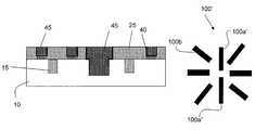
- FIG. 5shows additional processing steps and a respective structure, in accordance with aspects of the present invention.
- the backside of the substrate (wafer) 10undergoes a grinding or other removal process to expose the material 45 within the via 35 (now formed as a TSV 47 ).
- a metallization 50is formed on the backside of the substrate 10 , in contact with the TSV 47 .
- the dieis attached to a substrate 55 using a conductive adhesive, that forms an electrical connection to the metallization 50 .
- additional structures, devices, and/or metallization layerscan be formed over dielectric layer 25 , generally shown at reference numeral 60 .
- a wire 65can be connected between the substrate 55 and a device/structure 60 .
- FIGS. 6 a and 6 bshow alternative TSV structures fabricated in accordance with aspects of the present invention.
- the TSV structurescomprise a star configuration.
- the star configuration shown in FIGS. 6 a and 6 bare illustrative examples of such configuration, and that this should not be considered a limiting feature of the present invention.
- the TSV structurescan include more or less legs than shown in FIGS. 6 a and 6 b without departing from the scope of the present invention.
- the embodiments shown in FIGS. 6 a and 6 bcan be used in combination with the embodiments shown, for example, in FIGS. 1-5 .
- the TSV structures shown in FIGS. 6 a and 6 bcan be fabricated using conventional lithography, etching and deposition techniques.
- the TSV structures of both FIGS. 6 a and 6 bcan be lined with any appropriate liner material described herein, or can be devoid of a liner.
- the linercan be formed by a conventional CVD process.
- the TSV structures shown in FIGS. 6 a and 6 bcan be filled with any appropriate metal or metal alloy.
- the TSV structurescan be formed from any appropriately used refractory metal, e.g., tungsten, or copper, etc.
- the TSV structure 100comprises a single leg 100 a with six legs 100 b surrounding the leg 100 a , to form a star configuration.
- a minimum spacing between each of the legs 100 a , 100 bcan be about 5 microns; although the present invention contemplates a spacing from about 2 microns to about 10 microns. In embodiments, a spacing larger than 10 microns is also contemplated, but with the understanding that such spacing will require additional chip space. In further embodiments, the spacing can also be a function of the fill material, as understood by one of ordinary skill in the art.
- each of the legs 100 a , 100 bcan range from about 1 micron to about 10 microns, with a preference of about 3 microns. It should be understood that each leg of the same length should preferably have the same width due to etch stop considerations, e.g., to ensure that the legs are all of the same or substantially the same depth. Accordingly, in the example shown in FIG. 6 a , the leg 100 a may be slightly smaller in width than the remaining legs 100 b due to its larger length, to ensure that the etch depth remains the same for each leg 100 a , 100 b .
- the single leg 100 a(longer leg) may have a width of 2.8 microns; whereas, the other, shorter, legs 100 b may have a width of about 3 microns. In this way, all of the legs 100 a , 100 b would have the same etch depth.
- FIG. 6 bshows a variation of the TSV structure of FIG. 6 a .
- the single legis broken into two legs 100 a ′ and 100 a ′′.
- the TSV structure 100 ′also includes the six legs 100 b surrounding the legs 100 a ′ and 100 a ′′, to form the star configuration.
- the two legs 100 a ′ and 100 a ′′can be substantially of the same length and width as the legs 100 b . Accordingly, in this configuration, the etch depth will also be the same or substantially the same.
- FIG. 1shows a variation of the TSV structure of FIG. 6 a .
- the single legis broken into two legs 100 a ′ and 100 a ′′.
- the TSV structure 100 ′also includes the six legs 100 b surrounding the legs 100 a ′ and 100 a ′′, to form the star configuration.
- the two legs 100 a ′ and 100 a ′′can be substantially of the same length and width as the legs 100 b . Accordingly,
- the minimum spacing between each of the legs 100 a ′, 100 a ′′ and 100 bcan be about 5 microns; although a spacing of about 2 microns to about 10 microns (and greater) is also contemplated by the present invention.
- the width of each of the legs 100 a ′, 100 a ′′ and 100 bcan range from about 1 micron to about 10 microns, with a preference of about 3 microns.
- the legs 100 a ′, 100 a ′′ and 100 bmay each have a width of about 3 microns.
- FIG. 7shows a graph comparing fracture strength of a TSV star configuration and other patterned structures.
- the left-side y-axisis representative of strength (MPa)
- the right-side y-axisis representative of area ( ⁇ 2 )
- the x-axisis representative of different TSV patterns.
- the different patternsinclude: annulus, star, 16 circles, 5 shortbar, basket weave, 2 bar wide, 5 squiggle, 2 bar narrow, 5 bar 4, 5 bar 2, 5 bar 3 and a grid pattern, as would be known by those of skill in the art.
- the diamondsare representative of metal fill area
- the circlesare representative of a TiN lined TSV
- the squaresare representative of a TiW lined TSV.
- the star configuration of the present inventionprovides a significantly improved fracture strength for both a TiN liner and TiW liner, while also providing less metal area.
- the relatively high metal areaimportantly results in a relatively low resistance and inductance. Accordingly, it is possible to maximize fracture strength while providing the highest metal area that is possible (i.e., for low inductance and low resistance).
- the star designhas the highest metal area for designs that result in high fracture strength.
- FIG. 8is a flow diagram of a design process used in semiconductor design, manufacture, and/or test.
- FIG. 8shows a block diagram of an exemplary design flow 900 used for example, in semiconductor IC logic design, simulation, test, layout, and manufacture.
- Design flow 900includes processes, machines and/or mechanisms for processing design structures or devices to generate logically or otherwise functionally equivalent representations of the design structures and/or devices described above and shown in FIGS. 2-5 , 6 a and 6 b .
- the design structures processed and/or generated by design flow 900may be encoded on machine-readable transmission or storage media to include data and/or instructions that when executed or otherwise processed on a data processing system generate a logically, structurally, mechanically, or otherwise functionally equivalent representation of hardware components, circuits, devices, or systems.
- Machinesinclude, but are not limited to, any machine used in an IC design process, such as designing, manufacturing, or simulating a circuit, component, device, or system.
- machinesmay include: lithography machines, machines and/or equipment for generating masks (e.g. e-beam writers), computers or equipment for simulating design structures, any apparatus used in the manufacturing or test process, or any machines for programming functionally equivalent representations of the design structures into any medium (e.g. a machine for programming a programmable gate array).
- Design flow 900may vary depending on the type of representation being designed. For example, a design flow 900 for building an application specific IC (ASIC) may differ from a design flow 900 for designing a standard component or from a design flow 900 for instantiating the design into a programmable array, for example a programmable gate array (PGA) or a field programmable gate array (FPGA) offered by Altera® Inc. or Xilinx® Inc.
- ASICapplication specific IC
- PGAprogrammable gate array
- FPGAfield programmable gate array
- FIG. 8illustrates multiple such design structures including an input design structure 920 that is preferably processed by a design process 910 .
- Design structure 920may be a logical simulation design structure generated and processed by design process 910 to produce a logically equivalent functional representation of a hardware device.
- Design structure 920may also or alternatively comprise data and/or program instructions that when processed by design process 910 , generate a functional representation of the physical structure of a hardware device. Whether representing functional and/or structural design features, design structure 920 may be generated using electronic computer-aided design (ECAD) such as implemented by a core developer/designer.
- ECADelectronic computer-aided design
- design structure 920When encoded on a machine-readable data transmission, gate array, or storage medium, design structure 920 may be accessed and processed by one or more hardware and/or software modules within design process 910 to simulate or otherwise functionally represent an electronic component, circuit, electronic or logic module, apparatus, device, or system such as those shown in FIGS. 2-5 , 6 a and 6 b .
- design structure 920may comprise files or other data structures including human and/or machine-readable source code, compiled structures, and computer-executable code structures that when processed by a design or simulation data processing system, functionally simulate or otherwise represent circuits or other levels of hardware logic design.
- Such data structuresmay include hardware-description language (HDL) design entities or other data structures conforming to and/or compatible with lower-level HDL design languages such as Verilog and VHDL, and/or higher level design languages such as C or C++.
- HDLhardware-description language
- Design process 910preferably employs and incorporates hardware and/or software modules for synthesizing, translating, or otherwise processing a design/simulation functional equivalent of the components, circuits, devices, or logic structures shown in FIGS. 2-5 , 6 a and 6 b and to generate a netlist 980 which may contain design structures such as design structure 920 .
- Netlist 980may comprise, for example, compiled or otherwise processed data structures representing a list of wires, discrete components, logic gates, control circuits, I/O devices, models, etc. that describes the connections to other elements and circuits in an integrated circuit design.
- Netlist 980may be synthesized using an iterative process in which netlist 980 is resynthesized one or more times depending on design specifications and parameters for the device.
- netlist 980may be recorded on a machine-readable data storage medium or programmed into a programmable gate array.
- the mediummay be a non-volatile storage medium such as a magnetic or optical disk drive, a programmable gate array, a compact flash, or other flash memory. Additionally, or in the alternative, the medium may be a system or cache memory, buffer space, or electrically or optically conductive devices and materials on which data packets may be transmitted and intermediately stored via the Internet, or other networking suitable means.
- Design process 910may include hardware and software modules for processing a variety of input data structure types including netlist 980 .
- data structure typesmay reside, for example, within library elements 930 and include a set of commonly used elements, circuits, and devices, including models, layouts, and symbolic representations, for a given manufacturing technology (e.g., different technology nodes, 32 nm, 45 nm, 90 nm, etc.).
- the data structure typesmay further include design specifications 940 , characterization data 950 , verification data 960 , design rules 970 , and test data files 985 which may include input test patterns, output test results, and other testing information.
- Design process 910may further include, for example, standard mechanical design processes such as stress analysis, thermal analysis, mechanical event simulation, process simulation for operations such as casting, molding, and die press forming, etc.
- standard mechanical design processessuch as stress analysis, thermal analysis, mechanical event simulation, process simulation for operations such as casting, molding, and die press forming, etc.
- One of ordinary skill in the art of mechanical designcan appreciate the extent of possible mechanical design tools and applications used in design process 910 without deviating from the scope and spirit of the invention.
- Design process 910may also include modules for performing standard circuit design processes such as timing analysis, verification, design rule checking, place and route operations, etc.
- Design process 910employs and incorporates logic and physical design tools such as HDL compilers and simulation model build tools to process design structure 920 together with some or all of the depicted supporting data structures along with any additional mechanical design or data (if applicable), to generate a second design structure 990 .
- logic and physical design toolssuch as HDL compilers and simulation model build tools
- Design structure 990resides on a storage medium or programmable gate array in a data format used for the exchange of data of mechanical devices and structures (e.g. information stored in a IGES, DXF, Parasolid XT, JT, DRG, or any other suitable format for storing or rendering such mechanical design structures). Similar to design structure 920 , design structure 990 preferably comprises one or more files, data structures, or other computer-encoded data or instructions that reside on transmission or data storage media and that when processed by an ECAD system generate a logically or otherwise functionally equivalent form of one or more of the embodiments of the invention shown in FIGS. 2-5 , 6 a and 6 b . In one embodiment, design structure 990 may comprise a compiled, executable HDL simulation model that functionally simulates the devices shown in FIGS. 2-5 , 6 a and 6 b.
- a compiled, executable HDL simulation modelthat functionally simulates the devices shown in FIGS. 2-5 , 6 a and 6 b.
- Design structure 990may also employ a data format used for the exchange of layout data of integrated circuits and/or symbolic data format (e.g. information stored in a GDSII (GDS2), GL1, OASIS, map files, or any other suitable format for storing such design data structures).
- Design structure 990may comprise information such as, for example, symbolic data, map files, test data files, design content files, manufacturing data, layout parameters, wires, levels of metal, vias, shapes, data for routing through the manufacturing line, and any other data required by a manufacturer or other designer/developer to produce a device or structure as described above and shown in FIGS. 2-5 , 6 a and 6 b .
- Design structure 990may then proceed to a stage 995 where, for example, design structure 990 : proceeds to tape-out, is released to manufacturing, is released to a mask house, is sent to another design house, is sent back to the customer, etc.
- the method as described aboveis used in the fabrication of integrated circuit chips.
- the resulting integrated circuit chipscan be distributed by the fabricator in raw wafer form (that is, as a single wafer that has multiple unpackaged chips), as a bare die, or in a packaged form.
- the chipis mounted in a single chip package (such as a plastic carrier, with leads that are affixed to a motherboard or other higher level carrier) or in a multichip package (such as a ceramic carrier that has either or both surface interconnections or buried interconnections).
- the chipis then integrated with other chips, discrete circuit elements, and/or other signal processing devices as part of either (a) an intermediate product, such as a motherboard, or (b) an end product.
- the end productcan be any product that includes integrated circuit chips, ranging from toys and other low-end applications to advanced computer products having a display, a keyboard or other input device, and a central processor.
Landscapes
- Engineering & Computer Science (AREA)
- Computer Hardware Design (AREA)
- Physics & Mathematics (AREA)
- General Physics & Mathematics (AREA)
- Microelectronics & Electronic Packaging (AREA)
- Condensed Matter Physics & Semiconductors (AREA)
- Power Engineering (AREA)
- Theoretical Computer Science (AREA)
- Manufacturing & Machinery (AREA)
- General Engineering & Computer Science (AREA)
- Geometry (AREA)
- Evolutionary Computation (AREA)
- Computer Networks & Wireless Communication (AREA)
- Internal Circuitry In Semiconductor Integrated Circuit Devices (AREA)
Abstract
Description
Claims (20)
Priority Applications (3)
| Application Number | Priority Date | Filing Date | Title |
|---|---|---|---|
| US13/626,025US8791016B2 (en) | 2012-09-25 | 2012-09-25 | Through silicon via wafer, contacts and design structures |
| CN201310447344.2ACN103681474B (en) | 2012-09-25 | 2013-09-25 | Semiconductor structure and its manufacture method, hardware description language design structure |
| US14/301,395US9245850B2 (en) | 2012-09-25 | 2014-06-11 | Through silicon via wafer, contacts and design structures |
Applications Claiming Priority (1)
| Application Number | Priority Date | Filing Date | Title |
|---|---|---|---|
| US13/626,025US8791016B2 (en) | 2012-09-25 | 2012-09-25 | Through silicon via wafer, contacts and design structures |
Related Child Applications (1)
| Application Number | Title | Priority Date | Filing Date |
|---|---|---|---|
| US14/301,395DivisionUS9245850B2 (en) | 2012-09-25 | 2014-06-11 | Through silicon via wafer, contacts and design structures |
Publications (2)
| Publication Number | Publication Date |
|---|---|
| US20140087557A1 US20140087557A1 (en) | 2014-03-27 |
| US8791016B2true US8791016B2 (en) | 2014-07-29 |
Family
ID=50318613
Family Applications (2)
| Application Number | Title | Priority Date | Filing Date |
|---|---|---|---|
| US13/626,025ActiveUS8791016B2 (en) | 2012-09-25 | 2012-09-25 | Through silicon via wafer, contacts and design structures |
| US14/301,395ActiveUS9245850B2 (en) | 2012-09-25 | 2014-06-11 | Through silicon via wafer, contacts and design structures |
Family Applications After (1)
| Application Number | Title | Priority Date | Filing Date |
|---|---|---|---|
| US14/301,395ActiveUS9245850B2 (en) | 2012-09-25 | 2014-06-11 | Through silicon via wafer, contacts and design structures |
Country Status (2)
| Country | Link |
|---|---|
| US (2) | US8791016B2 (en) |
| CN (1) | CN103681474B (en) |
Cited By (6)
| Publication number | Priority date | Publication date | Assignee | Title |
|---|---|---|---|---|
| US20160111398A1 (en)* | 2012-09-10 | 2016-04-21 | Taiwan Semiconductor Manufacturing Company, Ltd. | Semiconductor Device with Discrete Blocks |
| US9490167B2 (en) | 2012-10-11 | 2016-11-08 | Taiwan Semiconductor Manufactoring Company, Ltd. | Pop structures and methods of forming the same |
| US9613917B2 (en) | 2012-03-30 | 2017-04-04 | Taiwan Semiconductor Manufacturing Company, Ltd. | Package-on-package (PoP) device with integrated passive device in a via |
| US9679839B2 (en) | 2013-10-30 | 2017-06-13 | Taiwan Semiconductor Manufacturing Company, Ltd. | Chip on package structure and method |
| US9704826B2 (en) | 2013-10-30 | 2017-07-11 | Taiwan Semiconductor Manufacturing Company, Ltd. | Chip on package structure and method |
| US10109567B2 (en) | 2012-10-19 | 2018-10-23 | Taiwan Semiconductor Manufacturing Company, Ltd. | Fan-out wafer level package structure |
Families Citing this family (4)
| Publication number | Priority date | Publication date | Assignee | Title |
|---|---|---|---|---|
| CN103956334B (en)* | 2014-05-07 | 2016-06-01 | 华进半导体封装先导技术研发中心有限公司 | RDL and TSV metal level one-step moulding method in unicircuit |
| US9923011B2 (en)* | 2016-01-12 | 2018-03-20 | Taiwan Semiconductor Manufacturing Co., Ltd. | Semiconductor device structure with stacked semiconductor dies |
| US20190125075A1 (en)* | 2016-04-25 | 2019-05-02 | Corning Incorporated | Workstation comprising work surface comprising integrated display protected by strengthened glass laminate cover |
| CN111244219B (en)* | 2020-01-17 | 2021-10-26 | 南京大学 | Solar energy thermal photovoltaic cell based on silicon-based single-side integrated absorption emitter |
Citations (17)
| Publication number | Priority date | Publication date | Assignee | Title |
|---|---|---|---|---|
| US5219789A (en) | 1991-04-19 | 1993-06-15 | Sharp Kabushiki Kaisha | Method for forming contact portion of semiconductor device |
| US6270601B1 (en) | 1998-11-02 | 2001-08-07 | Coorstek, Inc. | Method for producing filled vias in electronic components |
| US6365513B1 (en)* | 1997-10-01 | 2002-04-02 | Matsushita Electric Industrial Co., Ltd. | Method of making a semiconductor device including testing before thinning the semiconductor substrate |
| US6887785B1 (en)* | 2004-05-13 | 2005-05-03 | International Business Machines Corporation | Etching openings of different depths using a single mask layer method and structure |
| US6976238B1 (en) | 2001-06-03 | 2005-12-13 | Cadence Design Systems, Inc. | Circular vias and interconnect-line ends |
| US7060624B2 (en) | 2003-08-13 | 2006-06-13 | International Business Machines Corporation | Deep filled vias |
| US7521360B2 (en) | 2003-04-09 | 2009-04-21 | Tru-Si Technologies, Inc. | Electroplating and electroless plating of conductive materials into openings, and structures obtained thereby |
| US20100009531A1 (en)* | 2008-07-10 | 2010-01-14 | Samsung Electronics Co., Ltd. | Methods of forming a contact structure |
| US7741226B2 (en) | 2008-05-06 | 2010-06-22 | International Business Machines Corporation | Optimal tungsten through wafer via and process of fabricating same |
| US20100187670A1 (en)* | 2009-01-26 | 2010-07-29 | Chuan-Yi Lin | On-Chip Heat Spreader |
| US7830018B2 (en) | 2007-08-31 | 2010-11-09 | Micron Technology, Inc. | Partitioned through-layer via and associated systems and methods |
| US20110244676A1 (en)* | 2010-03-30 | 2011-10-06 | Taiwan Semiconductor Manufacturing Company, Ltd. | Chemical mechanical polishing (cmp) processing of through-silicon via (tsv) and contact plug simultaneously |
| US20110284992A1 (en) | 2010-05-24 | 2011-11-24 | Institute of Microelectronics, Chinese Academy of Sciences | 3d integrated circuit and method of manufacturing the same |
| US8080881B2 (en) | 2009-01-12 | 2011-12-20 | Vanguard International Semiconductor Corporation | Contact pad supporting structure and integrated circuit for crack suppresion |
| US8097955B2 (en) | 2008-10-15 | 2012-01-17 | Qimonda Ag | Interconnect structures and methods |
| US20120068356A1 (en) | 2010-09-21 | 2012-03-22 | Marcus Ahles | Component having a VIA |
| US20120074584A1 (en)* | 2010-09-27 | 2012-03-29 | Samsung Electronics Co., Ltd. | Multi-layer tsv insulation and methods of fabricating the same |
Family Cites Families (3)
| Publication number | Priority date | Publication date | Assignee | Title |
|---|---|---|---|---|
| US6388208B1 (en)* | 1999-06-11 | 2002-05-14 | Teradyne, Inc. | Multi-connection via with electrically isolated segments |
| US8214660B2 (en)* | 2006-07-26 | 2012-07-03 | International Business Machines Corporation | Structure for an apparatus for monitoring and controlling heat generation in a multi-core processor |
| US7968975B2 (en)* | 2008-08-08 | 2011-06-28 | International Business Machines Corporation | Metal wiring structure for integration with through substrate vias |
- 2012
- 2012-09-25USUS13/626,025patent/US8791016B2/enactiveActive
- 2013
- 2013-09-25CNCN201310447344.2Apatent/CN103681474B/enactiveActive
- 2014
- 2014-06-11USUS14/301,395patent/US9245850B2/enactiveActive
Patent Citations (17)
| Publication number | Priority date | Publication date | Assignee | Title |
|---|---|---|---|---|
| US5219789A (en) | 1991-04-19 | 1993-06-15 | Sharp Kabushiki Kaisha | Method for forming contact portion of semiconductor device |
| US6365513B1 (en)* | 1997-10-01 | 2002-04-02 | Matsushita Electric Industrial Co., Ltd. | Method of making a semiconductor device including testing before thinning the semiconductor substrate |
| US6270601B1 (en) | 1998-11-02 | 2001-08-07 | Coorstek, Inc. | Method for producing filled vias in electronic components |
| US6976238B1 (en) | 2001-06-03 | 2005-12-13 | Cadence Design Systems, Inc. | Circular vias and interconnect-line ends |
| US7521360B2 (en) | 2003-04-09 | 2009-04-21 | Tru-Si Technologies, Inc. | Electroplating and electroless plating of conductive materials into openings, and structures obtained thereby |
| US7060624B2 (en) | 2003-08-13 | 2006-06-13 | International Business Machines Corporation | Deep filled vias |
| US6887785B1 (en)* | 2004-05-13 | 2005-05-03 | International Business Machines Corporation | Etching openings of different depths using a single mask layer method and structure |
| US7830018B2 (en) | 2007-08-31 | 2010-11-09 | Micron Technology, Inc. | Partitioned through-layer via and associated systems and methods |
| US7741226B2 (en) | 2008-05-06 | 2010-06-22 | International Business Machines Corporation | Optimal tungsten through wafer via and process of fabricating same |
| US20100009531A1 (en)* | 2008-07-10 | 2010-01-14 | Samsung Electronics Co., Ltd. | Methods of forming a contact structure |
| US8097955B2 (en) | 2008-10-15 | 2012-01-17 | Qimonda Ag | Interconnect structures and methods |
| US8080881B2 (en) | 2009-01-12 | 2011-12-20 | Vanguard International Semiconductor Corporation | Contact pad supporting structure and integrated circuit for crack suppresion |
| US20100187670A1 (en)* | 2009-01-26 | 2010-07-29 | Chuan-Yi Lin | On-Chip Heat Spreader |
| US20110244676A1 (en)* | 2010-03-30 | 2011-10-06 | Taiwan Semiconductor Manufacturing Company, Ltd. | Chemical mechanical polishing (cmp) processing of through-silicon via (tsv) and contact plug simultaneously |
| US20110284992A1 (en) | 2010-05-24 | 2011-11-24 | Institute of Microelectronics, Chinese Academy of Sciences | 3d integrated circuit and method of manufacturing the same |
| US20120068356A1 (en) | 2010-09-21 | 2012-03-22 | Marcus Ahles | Component having a VIA |
| US20120074584A1 (en)* | 2010-09-27 | 2012-03-29 | Samsung Electronics Co., Ltd. | Multi-layer tsv insulation and methods of fabricating the same |
Non-Patent Citations (4)
| Title |
|---|
| Dudek et al. "Thermo-Mechanical Reliability Assessment for 3D Through-Si Stacking", 2009 IEEE, 10th Int. Conf. on Thermal, Mechanical and Multiphysics Simulation and Experiments in Micro-Electronics and Micro-Systems, EuroSimE 2009, 7 pages. |
| Malladi et al. "3D Integration Techniques Applied to SiGe Power Amplifiers", IBM Semiconductor Research and Development Center, Essex Junction, http://www.ecsdl.org/terms-use.jsp, The Electrochemical Society, pp. 1053-1067, 2008. |
| Stamper et al. "CMOS Compatible Insulated Through Silicon Vias for 3D Silicon", Advanced Metallization Conference, 2009, IBM Microelectronics, 8 pages. |
| Stamper et al. "Through Wafer Via Integration in CMOS and BiCMOS Technologies", Advanced Metallization Conference, 2008, IBM Microelectronics, 6 pages.* |
Cited By (20)
| Publication number | Priority date | Publication date | Assignee | Title |
|---|---|---|---|---|
| US10163873B2 (en) | 2012-03-30 | 2018-12-25 | Taiwan Semiconductor Manufacturing Company | Package-on-package (PoP) device with integrated passive device in a via |
| US10978433B2 (en) | 2012-03-30 | 2021-04-13 | Taiwan Semiconductor Manufacturing Company | Package-on-package (PoP) device with integrated passive device in a via |
| US10515938B2 (en) | 2012-03-30 | 2019-12-24 | Taiwan Semiconductor Manufacturing Company | Package on-package (PoP) device with integrated passive device in a via |
| US9613917B2 (en) | 2012-03-30 | 2017-04-04 | Taiwan Semiconductor Manufacturing Company, Ltd. | Package-on-package (PoP) device with integrated passive device in a via |
| US11217562B2 (en) | 2012-09-10 | 2022-01-04 | Taiwan Semiconductor Manufacturing Company, Ltd. | Semiconductor device with discrete blocks |
| US9543278B2 (en)* | 2012-09-10 | 2017-01-10 | Taiwan Semiconductor Manufacturing Company, Ltd. | Semiconductor device with discrete blocks |
| US10008479B2 (en) | 2012-09-10 | 2018-06-26 | Taiwan Semiconductor Manufacturing Company, Ltd. | Semiconductor device with discrete blocks |
| US12334476B2 (en) | 2012-09-10 | 2025-06-17 | Taiwan Semiconductor Manufacturing Company, Ltd. | Semiconductor device with discrete blocks |
| US11855045B2 (en) | 2012-09-10 | 2023-12-26 | Taiwan Semiconductor Manufacturing Company, Ltd. | Semiconductor device with discrete blocks |
| US20160111398A1 (en)* | 2012-09-10 | 2016-04-21 | Taiwan Semiconductor Manufacturing Company, Ltd. | Semiconductor Device with Discrete Blocks |
| US10510727B2 (en) | 2012-09-10 | 2019-12-17 | Taiwan Semiconductor Manufacturing Company, Ltd. | Semiconductor device with discrete blocks |
| US9490167B2 (en) | 2012-10-11 | 2016-11-08 | Taiwan Semiconductor Manufactoring Company, Ltd. | Pop structures and methods of forming the same |
| US10804187B2 (en) | 2012-10-19 | 2020-10-13 | Taiwan Semiconductor Manufacturing Company, Ltd. | Fan-out wafer level package structure |
| US11527464B2 (en) | 2012-10-19 | 2022-12-13 | Taiwan Semiconductor Manufacturing Company, Ltd. | Fan-out wafer level package structure |
| US12170242B2 (en) | 2012-10-19 | 2024-12-17 | Taiwan Semiconductor Manufacturing Company, Ltd. | Fan-out wafer level package structure |
| US10109567B2 (en) | 2012-10-19 | 2018-10-23 | Taiwan Semiconductor Manufacturing Company, Ltd. | Fan-out wafer level package structure |
| US10964666B2 (en) | 2013-10-30 | 2021-03-30 | Taiwan Semiconductor Manufacturing Company, Ltd. | Chip on package structure and method |
| US9704826B2 (en) | 2013-10-30 | 2017-07-11 | Taiwan Semiconductor Manufacturing Company, Ltd. | Chip on package structure and method |
| US10510717B2 (en) | 2013-10-30 | 2019-12-17 | Taiwan Semiconductor Manufacturing Company, Ltd. | Chip on package structure and method |
| US9679839B2 (en) | 2013-10-30 | 2017-06-13 | Taiwan Semiconductor Manufacturing Company, Ltd. | Chip on package structure and method |
Also Published As
| Publication number | Publication date |
|---|---|
| US9245850B2 (en) | 2016-01-26 |
| CN103681474B (en) | 2017-03-01 |
| US20140087557A1 (en) | 2014-03-27 |
| CN103681474A (en) | 2014-03-26 |
| US20140284816A1 (en) | 2014-09-25 |
Similar Documents
| Publication | Publication Date | Title |
|---|---|---|
| US8791016B2 (en) | Through silicon via wafer, contacts and design structures | |
| EP1783834B1 (en) | Support structure for semiconductor device bond pads and method of making the same | |
| US9911682B2 (en) | Phase changing on-chip thermal heat sink | |
| US20150145144A1 (en) | Use of a conformal coating elastic cushion to reduce through silicon vias (tsv) stress in 3-dimensional integration | |
| US8877559B2 (en) | Through-silicon via with sidewall air gap | |
| US9455214B2 (en) | Wafer frontside-backside through silicon via | |
| WO2010017062A1 (en) | Metal wiring structure for integration with through substrate vias | |
| JP2015502074A (en) | Manufacturing method, structure, and design structure of integrated semiconductor device with amorphous silicon beam | |
| JP2008085226A (en) | Semiconductor wafer, its manufacturing method, and method of manufacturing semiconductor device | |
| US8987067B2 (en) | Segmented guard ring structures with electrically insulated gap structures and design structures thereof | |
| US20130270678A1 (en) | Integrated circuit including thermal gate, related method and design structure | |
| US8645898B2 (en) | Structure and design structure for high-Q value inductor and method of manufacturing the same | |
| US20160284645A1 (en) | Semiconductor structures having low resistance paths throughout a wafer | |
| WO2019118122A1 (en) | Selective recess | |
| US20160035668A1 (en) | Automated short lenght wire shape strapping and methods of fabricating the same | |
| US20150221631A1 (en) | Integrated passive devices for finfet technologies | |
| US9231046B2 (en) | Capacitor using barrier layer metallurgy | |
| US9041210B2 (en) | Through silicon via wafer and methods of manufacturing | |
| CN108231737A (en) | For reducing the silicon hole with improvement substrate contact of silicon hole capacitance variation | |
| US9059111B2 (en) | Reliable back-side-metal structure | |
| US8912091B2 (en) | Backside metal ground plane with improved metal adhesion and design structures | |
| CN103579088B (en) | A kind of preparation method of semiconductor device silicon through hole | |
| CN113644025A (en) | Through hole filling method and through hole |
Legal Events
| Date | Code | Title | Description |
|---|---|---|---|
| AS | Assignment | Owner name:INTERNATIONAL BUSINESS MACHINES CORPORATION, NEW Y Free format text:ASSIGNMENT OF ASSIGNORS INTEREST;ASSIGNORS:GAMBINO, JEFFREY P.;LUCE, CAMERON E.;VANSLETTE, DANIEL S.;AND OTHERS;SIGNING DATES FROM 20120918 TO 20120920;REEL/FRAME:029019/0944 | |
| STCF | Information on status: patent grant | Free format text:PATENTED CASE | |
| AS | Assignment | Owner name:GLOBALFOUNDRIES U.S. 2 LLC, NEW YORK Free format text:ASSIGNMENT OF ASSIGNORS INTEREST;ASSIGNOR:INTERNATIONAL BUSINESS MACHINES CORPORATION;REEL/FRAME:036550/0001 Effective date:20150629 | |
| AS | Assignment | Owner name:GLOBALFOUNDRIES INC., CAYMAN ISLANDS Free format text:ASSIGNMENT OF ASSIGNORS INTEREST;ASSIGNORS:GLOBALFOUNDRIES U.S. 2 LLC;GLOBALFOUNDRIES U.S. INC.;REEL/FRAME:036779/0001 Effective date:20150910 | |
| MAFP | Maintenance fee payment | Free format text:PAYMENT OF MAINTENANCE FEE, 4TH YEAR, LARGE ENTITY (ORIGINAL EVENT CODE: M1551) Year of fee payment:4 | |
| AS | Assignment | Owner name:WILMINGTON TRUST, NATIONAL ASSOCIATION, DELAWARE Free format text:SECURITY AGREEMENT;ASSIGNOR:GLOBALFOUNDRIES INC.;REEL/FRAME:049490/0001 Effective date:20181127 | |
| AS | Assignment | Owner name:GLOBALFOUNDRIES U.S. INC., CALIFORNIA Free format text:ASSIGNMENT OF ASSIGNORS INTEREST;ASSIGNOR:GLOBALFOUNDRIES INC.;REEL/FRAME:054633/0001 Effective date:20201022 | |
| AS | Assignment | Owner name:GLOBALFOUNDRIES INC., CAYMAN ISLANDS Free format text:RELEASE BY SECURED PARTY;ASSIGNOR:WILMINGTON TRUST, NATIONAL ASSOCIATION;REEL/FRAME:054636/0001 Effective date:20201117 | |
| AS | Assignment | Owner name:GLOBALFOUNDRIES U.S. INC., NEW YORK Free format text:RELEASE BY SECURED PARTY;ASSIGNOR:WILMINGTON TRUST, NATIONAL ASSOCIATION;REEL/FRAME:056987/0001 Effective date:20201117 | |
| MAFP | Maintenance fee payment | Free format text:PAYMENT OF MAINTENANCE FEE, 8TH YEAR, LARGE ENTITY (ORIGINAL EVENT CODE: M1552); ENTITY STATUS OF PATENT OWNER: LARGE ENTITY Year of fee payment:8 |