US8791010B1 - Silver interconnects for stacked non-volatile memory device and method - Google Patents
Silver interconnects for stacked non-volatile memory device and methodDownload PDFInfo
- Publication number
- US8791010B1 US8791010B1US13/339,851US201113339851AUS8791010B1US 8791010 B1US8791010 B1US 8791010B1US 201113339851 AUS201113339851 AUS 201113339851AUS 8791010 B1US8791010 B1US 8791010B1
- Authority
- US
- United States
- Prior art keywords
- overlying
- dielectric
- wiring structure
- silver
- switching
- Prior art date
- Legal status (The legal status is an assumption and is not a legal conclusion. Google has not performed a legal analysis and makes no representation as to the accuracy of the status listed.)
- Expired - Fee Related, expires
Links
- 238000000034methodMethods0.000titleclaimsabstractdescription83
- BQCADISMDOOEFD-UHFFFAOYSA-NSilverChemical compound[Ag]BQCADISMDOOEFD-UHFFFAOYSA-N0.000titleclaimsabstractdescription62
- 229910052709silverInorganic materials0.000titleclaimsabstractdescription62
- 239000004332silverSubstances0.000titleclaimsabstractdescription62
- 239000000463materialSubstances0.000claimsabstractdescription161
- 239000003989dielectric materialSubstances0.000claimsabstractdescription66
- 239000000758substrateSubstances0.000claimsabstractdescription32
- 229910021417amorphous siliconInorganic materials0.000claimsabstractdescription29
- 230000015654memoryEffects0.000claimsdescription51
- 230000008569processEffects0.000claimsdescription31
- 239000004065semiconductorSubstances0.000claimsdescription18
- 238000000151depositionMethods0.000claimsdescription15
- 239000002210silicon-based materialSubstances0.000claimsdescription14
- VYPSYNLAJGMNEJ-UHFFFAOYSA-NSilicium dioxideChemical compoundO=[Si]=OVYPSYNLAJGMNEJ-UHFFFAOYSA-N0.000claimsdescription11
- 238000000059patterningMethods0.000claimsdescription11
- 229910052814silicon oxideInorganic materials0.000claimsdescription11
- 229910021420polycrystalline siliconInorganic materials0.000claimsdescription10
- 229920005591polysiliconPolymers0.000claimsdescription10
- 238000005530etchingMethods0.000claimsdescription9
- 229910052581Si3N4Inorganic materials0.000claimsdescription8
- HQVNEWCFYHHQES-UHFFFAOYSA-Nsilicon nitrideChemical compoundN12[Si]34N5[Si]62N3[Si]51N64HQVNEWCFYHHQES-UHFFFAOYSA-N0.000claimsdescription8
- XUIMIQQOPSSXEZ-UHFFFAOYSA-NSiliconChemical compound[Si]XUIMIQQOPSSXEZ-UHFFFAOYSA-N0.000claimsdescription7
- 229910052710siliconInorganic materials0.000claimsdescription7
- 239000010703siliconSubstances0.000claimsdescription7
- NRTOMJZYCJJWKI-UHFFFAOYSA-NTitanium nitrideChemical compound[Ti]#NNRTOMJZYCJJWKI-UHFFFAOYSA-N0.000claimsdescription5
- 230000004888barrier functionEffects0.000claimsdescription5
- 238000005240physical vapour depositionMethods0.000claimsdescription5
- 125000006850spacer groupChemical group0.000claimsdescription5
- 229910052721tungstenInorganic materials0.000claimsdescription5
- 239000010937tungstenSubstances0.000claimsdescription5
- 229910000577Silicon-germaniumInorganic materials0.000claimsdescription4
- RTAQQCXQSZGOHL-UHFFFAOYSA-NTitaniumChemical compound[Ti]RTAQQCXQSZGOHL-UHFFFAOYSA-N0.000claimsdescription4
- LEVVHYCKPQWKOP-UHFFFAOYSA-N[Si].[Ge]Chemical compound[Si].[Ge]LEVVHYCKPQWKOP-UHFFFAOYSA-N0.000claimsdescription4
- 239000012212insulatorSubstances0.000claimsdescription4
- 229910021421monocrystalline siliconInorganic materials0.000claimsdescription4
- MZLGASXMSKOWSE-UHFFFAOYSA-Ntantalum nitrideChemical compound[Ta]#NMZLGASXMSKOWSE-UHFFFAOYSA-N0.000claimsdescription4
- 239000010936titaniumSubstances0.000claimsdescription4
- 229910052719titaniumInorganic materials0.000claimsdescription4
- -1tungsten nitrideChemical class0.000claimsdescription4
- 230000008021depositionEffects0.000claimsdescription3
- 238000009792diffusion processMethods0.000claimsdescription3
- 238000009713electroplatingMethods0.000claimsdescription3
- 230000007547defectEffects0.000claimsdescription2
- HBMJWWWQQXIZIP-UHFFFAOYSA-Nsilicon carbideChemical compound[Si+]#[C-]HBMJWWWQQXIZIP-UHFFFAOYSA-N0.000claimsdescription2
- 229910010271silicon carbideInorganic materials0.000claimsdescription2
- 238000004070electrodepositionMethods0.000claims1
- 239000010410layerSubstances0.000description8
- 229910052751metalInorganic materials0.000description7
- 239000002184metalSubstances0.000description7
- 238000003491arrayMethods0.000description6
- 230000008901benefitEffects0.000description4
- 238000005229chemical vapour depositionMethods0.000description4
- 238000004519manufacturing processMethods0.000description4
- 238000012986modificationMethods0.000description4
- 230000004048modificationEffects0.000description4
- 150000002500ionsChemical class0.000description3
- 229920002120photoresistant polymerPolymers0.000description3
- XKRFYHLGVUSROY-UHFFFAOYSA-NArgonChemical compound[Ar]XKRFYHLGVUSROY-UHFFFAOYSA-N0.000description2
- 239000006117anti-reflective coatingSubstances0.000description2
- 238000005137deposition processMethods0.000description2
- 238000010586diagramMethods0.000description2
- ZOXJGFHDIHLPTG-UHFFFAOYSA-NBoronChemical compound[B]ZOXJGFHDIHLPTG-UHFFFAOYSA-N0.000description1
- RYGMFSIKBFXOCR-UHFFFAOYSA-NCopperChemical compound[Cu]RYGMFSIKBFXOCR-UHFFFAOYSA-N0.000description1
- PXGOKWXKJXAPGV-UHFFFAOYSA-NFluorineChemical compoundFFPXGOKWXKJXAPGV-UHFFFAOYSA-N0.000description1
- 229910052782aluminiumInorganic materials0.000description1
- XAGFODPZIPBFFR-UHFFFAOYSA-NaluminiumChemical compound[Al]XAGFODPZIPBFFR-UHFFFAOYSA-N0.000description1
- 229910052786argonInorganic materials0.000description1
- 230000006399behaviorEffects0.000description1
- 229910052796boronInorganic materials0.000description1
- 230000008859changeEffects0.000description1
- 229910052802copperInorganic materials0.000description1
- 239000010949copperSubstances0.000description1
- 230000000694effectsEffects0.000description1
- 230000005669field effectEffects0.000description1
- 229910052731fluorineInorganic materials0.000description1
- 239000011737fluorineSubstances0.000description1
- 239000011521glassSubstances0.000description1
- BHEPBYXIRTUNPN-UHFFFAOYSA-Nhydridophosphorus(.) (triplet)Chemical compound[PH]BHEPBYXIRTUNPN-UHFFFAOYSA-N0.000description1
- 239000012535impuritySubstances0.000description1
- 230000010354integrationEffects0.000description1
- 238000004518low pressure chemical vapour depositionMethods0.000description1
- 239000007769metal materialSubstances0.000description1
- 238000001465metallisationMethods0.000description1
- 239000002245particleSubstances0.000description1
- 230000002093peripheral effectEffects0.000description1
- 238000000623plasma-assisted chemical vapour depositionMethods0.000description1
- 238000007517polishing processMethods0.000description1
- 239000002356single layerSubstances0.000description1
- 239000000126substanceSubstances0.000description1
- WFKWXMTUELFFGS-UHFFFAOYSA-NtungstenChemical compound[W]WFKWXMTUELFFGS-UHFFFAOYSA-N0.000description1
Images


Classifications
- H—ELECTRICITY
- H10—SEMICONDUCTOR DEVICES; ELECTRIC SOLID-STATE DEVICES NOT OTHERWISE PROVIDED FOR
- H10B—ELECTRONIC MEMORY DEVICES
- H10B63/00—Resistance change memory devices, e.g. resistive RAM [ReRAM] devices
- H10B63/80—Arrangements comprising multiple bistable or multi-stable switching components of the same type on a plane parallel to the substrate, e.g. cross-point arrays
- H10B63/84—Arrangements comprising multiple bistable or multi-stable switching components of the same type on a plane parallel to the substrate, e.g. cross-point arrays arranged in a direction perpendicular to the substrate, e.g. 3D cell arrays
- H—ELECTRICITY
- H10—SEMICONDUCTOR DEVICES; ELECTRIC SOLID-STATE DEVICES NOT OTHERWISE PROVIDED FOR
- H10N—ELECTRIC SOLID-STATE DEVICES NOT OTHERWISE PROVIDED FOR
- H10N70/00—Solid-state devices having no potential barriers, and specially adapted for rectifying, amplifying, oscillating or switching
- H10N70/011—Manufacture or treatment of multistable switching devices
- H10N70/061—Shaping switching materials
- H10N70/063—Shaping switching materials by etching of pre-deposited switching material layers, e.g. lithography
- H—ELECTRICITY
- H10—SEMICONDUCTOR DEVICES; ELECTRIC SOLID-STATE DEVICES NOT OTHERWISE PROVIDED FOR
- H10N—ELECTRIC SOLID-STATE DEVICES NOT OTHERWISE PROVIDED FOR
- H10N70/00—Solid-state devices having no potential barriers, and specially adapted for rectifying, amplifying, oscillating or switching
- H10N70/20—Multistable switching devices, e.g. memristors
- H10N70/24—Multistable switching devices, e.g. memristors based on migration or redistribution of ionic species, e.g. anions, vacancies
- H10N70/245—Multistable switching devices, e.g. memristors based on migration or redistribution of ionic species, e.g. anions, vacancies the species being metal cations, e.g. programmable metallization cells
- H—ELECTRICITY
- H10—SEMICONDUCTOR DEVICES; ELECTRIC SOLID-STATE DEVICES NOT OTHERWISE PROVIDED FOR
- H10N—ELECTRIC SOLID-STATE DEVICES NOT OTHERWISE PROVIDED FOR
- H10N70/00—Solid-state devices having no potential barriers, and specially adapted for rectifying, amplifying, oscillating or switching
- H10N70/801—Constructional details of multistable switching devices
- H10N70/821—Device geometry
- H10N70/826—Device geometry adapted for essentially vertical current flow, e.g. sandwich or pillar type devices
- H—ELECTRICITY
- H10—SEMICONDUCTOR DEVICES; ELECTRIC SOLID-STATE DEVICES NOT OTHERWISE PROVIDED FOR
- H10N—ELECTRIC SOLID-STATE DEVICES NOT OTHERWISE PROVIDED FOR
- H10N70/00—Solid-state devices having no potential barriers, and specially adapted for rectifying, amplifying, oscillating or switching
- H10N70/801—Constructional details of multistable switching devices
- H10N70/881—Switching materials
- H10N70/884—Switching materials based on at least one element of group IIIA, IVA or VA, e.g. elemental or compound semiconductors
Definitions
- the present inventionis generally related to resistive switching devices. More particularly, embodiments according to the present invention provide a method and a structure for forming an interconnect structure for a stacked resistive switching device.
- the present inventioncan be applied to non-volatile memory devices but it should be recognized that the present invention can have a much broader range of applicability.
- FlashFlash memory is one type of non-volatile memory device.
- RAMnon-volatile random access memory
- Fe RAMferroelectric RAM
- MRAMmagneto-resistive RAM
- ORAMorganic RAM
- PCRAMphase change RAM
- Fe-RAM and MRAM deviceshave fast switching characteristics and good programming endurance, but their fabrication is not CMOS compatible and size is usually large. Switching a PCRAM device requires a large amount of power.
- Organic RAM or ORAMis incompatible with large volume silicon-based fabrication and device reliability is usually poor.
- the present inventionis generally related to resistive switching devices. More particularly, embodiments according to the present invention provide a method and a structure for forming an interconnect structure for a resistive switching device.
- the present inventioncan be applied to non-volatile memory devices but it should be recognized that the present invention can have a much broader range of applicability.
- a method of forming interconnects for a non-volatile memory deviceincludes providing a substrate having a surface region and forming a first thickness of dielectric material overlying the surface region.
- the methodincludes subjecting the first thickness of dielectric material to a first patterning and etching process to form a plurality of opening structures in a portion of the first dielectric material.
- a first lining materialis formed conformably overlying each of the plurality of opening structures.
- the methodincludes depositing a first silver material to fill each of the plurality of opening structures and forming a thickness of silver material overlying the first dielectric material.
- a second adhesion materialis formed overlying the thickness of silver material and a contact material is formed overlying the second adhesion material.
- the methodincludes depositing a switching material comprising an amorphous silicon material overlying the contact material.
- the switching material, the contact material, and the silver materialare subjected to a second patterning and etching process to form one or more first structures.
- Each of the one or more first structuresincludes at least a bottom wiring structure from at least the first silver material in a specific embodiment.
- the one or more bottom wiring structureis configured to spatially extend in a first direction in a specific embodiment.
- a thickness of second dielectric materialis deposited overlying the one or more first structures.
- the methodincludes subjecting the second dielectric material to a third patterning and etching process to form at least one via openings in a portion of the second dielectric material to expose a surface region of the switching material.
- the methodincludes depositing a second wiring material comprising a second silver material to fill the at least one via openings and to form a thickness of second wiring material overlying the second dielectric material.
- the second wiring materialis subjected to a fourth patterning and etching process to form a top wiring structure spatially extending in a second direction orthogonal to the first direction in a specific embodiment.
- a non-volatile memory device structurein a specific embodiment, includes a semiconductor substrate having a surface region and a first dielectric material overlying the surface region of the semiconductor substrate.
- the deviceincludes a bottom wiring structure comprising at least a first silver material overlying the first dielectric material.
- the bottom wiring structureis configured to spatially extend in a first direction.
- the deviceincludes a contact material comprising a p+ polysilicon material overlying the bottom wiring structure and a switching material comprising an amorphous silicon material overlying the contact material.
- a top wiring structurecomprising at least a second silver material overlies the switching material.
- the top wiring structureis configured to spatially extend in a second direction orthogonal to the first direction.
- a non-volatile memory devicein a specific embodiment, includes a semiconductor substrate having a surface region and a first dielectric material overlying the surface region of the semiconductor substrate.
- the non-volatile memory deviceincludes a first crossbar array of memory cells.
- the first crossbar array of memory cellsincludes a first bottom wiring structure comprising a first silver material spatially extending in a first direction, a first top wiring structure comprising a second silver material spatially extending in a second direction orthogonal to the first direction, and a first switching region comprising an amorphous silicon material sandwiched between the first wiring structure and the second wiring structure.
- a second dielectric materialoverlies the first crossbar array of memory cells.
- the non-volatile memory deviceincludes a second crossbar array of memory cells overlying the second dielectric material.
- the second crossbar array of memory cellsincludes at least a second bottom wiring structure comprising a third silver material spatially extending in the first direction, a second top wiring structure comprising a fourth silver material spatially extending in the second direction, and a second switching region sandwiched between the second bottom wiring structure and the second top wiring structure.
- the non-volatile memory devicecan have N crossbar arrays of memory cells, where N is an integer ranging from 1 to 8.
- an Nth crossbar array of memory cellsis isolated from an (N ⁇ 1)th crossbar array of memory cells by an Nth dielectric material.
- the present methoduses a silver material for interconnect structure to lower resistance in the circuitry of the non-volatile memory device to enhance device performance and decrease device size.
- silverwhich is also a material used in a memory cell, would greatly simplify process and increases device yield.
- a reduced thickness of an interconnect wiringcan be used due to the higher electric conductivity of silver.
- a reduced thickness in silverwould require less photoresist for pattern and etch.
- a thinner photoresistis required as device size shrinks.
- the methodprovides a way to form a multilayer vertically stacked non-volatile memory device characterized by high density and reduced feature size.
- FIGS. 1-7 , 7 ( a ), 8 , 8 ( a ), 9 , 9 ( a ), 10 , and 10 ( a )are simplified diagrams illustrating a method of forming a nonvolatile memory device according to embodiments of the present invention.
- FIG. 11is a simplified diagram illustrating a multilayer memory cell according to an embodiment of the present invention.
- the present inventionis directed to memory device. More particularly, embodiments according to the present invention provide a method and a structure for forming an interconnect structure for a memory device. Embodiments according to the present invention have been applied to a non-volatile memory device. But it should be recognized that the present invention can have a much broader range of applicability.
- a typical deviceconsists of a pair of metal electrodes sandwiching an amorphous-Si layer in a so-called Metal/a-Si/Metal (M/a-Si/M) structure, in which the voltage applied across the pair of metal electrodes causes changes in the a-Si resistance.
- M/a-Si/MMetal/a-Si/Metal
- These conventional M/a-Si/M based nonvolatile switching deviceshave the advantages of high Ion/Ioff ratios, and can be fabricated with a CMOS compatible fabrication process and materials.
- a thinner metal linehas many advantages in processing, for example, during patterning and etch, less photoresist is needed, less metal material needs to be removed, and device yield is improved.
- Silverhas a low resistivity which improves device performance and therefore reduces the size of an integrated memory product (>1 Mbit). Additionally, as silver is used in the resistive switching device, the total number of process steps can be reduced.
- bottom and topare for references only and not meant to be limiting. Like reference numerals are used and also not meant to be limiting.
- Embodiments according to the present inventionprovide a method and a structure for forming interconnects for a crossbar array of memory cells.
- a semiconductor substrate 102is provided.
- the semiconductor substratecan include a single crystal silicon, silicon germanium, or a silicon on insulator (commonly known as SOI) substrate.
- the semiconductor substratecan further include one or more transistor devices formed thereon.
- the one or more transistor devicesprovide controlling circuitry for the memory device in a specific embodiment.
- a metal, interconnect structure from the controlling circuitryis formed overlying the substrate in a specific embodiment.
- the methodincludes forming a first dielectric material 302 overlying the substrate including the first metal interconnect structure as shown in FIG. 3 .
- the first dielectric materialcan be a silicon oxide, a silicon nitride, a silicon oxide on silicon nitride on silicon oxide stack (ONO), a high K dielectric material, a low K dielectric material, and others, depending on the embodiment.
- the first dielectric materialcan be deposited using a chemical vapor deposition (CVD) process, including plasma enhanced CVD, low pressure CVD, spin on glass (SOG), physical vapor deposition (PVD) process, or any combination of these.
- the silicon oxide materialcan be doped using boron, phosphorous, fluorine or other material or a combination of materials to provide for a suitable and desirable characteristic (for example, dielectric constant) depending on the application.
- the methodsubjects the first dielectric material to a first pattern and etch process to form a plurality of first opening 402 .
- a first lining material 502is conformally formed overlying each of the plurality of via openings.
- the first lining materialcan be a diffusion barrier material or an adhesion layer or a combination.
- the first lining materialcan be titanium, titanium nitride, tantalum nitride, tungsten nitride and the likes, depending on the embodiment.
- the first lining materialcan further include a dielectric material, for example, a silicon carbide material.
- a first wiring material 504is deposited to fill each of the plurality of first openings and to form a thickness of first wiring material 506 overlying the first dielectric material in a specific embodiment.
- the first wiring materialcan include tungsten, aluminum, copper or a suitably doped polysilicon material.
- the first wiring materialis a first silver material.
- the first silver materialcan be deposited using techniques such as a chemical vapor deposition process, a physical vapor deposition process, an electroplating process, an electroless deposition process, including any combination of theses, and others.
- a chemical vapor deposition processsuch as a chemical vapor deposition process, a physical vapor deposition process, an electroplating process, an electroless deposition process, including any combination of theses, and others.
- the methodincludes depositing a contact material 508 overlying the first wiring material and a resistive switching material 510 is formed overlying the contact material to simultaneously form a first part of the memory device and a wiring structure.
- the contact materialcan be a polysilicon material in a specific embodiment.
- the polysilicon materialcontrols a defect density in an interface region overlying the bottom wiring material in a specific embodiment.
- the polysilicon materialis configured to have a suitable conductivity and a suitable contact resistance between the amorphous silicon material and the first wiring material in a specific embodiment.
- the polysilicon materialis doped to have a p+-type impurity characteristic in a specific embodiment.
- a barrier material(not shown) can be provided overlying the contact material interposing between the contact material and the first wiring material.
- the barrier materialprevents the first silver material to diffuse into the resistive switching material or other parts of the device to interfere with proper switching of the device.
- the contact materialcan be optional.
- the methodsubjects the resistive switching material, the contact material, and the first wiring material to a second pattern and etch process to form a plurality of first structures.
- the first structureincluding a switching element 602 associated with a resistive switching device and a first wiring structure 604 in a specific embodiment.
- the bottom wiring structureis elongated in shape and configured to extend in a first direction in a specific embodiment.
- the first wiring structureincludes the first silver material in a specific embodiment.
- the switching materialcan be further etched to form one or more isolated and discrete switching elements to prevent disturb between the switching devices
- the methodforms a third dielectric material 702 overlying the first structure and fills a gap region between the first structures as shown in FIG. 7 .
- the third dielectric materialcan be silicon oxide, silicon nitride, a multilayer dielectric stack having alternating layers of silicon oxide and silicon nitride (for example, an ONO stack), a high K dielectric, or a low K dielectric including a combination.
- the third dielectric materialmay be subjected to a planarizing process to form a planarized surface in certain embodiment.
- the planarization processcan be an etch back process or a chemical mechanical polishing process or a combination, depending on the application.
- each of the switching elementis isolated by the third dielectric material and disturbs between neighboring switching element is thus inhibited.
- the methodincludes depositing an adhesion material 704 overlying the third dielectric material.
- Adhesion material 704can be titanium, titanium nitride, tantalum nitride, tungsten nitride depending on the application.
- the methodincludes subjecting adhesion material 704 and the third dielectric material to a third patterning and etch process to form a plurality of via openings 802 in portions of the third dielectric material and to expose a surface region 804 of the switching material in each of the first structure.
- a sidewall spacer structure 806can be formed overlying a portion of each of the plurality of via opening as shown in FIG. 8( a ).
- the sidewall spacer structureis formed by depositing a suitable dielectric material followed by a patterning and etching process.
- the dielectric materialcan be silicon nitride, silicon oxide and the like, depending on the embodiment.
- the methodincludes depositing a second wiring material 902 overlying the adhesion material and the third dielectric material and to fill each of the plurality of via openings.
- the second wiring materialis a silver material in a specific embodiment.
- the silver materialcan be deposited using techniques such as a chemical vapor deposition process, a physical vapor deposition process, an electroplating process, an electroless deposition process, including any combination of theses, and others.
- the silver materialis in direct contact with the amorphous silicon in a specific embodiment.
- a thin layer of oxideis formed prior to the deposition of the silver material on top of the amorphous silicon.
- This interposing thin layer of oxidemay be naturally or specifically grown or formed, and one or more etch operations (e.g. HF etch, Argon etch) may help control the thickness of this oxide layer.
- etch operationse.g. HF etch, Argon etch
- the thickness of the oxide prior to deposition of the silver materialmay range from about 20 angstroms to about 50 angstroms; in other embodiments, the thickness may range from about 30 angstroms to about 40 angstroms; or the like.
- FIG. 9( a )illustrates the embodiment having the sidewall spacer structure.
- the methodsubjects the second wiring material to a fourth patterning and etching process 1002 to form a plurality of second wiring structure 1004 while the second wiring material remains in contact with the switching material.
- an anti-reflective coating(commonly called ARC) is deposited on the second wiring material to reduce reflection from a highly reflective, for example, silver surface.
- the antireflective coatingcan include titanium nitride, or silicon oxynitride, or others, depending on the embodiment.
- the second wiring structureis spatially configured to extend in a second direction at an angle to the first direction.
- the second directionis orthogonal to the first direction.
- a switching region 1006comprising the amorphous silicon material is formed in an intersection region between the first wiring structure and the second wiring structure in a crossbar manner in a specific embodiment.
- a corresponding structure having side wall structureis illustrated in FIG. 10( a ).
- the silver materialforms a silver region in a portion of the amorphous silicon material when a positive bias voltage greater than a forming voltage is applied to the top wiring structure.
- the use of the silver material as the top wiring structurethus eliminate an additional step of metal deposition and simplify process. Additional advantage of using silver as the top wiring structure is low resistivity and a smaller thickness needed to form interconnects, among others.
- the deviceis in at a high resistance state or an off state, and an off state current I off flows in the device.
- the silver regionfurther comprises a silver filament characterized by a length and a distance between silver particles. The length of the silver filament depends at least on an operating voltage of the resistive switching device.
- the filamentWhen a write voltage is applied, the filament extends and the device is in a low resistance state or an on state, and an on state current I on flows in the device.
- the filamentretracts when an erase voltage having an opposite polarity to the write voltage is applied and the device is caused to revert back to the high resistance state.
- a read voltageis applied, a read current is measured, and the resistance state of the device can be determined.
- the sidewall spacer structureeffectively reduces an active device area for the non-volatile memory device.
- off state currentis essentially dominated by a leakage current through the amorphous silicon switching layer
- a smaller device areawould improve an I on /I off ratio and improves a signal to noise ratio for selected device in a read operation. This enables a high density array of devices and reduces cost of fabrication.
- one skilled in the artwould recognize other variations, modifications, and alternatives.
- the above sequence of stepsprovides a method to form a crossbar array of memory cells overlying a substrate according to embodiments of the present invention.
- Each of the top wiring structure and the bottom wiring structurecan be further extend into respectively a first periphery region and a second periphery region to connect to their respective control circuitry configured on the substrate in a specific embodiment.
- one or more stepsmay be added, one or more steps may be omitted, or one or more step may be provided in a different sequence.
- One skilled in the artwould recognize other variations, modifications, and alternatives.
- a method for forming a multilayer memory deviceis provided.
- the multilayer memory devicecan have one to eight of crossbar arrays of memory cells.
- the methodincludes providing a substrate having a surface region.
- the substratecan be a single crystal silicon, silicon germanium, or a silicon on insulator (commonly known as SOI) substrate.
- the semiconductor substratecan further include one or more transistor devices formed thereon. The one or more transistor devices provide controlling circuitry for the memory device in a specific embodiment.
- the methodforms a first dielectric material overlying the semiconductor substrate.
- the first dielectric materialcan be silicon oxide, silicon nitride, multilayer stack of alternating dielectric materials such as an alternating layers of silicon oxide on silicon nitride on silicon oxide (commonly known as ONO), high K dielectric, low K dielectric, and others.
- the methodincludes forming a first crossbar array of memory cells overlying the first dielectric material using substantially the same steps for forming a single layer of crossbar array of memory cells.
- the first crossbar array of memory cellsincludes a first bottom wiring structure configured to spatially extend in a first direction.
- the first bottom wiring structureincludes a silver material in a specific embodiment.
- the methodincludes forming a first switching region overlying the first bottom wiring structure.
- the first switching regionincludes an amorphous silicon material in a specific embodiment.
- a first top wiring structureis formed overlying at least the amorphous silicon switching region.
- the first top wiring structureincludes a silver material in a specific embodiment.
- the first top wiring structureis configured to spatially extend in a second direction orthogonal to the first direction in a specific embodiment.
- the first switching regionis configured to formed in an intersecting region of sandwiched between the first top wiring structure and the first top wiring structure in a specific embodiment.
- the methodincludes forming a second dielectric material overlying the first top wiring structure of the first crossbar array of memory cells.
- a second crossbar array of memory cellsare formed overlying the second dielectric material using substantially the same steps as for the first crossbar array of memory cells.
- the second crossbar array of memory cellsincludes a second bottom wiring structure configured to spatially extend and parallel in the first direction.
- the first bottom wiring structureincludes a silver material in a specific embodiment.
- the methodincludes forming a second switching region overlying the second bottom wiring structure.
- the second switching regionincludes an amorphous silicon material in a specific embodiment.
- a second top wiring structureis formed overlying at least the amorphous silicon switching region.
- the second top wiring structureincludes a silver material in a specific embodiment.
- the second top wiring structureis configured to spatially extend and parallel to the second direction orthogonal to the first direction in a specific embodiment.
- the second switching regionis configured to formed in an intersecting region of sandwiched between the second top wiring structure and the second top wiring structure in a specific embodiment.
- the methodcan continue to form a third dielectric material overlying the second crossbar array of memory cells and a third crossbar array of memory cells overlying the third dielectric material in a same manner as forming the second crossbar array of memory cells.
- N crossbar arrays of memory cellscan be formed, where is an integer ranging from one to eight.
- Each of the Nth crossbar array of memory cellsis isolated from an (N ⁇ 1)th crossbar array of memory cells by an Nth dielectric material in a specific embodiment.
- the four crossbar arrays of memory cellsinclude a substrate 1102 .
- the substratecan be a semiconductor substrate.
- the substratecan have one or more controlling transistors formed thereon.
- An interconnect 1104 from the one or more controlling transistorsis show.
- a first dielectric material 1106overlies interconnect 1104 .
- a first crossbar array of memory cells 1108overlies the first dielectric material.
- a second crossbar array of memory cells 1110 , a third crossbar array of memory cells 1112 , and a fourth crossbar array of memory cells 1114are illustrated.
- the second crossbar array of memory cellsare isolated from the first crossbar array of memory cells by dielectric material 1116 .
- the third crossbar array of memory cellsare isolated from the second crossbar array of memory cells by dielectric material 1110 .
- the fourth crossbar array of memory cellsare isolated from the third crossbar array of memory cells by dielectric material 1120 .
- each of the respective top wiring structures 1124 comprising a silver materialextends to a peripheral region 1122 and connected to their respective control circuits 1126 on the substrate using their respective vertical interconnect 1128 .
- Embodiments according to the present inventionprovides a method and a structure for a multilayer crossbar arrays of memory cells vertically stacked using a silver material for interconnects.
- Silver material as interconnectsreduces resistivity of the interconnects and simplifies process, enhances device performance and improves device yield.
Landscapes
- Engineering & Computer Science (AREA)
- Manufacturing & Machinery (AREA)
- Semiconductor Memories (AREA)
- Internal Circuitry In Semiconductor Integrated Circuit Devices (AREA)
Abstract
Description
This application claims priority to provisional application 61/428,982 filed Dec. 31, 2010, commonly assigned and incorporated by reference in its entirety herein.
The present invention is generally related to resistive switching devices. More particularly, embodiments according to the present invention provide a method and a structure for forming an interconnect structure for a stacked resistive switching device. The present invention can be applied to non-volatile memory devices but it should be recognized that the present invention can have a much broader range of applicability.
The success of semiconductor devices has been mainly driven by an intensive transistor down-scaling process. However, as field effect transistors (FET) approach sizes less than 100 nm, problems such as the short channel effect degrade device performance. Moreover, such sub 100 nm device sizes can lead to sub-threshold slope non-scaling and increase in power dissipation. It is generally believed that transistor-based memories such as those commonly known as Flash may approach an end to scaling within a decade. Flash memory is one type of non-volatile memory device.
Other non-volatile random access memory (RAM) devices such as ferroelectric RAM (Fe RAM), magneto-resistive RAM (MRAM), organic RAM (ORAM), and phase change RAM (PCRAM), among others, have been explored as next generation memory devices. These devices often require new materials and device structures to couple with silicon-based devices to form a memory cell, which lack one or more key attributes. For example, Fe-RAM and MRAM devices have fast switching characteristics and good programming endurance, but their fabrication is not CMOS compatible and size is usually large. Switching a PCRAM device requires a large amount of power. Organic RAM or ORAM is incompatible with large volume silicon-based fabrication and device reliability is usually poor.
From the above, a new semiconductor device structure and integration is desirable
The present invention is generally related to resistive switching devices. More particularly, embodiments according to the present invention provide a method and a structure for forming an interconnect structure for a resistive switching device. The present invention can be applied to non-volatile memory devices but it should be recognized that the present invention can have a much broader range of applicability.
In a specific embodiment, a method of forming interconnects for a non-volatile memory device is provided. The method includes providing a substrate having a surface region and forming a first thickness of dielectric material overlying the surface region. The method includes subjecting the first thickness of dielectric material to a first patterning and etching process to form a plurality of opening structures in a portion of the first dielectric material. A first lining material is formed conformably overlying each of the plurality of opening structures. In a specific embodiment, the method includes depositing a first silver material to fill each of the plurality of opening structures and forming a thickness of silver material overlying the first dielectric material. A second adhesion material is formed overlying the thickness of silver material and a contact material is formed overlying the second adhesion material. In a specific embodiment, the method includes depositing a switching material comprising an amorphous silicon material overlying the contact material. The switching material, the contact material, and the silver material are subjected to a second patterning and etching process to form one or more first structures. Each of the one or more first structures includes at least a bottom wiring structure from at least the first silver material in a specific embodiment. The one or more bottom wiring structure is configured to spatially extend in a first direction in a specific embodiment. A thickness of second dielectric material is deposited overlying the one or more first structures. The method includes subjecting the second dielectric material to a third patterning and etching process to form at least one via openings in a portion of the second dielectric material to expose a surface region of the switching material. In a specific embodiment, the method includes depositing a second wiring material comprising a second silver material to fill the at least one via openings and to form a thickness of second wiring material overlying the second dielectric material. The second wiring material is subjected to a fourth patterning and etching process to form a top wiring structure spatially extending in a second direction orthogonal to the first direction in a specific embodiment.
In a specific embodiment, a non-volatile memory device structure is provided. The non-volatile memory device includes a semiconductor substrate having a surface region and a first dielectric material overlying the surface region of the semiconductor substrate. The device includes a bottom wiring structure comprising at least a first silver material overlying the first dielectric material. In a specific embodiment, the bottom wiring structure is configured to spatially extend in a first direction. The device includes a contact material comprising a p+ polysilicon material overlying the bottom wiring structure and a switching material comprising an amorphous silicon material overlying the contact material. A top wiring structure comprising at least a second silver material overlies the switching material. In a specific embodiment, the top wiring structure is configured to spatially extend in a second direction orthogonal to the first direction.
In a specific embodiment, a non-volatile memory device is provided. The non-volatile memory device includes a semiconductor substrate having a surface region and a first dielectric material overlying the surface region of the semiconductor substrate. The non-volatile memory device includes a first crossbar array of memory cells. The first crossbar array of memory cells includes a first bottom wiring structure comprising a first silver material spatially extending in a first direction, a first top wiring structure comprising a second silver material spatially extending in a second direction orthogonal to the first direction, and a first switching region comprising an amorphous silicon material sandwiched between the first wiring structure and the second wiring structure. A second dielectric material overlies the first crossbar array of memory cells. The non-volatile memory device includes a second crossbar array of memory cells overlying the second dielectric material. The second crossbar array of memory cells includes at least a second bottom wiring structure comprising a third silver material spatially extending in the first direction, a second top wiring structure comprising a fourth silver material spatially extending in the second direction, and a second switching region sandwiched between the second bottom wiring structure and the second top wiring structure. The non-volatile memory device can have N crossbar arrays of memory cells, where N is an integer ranging from 1 to 8. In a specific embodiment, an Nth crossbar array of memory cells is isolated from an (N−1)th crossbar array of memory cells by an Nth dielectric material.
Many benefits can be achieved by ways of the present invention. For example, the present method uses a silver material for interconnect structure to lower resistance in the circuitry of the non-volatile memory device to enhance device performance and decrease device size. By using silver as the interconnect material, which is also a material used in a memory cell, would greatly simplify process and increases device yield. Moreover, a reduced thickness of an interconnect wiring can be used due to the higher electric conductivity of silver. A reduced thickness in silver would require less photoresist for pattern and etch. A thinner photoresist is required as device size shrinks. In other embodiments, the method provides a way to form a multilayer vertically stacked non-volatile memory device characterized by high density and reduced feature size.
The present invention is directed to memory device. More particularly, embodiments according to the present invention provide a method and a structure for forming an interconnect structure for a memory device. Embodiments according to the present invention have been applied to a non-volatile memory device. But it should be recognized that the present invention can have a much broader range of applicability.
Resistive switching behavior has been observed and studied in micrometer-scale amorphous silicon (a-Si) devices since the 1980s. A typical device consists of a pair of metal electrodes sandwiching an amorphous-Si layer in a so-called Metal/a-Si/Metal (M/a-Si/M) structure, in which the voltage applied across the pair of metal electrodes causes changes in the a-Si resistance. These conventional M/a-Si/M based nonvolatile switching devices have the advantages of high Ion/Ioff ratios, and can be fabricated with a CMOS compatible fabrication process and materials.
To further decrease cost per bit, device shrinking and process simplification is necessary. To achieve smaller device size, interconnect thickness would have to be reduced. A thinner metal line has many advantages in processing, for example, during patterning and etch, less photoresist is needed, less metal material needs to be removed, and device yield is improved. Silver has a low resistivity which improves device performance and therefore reduces the size of an integrated memory product (>1 Mbit). Additionally, as silver is used in the resistive switching device, the total number of process steps can be reduced.
The terms “bottom” and “top” are for references only and not meant to be limiting. Like reference numerals are used and also not meant to be limiting.
Embodiments according to the present invention provide a method and a structure for forming interconnects for a crossbar array of memory cells. Referring toFIG. 1 , asemiconductor substrate 102 is provided. The semiconductor substrate can include a single crystal silicon, silicon germanium, or a silicon on insulator (commonly known as SOI) substrate. In a specific embodiment, the semiconductor substrate can further include one or more transistor devices formed thereon. The one or more transistor devices provide controlling circuitry for the memory device in a specific embodiment. As shown inFIG. 2 , a metal, interconnect structure from the controlling circuitry is formed overlying the substrate in a specific embodiment.
In a specific embodiment, the method includes forming a firstdielectric material 302 overlying the substrate including the first metal interconnect structure as shown inFIG. 3 . The first dielectric material can be a silicon oxide, a silicon nitride, a silicon oxide on silicon nitride on silicon oxide stack (ONO), a high K dielectric material, a low K dielectric material, and others, depending on the embodiment. The first dielectric material can be deposited using a chemical vapor deposition (CVD) process, including plasma enhanced CVD, low pressure CVD, spin on glass (SOG), physical vapor deposition (PVD) process, or any combination of these. The silicon oxide material can be doped using boron, phosphorous, fluorine or other material or a combination of materials to provide for a suitable and desirable characteristic (for example, dielectric constant) depending on the application.
Referring toFIG. 4 , the method subjects the first dielectric material to a first pattern and etch process to form a plurality offirst opening 402. Referring toFIG. 5 , afirst lining material 502 is conformally formed overlying each of the plurality of via openings. The first lining material can be a diffusion barrier material or an adhesion layer or a combination. The first lining material can be titanium, titanium nitride, tantalum nitride, tungsten nitride and the likes, depending on the embodiment. In other embodiment, the first lining material can further include a dielectric material, for example, a silicon carbide material. A first wiring material504 is deposited to fill each of the plurality of first openings and to form a thickness offirst wiring material 506 overlying the first dielectric material in a specific embodiment. The first wiring material can include tungsten, aluminum, copper or a suitably doped polysilicon material. In a specific embodiment, the first wiring material is a first silver material. The first silver material can be deposited using techniques such as a chemical vapor deposition process, a physical vapor deposition process, an electroplating process, an electroless deposition process, including any combination of theses, and others. One skilled in the art would recognize other variations, modifications, and alternatives.
Referring again toFIG. 5 , in a specific embodiment, the method includes depositing a contact material508 overlying the first wiring material and aresistive switching material 510 is formed overlying the contact material to simultaneously form a first part of the memory device and a wiring structure. For amorphous silicon as the resistive switching material, the contact material can be a polysilicon material in a specific embodiment. The polysilicon material controls a defect density in an interface region overlying the bottom wiring material in a specific embodiment. The polysilicon material is configured to have a suitable conductivity and a suitable contact resistance between the amorphous silicon material and the first wiring material in a specific embodiment. The polysilicon material is doped to have a p+-type impurity characteristic in a specific embodiment. Additionally, for first silver material as the first wiring material, a barrier material (not shown) can be provided overlying the contact material interposing between the contact material and the first wiring material. The barrier material prevents the first silver material to diffuse into the resistive switching material or other parts of the device to interfere with proper switching of the device. In certain embodiments, the contact material can be optional.
Referring toFIG. 6 , the method subjects the resistive switching material, the contact material, and the first wiring material to a second pattern and etch process to form a plurality of first structures. The first structure including aswitching element 602 associated with a resistive switching device and afirst wiring structure 604 in a specific embodiment. The bottom wiring structure is elongated in shape and configured to extend in a first direction in a specific embodiment. The first wiring structure includes the first silver material in a specific embodiment. Depending on the embodiment, the switching material can be further etched to form one or more isolated and discrete switching elements to prevent disturb between the switching devices
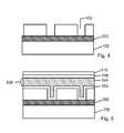
In a specific embodiment, the method forms a thirddielectric material 702 overlying the first structure and fills a gap region between the first structures as shown inFIG. 7 . The third dielectric material can be silicon oxide, silicon nitride, a multilayer dielectric stack having alternating layers of silicon oxide and silicon nitride (for example, an ONO stack), a high K dielectric, or a low K dielectric including a combination. The third dielectric material may be subjected to a planarizing process to form a planarized surface in certain embodiment. The planarization process can be an etch back process or a chemical mechanical polishing process or a combination, depending on the application. As shown, each of the switching element is isolated by the third dielectric material and disturbs between neighboring switching element is thus inhibited. As shown inFIG. 7 a, the method includes depositing anadhesion material 704 overlying the third dielectric material.Adhesion material 704 can be titanium, titanium nitride, tantalum nitride, tungsten nitride depending on the application.
Referring toFIG. 8 . The method includes subjectingadhesion material 704 and the third dielectric material to a third patterning and etch process to form a plurality of viaopenings 802 in portions of the third dielectric material and to expose asurface region 804 of the switching material in each of the first structure.
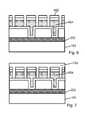
Depending on the embodiment, there can be other variations. For example, asidewall spacer structure 806 can be formed overlying a portion of each of the plurality of via opening as shown inFIG. 8( a). The sidewall spacer structure is formed by depositing a suitable dielectric material followed by a patterning and etching process. The dielectric material can be silicon nitride, silicon oxide and the like, depending on the embodiment.
As shown inFIG. 9 , the method includes depositing asecond wiring material 902 overlying the adhesion material and the third dielectric material and to fill each of the plurality of via openings. The second wiring material is a silver material in a specific embodiment. The silver material can be deposited using techniques such as a chemical vapor deposition process, a physical vapor deposition process, an electroplating process, an electroless deposition process, including any combination of theses, and others. In some embodiments, the silver material is in direct contact with the amorphous silicon in a specific embodiment. In other embodiments, a thin layer of oxide, is formed prior to the deposition of the silver material on top of the amorphous silicon. This interposing thin layer of oxide may be naturally or specifically grown or formed, and one or more etch operations (e.g. HF etch, Argon etch) may help control the thickness of this oxide layer. In some embodiments, the thickness of the oxide prior to deposition of the silver material may range from about 20 angstroms to about 50 angstroms; in other embodiments, the thickness may range from about 30 angstroms to about 40 angstroms; or the like.FIG. 9( a) illustrates the embodiment having the sidewall spacer structure.
The method subjects the second wiring material to a fourth patterning andetching process 1002 to form a plurality ofsecond wiring structure 1004 while the second wiring material remains in contact with the switching material. Prior to the fourth patterning and etching process, an anti-reflective coating (commonly called ARC) is deposited on the second wiring material to reduce reflection from a highly reflective, for example, silver surface. The antireflective coating can include titanium nitride, or silicon oxynitride, or others, depending on the embodiment. In a specific embodiment, the second wiring structure is spatially configured to extend in a second direction at an angle to the first direction. In a specific embodiment, the second direction is orthogonal to the first direction. As shown, aswitching region 1006 comprising the amorphous silicon material is formed in an intersection region between the first wiring structure and the second wiring structure in a crossbar manner in a specific embodiment. A corresponding structure having side wall structure is illustrated inFIG. 10( a).
For amorphous silicon material as the switching material, the silver material forms a silver region in a portion of the amorphous silicon material when a positive bias voltage greater than a forming voltage is applied to the top wiring structure. The use of the silver material as the top wiring structure thus eliminate an additional step of metal deposition and simplify process. Additional advantage of using silver as the top wiring structure is low resistivity and a smaller thickness needed to form interconnects, among others. After forming, the device is in at a high resistance state or an off state, and an off state current Ioffflows in the device. The silver region further comprises a silver filament characterized by a length and a distance between silver particles. The length of the silver filament depends at least on an operating voltage of the resistive switching device. When a write voltage is applied, the filament extends and the device is in a low resistance state or an on state, and an on state current Ionflows in the device. The filament retracts when an erase voltage having an opposite polarity to the write voltage is applied and the device is caused to revert back to the high resistance state. To perform a read operation, a read voltage is applied, a read current is measured, and the resistance state of the device can be determined.
Referring again toFIG. 9( a), the sidewall spacer structure effectively reduces an active device area for the non-volatile memory device. As off state current is essentially dominated by a leakage current through the amorphous silicon switching layer, a smaller device area would improve an Ion/Ioffratio and improves a signal to noise ratio for selected device in a read operation. This enables a high density array of devices and reduces cost of fabrication. Of course one skilled in the art would recognize other variations, modifications, and alternatives.
The above sequence of steps provides a method to form a crossbar array of memory cells overlying a substrate according to embodiments of the present invention. Each of the top wiring structure and the bottom wiring structure can be further extend into respectively a first periphery region and a second periphery region to connect to their respective control circuitry configured on the substrate in a specific embodiment. Depending on the application, one or more steps may be added, one or more steps may be omitted, or one or more step may be provided in a different sequence. One skilled in the art would recognize other variations, modifications, and alternatives.
In a specific embodiment, a method for forming a multilayer memory device is provided. Depending on the application, the multilayer memory device can have one to eight of crossbar arrays of memory cells. The method includes providing a substrate having a surface region. The substrate can be a single crystal silicon, silicon germanium, or a silicon on insulator (commonly known as SOI) substrate. In a specific embodiment, the semiconductor substrate can further include one or more transistor devices formed thereon. The one or more transistor devices provide controlling circuitry for the memory device in a specific embodiment.
The method forms a first dielectric material overlying the semiconductor substrate. The first dielectric material can be silicon oxide, silicon nitride, multilayer stack of alternating dielectric materials such as an alternating layers of silicon oxide on silicon nitride on silicon oxide (commonly known as ONO), high K dielectric, low K dielectric, and others.
The method includes forming a first crossbar array of memory cells overlying the first dielectric material using substantially the same steps for forming a single layer of crossbar array of memory cells. The first crossbar array of memory cells includes a first bottom wiring structure configured to spatially extend in a first direction. The first bottom wiring structure includes a silver material in a specific embodiment. The method includes forming a first switching region overlying the first bottom wiring structure. The first switching region includes an amorphous silicon material in a specific embodiment. A first top wiring structure is formed overlying at least the amorphous silicon switching region. The first top wiring structure includes a silver material in a specific embodiment. The first top wiring structure is configured to spatially extend in a second direction orthogonal to the first direction in a specific embodiment. The first switching region is configured to formed in an intersecting region of sandwiched between the first top wiring structure and the first top wiring structure in a specific embodiment.
The method includes forming a second dielectric material overlying the first top wiring structure of the first crossbar array of memory cells. A second crossbar array of memory cells are formed overlying the second dielectric material using substantially the same steps as for the first crossbar array of memory cells. The second crossbar array of memory cells includes a second bottom wiring structure configured to spatially extend and parallel in the first direction. The first bottom wiring structure includes a silver material in a specific embodiment. The method includes forming a second switching region overlying the second bottom wiring structure. The second switching region includes an amorphous silicon material in a specific embodiment. A second top wiring structure is formed overlying at least the amorphous silicon switching region. The second top wiring structure includes a silver material in a specific embodiment. The second top wiring structure is configured to spatially extend and parallel to the second direction orthogonal to the first direction in a specific embodiment. The second switching region is configured to formed in an intersecting region of sandwiched between the second top wiring structure and the second top wiring structure in a specific embodiment. The method can continue to form a third dielectric material overlying the second crossbar array of memory cells and a third crossbar array of memory cells overlying the third dielectric material in a same manner as forming the second crossbar array of memory cells. Depending on the embodiment, N crossbar arrays of memory cells can be formed, where is an integer ranging from one to eight. Each of the Nth crossbar array of memory cells is isolated from an (N−1)th crossbar array of memory cells by an Nth dielectric material in a specific embodiment.
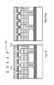
Referring toFIG. 11 , a four crossbar arrays of memory cells vertically stacked is illustrated. As shown the four crossbar arrays of memory cells include asubstrate 1102. The substrate can be a semiconductor substrate. In a specific embodiment, the substrate can have one or more controlling transistors formed thereon. Aninterconnect 1104 from the one or more controlling transistors is show. Afirst dielectric material 1106 overliesinterconnect 1104. A first crossbar array ofmemory cells 1108 overlies the first dielectric material. A second crossbar array ofmemory cells 1110, a third crossbar array ofmemory cells 1112, and a fourth crossbar array ofmemory cells 1114 are illustrated. The second crossbar array of memory cells are isolated from the first crossbar array of memory cells bydielectric material 1116. The third crossbar array of memory cells are isolated from the second crossbar array of memory cells bydielectric material 1110. The fourth crossbar array of memory cells are isolated from the third crossbar array of memory cells bydielectric material 1120. Also illustrated inFIG. 11 , each of the respectivetop wiring structures 1124 comprising a silver material extends to aperipheral region 1122 and connected to theirrespective control circuits 1126 on the substrate using their respectivevertical interconnect 1128.
Embodiments according to the present invention provides a method and a structure for a multilayer crossbar arrays of memory cells vertically stacked using a silver material for interconnects. Silver material as interconnects reduces resistivity of the interconnects and simplifies process, enhances device performance and improves device yield.
Though the present invention has been described using various examples and embodiments, it is also understood that the examples and embodiments described herein are for illustrative purposes only and that various modifications or alternatives in light thereof will be suggested to persons skilled in the art and are to be included within the spirit and purview of this application and scope of the appended claims.
Claims (21)
1. A method of forming a memory device, comprising:
providing a substrate having a surface region;
forming a first thickness of dielectric material overlying the surface region;
subjecting the first thickness of dielectric material to a first patterning and etching process to form a first opening structure in a portion of the first thickness of dielectric material;
depositing a first wiring material comprising at least a silver material to fill the opening structure and forming a thickness of the first wiring material overlying the first dielectric material;
depositing a switching material comprising an amorphous silicon material overlying the first wiring material;
subjecting at least the switching material and the thickness of the first wiring material to a first patterning and etching process to form one or more first structures, the first structures comprising a switching element and a first wiring structure comprising at least the first silver material, the first wiring structure being elongated in shape and spatially configured to extend in a first direction;
depositing a second thickness of dielectric material overlying the one or more first structures;
forming a via opening in the second thickness of dielectric material overlying at least a first portion of the switching element in each of the one or more first structure; and
forming a second wiring structure overlying the switching element, the second wiring structure comprising at least a second silver material and having a first portion in the via and being in electrical contact with at least a second the portion of the switching element, and a second portion elongated in shape and spatially configured to extend in a second direction orthogonal to the first direction.
2. The method ofclaim 1 further comprising depositing a first lining material overlying the first opening structure, the first lining material is selected from a group consisting of: titanium, titanium nitride, tantalum nitride, or tungsten nitride, and a combination thereof.
3. The method ofclaim 1 further comprising depositing a first adhesion material overlying the first wiring material, the first adhesion material selected from a group consisting of: titanium, titanium nitride, tantalum nitride, or tungsten nitride, and a combination thereof.
4. The method ofclaim 2 wherein the first lining material further comprises a dielectric diffusion barrier material; and
wherein the dielectric diffusion barrier material comprises a silicon carbide material.
5. The method ofclaim 2 wherein the first structure comprises a switching region, the switching region comprises the amorphous silicon material.
6. The method ofclaim 2 further comprising forming a dielectric spacer structure overlying within the via.
7. The method ofclaim 1 wherein the first silver material is deposited using a physical vapor deposition process or an electrochemical deposition method including electroplating and electroless deposition or a damascene process, and any combination of these.
8. The method ofclaim 1 wherein the semiconductor substrate is a material selected from a group consisting of: single crystal silicon wafer, silicon on insulator substrate, silicon germanium, or a combination.
9. The method ofclaim 1 wherein the first thickness of dielectric material is selected from a group consisting of: silicon oxide, silicon nitride, a high K dielectric, a low K dielectric, a multilayer dielectric stack, or a combination.
10. The method ofclaim 1 wherein the second silver material forms a silver region in a portion of the switching element upon application of a forming voltage greater than a threshold voltage.
11. The method ofclaim 1 further comprising forming a contact material interposed between the switching material and the first wiring material,
wherein the contact material comprises a p+ polysilicon material, wherein the p+ polysilicon material is configured to reduce a defect density at an interface region between the p+ polysilicon material and the first wiring material.
12. A non-volatile memory device structure, comprising:
a semiconductor substrate comprising a surface region;
a first dielectric material overlying the surface region of the semiconductor substrate;
a bottom wiring structure comprising at least a first silver material overlying the first dielectric material, the bottom wiring structure being configured to spatially extend in a first direction;
a contact material comprising a p+ polysilicon material overlying the bottom wiring structure;
a switching material comprising an amorphous silicon material overlying the contact material; and
a top wiring structure comprising at least a second silver material overlying the switching material, the top wiring structure comprising a first portion of the second silver material disposed in a via structure in direct contact with the switching material and a second portion configured to spatially extend in a second direction orthogonal to the first direction.
13. The device ofclaim 12 wherein the semiconductor substrate is a material selected from a group consisting of: single crystal silicon, silicon germanium, or silicon on insulator (SOI).
14. The device ofclaim 12 wherein the switching material forms a switching region in an intersecting region of at least a portion of the top wiring structure and at least a portion of the bottom wiring structure.
15. The device ofclaim 12 wherein the second silver material forms a silver region in a portion of the amorphous silicon material upon application of a threshold voltage greater than a forming voltage.
16. The device ofclaim 12 wherein the via structure comprises a via opening comprising a dielectric sidewall structure.
17. A memory device; comprising
a semiconductor substrate having a surface region;
a first dielectric material overlying the semiconductor substrate;
a first crossbar array of memory cells, comprising a first bottom wiring structure comprising a first silver material spatially extending in a first direction, a first top wiring structure comprising a second silver material spatially extending in a second direction orthogonal to the first direction, and a first switching region comprising an amorphous silicon material disposed between the first wiring structure and the second wiring structure;
a second dielectric material overlying the first crossbar array of memory cells; and
a second crossbar array of memory cells overlying the second dielectric material, the second crossbar array of memory cells comprising a second bottom wiring structure comprising a third silver material spatially extending in the first direction; a second top wiring structure comprising a fourth silver material spatially extending in the second direction, and a second switching region disposed between the second bottom wiring structure and the second top wiring structure.
18. The device ofclaim 17 wherein the first top wiring structure comprises a first portion having a first portion and a second portion, the first portion is disposed in a via structure overlying the first switching region, the second portion is elongated in shape and spatially configured to extend in the second direction.
19. The device ofclaim 17 wherein the second top wiring structure comprises a first portion having a first portion and a second portion, the first portion is disposed in a via structure overlying the second switching region, the second portion is elongated in shape and spatially configured to extend in the second direction.
20. The device ofclaim 17 further comprising a third dielectric material overlying the second crossbar array of memory cells and a third crossbar array of memory cells overlying the third dielectric material.
21. The device ofclaim 17 further comprising an Nth dielectric material overlying the (N−1)th crossbar array of memory cells and an Nth crossbar array of memory cells overlying the Nth dielectric material, where N is an integer ranging from 1 to 8.
Priority Applications (1)
| Application Number | Priority Date | Filing Date | Title |
|---|---|---|---|
| US13/339,851US8791010B1 (en) | 2010-12-31 | 2011-12-29 | Silver interconnects for stacked non-volatile memory device and method |
Applications Claiming Priority (2)
| Application Number | Priority Date | Filing Date | Title |
|---|---|---|---|
| US201061428982P | 2010-12-31 | 2010-12-31 | |
| US13/339,851US8791010B1 (en) | 2010-12-31 | 2011-12-29 | Silver interconnects for stacked non-volatile memory device and method |
Publications (1)
| Publication Number | Publication Date |
|---|---|
| US8791010B1true US8791010B1 (en) | 2014-07-29 |
Family
ID=51212079
Family Applications (1)
| Application Number | Title | Priority Date | Filing Date |
|---|---|---|---|
| US13/339,851Expired - Fee RelatedUS8791010B1 (en) | 2010-12-31 | 2011-12-29 | Silver interconnects for stacked non-volatile memory device and method |
Country Status (1)
| Country | Link |
|---|---|
| US (1) | US8791010B1 (en) |
Cited By (3)
| Publication number | Priority date | Publication date | Assignee | Title |
|---|---|---|---|---|
| US20160056206A1 (en)* | 2014-08-25 | 2016-02-25 | HGST, Inc. | 3-d planes memory device |
| US9425097B1 (en)* | 2015-04-29 | 2016-08-23 | Globalfoundries Inc. | Cut first alternative for 2D self-aligned via |
| US20190164597A1 (en)* | 2017-11-29 | 2019-05-30 | International Business Machines Corporation | Synaptic crossbar memory array |
Citations (205)
| Publication number | Priority date | Publication date | Assignee | Title |
|---|---|---|---|---|
| US680652A (en) | 1897-11-08 | 1901-08-13 | Leonard L Elden | Circuit-breaker. |
| US4433468A (en) | 1980-03-26 | 1984-02-28 | Nippon Electric Co., Ltd. | Method for making semiconductor device having improved thermal stress characteristics |
| US4684972A (en) | 1981-08-07 | 1987-08-04 | The British Petroleum Company, P.L.C. | Non-volatile amorphous semiconductor memory device utilizing a forming voltage |
| US4741601A (en) | 1984-10-08 | 1988-05-03 | Nec Corporation | Non-linear device for driving liquid crystal display |
| US5139911A (en) | 1989-01-04 | 1992-08-18 | Fuji Xerox Co., Ltd. | Electrophotographic photoreceptor with two part surface layer |
| US5242855A (en) | 1991-09-30 | 1993-09-07 | Nec Corporation | Method of fabricating a polycrystalline silicon film having a reduced resistivity |
| US5278085A (en) | 1992-08-11 | 1994-01-11 | Micron Semiconductor, Inc. | Single mask process for forming both n-type and p-type gates in a polycrystalline silicon layer during the formation of a semiconductor device |
| US5315131A (en) | 1990-11-22 | 1994-05-24 | Matsushita Electric Industrial Co., Ltd. | Electrically reprogrammable nonvolatile memory device |
| US5335219A (en) | 1991-01-18 | 1994-08-02 | Ovshinsky Stanford R | Homogeneous composition of microcrystalline semiconductor material, semiconductor devices and directly overwritable memory elements fabricated therefrom, and arrays fabricated from the memory elements |
| US5360981A (en) | 1989-05-11 | 1994-11-01 | British Telecommunications Public Limited Company | Amorphous silicon memory |
| US5457649A (en) | 1994-08-26 | 1995-10-10 | Microchip Technology, Inc. | Semiconductor memory device and write-once, read-only semiconductor memory array using amorphous-silicon and method therefor |
| US5538564A (en) | 1994-03-18 | 1996-07-23 | Regents Of The University Of California | Three dimensional amorphous silicon/microcrystalline silicon solar cells |
| US5541869A (en) | 1991-10-22 | 1996-07-30 | British Telecommunications, Plc | Resistive memory element |
| US5594363A (en) | 1995-04-07 | 1997-01-14 | Zycad Corporation | Logic cell and routing architecture in a field programmable gate array |
| US5614756A (en) | 1990-04-12 | 1997-03-25 | Actel Corporation | Metal-to-metal antifuse with conductive |
| US5707487A (en) | 1991-01-22 | 1998-01-13 | Kabushiki Kaisha Toshiba | Method of manufacturing semiconductor device |
| US5751012A (en) | 1995-06-07 | 1998-05-12 | Micron Technology, Inc. | Polysilicon pillar diode for use in a non-volatile memory cell |
| US5840608A (en) | 1996-11-22 | 1998-11-24 | United Microelectronics Corporation | High density ROM and a method of making the same |
| US5970332A (en) | 1995-03-28 | 1999-10-19 | U.S. Philips Corporation | Method of manufacturing a semiconductor device with a BiCMOS circuit |
| US5998244A (en) | 1996-08-22 | 1999-12-07 | Micron Technology, Inc. | Memory cell incorporating a chalcogenide element and method of making same |
| US6128214A (en) | 1999-03-29 | 2000-10-03 | Hewlett-Packard | Molecular wire crossbar memory |
| US6143642A (en) | 1997-12-22 | 2000-11-07 | Vlsi Technology, Inc. | Programmable semiconductor structures and methods for making the same |
| US6259116B1 (en) | 1997-10-22 | 2001-07-10 | U.S. Philips Corporation | Multiple memory element semiconductor memory devices |
| US6291836B1 (en) | 1996-06-05 | 2001-09-18 | U. S. Philips Corporation | Method of operating a programmable, non-volatile memory device |
| US6436818B1 (en) | 1997-02-19 | 2002-08-20 | Micron Technology, Inc. | Semiconductor structure having a doped conductive layer |
| US6436765B1 (en) | 2001-02-09 | 2002-08-20 | United Microelectronics Corp. | Method of fabricating a trenched flash memory cell |
| US6492694B2 (en) | 1998-02-27 | 2002-12-10 | Micron Technology, Inc. | Highly conductive composite polysilicon gate for CMOS integrated circuits |
| US20030052330A1 (en) | 2001-09-20 | 2003-03-20 | Klein Rita J. | Electro-and electroless plating of metal in the manufacture of PCRAM devices |
| WO2003034498A1 (en) | 2001-10-16 | 2003-04-24 | Midwest Research Institute | Stacked switchable element and diode combination |
| US6627530B2 (en) | 2000-12-22 | 2003-09-30 | Matrix Semiconductor, Inc. | Patterning three dimensional structures |
| US20040026682A1 (en) | 2002-06-17 | 2004-02-12 | Hai Jiang | Nano-dot memory and fabricating same |
| US6762474B1 (en) | 1998-06-10 | 2004-07-13 | Agere Systems Inc. | Method and apparatus for temperature compensation of read-only memory |
| US6768157B2 (en) | 2001-08-13 | 2004-07-27 | Advanced Micro Devices, Inc. | Memory device |
| US20040170040A1 (en) | 2002-08-02 | 2004-09-02 | Unity Semiconductor Corporation | Rewritable memory with non-linear memory element |
| US20040192006A1 (en) | 2002-02-20 | 2004-09-30 | Campbell Kristy A. | Layered resistance variable memory device and method of fabrication |
| US20040194340A1 (en) | 1998-10-14 | 2004-10-07 | Tokyo Electron Limited | Method and apparatus for surface treatment |
| US6815286B2 (en) | 2001-08-13 | 2004-11-09 | Advanced Micro Devices, Inc. | Memory device |
| US6838720B2 (en) | 2001-08-13 | 2005-01-04 | Advanced Micro Devices, Inc. | Memory device with active passive layers |
| US20050020510A1 (en) | 2002-08-29 | 2005-01-27 | Benedict Dale L. | D-mannose contraceptives |
| US20050029587A1 (en) | 1995-06-07 | 2005-02-10 | Harshfield Steven T. | Method and apparatus for forming an integrated circuit electrode having a reduced contact area |
| US6858482B2 (en) | 2002-04-10 | 2005-02-22 | Micron Technology, Inc. | Method of manufacture of programmable switching circuits and memory cells employing a glass layer |
| US6858481B2 (en) | 2001-08-13 | 2005-02-22 | Advanced Micro Devices, Inc. | Memory device with active and passive layers |
| US6864127B2 (en) | 1997-04-25 | 2005-03-08 | Semiconductor Energy Laboratory Co., Ltd. | Semiconductor device and method of fabricating the same |
| US20050052915A1 (en) | 2002-12-19 | 2005-03-10 | Matrix Semiconductor, Inc. | Nonvolatile memory cell without a dielectric antifuse having high- and low-impedance states |
| US20050062045A1 (en) | 2002-10-02 | 2005-03-24 | Arup Bhattacharyya | Processes of forming stacked resistor constructions |
| US20050073881A1 (en) | 2003-10-06 | 2005-04-07 | Tran Lung The | Magnetic memory device including groups of series-connected memory elements |
| US6881994B2 (en) | 2000-08-14 | 2005-04-19 | Matrix Semiconductor, Inc. | Monolithic three dimensional array of charge storage devices containing a planarized surface |
| US6939787B2 (en) | 1999-12-28 | 2005-09-06 | Fujitsu Limited | Method for fabricating semiconductor device having gate electrode with polymetal structure of polycrystalline silicon film and metal film |
| US6946719B2 (en) | 2003-12-03 | 2005-09-20 | Matrix Semiconductor, Inc | Semiconductor device including junction diode contacting contact-antifuse unit comprising silicide |
| US20060017488A1 (en) | 2004-07-21 | 2006-01-26 | Sharp Laboratories Of America, Inc. | Mono-polarity switchable PCMO resistor trimmer |
| US7020006B2 (en) | 2002-08-02 | 2006-03-28 | Unity Semiconductor Corporation | Discharge of conductive array lines in fast memory |
| US7023093B2 (en) | 2002-10-24 | 2006-04-04 | International Business Machines Corporation | Very low effective dielectric constant interconnect Structures and methods for fabricating the same |
| US7102150B2 (en) | 2001-05-11 | 2006-09-05 | Harshfield Steven T | PCRAM memory cell and method of making same |
| US7122853B1 (en) | 2004-08-17 | 2006-10-17 | Fasl, Inc. | Method to improve yield and simplify operation of polymer memory cells |
| US20060281244A1 (en) | 2005-06-08 | 2006-12-14 | Masayuki Ichige | Nonvolatile semiconductor memory device and method of manufacturing the same |
| US20070008773A1 (en) | 2005-07-11 | 2007-01-11 | Matrix Semiconductor, Inc. | Nonvolatile memory cell comprising switchable resistor and transistor |
| US20070015348A1 (en) | 2005-07-18 | 2007-01-18 | Sharp Laboratories Of America, Inc. | Crosspoint resistor memory device with back-to-back Schottky diodes |
| US20070045615A1 (en) | 2005-08-31 | 2007-03-01 | Samsung Electronics Co., Ltd. | Non-volatile organic resistance random access memory device and method of manufacturing the same |
| US7187577B1 (en) | 2005-11-23 | 2007-03-06 | Grandis, Inc. | Method and system for providing current balanced writing for memory cells and magnetic devices |
| US20070087508A1 (en) | 2003-12-03 | 2007-04-19 | Herner S B | Method for making a p-i-n diode crystallized adjacent to a silicide in series with a dielectric antifuse |
| US20070090425A1 (en) | 2005-09-28 | 2007-04-26 | Matrix Semiconductor, Inc. | Memory cell comprising switchable semiconductor memory element with trimmable resistance |
| US20070105284A1 (en) | 2003-12-03 | 2007-05-10 | Herner S B | Method for forming a memory cell comprising a semiconductor junction diode crystallized adjacent to a silicide |
| US20070105390A1 (en) | 2005-11-09 | 2007-05-10 | Oh Travis B | Oxygen depleted etching process |
| US7221599B1 (en) | 2004-11-01 | 2007-05-22 | Spansion, Llc | Polymer memory cell operation |
| US7238607B2 (en) | 2002-12-19 | 2007-07-03 | Sandisk 3D Llc | Method to minimize formation of recess at surface planarized by chemical mechanical planarization |
| US20070205510A1 (en) | 2006-03-03 | 2007-09-06 | Lavoie Adrien R | Noble metal barrier layers |
| US20070228414A1 (en) | 2006-03-31 | 2007-10-04 | Sandisk 3D, Llc | Heterojunction device comprising a semiconductor and a resistivity-switching oxide or nitride |
| JP2007281208A (en) | 2006-04-07 | 2007-10-25 | Matsushita Electric Ind Co Ltd | Multilayer variable resistance element array, variable resistance device, multilayer nonvolatile memory element array, and nonvolatile memory device |
| US7289353B2 (en) | 2004-08-17 | 2007-10-30 | Spansion, Llc | Systems and methods for adjusting programming thresholds of polymer memory cells |
| US20070284575A1 (en) | 2005-07-18 | 2007-12-13 | Sharp Laboratories Of America, Inc. | Metal/semiconductor/metal current limiter |
| JP2007328857A (en) | 2006-06-07 | 2007-12-20 | Sony Corp | Storage device |
| US20070290186A1 (en) | 2006-05-04 | 2007-12-20 | El Mostafa Bourim | Non-volatile variable resistance memory device and method of fabricating the same |
| US20070295950A1 (en) | 2006-06-27 | 2007-12-27 | Samsung Electronics Co., Ltd. | Variable resistance random access memory device and a method of fabricating the same |
| US20080002481A1 (en) | 2002-12-20 | 2008-01-03 | Dietmar Gogl | Integrated Circuit, Method of Operating an Integrated Circuit, Method of Manufacturing an Integrated Circuit, Memory Module, Stackable Memory Module |
| US20080006907A1 (en) | 2006-07-06 | 2008-01-10 | Samsung Electronics Co., Ltd | Non-volatile memory device including a variable resistance material |
| US7324363B2 (en) | 2005-12-12 | 2008-01-29 | Synopsys, Inc. | SPICE optimized for arrays |
| US20080048164A1 (en) | 2006-07-11 | 2008-02-28 | Matsushita Electric Industrial Co., Ltd. | Electro-resistance element, method of manufacturing the same and electro-resistance memory using the same |
| US20080089110A1 (en) | 2006-10-16 | 2008-04-17 | Warren Robinett | Crossbar-memory systems and methods for writing to and reading from crossbar memory junctions of crossbar-memory systems |
| US20080090337A1 (en) | 2006-10-03 | 2008-04-17 | Williams R Stanley | Electrically actuated switch |
| US7365411B2 (en) | 2004-08-12 | 2008-04-29 | Micron Technology, Inc. | Resistance variable memory with temperature tolerant materials |
| US20080106925A1 (en) | 2006-11-08 | 2008-05-08 | Symetrix Corporation | Correlated electron memory |
| US20080106926A1 (en) | 2006-11-08 | 2008-05-08 | Symetrix Corporation | Non-volatile resistance switching memories and methods of making same |
| US7405418B2 (en) | 2004-02-17 | 2008-07-29 | Infineon Technologies Ag | Memory device electrode with a surface structure |
| US20080185567A1 (en) | 2007-02-05 | 2008-08-07 | Nitin Kumar | Methods for forming resistive switching memory elements |
| US20080205179A1 (en) | 2007-02-28 | 2008-08-28 | Qimonda Ag | Integrated circuit having a memory array |
| US20080206931A1 (en) | 2002-07-26 | 2008-08-28 | Laurent Breuil | Nonvolatile memory element and production method thereof and storage memory arrangement |
| US20080220601A1 (en) | 2007-03-05 | 2008-09-11 | Nitin Kumar | Methods for forming nonvolatile memory elements with resistive-switching metal oxides |
| US20080232160A1 (en) | 2007-02-27 | 2008-09-25 | International Business Machines Corporation | Rectifying element for a crosspoint based memory array architecture |
| US20080278990A1 (en) | 2007-05-09 | 2008-11-13 | Pragati Kumar | Resistive-switching nonvolatile memory elements |
| US20080304312A1 (en) | 2007-06-11 | 2008-12-11 | Macronix International Co., Ltd. | Resistance memory with tungsten compound and manufacturing |
| US20080311722A1 (en) | 2007-06-15 | 2008-12-18 | Sandisk 3D Llc | Method for forming polycrystalline thin film bipolar transistors |
| US20090001345A1 (en) | 2007-06-29 | 2009-01-01 | April Schricker | Memory cell that employs a selectively deposited reversible resistance-switching element and methods of forming the same |
| US7474000B2 (en) | 2003-12-05 | 2009-01-06 | Sandisk 3D Llc | High density contact to relaxed geometry layers |
| WO2009005699A1 (en) | 2007-06-29 | 2009-01-08 | Sandisk 3D, Llc | Memory cell that employs a selectively grown reversible resistance-switching element and methods of forming the same |
| US20090014707A1 (en) | 2006-10-20 | 2009-01-15 | Wei Lu | Non-volatile solid state resistive switching devices |
| US20090052226A1 (en) | 2007-08-24 | 2009-02-26 | Samsung Electronics Co., Ltd | Resistive random access memory device |
| US20090095951A1 (en) | 2007-10-12 | 2009-04-16 | Ovonyx, Inc. | Memory Device With Low Reset Current |
| US7521705B2 (en) | 2005-08-15 | 2009-04-21 | Micron Technology, Inc. | Reproducible resistance variable insulating memory devices having a shaped bottom electrode |
| US7534625B2 (en) | 2004-09-24 | 2009-05-19 | Karpov Ilya V | Phase change memory with damascene memory element |
| US7541252B2 (en) | 2006-11-09 | 2009-06-02 | Samsung Electronics Co., Ltd. | Methods of fabricating a semiconductor device including a self-aligned cell diode |
| US20090152737A1 (en) | 2000-07-14 | 2009-06-18 | Micron Technology, Inc. | Memory devices having contact features |
| US7550380B2 (en) | 2004-11-03 | 2009-06-23 | Micron Technology, Inc. | Electroless plating of metal caps for chalcogenide-based memory devices |
| US20090168486A1 (en) | 2007-12-27 | 2009-07-02 | Sandisk 3D Llc | Large capacity one-time programmable memory cell using metal oxides |
| US20090231910A1 (en) | 2008-03-11 | 2009-09-17 | Micron Technology, Inc. | Non-volatile memory with resistive access component |
| US20090257265A1 (en) | 2008-04-11 | 2009-10-15 | Sandisk 3D Llc | Multilevel nonvolatile memory device containing a carbon storage material and methods of making and using same |
| US20090256130A1 (en) | 2008-04-11 | 2009-10-15 | Sandisk 3D Llc | Memory cell that employs a selectively fabricated carbon nano-tube reversible resistance-switching element, and methods of forming the same |
| US7606059B2 (en) | 2003-03-18 | 2009-10-20 | Kabushiki Kaisha Toshiba | Three-dimensional programmable resistance memory device with a read/write circuit stacked under a memory cell array |
| US20090267047A1 (en) | 2008-04-28 | 2009-10-29 | Hitachi, Ltd. | Semiconductor memory device and manufacturing method thereof |
| US7615439B1 (en) | 2008-09-29 | 2009-11-10 | Sandisk Corporation | Damascene process for carbon memory element with MIIM diode |
| US20090298224A1 (en) | 2002-12-13 | 2009-12-03 | Lowrey Tyler A | Memory and Access Device and Method Therefor |
| US20090321789A1 (en) | 2008-06-30 | 2009-12-31 | Sandisk 3D Llc | Triangle two dimensional complementary patterning of pillars |
| US20100007937A1 (en) | 2006-11-09 | 2010-01-14 | Sage Electrochromics, Inc. | Method of making an ion-switching device without a separate lithiation step |
| US20100012914A1 (en) | 2008-07-18 | 2010-01-21 | Sandisk 3D Llc | Carbon-based resistivity-switching materials and methods of forming the same |
| US20100019221A1 (en) | 2008-07-22 | 2010-01-28 | Macronix International Co., Ltd. | Fully self-aligned pore-type memory cell having diode access device |
| US20100019310A1 (en) | 2008-07-25 | 2010-01-28 | Kabushiki Kaisha Toshiba | Semiconductor memory device |
| US20100032638A1 (en) | 2008-08-07 | 2010-02-11 | Sandisk 3D Llc | Memory cell that includes a carbon-based memory element and methods of forming the same |
| US20100044708A1 (en) | 2008-08-19 | 2010-02-25 | Chunghwa Picture Tubes, Ltd. | Thin film transistor, pixel structure and fabrication methods thereof |
| US20100085798A1 (en) | 2008-10-08 | 2010-04-08 | The Regents Of The University Of Michigan | Silicon-based nanoscale resistive device with adjustable resistance |
| US20100084625A1 (en) | 2008-10-02 | 2010-04-08 | Guy Wicker | Memory Device |
| US20100090192A1 (en) | 2006-08-31 | 2010-04-15 | Nxp, B.V. | Method for controlled formation of the resistive switching material in a resistive switching device and device obtained thereof |
| US20100101290A1 (en) | 2008-10-24 | 2010-04-29 | Antonio Bertolotto | Method for the production of an agent for treatment of agricultural soils |
| US20100102290A1 (en) | 2008-10-20 | 2010-04-29 | The Regents Of The University Of Michigan | Silicon based nanoscale crossbar memory |
| US7729158B2 (en) | 2003-04-03 | 2010-06-01 | Kabushiki Kaisha Toshiba | Resistance change memory device |
| US7728318B2 (en) | 2006-11-16 | 2010-06-01 | Sandisk Corporation | Nonvolatile phase change memory cell having a reduced contact area |
| US20100157710A1 (en) | 2008-12-19 | 2010-06-24 | Unity Semiconductor Corporation | Array Operation Using A Schottky Diode As a Non-Ohmic Isolation Device |
| US20100157651A1 (en) | 2008-12-18 | 2010-06-24 | Sandisk 3D Llc | Method of programming a nonvolatile memory device containing a carbon storage material |
| US20100163828A1 (en) | 2008-12-30 | 2010-07-01 | Industrial Technology Research Institute | Phase change memory devices and methods for fabricating the same |
| US7749805B2 (en) | 2005-03-10 | 2010-07-06 | Qimonda Ag | Method for manufacturing an integrated circuit including an electrolyte material layer |
| US20100176368A1 (en) | 2009-01-14 | 2010-07-15 | Ko Nikka | Method of manufacturing semiconductor memory device, and semiconductor memory device |
| US7772581B2 (en) | 2006-09-11 | 2010-08-10 | Macronix International Co., Ltd. | Memory device having wide area phase change element and small electrode contact area |
| US7786464B2 (en) | 2007-11-20 | 2010-08-31 | Infineon Technologies Ag | Integrated circuit having dielectric layer including nanocrystals |
| US7786589B2 (en) | 2006-12-06 | 2010-08-31 | Kabushiki Kaisha Toshiba | Semiconductor device and method for manufacturing semiconductor device |
| US20100219510A1 (en) | 2008-06-30 | 2010-09-02 | Sandisk 3D Llc | Method for fabricating high density pillar structures by double patterning using positive photoresist |
| US20100221868A1 (en) | 2007-12-04 | 2010-09-02 | Regino Sandoval | Active Material Devices with Containment Layer |
| US7824956B2 (en) | 2007-06-29 | 2010-11-02 | Sandisk 3D Llc | Memory cell that employs a selectively grown reversible resistance-switching element and methods of forming the same |
| US7829875B2 (en) | 2006-03-31 | 2010-11-09 | Sandisk 3D Llc | Nonvolatile rewritable memory cell comprising a resistivity-switching oxide or nitride and an antifuse |
| US7835170B2 (en) | 2005-05-09 | 2010-11-16 | Nantero, Inc. | Memory elements and cross point switches and arrays of same using nonvolatile nanotube blocks |
| US20100321095A1 (en) | 2008-06-10 | 2010-12-23 | Takumi Mikawa | Semiconductor device, manufacturing method of semiconductor device, semiconductor chip and system |
| US7859884B2 (en) | 2005-01-19 | 2010-12-28 | Sandisk 3D Llc | Structure and method for biasing phase change memory array for reliable writing |
| US7858468B2 (en) | 2008-10-30 | 2010-12-28 | Micron Technology, Inc. | Memory devices and formation methods |
| US20110006275A1 (en) | 2009-07-13 | 2011-01-13 | Seagate Technology Llc | Non-volatile resistive sense memory |
| US7881097B2 (en) | 2006-12-26 | 2011-02-01 | Sony Corporation | Storage element and memory |
| US7898838B2 (en) | 2008-10-31 | 2011-03-01 | Seagate Technology Llc | Resistive sense memory calibration for self-reference read method |
| US7897953B2 (en) | 2008-01-16 | 2011-03-01 | Micron Technology, Inc. | Multi-level programmable PCRAM memory |
| US7920412B2 (en) | 2006-09-29 | 2011-04-05 | Kabushiki Kaisha Toshiba | Magnetic random access memory and method of manufacturing the same |
| US7924138B2 (en) | 2007-03-01 | 2011-04-12 | Fujitsu Limited | Semiconductor device and manufacturing method of the same |
| US20110089391A1 (en) | 2009-10-20 | 2011-04-21 | Andrei Mihnea | Punch-through diode steering element |
| US20110133149A1 (en) | 2009-12-04 | 2011-06-09 | Sonehara Takeshi | Resistance change memory and manufacturing method thereof |
| US20110136327A1 (en) | 2009-12-03 | 2011-06-09 | Applied Materials, Inc. | High mobility monolithic p-i-n diodes |
| US7968419B2 (en) | 2005-07-18 | 2011-06-28 | Sharp Laboratories Of America, Inc. | Back-to-back metal/semiconductor/metal (MSM) Schottky diode |
| US20110155991A1 (en) | 2009-12-29 | 2011-06-30 | Industrial Technology Research Institute | Resistive memory device and fabricating method thereof |
| US7984776B2 (en) | 2007-03-30 | 2011-07-26 | The Regents Of The University Of Michigan | Energy storage and control system for a vehicle electrified drivetrain |
| US20110194329A1 (en) | 2010-02-09 | 2011-08-11 | Sony Corporation | Memory component, memory device, and method of operating memory device |
| US20110198557A1 (en) | 2008-02-07 | 2011-08-18 | International Business Machines Corporation | Method for fabrication of crystalline diodes for resistive memories |
| US8004882B2 (en) | 2004-06-04 | 2011-08-23 | Micron Technology, Inc. | Spintronic devices with integrated transistors |
| US20110205782A1 (en) | 2010-02-23 | 2011-08-25 | Xiying Chen Costa | Step soft program for reversible resistivity-switching elements |
| US20110204312A1 (en) | 2008-05-10 | 2011-08-25 | Intermolecular, Inc. | Confinement techniques for non-volatile resistive-switching memories |
| US8018760B2 (en) | 2006-12-28 | 2011-09-13 | Panasonic Corporation | Resistance variable element and resistance variable memory apparatus |
| US8021897B2 (en) | 2009-02-19 | 2011-09-20 | Micron Technology, Inc. | Methods of fabricating a cross point memory array |
| US20110227028A1 (en) | 2010-03-16 | 2011-09-22 | Deepak Chandra Sekar | Bottom electrodes for use with metal oxide resistivity switching layers |
| US8045364B2 (en) | 2009-12-18 | 2011-10-25 | Unity Semiconductor Corporation | Non-volatile memory device ion barrier |
| US8054674B2 (en) | 2007-05-10 | 2011-11-08 | Sharp Kabushiki Kaisha | Variable resistive element, manufacturing method for same, and non-volatile semiconductor memory device |
| US20110284814A1 (en) | 2010-05-24 | 2011-11-24 | Guobiao Zhang | Large Bit-Per-Cell Three-Dimensional Mask-Programmable Read-Only Memory |
| US8067815B2 (en) | 2008-12-11 | 2011-11-29 | Macronix International Co., Lt.d. | Aluminum copper oxide based memory devices and methods for manufacture |
| US20110305064A1 (en) | 2010-06-11 | 2011-12-15 | Crossbar, Inc. | Interface control for improved switching in rram |
| US20110312151A1 (en) | 2010-06-11 | 2011-12-22 | Crossbar Inc. | Pillar structure for memory device and method |
| US20110317470A1 (en) | 2010-06-24 | 2011-12-29 | The Regents Of The University Of Michigan | Rectification element and method for resistive switching for non volatile memory device |
| US8088688B1 (en) | 2010-11-05 | 2012-01-03 | Crossbar, Inc. | p+ polysilicon material on aluminum for non-volatile memory device and method |
| US20120001145A1 (en) | 2008-12-31 | 2012-01-05 | Michele Magistretti | Avoiding degradation of chalcogenide material during definition of multilayer stack structure |
| EP2405441A1 (en) | 2010-07-09 | 2012-01-11 | Crossbar, Inc. | Resistive memory using SiGe material |
| US20120007035A1 (en) | 2010-07-12 | 2012-01-12 | Crossbar, Inc. | Intrinsic Programming Current Control for a RRAM |
| US8097874B2 (en) | 2008-10-30 | 2012-01-17 | Seagate Technology Llc | Programmable resistive memory cell with sacrificial metal |
| EP2408035A2 (en) | 2010-07-13 | 2012-01-18 | Crossbar, Inc. | Two terminal resistive switching device structure and method of fabricating |
| US20120012806A1 (en) | 2010-07-13 | 2012-01-19 | Crossbar, Inc. | Improved on/off ratio for non-volatile memory device and method |
| US20120012808A1 (en) | 2004-09-29 | 2012-01-19 | Herner S Brad | Deposited semiconductor structure to minimize n-type dopant diffusion and method of making |
| US20120025161A1 (en) | 2008-02-27 | 2012-02-02 | Manuj Rathor | Diode and resistive memory device structures |
| US20120033479A1 (en) | 2010-08-06 | 2012-02-09 | Lsi Corporation | Modification of logic by morphological manipulation of a semiconductor resistive element |
| US20120043519A1 (en) | 2010-08-23 | 2012-02-23 | Crossbar, Inc. | Device switching using layered device structure |
| US20120043621A1 (en) | 2010-08-23 | 2012-02-23 | Crossbar, Inc. | Stackable non-volatile resistive switching memory device and method |
| US20120043654A1 (en) | 2010-08-19 | 2012-02-23 | Taiwan Semiconductor Manufacturing Company, Ltd. | Mechanisms for forming copper pillar bumps using patterned anodes |
| US8143092B2 (en) | 2008-03-10 | 2012-03-27 | Pragati Kumar | Methods for forming resistive switching memory elements by heating deposited layers |
| US20120074507A1 (en) | 2010-09-29 | 2012-03-29 | Crossbar, Inc. | Integration of an amorphous silicon resistive switching device |
| US20120074374A1 (en) | 2010-09-29 | 2012-03-29 | Crossbar, Inc. | Conductive path in switching material in a resistive random access memory device and control |
| US20120108030A1 (en) | 2010-10-27 | 2012-05-03 | Crossbar, Inc. | Method for obtaining smooth, continuous silver film |
| US20120104351A1 (en) | 2010-07-01 | 2012-05-03 | Zhiqiang Wei | Non-volatile memory cell, non-volatile memory cell array, and method of manufacturing the same |
| US8183553B2 (en) | 2009-04-10 | 2012-05-22 | Intermolecular, Inc. | Resistive switching memory element including doped silicon electrode |
| US20120145984A1 (en) | 2010-12-13 | 2012-06-14 | Peter Rabkin | Punch-through diode |
| US20120155146A1 (en) | 2010-12-20 | 2012-06-21 | Yoshihiro Ueda | Resistance-change memory |
| US8207064B2 (en) | 2009-09-17 | 2012-06-26 | Sandisk 3D Llc | 3D polysilicon diode with low contact resistance and method for forming same |
| US8231998B2 (en) | 2007-03-30 | 2012-07-31 | The Regents Of The University Of Michigan | Deposited microarchitectured battery and manufacturing method |
| US8233308B2 (en) | 2007-06-29 | 2012-07-31 | Sandisk 3D Llc | Memory cell that employs a selectively deposited reversible resistance-switching element and methods of forming the same |
| US8237146B2 (en) | 2010-02-24 | 2012-08-07 | Sandisk 3D Llc | Memory cell with silicon-containing carbon switching layer and methods for forming the same |
| US20120205606A1 (en) | 2011-02-14 | 2012-08-16 | Dongguk University Industry-Academic Cooperation Foundation | Nonvolatile Memory Device Using The Resistive Switching of Graphene Oxide And The Fabrication Method Thereof |
| US8258020B2 (en) | 2010-11-04 | 2012-09-04 | Crossbar Inc. | Interconnects for stacked non-volatile memory device and method |
| US20120235112A1 (en) | 2010-11-30 | 2012-09-20 | Huo Zongliang | Resistive switching memory and method for manufacturing the same |
| US8274812B2 (en) | 2010-06-14 | 2012-09-25 | Crossbar, Inc. | Write and erase scheme for resistive memory device |
| US20120250183A1 (en) | 2011-03-31 | 2012-10-04 | Nidec Corporation | Motor and storage disk drive |
| US8315079B2 (en) | 2010-10-07 | 2012-11-20 | Crossbar, Inc. | Circuit for concurrent read operation and method therefor |
| US8320160B2 (en) | 2011-03-18 | 2012-11-27 | Crossbar, Inc. | NAND architecture having a resistive memory cell connected to a control gate of a field-effect transistor |
| US20120305874A1 (en) | 2011-05-31 | 2012-12-06 | Crossbar, Inc. | Vertical Diodes for Non-Volatile Memory Device |
| US8385100B2 (en) | 2009-12-08 | 2013-02-26 | Intel Corporation | Energy-efficient set write of phase change memory with switch |
| US8389971B2 (en) | 2010-10-14 | 2013-03-05 | Sandisk 3D Llc | Memory cells having storage elements that share material layers with steering elements and methods of forming the same |
| US8467227B1 (en) | 2010-11-04 | 2013-06-18 | Crossbar, Inc. | Hetero resistive switching material layer in RRAM device and method |
| US8658476B1 (en) | 2012-04-20 | 2014-02-25 | Crossbar, Inc. | Low temperature P+ polycrystalline silicon material for non-volatile memory device |
| US8659003B2 (en) | 2010-08-23 | 2014-02-25 | Crossbar, Inc. | Disturb-resistant non-volatile memory device and method |
- 2011
- 2011-12-29USUS13/339,851patent/US8791010B1/ennot_activeExpired - Fee Related
Patent Citations (238)
| Publication number | Priority date | Publication date | Assignee | Title |
|---|---|---|---|---|
| US680652A (en) | 1897-11-08 | 1901-08-13 | Leonard L Elden | Circuit-breaker. |
| US4433468A (en) | 1980-03-26 | 1984-02-28 | Nippon Electric Co., Ltd. | Method for making semiconductor device having improved thermal stress characteristics |
| US4684972A (en) | 1981-08-07 | 1987-08-04 | The British Petroleum Company, P.L.C. | Non-volatile amorphous semiconductor memory device utilizing a forming voltage |
| US4741601A (en) | 1984-10-08 | 1988-05-03 | Nec Corporation | Non-linear device for driving liquid crystal display |
| US5139911A (en) | 1989-01-04 | 1992-08-18 | Fuji Xerox Co., Ltd. | Electrophotographic photoreceptor with two part surface layer |
| US5360981A (en) | 1989-05-11 | 1994-11-01 | British Telecommunications Public Limited Company | Amorphous silicon memory |
| US5614756A (en) | 1990-04-12 | 1997-03-25 | Actel Corporation | Metal-to-metal antifuse with conductive |
| US5315131A (en) | 1990-11-22 | 1994-05-24 | Matsushita Electric Industrial Co., Ltd. | Electrically reprogrammable nonvolatile memory device |
| US5335219A (en) | 1991-01-18 | 1994-08-02 | Ovshinsky Stanford R | Homogeneous composition of microcrystalline semiconductor material, semiconductor devices and directly overwritable memory elements fabricated therefrom, and arrays fabricated from the memory elements |
| US5707487A (en) | 1991-01-22 | 1998-01-13 | Kabushiki Kaisha Toshiba | Method of manufacturing semiconductor device |
| US5242855A (en) | 1991-09-30 | 1993-09-07 | Nec Corporation | Method of fabricating a polycrystalline silicon film having a reduced resistivity |
| US5541869A (en) | 1991-10-22 | 1996-07-30 | British Telecommunications, Plc | Resistive memory element |
| US5278085A (en) | 1992-08-11 | 1994-01-11 | Micron Semiconductor, Inc. | Single mask process for forming both n-type and p-type gates in a polycrystalline silicon layer during the formation of a semiconductor device |
| US5538564A (en) | 1994-03-18 | 1996-07-23 | Regents Of The University Of California | Three dimensional amorphous silicon/microcrystalline silicon solar cells |
| US5457649A (en) | 1994-08-26 | 1995-10-10 | Microchip Technology, Inc. | Semiconductor memory device and write-once, read-only semiconductor memory array using amorphous-silicon and method therefor |
| US5714416A (en) | 1994-08-26 | 1998-02-03 | Microchip Technology Incorporated | Semiconductor memory device and write-once, read-only semiconductor memory array using amorphous-silicon and method therefor |
| US5970332A (en) | 1995-03-28 | 1999-10-19 | U.S. Philips Corporation | Method of manufacturing a semiconductor device with a BiCMOS circuit |
| US5594363A (en) | 1995-04-07 | 1997-01-14 | Zycad Corporation | Logic cell and routing architecture in a field programmable gate array |
| US5751012A (en) | 1995-06-07 | 1998-05-12 | Micron Technology, Inc. | Polysilicon pillar diode for use in a non-volatile memory cell |
| US20050029587A1 (en) | 1995-06-07 | 2005-02-10 | Harshfield Steven T. | Method and apparatus for forming an integrated circuit electrode having a reduced contact area |
| US6291836B1 (en) | 1996-06-05 | 2001-09-18 | U. S. Philips Corporation | Method of operating a programmable, non-volatile memory device |
| US5998244A (en) | 1996-08-22 | 1999-12-07 | Micron Technology, Inc. | Memory cell incorporating a chalcogenide element and method of making same |
| US5840608A (en) | 1996-11-22 | 1998-11-24 | United Microelectronics Corporation | High density ROM and a method of making the same |
| US6436818B1 (en) | 1997-02-19 | 2002-08-20 | Micron Technology, Inc. | Semiconductor structure having a doped conductive layer |
| US6864127B2 (en) | 1997-04-25 | 2005-03-08 | Semiconductor Energy Laboratory Co., Ltd. | Semiconductor device and method of fabricating the same |
| US6259116B1 (en) | 1997-10-22 | 2001-07-10 | U.S. Philips Corporation | Multiple memory element semiconductor memory devices |
| US6143642A (en) | 1997-12-22 | 2000-11-07 | Vlsi Technology, Inc. | Programmable semiconductor structures and methods for making the same |
| US6492694B2 (en) | 1998-02-27 | 2002-12-10 | Micron Technology, Inc. | Highly conductive composite polysilicon gate for CMOS integrated circuits |
| US6762474B1 (en) | 1998-06-10 | 2004-07-13 | Agere Systems Inc. | Method and apparatus for temperature compensation of read-only memory |
| US20040194340A1 (en) | 1998-10-14 | 2004-10-07 | Tokyo Electron Limited | Method and apparatus for surface treatment |
| US6128214A (en) | 1999-03-29 | 2000-10-03 | Hewlett-Packard | Molecular wire crossbar memory |
| US6939787B2 (en) | 1999-12-28 | 2005-09-06 | Fujitsu Limited | Method for fabricating semiconductor device having gate electrode with polymetal structure of polycrystalline silicon film and metal film |
| US20090152737A1 (en) | 2000-07-14 | 2009-06-18 | Micron Technology, Inc. | Memory devices having contact features |
| US20120080798A1 (en) | 2000-07-14 | 2012-04-05 | Round Rock Research, Llc | Memory devices having contact features |
| US6881994B2 (en) | 2000-08-14 | 2005-04-19 | Matrix Semiconductor, Inc. | Monolithic three dimensional array of charge storage devices containing a planarized surface |
| US6627530B2 (en) | 2000-12-22 | 2003-09-30 | Matrix Semiconductor, Inc. | Patterning three dimensional structures |
| US6436765B1 (en) | 2001-02-09 | 2002-08-20 | United Microelectronics Corp. | Method of fabricating a trenched flash memory cell |
| US7102150B2 (en) | 2001-05-11 | 2006-09-05 | Harshfield Steven T | PCRAM memory cell and method of making same |
| US6864522B2 (en) | 2001-08-13 | 2005-03-08 | Advanced Micro Devices, Inc. | Memory device |
| US6815286B2 (en) | 2001-08-13 | 2004-11-09 | Advanced Micro Devices, Inc. | Memory device |
| US6838720B2 (en) | 2001-08-13 | 2005-01-04 | Advanced Micro Devices, Inc. | Memory device with active passive layers |
| US7254053B2 (en) | 2001-08-13 | 2007-08-07 | Advanced Micro Devices, Inc. | Active programming and operation of a memory device |
| US6858481B2 (en) | 2001-08-13 | 2005-02-22 | Advanced Micro Devices, Inc. | Memory device with active and passive layers |
| US7026702B2 (en) | 2001-08-13 | 2006-04-11 | Advanced Micro Devices, Inc. | Memory device |
| US6768157B2 (en) | 2001-08-13 | 2004-07-27 | Advanced Micro Devices, Inc. | Memory device |
| US20030052330A1 (en) | 2001-09-20 | 2003-03-20 | Klein Rita J. | Electro-and electroless plating of metal in the manufacture of PCRAM devices |
| WO2003034498A1 (en) | 2001-10-16 | 2003-04-24 | Midwest Research Institute | Stacked switchable element and diode combination |
| JP2005506703A (en) | 2001-10-16 | 2005-03-03 | ミッドウエスト リサーチ インスティチュート | Stacked switchable elements and diode combinations |
| US20040192006A1 (en) | 2002-02-20 | 2004-09-30 | Campbell Kristy A. | Layered resistance variable memory device and method of fabrication |
| US6858482B2 (en) | 2002-04-10 | 2005-02-22 | Micron Technology, Inc. | Method of manufacture of programmable switching circuits and memory cells employing a glass layer |
| US7479650B2 (en) | 2002-04-10 | 2009-01-20 | Micron Technology, Inc. | Method of manufacture of programmable conductor memory |
| US20040026682A1 (en) | 2002-06-17 | 2004-02-12 | Hai Jiang | Nano-dot memory and fabricating same |
| US20080206931A1 (en) | 2002-07-26 | 2008-08-28 | Laurent Breuil | Nonvolatile memory element and production method thereof and storage memory arrangement |
| US7020006B2 (en) | 2002-08-02 | 2006-03-28 | Unity Semiconductor Corporation | Discharge of conductive array lines in fast memory |
| US20040170040A1 (en) | 2002-08-02 | 2004-09-02 | Unity Semiconductor Corporation | Rewritable memory with non-linear memory element |
| US20050020510A1 (en) | 2002-08-29 | 2005-01-27 | Benedict Dale L. | D-mannose contraceptives |
| US20050062045A1 (en) | 2002-10-02 | 2005-03-24 | Arup Bhattacharyya | Processes of forming stacked resistor constructions |
| US7023093B2 (en) | 2002-10-24 | 2006-04-04 | International Business Machines Corporation | Very low effective dielectric constant interconnect Structures and methods for fabricating the same |
| US20090298224A1 (en) | 2002-12-13 | 2009-12-03 | Lowrey Tyler A | Memory and Access Device and Method Therefor |
| US20050052915A1 (en) | 2002-12-19 | 2005-03-10 | Matrix Semiconductor, Inc. | Nonvolatile memory cell without a dielectric antifuse having high- and low-impedance states |
| US7238607B2 (en) | 2002-12-19 | 2007-07-03 | Sandisk 3D Llc | Method to minimize formation of recess at surface planarized by chemical mechanical planarization |
| US7433253B2 (en) | 2002-12-20 | 2008-10-07 | Qimonda Ag | Integrated circuit, method of operating an integrated circuit, method of manufacturing an integrated circuit, memory module, stackable memory module |
| US20080002481A1 (en) | 2002-12-20 | 2008-01-03 | Dietmar Gogl | Integrated Circuit, Method of Operating an Integrated Circuit, Method of Manufacturing an Integrated Circuit, Memory Module, Stackable Memory Module |
| US7606059B2 (en) | 2003-03-18 | 2009-10-20 | Kabushiki Kaisha Toshiba | Three-dimensional programmable resistance memory device with a read/write circuit stacked under a memory cell array |
| US7729158B2 (en) | 2003-04-03 | 2010-06-01 | Kabushiki Kaisha Toshiba | Resistance change memory device |
| US20050073881A1 (en) | 2003-10-06 | 2005-04-07 | Tran Lung The | Magnetic memory device including groups of series-connected memory elements |
| US20070105284A1 (en) | 2003-12-03 | 2007-05-10 | Herner S B | Method for forming a memory cell comprising a semiconductor junction diode crystallized adjacent to a silicide |
| US6946719B2 (en) | 2003-12-03 | 2005-09-20 | Matrix Semiconductor, Inc | Semiconductor device including junction diode contacting contact-antifuse unit comprising silicide |
| US20070087508A1 (en) | 2003-12-03 | 2007-04-19 | Herner S B | Method for making a p-i-n diode crystallized adjacent to a silicide in series with a dielectric antifuse |
| US7474000B2 (en) | 2003-12-05 | 2009-01-06 | Sandisk 3D Llc | High density contact to relaxed geometry layers |
| US7405418B2 (en) | 2004-02-17 | 2008-07-29 | Infineon Technologies Ag | Memory device electrode with a surface structure |
| US8004882B2 (en) | 2004-06-04 | 2011-08-23 | Micron Technology, Inc. | Spintronic devices with integrated transistors |
| US8164948B2 (en) | 2004-06-04 | 2012-04-24 | Micron Technology, Inc. | Spintronic devices with integrated transistors |
| US20060017488A1 (en) | 2004-07-21 | 2006-01-26 | Sharp Laboratories Of America, Inc. | Mono-polarity switchable PCMO resistor trimmer |
| JP2006032951A (en) | 2004-07-21 | 2006-02-02 | Sharp Corp | Unipolar resistance variable PCMO register adjustment circuit |
| US7365411B2 (en) | 2004-08-12 | 2008-04-29 | Micron Technology, Inc. | Resistance variable memory with temperature tolerant materials |
| US7122853B1 (en) | 2004-08-17 | 2006-10-17 | Fasl, Inc. | Method to improve yield and simplify operation of polymer memory cells |
| US7289353B2 (en) | 2004-08-17 | 2007-10-30 | Spansion, Llc | Systems and methods for adjusting programming thresholds of polymer memory cells |
| US7534625B2 (en) | 2004-09-24 | 2009-05-19 | Karpov Ilya V | Phase change memory with damascene memory element |
| US20120012808A1 (en) | 2004-09-29 | 2012-01-19 | Herner S Brad | Deposited semiconductor structure to minimize n-type dopant diffusion and method of making |
| US7221599B1 (en) | 2004-11-01 | 2007-05-22 | Spansion, Llc | Polymer memory cell operation |
| US7550380B2 (en) | 2004-11-03 | 2009-06-23 | Micron Technology, Inc. | Electroless plating of metal caps for chalcogenide-based memory devices |
| US7859884B2 (en) | 2005-01-19 | 2010-12-28 | Sandisk 3D Llc | Structure and method for biasing phase change memory array for reliable writing |
| US8102698B2 (en) | 2005-01-19 | 2012-01-24 | Sandisk 3D Llc | Structure and method for biasing phase change memory array for reliable writing |
| US7749805B2 (en) | 2005-03-10 | 2010-07-06 | Qimonda Ag | Method for manufacturing an integrated circuit including an electrolyte material layer |
| US7835170B2 (en) | 2005-05-09 | 2010-11-16 | Nantero, Inc. | Memory elements and cross point switches and arrays of same using nonvolatile nanotube blocks |
| US20060281244A1 (en) | 2005-06-08 | 2006-12-14 | Masayuki Ichige | Nonvolatile semiconductor memory device and method of manufacturing the same |
| US20070008773A1 (en) | 2005-07-11 | 2007-01-11 | Matrix Semiconductor, Inc. | Nonvolatile memory cell comprising switchable resistor and transistor |
| US7426128B2 (en) | 2005-07-11 | 2008-09-16 | Sandisk 3D Llc | Switchable resistive memory with opposite polarity write pulses |
| US20070284575A1 (en) | 2005-07-18 | 2007-12-13 | Sharp Laboratories Of America, Inc. | Metal/semiconductor/metal current limiter |
| US20070015348A1 (en) | 2005-07-18 | 2007-01-18 | Sharp Laboratories Of America, Inc. | Crosspoint resistor memory device with back-to-back Schottky diodes |
| US7968419B2 (en) | 2005-07-18 | 2011-06-28 | Sharp Laboratories Of America, Inc. | Back-to-back metal/semiconductor/metal (MSM) Schottky diode |
| US7521705B2 (en) | 2005-08-15 | 2009-04-21 | Micron Technology, Inc. | Reproducible resistance variable insulating memory devices having a shaped bottom electrode |
| JP2007067408A (en) | 2005-08-31 | 2007-03-15 | Samsung Electronics Co Ltd | Nonvolatile organic resistance memory device and method of manufacturing the same |
| US20070045615A1 (en) | 2005-08-31 | 2007-03-01 | Samsung Electronics Co., Ltd. | Non-volatile organic resistance random access memory device and method of manufacturing the same |
| US20070090425A1 (en) | 2005-09-28 | 2007-04-26 | Matrix Semiconductor, Inc. | Memory cell comprising switchable semiconductor memory element with trimmable resistance |
| US20070105390A1 (en) | 2005-11-09 | 2007-05-10 | Oh Travis B | Oxygen depleted etching process |
| US7187577B1 (en) | 2005-11-23 | 2007-03-06 | Grandis, Inc. | Method and system for providing current balanced writing for memory cells and magnetic devices |
| US7324363B2 (en) | 2005-12-12 | 2008-01-29 | Synopsys, Inc. | SPICE optimized for arrays |
| US20070205510A1 (en) | 2006-03-03 | 2007-09-06 | Lavoie Adrien R | Noble metal barrier layers |
| US7829875B2 (en) | 2006-03-31 | 2010-11-09 | Sandisk 3D Llc | Nonvolatile rewritable memory cell comprising a resistivity-switching oxide or nitride and an antifuse |
| US20070228414A1 (en) | 2006-03-31 | 2007-10-04 | Sandisk 3D, Llc | Heterojunction device comprising a semiconductor and a resistivity-switching oxide or nitride |
| US7875871B2 (en) | 2006-03-31 | 2011-01-25 | Sandisk 3D Llc | Heterojunction device comprising a semiconductor and a resistivity-switching oxide or nitride |
| US8227787B2 (en) | 2006-03-31 | 2012-07-24 | Sandisk 3D Llc | Heterojunction device comprising a semiconductor and a resistivity-switching oxide or nitride |
| JP2007281208A (en) | 2006-04-07 | 2007-10-25 | Matsushita Electric Ind Co Ltd | Multilayer variable resistance element array, variable resistance device, multilayer nonvolatile memory element array, and nonvolatile memory device |
| US20070290186A1 (en) | 2006-05-04 | 2007-12-20 | El Mostafa Bourim | Non-volatile variable resistance memory device and method of fabricating the same |
| JP2007328857A (en) | 2006-06-07 | 2007-12-20 | Sony Corp | Storage device |
| US20070291527A1 (en) | 2006-06-07 | 2007-12-20 | Sony Corporation | Memory apparatus |
| US20070295950A1 (en) | 2006-06-27 | 2007-12-27 | Samsung Electronics Co., Ltd. | Variable resistance random access memory device and a method of fabricating the same |
| US20080006907A1 (en) | 2006-07-06 | 2008-01-10 | Samsung Electronics Co., Ltd | Non-volatile memory device including a variable resistance material |
| US20080048164A1 (en) | 2006-07-11 | 2008-02-28 | Matsushita Electric Industrial Co., Ltd. | Electro-resistance element, method of manufacturing the same and electro-resistance memory using the same |
| US20100090192A1 (en) | 2006-08-31 | 2010-04-15 | Nxp, B.V. | Method for controlled formation of the resistive switching material in a resistive switching device and device obtained thereof |
| US7772581B2 (en) | 2006-09-11 | 2010-08-10 | Macronix International Co., Ltd. | Memory device having wide area phase change element and small electrode contact area |
| US7920412B2 (en) | 2006-09-29 | 2011-04-05 | Kabushiki Kaisha Toshiba | Magnetic random access memory and method of manufacturing the same |
| US20080090337A1 (en) | 2006-10-03 | 2008-04-17 | Williams R Stanley | Electrically actuated switch |
| US20080089110A1 (en) | 2006-10-16 | 2008-04-17 | Warren Robinett | Crossbar-memory systems and methods for writing to and reading from crossbar memory junctions of crossbar-memory systems |
| US20090014707A1 (en) | 2006-10-20 | 2009-01-15 | Wei Lu | Non-volatile solid state resistive switching devices |
| US7778063B2 (en) | 2006-11-08 | 2010-08-17 | Symetrix Corporation | Non-volatile resistance switching memories and methods of making same |
| US20080106925A1 (en) | 2006-11-08 | 2008-05-08 | Symetrix Corporation | Correlated electron memory |
| US20080106926A1 (en) | 2006-11-08 | 2008-05-08 | Symetrix Corporation | Non-volatile resistance switching memories and methods of making same |
| US20100007937A1 (en) | 2006-11-09 | 2010-01-14 | Sage Electrochromics, Inc. | Method of making an ion-switching device without a separate lithiation step |
| US7541252B2 (en) | 2006-11-09 | 2009-06-02 | Samsung Electronics Co., Ltd. | Methods of fabricating a semiconductor device including a self-aligned cell diode |
| US7728318B2 (en) | 2006-11-16 | 2010-06-01 | Sandisk Corporation | Nonvolatile phase change memory cell having a reduced contact area |
| US7786589B2 (en) | 2006-12-06 | 2010-08-31 | Kabushiki Kaisha Toshiba | Semiconductor device and method for manufacturing semiconductor device |
| US7881097B2 (en) | 2006-12-26 | 2011-02-01 | Sony Corporation | Storage element and memory |
| US8018760B2 (en) | 2006-12-28 | 2011-09-13 | Panasonic Corporation | Resistance variable element and resistance variable memory apparatus |
| US7972897B2 (en) | 2007-02-05 | 2011-07-05 | Intermolecular, Inc. | Methods for forming resistive switching memory elements |
| US20080185567A1 (en) | 2007-02-05 | 2008-08-07 | Nitin Kumar | Methods for forming resistive switching memory elements |
| US20080232160A1 (en) | 2007-02-27 | 2008-09-25 | International Business Machines Corporation | Rectifying element for a crosspoint based memory array architecture |
| US20080205179A1 (en) | 2007-02-28 | 2008-08-28 | Qimonda Ag | Integrated circuit having a memory array |
| US7924138B2 (en) | 2007-03-01 | 2011-04-12 | Fujitsu Limited | Semiconductor device and manufacturing method of the same |
| US20080220601A1 (en) | 2007-03-05 | 2008-09-11 | Nitin Kumar | Methods for forming nonvolatile memory elements with resistive-switching metal oxides |
| US7629198B2 (en) | 2007-03-05 | 2009-12-08 | Intermolecular, Inc. | Methods for forming nonvolatile memory elements with resistive-switching metal oxides |
| US7984776B2 (en) | 2007-03-30 | 2011-07-26 | The Regents Of The University Of Michigan | Energy storage and control system for a vehicle electrified drivetrain |
| US8231998B2 (en) | 2007-03-30 | 2012-07-31 | The Regents Of The University Of Michigan | Deposited microarchitectured battery and manufacturing method |
| US8144498B2 (en) | 2007-05-09 | 2012-03-27 | Intermolecular, Inc. | Resistive-switching nonvolatile memory elements |
| US20080278990A1 (en) | 2007-05-09 | 2008-11-13 | Pragati Kumar | Resistive-switching nonvolatile memory elements |
| US8054674B2 (en) | 2007-05-10 | 2011-11-08 | Sharp Kabushiki Kaisha | Variable resistive element, manufacturing method for same, and non-volatile semiconductor memory device |
| US20080304312A1 (en) | 2007-06-11 | 2008-12-11 | Macronix International Co., Ltd. | Resistance memory with tungsten compound and manufacturing |
| US20080311722A1 (en) | 2007-06-15 | 2008-12-18 | Sandisk 3D Llc | Method for forming polycrystalline thin film bipolar transistors |
| US8233308B2 (en) | 2007-06-29 | 2012-07-31 | Sandisk 3D Llc | Memory cell that employs a selectively deposited reversible resistance-switching element and methods of forming the same |
| US20090001345A1 (en) | 2007-06-29 | 2009-01-01 | April Schricker | Memory cell that employs a selectively deposited reversible resistance-switching element and methods of forming the same |
| WO2009005699A1 (en) | 2007-06-29 | 2009-01-08 | Sandisk 3D, Llc | Memory cell that employs a selectively grown reversible resistance-switching element and methods of forming the same |
| US7824956B2 (en) | 2007-06-29 | 2010-11-02 | Sandisk 3D Llc | Memory cell that employs a selectively grown reversible resistance-switching element and methods of forming the same |
| US20090052226A1 (en) | 2007-08-24 | 2009-02-26 | Samsung Electronics Co., Ltd | Resistive random access memory device |
| US20090095951A1 (en) | 2007-10-12 | 2009-04-16 | Ovonyx, Inc. | Memory Device With Low Reset Current |
| US7786464B2 (en) | 2007-11-20 | 2010-08-31 | Infineon Technologies Ag | Integrated circuit having dielectric layer including nanocrystals |
| US20100221868A1 (en) | 2007-12-04 | 2010-09-02 | Regino Sandoval | Active Material Devices with Containment Layer |
| US20090168486A1 (en) | 2007-12-27 | 2009-07-02 | Sandisk 3D Llc | Large capacity one-time programmable memory cell using metal oxides |
| US7897953B2 (en) | 2008-01-16 | 2011-03-01 | Micron Technology, Inc. | Multi-level programmable PCRAM memory |
| US20110198557A1 (en) | 2008-02-07 | 2011-08-18 | International Business Machines Corporation | Method for fabrication of crystalline diodes for resistive memories |
| US20120025161A1 (en) | 2008-02-27 | 2012-02-02 | Manuj Rathor | Diode and resistive memory device structures |
| US8143092B2 (en) | 2008-03-10 | 2012-03-27 | Pragati Kumar | Methods for forming resistive switching memory elements by heating deposited layers |
| US20090231910A1 (en) | 2008-03-11 | 2009-09-17 | Micron Technology, Inc. | Non-volatile memory with resistive access component |
| US20090257265A1 (en) | 2008-04-11 | 2009-10-15 | Sandisk 3D Llc | Multilevel nonvolatile memory device containing a carbon storage material and methods of making and using same |
| US20090256130A1 (en) | 2008-04-11 | 2009-10-15 | Sandisk 3D Llc | Memory cell that employs a selectively fabricated carbon nano-tube reversible resistance-switching element, and methods of forming the same |
| US20090267047A1 (en) | 2008-04-28 | 2009-10-29 | Hitachi, Ltd. | Semiconductor memory device and manufacturing method thereof |
| US20110204312A1 (en) | 2008-05-10 | 2011-08-25 | Intermolecular, Inc. | Confinement techniques for non-volatile resistive-switching memories |
| US20100321095A1 (en) | 2008-06-10 | 2010-12-23 | Takumi Mikawa | Semiconductor device, manufacturing method of semiconductor device, semiconductor chip and system |
| US20100219510A1 (en) | 2008-06-30 | 2010-09-02 | Sandisk 3D Llc | Method for fabricating high density pillar structures by double patterning using positive photoresist |
| US20090321789A1 (en) | 2008-06-30 | 2009-12-31 | Sandisk 3D Llc | Triangle two dimensional complementary patterning of pillars |
| US20100012914A1 (en) | 2008-07-18 | 2010-01-21 | Sandisk 3D Llc | Carbon-based resistivity-switching materials and methods of forming the same |
| US20100019221A1 (en) | 2008-07-22 | 2010-01-28 | Macronix International Co., Ltd. | Fully self-aligned pore-type memory cell having diode access device |
| US20100019310A1 (en) | 2008-07-25 | 2010-01-28 | Kabushiki Kaisha Toshiba | Semiconductor memory device |
| US20100032640A1 (en) | 2008-08-07 | 2010-02-11 | Sandisk 3D Llc | Memory cell that includes a carbon-based memory element and methods of forming the same |
| US20100032638A1 (en) | 2008-08-07 | 2010-02-11 | Sandisk 3D Llc | Memory cell that includes a carbon-based memory element and methods of forming the same |
| US20100044708A1 (en) | 2008-08-19 | 2010-02-25 | Chunghwa Picture Tubes, Ltd. | Thin film transistor, pixel structure and fabrication methods thereof |
| US7615439B1 (en) | 2008-09-29 | 2009-11-10 | Sandisk Corporation | Damascene process for carbon memory element with MIIM diode |
| US20100084625A1 (en) | 2008-10-02 | 2010-04-08 | Guy Wicker | Memory Device |
| US20100085798A1 (en) | 2008-10-08 | 2010-04-08 | The Regents Of The University Of Michigan | Silicon-based nanoscale resistive device with adjustable resistance |
| US8071972B2 (en) | 2008-10-20 | 2011-12-06 | The Regents Of The University Of Michigan | Silicon based nanoscale crossbar memory |
| US20100102290A1 (en) | 2008-10-20 | 2010-04-29 | The Regents Of The University Of Michigan | Silicon based nanoscale crossbar memory |
| US20100101290A1 (en) | 2008-10-24 | 2010-04-29 | Antonio Bertolotto | Method for the production of an agent for treatment of agricultural soils |
| US7858468B2 (en) | 2008-10-30 | 2010-12-28 | Micron Technology, Inc. | Memory devices and formation methods |
| US8097874B2 (en) | 2008-10-30 | 2012-01-17 | Seagate Technology Llc | Programmable resistive memory cell with sacrificial metal |
| US7898838B2 (en) | 2008-10-31 | 2011-03-01 | Seagate Technology Llc | Resistive sense memory calibration for self-reference read method |
| US8067815B2 (en) | 2008-12-11 | 2011-11-29 | Macronix International Co., Lt.d. | Aluminum copper oxide based memory devices and methods for manufacture |
| US20100157651A1 (en) | 2008-12-18 | 2010-06-24 | Sandisk 3D Llc | Method of programming a nonvolatile memory device containing a carbon storage material |
| US20100157710A1 (en) | 2008-12-19 | 2010-06-24 | Unity Semiconductor Corporation | Array Operation Using A Schottky Diode As a Non-Ohmic Isolation Device |
| US20100163828A1 (en) | 2008-12-30 | 2010-07-01 | Industrial Technology Research Institute | Phase change memory devices and methods for fabricating the same |
| US20120001145A1 (en) | 2008-12-31 | 2012-01-05 | Michele Magistretti | Avoiding degradation of chalcogenide material during definition of multilayer stack structure |
| US20100176368A1 (en) | 2009-01-14 | 2010-07-15 | Ko Nikka | Method of manufacturing semiconductor memory device, and semiconductor memory device |
| US8021897B2 (en) | 2009-02-19 | 2011-09-20 | Micron Technology, Inc. | Methods of fabricating a cross point memory array |
| US8183553B2 (en) | 2009-04-10 | 2012-05-22 | Intermolecular, Inc. | Resistive switching memory element including doped silicon electrode |
| US20110006275A1 (en) | 2009-07-13 | 2011-01-13 | Seagate Technology Llc | Non-volatile resistive sense memory |
| US8207064B2 (en) | 2009-09-17 | 2012-06-26 | Sandisk 3D Llc | 3D polysilicon diode with low contact resistance and method for forming same |
| US20110089391A1 (en) | 2009-10-20 | 2011-04-21 | Andrei Mihnea | Punch-through diode steering element |
| US20110136327A1 (en) | 2009-12-03 | 2011-06-09 | Applied Materials, Inc. | High mobility monolithic p-i-n diodes |
| US20110133149A1 (en) | 2009-12-04 | 2011-06-09 | Sonehara Takeshi | Resistance change memory and manufacturing method thereof |
| US8385100B2 (en) | 2009-12-08 | 2013-02-26 | Intel Corporation | Energy-efficient set write of phase change memory with switch |
| US8045364B2 (en) | 2009-12-18 | 2011-10-25 | Unity Semiconductor Corporation | Non-volatile memory device ion barrier |
| US20110155991A1 (en) | 2009-12-29 | 2011-06-30 | Industrial Technology Research Institute | Resistive memory device and fabricating method thereof |
| US20110194329A1 (en) | 2010-02-09 | 2011-08-11 | Sony Corporation | Memory component, memory device, and method of operating memory device |
| US20110205782A1 (en) | 2010-02-23 | 2011-08-25 | Xiying Chen Costa | Step soft program for reversible resistivity-switching elements |
| US8237146B2 (en) | 2010-02-24 | 2012-08-07 | Sandisk 3D Llc | Memory cell with silicon-containing carbon switching layer and methods for forming the same |
| US20110227028A1 (en) | 2010-03-16 | 2011-09-22 | Deepak Chandra Sekar | Bottom electrodes for use with metal oxide resistivity switching layers |
| US20110284814A1 (en) | 2010-05-24 | 2011-11-24 | Guobiao Zhang | Large Bit-Per-Cell Three-Dimensional Mask-Programmable Read-Only Memory |
| US20110305064A1 (en) | 2010-06-11 | 2011-12-15 | Crossbar, Inc. | Interface control for improved switching in rram |
| US8198144B2 (en) | 2010-06-11 | 2012-06-12 | Crossbar, Inc. | Pillar structure for memory device and method |
| US20120220100A1 (en) | 2010-06-11 | 2012-08-30 | Crossbar Inc. | Pillar structure for memory device and method |
| US20110312151A1 (en) | 2010-06-11 | 2011-12-22 | Crossbar Inc. | Pillar structure for memory device and method |
| US8274812B2 (en) | 2010-06-14 | 2012-09-25 | Crossbar, Inc. | Write and erase scheme for resistive memory device |
| US20110317470A1 (en) | 2010-06-24 | 2011-12-29 | The Regents Of The University Of Michigan | Rectification element and method for resistive switching for non volatile memory device |
| US20120104351A1 (en) | 2010-07-01 | 2012-05-03 | Zhiqiang Wei | Non-volatile memory cell, non-volatile memory cell array, and method of manufacturing the same |
| US20120008366A1 (en) | 2010-07-09 | 2012-01-12 | Crossbar, Inc. | RESTIVE MEMORY USING SiGe MATERIAL |
| EP2405441A1 (en) | 2010-07-09 | 2012-01-11 | Crossbar, Inc. | Resistive memory using SiGe material |
| US8374018B2 (en) | 2010-07-09 | 2013-02-12 | Crossbar, Inc. | Resistive memory using SiGe material |
| US20120007035A1 (en) | 2010-07-12 | 2012-01-12 | Crossbar, Inc. | Intrinsic Programming Current Control for a RRAM |
| US20120015506A1 (en) | 2010-07-13 | 2012-01-19 | Crossbar, Inc. | Two terminal resistive switching device structure and method of fabricating |
| US8168506B2 (en) | 2010-07-13 | 2012-05-01 | Crossbar, Inc. | On/off ratio for non-volatile memory device and method |
| EP2408035A2 (en) | 2010-07-13 | 2012-01-18 | Crossbar, Inc. | Two terminal resistive switching device structure and method of fabricating |
| US20120012806A1 (en) | 2010-07-13 | 2012-01-19 | Crossbar, Inc. | Improved on/off ratio for non-volatile memory device and method |
| US20120033479A1 (en) | 2010-08-06 | 2012-02-09 | Lsi Corporation | Modification of logic by morphological manipulation of a semiconductor resistive element |
| US20120043654A1 (en) | 2010-08-19 | 2012-02-23 | Taiwan Semiconductor Manufacturing Company, Ltd. | Mechanisms for forming copper pillar bumps using patterned anodes |
| US20120043519A1 (en) | 2010-08-23 | 2012-02-23 | Crossbar, Inc. | Device switching using layered device structure |
| US20120043621A1 (en) | 2010-08-23 | 2012-02-23 | Crossbar, Inc. | Stackable non-volatile resistive switching memory device and method |
| US8659003B2 (en) | 2010-08-23 | 2014-02-25 | Crossbar, Inc. | Disturb-resistant non-volatile memory device and method |
| US20120074507A1 (en) | 2010-09-29 | 2012-03-29 | Crossbar, Inc. | Integration of an amorphous silicon resistive switching device |
| US20120074374A1 (en) | 2010-09-29 | 2012-03-29 | Crossbar, Inc. | Conductive path in switching material in a resistive random access memory device and control |
| US8315079B2 (en) | 2010-10-07 | 2012-11-20 | Crossbar, Inc. | Circuit for concurrent read operation and method therefor |
| US8389971B2 (en) | 2010-10-14 | 2013-03-05 | Sandisk 3D Llc | Memory cells having storage elements that share material layers with steering elements and methods of forming the same |
| US8187945B2 (en) | 2010-10-27 | 2012-05-29 | Crossbar, Inc. | Method for obtaining smooth, continuous silver film |
| US20120252183A1 (en) | 2010-10-27 | 2012-10-04 | Crossbar, Inc. | Method for obtaining smooth, continuous silver film |
| US20120108030A1 (en) | 2010-10-27 | 2012-05-03 | Crossbar, Inc. | Method for obtaining smooth, continuous silver film |
| US8258020B2 (en) | 2010-11-04 | 2012-09-04 | Crossbar Inc. | Interconnects for stacked non-volatile memory device and method |
| US8399307B2 (en) | 2010-11-04 | 2013-03-19 | Crossbar, Inc. | Interconnects for stacked non-volatile memory device and method |
| US8467227B1 (en) | 2010-11-04 | 2013-06-18 | Crossbar, Inc. | Hetero resistive switching material layer in RRAM device and method |
| US8088688B1 (en) | 2010-11-05 | 2012-01-03 | Crossbar, Inc. | p+ polysilicon material on aluminum for non-volatile memory device and method |
| US20120142163A1 (en) | 2010-11-05 | 2012-06-07 | Crossbar Inc. | P+ polysilicon material on aluminum for non-volatile memory device and method |
| US20120235112A1 (en) | 2010-11-30 | 2012-09-20 | Huo Zongliang | Resistive switching memory and method for manufacturing the same |
| US20120145984A1 (en) | 2010-12-13 | 2012-06-14 | Peter Rabkin | Punch-through diode |
| US20120155146A1 (en) | 2010-12-20 | 2012-06-21 | Yoshihiro Ueda | Resistance-change memory |
| US20120205606A1 (en) | 2011-02-14 | 2012-08-16 | Dongguk University Industry-Academic Cooperation Foundation | Nonvolatile Memory Device Using The Resistive Switching of Graphene Oxide And The Fabrication Method Thereof |
| US8320160B2 (en) | 2011-03-18 | 2012-11-27 | Crossbar, Inc. | NAND architecture having a resistive memory cell connected to a control gate of a field-effect transistor |
| US20120250183A1 (en) | 2011-03-31 | 2012-10-04 | Nidec Corporation | Motor and storage disk drive |
| US8394670B2 (en) | 2011-05-31 | 2013-03-12 | Crossbar, Inc. | Vertical diodes for non-volatile memory device |
| US20120305874A1 (en) | 2011-05-31 | 2012-12-06 | Crossbar, Inc. | Vertical Diodes for Non-Volatile Memory Device |
| US8658476B1 (en) | 2012-04-20 | 2014-02-25 | Crossbar, Inc. | Low temperature P+ polycrystalline silicon material for non-volatile memory device |
Non-Patent Citations (157)
| Title |
|---|
| A. Avila et al., "Switching in coplanar amorphous hydrogenated silicon devices", Solid-State Electronics, 2000, pp. 17-27, vol. 44, Elsevier Science Ltd. |
| A. E. Owen et al., "Electronic Switching in Amorphous Silicon Devices: Properties of the Conducting Filament", Proceedings of 5th International Conference on Solid-State and Integrated Circuit Technology, IEEE, 1998, pp. 830-833. |
| A. E. Owen et al., "Switching in amorphous devices", Int. J. Electronics, 1992, pp. 897-906, vol. 73, No. 5, Taylor and Francis Ltd. |
| A. J. Holmes et al., "Design of Analogue Synapse Circuits using Non-Volatile a-Si:H Memory Devices", Proceedings of ISCAS, 1994, pp. 351-354. |
| A. Moopenn et al., "Programmable Synaptic Devices for Electronic Neural Nets", Control and Computers, 1990, pp. 37-41, vol. 18 No. 2. |
| A.E. Owen et al., "Memory Switching in Amorphous Silicon Devices", Journal of Non-Crystalline Solids 59 & 60,1983, pp. 1273-1280, North Holland Publishing Company/Physical Society of Japan. |
| A.E. Owen et al., "New amorphous-silicon electrically programmable nonvolatile switching device", Solid-State and Electron Devices, IEEE Proceedings, Apr. 1982, pp. 51-54, vol. 129, Pt. I., No. 2. |
| Advisory Action for U.S. Appl. No. 12/835,704 dated Jun. 8, 2012. |
| Alexandra Stikeman, "Polymer Memory-The plastic path to better data storage", Technology Review, www.technologyreview.com, Sep. 2002, pp. 31. |
| AndréDehon, "Array-Based Architecture for FET-Based, Nanoscale Electronics", IEEE Transactions on Nanotechnology, Mar. 2003, pp. 23-32, vol. 2, No. 1, IEEE. |
| C. P. Collier et al., "Electronically Configurable Molecular-Based Logic Gates", Science Jul. 16, 1999, pp. 391-395, vol. 285, No. 5426, American Association for the Advancement of Science. |
| Cagli, C. et al., "Evidence for threshold switching in the set process of NiO-based RRAM and physical modeling for set, reset, retention and disturb prediction", IEEE International Electron Devices Meeting, Dec. 15-17, 2008, pp. 1-4, San Francisco, CA. |
| Corrected Notice of Allowability for U.S. Appl. No. 13/733,828, dated Oct. 1, 2013. |
| Corrected Notice of Allowance for U.S. Appl. No. 12/861,666 dated Jan. 11, 2013. |
| D. A. Muller et al., "The Electronic structure at the atomic scale of ultrathin gate oxides", Nature, Jun. 24, 1999, pp. 758-761, vol. 399. |
| European Search Report for Application No. EP 09 81 9890.6 of Mar. 27, 2012. |
| European Search Report for Application No. EP 1100 5207.3 of Oct. 12, 2011. |
| Ex parte Quayle Action for U.S. Appl. No. 12/826,653 dated May 8, 2012. |
| Gerhard Müller et al., "Status and Outlook of Emerging Nonvolatile Memory Technologies", IEEE, 2004, pp. 567-570. |
| Hao-Chih Yuan et al, "Silicon Solar Cells with Front Hetero-Contact and Aluminum Alloy Back Junction", NREL Conference Paper CP-520-42566, 33rd IEEE Photovoltaic Specialists Conference, May 11-16, 2008, National Renewable Energy Laboratory, San Diego, California. |
| Herb Goronkin et al., "High-Performance Emerging Solid-State Memory Technologies", MRS Bulletin, www.mrs.org/publications/bulletin, Nov. 2004, pp. 805-813. |
| Herve Marand et al., MESc. 5025 lecture notes: Chapter 7. Diffusion, University of Vermont, http://www.files.chem.vt.edu/chem-dept/marand/MEScchap6-1c.pdf. |
| International Search Report and Written Opinion for PCT/US2011/046035 filed on Jul. 29, 2011. |
| International Search Report and Written Opinion for PCT/US2012/040242, filed May 31, 2012. |
| International Search Report and Written Opinion for PCT/US2012/045312 filed on Jul. 2, 2012. |
| International Search Report and Written Opinion for PCT/US2013/061244, filed on Sep. 23, 2013. |
| International Search Report and Written Opinion for PCT/US2013/077628, filed on Dec. 23, 2013. |
| International Search Report for PCT/US2009/060023 filed on Oct. 8, 2009. |
| International Search Report for PCT/US2009/061249 filed on Oct. 20, 2009. |
| International Search Report for PCT/US2011/040090 filed on Jun. 10, 2011. |
| International Search Report for PCT/US2011/045124 filed on Jul. 22, 2011. |
| J. Campbell Scott, "Is There an Immortal Memory?", www.sciencemag.org, Apr. 2, 2004, pp. 62-63, vol. 304 No. 5667, American Association for the Advancement of Science. |
| J. Del Alamo et al, "Operating limits of Al-alloyed high-low junction for BSF solar cells", Solid-State Electronics, 1981, pp. 415-420, vol. 24, Pergamon Press Ltd., Great Britain. |
| J. Hajto et al., "Amorphous & Microcrystalline Semiconductor Devices: vol. 2, Materials and Device Physics", Mar. 1, 2004, pp. 640-700, Artech House Publishers. |
| J. Hajto et al., "Analogue memory and ballistic electron effects in metal-amorphous silicon structures", Philosophical Magazine B, 1991, pp. 349-369, vol. 63 No. 1, Taylor & Francis Ltd. |
| J. Hajto et al., "The Programmability of Amorphous Silicon Analogue Memory Elements", Mat. Res. Soc. Symp. Proc., 1990, pp. 405-410, vol. 192, Materials Research Society. |
| J. Hu, et al., "AC Characteristics of Cr/p+a-Si:H/V Analog Switching Devices", IEEE Transactions on Electron Devices, Sep. 2000, pp. 1751-1757, vol. 47 No. 9, IEEE. |
| J. Suñé et al., "Nondestructive multiple breakdown events in very thin SiO2 films", Applied Physics Letters, 1989, pp. 128-130, vol. 55. |
| Jang Wook Choi, "Bistable [2]Rotaxane Based Molecular Electronics: Fundamentals and Applications", Dissertation, Chapter 3, <http://resolver.caltech.edu/CaltechETD:etd-05242007-194737> 2007, pp. 79-120, California Institute of Technology, Pasadena. |
| Jang Wook Choi, "Bistable [2]Rotaxane Based Molecular Electronics: Fundamentals and Applications", Dissertation, Chapter 3, 2007, pp. 79-120, California Institute of Technology, Pasadena. |
| Jian Hu et al., "Area-Dependent Switching in Thin Film-Silicon Devices", Materials Research Society, Mal. Res. Soc. Symp Proc., 2003, pp. A18.3.1-A18.3.6, vol. 762. |
| Jian Hu et al., "Switching and filament formation in hot-wire CVD p-type a-Si:H devices", Thin Solid Films, Science Direct, www.sciencedirect.com, 2003, pp. 249-252, vol. 430, Elsevier Science B.V. |
| John S. Suehle et al. "Temperature dependence of soft breakdown and wear-out in Sub-3 nm SiO2 films", 38th Annual International Reliability Physics Symposium, 2000, pp. 33-34, San Jose, California. |
| K. Terabe et al., "Quantized conductance atomic switch", Nature, www.nature.com/nature, Jan. 6, 2005, pp. 47-50, vol. 433, Nature Publishing Group. |
| Kuk-Hwan Kim et al., "Nanoscale resistive memory with intrinsic diode characteristics and long endurance," Applied Physics Letters, 2010, pp. 053106-1-053106-3, vol. 96, American Institute of Physics. |
| M. J. Rose et al., "Amorphous Silicon Analogue Memory Devices", Journal of Non-Crystalline Solids, 1989, pp. 168-170, vol. 115, Elsevier Science Publishers B.V., North-Holland. |
| M. Jafar et al., "Switching in amorphous-silicon devices", Physical Review B, May 15, 1994, pp. 611-615, vol. 49, No. 19, The American Physical Society. |
| Michael Kund et al., "Conductive bridging RAM (CBRAM): An emerging non-volatile memory technology scalable to sub 20nm", IEEE, 2005. |
| Notice of Allowability for U.S. Appl. No. 13/417,135, dated Oct. 23, 2013. |
| Notice of Allowability for U.S. Appl. No. 13/452,657, dated Oct. 10, 2013. |
| Notice of Allowance for U.S. Appl. No. 12/582,086 dated Oct. 21, 2011. |
| Notice of Allowance for U.S. Appl. No. 12/814,410 dated Jan. 8, 2013. |
| Notice of Allowance for U.S. Appl. No. 12/833,898 dated May 30, 2012. |
| Notice of Allowance for U.S. Appl. No. 12/835,699 dated Feb. 6, 2012. |
| Notice of Allowance for U.S. Appl. No. 12/861,650 dated Jun. 19, 2012. |
| Notice of Allowance for U.S. Appl. No. 12/861,666 dated Nov. 14, 2012. |
| Notice of Allowance for U.S. Appl. No. 12/894,087 dated Oct. 25, 2012. |
| Notice of Allowance for U.S. Appl. No. 12/894,098, dated Mar. 15, 2013. |
| Notice of Allowance for U.S. Appl. No. 12/913,719 dated Mar. 12, 2012. |
| Notice of Allowance for U.S. Appl. No. 12/939,824 dated Jul. 24, 2012. |
| Notice of Allowance for U.S. Appl. No. 12/939,824 dated May 11, 2012. |
| Notice of Allowance for U.S. Appl. No. 12/940,920 dated Oct. 5, 2011. |
| Notice of Allowance for U.S. Appl. No. 13/118,258, dated Feb. 6, 2013. |
| Notice of Allowance for U.S. Appl. No. 13/149,807 dated Oct. 29, 2012. |
| Notice of Allowance for U.S. Appl. No. 13/158,231 dated Apr. 17, 2012. |
| Notice of Allowance for U.S. Appl. No. 13/174,264, dated Oct. 16, 2013. |
| Notice of Allowance for U.S. Appl. No. 13/290,024 dated Nov. 28, 2012. |
| Notice of Allowance for U.S. Appl. No. 13/314,513 dated Jan. 24, 2013. |
| Notice of Allowance for U.S. Appl. No. 13/679,976, dated Sep. 17, 2013. |
| Notice of Allowance for U.S. Appl. No. 13/725,331, dated Jan. 17, 2014. |
| Notice of Allowance for U.S. Appl. No. 13/733,828, dated Aug. 8, 2013. |
| Notice of Allowance for U.S. Appl. No. 13/748,490, dated Apr. 9, 2013. |
| Notice of Allowance for U.S. Appl. No. 13/769,152, dated Oct. 8, 2013. |
| Notice of Allowance for U.S. Appl. No. 13/905,074 , dated Oct. 8, 2013. |
| Notice of Allowance for U.S. Appl. No. dated Nov. 14, 2012. |
| Office Action for Application No. EP 1100 5207.3 dated Aug. 8, 2012. |
| Office Action for U.S. Appl. No. 11/875,541 dated Jul. 22, 2010. |
| Office Action for U.S. Appl. No. 11/875,541 dated Jun. 8, 2012. |
| Office Action for U.S. Appl. No. 11/875,541 dated Mar. 30, 2011. |
| Office Action for U.S. Appl. No. 11/875,541 dated Oct. 5, 2011. |
| Office Action for U.S. Appl. No. 12/582,086 dated Apr. 19, 2011. |
| Office Action for U.S. Appl. No. 12/582,086 dated Sep. 6, 2011. |
| Office Action for U.S. Appl. No. 12/814,410 dated Apr. 17, 2012. |
| Office Action for U.S. Appl. No. 12/833,898 dated Apr. 5, 2012. |
| Office Action for U.S. Appl. No. 12/835,699 dated Aug. 24, 2011. |
| Office Action for U.S. Appl. No. 12/835,704 dated Mar. 1, 2012. |
| Office Action for U.S. Appl. No. 12/835,704 dated Sep. 21, 2011. |
| Office Action for U.S. Appl. No. 12/835,704, dated Mar. 14, 2014. |
| Office Action for U.S. Appl. No. 12/861,432 dated Mar. 29, 2013. |
| Office Action for U.S. Appl. No. 12/861,432, dated Jan. 8, 2014. |
| Office Action for U.S. Appl. No. 12/861,650 dated Jan. 25, 2012. |
| Office Action for U.S. Appl. No. 12/861,650 dated Oct 16, 2012. |
| Office Action for U.S. Appl. No. 12/894,098 dated Aug. 1, 2012. |
| Office Action for U.S. Appl. No. 12/913,719 dated Feb. 17, 2011. |
| Office Action for U.S. Appl. No. 12/913,719 dated Jul. 22, 2011. |
| Office Action for U.S. Appl. No. 13/077,941, dated Aug. 12, 2013. |
| Office Action for U.S. Appl. No. 13/149,653 dated Apr. 25, 2012. |
| Office Action for U.S. Appl. No. 13/149,653 dated Nov. 20, 2012. |
| Office Action for U.S. Appl. No. 13/156,232, dated Nov. 26, 2012. |
| Office Action for U.S. Appl. No. 13/167,920, dated Mar. 12, 2014. |
| Office Action for U.S. Appl. No. 13/174,264 dated Mar. 6, 2013. |
| Office Action for U.S. Appl. No. 13/189,401 dated Sep. 30, 2013. |
| Office Action for U.S. Appl. No. 13/314,513 dated Mar. 27, 2012. |
| Office Action for U.S. Appl. No. 13/417,135 dated Oct. 9, 2012. |
| Office Action for U.S. Appl. No. 13/447,036 dated Jul. 9, 2013. |
| Office Action for U.S. Appl. No. 13/462,653 dated Sep. 30, 2013. |
| Office Action for U.S. Appl. No. 13/465,188, dated Mar. 19, 2013. |
| Office Action for U.S. Appl. No. 13/466,008, dated Jul. 29, 2013. |
| Office Action for U.S. Appl. No. 13/481,600 dated Sep. 20, 2013. |
| Office Action for U.S. Appl. No. 13/564,639 dated Dec. 6, 2013. |
| Office Action for U.S. Appl. No. 13/564,639, dated Mar. 19, 2013. |
| Office Action for U.S. Appl. No. 13/586,815, dated Jan. 29, 2014. |
| Office Action for U.S. Appl. No. 13/594,665 dated Aug. 2, 2013. |
| Office Action for U.S. Appl. No. 13/679,976, dated Mar. 6, 2013. |
| Office Action for U.S. Appl. No. 13/725,331, dated May 20, 2013. |
| Office Action for U.S. Appl. No. 13/739,283, dated Jan. 16, 2014. |
| Office Action for U.S. Appl. No. 13/764,698 dated Jul. 11, 2013. |
| Office Action for U.S. Appl. No. 13/870,919, Dated Apr. 3, 2014. |
| Office Action for U.S. Appl. No. 13/920,021, dated Jan. 10, 2014. |
| Office Action of U.S. Appl. No. 13/436,714 dated Aug. 27, 2013. |
| Office Action of U.S. Appl. No. 13/436,714 dated Dec. 7, 2012. |
| P.G. Le Comber, "Present and Future Applications of Amorphous Silicon and Its Alloys", Journal of Non-Crystalline Solids, 1989, pp. 1-13, vol. 115, Elsevier Science Publishers B.V., North-Holland. |
| P.G. Lecomber et al., "The Switching Mechanism in Amorphous Silicon Junctions", Journal of Non-Crystalline Solids,1985, pp. 1373-1382, vol. 77 & 78, Elsevier Science Publishers B.V., North Holland Physics Publishing Division, North-Holland, Amsterdam. |
| Peng-Heng Chang et al, "Aluminum spiking at contact windows in Al/Ti-W/Si", Appl. Phys. Lett., Jan. 25, 1988, pp. 272-274, vol. 52 No. 4, American Institute of Physics. |
| Rainer Waser et al., "Nanoionics-based resistive switching memories", Nature Materials, Nov. 2007, pp. 833-835, vol. 6, Nature Publishing Group. |
| Russo, Ugo et al., "Self-Accelerated Thermal Dissolution Model for Reset Programming in Unipolar Resistive-Switching Memory (RRAM) Devices", IEEE Transactions on Electron Devices, Feb. 2009, pp. 193-200, vol. 56, Issue 2. |
| S. Hudgens et al., "Overview of Phase-Change Chalcogenide Nonvolatile Memory Technology", MRS Bulletin, www.mrs.org/publications/bulletin, Nov. 2004, pp. 829-832. |
| S. K. Dey, "Electrothermal model of switching in amorphous silicon films", J. Vac. Sci. Technol., Jan./Feb. 1980, pp. 445-448, vol. 17, No. 1, American Vacuum Society. |
| S. Zankovych et al., "Nanoimprint Lithography: challenges and prospects", Nanotechnology, 2001, pp. 91-95, vol. 12, Institute of Physics Publishing. |
| S.H. Lee et al., "Full Integration and Cell Characteristics for 64Mb Nonvolatile PRAM", 2004 Symposium on VLSI Technology Digest of Technical Papers, IEEE, 2004, pp. 20-21. |
| Shong Yin, "Solution Processed Silver Sulfide Thin Films for Filament Memory Applications", Technical Report No. UCB/EECS-2010-166, http://www.eecs.berkeley.edu/Pubs/TechRpts/2010/EECS-2010-166.html, Dec. 17, 2010, Electrical Engineering and Computer Sciences, University of California at Berkeley. |
| Shubhra Gangopadhyay et al., "Memory Switching in Sputtered Hydrogenated Amorphous Silicon (a-Si:H)", Japanese Journal of Applied Physics, Short Notes, 1985, pp. 1363-1364, vol. 24 No. 10. |
| Stephen Y. Chou et al., "Imprint Lithography With 25-Nanometer Resolution", Science, Apr. 5, 1996, pp. 85-87, vol. 272, American Association for the Advancement of Science. |
| Sung Hyun Jo et al., "Ag/a-Si:H/c-Si Resistive Switching Nonvolatile Memory Devices", Nanotechnology Materials and Devices Conference, IEEE, 2006, pp. 116-117, vol. 1. |
| Sung Hyun Jo et al., "CMOS Compatible Nanoscale Nonvolatile Resistance Switching Memory", Nano Letters, 2008, pp. 392-397, vol. 8, No. 2. |
| Sung Hyun Jo et al., "Experimental, Modeling and Simulation Studies of Nanoscale Resistance Switching Devices", 9th Conference on Nanotechnology, IEEE, 2009, pp. 493-495. |
| Sung Hyun Jo et al., "High-Density Crossbar Arrays Based on a Si Memristive System", Nano Letters, 2009, pp. 870-874, vol. 9 No. 2, American Chemical Society Publications. |
| Sung Hyun Jo et al., "High-Density Crossbar Arrays Based on a Si Memristive System", Supporting Information, 2009, pp. 1-4. |
| Sung Hyun Jo et al., "Nanoscale Memristor Device as Synapse in Neuromorphic Systems", Nano Letters, 10, 1297-1301, 2010, pubs.acs.org/NanoLett, A-E, American Chemical Society Publications. |
| Sung Hyun Jo et al., "Nonvolatile Resistive Switching Devices Based on Nanoscale Metal/Amorphous Silicon/Crystalline Silicon Junctions", Mater. Res. Soc. Symp. Proc., 2007, vol. 997, Materials Research Society. |
| Sung Hyun Jo et al., "Programmable Resistance Switching in Nanoscale Two-Terminal Devices", Nano Letters, 2009, pp. 496-500, vol. 9 No. 1, American Chemical Society Publications. |
| Sung Hyun Jo et al., "Programmable Resistance Switching in Nanoscale Two-Terminal Devices," Supporting Information, Dec. 29, 2008, pp. 1-4, vol. 9., No. 1, Department of Electrical Engineering and Computer Science, the University of Michigan, Ann Arbor, Michigan. |
| Sung Hyun Jo et al., "Si Memristive Devices Applied to Memory and Neuromorphic Circuits", Proceedings of 2010 IEEE International Symposium on Circuits and Systems, 2010, pp. 13-16. |
| Sung Hyun Jo et al., "Si-Based Two-Terminal Resistive Switching Nonvolatile Memory", IEEE, 2008. |
| Sung Hyun Jo, "Nanoscale Memristive Devices for Memory and Logic Applications", Ph. D dissertation, University of Michigan, 2010. |
| Sung-Hyun Jo et al., "A Silicon-Based Crossbar Ultra-High-Density Non-Volatile Memory", SSEL Annual Report 2007. |
| Supplemental Notice of Allowance for U.S. Appl. No. 12/894,087 dated Jan. 11, 2013. |
| W. Den Boer, "Threshold switching in hydrogenated amorphous silicon", Appl. Phys. Letter, 1982, pp. 812-813, vol. 40, American Institute of Physics. |
| Wei Lu et al., "Nanoelectronics from the bottom up", Nature Materials, www.nature.com/naturematerials, Nov. 2007, pp. 841-850, vol. 6, Nature Publishing Group. |
| Wei Lu et al., "Supporting Information", 2008. |
| Woonki Shin et al. "Effect of Native Oxide on Polycrystalline Silicon CMP", Journal of the Korean Physical Society, Mar. 2009, pp. 1077-1081, vol. 54, No. 3. |
| Written Opinion of the International Searching Authority for PCT/US2009/060023 filed on Oct. 8, 2009. |
| Written Opinion of the International Searching Authority for PCT/US2009/061249 filed on Oct. 20, 2009. |
| Written Opinion of the International Searching Authority for PCT/US2011/040090 filed on Jun. 10, 2011. |
| Written Opinion of the International Searching Authority for PCT/US2011/045124 filed on Jul. 22, 2011. |
| Yajie Dong et al., "Si/a-Si Core/Shell Nanowires as Nonvolatile Crossbar Switches", Nano Letters, Jan. 2008, pp. 386-391, vol. 8 No. 2, American Chemical Society. |
| Yong Chen et al., "Nanoscale molecular-switch crossbar circuits", Nanotechnology, 2003, pp. 462-468, vol. 14, Institute of Physics Publishing Ltd. |
Cited By (6)
| Publication number | Priority date | Publication date | Assignee | Title |
|---|---|---|---|---|
| US20160056206A1 (en)* | 2014-08-25 | 2016-02-25 | HGST, Inc. | 3-d planes memory device |
| US9679946B2 (en)* | 2014-08-25 | 2017-06-13 | HGST, Inc. | 3-D planes memory device |
| US9425097B1 (en)* | 2015-04-29 | 2016-08-23 | Globalfoundries Inc. | Cut first alternative for 2D self-aligned via |
| US9852984B2 (en)* | 2015-04-29 | 2017-12-26 | Globalfoundries Inc. | Cut first alternative for 2D self-aligned via |
| US20190164597A1 (en)* | 2017-11-29 | 2019-05-30 | International Business Machines Corporation | Synaptic crossbar memory array |
| US10658030B2 (en)* | 2017-11-29 | 2020-05-19 | International Business Machines Corporation | Synaptic crossbar memory array |
Similar Documents
| Publication | Publication Date | Title |
|---|---|---|
| US8258020B2 (en) | Interconnects for stacked non-volatile memory device and method | |
| US9412789B1 (en) | Stackable non-volatile resistive switching memory device and method of fabricating the same | |
| US8993397B2 (en) | Pillar structure for memory device and method | |
| US8659003B2 (en) | Disturb-resistant non-volatile memory device and method | |
| US10546998B2 (en) | Methods of forming memory and methods of forming vertically-stacked structures | |
| US9331124B2 (en) | Variable resistance memory device and method of manufacturing the same | |
| US8426306B1 (en) | Three dimension programmable resistive random accessed memory array with shared bitline and method | |
| US12439836B2 (en) | Semiconductor memory devices with electrically isolated stacked bit lines and methods of manufacture | |
| US9831289B2 (en) | Disturb-resistant non-volatile memory device using via-fill and etchback technique | |
| US10651380B1 (en) | Memory devices and methods of forming the same | |
| US8791010B1 (en) | Silver interconnects for stacked non-volatile memory device and method | |
| US9269897B2 (en) | Device structure for a RRAM and method | |
| US9054306B2 (en) | Methods of manufacturing a phase change memory device | |
| US8765566B2 (en) | Line and space architecture for a non-volatile memory device | |
| TWI789603B (en) | Integrated chip and method for forming the same | |
| US20120309188A1 (en) | Method to improve adhesion for a silver filled oxide via for a non-volatile memory device |
Legal Events
| Date | Code | Title | Description |
|---|---|---|---|
| AS | Assignment | Owner name:CROSSBAR, INC., CALIFORNIA Free format text:ASSIGNMENT OF ASSIGNORS INTEREST;ASSIGNOR:HERNER, SCOTT BRAD;REEL/FRAME:033082/0052 Effective date:20100424 | |
| FEPP | Fee payment procedure | Free format text:MAINTENANCE FEE REMINDER MAILED (ORIGINAL EVENT CODE: REM.) | |
| LAPS | Lapse for failure to pay maintenance fees | Free format text:PATENT EXPIRED FOR FAILURE TO PAY MAINTENANCE FEES (ORIGINAL EVENT CODE: EXP.); ENTITY STATUS OF PATENT OWNER: SMALL ENTITY | |
| STCH | Information on status: patent discontinuation | Free format text:PATENT EXPIRED DUE TO NONPAYMENT OF MAINTENANCE FEES UNDER 37 CFR 1.362 | |
| FP | Lapsed due to failure to pay maintenance fee | Effective date:20180729 |