US8787774B2 - Method and system for a narrowband, non-linear optoelectronic receiver - Google Patents
Method and system for a narrowband, non-linear optoelectronic receiverDownload PDFInfo
- Publication number
- US8787774B2 US8787774B2US12/245,867US24586708AUS8787774B2US 8787774 B2US8787774 B2US 8787774B2US 24586708 AUS24586708 AUS 24586708AUS 8787774 B2US8787774 B2US 8787774B2
- Authority
- US
- United States
- Prior art keywords
- signal
- inverters
- chip
- received signal
- received
- Prior art date
- Legal status (The legal status is an assumption and is not a legal conclusion. Google has not performed a legal analysis and makes no representation as to the accuracy of the status listed.)
- Active, expires
Links
- 238000000034methodMethods0.000titleclaimsabstractdescription16
- 230000005693optoelectronicsEffects0.000titleabstractdescription22
- 230000001960triggered effectEffects0.000claimsabstractdescription12
- 230000003287optical effectEffects0.000claimsdescription29
- 238000012545processingMethods0.000claimsdescription4
- 238000010586diagramMethods0.000description18
- 239000013307optical fiberSubstances0.000description10
- 230000035945sensitivityEffects0.000description9
- 230000006872improvementEffects0.000description6
- 230000008878couplingEffects0.000description5
- 238000010168coupling processMethods0.000description5
- 238000005859coupling reactionMethods0.000description5
- 230000007423decreaseEffects0.000description4
- 238000004891communicationMethods0.000description3
- RYGMFSIKBFXOCR-UHFFFAOYSA-NCopperChemical compound[Cu]RYGMFSIKBFXOCR-UHFFFAOYSA-N0.000description2
- 239000004593EpoxySubstances0.000description2
- 230000003321amplificationEffects0.000description2
- 238000013459approachMethods0.000description2
- 229910052802copperInorganic materials0.000description2
- 239000010949copperSubstances0.000description2
- 239000000835fiberSubstances0.000description2
- 238000001914filtrationMethods0.000description2
- 230000010354integrationEffects0.000description2
- 238000003199nucleic acid amplification methodMethods0.000description2
- 239000003990capacitorSubstances0.000description1
- 239000000356contaminantSubstances0.000description1
- 230000003247decreasing effectEffects0.000description1
- 238000011161developmentMethods0.000description1
- 229910052732germaniumInorganic materials0.000description1
- GNPVGFCGXDBREM-UHFFFAOYSA-Ngermanium atomChemical compound[Ge]GNPVGFCGXDBREM-UHFFFAOYSA-N0.000description1
- 238000010348incorporationMethods0.000description1
- 239000000463materialSubstances0.000description1
- 238000012986modificationMethods0.000description1
- 230000004048modificationEffects0.000description1
- 230000009467reductionEffects0.000description1
- 238000011160researchMethods0.000description1
- 230000004044responseEffects0.000description1
- 229910000679solderInorganic materials0.000description1
Images


Classifications
- H—ELECTRICITY
- H04—ELECTRIC COMMUNICATION TECHNIQUE
- H04B—TRANSMISSION
- H04B10/00—Transmission systems employing electromagnetic waves other than radio-waves, e.g. infrared, visible or ultraviolet light, or employing corpuscular radiation, e.g. quantum communication
- H04B10/60—Receivers
- H04B10/66—Non-coherent receivers, e.g. using direct detection
- H04B10/69—Electrical arrangements in the receiver
- H04B10/693—Arrangements for optimizing the preamplifier in the receiver
- H04B10/6931—Automatic gain control of the preamplifier
- H—ELECTRICITY
- H04—ELECTRIC COMMUNICATION TECHNIQUE
- H04B—TRANSMISSION
- H04B10/00—Transmission systems employing electromagnetic waves other than radio-waves, e.g. infrared, visible or ultraviolet light, or employing corpuscular radiation, e.g. quantum communication
- H04B10/25—Arrangements specific to fibre transmission
- H04B10/2575—Radio-over-fibre, e.g. radio frequency signal modulated onto an optical carrier
- H—ELECTRICITY
- H04—ELECTRIC COMMUNICATION TECHNIQUE
- H04B—TRANSMISSION
- H04B10/00—Transmission systems employing electromagnetic waves other than radio-waves, e.g. infrared, visible or ultraviolet light, or employing corpuscular radiation, e.g. quantum communication
- H04B10/60—Receivers
- H—ELECTRICITY
- H04—ELECTRIC COMMUNICATION TECHNIQUE
- H04B—TRANSMISSION
- H04B10/00—Transmission systems employing electromagnetic waves other than radio-waves, e.g. infrared, visible or ultraviolet light, or employing corpuscular radiation, e.g. quantum communication
- H04B10/60—Receivers
- H04B10/66—Non-coherent receivers, e.g. using direct detection
- H04B10/69—Electrical arrangements in the receiver
- H04B10/697—Arrangements for reducing noise and distortion
- H04B10/6972—Arrangements for reducing noise and distortion using passive filtering
Definitions
- Certain embodiments of the inventionrelate to signal processing. More specifically, certain embodiments of the invention relate to a method and system for a narrowband, non-linear optoelectronic receiver.
- a system and/or method for a narrowband, non-linear optoelectronic receiversubstantially as shown in and/or described in connection with at least one of the figures, as set forth more completely in the claims.
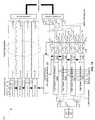
- FIG. 1Ais a block diagram of a photonically enabled CMOS chip, in accordance with an embodiment of the invention.
- FIG. 1Bis diagram illustrating an exemplary CMOS chip, in accordance with an embodiment of the invention.
- FIG. 1Cis a diagram illustrating an exemplary CMOS chip coupled to an optical fiber cable, in accordance with an embodiment of the invention.
- FIG. 2is a block diagram illustrating an exemplary narrowband receiver architecture, in accordance with an embodiment of the invention.
- FIG. 3is a block diagram of an exemplary narrow-band, non-linear optoelectronic receiver system, in accordance with an embodiment of the invention.
- FIG. 4is a plot of an input signal and the resulting output signal, in accordance with an embodiment of the invention.
- FIG. 5is a diagram illustrating performance improvements versus filter and noise bandwidth, in accordance with an embodiment of the invention.
- FIG. 6is a diagram illustrating sensitivity penalty at a bit error rate (BER) of 1e-12, in accordance with an embodiment of the invention.
- FIG. 7is a diagram illustrating input and output signals in a narrow-band, non-linear optoelectronic receiver, in accordance with an embodiment of the invention.
- FIG. 8is a flow diagram illustrating exemplary steps for a narrow-band, non-linear optoelectronic receiver, in accordance with an embodiment of the invention.
- Certain aspects of the inventionmay be found in a method and system for a narrowband, non-linear optoelectronic receiver.
- Exemplary aspects of the inventionmay comprise amplifying a received signal, limiting a bandwidth of the received signal, and restoring the amplified, bandwidth-limited received signal utilizing a level restorer.
- the level restorermay comprise a non-return to zero (NRZ) level restorer.
- the NRZ level restorermay comprise a pulse-triggered bistable circuit.
- the pulse-triggered bistable circuitmay comprise two parallel inverters, where a first of the inverters comprises a feedback path for a second of the inverters, and where the inverters may comprise single-ended or differential inverters.
- a photogenerated signalmay be amplified in the receiver utilizing a transimpedance amplifier and one or more variable gain amplifiers (VGAs).
- VGAsvariable gain amplifiers
- a received electrical signalmay be amplified via one or more VGAs.
- the bandwidth of the received signalmay be limited utilizing one or more of a low pass filter, a bandpass filter, a high pass filter, a differentiator, and/or a series capacitance on the chip.
- the signalmay be received from a photodiode integrated on the chip.
- FIG. 1Ais a block diagram of a photonically enabled CMOS chip, in accordance with an embodiment of the invention.
- optoelectronic devices on a CMOS chip 130comprising high speed optical modulators 105 A- 105 D, high-speed photodiodes 111 A- 111 D, monitor photodiodes 113 A- 113 H, and optical devices comprising taps 103 A- 103 K, optical terminations 115 A- 115 D, and grating couplers 117 A- 117 H.
- TIA/LAstransimpedance and limiting amplifiers
- Optical signalsare communicated between optical and optoelectronic devices via optical waveguides fabricated in the CMOS chip 130 .
- the high speed optical modulators 105 A- 105 Dcomprise Mach-Zehnder or ring modulators, for example, and enable the modulation of the CW laser input signal.
- the high speed optical modulators 105 A- 105 Dare controlled by the control sections 112 A- 112 D, and the outputs of the modulators are optically coupled via waveguides to the grating couplers 117 E- 117 H.
- the taps 103 D- 103 Kcomprise four-port optical couplers, for example, and are utilized to sample the optical signals generated by the high speed optical modulators 105 A- 105 D, with the sampled signals being measured by the monitor photodiodes 113 A- 113 H.
- the unused branches of the taps 103 D- 103 Kare terminated by optical terminations 115 A- 115 D to avoid back reflections of unwanted signals.
- the grating couplers 117 A- 117 Hcomprise optical gratings that enable coupling of light into and out of the CMOS chip 130 .
- the grating couplers 117 A- 117 Dare utilized to couple light received from optical fibers into the CMOS chip 130
- the grating couplers 117 E- 117 Hare utilized to couple light from the CMOS chip 130 into optical fibers.
- the optical fibersmay be epoxied, for example, to the CMOS chip, and may be aligned at an angle from normal to the surface of the CMOS chip 130 to optimize coupling efficiency.
- the high-speed photodiodes 111 A- 111 Dconvert optical signals received from the grating couplers 117 A- 117 D into electrical signals that are communicated to the TIA/LAs 107 A- 107 D for processing.
- the analog and digital control circuits 109may control gain levels or other parameters in the operation of the TIA/LAs 107 A- 107 D.
- the TIA/LAs 107 A- 107 Dthen communicate electrical signals to other circuitry on the CMOS chip 130 and/or circuitry/devices off-chip.
- the TIA/Las 107 A- 107 Dmay comprise narrowband, non-linear optoelectronic receiver circuitry. Accordingly, the narrowband receiver front-end may be followed by a non-return to zero (NRZ) level restorer circuit. This circuit limits the bandwidth of the optical receiver in order to decrease the integrated noise, thereby increasing the signal to noise ratio. An NRZ level restorer may be used to convert the resulting data pulses back into NRZ data.
- NRZnon-return to zero
- the narrowband receiver front-endprovides amplification in a narrow band which includes the maximum data tone (i.e. 5 GHz for 10 Gb/s NRZ data).
- This limited bandwidthmay be implemented in a variety of ways including, but not limited to, the integration of a series filter, such as high pass, band pass or differentiating filters, for example.
- a non-linear NRZ level restorermay then be used to convert the resulting pulses back to their NRZ levels, creating an effectively 0 Hz low frequency cut-off.
- the NRZ level restorermay be implemented using a variety of techniques, including a bistable cross-coupled inverter pair, which may be pulse triggered to switch between its two states.
- the control sections 112 A- 112 Dcomprise electronic circuitry that enable modulation of the CW laser signal received from the taps 103 A- 103 C.
- the high speed optical modulators 105 A- 105 Drequire high-speed electrical signals to modulate the refractive index in respective branches of a Mach-Zehnder interferometer (MZI), for example.
- MZIMach-Zehnder interferometer
- the voltage swing required for driving the MZIis a significant power drain in the CMOS chip 130 . Thus, if the electrical signal for driving the modulator may be split into domains with each domain traversing a lower voltage swing, power efficiency is increased.
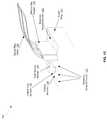
- FIG. 1Bis a diagram illustrating an exemplary CMOS chip, in accordance with an embodiment of the invention.
- the CMOS chip 130comprising electronic devices/circuits 131 , optical and optoelectronic devices 133 , a light source interface 135 , CMOS chip surface 137 , an optical fiber interface 139 , and CMOS guard ring 141 .
- the light source interface 135 and the optical fiber interface 139comprise grating couplers that enable coupling of light signals via the CMOS chip surface 137 , as opposed to the edges of the chip as with conventional edge-emitting devices. Coupling light signals via the CMOS chip surface 137 enables the use of the CMOS guard ring 141 which protects the chip mechanically and prevents the entry of contaminants via the chip edge.
- the electronic devices/circuits 131comprise circuitry such as the TIA/LAs 107 A- 107 D and the analog and digital control circuits 109 described with respect to FIG. 1A , for example.
- the optical and optoelectronic devices 133comprise devices such as the taps 103 A- 103 K, optical terminations 115 A- 115 D, grating couplers 117 A- 117 H, high speed optical modulators 105 A- 105 D, high-speed photodiodes 111 A- 111 D, and monitor photodiodes 113 A- 113 H.
- FIG. 1Cis a diagram illustrating an exemplary CMOS chip coupled to an optical fiber cable, in accordance with an embodiment of the invention.
- the CMOS chip 130comprising the electronic devices/circuits 131 , the optical and optoelectronic devices 133 , the light source interface 135 , the CMOS chip surface 137 , and the CMOS guard ring 141 .
- a fiber to chip coupler 143there is also shown a fiber to chip coupler 143 , an optical fiber cable 145 , and a light source module 147 .
- the CMOS chip 130comprising the electronic devices/circuits 131 , the optical and optoelectronic devices 133 , the light source interface 135 , the CMOS chip surface 137 , and the CMOS guard ring 141 may be as described with respect to FIG. 1B .
- the optical fiber cablemay be affixed, via epoxy for example, to the CMOS chip surface 137 .
- the fiber chip coupler 143enables the physical coupling of the optical fiber cable 145 to the CMOS chip 130 .
- the light source module 147may be affixed, via epoxy or solder, for example, to the CMOS chip surface 137 . In this manner a high power light source may be integrated with optoelectronic and electronic functionalities of one or more high-speed optoelectronic transceivers on a single CMOS chip.
- FIG. 2is a block diagram illustrating an exemplary narrowband receiver architecture, in accordance with an embodiment of the invention.
- a receiver architecture 200comprising a filter 201 and a non-return to zero (NRZ) bistable level restorer 203 .
- an input signal 205There is also shown an input signal 205 , a filtered signal 207 , and an output signal 209 .
- NRZnon-return to zero
- the filter 201comprises circuitry for filtering signals of frequencies outside of a desired frequency band.
- the filtermay allow signals above a frequency, f f , and attenuate signals below f f , as shown in the frequency response plot shown below the filtered signal 207 .
- the filter 201may limit the bandwidth of the optical receiver in order to decrease the integrated noise, thereby increasing the signal to noise ratio.
- the NRZ bistable level restorer 203may convert the resulting data pulses back into NRZ data.
- the NRZ bistable level restorer 203may be implemented using a variety of embodiments including a bistable cross-coupled inverter pair, for example, which may be pulse triggered to switch between its two states.
- the NRZ level restorer 203may comprise a pulse-triggered bistable circuit, a Schmitt-trigger circuit, an RS flip-flop with an inverter on the R input, or a cross-coupled transistor pair, for example.
- the bistable circuitmay comprise an inverter with a second inverter as feedback from the output to the input, where the inverters may be single-ended or differential.
- the narrowband receiver architecture 200may provide amplification in a narrow band which includes the maximum data tone (i.e. 5 GHz for a 10 Gb/s NRZ data). This limited bandwidth may be implemented in a variety of ways including, but not limited to, the integration of a series filter, such as a high pass, band pass, and/or differentiating filter.
- the NRZ bistable level restorer 203may then convert the resulting pulses back to their NRZ levels, creating an effectively 0 Hz low frequency cut-off.
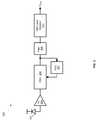
- FIG. 3is a block diagram of an exemplary narrow-band, non-linear optoelectronic receiver system, in accordance with an embodiment of the invention.
- a receiver 300comprising a photodetector 301 , a transimpedance amplifier (TIA) 303 , a variable gain amplifier (VGA) 305 , an automatic gain control (AGC) block 307 , a filter 309 , and an NRZ level restorer 311 .
- TIAtransimpedance amplifier
- VGAvariable gain amplifier
- AGCautomatic gain control
- the TIA 303comprises an amplifier that is enabled to receive an input current signal and generate a voltage output signal.
- the photodetector 301comprises a germanium diode, for example, and may be integrated on the same chip as the TIA 303 , the VGA 305 , the AGC 307 , the filter 309 , and the NRZ level restorer 311 .
- the VGA 305comprises an amplifier that may be enabled to receive an input signal and generate an amplified output signal, where the gain level may be configured depending on the desired signal level.
- the VGA 305may also receive as an input, an output signal from the AGC 307 , which may enable the control of the gain level of the VGA 305 .
- the AGC block 307may determine the signal level at the output of the VGA 305 , compare to the desired level, and generate an output signal to adjust the gain of the VGA 305 accordingly.
- the filter 309comprises a high pass filter to remove unwanted signals below a cutoff frequency, such as the cutoff frequency f f , shown in FIG. 2 . In this manner, the desired signal may be in the frequency range allowed to pass, while the low frequency noise signal may be filtered out.
- the filter 309may comprise a high-pass filter, a band-pass filter, a differentiator, or a series capacitance, for example. Additionally, the filter 309 may be placed at any point in the circuit from before the TIA 303 to after the last amplifier stage, as long as it precedes the NRZ level restorer 311 .
- the NRZ level restorer 311may be substantially similar to the NRZ bistable level restorer 203 , described with respect to FIG. 2 , and may be enabled to receive the filtered signal from the filter 309 , and generate an output signal V OUT , with a restored waveform, as shown by the output signal 209 in FIG. 2 .
- an optical signalmay be received by the photodetector 301 and converted into an electrical current, which may be converted to a voltage signal by the TIA 303 .
- the resulting signalmay then be amplified by the VGA 305 at a gain level configured by the AGC 307 .
- the AGC 307may determine the signal level at the output of the VGA 305 and adjust the gain of the VGA 305 as needed.
- the filter 309may filter out low frequencies in the amplified signal with the resulting signal being communicated to the NRZ level restorer 311 .
- the NRZ level restorermay restore the received signal to a square wave signal, resulting in the output signal V OUT .
- the limited receiver linear bandwidthdecreases the integrated receiver noise, improving the signal to noise ratio and hence the sensitivity of the receiver, relative to a traditional receiver without the filtering and NRZ level restorer.
- the limited bandwidthalso decreases susceptibility to crosstalk and power supply noise which is outside the signal bandwidth.
- the non-linear NRZ level restorerallows higher low-frequency cut-offs to be used throughout the receiver, including the AGC, offset compensation and TIA. In this way, the chip area is decreased due to higher AGC and offset compensation circuit cut-off frequencies, the off-chip capacitors are not required for compensation circuits, simplifying multi-channel scaling, coding requirements are removed for external data, and it allows an AC coupled differential input to be used.
- the inventionis not limited to optoelectronic applications. Accordingly, in instances where the Rx 300 may be utilized for electrical communication as opposed to optical communication, the TIA 303 may be eliminated or replaced with one or more voltage domain amplifiers.
- FIG. 4is a plot of an input signal and the resulting output signal, in accordance with an embodiment of the invention.
- the input signal 401comprising 10 Gbps NRZ data with an approximately 159 MHz sinusoidal interferer.
- the output signal 403is the simulated output signal of the optoelectronic receiver 300 , demonstrating the large reduction of noise utilizing the filter and NRZ level restorer.
- FIG. 5is a diagram illustrating performance improvements versus filter and noise frequency, in accordance with an embodiment of the invention.
- a sensitivity improvement plot 510and a decision threshold plot 503 .
- the x-axis for both plotsis the ratio, B, of the filter frequency f f , to the noise corner frequency f n .
- the sensitivity improvement plot 501demonstrates the improvement in sensitivity when the filter frequency approaches that of the noise frequency, narrowing the bandwidth of the allowed signal.
- the increase in the normalized decision threshold with Bthe magnitude of the input signal required to switch from low to high increases as the bandwidth narrows, thus demonstrating the tradeoff involved in determining the filter cutoff frequency.
- FIG. 6is a diagram illustrating sensitivity penalty at a bit error rate (BER) of 1e-12, in accordance with an embodiment of the invention.
- BERbit error rate
- FIG. 6there is shown a sensitivity penalty versus DC balance plot 601 and a sensitivity penalty versus ‘0/1’ noise ratio plot 603 . Due to the DFE-type behavior of this circuit, a single bit flip will result in errors until another bit flip occurs. For completely random data with equal probabilities of zeros and ones and errors that are uniformly distributed in time, the increase in average BER due to error clustering is 50%, assuming run lengths from 1 to infinity are allowed. The plots in FIG. 6 , show that the sensitivity penalty is less than ⁇ 0.1 dB under practical conditions.
- FIG. 7is a diagram illustrating input and output signals in a narrow-band, non-linear optoelectronic receiver, in accordance with an embodiment of the invention.
- an input signal 701there is shown an input signal 701 , a simulated VGA output signal 703 , and a simulated NRZ level restorer output 705 versus time.
- the exemplary input signal 701illustrates a square wave signal, and the distorted signal resulting after the VGA 305 , due to non-zero low frequency cut-off, is illustrated by the VGA output signal 703 . Because the circuit is effectively AC coupled to the rest of the system and its feedback maintains the last valid bit, the effective low frequency cut-off is OHz. Long runs of zeros or ones will not produce any pulses and will cause the VGA output 703 to squelch, but it will not flip the state of the Circuit output until there is another pulse edge to flip the state of the circuit.
- FIG. 8is a flow diagram illustrating exemplary steps for a narrow-band, non-linear optoelectronic receiver, in accordance with an embodiment of the invention.
- step 803after start step 801 , an optical signal is received by a photodetector 301 resulting in a photogenerated current.
- the TIA 303converts the current to a voltage signal that is amplified in step 807 by the VGA 305 with the gain level controlled by the AGC 307 .
- the amplified signalis filtered by the filter 309 and then restored by the NRZ level restorer 311 , followed by end step 811 .
- a method and systemare disclosed for amplifying a received signal, limiting a bandwidth of the received signal, and restoring the amplified, bandwidth-limited received signal utilizing a level restorer 203 / 311 .
- the level restorermay comprise a non-return to zero (NRZ) level restorer 203 / 311 .
- the NRZ level restorer 203may comprise a pulse-triggered bistable circuit.
- the pulse-triggered bistable circuit 203may comprise two parallel inverters, and wherein a first of the inverters comprises a feedback path for a second of the inverters, which may comprise single-ended or differential inverters.
- a photogenerated signalmay be amplified in the receiver 300 utilizing a transimpedance amplifier 303 and one or more variable gain amplifiers (VGAs) 305 .
- a received electrical signalmay be amplified via one or more VGAs 305 .
- the bandwidth of the received signalmay be limited utilizing one or more of: a low pass filter, a bandpass filter, a high pass filter 201 , a differentiator, or a series capacitance on the chip.
- the signalmay be received from a photodiode 301 integrated on the chip 130 .
Landscapes
- Physics & Mathematics (AREA)
- Electromagnetism (AREA)
- Engineering & Computer Science (AREA)
- Computer Networks & Wireless Communication (AREA)
- Signal Processing (AREA)
- Optical Communication System (AREA)
- Amplifiers (AREA)
Abstract
Description
Claims (14)
Priority Applications (4)
| Application Number | Priority Date | Filing Date | Title |
|---|---|---|---|
| US12/245,867US8787774B2 (en) | 2007-10-10 | 2008-10-06 | Method and system for a narrowband, non-linear optoelectronic receiver |
| US14/337,736US9209907B2 (en) | 2007-10-10 | 2014-07-22 | Method and system for a narrowband, non-linear optoelectronic receiver |
| US14/957,083US9819422B2 (en) | 2007-10-10 | 2015-12-02 | Method and system for a narrowband, non-linear optoelectronic receiver |
| US15/797,664US10608750B2 (en) | 2007-10-10 | 2017-10-30 | Method and system for a narrowband, non-linear optoelectronic receiver |
Applications Claiming Priority (2)
| Application Number | Priority Date | Filing Date | Title |
|---|---|---|---|
| US99831407P | 2007-10-10 | 2007-10-10 | |
| US12/245,867US8787774B2 (en) | 2007-10-10 | 2008-10-06 | Method and system for a narrowband, non-linear optoelectronic receiver |
Related Child Applications (1)
| Application Number | Title | Priority Date | Filing Date |
|---|---|---|---|
| US14/337,736ContinuationUS9209907B2 (en) | 2007-10-10 | 2014-07-22 | Method and system for a narrowband, non-linear optoelectronic receiver |
Publications (2)
| Publication Number | Publication Date |
|---|---|
| US20090097865A1 US20090097865A1 (en) | 2009-04-16 |
| US8787774B2true US8787774B2 (en) | 2014-07-22 |
Family
ID=40534330
Family Applications (4)
| Application Number | Title | Priority Date | Filing Date |
|---|---|---|---|
| US12/245,867Active2032-12-02US8787774B2 (en) | 2007-10-10 | 2008-10-06 | Method and system for a narrowband, non-linear optoelectronic receiver |
| US14/337,736ActiveUS9209907B2 (en) | 2007-10-10 | 2014-07-22 | Method and system for a narrowband, non-linear optoelectronic receiver |
| US14/957,083ActiveUS9819422B2 (en) | 2007-10-10 | 2015-12-02 | Method and system for a narrowband, non-linear optoelectronic receiver |
| US15/797,664ActiveUS10608750B2 (en) | 2007-10-10 | 2017-10-30 | Method and system for a narrowband, non-linear optoelectronic receiver |
Family Applications After (3)
| Application Number | Title | Priority Date | Filing Date |
|---|---|---|---|
| US14/337,736ActiveUS9209907B2 (en) | 2007-10-10 | 2014-07-22 | Method and system for a narrowband, non-linear optoelectronic receiver |
| US14/957,083ActiveUS9819422B2 (en) | 2007-10-10 | 2015-12-02 | Method and system for a narrowband, non-linear optoelectronic receiver |
| US15/797,664ActiveUS10608750B2 (en) | 2007-10-10 | 2017-10-30 | Method and system for a narrowband, non-linear optoelectronic receiver |
Country Status (1)
| Country | Link |
|---|---|
| US (4) | US8787774B2 (en) |
Cited By (10)
| Publication number | Priority date | Publication date | Assignee | Title |
|---|---|---|---|---|
| US20160087728A1 (en)* | 2007-10-10 | 2016-03-24 | Luxtera, Inc. | Method And System For A Narrowband, Non-Linear Optoelectronic Receiver |
| US9667351B2 (en) | 2015-10-30 | 2017-05-30 | Avago Technologies General Ip (Singapore) Pte. Ltd. | Simultaneous bandwidth extension at high gain and peaking reduction at minimum gain for wideband, variable gain, linear optical receivers |
| US9864138B2 (en) | 2015-01-05 | 2018-01-09 | The Research Foundation For The State University Of New York | Integrated photonics including germanium |
| US10698156B2 (en) | 2017-04-27 | 2020-06-30 | The Research Foundation For The State University Of New York | Wafer scale bonded active photonics interposer |
| US10816724B2 (en) | 2018-04-05 | 2020-10-27 | The Research Foundation For The State University Of New York | Fabricating photonics structure light signal transmission regions |
| US10877300B2 (en) | 2018-04-04 | 2020-12-29 | The Research Foundation For The State University Of New York | Heterogeneous structure on an integrated photonics platform |
| US10976491B2 (en) | 2016-11-23 | 2021-04-13 | The Research Foundation For The State University Of New York | Photonics interposer optoelectronics |
| US11029466B2 (en) | 2018-11-21 | 2021-06-08 | The Research Foundation For The State University Of New York | Photonics structure with integrated laser |
| US11550099B2 (en) | 2018-11-21 | 2023-01-10 | The Research Foundation For The State University Of New York | Photonics optoelectrical system |
| US12366705B2 (en) | 2018-11-21 | 2025-07-22 | The Research Foundation For The State Univeristy Of Newyork | Photonics optoelectrical system |
Families Citing this family (8)
| Publication number | Priority date | Publication date | Assignee | Title |
|---|---|---|---|---|
| CN102957477B (en)* | 2011-08-30 | 2015-12-09 | 华为技术有限公司 | Signal detecting method and optical signal reception system |
| WO2017074385A1 (en)* | 2015-10-29 | 2017-05-04 | Hewlett-Packard Enterprise | Receivers with automatic gain control |
| CN107517085A (en)* | 2017-08-11 | 2017-12-26 | 西安科锐盛创新科技有限公司 | an optical receiver |
| US10505509B2 (en) | 2017-10-31 | 2019-12-10 | Cisco Technology, Inc. | Process and temperature insensitive linear circuit |
| US10606004B2 (en)* | 2018-06-01 | 2020-03-31 | Intel Corporation | Distributed optoelectronic receiver |
| CN110896312B (en)* | 2018-09-12 | 2021-10-01 | 瑞昱半导体股份有限公司 | Device and method for executing bandwidth detection |
| US11139799B2 (en)* | 2019-10-18 | 2021-10-05 | Texas Instruments Incorporated | Clock filter with negative resistor circuit |
| US11249499B2 (en) | 2020-03-04 | 2022-02-15 | Cisco Technology, Inc. | Linear transimpedance amplifier dual regulator architecture and tuning |
Citations (23)
| Publication number | Priority date | Publication date | Assignee | Title |
|---|---|---|---|---|
| US3585598A (en)* | 1969-07-24 | 1971-06-15 | Amp Inc | Alphanumeric,variable word length,channel scanning selective signalling system |
| US3980825A (en)* | 1973-02-12 | 1976-09-14 | U.S. Philips Corporation | System for the transmission of split-phase Manchester coded bivalent information signals |
| US4019048A (en)* | 1976-03-22 | 1977-04-19 | Bell Telephone Laboratories, Incorporated | Regenerator for an optical transmission system |
| US4350973A (en)* | 1979-07-23 | 1982-09-21 | Honeywell Information Systems Inc. | Receiver apparatus for converting optically encoded binary data to electrical signals |
| US4479266A (en)* | 1981-08-12 | 1984-10-23 | Thomson-Csf | Multiple-threshold optical receiver for a variable-rate digital data transmission system |
| US4481676A (en)* | 1981-08-21 | 1984-11-06 | Thomson-Csf | Transmitter-receiver system for variable-rate digital data transmission via optical-fiber links |
| US4644145A (en)* | 1984-05-04 | 1987-02-17 | Standard Elektrik Lorenz Aktiengesellschaft | Optical receiver with electrically variable attenuator |
| US4706300A (en)* | 1983-01-31 | 1987-11-10 | Nec Corporation | Optical heterodyne detection pulse receiving system and method |
| US4713841A (en)* | 1985-06-03 | 1987-12-15 | Itt Electro Optical Products, A Division Of Itt Corporation | Synchronous, asynchronous, data rate transparent fiber optic communications link |
| US4980577A (en)* | 1987-06-18 | 1990-12-25 | Advanced Micro Devices, Inc. | Dual triggered edge-sensitive asynchrounous flip-flop |
| US5319438A (en)* | 1992-01-24 | 1994-06-07 | Board Of Regents, The University Of Texas System | Interferometric, self-homodyne optical receiver and method and optical transmission system incorporating same |
| US5337388A (en)* | 1993-08-03 | 1994-08-09 | International Business Machines Corporation | Matrix of pluggable connectors for connecting large numbers of clustered electrical and/or opticcal cables to a module |
| US20020027689A1 (en)* | 2000-09-05 | 2002-03-07 | Meir Bartur | Fiber optic transceiver employing front end level control |
| US20020089728A1 (en)* | 2001-01-05 | 2002-07-11 | Samsung Electronics Co., Ltd. | High speed optical receiver implemented in one chip |
| US20020186048A1 (en)* | 2000-11-13 | 2002-12-12 | Primarion, Inc. | Method and circuit for pre-emphasis equalization in high speed data communications |
| US6642765B2 (en)* | 2001-12-06 | 2003-11-04 | Intel Corporation | Transmission-gate based flip-flop |
| US20060002489A1 (en)* | 2000-11-28 | 2006-01-05 | Muneer Zuhdi | Bidirectional optical communications having quick data recovery without first establishing timing and phase lock |
| US7215891B1 (en)* | 2003-06-06 | 2007-05-08 | Jds Uniphase Corporation | Integrated driving, receiving, controlling, and monitoring for optical transceivers |
| US7259031B1 (en)* | 2004-01-14 | 2007-08-21 | Luxtera, Inc. | Integrated photonic-electronic circuits and systems |
| US7324207B1 (en)* | 2004-04-30 | 2008-01-29 | Translume, Inc. | Optical pulse correlator having an interferometer array |
| US20090196632A1 (en)* | 2008-02-04 | 2009-08-06 | Zhenhong Zhang | Optical burst receiver and method |
| US20100284700A1 (en)* | 2005-02-23 | 2010-11-11 | Kg Technology Associates, Inc. | Optical Fiber Communication Link |
| US8110823B2 (en)* | 2006-01-20 | 2012-02-07 | The Regents Of The University Of California | III-V photonic integration on silicon |
Family Cites Families (22)
| Publication number | Priority date | Publication date | Assignee | Title |
|---|---|---|---|---|
| US4426662A (en)* | 1982-01-18 | 1984-01-17 | Zenith Radio Corporation | IR Remote control detector/decoder |
| US4736391A (en)* | 1986-07-22 | 1988-04-05 | General Electric Company | Threshold control with data receiver |
| JPH0752862B2 (en)* | 1987-10-29 | 1995-06-05 | 日本電気株式会社 | 4-level FSK optical communication system |
| JPH0478235A (en)* | 1990-07-18 | 1992-03-12 | Fujitsu Ltd | Direct modulation PSK transmission system and automatic frequency control method, demodulation method and phase noise suppression method in the system |
| JPH05244094A (en)* | 1992-02-26 | 1993-09-21 | Toshiba Corp | Optical transmission equipment |
| US5373388A (en)* | 1993-02-25 | 1994-12-13 | International Business Machines, Inc. | AC coupled fiber optic receiver with DC coupled characteristics |
| US6118567A (en)* | 1997-09-30 | 2000-09-12 | Motorola, Inc. | Efficient encoding and detection method and device for binary intensity modulated optical data signals |
| US6236317B1 (en)* | 1998-04-29 | 2001-05-22 | Food Safety Solution Corp. | Method and apparatus for monitoring actions taken by a user for enhancing hygiene |
| US6053613A (en)* | 1998-05-15 | 2000-04-25 | Carl Zeiss, Inc. | Optical coherence tomography with new interferometer |
| CA2311434C (en)* | 2000-06-13 | 2004-10-19 | Ibm Canada Limited-Ibm Canada Limitee | Differential photoelectric receiver circuit |
| DE10038616B4 (en)* | 2000-08-08 | 2012-07-12 | Atmel Automotive Gmbh | Method and arrangement for interference suppression in a receiver circuit |
| DE10054529A1 (en)* | 2000-11-03 | 2002-05-29 | Vishay Semiconductor Gmbh | Energy-saving method for the wireless reception of data modulated on a carrier signal |
| EP1494413A1 (en)* | 2003-07-02 | 2005-01-05 | CoreOptics, Inc., c/o The Corporation Trust Center | Channel estimation and sequence estimation for the reception of optical signal |
| KR100566195B1 (en)* | 2003-08-27 | 2006-03-29 | 삼성전자주식회사 | Duobinary Optical Transmitter Using Semiconductor Optical Amplifier |
| US7436911B2 (en)* | 2005-10-11 | 2008-10-14 | L-3 Communications Integrated Systems L.P. | Nyquist folded bandpass sampling receivers with narrow band filters for UWB pulses and related methods |
| JP4654105B2 (en)* | 2005-10-11 | 2011-03-16 | 富士通株式会社 | Optical receiver circuit |
| JP4695500B2 (en)* | 2005-12-02 | 2011-06-08 | 富士通株式会社 | Signal reproducing apparatus, optical receiving apparatus, and signal processing method |
| US7574145B2 (en)* | 2005-12-30 | 2009-08-11 | Intel Corporation | Optical receiver with duo-binary encoder |
| US7668463B2 (en)* | 2006-03-03 | 2010-02-23 | Alcatel-Lucent Usa Inc. | Method and apparatus for generating and transmitting WDM MWOF signals |
| US7498882B2 (en)* | 2006-04-18 | 2009-03-03 | Rambus Inc. | Signaling system with low-power automatic gain control |
| US8787774B2 (en)* | 2007-10-10 | 2014-07-22 | Luxtera, Inc. | Method and system for a narrowband, non-linear optoelectronic receiver |
| DE102008029620A1 (en)* | 2008-06-23 | 2009-12-24 | Vishay Semiconductor Gmbh | Infrared receiver circuit |
- 2008
- 2008-10-06USUS12/245,867patent/US8787774B2/enactiveActive
- 2014
- 2014-07-22USUS14/337,736patent/US9209907B2/enactiveActive
- 2015
- 2015-12-02USUS14/957,083patent/US9819422B2/enactiveActive
- 2017
- 2017-10-30USUS15/797,664patent/US10608750B2/enactiveActive
Patent Citations (23)
| Publication number | Priority date | Publication date | Assignee | Title |
|---|---|---|---|---|
| US3585598A (en)* | 1969-07-24 | 1971-06-15 | Amp Inc | Alphanumeric,variable word length,channel scanning selective signalling system |
| US3980825A (en)* | 1973-02-12 | 1976-09-14 | U.S. Philips Corporation | System for the transmission of split-phase Manchester coded bivalent information signals |
| US4019048A (en)* | 1976-03-22 | 1977-04-19 | Bell Telephone Laboratories, Incorporated | Regenerator for an optical transmission system |
| US4350973A (en)* | 1979-07-23 | 1982-09-21 | Honeywell Information Systems Inc. | Receiver apparatus for converting optically encoded binary data to electrical signals |
| US4479266A (en)* | 1981-08-12 | 1984-10-23 | Thomson-Csf | Multiple-threshold optical receiver for a variable-rate digital data transmission system |
| US4481676A (en)* | 1981-08-21 | 1984-11-06 | Thomson-Csf | Transmitter-receiver system for variable-rate digital data transmission via optical-fiber links |
| US4706300A (en)* | 1983-01-31 | 1987-11-10 | Nec Corporation | Optical heterodyne detection pulse receiving system and method |
| US4644145A (en)* | 1984-05-04 | 1987-02-17 | Standard Elektrik Lorenz Aktiengesellschaft | Optical receiver with electrically variable attenuator |
| US4713841A (en)* | 1985-06-03 | 1987-12-15 | Itt Electro Optical Products, A Division Of Itt Corporation | Synchronous, asynchronous, data rate transparent fiber optic communications link |
| US4980577A (en)* | 1987-06-18 | 1990-12-25 | Advanced Micro Devices, Inc. | Dual triggered edge-sensitive asynchrounous flip-flop |
| US5319438A (en)* | 1992-01-24 | 1994-06-07 | Board Of Regents, The University Of Texas System | Interferometric, self-homodyne optical receiver and method and optical transmission system incorporating same |
| US5337388A (en)* | 1993-08-03 | 1994-08-09 | International Business Machines Corporation | Matrix of pluggable connectors for connecting large numbers of clustered electrical and/or opticcal cables to a module |
| US20020027689A1 (en)* | 2000-09-05 | 2002-03-07 | Meir Bartur | Fiber optic transceiver employing front end level control |
| US20020186048A1 (en)* | 2000-11-13 | 2002-12-12 | Primarion, Inc. | Method and circuit for pre-emphasis equalization in high speed data communications |
| US20060002489A1 (en)* | 2000-11-28 | 2006-01-05 | Muneer Zuhdi | Bidirectional optical communications having quick data recovery without first establishing timing and phase lock |
| US20020089728A1 (en)* | 2001-01-05 | 2002-07-11 | Samsung Electronics Co., Ltd. | High speed optical receiver implemented in one chip |
| US6642765B2 (en)* | 2001-12-06 | 2003-11-04 | Intel Corporation | Transmission-gate based flip-flop |
| US7215891B1 (en)* | 2003-06-06 | 2007-05-08 | Jds Uniphase Corporation | Integrated driving, receiving, controlling, and monitoring for optical transceivers |
| US7259031B1 (en)* | 2004-01-14 | 2007-08-21 | Luxtera, Inc. | Integrated photonic-electronic circuits and systems |
| US7324207B1 (en)* | 2004-04-30 | 2008-01-29 | Translume, Inc. | Optical pulse correlator having an interferometer array |
| US20100284700A1 (en)* | 2005-02-23 | 2010-11-11 | Kg Technology Associates, Inc. | Optical Fiber Communication Link |
| US8110823B2 (en)* | 2006-01-20 | 2012-02-07 | The Regents Of The University Of California | III-V photonic integration on silicon |
| US20090196632A1 (en)* | 2008-02-04 | 2009-08-06 | Zhenhong Zhang | Optical burst receiver and method |
Non-Patent Citations (5)
| Title |
|---|
| "2005 IEEE International SOI Conference, CMOS Photonics(TM)-SOI Learns a New Trick Cary Gunn, PhD".* |
| "2005 IEEE International SOI Conference, CMOS Photonics™—SOI Learns a New Trick Cary Gunn, PhD".* |
| A 2.5-mW SOS CMOS Optical Receiver for Chip-to-Chip Interconnect Alyssa Apsel, Member, IEEE, Zhongtao Fu, Member, IEEE, and Andreas G. Andreou, Member, IEEE Journal of Lightwave Technology, vol. 22, No. 9, Sep. 2004.* |
| Fast Offset Compensation for a 10Gbps Limit Amplifier by Ethan A. Crain Massachusetts Institute of Technology, Dec. 1995 Submitted to the Department of Electrical Engineering and Computer Science May 2004.* |
| Silicon Photonics Bahram Jalali, Fellow, IEEE, and Sasan Fathpour, Member, IEEE; Journal of Lightwave Technology, vol. 24, No. 12, Dec. 2006.* |
Cited By (20)
| Publication number | Priority date | Publication date | Assignee | Title |
|---|---|---|---|---|
| US9819422B2 (en)* | 2007-10-10 | 2017-11-14 | Luxtera, Inc. | Method and system for a narrowband, non-linear optoelectronic receiver |
| US20160087728A1 (en)* | 2007-10-10 | 2016-03-24 | Luxtera, Inc. | Method And System For A Narrowband, Non-Linear Optoelectronic Receiver |
| US10830952B2 (en) | 2015-01-05 | 2020-11-10 | The Research Foundation For The State University Of New York | Integrated photonics including germanium |
| US9864138B2 (en) | 2015-01-05 | 2018-01-09 | The Research Foundation For The State University Of New York | Integrated photonics including germanium |
| US10295745B2 (en) | 2015-01-05 | 2019-05-21 | The Research Foundation For The State University Of New York | Integrated photonics including germanium |
| US10571631B2 (en) | 2015-01-05 | 2020-02-25 | The Research Foundation For The State University Of New York | Integrated photonics including waveguiding material |
| US11703643B2 (en) | 2015-01-05 | 2023-07-18 | The Research Foundation For The State University Of New York | Integrated photonics including waveguiding material |
| US9667351B2 (en) | 2015-10-30 | 2017-05-30 | Avago Technologies General Ip (Singapore) Pte. Ltd. | Simultaneous bandwidth extension at high gain and peaking reduction at minimum gain for wideband, variable gain, linear optical receivers |
| US10976491B2 (en) | 2016-11-23 | 2021-04-13 | The Research Foundation For The State University Of New York | Photonics interposer optoelectronics |
| US11435523B2 (en) | 2017-04-27 | 2022-09-06 | The Research Foundation For The State University Of New York | Wafer scale bonded active photonics interposer |
| US10698156B2 (en) | 2017-04-27 | 2020-06-30 | The Research Foundation For The State University Of New York | Wafer scale bonded active photonics interposer |
| US11841531B2 (en) | 2017-04-27 | 2023-12-12 | The Research Foundation For The State University Of New York | Wafer scale bonded active photonics interposer |
| US10877300B2 (en) | 2018-04-04 | 2020-12-29 | The Research Foundation For The State University Of New York | Heterogeneous structure on an integrated photonics platform |
| US11550173B2 (en) | 2018-04-04 | 2023-01-10 | The Research Foundation For The State University Of New York | Heterogeneous structure on an integrated photonics platform |
| US10816724B2 (en) | 2018-04-05 | 2020-10-27 | The Research Foundation For The State University Of New York | Fabricating photonics structure light signal transmission regions |
| US11378739B2 (en) | 2018-04-05 | 2022-07-05 | The Research Foundation For The State University Of New York | Fabricating photonics structure light signal transmission regions |
| US11635568B2 (en) | 2018-04-05 | 2023-04-25 | The Research Foundation For The State University Of New York | Photonics light signal transmission |
| US11029466B2 (en) | 2018-11-21 | 2021-06-08 | The Research Foundation For The State University Of New York | Photonics structure with integrated laser |
| US11550099B2 (en) | 2018-11-21 | 2023-01-10 | The Research Foundation For The State University Of New York | Photonics optoelectrical system |
| US12366705B2 (en) | 2018-11-21 | 2025-07-22 | The Research Foundation For The State Univeristy Of Newyork | Photonics optoelectrical system |
Also Published As
| Publication number | Publication date |
|---|---|
| US20140334832A1 (en) | 2014-11-13 |
| US9209907B2 (en) | 2015-12-08 |
| US20090097865A1 (en) | 2009-04-16 |
| US20180062763A1 (en) | 2018-03-01 |
| US10608750B2 (en) | 2020-03-31 |
| US9819422B2 (en) | 2017-11-14 |
| US20160087728A1 (en) | 2016-03-24 |
Similar Documents
| Publication | Publication Date | Title |
|---|---|---|
| US10608750B2 (en) | Method and system for a narrowband, non-linear optoelectronic receiver | |
| US10623109B2 (en) | Method and system for a distributed optoelectronic receiver | |
| US11418160B2 (en) | Method and system for a feedback transimpedance amplifier with sub-40khz low-frequency cutoff | |
| KR101725878B1 (en) | Integrated circuits in optical receivers | |
| US8604866B2 (en) | Method and system for bandwidth enhancement using hybrid inductors | |
| CN101958750A (en) | An all-optical signal quality monitor based on optical parametric amplifier | |
| Dupuis et al. | 30-Gb/s optical link combining heterogeneously integrated III–V/Si photonics with 32-nm CMOS circuits | |
| US20190109649A1 (en) | Split optical front end receivers | |
| JP2000269892A (en) | Optical receiver with waveform equalization function and method for controlling equalization of optical reception | |
| JP2011004368A (en) | Optical receiver | |
| JP4069036B2 (en) | Mark rate evaluation system | |
| JP7493992B2 (en) | Optical receiving device | |
| CN118316536A (en) | Receiver structure of integrated burst mode optical receiver based on CMOS technology | |
| Vokić et al. | 3D-Integrated Transceiver for Optical Communications | |
| Yoshida et al. | First single-fibre bi-directional XFP transceiver for optical metro/access networks | |
| WO2016006047A1 (en) | Optical reception module | |
| Cheng et al. | An optical receiver circuit for on‐line fiber‐optic characteristics monitoring | |
| Atef et al. | Equalizer Implementations for SI-POF | |
| KR20000053309A (en) | Method and device for signal repetition |
Legal Events
| Date | Code | Title | Description |
|---|---|---|---|
| AS | Assignment | Owner name:SILICON VALLEY BANK,CALIFORNIA Free format text:SECURITY AGREEMENT;ASSIGNOR:LUXTERA, INC.;REEL/FRAME:024091/0191 Effective date:20100317 Owner name:SILICON VALLEY BANK, CALIFORNIA Free format text:SECURITY AGREEMENT;ASSIGNOR:LUXTERA, INC.;REEL/FRAME:024091/0191 Effective date:20100317 | |
| AS | Assignment | Owner name:LUXTERA INC., CALIFORNIA Free format text:ASSIGNMENT OF ASSIGNORS INTEREST;ASSIGNOR:GUCKENBERGER, JOHN ANDREW;REEL/FRAME:028026/0351 Effective date:20081002 | |
| STCF | Information on status: patent grant | Free format text:PATENTED CASE | |
| AS | Assignment | Owner name:SILICON VALLEY BANK, COLORADO Free format text:SECURITY INTEREST;ASSIGNOR:LUXTERA, INC.;REEL/FRAME:042109/0140 Effective date:20170328 | |
| MAFP | Maintenance fee payment | Free format text:PAYMENT OF MAINTENANCE FEE, 4TH YR, SMALL ENTITY (ORIGINAL EVENT CODE: M2551) Year of fee payment:4 | |
| AS | Assignment | Owner name:LUXTERA LLC, DELAWARE Free format text:CHANGE OF NAME;ASSIGNOR:LUXTERA, INC.;REEL/FRAME:052019/0811 Effective date:20190208 | |
| AS | Assignment | Owner name:LUXTERA, LLC, CALIFORNIA Free format text:RELEASE BY SECURED PARTY;ASSIGNOR:SILICON VALLEY BANK;REEL/FRAME:054855/0838 Effective date:20201223 | |
| FEPP | Fee payment procedure | Free format text:ENTITY STATUS SET TO UNDISCOUNTED (ORIGINAL EVENT CODE: BIG.); ENTITY STATUS OF PATENT OWNER: LARGE ENTITY | |
| MAFP | Maintenance fee payment | Free format text:PAYMENT OF MAINTENANCE FEE, 8TH YEAR, LARGE ENTITY (ORIGINAL EVENT CODE: M1552); ENTITY STATUS OF PATENT OWNER: LARGE ENTITY Year of fee payment:8 | |
| AS | Assignment | Owner name:CISCO TECHNOLOGY, INC., CALIFORNIA Free format text:ASSIGNMENT OF ASSIGNORS INTEREST;ASSIGNOR:CISCO SYSTEMS, INC.;REEL/FRAME:058979/0027 Effective date:20220207 | |
| AS | Assignment | Owner name:CISCO TECHNOLOGY, INC., CALIFORNIA Free format text:CORRECTIVE ASSIGNMENT TO CORRECT THE THE ASSIGNOR'S NAME PREVIOUSLY RECORDED AT REEL: 058979 FRAME: 0027. ASSIGNOR(S) HEREBY CONFIRMS THE ASSIGNMENT;ASSIGNOR:LUXTERA LLC;REEL/FRAME:059496/0803 Effective date:20220207 |