US8787502B2 - Capacitive isolated voltage domains - Google Patents
Capacitive isolated voltage domainsDownload PDFInfo
- Publication number
- US8787502B2 US8787502B2US13/454,739US201213454739AUS8787502B2US 8787502 B2US8787502 B2US 8787502B2US 201213454739 AUS201213454739 AUS 201213454739AUS 8787502 B2US8787502 B2US 8787502B2
- Authority
- US
- United States
- Prior art keywords
- signal
- conductor
- conductors
- circuit
- signals
- Prior art date
- Legal status (The legal status is an assumption and is not a legal conclusion. Google has not performed a legal analysis and makes no representation as to the accuracy of the status listed.)
- Active, expires
Links
Images


Classifications
- H—ELECTRICITY
- H03—ELECTRONIC CIRCUITRY
- H03M—CODING; DECODING; CODE CONVERSION IN GENERAL
- H03M5/00—Conversion of the form of the representation of individual digits
- H03M5/02—Conversion to or from representation by pulses
- H03M5/04—Conversion to or from representation by pulses the pulses having two levels
- H03M5/06—Code representation, e.g. transition, for a given bit cell depending only on the information in that bit cell
- H03M5/08—Code representation by pulse width
- H—ELECTRICITY
- H04—ELECTRIC COMMUNICATION TECHNIQUE
- H04B—TRANSMISSION
- H04B5/00—Near-field transmission systems, e.g. inductive or capacitive transmission systems
- H04B5/20—Near-field transmission systems, e.g. inductive or capacitive transmission systems characterised by the transmission technique; characterised by the transmission medium
- H04B5/22—Capacitive coupling
- H—ELECTRICITY
- H04—ELECTRIC COMMUNICATION TECHNIQUE
- H04L—TRANSMISSION OF DIGITAL INFORMATION, e.g. TELEGRAPHIC COMMUNICATION
- H04L25/00—Baseband systems
- H04L25/02—Details ; arrangements for supplying electrical power along data transmission lines
- H04L25/0264—Arrangements for coupling to transmission lines
- H04L25/0266—Arrangements for providing Galvanic isolation, e.g. by means of magnetic or capacitive coupling
- H—ELECTRICITY
- H04—ELECTRIC COMMUNICATION TECHNIQUE
- H04B—TRANSMISSION
- H04B14/00—Transmission systems not characterised by the medium used for transmission
- H04B14/02—Transmission systems not characterised by the medium used for transmission characterised by the use of pulse modulation
- H04B14/026—Transmission systems not characterised by the medium used for transmission characterised by the use of pulse modulation using pulse time characteristics modulation, e.g. width, position, interval
Definitions
- aspects of the present disclosurerelate to apparatuses, devices and methods involving communication interfaces useful for galvanic isolation in circuits.
- Galvanic isolationhas been used for a variety of different applications. For instance, galvanic isolation can be provided between multiple integrated circuit chips, which can be located within the same package or in different packages. Signals can be passed between the integrated circuits using galvanic isolation techniques.
- galvanic isolation techniquesOne type of galvanic isolation technique involves the use of differential signaling and capacitive coupling. These and other galvanic isolation techniques have various undesirable tradeoffs in properties such as, but not necessarily limited to, signal propagation delays, power consumption, pulse width distortion and carrier frequency requirements.
- Differential signaling solutionsuse two separate wires upon which corresponding signals are then transmitted differentially.
- the differentially transmitted signalscan be modulated in a number of different manners in order to convey data.
- a few non-limiting examplesinclude, frequency modulation, amplitude modulation and on-off keying.
- Differential signaling solutionsuse a receiver that uses a direct comparison between the signal levels for each of the two transmitted signals. This direct comparison between two differentially transmitted signals is useful, but also carries some disadvantages.
- aspects of the present disclosurerelate generally to methods, circuits, and devices for communication of data between galvanically isolated circuits.
- a method of communicating data values over a three conductor interfaceis provided. Different data values are transmitted by generating and transmitting three respective signals to a receiver using three respective conductors.
- the first signalis maintained as a set voltage level.
- the second signalis alternated between a high voltage and a low voltage according to a carrier frequency.
- the third signalis alternated between the high and low voltages and is out of phased with the second signal.
- To transmit a first data valuethe first signal is generated on a first conductor, the second signal is generated on a second conductor, and the third signal is generated on a third conductor.
- To transmit a second data valuethe second signal is generated on the first conductor, the first signal is generated on the second conductor, and the third signal is generated on the third conductor.
- a transmitter circuitis included that is configured to generate and transmit the three respective signals described above to a receiver over a three conductor interface.
- the transmitterIn response to a first input data value, the transmitter generates the first signal on a first conductor, the second signal on a second conductor, and the third signal on a third conductor.
- the transmitterIn response to a second input data value, the transmitter generates the second signal on the first conductor, the first signal on the second conductor, and the third signal on the third conductor.
- a receiver circuitis included that is configured to receive the three signals, which are unreferenced to each other, reference the signals to each other, and decode the arrangement of the received signals and conductors to decode the transmitted data value.
- the receiver circuitincludes a reference circuit configured to reference the signals to each other and provide the referenced signals to first and second comparison circuits.
- the first comparison circuitis configured to compare the referenced first signal to a combination of the second and third referenced signals.
- the second comparison circuitis configured to compare the referenced third signal to a combination of the first and second referenced signals.
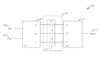
- FIG. 1depicts a block diagram of a system having a three-conductor interface for communicating between two voltage domains, consistent with one or more embodiments of the present disclosure
- FIG. 2depicts example waveforms generated for communication of a data value on a three-conductor interface between two voltage domains, consistent with one or more embodiments of the present disclosure
- FIG. 3shows a block diagram of a circuit that may be used to implement a receiver, in accordance with one or more embodiments.
- Embodiments of the present disclosureare believed to be applicable to communication methods, devices and systems involving data communication protocols between galvanically-isolated circuits. While the present disclosure is not necessarily limited in this context, various aspects of the disclosure may be appreciated through a discussion of related examples.
- circuitsmay be galvanically isolated using capacitive coupling on signal paths between the circuits.
- capacitive couplingon signal paths between the circuits.
- the circuitsoperate in separate voltage domains that are not referenced to one another by a common ground voltage level. As such, large voltage differences may arise between the corresponding voltage domains.
- the circuits of different voltage domainscommunicate over capacitive-coupled signals paths that use non-differential signaling techniques that do not rely upon the direct comparison between two differentially transmitted signals.
- Particular embodiments of the present disclosureare directed toward the use of a three-conductor interface to communication between isolated voltage domains. Capacitive coupling is provided along each of the three conductors to maintain galvanic isolation between the circuits while each being connected to a corresponding conductor.
- the signaling protocol for a three-conductor interfaceuses an encoding scheme where a carrier signal is used to alternate signals between high and low values on a select two of the conductors while maintaining the third conductor at a low voltage.
- the selection of the conductors that are to carry the alternating signalsdepends on the data value to be communicated.
- the signaling protocolprovides a low voltage on two of the conductors and a high voltage on the other conductor. This ratio of low and high signal values is maintained, although the signal value on any particular conductor will be varied according the carrier signal and the data to be communicated.
- an encoding schememay alternate signals between high and low values on a select two of the conductors while maintaining the third conductor at a high voltage.
- the selection of the conductors that are to carry the alternating signalsdepends on the data value to be communicated.
- the signaling protocolprovides a high voltage on two of the conductors and a low voltage on the other conductor. This ratio of low and high signal values is maintained, although the signal value on any particular conductor will be varied according the carrier signal and the data to be communicated. While either encoding scheme may be used, for ease of explanation, the embodiments are primarily described with reference to the first mentioned encoding scheme, where two conductors are alternated between high and low values and the other conductor is maintained at the low voltage.
- control logicthat is configured and arranged to drive signals on conductors in response to input data.
- the control logiccan respond to first input data by generating, on a first conductor, a first output signal that is maintained at a set voltage level.
- the control logicalso generates, on a second conductor, a second output signal that alternates between voltage levels according to a carrier frequency.
- the control logicgenerates a third output signal that alternates between voltage levels according to the carrier frequency and that is out of phase with the second output signal.
- the control logiccan then respond to input data of a second, different, value by generating, on the first conductor, the second output signal that alternates between voltage levels according to the carrier frequency.
- the control logicalso generates, on the second conductor, the first output signal that is maintained at a set voltage level and, on the third conductor, the third output signal that alternates between voltage levels according to a carrier frequency and out of phase with the second output signal.
- each of the conductorsis connected to a plate of a different capacitor.
- Each of these capacitorsprovides capacitive coupling to another circuit, which has a signal interface that includes three conductors connected to the corresponding plates of the capacitors.
- a receiver circuitcan then decode data received from these three additional conductors. For instance, the receiver circuit can be configured to decode received signals by comparing a signal level corresponding to the first conductor with a signal level corresponding to a combination of the second and third conductors.
- the receiving logiccan also be configured and arranged to drive a set-reset logic circuit in response to comparisons of the received signals, or to drive an AC detector circuit.
- the switching frequencymay be set to be less than the data rate. These embodiments may be particularly suited to low-power CMOS-based applications, where power efficiency is directly related to switching frequency of CMOS logic. By utilizing a lower switching frequency, lower rates of power dissipation can be achieved.
- Certain aspects of the present disclosureare directed toward galvanic isolation between two integrated circuit chips housing the receiving logic and the conductors, respectively.
- FIG. 1depicts a block diagram of a system having a three-conductor interface for communicating between a transmitter and a receiver, which operation in different voltage domains, consistent with one or more embodiments of the present disclosure.
- the systemincludes a transmitter 106 and a receiver 110 , galvanically isolated from one another, and configured to communicate data values over a three-conductor interface 108 between galvanically isolated circuits.
- the transmitter circuit 106includes circuitry configured and arranged to generate a first set of signals for communication over a three conductor interface 108 in response to the data signal 102 having a first value, and generate a second set of signals for communication over the three-conductor interface 108 in response to the data signal 102 having a second value.
- the receiver circuit 110is configured to receive a set of unreferenced signals, via the three-conductor interface 108 .
- the receiver circuit 110references the signals against one another to determine if the set of unreferenced signals corresponds to the first or second sets of signals corresponding to the respective first and second values of the input data signal 102 .
- the receiver circuit 110outputs a data signal 112 having a value of corresponding to the determined one of the first or second sets of signals.
- galvanic isolation between the transmitter 106 and receiver 110is provided by isolation circuit 107 configured to provide capacitive coupling on each signal path of the three wire interface 108 .
- isolation circuit 107configured to provide capacitive coupling on each signal path of the three wire interface 108 .
- a first plate of a capacitoris connected to an output of the transmitter 106 (e.g., A) and a second plate of the capacitor is connected to an input (e.g., D) of the receiver 110 .
- FIG. 2shows an example set of waveforms for encoding and communicating data over a three-conductor interface between galvanically isolated voltage domains.
- the waveforms shown in FIG. 2are discussed with reference to the system shown in FIG. 1 .
- the transmitterIn response to receiving a first data value at input 102 , the transmitter generates a set of three non-differential signals, which do not result in a sum transfer of current between the voltage domains. Data values are encoded, such that at any given time one of the outputs A, B, and C is high, while the others are low. In this manner, for any signal change of a particular output there is a corresponding signal change that would occur for another output. As a result, any current through any of the capacitors 107 can be compensated by a current in the opposite direction, thereby greatly reducing the electromagnetic emission.
- a first output (A)is maintained at a set voltage level on a first conductor, and second and third outputs (B and C) are alternated between high and low voltage levels according to a carrier frequency provided by clock 104 in FIG. 1 .
- the third output (C)is maintained at a set voltage level and first and second outputs (B and C) are alternated between high and low voltage levels according to a carrier frequency provided by clock signal 104 in FIG. 1 .
- input data signalhas a high data value.
- output Ais maintained at a constant low value and outputs B and C are alternated between high and low data values according to a carrier frequency provided by the input clock signal.
- input data signalhas a low data value.
- output Cis maintained at a constant low value and outputs A and B are alternated between high and low values according to the carrier frequency provided by the input clock signal 104 .
- the alternating signalsare generated to be out of phase with each other.
- the alternating signalscan be substantially 180 degrees out of phase with each other, as depicted in FIG. 2 .
- only one of the three output signalsis asserted to the high value at a given time.
- the generation of the output signalsmay not begin immediately.
- signals B and Cdo begin to alternate for 1 completed clock cycle after the value of the input data signal changes.
- Some embodimentsmay be particularly suited for manufacturing processes that suffer from process variations because pulse width distortion of the waveforms does not depend on production variations. This is because delays for rising and falling edges in the data input signal are essentially the same. For instance, a rising edge in Data corresponds to a rising edge in A, and the falling edge in A corresponds to a rising edge in B. If circuits processing the A and B signals are essentially the same, the resulting delays are the same, and pulse width distortion will be reduced. This pulse width distortion can be reduced at a low clock frequencies or when the rising and falling edges of signals A and B have a different delay.
- the receiver 110is able to decode the transmitted data value by comparing one of the three signals against a combination of the other two. By comparing the three signals, it can be determined which of the three conductors is maintained at the constant value. In this manner, the original data value can be determined by the receiver.
- the receiveris configured to receive the three signals, which are unreferenced to each other, and reference the signals to each other using a reference circuit.
- the reference signalsare compared by first and second comparison circuits to determine the data value.
- the first comparison circuitis configured to compare the referenced first signal to a combination of the second and third referenced signals.
- the second comparison circuitis configured to compare the referenced third signal to a combination of the first and second referenced signals.
- FIG. 3shows a block diagram of a circuit that may be used to implement a receiver, in accordance with one or more embodiments. Due to the galvanic isolation between a transmitter and the receiver, signals received on the three conductors have floating voltages and do not necessarily share have a common reference voltage. As a result, the DC reference point for may differ significantly for each of the signals.
- the circuit 302includes a reference circuit 304 configured to reference the three signals to each other.
- the reference circuit 302generates a referenced version of signal A, a referenced version of signal C, a combination of signals A and B, and a combination of signals B and C. For instance, in one embodiment, a first voltage bridge is connected between inputs of the receiver at which signals B and C are received.
- the first voltage bridgegenerates the voltage level of an average of signals A and B at a reference node of the first voltage bridge.
- a second voltage bridgeis connected between the inputs of the receiver at which signals A and B are received.
- the second voltage bridgeis configured and arranged to generate the voltage level of an average of the signals B and C at a reference node of the second voltage bridge.
- the receiverincludes two comparison circuits, each configured to detect the combination of signals corresponding to one of the encoded data values.
- a first one of the comparison circuits 306is configured to compare the referenced signal A to a combination of the B and C signals.
- a second one of the comparison circuits 308is configured to compare the referenced signal C to a combination of the A and B signals.
- a combination of the alternating signalsshould be greater than the signal having a constant low value. Therefore, if the combination of the B and C signals is greater than the referenced A signal, it can be inferred that the A signal is being maintained as the low signal and the decoded data value is high. Likewise, if the combination of the A and B signals is greater than the referenced C signal, is can be inferred that the C signal is being maintained at the constant low value and the decoded data value is low.
- the receiver circuitincludes a set-reset logic circuit 310 configured to generate a binary output signal having a data value based on the outputs of the first and second comparison circuits 306 and 308 .
- the set-reset logic circuithas a first input (Se) coupled to an output of the first comparison circuit 306 and a second input (R) coupled to an output of the second comparison circuit 308 .
- the first comparator circuit 306detects the referenced A signal is less than the combination of B and C signal
- the first comparatoroutputs a high value to the S input, which causes the set-reset circuit 310 to generate an output signal having a high data value.
- the second comparator circuit 308detects that the referenced C signal is less than the combination of A and B signals, it outputs a high data value to the R input, which causes the set-reset circuit 310 to generate an output signal having a low data value.
- the receiver circuitmay be configured to compare currents of the referenced signals to decode the transmitted data value. For instance, currents of signals B and C may be added together and compared to the current of signal A to infer whether signal A is being maintained as the low signal to encode the first data value. Likewise, currents of signals A and B may be added together and compared to the current of signal C to infer whether signal C is being maintained as the low signal to encode the second data value.
- the voltages of the referenced signalsmay be converted to currents by a voltage to current converter. In other implementations, signal currents may be detected directly from the capacitively coupled signal lines.
- one or more embodiments as described hereinmay be computer-implemented or computer-assisted, as by being coded as software within a coding system as memory-based codes or instructions executed by a logic circuit, computer processor, microprocessor, PC or mainframe computer.
- Such computer-based implementationsare implemented using one or more programmable or programmed circuits that include at least one computer-processor and internal/external memory and/or registers for data retention and access.
- One or more embodimentsmay also be implemented in various other forms of hardware such as a state machine, programmed into a circuit such as a field-programmable gate array, or implemented using electronic circuits such as digital or analog circuits.
- various embodimentsmay be implemented using a tangible storage medium that stores instructions that, when executed by a processor, performs one or more of the steps, methods or processes described herein.
- These applications and embodimentsmay also be used in combination; for instance certain functions can be implemented using discrete logic (e.g., a digital circuit) that generates an output that is provided as an input to a processor.
- data signalsmay be encoded and decoded for communication over a three-conductor interface using a combination of logic circuitry and a processing circuit configured using firmware or other software.
- one or more embodimentscan use different coding techniques and different types of circuits communicating data through the isolation region.
- the data communicationscan use analog, digital, RF, serial and/or parallel communication techniques.
- different types of modulation schemescan be used for carrying information across the isolation region, including but not limited to OOK (on-off keying), amplitude, phase-based and/or frequency-based.
- communicationscan be carried out between multiple circuits placed within a single chip-package (e.g., BGA package) and also having galvanic isolation therebetween.
- the various communicationscan be carried out using different isolation buffer circuits and amplifiers.
Landscapes
- Engineering & Computer Science (AREA)
- Theoretical Computer Science (AREA)
- Computer Networks & Wireless Communication (AREA)
- Signal Processing (AREA)
- Power Engineering (AREA)
- Dc Digital Transmission (AREA)
Abstract
Description
Claims (14)
Priority Applications (3)
| Application Number | Priority Date | Filing Date | Title |
|---|---|---|---|
| US13/454,739US8787502B2 (en) | 2012-04-24 | 2012-04-24 | Capacitive isolated voltage domains |
| CN201210392592.7ACN103378851B (en) | 2012-04-24 | 2012-10-16 | Capacitive character isolation voltage territory |
| EP13158121.7AEP2658196B1 (en) | 2012-04-24 | 2013-03-07 | Data communication between capacitive isolated voltage domains |
Applications Claiming Priority (1)
| Application Number | Priority Date | Filing Date | Title |
|---|---|---|---|
| US13/454,739US8787502B2 (en) | 2012-04-24 | 2012-04-24 | Capacitive isolated voltage domains |
Publications (2)
| Publication Number | Publication Date |
|---|---|
| US20130279550A1 US20130279550A1 (en) | 2013-10-24 |
| US8787502B2true US8787502B2 (en) | 2014-07-22 |
Family
ID=47884165
Family Applications (1)
| Application Number | Title | Priority Date | Filing Date |
|---|---|---|---|
| US13/454,739Active2032-07-18US8787502B2 (en) | 2012-04-24 | 2012-04-24 | Capacitive isolated voltage domains |
Country Status (3)
| Country | Link |
|---|---|
| US (1) | US8787502B2 (en) |
| EP (1) | EP2658196B1 (en) |
| CN (1) | CN103378851B (en) |
Families Citing this family (2)
| Publication number | Priority date | Publication date | Assignee | Title |
|---|---|---|---|---|
| EP3598409B1 (en) | 2018-07-16 | 2021-03-10 | Melexis Technologies NV | Transceiver with galvanic isolation means |
| DE102018132936A1 (en)* | 2018-12-19 | 2020-06-25 | Endress+Hauser SE+Co. KG | Transmitter for transmitting digital signals between galvanically isolated circuit parts and field device with such a transmitter |
Citations (35)
| Publication number | Priority date | Publication date | Assignee | Title |
|---|---|---|---|---|
| US3273033A (en) | 1963-08-29 | 1966-09-13 | Litton Systems Inc | Multidielectric thin film capacitors |
| US4292595A (en) | 1979-11-13 | 1981-09-29 | Burr-Brown Research Corporation | Capacitance coupled isolation amplifier and method |
| US4723307A (en)* | 1986-01-31 | 1988-02-02 | General Signal Corporation | Simplified phase-controlled television broadcast switching circuit and three-position coaxial LC phase shifter therefor |
| US4748419A (en)* | 1986-04-28 | 1988-05-31 | Burr-Brown Corporation | Isolation amplifier with precise timing of signals coupled across isolation barrier |
| US5187637A (en) | 1992-02-14 | 1993-02-16 | At&T Bell Laboratories | Monolithic high-voltage capacitor |
| US5259002A (en) | 1990-08-02 | 1993-11-02 | Carlstedt Elektronik Ab | Communication link |
| US5321597A (en) | 1991-03-22 | 1994-06-14 | Gec Alsthom Sa | Galvanic isolation device for direct current electrical signals or electrical signals likely to include a direct current component |
| US6347395B1 (en) | 1998-12-18 | 2002-02-12 | Koninklijke Philips Electronics N.V. (Kpenv) | Method and arrangement for rapid silicon prototyping |
| US20020184544A1 (en) | 2001-05-31 | 2002-12-05 | Ivan Svestka | Parallel data communication consuming low power |
| US20030021390A1 (en)* | 2000-12-28 | 2003-01-30 | Dominique Delbecq | Device for connection of a device on a telephone line |
| US6636166B2 (en) | 2001-05-31 | 2003-10-21 | Koninklijke Philips Electronics N.V. | Parallel communication based on balanced data-bit encoding |
| US20040174147A1 (en)* | 2002-01-31 | 2004-09-09 | Vlt Corporation, A Texas Corporation | Factorized power architecture with point of load sine amplitude converters |
| US6839862B2 (en) | 2001-05-31 | 2005-01-04 | Koninklijke Philips Electronics N.V. | Parallel data communication having skew intolerant data groups |
| US6882046B2 (en) | 2001-07-09 | 2005-04-19 | Koninklijke Phillips Electronics N.V. | Single package containing multiple integrated circuit devices |
| US6920576B2 (en) | 2001-05-31 | 2005-07-19 | Koninklijke Philips Electronics N.V. | Parallel data communication having multiple sync codes |
| US7031458B2 (en) | 2001-10-30 | 2006-04-18 | Integration Associates Inc. | Method and apparatus for isolation in a data access arrangement using analog encoded pulse signaling |
| US7061406B1 (en) | 2005-01-21 | 2006-06-13 | Rambus, Inc. | Low power, DC-balanced serial link transmitter |
| US7302247B2 (en) | 2004-06-03 | 2007-11-27 | Silicon Laboratories Inc. | Spread spectrum isolator |
| US7376212B2 (en) | 2004-06-03 | 2008-05-20 | Silicon Laboratories Inc. | RF isolator with differential input/output |
| US7421028B2 (en) | 2004-06-03 | 2008-09-02 | Silicon Laboratories Inc. | Transformer isolator for digital power supply |
| US7447492B2 (en) | 2004-06-03 | 2008-11-04 | Silicon Laboratories Inc. | On chip transformer isolator |
| US7460604B2 (en) | 2004-06-03 | 2008-12-02 | Silicon Laboratories Inc. | RF isolator for isolating voltage sensing and gate drivers |
| US20090017773A1 (en) | 2004-06-03 | 2009-01-15 | Silicon Laboratories Inc. | Capacitive isolator |
| US7577223B2 (en) | 2004-06-03 | 2009-08-18 | Silicon Laboratories Inc. | Multiplexed RF isolator circuit |
| US20090213914A1 (en) | 2004-06-03 | 2009-08-27 | Silicon Laboratories Inc. | Capacitive isolation circuitry |
| US20100052826A1 (en) | 2004-06-03 | 2010-03-04 | Silicon Laboratories Inc. | Isolator with complementary configurable memory |
| US7724815B1 (en)* | 2007-02-27 | 2010-05-25 | Xilinx, Inc. | Method and apparatus for a programmably terminated receiver |
| US7737871B2 (en) | 2004-06-03 | 2010-06-15 | Silicon Laboratories Inc. | MCU with integrated voltage isolator to provide a galvanic isolation between input and output |
| US7738568B2 (en) | 2004-06-03 | 2010-06-15 | Silicon Laboratories Inc. | Multiplexed RF isolator |
| US7755400B2 (en) | 2008-05-29 | 2010-07-13 | Texas Instruments Incorporated | Systems and methods of digital isolation with AC/DC channel merging |
| US7821428B2 (en) | 2004-06-03 | 2010-10-26 | Silicon Laboratories Inc. | MCU with integrated voltage isolator and integrated galvanically isolated asynchronous serial data link |
| US7902627B2 (en) | 2004-06-03 | 2011-03-08 | Silicon Laboratories Inc. | Capacitive isolation circuitry with improved common mode detector |
| US8049573B2 (en) | 2004-06-03 | 2011-11-01 | Silicon Laboratories Inc. | Bidirectional multiplexed RF isolator |
| US20130024059A1 (en)* | 2011-07-21 | 2013-01-24 | Ut-Battelle, Llc | Wireless power transfer electric vehicle supply equipment installation and validation tool |
| US20130128396A1 (en)* | 2011-11-23 | 2013-05-23 | Metroic Limited | Current measurement |
- 2012
- 2012-04-24USUS13/454,739patent/US8787502B2/enactiveActive
- 2012-10-16CNCN201210392592.7Apatent/CN103378851B/enactiveActive
- 2013
- 2013-03-07EPEP13158121.7Apatent/EP2658196B1/enactiveActive
Patent Citations (40)
| Publication number | Priority date | Publication date | Assignee | Title |
|---|---|---|---|---|
| US3273033A (en) | 1963-08-29 | 1966-09-13 | Litton Systems Inc | Multidielectric thin film capacitors |
| US4292595A (en) | 1979-11-13 | 1981-09-29 | Burr-Brown Research Corporation | Capacitance coupled isolation amplifier and method |
| US4723307A (en)* | 1986-01-31 | 1988-02-02 | General Signal Corporation | Simplified phase-controlled television broadcast switching circuit and three-position coaxial LC phase shifter therefor |
| US4748419A (en)* | 1986-04-28 | 1988-05-31 | Burr-Brown Corporation | Isolation amplifier with precise timing of signals coupled across isolation barrier |
| US5259002A (en) | 1990-08-02 | 1993-11-02 | Carlstedt Elektronik Ab | Communication link |
| US5321597A (en) | 1991-03-22 | 1994-06-14 | Gec Alsthom Sa | Galvanic isolation device for direct current electrical signals or electrical signals likely to include a direct current component |
| US5187637A (en) | 1992-02-14 | 1993-02-16 | At&T Bell Laboratories | Monolithic high-voltage capacitor |
| US6347395B1 (en) | 1998-12-18 | 2002-02-12 | Koninklijke Philips Electronics N.V. (Kpenv) | Method and arrangement for rapid silicon prototyping |
| US20030021390A1 (en)* | 2000-12-28 | 2003-01-30 | Dominique Delbecq | Device for connection of a device on a telephone line |
| US20020184544A1 (en) | 2001-05-31 | 2002-12-05 | Ivan Svestka | Parallel data communication consuming low power |
| US6636166B2 (en) | 2001-05-31 | 2003-10-21 | Koninklijke Philips Electronics N.V. | Parallel communication based on balanced data-bit encoding |
| US6839862B2 (en) | 2001-05-31 | 2005-01-04 | Koninklijke Philips Electronics N.V. | Parallel data communication having skew intolerant data groups |
| US6859883B2 (en) | 2001-05-31 | 2005-02-22 | Koninklijke Philips Electronics N.V. | Parallel data communication consuming low power |
| US6920576B2 (en) | 2001-05-31 | 2005-07-19 | Koninklijke Philips Electronics N.V. | Parallel data communication having multiple sync codes |
| US6882046B2 (en) | 2001-07-09 | 2005-04-19 | Koninklijke Phillips Electronics N.V. | Single package containing multiple integrated circuit devices |
| US7031458B2 (en) | 2001-10-30 | 2006-04-18 | Integration Associates Inc. | Method and apparatus for isolation in a data access arrangement using analog encoded pulse signaling |
| US20040174147A1 (en)* | 2002-01-31 | 2004-09-09 | Vlt Corporation, A Texas Corporation | Factorized power architecture with point of load sine amplitude converters |
| US7421028B2 (en) | 2004-06-03 | 2008-09-02 | Silicon Laboratories Inc. | Transformer isolator for digital power supply |
| US20100118918A1 (en) | 2004-06-03 | 2010-05-13 | Silicon Laboratories Inc. | Spread spectrum isolator |
| US7376212B2 (en) | 2004-06-03 | 2008-05-20 | Silicon Laboratories Inc. | RF isolator with differential input/output |
| US8064872B2 (en) | 2004-06-03 | 2011-11-22 | Silicon Laboratories Inc. | On chip transformer isolator |
| US7447492B2 (en) | 2004-06-03 | 2008-11-04 | Silicon Laboratories Inc. | On chip transformer isolator |
| US7460604B2 (en) | 2004-06-03 | 2008-12-02 | Silicon Laboratories Inc. | RF isolator for isolating voltage sensing and gate drivers |
| US20090017773A1 (en) | 2004-06-03 | 2009-01-15 | Silicon Laboratories Inc. | Capacitive isolator |
| US7577223B2 (en) | 2004-06-03 | 2009-08-18 | Silicon Laboratories Inc. | Multiplexed RF isolator circuit |
| US20090213914A1 (en) | 2004-06-03 | 2009-08-27 | Silicon Laboratories Inc. | Capacitive isolation circuitry |
| US7650130B2 (en) | 2004-06-03 | 2010-01-19 | Silicon Laboratories Inc. | Spread spectrum isolator |
| US20100052826A1 (en) | 2004-06-03 | 2010-03-04 | Silicon Laboratories Inc. | Isolator with complementary configurable memory |
| US7302247B2 (en) | 2004-06-03 | 2007-11-27 | Silicon Laboratories Inc. | Spread spectrum isolator |
| US8049573B2 (en) | 2004-06-03 | 2011-11-01 | Silicon Laboratories Inc. | Bidirectional multiplexed RF isolator |
| US7737871B2 (en) | 2004-06-03 | 2010-06-15 | Silicon Laboratories Inc. | MCU with integrated voltage isolator to provide a galvanic isolation between input and output |
| US7738568B2 (en) | 2004-06-03 | 2010-06-15 | Silicon Laboratories Inc. | Multiplexed RF isolator |
| US7902627B2 (en) | 2004-06-03 | 2011-03-08 | Silicon Laboratories Inc. | Capacitive isolation circuitry with improved common mode detector |
| US7821428B2 (en) | 2004-06-03 | 2010-10-26 | Silicon Laboratories Inc. | MCU with integrated voltage isolator and integrated galvanically isolated asynchronous serial data link |
| US7856219B2 (en) | 2004-06-03 | 2010-12-21 | Silicon Laboratories Inc. | Transformer coils for providing voltage isolation |
| US7061406B1 (en) | 2005-01-21 | 2006-06-13 | Rambus, Inc. | Low power, DC-balanced serial link transmitter |
| US7724815B1 (en)* | 2007-02-27 | 2010-05-25 | Xilinx, Inc. | Method and apparatus for a programmably terminated receiver |
| US7755400B2 (en) | 2008-05-29 | 2010-07-13 | Texas Instruments Incorporated | Systems and methods of digital isolation with AC/DC channel merging |
| US20130024059A1 (en)* | 2011-07-21 | 2013-01-24 | Ut-Battelle, Llc | Wireless power transfer electric vehicle supply equipment installation and validation tool |
| US20130128396A1 (en)* | 2011-11-23 | 2013-05-23 | Metroic Limited | Current measurement |
Non-Patent Citations (20)
| Title |
|---|
| Adrian Paskins, "The IEEE 1394 Bus", The Institution of Electrical Engineers Conference, May 12, 1997. |
| Burr Brown, An error analysis of the ISO102 in a small signal measuring application, Application Bulletin, Burr Brown Corporation, 1994. |
| Burr Brown, Hybrid Isolation Amps Zap Price and Voltage Barriers, Application Bulletin, Burr Brown Corporation, 1994. |
| Burr Brown, ISO 102, ISO 106 Signal Isolation Buffer Amplifiers, Datasheet, Burr Brown Corporation, 1995. |
| Burr Brown, Noise Sources in Applications Using Capacitive Coupled Isolated Amplifiers, Application Bulletin, Burr Brown Corporation, 1993. |
| Eugenio Culurciello, et al., "Capacitive inter-chip data and power transfer for 3-D VLSI" IEEE Trans. Circuits Syst. II, vol. 53, No. 12, pp. 1348-1352, 2006. |
| Geoffrey Marcus, et al., "A Monolithic Isolation Amplifier in silicon-on-isolator CMOS: Testing and Applications", Analog Integr. Circ. Sig. Process, Jun. 27, 2006. |
| Greg Smith, "Hybrid Isolation Amps Zap Price and Voltage Barriers" Electronic Design, Dec. 11, 1986, pp. 91-?. |
| Infineon Technologies, IVAX Integrated Voice & ADSL Transceiver, PEB35512, PEB55508, PEB3558, PEB4565, PEB4566, Datasheet, Infineon Technologies AG, 2001. |
| J. Basilio Simoes, et al., "The Optical Coupling of Analog Signals" IEEE Transaction on Nuclear Science, vol. 43, No. 3, Jun. 1996, pp. 1672-1674. |
| LANTRONIX, Xpress-DR+Wireless, Datasheet, LANTRONIX, 2006. |
| phyCORE-MCF548x Hardware Manual, PHYTEC Technology Holding Company, Jan. 2005. |
| Richard Crisp, "Direct Rambus Technology: The New Main Memory Standard" IEEE Micro, Nov./Dec. 1997, pp. 18-28. |
| Scott Irwin, XILINX, "Usage Models for multi-gigabit serial transceivers", WP157, V.1.0, Mar. 15, 2002. |
| Scott Wayne, "Finding the Needle in a Haystack: Measuring Small differential voltages in the presence of large-common mode voltages", Analog Dialogue, 34-1, 2000, pp. 1-4. |
| Stephen L. Diamond, "IEEE 1394: Status and growth path", IEEE Micro, Jun. 1996, pp. 75-78. |
| Thaddeus J. Gabara, et al., "Capacitive coupling and quantized feedback applied to conventional CMOS technology" IEEE Journal of Solid-State Circuits, vol. 32, No. 3, Mar. 1997. |
| Thomas Nilsson, "A distributed combined heat and power plant control unit", Master Thesis, Linköping Institute of Technology, Dec. 16, 1997. |
| Wally Meinel, et al., "Hermetic Analog Isolation Amplifier", Proceedings of the 1987 International Symposium on Microelectronics, Minneapolis, Sep. 1987. |
| William B. Kuhn, et al., "An RF-based IEEE 1394 Ground Isolator designed in silicon-on-insulator process" Circuits and Systems, 2001. MWSCAS 2001. Proceedings of the 44th IEEE 2001 Midwest Symposium on ,vol. 2, Aug. 14-17, 2001. |
Also Published As
| Publication number | Publication date |
|---|---|
| US20130279550A1 (en) | 2013-10-24 |
| CN103378851B (en) | 2016-02-10 |
| CN103378851A (en) | 2013-10-30 |
| EP2658196A1 (en) | 2013-10-30 |
| EP2658196B1 (en) | 2014-12-03 |
Similar Documents
| Publication | Publication Date | Title |
|---|---|---|
| CN111600396B (en) | Wireless power back channel communication | |
| US9071476B2 (en) | Methods and systems for high bandwidth chip-to-chip communications interface | |
| US9798693B2 (en) | Data bus inversion (DBI) encoding based on the speed of operation | |
| CN103391261B (en) | The equipment of the voltage domain communication of capacitive character isolation and method | |
| US8798175B2 (en) | Communicating with a self-clocking amplitude modulated signal | |
| US20130010892A1 (en) | Methods and Systems for Low-power and Pin-efficient Communications with Superposition Signaling Codes | |
| US9071220B2 (en) | Efficient N-factorial differential signaling termination network | |
| US10235488B2 (en) | Application specific integrated circuit interconnect | |
| CN105164659A (en) | Voltage mode driver circuit for n-phase systems | |
| US8787502B2 (en) | Capacitive isolated voltage domains | |
| US9686041B2 (en) | End of communication detection | |
| US20230144599A1 (en) | Application specific integrated circuit interconnect | |
| US8981728B1 (en) | Wireless power transfer via data signal | |
| WO2013151521A2 (en) | Systems, methods and apparatuses for wireless capacitive reception and transmission of signals with distortion compensation in a channel (variants) | |
| CN108923780A (en) | Signal isolation circuit and optical coupler communication circuit with same | |
| US10523479B2 (en) | Modulating communications between platforms onto power delivery rails | |
| JPWO2007049455A1 (en) | Semiconductor memory card | |
| TW202019057A (en) | System for transferring energy and exchanging data between electronic devices | |
| CN105323014A (en) | Ultrasonic communication method and ultrasonic communication device | |
| CN210986075U (en) | Level conversion circuit and electronic device | |
| CN110168857A (en) | Method for increasing the data communication bandwidth between wireless power equipment | |
| CN208589972U (en) | Regenerate difference detector | |
| CN104380676B (en) | Signal transmitting apparatus, signal transmission system, method for transmitting signals and computer installation | |
| US9590702B2 (en) | Short range wireless communication using scattering from single wire transmission line | |
| EA025756B1 (en) | Data wireless transmission system, method for wirelessly transmitting data between a transmitting apparatus and a receiving apparatus, method for wirelessly receiving a signal, transmitting apparatus for wirelessly transmitting and receiving apparatus for wirelessly receiving data |
Legal Events
| Date | Code | Title | Description |
|---|---|---|---|
| AS | Assignment | Owner name:NXP B.V., NETHERLANDS Free format text:ASSIGNMENT OF ASSIGNORS INTEREST;ASSIGNORS:BOEZEN, HENDRIK;BREDIUS, MARTIJN;SIGNING DATES FROM 20120418 TO 20120420;REEL/FRAME:028099/0047 | |
| AS | Assignment | Owner name:NXP B.V., NETHERLANDS Free format text:ASSIGNMENT OF ASSIGNORS INTEREST;ASSIGNORS:BOEZEN, HENDRIK;BREDIUS, MARTIJN;SIGNING DATES FROM 20120418 TO 20120420;REEL/FRAME:032447/0001 | |
| STCF | Information on status: patent grant | Free format text:PATENTED CASE | |
| AS | Assignment | Owner name:MORGAN STANLEY SENIOR FUNDING, INC., MARYLAND Free format text:SECURITY AGREEMENT SUPPLEMENT;ASSIGNOR:NXP B.V.;REEL/FRAME:038017/0058 Effective date:20160218 | |
| AS | Assignment | Owner name:MORGAN STANLEY SENIOR FUNDING, INC., MARYLAND Free format text:CORRECTIVE ASSIGNMENT TO CORRECT THE REMOVE APPLICATION 12092129 PREVIOUSLY RECORDED ON REEL 038017 FRAME 0058. ASSIGNOR(S) HEREBY CONFIRMS THE SECURITY AGREEMENT SUPPLEMENT;ASSIGNOR:NXP B.V.;REEL/FRAME:039361/0212 Effective date:20160218 | |
| AS | Assignment | Owner name:MORGAN STANLEY SENIOR FUNDING, INC., MARYLAND Free format text:CORRECTIVE ASSIGNMENT TO CORRECT THE REMOVE APPLICATION 12681366 PREVIOUSLY RECORDED ON REEL 039361 FRAME 0212. ASSIGNOR(S) HEREBY CONFIRMS THE SECURITY AGREEMENT SUPPLEMENT;ASSIGNOR:NXP B.V.;REEL/FRAME:042762/0145 Effective date:20160218 Owner name:MORGAN STANLEY SENIOR FUNDING, INC., MARYLAND Free format text:CORRECTIVE ASSIGNMENT TO CORRECT THE REMOVE APPLICATION 12681366 PREVIOUSLY RECORDED ON REEL 038017 FRAME 0058. ASSIGNOR(S) HEREBY CONFIRMS THE SECURITY AGREEMENT SUPPLEMENT;ASSIGNOR:NXP B.V.;REEL/FRAME:042985/0001 Effective date:20160218 | |
| MAFP | Maintenance fee payment | Free format text:PAYMENT OF MAINTENANCE FEE, 4TH YEAR, LARGE ENTITY (ORIGINAL EVENT CODE: M1551) Year of fee payment:4 | |
| AS | Assignment | Owner name:NXP B.V., NETHERLANDS Free format text:RELEASE BY SECURED PARTY;ASSIGNOR:MORGAN STANLEY SENIOR FUNDING, INC.;REEL/FRAME:050745/0001 Effective date:20190903 | |
| AS | Assignment | Owner name:MORGAN STANLEY SENIOR FUNDING, INC., MARYLAND Free format text:CORRECTIVE ASSIGNMENT TO CORRECT THE REMOVE APPLICATION 12298143 PREVIOUSLY RECORDED ON REEL 042985 FRAME 0001. ASSIGNOR(S) HEREBY CONFIRMS THE SECURITY AGREEMENT SUPPLEMENT;ASSIGNOR:NXP B.V.;REEL/FRAME:051029/0001 Effective date:20160218 Owner name:MORGAN STANLEY SENIOR FUNDING, INC., MARYLAND Free format text:CORRECTIVE ASSIGNMENT TO CORRECT THE REMOVE APPLICATION 12298143 PREVIOUSLY RECORDED ON REEL 042762 FRAME 0145. ASSIGNOR(S) HEREBY CONFIRMS THE SECURITY AGREEMENT SUPPLEMENT;ASSIGNOR:NXP B.V.;REEL/FRAME:051145/0184 Effective date:20160218 Owner name:MORGAN STANLEY SENIOR FUNDING, INC., MARYLAND Free format text:CORRECTIVE ASSIGNMENT TO CORRECT THE REMOVE APPLICATION 12298143 PREVIOUSLY RECORDED ON REEL 039361 FRAME 0212. ASSIGNOR(S) HEREBY CONFIRMS THE SECURITY AGREEMENT SUPPLEMENT;ASSIGNOR:NXP B.V.;REEL/FRAME:051029/0387 Effective date:20160218 Owner name:MORGAN STANLEY SENIOR FUNDING, INC., MARYLAND Free format text:CORRECTIVE ASSIGNMENT TO CORRECT THE REMOVE APPLICATION12298143 PREVIOUSLY RECORDED ON REEL 039361 FRAME 0212. ASSIGNOR(S) HEREBY CONFIRMS THE SECURITY AGREEMENT SUPPLEMENT;ASSIGNOR:NXP B.V.;REEL/FRAME:051029/0387 Effective date:20160218 Owner name:MORGAN STANLEY SENIOR FUNDING, INC., MARYLAND Free format text:CORRECTIVE ASSIGNMENT TO CORRECT THE REMOVE APPLICATION12298143 PREVIOUSLY RECORDED ON REEL 042985 FRAME 0001. ASSIGNOR(S) HEREBY CONFIRMS THE SECURITY AGREEMENT SUPPLEMENT;ASSIGNOR:NXP B.V.;REEL/FRAME:051029/0001 Effective date:20160218 Owner name:MORGAN STANLEY SENIOR FUNDING, INC., MARYLAND Free format text:CORRECTIVE ASSIGNMENT TO CORRECT THE REMOVE APPLICATION 12298143 PREVIOUSLY RECORDED ON REEL 038017 FRAME 0058. ASSIGNOR(S) HEREBY CONFIRMS THE SECURITY AGREEMENT SUPPLEMENT;ASSIGNOR:NXP B.V.;REEL/FRAME:051030/0001 Effective date:20160218 Owner name:MORGAN STANLEY SENIOR FUNDING, INC., MARYLAND Free format text:CORRECTIVE ASSIGNMENT TO CORRECT THE REMOVE APPLICATION12298143 PREVIOUSLY RECORDED ON REEL 042762 FRAME 0145. ASSIGNOR(S) HEREBY CONFIRMS THE SECURITY AGREEMENT SUPPLEMENT;ASSIGNOR:NXP B.V.;REEL/FRAME:051145/0184 Effective date:20160218 | |
| MAFP | Maintenance fee payment | Free format text:PAYMENT OF MAINTENANCE FEE, 8TH YEAR, LARGE ENTITY (ORIGINAL EVENT CODE: M1552); ENTITY STATUS OF PATENT OWNER: LARGE ENTITY Year of fee payment:8 |