US8786006B2 - Flash memory device having a graded composition, high dielectric constant gate insulator - Google Patents
Flash memory device having a graded composition, high dielectric constant gate insulatorDownload PDFInfo
- Publication number
- US8786006B2 US8786006B2US13/595,219US201213595219AUS8786006B2US 8786006 B2US8786006 B2US 8786006B2US 201213595219 AUS201213595219 AUS 201213595219AUS 8786006 B2US8786006 B2US 8786006B2
- Authority
- US
- United States
- Prior art keywords
- memory cell
- silicon carbide
- graded composition
- carbide
- charge storage
- Prior art date
- Legal status (The legal status is an assumption and is not a legal conclusion. Google has not performed a legal analysis and makes no representation as to the accuracy of the status listed.)
- Expired - Lifetime, expires
Links
Images


Classifications
- H01L27/11517—
- H—ELECTRICITY
- H10—SEMICONDUCTOR DEVICES; ELECTRIC SOLID-STATE DEVICES NOT OTHERWISE PROVIDED FOR
- H10B—ELECTRONIC MEMORY DEVICES
- H10B41/00—Electrically erasable-and-programmable ROM [EEPROM] devices comprising floating gates
- H—ELECTRICITY
- H10—SEMICONDUCTOR DEVICES; ELECTRIC SOLID-STATE DEVICES NOT OTHERWISE PROVIDED FOR
- H10B—ELECTRONIC MEMORY DEVICES
- H10B99/00—Subject matter not provided for in other groups of this subclass
- H10B99/22—Subject matter not provided for in other groups of this subclass including field-effect components
- H—ELECTRICITY
- H10—SEMICONDUCTOR DEVICES; ELECTRIC SOLID-STATE DEVICES NOT OTHERWISE PROVIDED FOR
- H10D—INORGANIC ELECTRIC SEMICONDUCTOR DEVICES
- H10D30/00—Field-effect transistors [FET]
- H10D30/60—Insulated-gate field-effect transistors [IGFET]
- H10D30/68—Floating-gate IGFETs
- H10D30/681—Floating-gate IGFETs having only two programming levels
- H—ELECTRICITY
- H10—SEMICONDUCTOR DEVICES; ELECTRIC SOLID-STATE DEVICES NOT OTHERWISE PROVIDED FOR
- H10D—INORGANIC ELECTRIC SEMICONDUCTOR DEVICES
- H10D64/00—Electrodes of devices having potential barriers
- H10D64/60—Electrodes characterised by their materials
- H10D64/66—Electrodes having a conductor capacitively coupled to a semiconductor by an insulator, e.g. MIS electrodes
- H10D64/68—Electrodes having a conductor capacitively coupled to a semiconductor by an insulator, e.g. MIS electrodes characterised by the insulator, e.g. by the gate insulator
- H10D64/681—Electrodes having a conductor capacitively coupled to a semiconductor by an insulator, e.g. MIS electrodes characterised by the insulator, e.g. by the gate insulator having a compositional variation, e.g. multilayered
- H10D64/685—Electrodes having a conductor capacitively coupled to a semiconductor by an insulator, e.g. MIS electrodes characterised by the insulator, e.g. by the gate insulator having a compositional variation, e.g. multilayered being perpendicular to the channel plane
- H01L21/8239—
- H01L27/11563—
- H—ELECTRICITY
- H10—SEMICONDUCTOR DEVICES; ELECTRIC SOLID-STATE DEVICES NOT OTHERWISE PROVIDED FOR
- H10B—ELECTRONIC MEMORY DEVICES
- H10B43/00—EEPROM devices comprising charge-trapping gate insulators
Definitions
- the present inventionrelates generally to memory devices and in particular the present invention relates to flash memory devices with graded composition gate insulators.
- RAMrandom-access memory
- ROMread only memory
- DRAMdynamic random access memory
- SDRAMsynchronous dynamic random access memory
- flash memoryflash memory
- Flash memory deviceshave developed into a popular source of non-volatile memory for a wide range of electronic applications. Flash memory devices typically use a one-transistor memory cell that allows for high memory densities, high reliability, and low power consumption. Common uses for flash memory include personal computers, personal digital assistants (PDAs), digital cameras, and cellular telephones. Program code and system data such as a basic input/output system (BIOS) are typically stored in flash memory devices for use in personal computer systems.
- BIOSbasic input/output system
- Flash memory cellsare typically comprised of field effect transistors (FET) with floating gates.
- FETfield effect transistors
- the gatesare referred to as floating since they are electrically isolated from other conductive areas of the transistor by layers of oxide insulation.
- the floating gatecan be programmed or erased by Fowler-Nordheim tunneling in which electrons tunnel through a barrier in the presence of a high electric field in the oxide.
- silicon dioxideSiO 2
- SiO 2silicon dioxide
- E g9 eV
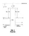
- FIG. 1shows a typical prior art electron energy diagram for a flash memory cell.
- FIG. 2shows a cross-sectional view of one embodiment of a flash memory cell transistor of the present invention having a graded composition, high dielectric constant gate insulator.
- FIG. 3shows one embodiment of an electron energy band diagram in accordance with the graded composition, high dielectric constant gate insulator transistor structure of FIG. 2 .
- FIG. 4shows an electron energy band diagram in accordance with another embodiment of the graded composition, high dielectric constant gate insulator transistor structure of FIG. 2 .
- FIG. 5shows a plot of band gap energies versus electron affinities in accordance with the embodiments of the present invention.
- FIG. 6shows a band diagram for amorphous silicon carbide on silicon in accordance with the embodiments of the present invention.
- FIG. 7shows a band diagram for germanium carbide on germanium in accordance with the embodiments of the present invention.
- FIG. 8shows a block diagram of an electronic system of the present invention.
- SOSsilicon-on-sapphire
- SOIsilicon-on-insulator
- TFTthin film transistor
- doped and undoped semiconductorsepitaxial layers of a silicon supported by a base semiconductor structure, as well as other semiconductor structures well known to one skilled in the art.
- wafer or substratewhen reference is made to a wafer or substrate in the following description, previous process steps may have been utilized to form regions/junctions in the base semiconductor structure, and terms wafer or substrate include the underlying layers containing such regions/junctions.
- FIG. 2illustrates a cross-sectional view of one embodiment of a flash memory cell transistor of the present invention.
- the transistorhas a graded composition, high dielectric constant (i.e., high-K) gate dielectric.
- the transistorcomprises a pair of source/drain regions 201 and 202 implanted in a silicon substrate 211 .
- the direction of operation of the transistordetermines which region 201 or 202 functions as a source and which functions as a drain.
- a channel region 203exists between the source/drain regions 201 and 202 .
- the substrate 211comprises germanium.
- the source/drain regions 201 and 202are n+ doped regions in a p+ type substrate 211 .
- An alternate embodimentmay use p+ doped source/drain regions in an n+ type substrate.
- the present inventionis not limited to any one conductivity type for the source/drain regions or the substrate.
- a high-permittivity (high-K), graded composition tunnel gate dielectric 206is formed over the substrate 211 substantially between the source/drain regions 201 and 202 and over the channel region 203 .
- the tunnel gate dielectric 206is amorphous germanium carbide or graded composition amorphous germanium-silicon carbide that provide adjustable barrier heights in contact with the substrate 211 and floating gate layer 208 .
- a floating gate layer 208is formed over the tunnel gate dielectric layer 206 .
- a gate insulator layer 210is formed over the floating gate 208 .
- a control gate 212is formed on top of the gate insulator layer 210 .
- the floating gate layer 208 and the control gate 212are a polysilicon material and the gate insulator layer 210 is an interpoly insulator.
- the architecture of the flash memory cell transistor of FIG. 2is for purposes of illustration only.
- the amorphous germanium carbide and graded composition amorphous germanium-silicon carbide tunnel dielectric of the present inventionis not limited to planar transistors as illustrated in FIG. 2 . This type of tunnel dielectric can be used in other types of planar transistors as well as vertical transistors.
- a high dielectric constantis considered to be a dielectric constant that is greater than that of SiO 2 .
- a wide variety of different high dielectric constant insulatorscan be realized using atomic layer deposition (ALD) or evaporation techniques. An example of such dielectric materials and their characteristics are summarized in the following table:
- the high-K dielectric materials of the present inventioncan be used as graded composition in either the tunnel gate dielectric 206 or the gate insulator layer 210 .
- the barriers and/or tunnel barrierscan either be reduced between the silicon and the gate dielectric as illustrated in FIG. 3 or between the floating gate and the gate insulating dielectric as illustrated in FIG. 4 .
- FIG. 3illustrates an electron energy band diagram in accordance with the graded composition, high dielectric constant gate insulator transistor structure of FIG. 2 .
- the graded compositionin one embodiment, is silicon carbide to germanium carbide that is graded in the direction shown from silicon carbide closest to the silicon substrate to germanium carbide closest to the polysilicon floating gate.
- This compositioncould be deposited on a silicon carbide gate insulator formed by carburization of silicon. Alternate embodiments could use other techniques for the deposition of silicon carbide and germanium carbide.
- An alternate embodimentuses a graded composition of silicon oxide to silicon carbide to germanium carbide. As illustrated in FIG. 3 , the tunnel gate insulator is graded from silicon oxide nearest the substrate to silicon carbide to germanium carbide nearest the floating gate.
- the gate insulatorcomprises amorphous germanium carbide. As seen in the table above and the plot of FIG. 5 , this composition also provides a lower band gap and larger electron affinity than prior art materials such as SiO 2 .
- FIG. 4illustrates an electron energy band diagram in accordance with another embodiment of the graded composition, high dielectric constant gate insulator transistor structure of FIG. 2 .
- the graded compositionin one embodiment, is silicon carbide to germanium carbide.
- the gate insulatoris graded in the direction shown from silicon carbide nearest the polysilicon floating gate to germanium carbide nearest the silicon substrate.
- FIG. 4shows that this graded composition results in a low barrier at the polysilicon floating gate-gate insulator interface.
- the germanium carbideis deposited on the silicon substrate or a thin layer of silicon oxide and the composition graded towards silicon carbide as the tunnel gate insulator is further deposited. Alternate embodiments can use other techniques for forming this layer.
- the tunnel gate insulatorcomprises a graded composition of silicon oxide to silicon carbide to germanium carbide. As indicated in the figure, the silicon oxide is formed closest to the floating gate while the germanium carbide is formed closest to the silicon substrate.
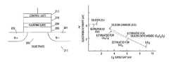
- FIG. 5illustrates a plot of electron affinity versus band gap energy of silicon, silicon carbide (SiC), Germanium, and Germanium Carbide (Ge X C Y ).
- SiCsilicon carbide
- GermaniumGermanium Carbide
- FIG. 5illustrates a plot of electron affinity versus band gap energy of silicon, silicon carbide (SiC), Germanium, and Germanium Carbide (Ge X C Y ).
- prior art insulator silicon dioxidehas a relative dielectric constant of 3.9, energy gap of approximately 9.0 eV, and electron affinity of 0.9 eV.
- electrons stored on the polysilicon floating gatesee a large tunneling barrier of about 3.2 eV. This value is the difference between the electron affinities of silicon (4.1 eV) and SiO 2 (0.9 eV). This is a relatively large barrier that requires high applied electric fields for electron injection.
- SiChas a band gap of 3 eV and an electron affinity of 3.7 eV.
- Amorphous SiChas relatively low conductivity under modest applied electric fields.
- Ge X C Yhas an estimated band gap of 2.5 eV and an electron affinity of 3.0 eV. Both have a much larger electron affinity and a much smaller barrier than SiO 2 that requires a much lower applied electric field for electron injection.
- FIG. 6illustrates a band diagram for amorphous silicon carbide on silicon in accordance with the embodiments of the present invention. If amorphous hydrogenated silicon carbide is deposited with a gap of up to 3.4 eV, amorphous silicon carbide can then have a band gap of greater than 2.1 eV of crystalline SiC and an electron affinity of less than 3.7 eV. Amorphous silicon carbide on silicon has a low surface recombination velocity and excellent passivation on silicon as compared to the prior art silicon dioxide.
- FIG. 7illustrates a band diagram for germanium carbide on germanium in accordance with the embodiments of the present invention.
- Microcrystalline hydrogenated germanium carbide filmshave been deposited by RF sputtering and electron cyclotron resonance plasma processing. With a low carbon concentration of 4%, these have a band gap energy of around that of silicon (i.e., 1.2 eV).
- Amorphous hydrogenated germanium carbidecan be deposited as an insulator and it can have, after annealing, a band gap energy as high as 7.1 eV and an electron affinity of 1.2 eV.
- Amorphous germanium carbide on germaniumcan have an energy barrier of up to 2.8 eV and is therefore suitable for passivation and a dielectric insulator.
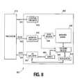
- FIG. 8illustrates a functional block diagram of a memory device 800 that can incorporate the flash memory cells of the present invention.
- the memory device 800is coupled to a processor 810 .
- the processor 810may be a microprocessor or some other type of controlling circuitry.
- the memory device 800 and the processor 810form part of an electronic system 820 .
- the memory device 800has been simplified to focus on features of the memory that are helpful in understanding the present invention.
- the memory deviceincludes an array of flash memory cells 830 .
- the memory array 830is arranged in banks of rows and columns.
- the control gates of each row of memory cellsis coupled with a wordline while the drain and source connections of the memory cells are coupled to bitlines.
- the connection of the cells to the bitlinesdepends on whether the array is a NAND architecture, a NOR architecture, or some other array architecture.
- the flash memory cells of the present inventionare not limited to any one architecture.
- An address buffer circuit 840is provided to latch address signals provided on address input connections A0-Ax 842 . Address signals are received and decoded by a row decoder 844 and a column decoder 846 to access the memory array 830 . It will be appreciated by those skilled in the art, with the benefit of the present description, that the number of address input connections depends on the density and architecture of the memory array 830 . That is, the number of addresses increases with both increased memory cell counts and increased bank and block counts.
- the memory device 800reads data in the memory array 830 by sensing voltage or current changes in the memory array columns using sense/buffer circuitry 850 .
- the sense/buffer circuitryin one embodiment, is coupled to read and latch a row of data from the memory array 830 .
- Data input and output buffer circuitry 860is included for bi-directional data communication over a plurality of data connections 862 with the controller 810 ).
- Write circuitry 855is provided to write data to the memory array.
- Control circuitry 870decodes signals provided on control connections 872 from the processor 810 . These signals are used to control the operations on the memory array 830 , including data read, data write, and erase operations.
- the control circuitry 870may be a state machine, a sequencer, or some other type of controller.
- the flash memory device illustrated in FIG. 8has been simplified to facilitate a basic understanding of the features of the memory. A more detailed understanding of internal circuitry and functions of flash memories are known to those skilled in the art.
- flash memory transistors of the present invention with graded composition, high-K gate dielectricsreduce the electron barrier between the substrate and gate insulator and the tunnel barrier between the polysilicon floating gate and gate insulator. This is accomplished by using a graded composition, high-K dielectric gate insulator instead of the prior art's silicon dioxide.
- the use of the gate insulators described aboveallows for two different barriers.
- the lower height of the tunneling barriers with high-K dielectric gate insulatorscan provide larger tunneling currents out of the floating gate with smaller control gate voltages.
- the lower barrier at the interface with the silicon substratemakes the write operation easier and write currents by channel hot electron injection larger at lower voltages. Both tunneling currents and hot electron injection currents are exponential functions of the barrier heights and electric fields.
- the higher dielectric constant gate insulators of the present inventionalso allow for better scaling of flash memory devices to smaller dimensions.
- the effective gate length of high-K gate tunneling dielectric flash memory transistorscan be scaled below 50 nm.
- High-k gate dielectricsreduce or eliminate drain turn-on problems, short-channel effects and punchthrough in flash memory transistors.
- Smaller write and erase voltagesprovide another advantage in that the thickness of the SiO 2 or other insulator layer between the control gate and the floating gate can be reduced.
Landscapes
- Non-Volatile Memory (AREA)
- Semiconductor Memories (AREA)
Abstract
Description
| Dielectric | Band Gap | Delta Ec(eV) | |||
| Material | Constant (K) | Ec(eV) | to Si | ||
| SiO2 | 3.9 | 8.9 | 3.2 | ||
| Si3N4 | 7 | 5.1 | 2 | ||
| Al2O3 | 9 | 8.7 | 2.8 | ||
| Y2O3 | 15 | 5.6 | 2.3 | ||
| La2O3 | 30 | 4.3 | 2.3 | ||
| Ta2O5 | 26 | 4.5 | 1-1.5 | ||
| TiO2 | 80 | 3.5 | 1.2 | ||
| HfO2 | 25 | 5.7 | 1.5 | ||
| ZrO2 | 25 | 7.8 | 1.4 | ||
| 10 | 3.4 | 1.1 | |||
| GeXCY | 12 (est.) | 5.7 | 2.2 | ||
Claims (21)
Priority Applications (1)
| Application Number | Priority Date | Filing Date | Title |
|---|---|---|---|
| US13/595,219US8786006B2 (en) | 2005-04-26 | 2012-08-27 | Flash memory device having a graded composition, high dielectric constant gate insulator |
Applications Claiming Priority (4)
| Application Number | Priority Date | Filing Date | Title |
|---|---|---|---|
| US11/114,403US7253469B2 (en) | 2005-04-26 | 2005-04-26 | Flash memory device having a graded composition, high dielectric constant gate insulator |
| US11/811,609US7892921B2 (en) | 2005-04-26 | 2007-06-11 | Flash memory device having a graded composition, high dielectric constant gate insulator |
| US13/023,609US8258518B2 (en) | 2005-04-26 | 2011-02-09 | Flash memory device having a graded composition, high dielectric constant gate insulator |
| US13/595,219US8786006B2 (en) | 2005-04-26 | 2012-08-27 | Flash memory device having a graded composition, high dielectric constant gate insulator |
Related Parent Applications (1)
| Application Number | Title | Priority Date | Filing Date |
|---|---|---|---|
| US13/023,609DivisionUS8258518B2 (en) | 2005-04-26 | 2011-02-09 | Flash memory device having a graded composition, high dielectric constant gate insulator |
Publications (2)
| Publication Number | Publication Date |
|---|---|
| US20120313097A1 US20120313097A1 (en) | 2012-12-13 |
| US8786006B2true US8786006B2 (en) | 2014-07-22 |
Family
ID=37185963
Family Applications (4)
| Application Number | Title | Priority Date | Filing Date |
|---|---|---|---|
| US11/114,403Expired - LifetimeUS7253469B2 (en) | 2005-04-26 | 2005-04-26 | Flash memory device having a graded composition, high dielectric constant gate insulator |
| US11/811,609Active2026-06-03US7892921B2 (en) | 2005-04-26 | 2007-06-11 | Flash memory device having a graded composition, high dielectric constant gate insulator |
| US13/023,609Expired - LifetimeUS8258518B2 (en) | 2005-04-26 | 2011-02-09 | Flash memory device having a graded composition, high dielectric constant gate insulator |
| US13/595,219Expired - LifetimeUS8786006B2 (en) | 2005-04-26 | 2012-08-27 | Flash memory device having a graded composition, high dielectric constant gate insulator |
Family Applications Before (3)
| Application Number | Title | Priority Date | Filing Date |
|---|---|---|---|
| US11/114,403Expired - LifetimeUS7253469B2 (en) | 2005-04-26 | 2005-04-26 | Flash memory device having a graded composition, high dielectric constant gate insulator |
| US11/811,609Active2026-06-03US7892921B2 (en) | 2005-04-26 | 2007-06-11 | Flash memory device having a graded composition, high dielectric constant gate insulator |
| US13/023,609Expired - LifetimeUS8258518B2 (en) | 2005-04-26 | 2011-02-09 | Flash memory device having a graded composition, high dielectric constant gate insulator |
Country Status (1)
| Country | Link |
|---|---|
| US (4) | US7253469B2 (en) |
Families Citing this family (12)
| Publication number | Priority date | Publication date | Assignee | Title |
|---|---|---|---|---|
| EP1837917A1 (en)* | 2006-03-21 | 2007-09-26 | Semiconductor Energy Laboratory Co., Ltd. | Nonvolatile semiconductor memory device |
| JP4976796B2 (en)* | 2006-09-25 | 2012-07-18 | 株式会社東芝 | Semiconductor device |
| RU2343587C2 (en)* | 2006-12-07 | 2009-01-10 | Федеральное государственное образовательное учреждение высшего профессионального образования Санкт-Петербургский государственный университет (СПбГУ) | Memory device with dielectric layer based on dielectric films and method of its producing |
| JP5222628B2 (en)* | 2007-05-31 | 2013-06-26 | 株式会社半導体エネルギー研究所 | Semiconductor device |
| RU2357324C1 (en)* | 2008-01-09 | 2009-05-27 | Институт физики полупроводников Сибирского отделения Российской академии наук | Flash memory element for electrically programmable read-only memory |
| RU2368037C1 (en)* | 2008-06-04 | 2009-09-20 | Институт физики полупроводников Сибирского отделения Российской академии наук | Flash memory element of electrically alterable read-only memory |
| US9209314B2 (en)* | 2010-06-16 | 2015-12-08 | Semiconductor Energy Laboratory Co., Ltd. | Field effect transistor |
| US9318336B2 (en) | 2011-10-27 | 2016-04-19 | Globalfoundries U.S. 2 Llc | Non-volatile memory structure employing high-k gate dielectric and metal gate |
| CN103346168B (en)* | 2013-06-20 | 2016-02-24 | 华中科技大学 | Based on SiC xsilicon quantum dot floating gate non-volatile memory of texture and preparation method thereof |
| US9406689B2 (en)* | 2013-07-31 | 2016-08-02 | Qualcomm Incorporated | Logic finFET high-K/conductive gate embedded multiple time programmable flash memory |
| US10242989B2 (en)* | 2014-05-20 | 2019-03-26 | Micron Technology, Inc. | Polar, chiral, and non-centro-symmetric ferroelectric materials, memory cells including such materials, and related devices and methods |
| US9953839B2 (en)* | 2016-08-18 | 2018-04-24 | International Business Machines Corporation | Gate-stack structure with a diffusion barrier material |
Citations (12)
| Publication number | Priority date | Publication date | Assignee | Title |
|---|---|---|---|---|
| US5731045A (en) | 1996-01-26 | 1998-03-24 | Southwest Research Institute | Application of diamond-like carbon coatings to cobalt-cemented tungsten carbide components |
| US5770501A (en) | 1995-12-22 | 1998-06-23 | United Microelectronics Corporation | Process of fabricating NAND-structure flash EEPROM using liquid phase deposition |
| US6335238B1 (en) | 1997-05-08 | 2002-01-01 | Texas Instruments Incorporated | Integrated dielectric and method |
| US20020025626A1 (en) | 1998-05-05 | 2002-02-28 | Sunil Hattangady | Integrated dielectric and method |
| US6511872B1 (en) | 2001-07-10 | 2003-01-28 | Agere Systems Inc. | Device having a high dielectric constant material and a method of manufacture thereof |
| US20030042527A1 (en) | 2001-08-30 | 2003-03-06 | Micron Technology, Inc. | Programmable array logic or memory devices with asymmetrical tunnel barriers |
| US20030048666A1 (en) | 2001-08-30 | 2003-03-13 | Micron Technology, Inc. | Graded composition metal oxide tunnel barrier interpoly insulators |
| US20030049900A1 (en) | 2001-08-30 | 2003-03-13 | Micron Technology Inc. | Graded composition gate insulators to reduce tunneling barriers in flash memory devices |
| US20030193062A1 (en) | 2002-04-16 | 2003-10-16 | Fuh-Cheng Jong | Nonvolatile memory cell for prevention from second bit effect |
| US6794255B1 (en) | 1997-07-29 | 2004-09-21 | Micron Technology, Inc. | Carburized silicon gate insulators for integrated circuits |
| US20040262699A1 (en) | 2003-06-30 | 2004-12-30 | Rafael Rios | N-gate transistor |
| US20060043463A1 (en) | 2004-09-01 | 2006-03-02 | Taiwan Semiconductor Manufacturing Company, Ltd. | Floating gate having enhanced charge retention |
Family Cites Families (2)
| Publication number | Priority date | Publication date | Assignee | Title |
|---|---|---|---|---|
| US20030020086A1 (en)* | 2001-07-25 | 2003-01-30 | Motorola, Inc. | Tuned delay components for an integrated circuit |
| US7759719B2 (en)* | 2004-07-01 | 2010-07-20 | Chih-Hsin Wang | Electrically alterable memory cell |
- 2005
- 2005-04-26USUS11/114,403patent/US7253469B2/ennot_activeExpired - Lifetime
- 2007
- 2007-06-11USUS11/811,609patent/US7892921B2/enactiveActive
- 2011
- 2011-02-09USUS13/023,609patent/US8258518B2/ennot_activeExpired - Lifetime
- 2012
- 2012-08-27USUS13/595,219patent/US8786006B2/ennot_activeExpired - Lifetime
Patent Citations (13)
| Publication number | Priority date | Publication date | Assignee | Title |
|---|---|---|---|---|
| US5770501A (en) | 1995-12-22 | 1998-06-23 | United Microelectronics Corporation | Process of fabricating NAND-structure flash EEPROM using liquid phase deposition |
| US5731045A (en) | 1996-01-26 | 1998-03-24 | Southwest Research Institute | Application of diamond-like carbon coatings to cobalt-cemented tungsten carbide components |
| US6335238B1 (en) | 1997-05-08 | 2002-01-01 | Texas Instruments Incorporated | Integrated dielectric and method |
| US6794255B1 (en) | 1997-07-29 | 2004-09-21 | Micron Technology, Inc. | Carburized silicon gate insulators for integrated circuits |
| US20020025626A1 (en) | 1998-05-05 | 2002-02-28 | Sunil Hattangady | Integrated dielectric and method |
| US6511872B1 (en) | 2001-07-10 | 2003-01-28 | Agere Systems Inc. | Device having a high dielectric constant material and a method of manufacture thereof |
| US20030048666A1 (en) | 2001-08-30 | 2003-03-13 | Micron Technology, Inc. | Graded composition metal oxide tunnel barrier interpoly insulators |
| US20030049900A1 (en) | 2001-08-30 | 2003-03-13 | Micron Technology Inc. | Graded composition gate insulators to reduce tunneling barriers in flash memory devices |
| US6586797B2 (en) | 2001-08-30 | 2003-07-01 | Micron Technology, Inc. | Graded composition gate insulators to reduce tunneling barriers in flash memory devices |
| US20030042527A1 (en) | 2001-08-30 | 2003-03-06 | Micron Technology, Inc. | Programmable array logic or memory devices with asymmetrical tunnel barriers |
| US20030193062A1 (en) | 2002-04-16 | 2003-10-16 | Fuh-Cheng Jong | Nonvolatile memory cell for prevention from second bit effect |
| US20040262699A1 (en) | 2003-06-30 | 2004-12-30 | Rafael Rios | N-gate transistor |
| US20060043463A1 (en) | 2004-09-01 | 2006-03-02 | Taiwan Semiconductor Manufacturing Company, Ltd. | Floating gate having enhanced charge retention |
Non-Patent Citations (16)
| Title |
|---|
| A.H. Mahan et al., On the influence of short and medium range order on the material band gap in hydrogenated amorphous silicon, Journal of Applied Physics, vol. 96, No. 7, Oct. 2004, pp. 3818-3826. |
| Booth et al., The optical and structural properties of CVD germanium carbide., Journal de Physique Colloque (France), vol. 42, No. C-4, pt.2, Oct. 1981, pp. 1033-1036. |
| C. Summonte et al., Wide band-gap silicon-carbon alloys deposited by very high frequency plasma enhanced chemical vapor deposition, Journal of Applied Physics, vol. 96 No. 7, Oct. 2004, pp. 3987-3997. |
| Gong et al., Asymmetric electron spin resonance signals in hydrogenated amorphous germanium carbide films, Physica Status Solidi B (Germany) vol. 172 No. 1, Jul. 1992, pp. K1-5. |
| J. Tyczkowski et al., Electronic band structure of insulating hydrogenated carbon-germanium films, Journal of Applied Physics, vol. 86, No. 8, Oct. 1999, pp. 4412-4418. |
| Kelly et al., Application of germanium carbide in durable multiplaver IR coatings., Hard Materials in Optics, The Hague, Netherlands, Mar. 14-15, 1990. |
| Kumru, M., A comparison of the optical, IR, electron spin resonance and conductivity properties of a Ge/subl-x/C/subx/:H with a Ge:H and a Ge thin films prepared by RF sputtering, Thin Solid Films (Switzerland), vol. 198, No. 1-2, Mar. 1991, pp. 75-84. |
| L. Vikram et al., Microcrystalline Germanium Carbide-A new material for PV conversion, Iowa State University, Dept. of Electrical and Computer Engr., Ames, Iowa, pp. 348-349. |
| L. Vikram et al., Microcrystalline Germanium Carbide—A new material for PV conversion, Iowa State University, Dept. of Electrical and Computer Engr., Ames, Iowa, pp. 348-349. |
| Liu et al., Structure and properties of germanium carbide films prepared by RF reactive sputtering in Ar/CH/sub 4/., Japanese Journal of Applied Physics Part 1 vol. 36, No. 6A, Jun. 1997, pp. 3625-3628. |
| M. Vetter et al., IR-study of a SiC/sub x/:H and a-SiC/sub x/N/sub y/:H films for c-Si surface passivation, Thin Solid Films, vol. 451-452, Mar. 22, 2004, pp. 340-344. |
| M. Vetter et al., IR—study of a SiC/sub x/:H and a-SiC/sub x/N/sub y/:H films for c-Si surface passivation, Thin Solid Films, vol. 451-452, Mar. 22, 2004, pp. 340-344. |
| P. Pavan et al., Flash Memory Cells-An Overview, Proceedings of the IEEE, vol. 85, No. 8, Aug. 1997, pp. 1248-1271. |
| P. Pavan et al., Flash Memory Cells—An Overview, Proceedings of the IEEE, vol. 85, No. 8, Aug. 1997, pp. 1248-1271. |
| R. Shinar et al., Electron energy-loss studies on radio frequency sputtered a-Ge1-xCx: H films , Journal Vac. Sci. Technology A, vol. 5, No. 5, Sep./Oct. 1987, pp. 2804-2808. |
| R. Shinar, Hydrogen adsorption on some a-Ge1-xCx:H films prepared by radio frequency sputtering, Journal Vac. Sci. Technology A, vol. 6, No. 5, Sep./Oct. 1988, pp. 2910-2913. |
Also Published As
| Publication number | Publication date |
|---|---|
| US20110127598A1 (en) | 2011-06-02 |
| US8258518B2 (en) | 2012-09-04 |
| US7253469B2 (en) | 2007-08-07 |
| US20060237771A1 (en) | 2006-10-26 |
| US7892921B2 (en) | 2011-02-22 |
| US20070243682A1 (en) | 2007-10-18 |
| US20120313097A1 (en) | 2012-12-13 |
Similar Documents
| Publication | Publication Date | Title |
|---|---|---|
| US8786006B2 (en) | Flash memory device having a graded composition, high dielectric constant gate insulator | |
| US7683424B2 (en) | Ballistic direct injection NROM cell on strained silicon structures | |
| US8404536B2 (en) | Method for fabricating stacked non-volatile memory with silicon carbide-based amorphous silicon thin film transistors | |
| US8093638B2 (en) | Systems with a gate dielectric having multiple lanthanide oxide layers | |
| US7276413B2 (en) | NROM flash memory devices on ultrathin silicon | |
| US7672171B2 (en) | Non-planar flash memory array with shielded floating gates on silicon mesas | |
| US20060284244A1 (en) | Erasable non-volatile memory device using hole trapping in high-k dielectrics | |
| US20070034922A1 (en) | Integrated surround gate multifunctional memory device | |
| US6750502B1 (en) | Technique to quench electrical defects in aluminum oxide film | |
| US20060273370A1 (en) | NROM flash memory with vertical transistors and surrounding gates | |
| US7198999B2 (en) | Flash memory device having a graded composition, high dielectric constant gate insulator | |
| US7221597B2 (en) | Ballistic direct injection flash memory cell on strained silicon structures | |
| US7271437B2 (en) | Non-volatile memory with hole trapping barrier | |
| US20060003516A1 (en) | Flash memory devices on silicon carbide |
Legal Events
| Date | Code | Title | Description |
|---|---|---|---|
| FEPP | Fee payment procedure | Free format text:PAYOR NUMBER ASSIGNED (ORIGINAL EVENT CODE: ASPN); ENTITY STATUS OF PATENT OWNER: LARGE ENTITY | |
| STCF | Information on status: patent grant | Free format text:PATENTED CASE | |
| AS | Assignment | Owner name:U.S. BANK NATIONAL ASSOCIATION, AS COLLATERAL AGENT, CALIFORNIA Free format text:SECURITY INTEREST;ASSIGNOR:MICRON TECHNOLOGY, INC.;REEL/FRAME:038669/0001 Effective date:20160426 Owner name:U.S. BANK NATIONAL ASSOCIATION, AS COLLATERAL AGEN Free format text:SECURITY INTEREST;ASSIGNOR:MICRON TECHNOLOGY, INC.;REEL/FRAME:038669/0001 Effective date:20160426 | |
| AS | Assignment | Owner name:MORGAN STANLEY SENIOR FUNDING, INC., AS COLLATERAL AGENT, MARYLAND Free format text:PATENT SECURITY AGREEMENT;ASSIGNOR:MICRON TECHNOLOGY, INC.;REEL/FRAME:038954/0001 Effective date:20160426 Owner name:MORGAN STANLEY SENIOR FUNDING, INC., AS COLLATERAL Free format text:PATENT SECURITY AGREEMENT;ASSIGNOR:MICRON TECHNOLOGY, INC.;REEL/FRAME:038954/0001 Effective date:20160426 | |
| AS | Assignment | Owner name:U.S. BANK NATIONAL ASSOCIATION, AS COLLATERAL AGENT, CALIFORNIA Free format text:CORRECTIVE ASSIGNMENT TO CORRECT THE REPLACE ERRONEOUSLY FILED PATENT #7358718 WITH THE CORRECT PATENT #7358178 PREVIOUSLY RECORDED ON REEL 038669 FRAME 0001. ASSIGNOR(S) HEREBY CONFIRMS THE SECURITY INTEREST;ASSIGNOR:MICRON TECHNOLOGY, INC.;REEL/FRAME:043079/0001 Effective date:20160426 Owner name:U.S. BANK NATIONAL ASSOCIATION, AS COLLATERAL AGEN Free format text:CORRECTIVE ASSIGNMENT TO CORRECT THE REPLACE ERRONEOUSLY FILED PATENT #7358718 WITH THE CORRECT PATENT #7358178 PREVIOUSLY RECORDED ON REEL 038669 FRAME 0001. ASSIGNOR(S) HEREBY CONFIRMS THE SECURITY INTEREST;ASSIGNOR:MICRON TECHNOLOGY, INC.;REEL/FRAME:043079/0001 Effective date:20160426 | |
| MAFP | Maintenance fee payment | Free format text:PAYMENT OF MAINTENANCE FEE, 4TH YEAR, LARGE ENTITY (ORIGINAL EVENT CODE: M1551) Year of fee payment:4 | |
| AS | Assignment | Owner name:JPMORGAN CHASE BANK, N.A., AS COLLATERAL AGENT, ILLINOIS Free format text:SECURITY INTEREST;ASSIGNORS:MICRON TECHNOLOGY, INC.;MICRON SEMICONDUCTOR PRODUCTS, INC.;REEL/FRAME:047540/0001 Effective date:20180703 Owner name:JPMORGAN CHASE BANK, N.A., AS COLLATERAL AGENT, IL Free format text:SECURITY INTEREST;ASSIGNORS:MICRON TECHNOLOGY, INC.;MICRON SEMICONDUCTOR PRODUCTS, INC.;REEL/FRAME:047540/0001 Effective date:20180703 | |
| AS | Assignment | Owner name:MICRON TECHNOLOGY, INC., IDAHO Free format text:RELEASE BY SECURED PARTY;ASSIGNOR:U.S. BANK NATIONAL ASSOCIATION, AS COLLATERAL AGENT;REEL/FRAME:047243/0001 Effective date:20180629 | |
| AS | Assignment | Owner name:MICRON TECHNOLOGY, INC., IDAHO Free format text:RELEASE BY SECURED PARTY;ASSIGNOR:MORGAN STANLEY SENIOR FUNDING, INC., AS COLLATERAL AGENT;REEL/FRAME:050937/0001 Effective date:20190731 | |
| AS | Assignment | Owner name:MICRON SEMICONDUCTOR PRODUCTS, INC., IDAHO Free format text:RELEASE BY SECURED PARTY;ASSIGNOR:JPMORGAN CHASE BANK, N.A., AS COLLATERAL AGENT;REEL/FRAME:051028/0001 Effective date:20190731 Owner name:MICRON TECHNOLOGY, INC., IDAHO Free format text:RELEASE BY SECURED PARTY;ASSIGNOR:JPMORGAN CHASE BANK, N.A., AS COLLATERAL AGENT;REEL/FRAME:051028/0001 Effective date:20190731 | |
| MAFP | Maintenance fee payment | Free format text:PAYMENT OF MAINTENANCE FEE, 8TH YEAR, LARGE ENTITY (ORIGINAL EVENT CODE: M1552); ENTITY STATUS OF PATENT OWNER: LARGE ENTITY Year of fee payment:8 |