US8784974B2 - Sub-10 NM line features via rapid graphoepitaxial self-assembly of amphiphilic monolayers - Google Patents
Sub-10 NM line features via rapid graphoepitaxial self-assembly of amphiphilic monolayersDownload PDFInfo
- Publication number
- US8784974B2 US8784974B2US13/473,748US201213473748AUS8784974B2US 8784974 B2US8784974 B2US 8784974B2US 201213473748 AUS201213473748 AUS 201213473748AUS 8784974 B2US8784974 B2US 8784974B2
- Authority
- US
- United States
- Prior art keywords
- trench
- substrate
- sidewalls
- floor
- cross
- Prior art date
- Legal status (The legal status is an assumption and is not a legal conclusion. Google has not performed a legal analysis and makes no representation as to the accuracy of the status listed.)
- Active
Links
Images


Classifications
- B—PERFORMING OPERATIONS; TRANSPORTING
- B81—MICROSTRUCTURAL TECHNOLOGY
- B81C—PROCESSES OR APPARATUS SPECIALLY ADAPTED FOR THE MANUFACTURE OR TREATMENT OF MICROSTRUCTURAL DEVICES OR SYSTEMS
- B81C1/00—Manufacture or treatment of devices or systems in or on a substrate
- B81C1/00015—Manufacture or treatment of devices or systems in or on a substrate for manufacturing microsystems
- B81C1/00023—Manufacture or treatment of devices or systems in or on a substrate for manufacturing microsystems without movable or flexible elements
- B81C1/00031—Regular or irregular arrays of nanoscale structures, e.g. etch mask layer
- H—ELECTRICITY
- H01—ELECTRIC ELEMENTS
- H01L—SEMICONDUCTOR DEVICES NOT COVERED BY CLASS H10
- H01L21/00—Processes or apparatus adapted for the manufacture or treatment of semiconductor or solid state devices or of parts thereof
- H01L21/02—Manufacture or treatment of semiconductor devices or of parts thereof
- H01L21/02002—Preparing wafers
- B—PERFORMING OPERATIONS; TRANSPORTING
- B05—SPRAYING OR ATOMISING IN GENERAL; APPLYING FLUENT MATERIALS TO SURFACES, IN GENERAL
- B05D—PROCESSES FOR APPLYING FLUENT MATERIALS TO SURFACES, IN GENERAL
- B05D3/00—Pretreatment of surfaces to which liquids or other fluent materials are to be applied; After-treatment of applied coatings, e.g. intermediate treating of an applied coating preparatory to subsequent applications of liquids or other fluent materials
- B05D3/007—After-treatment
- B—PERFORMING OPERATIONS; TRANSPORTING
- B82—NANOTECHNOLOGY
- B82Y—SPECIFIC USES OR APPLICATIONS OF NANOSTRUCTURES; MEASUREMENT OR ANALYSIS OF NANOSTRUCTURES; MANUFACTURE OR TREATMENT OF NANOSTRUCTURES
- B82Y30/00—Nanotechnology for materials or surface science, e.g. nanocomposites
- H—ELECTRICITY
- H01—ELECTRIC ELEMENTS
- H01L—SEMICONDUCTOR DEVICES NOT COVERED BY CLASS H10
- H01L21/00—Processes or apparatus adapted for the manufacture or treatment of semiconductor or solid state devices or of parts thereof
- H01L21/02—Manufacture or treatment of semiconductor devices or of parts thereof
- H01L21/04—Manufacture or treatment of semiconductor devices or of parts thereof the devices having potential barriers, e.g. a PN junction, depletion layer or carrier concentration layer
- H01L21/18—Manufacture or treatment of semiconductor devices or of parts thereof the devices having potential barriers, e.g. a PN junction, depletion layer or carrier concentration layer the devices having semiconductor bodies comprising elements of Group IV of the Periodic Table or AIIIBV compounds with or without impurities, e.g. doping materials
- H01L21/30—Treatment of semiconductor bodies using processes or apparatus not provided for in groups H01L21/20 - H01L21/26
- H01L21/302—Treatment of semiconductor bodies using processes or apparatus not provided for in groups H01L21/20 - H01L21/26 to change their surface-physical characteristics or shape, e.g. etching, polishing, cutting
- H01L21/306—Chemical or electrical treatment, e.g. electrolytic etching
- H01L21/308—Chemical or electrical treatment, e.g. electrolytic etching using masks
- H01L21/3083—Chemical or electrical treatment, e.g. electrolytic etching using masks characterised by their size, orientation, disposition, behaviour, shape, in horizontal or vertical plane
- H01L21/3086—Chemical or electrical treatment, e.g. electrolytic etching using masks characterised by their size, orientation, disposition, behaviour, shape, in horizontal or vertical plane characterised by the process involved to create the mask, e.g. lift-off masks, sidewalls, or to modify the mask, e.g. pre-treatment, post-treatment
- H—ELECTRICITY
- H01—ELECTRIC ELEMENTS
- H01L—SEMICONDUCTOR DEVICES NOT COVERED BY CLASS H10
- H01L21/00—Processes or apparatus adapted for the manufacture or treatment of semiconductor or solid state devices or of parts thereof
- H01L21/02—Manufacture or treatment of semiconductor devices or of parts thereof
- H01L21/04—Manufacture or treatment of semiconductor devices or of parts thereof the devices having potential barriers, e.g. a PN junction, depletion layer or carrier concentration layer
- H01L21/18—Manufacture or treatment of semiconductor devices or of parts thereof the devices having potential barriers, e.g. a PN junction, depletion layer or carrier concentration layer the devices having semiconductor bodies comprising elements of Group IV of the Periodic Table or AIIIBV compounds with or without impurities, e.g. doping materials
- H01L21/30—Treatment of semiconductor bodies using processes or apparatus not provided for in groups H01L21/20 - H01L21/26
- H01L21/31—Treatment of semiconductor bodies using processes or apparatus not provided for in groups H01L21/20 - H01L21/26 to form insulating layers thereon, e.g. for masking or by using photolithographic techniques; After treatment of these layers; Selection of materials for these layers
- H01L21/3105—After-treatment
- H01L21/311—Etching the insulating layers by chemical or physical means
- H01L21/31144—Etching the insulating layers by chemical or physical means using masks
- B—PERFORMING OPERATIONS; TRANSPORTING
- B81—MICROSTRUCTURAL TECHNOLOGY
- B81C—PROCESSES OR APPARATUS SPECIALLY ADAPTED FOR THE MANUFACTURE OR TREATMENT OF MICROSTRUCTURAL DEVICES OR SYSTEMS
- B81C2201/00—Manufacture or treatment of microstructural devices or systems
- B81C2201/01—Manufacture or treatment of microstructural devices or systems in or on a substrate
- B81C2201/0101—Shaping material; Structuring the bulk substrate or layers on the substrate; Film patterning
- B81C2201/0147—Film patterning
- B81C2201/0149—Forming nanoscale microstructures using auto-arranging or self-assembling material
- B—PERFORMING OPERATIONS; TRANSPORTING
- B81—MICROSTRUCTURAL TECHNOLOGY
- B81C—PROCESSES OR APPARATUS SPECIALLY ADAPTED FOR THE MANUFACTURE OR TREATMENT OF MICROSTRUCTURAL DEVICES OR SYSTEMS
- B81C2201/00—Manufacture or treatment of microstructural devices or systems
- B81C2201/01—Manufacture or treatment of microstructural devices or systems in or on a substrate
- B81C2201/0198—Manufacture or treatment of microstructural devices or systems in or on a substrate for making a masking layer
- Y—GENERAL TAGGING OF NEW TECHNOLOGICAL DEVELOPMENTS; GENERAL TAGGING OF CROSS-SECTIONAL TECHNOLOGIES SPANNING OVER SEVERAL SECTIONS OF THE IPC; TECHNICAL SUBJECTS COVERED BY FORMER USPC CROSS-REFERENCE ART COLLECTIONS [XRACs] AND DIGESTS
- Y10—TECHNICAL SUBJECTS COVERED BY FORMER USPC
- Y10T—TECHNICAL SUBJECTS COVERED BY FORMER US CLASSIFICATION
- Y10T428/00—Stock material or miscellaneous articles
- Y10T428/24—Structurally defined web or sheet [e.g., overall dimension, etc.]
- Y10T428/24149—Honeycomb-like
- Y—GENERAL TAGGING OF NEW TECHNOLOGICAL DEVELOPMENTS; GENERAL TAGGING OF CROSS-SECTIONAL TECHNOLOGIES SPANNING OVER SEVERAL SECTIONS OF THE IPC; TECHNICAL SUBJECTS COVERED BY FORMER USPC CROSS-REFERENCE ART COLLECTIONS [XRACs] AND DIGESTS
- Y10—TECHNICAL SUBJECTS COVERED BY FORMER USPC
- Y10T—TECHNICAL SUBJECTS COVERED BY FORMER US CLASSIFICATION
- Y10T428/00—Stock material or miscellaneous articles
- Y10T428/24—Structurally defined web or sheet [e.g., overall dimension, etc.]
- Y10T428/24174—Structurally defined web or sheet [e.g., overall dimension, etc.] including sheet or component perpendicular to plane of web or sheet
- Y—GENERAL TAGGING OF NEW TECHNOLOGICAL DEVELOPMENTS; GENERAL TAGGING OF CROSS-SECTIONAL TECHNOLOGIES SPANNING OVER SEVERAL SECTIONS OF THE IPC; TECHNICAL SUBJECTS COVERED BY FORMER USPC CROSS-REFERENCE ART COLLECTIONS [XRACs] AND DIGESTS
- Y10—TECHNICAL SUBJECTS COVERED BY FORMER USPC
- Y10T—TECHNICAL SUBJECTS COVERED BY FORMER US CLASSIFICATION
- Y10T428/00—Stock material or miscellaneous articles
- Y10T428/24—Structurally defined web or sheet [e.g., overall dimension, etc.]
- Y10T428/24479—Structurally defined web or sheet [e.g., overall dimension, etc.] including variation in thickness
- Y10T428/24521—Structurally defined web or sheet [e.g., overall dimension, etc.] including variation in thickness with component conforming to contour of nonplanar surface
- Y—GENERAL TAGGING OF NEW TECHNOLOGICAL DEVELOPMENTS; GENERAL TAGGING OF CROSS-SECTIONAL TECHNOLOGIES SPANNING OVER SEVERAL SECTIONS OF THE IPC; TECHNICAL SUBJECTS COVERED BY FORMER USPC CROSS-REFERENCE ART COLLECTIONS [XRACs] AND DIGESTS
- Y10—TECHNICAL SUBJECTS COVERED BY FORMER USPC
- Y10T—TECHNICAL SUBJECTS COVERED BY FORMER US CLASSIFICATION
- Y10T428/00—Stock material or miscellaneous articles
- Y10T428/24—Structurally defined web or sheet [e.g., overall dimension, etc.]
- Y10T428/24479—Structurally defined web or sheet [e.g., overall dimension, etc.] including variation in thickness
- Y10T428/2457—Parallel ribs and/or grooves
- Y—GENERAL TAGGING OF NEW TECHNOLOGICAL DEVELOPMENTS; GENERAL TAGGING OF CROSS-SECTIONAL TECHNOLOGIES SPANNING OVER SEVERAL SECTIONS OF THE IPC; TECHNICAL SUBJECTS COVERED BY FORMER USPC CROSS-REFERENCE ART COLLECTIONS [XRACs] AND DIGESTS
- Y10—TECHNICAL SUBJECTS COVERED BY FORMER USPC
- Y10T—TECHNICAL SUBJECTS COVERED BY FORMER US CLASSIFICATION
- Y10T428/00—Stock material or miscellaneous articles
- Y10T428/24—Structurally defined web or sheet [e.g., overall dimension, etc.]
- Y10T428/24479—Structurally defined web or sheet [e.g., overall dimension, etc.] including variation in thickness
- Y10T428/24612—Composite web or sheet
- Y—GENERAL TAGGING OF NEW TECHNOLOGICAL DEVELOPMENTS; GENERAL TAGGING OF CROSS-SECTIONAL TECHNOLOGIES SPANNING OVER SEVERAL SECTIONS OF THE IPC; TECHNICAL SUBJECTS COVERED BY FORMER USPC CROSS-REFERENCE ART COLLECTIONS [XRACs] AND DIGESTS
- Y10—TECHNICAL SUBJECTS COVERED BY FORMER USPC
- Y10T—TECHNICAL SUBJECTS COVERED BY FORMER US CLASSIFICATION
- Y10T428/00—Stock material or miscellaneous articles
- Y10T428/24—Structurally defined web or sheet [e.g., overall dimension, etc.]
- Y10T428/24802—Discontinuous or differential coating, impregnation or bond [e.g., artwork, printing, retouched photograph, etc.]
Definitions
- Embodiments of the inventionrelate to nanofabrication techniques and, more particularly, to methods for preparing nanoscale microstructures and microchannels and to devices resulting from those methods.
- diblock copolymer filmsspontaneously assemble into periodic structures by microphase separation of the constituent polymer blocks after annealing, for example, by thermal annealing above the glass transition temperature of the polymer or by solvent annealing, forming ordered domains at nanometer-scale dimensions. Following self assembly, one block of the copolymer can be selectively removed and the remaining patterned film used as an etch mask for patterning nanosized features into an underlying substrate.
- domain sizes and periods (L o ) involved in this methodare determined by the chain length of a block copolymer (MW), resolution can exceed other techniques, such as conventional photolithography, while the cost of the technique is far less than electron beam (e-beam) lithography or extreme ultraviolet (EUV) photolithography, which have comparable resolution.
- e-beamelectron beam
- EUVextreme ultraviolet
- the film morphologyincluding the size and shape of the microphase-separated domains, can be controlled by the molecular weight and volume fraction of the AB blocks of a diblock copolymer to produce lamellar, cylindrical, or spherical morphologies, among others.
- a block copolymer filmwill microphase separate and self-assemble into a periodic spherical domains with spheres of polymer B surrounded by a matrix of polymer A.
- the diblock copolymerFor ratios of the two blocks between about 60:40 and 80:20, the diblock copolymer assembles into a periodic hexagonal close-packed or honeycomb array of cylinders of polymer B within a matrix of polymer A. For ratios between about 50:50 and 60:40, lamellar domains or alternating stripes of the blocks are formed.
- graphoepitaxywhich involves the use of lithographical-defined topographical features to direct block copolymer assembly, has been used in forming registered, self-assembled diblock copolymer structures.
- diblock copolymersare receiving attention for the ability to self-assemble and form sub-lithographic ordered features, there are inherent limitations in the use of these materials including an approximate minimal feature size of 10 nm and relatively slow rates of formation of ordered structures on the order of hours.
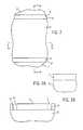
- FIG. 1illustrates a diagrammatic top plan view of a portion of a substrate at a preliminary processing stage according to some embodiments of the present disclosure, showing the substrate with trenches.
- FIG. 1Ais an elevational, cross-sectional view of the substrate depicted in FIG. 1 taken along lines 1 A- 1 A.
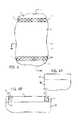
- FIGS. 2-5illustrate diagrammatic top plan views of a portion of a substrate at various stages of processing according to an embodiment of the present disclosure to provide hydrophilic trench ends.
- FIGS. 2A-5A and 2 B- 5 Billustrate elevational, cross-sectional views of the substrate shown in FIGS. 2-5 taken along lines 2 A- 2 A to 5 A- 5 A and lines 2 B- 2 B to 5 B- 5 B, respectively.
- FIG. 6illustrates an elevational, cross-sectional view of a portion of the substrate depicted in FIGS. 1 and 1A at a subsequent processing step according to another embodiment of the disclosure to provide hydrophilic trench ends.
- FIGS. 7 and 8illustrate diagrammatic top plan views of the substrate shown in FIG. 6 in subsequent processing steps.
- FIGS. 7A and 8Aare elevational, cross-sectional views of the substrate shown in FIGS. 7 and 8 taken along lines 7 A- 7 A and 8 A- 8 A, respectively.
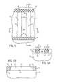
- FIG. 9is an elevational, cross-sectional view of the substrates shown in FIGS. 9A and 9B .
- FIGS. 9A and 9B(taken along lines 9 A/ 9 B- 9 A/ 9 B of FIG. 9 ) are diagrammatic top plan views of the substrates shown, respectively, in FIG. 5 and FIG. 1 at a subsequent processing step, according to different embodiments of the disclosure.
- FIG. 10illustrates an elevational, cross-sectional view of the substrate shown in FIG. 9A at a subsequent processing step.
- FIGS. 11 and 12are diagrammatic top plan views of the substrate of FIG. 10 at subsequent processing stages.
- FIGS. 11A and 12Aare elevational, cross-sectional views of the substrate shown in FIGS. 11 and 12 taken along lines 11 A- 11 A and 12 A- 12 A, respectively.
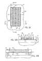
- FIG. 13illustrates a diagrammatic top plan view of a portion of a substrate at a preliminary processing stage according to another embodiment of the present disclosure.
- FIGS. 13A and 13Bare elevational, cross-sectional views of the substrate depicted in FIG. 13 taken along lines 13 A- 13 A and 13 B- 13 B, respectively.
- FIG. 14is a diagrammatic top plan view of the substrate shown in FIG. 13 at a subsequent processing stage.
- FIGS. 14A and 14Bare elevational, cross-sectional views of the substrate shown in FIG. 14 , taken along lines 14 A- 14 A and 14 B- 14 B, respectively.
- FIG. 14Cis an elevational, cross-sectional view of the another embodiment of the substrate shown in FIG. 14 , taken along lines 14 C- 14 C.
- FIG. 15illustrates an elevational, cross-sectional view of the substrate shown in FIG. 14A , at a subsequent processing step.
- FIGS. 16 and 17illustrate a diagrammatic top plan view of the substrate shown in FIG. 15 at subsequent processing stages.
- FIGS. 16A and 17A and 16 B and 17 Bare elevational, cross-sectional views of the substrate shown in FIGS. 16 and 17 taken, respectively, along line 16 A- 16 A, line 17 A- 17 A, line 16 B- 16 B, and line 17 B- 17 B.
- FIGS. 18A and 18Bare elevational, cross-sectional views of the substrate shown in FIG. 17 taken, respectively, along line 18 A- 18 A and line 18 B- 18 B, at a subsequent processing stage.
- FIG. 19is an elevational, cross-sectional view of the substrate shown in FIG. 18A at a subsequent processing stage.
- FIGS. 20-24are elevational, cross-sectional views of the substrate shown in FIG. 5B at subsequent processing stages according to another embodiment of the present disclosure.
- semiconductor substrateor “semiconductive substrate” or “semiconductive wafer fragment” or “wafer fragment” or “wafer” will be understood to mean any construction comprising semiconductor material, including, but not limited to, bulk semiconductive materials such as a semiconductor wafer (either alone or in assemblies comprising other materials thereon) and semiconductive material layers (either alone or in assemblies comprising other materials).
- substraterefers to any supporting structure including, but not limited to, the semiconductive substrates, wafer fragments, or wafers described above.
- “L o ”is the inherent pitch (bulk period or repeat unit) of structures that self assemble upon annealing from a self-assembling (SA) block copolymer or a blend of a block copolymer with one or more of its constituent homopolymers.
- SAself-assembling
- Haldrogelsare cross-linked soluble polymers that swell because of an affinity for water but do not dissolve in water due to structural and/or chemical crosslinks.
- the methodsovercome limitations of fabricating films from self-assembling block copolymers.
- the methodsutilize a trench template defined either lithographically or by use of a film template formed by the graphoepitaxial self-assembly of a lamellar block copolymer inside a wider trench and selective removal of one of the assembled blocks to form films that can be utilized, for example, in etching sub-10 nm features in a substrate.
- FIGS. 1-12Steps in a method for fabricating nanoscale microstructures and microchannels according to an embodiment of the invention are illustrated in FIGS. 1-12 .
- a substrate 10 with an overlying material layer 12is shown.
- the material layer 12is patterned to form trenches 14 .
- the trenches 14can be formed using a lithographic technique such as photolithography, extreme ultraviolet (EUV) lithography, proximity X-rays, electron beam (e-beam) lithography, as known and used in the art.
- EUVextreme ultraviolet
- e-beamelectron beam
- Conventional photolithographycan provide trenches 14 with widths down to about 60 nm.
- E-beam and EUV lithographycan produce smaller features, although at a slower rate and higher expense.
- a method called “pitch doubling” or “pitch multiplication”can also be used for extending the capabilities of photolithographic techniques beyond their minimum pitch, as described, for example, in U.S. Pat. No. 5,328,810 (Lowrey et al.), U.S. Patent Publication No. 2006/0281266 (Wells), and U.S. Patent Publication No. 2007/0023805 (Wells et al.), the disclosures of which are incorporated by reference herein.
- a pattern of linesis photolithographically formed in a photoresist layer overlying a layer of an expendable material, which in turn overlies a substrate.
- the expendable material layeris etched to form placeholders or mandrels.
- the photoresistis stripped. Spacers are formed on the sides of the mandrels, and the mandrels are then removed, leaving behind the spacers as a mask for patterning the substrate.
- the initial photolithographyformed a pattern defining one feature and one space
- the same widthnow defines two features and two spaces, with the spaces defined by the spacers.
- the smallest feature size possible with a photolithographic techniqueis effectively decreased down to about 30 nm or more.
- trenches or grooves with widths in the about 10 nm to 30 nm rangecan be defined using techniques involving graphoepitaxial self-assembly of lamellar-phase block copolymers to provide an etch mask for patterning underlying substrate stacks, e.g., silicon over silicon oxide, as described with reference to FIGS. 13-19 .
- each trench 14is structured with opposing sidewalls 16 , opposing ends 18 (which may also be referred to herein as edges), a floor 20 (which may also be referred to herein as a bottom surface), a width (w t ), a length (l t ), and a depth (D t ).
- the trench dimensionis about 20-200 nm wide (w t ) and about 1600-2400 nm in length (l t ), with a depth (D t ) of about 50-500 nm.
- Substrate 10is exposed as the floor 20 of the trench 14 , and a portion of the material layer 12 forms a spacer interval or crest 12 a between the trenches 14 .
- the trenches 14are structured such that the sidewalls 16 are hydrophobic and preferential wetting to the surfactant component of the described polymer/surfactant emulsion, and the floor 20 of the trench 14 is hydrophilic such that the polymer component will assemble within the center of the trench 14 .
- the substrate 10is composed of an oxide layer (e.g., silicon oxide, SiO x , and the material layer 12 is a silicon layer (with native oxide). Hydrophobic trench sidewalls 16 and ends 18 can be provided by removing the native oxide from the surface of a silicon material layer 12 within the trenches 14 to form hydrogen-terminated silicon.
- oxide layere.g., silicon oxide, SiO x
- silicon layer 12is a silicon layer (with native oxide).
- Hydrophobic trench sidewalls 16 and ends 18can be provided by removing the native oxide from the surface of a silicon material layer 12 within the trenches 14 to form hydrogen-terminated silicon.
- H-terminated siliconcan be prepared by a conventional process, for example, by a fluoride ion etch of silicon (with native oxide present), for example, by immersion in an aqueous solution of hydrogen fluoride (HF) or buffered HF and/or ammonium fluoride (NH 4 F), by HF vapor treatment, by exposure to hot H 2 vapor, or by a hydrogen plasma treatment (e.g., atomic hydrogen).
- a fluoride ion etch of siliconwith native oxide present
- HFhydrogen fluoride
- NH 4 Fbuffered HF and/or ammonium fluoride
- the material layer 12can be composed of a carbonaceous film such as amorphous carbon, which is semi-graphitic but not crystalline in nature, to provide hydrophobic trench sidewalls 16 and ends 18 .
- the amorphous carboncan be a form of transparent carbon that is highly transparent to light. Deposition techniques for forming a highly transparent carbon can be found in A. Helmbold & D.
- amorphous carbon layerscan be formed by chemical vapor deposition using a hydrocarbon compound, or mixtures of such compounds, as carbon precursors such as ethylene, propylene, toluene, propyne, propane, butane, butylene, butadiene, and acetylene.
- a suitable method for forming amorphous carbon layersis described in U.S. Pat. No. 6,573,030 (Fairbairn et al.), the entire disclosure of which is incorporated herein by reference.
- the trench floors 20can then be treated to provide a selectively graftable surface.
- a ligand (anchor, linker) having a reactive moietye.g., an end group
- a reactive moietye.g., an end group
- an example of a useful linker or ligandis poly(ethylene glycol) (PEG) functionalized with an alkyne group, as described, for example, in Michael Malkoch et al., Synthesis of Well - Defined Hydrogel Networks Using Click Chemistry, C HEM . C OMMC'NS 2774-76 (2006), the disclosure of which is incorporated herein by reference.
- PEGpoly(ethylene glycol)
- anhydridee.g., 4-pentynoic anhydride
- PEGcan be reacted with an anhydride in an about 1:1 ratio to derivatize one end of the PEG moiety with an alkyne group and the other end with a hydroxyl group.
- the mono-hydroxylated PEG ligandscan then be grafted to an oxide (e.g., Sift) surface by spin-coating (e.g., from a 1% w/v solution in toluene) and heating to allow the terminal OH groups to diffuse to and react with the oxide layer, as described, for example, in P.
- the PEG group of the attached ligandprovides a linker to the PEG or PEO moieties from the hydrogel emulsion.
- Non-grafted materialcan be removed by rinsing with an appropriate solvent (e.g., toluene).
- an alkyne-functionalized PEG ligand containing a silane group such as trichlorosilane or trialkoxysilanecan be grafted to an oxide surface.
- a mono-hydroxylated PEG ligandcan be reacted with tetrachlorosilane (SiCl 4 ) or tetraethoxysilane Si(OC 2 H 5 ) 4 to produce the desired compound, which can be applied to the trench floors 20 , for example, by spin-on application.
- an example of a suitable linkeris PEG polymer functionalized with an acrylate group at one end such as a PEG acrylate, or PEG methacrylate, which can be obtained from a commercial source such as Sigma-Aldrich Co. (St. Louis, Mo.).
- the surface of both the trench floor 20 and the trench ends 18can be treated to be hydrophilic such that aqueous phase of the emulsion wets both the trench floor 20 and ends 18 , and the surfactant layer (e.g., surfactant monolayer 24 ( FIGS. 9-11A )) forms solely along the hydrophobic trench sidewalls 16 , as in FIGS. 9 and 9A .
- the material layer 12can be structured to provide a silicon surface exposed at the sidewalls 16 that is treated to remove native oxide to form H-terminated silicon and to provide an oxide surface exposed at the ends (edges) 18 (and floor 20 ) of the trenches 14 that is treated with a PEG ligand.
- a material layer 12 of siliconcan be deposited and etched lithographically to form trenches 11 that expose an underlying SiO x layer of the substrate 10 .
- a SiO x layer 13can be deposited to overfill the trenches 11 and removed, for example by chemical-mechanical planarization (CMP), to expose the surface of the silicon material layer 12 and SiO x layer 13 within the trenches 11 , as shown in FIGS. 4-4B .
- CMPchemical-mechanical planarization
- the silicon material layer 12can then be etched lithographically using a photoresist mask to define the trenches 14 with the SiO x layer of the substrate 10 exposed as the trench floor 20 , the SiO x layer 13 as the trench ends 18 , and the silicon material layer 12 exposed as the sidewalls 16 .
- a silicon layer 12 ′can be deposited and etched lithographically to form trenches 14 ′ that expose an underlying SiO x layer 10 ′ (as trenches 14 expose the substrate 10 in FIGS. 1 and 1A ). Then, as illustrated in FIG. 6 , a SiO x layer 13 ′ can be deposited to overfill the trenches 14 ′ and removed, for example, by chemical-mechanical planarization (CMP), to expose the surface of the silicon layer 12 ′ and SiO x layer 13 ′ within the trenches 14 ′, as shown in FIGS. 7 and 7A . As depicted in FIGS.
- CMPchemical-mechanical planarization
- portions of the SiO x layer 13 ′can then be etched lithographically using a photoresist mask to redefine the trenches 14 ′ with the SiO x layer 10 ′ exposed as the trench floor 20 ′, the SiO x layer 13 ′ as the trench ends 18 ′, and the silicon layer 12 ′ exposed as the sidewalls 16 ′.
- an aqueous fluoride treatmentcan be briefly conducted to remove native oxide on the material layer 12 ( FIGS. 5-5B ) or silicon layer 12 ′ ( FIGS. 8 and 8A ) (to form H-terminated silicon sidewalls 16 , 16 ′) while minimizing etching of the SiO x layers (i.e., SiO x layer of substrate 10 , Sift layer 10 ′, and SiO x layer 13 , 13 ′).
- a PEG coupling agentcan then be applied and bound to hydroxyl (—OH) groups on the SiO x floor 20 , 20 ′ and ends 18 , 18 ′ of the trenches 14 , 14 ′ in an inert atmosphere (e.g., nitrogen, argon, etc.) to minimize the reformation of native oxide on the silicon sidewalls 16 , 16 ′.
- an inert atmospheree.g., nitrogen, argon, etc.
- an aqueous emulsion layer 22composed of an amphiphilic agent (e.g., surfactant) and a water-soluble, hydrogel-forming polymer, with optional additives, is applied to fill the trenches 14 and over the material layer 12 (and SiO x layer 13 ).
- the polymer/surfactant emulsion (of the aqueous emulsion layer 22 )can be applied, for example, by casting, dip coating, spray coating, knife-edge coating, spin casting (spin-coating), and the like, such that the aqueous emulsion layer 22 is maintained in a liquid consistency to allow the hydrogel to set up and the surfactant monolayer 24 to form at the trench sidewalls 16 .
- Application of the emulsioncan be conducted at about room temperature (e.g., about 20-25° C.) to up to about 95° C.
- the surfactant componentUpon application of the emulsion, the surfactant component will self-assemble to form a surfactant monolayer 24 (SAM) along the hydrophobic trench surfaces, with a thickness of about 10 nm or less, typically about 3-10 nm, or about 3 nm.
- SAMsurfactant monolayer 24
- the establishment of the surfactant monolayer 24 at the hydrophobic trench sidewalls 16is dependent, at least in part, on the presence of water.
- the aqueous phase 26 of the emulsion comprising the polymer componentorients to the hydrophilic floors 20 at the center of the trenches 14 .
- the rate of self-assembly of the surfactant monolayer 24is relatively rapid at about 0.1-1 minute (or less), and is generally limited by the rate of diffusion of the surfactant to the hydrophobic surfaces (e.g., sidewalls 16 ).
- the formation of the surfactant monolayer 24will occur solely along the trench sidewalls 16 with the polymer aqueous phase 26 of the emulsion wetting the trench floor 20 and ends 18 .
- the surfactant component of the emulsionwill form a surfactant monolayer 24 on both the trench ends 18 and sidewalls 16 , as shown in FIG. 9B .
- Suitable water-soluble and hydrogel-forming polymersinclude, for example, poly(ethylene oxide) (PEO) and poly(ethylene glycol) (PEG).
- PEOpoly(ethylene oxide)
- PEGpoly(ethylene glycol)
- An example of a PEG-based hydrogel materialis described in Michael Malkoch et al., Synthesis of Well - Defined Hydrogel Networks Using Click Chemistry, C HEM . C OMMC'NS 2774-76 (2006), the disclosure of which is incorporated by reference herein.
- a PEG-based hydrogel materialcan be prepared using Click chemistry, e.g., a copper-catalyzed cycloaddition with azide/acetylene coupling reactions, by reacting diacetylene-functionalized and tetraazide-functionalized PEG derivatives at room temperature under aqueous conditions in the presence of copper sulfate (CuSO 4 ) and sodium ascorbate as a reducing agent; wherein a hydrogel can form in less than about 30 minutes at about room temperature.
- Click chemistrye.g., a copper-catalyzed cycloaddition with azide/acetylene coupling reactions, by reacting diacetylene-functionalized and tetraazide-functionalized PEG derivatives at room temperature under aqueous conditions in the presence of copper sulfate (CuSO 4 ) and sodium ascorbate as a reducing agent; wherein a hydrogel can form in less than about 30 minutes at about room temperature.
- the hydrogelcan be synthesized by the photopolymerization of water-soluble vinyl monomers using visible or UV irradiation to form water-soluble polymers with two or more reactive groups, as described, for example, by Kytai Truong Nguyen & Jennifer L. West, Photopolymerizable Hydrogels for Tissue Engineering Applications, 23 (22) B IOMATERIALS 4307-14 (2002), the disclosure of which is incorporated by reference herein.
- photopolymerizable macromersinclude the following: PEG acrylate derivatives (e.g., Amarpreet S.
- the hydrogelcan be synthesized by the free radical-induced crosslinking of PEG-diacrylates or PVA-diacrylates, as described, for example, by P. Martens and K. S. Anseth, Characterization of Hydrogels Formed from Acrylate Modified Poly ( vinyl alcohol ) Macromers, 41 (21) P OLYMER 7715-22 (2000) (acrylate-modified poly(vinyl alcohol) hydrogels); Sheng Lin-Gibson et al., Structure—Property Relationships of Photopolymerizable Poly ( ethylene glycol ) Dimethacrylate Hydrogels, 38 M ACROMOLECULES 2897-902 (2005) (photopolymerizable PEG dimethacrylate hydrogels); Kai Guo & C.
- the hydrogelcan be synthesized by crosslinking cysteine-based peptides with vinyl sulfone-functionalized multi-armed PEG macromers, as described, for example, by M. P. Lutolf et al., Cell - Responsive Synthetic Hydrogels., 15 (11) A DVANCED M ATERIALS 888-92 (2003) (cell-responsive synthetic hydrogels), the disclosure of which is incorporated by reference herein.
- the hydrogelcan be synthesized from PEG macromers and dendritic peptide crosslinkers, as described, for example, by Michel Wathier et al., Dendritic Macromers as In Situ Polymerizing Biomaterials for Security Cataract Incisions, 126 (40) J. A M . C HEM . S OC'Y 12744-45 (2004) (peptide dendron with terminal cysteine residues mixed with PEG dialdehyde), the disclosure of which is incorporated by reference herein.
- amphiphilic surfactant(exhibits both hydrophilic and lipophilic (hydrophobic) characteristics) that will form a self-assembled monolayer (SAM) on the hydrophobic surfaces of the trench.
- amphiphilic surfactantsinclude, for example, phospholipids (anionic surfactants), such as phosphatidylcholines (PCs), phosphatidylserines (PSs), phosphatidylethanolamines, phosphatidylinositols, phosphatidylglycerols, phosphatidic acids, lysophospholipids, among others.
- PCsdipalmitoyl-PC
- POPC1-palmitoyl-2-oleoyl-PC
- DOPCdioleoyl-PC
- DLiPCdilinoleoyl-PC
- the surfactantis included in the emulsion at a concentration effective to form a surfactant monolayer 24 having a thickness of about 10 nm or less or about 3-10 nm.
- a suitable emulsioncan be formulated with an about 5-15% w/w of the polymer and an about 0.5-5% w/w of the surfactant, based on the total weight of the emulsion.
- the emulsioncan include a crosslinking adjuvant or catalyst/cocatalyst.
- a crosslinking adjuvant or catalyst/cocatalystfor example, in the use of Click chemistry to synthesize a PEG-based hydrogel material, the emulsion can include copper sulfate (e.g., at about 1% w/w) and sodium ascorbate, whereby the emulsion would be directly or about immediately dispensed.
- an appropriate peroxide or photoinitiatorcan be included, and the emulsion layer can be crosslinked by exposure to UV light, focused e-beam, heat, etc., as appropriate to crosslink the polymer to form a hydrogel.
- the emulsioncan include a compatible organic solvent to modify the thickness of the surfactant layer over a range of about 3 nm to up to about 10 nm.
- suitable solventsinclude, for example, C 8 -C 24 alkanes (e.g., octane, nonane, decane, undecane, dodecane, etc.), cycloalkanes (e.g., cyclopentane, cyclohexane, etc.), and aromatic hydrocarbons (e.g., benzene, toluene, etc.).
- the emulsioncan optionally include one or more hardening agents to fill or strengthen the hydrogel.
- suitable hardening agentsinclude, for example, inorganic nanoparticles, such as silicon dioxide (SiO 2 ); metal oxides, such as zirconium oxide (ZrO 2 ), titanium dioxide (TiO 2 ), cerium dioxide (CeO 2 ), aluminum oxide, Al 2 O 3 ), iron oxide, vanadia, and tin oxide; carbonates, such as calcium carbonate; and carbon black. Solvated metals that can be precipitated can also be used as hardening agents.
- solvated metalsthat can be used as hardening agents are described, for example, in Joseph Mindel and Cecil V. King, A Study of Bredig Platinum Sols, 65 (11) J. AM . C HEM . S OC'Y 2112-15 (1943) (using electrochemical reduction of metals under water to produce sols of Pb, Sn, Au, Pt, Bi, Sb, As, Tl, Ag, and Hg), the disclosure of which is incorporated by reference herein.
- a silicon estersuch as tetraethoxysilane or tetraethyl orthosilicate (TEOS, Si(OC 2 H 5 ) 4 ) (either neat or as solution in organic solvent or water), can be applied and allowed to diffuse into the hydrogel of the aqueous phase 26 to form a silicon oxide gel via conventional sol-gel reaction to fill in the shape of the hydrogel with an inelastic material.
- TEOStetraethoxysilane or tetraethyl orthosilicate
- the resulting solacts to fuse or precipitate the separate particles of the hardening agent into a contiguous mass or suspension within the hydrogel to further harden the hydrogel, which can remain partially porous.
- oxide hardening agente.g., SiO 2 , TiO 2 , etc.
- the surfactant monolayer 24can be formed as described in U.S. Pat. No. 6,884,842 (Soane et al.), the entire disclosure of which is incorporated by reference herein. Briefly, surfactant monomers containing olefinic group(s), with surface functional head groups that are complementary to a substrate surface, are applied to and self-assemble at a micelle-like interface on the substrate. The positions of the functional groups on the substrate are then stabilized by crosslinking reactive groups on the monomers by a free radical polymerization method to form a thin, insoluble polymer network or mat.
- the resulting surfactant monolayer 24has high thermal and solvent stability, is robust against the removal of water, and is not disrupted by organic solvents such as alcohols that are released during formation of a sol.
- the monomers for forming the surfactant monolayer 24are structured with a head group (e.g., alcohols, carboxylic acids, amides, amines, phosphates, sugars, disaccharides, etc.), a crosslinking group (e.g., a free radically polymerizable moiety, such as acrylates, methacrylates, acrylamides, vinyl ethers, epoxides, etc.), and a tail group fabricated and designed to have surfactant functionality.
- a head groupe.g., alcohols, carboxylic acids, amides, amines, phosphates, sugars, disaccharides, etc.
- a crosslinking groupe.g., a free radically polymerizable moiety, such as acrylates,
- Examples of compoundsinclude acryloylated sulfosuccinic acid ester surfactants, such as (bis(11-acryloylundecyl)sulfosuccinate), (bis-(3-acryloyl-2-ethylhexyl)sulfosuccinate), and (bis-2-acryloyldodecyl sulfosuccinate); and hydroxybenzoic acids, such as glycine-headed-tris(1′-acryloyloxyundecyloxy)benzamide and ethanolamine-headed-tris(11-acryloyloxyundecyloxy)benzamide, which can be prepared as described in U.S. Pat. No. 6,884,842 (Soane et al.).
- acryloylated sulfosuccinic acid ester surfactantssuch as (bis(11-acryloylundecyl)sulfosuccinate), (bis-(3-acryloy
- Self-assembly of the monomers to form the surfactant monolayer 24proceeds by surface aggregation of the head groups at the water interface with the tail groups organized on hydrophobic surfaces, such as the hydrophobic trench sidewalls 16 defined in the material layer 12 .
- Polymerization and crosslinking of the monomerscan be accomplished by known reaction methods, including free-radical polymerization, which can include the application of radiation, such as UV light, to accelerate the process.
- Functional groupssuch as acrylates can be polymerized by heat or radiation such as UV light.
- the polymerization of the crosslinking groups along the backbone after self assemblyis conducted.
- crosslinking reactionssuch as ring opening, condensation, group transfer, anionic and cationic polymerization, can optionally be used, Catalysts and/or photo- or thermal-initiators can optionally be used to promote crosslinking.
- crosslinking groupsinclude acrylates, methacrylates, acrylamides, vinyl ethers, epoxides, methacrylamides, vinylbenzenes, ⁇ -methylvinylbenzenes, divinylbenzenes, vinyl ethers, maleic acid derivatives, fumaric acid derivatives, alkenes, dienes, alkynes, substituted dienes, thiols, alcohols, amines, carboxylic acids, carboxylic anhydrides, carboxylic acid halides, aldehydes, ketones, isocyanates, succinimides, carboxylic acid hydrazides, glycidyl ethers, silanes, siloxanes, chlorosilanes, alkoxysilanes, azides, 2′-pyridyldithiols, phenylglyoxals, iodos, maleimides, aryl halides, imidoesters, dibromopropionate
- the aqueous phase polymer componentis then crosslinked to strengthen and form the robust hydrogel 28 .
- a polymer/surfactant emulsion containing such surfactants and the hydrogel-forming precursorswould be coated onto the substrate 10 , and the hydrogel and surfactant crosslinking can occur about simultaneously or sequentially.
- crosslinkingcan be achieved by applying a catalyst and/or co-catalyst onto the surface of the aqueous emulsion layer 22 , for example, by spraying or applying drops of a catalyst/co-catalyst solution.
- a catalyst/co-catalyst solution of copper sulfate (CuSO 4 ) and sodium ascorbatecan be applied at about room temperature or higher. Further hardening can be applied as needed to produce a structure such as the robust hydrogel 28 ( FIG. 12A ) that is a robust mask for later etching.
- Excess materialcan then be removed, as shown in FIGS. 11 and 11A , to expose the surfactant monolayer 24 (SAM) along the trench sidewalls 16 (and ends 18 , referring to the embodiment in FIG. 9B ). Removal of the excess material can be conducted, for example, using a mechanical planarization apparatus, such as a grinder. Planarization can also be performed using a chemical-mechanical planarization (CMP) apparatus with an alkaline slurry containing abrasive particles, for example, an alkaline silica or ceria slurry with potassium hydroxide (KOH), sodium hydroxide (NaOH), tetramethyl ammonium hydroxide (TMAH; (CH 3 ) 4 NOH), and the like.
- CMPchemical-mechanical planarization
- Removal of the materialcan also be performed using an etch back process, such as a wet etch process (e.g., using basic conditions to remove a PEG hydrogel), or a dry etch (e.g., plasma etch) process to etch the hydrogel (and optionally included hardening agent), for example, a combination of oxygen for the carbonaceous components and a fluorocarbon for silica hardening agents (e.g., CH 2 F 2 , CHF 3 , CF 4 , etc.).
- the hydrogelcan be dried prior to a planarization or etch process to reduce the thickness and facilitate the removal process, provided that the structure of the robust hydrogel 28 has enough structural integrity to not shift during the drying process.
- the surfactant monolayer 24( FIG. 11A ) is then selectively removed leaving a void or channel 30 along the trench sidewalls 16 that is the width of the surfactant monolayer 24 (e.g., up to about 10 nm wide) and the crosslinked, robust hydrogel 28 intact within the center of the trenches 14 .
- selective removal of the surfactant monolayer 24can be achieved, for example, by a wet etch process with an appropriate solvent (e.g., water, alcohols, aromatic hydrocarbons, such as toluene and xylene) or by dry etch.
- a crosslinked surfactant monolayer 24can be removed by a selective dry etch (e.g., plasma etch) process, for example, an oxygen plasma “aching” process, or other appropriate technique.
- the resulting structureis composed of a pair of channels (lines) 30 up to about 10 nm wide (e.g., about 3-10 nm wide) and registered to the trench sidewalls 16 .
- Each pair of channels 30 within a trench 14is separated from each other by the width (w h ) of the hydrogel (e.g., the robust hydrogel 28 ) within the trench 14 , and from a channel 30 in an adjacent trench 14 by the width (Ws) of the spacer 12 a between the trenches 14 .
- the hydrogel film(i.e., the robust hydrogel 28 ) can be then used, for example, as a lithographic template or mask to pattern (arrows ⁇ ) the underlying substrate 10 in a semiconductor processing, for example, by a non-selective RIE etching process, to define a series of channel or grooves 32 (shown in phantom lines in FIG. 12A ) in the sub-10 nanometer size range.
- the grooves 32can then be filled, for example, with a conductive material (e.g., metal) to form nanowire channel arrays for transistor channels, semiconductor capacitors, and to form nanowire channel arrays for transistor gates and digit lines.
- the grooves 32may be filled with a dielectric material to define source/drain active areas. Further processing can then be performed as desired.
- Another method according to an embodiment of the inventionutilizes a graphoepitaxy technique that involves the use of a lithographical-defined (first) trench to direct a lamellar-phase block copolymer film to self assemble into a lamellar array of alternating perpendicular-oriented polymer-rich blocks that extend the length and are ordered and registered to the sidewalls of the (first) trench.
- Selective removal of one of the blocksforms a series of about 10-30 nanometer-scale parallel lines that can be used as a template or mask to etch about 10-30 nm grooves (second trenches) into the underlying substrate within the wider first trench.
- the above-described polymer/surfactant emulsioncan then be formed within the second trenches and processed to form the hydrogel mask to etch a series of sub-10 nanometer-scale grooves in the underlying material layer.
- the surfaces of the sidewalls and ends of the trenchare preferential wetting by the one block of the copolymer and the trench floor is neutral wetting (equal affinity for both blocks of the copolymer) to allow both blocks of the copolymer material to wet the floor of the trench.
- Entropic forcesdrive the wetting of a neutral wetting surface by both blocks, resulting in the formation of a single layer of lamellae across the width of the trench.
- the second trenchesare structured with hydrophilic floors and ends, such that the aqueous phase of the emulsion wets both of those surfaces, and hydrophobic sidewalls, such that the surfactant layer forms solely along that surface (as in FIG. 9 ).
- a substrate 10 ′′is provided bearing a neutral wetting layer 36 ′′ having a neutral wetting surface.
- the substrate 10 ′′can comprise, for example, silicon or amorphous (transparent) carbon or a metal film (e.g., gold, aluminum, etc.).
- the substrate 10 ′′overlies a sub-material layer 34 ′′, which, in some embodiments, comprises an oxide (e.g., silicon oxide, SiO x ), which is inherently hydrophilic.
- a silicon layer in the substrate 10 ′′has been etched lithographically to form trenches 11 ′′ to the underlying sub-SiO x , layer (i.e., sub-material layer 34 ′′, and the trenches 11 ′′ filled with a SiO x layer 13 ′′, as described with reference to FIGS. 2-4B .
- the neutral wetting surface 36 ′′is formed on the substrate 10 ′′ prior to forming the overlying material layer 12 ′′. As illustrated in FIGS. 14-14B , etching through the material layer 12 ′′ to form a first trench 38 ′′ exposes the underlying neutral wetting surface 36 ′′ as the floor or bottom surface 40 ′′ of the trench 38 ′′.
- the neutral wetting surfacecan be provided, for example, by applying a neutral wetting polymer to form a neutral wetting layer 36 ′′ on the surface of the substrate 10 ′′.
- a neutral wetting polymerto form a neutral wetting layer 36 ′′ on the surface of the substrate 10 ′′.
- a neutral wetting polymerto form a neutral wetting layer 36 ′′ on the surface of the substrate 10 ′′.
- a self-assembling (SA) diblock copolymer composed of PS-b-PMMAa random PS:PMMA copolymer brush layer (PS-r-PMMA)) that exhibits non-preferential or neutral wetting toward PS and PMMA can be applied by spin-coating onto the surface of substrate 10 ′′.
- the brushcan be affixed by grafting (on an oxide substrate or native oxide layer) or by crosslinking (any surface) using UV radiation or thermal processing.
- a random copolymer solution composed of PS and PMMA with hydroxyl end groups(e.g., about 58% PS) can be applied to the surface of the substrate 10 ′′ as a layer about 5-10 nm thick and end-grafted by heating at about 160° C. for about 48 hours.
- a trench floor that is neutral wetting to PS-b-PMMAcan also be prepared by spin coating a photo- or thermally-cross-linkable random copolymer, such as benzocyclobutene- or azidomethylstyrene-functionalized random copolymers of styrene and methyl methacrylate (e.g., poly(styrene-r-benzocyclobutene-r-methyl methacrylate) (P(S-r-BCB-r-MMA))), onto the surface of the substrate 10 ′′ and thermally crosslinking the polymer (e.g., at about 200° C. for about 4 hours) to form a cross-linked polymer mat as a neutral wetting layer 36 ′′.
- a photo- or thermally-cross-linkable random copolymersuch as benzocyclobutene- or azidomethylstyrene-functionalized random copolymers of styrene and methyl methacrylate (e.g., poly
- Another neutral wetting surface for PS-b-PMMAcan be provided by hydrogen-terminated silicon, which can be prepared by a conventional process, for example, by a fluoride ion etch of a silicon substrate 10 ′′ (with native oxide present, about 12-15 A), for example, by immersion in aqueous solution of hydrogen fluoride (HF) and buffered HF or ammonium fluoride (NH 4 F), by HF vapor treatment, by exposure to hot H 2 vapor, or by a hydrogen plasma treatment (e.g., atomic hydrogen).
- HFhydrogen fluoride
- NH 4 Fbuffered HF or ammonium fluoride
- the material layer 12 ′′can be formed on the substrate 10 ′′ and etched to form the first trench 38 ′′, and a neutral wetting material for the neutral wetting layer 36 ′′ then applied to the trench floor 40 ′′.
- a cross-linkable random copolymercan be spin coated onto the surface of the substrate 10 ′′ within the first trench 38 ′′ and crosslinked to form a crosslinked polymer mat as the neutral wetting layer 36 ′′. Capillary forces pull the random copolymer to the bottom of the first trench 38 ′′. Non-crosslinked polymer material can be subsequently removed.
- a neutral-wetting polymersuch as random copolymer of P(S-r-MMA-r-HEMA)
- NWPneutral-wetting polymer
- a material layere.g., an oxide floor.
- an olefinic monomersuch as PMMA or PS
- a di-olefinic linkersuch as divinyl benzene
- a material layer 12 ′′is formed on the substrate 10 ′′ and patterned to form the first trench 38 ′′ structured with a floor or bottom surface 40 ′′, opposing sidewalls 42 ′′, opposing ends (edges) 44 ′′, a width (w), a length (l) and a depth (D).
- the first trench 38 ′′can be formed by a lithographic technique, for example, photolithography, extreme ultraviolet (EUV) lithography, proximity X-rays, and electron beam (e-beam) lithography, as known and used in the art.
- EUVextreme ultraviolet
- e-beamelectron beam
- the trench sidewalls 42 ′′ and ends 44 ′′are preferential wetting by one block of the copolymer to induce formation of lamellar polymer domains as the blocks self-assemble.
- the material layer 12 ′′ defining the trench surfacescan be an inherently preferential wetting material, or in other embodiments, a layer of a preferential wetting material can be applied onto the surfaces of the first trench 38 ′′.
- the material layer 12 ′′can be composed of an oxide (e.g., silicon oxide, SiO x ) or a clean silicon surface (with native silicon oxide), which exhibits preferential wetting toward the PMMA block to result in the assembly of a thin (e.g., 1 ⁇ 4 pitch) interface layer of PMMA and alternating PMMA and PS lamellae (e.g., 1 ⁇ 2 pitch) within the first trench 38 ′′ in the use of a lamellar-phase block copolymer material.
- an oxidee.g., silicon oxide, SiO x
- a clean silicon surfacewith native silicon oxide
- PMMApolymethylmethacrylate
- a PMMA that is modified with a moiety containing one or more hydroxyl (—OH) groupscan be applied by spin-coating and then heated (e.g., to about 170° C.) to allow the OH groups to end-graft to the oxide sidewalls 42 ′′ and ends 44 ′′ of the first trench 38 ′′.
- Non-grafted materialcan be removed from the neutral wetting layer 36 ′′ by rinsing with an appropriate solvent (e.g., toluene).
- an appropriate solvente.g., toluene
- P. Mansky et al.Controlling Polymer - Surface Interactions with Random Copolymer Brushes, 275 (5305) S CIENCE 1458-60 (1997), and Insik In et al., Side - Chain - Grafted Random Copolymer Brushes as Neutral Surfaces for Controlling the Orientation of Block Copolymer Microdomains in Thin Films, 22 L ANGMUIR 7855-60 (2006), the disclosures of each of which are incorporated by reference herein.
- the trench sidewalls 42 ′′, ends 44 ′′, and floor 40 ′′influence the structuring of the array of lamellae within the first trench 38 ′′.
- the boundary conditions of the trench sidewalls 42 ′′ in both the x- and y-axisimpose a structure such that the first trench 38 ′′ contains n number of lamellae.
- Factors in forming a single array or layer of lamellae within the first trench 38 ′′include the width and depth of the first trench 38 ′′, the formulation of the block copolymer to achieve the desired pitch (L o ), and the thickness (t) ( FIG. 15 ) of the copolymer film.
- the first trench 38 ′′is constructed with a width (w) such that a lamellar-forming block copolymer (or blend) will self assemble upon annealing into a single layer of “n” lamellae spanning the width (w) of the first trench 38 ′′, with each lamellar domain being separated by a value of L o (from center-to-center).
- the width (w) of the first trench 38 ′′is a multiple of the inherent pitch value (L o ) of the block copolymer being equal to or about nL o (“n*L o ”), typically ranging from about n*10 to about n*100 nm (with n being the number of features or structures).
- the depth (D) of the first trench 38 ′′is greater than or at about L o , as illustrated in FIG. 14A .
- the application and annealing of a block copolymer material having an inherent pitch value of L o in a first trench 38 ′′ having a width (w) at or about L owill result in the formation of a single layer of “n” lamellae spanning the width (w) and registered to the sidewalls 42 ′′ for the length of the first trench 38 ′′.
- the dimensions of the first trench 38 ′′are about 55-80 nm wide (w) and about 1600-2400 ⁇ m in length (l), with a depth (D) of about 50-500 nm.
- a layer 46 ′′ of a lamellar-phase self-assembling (SA) block copolymer material having an inherent pitch at or about L o (or a ternary blend of block copolymer and homopolymers blended to have a pitch at or about L o )is then deposited, typically by spin casting (spin-coating), onto the floor 40 ′′ of the first trench 38 ′′.
- the block copolymer materialcan be deposited onto the patterned surface by spin casting from a dilute solution (e.g., about 0.25-2 wt % solution) of the copolymer in an organic solvent, such as dichloroethane (CH 2 Cl 2 ) or toluene, for example.
- the lamellar-phase block copolymer materialis deposited into the first trench 38 ′′ to a thickness (t) less than the trench depth (D), for example, at about one-half of the trench depth (D), and at or about the L o value of the block copolymer material such that the copolymer film layer will self assemble upon annealing to form a single layer of lamellae across the width (w t ) of the first trench 38 ′′.
- a typical thickness (1) of the block copolymer filmis about ⁇ 20% of the L o value of the polymer (e.g., about 10-100 nm) to form alternating polymer-rich lamellar blocks, each with a width of about L o (e.g., 25-35 nm) across the width (w) of the first trench 38 ′′.
- the thickness (t) of the layer 46 ′′can be measured, for example, by ellipsometry techniques. As shown, a thin film of less than L o of the block copolymer material can be deposited onto the surface of the material layer 12 ′′; this thin film will not self-assemble as it is not thick enough to form structures.
- the volume fractions of the two blocks (AB) of the lamellar-forming diblock copolymerare generally at a ratio between about 50:50 and 60:40.
- An example of a lamellae-forming symmetric diblock copolymeris poly(styrene-block-methyl methacrylate) (PS-b-PMMA), with a weight ratio of about 50:50 (PS:PMMA) and total molecular weight (M n ) of about 51 kg/mol.
- diblock copolymersare used in the illustrative embodiments, other types of block copolymers (i.e., triblock or multiblock copolymers) can be used.
- diblock copolymersinclude poly(styrene-block-methyl methacrylate) (PS-b-PMMA), polyethyleneoxide-polyisoprene, polyethyleneoxide-polybutadiene, polyethyleneoxide-polystyrene, polyethyleneoxide-polymethylmethacrylate, polystyrene-polyvinylpyridine, polystyrene-polyisoprene (PS-b-PI), polystyrene-polybutadiene, polybutadiene-polyvinylpyridine, and polyisoprene-polymethylmethacrylate, among others.
- PS-b-PMMApoly(styrene-block-methyl methacrylate)
- PS-b-PMMApolyethyleneoxide-polyiso
- triblock copolymersexamples include poly(styrene-block methyl methacrylate-block-ethylene oxide).
- One of the polymer blocks of the block copolymershould be selectively and readily removable in order to fabricate an etch mask or template from the annealed film.
- the block copolymer materialcan also be formulated as a binary or ternary blend comprising a SA block copolymer and one or more homopolymers of the same type of polymers as the polymer blocks in the block copolymer, to produce blends that swell the size of the polymer domains and increase the L o value of the polymer.
- the volume fraction of the homopolymerscan range from 0% to about 40%.
- An example of a ternary diblock copolymer blendis a PS-b-PMMA/PS/PMMA blend, for example, 46K/21K PS-b-PMMA containing 40% 20K polystyrene and 20K poly(methylmethacrylate).
- the L o value of the polymercan also be modified by adjusting the molecular weight of the block copolymer, e.g., for lamellae, L o ⁇ (MW) 2/3 .
- the block copolymer film(i.e., layer 46 ′′) is then annealed to form a self-assembled lamellar film 48 ′′, for example, by thermal annealing to above the glass transition temperature of the component blocks of the copolymer material to cause the polymer blocks to separate and self assemble into blocks 50 ′′, 52 ′′ according to the preferential and neutral wetting of the trench surfaces, i.e., floors 40 ′′, sidewalls 42 ′′, and ends 44 ′′.
- a PS-b-PMMA copolymer filmcan be annealed, for example, at about 180-195° C. in a vacuum oven for about 1-170 hours to produce a self-assembled film.
- the self-assembled lamellar film 48 ′′can also be solvent annealed, for example, by slowly swelling both blocks 50 ′′, 52 ′′ of the self-assembled lamellar film 48 ′′ with a solvent, then slowly evaporating the solvent.
- the constraints provided by the width (w) of the first trench 38 ′′ and the character of the block copolymer composition combined with preferential and neutral wetting surfaces within the first trench 38 ′′results, upon annealing, in a single layer of n perpendicular-oriented, alternating lamellar polymer-rich blocks extending the length (l) and spanning the width (w) of the first trench 38 ′′ at an average pitch value of at or about L o (center-to-center).
- the number “n” or pitches of lamellar blocks within the first trench 38 ′′is according to the width (w) of the first trench 38 ′′ and the molecular weight (MW) of the copolymer.
- the perpendicular orientation of lamellaecan be examined, for example, using atomic force microscopy (AFM), transmission electron microscopy (TEM), or scanning electron microscopy (SEM).
- AFMatomic force microscopy
- TEMtransmission electron microscopy
- SEMscanning electron microscopy
- one of the block componentscan be selectively removed to produce a thin film 54 ′′ having registered and parallel oriented openings (slits) 56 ′′ that can be used, for example, as a lithographic template or mask to pattern the underlying substrate 10 ′′ within the first trench 38 ′′ in a semiconductor processing to define regular patterns in the nanometer size range (i.e., about 10-100 nm).
- block 50 ′′e.g., the PMMA domains
- openings (slits) 56 ′′ separated by another of the block components, block 52 ′′e.g., vertically oriented PS lamellar domains
- the trench floor 40 ′′e.g., neutral wetting layer 36 ′′ over substrate 10 ′′
- the first blocks 50 ′′i.e., the PMMA blocks
- Removal of the first blocks 50 ′′can be performed, for example, by application of an oxygen (O 2 ) plasma or CF 4 plasma (e.g., about 3:1 selective for PMMA), or by a chemical dissolution process such as acetic acid sonication by first irradiating the sample (ultraviolet (DV) radiation, 1 J/cm 2 254 nm light), then ultrasonicating the self-assembled lamellar film 48 ′′ in glacial acetic acid, ultrasonicating in deionized water, and rinsing the self-assembled lamellar film 48 ′′ in deionized water to remove the degraded PMMA (i.e., the first blocks 50 ′′).
- O 2oxygen
- CF 4 plasmae.g., about 3:1 selective for PMMA
- acetic acid sonicationby first irradiating the sample (ultraviolet (DV) radiation, 1 J/cm 2 254 nm light), then ultrasonicating the self-assembled
- the resulting thin film 54 ′′will have a corrugated surface that defines a linear pattern of fine, nanometer-scale parallel openings (slits) 56 ′′ about 10-60 nm wide and extending the length of the first trench 38 ′′, the individual openings (slits) 56 ′′separated by a polymer matrix of the second blocks 52 ′′ (e.g., of PS) about 10-60 nm wide.
- a polymer matrix of the second blocks 52 ′′e.g., of PS
- PSi.e., second block 52 ′′
- a smaller pitchcan be dialed in by using lower molecular weight diblock copolymers.
- the thin film 54 ′′can then be used as a lithographic template or etch mask to pattern (arrows ⁇ ) the underlying substrate 10 ′′ (e.g., silicon), for example, by a non-selective RIE etching process, to delineate a series of trenches (grooves, channels) 14 ′′ as illustrated in FIGS. 18A and 18B .
- the residual thin film 54 ′′e.g., polystyrene
- Etching through the substrate 10 ′′ (e.g., silicon) to form the trenches 14 ′′exposes the underlying sub-material layer 34 ′′, which is oxide in the illustrated example, as the floor or bottom surface 20 ′′ of the trenches 14 ′′, the oxide layer (i.e., SiO x layer 13 ′′) as the ends 18 ′′, and substrate 10 ′′/ 10 a ′′, which is silicon in the illustrated example, as the sidewalls 16 ′′.
- the dimensions of the trenches 14 ′′are about 10-60 nm wide (W t ) and about 10-100 nm deep with a depth (D t ).
- an aqueous fluoride treatmentcan be briefly conducted to remove native oxide on the silicon layer of the substrate 10 ′′ (to form H-terminated silicon sidewalls 16 ′′) while minimizing etching of the SiO x layer 13 ′′ and sub-material layer 34 ′′.
- a PEG coupling agentcan then be applied as previously described, for example, by grafting a ligand with a reactive end group such as a mono-hydroxylated PEG ligand to hydroxyl (—OH) groups on the SiO x floor 20 ′′ and ends 18 ′′ of the trenches 14 ′′ in an inert atmosphere (e.g., nitrogen, argon, etc.) to minimize the reformation of native oxide on the silicon sidewalls 16 ′′.
- an inert atmospheree.g., nitrogen, argon, etc.
- the previously described aqueous polymer/surfactant emulsioncan then be applied to fill the trenches 14 ′′ and processed to form an etch mask composed of the hydrogel material to etch the sub-material layer 34 ′′ to form grooves or channels (e.g., 32 shown in phantom lines in FIG. 12A ).
- a substrate 10 ′′′such as the substrate 10 as described with respect to FIGS. 5-5B (or the substrate 10 ′ as described with respect to FIGS. 8 and 8 A) can be prepared having trenches 14 ′′′ with a hydrophilic floor 20 ′′′, hydrophilic ends 18 ′′′ (e.g., of SiO x ), and hydrophobic sidewalls 16 ′′′ (e.g., H-terminated silicon).
- a substrate 10 ′′′such as the substrate 10 as described with respect to FIGS. 5-5B (or the substrate 10 ′ as described with respect to FIGS. 8 and 8 A) can be prepared having trenches 14 ′′′ with a hydrophilic floor 20 ′′′, hydrophilic ends 18 ′′′ (e.g., of SiO x ), and hydrophobic sidewalls 16 ′′′ (e.g., H-terminated silicon).
- an aqueous emulsion(for an aqueous emulsion layer 58 ′′′) composed of a self-assembling amphiphilic agent, e.g., surfactant monomers, for example, as described above with reference to U.S. Pat. No. 6,884,842 (Sloane et al.), containing olefinic group(s) with surface functional head groups that are complementary to a substrate surface, can be applied to fill the trenches 14 ′′′ and over the material layer 12 ′′′.
- a self-assembling amphiphilic agente.g., surfactant monomers, for example, as described above with reference to U.S. Pat. No. 6,884,842 (Sloane et al.)
- olefinic group(s) with surface functional head groupsthat are complementary to a substrate surface
- the emulsioncan be applied, for example, by casting, dip coating, spray coating, knife-edge coating, spin casting (spin-coating), and the like, such that the emulsion layer 58 ′′′ is maintained in a liquid consistency to allow a layer of the amphiphilic agent (e.g., surfactant) to form at the trench hydrophobic sidewalls 16 ′′′.
- Application of the emulsioncan be conducted at about room temperature (e.g., about 20-25° C.) to up to about 95° C.
- the amphiphilic agente.g., surfactant monomers
- the amphiphilic agentwill self-assemble to form a surfactant monolayer 24 ′′′ on the hydrophobic sidewalls 16 ′′′ (e.g., H-terminated silicon) of the trenches 14 ′′′.
- the monomerscan then be polymerized and crosslinked, for example, by free-radical polymerization, to form a robust, thin, insoluble surfactant monolayer from the surfactant monolayer 24 ′′′.
- the robust surfactant monolayer 24 ′′′can then be dried, for example, by heating and/or blow-drying with a dry gas such as nitrogen, argon, and clean dry air, or by a Marangoni drying technique in which the structure is immersed in a DI water bath and drawn through a layer of a water-miscible solvent that is more volatile than water such as isopropyl alcohol (IPA), which rests on the surface of the DI water bath.
- IPAisopropyl alcohol
- Micellar structures or other material that has precipitated onto the trench hydrophilic floor 20 ′′′ and hydrophobic sidewalls 16 ′′′ during crosslinking of the surfactant monomerscan be removed, for example, by rinsing or sonicating using a liquid that does not swell the crosslinked surfactant material or cause dewetting of the surfactant monolayer, for example, water, methanol, and isopropanol.
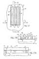
- an inorganic material layer 60 ′′′such as a dielectric material can then be deposited, for example, by a chemical deposition process at a low temperature such that the robust surfactant monolayer 24 ′′′ is not degraded (e.g., below about 150° C.), to fill the trenches 14 ′′′.
- Suitable dielectric materialsinclude, for example, silicon oxide (SiO x ), aluminum oxide (Al 2 O 3 ), tantalum oxide (TaO x ), silicon carbide (SiC), hafnium oxide (HfO 2 ), hafnium aluminum oxide (HfAlO), silicon carbon nitride (SiCN), silicon nitride (SiN 4 ), yttrium oxide (YO 2 ), and tantalum pentoxide (Ta 2 O 5 ). Excess material can then be removed as in FIG. 23 , for example, by mechanical planarization, chemical-mechanical planarization, or an etch back process, to expose the robust surfactant monolayer 24 ′′′ along the trench hydrophobic sidewalls 16 ′′′.
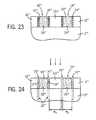
- the surfactant monolayer 24 ′′′ along the trench hydrophobic sidewalls 16 ′′′can then be selectively removed, leaving a channel or gap 30 ′′′ that is the width of the surfactant monolayer 24 ′′′ (e.g., up to about 10 nm wide), with the inorganic material layer 60 ′′′ remaining intact within the center of the trenches 14 ′′′.
- Selective removal of the crosslinked (i.e., robust) surfactant monolayer 24 ′′′can be achieved, for example, by a selective dry etch (e.g., plasma etch) process, for example, an oxygen plasma “ashing” process, or other appropriate technique.
- the resulting structureis composed of a pair of channels (lines) or gaps 30 ′′′ up to about 10 nm wide (e.g., about 3-10 nm wide) and registered to the trench hydrophobic sidewalls 16 ′′′.
- Each pair of channels or gaps 30 ′′′ within a trench 14 ′′′is separated from each other by the width (w x ) of the inorganic material layer 60 ′′′ within the trench 14 ′′′, and from a channel or gap 30 ′′′ in an adjacent trench 14 ′′′ by the width (w s ) of the spacer 12 a ′′′ between the trenches 14 ′′′.
- the inorganic material layer 60 ′′′can be then used, for example, as a lithographic template or mask to pattern (arrows ⁇ ) the underlying substrate 10 ′′′, for example, by a non-selective RIE etching process, to define a series of channels or grooves 32 ′′′ (shown in phantom lines in FIG. 24 ) in the sub-10 nanometer size range, which can be filled with metal or other conductive material, or dielectric material, for example.
- the described filmsare useful as lithographic templates or etch masks for producing close-pitched, ordered, and registered, nanoscale channels and grooves that are sub-10 nm wide and several nanometers in length, for producing features such as floating gates for NAND flash with nanoscale dimensions.
- photolithography techniquesare unable to produce channels much below 60 nm wide without high expense. Resolution can exceed other techniques for forming channels and grooves, including self-assembling block copolymer processing and conventional photolithography. Fabrication costs utilizing methods of the disclosure are far less than electron beam (e-beam) or EUV photolithographies, which have comparable resolution.
Landscapes
- Engineering & Computer Science (AREA)
- Chemical & Material Sciences (AREA)
- Manufacturing & Machinery (AREA)
- Microelectronics & Electronic Packaging (AREA)
- Physics & Mathematics (AREA)
- Condensed Matter Physics & Semiconductors (AREA)
- General Physics & Mathematics (AREA)
- Nanotechnology (AREA)
- Power Engineering (AREA)
- Computer Hardware Design (AREA)
- Materials Engineering (AREA)
- Crystallography & Structural Chemistry (AREA)
- Composite Materials (AREA)
- Analytical Chemistry (AREA)
- Micromachines (AREA)
- Photosensitive Polymer And Photoresist Processing (AREA)
- Treatments Of Macromolecular Shaped Articles (AREA)
- Physical Or Chemical Processes And Apparatus (AREA)
- Application Of Or Painting With Fluid Materials (AREA)
- Compositions Of Macromolecular Compounds (AREA)
- Colloid Chemistry (AREA)
- Processes Of Treating Macromolecular Substances (AREA)
Abstract
Description
- about 5-15% w/w water-soluble, hydrogel-forming polymer;
- about 1-5% w/w amphiphilic surfactant;
- about 0-5% w/w organic solvent;
- about 0-20% w/w (or more) hardening agent;
- about 0-5% w/w cross-linking adjuvants; and
- about 94-55% w/w water.
- In some embodiments, after formation of the hydrogel with the
aqueous phase 26 within thetrenches 14, a liquid filler material can be applied to thesurfactant monolayer 24 and hydrogel of theaqueous phase 26 to reduce the impact of drying on the shape and adherence of thesurfactant monolayer 24 to the hydrophobic trench surfaces and to further strengthen and reduce the porosity of the polymer hydrogel such that the shape of the hydrogel is retained after removal of thesurfactant monolayer 24 and it functions as an adequate mask during a plasma etching process (seeFIG. 12A , element28 (a robust hydrogel28)).
Claims (21)
Priority Applications (2)
| Application Number | Priority Date | Filing Date | Title |
|---|---|---|---|
| US13/473,748US8784974B2 (en) | 2007-03-22 | 2012-05-17 | Sub-10 NM line features via rapid graphoepitaxial self-assembly of amphiphilic monolayers |
| US14/300,404US20140290858A1 (en) | 2007-03-22 | 2014-06-10 | Methods of forming a polymeric material via self-assembly of amphiphilic material and related template structures |
Applications Claiming Priority (2)
| Application Number | Priority Date | Filing Date | Title |
|---|---|---|---|
| US11/726,674US8557128B2 (en) | 2007-03-22 | 2007-03-22 | Sub-10 nm line features via rapid graphoepitaxial self-assembly of amphiphilic monolayers |
| US13/473,748US8784974B2 (en) | 2007-03-22 | 2012-05-17 | Sub-10 NM line features via rapid graphoepitaxial self-assembly of amphiphilic monolayers |
Related Parent Applications (2)
| Application Number | Title | Priority Date | Filing Date |
|---|---|---|---|
| US11/726,674ContinuationUS8557128B2 (en) | 2007-03-22 | 2007-03-22 | Sub-10 nm line features via rapid graphoepitaxial self-assembly of amphiphilic monolayers |
| US11/726,674DivisionUS8557128B2 (en) | 2007-03-22 | 2007-03-22 | Sub-10 nm line features via rapid graphoepitaxial self-assembly of amphiphilic monolayers |
Related Child Applications (1)
| Application Number | Title | Priority Date | Filing Date |
|---|---|---|---|
| US14/300,404DivisionUS20140290858A1 (en) | 2007-03-22 | 2014-06-10 | Methods of forming a polymeric material via self-assembly of amphiphilic material and related template structures |
Publications (2)
| Publication Number | Publication Date |
|---|---|
| US20120223051A1 US20120223051A1 (en) | 2012-09-06 |
| US8784974B2true US8784974B2 (en) | 2014-07-22 |
Family
ID=39789232
Family Applications (4)
| Application Number | Title | Priority Date | Filing Date |
|---|---|---|---|
| US11/726,674ActiveUS8557128B2 (en) | 2007-03-22 | 2007-03-22 | Sub-10 nm line features via rapid graphoepitaxial self-assembly of amphiphilic monolayers |
| US12/723,176ActiveUS8801894B2 (en) | 2007-03-22 | 2010-03-12 | Sub-10 NM line features via rapid graphoepitaxial self-assembly of amphiphilic monolayers |
| US13/473,748ActiveUS8784974B2 (en) | 2007-03-22 | 2012-05-17 | Sub-10 NM line features via rapid graphoepitaxial self-assembly of amphiphilic monolayers |
| US14/300,404AbandonedUS20140290858A1 (en) | 2007-03-22 | 2014-06-10 | Methods of forming a polymeric material via self-assembly of amphiphilic material and related template structures |
Family Applications Before (2)
| Application Number | Title | Priority Date | Filing Date |
|---|---|---|---|
| US11/726,674ActiveUS8557128B2 (en) | 2007-03-22 | 2007-03-22 | Sub-10 nm line features via rapid graphoepitaxial self-assembly of amphiphilic monolayers |
| US12/723,176ActiveUS8801894B2 (en) | 2007-03-22 | 2010-03-12 | Sub-10 NM line features via rapid graphoepitaxial self-assembly of amphiphilic monolayers |
Family Applications After (1)
| Application Number | Title | Priority Date | Filing Date |
|---|---|---|---|
| US14/300,404AbandonedUS20140290858A1 (en) | 2007-03-22 | 2014-06-10 | Methods of forming a polymeric material via self-assembly of amphiphilic material and related template structures |
Country Status (3)
| Country | Link |
|---|---|
| US (4) | US8557128B2 (en) |
| TW (1) | TWI390601B (en) |
| WO (1) | WO2008118635A2 (en) |
Cited By (7)
| Publication number | Priority date | Publication date | Assignee | Title |
|---|---|---|---|---|
| US9257256B2 (en) | 2007-06-12 | 2016-02-09 | Micron Technology, Inc. | Templates including self-assembled block copolymer films |
| US9431605B2 (en) | 2011-11-02 | 2016-08-30 | Micron Technology, Inc. | Methods of forming semiconductor device structures |
| US9768021B2 (en) | 2007-04-18 | 2017-09-19 | Micron Technology, Inc. | Methods of forming semiconductor device structures including metal oxide structures |
| US10005308B2 (en) | 2008-02-05 | 2018-06-26 | Micron Technology, Inc. | Stamps and methods of forming a pattern on a substrate |
| US10049874B2 (en) | 2013-09-27 | 2018-08-14 | Micron Technology, Inc. | Self-assembled nanostructures including metal oxides and semiconductor structures comprised thereof |
| US10153200B2 (en) | 2008-03-21 | 2018-12-11 | Micron Technology, Inc. | Methods of forming a nanostructured polymer material including block copolymer materials |
| US11841617B2 (en) | 2019-09-19 | 2023-12-12 | Tokyo Electron Limited | Method of forming a narrow trench |
Families Citing this family (41)
| Publication number | Priority date | Publication date | Assignee | Title |
|---|---|---|---|---|
| US8394483B2 (en) | 2007-01-24 | 2013-03-12 | Micron Technology, Inc. | Two-dimensional arrays of holes with sub-lithographic diameters formed by block copolymer self-assembly |
| US8083953B2 (en) | 2007-03-06 | 2011-12-27 | Micron Technology, Inc. | Registered structure formation via the application of directed thermal energy to diblock copolymer films |
| US8557128B2 (en) | 2007-03-22 | 2013-10-15 | Micron Technology, Inc. | Sub-10 nm line features via rapid graphoepitaxial self-assembly of amphiphilic monolayers |
| US8294139B2 (en) | 2007-06-21 | 2012-10-23 | Micron Technology, Inc. | Multilayer antireflection coatings, structures and devices including the same and methods of making the same |
| US7959975B2 (en) | 2007-04-18 | 2011-06-14 | Micron Technology, Inc. | Methods of patterning a substrate |
| US8372295B2 (en) | 2007-04-20 | 2013-02-12 | Micron Technology, Inc. | Extensions of self-assembled structures to increased dimensions via a “bootstrap” self-templating method |
| US8080615B2 (en) | 2007-06-19 | 2011-12-20 | Micron Technology, Inc. | Crosslinkable graft polymer non-preferentially wetted by polystyrene and polyethylene oxide |
| US7790350B2 (en)* | 2007-07-30 | 2010-09-07 | International Business Machines Corporation | Method and materials for patterning a neutral surface |
| US8215074B2 (en)* | 2008-02-05 | 2012-07-10 | International Business Machines Corporation | Pattern formation employing self-assembled material |
| US8101261B2 (en) | 2008-02-13 | 2012-01-24 | Micron Technology, Inc. | One-dimensional arrays of block copolymer cylinders and applications thereof |
| US7906031B2 (en)* | 2008-02-22 | 2011-03-15 | International Business Machines Corporation | Aligning polymer films |
| US8425982B2 (en) | 2008-03-21 | 2013-04-23 | Micron Technology, Inc. | Methods of improving long range order in self-assembly of block copolymer films with ionic liquids |
| US8114300B2 (en)* | 2008-04-21 | 2012-02-14 | Micron Technology, Inc. | Multi-layer method for formation of registered arrays of cylindrical pores in polymer films |
| US8114301B2 (en) | 2008-05-02 | 2012-02-14 | Micron Technology, Inc. | Graphoepitaxial self-assembly of arrays of downward facing half-cylinders |
| US8822347B2 (en)* | 2009-04-27 | 2014-09-02 | Taiwan Semiconductor Manufacturing Company, Ltd. | Wet soluble lithography |
| FR2950241B1 (en)* | 2009-09-18 | 2011-09-23 | Commissariat Energie Atomique | FANTOME BIOMODALITY OF ORGANS AND METHOD OF MAKING THE SAME |
| CN101717068B (en)* | 2009-11-19 | 2013-04-10 | 复旦大学 | Method for preparing polymeric micro-fluidic chip based on hydrogel male mold |
| US8815747B2 (en)* | 2010-06-03 | 2014-08-26 | Micron Technology, Inc. | Methods of forming patterns on substrates |
| US8304493B2 (en) | 2010-08-20 | 2012-11-06 | Micron Technology, Inc. | Methods of forming block copolymers |
| US9233840B2 (en) | 2010-10-28 | 2016-01-12 | International Business Machines Corporation | Method for improving self-assembled polymer features |
| FR2975823B1 (en)* | 2011-05-27 | 2014-11-21 | Commissariat Energie Atomique | METHOD FOR MAKING A PATTERN ON THE SURFACE OF A BLOCK OF A SUBSTRATE USING BLOCK COPOLYMERS |
| US9449839B2 (en) | 2012-08-06 | 2016-09-20 | Taiwan Semiconductor Manufacturing Co., Ltd. | Self-assembled monolayer for pattern formation |
| US8883646B2 (en)* | 2012-08-06 | 2014-11-11 | Taiwan Semiconductor Manufacturing Co., Ltd. | Self-assembled monolayer for pattern formation |
| US9087699B2 (en) | 2012-10-05 | 2015-07-21 | Micron Technology, Inc. | Methods of forming an array of openings in a substrate, and related methods of forming a semiconductor device structure |
| US9054215B2 (en)* | 2012-12-18 | 2015-06-09 | Intel Corporation | Patterning of vertical nanowire transistor channel and gate with directed self assembly |
| KR101993255B1 (en)* | 2013-01-07 | 2019-06-26 | 삼성전자주식회사 | Method of forming contact holes |
| US8993404B2 (en)* | 2013-01-23 | 2015-03-31 | Intel Corporation | Metal-insulator-metal capacitor formation techniques |
| JP5802233B2 (en) | 2013-03-27 | 2015-10-28 | 株式会社東芝 | Pattern formation method |
| US8853085B1 (en)* | 2013-04-23 | 2014-10-07 | International Business Machines Corporation | Grapho-epitaxy DSA process with dimension control of template pattern |
| US9229328B2 (en) | 2013-05-02 | 2016-01-05 | Micron Technology, Inc. | Methods of forming semiconductor device structures, and related semiconductor device structures |
| US9330914B2 (en) | 2013-10-08 | 2016-05-03 | Micron Technology, Inc. | Methods of forming line patterns in substrates |
| US9190285B1 (en) | 2014-05-06 | 2015-11-17 | International Business Machines Corporation | Rework and stripping of complex patterning layers using chemical mechanical polishing |
| JP6173989B2 (en)* | 2014-08-29 | 2017-08-02 | 東芝メモリ株式会社 | Pattern formation method |
| KR102226116B1 (en)* | 2014-09-12 | 2021-03-11 | 삼성디스플레이 주식회사 | Wire grid polarizer and method for fabricating the same |
| KR102358710B1 (en)* | 2015-04-06 | 2022-02-08 | 에스케이하이닉스 주식회사 | Method of forming different sized patterns |
| WO2017105447A1 (en)* | 2015-12-16 | 2017-06-22 | Intel Corporation | Methods and apparatuses to provide ordered porosity |
| US10056265B2 (en)* | 2016-03-18 | 2018-08-21 | Taiwan Semiconductor Manufacturing Co., Ltd. | Directed self-assembly process with size-restricted guiding patterns |
| US9793132B1 (en)* | 2016-05-13 | 2017-10-17 | Applied Materials, Inc. | Etch mask for hybrid laser scribing and plasma etch wafer singulation process |
| US20180323061A1 (en)* | 2017-05-03 | 2018-11-08 | Tokyo Electron Limited | Self-Aligned Triple Patterning Process Utilizing Organic Spacers |
| US11696688B2 (en)* | 2017-11-17 | 2023-07-11 | Shimadzu Corporation | Semiconductor SWCNT slurry for bioimaging and method for producing the same |
| CN112533395B (en)* | 2020-12-21 | 2021-12-24 | 北京同方信息安全技术股份有限公司 | Method for embedding resistor in printed circuit board and printed circuit board thereof |
Citations (286)
| Publication number | Priority date | Publication date | Assignee | Title |
|---|---|---|---|---|
| US4623674A (en) | 1985-06-21 | 1986-11-18 | Union Carbide Corporation | Polymer/polyols of substituted styrenes and polyurethanes made therefrom |
| US4797357A (en) | 1986-05-30 | 1989-01-10 | Eastman Kodak Company | Light-stable reducible compounds and analytical compositions, elements and methods utilizing same |
| US4818713A (en) | 1987-10-20 | 1989-04-04 | American Telephone And Telegraph Company, At&T Bell Laboratories | Techniques useful in fabricating semiconductor devices having submicron features |
| US4877647A (en) | 1986-04-17 | 1989-10-31 | Kansas State University Research Foundation | Method of coating substrates with solvated clusters of metal particles |
| US5328810A (en) | 1990-05-07 | 1994-07-12 | Micron Technology, Inc. | Method for reducing, by a factor or 2-N, the minimum masking pitch of a photolithographic process |
| US5374367A (en) | 1992-08-07 | 1994-12-20 | Fujikura Kasei Co., Ltd. | Electro-sensitive composition |
| US5382373A (en) | 1992-10-30 | 1995-01-17 | Lord Corporation | Magnetorheological materials based on alloy particles |
| US5482656A (en) | 1993-03-04 | 1996-01-09 | Kabushiki Kaisha Toshiba | Non-linear optical devices employing a polysilane composition and a polysilane composition therefor |
| US5512131A (en) | 1993-10-04 | 1996-04-30 | President And Fellows Of Harvard College | Formation of microstamped patterns on surfaces and derivative articles |
| US5538655A (en) | 1994-06-29 | 1996-07-23 | Arthur D. Little, Inc. | Molecular complexes for use as electrolyte components |
| US5580700A (en) | 1992-11-25 | 1996-12-03 | Hoechst Celanese Corporation | Metal ion reduction in bottom anti-reflective coatings for use in semiconductor device formation |
| US5620850A (en) | 1994-09-26 | 1997-04-15 | President And Fellows Of Harvard College | Molecular recognition at surfaces derivatized with self-assembled monolayers |
| US5622668A (en) | 1992-02-07 | 1997-04-22 | The United States Of America As Represented By The Secretary Of The Air Force | Method for preparing oriented polymer structures and said structures |
| US5772905A (en) | 1995-11-15 | 1998-06-30 | Regents Of The University Of Minnesota | Nanoimprint lithography |
| WO1998039645A1 (en) | 1997-03-07 | 1998-09-11 | Beckman Coulter, Inc. | A novel capillary |
| US5834583A (en) | 1995-07-27 | 1998-11-10 | Circe Biomedical, Inc. | Block copolymers |
| US5849810A (en) | 1993-08-06 | 1998-12-15 | Ciba Vision Corporation | Photocrosslinked polymers |
| US5879853A (en) | 1996-01-18 | 1999-03-09 | Kabushiki Kaisha Toshiba | Top antireflective coating material and its process for DUV and VUV lithography systems |
| US5879582A (en) | 1994-08-19 | 1999-03-09 | The Lubrizol Corporation | Electrorheological fluids of polar solids and organic semiconductors |
| US5891356A (en) | 1990-08-30 | 1999-04-06 | Asahi Kasei Kogyo Kabushiki Kaisha | Homogeneous electrorheological fluid |
| US5925259A (en) | 1995-08-04 | 1999-07-20 | International Business Machines Corporation | Lithographic surface or thin layer modification |
| US5948470A (en) | 1997-04-28 | 1999-09-07 | Harrison; Christopher | Method of nanoscale patterning and products made thereby |
| US5958704A (en) | 1997-03-12 | 1999-09-28 | Ddx, Inc. | Sensing system for specific substance and molecule detection |
| US6051869A (en) | 1996-06-26 | 2000-04-18 | Intel Corporation | Silicon-rich block copolymers to achieve unbalanced vias |
| WO2000031183A1 (en) | 1998-11-24 | 2000-06-02 | The Dow Chemical Company | A composition containing a cross-linkable matrix precursor and a poragen, and a porous matrix prepared therefrom |
| US6111323A (en) | 1997-12-30 | 2000-08-29 | International Business Machines Corporation | Reworkable thermoplastic encapsulant |
| US6153495A (en) | 1998-03-09 | 2000-11-28 | Intersil Corporation | Advanced methods for making semiconductor devices by low temperature direct bonding |
| US6207787B1 (en) | 1994-07-27 | 2001-03-27 | International Business Machines Corporation | Antireflective coating for microlithography |
| US6251791B1 (en) | 1999-07-20 | 2001-06-26 | United Microelectronics Corp. | Eliminating etching microloading effect by in situ deposition and etching |
| US6270946B1 (en) | 1999-03-18 | 2001-08-07 | Luna Innovations, Inc. | Non-lithographic process for producing nanoscale features on a substrate |
| US20010024768A1 (en) | 1996-02-26 | 2001-09-27 | Matsushita Electric Industrial Co., Ltd. | Pattern forming material and pattern forming method |
| US6310138B1 (en) | 1998-06-05 | 2001-10-30 | Asahi Kasei Kabushiki Kaisha | Hydrogenated block copolymer and polypropylene resin composition containing the same |
| US6309580B1 (en) | 1995-11-15 | 2001-10-30 | Regents Of The University Of Minnesota | Release surfaces, particularly for use in nanoimprint lithography |
| US6312971B1 (en) | 1999-08-31 | 2001-11-06 | E Ink Corporation | Solvent annealing process for forming a thin semiconductor film with advantageous properties |
| US20010049195A1 (en) | 2000-02-25 | 2001-12-06 | Chartered Semiconductor Manufacturing Ltd. | Non-metallic barrier formations for copper damascene type interconnects |
| WO2002018080A1 (en) | 2000-08-03 | 2002-03-07 | Upepo & Maji Inc. | Metal colloidal solution composition and conductor or ink for forming semiconductor pattern comprising it and method for forming conductor or semiconductor pattern |
| US6368871B1 (en) | 1997-08-13 | 2002-04-09 | Cepheid | Non-planar microstructures for manipulation of fluid samples |
| US20020055239A1 (en) | 2000-03-22 | 2002-05-09 | Mark Tuominen | Nanocylinder arrays |
| US6403382B1 (en) | 1998-12-08 | 2002-06-11 | Regents Of The University Of Minnesota | Attachment chemistry for organic molecules to silicon |
| US6414164B1 (en) | 2000-07-12 | 2002-07-02 | International Business Machines Corporation | Synthesis of soluble derivatives of sexithiophene and their use as the semiconducting channels in thin-film filed-effect transistors |
| US20020084429A1 (en) | 2000-10-17 | 2002-07-04 | Craighead Harold G. | Electron-beam patterning of functionalized self-assembled monolayers |
| US6423474B1 (en) | 2000-03-21 | 2002-07-23 | Micron Technology, Inc. | Use of DARC and BARC in flash memory processing |
| US6423465B1 (en) | 2000-01-28 | 2002-07-23 | International Business Machines Corporation | Process for preparing a patterned continuous polymeric brush on a substrate surface |
| WO2002081372A2 (en) | 2001-04-06 | 2002-10-17 | Carnegie Mellon University | A process for the preparation of nanostructured materials |
| US20020158342A1 (en) | 2001-03-14 | 2002-10-31 | Mark Tuominen | Nanofabrication |
| US6503841B1 (en) | 2000-07-07 | 2003-01-07 | Agere Systems Inc. | Oxide etch |
| US6506660B2 (en) | 2000-11-15 | 2003-01-14 | International Business Machines Corporation | Semiconductor with nanoscale features |
| US20030010241A1 (en) | 2001-03-28 | 2003-01-16 | Masamichi Fujihira | Patterning method with micro- contact printing and its printed product |
| US6518194B2 (en) | 2000-12-28 | 2003-02-11 | Thomas Andrew Winningham | Intermediate transfer layers for nanoscale pattern transfer and nanostructure formation |
| US6517933B1 (en) | 2000-01-18 | 2003-02-11 | Nano-Tex, Llc | Hybrid polymer materials |
| US6537920B1 (en) | 2001-03-16 | 2003-03-25 | Advanced Micro Devices, Inc. | Formation of vertical transistors using block copolymer lithography |
| US20030068639A1 (en) | 2001-08-31 | 2003-04-10 | Thomas Haneder | Detecting biochemical reactions |
| US6548830B1 (en) | 1996-05-22 | 2003-04-15 | Sony Corporation | Semiconductor device formed of single crystal grains in a grid pattern |
| US20030077452A1 (en) | 2001-07-17 | 2003-04-24 | Guire Patrick E. | Self assembling monolayer compositions |
| US20030080471A1 (en) | 2001-10-29 | 2003-05-01 | Chou Stephen Y. | Lithographic method for molding pattern with nanoscale features |
| US20030091752A1 (en) | 2001-10-05 | 2003-05-15 | Nealey Paul F. | Guided self-assembly of block copolymer films on interferometrically nanopatterned substrates |
| US6566248B1 (en) | 2001-01-11 | 2003-05-20 | Advanced Micro Devices, Inc. | Graphoepitaxial conductor cores in integrated circuit interconnects |
| US6565764B2 (en) | 2000-08-11 | 2003-05-20 | Kabushiki Kaisha Toshiba | Method of manufacturing a material having a fine structure |
| US6565763B1 (en) | 1999-06-07 | 2003-05-20 | Kabushiki Kaisha Toshiba | Method for manufacturing porous structure and method for forming pattern |
| US6569528B2 (en) | 2001-06-23 | 2003-05-27 | Pacific Corporation | Amphiphilic biodegradable block copolymers and self-assembled polymer aggregates formed from the same in aqueous milieu |
| JP2003155365A (en) | 2001-11-22 | 2003-05-27 | Toshiba Corp | Processing method and molded body |
| US20030100822A1 (en) | 2001-09-01 | 2003-05-29 | Seok Lew | Analyte measuring biosensor chip using image scanning system |
| US6573030B1 (en) | 2000-02-17 | 2003-06-03 | Applied Materials, Inc. | Method for depositing an amorphous carbon layer |
| WO2003045840A2 (en) | 2001-11-21 | 2003-06-05 | University Of Massachusetts | Mesoporous materials and methods |
| US20030108879A1 (en) | 2001-01-10 | 2003-06-12 | Symyx Technologies, Inc. | Polymer brushes for immobilizing molecules to a surface or substrate having improved stability |
| US6592764B1 (en) | 1997-12-09 | 2003-07-15 | The Regents Of The University Of California | Block copolymer processing for mesostructured inorganic oxide materials |
| US20030180966A1 (en) | 2002-03-20 | 2003-09-25 | Wisconsin Alumni Research Foundation | Optical imaging of nanostructured substrates |
| US20030180522A1 (en) | 2002-03-22 | 2003-09-25 | Desimone Joseph M. | Methods of forming polymeric structures using carbon dioxide and polymeric structures formed thereby |
| US20030178707A1 (en) | 2002-03-21 | 2003-09-25 | Abbott Donald C. | Preplated stamped small outline no-lead leadframes having etched profiles |
| US6635912B2 (en) | 2000-09-07 | 2003-10-21 | Nec Electronics Corporation | CMOS image sensor and manufacturing method thereof |
| US20030196748A1 (en) | 2002-04-22 | 2003-10-23 | International Business Machines Corporation | Process of fabricating a precision microcontact printing stamp |
| US20030235930A1 (en) | 2002-06-25 | 2003-12-25 | Lucent Technologies Inc. | Multi-impression nanofeature production |
| US6679996B1 (en) | 1999-10-05 | 2004-01-20 | Hoya Corporation | Metal oxide pattern forming method |
| US6682660B2 (en) | 1998-09-04 | 2004-01-27 | Mds Proteomics, Inc. | Ultrasonically generated paramagnetic polymer particles |
| US20040023287A1 (en) | 2002-08-02 | 2004-02-05 | Oliver Harnack | Method of attaching hydrophilic species to hydrophilic macromolecules and immobilizing the hydrophilic macromolecules on a hydrophobic surface |
| US20040028875A1 (en) | 2000-12-02 | 2004-02-12 | Van Rijn Cornelis Johannes Maria | Method of making a product with a micro or nano sized structure and product |
| US6699797B1 (en) | 2002-12-17 | 2004-03-02 | Intel Corporation | Method of fabrication of low dielectric constant porous metal silicate films |
| US20040058059A1 (en) | 2001-11-07 | 2004-03-25 | Linford Mathew Richard | Funtionalized patterned surfaces |
| US6713238B1 (en) | 1998-10-09 | 2004-03-30 | Stephen Y. Chou | Microscale patterning and articles formed thereby |
| TW584670B (en) | 2002-10-31 | 2004-04-21 | Academia Sinica | Fabrication of nanocomposite thin films for high density magnetic recording media |
| US20040076757A1 (en) | 2002-07-17 | 2004-04-22 | Jacobson Joseph M. | Templated monolayer polymerization and replication |
| EP1416303A2 (en) | 2002-10-30 | 2004-05-06 | Hitachi, Ltd. | Functioning substrate with a group of columnar micro pillars and its manufacturing method |
| US20040084298A1 (en) | 2002-10-31 | 2004-05-06 | Y.D. Yao | Fabrication of nanocomposite thin films for high density magnetic recording media |
| US20040127001A1 (en) | 2002-12-27 | 2004-07-01 | International Business Machines Corporation | Robust ultra-low k interconnect structures using bridge-then-metallization fabrication sequence |
| US20040124092A1 (en) | 2002-12-30 | 2004-07-01 | Black Charles T. | Inorganic nanoporous membranes and methods to form same |
| US20040142578A1 (en) | 2002-03-28 | 2004-07-22 | Ulrich Wiesner | Thin film nanostructures |
| US6767693B1 (en) | 2002-07-30 | 2004-07-27 | Advanced Micro Devices, Inc. | Materials and methods for sub-lithographic patterning of contact, via, and trench structures in integrated circuit devices |
| US20040159633A1 (en) | 1993-10-04 | 2004-08-19 | President & Fellows Of Harvard University | Methods of etching articles via micro contact printing |
| US6780492B2 (en) | 1999-03-02 | 2004-08-24 | International Business Machines Corporation | Substrates prepared by chemical amplification of self-assembled monolayers with spatially localized polymer brushes |
| US6781166B2 (en) | 1999-07-02 | 2004-08-24 | President & Fellows Of Harvard College | Nanoscopic wire-based devices and arrays |
| US20040163758A1 (en) | 2000-04-21 | 2004-08-26 | International Business Machines Corporation | Patterning solution deposited thin films with self-assembled monolayers |
| US6797202B2 (en) | 1996-09-06 | 2004-09-28 | Bridgestone Corporaton | Particles for electro-rheological fluid |
| US20040192013A1 (en) | 2003-03-31 | 2004-09-30 | Ryu Myung Kwan | Method for fabricating single crystal silicon film |
| US6809210B2 (en) | 2001-06-12 | 2004-10-26 | Lucent Technologies Inc. | Method of solvating a metal in an aromatic organic liquid |
| US6812132B2 (en) | 2003-03-21 | 2004-11-02 | Intel Corporation | Filling small dimension vias using supercritical carbon dioxide |
| US20040222415A1 (en) | 2003-03-11 | 2004-11-11 | Industrial Technology Research Institute | Organic device including semiconducting layer aligned according to microgrooves of photoresist layer |
| JP2004335962A (en) | 2003-05-12 | 2004-11-25 | Seiko Epson Corp | Thin-film pattern forming method, device and manufacturing method thereof, electro-optical device, and electronic apparatus |
| US20040254317A1 (en) | 2003-06-12 | 2004-12-16 | Jinlian Hu | Methods for producing di-block polymers |
| US20040256662A1 (en) | 2003-06-20 | 2004-12-23 | International Business Machines Corporation | Nonvolatile memory device using semiconductor nanocrystals and method of forming same |
| US20040256615A1 (en) | 2001-07-09 | 2004-12-23 | Henning Sirringhaus | Lamellar polymer architecture |
| US20040265548A1 (en) | 2003-05-20 | 2004-12-30 | Rong-Ming Ho | Nanopatterned templates from oriented degradable diblock copolymer thin films |
| CN1562730A (en) | 2004-03-24 | 2005-01-12 | 哈尔滨工业大学 | Method for adjusting and controlling configuration of self-assembling block copolymer template oriented to nano micro machining |
| JP2005008882A (en) | 1999-06-07 | 2005-01-13 | Toshiba Corp | Porous structure manufacturing method, porous structure forming material, pattern forming method, pattern forming material, electrochemical cell, and hollow fiber filter |
| US20050008828A1 (en) | 2002-07-25 | 2005-01-13 | Trustees Of Stevens Institute Of Technology | Patterned polymer microgel and method of forming same |
| JP2005029779A (en) | 1999-06-07 | 2005-02-03 | Toshiba Corp | Pattern forming material, pattern forming method, method for producing porous structure, electrochemical cell, method for producing porous carbon structure, and porous carbon structure |
| TW200511364A (en) | 2003-02-12 | 2005-03-16 | Nantero Inc | Devices having horizontally-disposed nanofabric articles and methods of making the same |
| US20050062165A1 (en) | 2003-09-19 | 2005-03-24 | International Business Machines Corporation | Method of forming closed air gap interconnects and structures formed thereby |
| US20050074706A1 (en) | 2003-10-06 | 2005-04-07 | Robert Bristol | Enhancing photoresist performance using electric fields |
| US20050079486A1 (en) | 2003-09-23 | 2005-04-14 | Wiscnsin Alumni Research Foundation - | Using liquid crystals to detect affinity microcontact printed biomolecules |
| US6884842B2 (en) | 1997-10-14 | 2005-04-26 | Alnis Biosciences, Inc. | Molecular compounds having complementary surfaces to targets |
| US6887332B1 (en) | 2000-04-21 | 2005-05-03 | International Business Machines Corporation | Patterning solution deposited thin films with self-assembled monolayers |
| US6890624B1 (en) | 2000-04-25 | 2005-05-10 | Nanogram Corporation | Self-assembled structures |
| US6890703B2 (en) | 2002-03-06 | 2005-05-10 | International Business Machines Corporation | Preparation of crosslinked particles from polymers having activatible crosslinking groups |
| US20050100830A1 (en) | 2003-10-27 | 2005-05-12 | Molecular Imprints, Inc. | Methods for fabricating patterned features utilizing imprint lithography |
| US20050120902A1 (en) | 2001-04-25 | 2005-06-09 | David Adams | Edge transfer lithography |
| US20050124135A1 (en) | 2003-11-25 | 2005-06-09 | Farrokh Ayazi | Methods of forming oxide masks with submicron openings and microstructures formed thereby |
| US6908861B2 (en) | 2002-07-11 | 2005-06-21 | Molecular Imprints, Inc. | Method for imprint lithography using an electric field |
| US20050133697A1 (en)* | 2003-12-23 | 2005-06-23 | Potyrailo Radislav A. | Sensor devices containing co-polymer substrates for analysis of chemical and biological species in water and air |
| US6911400B2 (en) | 2002-11-05 | 2005-06-28 | International Business Machines Corporation | Nonlithographic method to produce self-aligned mask, articles produced by same and compositions for same |
| US6913697B2 (en) | 2001-02-14 | 2005-07-05 | Science & Technology Corporation @ Unm | Nanostructured separation and analysis devices for biological membranes |
| US20050147841A1 (en) | 2002-03-22 | 2005-07-07 | Avto Tavkhelidze | Influence of surface geometry on metal properties |
| US20050159293A1 (en) | 2004-01-16 | 2005-07-21 | General Electric Company | Nanoscale ordered composites of covalent ceramics for high-temperature structural applications via block-copolymer-assisted assembly and method of making |
| US6924341B2 (en) | 2001-03-30 | 2005-08-02 | The Uab Research Foundation | Polymer formation in room temperature ionic liquids |
| US20050167651A1 (en) | 2002-02-06 | 2005-08-04 | Merkulov Vladimir I. | Controlled alignment catalytically grown nanostructures |
| US20050176256A1 (en) | 2004-02-10 | 2005-08-11 | Infineon Technologies Ag | Method for expanding a trench in a semiconductor structure |
| US6940485B2 (en) | 2003-01-15 | 2005-09-06 | Xerox Corporation | Flexible micron-thin display device |
| US6946332B2 (en) | 2002-03-15 | 2005-09-20 | Lucent Technologies Inc. | Forming nanoscale patterned thin film metal layers |
| US20050208752A1 (en) | 2004-03-19 | 2005-09-22 | Colburn Matthew E | Method for fabricating a self-aligned nanocolumnar airbridge and structure produced thereby |
| US6949456B2 (en) | 2002-10-31 | 2005-09-27 | Asm Japan K.K. | Method for manufacturing semiconductor device having porous structure with air-gaps |
| US6952436B2 (en) | 2000-11-14 | 2005-10-04 | Regents Of The University Of California | Inorganic/block copolymer-dye composites and dye doped mesoporous materials for optical and sensing applications |
| US6957608B1 (en) | 2002-08-02 | 2005-10-25 | Kovio, Inc. | Contact print methods |
| US20050238967A1 (en) | 2004-04-27 | 2005-10-27 | The Board Of Trustees Of The University Of Illinois | Composite patterning devices for soft lithography |
| US20050238889A1 (en) | 2003-07-10 | 2005-10-27 | Nancy Iwamoto | Layered components, materials, methods of production and uses thereof |
| US6962823B2 (en) | 2002-04-02 | 2005-11-08 | Nanosys, Inc. | Methods of making, positioning and orienting nanostructures, nanostructure arrays and nanostructure devices |
| US20050250053A1 (en) | 2004-05-06 | 2005-11-10 | Marsh Eugene P | Selective provision of a diblock copolymer material |
| WO2005122285A2 (en) | 2004-06-04 | 2005-12-22 | The Board Of Trustees Of The University Of Illinois | Methods and devices for fabricating and assembling printable semiconductor elements |
| WO2006003594A2 (en) | 2004-06-30 | 2006-01-12 | Koninklijke Philips Electronics N.V. | Soft lithographic stamp with a chemically patterned surface |
| WO2006003592A2 (en) | 2004-06-30 | 2006-01-12 | Koninklijke Philips Electronics N.V. | Soft lithographic stamp with a chemically patterned surface |
| US20060014001A1 (en) | 2000-05-26 | 2006-01-19 | Hua Zhang | Fabrication of sub-50 nm solid-state nanostructures based on nanolithography |
| US20060013956A1 (en) | 2004-04-20 | 2006-01-19 | Angelescu Dan E | Method and apparatus for providing shear-induced alignment of nanostructure in thin films |
| US20060024590A1 (en) | 2004-07-29 | 2006-02-02 | Sandhu Gurtej S | Methods of forming patterns in semiconductor constructions, methods of forming container capacitors, and methods of forming reticles configured for imprint lithography |
| US6995439B1 (en) | 2002-06-12 | 2006-02-07 | Novellus Systems, Inc. | Method of fabricating low dielectric constant dielectric films |
| US20060030495A1 (en) | 2004-08-06 | 2006-02-09 | Gregg George L Jr | Bullet lubrication formula |
| JP2006036923A (en) | 2004-07-27 | 2006-02-09 | National Institute Of Advanced Industrial & Technology | Highly oriented film of block copolymer-clay nanocomposite and method for producing the same |
| US6998152B2 (en) | 1999-12-20 | 2006-02-14 | Micron Technology, Inc. | Chemical vapor deposition methods utilizing ionic liquids |
| US20060035387A1 (en) | 1998-07-14 | 2006-02-16 | Zyomyx, Inc. | Non-specific binding resistant protein arrays and methods for making the same |
| US7001795B2 (en) | 2003-02-27 | 2006-02-21 | Micron Technology, Inc. | Total internal reflection (TIR) CMOS imager |
| US20060046480A1 (en) | 2003-10-16 | 2006-03-02 | Ting Guo | Nanostructures, nanogrooves, and nanowires |
| JP2006055982A (en) | 2004-08-23 | 2006-03-02 | Ind Technol Res Inst | Nanopatterned templates from organized degradation diblock copolymer thin films |
| US20060046484A1 (en) | 2004-09-02 | 2006-03-02 | Abatchev Mirzafer K | Method for integrated circuit fabrication using pitch multiplication |
| US20060046079A1 (en) | 2004-09-01 | 2006-03-02 | Samsung Corning Co., Ltd. | Method for preparing surfactant-templated, mesoporous low dielectric film |
| US7009227B2 (en) | 2003-06-16 | 2006-03-07 | Micron Technology, Inc. | Photodiode structure and image pixel structure |
| US20060062867A1 (en) | 2002-07-11 | 2006-03-23 | Molecular Imprints, Inc. | Formation of discontinuous films during an imprint lithography process |
| US20060060863A1 (en) | 2004-09-22 | 2006-03-23 | Jennifer Lu | System and method for controlling nanostructure growth |
| US20060078681A1 (en) | 2004-10-13 | 2006-04-13 | Kabushiki Kaisha Toshiba | Pattern forming method and method of processing a structure by use of same |
| US7037738B2 (en) | 2002-01-18 | 2006-05-02 | Kabushiki Kaisha Toshiba | Method of manufacturing a semiconductor light-emitting element |
| US20060097134A1 (en) | 2004-11-09 | 2006-05-11 | Rhodes Howard E | Image sensor and pixel having an anti-reflective coating over the photodiode |
| US20060105562A1 (en) | 2004-11-12 | 2006-05-18 | Seagate Technology Llc | Method to make nano structure below 25 nanometer with high uniformity on large scale |
| US7060774B2 (en) | 2002-02-28 | 2006-06-13 | Merck Patent Gesellschaft | Prepolymer material, polymer material, imprinting process and their use |
| US20060128165A1 (en) | 2004-12-13 | 2006-06-15 | 3M Innovative Properties Company | Method for patterning surface modification |
| US20060124467A1 (en) | 2003-05-20 | 2006-06-15 | Industrial Technology Research Institute | Metal nanodot arrays and fabrication methods thereof |
| US20060134556A1 (en) | 2004-11-22 | 2006-06-22 | Wisconsin Alumni Research Foundation | Methods and compositions for forming aperiodic patterned copolymer films |
| US20060141245A1 (en) | 2003-10-17 | 2006-06-29 | Francesco Stellacci | Nanocontact printing |
| US20060141222A1 (en) | 2004-12-29 | 2006-06-29 | Fischer Paul B | Introducing nanotubes in trenches and structures formed thereby |
| US20060137554A1 (en) | 2004-11-10 | 2006-06-29 | Gregor Kron | Stamp for soft lithography, in particular micro contact printing and a method of preparing the same |
| US20060154466A1 (en) | 2004-01-15 | 2006-07-13 | Seung-Heon Lee | Fabrication method for arranging ultra-fine particles |
| US7077992B2 (en) | 2002-07-11 | 2006-07-18 | Molecular Imprints, Inc. | Step and repeat imprint lithography processes |
| WO2006078952A1 (en) | 2005-01-21 | 2006-07-27 | University Of California | Methods for fabricating a long-range ordered periodic array of nano-features, and articles comprising same |
| US7087267B2 (en) | 2001-11-29 | 2006-08-08 | International Business Machines Corporation | Materials and methods for immobilization of catalysts on surfaces and for selective electroless metallization |
| US20060192283A1 (en) | 2004-04-29 | 2006-08-31 | Benson Peter A | Semiconductor wafer assemblies |
| US20060205875A1 (en) | 2005-03-11 | 2006-09-14 | Cha Jennifer N | Materials having predefined morphologies and methods of formation thereof |
| US20060211871A1 (en) | 2003-12-31 | 2006-09-21 | Sheng Dai | Synthesis of ionic liquids |
| US7112617B2 (en) | 2003-04-22 | 2006-09-26 | International Business Machines Corporation | Patterned substrate with hydrophilic/hydrophobic contrast, and method of use |
| US20060217285A1 (en) | 2002-11-07 | 2006-09-28 | Mathias Destarac | Controlled structure copolymer comprising an amphoteric or zwitterionic part |
| TW200633925A (en) | 2004-11-23 | 2006-10-01 | Agilent Technologies Inc | System and method for controlling the size and/or distribution of catalyst nanoparticles for nanostructure growth |
| US7115995B2 (en) | 2000-12-20 | 2006-10-03 | Intel Corporation | Structural reinforcement of highly porous low k dielectric films by Cu diffusion barrier structures |
| US7115305B2 (en) | 2002-02-01 | 2006-10-03 | California Institute Of Technology | Method of producing regular arrays of nano-scale objects using nano-structured block-copolymeric materials |
| WO2006076016A3 (en) | 2004-05-21 | 2006-10-05 | Krzysztof Matyjaszewski | Conducting polymers |
| US7118784B1 (en) | 2005-06-27 | 2006-10-10 | The Regents Of The University Of California | Method and apparatus for controlling nucleation in self-assembled films |
| US7119321B2 (en) | 2003-07-01 | 2006-10-10 | Micron Technology, Inc. | Optical channels for multi-level metal optical imagers |
| US20060228635A1 (en) | 2005-04-07 | 2006-10-12 | Suleski Thomas J | Method and apparatus for fabricating shaped structures and shaped structures including one- , two- or three-dimensional patterns incorporated therein |
| US7132370B2 (en) | 2003-08-01 | 2006-11-07 | Interuniversitair Microelektronica Centrum (Imec) | Method for selective removal of high-k material |
| US20060249784A1 (en) | 2005-05-06 | 2006-11-09 | International Business Machines Corporation | Field effect transistor device including an array of channel elements and methods for forming |
| US7135523B2 (en) | 2003-03-14 | 2006-11-14 | Industrial Technology Research Institute | Nanoscale helical microstructures and channels from chiral poly(L-lactide) block containing block copolymers |
| US7135241B2 (en) | 2002-05-24 | 2006-11-14 | Board Of Regents, The University Of Texas System | Light-emitting block copolymers composition, process and use |
| US20060257633A1 (en) | 2005-04-27 | 2006-11-16 | Hitachi Maxell, Ltd. | Method for modifying surface of polymer substrate, method for forming plated film on polymer substrate, method for producing polymer member, and coating member |
| US20060254440A1 (en) | 2005-04-13 | 2006-11-16 | Korea Institute Of Machinery & Materials | Method and apparatus for manufacturing electronic device using roll-to-roll rotary pressing process |
| US20060255505A1 (en) | 2005-05-11 | 2006-11-16 | Micron Technology, Inc. | Imprint templates for imprint lithography, and methods of patterning a plurality of substrates |
| US20060258159A1 (en) | 2005-05-16 | 2006-11-16 | International Business Machines Corporation | Process for preparing electronics structures using a sacrificial multilayer hardmask scheme |
| KR20060128378A (en) | 2005-06-10 | 2006-12-14 | 주식회사 하이닉스반도체 | Manufacturing method of phase change memory device |
| US20060281266A1 (en) | 2005-06-09 | 2006-12-14 | Wells David H | Method and apparatus for adjusting feature size and position |
| US20060278158A1 (en) | 2005-06-08 | 2006-12-14 | Tolbert Sarah H | Ordered vertically oriented porous inorganic films produced through solution processing |
| US20060286490A1 (en) | 2005-06-17 | 2006-12-21 | Sandhu Gurtej S | Methods of making templates for use in imprint lithography and related structures |
| US20060286305A1 (en) | 2003-05-20 | 2006-12-21 | Thies Jens Christoph J | Hydrophobic coatings comprising reactive nano-particles |
| US20060292777A1 (en) | 2005-06-27 | 2006-12-28 | 3M Innovative Properties Company | Method for making electronic devices using metal oxide nanoparticles |
| US7163712B2 (en) | 2000-03-03 | 2007-01-16 | Duke University | Microstamping activated polymer surfaces |
| US7166304B2 (en) | 1998-01-07 | 2007-01-23 | Debio Recherche Pharmaceutique S.A. | Degradable heterobifunctional poly(ethylene glycol) acrylates |
| US20070020749A1 (en) | 2005-03-23 | 2007-01-25 | Wisconsin Alumni Research Foundation | Materials and methods for creating imaging layers |
| US20070023247A1 (en) | 2005-07-27 | 2007-02-01 | Ulicny John C | Magnetorheological fluid device |
| US20070023805A1 (en) | 2005-07-26 | 2007-02-01 | Wells David H | Reverse construction memory cell |
| WO2007024323A2 (en) | 2005-06-17 | 2007-03-01 | The University Of North Carolina At Chapel Hill | Nanoparticle fabrication methods, systems, and materials |
| US20070045642A1 (en) | 2005-08-25 | 2007-03-01 | Micron Technology, Inc. | Solid-state imager and formation method using anti-reflective film for optical crosstalk reduction |
| US20070045562A1 (en) | 2005-08-29 | 2007-03-01 | Micron Technology, Inc. | Systems and methods for controlling ambient pressure during processing of microfeature workpieces, including during immersion lithography |
| US7186613B2 (en) | 2002-05-30 | 2007-03-06 | Air Products And Chemicals, Inc. | Low dielectric materials and methods for making same |
| US7189430B2 (en) | 2002-02-11 | 2007-03-13 | Rensselaer Polytechnic Institute | Directed assembly of highly-organized carbon nanotube architectures |
| US20070072403A1 (en) | 2005-09-27 | 2007-03-29 | Oki Electric Industry Co., Ltd. | Semiconductor device and method for fabricating the same |
| US20070071881A1 (en) | 2003-08-11 | 2007-03-29 | Lay-Lay Chua | Method of making a polymer device |
| US7202308B2 (en) | 2000-12-21 | 2007-04-10 | Atofina | Hydrogenation method for unsaturated block copolymers and hydrogenated unsaturated block copolymers |
| WO2007024241A3 (en) | 2004-09-10 | 2007-04-12 | Ut Battelle Llc | Highly ordered porous carbon materials having well defined nanostructures and method of synthesis |
| US7208836B2 (en) | 1996-02-06 | 2007-04-24 | Micron Technology, Inc. | Integrated circuitry and a semiconductor processing method of forming a series of conductive lines |
| WO2007019439A3 (en) | 2005-08-04 | 2007-05-03 | Angiotech Int Ag | Block copolymer compositions and uses thereof |
| WO2007055041A1 (en) | 2005-11-10 | 2007-05-18 | National University Corporation Kyoto Institute Of Technology | Membrane of block copolymer with oriented cylinder structure and process for producing the same |
| US20070122932A1 (en) | 2001-10-05 | 2007-05-31 | Cabot Corporation | Methods and compositions for the formation of recessed electrical features on a substrate |
| US20070122749A1 (en) | 2005-11-30 | 2007-05-31 | Fu Peng F | Method of nanopatterning, a resist film for use therein, and an article including the resist film |
| US20070138131A1 (en) | 2003-11-05 | 2007-06-21 | Dirk Burdinski | Method of forming a patterned layer on a substrate |
| JP2007194175A (en) | 2006-01-23 | 2007-08-02 | Seiko Epson Corp | Conductor pattern ink, conductor pattern, wiring board, electro-optical device, and electronic device |
| US20070175859A1 (en) | 2006-02-02 | 2007-08-02 | International Business Machines Corporation | Methods for forming improved self-assembled patterns of block copolymers |
| US7252791B2 (en) | 2001-09-17 | 2007-08-07 | Peter Wasserscheid | Ionic liquids |
| US20070181870A1 (en) | 2006-01-18 | 2007-08-09 | Consiglio Nazionale Delle Ricerche | Nanometric Device for the Measurement of the Conductivity and Quantum Effects of Individual Molecules and Methods for the Manufacture and Use Thereof |
| US20070183035A1 (en) | 2005-10-31 | 2007-08-09 | Koji Asakawa | Short-wavelength polarizing elements and the manufacture and use thereof |
| US7259101B2 (en) | 2003-01-08 | 2007-08-21 | Kovio, Inc. | Nanoparticles and method for making the same |
| US20070194403A1 (en) | 2006-02-23 | 2007-08-23 | International Business Machines Corporation | Methods for fabricating semiconductor device structures with reduced susceptibility to latch-up and semiconductor device structures formed by the methods |
| US20070208159A1 (en) | 2006-03-02 | 2007-09-06 | General Electric Company | Poly(arylene ether) block copolymer compositions, methods, and articles |
| US20070224823A1 (en) | 2006-03-23 | 2007-09-27 | Sandhu Gurtej S | Topography directed patterning |
| US20070222995A1 (en) | 2006-03-27 | 2007-09-27 | Jennifer Lu | Artifact having a textured metal surface with nanometer-scale features and method for fabricating same |
| US7279396B2 (en) | 2004-04-01 | 2007-10-09 | Micron Technology, Inc. | Methods of forming trench isolation regions with nitride liner |
| US7282240B1 (en) | 1998-04-21 | 2007-10-16 | President And Fellows Of Harvard College | Elastomeric mask and use in fabrication of devices |
| US20070249117A1 (en) | 2006-04-19 | 2007-10-25 | Kang Kyong-Rim | Polymer resin composition, related method for forming a pattern, and related method for fabricating a capacitor |
| KR100771886B1 (en) | 2006-09-27 | 2007-11-01 | 삼성전자주식회사 | Method for forming micro contact hole using block copolymer and method for manufacturing semiconductor device |
| TW200740602A (en) | 2006-01-20 | 2007-11-01 | Plextronics Inc | Electrostatic coatings and articles comprising polythiophenes |
| US20070281220A1 (en) | 2006-06-02 | 2007-12-06 | Sandhu Gurtej S | Topography based patterning |
| US20070293041A1 (en) | 2006-06-19 | 2007-12-20 | International Business Machines Corporation | Sub-lithographic feature patterning using self-aligned self-assembly polymers |
| US20070289943A1 (en) | 2006-06-14 | 2007-12-20 | Jennifer Lu | Block copolymer mask for defining nanometer-scale structures |
| US7326514B2 (en) | 2003-03-12 | 2008-02-05 | Cornell Research Foundation, Inc. | Organoelement resists for EUV lithography and methods of making the same |
| US20080038923A1 (en) | 2004-01-30 | 2008-02-14 | International Business Machines Corporation | Device and methodology for reducing effective dielectric constant in semiconductor devices |
| US20080038467A1 (en) | 2006-08-11 | 2008-02-14 | Eastman Kodak Company | Nanostructured pattern method of manufacture |
| US20080041818A1 (en) | 2006-08-15 | 2008-02-21 | Kabushiki Kaisha Toshiba | Method for pattern formation |
| JP2008036491A (en) | 2006-08-03 | 2008-02-21 | Nippon Telegr & Teleph Corp <Ntt> | Pattern forming method and mold |
| US20080047930A1 (en) | 2006-08-23 | 2008-02-28 | Graciela Beatriz Blanchet | Method to form a pattern of functional material on a substrate |
| US20080064217A1 (en) | 2006-09-11 | 2008-03-13 | Samsung Electronics Company, Ltd. | Methods of Forming Semiconductor Devices Using Di-Block Polymer Layers |
| US20080073743A1 (en) | 2006-02-17 | 2008-03-27 | Lockheed Martin Corporation | Templated growth of semiconductor nanostructures, related devices and methods |
| US20080078999A1 (en) | 2006-10-02 | 2008-04-03 | Han-Chung Lai | Multi-domain vertical alignment pixel structure and fabrication method thereof |
| US20080083991A1 (en) | 2006-10-04 | 2008-04-10 | International Business Machines Corporation | Sub-lithographic local interconnects, and methods for forming same |
| US20080093743A1 (en) | 2006-10-19 | 2008-04-24 | International Business Machines Corporation | Sub-lithographic nano interconnect structures, and method for forming same |
| US20080103256A1 (en) | 2006-10-30 | 2008-05-01 | Kim Ho-Cheol | Self-assembled lamellar microdomains and method of alignment |
| US7368314B2 (en) | 2005-02-04 | 2008-05-06 | Infineon Technologies Ag | Method for fabricating a resistive memory |
| WO2008055137A2 (en) | 2006-10-31 | 2008-05-08 | International Business Machines Corporation | Si-containing polymers for nano-pattern device fabrication |
| US20080164558A1 (en) | 2007-01-09 | 2008-07-10 | International Business Machines Corporation | Method for fabricating shallow trench isolation structures using diblock copolymer patterning |
| US20080174726A1 (en) | 2007-01-22 | 2008-07-24 | Samsung Electronics Co., Ltd. | Liquid Crystal Display |
| US20080176767A1 (en) | 2007-01-24 | 2008-07-24 | Micron Technology, Inc. | Two-dimensional arrays of holes with sub-lithographic diameters formed by block copolymer self-assembly |
| WO2008097736A2 (en) | 2007-02-08 | 2008-08-14 | Micron Technology, Inc. | Methods using block copolymer self-assembly for sub-lithographic patterning |
| WO2008096335A2 (en) | 2007-02-07 | 2008-08-14 | Yeda Research And Development Co. Ltd. | Producing an array of nanoscale structures on a substrate surface via a self-assembled template |
| US20080217292A1 (en) | 2007-03-06 | 2008-09-11 | Micron Technology, Inc. | Registered structure formation via the application of directed thermal energy to diblock copolymer films |
| US20080233297A1 (en) | 2007-03-23 | 2008-09-25 | Xerox Corporation | Methods of forming a photoreceptor device having a self-assembled patterned binder layer |
| US20080233323A1 (en) | 2007-03-23 | 2008-09-25 | Joy Cheng | Orienting, positioning, and forming nanoscale structures |
| WO2008118635A2 (en) | 2007-03-22 | 2008-10-02 | Micron Technology, Inc. | Sub-10 nm line features via rapid graphoepitaxial self-assembly of amphipilic monolayers |
| US20080257187A1 (en) | 2007-04-18 | 2008-10-23 | Micron Technology, Inc. | Methods of forming a stamp, methods of patterning a substrate, and a stamp and a patterning system for same |
| WO2008130847A1 (en) | 2007-04-20 | 2008-10-30 | Micron Technology, Inc. | Extensions of self-assembled structures to increased dimensions via a 'bootstrap' self-templating method |
| US20080311347A1 (en) | 2007-06-12 | 2008-12-18 | Millward Dan B | Alternating Self-Assembling Morphologies of Diblock Copolymers Controlled by Variations in Surfaces |
| US20080318005A1 (en) | 2007-06-19 | 2008-12-25 | Millward Dan B | Crosslinkable Graft Polymer Non-Preferentially Wetted by Polystyrene and Polyethylene Oxide |
| US20080315270A1 (en) | 2007-06-21 | 2008-12-25 | Micron Technology, Inc. | Multilayer antireflection coatings, structures and devices including the same and methods of making the same |
| US20090062470A1 (en) | 2007-08-31 | 2009-03-05 | Micron Technology, Inc. | Zwitterionic block copolymers and methods |
| US7521090B1 (en) | 2008-01-12 | 2009-04-21 | International Business Machines Corporation | Method of use of epoxy-containing cycloaliphatic acrylic polymers as orientation control layers for block copolymer thin films |
| WO2009099924A2 (en) | 2008-02-05 | 2009-08-13 | Micron Technology, Inc. | Method to produce nanometer-sized features with directed assembly of block copolymers |
| US20090200646A1 (en) | 2008-02-13 | 2009-08-13 | Millward Dan B | One-Dimensional Arrays of Block Copolymer Cylinders and Applications Thereof |
| US20090206489A1 (en) | 2008-02-20 | 2009-08-20 | International Business Machines Corporation | Dual damascene metal interconnect structure having a self-aligned via |
| US20090212016A1 (en) | 2008-02-22 | 2009-08-27 | International Business Machines Corporation | Aligning polymer films |
| US20090218567A1 (en) | 2008-02-29 | 2009-09-03 | Varughese Mathew | Conductive bridge random access memory device and method of making the same |
| US7585741B2 (en) | 2004-07-19 | 2009-09-08 | Micron Technology, Inc. | Methods of forming capacitors |
| WO2009117243A1 (en) | 2008-03-21 | 2009-09-24 | Micron Technology, Inc. | Thermal anneal of a block copolymer films with top interface constrained to wet both blocks with equal preference |
| WO2009117238A2 (en) | 2008-03-21 | 2009-09-24 | Micron Technology, Inc. | Methods of improving long range order in self-assembly of block copolymer films with ionic liquids |
| US20090263628A1 (en) | 2008-04-21 | 2009-10-22 | Millward Dan B | Multi-Layer Method for Formation of Registered Arrays of Cylindrical Pores in Polymer Films |
| US20090267058A1 (en) | 2006-05-22 | 2009-10-29 | Ebinazar Benjamin Namdas | Solution-processed inorganic films for organic thin film transistors |
| WO2009134635A2 (en) | 2008-05-02 | 2009-11-05 | Micron Technology, Inc. | Graphoepitaxial self-assembly of arrays of downward facing half-cylinders |
| US20090317540A1 (en) | 2008-06-18 | 2009-12-24 | Gurtej Sandhu | Methods Of Forming A Non-Volatile Resistive Oxide Memory Array |
| US7655383B2 (en) | 2005-09-05 | 2010-02-02 | DWI an der RWTH | Photochemical method for manufacturing nanometrically surface-decorated substrates |
| US7658773B2 (en) | 2006-09-29 | 2010-02-09 | Qimonda Ag | Method for fabricating a solid electrolyte memory device and solid electrolyte memory device |
| US20100092873A1 (en) | 2008-10-09 | 2010-04-15 | Scott Sills | Methods Of Utilizing Block Copolymer To Form Patterns |
| US20100102415A1 (en) | 2008-10-28 | 2010-04-29 | Micron Technology, Inc. | Methods for selective permeation of self-assembled block copolymers with metal oxides, methods for forming metal oxide structures, and semiconductor structures including same |
| US20100124826A1 (en) | 2008-11-17 | 2010-05-20 | Dan Millward | Methods Of Utilizing Block Copolymer To Form Patterns |
| US20100137496A1 (en) | 2008-12-02 | 2010-06-03 | Dan Millward | Block Copolymer-Comprising Compositions and Methods of Purifying PS-b-PXVP |
| EP1593164B1 (en) | 2003-02-12 | 2010-06-30 | Nantero, Inc. | Devices having vertically-disposed nanofabric articles and methods of making the same |
| US7767099B2 (en) | 2007-01-26 | 2010-08-03 | International Business Machines Corporaiton | Sub-lithographic interconnect patterning using self-assembling polymers |
| US20100323096A1 (en) | 2009-06-22 | 2010-12-23 | Scott Sills | Methods Of Utlizing Block Copolymer To Form Patterns |
| US7888228B2 (en) | 2007-04-05 | 2011-02-15 | Adesto Technology Corporation | Method of manufacturing an integrated circuit, an integrated circuit, and a memory module |
| US8039196B2 (en) | 2007-08-09 | 2011-10-18 | Samsung Electronics Co., Ltd. | Method of forming fine patterns using a block copolymer |
Family Cites Families (14)
| Publication number | Priority date | Publication date | Assignee | Title |
|---|---|---|---|---|
| WO1990007575A1 (en) | 1988-12-30 | 1990-07-12 | Anderson David M | Stabilized microporous materials and hydrogel materials |
| US5980814A (en) | 1995-09-01 | 1999-11-09 | Mcneil-Ppc, Inc. | Method for making an apertured film coated with a surface-active agent |
| EP1064310A1 (en) | 1998-03-18 | 2001-01-03 | University Of Rochester | Macromolecular self-assembly of microstructures, nanostructures, objects and mesoporous solids |
| US20020158432A1 (en)* | 2001-04-30 | 2002-10-31 | Wain Amir Waheed | Infocart |
| US7066801B2 (en) | 2003-02-21 | 2006-06-27 | Dow Global Technologies, Inc. | Method of manufacturing a fixed abrasive material |
| TWI256110B (en) | 2004-05-18 | 2006-06-01 | Ind Tech Res Inst | Nanopatterned templates from oriented degradable diblock copolymer thin films |
| DE102007024653A1 (en) | 2007-05-26 | 2008-12-04 | Forschungszentrum Karlsruhe Gmbh | Stamp for microcontact printing and process for its preparation |
| US8083958B2 (en) | 2007-12-05 | 2011-12-27 | International Business Machines Corporation | Patterning method using a combination of photolithography and copolymer self-assemblying lithography techniques |
| US8211737B2 (en) | 2008-09-19 | 2012-07-03 | The University Of Massachusetts | Method of producing nanopatterned articles, and articles produced thereby |
| JP5281386B2 (en) | 2008-12-22 | 2013-09-04 | 株式会社日立製作所 | Polymer thin film, patterned medium, and production method thereof |
| US8114306B2 (en) | 2009-05-22 | 2012-02-14 | International Business Machines Corporation | Method of forming sub-lithographic features using directed self-assembly of polymers |
| US8206601B2 (en) | 2009-12-18 | 2012-06-26 | Hitachi Global Storage Technologies Netherlands B.V. | Supporting membranes on nanometer-scale self-assembled films |
| US20120135159A1 (en) | 2010-11-30 | 2012-05-31 | Seagate Technology Llc | System and method for imprint-guided block copolymer nano-patterning |
| US20120164389A1 (en) | 2010-12-28 | 2012-06-28 | Yang Xiaomin | Imprint template fabrication and repair based on directed block copolymer assembly |
- 2007
- 2007-03-22USUS11/726,674patent/US8557128B2/enactiveActive
- 2008
- 2008-03-12WOPCT/US2008/056584patent/WO2008118635A2/enactiveApplication Filing
- 2008-03-21TWTW097110156Apatent/TWI390601B/enactive
- 2010
- 2010-03-12USUS12/723,176patent/US8801894B2/enactiveActive
- 2012
- 2012-05-17USUS13/473,748patent/US8784974B2/enactiveActive
- 2014
- 2014-06-10USUS14/300,404patent/US20140290858A1/ennot_activeAbandoned
Patent Citations (393)
| Publication number | Priority date | Publication date | Assignee | Title |
|---|---|---|---|---|
| US4623674A (en) | 1985-06-21 | 1986-11-18 | Union Carbide Corporation | Polymer/polyols of substituted styrenes and polyurethanes made therefrom |
| US4877647A (en) | 1986-04-17 | 1989-10-31 | Kansas State University Research Foundation | Method of coating substrates with solvated clusters of metal particles |
| US4797357A (en) | 1986-05-30 | 1989-01-10 | Eastman Kodak Company | Light-stable reducible compounds and analytical compositions, elements and methods utilizing same |
| US4818713A (en) | 1987-10-20 | 1989-04-04 | American Telephone And Telegraph Company, At&T Bell Laboratories | Techniques useful in fabricating semiconductor devices having submicron features |
| US5328810A (en) | 1990-05-07 | 1994-07-12 | Micron Technology, Inc. | Method for reducing, by a factor or 2-N, the minimum masking pitch of a photolithographic process |
| US5891356A (en) | 1990-08-30 | 1999-04-06 | Asahi Kasei Kogyo Kabushiki Kaisha | Homogeneous electrorheological fluid |
| US5622668A (en) | 1992-02-07 | 1997-04-22 | The United States Of America As Represented By The Secretary Of The Air Force | Method for preparing oriented polymer structures and said structures |
| US5374367A (en) | 1992-08-07 | 1994-12-20 | Fujikura Kasei Co., Ltd. | Electro-sensitive composition |
| US5382373A (en) | 1992-10-30 | 1995-01-17 | Lord Corporation | Magnetorheological materials based on alloy particles |
| US5580700A (en) | 1992-11-25 | 1996-12-03 | Hoechst Celanese Corporation | Metal ion reduction in bottom anti-reflective coatings for use in semiconductor device formation |
| US5482656A (en) | 1993-03-04 | 1996-01-09 | Kabushiki Kaisha Toshiba | Non-linear optical devices employing a polysilane composition and a polysilane composition therefor |
| US5849810A (en) | 1993-08-06 | 1998-12-15 | Ciba Vision Corporation | Photocrosslinked polymers |
| US5512131A (en) | 1993-10-04 | 1996-04-30 | President And Fellows Of Harvard College | Formation of microstamped patterns on surfaces and derivative articles |
| US20040159633A1 (en) | 1993-10-04 | 2004-08-19 | President & Fellows Of Harvard University | Methods of etching articles via micro contact printing |
| US5538655A (en) | 1994-06-29 | 1996-07-23 | Arthur D. Little, Inc. | Molecular complexes for use as electrolyte components |
| US6207787B1 (en) | 1994-07-27 | 2001-03-27 | International Business Machines Corporation | Antireflective coating for microlithography |
| US5879582A (en) | 1994-08-19 | 1999-03-09 | The Lubrizol Corporation | Electrorheological fluids of polar solids and organic semiconductors |
| US5620850A (en) | 1994-09-26 | 1997-04-15 | President And Fellows Of Harvard College | Molecular recognition at surfaces derivatized with self-assembled monolayers |
| US5834583A (en) | 1995-07-27 | 1998-11-10 | Circe Biomedical, Inc. | Block copolymers |
| EP0784543B1 (en) | 1995-08-04 | 2000-04-26 | International Business Machines Corporation | Lithographic surface or thin layer modification |
| US5925259A (en) | 1995-08-04 | 1999-07-20 | International Business Machines Corporation | Lithographic surface or thin layer modification |
| US5772905A (en) | 1995-11-15 | 1998-06-30 | Regents Of The University Of Minnesota | Nanoimprint lithography |
| US6309580B1 (en) | 1995-11-15 | 2001-10-30 | Regents Of The University Of Minnesota | Release surfaces, particularly for use in nanoimprint lithography |
| US5879853A (en) | 1996-01-18 | 1999-03-09 | Kabushiki Kaisha Toshiba | Top antireflective coating material and its process for DUV and VUV lithography systems |
| US7208836B2 (en) | 1996-02-06 | 2007-04-24 | Micron Technology, Inc. | Integrated circuitry and a semiconductor processing method of forming a series of conductive lines |
| US20010024768A1 (en) | 1996-02-26 | 2001-09-27 | Matsushita Electric Industrial Co., Ltd. | Pattern forming material and pattern forming method |
| US6548830B1 (en) | 1996-05-22 | 2003-04-15 | Sony Corporation | Semiconductor device formed of single crystal grains in a grid pattern |
| US20030143375A1 (en) | 1996-05-22 | 2003-07-31 | Takashi Noguchi | Silicon thin film, group of silicon single crystal grains and formation process thereof, and semiconductor device, flash memory cell and fabrication process thereof |
| US6051869A (en) | 1996-06-26 | 2000-04-18 | Intel Corporation | Silicon-rich block copolymers to achieve unbalanced vias |
| US6797202B2 (en) | 1996-09-06 | 2004-09-28 | Bridgestone Corporaton | Particles for electro-rheological fluid |
| US5904824A (en) | 1997-03-07 | 1999-05-18 | Beckman Instruments, Inc. | Microfluidic electrophoresis device |
| WO1998039645A1 (en) | 1997-03-07 | 1998-09-11 | Beckman Coulter, Inc. | A novel capillary |
| US5958704A (en) | 1997-03-12 | 1999-09-28 | Ddx, Inc. | Sensing system for specific substance and molecule detection |
| US5948470A (en) | 1997-04-28 | 1999-09-07 | Harrison; Christopher | Method of nanoscale patterning and products made thereby |
| US6143647A (en) | 1997-07-24 | 2000-11-07 | Intel Corporation | Silicon-rich block copolymers to achieve unbalanced vias |
| US6368871B1 (en) | 1997-08-13 | 2002-04-09 | Cepheid | Non-planar microstructures for manipulation of fluid samples |
| US7135144B2 (en) | 1997-08-13 | 2006-11-14 | Cepheid | Method for the manipulation of a fluid sample |
| US6884842B2 (en) | 1997-10-14 | 2005-04-26 | Alnis Biosciences, Inc. | Molecular compounds having complementary surfaces to targets |
| US6592764B1 (en) | 1997-12-09 | 2003-07-15 | The Regents Of The University Of California | Block copolymer processing for mesostructured inorganic oxide materials |
| US6111323A (en) | 1997-12-30 | 2000-08-29 | International Business Machines Corporation | Reworkable thermoplastic encapsulant |
| US7166304B2 (en) | 1998-01-07 | 2007-01-23 | Debio Recherche Pharmaceutique S.A. | Degradable heterobifunctional poly(ethylene glycol) acrylates |
| US6153495A (en) | 1998-03-09 | 2000-11-28 | Intersil Corporation | Advanced methods for making semiconductor devices by low temperature direct bonding |
| US7282240B1 (en) | 1998-04-21 | 2007-10-16 | President And Fellows Of Harvard College | Elastomeric mask and use in fabrication of devices |
| US6310138B1 (en) | 1998-06-05 | 2001-10-30 | Asahi Kasei Kabushiki Kaisha | Hydrogenated block copolymer and polypropylene resin composition containing the same |
| US20020167117A1 (en) | 1998-06-30 | 2002-11-14 | Regents Of The University Of Minnesota | Release surfaces, particularly for use in nanoimprint lithography |
| US20030034329A1 (en) | 1998-06-30 | 2003-02-20 | Chou Stephen Y. | Lithographic method for molding pattern with nanoscale depth |
| US20060035387A1 (en) | 1998-07-14 | 2006-02-16 | Zyomyx, Inc. | Non-specific binding resistant protein arrays and methods for making the same |
| US6682660B2 (en) | 1998-09-04 | 2004-01-27 | Mds Proteomics, Inc. | Ultrasonically generated paramagnetic polymer particles |
| US6713238B1 (en) | 1998-10-09 | 2004-03-30 | Stephen Y. Chou | Microscale patterning and articles formed thereby |
| TWI253456B (en) | 1998-11-24 | 2006-04-21 | Dow Global Technologies Inc | A composition containing a cross-linkable matrix precursor and a poragen, and a porous matrix prepared therefrom |
| US6630520B1 (en) | 1998-11-24 | 2003-10-07 | Dow Global Technologies Inc. | Composition containing a cross-linkable matrix precursor and a poragen, and a porous matrix prepared therefrom |
| WO2000031183A1 (en) | 1998-11-24 | 2000-06-02 | The Dow Chemical Company | A composition containing a cross-linkable matrix precursor and a poragen, and a porous matrix prepared therefrom |
| US6403382B1 (en) | 1998-12-08 | 2002-06-11 | Regents Of The University Of Minnesota | Attachment chemistry for organic molecules to silicon |
| US6780492B2 (en) | 1999-03-02 | 2004-08-24 | International Business Machines Corporation | Substrates prepared by chemical amplification of self-assembled monolayers with spatially localized polymer brushes |
| US6270946B1 (en) | 1999-03-18 | 2001-08-07 | Luna Innovations, Inc. | Non-lithographic process for producing nanoscale features on a substrate |
| JP2005029779A (en) | 1999-06-07 | 2005-02-03 | Toshiba Corp | Pattern forming material, pattern forming method, method for producing porous structure, electrochemical cell, method for producing porous carbon structure, and porous carbon structure |
| US7090784B2 (en) | 1999-06-07 | 2006-08-15 | Kabushiki Kaisha Toshiba | Method for manufacturing porous structure and method for forming pattern |
| US20060231525A1 (en) | 1999-06-07 | 2006-10-19 | Koji Asakawa | Method for manufacturing porous structure and method for forming pattern |
| US20030222048A1 (en) | 1999-06-07 | 2003-12-04 | Kabushiki Kaisha Toshiba | Method for manufacturing porous structure and method for forming pattern |
| JP2005008882A (en) | 1999-06-07 | 2005-01-13 | Toshiba Corp | Porous structure manufacturing method, porous structure forming material, pattern forming method, pattern forming material, electrochemical cell, and hollow fiber filter |
| US6565763B1 (en) | 1999-06-07 | 2003-05-20 | Kabushiki Kaisha Toshiba | Method for manufacturing porous structure and method for forming pattern |
| US20070161237A1 (en) | 1999-07-02 | 2007-07-12 | President And Fellows Of Harvard College | Nanoscopic wired-based devices and arrays |
| US20070272951A1 (en) | 1999-07-02 | 2007-11-29 | President And Fellows Of Harvard College | Nanoscopic wire-based devices and arrays |
| US7172953B2 (en) | 1999-07-02 | 2007-02-06 | President And Fellows Of Harvard College | Methods of forming nanoscopic wire-based devices and arrays |
| US6781166B2 (en) | 1999-07-02 | 2004-08-24 | President & Fellows Of Harvard College | Nanoscopic wire-based devices and arrays |
| US6251791B1 (en) | 1999-07-20 | 2001-06-26 | United Microelectronics Corp. | Eliminating etching microloading effect by in situ deposition and etching |
| US6312971B1 (en) | 1999-08-31 | 2001-11-06 | E Ink Corporation | Solvent annealing process for forming a thin semiconductor film with advantageous properties |
| US6679996B1 (en) | 1999-10-05 | 2004-01-20 | Hoya Corporation | Metal oxide pattern forming method |
| US6998152B2 (en) | 1999-12-20 | 2006-02-14 | Micron Technology, Inc. | Chemical vapor deposition methods utilizing ionic liquids |
| US6517933B1 (en) | 2000-01-18 | 2003-02-11 | Nano-Tex, Llc | Hybrid polymer materials |
| US6423465B1 (en) | 2000-01-28 | 2002-07-23 | International Business Machines Corporation | Process for preparing a patterned continuous polymeric brush on a substrate surface |
| US6573030B1 (en) | 2000-02-17 | 2003-06-03 | Applied Materials, Inc. | Method for depositing an amorphous carbon layer |
| US20010049195A1 (en) | 2000-02-25 | 2001-12-06 | Chartered Semiconductor Manufacturing Ltd. | Non-metallic barrier formations for copper damascene type interconnects |
| US7163712B2 (en) | 2000-03-03 | 2007-01-16 | Duke University | Microstamping activated polymer surfaces |
| US6423474B1 (en) | 2000-03-21 | 2002-07-23 | Micron Technology, Inc. | Use of DARC and BARC in flash memory processing |
| US7190049B2 (en) | 2000-03-22 | 2007-03-13 | University Of Massachusetts | Nanocylinder arrays |
| US20020055239A1 (en) | 2000-03-22 | 2002-05-09 | Mark Tuominen | Nanocylinder arrays |
| US6887332B1 (en) | 2000-04-21 | 2005-05-03 | International Business Machines Corporation | Patterning solution deposited thin films with self-assembled monolayers |
| US20040163758A1 (en) | 2000-04-21 | 2004-08-26 | International Business Machines Corporation | Patterning solution deposited thin films with self-assembled monolayers |
| US20050271805A1 (en) | 2000-04-25 | 2005-12-08 | Nanogram Corporation | Self-assembled structures |
| US6890624B1 (en) | 2000-04-25 | 2005-05-10 | Nanogram Corporation | Self-assembled structures |
| US7291284B2 (en) | 2000-05-26 | 2007-11-06 | Northwestern University | Fabrication of sub-50 nm solid-state nanostructures based on nanolithography |
| US20060014001A1 (en) | 2000-05-26 | 2006-01-19 | Hua Zhang | Fabrication of sub-50 nm solid-state nanostructures based on nanolithography |
| US6503841B1 (en) | 2000-07-07 | 2003-01-07 | Agere Systems Inc. | Oxide etch |
| US6414164B1 (en) | 2000-07-12 | 2002-07-02 | International Business Machines Corporation | Synthesis of soluble derivatives of sexithiophene and their use as the semiconducting channels in thin-film filed-effect transistors |
| US6825358B2 (en) | 2000-07-12 | 2004-11-30 | International Business Machines Corporation | Synthesis of soluble derivatives of sexithiophene and their use as the semiconducting channels in thin-film field-effect transistors |
| WO2002018080A1 (en) | 2000-08-03 | 2002-03-07 | Upepo & Maji Inc. | Metal colloidal solution composition and conductor or ink for forming semiconductor pattern comprising it and method for forming conductor or semiconductor pattern |
| US6565764B2 (en) | 2000-08-11 | 2003-05-20 | Kabushiki Kaisha Toshiba | Method of manufacturing a material having a fine structure |
| US6635912B2 (en) | 2000-09-07 | 2003-10-21 | Nec Electronics Corporation | CMOS image sensor and manufacturing method thereof |
| US20020084429A1 (en) | 2000-10-17 | 2002-07-04 | Craighead Harold G. | Electron-beam patterning of functionalized self-assembled monolayers |
| US6952436B2 (en) | 2000-11-14 | 2005-10-04 | Regents Of The University Of California | Inorganic/block copolymer-dye composites and dye doped mesoporous materials for optical and sensing applications |
| US6506660B2 (en) | 2000-11-15 | 2003-01-14 | International Business Machines Corporation | Semiconductor with nanoscale features |
| US20040028875A1 (en) | 2000-12-02 | 2004-02-12 | Van Rijn Cornelis Johannes Maria | Method of making a product with a micro or nano sized structure and product |
| US7115995B2 (en) | 2000-12-20 | 2006-10-03 | Intel Corporation | Structural reinforcement of highly porous low k dielectric films by Cu diffusion barrier structures |
| US7202308B2 (en) | 2000-12-21 | 2007-04-10 | Atofina | Hydrogenation method for unsaturated block copolymers and hydrogenated unsaturated block copolymers |
| US6518194B2 (en) | 2000-12-28 | 2003-02-11 | Thomas Andrew Winningham | Intermediate transfer layers for nanoscale pattern transfer and nanostructure formation |
| US20030108879A1 (en) | 2001-01-10 | 2003-06-12 | Symyx Technologies, Inc. | Polymer brushes for immobilizing molecules to a surface or substrate having improved stability |
| US6566248B1 (en) | 2001-01-11 | 2003-05-20 | Advanced Micro Devices, Inc. | Graphoepitaxial conductor cores in integrated circuit interconnects |
| US6913697B2 (en) | 2001-02-14 | 2005-07-05 | Science & Technology Corporation @ Unm | Nanostructured separation and analysis devices for biological membranes |
| US7189435B2 (en) | 2001-03-14 | 2007-03-13 | University Of Massachusetts | Nanofabrication |
| US20070200477A1 (en) | 2001-03-14 | 2007-08-30 | University Of Massachusetts | Nanofabrication |
| US20020158342A1 (en) | 2001-03-14 | 2002-10-31 | Mark Tuominen | Nanofabrication |
| US6537920B1 (en) | 2001-03-16 | 2003-03-25 | Advanced Micro Devices, Inc. | Formation of vertical transistors using block copolymer lithography |
| US20030010241A1 (en) | 2001-03-28 | 2003-01-16 | Masamichi Fujihira | Patterning method with micro- contact printing and its printed product |
| US6924341B2 (en) | 2001-03-30 | 2005-08-02 | The Uab Research Foundation | Polymer formation in room temperature ionic liquids |
| WO2002081372A2 (en) | 2001-04-06 | 2002-10-17 | Carnegie Mellon University | A process for the preparation of nanostructured materials |
| US20030185741A1 (en) | 2001-04-06 | 2003-10-02 | Krzysztof Matyjaszewski | Process for the preparation of nanostructured materials |
| US7056455B2 (en) | 2001-04-06 | 2006-06-06 | Carnegie Mellon University | Process for the preparation of nanostructured materials |
| US20050120902A1 (en) | 2001-04-25 | 2005-06-09 | David Adams | Edge transfer lithography |
| US7332627B2 (en) | 2001-06-12 | 2008-02-19 | Lucent Technologies Inc. | Compositions comprising a solvated metal |
| US6809210B2 (en) | 2001-06-12 | 2004-10-26 | Lucent Technologies Inc. | Method of solvating a metal in an aromatic organic liquid |
| US20040242688A1 (en) | 2001-06-12 | 2004-12-02 | Lucent Technologies, Inc. | Compositions comprising a solvated metal |
| US6569528B2 (en) | 2001-06-23 | 2003-05-27 | Pacific Corporation | Amphiphilic biodegradable block copolymers and self-assembled polymer aggregates formed from the same in aqueous milieu |
| US20040256615A1 (en) | 2001-07-09 | 2004-12-23 | Henning Sirringhaus | Lamellar polymer architecture |
| US20030077452A1 (en) | 2001-07-17 | 2003-04-24 | Guire Patrick E. | Self assembling monolayer compositions |
| US6689473B2 (en) | 2001-07-17 | 2004-02-10 | Surmodics, Inc. | Self assembling monolayer compositions |
| US20030068639A1 (en) | 2001-08-31 | 2003-04-10 | Thomas Haneder | Detecting biochemical reactions |
| US20030100822A1 (en) | 2001-09-01 | 2003-05-29 | Seok Lew | Analyte measuring biosensor chip using image scanning system |
| US7252791B2 (en) | 2001-09-17 | 2007-08-07 | Peter Wasserscheid | Ionic liquids |
| US20070122932A1 (en) | 2001-10-05 | 2007-05-31 | Cabot Corporation | Methods and compositions for the formation of recessed electrical features on a substrate |
| US20040175628A1 (en) | 2001-10-05 | 2004-09-09 | Wisconsin Alumni Research Foundation | Guided self-assembly of block copolymer films on interferometrically nanopatterned substrates |
| US6926953B2 (en) | 2001-10-05 | 2005-08-09 | Wisconsin Alumni Research Foundation | Guided self-assembly of block copolymer films on interferometrically nanopatterned substrates |
| US6746825B2 (en) | 2001-10-05 | 2004-06-08 | Wisconsin Alumni Research Foundation | Guided self-assembly of block copolymer films on interferometrically nanopatterned substrates |
| US20030091752A1 (en) | 2001-10-05 | 2003-05-15 | Nealey Paul F. | Guided self-assembly of block copolymer films on interferometrically nanopatterned substrates |
| US20030080471A1 (en) | 2001-10-29 | 2003-05-01 | Chou Stephen Y. | Lithographic method for molding pattern with nanoscale features |
| US20030080472A1 (en) | 2001-10-29 | 2003-05-01 | Chou Stephen Y. | Lithographic method with bonded release layer for molding small patterns |
| US20040058059A1 (en) | 2001-11-07 | 2004-03-25 | Linford Mathew Richard | Funtionalized patterned surfaces |
| US7419772B2 (en) | 2001-11-21 | 2008-09-02 | University Of Massachusetts | Mesoporous materials and methods |
| US20030157248A1 (en) | 2001-11-21 | 2003-08-21 | Watkins James J. | Mesoporous materials and methods |
| WO2003045840A2 (en) | 2001-11-21 | 2003-06-05 | University Of Massachusetts | Mesoporous materials and methods |
| JP2003155365A (en) | 2001-11-22 | 2003-05-27 | Toshiba Corp | Processing method and molded body |
| US7087267B2 (en) | 2001-11-29 | 2006-08-08 | International Business Machines Corporation | Materials and methods for immobilization of catalysts on surfaces and for selective electroless metallization |
| US7037738B2 (en) | 2002-01-18 | 2006-05-02 | Kabushiki Kaisha Toshiba | Method of manufacturing a semiconductor light-emitting element |
| US7115305B2 (en) | 2002-02-01 | 2006-10-03 | California Institute Of Technology | Method of producing regular arrays of nano-scale objects using nano-structured block-copolymeric materials |
| US7700157B2 (en) | 2002-02-01 | 2010-04-20 | California Institute Of Technology | Method of producing regular arrays of nano-scale objects using nano-structured block-copolymeric materials |
| US7408186B2 (en) | 2002-02-06 | 2008-08-05 | Ut-Battelle Llc | Controlled alignment catalytically grown nanostructures |
| US20050167651A1 (en) | 2002-02-06 | 2005-08-04 | Merkulov Vladimir I. | Controlled alignment catalytically grown nanostructures |
| US20070218202A1 (en) | 2002-02-11 | 2007-09-20 | Rensselaer Polytechnic Institute | Directed assembly of highly-organized carbon nanotube architectures |
| US7189430B2 (en) | 2002-02-11 | 2007-03-13 | Rensselaer Polytechnic Institute | Directed assembly of highly-organized carbon nanotube architectures |
| US7060774B2 (en) | 2002-02-28 | 2006-06-13 | Merck Patent Gesellschaft | Prepolymer material, polymer material, imprinting process and their use |
| US6992115B2 (en) | 2002-03-06 | 2006-01-31 | International Business Machines Corporation | Preparation of crosslinked particles from polymers having activatible crosslinking groups |
| US6890703B2 (en) | 2002-03-06 | 2005-05-10 | International Business Machines Corporation | Preparation of crosslinked particles from polymers having activatible crosslinking groups |
| US6946332B2 (en) | 2002-03-15 | 2005-09-20 | Lucent Technologies Inc. | Forming nanoscale patterned thin film metal layers |
| US20030180966A1 (en) | 2002-03-20 | 2003-09-25 | Wisconsin Alumni Research Foundation | Optical imaging of nanostructured substrates |
| US20030178707A1 (en) | 2002-03-21 | 2003-09-25 | Abbott Donald C. | Preplated stamped small outline no-lead leadframes having etched profiles |
| TW200400990A (en) | 2002-03-22 | 2004-01-16 | Univ North Carolina | Methods of forming polymeric structures using carbon dioxide and polymeric structures formed thereby |
| US20060249796A1 (en) | 2002-03-22 | 2006-11-09 | Avto Tavkhelidze | Influence of surface geometry on metal properties |
| US20030180522A1 (en) | 2002-03-22 | 2003-09-25 | Desimone Joseph M. | Methods of forming polymeric structures using carbon dioxide and polymeric structures formed thereby |
| US20050147841A1 (en) | 2002-03-22 | 2005-07-07 | Avto Tavkhelidze | Influence of surface geometry on metal properties |
| US20040142578A1 (en) | 2002-03-28 | 2004-07-22 | Ulrich Wiesner | Thin film nanostructures |
| US7151209B2 (en) | 2002-04-02 | 2006-12-19 | Nanosys, Inc. | Methods of making, positioning and orienting nanostructures, nanostructure arrays and nanostructure devices |
| US6962823B2 (en) | 2002-04-02 | 2005-11-08 | Nanosys, Inc. | Methods of making, positioning and orienting nanostructures, nanostructure arrays and nanostructure devices |
| US20030196748A1 (en) | 2002-04-22 | 2003-10-23 | International Business Machines Corporation | Process of fabricating a precision microcontact printing stamp |
| US6656308B2 (en) | 2002-04-22 | 2003-12-02 | International Business Machines Corporation | Process of fabricating a precision microcontact printing stamp |
| US7135241B2 (en) | 2002-05-24 | 2006-11-14 | Board Of Regents, The University Of Texas System | Light-emitting block copolymers composition, process and use |
| US7186613B2 (en) | 2002-05-30 | 2007-03-06 | Air Products And Chemicals, Inc. | Low dielectric materials and methods for making same |
| US6995439B1 (en) | 2002-06-12 | 2006-02-07 | Novellus Systems, Inc. | Method of fabricating low dielectric constant dielectric films |
| US20030235930A1 (en) | 2002-06-25 | 2003-12-25 | Lucent Technologies Inc. | Multi-impression nanofeature production |
| US7338275B2 (en) | 2002-07-11 | 2008-03-04 | Molecular Imprints, Inc. | Formation of discontinuous films during an imprint lithography process |
| US6908861B2 (en) | 2002-07-11 | 2005-06-21 | Molecular Imprints, Inc. | Method for imprint lithography using an electric field |
| US20060062867A1 (en) | 2002-07-11 | 2006-03-23 | Molecular Imprints, Inc. | Formation of discontinuous films during an imprint lithography process |
| US7077992B2 (en) | 2002-07-11 | 2006-07-18 | Molecular Imprints, Inc. | Step and repeat imprint lithography processes |
| US7311943B2 (en) | 2002-07-17 | 2007-12-25 | Massachusetts Institute Of Technology | Templated monolayer polymerization and replication |
| US20040076757A1 (en) | 2002-07-17 | 2004-04-22 | Jacobson Joseph M. | Templated monolayer polymerization and replication |
| US20050008828A1 (en) | 2002-07-25 | 2005-01-13 | Trustees Of Stevens Institute Of Technology | Patterned polymer microgel and method of forming same |
| US6767693B1 (en) | 2002-07-30 | 2004-07-27 | Advanced Micro Devices, Inc. | Materials and methods for sub-lithographic patterning of contact, via, and trench structures in integrated circuit devices |
| US6957608B1 (en) | 2002-08-02 | 2005-10-25 | Kovio, Inc. | Contact print methods |
| US20040023287A1 (en) | 2002-08-02 | 2004-02-05 | Oliver Harnack | Method of attaching hydrophilic species to hydrophilic macromolecules and immobilizing the hydrophilic macromolecules on a hydrophobic surface |
| EP1416303A2 (en) | 2002-10-30 | 2004-05-06 | Hitachi, Ltd. | Functioning substrate with a group of columnar micro pillars and its manufacturing method |
| US20040125266A1 (en) | 2002-10-30 | 2004-07-01 | Akihiro Miyauchi | Functioning substrate with a group of columnar micro pillars and its manufacturing method |
| US20040084298A1 (en) | 2002-10-31 | 2004-05-06 | Y.D. Yao | Fabrication of nanocomposite thin films for high density magnetic recording media |
| TW584670B (en) | 2002-10-31 | 2004-04-21 | Academia Sinica | Fabrication of nanocomposite thin films for high density magnetic recording media |
| US6949456B2 (en) | 2002-10-31 | 2005-09-27 | Asm Japan K.K. | Method for manufacturing semiconductor device having porous structure with air-gaps |
| US6911400B2 (en) | 2002-11-05 | 2005-06-28 | International Business Machines Corporation | Nonlithographic method to produce self-aligned mask, articles produced by same and compositions for same |
| US20060217285A1 (en) | 2002-11-07 | 2006-09-28 | Mathias Destarac | Controlled structure copolymer comprising an amphoteric or zwitterionic part |
| US6699797B1 (en) | 2002-12-17 | 2004-03-02 | Intel Corporation | Method of fabrication of low dielectric constant porous metal silicate films |
| US20040127001A1 (en) | 2002-12-27 | 2004-07-01 | International Business Machines Corporation | Robust ultra-low k interconnect structures using bridge-then-metallization fabrication sequence |
| US20040124092A1 (en) | 2002-12-30 | 2004-07-01 | Black Charles T. | Inorganic nanoporous membranes and methods to form same |
| US7259101B2 (en) | 2003-01-08 | 2007-08-21 | Kovio, Inc. | Nanoparticles and method for making the same |
| US6940485B2 (en) | 2003-01-15 | 2005-09-06 | Xerox Corporation | Flexible micron-thin display device |
| TW200511364A (en) | 2003-02-12 | 2005-03-16 | Nantero Inc | Devices having horizontally-disposed nanofabric articles and methods of making the same |
| EP1593164B1 (en) | 2003-02-12 | 2010-06-30 | Nantero, Inc. | Devices having vertically-disposed nanofabric articles and methods of making the same |
| US7001795B2 (en) | 2003-02-27 | 2006-02-21 | Micron Technology, Inc. | Total internal reflection (TIR) CMOS imager |
| US20040222415A1 (en) | 2003-03-11 | 2004-11-11 | Industrial Technology Research Institute | Organic device including semiconducting layer aligned according to microgrooves of photoresist layer |
| US7326514B2 (en) | 2003-03-12 | 2008-02-05 | Cornell Research Foundation, Inc. | Organoelement resists for EUV lithography and methods of making the same |
| US7135523B2 (en) | 2003-03-14 | 2006-11-14 | Industrial Technology Research Institute | Nanoscale helical microstructures and channels from chiral poly(L-lactide) block containing block copolymers |
| US6812132B2 (en) | 2003-03-21 | 2004-11-02 | Intel Corporation | Filling small dimension vias using supercritical carbon dioxide |
| US7135388B2 (en) | 2003-03-31 | 2006-11-14 | Boe Hydis Technology Co., Ltd. | Method for fabricating single crystal silicon film |
| TW200419017A (en) | 2003-03-31 | 2004-10-01 | Boe Hydis Technology Co Ltd | Method for fabricating single crystal silicon film |
| US20040192013A1 (en) | 2003-03-31 | 2004-09-30 | Ryu Myung Kwan | Method for fabricating single crystal silicon film |
| US7112617B2 (en) | 2003-04-22 | 2006-09-26 | International Business Machines Corporation | Patterned substrate with hydrophilic/hydrophobic contrast, and method of use |
| JP2004335962A (en) | 2003-05-12 | 2004-11-25 | Seiko Epson Corp | Thin-film pattern forming method, device and manufacturing method thereof, electro-optical device, and electronic apparatus |
| US20060124467A1 (en) | 2003-05-20 | 2006-06-15 | Industrial Technology Research Institute | Metal nanodot arrays and fabrication methods thereof |
| US20040265548A1 (en) | 2003-05-20 | 2004-12-30 | Rong-Ming Ho | Nanopatterned templates from oriented degradable diblock copolymer thin films |
| US20060286305A1 (en) | 2003-05-20 | 2006-12-21 | Thies Jens Christoph J | Hydrophobic coatings comprising reactive nano-particles |
| US7632544B2 (en) | 2003-05-20 | 2009-12-15 | Industrial Technology Research Institute | Nanopatterned templates from oriented degradable diblock copolymer thin films |
| US20040254317A1 (en) | 2003-06-12 | 2004-12-16 | Jinlian Hu | Methods for producing di-block polymers |
| US6989426B2 (en) | 2003-06-12 | 2006-01-24 | The Hong Kong Polytechnic University | Methods for producing di-block polymers |
| US7009227B2 (en) | 2003-06-16 | 2006-03-07 | Micron Technology, Inc. | Photodiode structure and image pixel structure |
| US20040256662A1 (en) | 2003-06-20 | 2004-12-23 | International Business Machines Corporation | Nonvolatile memory device using semiconductor nanocrystals and method of forming same |
| CN1799131A (en) | 2003-06-20 | 2006-07-05 | 国际商业机器公司 | Nonvolatile memory device with a floating gate comprising semiconductor nanocrystals |
| US20060163646A1 (en) | 2003-06-20 | 2006-07-27 | International Business Machines Corporation | Nonvolatile memory device using semiconductor nanocrystals and method of forming same |
| US7045851B2 (en) | 2003-06-20 | 2006-05-16 | International Business Machines Corporation | Nonvolatile memory device using semiconductor nanocrystals and method of forming same |
| US7119321B2 (en) | 2003-07-01 | 2006-10-10 | Micron Technology, Inc. | Optical channels for multi-level metal optical imagers |
| US20050238889A1 (en) | 2003-07-10 | 2005-10-27 | Nancy Iwamoto | Layered components, materials, methods of production and uses thereof |
| US7132370B2 (en) | 2003-08-01 | 2006-11-07 | Interuniversitair Microelektronica Centrum (Imec) | Method for selective removal of high-k material |
| US20070071881A1 (en) | 2003-08-11 | 2007-03-29 | Lay-Lay Chua | Method of making a polymer device |
| US20050062165A1 (en) | 2003-09-19 | 2005-03-24 | International Business Machines Corporation | Method of forming closed air gap interconnects and structures formed thereby |
| US20050079486A1 (en) | 2003-09-23 | 2005-04-14 | Wiscnsin Alumni Research Foundation - | Using liquid crystals to detect affinity microcontact printed biomolecules |
| US20050074706A1 (en) | 2003-10-06 | 2005-04-07 | Robert Bristol | Enhancing photoresist performance using electric fields |
| US20060046480A1 (en) | 2003-10-16 | 2006-03-02 | Ting Guo | Nanostructures, nanogrooves, and nanowires |
| US7407887B2 (en) | 2003-10-16 | 2008-08-05 | The Regents Of The University Of California | Nanostructures, nanogrooves, and nanowires |
| US20060141245A1 (en) | 2003-10-17 | 2006-06-29 | Francesco Stellacci | Nanocontact printing |
| US20050100830A1 (en) | 2003-10-27 | 2005-05-12 | Molecular Imprints, Inc. | Methods for fabricating patterned features utilizing imprint lithography |
| US20070138131A1 (en) | 2003-11-05 | 2007-06-21 | Dirk Burdinski | Method of forming a patterned layer on a substrate |
| US20050124135A1 (en) | 2003-11-25 | 2005-06-09 | Farrokh Ayazi | Methods of forming oxide masks with submicron openings and microstructures formed thereby |
| US20050133697A1 (en)* | 2003-12-23 | 2005-06-23 | Potyrailo Radislav A. | Sensor devices containing co-polymer substrates for analysis of chemical and biological species in water and air |
| US20060211871A1 (en) | 2003-12-31 | 2006-09-21 | Sheng Dai | Synthesis of ionic liquids |
| US20060154466A1 (en) | 2004-01-15 | 2006-07-13 | Seung-Heon Lee | Fabrication method for arranging ultra-fine particles |
| US7470954B2 (en) | 2004-01-15 | 2008-12-30 | The Regents Of The University Of California | Fabrication method for arranging ultra-fine particles |
| US7056849B2 (en) | 2004-01-16 | 2006-06-06 | General Electric Company | Nanoscale ordered composites of covalent ceramics for high-temperature structural applications via block-copolymer-assisted assembly and method of making |
| US20050159293A1 (en) | 2004-01-16 | 2005-07-21 | General Electric Company | Nanoscale ordered composites of covalent ceramics for high-temperature structural applications via block-copolymer-assisted assembly and method of making |
| US20080038923A1 (en) | 2004-01-30 | 2008-02-14 | International Business Machines Corporation | Device and methodology for reducing effective dielectric constant in semiconductor devices |
| US20050176256A1 (en) | 2004-02-10 | 2005-08-11 | Infineon Technologies Ag | Method for expanding a trench in a semiconductor structure |
| US7037744B2 (en) | 2004-03-19 | 2006-05-02 | International Business Machines Corporation | Method for fabricating a self-aligned nanocolumnar airbridge and structure produced thereby |
| US20050208752A1 (en) | 2004-03-19 | 2005-09-22 | Colburn Matthew E | Method for fabricating a self-aligned nanocolumnar airbridge and structure produced thereby |
| US7030495B2 (en) | 2004-03-19 | 2006-04-18 | International Business Machines Corporation | Method for fabricating a self-aligned nanocolumnar airbridge and structure produced thereby |
| US20050272341A1 (en) | 2004-03-19 | 2005-12-08 | International Business Machines Corp. | Method for fabricating a self-aligned nanocolumnar airbridge and structure produced thereby |
| CN1562730A (en) | 2004-03-24 | 2005-01-12 | 哈尔滨工业大学 | Method for adjusting and controlling configuration of self-assembling block copolymer template oriented to nano micro machining |
| US7279396B2 (en) | 2004-04-01 | 2007-10-09 | Micron Technology, Inc. | Methods of forming trench isolation regions with nitride liner |
| US20060013956A1 (en) | 2004-04-20 | 2006-01-19 | Angelescu Dan E | Method and apparatus for providing shear-induced alignment of nanostructure in thin films |
| US20050238967A1 (en) | 2004-04-27 | 2005-10-27 | The Board Of Trustees Of The University Of Illinois | Composite patterning devices for soft lithography |
| US7195733B2 (en) | 2004-04-27 | 2007-03-27 | The Board Of Trustees Of The University Of Illinois | Composite patterning devices for soft lithography |
| US20060192283A1 (en) | 2004-04-29 | 2006-08-31 | Benson Peter A | Semiconductor wafer assemblies |
| US20050250053A1 (en) | 2004-05-06 | 2005-11-10 | Marsh Eugene P | Selective provision of a diblock copolymer material |
| WO2006076016A3 (en) | 2004-05-21 | 2006-10-05 | Krzysztof Matyjaszewski | Conducting polymers |
| US20060038182A1 (en) | 2004-06-04 | 2006-02-23 | The Board Of Trustees Of The University | Stretchable semiconductor elements and stretchable electrical circuits |
| WO2005122285A2 (en) | 2004-06-04 | 2005-12-22 | The Board Of Trustees Of The University Of Illinois | Methods and devices for fabricating and assembling printable semiconductor elements |
| WO2006003592A2 (en) | 2004-06-30 | 2006-01-12 | Koninklijke Philips Electronics N.V. | Soft lithographic stamp with a chemically patterned surface |
| WO2006003594A2 (en) | 2004-06-30 | 2006-01-12 | Koninklijke Philips Electronics N.V. | Soft lithographic stamp with a chemically patterned surface |
| US20070227383A1 (en) | 2004-06-30 | 2007-10-04 | Koninklijke Philips Electronics, N.V. | Soft Lithographic Stamp with a Chemically Patterned Surface |
| KR20070029762A (en) | 2004-06-30 | 2007-03-14 | 코닌클리케 필립스 일렉트로닉스 엔.브이. | Soft lithography stamps with chemically patterned surfaces |
| US7585741B2 (en) | 2004-07-19 | 2009-09-08 | Micron Technology, Inc. | Methods of forming capacitors |
| JP2006036923A (en) | 2004-07-27 | 2006-02-09 | National Institute Of Advanced Industrial & Technology | Highly oriented film of block copolymer-clay nanocomposite and method for producing the same |
| US20060024590A1 (en) | 2004-07-29 | 2006-02-02 | Sandhu Gurtej S | Methods of forming patterns in semiconductor constructions, methods of forming container capacitors, and methods of forming reticles configured for imprint lithography |
| US20060030495A1 (en) | 2004-08-06 | 2006-02-09 | Gregg George L Jr | Bullet lubrication formula |
| JP2006055982A (en) | 2004-08-23 | 2006-03-02 | Ind Technol Res Inst | Nanopatterned templates from organized degradation diblock copolymer thin films |
| US20060046079A1 (en) | 2004-09-01 | 2006-03-02 | Samsung Corning Co., Ltd. | Method for preparing surfactant-templated, mesoporous low dielectric film |
| US7115525B2 (en) | 2004-09-02 | 2006-10-03 | Micron Technology, Inc. | Method for integrated circuit fabrication using pitch multiplication |
| US20060046484A1 (en) | 2004-09-02 | 2006-03-02 | Abatchev Mirzafer K | Method for integrated circuit fabrication using pitch multiplication |
| WO2007024241A3 (en) | 2004-09-10 | 2007-04-12 | Ut Battelle Llc | Highly ordered porous carbon materials having well defined nanostructures and method of synthesis |
| US20060060863A1 (en) | 2004-09-22 | 2006-03-23 | Jennifer Lu | System and method for controlling nanostructure growth |
| US20060078681A1 (en) | 2004-10-13 | 2006-04-13 | Kabushiki Kaisha Toshiba | Pattern forming method and method of processing a structure by use of same |
| JP2006110434A (en) | 2004-10-13 | 2006-04-27 | Toshiba Corp | Pattern forming method and structure processing method using the same |
| US20060097134A1 (en) | 2004-11-09 | 2006-05-11 | Rhodes Howard E | Image sensor and pixel having an anti-reflective coating over the photodiode |
| US20060137554A1 (en) | 2004-11-10 | 2006-06-29 | Gregor Kron | Stamp for soft lithography, in particular micro contact printing and a method of preparing the same |
| US20060105562A1 (en) | 2004-11-12 | 2006-05-18 | Seagate Technology Llc | Method to make nano structure below 25 nanometer with high uniformity on large scale |
| WO2006112887A2 (en) | 2004-11-22 | 2006-10-26 | Wisconsin Alumni Research Foundation | Methods and compositions for forming aperiodic patterned copolymer films |
| US20060134556A1 (en) | 2004-11-22 | 2006-06-22 | Wisconsin Alumni Research Foundation | Methods and compositions for forming aperiodic patterned copolymer films |
| US20080032238A1 (en) | 2004-11-23 | 2008-02-07 | Lu Jennifer Q | System and method for controlling the size and/or distribution of catalyst nanoparticles for nanostructure growth |
| TW200633925A (en) | 2004-11-23 | 2006-10-01 | Agilent Technologies Inc | System and method for controlling the size and/or distribution of catalyst nanoparticles for nanostructure growth |
| WO2007013889A3 (en) | 2004-11-23 | 2007-08-09 | Agilent Technologies Inc | System and method for controlling the size and/or distribution of catalyst nanoparticles for nanostructure growth |
| US20060128165A1 (en) | 2004-12-13 | 2006-06-15 | 3M Innovative Properties Company | Method for patterning surface modification |
| US20060141222A1 (en) | 2004-12-29 | 2006-06-29 | Fischer Paul B | Introducing nanotubes in trenches and structures formed thereby |
| WO2006078952A1 (en) | 2005-01-21 | 2006-07-27 | University Of California | Methods for fabricating a long-range ordered periodic array of nano-features, and articles comprising same |
| US20080260941A1 (en) | 2005-01-21 | 2008-10-23 | Sungho Jin | Method for Fabricating a Long-Range Ordered Periodic Array of Nano-Features, and Articles Comprising Same |
| US7368314B2 (en) | 2005-02-04 | 2008-05-06 | Infineon Technologies Ag | Method for fabricating a resistive memory |
| US20060205875A1 (en) | 2005-03-11 | 2006-09-14 | Cha Jennifer N | Materials having predefined morphologies and methods of formation thereof |
| US20080113169A1 (en) | 2005-03-11 | 2008-05-15 | Cha Jennifer N | Materials having predefined morphologies and methods of formation thereof |
| US20070020749A1 (en) | 2005-03-23 | 2007-01-25 | Wisconsin Alumni Research Foundation | Materials and methods for creating imaging layers |
| US20060228635A1 (en) | 2005-04-07 | 2006-10-12 | Suleski Thomas J | Method and apparatus for fabricating shaped structures and shaped structures including one- , two- or three-dimensional patterns incorporated therein |
| US20060254440A1 (en) | 2005-04-13 | 2006-11-16 | Korea Institute Of Machinery & Materials | Method and apparatus for manufacturing electronic device using roll-to-roll rotary pressing process |
| US20060257633A1 (en) | 2005-04-27 | 2006-11-16 | Hitachi Maxell, Ltd. | Method for modifying surface of polymer substrate, method for forming plated film on polymer substrate, method for producing polymer member, and coating member |
| US20060249784A1 (en) | 2005-05-06 | 2006-11-09 | International Business Machines Corporation | Field effect transistor device including an array of channel elements and methods for forming |
| US20060255505A1 (en) | 2005-05-11 | 2006-11-16 | Micron Technology, Inc. | Imprint templates for imprint lithography, and methods of patterning a plurality of substrates |
| US20060258159A1 (en) | 2005-05-16 | 2006-11-16 | International Business Machines Corporation | Process for preparing electronics structures using a sacrificial multilayer hardmask scheme |
| US20060278158A1 (en) | 2005-06-08 | 2006-12-14 | Tolbert Sarah H | Ordered vertically oriented porous inorganic films produced through solution processing |
| US20060281266A1 (en) | 2005-06-09 | 2006-12-14 | Wells David H | Method and apparatus for adjusting feature size and position |
| US7332370B2 (en) | 2005-06-10 | 2008-02-19 | Hynix Semiconductor Inc. | Method of manufacturing a phase change RAM device utilizing reduced phase change current |
| KR20060128378A (en) | 2005-06-10 | 2006-12-14 | 주식회사 하이닉스반도체 | Manufacturing method of phase change memory device |
| US20060286490A1 (en) | 2005-06-17 | 2006-12-21 | Sandhu Gurtej S | Methods of making templates for use in imprint lithography and related structures |
| WO2007024323A2 (en) | 2005-06-17 | 2007-03-01 | The University Of North Carolina At Chapel Hill | Nanoparticle fabrication methods, systems, and materials |
| US20060292777A1 (en) | 2005-06-27 | 2006-12-28 | 3M Innovative Properties Company | Method for making electronic devices using metal oxide nanoparticles |
| WO2007001294A1 (en) | 2005-06-27 | 2007-01-04 | The Regents Of The University Of California | Method and apparatus for controlling nucleation in self-assembled films |
| US7118784B1 (en) | 2005-06-27 | 2006-10-10 | The Regents Of The University Of California | Method and apparatus for controlling nucleation in self-assembled films |
| US20070023805A1 (en) | 2005-07-26 | 2007-02-01 | Wells David H | Reverse construction memory cell |
| US20070023247A1 (en) | 2005-07-27 | 2007-02-01 | Ulicny John C | Magnetorheological fluid device |
| WO2007019439A3 (en) | 2005-08-04 | 2007-05-03 | Angiotech Int Ag | Block copolymer compositions and uses thereof |
| US20070045642A1 (en) | 2005-08-25 | 2007-03-01 | Micron Technology, Inc. | Solid-state imager and formation method using anti-reflective film for optical crosstalk reduction |
| US20070045562A1 (en) | 2005-08-29 | 2007-03-01 | Micron Technology, Inc. | Systems and methods for controlling ambient pressure during processing of microfeature workpieces, including during immersion lithography |
| US7655383B2 (en) | 2005-09-05 | 2010-02-02 | DWI an der RWTH | Photochemical method for manufacturing nanometrically surface-decorated substrates |
| US20070072403A1 (en) | 2005-09-27 | 2007-03-29 | Oki Electric Industry Co., Ltd. | Semiconductor device and method for fabricating the same |
| US20070183035A1 (en) | 2005-10-31 | 2007-08-09 | Koji Asakawa | Short-wavelength polarizing elements and the manufacture and use thereof |
| WO2007055041A1 (en) | 2005-11-10 | 2007-05-18 | National University Corporation Kyoto Institute Of Technology | Membrane of block copolymer with oriented cylinder structure and process for producing the same |
| US20070122749A1 (en) | 2005-11-30 | 2007-05-31 | Fu Peng F | Method of nanopatterning, a resist film for use therein, and an article including the resist film |
| US20070181870A1 (en) | 2006-01-18 | 2007-08-09 | Consiglio Nazionale Delle Ricerche | Nanometric Device for the Measurement of the Conductivity and Quantum Effects of Individual Molecules and Methods for the Manufacture and Use Thereof |
| US20090155579A1 (en) | 2006-01-20 | 2009-06-18 | Plextronics, Inc. | Electrostatic coatings and articles comprising polythiophenes |
| TW200740602A (en) | 2006-01-20 | 2007-11-01 | Plextronics Inc | Electrostatic coatings and articles comprising polythiophenes |
| JP2007194175A (en) | 2006-01-23 | 2007-08-02 | Seiko Epson Corp | Conductor pattern ink, conductor pattern, wiring board, electro-optical device, and electronic device |
| US20070175859A1 (en) | 2006-02-02 | 2007-08-02 | International Business Machines Corporation | Methods for forming improved self-assembled patterns of block copolymers |
| CN101013662A (en) | 2006-02-02 | 2007-08-08 | 国际商业机器公司 | Methods for forming self-assembled patterns of block copolymers and related semiconductor structure |
| US7347953B2 (en) | 2006-02-02 | 2008-03-25 | International Business Machines Corporation | Methods for forming improved self-assembled patterns of block copolymers |
| TW200802421A (en) | 2006-02-02 | 2008-01-01 | Ibm | Methods for forming improved self-assembled patterns of block copolymers |
| US20080102252A1 (en) | 2006-02-02 | 2008-05-01 | International Business Machines Corporation | Methods for forming improved self-assembled patterns of block copolymers |
| US20080073743A1 (en) | 2006-02-17 | 2008-03-27 | Lockheed Martin Corporation | Templated growth of semiconductor nanostructures, related devices and methods |
| US20070194403A1 (en) | 2006-02-23 | 2007-08-23 | International Business Machines Corporation | Methods for fabricating semiconductor device structures with reduced susceptibility to latch-up and semiconductor device structures formed by the methods |
| US20070208159A1 (en) | 2006-03-02 | 2007-09-06 | General Electric Company | Poly(arylene ether) block copolymer compositions, methods, and articles |
| US20070224823A1 (en) | 2006-03-23 | 2007-09-27 | Sandhu Gurtej S | Topography directed patterning |
| US20070224819A1 (en) | 2006-03-23 | 2007-09-27 | Micron Technology, Inc. | Topography directed patterning |
| US20070222995A1 (en) | 2006-03-27 | 2007-09-27 | Jennifer Lu | Artifact having a textured metal surface with nanometer-scale features and method for fabricating same |
| US20070249117A1 (en) | 2006-04-19 | 2007-10-25 | Kang Kyong-Rim | Polymer resin composition, related method for forming a pattern, and related method for fabricating a capacitor |
| US20090267058A1 (en) | 2006-05-22 | 2009-10-29 | Ebinazar Benjamin Namdas | Solution-processed inorganic films for organic thin film transistors |
| US20070281220A1 (en) | 2006-06-02 | 2007-12-06 | Sandhu Gurtej S | Topography based patterning |
| US20070289943A1 (en) | 2006-06-14 | 2007-12-20 | Jennifer Lu | Block copolymer mask for defining nanometer-scale structures |
| US20070293041A1 (en) | 2006-06-19 | 2007-12-20 | International Business Machines Corporation | Sub-lithographic feature patterning using self-aligned self-assembly polymers |
| US7605081B2 (en) | 2006-06-19 | 2009-10-20 | International Business Machines Corporation | Sub-lithographic feature patterning using self-aligned self-assembly polymers |
| JP2008036491A (en) | 2006-08-03 | 2008-02-21 | Nippon Telegr & Teleph Corp <Ntt> | Pattern forming method and mold |
| US20080038467A1 (en) | 2006-08-11 | 2008-02-14 | Eastman Kodak Company | Nanostructured pattern method of manufacture |
| EP1906237A2 (en) | 2006-08-11 | 2008-04-02 | Rohm and Haas Denmark Finance A/S | Nanostructured pattern method of manufacture |
| US20080041818A1 (en) | 2006-08-15 | 2008-02-21 | Kabushiki Kaisha Toshiba | Method for pattern formation |
| US20080047930A1 (en) | 2006-08-23 | 2008-02-28 | Graciela Beatriz Blanchet | Method to form a pattern of functional material on a substrate |
| US20080064217A1 (en) | 2006-09-11 | 2008-03-13 | Samsung Electronics Company, Ltd. | Methods of Forming Semiconductor Devices Using Di-Block Polymer Layers |
| US20080085601A1 (en) | 2006-09-27 | 2008-04-10 | Sung-Chan Park | Method of forming fine contact hole and method of fabricating semiconductor device using block copolymers |
| KR100771886B1 (en) | 2006-09-27 | 2007-11-01 | 삼성전자주식회사 | Method for forming micro contact hole using block copolymer and method for manufacturing semiconductor device |
| US7658773B2 (en) | 2006-09-29 | 2010-02-09 | Qimonda Ag | Method for fabricating a solid electrolyte memory device and solid electrolyte memory device |
| US7569855B2 (en) | 2006-10-02 | 2009-08-04 | Au Optronics Corporation | Multi-domain vertical alignment pixel structure |
| US20080078999A1 (en) | 2006-10-02 | 2008-04-03 | Han-Chung Lai | Multi-domain vertical alignment pixel structure and fabrication method thereof |
| US7592247B2 (en) | 2006-10-04 | 2009-09-22 | International Business Machines Corporation | Sub-lithographic local interconnects, and methods for forming same |
| US20080083991A1 (en) | 2006-10-04 | 2008-04-10 | International Business Machines Corporation | Sub-lithographic local interconnects, and methods for forming same |
| US20080093743A1 (en) | 2006-10-19 | 2008-04-24 | International Business Machines Corporation | Sub-lithographic nano interconnect structures, and method for forming same |
| US7553760B2 (en) | 2006-10-19 | 2009-06-30 | International Business Machines Corporation | Sub-lithographic nano interconnect structures, and method for forming same |
| US20080103256A1 (en) | 2006-10-30 | 2008-05-01 | Kim Ho-Cheol | Self-assembled lamellar microdomains and method of alignment |
| WO2008055137A2 (en) | 2006-10-31 | 2008-05-08 | International Business Machines Corporation | Si-containing polymers for nano-pattern device fabrication |
| US20080164558A1 (en) | 2007-01-09 | 2008-07-10 | International Business Machines Corporation | Method for fabricating shallow trench isolation structures using diblock copolymer patterning |
| US7514339B2 (en) | 2007-01-09 | 2009-04-07 | International Business Machines Corporation | Method for fabricating shallow trench isolation structures using diblock copolymer patterning |
| US20080174726A1 (en) | 2007-01-22 | 2008-07-24 | Samsung Electronics Co., Ltd. | Liquid Crystal Display |
| US20080176767A1 (en) | 2007-01-24 | 2008-07-24 | Micron Technology, Inc. | Two-dimensional arrays of holes with sub-lithographic diameters formed by block copolymer self-assembly |
| WO2008091741A2 (en) | 2007-01-24 | 2008-07-31 | Micron Technology, Inc. | Two-dimensional arrays of holes with sub-lithographic diameters formed by block copolymer self-assembly |
| US7767099B2 (en) | 2007-01-26 | 2010-08-03 | International Business Machines Corporaiton | Sub-lithographic interconnect patterning using self-assembling polymers |
| WO2008096335A2 (en) | 2007-02-07 | 2008-08-14 | Yeda Research And Development Co. Ltd. | Producing an array of nanoscale structures on a substrate surface via a self-assembled template |
| WO2008097736A2 (en) | 2007-02-08 | 2008-08-14 | Micron Technology, Inc. | Methods using block copolymer self-assembly for sub-lithographic patterning |
| US20080193658A1 (en) | 2007-02-08 | 2008-08-14 | Micron Technology, Inc. | Methods using block copolymer self-assembly for sub-lithographic patterning |
| US7964107B2 (en) | 2007-02-08 | 2011-06-21 | Micron Technology, Inc. | Methods using block copolymer self-assembly for sub-lithographic patterning |
| US8083953B2 (en) | 2007-03-06 | 2011-12-27 | Micron Technology, Inc. | Registered structure formation via the application of directed thermal energy to diblock copolymer films |
| WO2008124219A2 (en) | 2007-03-06 | 2008-10-16 | Micron Technology, Inc. | Registered structure formation via the apllication of directed thermal energy to diblock copolymer films |
| US20080217292A1 (en) | 2007-03-06 | 2008-09-11 | Micron Technology, Inc. | Registered structure formation via the application of directed thermal energy to diblock copolymer films |
| US20100163180A1 (en) | 2007-03-22 | 2010-07-01 | Millward Dan B | Sub-10 NM Line Features Via Rapid Graphoepitaxial Self-Assembly of Amphiphilic Monolayers |
| WO2008118635A2 (en) | 2007-03-22 | 2008-10-02 | Micron Technology, Inc. | Sub-10 nm line features via rapid graphoepitaxial self-assembly of amphipilic monolayers |
| US20080274413A1 (en) | 2007-03-22 | 2008-11-06 | Micron Technology, Inc. | Sub-10 nm line features via rapid graphoepitaxial self-assembly of amphiphilic monolayers |
| US20080233297A1 (en) | 2007-03-23 | 2008-09-25 | Xerox Corporation | Methods of forming a photoreceptor device having a self-assembled patterned binder layer |
| US20080233323A1 (en) | 2007-03-23 | 2008-09-25 | Joy Cheng | Orienting, positioning, and forming nanoscale structures |
| US7888228B2 (en) | 2007-04-05 | 2011-02-15 | Adesto Technology Corporation | Method of manufacturing an integrated circuit, an integrated circuit, and a memory module |
| US7959975B2 (en) | 2007-04-18 | 2011-06-14 | Micron Technology, Inc. | Methods of patterning a substrate |
| US20110232515A1 (en) | 2007-04-18 | 2011-09-29 | Micron Technology, Inc. | Methods of forming a stamp, a stamp and a patterning system |
| US20080257187A1 (en) | 2007-04-18 | 2008-10-23 | Micron Technology, Inc. | Methods of forming a stamp, methods of patterning a substrate, and a stamp and a patterning system for same |
| US20080286659A1 (en) | 2007-04-20 | 2008-11-20 | Micron Technology, Inc. | Extensions of Self-Assembled Structures to Increased Dimensions via a "Bootstrap" Self-Templating Method |
| WO2008130847A1 (en) | 2007-04-20 | 2008-10-30 | Micron Technology, Inc. | Extensions of self-assembled structures to increased dimensions via a 'bootstrap' self-templating method |
| US20100279062A1 (en) | 2007-06-12 | 2010-11-04 | Millward Dan B | Alternating Self-Assembling Morphologies of Diblock Copolymers Controlled by Variations in Surfaces |
| WO2008156977A2 (en) | 2007-06-12 | 2008-12-24 | Micron Technology, Inc. | Methods of fabricating nanostructures by use of thin films of self-assembling of diblock copolymers, and devices resulting from those methods |
| US20080311347A1 (en) | 2007-06-12 | 2008-12-18 | Millward Dan B | Alternating Self-Assembling Morphologies of Diblock Copolymers Controlled by Variations in Surfaces |
| US20080318005A1 (en) | 2007-06-19 | 2008-12-25 | Millward Dan B | Crosslinkable Graft Polymer Non-Preferentially Wetted by Polystyrene and Polyethylene Oxide |
| US20080315270A1 (en) | 2007-06-21 | 2008-12-25 | Micron Technology, Inc. | Multilayer antireflection coatings, structures and devices including the same and methods of making the same |
| US8294139B2 (en) | 2007-06-21 | 2012-10-23 | Micron Technology, Inc. | Multilayer antireflection coatings, structures and devices including the same and methods of making the same |
| US8039196B2 (en) | 2007-08-09 | 2011-10-18 | Samsung Electronics Co., Ltd. | Method of forming fine patterns using a block copolymer |
| US20100204402A1 (en) | 2007-08-31 | 2010-08-12 | Micron Technology, Inc. | Zwitterionic Block Copolymers And Methods |
| US20090062470A1 (en) | 2007-08-31 | 2009-03-05 | Micron Technology, Inc. | Zwitterionic block copolymers and methods |
| US7521090B1 (en) | 2008-01-12 | 2009-04-21 | International Business Machines Corporation | Method of use of epoxy-containing cycloaliphatic acrylic polymers as orientation control layers for block copolymer thin films |
| US20100316849A1 (en) | 2008-02-05 | 2010-12-16 | Millward Dan B | Method to Produce Nanometer-Sized Features with Directed Assembly of Block Copolymers |
| WO2009099924A2 (en) | 2008-02-05 | 2009-08-13 | Micron Technology, Inc. | Method to produce nanometer-sized features with directed assembly of block copolymers |
| US20090200646A1 (en) | 2008-02-13 | 2009-08-13 | Millward Dan B | One-Dimensional Arrays of Block Copolymer Cylinders and Applications Thereof |
| US8101261B2 (en) | 2008-02-13 | 2012-01-24 | Micron Technology, Inc. | One-dimensional arrays of block copolymer cylinders and applications thereof |
| WO2009102551A2 (en) | 2008-02-13 | 2009-08-20 | Micron Technology, Inc. | One-dimensional arrays of block copolymer cylinders and applications thereof |
| US20090206489A1 (en) | 2008-02-20 | 2009-08-20 | International Business Machines Corporation | Dual damascene metal interconnect structure having a self-aligned via |
| US20090212016A1 (en) | 2008-02-22 | 2009-08-27 | International Business Machines Corporation | Aligning polymer films |
| US20090218567A1 (en) | 2008-02-29 | 2009-09-03 | Varughese Mathew | Conductive bridge random access memory device and method of making the same |
| WO2009117243A1 (en) | 2008-03-21 | 2009-09-24 | Micron Technology, Inc. | Thermal anneal of a block copolymer films with top interface constrained to wet both blocks with equal preference |
| US20090236309A1 (en) | 2008-03-21 | 2009-09-24 | Millward Dan B | Thermal Anneal of Block Copolymer Films with Top Interface Constrained to Wet Both Blocks with Equal Preference |
| US20090240001A1 (en) | 2008-03-21 | 2009-09-24 | Jennifer Kahl Regner | Methods of Improving Long Range Order in Self-Assembly of Block Copolymer Films with Ionic Liquids |
| WO2009117238A2 (en) | 2008-03-21 | 2009-09-24 | Micron Technology, Inc. | Methods of improving long range order in self-assembly of block copolymer films with ionic liquids |
| US20120223053A1 (en) | 2008-03-21 | 2012-09-06 | Millward Dan B | Thermal Anneal of Block Copolymer Films with Top Interface Constrained to Wet Both Blocks with Equal Preference |
| US20090263628A1 (en) | 2008-04-21 | 2009-10-22 | Millward Dan B | Multi-Layer Method for Formation of Registered Arrays of Cylindrical Pores in Polymer Films |
| US8114300B2 (en) | 2008-04-21 | 2012-02-14 | Micron Technology, Inc. | Multi-layer method for formation of registered arrays of cylindrical pores in polymer films |
| WO2009134635A2 (en) | 2008-05-02 | 2009-11-05 | Micron Technology, Inc. | Graphoepitaxial self-assembly of arrays of downward facing half-cylinders |
| US8114301B2 (en) | 2008-05-02 | 2012-02-14 | Micron Technology, Inc. | Graphoepitaxial self-assembly of arrays of downward facing half-cylinders |
| US20090274887A1 (en) | 2008-05-02 | 2009-11-05 | Millward Dan B | Graphoepitaxial Self-Assembly of Arrays of Downward Facing Half-Cylinders |
| US20090317540A1 (en) | 2008-06-18 | 2009-12-24 | Gurtej Sandhu | Methods Of Forming A Non-Volatile Resistive Oxide Memory Array |
| US20100092873A1 (en) | 2008-10-09 | 2010-04-15 | Scott Sills | Methods Of Utilizing Block Copolymer To Form Patterns |
| US8097175B2 (en) | 2008-10-28 | 2012-01-17 | Micron Technology, Inc. | Method for selectively permeating a self-assembled block copolymer, method for forming metal oxide structures, method for forming a metal oxide pattern, and method for patterning a semiconductor structure |
| US20100102415A1 (en) | 2008-10-28 | 2010-04-29 | Micron Technology, Inc. | Methods for selective permeation of self-assembled block copolymers with metal oxides, methods for forming metal oxide structures, and semiconductor structures including same |
| US20120133017A1 (en) | 2008-10-28 | 2012-05-31 | Micron Technology, Inc. | Semiconductor structures including polymer material permeated with metal oxide |
| US20100124826A1 (en) | 2008-11-17 | 2010-05-20 | Dan Millward | Methods Of Utilizing Block Copolymer To Form Patterns |
| US20100137496A1 (en) | 2008-12-02 | 2010-06-03 | Dan Millward | Block Copolymer-Comprising Compositions and Methods of Purifying PS-b-PXVP |
| US20100323096A1 (en) | 2009-06-22 | 2010-12-23 | Scott Sills | Methods Of Utlizing Block Copolymer To Form Patterns |
Non-Patent Citations (214)
| Title |
|---|
| Ali, H.A., et al., Solid-State Electronics 46 (2002), 1639-1642. |
| Arshady et al., Makromol. Chem., 1976, vol. 177, p. 2911-2918. |
| Asakawa et al., Fabrication of Subwavelength Structure for Improvement in Light-Extraction Efficiency of Light-Emitting Devices Using a Self-Assembled Pattern of Block Copolymer, Applied Optics, vol. 44, No. 34, (Dec. 1, 2005), pp. 7475-7482. |
| Bae, Joonwon, Surface Modification Using Photo-Crosslinkable Random Copolymers , Abstract submitted for the Mar. 2006 meeting of The American Physical Society, submitted Nov. 30, 2005. |
| Balsara et al, CPIMA, IRG Technical Programs, Synthesis and application of Nanostructured Materials, Leland Stanford Junior Univ., 2006, http://www.stanford.edu/group/cpima/irg/irg-1.htm, printed Jul. 1, 2009. |
| Bang, J., Abstract submitted for the Mar. 6 meeting of the American Physical Society, submitted Nov. 2005 (online), accessed via the Internet (retrieved on Apr. 5, 2010), URL: . |
| Bang, J., Abstract submitted for the Mar. 6 meeting of the American Physical Society, submitted Nov. 2005 (online), accessed via the Internet (retrieved on Apr. 5, 2010), URL: <http://absimage.aps.org/image/MWS—MAR06-2005-003641.pdf>. |
| Bang, Joona, The Effect of Humidity on the Ordering of Tri-block Copolymer Thin Films, Abstract submitted for the Mar. 2007 meeting of the American Physical Society, submitted Nov. 20, 2006. |
| Bass, Robert B., et al., Microcontact Printing with Octadecanethiol , Applied Surface Science, 226(4), pp. 335-340, Apr. 2004, http://www.ece.virginia.edu/UVML/sis/Papers/rbbpapers/assoct.pdf. |
| Bearinger, J.P., et al., Nature Materials 2, 259-264, 2003. |
| Berry et al., Nano Letters vol. 7, No. 9, Aug. 2007, p. 2789-2794. |
| Berry, B.C., et al., Effects of Zone Annealing on Thin Films of Block Copolymers , National Institute of Standard and Technology, Polymers Division, Gaithersburg, MD., 2007. |
| Black et al., Integration of Self-Assembled Diblock Copolymers for Semiconductor Capacitor Fabrication, Applied Physics Letters, vol. 79, No. 3, (2001), pp. 409-411. |
| Black, C.T., Applied Physics Letters 87, 163116-1 to 1163116-3, 2005. |
| Black, C.T., et al., IBM J. Res. & Dev., vol. 51, No. 5, Sep. 2007, pp. 605-633. |
| Black, C.T., IEEE 2005 Custom Integrated Circuits Conference, pp. 87-91. |
| Black, C.T., Proc. of SPIE, vol. 6153, 615302 (2006). |
| Black, Charles T., ACSNano, vol. 1, No. 3, 2007, American Chemical Society, pp. 147-150. |
| Black, Charles T., et al., IEEE Electronon Device Letters, vol. 25, No. 9, Sep. 2004, pp. 622-624. |
| Black, Charles T., IEEE Transactions on Nanotechnology, vol. 3, No. 3, Sep. 2004, pp. 412-415. |
| Botelho do Rego, A.M., et al., Surface Science, 482-485 (2001), pp. 1228-1234. |
| Brydson, Rik M., et al. (chapter authors), Generic Methodologies for Nanotechnology: Classification and Fabrication , Nanoscale Science and Technology, edited by R.W. Kelsall, et al., 2005 John Wiley & Sons, Ltd., (published online: Dec. 20, 2005) (http://www3.interscience.wiley.com/cgi-bin/summary/112217550/SUMMARY). |
| Bulpitt, Paul et al, Journal of Biomedical Materials Research, vol. 47, Issue 2, pp. 152-169, Abstract only. |
| Canaria, Christi A., et al., Formation and Removal of Alkylthiolate Self-Assembled Monolayers on Gold in Aqueous Solutions , Lab Chip 6, 289-295 (2006), http://www.rsc.org/publishing/journals/LC/article.asp?doi=b51066c (Abstract). |
| Candau et al., Polymer, 1977, vol. 18, p. 1253-1257. |
| Cavicchi, Kevin A., et al., Macromolecules 2007, vol. 40, 2007, pp. 1181-1186. |
| Cha, Jennifer N., et al., Chem. Mater. 2007, 19, 839-843. |
| Chai et al., Assembly of Aligned Linear Metallic Patterns on Silicon, Nature Nanotechnology, vol. 2, (Aug. 2007), pp. 500-506. |
| Chai et al., Using Cylindrical Domains of Block Copolymers to Self-Assemble and Align Metallic Nanowires, American Chemical Society, www.acsnano.org, (2008), pp. A-M. |
| Chandekar, Amol, et al., Template-Directed Adsorption of block Copolymers on Alkanethiol-Patterned Gold Surfaces, (circa 2006), http://www.nano.neu.edu/industry/industry-showcase/industry-day/documents/Chandekar.pdf) (Powerpoint template for scientific posters (Swarthmore College)). |
| Chang, Li-Wen, IEEE International Electron Devices Meeting (IEDM), paper 33.2, Dec. 6-8, San Francisco, 2010, pp. 33.2.1-33.2.4. |
| Chang, Li-Wen, Proc. of SPIE, vol. 6156, 2006, 615611-1 to 615611-6. |
| Chen et al., Highly Ordered Arrays of Mesoporous Silica Nanorods with Tunable Aspect Ratios from Block Copolymer Thin Films, Advanced Materials, vol. 20, (2008), pp. 763-767. |
| Cheng, Joy T., et al., Nano Letters, vol. 0, No. 0, A-E, published on Web Aug. 16, 2006. |
| Cheng, Joy Y., et al., Adv. Mater. 2003, vol. 15, No. 19, pp. 1599-1602. |
| Cheng, Joy Y., et al., Applied Physics Letters, 91, 143106-143106-3 (2007). |
| Cheng, Joy Y., et al., Nano Letters, vol. 6, No. 9, 2006, pp. 2009-2103. |
| Cho et al., Nanoporous Block Copolymer Micelle/Micelle Multilayer Films with Dual Optical Properties, J. Am. Chem. Soc., vol. 128, No. 30, (2006), pp. 9935-9942. |
| Choi et al., "Magnetorheology of Synthesized Core—Shell Structured Nanoparticle," IEEE Transactions on Magnetics, vol. 41, No. 10, Oct. 2005, pp. 3448-3450. |
| Clark et al., Selective Deposition in Multilayer Assembly: SAMs as Molecular Templates, Supramolecular Science, vol. 4, (1997), pp. 141-146. |
| Daoulas Kostas Ch., et al., Physical Review Letters 96, week ending Jan. 27, 2006, pp. 036104-1-3. |
| Darling, S.B., Progress in Polymer Science, vol. 32, No. 10, Sep. 28, 2007, pp. 1152-1204. |
| Desai, Dr. Trejal A., et al., Business Briefing: Medical Device Manufacturing & Technology, 2002. |
| Edwards, Erik W., et al., Advanced Mater, 16, No. 15, Aug. 4, 2004, pp. 1315-1319. |
| Edwards, Erik W., et al., Journal of Polymer Science: Part B Polymer Physics, vol. 43, 3444-3459, 2005. |
| Elisseeff J., et al., Journal of Biomedical Materials Research, 51(2): 164-171, Aug. 2000, Abstract only. |
| Erlandsson et al., Metallic Zinc Reduction of Disulfide Bonds Between Cysteine Residues in Peptides and Proteins, Int'l J. Peptide Res. & Therapeutics, vol. 11, No. 4, (Dec. 2005), pp. 261-265. |
| Fasolka et al., Block Copolymer Thin Films: Physics and Applications, Annual Reviews Materials Res., vol. 31, (Aug. 2001), pp. 323-355. |
| Fasolka, Michael J. et al., Macromolecules 2000, vol. 33, No. 15, pp. 5702-5712. |
| Fujita et al., Thin Silica Film with a Network Structure as Prepared by Surface Sol-Gel Transcription on the Poly(styrene-b-4-vinylpyridine) Polymer Film, Chemistry Letters, vol. 32, No. 4, (Dec. 31, 2003), pp. 352-353. |
| Fukunaga et al., Macromolecules vol. 39, Aug. 2006, p. 6171-6179. |
| Gates, Byron D., et al., Annu. Rev. Mater. Res. 2004, 34:339-72. |
| Gates, Nanofabrication with Molds & Stamps, Materials Today, (Feb. 2005), pp. 44-49. |
| Ge, Zhenbin, et al., PRL 96, 186101-1 186101-4, The American Physical Society, week ending May 12, 2006. |
| Gelest Inc., Silane Coupling Agents: Connecting Across Boundaries, pp. 1-56, 2006. |
| Genua, A., et al., Nanotechnology, 18 (2007), pp. 1-7. |
| Gillmor, S.D., et al., Langmuir 2000, vol. 16, No. 18, 2000, pp. 7223-7228. |
| Grubbs, Hybrid Metal-Polymer Composites from Functional Block Copolymers, J. of Polymer Sci.: Part A: Polymer Chemistry, vol. 43, Issue 19, (Oct. 1, 2005), pp. 4323-4336. |
| Guarini et al., Nanoscale Patterning Using Self-Assembled Polymers for Semiconductor Applications, J. Vac. Sci. Technol. B 19(6), (Nov./Dec. 2001), pp. 2784-2788. |
| Gudipati, Chakravarthy S., et al., Journal of Polymer Science Part A: Polymer Chemistry, vol. 42, pp. 6193-6208. |
| Guo, Kai, et al., Abstract of Synthesis and Characterization of Novel Biodegradable Unsaturated Poly(ester amide)/ Poly(ethylene glycol) Diacrylate Hydrogels , Journal of Polymer Science Part A: Polymer Chemistry, vol. 43, Issue 17, pp. 3932-3944, 2005 Wiley Periodicals, Inc. |
| Hadziioannou, Semiconducting Block Copolymers for Self-Assembled Photovoltaic Devices, MRS Bulletin, (Jun. 2002), pp. 456-460. |
| Hamers, Passivation and Activation: How Do Monovalent Atoms Modify the Reactivity of Silicon Surfaces? A Perspective on the Article, "The Mechanism of Amine Formation on Si(100) Activated with Chlorine Atoms," by C.C. Fustad, A.D. Thorsness, and A.J. Muscat, Surface Sci., vol. 600, (2006), pp. 3361-3362. |
| Hamley, I. W., Introduction to Block Copolymers , Developments in Block Copolymers Science and Technology, 2004, John Wiley & Sons, Ltd., pp. 1-29. |
| Hammond et al., Macromoleculars vol. 38, Jul. 2005, p. 6575-6585. |
| Harrison, Christopher et al., Polymer, vol. 39, No. 13, pp. 2733-2744, 1998. |
| Hawker et al., Abstract for "Improving the Manufacturability and Structural Control of Block Copolymer Lithography," Abstracts of Papers, 232nd ACS National Meeting, San Francisco, CA, Sep. 10-14, 2006. |
| Hawker, et al., Facile Synthesis of Block Copolymers for Nanolithographic Applications; Polymer Reprints, 2005. |
| Hayward et al., Crosslinked Poly(styrene)-block-Poly(2-vinylpyridine) Thin Films as Swellable Templates for Mesostructured Silica and Titania, Advanced Materials, vol. 17, (2005), pp. 2591-2595. |
| He, Yiyong et al., J. Am. Chem. Soc. 2006, 128, 2745-2750. |
| Helmbold & Meissner, "Optical Absorption of Amorphous Hydrogenated Carbon Thin Films," Thin Solid Films, vol. 283, Issue 1-2, 1996, pp. 196-203. |
| Helmuth et al., High-Speed Microcontact Printing, J. Am. Chem. Soc., vol. 128, No. 29, (2006), pp. 9296-9297. |
| Hermans, Thomas M., et al., Application of Solvent-Directed Assembly of Block Copolymers to the Synthesis of Nanostructured Materials with Low Dielectric Constants , Angewandte Chem. Int. Ed. 2006, 45, pp. 6648-6652. |
| Horiuchi et al., Three-Dimensional Nanoscale Alignment of Metal Nanoparticles Using Block Copolymer Films as Nanoreactors, Langmuir, vol. 19, (2003), pp. 2963-2973. |
| Huang et al., Stretchable Gold Conductors on Elastomeric Substrates, Applied Physics Letters, vol. 82, No. 15, (Apr. 14, 2003), pp. 2404-2406. |
| Huang et al., Using Surface Active Random Copolymers to Control the Domain Orientation in Diblock Copolymer Thin Films, Macromolecules, vol. 31, (1998), pp. 7641-7650. |
| Hur et al., Nanotransfer Printing by Use of Noncovalent Surface Forces: Applications to Thin-Film Transistors That Use Single-Walled Carbon Nanotube Networks and Semiconducting Polymers, Applied Physics Letters, vol. 85, No. 23, (Dec. 6, 2004), pp. 5730-5732. |
| Hutchison, J. Brian, et al., Chem. Mater., vol. 17, No. 19, 2005, pp. 4789-4797. |
| Ikeda, Susumu et al., NanotechJapan Bulletin—vol. 3, No. 3, Dec. 17, 2010/Focus 26-06. |
| In, Insik, et al., Langmuir, vol. 22, No. 18, 2006, pp. 7855-7860. |
| Ji, Shengxiang et al., ACS Nano, vol. 4, No. 2, 2010, pp. 599-609. |
| Ji, Shengxiang, et al., Macromolecules, 2008, 41(23): 9098-9103. |
| Ji, Shengxiang, et al., Preparation of Neutral Wetting Brushes for Block Copolymer Films from Homopolymer Blends, submitted to Advanced Materials, 20[16]: 3054-3060; published online Jul. 7, 2008. |
| Jiang et al., Electrochemical Desorption of Self-Assembled Monolayers Noninvasively Releases Patterned Cells from Geometrical Confinements, J. Am. Chem. Soc., vol. 125, No. 9, (2003), pp. 2366-2367. |
| Johnson et al., Probing the Stability of the Disulfide Radical Intermediate of Thioredoxin Using Direct Electrochemistry, Letters in Peptide Sci., vol. 10, (2003), pp. 495-500. |
| Jun et al., Patterning Protein Molecules on Poly(ethylene glycol) Coated Si(111), Biomaterials, vol. 25, (2004), pp. 3503-3509. |
| Jun, et al., Langmuir, 2002, 18(9), pp. 3415-3417, Abstract only. |
| Karim, Alamgir et al., Control of Ordering Kinetics and Morphology Using Zone Annealing of Thin Block Copolymer Filmes , Abstract submitted for the Mar. 2007 Meeting of The American Physical Society, Nov. 20, 2006. |
| Kavakli et al., Single and Double-Layer Antireflection Coatings on Silicon, Turk J. Phys., vol. 26, (2002), pp. 349-354. |
| Kim, IS, et al., Int J Pharm., Sep. 15, 2000; 205(1-2): 109-16, Abstract only. |
| Kim, Sang Ouk, et al., Adv. Mater., 2007, 19, pp. 3271-3275. |
| Kim, Sang Ouk, et al., Nature, vol. 424, Jul. 24, 2003, pp. 411-414. |
| Kim, Seung Hyun, et al., Adv. Mater. 2004, 16, No. 3, Feb. 3, pp. 226-231. |
| Kim, Seung Hyun, et al., Advanced Mater., vol. 16, No. 23-24, pp. 2119-2123, Dec. 17, 2004. |
| Kim, Seung Hyun, et al., Macromolecules 2006, vol. 39, No. 24, 2006, pp. 8473-8479. |
| Kim, SH, J Biomater Appl., Jul. 2000; 15(1): 23-46 Abstract only. |
| Kim, SH, J Biomater Res., Mar. 15, 2000; 49(4): 517-27 Abstract only. |
| Kim, Su-Jin, et al., J. Vac. Sci. Technol. B26(1), Jan./Feb. 2008, 189-194. |
| Knoll et al., "Phase Behavior in Thin Films of Cylinder-Forming Block Copolymers", Physical Review Letters, vol. 89, No. 3, Jul. 2002. |
| Krishnamoorthy et al., Block Copolymer Micelles as Switchable Templates for Nanofabrication, Languir, vol. 22, No. 8, (2006), pp. 3450-3452. |
| Krishnamoorthy et al., Nanopatterned Self-Assembled Monolayers by Using Diblock Copolymer Micelles as Nanometer-Scale Adsorption and Etch Masks, Advanced Materials, (2008), pp. 1-4. |
| Krishnamoorthy, Sivashankar, et al., MaterialsToday, vol. 9, No. 9, Sep. 2006, pp. 40-47. |
| Kuhnline et al., Detecting Thiols in a Microchip Device Using Micromolded Carbon Ink Electrodes Modified with Cobalt Phthalocyanine, Analyst, vol. 131, (2006), pp. 202-207. |
| La, Young-Hye, et al., Chem. Mater, 2007, vol. 19, No. 18, pp. 4538-4544. |
| La, Young-Hye, et al., J. Vac. Sci. Technol. B 25[6], Nov./Dec. 2007, pp. 2508-2513. |
| Laracuente, A.R., et al., Surface Science 545, 2003, pp. 70-84. |
| Lentz, David, et al., Whole Wafer Imprint Patterning Using Step and Flash Imprint Lithography: A Manufacturing Solution for Sub 100 nm Patterning , SPIE Advanced Lithography Paper, http://molecularimprints. com/NewsEvents/tech-articles/new-articles/SPIE-07-MII-WW-Paper.pdf, Feb. 2007, pp. 1-10. |
| Li et al., A Method for Patterning Multiple Types of Cells by Using Electrochemical Desorption of Self-Assembled Monolayers within Microfluidic Channels, Angew. Chem. Int. Ed., vol. 46, (2007), pp. 1094-1096. |
| Li, Mingqi, et al., MaterialsToday, vol. 9, No. 9, Sep. 2006, pp. 30-39. |
| Li, Wai-kin, et al, J. Vac. Sci. Technol. B 25[6], Nov./Dec. 2007, pp. 1982-1984. |
| Li, Xue, et al., ScienceDirect, Polymer 48 [2007], pp. 2434-2443. |
| Lin, Zhiqun, et al., Adv. Mater. 2002, 14 No. 19, Oct. 2, pp. 1373-1376. |
| Lin-Gibson, Sheng, et al., Macromolecules 2005, 38, pp. 2897-2902. |
| Liu et al., Pattern Transfer Using Poly(styrene-block-methyl methacrylate) Copolymer Films and Reactive Ion Etching, J. Vac. Sci. Technol. B, vol. 25, No. 6, (Nov./Dec. 2007), pp. 1963-1968. |
| Loo et al., Additive, Nanoscale Patterning of Metal Films with a Stamp and a Surface Chemistry Mediated Transfer Process: Applications in Plastic Electronics, Applied Physics Letters, vol. 81, No. 3, (Jul. 15, 2002), pp. 562-564. |
| Lopes et al., Hierarchical Self-Assembly of Metal Nanostructures on Diblock Copolymer Scaffolds, Nature, vol. 414, (Dec. 13, 2001), pp. 735-738. |
| Lutolf et al., "Cell-Responsive Synthetic Hydrogels," Adv. Mater., vol. 15, No. 11, Jun. 2003, pp. 888-892. |
| Lutolf, M.P., et al, Nature Biotechnology, 23, 47-55 (2005), Abstract only. |
| Lutz, 1,3-Dipolar Cycloadditions of Azides and Alkynes: A Universal Ligation Tool in Polymer and Materials Science, Angew. Chem. Int. Ed., vol. 46, (2007), pp. 1018-1025. |
| Malenfant et al., Self-Assembly of an Organic-Inorganic Block Copolymer for Nano-Ordered Ceramics, Nature Nanotechnology, vol. 2, (Jan. 2007) pp. 43-46. |
| Malkoch, Michael, et al., Chem. Commun., 2006, pp. 2774-2776. |
| Mansky, P., et al., Science, vol. 275, Mar. 7, 1997, pp. 1458-1460. |
| Martens et al., Characterization of Hydrogels Formed from Acrylate Modified Poly(vinyl alcohol) Macromers, Polymer, vol. 41, Issue 21, (Oct. 2000), pp. 7715-7722 (Abstract only). |
| Martens, P., et al., Polymer, vol. 41, Issue 21, Oct. 2000, pp. 7715-7722, Abstract only. |
| Matsuda, T., et al., ASAIO J, Jul.-Sep. 1992; 38(3): M154-7, Abstract only. |
| Maye, Mathew A., et al., Journal of Chemical Education, vol. 79, No. 2, Feb. 2002, pp. 207-210. |
| Melde et al., Silica Nanostructures Templated by Oriented Block Copolymer Thin Films Using Pore-Filling and Selective-Mineralization Routes, Chem. Mater., vol. 17, No. 18, (Aug. 13, 2005), pp. 4743-4749. |
| Metiers, Andrew, et al., Biomacromolecules 2005, 6, pp. 290-301, 2005. |
| Metters, Andrew, et al., Biomacromolecules 2005, 6, pp. 290-301, 2005. |
| Meyer, Evelyn, et al., Macromollecular Mater. Eng., 276/277, 2000, pp. 44-50. |
| Mezzenga, Raffaele, et al., Langmuir 2003, vol. 19, No. 20, 2003, pp. 8144-8147. |
| Mindel, Joseph., et.al., A Study of Bredig Platinum Sols , The Chemical Laboratories of New York University, vol. 65 pp. 2112. |
| Naito, et al., IEEE Transactions on Magnetics, vol. 38, No. 5, Sep. 2002, pp. 1949-1951. |
| Nealey, Paul F., et al., Self-Assembling Resists for Nanolithography , IEEE 2005. |
| Nguyen, Kytai, et al., Biomaterials 23, 2002, pp. 4307-4314. |
| Nishikubo, T., American Chemical Society Symposium Series, 1997, p. 214-230. |
| Niu et al., Selective Assembly of Nanoparticles on Block Copolymer by Surface Modification, Nanotechnology, vol. 18, (2007), pp. 1-4. |
| Niu, Sanjun, et al., Macromolecules, 36(7), 2428-2440, 2003 (web release date: Mar. 13, 2003) http://digitalcommons.uni.edu/cgi/viewcontent.cgi?article+1005&contect=chemeng-nanotechnology). |
| Olayo-Valles, Roberto et al., J. Mater. Chem, 2004, 14, 2729-2731. |
| Parejo, Pilar Garcia, et al., J. Mater. Chem., 2006, 16, pp. 2165-2169. |
| Park et al., Fabrication of Highly Ordered Silicon Oxide Dots and Stripes from Block Copolymer Thin Films, Advanced Materials, vol. 20, (2008), pp. 681-685. |
| Park et al., High-Aspect-Ratio Cylindrical Nanopore Arrays and Their Use for Templating Titania Nanoposts, Advanced Materials, vol. 20, (2008), pp. 738-742. |
| Park, Cheolmin, et al., Polymer 44, 2003, 6725-6760. |
| Park, Dae-Ho, Nanotechnology 18, 2007, 355304, pp. 1-7. |
| Park, Miri, et al., Science, v. 276, No. 5317, p. 1401-1404, May 30, 1997. |
| Park, Sang-Min, et al., Adv. Mater., 2007, 19, pp. 607-611. |
| Park, Seung Hak, et al., Soft Matter, 2010, 6, 2010, 120-125. |
| Park, Sung Chan, et al., Macromolecules 2007, vol. 40, No. 22, pp. 8119-8124. |
| Peng, Juan et al., Macromol. Rapid Commun. 2007, 28, 1422-1428. |
| Peters, Richard D., et al., J. Vac. Sci. Technol. B, vol. 18, No. 6, Nov./Dec. 2000, pp. 3530-3532. |
| Peters, Richard D., et al., Macromolecules, vol. 35, No. 5, 2002, pp. 1822-1834. |
| Potemkin, Igor I., et al., Macromol. Rapid Commun., 2007, 28, pp. 579-584. |
| Reed et al., Molecular Random Access Memory Cell, Appl. Phys. Lett., vol. 78, No. 23, (Jun. 4, 2001), pp. 3735-3737. |
| Resnick, Douglas, J., et al., J. Microlith., Microfab., Microsyst., vol. 3, No. 2, Apr. 2004, pp. 316-321. |
| Rogers, John A., ACS Nano, vol. 1, No. 3, pp. 151-153, 2007. |
| Rozkiewicz, Dorota I., et al., Angew. Chem. Int. Ed., 2006, 45, pp. 5292-5296. |
| Ruiz, Ricardo et al., Science, vol. 321, Aug. 15, 2008, pp. 936-939. |
| Ruiz, Ricardo, et al., Adv. Mater, 2007, 19, pp. 587-591. |
| Ryu, Du Yeol, et al., Macromolecules, vol. 40, No. 12, 2007, pp. 4296-4300. |
| Saraf, Ravi R., et al., Applied Physics Letters, vol. 80, No. 23, Jun. 10, 2002, pp. 4425-4427. |
| Sato et al., Novel Antireflective Layer Using Polysilane for Deep Ultraviolet Lithography, J. Vac. Sci. Technol. B, vol. 17, No. 6, (Nov./Dec. 1999), pp. 3398-3401. |
| Sawhney, Amarpreet S., et al., Macromolecules 1993, 26, 581-587, Abstract only. |
| Search Report of Taiwanese Patent Application No. 097121922, dated Oct. 16, 2011, 1 page. |
| Search Report of Taiwanese Patent Application No. 098108789, dated Dec. 18, 2012, 1 page. |
| Search Report of Taiwanese Patent Application No. 098109253, dated Aug. 22, 2012, 1 page. |
| Search Report of the IPO, Taiwanese Application No. 097110156, issued Apr. 10, 2012, one (1) page with one (1) page translation. |
| Segalman, Rachel A., Materials Science and Engineering R 48 (2005), pp. 191-226. |
| Shahrjerdi, Davood, et al., IEEE Electron Device Letters, vol. 28, No. 9, Sep. 2007, pp. 793-796. |
| Sharma, Sadhana, et al., Applied Surface Science, 206 [2003], pp. 218-229. |
| Sigma-Aldrich, Tutorial regarding Materials for Lithography/Nanopatterning, http://www.sigmaaldrich.com/Area—of—Interest/Chemistry/Materials—Science/Micro—and—Nanoelectronic website, retrieved Aug. 27, 2007. |
| Sivaniah, E., et al., Macromolecules 2003, 36, pp. 5894-5896. |
| Sivaniah, et al., Macromolecules 2005, 38, 1837-1849. |
| Sohn et al., Fabrication of the Multilayered Nanostructure of Alternating Polymers and Gold Nanoparticles with Thin Films of Self-Assembling Diblock Copolymers, Chem. Mater., vol. 13, (2001), pp. 1752-1757. |
| Solak, Harun H., Journal of Physics D: Applied Physics, 2006, pp. R171-R188. |
| Srinvivasan, Charan, et al., ACS Nano, vol. 1, No. 3, pp. 191-201, 2007. |
| Stoykovich, Mark P., et al., ACS Nano, vol. 1, No. 3, 2007, pp. 168-175. |
| Stoykovich, Mark P., et al., Science, vol. 308, Jun. 3, 2005, pp. 1442-1446. |
| Sundrani, Deepak, et al., Langmuir 2004, vol. 20, No. 12, 2004, pp. 5091-5099. |
| Sundrani, Deepak, et al., Nano Lett., vol. 4, No. 2, 2004, pp. 273-276. |
| Tadd et al, Spatial Distribution of Cobalt Nanoclusters in Block Copolymers, Langmuir, vol. 18, (2002), pp. 2378-2384. |
| Tang et al., Evolution of Block Copolymer Lithography to Highly Ordered Square Arrays, Science, vol. 322, No. 5900, (Sep. 25, 2008), pp. 429-432. |
| Trimbach et al., Block Copolymer Thermoplastic Elastomers for Microcontact Printing, Langmuir, vol. 19, (2003), pp. 10957-10961. |
| Truskett & Watts, "Trends in Imprint Lithography for Biological Applications," TRENDS in Biotechnology, vol. 24, No. 7, Jul. 2006, pp. 312-315. |
| Tseng et al., Enhanced Block Copolymer Lithography Using Sequential Infiltration Synthesis, J. of Physical Chemistry, (Jul. 11, 2011), 16 pgs. |
| Van Poll, Maaike L., et al., Angew. Chem. Int. Ed. 2007, 46, pp. 6634-6637. |
| Wang, C., et al., Electrochimica Acta 52 (2006), pp. 704-709. |
| Wathier, Michel, et al., J. Am. Chem. Soc., 2004, 126 (40), pp. 12744-12745, Abstract only. |
| Winesett, D.A., et al., Langmuir 2003, 19, pp. 8526-8535. |
| Wipf, "Handbook of Reagents for Organic Synthesis", 2005, John Wiley & Sons Ltd., p. 320. |
| Wu, C.Y., et al., IEEE, 2007, pp. 153-154. |
| Xia et al., An Approach to Lithographically Defined Self-Assembled Nanoparticle Films, Advanced Materials, vol. 18, (2006), pp. 930-933. |
| Xia et al., Soft Lithography, Annu. Rev. Mater. Sci., vol. 28, (1998), pp. 153-184. |
| Xiao, Shuaigang et al., Nanotechnology 16 (2005) S324-S329. |
| Xu et al., Electric Field Alignment of Symmetric Diblock Copolymer Thin Films, Macromolecules, (2003), 5 pgs. |
| Xu et al., Interfacial Interaction Dependence of Microdomain Orientation in Diblock Copolymer Thin Films, Macromolecules, vol. 38, (2005), pp. 2802-2805. |
| Xu et al., Surface-Initiated Atom Transfer Radical Polymerization from Halogen-Terminated Si(111) (Si—X, X = CI, Br) Surfaces for the Preparation of Well-Defined Polymer—Si Hybrids, Langmuir, vol. 21, No. 8 (2005), pp. 3221-3225. |
| Xu, Ting et al., Polymer 42, [2001] 9091-9095. |
| Yamaguchi, Toru, et al., Journal of Photopolymer Science and Technology, vol. 19, No. 3, 2006, pp. 385-388. |
| Yamaguchi, Toru, et al., Microprocesses and Nanotechnology, 2007, Conference date Nov. 5-8, 2007, pp. 434-435. |
| Yan, Xiaohu, et al., J. Am. Chem. Soc., vol. 126, No. 32, 2004, pp. 10059-10066. |
| Yang et al., Covalently Attached Graft Polymer Monolayer on Organic Polymeric Substrate via Confined Surface Inhibition Reaction, J. Polymer Sci.—A—Polymer Chemistry Ed., vol. 45, Issue 5, (2007), pp. 745-755. |
| Yang, Xiao M., et al., Macromolecules 2000, vol. 33, No. 26, 2000, pp. 9575-9582. |
| Yang, XiaoMin, et al., J. Vac. Sci. Technol. B 22[6], Nov./Dec. 2004, 3331-3334. |
| Yu et al., Contact Printing Beyond Surface Roughness: Liquid Supramolecular Nanostamping, Advanced Materials, vol. 19, (2007), pp. 4338-4342. |
| Yurt, Serkan, et al., Macromolecules 2006, vol. 39, No. 5, 2006. |
| Zaumseil et al., Three-Dimensional and Multilayer Nanostructures Formed by Nanotransfer Printing, Nano Letters, vol. 3, No. 9,(2003) pp. 1223-1227. |
| Zehner, et al., Langmuir, vol. 14, No. 2, pp. 241-244, Jan. 20, 1998. |
| Zhang et al., Self-Assembled Monolayers of Terminal Alkynes on Gold, J. Am. Chem. Soc., vol. 129, No. 16, (2007), pp. 4876-4877. |
| Zhang, Mingfu, et al., Adv. Mater. 2007, 19, pp. 1571-1576. |
| Zhang, Yuan et al., Applied Physics Letter, 91, 013104, 2007, pp. 013104 to 013104-3. |
| Zhao et al., Colloidal Subwavelength Nanostructures for Antireflection Optical Coatings, Optics Letters, vol. 30, No. 14, (Jul. 15, 2005), pp. 1885-1887. |
| Zhou et al., Nanoscale Metal/Self-Assembled Monolayer/Metal Heterostructures, Appl. Phys. Lett., vol. 71, No. 5, (Aug. 4, 1997), pp. 611-613. |
| Zhu et al., "Molecular Assemblies on Silicon Surfaces via Si—O Linkages," Langmuir, vol. 16, No. 17, Jul. 2000, pp. 6766-6772. |
| Zhu et al., Grafting of High-Density Poly(Ethylene Glycol) Monolayers on Si(111), Langmuir, vol. 17, (2001), pp. 7798-7803. |
Cited By (12)
| Publication number | Priority date | Publication date | Assignee | Title |
|---|---|---|---|---|
| US9768021B2 (en) | 2007-04-18 | 2017-09-19 | Micron Technology, Inc. | Methods of forming semiconductor device structures including metal oxide structures |
| US9257256B2 (en) | 2007-06-12 | 2016-02-09 | Micron Technology, Inc. | Templates including self-assembled block copolymer films |
| US10005308B2 (en) | 2008-02-05 | 2018-06-26 | Micron Technology, Inc. | Stamps and methods of forming a pattern on a substrate |
| US10828924B2 (en) | 2008-02-05 | 2020-11-10 | Micron Technology, Inc. | Methods of forming a self-assembled block copolymer material |
| US11560009B2 (en) | 2008-02-05 | 2023-01-24 | Micron Technology, Inc. | Stamps including a self-assembled block copolymer material, and related methods |
| US10153200B2 (en) | 2008-03-21 | 2018-12-11 | Micron Technology, Inc. | Methods of forming a nanostructured polymer material including block copolymer materials |
| US11282741B2 (en) | 2008-03-21 | 2022-03-22 | Micron Technology, Inc. | Methods of forming a semiconductor device using block copolymer materials |
| US9431605B2 (en) | 2011-11-02 | 2016-08-30 | Micron Technology, Inc. | Methods of forming semiconductor device structures |
| US10049874B2 (en) | 2013-09-27 | 2018-08-14 | Micron Technology, Inc. | Self-assembled nanostructures including metal oxides and semiconductor structures comprised thereof |
| US11532477B2 (en) | 2013-09-27 | 2022-12-20 | Micron Technology, Inc. | Self-assembled nanostructures including metal oxides and semiconductor structures comprised thereof |
| US12400856B2 (en) | 2013-09-27 | 2025-08-26 | Micron Technology, Inc. | Methods of forming nanostructures including metal oxides using block copolymer materials |
| US11841617B2 (en) | 2019-09-19 | 2023-12-12 | Tokyo Electron Limited | Method of forming a narrow trench |
Also Published As
| Publication number | Publication date |
|---|---|
| US20080274413A1 (en) | 2008-11-06 |
| US8801894B2 (en) | 2014-08-12 |
| US20140290858A1 (en) | 2014-10-02 |
| WO2008118635A3 (en) | 2009-01-22 |
| WO2008118635A2 (en) | 2008-10-02 |
| US20120223051A1 (en) | 2012-09-06 |
| TW200845127A (en) | 2008-11-16 |
| US8557128B2 (en) | 2013-10-15 |
| US20100163180A1 (en) | 2010-07-01 |
| TWI390601B (en) | 2013-03-21 |
Similar Documents
| Publication | Publication Date | Title |
|---|---|---|
| US8784974B2 (en) | Sub-10 NM line features via rapid graphoepitaxial self-assembly of amphiphilic monolayers | |
| US11282741B2 (en) | Methods of forming a semiconductor device using block copolymer materials | |
| US8518275B2 (en) | Graphoepitaxial self-assembly of arrays of downward facing half-cylinders | |
| US9257256B2 (en) | Templates including self-assembled block copolymer films | |
| EP2254827B1 (en) | Methods of improving long range order in self-assembly of block copolymer films with ionic liquids | |
| US8455082B2 (en) | Polymer materials for formation of registered arrays of cylindrical pores | |
| US8101261B2 (en) | One-dimensional arrays of block copolymer cylinders and applications thereof |
Legal Events
| Date | Code | Title | Description |
|---|---|---|---|
| FEPP | Fee payment procedure | Free format text:PAYOR NUMBER ASSIGNED (ORIGINAL EVENT CODE: ASPN); ENTITY STATUS OF PATENT OWNER: LARGE ENTITY | |
| STCF | Information on status: patent grant | Free format text:PATENTED CASE | |
| AS | Assignment | Owner name:U.S. BANK NATIONAL ASSOCIATION, AS COLLATERAL AGENT, CALIFORNIA Free format text:SECURITY INTEREST;ASSIGNOR:MICRON TECHNOLOGY, INC.;REEL/FRAME:038669/0001 Effective date:20160426 Owner name:U.S. BANK NATIONAL ASSOCIATION, AS COLLATERAL AGEN Free format text:SECURITY INTEREST;ASSIGNOR:MICRON TECHNOLOGY, INC.;REEL/FRAME:038669/0001 Effective date:20160426 | |
| AS | Assignment | Owner name:MORGAN STANLEY SENIOR FUNDING, INC., AS COLLATERAL AGENT, MARYLAND Free format text:PATENT SECURITY AGREEMENT;ASSIGNOR:MICRON TECHNOLOGY, INC.;REEL/FRAME:038954/0001 Effective date:20160426 Owner name:MORGAN STANLEY SENIOR FUNDING, INC., AS COLLATERAL Free format text:PATENT SECURITY AGREEMENT;ASSIGNOR:MICRON TECHNOLOGY, INC.;REEL/FRAME:038954/0001 Effective date:20160426 | |
| AS | Assignment | Owner name:U.S. BANK NATIONAL ASSOCIATION, AS COLLATERAL AGENT, CALIFORNIA Free format text:CORRECTIVE ASSIGNMENT TO CORRECT THE REPLACE ERRONEOUSLY FILED PATENT #7358718 WITH THE CORRECT PATENT #7358178 PREVIOUSLY RECORDED ON REEL 038669 FRAME 0001. ASSIGNOR(S) HEREBY CONFIRMS THE SECURITY INTEREST;ASSIGNOR:MICRON TECHNOLOGY, INC.;REEL/FRAME:043079/0001 Effective date:20160426 Owner name:U.S. BANK NATIONAL ASSOCIATION, AS COLLATERAL AGEN Free format text:CORRECTIVE ASSIGNMENT TO CORRECT THE REPLACE ERRONEOUSLY FILED PATENT #7358718 WITH THE CORRECT PATENT #7358178 PREVIOUSLY RECORDED ON REEL 038669 FRAME 0001. ASSIGNOR(S) HEREBY CONFIRMS THE SECURITY INTEREST;ASSIGNOR:MICRON TECHNOLOGY, INC.;REEL/FRAME:043079/0001 Effective date:20160426 | |
| MAFP | Maintenance fee payment | Free format text:PAYMENT OF MAINTENANCE FEE, 4TH YEAR, LARGE ENTITY (ORIGINAL EVENT CODE: M1551) Year of fee payment:4 | |
| AS | Assignment | Owner name:JPMORGAN CHASE BANK, N.A., AS COLLATERAL AGENT, ILLINOIS Free format text:SECURITY INTEREST;ASSIGNORS:MICRON TECHNOLOGY, INC.;MICRON SEMICONDUCTOR PRODUCTS, INC.;REEL/FRAME:047540/0001 Effective date:20180703 Owner name:JPMORGAN CHASE BANK, N.A., AS COLLATERAL AGENT, IL Free format text:SECURITY INTEREST;ASSIGNORS:MICRON TECHNOLOGY, INC.;MICRON SEMICONDUCTOR PRODUCTS, INC.;REEL/FRAME:047540/0001 Effective date:20180703 | |
| AS | Assignment | Owner name:MICRON TECHNOLOGY, INC., IDAHO Free format text:RELEASE BY SECURED PARTY;ASSIGNOR:U.S. BANK NATIONAL ASSOCIATION, AS COLLATERAL AGENT;REEL/FRAME:047243/0001 Effective date:20180629 | |
| AS | Assignment | Owner name:MICRON TECHNOLOGY, INC., IDAHO Free format text:RELEASE BY SECURED PARTY;ASSIGNOR:MORGAN STANLEY SENIOR FUNDING, INC., AS COLLATERAL AGENT;REEL/FRAME:050937/0001 Effective date:20190731 | |
| AS | Assignment | Owner name:MICRON TECHNOLOGY, INC., IDAHO Free format text:RELEASE BY SECURED PARTY;ASSIGNOR:JPMORGAN CHASE BANK, N.A., AS COLLATERAL AGENT;REEL/FRAME:051028/0001 Effective date:20190731 Owner name:MICRON SEMICONDUCTOR PRODUCTS, INC., IDAHO Free format text:RELEASE BY SECURED PARTY;ASSIGNOR:JPMORGAN CHASE BANK, N.A., AS COLLATERAL AGENT;REEL/FRAME:051028/0001 Effective date:20190731 | |
| MAFP | Maintenance fee payment | Free format text:PAYMENT OF MAINTENANCE FEE, 8TH YEAR, LARGE ENTITY (ORIGINAL EVENT CODE: M1552); ENTITY STATUS OF PATENT OWNER: LARGE ENTITY Year of fee payment:8 |