US8782500B2 - Systems and methods for error correction and decoding on multi-level physical media - Google Patents
Systems and methods for error correction and decoding on multi-level physical mediaDownload PDFInfo
- Publication number
- US8782500B2 US8782500B2US13/746,072US201313746072AUS8782500B2US 8782500 B2US8782500 B2US 8782500B2US 201313746072 AUS201313746072 AUS 201313746072AUS 8782500 B2US8782500 B2US 8782500B2
- Authority
- US
- United States
- Prior art keywords
- symbols
- syndrome
- redundancy
- calculating
- data
- Prior art date
- Legal status (The legal status is an assumption and is not a legal conclusion. Google has not performed a legal analysis and makes no representation as to the accuracy of the status listed.)
- Active
Links
Images


Classifications
- H—ELECTRICITY
- H03—ELECTRONIC CIRCUITRY
- H03M—CODING; DECODING; CODE CONVERSION IN GENERAL
- H03M13/00—Coding, decoding or code conversion, for error detection or error correction; Coding theory basic assumptions; Coding bounds; Error probability evaluation methods; Channel models; Simulation or testing of codes
- H03M13/03—Error detection or forward error correction by redundancy in data representation, i.e. code words containing more digits than the source words
- H03M13/05—Error detection or forward error correction by redundancy in data representation, i.e. code words containing more digits than the source words using block codes, i.e. a predetermined number of check bits joined to a predetermined number of information bits
- H03M13/13—Linear codes
- H03M13/19—Single error correction without using particular properties of the cyclic codes, e.g. Hamming codes, extended or generalised Hamming codes
- A—HUMAN NECESSITIES
- A61—MEDICAL OR VETERINARY SCIENCE; HYGIENE
- A61K—PREPARATIONS FOR MEDICAL, DENTAL OR TOILETRY PURPOSES
- A61K36/00—Medicinal preparations of undetermined constitution containing material from algae, lichens, fungi or plants, or derivatives thereof, e.g. traditional herbal medicines
- A61K36/18—Magnoliophyta (angiosperms)
- A61K36/88—Liliopsida (monocotyledons)
- A61K36/896—Liliaceae (Lily family), e.g. daylily, plantain lily, Hyacinth or narcissus
- A61K36/8962—Allium, e.g. garden onion, leek, garlic or chives
- G—PHYSICS
- G06—COMPUTING OR CALCULATING; COUNTING
- G06F—ELECTRIC DIGITAL DATA PROCESSING
- G06F11/00—Error detection; Error correction; Monitoring
- G06F11/07—Responding to the occurrence of a fault, e.g. fault tolerance
- G06F11/08—Error detection or correction by redundancy in data representation, e.g. by using checking codes
- G06F11/10—Adding special bits or symbols to the coded information, e.g. parity check, casting out 9's or 11's
- G06F11/1008—Adding special bits or symbols to the coded information, e.g. parity check, casting out 9's or 11's in individual solid state devices
- G06F11/1048—Adding special bits or symbols to the coded information, e.g. parity check, casting out 9's or 11's in individual solid state devices using arrangements adapted for a specific error detection or correction feature
- H—ELECTRICITY
- H03—ELECTRONIC CIRCUITRY
- H03M—CODING; DECODING; CODE CONVERSION IN GENERAL
- H03M13/00—Coding, decoding or code conversion, for error detection or error correction; Coding theory basic assumptions; Coding bounds; Error probability evaluation methods; Channel models; Simulation or testing of codes
- H03M13/65—Purpose and implementation aspects
- H03M13/6566—Implementations concerning memory access contentions
Definitions
- the present inventionrelates generally to error correction encoding and decoding and more particularly to encoding and decoding in flash memory systems.
- the Lee metricis a known metric-based error correction encoder/decoder functionality.
- Bit error ratea parameter that a flash memory device manufacturer commits to vis a vis its customers, expressing the maximum proportion of wrongly read bits (wrongly read bits/total number of bits) that users of the flash memory device need to expect at any time during the stipulated lifetime of the flash memory device e.g. 10 years.
- Blocka set of flash memory device cells which must, due to physical limitations of the flash memory device, be erased together. Also termed erase sector, erase block.
- CellA component of flash memory that stores one bit of information (in single-level cell devices) or n bits of information (in a multi-level device having 2 exp n levels). Typically, each cell comprises a floating-gate transistor. n may or may not be an integer.
- Multi-levelmeans that the physical levels in the cell are, to an acceptable level of certainty, statistically partionable into multiple distinguishable regions, plus a region corresponding to zero, such that digital values each comprising multiple bits can be represented by the cell.
- the physical levels in the cellare assumed to be statistically partitionable into only two regions, one corresponding to zero and one other, non-zero region, such that only one bit can be represented by a single-level cell.
- Charge levelthe measured voltage of a cell which reflects its electric charge. Cycling: Repeatedly writing new data into flash memory cells and repeatedly erasing the cells between each two writing operations.
- Decision regionsRegions extending between adjacent decision levels, e.g.
- Demappingbasic cell-level reading function in which a digital n-tuple originally received from an outside application is derived from a physical value representing a physical state in the cell having a predetermined correspondence to the digital n-tuple.
- Digital value or “logical value”n-tuple of bits represented by a cell in flash memory an capable of generating 2 exp n distinguishable levels of a typically continuous physical value such as charge, where n may or may not be an integer.
- Erase cycleThe relatively slow process of erasing a block of cells (erase sector), each block typically comprising more than one page, or, in certain non-flash memory devices, of erasing a single cell or the duration of so doing.
- Erase-write cycleThe process of erasing a block of cells (erase sector), each block typically comprising a plurality of pages, and subsequently writing new data into at least some of them.
- program and writeare used herein generally interchangeably.
- Flash memoryNon-volatile computer memory including cells that are erased block by block, each block typically comprising more than one page, but are written into and read from, page by page. Includes NOR-type flash memory, NAND-type flash memory, and PRAM, e.g. Samsung PRAM, inter glia, and flash memory devices with any suitable number of levels per cell, such as but not limited to 2, 4, or 8. Mapping: basic cell-level writing function in which incoming digital n-tuple is mapped to a program level by inducing a program level in the cell, having a predetermined correspondence to the incoming logical value. Page: A portion, typically 512 or 2048 or 4096 bytes in size, of a flash memory e.g. a NAND or NOR flash memory device.
- a reprogrammability parameteralso termed herein “Np”, denoting the number of times that a flash memory can be re-programmed (number of erase-write cycles that the device can withstand) before the level of errors is so high as to make an unacceptably high proportion of those errors irrecoverable given a predetermined amount of memory devoted to redundancy.
- Npa reprogrammability parameter
- recoverabilityis investigated following a conventional aging simulation process which simulates or approximates the data degradation effect that a predetermined time period e.g. a 10 year period has on the flash memory device, in an attempt to accommodate for a period of up to 10 years between writing of data in flash memory and reading of the data therefrom.
- ResolutionNumber of levels in each cell, which in turn determines the number of bits the cell can store; typically a cell with 2 ⁇ n levels stores n bits.
- Low resolutionpartitioning the window, W, of physical values a cell can assume into a small rather than large number of levels per cell) provides high reliability.
- Retentionof original physical levels induced in the cells; retention is typically below 100% resulting in deterioration of original physical levels into present levels.
- Retention timeThe amount of time that data has been stored in a flash device, typically without, or substantially without, voltage having been supplied to the flash device i.e. the time which elapses between programming of a page and reading of the same page.
- Threshold levelthe voltage (e.g.) against which the charge level of a cell is measured.
- a cellmay be said to store a particular digital n-tuple D if the charge level or other physical level of the cell falls between two threshold values T.
- Certain embodiments of the present inventionseek to provide improved methods for error correction encoding and decoding, for flash memory and other applications.
- Reed Solomon (RS) codesare common error correction codes (ECC) used in various applications such as storage and probably among the most prevalent codes today. These codes are particularly common when the output from the physical media is binary and there is no additional information regarding the reliability of the bits. In some cases these codes are also used to handle the case of erasures—i.e. bits whose value is unknown.
- the codemay be divided into two sections, the first containing the original data and the second containing spare bits, containing redundant information which allows a decoder to reconstruct the original data if errors have occurred in the first and/or second sections.
- the number of errors that can be correctedis a function of the code length and of the length of the redundancy within the code.
- the data sequenceis a bit sequence which is divided into subsets called symbols.
- the codeitself is a sequence of symbols and only symbols are corrected. It is irrelevant which bit or if several bits (say f, the number of bits in a symbol) were in error in a symbol; the symbol is corrected as a unit.
- the code thas a limit on the number of symbols that can be corrected regardless of how many bits were corrected. That is, an RS code can correct all received sequences as long as their Hamming distance from the original codeword is not larger than a certain value given by D/2, where “Hamming distance” between two sequences of symbols is the count of a number of different symbols between the sequences.
- Dis also equal to the number of symbols in the redundancy section of the code; therefore, the redundancy would have D*f bits.
- a special case of RS codesare binary BCH codes, also known as alternant codes. These codes may be viewed as a subset of RS codes where only those code-words whose symbols are only 0 and 1 are used. With these codes it is possible to correct up to D errors with a redundancy of D*f bits. f is now chosen such that the overall length of the code (n) is smaller than n ⁇ 2f. The code corrects sequences as long as their Hamming distance is less than or equal to D, where the Hamming distance is taken over bits.
- Certain embodiments of the present inventionseek to provide a code which outperforms the binary BCH code for certain applications e.g. those in which short bit sequences are mapped to different levels—such as, for example, in multi-level Flash memory devices where every 2-4 bits are mapped to 4-16 levels.
- FIG. 1illustrates the distribution of the charge level in a 2 bit/cell Flash device. Every 2 bits are mapped into one of the 4 levels in each cell. Errors may occur if one charge level is read as another. Almost all errors occur when one level is mistaken for an adjacent level. Only rarely do errors occur between non-adjacent levels.
- gray mapping of the levels into bitsassists in reducing the number of bit error per programmed cell.
- the binary BCH codedoes not take into account the fact that more than one bit error per cell occurs only very rarely indeed.
- a method for error correction encoding of L level application data residing in a memorycomprising L level Multi-level cells (MLCs) including at least some Multi-level cells (MLCs) in which the application data is residing and at least some Multi-level cells (MLCs) which are at least partly available to accept data other than the application data, the method comprising encoding the L level application data over a prime field thereby to generate non-binary redundancy data, binarizing at least some of the non-binary redundancy data thereby to generate binarized redundancy data, effecting binary error-correction encoding of the binarized redundancy data, thereby to generate binary redundancy data, combining the binarized redundancy data and the binary redundancy data thereby to generate combined binarized/binary redundancy data; and restoring the combined binarized/binary redundancy data to L level form, thereby to generate restored L level redundancy data, and
- the methodalso comprises, for at least one L level MLC, utilizing less than L levels for storing at least a portion of the L level application data and utilizing remaining ones of the L levels for storing at least a portion of the combined binarized/binary redundancy data.
- binarizingcomprises binarizing all of the non-binary redundancy data.
- binarizingcomprises binarizing only some of the non-binary redundancy data thereby to define a portion of the non-binary redundancy data which is un-binarized, and wherein the method also comprises L-level transforming the un-binarized non-binary redundancy data to L-level un-binarized non-binary redundancy data.
- binarizing and L-level transformingare effected by a single transform function.
- the methodalso comprises storing the L-level un-binarized non-binary redundancy data in the L level Multi-level cells (MLCs).
- MLCsL level Multi-level cells
- the encoding over a prime fieldcomprises Reed-Solomon encoding over a prime field.
- the combiningcomprises concatenating the binarized redundancy data and the binary redundancy data thereby to generate concatenated binarized/binary redundancy data.
- the binary error-correction encodingcomprises BCH encoding of the binarized redundancy data, thereby to generate BCH-encoded redundancy data.
- the at least some Multi-level cells (MLCs) which are at least partly available to accept data other than the application datacomprise entirely available Multi-level cells (MLCs) in which no L level application data is residing, and wherein the storing comprises storing the restored L level redundancy data in at least some of the entirely available L level Multi-level cells (MLCs).
- MLCsMulti-level cells
- a method for error correction decoding of at least restored L level redundancy data residing in a memorycomprising L level Multi-level cells (MLCs) including at least some Multi-level cells (MLCs) in which possibly erroneous L-level application data resides and at least some Multi-level cells (MLCs) which store at least the restored L level redundancy data, the method comprising binarizing the at least restored L level redundancy data, thereby to generate binarized restored L level redundancy data, deriving binary redundancy data from the binarized restored L level redundancy data, effecting binary error-correction decoding of the binary redundancy data, thereby to generate binarized redundancy data, transforming the binarized redundancy data to generate non-binary redundancy data, and decoding the non-binary redundancy data and the possibly erroneous L-level application data over a prime field, thereby to generate decoded L level application data
- LLCsL level Multi-level cells
- MLCs
- binarizingcomprises binarizing only some of the non-binary redundancy data thereby to define a portion of the non-binary redundancy data which is un-binarized, and wherein the method also comprises L-level transforming the un-binarized non-binary redundancy data to L-level un-binarized non-binary redundancy data.
- an apparatus for error correction encoding of L level application data residing in a memorycomprising L level Multi-level cells (MLCs) including at least some Multi-level cells (MLCs) in which the application data is residing and at least some Multi-level cells (MLCs) which are at least partly available to accept data other than the application data, the apparatus comprising prime-field encoding apparatus operative to encode the L level application data over a prime field thereby to generate non-binary redundancy data, binarization apparatus operative to binarize at least some of the non-binary redundancy data thereby to generate binarized redundancy data, binary ECC apparatus operative to effect binary error-correction encoding of the binarized redundancy data, thereby to generate binary redundancy data; and data combination apparatus operative to combine the binarized redundancy data and the binary redundancy data thereby to generate combined binarized/binary redundancy data, and L-level restoration apparatus operative to combine the binarized redundancy data and the binary redundancy
- a method for operating a flash devicecomprising using Lee distance based codes in the flash device, thereby increasing the number of errors that can be corrected for a given number of redundancy cells compared with Hamming distance based codes.
- a method for operating a flash devicecomprising providing a Lee code associated with a first group of symbols; and coding data in the flash device using a second group of symbols, the second group being a sub group of the first group, so as to allow extending the number of errors that can be corrected for a given number of redundancy cells compared with Hamming distance based codes.
- a method for operating a flash devicecomprising providing a Lee code associated with a first group of symbols, coding data in the flash device using a second group of symbols, the second group being a sub group of the first group, giving rise to a first data stream, producing a redundancy data stream from the first data stream using a redundancy code, thereby increasing the number of errors that can be corrected for a given number of redundancy cells compared with Hamming distance based codes.
- the first data streamis associated with a first group of symbols and the redundancy data stream is associated with a second group of symbols, the second group being a sub group of the first group.
- a decoding systemcomprising a Lee metric-based decoder operative to decode multi-level physical media.
- a method for error correctioncomprising encoding and decoding, thereby to effect error correction, including encoding a syndrome; and encapsulating and mapping the encoded syndrome into designated media cells.
- the multi-level physical mediaincludes media having less levels than symbol values.
- processorsmay be used to process, display, store and accept information, including computer programs, in accordance with some or all of the teachings of the present invention, such as but not limited to a conventional personal computer processor, workstation or other programmable device or computer or electronic computing device, either general-purpose or specifically constructed, for processing; a display screen and/or printer and/or speaker for displaying; machine-readable memory such as optical disks, CDROMs, magnetic-optical discs or other discs; RAMs, ROMs, EPROMs, EEPROMs, magnetic or optical or other cards, for storing, and keyboard or mouse for accepting.
- the term “process” as used aboveis intended to include any type of computation or manipulation or transformation of data represented as physical, e.g. electronic, phenomena which may occur or reside e.g. within registers and/or memories of a computer.
- the above devicesmay communicate via any conventional wired or wireless digital communication means, e.g. via a wired or cellular telephone network or a computer network such as the Internet.
- the apparatus of the present inventionmay include, according to certain embodiments of the invention, machine readable memory containing or otherwise storing a program of instructions which, when executed by the machine, implements some or all of the apparatus, methods, features and functionalities of the invention shown and described herein.
- the apparatus of the present inventionmay include, according to certain embodiments of the invention, a program as above which may be written in any conventional programming language, and optionally a machine for executing the program such as but not limited to a general purpose computer which may optionally be configured or activated in accordance with the teachings of the present invention.
- FIG. 1is a prior art graph of physical level distributions in a two-bit per cell flash memory device
- FIG. 2is a simplified functional block diagram of a “syndrome separate” encoder constructed and operative in accordance with certain embodiments of the present invention
- FIG. 3is a simplified functional block diagram of a “syndrome separate” decoder constructed and operative in accordance with certain embodiments of the present invention
- FIG. 4is a simplified functional block diagram of a “syndrome separate, redundancy & data mixed” encoder constructed and operative in accordance with certain embodiments of the present invention
- FIG. 5is a simplified functional block diagram of a “syndrome separate, redundancy & data mixed” decoder constructed and operative in accordance with certain embodiments of the present invention
- FIG. 6is a simplified functional block diagram of a “syndrome separate & shortened” encoder constructed and operative in accordance with certain embodiments of the present invention
- FIG. 7is a simplified functional block diagram of a “syndrome separate & shortened” decoder constructed and operative in accordance with certain embodiments of the present invention.
- FIG. 8is a simplified functional block diagram of a “syndrome separate & shortened, redundancy & data mixed” encoder constructed and operative in accordance with certain embodiments of the present invention
- FIG. 9is a simplified functional block diagram of a “syndrome separate & shortened, redundancy & data mixed” decoder constructed and operative in accordance with certain embodiments of the present invention.
- FIG. 10Ais a table representing a first mapping scheme in which each subsequence is mapped into a number represented by the binary representation of that sequence;
- FIG. 10Bis a table representing a second mapping scheme in which each subsequence is mapped into a symbol using “Gray coding”;
- FIG. 11is a simplified flowchart illustration of a method for encapsulating input data bits, in accordance with certain embodiments of the present invention.
- FIG. 12is a simplified flowchart illustration of a method for de-encapsulation which may be performed by Demapper B in the decoder of FIG. 3 , in accordance with certain embodiments of the present invention
- FIG. 13is a simplified flowchart illustration of a method for de-encapsulation which may be performed by the mapper in the decoder of FIG. 3 , in accordance with certain embodiments of the present invention
- FIG. 14is a diagram of a codeword generated by the encoder of FIG. 8 , in accordance with certain embodiments of the present invention.
- FIG. 15is a diagram of a codeword generated by the encoder of FIG. 2 , in accordance with certain embodiments of the present invention.
- FIG. 16is a diagram of a codeword generated by the encoder of FIG. 4 , in accordance with certain embodiments of the present invention.
- FIG. 17is a diagram of a codeword generated by the encoder of FIG. 6 , in accordance with certain embodiments of the present invention.
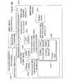
- FIG. 18Ais a simplified functional block diagram illustration of a NAND Flash device interacting with an external controller with Lee-metric based error correction encoding & decoding functionality in accordance with certain embodiments of the present invention
- FIG. 18Bis a simplified functional block diagram illustration of a flash memory system including an on-board microcontroller, with Lee-metric based error correction encoding & decoding functionality in accordance with certain embodiments of the present invention, wherein the encoding functionality may comprise any of the encoders of FIGS. 2 , 4 , 6 and 8 and the decoding functionality may comprise any of the decoders of FIGS. 3 , 5 , 7 and 9 respectively;
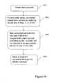
- FIG. 19is a simplified flowchart illustration of a method for effecting a NAND flash program command issued by the controller of FIG. 18A , in accordance with certain embodiments of the present invention.
- FIG. 20is a simplified flowchart illustration of a method for effecting a NAND flash read command issued by the controller of FIG. 18A , in accordance with certain embodiments of the present invention.
- Apparatus and methods for operating a flash deviceare now described, which are characterized by use of Lee distance based codes in the flash device so as to increase the number of errors that can be corrected for a given number of redundancy cells, compared with Hamming distance based codes.
- the Lee distance between two sequences of symbolsis the absolute sum of differences. If there are two symbols, S1 and S2, which take values between 0 and p ⁇ 1 where p is a prime number, then the Lee distance between these two symbols is then given by
- D ⁇ ( S 1 , S 2 )⁇ ⁇ S 1 - S 2 ⁇ ⁇ S 1 - S 2 ⁇ ⁇ ( p - 1 ) / 2 p - ⁇ S 1 - S 2 ⁇ ⁇ S 1 - S 2 ⁇ ⁇ ( p - 1 ) / 2 .
- ⁇ i0 n - 1 ⁇ D ⁇ ( S i , R i ) where n is the number of symbols in each of the two sequences.
- the measure between two sequencesis the number of level shifts assuming that per symbol there is a maximum of one error, i.e. either a single positive shift or a single negative shift; the Lee distance measure is suitable since the fact that multiple shifts per symbol are rare is now taken into account.
- gaincompared with binary BCH, results from the fact that less bits are now used to store a full symbol.
- flash memorynon-limiting and interchangeable (also referred to in general as “storage apparatus”).
- the elements associated with the storage apparatus as well as the sequence of operations carried outare integral to the storage apparatus.
- at least some of the elements associated with the storage apparatus and at least some of the related operationsare external to the flash, the solid state disk etc.
- some of the operations performed by microcontroller 110 of FIG. 18Amay be carried out by the central processing unit of the host 100 , without limiting the scope of the present invention.
- NAND Flash applicationssuch as SD cards and USB drives.
- the systemcomprises a controller 2400 and at least one NAND flash 2405 and perhaps many such as shown.
- the controller 2400interfaces to a host through a specified protocol. For example, in the case of a USB drive the protocol is that defined by universal serial bus protocol.
- the controller 2400then translates commands from the host. For example, read/write commands are translated into page read, page program and block erase commands on the Flash device 2405 through the NAND interface protocol.
- code operative in accordance with certain embodiments of this inventionmay be employed, e.g. by adding an encoding operation to each program command and adding a decoding operation to each read command.
- the encoding/decoding operations shown and described hereinmay replace existing encode/decode operations using less efficient codes.
- the NAND devices 2405are programmed page by page where each page may contain cells that store data and cells that store redundancy. Both sets of cells are used, such that the data and redundancy are spread over both.
- the page datais transferred as a sequence of bits and the bits are then mapped into cells.
- the output of encoder 2320is mapped into bits such that when stored in the Flash device, the bits are mapped back into symbols in Flash cells as defined by the encoders' output. This process is shown in FIG. 19 , for a programming procedure, and in FIG. 20 , for a read command.
- each physical pagei.e. page in the Flash array 2420
- each cellcontains a bit from each of the logical pages, mapped using Gray coding.
- the basic unitis two logical pages and each NAND flash read/program command is a sequence of two read/program commands of a logical page.
- a flash memory devicemay be provided whose internal or on-board microcontroller has Lee metric-based error correction encoder/decoder functionality capable of effectively correcting more errors than a binary BCH code for a given length of redundancy.
- encoding and decoding schemesin accordance with certain embodiments of the present invention, are now described, which employ four example codes respectively, termed the “syndrome separate” code, “syndrome separate, redundancy & data mixed” code, the “syndrome separate & shortened” code and the “syndrome separate & shortened, redundancy & data mixed” code respectively.
- Encoders and decoders employing these codes respectively, each constructed and operative in accordance with certain embodiments of the present inventionare presented in FIGS. 2 and 3 ; 4 and 5 ; 6 and 7 ; 8 and 9 respectively.
- the codesare used to encode information over a multi-level physical medium such as a Flash memory.
- the inputs and outputs of the Flash deviceare symbols containing L levels denoted by “0”, “1”, “2”, through “L ⁇ 1”.
- the inputs to the encoderare always assumed to be a sequence of bits while the inputs to the decoder are assumed to be a sequence of Flash symbols.
- the flash symbolscould be represented as a subset of a finite field. More precisely, these symbols may be viewed as a subset of a finite-filed GF(p) where p is a prime number.
- the encodersreceive k bits, where k is a predetermined constant, and produce n symbols, where n is a predetermined constant.
- nis such that n*log 2 L>k where n*log 2 L ⁇ k is, generally speaking, the number of spare bits allocated for the code for error correction purposes.
- the “syndrome separate” codeis characterized by a separately encoded syndrome.
- the “syndrome separate” codeis now described with reference to FIGS. 2 and 3 , and using the following symbols:
- Mapper A100 in FIG. 2
- wnumber of symbols produced by the Syndrome Computation block ( 110 ) of FIG. 2 .
- ⁇a non-zero element of GF(p) which is also a primitive element in GF(p).
- k′the number of bits mapped by the Demapper unit ( 120 ) following the mapping of the w symbols outputted by the Syndrome Computation block ( 110 ).
- n′number of bits at the output of the BCH encoder unit ( 130 ).
- r′number of symbols encapsulated at once by the Demapper unit ( 120 ).
- FIG. 2represents the “syndrome separate” encoder.
- the input to the encodera sequence of k bits, is mapped into t symbols by Mapper A ( 100 ).
- pis the smallest prime larger than or equal to t.
- Lis a power of 2
- the datais divided into subsequences of log 2 L bits, each subsequence being mapped into a symbol between 0 to L ⁇ 1, these symbols being numbers in the prime field GF(p).
- Mappingmay be effected e.g. by mapping each subsequence into a number represented by the binary representation of that sequence as shown in the table of FIG. 10A .
- Gray codingis not crucial for Mapper A because the performance of the code is not degraded if a different mapping is used, due to the fact that the encoding scheme shown and described herein works on entire symbols and not on individual bits.
- Lis not a power of 2 encapsulation may be used, typically dividing the input sequence into subsequences of r bits which are then translated into a sequence of
- Symbol counterremainder of the division of Z by L; and computation of Z as the quotient of the division of the previous Z by L.
- ris a predefined constant chosen to maximize the efficiency of encapsulation but yet sufficiently small to allow adequate implementation of the method in FIG. 11 either in hardware or software.
- the output of Mapper A ( 100 )then goes to a delay line block ( 150 ) and to a Syndrome computation block ( 110 ).
- the purpose of the delay line ( 150 )is to delay the sequence of the t symbols produced by the Mapper A block ( 100 ) such that the first symbols produced by ( 140 ) follow immediately after the last symbol was outputted from delay line ( 150 ).
- the Syndrome computation block ( 110 )produces w elements in GF(p). As described above, the t symbols outputted from Mapper A block ( 100 ) are treated like numbers in the field GF(p). The Syndrome computation block ( 110 ) then performs the following computation:
- the output of the Syndrome computation unit ( 110 )then flows to the Demapper unit ( 120 ).
- the Demappermaps the w GF(p) symbols into k′ bits, again, typically by using encapsulation. That is, the w symbols are divided into subsets each including r′ symbols, other than, possibly, one subset which has less than r′ symbols. Each subset is then mapped into bits using the binary representation of the number (now in the standard field):
- ⁇ i0 r ′ - 1 ⁇ S i ⁇ p i . This number is mapped into a sequence of ⁇ r′ ⁇ log 2 p ⁇ bits.
- the output of the Demapper ( 120 )flows into a binary BCH encoder ( 130 ) which receives k′ bits and produces n′ bits which include, on top of the original k′ bits, additional n′ ⁇ k′ redundancy bits which are used for error correction in the decoding process.
- the binary BCH encoderis a standard encoder as is known in the art such as any of these described in references [1], [2] and [3] and designed to function over GF(2 ⁇ log 2 n′ ⁇ ).
- the output of the binary BCH encoder ( 130 )is then mapped into symbol Mapper B ( 140 ) which receives n′ bits and maps them into n ⁇ t symbols.
- the mappingis performed similarly to that performed by Mapper A, typically using Gray coding. Again, if the number of levels is not a power of 2, encapsulation is effected as for Mapper A. If L is a power of 2 then the sequence of n′ bits is simply divided into subsets of log 2 L bits. If the sequence does not exactly divide, the sequence is zero padded until it is divided by log 2 L without a quotient. The subsets of log 2 L bits are then mapped using Gray coding as shown e.g. in the table of FIG. 10B .
- a Selector ( 160 )enables the flow of either the mapped original data from the delay line or the mapped redundancy data from Mapper B ( 140 ). At first, typically the selector enables the delay line to flow out; once this has occurred, the output of Mapper B ( 140 ) flows out.
- the delay lineis designed to delay the output of Mapper A ( 100 ) such that the output of Mapper B is synchronized to the end of the output of the delay line. The end result is a codeword as shown in FIG. 15 .
- the codeword of FIG. 15typically comprises a first portion ( 1500 ) which includes a mapping of the data sequence into L levels, and a second portion ( 1510 ) which is used as redundancy for the purpose of error correction of the information in the first portion 1500 .
- Second portion 1510is also mapped into L levels and also typically comprises two portions: a first portion ( 1520 ) including the mapping of the syndrome (computed from portion 1500 ) mapped into bits and then mapped to L levels; and a second portion ( 1530 ) including the mapping to L levels of the redundancy as computed by the BCH encoder of the portion ( 1520 ).
- FIG. 3shows a schematic view of the “syndrome separate” decoder.
- the “syndrome separate” decoder of FIG. 3typically receives n symbols from the Flash device and produces k correct bits.
- the n received symbolsbelong to one of L levels and may contain errors causing the wrong level to be read.
- the first t symbolsare associated with actual data whereas the last n ⁇ t symbols are associated with redundancy.
- the first t symbols and the last n ⁇ t symbolsmay be sent to the decoder of FIG. 3 simultaneously and analyzed simultaneously. If all n symbols are not sent simultaneously to the decoder, it is more efficient to send the last n ⁇ t symbols, which store the redundancy, first, followed by the first t symbols. The redundancy may then be decoded as the rest of the symbols are being sent to the decoder.
- the first t symbolsare sent to the Syndrome Computation unit which typically performs the same task as was performed by syndrome computation unit 110 in the “syndrome separate” encoder of FIG. 2 .
- the last n ⁇ t symbolsare sent to a Demapper B 200 which performs the converse of the operation performed by the Mapper B ( 140 ) in FIG. 2 .
- the Demapperreceives n ⁇ t symbols and produces n′ bits.
- the Demapper 200simply produces log 2 L bits for every symbol, the bits being produced by a process of Gray coding e.g. according to the table of FIG. 10B . If L is not a power of 2, de-encapsulation is performed to reverse the effect of encapsulation. That is, the n ⁇ t symbols are divided into sub-sequences of ⁇ r/log 2 L ⁇ symbols from which the Demapper B 200 produces r bits.
- the binary output of the Demapper 200is a sequence of n′ bits which are passed to the binary BCH decoder ( 210 ) which corrects any errors which might have occurred in the redundancy symbols.
- the BCH decodingmay be effected as known in the art e.g. as described in references ([1], [2], [3]).
- the BCH decoder ( 210 )outputs k′ bits which were used to code the Syndrome during the encoding process performed by the encoder of FIG. 2 .
- the k′ bitsare passed to a mapper unit ( 220 ) which produces w symbols over GF(p). This time the symbols may assume values from 0 to p ⁇ 1.
- the mapper unit ( 220 )performs the converse of the operation performed by the Demapper unit ( 120 ) in the encoder of FIG. 2 , e.g. by De-encapsulation.
- the k′ bitsare divided into subsets of ⁇ r′ ⁇ log 2 p ⁇ .
- the symbolsmay be derived by representing the subset as a number (in the normal field) and performing the method in FIG. 13 .
- Zinitially, is the number represented by the ⁇ r′ ⁇ log 2 p ⁇ bits and the following computations are repeated r′ times:
- the output of Mapper ( 220 )is the accurate Syndrome whereas the output of the Syndrome Computation unit ( 230 ) is the estimated syndrome according to the received symbols from the device. The difference between them is the syndrome only due to the error.
- the output of the subtract block ( 240 )is the difference (symbol by symbol) of the two syndromes and is the syndrome of the errors that occurred in the first t symbols.
- the eligible word which is closest (by the Lee metric) to the word actually receivedis recovered by best eligible word recovery block 250 . Any suitable conventional method can be used to effect the recovery, such as that described in steps 2-5 on page 311 Section 10.4 (“Decoding alternant codes in the Lee metric”), in reference [2].
- Demapper Amaps the t symbols back into k bits.
- the Demapper Aundoes the operation of Mapper A ( 100 ) in the “syndrome separate” encoder of FIG. 2 , similarly to Demapper B. However, it is not necessary to use Gray mapping.
- the length of the input sequence (in bits) and the length of the code word (in symbols)are given by conventional design preferences that are typically unaffected by the teachings of the invention shown and described herein, so k and n are assumed to be known. Therefore, values for the constant p and the number of symbols that contain data t are also immediately available.
- the encapsulation parameters r and r′are determined by hardware complexity restrictions; for example, r may not be limited to less than 128 bits.
- the remaining parametersmay be determined by trading off the number of BCH redundancy bits n′ ⁇ k′ and the number of Syndrome symbols w, it being appreciated that n′ bits may be stored in n ⁇ t symbols. The tradeoff is typically between the number of bits (n′ ⁇ k′) allocated to correct the “accurate” Syndrome and the number of symbols (w): allocated to correct the data referred to above, as stored in the word referred to above.
- P errdenotes the frame error rate and P cross denotes the probability that an individual level is erroneously read as either the following or preceding level.
- the probability of errormay be approximated by assuming that errors only occur between nearby levels.
- a decoding errormay occur if either one of the following events occurs:
- “syndrome separate, redundancy & data mixed” codethe redundancy symbols are no longer separated from the data symbols but rather mixed with them. This is done in such a manner that the error probability in the redundancy information is decreased.
- pthe prime used for the Lee-metric code
- nwhich may decrease the error correction capability of the Lee-metric decoder.
- the number of levels, Lis assumed above to be a power of 2. However, where L is not a power of 2, encapsulation may be used, as described generally above.
- the following symbolsare used in the description of the “syndrome separate, redundancy & data mixed” code:
- D i (i0 . . . n ⁇ 1)—Combined symbol output of Mapper A ( 300 ) and A′ ( 310 ) comprising numbers in GF(p) with values between 0 and L ⁇ 1.
- k′the number of bits mapped by the Demapper unit ( 350 ) following the mapping of the w symbols outputted by the Syndrome Computation block ( 340 ).
- n′number of bits at the output of the BCH encoder unit ( 360 ).
- the w symbolsthen flow into the Demapper ( 350 ) which performs the same task as performed by the Demapper unit ( 120 ) in the “syndrome separate” encoder.
- the output of the Demapper ( 350 )is k′ bits which flow into the binary BCH encoder ( 360 ) which produces n′ bits.
- unit 360is identical to unit 130 in the “syndrome separate” encoder of FIG. 2 .
- Mapper BThe purpose of Mapper B is to combine the outputs of the Mapper A′ ( 310 ) with the output of the BCH encoder. More precisely, Mapper A′ ( 310 ) produces ⁇ (k ⁇ t ⁇ log 2 L)/(log 2 L ⁇ 1) ⁇ symbols with values between 0 and L/2 ⁇ 1.
- Y iare the symbols at the output of the Mapper B ( 370 ) unit
- D iare the symbols at the output of the Selector unit ( 320 )
- b iare the bits (with values of 0 and 1) at the output of the BCH encoder ( 360 ).
- the end result of this processis a codeword structured as shown in FIG. 16 which comprises 2 portions.
- the first portion ( 2100 )includes the mapping of t ⁇ log 2 L data bits into L-level symbols.
- the second portion ( 2110 )includes both data and redundancy mapped into L-level symbols. This is done by letting the data determine the log 2 L ⁇ 1 LSB bits of the index of the L-level symbol.
- the syndrome (after mapping it into bits) and the redundancy of the BCH codesdetermine the most significant bit of the index of the L-level symbol.
- FIG. 5gives a schematic view of a decoder for the “syndrome separate, redundancy & data mixed” code.
- the n symbols of the codeflow simultaneously into Demapper A′ ( 400 ) and Demapper A ( 430 ).
- Demapper A ( 430 )handles separately the first t symbols and the latter n′ symbols.
- the first t symbolsare passed ‘as is’ to the Syndrome computation unit ( 440 ) while the latter n′ symbols are stripped from the Redundancy information produced by the BCH encoder ( 360 ) in the encoder. This is done as follows:
- ⁇ circumflex over (F) ⁇ circumflex over (F 1 ) ⁇is the output of Demapper A and F i is the input.
- Demapper A′( 400 ) is a sequence of n′ bits which are decoded by the binary BCH decoder ( 410 ) which produces k′ bits. These bits are then mapped back into w symbols over GF(p) by the Mapper ( 420 ) which performs the same task as the Mapper ( 220 ) in the “syndrome separate” decoder of FIG. 3 .
- the output of Demapper A ( 430 )flows into the Syndrome computation unit ( 440 ) which performs the same task as the Syndrome computation unit ( 340 ) in the encoder.
- the output of Mapper ( 420 )are the “accurate” syndrome symbols while the output of the syndrome computation unit ( 440 ) is a result of errors symbols.
- the difference between these syndromesis the syndrome due to the errors alone. This difference is computed by the Subtract unit ( 450 ).
- Unit 460receives the output of 450 and Demapper A, and recovers the accurate symbols. Any suitable conventional method can be used to effect the recovery, such as that described in steps 2-5 on page 311 Section 10.4 (“Decoding alternant codes in the Lee metric”), in reference [2].
- the output of 460flows into the Demapper B ( 470 ) which performs the reverse operation of Mapper A ( 300 ) for symbols 0 . . . t ⁇ 1 and Mapper A′ ( 310 ) for symbols t . . . n ⁇ 1.
- the outputis the reconstructed input stream.
- the “syndrome separate & shortened” codecharacterized by a separately encoded shortened Syndrome, is now described.
- the “syndrome separate & shortened” code embodimentimproves the “syndrome separate” code embodiment at the expense of adding w 2 multiplications over GF(p).
- the following symbolsare used to describe the “syndrome separate & shortened” code:
- Mapper A500
- ⁇a non-zero element of GF(p) (i.e. a number between 1 and p ⁇ 1).
- k′the number of bits mapped by the Demapper unit ( 540 ) following the mapping of the w symbols outputted from the Roundup unit ( 530 ).
- n′number of bits at the output of the BCH encoder unit ( 550 ).
- r′number of symbols encapsulated in unison (in parallel) by the Demapper unit ( 540 ).
- FIG. 6illustrates an encoder of the “syndrome separate & shortened” code which is similar to the “syndrome separate” encoder of FIG. 2 but includes 2 additional units: xG ⁇ 1 unit 520 and roundup unit 530 .
- the operations of all other blockssubstantially resemble the operations of their counterparts in FIG. 2 , respectively.
- data in the form of a bit sequenceflows into Mapper A ( 500 ) and then to the syndrome computation unit ( 510 ). Both units, 500 and 510 , operate substantially as do their counterparts in the “syndrome separate” code encoder of FIG.
- G - 1( ⁇ t ⁇ 0 ⁇ ( t + 1 ) ⁇ 0 ⁇ ( t + 2 ) ⁇ 0 ... ⁇ ( t + w - 1 ) ⁇ 0 ⁇ t ⁇ 1 ⁇ ( t + 1 ) ⁇ 1 ⁇ ( t + 2 ) ⁇ 1 ⁇ t ⁇ 2 ⁇ ( t + 1 ) ⁇ 2 ⁇ ( t + 2 ) ⁇ 2 ⁇ ⁇ ⁇ ⁇ t + 2 ) ⁇ 2 ⁇ ⁇ ⁇ ⁇ t - 1 ) ⁇ ( w - 1 ) - 1 , where ⁇ is the primitive element in GF(p) used in the computation of the syndrome.
- the multiplication operationis defined as follows:
- the symbols T iwhich take only values between 0 and L ⁇ 1, are outputted to the Selector unit ( 580 ) which appends these symbols to the end of the t symbols holding the data.
- the symbols V iflow to the Demapper unit ( 540 ).
- V itypically only have ⁇ p/L ⁇ possible values, all divisible by L.
- the Demapper unit ( 540 )operates similarly to the Demapper ( 120 ) of the “syndrome separate” code encoder of FIG. 2 , however before performing the encapsulation, the symbols are divided by L and in the encapsulation process, the parameter p is exchanged with ⁇ p/L ⁇ . This yields a more compact presentation of the syndrome and diminishes the BCH code's requirements, thus allowing a tradeoff between w and n′ ⁇ k′ in the computation of the frame error rate to weigh in favor of w.
- the operations of the other units in FIG. 6are similar to those of their counterparts in the “syndrome separate” encoder of FIG. 2 .
- the end resultis a codeword as shown in FIG. 17 .
- the codeword of FIG. 17may include three portions.
- the first portion ( 2200 )is simply a mapping of the data sequence into L levels.
- the second portion ( 2210 )includes W L-level symbols which define a portion of the syndrome characterized in that the overall syndrome of the data symbols along with these W symbols has a significantly smaller set of possibilities.
- the third portion ( 2220 )includes some of the encoded syndrome (only the portion thereof which was to be defined) and is used as redundancy for purpose of error correction of the information in the first two portions 2200 and 2210 .
- the third portion 2220is also mapped into L levels and comprises:
- FIG. 7illustrates a “syndrome separate & shortened” decoder which is similar to the “syndrome separate” decoder of FIG. 3 , however, a matrix multiplier unit xG ( 640 ) is provided which multiplies the W-symbol output of the Mapper unit ( 630 ) by the following matrix G:
- G( ⁇ t ⁇ 0 ⁇ ( t + 1 ) ⁇ 0 ⁇ ( t + 2 ) ⁇ 0 ... ⁇ ( t + w - 1 ) ⁇ 0 ⁇ t ⁇ 1 ⁇ ( t + 1 ) ⁇ 1 ⁇ ( t + 2 ) ⁇ 1 ⁇ t ⁇ 2 ⁇ ( t + 1 ) ⁇ 2 ⁇ ( t + 2 ) ⁇ 2 ⁇ ⁇ ⁇ ⁇ t + 2 ) ⁇ 2 ⁇ ⁇ ⁇ ⁇ t - 1 ) ⁇ ( w - 1 ) ) .
- the Mapper unit ( 630 )is similar to Mapper unit ( 220 ) in the “syndrome separate” decoder of FIG. 2 , however, the parameter p is replaced with ⁇ p/L ⁇ and the outputs are multiplied by L. Also, the syndrome computation unit ( 610 ) operates over t+w elements whereas its counterpart in the “syndrome separate” decoder of FIG. 2 operates over t elements. The remaining units in the “syndrome separate & shortened” decoder of FIG. 7 can be generally identical to their counterparts in the “syndrome separate” code decoder of FIG. 2 .
- the probability of either of these eventsmay be bounded from above by
- a valuemay be selected which reduces the above probability, typically to a minimum.
- Mapper A ( 700 ) and A′ ( 710 )Comprising numbers in GF(p) with values between 0 and L ⁇ 1.
- k′the number of bits mapped by the Demapper unit ( 780 ) following the mapping of the w symbols outputted by the Syndrome Computation block ( 740 ).
- n′number of bits at the output of the BCH encoder unit ( 790 ).
- FIG. 8illustrates a “syndrome separate & shortened, redundancy & data mixed” encoder.
- the composition of the codewordis shown in FIG. 14 .
- the mid-section 1410comprises both data bits and encoded syndrome bits (what is left of it following the use of the additional w symbols appended to the end of the codeword) as shown in FIG. 16 in portions 2120 and 2130 .
- a matrix multiplier xG ⁇ 1 ( 750 ) and a roundup unit ( 760 )which may be generally similar to their counterparts in the “syndrome separate & shortened” encoder of FIG. 6 namely units 520 and 530 respectively.
- the matrix multiplier xG ⁇ 1 ( 750 )typically computes the following:
- the Demapper unit ( 780 )may be similar to Demapper ( 350 ) of the “syndrome separate, redundancy & data mixed” encoder of FIG. 4 , however typically, before demapper 780 performs encapsulation, the symbols are divided by L and in the encapsulation process, the parameter p is exchanged with ⁇ p/L ⁇ , all in contrast to demapper 350 , to provide a more compact presentation of the syndrome and diminish the requirements from the BCH, thereby allowing the tradeoff between w and n′ ⁇ k′ in the computation of the frame error rate to weigh in favor of w.
- the operation of the other unitsmay be similar to that of their counterparts in the “syndrome separate, redundancy & data mixed” encoder of FIG.
- FIG. 9illustrates a “syndrome separate & shortened, redundancy & data mixed” decoder which is similar to the “syndrome separate, redundancy & data mixed” decoder of FIG. 5 , however, in FIG. 9 , a matrix multiplier unit xG ( 930 ) is provided which receives the output of w symbols of the Mapper unit ( 920 ) and multiplies it by the following matrix G:
- the Mapper unit ( 920 )may be generally similar to the Mapper unit ( 420 ) in the “syndrome separate” decoder of FIG.
- the parameter pis replaced with ⁇ p/L ⁇ and the outputs are multiplied by L.
- the remaining units of FIG. 9may be generally similar to their “syndrome separate, redundancy & data mixed” code counterparts in the embodiment of FIG. 5 .
- a decoding errormay occur if either one of the following events occurs:
- Lee distance based codesrather than Hamming distance based codes is a particular advantage in flash memory devices constructed and operative in accordance with certain embodiments of the present invention because if gray mapping is being used in a flash memory device, errors almost always involve a symbol being confounded with a neighboring symbol in the mapping scheme rather than with a distant symbol in the mapping scheme, such that use of Lee distance based code may give better error correction functionality per unit of redundancy or less redundancy for a given level of error correction functionality adequacy.
- software components of the present inventionincluding programs and data may, if desired, be implemented in ROM (read only memory) form including CD-ROMs, EPROMs and EEPROMs, or may be stored in any other suitable computer-readable medium such as but not limited to disks of various kinds, cards of various kinds and RAMs.
- ROMread only memory
- EEPROMelectrically erasable programmable read-only memory
- Components described herein as softwaremay, alternatively, be implemented wholly or partly in hardware, if desired, using conventional techniques.
- Any data described as being stored at a specific location in memorymay alternatively be stored elsewhere, in conjunction with an indication of the location in memory with which the data is associated.
- the samemay be stored within the flash memory device's internal microcontroller or within a microcontroller interfacing between the flash memory device and the host, and an indication may be stored of the specific page or erase sector associated with the cells.
- the flash controlling apparatuscontrols a flash memory array and may comprise either a controller external to the flash array or a microcontroller on-board the flash array or otherwise incorporated therewithin.
- flash memory arraysinclude Samsung's K9XXG08UXM series, Hynix' HY27UK08BGFM Series, Micron's MT29F64G08TAAWP or other arrays such as but not limited to NOR or phase change memory.
- controllerswhich are external to the flash array they control include STMicroelectrocincs's ST7265x microcontroller family, STMicroelectrocincs's ST72681 microcontroller, and SMSC's USB97C242, Traspan Technologies' TS-4811, Chipsbank CBM2090/CBM1190.
- Example of commercial IP software for Flash file systemsare: Denali's SpectraTM NAND Flash File System, Aarsan's NAND Flash Controller IP Core and Arasan's NAND Flash File System. It is appreciated that the flash controller apparatus need not be NAND-type and can alternatively, for example, be NOR-type or phase change memory-type.
- Flash controlling apparatuswhether external or internal to the controlled flash array, typically includes the following components: a Memory Management/File system, a NAND interface (or other flash memory array interface), a Host Interface (USB, SD or other), error correction circuitry (ECC) typically comprising an Encoder and matching decoder, and a control system managing all of the above.
- a Memory Management/File systemtypically includes the following components: a Memory Management/File system, a NAND interface (or other flash memory array interface), a Host Interface (USB, SD or other), error correction circuitry (ECC) typically comprising an Encoder and matching decoder, and a control system managing all of the above.
- the present inventionmay for example interface with or modify, as per any of the embodiments described herein, one, some or all of the above components and particularly with the ECC component.
Landscapes
- Health & Medical Sciences (AREA)
- Engineering & Computer Science (AREA)
- Natural Medicines & Medicinal Plants (AREA)
- Theoretical Computer Science (AREA)
- Physics & Mathematics (AREA)
- Life Sciences & Earth Sciences (AREA)
- General Physics & Mathematics (AREA)
- General Engineering & Computer Science (AREA)
- Quality & Reliability (AREA)
- Probability & Statistics with Applications (AREA)
- Biotechnology (AREA)
- Veterinary Medicine (AREA)
- Pharmacology & Pharmacy (AREA)
- Epidemiology (AREA)
- Animal Behavior & Ethology (AREA)
- General Health & Medical Sciences (AREA)
- Public Health (AREA)
- Mycology (AREA)
- Microbiology (AREA)
- Medicinal Chemistry (AREA)
- Medical Informatics (AREA)
- Botany (AREA)
- Alternative & Traditional Medicine (AREA)
- Chemical & Material Sciences (AREA)
- Techniques For Improving Reliability Of Storages (AREA)
- Detection And Correction Of Errors (AREA)
Abstract
Description
- Paulo Cappelletti, Clara Golla, Piero Olivo, Enrico Zanoni, “Flash Memories”, Kluwer Academic Publishers, 1999
- G. Campardo, R. Micheloni, D. Novosel, “CLSI-Design of Non-Volatile Memories”, Springer Berlin Heidelberg New York, 2005
- [1] “Error Correction Coding Mathematical Methods and Algorithms”, Todd K. Moon, A JOHN WILEY & SONS, INC., 2005.
- [2] “Introduction to Coding Theory”, Ron M. Roth, Cambridge University Press, 2006.
- [3] “Algebraic Codes for Data Transmission”, Richard E. Blahut, Cambridge University Press, 2003.
Block: a set of flash memory device cells which must, due to physical limitations of the flash memory device, be erased together. Also termed erase sector, erase block.
Cell: A component of flash memory that stores one bit of information (in single-level cell devices) or n bits of information (in a multi-level device having 2 exp n levels). Typically, each cell comprises a floating-gate transistor. n may or may not be an integer. “Multi-level” means that the physical levels in the cell are, to an acceptable level of certainty, statistically partionable into multiple distinguishable regions, plus a region corresponding to zero, such that digital values each comprising multiple bits can be represented by the cell. In contrast, in single-level cells, the physical levels in the cell are assumed to be statistically partitionable into only two regions, one corresponding to zero and one other, non-zero region, such that only one bit can be represented by a single-level cell.
Charge level: the measured voltage of a cell which reflects its electric charge.
Cycling: Repeatedly writing new data into flash memory cells and repeatedly erasing the cells between each two writing operations.
Decision regions: Regions extending between adjacent decision levels, e.g. if decision levels are 0, 2 and 4 volts respectively, the decision regions are under 0 V, 0 V-2 V, 2V-4 V, and over 4 V.
Demapping: basic cell-level reading function in which a digital n-tuple originally received from an outside application is derived from a physical value representing a physical state in the cell having a predetermined correspondence to the digital n-tuple.
Digital value or “logical value”: n-tuple of bits represented by a cell in flash memory an capable of generating 2 exp n distinguishable levels of a typically continuous physical value such as charge, where n may or may not be an integer.
Erase cycle: The relatively slow process of erasing a block of cells (erase sector), each block typically comprising more than one page, or, in certain non-flash memory devices, of erasing a single cell or the duration of so doing. An advantage of erasing cells collectively in blocks as in flash memory, rather than individually, is enhanced programming speed: Many cells and typically even many pages of cells are erased in a single erase cycle.
Erase-write cycle: The process of erasing a block of cells (erase sector), each block typically comprising a plurality of pages, and subsequently writing new data into at least some of them. The terms “program” and “write” are used herein generally interchangeably.
Flash memory: Non-volatile computer memory including cells that are erased block by block, each block typically comprising more than one page, but are written into and read from, page by page. Includes NOR-type flash memory, NAND-type flash memory, and PRAM, e.g. Samsung PRAM, inter glia, and flash memory devices with any suitable number of levels per cell, such as but not limited to 2, 4, or 8.
Mapping: basic cell-level writing function in which incoming digital n-tuple is mapped to a program level by inducing a program level in the cell, having a predetermined correspondence to the incoming logical value.
Page: A portion, typically 512 or 2048 or 4096 bytes in size, of a flash memory e.g. a NAND or NOR flash memory device. Writing can be performed page by page, as opposed to erasing which can be performed only erase sector by erase sector. A few bytes, typically 16-32 for every 512 data bytes are associated with each page (typically 16, 64 or 128 per page), for storage of error correction information. A typical block may include 32 512-byte pages or 64 2048-byte pages.
Precise read, soft read: Cell threshold voltages are read at a precision (number of bits) greater than the number of Mapping levels (2^n). The terms precise read or soft read are interchangeable. In contrast, in “hard read”, cell threshold voltages are read at a precision (number of bits) smaller than the number of Mapping levels (2^n where n=number of bits per cell).
Present level, Charge level: The amount of charge in the cell. The Amount of charge currently existing in a cell, at the present time, as opposed to “program level”, the amount of charge originally induced in the cell (i.e. at the end of programming)
Program: same as “write”.
Program level (programmed level, programming level): amount of charge originally induced in a cell to represent a given logical value, as opposed to “present level”.
Reprogrammability (Np): An aspect of flash memory quality. This is typically operationalized by a reprogrammability parameter, also termed herein “Np”, denoting the number of times that a flash memory can be re-programmed (number of erase-write cycles that the device can withstand) before the level of errors is so high as to make an unacceptably high proportion of those errors irrecoverable given a predetermined amount of memory devoted to redundancy. Typically recoverability is investigated following a conventional aging simulation process which simulates or approximates the data degradation effect that a predetermined time period e.g. a 10 year period has on the flash memory device, in an attempt to accommodate for a period of up to 10 years between writing of data in flash memory and reading of the data therefrom.
Resolution: Number of levels in each cell, which in turn determines the number of bits the cell can store; typically a cell with 2^n levels stores n bits. Low resolution (partitioning the window, W, of physical values a cell can assume into a small rather than large number of levels per cell) provides high reliability.
Retention: of original physical levels induced in the cells; retention is typically below 100% resulting in deterioration of original physical levels into present levels.
Retention time: The amount of time that data has been stored in a flash device, typically without, or substantially without, voltage having been supplied to the flash device i.e. the time which elapses between programming of a page and reading of the same page.
Symbol: Logical value
Threshold level: the voltage (e.g.) against which the charge level of a cell is measured. For example, a cell may be said to store a particular digital n-tuple D if the charge level or other physical level of the cell falls between two threshold values T.
where n is the number of symbols in each of the two sequences.
symbols over GF(p) where each symbol is one of 0, 1, . . . , L−1. This may be done by representing the r bits as a number (in the standard number field) and following the procedure described in
times: Symbolcounter=remainder of the division of Z by L; and computation of Z as the quotient of the division of the previous Z by L. r is a predefined constant chosen to maximize the efficiency of encapsulation but yet sufficiently small to allow adequate implementation of the method in
where Di(i=0 . . . t−1) are the output symbols of Mapper A (100), Sj(j=0 . . . w−1) are the output symbols of the Syndrome computation block (110) and a is a number between 1 and p−1 which is also a primitive element in GF(p). All multiplications and additions are carried out in the GF(p) field (i.e. modulo p). Finite fields, primitive elements, and other related aspects of the above computations are described in documents [2] and [3].
This number is mapped into a sequence of ┌r′·log2p┐ bits.
times and the output is the binary representation of the final value of Z.
- 1. An error occurs in the decoding of “accurate” Syndrome (210). i.e., there were more than └(n′−k′)/┌ log2n′┐┘ errors in the (n-t) symbols allocated to store the redundancy.
- 2. An error occurs in the decoding of the data symbols using the Lee metric decoder (240). i.e., there were w or more errors in the first t symbols.
- The probability of any of these events may be bounded from above by
- Thus, by enumerating over w, a value may be selected which reduces the above probability, typically to a minimum.
FIG. 4 shows a schematic view of an encoder for the “syndrome separate, redundancy & data mixed” code. The input is a sequence of bits (k bits) which flows into Mappers A (300) and A′ (310). The first t·log2L bits are mapped by Mapper A into symbols over GF(p) with values between 0 and L−1. Mapper divides the t·log2L bits into subsequences of log2L which are mapped into symbols using any type of mapping (for example the mappings in the tables inFIG. 10 ). It is appreciated that the choice of the mapping does not affect the performance of the code. The last k−t·log2L bits of the input sequence are mapped by Mapper A′ into symbols over GF(p) with values between 0 and L/2-1. This is done by dividing the remaining bits into subsequences of log2L−1 bits and mapping the subsequences into symbols according to any mapping scheme.- The Selector (320) simply adjust the flow of the symbols such that the symbols generated by Mapper A′ (310) follow the last symbols generated by Mapper A (300). Overall, there are n symbols (i.e. n=t+┌(k−t·log2L)/(log2L−1)┐).
The symbols flow into the syndrome computation unit (340) which performs the same task as performed by the syndrome computation unit (110) in the “syndrome separate” encoder ofFIG. 2 . This unit produces w symbols over GF(p) (this time, the symbols take any value between 0 and p−1).
Yi=Di+bi·L/2, i=n−n′ . . . n−1,
where {circumflex over (F)}{circumflex over (F1)} is the output of Demapper A and Fiis the input. Demapper A′ (400) only handles the last n′ symbols and recovers from them only the redundancy bits produced by the BCH encoder by computing bi=└Yi/(L/2)┘ for i=t . . . n−1.
The output of Demapper A′ (400) is a sequence of n′ bits which are decoded by the binary BCH decoder (410) which produces k′ bits. These bits are then mapped back into w symbols over GF(p) by the Mapper (420) which performs the same task as the Mapper (220) in the “syndrome separate” decoder of
- 1. An error occurs in the decoding of “accurate” Syndrome (410). i.e., there were more than └n′−k′)/┌ log2n′┐┘ errors in the (n−t) symbols allocated to store the redundancy. The probability of bit error is Pcross/(L/2).
- 2. An error occurs in the decoding of the data symbols using the Lee metric decoder (460) indicating that there were w or more errors in one of the n symbols.
- The probability of any of these events may be upper-bounded by
- Thus, by enumerating over w, a value may be selected which brings the above probability to a minimum.
- The improvement in the above expression here compared with that obtained for the “syndrome separate” code is in the first summand which now includes a small probability: Pcross(L/2). This probability may be compared with the probability appearing for the “syndrome separate” code after normalizing with the number of bits per symbol; the comparison being
where α is the primitive element in GF(p) used in the computation of the syndrome. The multiplication operation is defined as follows:
where Ziare the outputs of the matrix multiplication unit.
The Mapper unit (630) is similar to Mapper unit (220) in the “syndrome separate” decoder of
- 1. An error occurs in the decoding of “accurate” Syndrome (610), e.g. there are more than └(n′−k′)/┌ log2n′┐┘ errors in the (n−t−w) symbols allocated to store the redundancy.
- 2. An error occurs in the decoding of the data symbols using the Lee metric decoder (660), e.g. there are w or more errors in the first t+w symbols.
where Ziare the outputs of the matrix multiplication unit.
- 1. An error occurs in the decoding of “accurate” Syndrome (910), e.g. there are more than └(n′−k′)/┌ log2n′┐┘ errors in the (n′=n−t−w) symbols allocated to store the redundancy. Now, the probability of bit error is given by Pcross/(L/2).
- 2. An error occurs in the decoding of the data symbols using the Lee metric decoder (970), e.g. there were w or more errors in n symbols.
- The probability of any of these events may be bounded from above by
- Thus, by enumerating over w, a value may be selected which reduces the above probability, e.g. to a minimum.
- It will also be understood that the system according to the invention may be a suitably programmed computer. Likewise, the invention contemplates a computer program being readable by a computer for executing the method of the invention. The invention further contemplates a machine-readable memory tangibly embodying a program of instructions executable by the machine for executing the method of the invention.
Claims (23)
Priority Applications (2)
| Application Number | Priority Date | Filing Date | Title |
|---|---|---|---|
| US13/746,072US8782500B2 (en) | 2007-12-12 | 2013-01-21 | Systems and methods for error correction and decoding on multi-level physical media |
| US14/307,213US20140365847A1 (en) | 2007-12-12 | 2014-06-17 | Systems and methods for error correction and decoding on multi-level physical media |
Applications Claiming Priority (8)
| Application Number | Priority Date | Filing Date | Title |
|---|---|---|---|
| US99694807P | 2007-12-12 | 2007-12-12 | |
| US638508P | 2008-01-10 | 2008-01-10 | |
| US6499508P | 2008-04-08 | 2008-04-08 | |
| US7146808P | 2008-04-30 | 2008-04-30 | |
| US7148708P | 2008-05-01 | 2008-05-01 | |
| PCT/IL2008/001229WO2009074978A2 (en) | 2007-12-12 | 2008-09-17 | Systems and methods for error correction and decoding on multi-level physical media |
| US12/667,043US8359516B2 (en) | 2007-12-12 | 2008-09-17 | Systems and methods for error correction and decoding on multi-level physical media |
| US13/746,072US8782500B2 (en) | 2007-12-12 | 2013-01-21 | Systems and methods for error correction and decoding on multi-level physical media |
Related Parent Applications (3)
| Application Number | Title | Priority Date | Filing Date |
|---|---|---|---|
| PCT/IL2008/001229ContinuationWO2009074978A2 (en) | 2007-12-12 | 2008-09-17 | Systems and methods for error correction and decoding on multi-level physical media |
| US12/667,043ContinuationUS8359516B2 (en) | 2007-12-12 | 2008-09-17 | Systems and methods for error correction and decoding on multi-level physical media |
| US66704309AContinuation | 2007-12-12 | 2009-12-29 |
Related Child Applications (1)
| Application Number | Title | Priority Date | Filing Date |
|---|---|---|---|
| US14/307,213ContinuationUS20140365847A1 (en) | 2007-12-12 | 2014-06-17 | Systems and methods for error correction and decoding on multi-level physical media |
Publications (2)
| Publication Number | Publication Date |
|---|---|
| US20130139037A1 US20130139037A1 (en) | 2013-05-30 |
| US8782500B2true US8782500B2 (en) | 2014-07-15 |
Family
ID=40755951
Family Applications (3)
| Application Number | Title | Priority Date | Filing Date |
|---|---|---|---|
| US12/667,043Active2029-08-22US8359516B2 (en) | 2007-12-12 | 2008-09-17 | Systems and methods for error correction and decoding on multi-level physical media |
| US13/746,072ActiveUS8782500B2 (en) | 2007-12-12 | 2013-01-21 | Systems and methods for error correction and decoding on multi-level physical media |
| US14/307,213AbandonedUS20140365847A1 (en) | 2007-12-12 | 2014-06-17 | Systems and methods for error correction and decoding on multi-level physical media |
Family Applications Before (1)
| Application Number | Title | Priority Date | Filing Date |
|---|---|---|---|
| US12/667,043Active2029-08-22US8359516B2 (en) | 2007-12-12 | 2008-09-17 | Systems and methods for error correction and decoding on multi-level physical media |
Family Applications After (1)
| Application Number | Title | Priority Date | Filing Date |
|---|---|---|---|
| US14/307,213AbandonedUS20140365847A1 (en) | 2007-12-12 | 2014-06-17 | Systems and methods for error correction and decoding on multi-level physical media |
Country Status (2)
| Country | Link |
|---|---|
| US (3) | US8359516B2 (en) |
| WO (1) | WO2009074978A2 (en) |
Cited By (2)
| Publication number | Priority date | Publication date | Assignee | Title |
|---|---|---|---|---|
| US20140223228A1 (en)* | 2011-05-02 | 2014-08-07 | Samsung Electronics Co., Ltd. | Memory system and error correction method |
| US20140237313A1 (en)* | 2013-02-19 | 2014-08-21 | Lsi Corporation | Systems and Methods for Trapping Set Disruption |
Families Citing this family (147)
| Publication number | Priority date | Publication date | Assignee | Title |
|---|---|---|---|---|
| WO2007132456A2 (en) | 2006-05-12 | 2007-11-22 | Anobit Technologies Ltd. | Memory device with adaptive capacity |
| KR101202537B1 (en) | 2006-05-12 | 2012-11-19 | 애플 인크. | Combined distortion estimation and error correction coding for memory devices |
| WO2007132453A2 (en) | 2006-05-12 | 2007-11-22 | Anobit Technologies Ltd. | Distortion estimation and cancellation in memory devices |
| WO2008026203A2 (en) | 2006-08-27 | 2008-03-06 | Anobit Technologies | Estimation of non-linear distortion in memory devices |
| US7975192B2 (en) | 2006-10-30 | 2011-07-05 | Anobit Technologies Ltd. | Reading memory cells using multiple thresholds |
| WO2008053473A2 (en) | 2006-10-30 | 2008-05-08 | Anobit Technologies Ltd. | Memory cell readout using successive approximation |
| US7924648B2 (en) | 2006-11-28 | 2011-04-12 | Anobit Technologies Ltd. | Memory power and performance management |
| WO2008068747A2 (en) | 2006-12-03 | 2008-06-12 | Anobit Technologies Ltd. | Automatic defect management in memory devices |
| US7900102B2 (en) | 2006-12-17 | 2011-03-01 | Anobit Technologies Ltd. | High-speed programming of memory devices |
| US8151166B2 (en) | 2007-01-24 | 2012-04-03 | Anobit Technologies Ltd. | Reduction of back pattern dependency effects in memory devices |
| US7751240B2 (en) | 2007-01-24 | 2010-07-06 | Anobit Technologies Ltd. | Memory device with negative thresholds |
| US8369141B2 (en) | 2007-03-12 | 2013-02-05 | Apple Inc. | Adaptive estimation of memory cell read thresholds |
| US8001320B2 (en) | 2007-04-22 | 2011-08-16 | Anobit Technologies Ltd. | Command interface for memory devices |
| WO2008139441A2 (en) | 2007-05-12 | 2008-11-20 | Anobit Technologies Ltd. | Memory device with internal signal processing unit |
| US8234545B2 (en) | 2007-05-12 | 2012-07-31 | Apple Inc. | Data storage with incremental redundancy |
| US7925936B1 (en) | 2007-07-13 | 2011-04-12 | Anobit Technologies Ltd. | Memory device with non-uniform programming levels |
| US8259497B2 (en) | 2007-08-06 | 2012-09-04 | Apple Inc. | Programming schemes for multi-level analog memory cells |
| US8174905B2 (en) | 2007-09-19 | 2012-05-08 | Anobit Technologies Ltd. | Programming orders for reducing distortion in arrays of multi-level analog memory cells |
| US8650352B2 (en) | 2007-09-20 | 2014-02-11 | Densbits Technologies Ltd. | Systems and methods for determining logical values of coupled flash memory cells |
| US8365040B2 (en) | 2007-09-20 | 2013-01-29 | Densbits Technologies Ltd. | Systems and methods for handling immediate data errors in flash memory |
| US7773413B2 (en) | 2007-10-08 | 2010-08-10 | Anobit Technologies Ltd. | Reliable data storage in analog memory cells in the presence of temperature variations |
| US8527819B2 (en) | 2007-10-19 | 2013-09-03 | Apple Inc. | Data storage in analog memory cell arrays having erase failures |
| US8000141B1 (en) | 2007-10-19 | 2011-08-16 | Anobit Technologies Ltd. | Compensation for voltage drifts in analog memory cells |
| US8068360B2 (en) | 2007-10-19 | 2011-11-29 | Anobit Technologies Ltd. | Reading analog memory cells using built-in multi-threshold commands |
| US8694715B2 (en) | 2007-10-22 | 2014-04-08 | Densbits Technologies Ltd. | Methods for adaptively programming flash memory devices and flash memory systems incorporating same |
| US8443242B2 (en) | 2007-10-25 | 2013-05-14 | Densbits Technologies Ltd. | Systems and methods for multiple coding rates in flash devices |
| US8270246B2 (en) | 2007-11-13 | 2012-09-18 | Apple Inc. | Optimized selection of memory chips in multi-chips memory devices |
| US8225181B2 (en) | 2007-11-30 | 2012-07-17 | Apple Inc. | Efficient re-read operations from memory devices |
| US8335977B2 (en) | 2007-12-05 | 2012-12-18 | Densbits Technologies Ltd. | Flash memory apparatus and methods using a plurality of decoding stages including optional use of concatenated BCH codes and/or designation of “first below” cells |
| WO2009072105A2 (en) | 2007-12-05 | 2009-06-11 | Densbits Technologies Ltd. | A low power chien-search based bch/rs decoding system for flash memory, mobile communications devices and other applications |
| US8321625B2 (en) | 2007-12-05 | 2012-11-27 | Densbits Technologies Ltd. | Flash memory device with physical cell value deterioration accommodation and methods useful in conjunction therewith |
| US8359516B2 (en) | 2007-12-12 | 2013-01-22 | Densbits Technologies Ltd. | Systems and methods for error correction and decoding on multi-level physical media |
| US8209588B2 (en) | 2007-12-12 | 2012-06-26 | Anobit Technologies Ltd. | Efficient interference cancellation in analog memory cell arrays |
| US8276051B2 (en) | 2007-12-12 | 2012-09-25 | Densbits Technologies Ltd. | Chien-search system employing a clock-gating scheme to save power for error correction decoder and other applications |
| US8327246B2 (en) | 2007-12-18 | 2012-12-04 | Densbits Technologies Ltd. | Apparatus for coding at a plurality of rates in multi-level flash memory systems, and methods useful in conjunction therewith |
| US8085586B2 (en) | 2007-12-27 | 2011-12-27 | Anobit Technologies Ltd. | Wear level estimation in analog memory cells |
| US8156398B2 (en) | 2008-02-05 | 2012-04-10 | Anobit Technologies Ltd. | Parameter estimation based on error correction code parity check equations |
| US7924587B2 (en) | 2008-02-21 | 2011-04-12 | Anobit Technologies Ltd. | Programming of analog memory cells using a single programming pulse per state transition |
| US7864573B2 (en) | 2008-02-24 | 2011-01-04 | Anobit Technologies Ltd. | Programming analog memory cells for reduced variance after retention |
| US9083519B2 (en)* | 2008-02-29 | 2015-07-14 | Sharp Laboratories Of America, Inc. | Systems and methods for adaptively selecting a decoding scheme to decode embedded information |
| US8230300B2 (en) | 2008-03-07 | 2012-07-24 | Apple Inc. | Efficient readout from analog memory cells using data compression |
| US8059457B2 (en) | 2008-03-18 | 2011-11-15 | Anobit Technologies Ltd. | Memory device with multiple-accuracy read commands |
| US8400858B2 (en) | 2008-03-18 | 2013-03-19 | Apple Inc. | Memory device with reduced sense time readout |
| WO2009118720A2 (en) | 2008-03-25 | 2009-10-01 | Densbits Technologies Ltd. | Apparatus and methods for hardware-efficient unbiased rounding |
| US8498151B1 (en) | 2008-08-05 | 2013-07-30 | Apple Inc. | Data storage in analog memory cells using modified pass voltages |
| US7924613B1 (en) | 2008-08-05 | 2011-04-12 | Anobit Technologies Ltd. | Data storage in analog memory cells with protection against programming interruption |
| US8332725B2 (en) | 2008-08-20 | 2012-12-11 | Densbits Technologies Ltd. | Reprogramming non volatile memory portions |
| US8169825B1 (en) | 2008-09-02 | 2012-05-01 | Anobit Technologies Ltd. | Reliable data storage in analog memory cells subjected to long retention periods |
| US8949684B1 (en) | 2008-09-02 | 2015-02-03 | Apple Inc. | Segmented data storage |
| US8482978B1 (en) | 2008-09-14 | 2013-07-09 | Apple Inc. | Estimation of memory cell read thresholds by sampling inside programming level distribution intervals |
| US8000135B1 (en) | 2008-09-14 | 2011-08-16 | Anobit Technologies Ltd. | Estimation of memory cell read thresholds by sampling inside programming level distribution intervals |
| US8239734B1 (en) | 2008-10-15 | 2012-08-07 | Apple Inc. | Efficient data storage in storage device arrays |
| US8713330B1 (en) | 2008-10-30 | 2014-04-29 | Apple Inc. | Data scrambling in memory devices |
| US8208304B2 (en) | 2008-11-16 | 2012-06-26 | Anobit Technologies Ltd. | Storage at M bits/cell density in N bits/cell analog memory cell devices, M>N |
| US8248831B2 (en) | 2008-12-31 | 2012-08-21 | Apple Inc. | Rejuvenation of analog memory cells |
| US8174857B1 (en) | 2008-12-31 | 2012-05-08 | Anobit Technologies Ltd. | Efficient readout schemes for analog memory cell devices using multiple read threshold sets |
| US8924661B1 (en) | 2009-01-18 | 2014-12-30 | Apple Inc. | Memory system including a controller and processors associated with memory devices |
| US8228701B2 (en) | 2009-03-01 | 2012-07-24 | Apple Inc. | Selective activation of programming schemes in analog memory cell arrays |
| US8259506B1 (en) | 2009-03-25 | 2012-09-04 | Apple Inc. | Database of memory read thresholds |
| US8832354B2 (en) | 2009-03-25 | 2014-09-09 | Apple Inc. | Use of host system resources by memory controller |
| US8458574B2 (en) | 2009-04-06 | 2013-06-04 | Densbits Technologies Ltd. | Compact chien-search based decoding apparatus and method |
| US8819385B2 (en) | 2009-04-06 | 2014-08-26 | Densbits Technologies Ltd. | Device and method for managing a flash memory |
| US8238157B1 (en) | 2009-04-12 | 2012-08-07 | Apple Inc. | Selective re-programming of analog memory cells |
| US8566510B2 (en) | 2009-05-12 | 2013-10-22 | Densbits Technologies Ltd. | Systems and method for flash memory management |
| US8479080B1 (en) | 2009-07-12 | 2013-07-02 | Apple Inc. | Adaptive over-provisioning in memory systems |
| US8995197B1 (en) | 2009-08-26 | 2015-03-31 | Densbits Technologies Ltd. | System and methods for dynamic erase and program control for flash memory device memories |
| US8868821B2 (en) | 2009-08-26 | 2014-10-21 | Densbits Technologies Ltd. | Systems and methods for pre-equalization and code design for a flash memory |
| US8305812B2 (en) | 2009-08-26 | 2012-11-06 | Densbits Technologies Ltd. | Flash memory module and method for programming a page of flash memory cells |
| US9330767B1 (en) | 2009-08-26 | 2016-05-03 | Avago Technologies General Ip (Singapore) Pte. Ltd. | Flash memory module and method for programming a page of flash memory cells |
| US8730729B2 (en) | 2009-10-15 | 2014-05-20 | Densbits Technologies Ltd. | Systems and methods for averaging error rates in non-volatile devices and storage systems |
| US8495465B1 (en) | 2009-10-15 | 2013-07-23 | Apple Inc. | Error correction coding over multiple memory pages |
| US8724387B2 (en) | 2009-10-22 | 2014-05-13 | Densbits Technologies Ltd. | Method, system, and computer readable medium for reading and programming flash memory cells using multiple bias voltages |
| US8626988B2 (en) | 2009-11-19 | 2014-01-07 | Densbits Technologies Ltd. | System and method for uncoded bit error rate equalization via interleaving |
| US8677054B1 (en) | 2009-12-16 | 2014-03-18 | Apple Inc. | Memory management schemes for non-volatile memory devices |
| US9037777B2 (en) | 2009-12-22 | 2015-05-19 | Densbits Technologies Ltd. | Device, system, and method for reducing program/read disturb in flash arrays |
| US8607124B2 (en) | 2009-12-24 | 2013-12-10 | Densbits Technologies Ltd. | System and method for setting a flash memory cell read threshold |
| US8694814B1 (en) | 2010-01-10 | 2014-04-08 | Apple Inc. | Reuse of host hibernation storage space by memory controller |
| US8572311B1 (en) | 2010-01-11 | 2013-10-29 | Apple Inc. | Redundant data storage in multi-die memory systems |
| US8341502B2 (en) | 2010-02-28 | 2012-12-25 | Densbits Technologies Ltd. | System and method for multi-dimensional decoding |
| JP4982580B2 (en)* | 2010-03-23 | 2012-07-25 | 株式会社東芝 | Memory system and memory system data writing / reading method |
| US8516274B2 (en) | 2010-04-06 | 2013-08-20 | Densbits Technologies Ltd. | Method, system and medium for analog encryption in a flash memory |
| US8527840B2 (en) | 2010-04-06 | 2013-09-03 | Densbits Technologies Ltd. | System and method for restoring damaged data programmed on a flash device |
| US8745317B2 (en) | 2010-04-07 | 2014-06-03 | Densbits Technologies Ltd. | System and method for storing information in a multi-level cell memory |
| US9021177B2 (en) | 2010-04-29 | 2015-04-28 | Densbits Technologies Ltd. | System and method for allocating and using spare blocks in a flash memory |
| US8694853B1 (en) | 2010-05-04 | 2014-04-08 | Apple Inc. | Read commands for reading interfering memory cells |
| US8572423B1 (en) | 2010-06-22 | 2013-10-29 | Apple Inc. | Reducing peak current in memory systems |
| US8539311B2 (en) | 2010-07-01 | 2013-09-17 | Densbits Technologies Ltd. | System and method for data recovery in multi-level cell memories |
| US8468431B2 (en) | 2010-07-01 | 2013-06-18 | Densbits Technologies Ltd. | System and method for multi-dimensional encoding and decoding |
| US20120008414A1 (en) | 2010-07-06 | 2012-01-12 | Michael Katz | Systems and methods for storing, retrieving, and adjusting read thresholds in flash memory storage system |
| US8595591B1 (en) | 2010-07-11 | 2013-11-26 | Apple Inc. | Interference-aware assignment of programming levels in analog memory cells |
| US9104580B1 (en) | 2010-07-27 | 2015-08-11 | Apple Inc. | Cache memory for hybrid disk drives |
| US8645794B1 (en) | 2010-07-31 | 2014-02-04 | Apple Inc. | Data storage in analog memory cells using a non-integer number of bits per cell |
| US8856475B1 (en) | 2010-08-01 | 2014-10-07 | Apple Inc. | Efficient selection of memory blocks for compaction |
| US8493781B1 (en) | 2010-08-12 | 2013-07-23 | Apple Inc. | Interference mitigation using individual word line erasure operations |
| US8694854B1 (en) | 2010-08-17 | 2014-04-08 | Apple Inc. | Read threshold setting based on soft readout statistics |
| US8964464B2 (en) | 2010-08-24 | 2015-02-24 | Densbits Technologies Ltd. | System and method for accelerated sampling |
| US8508995B2 (en) | 2010-09-15 | 2013-08-13 | Densbits Technologies Ltd. | System and method for adjusting read voltage thresholds in memories |
| JP5204186B2 (en)* | 2010-09-24 | 2013-06-05 | 株式会社東芝 | Memory system |
| US9021181B1 (en) | 2010-09-27 | 2015-04-28 | Apple Inc. | Memory management for unifying memory cell conditions by using maximum time intervals |
| US9063878B2 (en) | 2010-11-03 | 2015-06-23 | Densbits Technologies Ltd. | Method, system and computer readable medium for copy back |
| US8762805B2 (en) | 2010-12-01 | 2014-06-24 | International Business Machines Corporation | Decoding encoded data containing integrated data and header protection |
| US8850100B2 (en) | 2010-12-07 | 2014-09-30 | Densbits Technologies Ltd. | Interleaving codeword portions between multiple planes and/or dies of a flash memory device |
| JP2012123600A (en) | 2010-12-08 | 2012-06-28 | Toshiba Corp | Memory system and memory controller |
| US10079068B2 (en) | 2011-02-23 | 2018-09-18 | Avago Technologies General Ip (Singapore) Pte. Ltd. | Devices and method for wear estimation based memory management |
| JP5398764B2 (en)* | 2011-03-07 | 2014-01-29 | 株式会社東芝 | Memory system and memory controller |
| US8693258B2 (en) | 2011-03-17 | 2014-04-08 | Densbits Technologies Ltd. | Obtaining soft information using a hard interface |
| US8990665B1 (en) | 2011-04-06 | 2015-03-24 | Densbits Technologies Ltd. | System, method and computer program product for joint search of a read threshold and soft decoding |
| US9396106B2 (en) | 2011-05-12 | 2016-07-19 | Avago Technologies General Ip (Singapore) Pte. Ltd. | Advanced management of a non-volatile memory |
| US9501392B1 (en) | 2011-05-12 | 2016-11-22 | Avago Technologies General Ip (Singapore) Pte. Ltd. | Management of a non-volatile memory module |
| US9372792B1 (en) | 2011-05-12 | 2016-06-21 | Avago Technologies General Ip (Singapore) Pte. Ltd. | Advanced management of a non-volatile memory |
| US9110785B1 (en) | 2011-05-12 | 2015-08-18 | Densbits Technologies Ltd. | Ordered merge of data sectors that belong to memory space portions |
| US8996790B1 (en) | 2011-05-12 | 2015-03-31 | Densbits Technologies Ltd. | System and method for flash memory management |
| US9195592B1 (en) | 2011-05-12 | 2015-11-24 | Densbits Technologies Ltd. | Advanced management of a non-volatile memory |
| US8667211B2 (en) | 2011-06-01 | 2014-03-04 | Densbits Technologies Ltd. | System and method for managing a non-volatile memory |
| US8588003B1 (en) | 2011-08-01 | 2013-11-19 | Densbits Technologies Ltd. | System, method and computer program product for programming and for recovering from a power failure |
| US8553468B2 (en) | 2011-09-21 | 2013-10-08 | Densbits Technologies Ltd. | System and method for managing erase operations in a non-volatile memory |
| US8990644B2 (en) | 2011-12-22 | 2015-03-24 | Micron Technology, Inc. | Apparatus and methods of programming memory cells using adjustable charge state level(s) |
| US8947941B2 (en) | 2012-02-09 | 2015-02-03 | Densbits Technologies Ltd. | State responsive operations relating to flash memory cells |
| US8996788B2 (en) | 2012-02-09 | 2015-03-31 | Densbits Technologies Ltd. | Configurable flash interface |
| US8996793B1 (en) | 2012-04-24 | 2015-03-31 | Densbits Technologies Ltd. | System, method and computer readable medium for generating soft information |
| US8525707B1 (en)* | 2012-05-17 | 2013-09-03 | Lsi Corporation | Systems and methods for dual binary and non-binary decoding processing |
| US8838937B1 (en) | 2012-05-23 | 2014-09-16 | Densbits Technologies Ltd. | Methods, systems and computer readable medium for writing and reading data |
| US8879325B1 (en) | 2012-05-30 | 2014-11-04 | Densbits Technologies Ltd. | System, method and computer program product for processing read threshold information and for reading a flash memory module |
| US9921954B1 (en) | 2012-08-27 | 2018-03-20 | Avago Technologies General Ip (Singapore) Pte. Ltd. | Method and system for split flash memory management between host and storage controller |
| US8930780B2 (en)* | 2012-08-28 | 2015-01-06 | Lsi Corporation | Systems and methods for non-zero syndrome based processing |
| US9368225B1 (en) | 2012-11-21 | 2016-06-14 | Avago Technologies General Ip (Singapore) Pte. Ltd. | Determining read thresholds based upon read error direction statistics |
| US9069659B1 (en) | 2013-01-03 | 2015-06-30 | Densbits Technologies Ltd. | Read threshold determination using reference read threshold |
| US9136876B1 (en) | 2013-06-13 | 2015-09-15 | Densbits Technologies Ltd. | Size limited multi-dimensional decoding |
| US9413491B1 (en) | 2013-10-08 | 2016-08-09 | Avago Technologies General Ip (Singapore) Pte. Ltd. | System and method for multiple dimension decoding and encoding a message |
| US9348694B1 (en) | 2013-10-09 | 2016-05-24 | Avago Technologies General Ip (Singapore) Pte. Ltd. | Detecting and managing bad columns |
| US9786388B1 (en) | 2013-10-09 | 2017-10-10 | Avago Technologies General Ip (Singapore) Pte. Ltd. | Detecting and managing bad columns |
| US9397706B1 (en) | 2013-10-09 | 2016-07-19 | Avago Technologies General Ip (Singapore) Pte. Ltd. | System and method for irregular multiple dimension decoding and encoding |
| US9536612B1 (en) | 2014-01-23 | 2017-01-03 | Avago Technologies General Ip (Singapore) Pte. Ltd | Digital signaling processing for three dimensional flash memory arrays |
| US10120792B1 (en) | 2014-01-29 | 2018-11-06 | Avago Technologies General Ip (Singapore) Pte. Ltd. | Programming an embedded flash storage device |
| US9542262B1 (en) | 2014-05-29 | 2017-01-10 | Avago Technologies General Ip (Singapore) Pte. Ltd. | Error correction |
| US9892033B1 (en) | 2014-06-24 | 2018-02-13 | Avago Technologies General Ip (Singapore) Pte. Ltd. | Management of memory units |
| US9972393B1 (en) | 2014-07-03 | 2018-05-15 | Avago Technologies General Ip (Singapore) Pte. Ltd. | Accelerating programming of a flash memory module |
| US9584159B1 (en) | 2014-07-03 | 2017-02-28 | Avago Technologies General Ip (Singapore) Pte. Ltd. | Interleaved encoding |
| US9449702B1 (en) | 2014-07-08 | 2016-09-20 | Avago Technologies General Ip (Singapore) Pte. Ltd. | Power management |
| US9524211B1 (en) | 2014-11-18 | 2016-12-20 | Avago Technologies General Ip (Singapore) Pte. Ltd. | Codeword management |
| US10305515B1 (en) | 2015-02-02 | 2019-05-28 | Avago Technologies International Sales Pte. Limited | System and method for encoding using multiple linear feedback shift registers |
| US10628255B1 (en) | 2015-06-11 | 2020-04-21 | Avago Technologies International Sales Pte. Limited | Multi-dimensional decoding |
| US9851921B1 (en) | 2015-07-05 | 2017-12-26 | Avago Technologies General Ip (Singapore) Pte. Ltd. | Flash memory chip processing |
| US9954558B1 (en) | 2016-03-03 | 2018-04-24 | Avago Technologies General Ip (Singapore) Pte. Ltd. | Fast decoding of data stored in a flash memory |
| US11128314B2 (en) | 2019-06-24 | 2021-09-21 | SK Hynix Inc. | Error characteristic estimation for NAND flash |
| US11556416B2 (en) | 2021-05-05 | 2023-01-17 | Apple Inc. | Controlling memory readout reliability and throughput by adjusting distance between read thresholds |
| US11847342B2 (en) | 2021-07-28 | 2023-12-19 | Apple Inc. | Efficient transfer of hard data and confidence levels in reading a nonvolatile memory |
Citations (297)
| Publication number | Priority date | Publication date | Assignee | Title |
|---|---|---|---|---|
| US4430701A (en) | 1981-08-03 | 1984-02-07 | International Business Machines Corporation | Method and apparatus for a hierarchical paging storage system |
| US4463375A (en) | 1982-09-07 | 1984-07-31 | The Board Of Trustees Of The Leland Standford Junior University | Multiple-measurement noise-reducing system |
| US4584686A (en) | 1983-12-22 | 1986-04-22 | Optical Storage International | Reed-Solomon error correction apparatus |
| US4589084A (en) | 1983-05-16 | 1986-05-13 | Rca Corporation | Apparatus for symmetrically truncating two's complement binary signals as for use with interleaved quadrature signals |
| US4777589A (en) | 1985-06-28 | 1988-10-11 | Hewlett-Packard Company | Direct input/output in a virtual memory system |
| US4866716A (en) | 1987-05-15 | 1989-09-12 | Digital Equipment Corporation | Real-time BCH error correction code decoding mechanism |
| US5003597A (en) | 1989-12-21 | 1991-03-26 | Xerox Corporation | Method and apparatus for data encryption |
| US5077737A (en) | 1989-08-18 | 1991-12-31 | Micron Technology, Inc. | Method and apparatus for storing digital data in off-specification dynamic random access memory devices |
| US5297153A (en) | 1989-08-24 | 1994-03-22 | U.S. Philips Corporation | Method and apparatus for decoding code words protected wordwise by a non-binary BCH code from one or more symbol errors |
| US5305276A (en) | 1991-09-11 | 1994-04-19 | Rohm Co., Ltd. | Non-volatile IC memory |
| US5592641A (en) | 1993-06-30 | 1997-01-07 | Intel Corporation | Method and device for selectively locking write access to blocks in a memory array using write protect inputs and block enabled status |
| US5623620A (en) | 1993-06-30 | 1997-04-22 | Intel Corporation | Special test modes for a page buffer shared resource in a memory device |
| US5640529A (en) | 1993-07-29 | 1997-06-17 | Intel Corporation | Method and system for performing clean-up of a solid state disk during host command execution |
| US5657332A (en) | 1992-05-20 | 1997-08-12 | Sandisk Corporation | Soft errors handling in EEPROM devices |
| US5663901A (en) | 1991-04-11 | 1997-09-02 | Sandisk Corporation | Computer memory cards using flash EEPROM integrated circuit chips and memory-controller systems |
| US5724538A (en) | 1993-04-08 | 1998-03-03 | Hewlett-Packard Company | Computer memory address control apparatus utilizing hashed address tags in page tables which are compared to a combined address tag and index which are longer than the basic data width of the associated computer |
| US5729490A (en) | 1995-07-31 | 1998-03-17 | Sgs-Thomson Microelectronics S.R.L. | Parallel-dichotomic serial sensing method for sensing multiple-level non-volatile memory cells, and sensing circuit for actuating such method |
| US5740395A (en) | 1992-10-30 | 1998-04-14 | Intel Corporation | Method and apparatus for cleaning up a solid state memory disk storing floating sector data |
| US5745418A (en) | 1996-11-25 | 1998-04-28 | Macronix International Co., Ltd. | Flash memory mass storage system |
| US5778430A (en) | 1996-04-19 | 1998-07-07 | Eccs, Inc. | Method and apparatus for computer disk cache management |
| US5793774A (en) | 1994-11-04 | 1998-08-11 | Fujitsu Limited | Flash memory controlling system |
| US5920578A (en) | 1997-04-23 | 1999-07-06 | Cirrus Logic, Inc. | Method and apparatus for efficiently processing a multi-dimensional code |
| US5926409A (en) | 1997-09-05 | 1999-07-20 | Information Storage Devices, Inc. | Method and apparatus for an adaptive ramp amplitude controller in nonvolatile memory application |
| US5956268A (en) | 1997-02-12 | 1999-09-21 | Hyundai Electronics America | Nonvolatile memory structure |
| US5956473A (en) | 1996-11-25 | 1999-09-21 | Macronix International Co., Ltd. | Method and system for managing a flash memory mass storage system |
| US5968198A (en) | 1996-08-16 | 1999-10-19 | Ericsson, Inc. | Decoder utilizing soft information output to minimize error rates |
| US5982659A (en) | 1996-12-23 | 1999-11-09 | Lsi Logic Corporation | Memory cell capable of storing more than two logic states by using different via resistances |
| US6016275A (en) | 1998-03-13 | 2000-01-18 | Lg Semicon Co., Ltd. | Flash memory wear leveling system and method |
| US6038634A (en) | 1998-02-02 | 2000-03-14 | International Business Machines Corporation | Intra-unit block addressing system for memory |
| US6081878A (en) | 1997-03-31 | 2000-06-27 | Lexar Media, Inc. | Increasing the memory performance of flash memory devices by writing sectors simultaneously to multiple flash memory devices |
| US6094465A (en) | 1997-03-21 | 2000-07-25 | Qualcomm Incorporated | Method and apparatus for performing decoding of CRC outer concatenated codes |
| US6119245A (en) | 1997-08-06 | 2000-09-12 | Oki Electric Industry Co., Ltd. | Semiconductor storage device and method of controlling it |
| US6182261B1 (en) | 1998-11-05 | 2001-01-30 | Qualcomm Incorporated | Efficient iterative decoding |
| US6192497B1 (en) | 1998-08-27 | 2001-02-20 | Adaptec, Inc. | Parallel Chien search circuit |
| US6195287B1 (en) | 1999-02-03 | 2001-02-27 | Sharp Kabushiki Kaisha | Data programming method for a nonvolatile semiconductor storage |
| US6199188B1 (en) | 1997-10-07 | 2001-03-06 | Quantum Corporation | System for finding roots of degree three and degree four error locator polynomials over GF(2M) |
| US6209114B1 (en) | 1998-05-29 | 2001-03-27 | Texas Instruments Incorporated | Efficient hardware implementation of chien search polynomial reduction in reed-solomon decoding |
| US6259627B1 (en) | 2000-01-27 | 2001-07-10 | Multi Level Memory Technology | Read and write operations using constant row line voltage and variable column line load |
| US6272052B1 (en) | 1998-08-21 | 2001-08-07 | Mitsubishi Denki Kabushiki Kaisha | Block-erase type semiconductor storage device with independent memory groups having sequential logical addresses |
| US6278633B1 (en) | 1999-11-05 | 2001-08-21 | Multi Level Memory Technology | High bandwidth flash memory that selects programming parameters according to measurements of previous programming operations |
| US6279133B1 (en) | 1997-12-31 | 2001-08-21 | Kawasaki Steel Corporation | Method and apparatus for significantly improving the reliability of multilevel memory architecture |
| US6301151B1 (en) | 2000-08-09 | 2001-10-09 | Information Storage Devices, Inc. | Adaptive programming method and apparatus for flash memory analog storage |
| US20010034815A1 (en) | 2000-04-25 | 2001-10-25 | Dugan Michael K. | Apparatus and method for performing speculative cache directory tag updates |
| US6370061B1 (en) | 2001-06-19 | 2002-04-09 | Advanced Micro Devices, Inc. | Ceiling test mode to characterize the threshold voltage distribution of over programmed memory cells |
| US6374383B1 (en) | 1999-06-07 | 2002-04-16 | Maxtor Corporation | Determining error locations using error correction codes |
| US20020063774A1 (en) | 2000-11-29 | 2002-05-30 | Hillis William Daniel | Method and apparatus for maintaining eye contact in teleconferencing using reflected images |
| US20020085419A1 (en) | 2001-01-04 | 2002-07-04 | Seok-Cheon Kwon | Nonvolatile semiconductor memory device and data input/output control method thereof |
| US20020156988A1 (en) | 2001-03-22 | 2002-10-24 | Matsushita Electric Industrial Co., Ltd. | Memory device |
| US20020154769A1 (en) | 2000-12-07 | 2002-10-24 | Petersen Mette Vesterager | Method of generating pseudo-random numbers in an electronic device, and a method of encrypting and decrypting electronic data |
| US20020174156A1 (en) | 2001-03-29 | 2002-11-21 | Koninklijke Philips Electronics N.V. | Round-off algorithm without bias for 2's complemetnt data |
| US6504891B1 (en) | 1995-07-28 | 2003-01-07 | Micron Technology, Inc. | Timer circuit with programmable decode circuitry |
| US20030014582A1 (en) | 2000-12-28 | 2003-01-16 | Kenichi Nakanishi | Data recorder and method for recording data in flash memory |
| US6532556B1 (en) | 2000-01-27 | 2003-03-11 | Multi Level Memory Technology | Data management for multi-bit-per-cell memories |
| US6532169B1 (en) | 2001-06-26 | 2003-03-11 | Cypress Semiconductor Corp. | SONOS latch and application |
| US20030065876A1 (en) | 2001-09-28 | 2003-04-03 | Menahem Lasser | Flash management system using only sequential Write |
| US6553533B2 (en) | 1998-02-05 | 2003-04-22 | International Business Machines Corporation | Method and apparatus for detecting and correcting errors and erasures in product ECC-coded data arrays for DVD and similar storage subsystems |
| US6560747B1 (en) | 1999-11-10 | 2003-05-06 | Maxtor Corporation | Error counting mechanism |
| US20030101404A1 (en) | 2001-11-01 | 2003-05-29 | Lijun Zhao | Inner coding of higher priority data within a digital message |
| US20030105620A1 (en) | 2001-01-29 | 2003-06-05 | Matt Bowen | System, method and article of manufacture for interface constructs in a programming language capable of programming hardware architetures |
| US20030177300A1 (en) | 2002-03-18 | 2003-09-18 | Samsung Electro-Mechanics Co., Ltd. | Data processing method in high-capacity flash EEPROM card system |
| US20030192007A1 (en) | 2001-04-19 | 2003-10-09 | Miller David H. | Code-programmable field-programmable architecturally-systolic Reed-Solomon BCH error correction decoder integrated circuit and error correction decoding method |
| US6637002B1 (en) | 1998-10-21 | 2003-10-21 | Maxtor Corporation | Decoder for error correcting block codes |
| US6639865B2 (en) | 2000-10-25 | 2003-10-28 | Samsung Electronics Co., Ltd. | Memory device, method of accessing the memory device, and reed-solomon decoder including the memory device |
| US6675281B1 (en) | 2002-01-22 | 2004-01-06 | Icreate Technologies Corporation | Distributed mapping scheme for mass storage system |
| US20040015771A1 (en) | 2002-07-16 | 2004-01-22 | Menahem Lasser | Error correction for non-volatile memory |
| US20040030971A1 (en) | 1999-06-28 | 2004-02-12 | Kabushiki Kaisha Toshiba | Flash memory |
| US6704902B1 (en) | 1998-09-07 | 2004-03-09 | Sony Corporation | Decoding system for error correction code |
| US20040059768A1 (en) | 1999-12-10 | 2004-03-25 | Broadcom Corporation | Apparatus and method for reducing precision of data |
| US20040080985A1 (en) | 2002-10-28 | 2004-04-29 | Sandisk Corporation, A Delaware Corporation | Maintaining erase counts in non-volatile storage systems |
| US6751766B2 (en) | 2002-05-20 | 2004-06-15 | Sandisk Corporation | Increasing the effectiveness of error correction codes and operating multi-level memory systems by using information about the quality of the stored data |
| US6772274B1 (en) | 2000-09-13 | 2004-08-03 | Lexar Media, Inc. | Flash memory system and method implementing LBA to PBA correlation within flash memory array |
| US20040153817A1 (en) | 1996-10-24 | 2004-08-05 | Micron Technologies, Inc. | Apparatus and method for detecting over-programming condition in multistate memory device |
| US20040153722A1 (en) | 2002-12-25 | 2004-08-05 | Heng-Kuan Lee | Error correction code circuit with reduced hardware complexity |
| US6781910B2 (en) | 2002-05-17 | 2004-08-24 | Hewlett-Packard Development Company, L.P. | Small area magnetic memory devices |
| US6792569B2 (en) | 2001-04-24 | 2004-09-14 | International Business Machines Corporation | Root solver and associated method for solving finite field polynomial equations |
| US20040181735A1 (en) | 2003-03-04 | 2004-09-16 | Weizhuang (Wayne) Xin | Decoding a received BCH encoded signal |
| US20040203591A1 (en) | 2002-03-29 | 2004-10-14 | Lg Electronics Inc. | Method and apparatus for encrypting and decrypting data in wireless LAN |
| US20040210706A1 (en) | 2002-07-26 | 2004-10-21 | Samsung Electronics Co., Ltd. | Method for managing flash memory |
| US20050013165A1 (en) | 2003-06-17 | 2005-01-20 | Amir Ban | Flash memories with adaptive reference voltages |
| US20050018482A1 (en) | 2002-09-06 | 2005-01-27 | Raul-Adrian Cemea | Techniques for reducing effects of coupling between storage elements of adjacent rows of memory cells |
| US6873543B2 (en) | 2003-05-30 | 2005-03-29 | Hewlett-Packard Development Company, L.P. | Memory device |
| US20050083735A1 (en) | 2003-10-20 | 2005-04-21 | Jian Chen | Behavior based programming of non-volatile memory |
| US6891768B2 (en) | 2002-11-13 | 2005-05-10 | Hewlett-Packard Development Company, L.P. | Power-saving reading of magnetic memory devices |
| US20050117401A1 (en) | 2002-01-18 | 2005-06-02 | Jian Chen | Techniques of recovering data from memory cells affected by field coupling with adjacent memory cells |
| US20050120265A1 (en) | 2003-12-02 | 2005-06-02 | Pline Steven L. | Data storage system with error correction code and replaceable defective memory |
| US20050128811A1 (en) | 2002-05-23 | 2005-06-16 | Renesas Technology Corp. | Nonvolatile semiconductor memory device capable of uniformly inputting/outputting data |
| US20050138533A1 (en) | 2003-09-29 | 2005-06-23 | Canon Kabushiki Kaisha | Encoding/decoding device using a reed-solomon encoder/decoder |
| US20050144368A1 (en) | 2003-12-30 | 2005-06-30 | Samsung Electronics Co., Ltd. | Address mapping method and mapping information managing method for flash memory, and flash memory using the same |
| US20050144213A1 (en) | 2003-12-29 | 2005-06-30 | Xilinx, Inc. | Mathematical circuit with dynamic rounding |
| US6915477B2 (en) | 2001-12-28 | 2005-07-05 | Lucent Technologies Inc. | Delay sensitive adaptive quality control loop for rate adaptation |
| US6914809B2 (en) | 2003-07-07 | 2005-07-05 | Hewlett-Packard Development Company, L.P. | Memory cell strings |
| US20050172179A1 (en) | 2004-01-29 | 2005-08-04 | Brandenberger Sarah M. | System and method for configuring a solid-state storage device with error correction coding |
| US20050169057A1 (en) | 2004-01-30 | 2005-08-04 | Noboru Shibata | Semiconductor memory device which stores plural data in a cell |
| US20050213393A1 (en) | 2004-03-14 | 2005-09-29 | M-Systems Flash Disk Pioneers, Ltd. | States encoding in multi-bit flash cells for optimizing error rate |
| US6952365B2 (en) | 2002-01-18 | 2005-10-04 | Sandisk Corporation | Reducing the effects of noise in non-volatile memories through multiple reads |
| US6961890B2 (en) | 2001-08-16 | 2005-11-01 | Hewlett-Packard Development Company, L.P. | Dynamic variable-length error correction code |
| US20050243626A1 (en) | 2004-04-29 | 2005-11-03 | M-Systems Flash Disk Pioneers Ltd. | Refreshing data stored in a flash memory |
| US6968421B2 (en) | 2001-01-19 | 2005-11-22 | Sandisk Corporation | Partial block data programming and reading operations in a non-volatile memory |
| US6990012B2 (en) | 2003-10-07 | 2006-01-24 | Hewlett-Packard Development Company, L.P. | Magnetic memory device |
| US6996004B1 (en) | 2003-11-04 | 2006-02-07 | Advanced Micro Devices, Inc. | Minimization of FG-FG coupling in flash memory |
| US6999854B2 (en) | 2004-05-28 | 2006-02-14 | International Business Machines Corporation | Medical infusion pump capable of learning bolus time patterns and providing bolus alerts |
| US7010739B1 (en) | 2002-04-11 | 2006-03-07 | Marvell International Ltd. | Error evaluator for inversionless Berlekamp-Massey algorithm in Reed-Solomon decoders |
| US7012835B2 (en) | 2003-10-03 | 2006-03-14 | Sandisk Corporation | Flash memory data correction and scrub techniques |
| US20060059409A1 (en) | 2004-09-10 | 2006-03-16 | Hanho Lee | Reed-solomon decoder systems for high speed communication and data storage applications |
| US20060059406A1 (en) | 2004-09-10 | 2006-03-16 | Stmicroelectronics S.R.L. | Memory with embedded error correction codes |
| US20060064537A1 (en) | 2004-09-21 | 2006-03-23 | Takashi Oshima | Memory card having a storage cell and method of controlling the same |
| US7038950B1 (en) | 2004-11-05 | 2006-05-02 | Spansion Llc | Multi bit program algorithm |
| US20060101193A1 (en) | 2004-11-08 | 2006-05-11 | M-Systems Flash Disk Pioneers, Ltd. | States encoding in multi-bit flash cells for optimizing error rate |
| US7068539B2 (en) | 2004-01-27 | 2006-06-27 | Sandisk Corporation | Charge packet metering for coarse/fine programming of non-volatile memory |
| US7079436B2 (en) | 2003-09-30 | 2006-07-18 | Hewlett-Packard Development Company, L.P. | Resistive cross point memory |
| US20060195651A1 (en) | 1995-07-31 | 2006-08-31 | Petro Estakhri | Increasing the memory performance of flash memory devices by writing sectors simultaneously to multiple flash memory devices |
| US20060203587A1 (en) | 2005-03-11 | 2006-09-14 | Yan Li | Partition of non-volatile memory array to reduce bit line capacitance |
| US20060221692A1 (en) | 2005-04-05 | 2006-10-05 | Jian Chen | Compensating for coupling during read operations on non-volatile memory |
| US20060248434A1 (en) | 2005-04-28 | 2006-11-02 | Micron Technology, Inc. | Non-systematic coded error correction |
| US20060268608A1 (en) | 2003-04-22 | 2006-11-30 | Kabushiki Kaisha Toshiba | Data storage system |
| US7149950B2 (en) | 2003-09-12 | 2006-12-12 | Hewlett-Packard Development Company, L.P. | Assisted memory device for reading and writing single and multiple units of data |
| US20060282411A1 (en) | 2005-06-13 | 2006-12-14 | International Business Machines Corporation | System and method for performing a high-level multi-dimensional query on a multi-structural database |
| US20060284244A1 (en) | 2005-06-16 | 2006-12-21 | Micron Technology, Inc. | Erasable non-volatile memory device using hole trapping in high-k dielectrics |
| US20060294312A1 (en) | 2004-05-27 | 2006-12-28 | Silverbrook Research Pty Ltd | Generation sequences |
| US20070025157A1 (en) | 2005-08-01 | 2007-02-01 | Jun Wan | Method for programming non-volatile memory with self-adjusting maximum program loop |
| US7177977B2 (en) | 2004-03-19 | 2007-02-13 | Sandisk Corporation | Operating non-volatile memory without read disturb limitations |
| US7188228B1 (en) | 2003-10-01 | 2007-03-06 | Sandisk Corporation | Hybrid mapping implementation within a non-volatile memory system |
| US7191379B2 (en) | 2003-09-10 | 2007-03-13 | Hewlett-Packard Development Company, L.P. | Magnetic memory with error correction coding |
| US20070063180A1 (en) | 2005-09-07 | 2007-03-22 | Elpida Memory, Inc. | Electrically rewritable non-volatile memory element and method of manufacturing the same |
| US7196946B2 (en) | 2005-04-05 | 2007-03-27 | Sandisk Corporation | Compensating for coupling in non-volatile storage |
| US7203874B2 (en) | 2003-05-08 | 2007-04-10 | Micron Technology, Inc. | Error detection, documentation, and correction in a flash memory device |
| US20070081388A1 (en) | 2005-10-10 | 2007-04-12 | Hynix Semiconductor, Inc. | Program method of flash memory device |
| US7212426B2 (en) | 2003-12-31 | 2007-05-01 | Samsung Electronics Co., Ltd. | Flash memory system capable of inputting/outputting sector data at random |
| US20070098069A1 (en) | 2005-04-27 | 2007-05-03 | Stephen Gordon | Inverse scan, coefficient, inverse quantization and inverse transform system and method |
| US20070103992A1 (en) | 2005-11-10 | 2007-05-10 | Sony Corporation | Memory system |
| US20070104004A1 (en) | 1997-09-08 | 2007-05-10 | So Hock C | Multi-Bit-Per-Cell Flash EEprom Memory with Refresh |
| US20070109858A1 (en) | 2000-12-28 | 2007-05-17 | Conley Kevin M | Novel Method and Structure for Efficient Data Verification Operation for Non-Volatile Memories |
| US20070124652A1 (en) | 2005-11-15 | 2007-05-31 | Ramot At Tel Aviv University Ltd. | Method and device for multi phase error-correction |
| US20070143561A1 (en) | 2005-12-21 | 2007-06-21 | Gorobets Sergey A | Methods for adaptive file data handling in non-volatile memories with a directly mapped file storage system |
| US20070168625A1 (en) | 2006-01-18 | 2007-07-19 | Cornwell Michael J | Interleaving policies for flash memory |
| US20070171730A1 (en)* | 2006-01-20 | 2007-07-26 | Marvell International Ltd. | Method and system for error correction in flash memory |
| US20070171714A1 (en) | 2006-01-20 | 2007-07-26 | Marvell International Ltd. | Flash memory with coding and signal processing |
| US20070180346A1 (en) | 2006-01-18 | 2007-08-02 | Sandisk Il Ltd. | Method Of Arranging Data In A Multi-Level Cell Memory Device |
| US20070226592A1 (en)* | 2006-03-20 | 2007-09-27 | Micron Technology, Inc. | Variable sector-count ECC |
| US20070226582A1 (en) | 2006-03-08 | 2007-09-27 | Marvell International Ltd. | Systems and methods for achieving higher coding rate using parity interleaving |
| US20070228449A1 (en) | 2006-03-31 | 2007-10-04 | Tamae Takano | Nonvolatile semiconductor memory device |
| US7290203B2 (en) | 2004-10-29 | 2007-10-30 | International Business Machines Corporation | Dynamic memory architecture employing passive expiration of data |
| US20070253249A1 (en) | 2006-04-26 | 2007-11-01 | Sang-Gu Kang | Multi-bit nonvolatile memory device and related programming method |
| US7292365B2 (en) | 2003-01-15 | 2007-11-06 | Xerox Corporation | Methods and systems for determining distribution mean level without histogram measurement |
| US20070263439A1 (en) | 2006-05-15 | 2007-11-15 | Apple Inc. | Dynamic Cell Bit Resolution |
| US20070266291A1 (en) | 2006-05-15 | 2007-11-15 | Kabushiki Kaisha Toshiba | Semiconductor memory device |
| US20070271494A1 (en)* | 2006-05-17 | 2007-11-22 | Sandisk Corporation | Error Correction Coding for Multiple-Sector Pages in Flash Memory Devices |
| US7301928B2 (en) | 2004-06-09 | 2007-11-27 | Hitachi Kokusai Electric Inc. | Wireless packet transfer apparatus and method |
| US20070297226A1 (en) | 2006-06-22 | 2007-12-27 | Nima Mokhlesi | Method for non-real time reprogramming of non-volatile memory to achieve tighter distribution of threshold voltages |
| US7315916B2 (en) | 2004-12-16 | 2008-01-01 | Sandisk Corporation | Scratch pad block |
| US20080010581A1 (en) | 2006-07-04 | 2008-01-10 | Ramot At Tel Aviv University Ltd. | Method of error correction in a multi-bit-per-cell flash memory |
| US20080028014A1 (en) | 2006-07-26 | 2008-01-31 | Hilt Jason W | N-BIT 2's COMPLEMENT SYMMETRIC ROUNDING METHOD AND LOGIC FOR IMPLEMENTING THE SAME |
| US20080049497A1 (en) | 2006-08-24 | 2008-02-28 | Hyun Sun Mo | Methods of Programming Multi-Bit Flash Memory Devices and Related Devices |
| US20080055989A1 (en) | 2006-09-06 | 2008-03-06 | Kyoong-Han Lee | Memory system including flash memory and method of operating the same |
| US20080082897A1 (en) | 2006-09-28 | 2008-04-03 | Yigal Brandman | Soft-Input Soft-Output Decoder for Nonvolatile Memory |
| US20080092026A1 (en) | 2006-09-28 | 2008-04-17 | Yigal Brandman | Methods of Soft-Input Soft-Output Decoding for Nonvolatile Memory |
| US20080104309A1 (en) | 2006-10-30 | 2008-05-01 | Cheon Won-Moon | Flash memory device with multi-level cells and method of writing data therein |
| US20080112238A1 (en) | 2006-10-25 | 2008-05-15 | Seon-Taek Kim | Hybrid flash memory device and method for assigning reserved blocks thereof |
| US20080116509A1 (en) | 2001-10-31 | 2008-05-22 | Eliyahou Harari | Multi-State Non-Volatile Integrated Circuit Memory Systems that Employ Dielectric Storage Elements |
| US20080127104A1 (en) | 2006-11-27 | 2008-05-29 | Yan Li | Apparatus with segemented bitscan for verification of programming |
| US20080126686A1 (en) | 2006-11-28 | 2008-05-29 | Anobit Technologies Ltd. | Memory power and performance management |
| US20080130341A1 (en) | 2006-12-03 | 2008-06-05 | Anobit Technologies Ltd. | Adaptive programming of analog memory |
| US20080128790A1 (en) | 2006-11-30 | 2008-06-05 | Jin-Hyo Jung | Memory device |
| US20080137414A1 (en) | 2006-12-06 | 2008-06-12 | Samsung Electronics Co., Ltd. | Multi-level cell memory device and method thereof |
| US20080141043A1 (en) | 2006-12-06 | 2008-06-12 | David Flynn | Apparatus, system, and method for managing data using a data pipeline |
| US20080137413A1 (en) | 2006-12-06 | 2008-06-12 | Samsung Electronics Co., Ltd | Multi-level cell memory devices using trellis coded modulation and methods of storing data in and reading data from the memory devices |
| US7388781B2 (en) | 2006-03-06 | 2008-06-17 | Sandisk Il Ltd. | Multi-bit-per-cell flash memory device with non-bijective mapping |
| US20080148115A1 (en) | 2006-12-17 | 2008-06-19 | Anobit Technologies Ltd. | High-speed programming of memory devices |
| US7395404B2 (en) | 2004-12-16 | 2008-07-01 | Sandisk Corporation | Cluster auto-alignment for storing addressable data packets in a non-volatile memory array |
| US20080162079A1 (en) | 2006-10-05 | 2008-07-03 | International Business Machines Corp. | End of life prediction of flash memory |
| US20080159059A1 (en) | 2007-01-03 | 2008-07-03 | Freescale Semiconductor, Inc. | Progressive memory initialization with waitpoints |
| US20080158958A1 (en) | 2006-12-17 | 2008-07-03 | Anobit Technologies Ltd. | Memory device with reduced reading |
| US20080168320A1 (en) | 2007-01-05 | 2008-07-10 | California Institute Of Technology | Codes For Limited Magnitude Asymetric Errors In Flash Memories |
| US20080168216A1 (en) | 2007-01-09 | 2008-07-10 | Lee Seung-Jae | Memory system, multi-bit flash memory device, and associated methods |
| US20080181001A1 (en) | 2007-01-24 | 2008-07-31 | Anobit Technologies | Memory device with negative thresholds |
| US20080198652A1 (en) | 2006-05-12 | 2008-08-21 | Anobit Technologies Ltd. | Memory Device Programming Using Combined Shaping And Linear Spreading |
| US20080198650A1 (en) | 2006-05-12 | 2008-08-21 | Anobit Technologies Ltd. | Distortion Estimation And Cancellation In Memory Devices |
| US20080201620A1 (en) | 2007-02-21 | 2008-08-21 | Marc A Gollub | Method and system for uncorrectable error detection |
| US20080209114A1 (en) | 1999-08-04 | 2008-08-28 | Super Talent Electronics, Inc. | Reliability High Endurance Non-Volatile Memory Device with Zone-Based Non-Volatile Memory File System |
| US20080219050A1 (en) | 2007-01-24 | 2008-09-11 | Anobit Technologies Ltd. | Reduction of back pattern dependency effects in memory devices |
| US20080225599A1 (en) | 2007-03-15 | 2008-09-18 | Samsung Electronics Co., Ltd. | Flash memory device with reduced coupling effect among cells and method of driving the same |
| US20080250195A1 (en) | 2000-01-06 | 2008-10-09 | Super Talent Electronics Inc. | Multi-Operation Write Aggregator Using a Page Buffer and a Scratch Flash Block in Each of Multiple Channels of a Large Array of Flash Memory to Reduce Block Wear |
| US7441067B2 (en) | 2004-11-15 | 2008-10-21 | Sandisk Corporation | Cyclic flash memory wear leveling |
| US20080263262A1 (en) | 2007-04-22 | 2008-10-23 | Anobit Technologies Ltd. | Command interface for memory devices |
| US7443729B2 (en) | 2006-07-20 | 2008-10-28 | Sandisk Corporation | System that compensates for coupling based on sensing a neighbor using coupling |
| US7450425B2 (en) | 2006-08-30 | 2008-11-11 | Micron Technology, Inc. | Non-volatile memory cell read failure reduction |
| US20080282106A1 (en) | 2007-05-12 | 2008-11-13 | Anobit Technologies Ltd | Data storage with incremental redundancy |
| US7454670B2 (en) | 2004-01-27 | 2008-11-18 | Samsung Electronics Co., Ltd. | Data management apparatus and method of flash memory |
| US20080285351A1 (en) | 2007-05-14 | 2008-11-20 | Mark Shlick | Measuring threshold voltage distribution in memory using an aggregate characteristic |
| US20080301532A1 (en) | 2006-09-25 | 2008-12-04 | Kabushiki Kaisha Toshiba | Non-volatile semiconductor memory device |
| US20090024905A1 (en) | 2006-05-12 | 2009-01-22 | Anobit Technologies Ltd. | Combined distortion estimation and error correction coding for memory devices |
| US20090027961A1 (en) | 2007-07-25 | 2009-01-29 | Samsung Electronics Co., Ltd. | Non-volatile memory cell programming method |
| US20090043951A1 (en) | 2007-08-06 | 2009-02-12 | Anobit Technologies Ltd. | Programming schemes for multi-level analog memory cells |
| US20090046507A1 (en) | 2006-08-22 | 2009-02-19 | Micron Technology, Inc. | Reducing effects of program disturb in a memory device |
| US20090072303A9 (en) | 2002-06-21 | 2009-03-19 | Micron Technology, Inc. | Nrom memory cell, memory array, related devices and methods |
| US20090091979A1 (en) | 2007-10-08 | 2009-04-09 | Anobit Technologies | Reliable data storage in analog memory cells in the presence of temperature variations |
| US20090106485A1 (en) | 2007-10-19 | 2009-04-23 | Anobit Technologies Ltd. | Reading analog memory cells using built-in multi-threshold commands |
| US20090103358A1 (en) | 2006-05-12 | 2009-04-23 | Anobit Technologies Ltd. | Reducing programming error in memory devices |
| US20090113275A1 (en) | 2007-10-29 | 2009-04-30 | Legend Silicon Corp. | Bch code with 256 information bytes and up to 8 bytes of parity check elements |
| US20090125671A1 (en) | 2006-12-06 | 2009-05-14 | David Flynn | Apparatus, system, and method for storage space recovery after reaching a read count limit |
| US20090132755A1 (en) | 2007-11-21 | 2009-05-21 | Micron Technology, Inc. | Fault-tolerant non-volatile integrated circuit memory |
| US20090132895A1 (en)* | 2007-11-20 | 2009-05-21 | California Institute Of Technology | Error correcting codes for rank modulation |
| US20090144598A1 (en) | 2007-11-30 | 2009-06-04 | Tony Yoon | Error correcting code predication system and method |
| US20090144600A1 (en) | 2007-11-30 | 2009-06-04 | Anobit Technologies Ltd | Efficient re-read operations from memory devices |
| US20090150748A1 (en) | 2004-08-02 | 2009-06-11 | Koninklijke Philips Electronics N.V. | Data Storage and Replay Apparatus |
| US20090150599A1 (en) | 2005-04-21 | 2009-06-11 | Bennett Jon C R | Method and system for storage of data in non-volatile media |
| US20090157964A1 (en) | 2007-12-16 | 2009-06-18 | Anobit Technologies Ltd. | Efficient data storage in multi-plane memory devices |
| US20090158126A1 (en) | 2007-12-12 | 2009-06-18 | Anobit Technologies Ltd | Efficient interference cancellation in analog memory cell arrays |
| US20090168524A1 (en) | 2007-12-27 | 2009-07-02 | Anobit Technologies Ltd. | Wear level estimation in analog memory cells |
| US7558109B2 (en) | 2006-11-03 | 2009-07-07 | Sandisk Corporation | Nonvolatile memory with variable read threshold |
| US20090187803A1 (en) | 2008-01-21 | 2009-07-23 | Anobit Technologies Ltd. | Decoding of error correction code using partial bit inversion |
| US20090199074A1 (en) | 2008-02-05 | 2009-08-06 | Anobit Technologies Ltd. | Parameter estimation based on error correction code parity check equations |
| US20090213653A1 (en) | 2008-02-21 | 2009-08-27 | Anobit Technologies Ltd | Programming of analog memory cells using a single programming pulse per state transition |
| US20090213654A1 (en) | 2008-02-24 | 2009-08-27 | Anobit Technologies Ltd | Programming analog memory cells for reduced variance after retention |
| US20090228761A1 (en) | 2008-03-07 | 2009-09-10 | Anobit Technologies Ltd | Efficient readout from analog memory cells using data compression |
| US20090240872A1 (en) | 2008-03-18 | 2009-09-24 | Anobit Technologies Ltd | Memory device with multiple-accuracy read commands |
| US7610433B2 (en) | 2004-02-05 | 2009-10-27 | Research In Motion Limited | Memory controller interface |
| US7613043B2 (en) | 2006-05-15 | 2009-11-03 | Apple Inc. | Shifting reference values to account for voltage sag |
| US20090282186A1 (en) | 2008-05-09 | 2009-11-12 | Nima Mokhlesi | Dynamic and adaptive optimization of read compare levels based on memory cell threshold voltage distribution |
| US20090282185A1 (en) | 2006-06-30 | 2009-11-12 | Nxp B.V. | Flash memory device and a method for using the same |
| US7619922B2 (en) | 2005-04-01 | 2009-11-17 | Sandisk Corporation | Method for non-volatile memory with background data latch caching during erase operations |
| US20090287930A1 (en) | 2008-05-15 | 2009-11-19 | Qualcomm Incorporated | Identity based symmetric cryptosystem using secure biometric model |
| US20090300269A1 (en) | 2008-05-28 | 2009-12-03 | Radke William H | Hybrid memory management |
| US7630453B2 (en)* | 2004-03-12 | 2009-12-08 | Nec Corporation | Multi-level modulation method and system |
| US20090323942A1 (en) | 2008-06-30 | 2009-12-31 | Eran Sharon | Method for page- and block based scrambling in non-volatile memory |
| US20100005270A1 (en) | 2008-03-07 | 2010-01-07 | Via Technologies, Inc. | Storage unit management methods and systems |
| US20100030944A1 (en) | 2008-07-30 | 2010-02-04 | Torsten Hinz | Method and Apparatus for Storing Data in Solid State Memory |
| US20100025811A1 (en) | 2006-11-29 | 2010-02-04 | Gary Bronner | Integrated circuit with built-in heating circuitry to reverse operational degeneration |
| US20100058146A1 (en) | 2007-12-12 | 2010-03-04 | Hanan Weingarten | Chien-search system employing a clock-gating scheme to save power for error correction decoder and other applications |
| US20100064096A1 (en) | 2007-12-05 | 2010-03-11 | Hanan Weingarten | Systems and methods for temporarily retiring memory portions |
| US20100088557A1 (en) | 2007-10-25 | 2010-04-08 | Hanan Weingarten | Systems and methods for multiple coding rates in flash devices |
| US20100091535A1 (en) | 2007-03-12 | 2010-04-15 | Anobit Technologies Ltd | Adaptive estimation of memory cell read thresholds |
| US20100095186A1 (en) | 2008-08-20 | 2010-04-15 | Hanan Weingarten | Reprogramming non volatile memory portions |
| US20100110787A1 (en) | 2006-10-30 | 2010-05-06 | Anobit Technologies Ltd. | Memory cell readout using successive approximation |
| US20100115376A1 (en) | 2006-12-03 | 2010-05-06 | Anobit Technologies Ltd. | Automatic defect management in memory devices |
| US7716538B2 (en) | 2006-09-27 | 2010-05-11 | Sandisk Corporation | Memory with cell population distribution assisted read margining |
| US20100122113A1 (en) | 2007-09-20 | 2010-05-13 | Hanan Weingarten | Systems and methods for handling immediate data errors in flash memory |
| US20100124088A1 (en) | 2008-11-16 | 2010-05-20 | Anobit Technologies Ltd | Storage at m bits/cell density in n bits/cell analog memory cell devices, m>n |
| US20100131806A1 (en) | 2007-12-18 | 2010-05-27 | Hanan Weingarten | Apparatus for coding at a plurality of rates in multi-level flash memory systems, and methods useful in conjunction therewith |
| US20100131826A1 (en) | 2006-08-27 | 2010-05-27 | Anobit Technologies Ltd. | Estimation of non-linear distortion in memory devices |
| US20100131827A1 (en) | 2007-05-12 | 2010-05-27 | Anobit Technologies Ltd | Memory device with internal signap processing unit |
| US20100131831A1 (en) | 2007-12-05 | 2010-05-27 | Hanan Weingarten | low power chien-search based bch/rs decoding system for flash memory, mobile communications devices and other applications |
| US20100131580A1 (en) | 2008-03-25 | 2010-05-27 | Densbits Technologies Ltd. | Apparatus and methods for hardware-efficient unbiased rounding |
| US20100146192A1 (en) | 2007-10-22 | 2010-06-10 | Hanan Weingarten | Methods for adaptively programming flash memory devices and flash memory systems incorporating same |
| US20100149881A1 (en) | 2008-12-11 | 2010-06-17 | Shih-Chung Lee | Adaptive erase and soft programming for memory |
| US20100172179A1 (en) | 2009-01-05 | 2010-07-08 | Sergey Anatolievich Gorobets | Spare Block Management of Non-Volatile Memories |
| US20100174853A1 (en) | 2009-01-08 | 2010-07-08 | Samsung Electronics Co., Ltd. | User device including flash and random write cache and method writing data |
| US20100199149A1 (en) | 2007-12-05 | 2010-08-05 | Hanan Weingarten | Flash memory apparatus and methods using a plurality of decoding stages including optional use of concatenated bch codes and/or designation of "first below" cells |
| US20100211856A1 (en) | 2007-12-12 | 2010-08-19 | Hanan Weingarten | Systems and methods for error correction and decoding on multi-level physical media |
| US20100211724A1 (en) | 2007-09-20 | 2010-08-19 | Hanan Weingarten | Systems and methods for determining logical values of coupled flash memory cells |
| US20100211833A1 (en) | 2007-10-22 | 2010-08-19 | Hanan Weingarten | Systems and methods for averaging error rates in non-volatile devices and storage systems |
| US20100241793A1 (en) | 2008-04-25 | 2010-09-23 | Hitachi, Ltd. | Storage system and method for controlling storage system |
| US7805664B1 (en) | 2006-10-05 | 2010-09-28 | Marvell International Ltd | Likelihood metric generation for trellis-based detection and/or decoding |
| US7805663B2 (en) | 2006-09-28 | 2010-09-28 | Sandisk Corporation | Methods of adapting operation of nonvolatile memory |
| US7804718B2 (en) | 2007-03-07 | 2010-09-28 | Mosaid Technologies Incorporated | Partial block erase architecture for flash memory |
| US20100246265A1 (en) | 2009-03-25 | 2010-09-30 | Micron Technology, Inc. | Erase cycle counter usage in a memory device |
| US20100251066A1 (en) | 2006-08-31 | 2010-09-30 | Micron Technology, Inc. | Data handling |
| US20100257309A1 (en) | 2009-04-06 | 2010-10-07 | Boris Barsky | Device and method for managing a flash memory |
| US20100253555A1 (en) | 2009-04-06 | 2010-10-07 | Hanan Weingarten | Encoding method and system, decoding method and system |
| US20100269008A1 (en) | 2009-04-20 | 2010-10-21 | Cleversafe, Inc. | Dispersed data storage system data decoding and decryption |
| US20100293321A1 (en) | 2009-05-12 | 2010-11-18 | Hanan Weingarten | Systems and method for flash memory management |
| US20100318724A1 (en) | 2009-06-16 | 2010-12-16 | Phison Electronics Corp. | Flash memory control circuit, flash memory storage system, and data transfer method |
| US20110051521A1 (en) | 2009-08-26 | 2011-03-03 | Shmuel Levy | Flash memory module and method for programming a page of flash memory cells |
| US20110055461A1 (en) | 2009-08-26 | 2011-03-03 | Steiner Avi | Systems and methods for pre-equalization and code design for a flash memory |
| US7911848B2 (en) | 2008-08-01 | 2011-03-22 | Samsung Electronics Co., Ltd. | Memory device and memory data determination method |
| US20110093650A1 (en) | 2009-10-16 | 2011-04-21 | Samsung Electronics Co., Ltd. | Nonvolatile memory system and related method of preserving stored data during power interruption |
| US20110099460A1 (en) | 2009-10-28 | 2011-04-28 | Gautam Ashok Dusija | Non-Volatile Memory And Method With Post-Write Read And Adaptive Re-Write To Manage Errors |
| US20110096612A1 (en) | 2009-10-22 | 2011-04-28 | Steiner Avi | Method, system, and computer readable medium for reading and programming flash memory cells |
| US20110119562A1 (en) | 2009-11-19 | 2011-05-19 | Steiner Avi | System and method for uncoded bit error rate equalization via interleaving |
| US7961797B1 (en) | 2006-10-10 | 2011-06-14 | Marvell International Ltd. | Nonlinear viterbi complexity reduction |
| US20110153919A1 (en) | 2009-12-22 | 2011-06-23 | Erez Sabbag | Device, system, and method for reducing program/read disturb in flash arrays |
| US20110161775A1 (en) | 2009-12-24 | 2011-06-30 | Hanan Weingarten | System and method for setting a flash memory cell read threshold |
| US7975192B2 (en) | 2006-10-30 | 2011-07-05 | Anobit Technologies Ltd. | Reading memory cells using multiple thresholds |
| US20110194353A1 (en) | 2010-02-08 | 2011-08-11 | Samsung Electronics Co., Ltd | Method of programming memory cells for a non-volatile memory device |
| US20110209028A1 (en) | 2010-02-24 | 2011-08-25 | Apple Inc. | Codeword remapping schemes for non-volatile memories |
| US20110214029A1 (en) | 2010-02-28 | 2011-09-01 | Steiner Avi | System and method for multi-dimensional decoding |
| US20110246792A1 (en) | 2010-04-06 | 2011-10-06 | Hanan Weingarten | Method, system and medium for analog encryption in a flash memory |
| US20110246852A1 (en) | 2010-04-06 | 2011-10-06 | Erez Sabbag | System and method for restoring damaged data programmed on a flash device |
| US20110252188A1 (en) | 2010-04-07 | 2011-10-13 | Hanan Weingarten | System and method for storing information in a multi-level cell memory |
| US20110252187A1 (en) | 2010-04-07 | 2011-10-13 | Avigdor Segal | System and method for operating a non-volatile memory including a portion operating as a single-level cell memory and a portion operating as a multi-level cell memory |
| US20110271043A1 (en) | 2010-04-29 | 2011-11-03 | Avigdor Segal | System and method for allocating and using spare blocks in a flash memory |
| US20120005560A1 (en) | 2010-07-01 | 2012-01-05 | Steiner Avi | System and method for multi-dimensional encoding and decoding |
| US20120005558A1 (en) | 2010-07-01 | 2012-01-05 | Steiner Avi | System and method for data recovery in multi-level cell memories |
| US20120008401A1 (en) | 2010-07-06 | 2012-01-12 | Michael Katz | Systems and methods for storing, retrieving, and adjusting read thresholds in flash memory storage system |
| US20120017136A1 (en) | 2010-07-14 | 2012-01-19 | Erik Ordentlich | Systems and methods for encoding information for storage in an electronic memory and for decoding encoded information retrieved from an electronic memory |
| US8122328B2 (en) | 2007-03-30 | 2012-02-21 | Samsung Electronics Co., Ltd. | Bose-Chaudhuri-Hocquenghem error correction method and circuit for checking error using error correction encoder |
| US20120051144A1 (en) | 2010-08-24 | 2012-03-01 | Hanan Weingarten | System and method for accelerated sampling |
| US20120066441A1 (en) | 2009-10-15 | 2012-03-15 | Densbits Technologies Ltd. | Systems and methods for averaging error rates in non-volatile devices and storage systems |
| US20120063227A1 (en) | 2010-09-15 | 2012-03-15 | Hanan Weingarten | System and method for adjusting read voltage thresholds in memories |
| US8159881B2 (en) | 2009-06-03 | 2012-04-17 | Marvell World Trade Ltd. | Reference voltage optimization for flash memory |
| US20120110250A1 (en) | 2010-11-03 | 2012-05-03 | Densbits Technologies Ltd. | Meethod, system and computer readable medium for copy back |
| US20120124273A1 (en) | 2010-11-12 | 2012-05-17 | Seagate Technology Llc | Estimating Wear of Non-Volatile, Solid State Memory |
| US8190961B1 (en) | 2006-11-28 | 2012-05-29 | Marvell International Ltd. | System and method for using pilot signals in non-volatile memory devices |
| US8250324B2 (en) | 2009-11-30 | 2012-08-21 | International Business Machines Corporation | Method to efficiently locate meta-data structures on a flash-based storage device |
| US20120246391A1 (en) | 2011-01-27 | 2012-09-27 | Anobit Technologies | Block management schemes in hybrid slc/mlc memory |
| US8300823B2 (en) | 2008-01-28 | 2012-10-30 | Netapp, Inc. | Encryption and compression of data for storage |
| US8417893B2 (en) | 2008-02-04 | 2013-04-09 | Apple Inc. | Memory mapping techniques |
Family Cites Families (2)
| Publication number | Priority date | Publication date | Assignee | Title |
|---|---|---|---|---|
| US20080213654A1 (en)* | 2003-12-12 | 2008-09-04 | Fensore Alex T | Electrochemical cell |
| US8065598B1 (en)* | 2007-02-08 | 2011-11-22 | Marvell International Ltd. | Low latency programmable encoder with outer systematic code and low-density parity-check code |
- 2008
- 2008-09-17USUS12/667,043patent/US8359516B2/enactiveActive
- 2008-09-17WOPCT/IL2008/001229patent/WO2009074978A2/enactiveApplication Filing
- 2013
- 2013-01-21USUS13/746,072patent/US8782500B2/enactiveActive
- 2014
- 2014-06-17USUS14/307,213patent/US20140365847A1/ennot_activeAbandoned
Patent Citations (323)
| Publication number | Priority date | Publication date | Assignee | Title |
|---|---|---|---|---|
| US4430701A (en) | 1981-08-03 | 1984-02-07 | International Business Machines Corporation | Method and apparatus for a hierarchical paging storage system |
| US4463375A (en) | 1982-09-07 | 1984-07-31 | The Board Of Trustees Of The Leland Standford Junior University | Multiple-measurement noise-reducing system |
| US4589084A (en) | 1983-05-16 | 1986-05-13 | Rca Corporation | Apparatus for symmetrically truncating two's complement binary signals as for use with interleaved quadrature signals |
| US4584686A (en) | 1983-12-22 | 1986-04-22 | Optical Storage International | Reed-Solomon error correction apparatus |
| US4777589A (en) | 1985-06-28 | 1988-10-11 | Hewlett-Packard Company | Direct input/output in a virtual memory system |
| US4866716A (en) | 1987-05-15 | 1989-09-12 | Digital Equipment Corporation | Real-time BCH error correction code decoding mechanism |
| US5077737A (en) | 1989-08-18 | 1991-12-31 | Micron Technology, Inc. | Method and apparatus for storing digital data in off-specification dynamic random access memory devices |
| US5297153A (en) | 1989-08-24 | 1994-03-22 | U.S. Philips Corporation | Method and apparatus for decoding code words protected wordwise by a non-binary BCH code from one or more symbol errors |
| US5003597A (en) | 1989-12-21 | 1991-03-26 | Xerox Corporation | Method and apparatus for data encryption |
| US6011741A (en) | 1991-04-11 | 2000-01-04 | Sandisk Corporation | Computer memory cards using flash EEPROM integrated circuit chips and memory-controller systems |
| US5663901A (en) | 1991-04-11 | 1997-09-02 | Sandisk Corporation | Computer memory cards using flash EEPROM integrated circuit chips and memory-controller systems |
| US5305276A (en) | 1991-09-11 | 1994-04-19 | Rohm Co., Ltd. | Non-volatile IC memory |
| US5657332A (en) | 1992-05-20 | 1997-08-12 | Sandisk Corporation | Soft errors handling in EEPROM devices |
| US5740395A (en) | 1992-10-30 | 1998-04-14 | Intel Corporation | Method and apparatus for cleaning up a solid state memory disk storing floating sector data |
| US5724538A (en) | 1993-04-08 | 1998-03-03 | Hewlett-Packard Company | Computer memory address control apparatus utilizing hashed address tags in page tables which are compared to a combined address tag and index which are longer than the basic data width of the associated computer |
| US5592641A (en) | 1993-06-30 | 1997-01-07 | Intel Corporation | Method and device for selectively locking write access to blocks in a memory array using write protect inputs and block enabled status |
| US5623620A (en) | 1993-06-30 | 1997-04-22 | Intel Corporation | Special test modes for a page buffer shared resource in a memory device |
| US5640529A (en) | 1993-07-29 | 1997-06-17 | Intel Corporation | Method and system for performing clean-up of a solid state disk during host command execution |
| US5793774A (en) | 1994-11-04 | 1998-08-11 | Fujitsu Limited | Flash memory controlling system |
| US6504891B1 (en) | 1995-07-28 | 2003-01-07 | Micron Technology, Inc. | Timer circuit with programmable decode circuitry |
| US20060195651A1 (en) | 1995-07-31 | 2006-08-31 | Petro Estakhri | Increasing the memory performance of flash memory devices by writing sectors simultaneously to multiple flash memory devices |
| US5729490A (en) | 1995-07-31 | 1998-03-17 | Sgs-Thomson Microelectronics S.R.L. | Parallel-dichotomic serial sensing method for sensing multiple-level non-volatile memory cells, and sensing circuit for actuating such method |
| US5778430A (en) | 1996-04-19 | 1998-07-07 | Eccs, Inc. | Method and apparatus for computer disk cache management |
| US5968198A (en) | 1996-08-16 | 1999-10-19 | Ericsson, Inc. | Decoder utilizing soft information output to minimize error rates |
| US20040153817A1 (en) | 1996-10-24 | 2004-08-05 | Micron Technologies, Inc. | Apparatus and method for detecting over-programming condition in multistate memory device |
| US5956473A (en) | 1996-11-25 | 1999-09-21 | Macronix International Co., Ltd. | Method and system for managing a flash memory mass storage system |
| US5933368A (en) | 1996-11-25 | 1999-08-03 | Macronix International Co., Ltd. | Flash memory mass storage system |
| US5745418A (en) | 1996-11-25 | 1998-04-28 | Macronix International Co., Ltd. | Flash memory mass storage system |
| US5982659A (en) | 1996-12-23 | 1999-11-09 | Lsi Logic Corporation | Memory cell capable of storing more than two logic states by using different via resistances |
| US5956268A (en) | 1997-02-12 | 1999-09-21 | Hyundai Electronics America | Nonvolatile memory structure |
| US6094465A (en) | 1997-03-21 | 2000-07-25 | Qualcomm Incorporated | Method and apparatus for performing decoding of CRC outer concatenated codes |
| US6081878A (en) | 1997-03-31 | 2000-06-27 | Lexar Media, Inc. | Increasing the memory performance of flash memory devices by writing sectors simultaneously to multiple flash memory devices |
| US5920578A (en) | 1997-04-23 | 1999-07-06 | Cirrus Logic, Inc. | Method and apparatus for efficiently processing a multi-dimensional code |
| US6119245A (en) | 1997-08-06 | 2000-09-12 | Oki Electric Industry Co., Ltd. | Semiconductor storage device and method of controlling it |
| US5926409A (en) | 1997-09-05 | 1999-07-20 | Information Storage Devices, Inc. | Method and apparatus for an adaptive ramp amplitude controller in nonvolatile memory application |
| US20070104004A1 (en) | 1997-09-08 | 2007-05-10 | So Hock C | Multi-Bit-Per-Cell Flash EEprom Memory with Refresh |
| US6199188B1 (en) | 1997-10-07 | 2001-03-06 | Quantum Corporation | System for finding roots of degree three and degree four error locator polynomials over GF(2M) |
| US6279133B1 (en) | 1997-12-31 | 2001-08-21 | Kawasaki Steel Corporation | Method and apparatus for significantly improving the reliability of multilevel memory architecture |
| US6038634A (en) | 1998-02-02 | 2000-03-14 | International Business Machines Corporation | Intra-unit block addressing system for memory |
| US6553533B2 (en) | 1998-02-05 | 2003-04-22 | International Business Machines Corporation | Method and apparatus for detecting and correcting errors and erasures in product ECC-coded data arrays for DVD and similar storage subsystems |
| US6016275A (en) | 1998-03-13 | 2000-01-18 | Lg Semicon Co., Ltd. | Flash memory wear leveling system and method |
| US6209114B1 (en) | 1998-05-29 | 2001-03-27 | Texas Instruments Incorporated | Efficient hardware implementation of chien search polynomial reduction in reed-solomon decoding |
| US6272052B1 (en) | 1998-08-21 | 2001-08-07 | Mitsubishi Denki Kabushiki Kaisha | Block-erase type semiconductor storage device with independent memory groups having sequential logical addresses |
| US6192497B1 (en) | 1998-08-27 | 2001-02-20 | Adaptec, Inc. | Parallel Chien search circuit |
| US6704902B1 (en) | 1998-09-07 | 2004-03-09 | Sony Corporation | Decoding system for error correction code |
| US6637002B1 (en) | 1998-10-21 | 2003-10-21 | Maxtor Corporation | Decoder for error correcting block codes |
| US6182261B1 (en) | 1998-11-05 | 2001-01-30 | Qualcomm Incorporated | Efficient iterative decoding |
| US6195287B1 (en) | 1999-02-03 | 2001-02-27 | Sharp Kabushiki Kaisha | Data programming method for a nonvolatile semiconductor storage |
| US6374383B1 (en) | 1999-06-07 | 2002-04-16 | Maxtor Corporation | Determining error locations using error correction codes |
| US20040030971A1 (en) | 1999-06-28 | 2004-02-12 | Kabushiki Kaisha Toshiba | Flash memory |
| US20070223277A1 (en) | 1999-06-28 | 2007-09-27 | Kabushiki Kaisha Toshiba | Flash memory |
| US20080209114A1 (en) | 1999-08-04 | 2008-08-28 | Super Talent Electronics, Inc. | Reliability High Endurance Non-Volatile Memory Device with Zone-Based Non-Volatile Memory File System |
| US6278633B1 (en) | 1999-11-05 | 2001-08-21 | Multi Level Memory Technology | High bandwidth flash memory that selects programming parameters according to measurements of previous programming operations |
| US6560747B1 (en) | 1999-11-10 | 2003-05-06 | Maxtor Corporation | Error counting mechanism |
| US20040059768A1 (en) | 1999-12-10 | 2004-03-25 | Broadcom Corporation | Apparatus and method for reducing precision of data |
| US20080250195A1 (en) | 2000-01-06 | 2008-10-09 | Super Talent Electronics Inc. | Multi-Operation Write Aggregator Using a Page Buffer and a Scratch Flash Block in Each of Multiple Channels of a Large Array of Flash Memory to Reduce Block Wear |
| US8108590B2 (en) | 2000-01-06 | 2012-01-31 | Super Talent Electronics, Inc. | Multi-operation write aggregator using a page buffer and a scratch flash block in each of multiple channels of a large array of flash memory to reduce block wear |
| US6532556B1 (en) | 2000-01-27 | 2003-03-11 | Multi Level Memory Technology | Data management for multi-bit-per-cell memories |
| US6259627B1 (en) | 2000-01-27 | 2001-07-10 | Multi Level Memory Technology | Read and write operations using constant row line voltage and variable column line load |
| US20010034815A1 (en) | 2000-04-25 | 2001-10-25 | Dugan Michael K. | Apparatus and method for performing speculative cache directory tag updates |
| US6301151B1 (en) | 2000-08-09 | 2001-10-09 | Information Storage Devices, Inc. | Adaptive programming method and apparatus for flash memory analog storage |
| US6772274B1 (en) | 2000-09-13 | 2004-08-03 | Lexar Media, Inc. | Flash memory system and method implementing LBA to PBA correlation within flash memory array |
| US6639865B2 (en) | 2000-10-25 | 2003-10-28 | Samsung Electronics Co., Ltd. | Memory device, method of accessing the memory device, and reed-solomon decoder including the memory device |
| US20020063774A1 (en) | 2000-11-29 | 2002-05-30 | Hillis William Daniel | Method and apparatus for maintaining eye contact in teleconferencing using reflected images |
| US20020154769A1 (en) | 2000-12-07 | 2002-10-24 | Petersen Mette Vesterager | Method of generating pseudo-random numbers in an electronic device, and a method of encrypting and decrypting electronic data |
| US20070109858A1 (en) | 2000-12-28 | 2007-05-17 | Conley Kevin M | Novel Method and Structure for Efficient Data Verification Operation for Non-Volatile Memories |
| US20030014582A1 (en) | 2000-12-28 | 2003-01-16 | Kenichi Nakanishi | Data recorder and method for recording data in flash memory |
| US20020085419A1 (en) | 2001-01-04 | 2002-07-04 | Seok-Cheon Kwon | Nonvolatile semiconductor memory device and data input/output control method thereof |
| US6968421B2 (en) | 2001-01-19 | 2005-11-22 | Sandisk Corporation | Partial block data programming and reading operations in a non-volatile memory |
| US20030105620A1 (en) | 2001-01-29 | 2003-06-05 | Matt Bowen | System, method and article of manufacture for interface constructs in a programming language capable of programming hardware architetures |
| US20020156988A1 (en) | 2001-03-22 | 2002-10-24 | Matsushita Electric Industrial Co., Ltd. | Memory device |
| US20020174156A1 (en) | 2001-03-29 | 2002-11-21 | Koninklijke Philips Electronics N.V. | Round-off algorithm without bias for 2's complemetnt data |
| US20030192007A1 (en) | 2001-04-19 | 2003-10-09 | Miller David H. | Code-programmable field-programmable architecturally-systolic Reed-Solomon BCH error correction decoder integrated circuit and error correction decoding method |
| US6792569B2 (en) | 2001-04-24 | 2004-09-14 | International Business Machines Corporation | Root solver and associated method for solving finite field polynomial equations |
| US6370061B1 (en) | 2001-06-19 | 2002-04-09 | Advanced Micro Devices, Inc. | Ceiling test mode to characterize the threshold voltage distribution of over programmed memory cells |
| US6674665B1 (en) | 2001-06-26 | 2004-01-06 | Cypress Semiconductor Corp. | SONOS latch and application |
| US6532169B1 (en) | 2001-06-26 | 2003-03-11 | Cypress Semiconductor Corp. | SONOS latch and application |
| US6961890B2 (en) | 2001-08-16 | 2005-11-01 | Hewlett-Packard Development Company, L.P. | Dynamic variable-length error correction code |
| US20030065876A1 (en) | 2001-09-28 | 2003-04-03 | Menahem Lasser | Flash management system using only sequential Write |
| US20080116509A1 (en) | 2001-10-31 | 2008-05-22 | Eliyahou Harari | Multi-State Non-Volatile Integrated Circuit Memory Systems that Employ Dielectric Storage Elements |
| US20030101404A1 (en) | 2001-11-01 | 2003-05-29 | Lijun Zhao | Inner coding of higher priority data within a digital message |
| US6915477B2 (en) | 2001-12-28 | 2005-07-05 | Lucent Technologies Inc. | Delay sensitive adaptive quality control loop for rate adaptation |
| US20050117401A1 (en) | 2002-01-18 | 2005-06-02 | Jian Chen | Techniques of recovering data from memory cells affected by field coupling with adjacent memory cells |
| US6952365B2 (en) | 2002-01-18 | 2005-10-04 | Sandisk Corporation | Reducing the effects of noise in non-volatile memories through multiple reads |
| US6675281B1 (en) | 2002-01-22 | 2004-01-06 | Icreate Technologies Corporation | Distributed mapping scheme for mass storage system |
| US20030177300A1 (en) | 2002-03-18 | 2003-09-18 | Samsung Electro-Mechanics Co., Ltd. | Data processing method in high-capacity flash EEPROM card system |
| US20040203591A1 (en) | 2002-03-29 | 2004-10-14 | Lg Electronics Inc. | Method and apparatus for encrypting and decrypting data in wireless LAN |
| US7010739B1 (en) | 2002-04-11 | 2006-03-07 | Marvell International Ltd. | Error evaluator for inversionless Berlekamp-Massey algorithm in Reed-Solomon decoders |
| US6781910B2 (en) | 2002-05-17 | 2004-08-24 | Hewlett-Packard Development Company, L.P. | Small area magnetic memory devices |
| US6751766B2 (en) | 2002-05-20 | 2004-06-15 | Sandisk Corporation | Increasing the effectiveness of error correction codes and operating multi-level memory systems by using information about the quality of the stored data |
| US20050128811A1 (en) | 2002-05-23 | 2005-06-16 | Renesas Technology Corp. | Nonvolatile semiconductor memory device capable of uniformly inputting/outputting data |
| US20090072303A9 (en) | 2002-06-21 | 2009-03-19 | Micron Technology, Inc. | Nrom memory cell, memory array, related devices and methods |
| US20040015771A1 (en) | 2002-07-16 | 2004-01-22 | Menahem Lasser | Error correction for non-volatile memory |
| US20040210706A1 (en) | 2002-07-26 | 2004-10-21 | Samsung Electronics Co., Ltd. | Method for managing flash memory |
| US20050018482A1 (en) | 2002-09-06 | 2005-01-27 | Raul-Adrian Cemea | Techniques for reducing effects of coupling between storage elements of adjacent rows of memory cells |
| US20040080985A1 (en) | 2002-10-28 | 2004-04-29 | Sandisk Corporation, A Delaware Corporation | Maintaining erase counts in non-volatile storage systems |
| US6891768B2 (en) | 2002-11-13 | 2005-05-10 | Hewlett-Packard Development Company, L.P. | Power-saving reading of magnetic memory devices |
| US20040153722A1 (en) | 2002-12-25 | 2004-08-05 | Heng-Kuan Lee | Error correction code circuit with reduced hardware complexity |
| US7292365B2 (en) | 2003-01-15 | 2007-11-06 | Xerox Corporation | Methods and systems for determining distribution mean level without histogram measurement |
| US20040181735A1 (en) | 2003-03-04 | 2004-09-16 | Weizhuang (Wayne) Xin | Decoding a received BCH encoded signal |
| US20060268608A1 (en) | 2003-04-22 | 2006-11-30 | Kabushiki Kaisha Toshiba | Data storage system |
| US7203874B2 (en) | 2003-05-08 | 2007-04-10 | Micron Technology, Inc. | Error detection, documentation, and correction in a flash memory device |
| US6873543B2 (en) | 2003-05-30 | 2005-03-29 | Hewlett-Packard Development Company, L.P. | Memory device |
| US20050013165A1 (en) | 2003-06-17 | 2005-01-20 | Amir Ban | Flash memories with adaptive reference voltages |
| US6914809B2 (en) | 2003-07-07 | 2005-07-05 | Hewlett-Packard Development Company, L.P. | Memory cell strings |
| US7191379B2 (en) | 2003-09-10 | 2007-03-13 | Hewlett-Packard Development Company, L.P. | Magnetic memory with error correction coding |
| US7149950B2 (en) | 2003-09-12 | 2006-12-12 | Hewlett-Packard Development Company, L.P. | Assisted memory device for reading and writing single and multiple units of data |
| US20050138533A1 (en) | 2003-09-29 | 2005-06-23 | Canon Kabushiki Kaisha | Encoding/decoding device using a reed-solomon encoder/decoder |
| US7079436B2 (en) | 2003-09-30 | 2006-07-18 | Hewlett-Packard Development Company, L.P. | Resistive cross point memory |
| US20070150694A1 (en) | 2003-10-01 | 2007-06-28 | Sandisk Corporation | Hybrid Mapping Implementation Within a Non-Volatile Memory System |
| US7188228B1 (en) | 2003-10-01 | 2007-03-06 | Sandisk Corporation | Hybrid mapping implementation within a non-volatile memory system |
| US7012835B2 (en) | 2003-10-03 | 2006-03-14 | Sandisk Corporation | Flash memory data correction and scrub techniques |
| US6990012B2 (en) | 2003-10-07 | 2006-01-24 | Hewlett-Packard Development Company, L.P. | Magnetic memory device |
| US20050083735A1 (en) | 2003-10-20 | 2005-04-21 | Jian Chen | Behavior based programming of non-volatile memory |
| US6996004B1 (en) | 2003-11-04 | 2006-02-07 | Advanced Micro Devices, Inc. | Minimization of FG-FG coupling in flash memory |
| US20050120265A1 (en) | 2003-12-02 | 2005-06-02 | Pline Steven L. | Data storage system with error correction code and replaceable defective memory |
| US20050144213A1 (en) | 2003-12-29 | 2005-06-30 | Xilinx, Inc. | Mathematical circuit with dynamic rounding |
| US20050144368A1 (en) | 2003-12-30 | 2005-06-30 | Samsung Electronics Co., Ltd. | Address mapping method and mapping information managing method for flash memory, and flash memory using the same |
| US7212426B2 (en) | 2003-12-31 | 2007-05-01 | Samsung Electronics Co., Ltd. | Flash memory system capable of inputting/outputting sector data at random |
| US7068539B2 (en) | 2004-01-27 | 2006-06-27 | Sandisk Corporation | Charge packet metering for coarse/fine programming of non-volatile memory |
| US7454670B2 (en) | 2004-01-27 | 2008-11-18 | Samsung Electronics Co., Ltd. | Data management apparatus and method of flash memory |
| US20050172179A1 (en) | 2004-01-29 | 2005-08-04 | Brandenberger Sarah M. | System and method for configuring a solid-state storage device with error correction coding |
| US20070253250A1 (en) | 2004-01-30 | 2007-11-01 | Noboru Shibata | Semiconductor memory device which stores plural data in a cell |
| US20050169057A1 (en) | 2004-01-30 | 2005-08-04 | Noboru Shibata | Semiconductor memory device which stores plural data in a cell |
| US7610433B2 (en) | 2004-02-05 | 2009-10-27 | Research In Motion Limited | Memory controller interface |
| US7630453B2 (en)* | 2004-03-12 | 2009-12-08 | Nec Corporation | Multi-level modulation method and system |
| US20050213393A1 (en) | 2004-03-14 | 2005-09-29 | M-Systems Flash Disk Pioneers, Ltd. | States encoding in multi-bit flash cells for optimizing error rate |
| US7177977B2 (en) | 2004-03-19 | 2007-02-13 | Sandisk Corporation | Operating non-volatile memory without read disturb limitations |
| US20050243626A1 (en) | 2004-04-29 | 2005-11-03 | M-Systems Flash Disk Pioneers Ltd. | Refreshing data stored in a flash memory |
| US20060294312A1 (en) | 2004-05-27 | 2006-12-28 | Silverbrook Research Pty Ltd | Generation sequences |
| US6999854B2 (en) | 2004-05-28 | 2006-02-14 | International Business Machines Corporation | Medical infusion pump capable of learning bolus time patterns and providing bolus alerts |
| US7301928B2 (en) | 2004-06-09 | 2007-11-27 | Hitachi Kokusai Electric Inc. | Wireless packet transfer apparatus and method |
| US20090150748A1 (en) | 2004-08-02 | 2009-06-11 | Koninklijke Philips Electronics N.V. | Data Storage and Replay Apparatus |
| US20060059409A1 (en) | 2004-09-10 | 2006-03-16 | Hanho Lee | Reed-solomon decoder systems for high speed communication and data storage applications |
| US20060059406A1 (en) | 2004-09-10 | 2006-03-16 | Stmicroelectronics S.R.L. | Memory with embedded error correction codes |
| US20060064537A1 (en) | 2004-09-21 | 2006-03-23 | Takashi Oshima | Memory card having a storage cell and method of controlling the same |
| US7290203B2 (en) | 2004-10-29 | 2007-10-30 | International Business Machines Corporation | Dynamic memory architecture employing passive expiration of data |
| US8020073B2 (en) | 2004-10-29 | 2011-09-13 | International Business Machines Corporation | Dynamic memory architecture employing passive expiration of data |
| US7038950B1 (en) | 2004-11-05 | 2006-05-02 | Spansion Llc | Multi bit program algorithm |
| US20060101193A1 (en) | 2004-11-08 | 2006-05-11 | M-Systems Flash Disk Pioneers, Ltd. | States encoding in multi-bit flash cells for optimizing error rate |
| US7441067B2 (en) | 2004-11-15 | 2008-10-21 | Sandisk Corporation | Cyclic flash memory wear leveling |
| US7315916B2 (en) | 2004-12-16 | 2008-01-01 | Sandisk Corporation | Scratch pad block |
| US7395404B2 (en) | 2004-12-16 | 2008-07-01 | Sandisk Corporation | Cluster auto-alignment for storing addressable data packets in a non-volatile memory array |
| US20060203587A1 (en) | 2005-03-11 | 2006-09-14 | Yan Li | Partition of non-volatile memory array to reduce bit line capacitance |
| US7619922B2 (en) | 2005-04-01 | 2009-11-17 | Sandisk Corporation | Method for non-volatile memory with background data latch caching during erase operations |
| US20070140006A1 (en) | 2005-04-05 | 2007-06-21 | Jian Chen | Compensating for coupling in non-volatile storage |
| US20060221692A1 (en) | 2005-04-05 | 2006-10-05 | Jian Chen | Compensating for coupling during read operations on non-volatile memory |
| US7196946B2 (en) | 2005-04-05 | 2007-03-27 | Sandisk Corporation | Compensating for coupling in non-volatile storage |
| US20090150599A1 (en) | 2005-04-21 | 2009-06-11 | Bennett Jon C R | Method and system for storage of data in non-volatile media |
| US20070098069A1 (en) | 2005-04-27 | 2007-05-03 | Stephen Gordon | Inverse scan, coefficient, inverse quantization and inverse transform system and method |
| US20060248434A1 (en) | 2005-04-28 | 2006-11-02 | Micron Technology, Inc. | Non-systematic coded error correction |
| US20060282411A1 (en) | 2005-06-13 | 2006-12-14 | International Business Machines Corporation | System and method for performing a high-level multi-dimensional query on a multi-structural database |
| US20060284244A1 (en) | 2005-06-16 | 2006-12-21 | Micron Technology, Inc. | Erasable non-volatile memory device using hole trapping in high-k dielectrics |
| US20070025157A1 (en) | 2005-08-01 | 2007-02-01 | Jun Wan | Method for programming non-volatile memory with self-adjusting maximum program loop |
| US20070063180A1 (en) | 2005-09-07 | 2007-03-22 | Elpida Memory, Inc. | Electrically rewritable non-volatile memory element and method of manufacturing the same |
| US20070081388A1 (en) | 2005-10-10 | 2007-04-12 | Hynix Semiconductor, Inc. | Program method of flash memory device |
| US20070103992A1 (en) | 2005-11-10 | 2007-05-10 | Sony Corporation | Memory system |
| US20070124652A1 (en) | 2005-11-15 | 2007-05-31 | Ramot At Tel Aviv University Ltd. | Method and device for multi phase error-correction |
| US7844877B2 (en) | 2005-11-15 | 2010-11-30 | Ramot At Tel Aviv University Ltd. | Method and device for multi phase error-correction |
| US20070143561A1 (en) | 2005-12-21 | 2007-06-21 | Gorobets Sergey A | Methods for adaptive file data handling in non-volatile memories with a directly mapped file storage system |
| US20070168625A1 (en) | 2006-01-18 | 2007-07-19 | Cornwell Michael J | Interleaving policies for flash memory |
| US20070180346A1 (en) | 2006-01-18 | 2007-08-02 | Sandisk Il Ltd. | Method Of Arranging Data In A Multi-Level Cell Memory Device |
| US20070171730A1 (en)* | 2006-01-20 | 2007-07-26 | Marvell International Ltd. | Method and system for error correction in flash memory |
| US20070171714A1 (en) | 2006-01-20 | 2007-07-26 | Marvell International Ltd. | Flash memory with coding and signal processing |
| US7388781B2 (en) | 2006-03-06 | 2008-06-17 | Sandisk Il Ltd. | Multi-bit-per-cell flash memory device with non-bijective mapping |
| US20070226582A1 (en) | 2006-03-08 | 2007-09-27 | Marvell International Ltd. | Systems and methods for achieving higher coding rate using parity interleaving |
| US20070226592A1 (en)* | 2006-03-20 | 2007-09-27 | Micron Technology, Inc. | Variable sector-count ECC |
| US20070228449A1 (en) | 2006-03-31 | 2007-10-04 | Tamae Takano | Nonvolatile semiconductor memory device |
| US20070253249A1 (en) | 2006-04-26 | 2007-11-01 | Sang-Gu Kang | Multi-bit nonvolatile memory device and related programming method |
| US20080198652A1 (en) | 2006-05-12 | 2008-08-21 | Anobit Technologies Ltd. | Memory Device Programming Using Combined Shaping And Linear Spreading |
| US20090024905A1 (en) | 2006-05-12 | 2009-01-22 | Anobit Technologies Ltd. | Combined distortion estimation and error correction coding for memory devices |
| US7697326B2 (en) | 2006-05-12 | 2010-04-13 | Anobit Technologies Ltd. | Reducing programming error in memory devices |
| US7466575B2 (en) | 2006-05-12 | 2008-12-16 | Anobit Technologies Ltd. | Memory device programming using combined shaping and linear spreading |
| US20080198650A1 (en) | 2006-05-12 | 2008-08-21 | Anobit Technologies Ltd. | Distortion Estimation And Cancellation In Memory Devices |
| US20090103358A1 (en) | 2006-05-12 | 2009-04-23 | Anobit Technologies Ltd. | Reducing programming error in memory devices |
| US7613043B2 (en) | 2006-05-15 | 2009-11-03 | Apple Inc. | Shifting reference values to account for voltage sag |
| US20070263439A1 (en) | 2006-05-15 | 2007-11-15 | Apple Inc. | Dynamic Cell Bit Resolution |
| US20070266291A1 (en) | 2006-05-15 | 2007-11-15 | Kabushiki Kaisha Toshiba | Semiconductor memory device |
| US20070271494A1 (en)* | 2006-05-17 | 2007-11-22 | Sandisk Corporation | Error Correction Coding for Multiple-Sector Pages in Flash Memory Devices |
| US20070297226A1 (en) | 2006-06-22 | 2007-12-27 | Nima Mokhlesi | Method for non-real time reprogramming of non-volatile memory to achieve tighter distribution of threshold voltages |
| US20090282185A1 (en) | 2006-06-30 | 2009-11-12 | Nxp B.V. | Flash memory device and a method for using the same |
| US20080010581A1 (en) | 2006-07-04 | 2008-01-10 | Ramot At Tel Aviv University Ltd. | Method of error correction in a multi-bit-per-cell flash memory |
| US7533328B2 (en) | 2006-07-04 | 2009-05-12 | Sandisk Il, Ltd. | Method of error correction in a multi-bit-per-cell flash memory |
| US7443729B2 (en) | 2006-07-20 | 2008-10-28 | Sandisk Corporation | System that compensates for coupling based on sensing a neighbor using coupling |
| US20080028014A1 (en) | 2006-07-26 | 2008-01-31 | Hilt Jason W | N-BIT 2's COMPLEMENT SYMMETRIC ROUNDING METHOD AND LOGIC FOR IMPLEMENTING THE SAME |
| US20090046507A1 (en) | 2006-08-22 | 2009-02-19 | Micron Technology, Inc. | Reducing effects of program disturb in a memory device |
| US20080049497A1 (en) | 2006-08-24 | 2008-02-28 | Hyun Sun Mo | Methods of Programming Multi-Bit Flash Memory Devices and Related Devices |
| US20100131826A1 (en) | 2006-08-27 | 2010-05-27 | Anobit Technologies Ltd. | Estimation of non-linear distortion in memory devices |
| US7450425B2 (en) | 2006-08-30 | 2008-11-11 | Micron Technology, Inc. | Non-volatile memory cell read failure reduction |
| US20100251066A1 (en) | 2006-08-31 | 2010-09-30 | Micron Technology, Inc. | Data handling |
| US20080055989A1 (en) | 2006-09-06 | 2008-03-06 | Kyoong-Han Lee | Memory system including flash memory and method of operating the same |
| US20080301532A1 (en) | 2006-09-25 | 2008-12-04 | Kabushiki Kaisha Toshiba | Non-volatile semiconductor memory device |
| US7716538B2 (en) | 2006-09-27 | 2010-05-11 | Sandisk Corporation | Memory with cell population distribution assisted read margining |
| US20080082897A1 (en) | 2006-09-28 | 2008-04-03 | Yigal Brandman | Soft-Input Soft-Output Decoder for Nonvolatile Memory |
| US7805663B2 (en) | 2006-09-28 | 2010-09-28 | Sandisk Corporation | Methods of adapting operation of nonvolatile memory |
| US20080092026A1 (en) | 2006-09-28 | 2008-04-17 | Yigal Brandman | Methods of Soft-Input Soft-Output Decoding for Nonvolatile Memory |
| US20080162079A1 (en) | 2006-10-05 | 2008-07-03 | International Business Machines Corp. | End of life prediction of flash memory |
| US7805664B1 (en) | 2006-10-05 | 2010-09-28 | Marvell International Ltd | Likelihood metric generation for trellis-based detection and/or decoding |
| US7961797B1 (en) | 2006-10-10 | 2011-06-14 | Marvell International Ltd. | Nonlinear viterbi complexity reduction |
| US20080112238A1 (en) | 2006-10-25 | 2008-05-15 | Seon-Taek Kim | Hybrid flash memory device and method for assigning reserved blocks thereof |
| US20080104309A1 (en) | 2006-10-30 | 2008-05-01 | Cheon Won-Moon | Flash memory device with multi-level cells and method of writing data therein |
| US7975192B2 (en) | 2006-10-30 | 2011-07-05 | Anobit Technologies Ltd. | Reading memory cells using multiple thresholds |
| US20100110787A1 (en) | 2006-10-30 | 2010-05-06 | Anobit Technologies Ltd. | Memory cell readout using successive approximation |
| US7558109B2 (en) | 2006-11-03 | 2009-07-07 | Sandisk Corporation | Nonvolatile memory with variable read threshold |
| US20080127104A1 (en) | 2006-11-27 | 2008-05-29 | Yan Li | Apparatus with segemented bitscan for verification of programming |
| US20080126686A1 (en) | 2006-11-28 | 2008-05-29 | Anobit Technologies Ltd. | Memory power and performance management |
| US8190961B1 (en) | 2006-11-28 | 2012-05-29 | Marvell International Ltd. | System and method for using pilot signals in non-volatile memory devices |
| US20100025811A1 (en) | 2006-11-29 | 2010-02-04 | Gary Bronner | Integrated circuit with built-in heating circuitry to reverse operational degeneration |
| US20080128790A1 (en) | 2006-11-30 | 2008-06-05 | Jin-Hyo Jung | Memory device |
| US7706182B2 (en) | 2006-12-03 | 2010-04-27 | Anobit Technologies Ltd. | Adaptive programming of analog memory cells using statistical characteristics |
| US20080130341A1 (en) | 2006-12-03 | 2008-06-05 | Anobit Technologies Ltd. | Adaptive programming of analog memory |
| US20100115376A1 (en) | 2006-12-03 | 2010-05-06 | Anobit Technologies Ltd. | Automatic defect management in memory devices |
| US20080141043A1 (en) | 2006-12-06 | 2008-06-12 | David Flynn | Apparatus, system, and method for managing data using a data pipeline |
| US20080137413A1 (en) | 2006-12-06 | 2008-06-12 | Samsung Electronics Co., Ltd | Multi-level cell memory devices using trellis coded modulation and methods of storing data in and reading data from the memory devices |
| US20090125671A1 (en) | 2006-12-06 | 2009-05-14 | David Flynn | Apparatus, system, and method for storage space recovery after reaching a read count limit |
| US20080137414A1 (en) | 2006-12-06 | 2008-06-12 | Samsung Electronics Co., Ltd. | Multi-level cell memory device and method thereof |
| US20080158958A1 (en) | 2006-12-17 | 2008-07-03 | Anobit Technologies Ltd. | Memory device with reduced reading |
| US20080148115A1 (en) | 2006-12-17 | 2008-06-19 | Anobit Technologies Ltd. | High-speed programming of memory devices |
| US7593263B2 (en) | 2006-12-17 | 2009-09-22 | Anobit Technologies Ltd. | Memory device with reduced reading latency |
| US20080159059A1 (en) | 2007-01-03 | 2008-07-03 | Freescale Semiconductor, Inc. | Progressive memory initialization with waitpoints |
| US20080168320A1 (en) | 2007-01-05 | 2008-07-10 | California Institute Of Technology | Codes For Limited Magnitude Asymetric Errors In Flash Memories |
| US20080168216A1 (en) | 2007-01-09 | 2008-07-10 | Lee Seung-Jae | Memory system, multi-bit flash memory device, and associated methods |
| US20080219050A1 (en) | 2007-01-24 | 2008-09-11 | Anobit Technologies Ltd. | Reduction of back pattern dependency effects in memory devices |
| US20080181001A1 (en) | 2007-01-24 | 2008-07-31 | Anobit Technologies | Memory device with negative thresholds |
| US20080201620A1 (en) | 2007-02-21 | 2008-08-21 | Marc A Gollub | Method and system for uncorrectable error detection |
| US7804718B2 (en) | 2007-03-07 | 2010-09-28 | Mosaid Technologies Incorporated | Partial block erase architecture for flash memory |
| US20100091535A1 (en) | 2007-03-12 | 2010-04-15 | Anobit Technologies Ltd | Adaptive estimation of memory cell read thresholds |
| US20080225599A1 (en) | 2007-03-15 | 2008-09-18 | Samsung Electronics Co., Ltd. | Flash memory device with reduced coupling effect among cells and method of driving the same |
| US8122328B2 (en) | 2007-03-30 | 2012-02-21 | Samsung Electronics Co., Ltd. | Bose-Chaudhuri-Hocquenghem error correction method and circuit for checking error using error correction encoder |
| US20080263262A1 (en) | 2007-04-22 | 2008-10-23 | Anobit Technologies Ltd. | Command interface for memory devices |
| US20080282106A1 (en) | 2007-05-12 | 2008-11-13 | Anobit Technologies Ltd | Data storage with incremental redundancy |
| US20100131827A1 (en) | 2007-05-12 | 2010-05-27 | Anobit Technologies Ltd | Memory device with internal signap processing unit |
| US20080285351A1 (en) | 2007-05-14 | 2008-11-20 | Mark Shlick | Measuring threshold voltage distribution in memory using an aggregate characteristic |
| US20090027961A1 (en) | 2007-07-25 | 2009-01-29 | Samsung Electronics Co., Ltd. | Non-volatile memory cell programming method |
| US20090043951A1 (en) | 2007-08-06 | 2009-02-12 | Anobit Technologies Ltd. | Programming schemes for multi-level analog memory cells |
| US20100122113A1 (en) | 2007-09-20 | 2010-05-13 | Hanan Weingarten | Systems and methods for handling immediate data errors in flash memory |
| US20100211724A1 (en) | 2007-09-20 | 2010-08-19 | Hanan Weingarten | Systems and methods for determining logical values of coupled flash memory cells |
| US20090091979A1 (en) | 2007-10-08 | 2009-04-09 | Anobit Technologies | Reliable data storage in analog memory cells in the presence of temperature variations |
| US20090106485A1 (en) | 2007-10-19 | 2009-04-23 | Anobit Technologies Ltd. | Reading analog memory cells using built-in multi-threshold commands |
| US20100146192A1 (en) | 2007-10-22 | 2010-06-10 | Hanan Weingarten | Methods for adaptively programming flash memory devices and flash memory systems incorporating same |
| US20100211833A1 (en) | 2007-10-22 | 2010-08-19 | Hanan Weingarten | Systems and methods for averaging error rates in non-volatile devices and storage systems |
| US20100088557A1 (en) | 2007-10-25 | 2010-04-08 | Hanan Weingarten | Systems and methods for multiple coding rates in flash devices |
| US20090113275A1 (en) | 2007-10-29 | 2009-04-30 | Legend Silicon Corp. | Bch code with 256 information bytes and up to 8 bytes of parity check elements |
| US20090132895A1 (en)* | 2007-11-20 | 2009-05-21 | California Institute Of Technology | Error correcting codes for rank modulation |
| US20090132755A1 (en) | 2007-11-21 | 2009-05-21 | Micron Technology, Inc. | Fault-tolerant non-volatile integrated circuit memory |
| US20090144598A1 (en) | 2007-11-30 | 2009-06-04 | Tony Yoon | Error correcting code predication system and method |
| US20090144600A1 (en) | 2007-11-30 | 2009-06-04 | Anobit Technologies Ltd | Efficient re-read operations from memory devices |
| US20100180073A1 (en) | 2007-12-05 | 2010-07-15 | Hanan Weingarten | Flash memory device with physical cell value deterioration accommodation and methods useful in conjunction therewith |
| US20100199149A1 (en) | 2007-12-05 | 2010-08-05 | Hanan Weingarten | Flash memory apparatus and methods using a plurality of decoding stages including optional use of concatenated bch codes and/or designation of "first below" cells |
| US20100146191A1 (en) | 2007-12-05 | 2010-06-10 | Michael Katz | System and methods employing mock thresholds to generate actual reading thresholds in flash memory devices |
| US20100131809A1 (en) | 2007-12-05 | 2010-05-27 | Michael Katz | Apparatus and methods for generating row-specific reading thresholds in flash memory |
| US20100131831A1 (en) | 2007-12-05 | 2010-05-27 | Hanan Weingarten | low power chien-search based bch/rs decoding system for flash memory, mobile communications devices and other applications |
| US20100064096A1 (en) | 2007-12-05 | 2010-03-11 | Hanan Weingarten | Systems and methods for temporarily retiring memory portions |
| US20100211856A1 (en) | 2007-12-12 | 2010-08-19 | Hanan Weingarten | Systems and methods for error correction and decoding on multi-level physical media |
| US20100058146A1 (en) | 2007-12-12 | 2010-03-04 | Hanan Weingarten | Chien-search system employing a clock-gating scheme to save power for error correction decoder and other applications |
| US20090158126A1 (en) | 2007-12-12 | 2009-06-18 | Anobit Technologies Ltd | Efficient interference cancellation in analog memory cell arrays |
| US20090157964A1 (en) | 2007-12-16 | 2009-06-18 | Anobit Technologies Ltd. | Efficient data storage in multi-plane memory devices |
| US20100131806A1 (en) | 2007-12-18 | 2010-05-27 | Hanan Weingarten | Apparatus for coding at a plurality of rates in multi-level flash memory systems, and methods useful in conjunction therewith |
| US8327246B2 (en) | 2007-12-18 | 2012-12-04 | Densbits Technologies Ltd. | Apparatus for coding at a plurality of rates in multi-level flash memory systems, and methods useful in conjunction therewith |
| US20090168524A1 (en) | 2007-12-27 | 2009-07-02 | Anobit Technologies Ltd. | Wear level estimation in analog memory cells |
| US20090187803A1 (en) | 2008-01-21 | 2009-07-23 | Anobit Technologies Ltd. | Decoding of error correction code using partial bit inversion |
| US8300823B2 (en) | 2008-01-28 | 2012-10-30 | Netapp, Inc. | Encryption and compression of data for storage |
| US8417893B2 (en) | 2008-02-04 | 2013-04-09 | Apple Inc. | Memory mapping techniques |
| US20090199074A1 (en) | 2008-02-05 | 2009-08-06 | Anobit Technologies Ltd. | Parameter estimation based on error correction code parity check equations |
| US20090213653A1 (en) | 2008-02-21 | 2009-08-27 | Anobit Technologies Ltd | Programming of analog memory cells using a single programming pulse per state transition |
| US20090213654A1 (en) | 2008-02-24 | 2009-08-27 | Anobit Technologies Ltd | Programming analog memory cells for reduced variance after retention |
| US20090228761A1 (en) | 2008-03-07 | 2009-09-10 | Anobit Technologies Ltd | Efficient readout from analog memory cells using data compression |
| US20100005270A1 (en) | 2008-03-07 | 2010-01-07 | Via Technologies, Inc. | Storage unit management methods and systems |
| US20090240872A1 (en) | 2008-03-18 | 2009-09-24 | Anobit Technologies Ltd | Memory device with multiple-accuracy read commands |
| US20100131580A1 (en) | 2008-03-25 | 2010-05-27 | Densbits Technologies Ltd. | Apparatus and methods for hardware-efficient unbiased rounding |
| US20100241793A1 (en) | 2008-04-25 | 2010-09-23 | Hitachi, Ltd. | Storage system and method for controlling storage system |
| US20090282186A1 (en) | 2008-05-09 | 2009-11-12 | Nima Mokhlesi | Dynamic and adaptive optimization of read compare levels based on memory cell threshold voltage distribution |
| US20090287930A1 (en) | 2008-05-15 | 2009-11-19 | Qualcomm Incorporated | Identity based symmetric cryptosystem using secure biometric model |
| US20090300269A1 (en) | 2008-05-28 | 2009-12-03 | Radke William H | Hybrid memory management |
| US20090323942A1 (en) | 2008-06-30 | 2009-12-31 | Eran Sharon | Method for page- and block based scrambling in non-volatile memory |
| US20100030944A1 (en) | 2008-07-30 | 2010-02-04 | Torsten Hinz | Method and Apparatus for Storing Data in Solid State Memory |
| US7911848B2 (en) | 2008-08-01 | 2011-03-22 | Samsung Electronics Co., Ltd. | Memory device and memory data determination method |
| US20100095186A1 (en) | 2008-08-20 | 2010-04-15 | Hanan Weingarten | Reprogramming non volatile memory portions |
| US20100124088A1 (en) | 2008-11-16 | 2010-05-20 | Anobit Technologies Ltd | Storage at m bits/cell density in n bits/cell analog memory cell devices, m>n |
| US20100149881A1 (en) | 2008-12-11 | 2010-06-17 | Shih-Chung Lee | Adaptive erase and soft programming for memory |
| US20100172179A1 (en) | 2009-01-05 | 2010-07-08 | Sergey Anatolievich Gorobets | Spare Block Management of Non-Volatile Memories |
| US20100174853A1 (en) | 2009-01-08 | 2010-07-08 | Samsung Electronics Co., Ltd. | User device including flash and random write cache and method writing data |
| US20100246265A1 (en) | 2009-03-25 | 2010-09-30 | Micron Technology, Inc. | Erase cycle counter usage in a memory device |
| US20100253555A1 (en) | 2009-04-06 | 2010-10-07 | Hanan Weingarten | Encoding method and system, decoding method and system |
| US20100257309A1 (en) | 2009-04-06 | 2010-10-07 | Boris Barsky | Device and method for managing a flash memory |
| US20100269008A1 (en) | 2009-04-20 | 2010-10-21 | Cleversafe, Inc. | Dispersed data storage system data decoding and decryption |
| US20100293321A1 (en) | 2009-05-12 | 2010-11-18 | Hanan Weingarten | Systems and method for flash memory management |
| US8159881B2 (en) | 2009-06-03 | 2012-04-17 | Marvell World Trade Ltd. | Reference voltage optimization for flash memory |
| US20100318724A1 (en) | 2009-06-16 | 2010-12-16 | Phison Electronics Corp. | Flash memory control circuit, flash memory storage system, and data transfer method |
| US8305812B2 (en) | 2009-08-26 | 2012-11-06 | Densbits Technologies Ltd. | Flash memory module and method for programming a page of flash memory cells |
| US20110055461A1 (en) | 2009-08-26 | 2011-03-03 | Steiner Avi | Systems and methods for pre-equalization and code design for a flash memory |
| US20110051521A1 (en) | 2009-08-26 | 2011-03-03 | Shmuel Levy | Flash memory module and method for programming a page of flash memory cells |
| US20120066441A1 (en) | 2009-10-15 | 2012-03-15 | Densbits Technologies Ltd. | Systems and methods for averaging error rates in non-volatile devices and storage systems |
| US20110093650A1 (en) | 2009-10-16 | 2011-04-21 | Samsung Electronics Co., Ltd. | Nonvolatile memory system and related method of preserving stored data during power interruption |
| US20110096612A1 (en) | 2009-10-22 | 2011-04-28 | Steiner Avi | Method, system, and computer readable medium for reading and programming flash memory cells |
| US20110099460A1 (en) | 2009-10-28 | 2011-04-28 | Gautam Ashok Dusija | Non-Volatile Memory And Method With Post-Write Read And Adaptive Re-Write To Manage Errors |
| US20110119562A1 (en) | 2009-11-19 | 2011-05-19 | Steiner Avi | System and method for uncoded bit error rate equalization via interleaving |
| US8250324B2 (en) | 2009-11-30 | 2012-08-21 | International Business Machines Corporation | Method to efficiently locate meta-data structures on a flash-based storage device |
| US20110153919A1 (en) | 2009-12-22 | 2011-06-23 | Erez Sabbag | Device, system, and method for reducing program/read disturb in flash arrays |
| US20110161775A1 (en) | 2009-12-24 | 2011-06-30 | Hanan Weingarten | System and method for setting a flash memory cell read threshold |
| US20110194353A1 (en) | 2010-02-08 | 2011-08-11 | Samsung Electronics Co., Ltd | Method of programming memory cells for a non-volatile memory device |
| US20110209028A1 (en) | 2010-02-24 | 2011-08-25 | Apple Inc. | Codeword remapping schemes for non-volatile memories |
| US20110214029A1 (en) | 2010-02-28 | 2011-09-01 | Steiner Avi | System and method for multi-dimensional decoding |
| US20110214039A1 (en) | 2010-02-28 | 2011-09-01 | Steiner Avi | System and method for multi-dimensional decoding |
| US20110302428A1 (en) | 2010-04-06 | 2011-12-08 | Hanan Weingarten | Method, system and medium for analog encryption in a flash memory |
| US20110246852A1 (en) | 2010-04-06 | 2011-10-06 | Erez Sabbag | System and method for restoring damaged data programmed on a flash device |
| US20110246792A1 (en) | 2010-04-06 | 2011-10-06 | Hanan Weingarten | Method, system and medium for analog encryption in a flash memory |
| US20110252188A1 (en) | 2010-04-07 | 2011-10-13 | Hanan Weingarten | System and method for storing information in a multi-level cell memory |
| US20110252187A1 (en) | 2010-04-07 | 2011-10-13 | Avigdor Segal | System and method for operating a non-volatile memory including a portion operating as a single-level cell memory and a portion operating as a multi-level cell memory |
| US20110271043A1 (en) | 2010-04-29 | 2011-11-03 | Avigdor Segal | System and method for allocating and using spare blocks in a flash memory |
| US20120001778A1 (en) | 2010-07-01 | 2012-01-05 | Steiner Avi | System and method for multi-dimensional encoding and decoding |
| US20120005554A1 (en) | 2010-07-01 | 2012-01-05 | Steiner Avi | System and method for multi-dimensional encoding and decoding |
| US20120005560A1 (en) | 2010-07-01 | 2012-01-05 | Steiner Avi | System and method for multi-dimensional encoding and decoding |
| US20120005558A1 (en) | 2010-07-01 | 2012-01-05 | Steiner Avi | System and method for data recovery in multi-level cell memories |
| US20120008401A1 (en) | 2010-07-06 | 2012-01-12 | Michael Katz | Systems and methods for storing, retrieving, and adjusting read thresholds in flash memory storage system |
| US20120008414A1 (en) | 2010-07-06 | 2012-01-12 | Michael Katz | Systems and methods for storing, retrieving, and adjusting read thresholds in flash memory storage system |
| US8407560B2 (en) | 2010-07-14 | 2013-03-26 | Hewlett-Packard Development Company, L.P. | Systems and methods for encoding information for storage in an electronic memory and for decoding encoded information retrieved from an electronic memory |
| US20120017136A1 (en) | 2010-07-14 | 2012-01-19 | Erik Ordentlich | Systems and methods for encoding information for storage in an electronic memory and for decoding encoded information retrieved from an electronic memory |
| US20120051144A1 (en) | 2010-08-24 | 2012-03-01 | Hanan Weingarten | System and method for accelerated sampling |
| US20120063227A1 (en) | 2010-09-15 | 2012-03-15 | Hanan Weingarten | System and method for adjusting read voltage thresholds in memories |
| US20120110250A1 (en) | 2010-11-03 | 2012-05-03 | Densbits Technologies Ltd. | Meethod, system and computer readable medium for copy back |
| US20120124273A1 (en) | 2010-11-12 | 2012-05-17 | Seagate Technology Llc | Estimating Wear of Non-Volatile, Solid State Memory |
| US20120246391A1 (en) | 2011-01-27 | 2012-09-27 | Anobit Technologies | Block management schemes in hybrid slc/mlc memory |
Non-Patent Citations (37)
| Title |
|---|
| Akash Kumar, Sergei Sawitzki, "High-Throughput and Low Power Architectures for Reed Solomon Decoder", (a.kumar at tue.nl, Eindhoven University of Technology and sergei.sawitzki at philips.com), Oct. 2005. |
| Berlekamp et al., "On the Solution of Algebraic Equations over Finite Fields", Inform. Cont. 10, Oct. 1967, pp. 553-564. |
| Boaz Eitan, Guy Cohen, Assaf Shappir, Eli Lusky, Amichai Givant, Meir Janai, Ilan Bloom, Yan Polansky, Oleg Dadashev, Avi Lavan, Ran Sahar, Eduardo Maayan, "4-bit per Cell NROM Reliability", Appears on the website of Saifun.com , 2005. |
| Chen, Formulas for the solutions of Quadratic Equations over GF (2), IEEE Trans. Inform. Theory, vol. IT-28, No. 5, Sep. 1982, pp. 792-794. |
| Daneshbeh, "Bit Serial Systolic Architectures for Multiplicative Inversion and Division over GF (2)", A thesis presented to the University of Waterloo, Ontario, Canada, 2005, pp. 1-118. |
| David Esseni, Bruno Ricco, "Trading-Off Programming Speed and Current Absorption in Flash Memories with the Ramped-Gate Programming Technique", Ieee Transactions on Electron Devices, vol. 47, No. 4, Apr. 2000. |
| Dempster, et al., "Maximum Likelihood from Incomplete Data via the EM Algorithm", Journal of the Royal Statistical Society. Series B (Methodological), vol. 39, No. 1 (1997), pp. 1-38. |
| G. Tao, A. Scarpa, J. Dijkstra, W. Stidl, F. Kuper, "Data retention prediction for modern floating gate non-volatile memories", Microelectronics Reliability 40 (2000), 1561-1566. |
| Giovanni Campardo, Rino Micheloni, David Novosel, "VLSI-Design of Non-Volatile Memories", Springer Berlin Heidelberg New York, 2005. |
| J.M. Portal, H. Aziza, D. Nee, "EEPROM Diagnosis Based on Threshold Voltage Embedded Measurement", Journal of Electronic Testing: Theory and Applications 21, 33-42, 2005. |
| J.M. Portal, H. Aziza, D. Nee, "EEPROM Memory: Threshold Voltage Built in Self Diagnosis", ITC International Test Conference, Paper 2.1, Feb. 2005. |
| Jedec Standard, "Stress-Test-Driven Qualification of Integrated Circuits", JEDEC Solid State Technology Association. JEDEC Standard No. 47F pp. 1-26, Dec. 2007. |
| John G. Proakis, "Digital Communications", 3rd ed., New York: McGraw-Hill, 1995. |
| Michael Purser, "Introduction to Error Correcting Codes", Artech House Inc., 1995. |
| Mielke, et al., "Flash EEPROM Threshold Instabilities due to Charge Trapping During Program/Erase Cycling", IEEE Transactions on Device and Materials Reliability, vol. 4, No. 3, Sep. 2004, pp. 335-344. |
| Paulo Cappelletti, Clara Golla, Piero Olivo, Enrico Zanoni, "Flash Memories", Kluwer Academic Publishers, 1999. |
| Richard E. Blahut, "Algebraic Codes for Data Transmission", Cambridge University Press, 2003. |
| Ron M. Roth, "Introduction to Coding Theory", Cambridge University Press, 2006. |
| Search Report of PCT Patent Application WO 2009/037697 A3, Mar. 4, 2010. |
| Search Report of PCT Patent Application WO 2009/053961 A3, Mar. 4, 2010. |
| Search Report of PCT Patent Application WO 2009/053962 A3, Mar. 4, 2010. |
| Search Report of PCT Patent Application WO 2009/053963 A3, Mar. 4, 2010. |
| Search Report of PCT Patent Application WO 2009/072100 A3, Mar. 4, 2010. |
| Search Report of PCT Patent Application WO 2009/072101 A3, Mar. 4, 2010. |
| Search Report of PCT Patent Application WO 2009/072102 A3, Mar. 4, 2010. |
| Search Report of PCT Patent Application WO 2009/072103 A3, Mar. 4, 2010. |
| Search Report of PCT Patent Application WO 2009/072104 A3, Mar. 4, 2010. |
| Search Report of PCT Patent Application WO 2009/072105 A3, Mar. 4, 2010. |
| Search Report of PCT Patent Application WO 2009/074978 A3, Mar. 4, 2010. |
| Search Report of PCT Patent Application WO 2009/074979 A3, Mar. 4, 2010. |
| Search Report of PCT Patent Application WO 2009/078006 A3, Mar. 4, 2010. |
| Search Report of PCT Patent Application WO 2009/095902 A3, Mar. 4, 2010. |
| Search Report of PCT Patent Application WO 2009/118720 A3, Mar. 4, 2010. |
| T. Hirncno, N. Matsukawa, H. Hazama, K. Sakui, M. Oshikiri, K. Masuda, K. Kanda, Y. Itoh, J. Miyamoto, "A New Technique for Measuring Threshold Voltage Distribution in Flash EEPROM Devices", Proc. IEEE 1995 Int. Conference on Microelectronics Test Structures, vol. 8, Mar. 1995. |
| Todd K.Moon, "Error Correction Coding Mathematical Methods and Algorithms", A John Wiley & Sons, Inc., 2005. |
| Yani Chen, Kcshab K. Parhi, "Small Area Parallel Chien Search Architectures for Long BCH Codes", Ieee Transactions on Very Large Scale Integration(VLSI) Systems, vol. 12, No. 5, May 2004. |
| Yuejian Wu, "Low Power Decoding of BCH Codes", Nortel Networks, Ottawa, Ont., Canada, in Circuits and systems, 2004. ISCAS '04. Proceeding of the 2004 International Symposium on Circuits and Systems, published May 23-26, 2004, vol. 2, pp. 11-369-72 vol. 2. |
Cited By (5)
| Publication number | Priority date | Publication date | Assignee | Title |
|---|---|---|---|---|
| US20140223228A1 (en)* | 2011-05-02 | 2014-08-07 | Samsung Electronics Co., Ltd. | Memory system and error correction method |
| US9063857B2 (en)* | 2011-05-02 | 2015-06-23 | Samsung Electronics Co., Ltd. | Memory system and error correction method |
| US9197247B2 (en) | 2011-05-02 | 2015-11-24 | Samsung Electronics Co., Ltd. | Memory system and error correction method |
| US20140237313A1 (en)* | 2013-02-19 | 2014-08-21 | Lsi Corporation | Systems and Methods for Trapping Set Disruption |
| US8949696B2 (en)* | 2013-02-19 | 2015-02-03 | Lsi Corporation | Systems and methods for trapping set disruption |
Also Published As
| Publication number | Publication date |
|---|---|
| US20130139037A1 (en) | 2013-05-30 |
| US20100211856A1 (en) | 2010-08-19 |
| WO2009074978A2 (en) | 2009-06-18 |
| US20140365847A1 (en) | 2014-12-11 |
| US8359516B2 (en) | 2013-01-22 |
| WO2009074978A3 (en) | 2010-03-04 |
Similar Documents
| Publication | Publication Date | Title |
|---|---|---|
| US8782500B2 (en) | Systems and methods for error correction and decoding on multi-level physical media | |
| TWI353521B (en) | Soft-input soft-output decoder for nonvolatile mem | |
| US8335977B2 (en) | Flash memory apparatus and methods using a plurality of decoding stages including optional use of concatenated BCH codes and/or designation of “first below” cells | |
| US8762800B1 (en) | Systems and methods for handling immediate data errors in flash memory | |
| US8769374B2 (en) | Multi-write endurance and error control coding of non-volatile memories | |
| US8458568B2 (en) | Systems and methods for memory devices | |
| US9990247B2 (en) | Write mapping to mitigate hard errors via soft-decision decoding | |
| US20080168319A1 (en) | Flash memory Device Error Correction Code Controllers and Related Methods and Memory Systems | |
| US10103748B2 (en) | Decoding method, memory control circuit unit and memory storage device | |
| US9471421B2 (en) | Data accessing method, memory storage device and memory controlling circuit unit | |
| US8266495B2 (en) | Systems and methods for performing concatenated error correction | |
| US20160164543A1 (en) | Turbo product codes for nand flash | |
| US9405624B2 (en) | On-die error detection and correction during multi-step programming | |
| US10691538B2 (en) | Methods and apparatuses for error correction | |
| CN102693760A (en) | error correction method of NAND flash memory | |
| CN109471808B (en) | Storage system with data reliability mechanism and method of operation thereof | |
| JP2019125910A (en) | Memory system | |
| CN113223601A (en) | Circuit, system and method for error correction code management of write-once memory codes | |
| US8627183B1 (en) | Systems and methods for storing variable rate product codes | |
| US11204831B2 (en) | Memory system | |
| CN101931415B (en) | Encoding device and method, decoding device and method as well as error correction system |
Legal Events
| Date | Code | Title | Description |
|---|---|---|---|
| AS | Assignment | Owner name:DENSBITS TECHNOLOGIES LTD., ISRAEL Free format text:ASSIGNMENT OF ASSIGNORS INTEREST;ASSIGNOR:WEINGARTEN, HANAN;REEL/FRAME:032919/0952 Effective date:20140430 | |
| STCF | Information on status: patent grant | Free format text:PATENTED CASE | |
| AS | Assignment | Owner name:KREOS CAPITAL IV (EXPERT FUND) LIMITED, JERSEY Free format text:SECURITY INTEREST;ASSIGNOR:DENSBITS TECHNOLOGIES LTD.;REEL/FRAME:033444/0628 Effective date:20140729 | |
| AS | Assignment | Owner name:KREOS CAPITAL IV (EXPERT FUND) LIMITED, JERSEY Free format text:SECURITY INTEREST;ASSIGNOR:DENSBITS TECHNOLOGIES LTD.;REEL/FRAME:035222/0547 Effective date:20150223 | |
| AS | Assignment | Owner name:AVAGO TECHNOLOGIES GENERAL IP (SINGAPORE) PTE. LTD., SINGAPORE Free format text:ASSIGNMENT OF ASSIGNORS INTEREST;ASSIGNOR:DENSBITS TECHNOLOGIES LTD.;REEL/FRAME:037622/0224 Effective date:20151214 Owner name:AVAGO TECHNOLOGIES GENERAL IP (SINGAPORE) PTE. LTD Free format text:ASSIGNMENT OF ASSIGNORS INTEREST;ASSIGNOR:DENSBITS TECHNOLOGIES LTD.;REEL/FRAME:037622/0224 Effective date:20151214 | |
| AS | Assignment | Owner name:DENSBITS TECHNOLOGIES LTD., ISRAEL Free format text:RELEASE BY SECURED PARTY;ASSIGNOR:KREOS CAPITAL IV (EXPERT FUND) LIMITED;REEL/FRAME:041339/0921 Effective date:20151214 | |
| MAFP | Maintenance fee payment | Free format text:PAYMENT OF MAINTENANCE FEE, 4TH YEAR, LARGE ENTITY (ORIGINAL EVENT CODE: M1551) Year of fee payment:4 | |
| AS | Assignment | Owner name:AVAGO TECHNOLOGIES INTERNATIONAL SALES PTE. LIMITE Free format text:MERGER;ASSIGNOR:AVAGO TECHNOLOGIES GENERAL IP (SINGAPORE) PTE. LTD.;REEL/FRAME:047422/0464 Effective date:20180509 | |
| AS | Assignment | Owner name:AVAGO TECHNOLOGIES INTERNATIONAL SALES PTE. LIMITE Free format text:CORRECTIVE ASSIGNMENT TO CORRECT THE EXECUTION DATE PREVIOUSLY RECORDED AT REEL: 047422 FRAME: 0464. ASSIGNOR(S) HEREBY CONFIRMS THE MERGER;ASSIGNOR:AVAGO TECHNOLOGIES GENERAL IP (SINGAPORE) PTE. LTD.;REEL/FRAME:048883/0702 Effective date:20180905 | |
| AS | Assignment | Owner name:BROADCOM INTERNATIONAL PTE. LTD., SINGAPORE Free format text:ASSIGNMENT OF ASSIGNORS INTEREST;ASSIGNOR:AVAGO TECHNOLOGIES INTERNATIONAL SALES PTE. LIMITED;REEL/FRAME:053771/0901 Effective date:20200826 | |
| MAFP | Maintenance fee payment | Free format text:PAYMENT OF MAINTENANCE FEE, 8TH YEAR, LARGE ENTITY (ORIGINAL EVENT CODE: M1552); ENTITY STATUS OF PATENT OWNER: LARGE ENTITY Year of fee payment:8 | |
| AS | Assignment | Owner name:AVAGO TECHNOLOGIES INTERNATIONAL SALES PTE. LIMITED, SINGAPORE Free format text:MERGER;ASSIGNORS:AVAGO TECHNOLOGIES INTERNATIONAL SALES PTE. LIMITED;BROADCOM INTERNATIONAL PTE. LTD.;REEL/FRAME:062952/0850 Effective date:20230202 |