US8780002B2 - Multiple-input multiple-output (MIMO) multi-band antennas with a conductive neutralization line for signal decoupling - Google Patents
Multiple-input multiple-output (MIMO) multi-band antennas with a conductive neutralization line for signal decouplingDownload PDFInfo
- Publication number
- US8780002B2 US8780002B2US12/837,018US83701810AUS8780002B2US 8780002 B2US8780002 B2US 8780002B2US 83701810 AUS83701810 AUS 83701810AUS 8780002 B2US8780002 B2US 8780002B2
- Authority
- US
- United States
- Prior art keywords
- radiating element
- straight
- serpentine
- radiating
- radiating elements
- Prior art date
- Legal status (The legal status is an assumption and is not a legal conclusion. Google has not performed a legal analysis and makes no representation as to the accuracy of the status listed.)
- Active, expires
Links
- 238000006386neutralization reactionMethods0.000titleclaimsabstractdescription47
- WYTGDNHDOZPMIW-RCBQFDQVSA-NalstonineNatural productsC1=CC2=C3C=CC=CC3=NC2=C2N1C[C@H]1[C@H](C)OC=C(C(=O)OC)[C@H]1C2WYTGDNHDOZPMIW-RCBQFDQVSA-N0.000claimsabstractdescription68
- 230000010363phase shiftEffects0.000claimsabstractdescription14
- 230000004044responseEffects0.000claimsabstractdescription14
- 239000000758substrateSubstances0.000claimsdescription20
- 230000003071parasitic effectEffects0.000claimsdescription18
- 230000005540biological transmissionEffects0.000claimsdescription7
- 230000008878couplingEffects0.000claimsdescription7
- 238000010168coupling processMethods0.000claimsdescription7
- 238000005859coupling reactionMethods0.000claimsdescription7
- 230000001939inductive effectEffects0.000claimsdescription5
- 238000004891communicationMethods0.000description20
- 230000009977dual effectEffects0.000description4
- 238000005516engineering processMethods0.000description4
- 238000004088simulationMethods0.000description4
- 238000006880cross-coupling reactionMethods0.000description3
- 238000000034methodMethods0.000description3
- 229910010293ceramic materialInorganic materials0.000description2
- 230000003247decreasing effectEffects0.000description2
- 238000010586diagramMethods0.000description2
- 239000003989dielectric materialSubstances0.000description2
- 239000012774insulation materialSubstances0.000description2
- 238000004519manufacturing processMethods0.000description2
- 238000012986modificationMethods0.000description2
- 230000004048modificationEffects0.000description2
- 230000009471actionEffects0.000description1
- 230000010267cellular communicationEffects0.000description1
- 230000001413cellular effectEffects0.000description1
- 238000010276constructionMethods0.000description1
- 238000013461designMethods0.000description1
- 230000000694effectsEffects0.000description1
- 230000006870functionEffects0.000description1
- 230000007774longtermEffects0.000description1
- 238000001465metallisationMethods0.000description1
- 238000000059patterningMethods0.000description1
- 238000012552reviewMethods0.000description1
Images


Classifications
- H—ELECTRICITY
- H01—ELECTRIC ELEMENTS
- H01Q—ANTENNAS, i.e. RADIO AERIALS
- H01Q1/00—Details of, or arrangements associated with, antennas
- H01Q1/12—Supports; Mounting means
- H01Q1/22—Supports; Mounting means by structural association with other equipment or articles
- H01Q1/24—Supports; Mounting means by structural association with other equipment or articles with receiving set
- H01Q1/241—Supports; Mounting means by structural association with other equipment or articles with receiving set used in mobile communications, e.g. GSM
- H01Q1/242—Supports; Mounting means by structural association with other equipment or articles with receiving set used in mobile communications, e.g. GSM specially adapted for hand-held use
- H01Q1/243—Supports; Mounting means by structural association with other equipment or articles with receiving set used in mobile communications, e.g. GSM specially adapted for hand-held use with built-in antennas
- H—ELECTRICITY
- H01—ELECTRIC ELEMENTS
- H01Q—ANTENNAS, i.e. RADIO AERIALS
- H01Q1/00—Details of, or arrangements associated with, antennas
- H01Q1/36—Structural form of radiating elements, e.g. cone, spiral, umbrella; Particular materials used therewith
- H—ELECTRICITY
- H01—ELECTRIC ELEMENTS
- H01Q—ANTENNAS, i.e. RADIO AERIALS
- H01Q1/00—Details of, or arrangements associated with, antennas
- H01Q1/36—Structural form of radiating elements, e.g. cone, spiral, umbrella; Particular materials used therewith
- H01Q1/38—Structural form of radiating elements, e.g. cone, spiral, umbrella; Particular materials used therewith formed by a conductive layer on an insulating support
- H—ELECTRICITY
- H01—ELECTRIC ELEMENTS
- H01Q—ANTENNAS, i.e. RADIO AERIALS
- H01Q1/00—Details of, or arrangements associated with, antennas
- H01Q1/52—Means for reducing coupling between antennas; Means for reducing coupling between an antenna and another structure
- H01Q1/521—Means for reducing coupling between antennas; Means for reducing coupling between an antenna and another structure reducing the coupling between adjacent antennas
- H—ELECTRICITY
- H01—ELECTRIC ELEMENTS
- H01Q—ANTENNAS, i.e. RADIO AERIALS
- H01Q21/00—Antenna arrays or systems
- H01Q21/28—Combinations of substantially independent non-interacting antenna units or systems
Definitions
- the present applicationrelates generally to communication devices, and more particularly to, multiple-input multiple-output (MIMO) antennas and wireless communication devices using MIMO antennas.
- MIMOmultiple-input multiple-output
- Wireless communication devicessuch as WIFI 802.11N and LTE compliant communication devices, are increasingly using MIMO antenna technology to provide increased data communication rates with decreased error rates.
- a MIMO antennaincludes at least two antenna elements. The operational performance of a MIMO antenna depends upon obtaining sufficient decoupling and decorrelation between its antenna elements. It is therefore usually desirable to position the antenna elements far apart within a device and/or to use radiofrequency (RF) shielding therebetween while balancing its size and other design constraints.
- RFradiofrequency
- a MIMO antennaincludes first and second radiating elements and a conductive neutralization line.
- Each of the first and second radiating elementsincludes a straight portion connected to a serpentine portion.
- the straight and serpentine portionsare configured to resonate in at least two spaced apart RF frequency ranges in response to the straight portion being electrically excited through a RF feed.
- the conductive neutralization lineconnects the first and second radiating elements to conduct resonant currents therebetween that at least partially cancel RF transmission coupling between the first and second radiating elements.
- the straight portions of the first and second radiating elementscan have an equal conductive path length
- the serpentine portions of the first and second radiating elementscan have an equal conductive path length
- the straight and serpentine portions of the second radiating elementcan be configured as a mirror image of the straight and serpentine portions of the first radiating element.
- a conductive path length of the conductive neutralization linecan be configured to phase shift the conducted resonant currents to cause at least partial cancellation of RF signals wirelessly received by the first and second radiating elements from each other.
- the location where the conductive neutralization line connects to the first and second radiating elements and the conductive path length of the conductive neutralization linecan be configured to phase shift the resonant current conducted from the first radiating element to the second radiating element to cause its subtraction from a current induced by a wireless RF signal received by the second radiating element from the first radiating element, and configured to phase shift the resonant current conducted from the second radiating element to the first radiating element to cause its subtraction from a current induced by a wireless RF signal received by the first radiating element from the second radiating element.
- the first and second radiating elementscan be spaced apart by less than the combined conductive lengths of the straight and serpentine portions of the first radiating element, such as spaced apart by less than the conductive length of the straight portion of the first radiating element.
- the first radiating elementcan be configured to resonate within a lower RF frequency range defined by a combined conductive length of its straight and serpentine portions, and to resonate within a higher RF frequency range defined by a conductive length of its straight portion.
- the first and second radiating elementscan be configured to resonate within higher and lower RF frequency ranges.
- the higher frequency rangecan include a frequency at least twice as great as frequencies within the lower RF frequency range.
- the higher frequency rangecan include 5.2 GHz and the lower frequency range can include 2.4 GHz.
- the conductive neutralization linecan have at least two abrupt opposite direction changes along its conductive path between the first and second radiating elements to decrease distance between the first and second radiating elements.
- a conductive length of the serpentine portion of each of the first and second radiating elementscan be at least four time greater than a respective conductive length of the straight portion of the first and second radiating elements.
- the first and second radiating elementscan each include an inductive load element that is connected to a distal end of the serpentine portion from an end connected to the straight portion.
- the MIMO antennacan further include a first parasitic radiating element that is adjacent and capactively coupled to the first radiating element to radiate responsive to the first radiating element resonating at a RF frequency, and a second parasitic radiating element that is adjacent and capactively coupled to the second radiating element to radiate responsive to the second radiating element resonating at a RF frequency.
- the linear portions of the first and second radiating elementscan lie in a plane that is perpendicular to another plane in which the serpentine portions of the first and second radiating elements lie.
- the linear and serpentine portions of the first and second radiating elementscan be on a planar dielectric substrate.
- the MIMO antennacan further include third and fourth radiating elements, each of which include a straight portion connected to a serpentine portion.
- the straight and serpentine portionsare configured to resonate within at least two spaced apart RF frequency ranges in response to the straight portion being electrically excited through a third RF feed.
- Another conductive neutralization linecan connect the third and fourth radiating elements and further connect to the other conductive neutralization line to at least partially cancel RF transmission coupling between the first, second, third, and fourth radiating elements.
- the linear portions of the first, second, third, and fourth radiating elementscan lie in a plane that is perpendicular to another plane in which the serpentine portions of the first, second, third, and fourth radiating elements lie.
- Some other embodiments of the present inventionare directed to a MIMO antenna that includes first and second radiating elements, a conductive neutralization line, and first and second parasitic radiating elements.
- Each of the first and second radiating elementsincludes a straight portion connected to a serpentine portion.
- the straight and serpentine portionsare configured to resonate in at least two spaced apart RF frequency ranges in response to the straight portion being electrically excited through a RF feed.
- the conductive neutralization lineconducts resonant currents between the first and second radiating elements and has a conductive length that is configured to phase shift the conducted resonant currents to cause at least partial cancellation of currents in the first and second radiating elements which are generated by wireless RF signals received by the first and second radiating element from each other.
- the first parasitic radiating elementis adjacent and parasitically coupled to the first radiating element to radiate responsive to the first radiating element resonating at a RF frequency.
- the second parasitic radiating elementis adjacent and parasitically coupled to the second radiating element to radiate responsive to the second radiating element resonating at a RF frequency.
- FIG. 1is a plan view of a partial printed circuit board that includes a MIMO antenna according to some embodiments of the present invention
- FIG. 2graph of antenna scattering parameters (S 11 , S 22 and S 21 ) versus frequency that may be generated by an operational simulation of the MIMO antenna of FIG. 1 ;
- FIG. 3is an exemplary graph of radiated power efficiency versus frequency that may be generated by an operational simulation of the MIMO antenna of FIG. 1 ;
- FIG. 4is a plan view of a partial printed circuit board that includes a MIMO antenna according to some other embodiments of the present invention.
- FIG. 5is a plan view of a partial printed circuit board that includes a MIMO antenna with two pairs of the dual antenna elements shown in FIG. 1 according to some embodiments of the present invention
- FIG. 6is a plan view of a partial printed circuit board that includes a MIMO antenna with two pairs of the dual antenna elements shown in FIG. 4 according to some embodiments of the present invention.
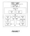
- FIG. 7is a block diagram of some electronic components, including a MIMO antenna, of a wireless communication terminal in accordance with some embodiments of the present invention.
- spatially relative termssuch as “above”, “below”, “upper”, “lower” and the like, may be used herein for ease of description to describe one element or feature's relationship to another element(s) or feature(s) as illustrated in the figures. It will be understood that the spatially relative terms are intended to encompass different orientations of the device in use or operation in addition to the orientation depicted in the figures. For example, if the device in the figures is turned over, elements described as “below” other elements or features would then be oriented “above” the other elements or features. Thus, the exemplary term “below” can encompass both an orientation of above and below. The device may be otherwise oriented (rotated 90 degrees or at other orientations) and the spatially relative descriptors used herein interpreted accordingly. Well-known functions or constructions may not be described in detail for brevity and/or clarity.
- Embodiments of the inventionare described herein with reference to schematic illustrations of idealized embodiments of the invention. As such, variations from the shapes and relative sizes of the illustrations as a result, for example, of manufacturing techniques and/or tolerances, are to be expected. Thus, embodiments of the invention should not be construed as limited to the particular shapes and relative sizes of regions illustrated herein but are to include deviations in shapes and/or relative sizes that result, for example, from different operational constraints and/or from manufacturing constraints. Thus, the elements illustrated in the figures are schematic in nature and their shapes are not intended to illustrate the actual shape of a region of a device and are not intended to limit the scope of the invention.
- wireless terminalthat includes a MIMO antenna that is configured to transmit and receive RF signals in two or more frequency bands.
- the MIMO antennamay be configured, for example, to transmit/receive RF communication signals in the frequency ranges used for cellular communications (e.g., cellular voice and/or data communications), WLAN communications, and/or TransferJet communications, etc.
- FIG. 1illustrates an exemplary MIMO antenna 100 that is configured in accordance with some embodiments.
- the MIMO antenna 100includes at least two radiating elements.
- a first radiating element 110 aincludes a straight portion 114 a connected to a serpentine-shaped portion 112 a .
- the straight and serpentine portions 114 a , 112 aare configured to resonate in at least two spaced apart RF frequency ranges in response to the straight portion being electrically excited through a first RF feed 116 a .
- a second radiating element 110 bincludes a straight portion 114 b connected to a serpentine-shaped portion 112 b .
- the straight and serpentine portions 114 b , 112 bare configured to resonate in at least two spaced apart RF frequency ranges in response to the straight portion being electrically excited through a second RF feed 116 b.
- the first and second radiating elements 110 a , 110 bmay be formed on a planar substrate, such as on a conventional printed circuit board, which includes a dielectric material, ceramic material, or insulation material.
- the first and second radiating elements 110 a , 110 bmay be adjacent to a ground plane 140 on the printed circuit board.
- the first and second radiating elements 110 a , 110 bmay be formed by patterning a conductive (e.g., metallization) layer on a printed circuit board.
- the MIMO antenna 100may further include first and second parasitic radiating elements 120 a , 120 b that are configured to resonate at a high frequency RF band that can be different than that of the serpentine portions.
- the first parasitic radiating element 120 ais adjacent and coupled to the first radiating element 110 a and, in particular, to the straight portion 114 a to radiate responsive to the straight portion 114 a of the first radiating element 110 a resonating at a RF frequency.
- the second parasitic radiating element 120 bis adjacent and coupled to the second radiating element 110 b and, in particular, to the straight portion 114 b to radiate responsive to the straight portion 114 b of the second radiating element 110 b resonating at a RF frequency.
- the first and second parasitic elements 120 a , 120 bmay provide a RF backscatter effect that may increase resonance within an operational RF frequency band and may, thereby, increase antenna efficiency and bandwidth of the first and second antenna elements 110 a , 110 b .
- the first and second parasitic elements 120 a , 120 bcan enable the antenna to have three or more RF bands of operation.
- the first and second radiating elements 110 a , 110 bmay be configured as a mirror image of each other, so that they have axial symmetry about a line equal distance between them. Accordingly, in some embodiments the straight portions 114 a , 114 b of the first and second radiating elements can have equal conductive path lengths, and the serpentine portions 112 a , 112 b can have equal conductive path lengths.
- the first and second radiating elements 110 a , 110 bcan be closely spaced.
- the spacing between the first and second radiating elements 110 a , 110 bmay be less than the combined lengths of each of their straight portions 114 a , 114 b and serpentine portions 112 a , 112 b , and may be spaced much closer together with the spacing therebetween being less than the conductive length of each of the straight portions 114 a , 114 b.
- first and second radiating elements 110 a , 110 bcan provide a more compact MIMO antenna structure and/or may simplify the transmitted and received circuitry that connects thereto.
- radiating elementsare necessarily spaced apart at much greater distances than what is shown in the exemplary embodiment of FIG. 1 in order to avoid undesirable cross coupling between the antenna elements, where RF signals transmitted by one antenna element induced undesirable interference currents in the adjacent antenna and vice versa.
- the first and second radiating elements 110 a , 110 bare at least partially decoupled by interconnecting the first and second radiating elements 110 a , 110 b through a conductive neutralization line 130 that conducts resonant currents therebetween to at least partially cancel RF transmission coupling between the first and second radiating elements 110 a , 110 b .
- a conductive path length of the conductive neutralization line 130can be configured to phase shift the conducted resonant currents to cause at least partial cancellation of RF signals wirelessly received by the first and second radiating elements from each other.
- the location which the conductive neutralization line 130 connects to the first and second radiating elements 110 a , 110 b and the conductive path length of the conductive neutralization line 130can be configured to phase shift the resonant current conducted from the first radiating element 110 a to the second radiating element 110 b to cause its subtraction from a current induced by a wireless RF signal received by the second radiating element 110 b from the first radiating element 110 a .
- the conductive neutralization line 130can be further configured to similarly phase shift the resonant current conducted from the second radiating element 110 b to the first radiating element 110 a to cause its subtraction from a current induced by a wireless RF signal received by the first radiating element 110 a from the second radiating element 110 b .
- cross-coupling of RF transmissions between the first and second radiating element 110 a , 110 bcan be at least partially cancelled through the feed-forward cross-coupling of phase-shifted resonant currents therebetween that at least partially cancels the RF signals that the first and second radiating element 110 a , 110 b receive from each other.
- the first and second radiating element 110 a , 110 bare configured to resonate in at least two RF frequency ranges.
- a low band resonant frequency and one of the high band resonant frequenciesare determined by the structure of their straight and serpentine portions.
- Another (third) resonant frequencyis determined by the configuration of their respective parasitic radiating element 120 a - b .
- the combined length of the straight and serpentine portions 114 a - b , 112 a - bmay be about a quarter wavelength of the low band resonant frequency.
- the length of the straight portions 114 a - bcan define one of the high band resonant frequencies due to a high impedance point being created close to a junction between the straight and serpentine portions.
- the high band RF signalis reflected by the high impedance point, resulting in the straight portions 114 a - b action as high band radiators.
- the higher frequency rangemay, in some embodiments, be at least twice as great as frequencies within the lower RF frequency range.
- the higher frequency rangemay include 5.2 GHz and the lower frequency range may include 2.4 GHz.
- the conductive length of the serpentine portion 112 a , 112 b of the first and second radiating elements 110 a , 110 bis at least four times greater than the conductive length of the respective straight portions 114 a , 114 b.
- the conductive neutralization line 130may include at least at least two abrupt opposite direction changes (e.g., a directional switchback) along its conductive path to decrease distance between the first and second radiating elements 110 a , 110 b.
- a directional switchbacke.g., a directional switchback
- the size of the MIMO antenna 100may be decreased by replacing a defined portion of the serpentine portions 112 a , 112 b with an inductive loaded antenna element.
- an RF signalcan enter RF feed 116 a and flow through the straight portion 114 a , a shortened serpentine portion 112 a , and then through an inductive load element.
- the second radiating element 110 bcan be similarly or identically configured with a shortened serpentine portion 112 b connected between the straight portion 114 b and an inductive load element.
- FIG. 2graph of antenna scattering parameters (S 11 , S 22 and S 21 ) versus frequency that may be generated by an operational simulation of the MIMO antenna of FIG. 1 .
- S 11 and S 22(collectively indicated by Curve 200 due to their symmetry causing overlapping curves) represent radiating elements 110 a and 110 b , respectively, and are measures of how much power (dB) is reflected back to transceiver circuitry connected thereto.
- S 21(indicated by Curve 210 ) represents the coupling that occurs between the antenna feed ports of the radiating elements 110 a , 110 b . Referring to FIG.
- FIG. 3is an exemplary graph of radiated power efficiency versus frequency that may be generated by an operational simulation of the MIMO antenna of FIG. 1 .
- the MIMO antenna 100has good power efficiency in each of the frequency bands 310 , 320 , 330 . Accordingly, although the first and second radiating elements 110 a , 110 b are spaced close together, they maintain high radiating power efficiency because of the decoupling therebetween that is created by operation of the conductive neutralization line 130 .
- FIG. 4is a plan view of a partial printed circuit board that includes a MIMO antenna 400 that is configured according to some other embodiments of the present invention.
- the MIMO antenna 400is similar to the MIMO antenna 100 of FIG. 1 , with the first and second radiating elements 410 a , 410 b each including a linear portion 114 a , 114 b connected to a respective serpentine-shape portion 112 a , 112 b .
- the linear portions 114 a , 114 breside on a substrate 420 surface that is angled relative to another surface on which the serpentine portions 112 a , 112 b reside.
- the linear portions 114 a , 114 blie in on a surface of the substrate 420 that is perpendicular to another surface of the substrate 420 on which the serpentine portions 112 a , 112 b lie.
- the substrate 420may be a conventional printed circuit board which includes a dielectric material, ceramic material, or insulation material.
- the MIMO antenna 400 shown in FIG. 4may provide a more compact structure that occupies less space and/or can reside in a smaller upper/lower/side portion of a communication device than the MIMO antenna 100 shown in FIG. 1 .
- FIG. 5is a plan view of a partial printed circuit board that includes a MIMO antenna 500 that is configured in accordance with some embodiments of the present invention to include two pairs of the dual antenna elements shown in FIG. 1 .
- the structure of the MIMO antenna 100 of FIG. 1has been duplicated and flipped to provide a MIMO antenna structure with four radiating elements.
- the MIMO antenna 500includes first and second radiating elements 110 a , 110 b , which may be identical to the same numbered features of FIG.
- third and fourth radiating elements 110 c , 110 dwhich may be configured as a mirror image of the respective first and second radiating elements 110 a , 110 b about an axis of symmetry that is about equal distance between those elements. Accordingly, the third and fourth radiating elements 110 c , 110 d can each include a straight portion that is connected between the RF feed and a serpentine-shape portion.
- a conductive neutralization line 510interconnects the conductive neutralization lines 130 between the first and second radiating elements 110 a , 110 b and between the third and fourth radiating elements 110 c , 110 d .
- a conductive path length of the conductive neutralization line 510can be configured to phase shift the conducted resonant currents to cause at least partial cancellation of RF signals wirelessly received by the third radiating element 110 c from the first radiating element 110 a , to cause at least partial cancellation of RF signals wirelessly received by the first radiating element 110 a from the third radiating element 110 c , to cause at least partial cancellation of RF signals wirelessly received by the fourth radiating element 110 d from the second radiating element 110 b , and to cause at least partial cancellation of RF signals wirelessly received by the second radiating element 110 b from the fourth radiating element 110 d .
- the conductive neutralization line 510may include abrupt directional changes, such as shown for the conductive neutralization line 130 in FIG. 1 , to decrease distance between
- FIG. 6is a plan view of a partial printed circuit board that includes a MIMO antenna 600 with two pairs of the dual antenna elements shown in FIG. 4 according to some embodiments of the present invention.
- the structure of the MIMO antenna 400 of FIG. 4has been duplicated and flipped to provide a MIMO antenna structure with four radiating elements.
- the MIMO antenna 600includes first and second radiating elements 410 a , 410 b , which may be identical to the same numbered features of FIG. 4 , and third and fourth radiating elements 410 c , 410 d which may be configured as a mirror image of the respective first and second radiating elements 410 a , 410 b about an axis of symmetry that is about equal distance between those elements.
- the third and fourth radiating elements 410 c , 410 dcan each include a straight portion that is connected between the RF feed and a serpentine-shape portion.
- the straight portions of the first, second, third, and fourth radiating elements 410 a , 410 b , 410 c , 410 dmay reside on a same planar substrate surface.
- the serpentine portions of the first and second radiating elements 410 a , 410 bmay reside on a substrate surface that is perpendicular (or angled at another angle) to the substrate surface on which the straight portions lie.
- the serpentine portions of the third and fourth radiating elements 410 c , 410 dmay reside on a substrate surface that is perpendicular (or angled at another angle) to the substrate surface on which the straight portions lie, and that substrate surface may be parallel to the substrate surface on which the serpentine portions of the first and second radiating elements 410 a , 410 b lie.
- a conductive neutralization line 620interconnects the conductive neutralization lines 130 between the first and second radiating elements 410 a , 410 b and between the third and fourth radiating elements 410 c , 410 d .
- a conductive path length of the conductive neutralization line 620can be configured to phase shift the conducted resonant currents to cause at least partial cancellation of RF signals wirelessly received by the third radiating element 410 c from the first radiating element 410 a , to cause at least partial cancellation of RF signals wirelessly received by the first radiating element 410 a from the third radiating element 410 c , to cause at least partial cancellation of RF signals wirelessly received by the fourth radiating element 410 d from the second radiating element 410 b , and to cause at least partial cancellation of RF signals wirelessly received by the second radiating element 410 b from the fourth radiating element 410 d .
- the conductive neutralization line 510may include abrupt directional changes, such as shown for the conductive neutralization
- FIG. 7is a block diagram of a wireless communication terminal 700 that includes a MIMO antenna in accordance with some embodiments of the present invention.
- the terminal 700includes a MIMO antenna 710 , a transceiver 740 , a processor 727 , and can further include a conventional display 708 , keypad 702 , speaker 704 , mass memory 728 , microphone 706 , and/or camera 724 , one or more of which may be electrically grounded to the same ground plane (e.g., ground plane 140 in FIG. 1 ) as the MIMO antenna 710 .
- the MIMO antenna 710may be structurally configured as shown for MIMO antenna 100 of FIG. 1 , MIMO antenna 400 of FIG. 4 , MIMO antenna 500 of FIG. 5 , MIMO antenna 600 FIG. 6 , or may be configured in accordance with various other embodiments of the present invention.
- the transceiver 740may include transmit/receive circuitry (TX/RX) that provides separate communication paths for supplying/receiving RF signals to different radiating elements of the MIMO antenna 710 via their respective RF feeds. Accordingly, when the MIMO antenna 710 includes two antenna elements, such as shown in FIG. 1 , the transceiver 740 may include two transmit/receive circuits 742 , 744 connected to different ones of the antenna elements via the respective RF feeds 116 a and 116 b.
- TX/RXtransmit/receive circuitry
- the transceiver 740 in operational cooperation with the processor 727may be configured to communicate according to at least one radio access technology in two or more frequency ranges.
- the at least one radio access technologymay include, but is not limited to, WLAN (e.g., 802.11), WiMAX (Worldwide Interoperability for Microwave Access), TransferJet, 3GPP LTE (3rd Generation Partnership Project Long Term Evolution), Universal Mobile Telecommunications System (UMTS), Global Standard for Mobile (GSM) communication, General Packet Radio Service (GPRS), enhanced data rates for GSM evolution (EDGE), DCS, PDC, PCS, code division multiple access (CDMA), wideband-CDMA, and/or CDMA2000.
- WLANe.g., 802.11
- WiMAXWorldwide Interoperability for Microwave Access
- TransferJetTransferJet
- 3GPP LTE3rd Generation Partnership Project Long Term Evolution
- UMTSUniversal Mobile Telecommunications System
- GSMGlobal Standard for Mobile
- GPRSGeneral Packet Radio Service
Landscapes
- Engineering & Computer Science (AREA)
- Computer Networks & Wireless Communication (AREA)
- Details Of Aerials (AREA)
- Variable-Direction Aerials And Aerial Arrays (AREA)
Abstract
Description
Claims (19)
Priority Applications (2)
| Application Number | Priority Date | Filing Date | Title |
|---|---|---|---|
| US12/837,018US8780002B2 (en) | 2010-07-15 | 2010-07-15 | Multiple-input multiple-output (MIMO) multi-band antennas with a conductive neutralization line for signal decoupling |
| EP11169721.5AEP2416444B1 (en) | 2010-07-15 | 2011-06-14 | Multiple-input multiple-output (MIMO) multi-band antennas with a conductive neutralization line for signal decoupling |
Applications Claiming Priority (1)
| Application Number | Priority Date | Filing Date | Title |
|---|---|---|---|
| US12/837,018US8780002B2 (en) | 2010-07-15 | 2010-07-15 | Multiple-input multiple-output (MIMO) multi-band antennas with a conductive neutralization line for signal decoupling |
Publications (2)
| Publication Number | Publication Date |
|---|---|
| US20120013519A1 US20120013519A1 (en) | 2012-01-19 |
| US8780002B2true US8780002B2 (en) | 2014-07-15 |
Family
ID=44675434
Family Applications (1)
| Application Number | Title | Priority Date | Filing Date |
|---|---|---|---|
| US12/837,018Active2031-08-01US8780002B2 (en) | 2010-07-15 | 2010-07-15 | Multiple-input multiple-output (MIMO) multi-band antennas with a conductive neutralization line for signal decoupling |
Country Status (2)
| Country | Link |
|---|---|
| US (1) | US8780002B2 (en) |
| EP (1) | EP2416444B1 (en) |
Cited By (2)
| Publication number | Priority date | Publication date | Assignee | Title |
|---|---|---|---|---|
| US10547099B2 (en) | 2015-11-02 | 2020-01-28 | Samsung Electronics Co., Ltd. | Antenna structure and electronic device including the same |
| US11088445B2 (en)* | 2018-04-20 | 2021-08-10 | Alpha Networks Inc. | Antenna assembly with compact layout traces |
Families Citing this family (83)
| Publication number | Priority date | Publication date | Assignee | Title |
|---|---|---|---|---|
| WO2011102143A1 (en)* | 2010-02-19 | 2011-08-25 | パナソニック株式会社 | Antenna device and portable wireless terminal equipped with same |
| CN102104193B (en)* | 2010-12-01 | 2015-04-01 | 中兴通讯股份有限公司 | Multiple input multiple output antenna system |
| KR101133343B1 (en)* | 2011-01-04 | 2012-04-06 | 인천대학교 산학협력단 | Mimo(multi input multi output) antenna without phase variation |
| FI20115072A0 (en)* | 2011-01-25 | 2011-01-25 | Pulse Finland Oy | Multi-resonance antenna, antenna module and radio unit |
| CN102959802B (en)* | 2011-04-11 | 2015-11-25 | 松下电器(美国)知识产权公司 | Antenna device and wireless communication device |
| US10129929B2 (en)* | 2011-07-24 | 2018-11-13 | Ethertronics, Inc. | Antennas configured for self-learning algorithms and related methods |
| US9354748B2 (en) | 2012-02-13 | 2016-05-31 | Microsoft Technology Licensing, Llc | Optical stylus interaction |
| USRE48963E1 (en) | 2012-03-02 | 2022-03-08 | Microsoft Technology Licensing, Llc | Connection device for computing devices |
| US8873227B2 (en) | 2012-03-02 | 2014-10-28 | Microsoft Corporation | Flexible hinge support layer |
| US9460029B2 (en) | 2012-03-02 | 2016-10-04 | Microsoft Technology Licensing, Llc | Pressure sensitive keys |
| US9075566B2 (en) | 2012-03-02 | 2015-07-07 | Microsoft Technoogy Licensing, LLC | Flexible hinge spine |
| US9360893B2 (en) | 2012-03-02 | 2016-06-07 | Microsoft Technology Licensing, Llc | Input device writing surface |
| US9298236B2 (en) | 2012-03-02 | 2016-03-29 | Microsoft Technology Licensing, Llc | Multi-stage power adapter configured to provide a first power level upon initial connection of the power adapter to the host device and a second power level thereafter upon notification from the host device to the power adapter |
| US9426905B2 (en) | 2012-03-02 | 2016-08-23 | Microsoft Technology Licensing, Llc | Connection device for computing devices |
| US9064654B2 (en) | 2012-03-02 | 2015-06-23 | Microsoft Technology Licensing, Llc | Method of manufacturing an input device |
| US9870066B2 (en) | 2012-03-02 | 2018-01-16 | Microsoft Technology Licensing, Llc | Method of manufacturing an input device |
| TWI511378B (en)* | 2012-04-03 | 2015-12-01 | Ind Tech Res Inst | Multi-band multi-antenna system and communiction device thereof |
| US20130300590A1 (en) | 2012-05-14 | 2013-11-14 | Paul Henry Dietz | Audio Feedback |
| US9073123B2 (en) | 2012-06-13 | 2015-07-07 | Microsoft Technology Licensing, Llc | Housing vents |
| US9684382B2 (en) | 2012-06-13 | 2017-06-20 | Microsoft Technology Licensing, Llc | Input device configuration having capacitive and pressure sensors |
| US9459160B2 (en) | 2012-06-13 | 2016-10-04 | Microsoft Technology Licensing, Llc | Input device sensor configuration |
| US8964379B2 (en) | 2012-08-20 | 2015-02-24 | Microsoft Corporation | Switchable magnetic lock |
| CN103682577B (en)* | 2012-08-31 | 2016-09-07 | 鸿富锦精密工业(深圳)有限公司 | Multifrequency antenna |
| CN102856646B (en)* | 2012-09-14 | 2014-12-10 | 重庆大学 | Decoupling matching network for compact antenna array |
| US8654030B1 (en) | 2012-10-16 | 2014-02-18 | Microsoft Corporation | Antenna placement |
| WO2014059618A1 (en) | 2012-10-17 | 2014-04-24 | Microsoft Corporation | Graphic formation via material ablation |
| EP2908970B1 (en) | 2012-10-17 | 2018-01-03 | Microsoft Technology Licensing, LLC | Metal alloy injection molding protrusions |
| WO2014059625A1 (en) | 2012-10-17 | 2014-04-24 | Microsoft Corporation | Metal alloy injection molding overflows |
| US10578499B2 (en) | 2013-02-17 | 2020-03-03 | Microsoft Technology Licensing, Llc | Piezo-actuated virtual buttons for touch surfaces |
| US9893427B2 (en) | 2013-03-14 | 2018-02-13 | Ethertronics, Inc. | Antenna-like matching component |
| CN103337697B (en)* | 2013-06-06 | 2015-04-15 | 电子科技大学 | Seven-band planar terminal antenna |
| DE102013107965B4 (en)* | 2013-07-25 | 2021-12-30 | Imst Gmbh | Antenna system with decoupling circuit |
| US9093750B2 (en)* | 2013-09-12 | 2015-07-28 | Laird Technologies, Inc. | Multiband MIMO vehicular antenna assemblies with DSRC capabilities |
| US9448631B2 (en) | 2013-12-31 | 2016-09-20 | Microsoft Technology Licensing, Llc | Input device haptics and pressure sensing |
| CN103794859B (en)* | 2014-01-18 | 2016-01-06 | 中国计量学院 | Three spring microstrip |
| US9759854B2 (en) | 2014-02-17 | 2017-09-12 | Microsoft Technology Licensing, Llc | Input device outer layer and backlighting |
| US10120420B2 (en) | 2014-03-21 | 2018-11-06 | Microsoft Technology Licensing, Llc | Lockable display and techniques enabling use of lockable displays |
| KR102375982B1 (en)* | 2014-03-31 | 2022-03-17 | 세키스이가가쿠 고교가부시키가이샤 | Interlayer film for laminated glass, and laminated glass |
| FR3021164B1 (en) | 2014-05-19 | 2018-05-11 | Centre National De La Recherche Scientifique | ANTENNA SYSTEM FOR REDUCING ELECTROMAGNETIC COUPLING BETWEEN ANTENNAS |
| CN104022353A (en)* | 2014-06-12 | 2014-09-03 | 电子科技大学 | Multi-band MIMO antenna used for intelligent machine |
| US10324733B2 (en) | 2014-07-30 | 2019-06-18 | Microsoft Technology Licensing, Llc | Shutdown notifications |
| US9424048B2 (en) | 2014-09-15 | 2016-08-23 | Microsoft Technology Licensing, Llc | Inductive peripheral retention device |
| US9728848B1 (en) | 2015-03-24 | 2017-08-08 | Amazon Technologies, Inc. | Adaptive neutralization line to counter environmental effects for ultra-high isolation |
| TWI560940B (en)* | 2015-03-31 | 2016-12-01 | Wistron Neweb Corp | Radio-frequency device and wireless communication device for enhancing antenna isolation |
| CN106159446B (en)* | 2015-04-07 | 2019-03-01 | 启碁科技股份有限公司 | Radio frequency device and wireless communication device |
| US9369187B1 (en)* | 2015-04-21 | 2016-06-14 | Amazon Technologies, Inc. | Antenna switching in an antenna system |
| US10222889B2 (en) | 2015-06-03 | 2019-03-05 | Microsoft Technology Licensing, Llc | Force inputs and cursor control |
| US10416799B2 (en) | 2015-06-03 | 2019-09-17 | Microsoft Technology Licensing, Llc | Force sensing and inadvertent input control of an input device |
| EP3381084B1 (en)* | 2015-11-25 | 2023-05-24 | CommScope Technologies LLC | Phased array antennas having decoupling units |
| US10061385B2 (en) | 2016-01-22 | 2018-08-28 | Microsoft Technology Licensing, Llc | Haptic feedback for a touch input device |
| KR102433402B1 (en)* | 2016-02-19 | 2022-08-17 | 삼성전자주식회사 | Antenna and electronic device comprising thereof |
| CN105846078A (en)* | 2016-05-23 | 2016-08-10 | 北京技德网络技术有限公司 | A new method for improving isolation between different antennas of radio equipment |
| JP6704169B2 (en)* | 2016-05-31 | 2020-06-03 | パナソニックIpマネジメント株式会社 | Dielectric substrate and antenna device |
| JP6730099B2 (en)* | 2016-06-07 | 2020-07-29 | 京セラ株式会社 | Antenna board and antenna device |
| US10615494B2 (en)* | 2016-09-08 | 2020-04-07 | Mediatek Inc. | Coupling reduction method for antennas in package |
| US10270162B2 (en) | 2016-09-23 | 2019-04-23 | Laird Technologies, Inc. | Omnidirectional antennas, antenna systems, and methods of making omnidirectional antennas |
| CN108232431A (en)* | 2016-12-22 | 2018-06-29 | 国基电子(上海)有限公司 | Antenna assembly |
| CN108281786A (en)* | 2017-01-05 | 2018-07-13 | 中兴通讯股份有限公司 | A kind of decoupling antenna frame and its decoupling method |
| US11043754B2 (en)* | 2017-01-25 | 2021-06-22 | Airties Kablosuz Iletisim Sanayi Ve Dis Ticaret A.S. | Method and apparatus for multi-feed multi-band MIMO antenna system |
| CN107275799B (en)* | 2017-04-28 | 2022-09-30 | 西安电子科技大学 | Parasitic antenna array for improving isolation of working frequency bands of multiple multi-frequency antennas |
| US10431877B2 (en) | 2017-05-12 | 2019-10-01 | Commscope Technologies Llc | Base station antennas having parasitic coupling units |
| CN108923813B (en)* | 2017-05-16 | 2020-11-27 | 联发科技股份有限公司 | RF equipment |
| US10535925B2 (en)* | 2017-09-08 | 2020-01-14 | Nxp B.V. | Wireless device antenna |
| TW201919283A (en) | 2017-11-09 | 2019-05-16 | 宏碁股份有限公司 | Mobile device |
| EP3794675B1 (en)* | 2018-06-29 | 2024-01-24 | Nokia Shanghai Bell Co., Ltd. | Multiband antenna structure |
| CN109149082B (en)* | 2018-07-18 | 2023-11-10 | 上海东洲罗顿通信股份有限公司 | Compact MIMO antenna and communication equipment comprising same |
| JP6678723B1 (en)* | 2018-10-31 | 2020-04-08 | 京セラ株式会社 | Antenna, wireless communication module and wireless communication device |
| CN109546337B (en)* | 2018-11-13 | 2020-11-10 | 北京理工大学 | Compact 5G mobile terminal MIMO antenna |
| WO2020190863A1 (en) | 2019-03-21 | 2020-09-24 | Commscope Technologies Llc | Base station antennas having parasitic assemblies for improving cross-polarization discrimination performance |
| CN112072303B (en)* | 2019-06-11 | 2021-07-06 | 苏州速感智能科技有限公司 | A kind of decoupling network, method and apparatus for installing decoupling network |
| CN110867641A (en)* | 2019-12-06 | 2020-03-06 | 惠州Tcl移动通信有限公司 | Mobile terminal MIMO antenna and mobile terminal equipment |
| CN113451771A (en)* | 2020-03-25 | 2021-09-28 | 中兴通讯股份有限公司 | Antenna device and communication terminal |
| CN113517557B (en) | 2020-04-10 | 2023-04-28 | 华为技术有限公司 | Electronic equipment |
| KR102501224B1 (en)* | 2021-06-30 | 2023-02-21 | 주식회사 에이스테크놀로지 | Omni-Directional MIMO Antenna |
| TWI738343B (en) | 2020-05-18 | 2021-09-01 | 為昇科科技股份有限公司 | Meander antenna structure |
| CN213636285U (en)* | 2020-09-24 | 2021-07-06 | 瑞声精密制造科技(常州)有限公司 | Antenna system and communication terminal |
| US11705618B2 (en)* | 2020-09-30 | 2023-07-18 | The Board Of Trustees Of The University Of Alabama | Ultrawide bandwidth, low-cost, roof-top mountable, low-profile, monocone antenna for vehicle-to-everything (V2X) communication |
| CN114512800B (en)* | 2020-11-17 | 2023-07-18 | 华为技术有限公司 | Antenna unit and electronic equipment including it |
| CN213520332U (en)* | 2020-12-04 | 2021-06-22 | 瑞声科技(新加坡)有限公司 | Antenna module and mobile terminal |
| TWI765743B (en)* | 2021-06-11 | 2022-05-21 | 啓碁科技股份有限公司 | Antenna structure |
| CN113540792B (en)* | 2021-07-21 | 2023-07-25 | 重庆传音通讯技术有限公司 | Antenna structure, terminal and terminal processing method |
| CN113764888B (en)* | 2021-08-09 | 2022-07-29 | 荣耀终端有限公司 | Antenna combination system and terminal equipment |
| CN115395231B (en)* | 2022-09-02 | 2023-04-18 | 安徽师范大学 | A Two-Port MIMO Antenna Based on Multiple Defective Grounds |
Citations (13)
| Publication number | Priority date | Publication date | Assignee | Title |
|---|---|---|---|---|
| WO2000001030A1 (en) | 1998-06-26 | 2000-01-06 | Racal Antennas Limited | Signal coupling methods and arrangements |
| WO2003077360A1 (en) | 2002-03-14 | 2003-09-18 | Sony Ericsson Mobile Communications Ab | Multiband planar built-in radio antenna with inverted-l main and parasitic radiators |
| US7355559B2 (en)* | 2004-08-21 | 2008-04-08 | Samsung Electronics Co., Ltd. | Small planar antenna with enhanced bandwidth and small strip radiator |
| US20080246689A1 (en) | 2007-04-06 | 2008-10-09 | Hong Fu Jin Precision Industry (Shenzhen) Co., Ltd. | Mimo antenna |
| US20090058735A1 (en)* | 2007-08-28 | 2009-03-05 | Hill Robert J | Hybrid slot antennas for handheld electronic devices |
| US20090174557A1 (en) | 2008-01-03 | 2009-07-09 | Intermec Ip Corp. | Compact flexible high gain antenna for handheld rfid reader |
| US20100001907A1 (en)* | 2008-07-01 | 2010-01-07 | Joymax Electronics Co., Ltd. | Compact planar antenna assembly |
| US7724201B2 (en)* | 2008-02-15 | 2010-05-25 | Sierra Wireless, Inc. | Compact diversity antenna system |
| US20100225553A1 (en)* | 2009-03-06 | 2010-09-09 | Thomson Licensing | Compact antenna system |
| EP2360787A2 (en) | 2009-11-30 | 2011-08-24 | Funai Electric Co., Ltd. | Multi-antenna apparatus |
| US20110221648A1 (en)* | 2009-01-02 | 2011-09-15 | Laird Technologies, Inc. | Multiband high gain omnidirectional antennas |
| US20110298666A1 (en)* | 2009-02-27 | 2011-12-08 | Mobitech Corp. | Mimo antenna having parasitic elements |
| US8130162B2 (en)* | 2003-08-07 | 2012-03-06 | Kildal Antenna Consulting Ab | Broadband multi-dipole antenna with frequency-independent radiation characteristics |
Family Cites Families (2)
| Publication number | Priority date | Publication date | Assignee | Title |
|---|---|---|---|---|
| US7688273B2 (en)* | 2007-04-20 | 2010-03-30 | Skycross, Inc. | Multimode antenna structure |
| KR100951582B1 (en)* | 2007-11-02 | 2010-04-09 | 한양대학교 산학협력단 | Ultra Wideband Diversity Antenna |
- 2010
- 2010-07-15USUS12/837,018patent/US8780002B2/enactiveActive
- 2011
- 2011-06-14EPEP11169721.5Apatent/EP2416444B1/ennot_activeNot-in-force
Patent Citations (14)
| Publication number | Priority date | Publication date | Assignee | Title |
|---|---|---|---|---|
| WO2000001030A1 (en) | 1998-06-26 | 2000-01-06 | Racal Antennas Limited | Signal coupling methods and arrangements |
| WO2003077360A1 (en) | 2002-03-14 | 2003-09-18 | Sony Ericsson Mobile Communications Ab | Multiband planar built-in radio antenna with inverted-l main and parasitic radiators |
| US8130162B2 (en)* | 2003-08-07 | 2012-03-06 | Kildal Antenna Consulting Ab | Broadband multi-dipole antenna with frequency-independent radiation characteristics |
| US7355559B2 (en)* | 2004-08-21 | 2008-04-08 | Samsung Electronics Co., Ltd. | Small planar antenna with enhanced bandwidth and small strip radiator |
| US7586445B2 (en)* | 2007-04-06 | 2009-09-08 | Hong Fu Jin Precision Industry (Shenzhen) Co., Ltd. | MIMO antenna |
| US20080246689A1 (en) | 2007-04-06 | 2008-10-09 | Hong Fu Jin Precision Industry (Shenzhen) Co., Ltd. | Mimo antenna |
| US20090058735A1 (en)* | 2007-08-28 | 2009-03-05 | Hill Robert J | Hybrid slot antennas for handheld electronic devices |
| US20090174557A1 (en) | 2008-01-03 | 2009-07-09 | Intermec Ip Corp. | Compact flexible high gain antenna for handheld rfid reader |
| US7724201B2 (en)* | 2008-02-15 | 2010-05-25 | Sierra Wireless, Inc. | Compact diversity antenna system |
| US20100001907A1 (en)* | 2008-07-01 | 2010-01-07 | Joymax Electronics Co., Ltd. | Compact planar antenna assembly |
| US20110221648A1 (en)* | 2009-01-02 | 2011-09-15 | Laird Technologies, Inc. | Multiband high gain omnidirectional antennas |
| US20110298666A1 (en)* | 2009-02-27 | 2011-12-08 | Mobitech Corp. | Mimo antenna having parasitic elements |
| US20100225553A1 (en)* | 2009-03-06 | 2010-09-09 | Thomson Licensing | Compact antenna system |
| EP2360787A2 (en) | 2009-11-30 | 2011-08-24 | Funai Electric Co., Ltd. | Multi-antenna apparatus |
Non-Patent Citations (4)
| Title |
|---|
| Diallo A. et al., "Enhanced two-antenna structures for universal mobile telecommunications system diversity terminals", IET Micorw. Antennas Propag., 2008, vol. 2, Issue 1, pp. 93-101. |
| European Office Action Corresponding to European Patent Application No. 11 169 721.5; Date Mailed: Nov. 27, 2013; 5 Pages. |
| European Search Report Corresponding to European Patent Application No. 11169721.5; Dated: Dec. 6, 2012; 17 Pages. |
| Park Y. et al., "Multi-band diversity antenna for mobile handset applications", Antennas and Propagation Society, International Symposium (APSURSI), IEEE, Jul. 11, 2010, 4 pages. |
Cited By (2)
| Publication number | Priority date | Publication date | Assignee | Title |
|---|---|---|---|---|
| US10547099B2 (en) | 2015-11-02 | 2020-01-28 | Samsung Electronics Co., Ltd. | Antenna structure and electronic device including the same |
| US11088445B2 (en)* | 2018-04-20 | 2021-08-10 | Alpha Networks Inc. | Antenna assembly with compact layout traces |
Also Published As
| Publication number | Publication date |
|---|---|
| US20120013519A1 (en) | 2012-01-19 |
| EP2416444A2 (en) | 2012-02-08 |
| EP2416444A3 (en) | 2013-01-09 |
| EP2416444B1 (en) | 2015-11-25 |
Similar Documents
| Publication | Publication Date | Title |
|---|---|---|
| US8780002B2 (en) | Multiple-input multiple-output (MIMO) multi-band antennas with a conductive neutralization line for signal decoupling | |
| US9397399B2 (en) | Loop antenna with switchable feeding and grounding points | |
| US8514134B2 (en) | MIMO antenna having parasitic elements | |
| US7408515B2 (en) | Mobile communication device and an antenna assembly for the device | |
| US6987483B2 (en) | Effectively balanced dipole microstrip antenna | |
| US8659482B2 (en) | MIMO antenna having plurality of isolation adjustment portions | |
| US9379433B2 (en) | Multiple-input multiple-output (MIMO) antennas with multi-band wave traps | |
| TWI506861B (en) | Switchable diversity antenna apparatus , mobile communications device , and low frequency range diversity antenna | |
| US9531084B2 (en) | Multiple input multiple output (MIMO) antennas having polarization and angle diversity and related wireless communications devices | |
| CN111180857A (en) | Antenna module and radio frequency device comprising same | |
| JP5631921B2 (en) | Multi-antenna and electronic device | |
| JP2006504308A (en) | Wireless device and antenna structure | |
| JP2012513730A (en) | Multi-port antenna structure and multi-mode antenna structure | |
| US9837726B2 (en) | Multi-band active integrated MIMO antennas | |
| US20110175783A1 (en) | Multilayer antenna | |
| WO2013175903A1 (en) | Antenna device and mimo wireless device | |
| US9385425B2 (en) | Antenna device | |
| US20150372383A1 (en) | Dual band antenna device | |
| US20090224984A1 (en) | Multi-Modal RF Diversity Antenna | |
| US10033097B2 (en) | Integrated antenna beam steering system | |
| JP4201274B2 (en) | Multi-band microstrip antenna and radio system using the same | |
| JP2006115451A (en) | Directional control microstrip antenna, radio module using the antenna, and radio system | |
| CN108428999B (en) | Antenna with a shield | |
| JP7040647B2 (en) | Antenna module and communication device equipped with it | |
| WO2024230933A1 (en) | Antenna apparatus and transceiver comprising the same |
Legal Events
| Date | Code | Title | Description |
|---|---|---|---|
| AS | Assignment | Owner name:SONY ERICSSON MOBILE COMMUNICATIONS AB, SWEDEN Free format text:ASSIGNMENT OF ASSIGNORS INTEREST;ASSIGNORS:HAKANSSON, MIKAEL;YING, ZHINONG;SIGNING DATES FROM 20100712 TO 20100715;REEL/FRAME:024691/0818 | |
| AS | Assignment | Owner name:SONY MOBILE COMMUNICATIONS AB, SWEDEN Free format text:CHANGE OF NAME;ASSIGNOR:SONY ERICSSON MOBILE COMMUNICATIONS AB;REEL/FRAME:033071/0806 Effective date:20120924 Owner name:SONY CORPORATION, JAPAN Free format text:ASSIGNMENT OF ASSIGNORS INTEREST;ASSIGNOR:SONY MOBILE COMMUNICATIONS AB;REEL/FRAME:032998/0199 Effective date:20140507 | |
| STCF | Information on status: patent grant | Free format text:PATENTED CASE | |
| AS | Assignment | Owner name:SONY MOBILE COMMUNICATIONS INC., JAPAN Free format text:ASSIGNMENT OF ASSIGNORS INTEREST;ASSIGNOR:SONY CORPORATION;REEL/FRAME:043943/0631 Effective date:20170914 | |
| AS | Assignment | Owner name:SONY MOBILE COMMUNICATIONS INC., JAPAN Free format text:ASSIGNMENT OF ASSIGNORS INTEREST;ASSIGNOR:SONY MOBILE COMMUNICATIONS AB;REEL/FRAME:043951/0529 Effective date:20170912 | |
| MAFP | Maintenance fee payment | Free format text:PAYMENT OF MAINTENANCE FEE, 4TH YEAR, LARGE ENTITY (ORIGINAL EVENT CODE: M1551) Year of fee payment:4 | |
| AS | Assignment | Owner name:SONY CORPORATION, JAPAN Free format text:ASSIGNMENT OF ASSIGNORS INTEREST;ASSIGNOR:SONY MOBILE COMMUNICATIONS, INC.;REEL/FRAME:048691/0134 Effective date:20190325 | |
| MAFP | Maintenance fee payment | Free format text:PAYMENT OF MAINTENANCE FEE, 8TH YEAR, LARGE ENTITY (ORIGINAL EVENT CODE: M1552); ENTITY STATUS OF PATENT OWNER: LARGE ENTITY Year of fee payment:8 |